KR20070085369A - Die-level traceability mechanism for semiconductor assembly and test facility - Google Patents
Die-level traceability mechanism for semiconductor assembly and test facility Download PDFInfo
- Publication number
- KR20070085369A KR20070085369A KR1020077011038A KR20077011038A KR20070085369A KR 20070085369 A KR20070085369 A KR 20070085369A KR 1020077011038 A KR1020077011038 A KR 1020077011038A KR 20077011038 A KR20077011038 A KR 20077011038A KR 20070085369 A KR20070085369 A KR 20070085369A
- Authority
- KR
- South Korea
- Prior art keywords
- die
- strings
- source object
- units
- string
- Prior art date
Links
- 230000007246 mechanism Effects 0.000 title claims abstract description 10
- 238000012360 testing method Methods 0.000 title description 10
- 239000004065 semiconductor Substances 0.000 title description 4
- 238000000034 method Methods 0.000 claims abstract description 45
- 238000004590 computer program Methods 0.000 claims abstract description 14
- 235000012431 wafers Nutrition 0.000 claims description 49
- 238000004519 manufacturing process Methods 0.000 claims description 21
- 239000000463 material Substances 0.000 abstract description 29
- 238000012546 transfer Methods 0.000 abstract description 24
- 238000012545 processing Methods 0.000 description 7
- 238000004806 packaging method and process Methods 0.000 description 3
- 239000000969 carrier Substances 0.000 description 2
- 240000005020 Acaciella glauca Species 0.000 description 1
- 101000730643 Homo sapiens Zinc finger protein PLAGL1 Proteins 0.000 description 1
- 235000011449 Rosa Nutrition 0.000 description 1
- 101100334474 Saccharomyces cerevisiae (strain ATCC 204508 / S288c) NOP1 gene Proteins 0.000 description 1
- 102100032570 Zinc finger protein PLAGL1 Human genes 0.000 description 1
- 230000009286 beneficial effect Effects 0.000 description 1
- 230000005540 biological transmission Effects 0.000 description 1
- 230000007547 defect Effects 0.000 description 1
- 238000005538 encapsulation Methods 0.000 description 1
- 238000005304 joining Methods 0.000 description 1
- 238000013508 migration Methods 0.000 description 1
- 230000005012 migration Effects 0.000 description 1
- 230000003287 optical effect Effects 0.000 description 1
- 238000003908 quality control method Methods 0.000 description 1
- 235000003499 redwood Nutrition 0.000 description 1
- 238000003860 storage Methods 0.000 description 1
Images


Classifications
-
- G—PHYSICS
- G06—COMPUTING; CALCULATING OR COUNTING
- G06Q—INFORMATION AND COMMUNICATION TECHNOLOGY [ICT] SPECIALLY ADAPTED FOR ADMINISTRATIVE, COMMERCIAL, FINANCIAL, MANAGERIAL OR SUPERVISORY PURPOSES; SYSTEMS OR METHODS SPECIALLY ADAPTED FOR ADMINISTRATIVE, COMMERCIAL, FINANCIAL, MANAGERIAL OR SUPERVISORY PURPOSES, NOT OTHERWISE PROVIDED FOR
- G06Q10/00—Administration; Management
- G06Q10/06—Resources, workflows, human or project management; Enterprise or organisation planning; Enterprise or organisation modelling
-
- H—ELECTRICITY
- H01—ELECTRIC ELEMENTS
- H01L—SEMICONDUCTOR DEVICES NOT COVERED BY CLASS H10
- H01L21/00—Processes or apparatus adapted for the manufacture or treatment of semiconductor or solid state devices or of parts thereof
- H01L21/02—Manufacture or treatment of semiconductor devices or of parts thereof
- H01L21/04—Manufacture or treatment of semiconductor devices or of parts thereof the devices having potential barriers, e.g. a PN junction, depletion layer or carrier concentration layer
- H01L21/18—Manufacture or treatment of semiconductor devices or of parts thereof the devices having potential barriers, e.g. a PN junction, depletion layer or carrier concentration layer the devices having semiconductor bodies comprising elements of Group IV of the Periodic Table or AIIIBV compounds with or without impurities, e.g. doping materials
- H01L21/30—Treatment of semiconductor bodies using processes or apparatus not provided for in groups H01L21/20 - H01L21/26
- H01L21/302—Treatment of semiconductor bodies using processes or apparatus not provided for in groups H01L21/20 - H01L21/26 to change their surface-physical characteristics or shape, e.g. etching, polishing, cutting
- H01L21/304—Mechanical treatment, e.g. grinding, polishing, cutting
-
- G—PHYSICS
- G06—COMPUTING; CALCULATING OR COUNTING
- G06Q—INFORMATION AND COMMUNICATION TECHNOLOGY [ICT] SPECIALLY ADAPTED FOR ADMINISTRATIVE, COMMERCIAL, FINANCIAL, MANAGERIAL OR SUPERVISORY PURPOSES; SYSTEMS OR METHODS SPECIALLY ADAPTED FOR ADMINISTRATIVE, COMMERCIAL, FINANCIAL, MANAGERIAL OR SUPERVISORY PURPOSES, NOT OTHERWISE PROVIDED FOR
- G06Q10/00—Administration; Management
- G06Q10/08—Logistics, e.g. warehousing, loading or distribution; Inventory or stock management
-
- H—ELECTRICITY
- H01—ELECTRIC ELEMENTS
- H01L—SEMICONDUCTOR DEVICES NOT COVERED BY CLASS H10
- H01L21/00—Processes or apparatus adapted for the manufacture or treatment of semiconductor or solid state devices or of parts thereof
Landscapes
- Engineering & Computer Science (AREA)
- Business, Economics & Management (AREA)
- Economics (AREA)
- Physics & Mathematics (AREA)
- General Physics & Mathematics (AREA)
- Strategic Management (AREA)
- Human Resources & Organizations (AREA)
- Entrepreneurship & Innovation (AREA)
- General Business, Economics & Management (AREA)
- Quality & Reliability (AREA)
- Theoretical Computer Science (AREA)
- Tourism & Hospitality (AREA)
- Development Economics (AREA)
- Marketing (AREA)
- Operations Research (AREA)
- Computer Hardware Design (AREA)
- Manufacturing & Machinery (AREA)
- Microelectronics & Electronic Packaging (AREA)
- Condensed Matter Physics & Semiconductors (AREA)
- Power Engineering (AREA)
- Educational Administration (AREA)
- Game Theory and Decision Science (AREA)
- General Factory Administration (AREA)
- Testing Or Measuring Of Semiconductors Or The Like (AREA)
Abstract
Description
본 출원은 35 U.S.C.§119에 따라 2005년 10월 15일자 출원되고 어플라이드 머티어리얼스 사에게 양도된 "반도체 조립 및 테스트 시설용 다이-레벨 추적 메커니즘"이란 제목의 미국 분할 출원 60/618,805호를 우선권으로 주장하며 상기 특허출원은 그 전체가 참조로 포함된다.This application supersedes US Application 60 / 618,805, entitled “Die-Level Tracking Mechanisms for Semiconductor Assembly and Test Facilities,” filed October 15, 2005 and assigned to Applied Materials in accordance with 35 USC§119. Which is incorporated by reference in its entirety.
본 발명의 실시예들은 대체로 예컨대 반도체 조립 및 테스트 시설의 팩토리 또는 로트로부터 다른 곳으로의 재료 이동 중에 다이 유닛을 추적하기 위한 시스템 및 방법에 관한 것이다.Embodiments of the present invention generally relate to systems and methods for tracking die units, for example, during material movement from a factory or lot in a semiconductor assembly and test facility.
반도체 칩 제조 공정에서, (다이 유닛으로 알려진) 다수의 다이들은 하나의 웨이퍼 상에서 제조된다. 그 후에 이들 다이는 분리되고 개별 칩으로 패키지화된다. 각각의 웨이퍼로부터의 칩의 수율은 제조 공정 동안의 결함으로 인해 100%가 되지 않는다. 하나의 웨이퍼로부터 얻어진 우수한 다이의 수는 수율을 결정한다. 다이 유닛은 통상적으로 여러 제조 및 품질 제어 동작을 위해 하나의 시설로부터 다른 시설로, 또는 로트에서 로트로 이송된다.In a semiconductor chip manufacturing process, multiple dies (known as die units) are manufactured on one wafer. These dies are then separated and packaged into individual chips. The yield of chips from each wafer is less than 100% due to defects during the manufacturing process. The number of good dies obtained from one wafer determines the yield. Die units are typically transferred from one facility to another, or from lot to lot for various manufacturing and quality control operations.
다이의 추적을 유지하기 위하여, 웨이퍼 상의 각각의 다이 유닛은 고유 식별 자(다이 ID)가 부여되고, 각각의 웨이퍼는 로트와 같이 웨이퍼 그룹으로 할당된다. 로트 내의 웨이퍼는 종종 로트의 재료로서 추적된다. 제조 실행 시스템(MES)에서 로트와 재료 오브젝트는 팩토리의 물리적 아이템의 대표이다. 다이 ID는 임의의 형태로 이루어질 수 있으며 한가지 규정(convention)은 다이 ID가 (반드시 그러하진 않지만) ID가 위치한 로트와 관련한 정보를 포함하는 식별자(또는 다이의 식별자의 일부)로서 웨이퍼 상에서 다이의 좌표 위치를 사용하는 것이다. 다이에 대응하는 추가 정보는 추가 스트링 내에 부여되고, 이러한 추가 스트링은 결합된 다이 ID와 함께 로트 또는 기타 재료의 다이 정보를 구성한다. 예컨대, 사용자는 제품, 등급 등과 같은 정보를 로트의 각각의 다이에 추가하기를 원할 수 있다. 이러한 정보는 추가 스트링 내에서 수행될 수 있다. 다이 ID의 해당 요소가 추가 스트링과 매칭할 때, 개별 다이의 정보, 즉 다이 ID, 및 그 제품이 얻어질 수 있다. To keep track of the die, each die unit on the wafer is assigned a unique identifier (die ID), and each wafer is assigned to a group of wafers, such as a lot. Wafers in a lot are often tracked as the material of the lot. In the Manufacturing Execution System (MES), the lot and material objects are representative of the physical items of the factory. The die ID can be in any form and one convention is that the die ID (or not necessarily) is an identifier (or part of the die's identifier) that contains information relating to the lot in which the ID is located and the coordinates of the die on the wafer. Is to use location. Additional information corresponding to the die is given in an additional string, which, together with the combined die ID, constitutes the die information of the lot or other material. For example, a user may want to add information such as product, grade, etc. to each die of the lot. This information can be performed in an additional string. When the corresponding element of the die ID matches the additional string, the information of the individual die, namely the die ID, and its product can be obtained.
하나의 로트로부터 또 다른 로트로 적어도 일부 다이 유닛의 이송이 존재할 때, 웨이퍼 및 로트 정보에 따른 해당 다이 정보는 새로운 로트로 통과될 필요가 있다. 이러한 다이 정보는 다이 유닛 레벨에서 수행될 동작 관점에서 개별 다이의 히스토리, 운송에 사용된 캐리어, 여러 횟수에 속하는 로트, 및 다른 히스토리 정보를 추적하는데 유용하다.When there is a transfer of at least some die units from one lot to another, the corresponding die information according to the wafer and lot information needs to be passed through to a new lot. This die information is useful for tracking the history of individual dies, carriers used for transportation, lots belonging to a number of times, and other history information in terms of operations to be performed at the die unit level.
종래 조립 동작에서, 다이 유닛은 예컨대 제 1 로트 내의 제 1 웨이퍼로부터의 공정을 위해 끌어당겨질 수 있다. 선택적으로, 다이 유닛은 다수의 위치로부터 끌어 당겨질 수 있다. 단일 웨이퍼의 여러 위치로부터, 여러 웨이퍼로부터, 및 여러 웨이퍼 로트로부터 상호-혼합된(co-mingle) 우수한 다이는 통상적으로 조립 동 작 동안 발생할 수 있다. 불행히도, 다수의 웨이퍼와 다수의 로트 중의 다이 유닛은 상호-혼합되고, 특정 다이 유닛에 대한 추적성은 잃게 된다. 만약 그 후에 다이가 필드 내에서 신뢰할 수 없는 것으로 밝혀지면, 다이 유닛의 소스를 밝히는 것이 제조자의 관점에서 유익하다. 또한 어떻게 언제 다이 유닛이 제조되었는지를 결정하는 것이 바람직하다. 이러한 표시는 다이 유닛이 운송된 이후에 뿐만 아니라 운송 이전에 다이 유닛의 테스트 동안 제조 공정을 개선하는데 제조자에게 도움을 준다. In a conventional assembly operation, the die unit may be pulled for processing from the first wafer, for example in the first lot. Optionally, the die unit can be pulled from multiple locations. Excellent die co-mingle from multiple locations, from multiple wafers, and from multiple wafer lots of a single wafer can typically occur during assembly operations. Unfortunately, die units in multiple wafers and multiple lots are inter-mixed, and traceability to a particular die unit is lost. If the die is subsequently found to be unreliable in the field, identifying the source of the die unit is beneficial from the manufacturer's point of view. It is also desirable to determine how and when the die unit was manufactured. This marking aids the manufacturer in improving the manufacturing process during the testing of the die unit as well as after the die unit has been shipped.
다이 유닛을 추적하는데 사용된 종래 기술은 주로 다이 유닛이 하나의 로트로부터 다른 로트로 이송될 때 다이 ID를 수동조작하는 것으로 제한된다. 이러한 작업의 복잡성과 종종 포함된 많은 양의 정보로 인해, 이러한 수동조작은 느리고 번거로운 공정이 될 수 있다. 따라서 수용 오브젝트 내의 이송된 다이 유닛의 다이 ID를 조절하고, 소스 오브젝트 내에 남아있는 다이 유닛의 다이 ID를 조절하는 번거로운 공정을 피하는 것이 바람직하다. 따라서, 본 발명은 이러한 문제점 뿐만 아니라 기타 중용한 목적에 관한 것이다.The prior art used to track die units is mainly limited to manually manipulating the die ID when the die unit is transferred from one lot to another. Due to the complexity of this task and the large amount of information often included, this manual operation can be a slow and cumbersome process. Therefore, it is desirable to avoid the cumbersome process of adjusting the die ID of the transferred die unit in the receiving object and adjusting the die ID of the die unit remaining in the source object. Accordingly, the present invention relates to these problems as well as other important objects.
본 발명은 예컨대 하나의 팩토리 또는 로트로부터 다른 곳으로의 재료 이송 동안 다이 유닛을 추적하기 위한 새로운 방법, 시스템 및 컴퓨터 프로그램 제품을 제공하며 예컨대 로트 이송 공정 동안 다이 데이터와 개별 다이 간의 대응성을 유효하게 유지한다. 본 발명의 하나 이상의 실시예들은 개별 다이 ID를 각각의 다이 유닛, 예컨대 각각의 로트에 할당하고, 대응하는 다이 ID의 범위를 인덱스 스트링으로 연관시킴으로써 다이-레벨 추적성의 메커니즘을 개선하고자 하는 것이다. 다이 ID는 웨이퍼 ID, X-좌표, 및 Y-좌표를 포함할 수 있으며, 기타 다이-관련 정보를 포함할 수 있다. 로트 또는 재료 오브젝트의 다이 정보는 다이 ID 및 추가 스트링을 포함한다. 예컨대 일부 다이가 예컨대 제 1 로트로부터 제 2 로트로 이송될 때, 제 1 로트와 관련한 전체 다이 정보는 제 2 로트에 복사되고, 상이한 인덱스 스트링은 제 2 로트에 할당되어 이송된 실제 다이 또는 다이 범위를 나타낸다. 다음에 제 1 로트의 인덱스 스트링은 이송 후에 제 1 로트에 남아 이는 다이를 나타내도록 조절된다. 인덱스 스트링을 사용함으로써, 특정 로트의 다이는 예컨대 제 1 로트로부터 제 2 로트로 선택된 다이를 이송하는 과정 중에 상이한 로트(및 그 안의 다이)를 개별 다이 ID와 선택적으로 연관시키고 및/또는 수동조작할 필요없이 추적을 보다 유효하게 유지할 수 있다.The present invention provides, for example, new methods, systems and computer program products for tracking die units during material transfer from one factory or lot to another, for example to effectively support the correspondence between die data and individual die during a lot transfer process. Keep it. One or more embodiments of the present invention seek to improve the mechanism of die-level traceability by assigning individual die IDs to each die unit, such as each lot, and associating a range of corresponding die IDs with an index string. Die IDs may include wafer IDs, X-coordinates, and Y-coordinates, and may include other die-related information. The die information of the lot or material object includes the die ID and the additional string. For example, when some die is transferred from, for example, the first lot to the second lot, the entire die information associated with the first lot is copied to the second lot, and different index strings are assigned to the second lot and the actual die or die range transferred. Indicates. The index string of the first lot then remains in the first lot after the transfer and is adjusted to represent the die. By using an index string, a die of a particular lot may optionally associate and / or manually manipulate a different lot (and die therein) with an individual die ID during the process of transferring the selected die from the first lot to the second lot, for example. You can keep the trace more effective without the need.
따라서, 본 발명은 제 1 인덱스 스트링을 다수의 다이 유닛에 대한 일대일 대응하는 다수의 다이 스트링에 할당하는 - 상기 다수의 다이 유닛은 소스 오브젝트와 연관되고, 제 1 인덱스 스트링 식별자에 의해 포함된 각각의 인덱스의 범위는 상기 다수의 다이 스트링 중 하나를 식별함 - 소스 오브젝트로부터 수용 오브젝트로 다이 유닛의 적어도 일부를 이송할 때 다수의 다이 유닛과 연관된 다수의 다이 스트링을 소스 오브젝트로부터 수용 오브젝트로 복사하고, 수용 오브젝트로 이송된 다이 유닛을 나타내도록 소스 오브젝트로부터 수용 오브젝트로 이송된 다이 유닛과 연관된 다이 스트링에 제 2 인덱스 스트링을 할당하고, 소스 오브젝트에 남아있는 다이 유닛을 나타내도록 소스 오브젝트의 제 1 인덱스 스트링을 조절하는 동작 단계들을 포함하는 제조 동작 중에 다이 유닛을 추적하는 방법에 관한 것이다. 특히, 다이 스트링은 웨이퍼 ID와 다이 좌표를 포함하고, 각각의 다이 좌표는 X-좌표 및 Y-좌표를 포함하며, 다이 스트링은 웨이퍼 ID와 숫자 시퀀스의 범위를 포함하며, 상기 방법의 다이 스트링은 소스 오브젝트의 다이 맵으로부터 생성된다. 일 예에서, 소스 오브젝트는 다수의 웨이퍼이고 수용 오브젝트는 다수의 리드 프레임이다. 또 다른 예에서, 소스 오브젝트는 제 1 다수의 리드 프레임이고 수용 오브젝트는 제 2 다수의 매거진이다.Accordingly, the present invention assigns a first index string to a one-to-one corresponding multiple die string for multiple die units, wherein the multiple die units are associated with the source object and each of which is contained by the first index string identifier. A range of indices identifies one of the plurality of die strings—copying the plurality of die strings associated with the plurality of die units from the source object to the receiving object when transferring at least a portion of the die unit from the source object to the receiving object, Allocate a second index string to a die string associated with the die unit transferred from the source object to the receiving object to represent the die unit transferred to the receiving object, and the first index string of the source object to indicate the die unit remaining in the source object. And comprising operating steps to adjust A method of tracking a die unit during jaw operation. In particular, the die string includes a wafer ID and die coordinates, each die coordinate includes an X-coordinate and a Y-coordinate, the die string includes a wafer ID and a range of numeric sequences, and the die string of the method Generated from the die map of the source object. In one example, the source object is a plurality of wafers and the receiving object is a plurality of lead frames. In another example, the source object is a first plurality of lead frames and the receiving object is a second plurality of magazines.
본 발명의 일 예에서, 제조 동작 동안 다이 유닛을 추적하는 방법은 상기 다수의 다이 스트링에 일대일 대응하게 다수의 사용자-정의 스트링을 할당하는 동작 단계들을 더 포함한다. In one example of the present invention, a method of tracking a die unit during a manufacturing operation further comprises the steps of assigning a plurality of user-defined strings one-to-one corresponding to the plurality of die strings.
본 발명의 또 다른 예에서, 제조 동작 동안 다이 유닛을 추적하기 위한 방법은 상기 다수의 다이 스트링에 일대일 대응하게 다이 픽킹 순서를 할당하는 동작 단계들을 더 포함한다. In another example of the invention, a method for tracking a die unit during a manufacturing operation further includes the steps of assigning a die picking order one-to-one corresponding to the plurality of die strings.
본 발명의 또 다른 예에서, 제조 동작 동안 다이 유닛을 추적하는 방법은 소스 오브젝트로부터 수용 오브젝트로 이송된 다이 유닛과 연관된 상기 인덱스 스트링과 다이 스트링을 저장하는 동작 단계들을 더 포함하며, 저장된 인덱스 스트링과 다이 스트링은 다이 유닛의 히스토리를 추적하고 다이 유닛 추적 정보를 포함하는 보고서를 생성한다.In another example of the invention, a method of tracking a die unit during a manufacturing operation further comprises operating steps for storing the index string and die string associated with the die unit transferred from a source object to a receiving object, The die string tracks the history of the die unit and generates a report containing the die unit tracking information.
하나 이상의 실시예에서, 본 발명은 제조 동작 동안 다이 유닛을 추적하기 위한 시스템에 관한 것이며, 상기 시스템은 다수의 다이 유닛에 일대일 대응하게 제 1 인덱스 스트링을 고유 할당된 다수의 다이 스트링으로 할당하는 프로세서 - 상기 다수의 다이 유닛은 소스 오브젝트와 연관되고, 제 1 인덱스 스트링의 각각의 인덱스는 상기 다수의 다이 스트링 중 하나를 식별함 - 및 소스 오브젝트로부터 수용 오브젝트로 이송된 적어도 일부 다이 유닛을 추적하는 추적 메커니즘을 포함하며, 상기 추적 메커니즘은 소스 오브젝트로부터 수용 오브젝트로 이송된 다이 유닛과 연관된 적어도 일부 다이 스트링을 복사하고, 제 2 인덱스 스트링을 소스 오브젝트로부터 수용 오브젝트로 이송된 다이 유닛과 연관된 다이 스트링으로 할당하고 소스 오브젝트에 남아있는 다이 유닛을 나타내도록 소스 오브젝트 내의 제 1 인덱스 스트링을 조절한다.In one or more embodiments, the present invention is directed to a system for tracking die units during a manufacturing operation, the system comprising: a processor that assigns a first index string to a uniquely assigned plurality of die strings in a one-to-one correspondence to the plurality of die units; The plurality of die units are associated with a source object, each index of the first index string identifies one of the plurality of die strings, and tracking at least some die units transferred from the source object to the receiving object. A mechanism, wherein the tracking mechanism copies at least some die strings associated with the die units transferred from the source object to the receiving object and assigns a second index string to the die strings associated with the die units transferred from the source object to the receiving object. And remain in the source object Adjust the first index string in the source object to indicate the die unit in which it is located.
일 예에서, 본 발명에 따른 시스템은 소스 오브젝트의 다이 맵으로부터 다이 스트링을 생성하기 위한 다이 접합 장치를 더 포함한다. In one example, the system according to the invention further comprises a die bonding apparatus for generating a die string from a die map of the source object.
또 다른 예에서, 본 발명에 따른 시스템은 소스 오브젝트로부터 수용 오브젝트로 이송된 다이 유닛과 관련된 인덱스 스트링 및 다이 스트링을 저장하기 위한 다이 히스토리 표을 더 포함한다. In another example, the system according to the invention further comprises a die history table for storing the die string and the index string associated with the die unit transferred from the source object to the receiving object.
또 다른 예에서, 본 발명은 제조 동작 동안 다이 유닛을 추적하기 위한 시스템에 관한 것이며 상기 시스템은 다수의 다이 유닛에 일대일 대응하게 제 1 인덱스 스트링을 고유 할당된 다수의 다이 스트링에 할당하기 위한 수단 - 상기 다수의 다이 유닛은 소스 오브젝트와 연관되고, 제 1 인덱스 스트링에 의해 포함된 각각의 범위의 인덱스는 상기 다수의 다이 스트링 중 하나를 식별함 - , 적어도 일부 다이 유닛을 소스 오브젝트로부터 수용 오브젝트로 이송할 때 소스 오브젝트로부터 수용 오브젝트로 다수의 다이 유닛과 연관된 다수의 다이 스트링을 복사하기 위한 수단, 수용 오브젝트로 이송된 다이 유닛을 나타내기 위해 소스 오브젝트로부터 수용 오브젝트로 이송된 다이유닛과 연관된 다이 스트링으로 제 2 인덱스 스트링을 할당하기 위한 수단, 및 소스 오브젝트에 남아있는 다이 유닛을 나타내도록 소스 오브젝트의 제 1 인덱스 스트링을 조절하기 위한 수단을 포함한다. 특히, 다이 스트링은 웨이퍼 ID 및 다이 좌표를 포함하고, 다이 스트링은 소스 오브젝트의 다이 맵으로부터 생성되고, 다이 좌표는 X-좌표 및 Y-좌표를 포함한다. 일 예에서, 다이 스트링은 웨이퍼 ID 및 숫자 시퀀스 범위를 포함한다. 본 발명에 따른 시스템의 일 예에서, 소스 오브젝트는 다수의 웨이퍼이고 수용 오브젝트는 다수의 리드 프레임이다. 또 다른 예에서, 소스 오브젝트는 다수의 리드 프레임이고 수용 오브젝트는 다수의 매거진이다.In another example, the invention relates to a system for tracking die units during a manufacturing operation, the system comprising means for assigning a first index string to a uniquely assigned plurality of die strings in a one-to-one correspondence to the plurality of die units; The plurality of die units are associated with a source object, and the index of each range included by the first index string identifies one of the plurality of die strings, transferring at least some die units from the source object to the receiving object. Means for copying a plurality of die strings associated with a plurality of die units from a source object to a receiving object, to a die string associated with a die unit transferred from a source object to a receiving object to represent a die unit transferred to a receiving object. Means for assigning a second index string, and Means for adjusting the first index string of the source object to indicate a die unit remaining in the source object. In particular, the die string includes a wafer ID and die coordinates, the die string is generated from a die map of the source object, and the die coordinates include X- and Y-coordinates. In one example, the die string includes a wafer ID and a numeric sequence range. In one example of a system according to the invention, the source object is a plurality of wafers and the receiving object is a plurality of lead frames. In another example, the source object is a number of lead frames and the receiving object is a number of magazines.
일 예에서, 본 발명에 따른 시스템은 상기 다수의 다이 스트링에 일대일 대응하게 다수의 사용자-정의 스트링을 할당하기 위한 수단을 더 포함한다.In one example, the system according to the invention further comprises means for assigning a plurality of user-defined strings in a one-to-one correspondence to the plurality of die strings.
또 다른 예에서, 본 발명에 따른 시스템은 상기 다수의 다이 스트링에 일대일 대응하게 다이 픽킹 순서를 할당하기 위한 수단을 더 포함한다.In another example, the system according to the invention further comprises means for assigning a die picking order in a one-to-one correspondence to the plurality of die strings.
또 다른 예에서, 본 발명에 따른 시스템은 소스 오브젝트로부터 수용 오브젝트로 이송된 다이 유닛과 연관된 인덱스 스트링 및 다이 스트링을 저장하기 위한 수단을 더 포함한다.In another example, the system according to the invention further comprises means for storing the die string and the index string associated with the die unit transferred from the source object to the receiving object.
또한 본 발명의 일 예는 컴퓨터 판독가능 매체에 저장된 컴퓨터 프로그램 제품에 관한 것이며, 상기 컴퓨터 프로그램 제품은 컴퓨터가 제 1 인덱스 스트링을 다수의 다이 유닛에 일대일 대응하게 고유 할당된 다수의 다이 스트링에 할당시키고 - 상기 다수의 다이 유닛은 소스 오브젝트와 연관되고, 제 1 인덱스 스트링에 의해 포함된 각각의 범위의 인덱스는 다수의 스트링 중 하나를 식별함 - , 소스 오브젝트로부터 수용 오브젝트로 적어도 일부의 다이 유닛을 이송할 때 소스 오브젝트로부터 수용 오브젝트로 다수의 다이 유닛과 연관된 다수의 다이 스트링을 복사하고, 수용 오브젝트에 이송된 다이 유닛을 나타내도록 제 2 인덱스 스트링을 소스 오브젝트로부터 수용 오브젝트로 이송된 다이 유닛과 연관된 다이 스트링으로 할당하고, 소스 오브젝트에 남아있는 다이 유닛을 나타내도록 소스 오브젝트의 제 1 인덱스 스트링을 조절하게 하는 명령어들을 포함한다.An example of the invention also relates to a computer program product stored on a computer readable medium, wherein the computer program product allows a computer to assign a first index string to a plurality of die strings that are uniquely assigned to the plurality of die units one-to-one correspondingly. The plurality of die units are associated with a source object, and the index of each range included by the first index string identifies one of the plurality of strings, transferring at least some die units from the source object to the receiving object. Copy the plurality of die strings associated with the plurality of die units from the source object to the receiving object and the second index string associated with the die unit transferred from the source object to the receiving object to indicate the die unit transferred to the receiving object. Assign it as a string, Instructions for adjusting the first index string of the source object to indicate the remaining die unit.
일 예에서, 본 발명에 따른 컴퓨터 프로그램 제품은 컴퓨터가 상기 다수의 다이 스트링에 일대일 대응하게 다수의 사용자-정의 스트링을 할당하게 하는 명령어들을 더 포함한다.In one example, a computer program product according to the present invention further includes instructions for causing a computer to assign a plurality of user-defined strings in a one-to-one correspondence to the plurality of die strings.
또 다른 예에서, 본 발명에 따른 컴퓨터 프로그램 제품은 컴퓨터가 다수의 다이 스트링에 일대일로 대응하게 다이 픽킹 순서를 할당하게 하는 명령어들을 더 포함한다.In another example, a computer program product according to the present invention further includes instructions for causing a computer to assign die picking order in a one-to-one correspondence to a plurality of die strings.
또 다른 예에서, 본 발명에 따른 컴퓨터 프로그램 제품은 컴퓨터가 소스 오브젝트로부터 수용 오브젝트로 이송된 다이 유닛과 연관된 인덱스 스트링 및 다이 스트링을 저장하게 하는 명령어들을 더 포함한다. In another example, the computer program product according to the present invention further includes instructions for causing the computer to store the index string and the die string associated with the die unit transferred from the source object to the receiving object.
도 1은 본 발명에 따른 예시적인 다이-레벨 추적 시스템의 일 예이다.1 is an example of an exemplary die-level tracking system in accordance with the present invention.
도 2는 본 발명에 따른 다이-추적 메커니즘의 예시적인 실시예에 따른 흐름도이다.2 is a flow chart according to an exemplary embodiment of a die-tracking mechanism according to the present invention.
도 3은 웨이퍼를 위한 예시적인 다이 픽킹 패턴을 도시한다.3 shows an exemplary die picking pattern for a wafer.
도 4는 웨이퍼의 다이 픽킹 순서에 대한 일 예를 도시한다.4 shows an example of the die picking order of a wafer.
도 5는 스플릿 로트 처리(transaction)시 하나의 로트로부터 또 다른 로트로의 다이 유닛의 이송 전후에 로트 내의 예시적인 다이 데이터를 도시한다.5 shows exemplary die data in a lot before and after transfer of a die unit from one lot to another during a split lot transaction.
도 6은 합병 로트 처리시 하나의 로트로부터 또 다른 로트로의 다이 유닛의 이송 전후에 로트 내의 예시적인 다이 데이터를 도시한다.6 shows exemplary die data in a lot before and after transfer of a die unit from one lot to another during a merged lot process.
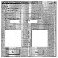
도 7은 로트 또는 재료 동작을 위해 다이 ID를 특정하는데 사용된 본 발명을 위한 예시적인 그래픽 사용자 인터페이스(UI)를 도시한다.7 illustrates an exemplary graphical user interface (UI) for the present invention used to specify a die ID for lot or material operation.
도 8은 로트 또는 재료 동작을 위해 다이 ID를 특정하는데 사용된 본 발명을 위한 예시적인 또 다른 그래픽 사용자 인터페이스(UI)를 도시한다.8 illustrates another exemplary graphical user interface (UI) for the present invention used to specify a die ID for lot or material operation.
도 9는 다이 추적 정보를 검색하는데 사용된 본 발명을 위한 예시적인 그래픽 사용자 인터페이스를 도시한다.9 illustrates an exemplary graphical user interface for the present invention used to retrieve die tracking information.
본 발명의 실시예들은 예컨대 하나의 로트의 일부가 또 다른 로트로 이송되는 제조 동작 중의 다이 유닛 추적을 용이하게 하는 다이-레벨 추적 시스템, 방법 및 제품을 제공한다. 이제 도면을 참조하자면, 특히 도 1을 참조하면, 예컨대 하나의 팩토리 또는 로트로부터 또 다른 곳으로의 재료 이송 동안 다이 유닛의 추적을 용이하게 하고 예컨대 로트 이송 공정 중에 다이 데이터와 개별 다이 간의 대응 성을 유효하게 유지시키기 위한, 100으로 표시된 다이-레벨 추적 시스템이 도시되어 있다. 시스템(100)은 하나 이상의 제조 시스템(102), 테스팅, 조립 및 패키징 시스템(104)(예컨대 FLEXTM 테스트 시스템, Teradyne, Inc., Boston,,MA), 호스트 네트워크(106), 사용자 인터페이스(108), 어플리케이션 서버(110)(예컨대 IBM WebSphere® Application Server, IBM Corporation, Armonk, NY), 및 데이터 베이스(112)(예컨대, Oracle, Oracle Corporation, Redwood Shores, CA)를 포함할 수 있다. 테스팅, 조립 및 패키징 시스템(104)은 예컨대 웨이퍼 테스팅(104a)(예컨대 APT System, Keithley Instruments, Inc., Cleveland, OH), 다이싱(104b)(예컨대, Dynatex Wafer Dicing System, Dynatex International, Santa Rosa, CA), 하나의 와이어 접합(104c)(예컨대 Kulicke & Soffa, Willow Grove, PA), 캡슐화(104d), 및 테스트와 번-인(104e)와 관련된 동작들을 수행하기 위한 장치들을 포함할 수 있다. 임의 수의 상이한 장치와 공정은 당업자에게 용이하게 알려진 것처럼 시스템(100)과 함께 사용되도록 고려된다.Embodiments of the present invention provide die-level tracking systems, methods, and products that facilitate die unit tracking during manufacturing operations, for example, where a portion of one lot is transferred to another lot. Referring now to the drawings, and in particular with reference to FIG. 1, for example, it facilitates the tracking of the die unit during material transfer from one factory or lot to another and facilitates the correspondence between die data and individual die during, for example, a lot transfer process. A die-level tracking system, shown at 100, is shown to remain valid.
본 발명의 하나 이상의 실시예에서, 어플리케이션 서버(110)는 사용자로부터 각각의 다이 유닛에 대한 다이 ID를 생성한다. 어플리케이션 서버(110)는 다이 ID를 다이 유닛에 일대일 대응하게 할당한다. 본 발명의 또 다른 실시예에서 다이 ID는 제조 시스템(102)에 의해 생성된다. 다이 ID는 어플리케이션 또는 툴(tool)에 의해 외부적으로 생성되거나 사용자-정의된 자유로운 형태의 스트링(다이 스트링)일 수 있다. 생성된 다이 ID는 데이터베이스(112) 내에 저장된다. 로트 또는 재료 내의 다이 유닛을 위한 다이 ID는 로트 또는 재료 오브젝트(WIP 오브젝트)에 할당된 연쇄된 스트리이으로서 저장될 수 있다. 일 예에서, 다이 정보는 캐리어 오브젝트와 연관된 가장 큰 WIP 오브젝트(예컨대 재료보다는 로트)에 할당될 수 있다.In one or more embodiments of the present invention,
제조 시스템(102)을 통과하여 진행하고 상이한 WIP 오브젝트를 통과할 때 개별 다이의 추적과 그 히스토리와 관련하여, 본 발명의 하나 이상의 실시예는 어플리케이션 서버(110)가 인덱스 스트링을 제조 시스템(102)의 소스 WIP 오브젝트로부터의 다이 정보로 할당하는 것을 고려한다. 이러한 인덱스 스트링은 예컨대 주어진 WIP 오브젝트에서 실제 다이 유닛을 나타내는 숫자 범위 또는 범위들이다. 제조 시스템(102)은 테스팅, 조립 및 패키징 시스템(104)의 각각의 장치에 의해 수행된 다이 유닛의 이송 동작과 관련된 데이터를 어플리케이션 서버(110)에 전송한다. 특정 예에서, 다이 접합 툴(104c)은 웨이퍼로부터 일련의 다이가 개별 리드 프레임 또는 매거진 내에 위치하는 것에 대한 정보를 제공할 수 있다. 어플리케이션 서버(110)는 네트워크(106)를 통해 이러한 데이터를 수신하고 또 다른 인덱스 스트링을 수용 WIP 오브젝트에 이송된 다이유닛에 대응하는 다이 정보로 할당한다. 본 발명의 실시예들에서, 소스 WIP 오브젝트로부터의 모든 다이 정보는 수용 WIP 오브젝트에 복사된다. 어플리케이션 서버(110)는 소스 WIP 오브젝트로부터 이송된 다이 유닛에 대응하는 인덱스 스트링을 수용 WIP 오브젝트 내의 다이 정보와 연쇄시키고 결과 스트링을 데이터베이스(112)에 저장한다. 또한, 어플리케이션 서버(110)는 소스 WIP 오브젝트에 남아있는 다이 유닛을 나타내도록 소스 WIP 오브젝 트의 다이 유닛에 대응하는 인덱스 스트링을 조절하고 결과 스트링을 데이터베이스(112)에 저장한다. 이러한 형태로, 시스템(100)은 하나의 WIP 오브젝트로부터 또 다른 곳으로 통과할 때 특정 다이의 히스토리를 추적하며, 통상적으로 보다 큰 다이 정보를 조절하기 보다는 인덱스 스트링을 조절함으로써 WIP 오브젝트 중의 다이를 이송시킬 수 있다.Regarding the tracking of individual dies and their history as they progress through
도 2는 대체로 200으로 지시된 본 발명의 다이-레벨 추적의 메커니즘에 대한 예시적인 실시예에 따른 예시적인 방법을 도시한다. 단계(202)에서, 어플리케이션 서버(110)는 개별 다이 ID의 고유 스트링을 로트 또는 재료 오브젝트의 다이 유닛으로 할당한다. 일 실시예에서, 어플리케이션 서버(110)는 다이 ID의 시퀀셜 범위를 로트 또는 재료 오브젝트에 할당한다. 어플리케이션 서버(110)에 의해 WIP 오브젝트에 할당된 다이 ID(할당에 의한 다이 정보)는 다이 맵으로부터 예컨대 전단(front-end) 시설로부터의 입력 결과일 수 있으며, 또는 개별 툴에 의해 제공되고 고유하게 식별가능한 형태로 이루어지도록 계획된다. 일 예에서, 다이 접합 툴(104c)은 개별 리드 프레임 또는 매거진 안에위치한 웨이퍼의 다이 유닛의 좌표 형태로 다이 정보를 제공할 수 있다. 이러한 다이 정보는 절대 고유 좌표(예컨대, <고유 웨이퍼 ID >_< Xm >_< Yn >, < 고유 웨이퍼 ID >_< Xv >_< Yw) 를 포함할 수 있다.2 shows an exemplary method according to an exemplary embodiment of the mechanism of die-level tracking of the present invention, indicated generally at 200. In
본 발명의 하나 이상의 선택(및/또는 중첩) 실시예에서, 시스템은 다이 ID에 첨부될 수 있는 다이 정보의 5개의 추가 매칭 스트링을 지원한다. 일 예에서, 각각의 스트링에 개시된 아이템의 수는 다이 ID 스트링의 이산 다이 ID의 수와 매칭 한다. 또한 다이 ID에 할당된 인덱스 스트링은 다이 ID에 첨부된 모든 추가 스트링에 적용된다. 이러한 추가 스트링은 사용자가 데이터를 이산 다이 ID에 첨부해야할 필요없이 추가 다이 정보를 정의할 수 있게 한다. 실제로, 각각의 다이 ID에 대해 5개의 기여 필드를 갖는 등가물을 제공한다. 인덱스 스트링과 함께 이들 스트링은 다이 데이터의 세트를 형성한다. 로트 또는 재료에 대한 다이 데이터는 대응하는 인덱스 스트링과 함께 개별 다이 ID의 연쇄 스트링에 저장된다. 인덱스는 로트 또는 재료 오브젝트에 유지된 실제 다이 또는 다이 범위를 나타낸다.In one or more optional (and / or overlapping) embodiments of the present invention, the system supports five additional matching strings of die information that may be appended to the die ID. In one example, the number of items disclosed in each string matches the number of discrete die IDs of the die ID string. The index string assigned to the die ID also applies to all additional strings attached to the die ID. This additional string allows the user to define additional die information without having to append data to the discrete die ID. Indeed, it provides an equivalent with five contribution fields for each die ID. Together with the index strings, these strings form a set of die data. Die data for a lot or material is stored in a concatenated string of individual die IDs along with corresponding index strings. The index represents the actual die or die range maintained in the lot or material object.
본 발명의 일 실시예에서, 다이 정보는 웨이퍼가 정방형이 아닌 경우 예컨대 다이-접합 툴에 의해 픽킹 순서 데이터를 갖는 다이 맵을 포함한다. 도 3은 웨이퍼에 대한 예시적인 다이 픽킹 패턴을 도시한다. 다이 접합 장비의 다이 픽킹 패턴은 리드 프레임 매거진으로 통과된 다이 ID를 결정한다. 도 4는 다이-접합 툴에 의해 웨이퍼의 다이 픽킹 순서의 일 예를 도시한다. 다이 맵을 포함하는 다이 정보는 만약 다이 정보 포맷이 범위 내에 있는 경우 사용될 수 있으며, 이는 WIP 오브젝트에 할당된 다이 정보가 데이터베이스(112)로부터 직접 검색될 수 있는 이산 다이 ID를 갖지 않는 것을 의미한다. 일 예에서, 픽킹 패턴 정보는 제품 타입에 의해 저장되고 또 다른 (또는 중첩) 예에서 픽킹 패턴 정보는 웨이퍼 크기로 저장된다.In one embodiment of the invention, the die information includes a die map having picking order data when the wafer is not square, for example by a die-bonding tool. 3 shows an exemplary die picking pattern for a wafer. The die picking pattern of the die joining equipment determines the die ID passed to the lead frame magazine. 4 shows an example of the die picking order of a wafer by a die-bonding tool. Die information including the die map may be used if the die information format is within range, which means that the die information assigned to the WIP object does not have a discrete die ID that can be retrieved directly from the
본 발명의 하나 이상의 실시예들은 제품 타입의 다이 좌표 패턴을 저장하는 다이 픽킹 순서 표(및 그 사용)을 포함한다. 일 예에서, 다이 픽킹 순서 표는 웨이퍼 좌표 범위와 시퀀스 숫자 범위 간의 검색표로서 사용된다. 일 예에서, 검색 표는 다이 범위 정보가 숫자화된 범위로 제공되는 경우 실제 좌표의 검색을 용이하게 한다. 표 1은 도 4에 도시된 웨이퍼를 위한 다이 픽킹 순서의 일 예를 도시한다. 이러한 표가 검색시 사용될 때마다, 시스템은 알려진 명칭 규정에 기초하여 다이 ID 스트링의 일부를 제거한다(strip off). 일 예에서, "웨이퍼23415_x24_y2"를 검색하면서, 시스템은 다이 ID의 "x24_y2" 일부를 사용한다. 예컨대, 만약 다이 접합 장비가 웨이퍼 "WaferXYZ"로부터 리드 프레임 매거진 "Magazine101"까지의 다이 유닛(1내지480)의 이송을 나타낸다면, 시스템은 웨이퍼의 제품 타입에 기초하여 적절한 픽킹 패턴을 검색한다. 범위 1 내지 480의 경우에, 시스템은 waferID를 각각의 시퀀스의 좌표와 연쇄시킴으로써 개별 다이 ID를 생성할 수 있다(예컨대 1st 다이에 대한 "WaferXYZ_x21_y1", 2st 다이에 대한 "WaferXYZ_x22_y1" 등). "Magazine"에 대한 다이 데이터는 "WaferXYZ_x21_y1, WaferXYZ_x22y1, ...., WaferXYZ_xn_ym"이고 인덱스 스트링은 "1:480"이다.One or more embodiments of the present invention include a die picking order table (and use thereof) that stores a die coordinate pattern of a product type. In one example, the die picking order table is used as a lookup table between the wafer coordinate range and the sequence number range. In one example, the lookup table facilitates retrieval of actual coordinates when the die range information is provided in a digitized range. Table 1 shows an example of the die picking order for the wafer shown in FIG. Each time such a table is used in a search, the system strips off a portion of the die ID string based on known naming conventions. In one example, while searching for "wafer 23515_x24_y2", the system uses the "x24_y2" portion of the die ID. For example, if the die bonding equipment indicates the transfer of die units 1-480 from wafer "WaferXYZ" to lead frame magazine "Magazine101", the system retrieves the appropriate picking pattern based on the product type of the wafer. In the case of the
표1. Table 1. 다이die 픽킹Picking 패턴 표 Pattern table
일 예에서, 표 1의 각각의 좌표의 시퀀스 숫자는 스플릿 처리 이후에 개별 다이 ID를 식별하는데 사용될 수 있다. 표 1에 도시된 바와 같이, 시스템은 세 개 부분: 가공되지 않은(raw) 좌표 범위 데이터, 시퀀스 숫자 범위 데이터, 및 다이 맵 명칭으로 다이 정보를 저장할 수 있다. 일 예에서, 다이 정보는 다이 스트링(예컨대 wafer1_x1_y1:wafer1_x3_y42), 범위 데이터(예컨대, 1:480), 및 다이 맵 명칭(예컨대, 제품A_웨이퍼_패턴)를 포함한다.In one example, the sequence number of each coordinate of Table 1 may be used to identify an individual die ID after split processing. As shown in Table 1, the system can store die information in three parts: raw coordinate range data, sequence numeric range data, and die map name. In one example, the die information includes a die string (eg wafer1_x1_y1: wafer1_x3_y42), range data (eg, 1: 480), and die map name (eg, product A_wafer_pattern).
도 2를 계속 참조하면, 단계(204)에서, 어플리케이션 서버(110)는 인덱스 스트링을 WIP 오브젝트의 다이 유닛에 할당한다. 본 발명의 일 실시예에서, 인덱스 스트링은 WIP 오브젝트의 다이 유닛의 범위를 나타낸다. 결정단계(206)에서, 시스템은 하나의WIP 오브젝트로부터 또 다른 곳으로의 다이의 물리적 이송이 존재하는지를 결정한다. 다이 유닛이 하나의 WIP 오브젝트로부터 또 다른 곳으로 이송된 예시적인 동작은 기록 손실(loss), 로트 스플릿 및 합병, 재료 이송, 동일한 로트 내에서의 재료 재그룹화, 로트, 터미널 로트, 조절 로트 등로부터의 재료 제거를 포함한다. 만약 하나의 WIP 오브젝트로부터 또 다른 곳으로 다이 유닛의 물리적 이송이 존재한다면, 단계(208)에서 시스템은 다이 정보를 수용 WIP 오브젝트로 복사한다. With continued reference to FIG. 2, at
본 발명의 하나 이상의 실시예에서, 다이 유닛의 물리적 이송은 스플릿 로트 처리를 포함하는 동작 동안 발생한다. 본 발명의 또 다른 실시예에서, 다이 유닛의 물리적 이송은 로트 합병 동작을 포함하는 동작 동안 발생한다. 스플릿 로트 처리와 관련한 본 발명의 일 실시예에서, 시스템은 단계(208)에서 전체 부모(parent) 로트 다이 정보를 자식(child) 로트로 복사한다. 합병 동작과 관련한 본 발명의 일 실시예에서, 시스템은 타겟 로트로의 모든 합병 로트의 다이 정보를 합병한다. 하기 예는 스플릿 로트 처리를 예시한다:In one or more embodiments of the present invention, physical transfer of the die unit occurs during an operation involving split lot processing. In another embodiment of the present invention, physical transfer of the die unit occurs during an operation involving a lot merge operation. In one embodiment of the invention with respect to split lot processing, the system copies the entire parent lot die information to a child lot at
스플릿split 이전의 부모 Former parent 로트의Lot 다이die 데이터 data
"lot34456-1.1_x34_y47, lot34456-1.1_x35_y47, lot34456-1.1_x1_y48,...,lot34456-1.2_x1_y1""lot34456-1.1_x34_y47, lot34456-1.1_x35_y47, lot34456-1.1_x1_y48, ..., lot34456-1.2_x1_y1"
범위 데이터(인덱스 스트링)=1:5000Range data (index string) = 1: 5000
사용자는 자식 User is child 로트에On lot 이송된 Transferred 다이의Of die 범위를 특정한다: Specify the range:
자식
다이 ID 스트링="lot34456-1.1_x34_y47, lot34456-1.1_x35_y47, lot34456-1.1_x1_y48, ... , lot34456-1.2_x1_y1" ← 바뀌지 않음Die ID String = "lot34456-1.1_x34_y47, lot34456-1.1_x35_y47, lot34456-1.1_x1_y48, ..., lot34456-1.2_x1_y1" ← Unchanged
범위 데이터=1:2500 ← 인덱스 스트링의 다이의 유효 범위Range data = 1: 2500 ← effective range of die in index string
자식
다이 ID 스트링="lot34456-1.1_x34_y47, lot34456-1.1_x35_y47, lot34456-1.1_x1_y48, ... , lot34456-1.2_x1_y1" ← 바뀌지 않음Die ID String = "lot34456-1.1_x34_y47, lot34456-1.1_x35_y47, lot34456-1.1_x1_y48, ..., lot34456-1.2_x1_y1" ← Unchanged
범위 데이터=2501:5000 ← 인덱스 스트링의 다이의 유효 범위Range data = 2501: 5000 ← Valid range of die in index string
스플릿split 이후의 부모 Future parents 로트의Lot 다이die 데이터 data
"lot34456-1.1_x34_y47, lot34456-1.1_x35_y47, lot34456-1.1_x1_y48, ... , lot34456-1.2_x1_y1" ← 바뀌지 않음"lot34456-1.1_x34_y47, lot34456-1.1_x35_y47, lot34456-1.1_x1_y48, ..., lot34456-1.2_x1_y1" ← unchanged
범위 데이터=0:0 ← 스트링의 다이의 유효 범위는 0으로 조절됨Range data = 0: 0 ← The effective range of the dies in the string is adjusted to zero.
따라서, 모든 다이 ID는 동일하게 남아있고, 인덱스 스트링만이 (하기 설명처럼) 바뀐다.Thus, all die IDs remain the same and only the index string is changed (as described below).
도 2를 다시 참조하면, 단계(210)에서, 시스템은 또 다른 인덱스 스트링을 수용 WIP 오브젝트에 이송된 다이 유닛에 할당한다. 본 발명의 일 실시예에서, 인덱스 스트링은 소스 WIP 오브젝트로부터 수용 WIP 오브젝트로 이송된 다이 유닛을 나타낸다. 단계(212)에서, 시스템은 소스 WIP 오브젝트에 남아있는 다이 유닛에 할당된 인덱스 스트링을 조절한다. 일 실시예에서, 인덱스 스트링은 이송 이후에 소스 WIP 오브젝트에 남아있는 다이 유닛을 나타내도록 조절된다. 도 5와 6은 하나의 WIP 오브젝트로부터 또 다른 곳으로 다이 유닛의 이송 전후로 로트 내의 예시적인 다이 데이터(예컨대 LOT1로부터 LOT2로의 로트 스플릿 처리; LOT3과 LOT4 사이의 로트 합병 처리)를 예시한다. Referring again to FIG. 2, at
본 발명의 하나 이상의 실시예에서(및/또는 그 환경에서), 다이 유닛의 물리적 이송은 다이 접합(104c)과 와이어 접합(104d)을 통해 제조 시스템(102) 내의 웨이퍼 카세트를 포함한 로트를 이동시키는 단계, 다이를 리드 프레임 상에 위치시키는 단계, 및 리드 프레임 매거진 내에 리드 프레임을 위치시키는 단계를 포함한 동작 동안 발생한다. 일 예에서, 재료는 리드 프레임의 하나의 매거진을 나타내도록 생성된다. 매거진의 다이 ID는 해당 재료에 할당될 수 있다. 일 예에서, 다이 정보는 다음을 포함한다:In one or more embodiments of the present invention (and / or in its environment), physical transfer of the die unit moves the lot including the wafer cassette in the
다이 ID 스트링:<사용자-정의 자유-포맷 다이 ID 스트링>Die ID String: <User-Defined Free-Format Die ID String>
추가스트링1:<사용자-정의 자유-포맷 추가 다이 정보 스트링>Addstring 1: <user-defined free-format add-die information string>
추가스트링2:<사용자-정의 자유-포맷 추가 다이 정보 스트링>Add String 2: <User-Defined Free-Format Add Die Info String>
추가스트링3:<사용자-정의 자유-포맷 추가 다이 정보 스트링>Additional string 3: <user-defined free-format additional die information string>
추가스트링4:<사용자-정의 자유-포맷 추가 다이 정보 스트링>Addstring 4: <user-defined free-format add-die information string>
추가스트링5:<사용자-정의 자유-포맷 추가 다이 정보 스트링>Add String 5: <User-Defined Free-Format Add Die Info String>
범위 데이터: 다이 ID 스트링과 관련한 범위 데이터>Range data: Range data in relation to die ID string>
다이 맵 명칭: [선택]<다이 맵 명칭> ← 다이 픽킹 순서Die Map Name: [Optional] <Die Map Name> ← Die Picking Order
예컨대:for example:
이산 Discrete 다이die ID의 경우 For ID
다이 ID 스트링 = "lot34456-1.1_x34_y47, lot34456-1.1_x35_y47, lot34456-1.1_x1_y48,...,lot34456-1.2_x1_y1"Die ID String = "lot34456-1.1_x34_y47, lot34456-1.1_x35_y47, lot34456-1.1_x1_y48, ..., lot34456-1.2_x1_y1"
추가스트링1: "리드프레임1, 리드프레임1, ......., 리드프레임40"Additional string 1: "Lead
추가스트링2: "로케이션-1,로케이션-1, ......., 로케이션-3"Additional String 2: "location-1, location-1, ......., location-3"
추가스트링3: "웨이퍼-4, 웨이퍼-4, ......., 웨이퍼-5"Additional String 3: "Wafer-4, Wafer-4, ......., Wafer-5"
추가스트링4:Extra String 4:
추가스트링5:Extra String 5:
범위 데이터=1:480Range data = 1: 480
다이 맵 명칭:Die map name:
범위 데이터의 경우For range data
다이 ID 스트링 = "wafer1_x1_y1:wafer1_x3_y42"Die ID String = "wafer1_x1_y1: wafer1_x3_y42"
추가스트링1: "리드프레임1, 리드프레임1, ......., 리드프레임40"Additional string 1: "Lead
추가스트링2: "로케이션-1,로케이션-1, ......., 로케이션-3"Additional String 2: "location-1, location-1, ......., location-3"
추가스트링3: "웨이퍼-4, 웨이퍼-4, ......., 웨이퍼-5"Additional String 3: "Wafer-4, Wafer-4, ......., Wafer-5"
추가스트링4:Extra String 4:
추가스트링5:Extra String 5:
범위 데이터=1:480Range data = 1: 480
다이 맵 명칭: "제품A_웨이퍼_패턴" ← 다이 픽킹 순서Die Map Name: "Product A_Wafer_Pattern" ← Die Picking Order
이들 다이 ID 데이터는 로트 또는 재료 오브젝트에 할당된다. These die ID data are assigned to a lot or material object.
본 발명의 하나 이상의 실시예에서, 하나의 WIP 오브젝트로부터 또 다른 곳으로의 다이 유닛의 이송으로 인한 변화는 다이 히스토리 표에 기록된다. 또 다른 실시예에서, WIP 오브젝트의 히스토리를 포함하는 다이 유닛을 이동시키는 WIP 오브젝트의 트레일(trail)은 시스템이 다이 유닛의 히스토리를 추적하기 쉽게 한다.In one or more embodiments of the invention, changes due to the transfer of the die unit from one WIP object to another are recorded in the die history table. In yet another embodiment, the trail of the WIP object moving the die unit containing the history of the WIP object makes it easy for the system to track the history of the die unit.
도 7은 로트 또는 재료 동작에 대한 다이 ID를 특정화하는데 사용된 예시적인 특정 다이 정보(U1)를 도시한다. 기록 손실, 스플릿 로트 및 이송 재료와 같은 임의의 로트 또는 재료 동작 동안, 만약 선택된 로트 또는 재료가 할당된 다이 ID를 갖는다면, 시스템은 도 7에 도시된 것처럼 개별 다이 ID 리스트의 포맷으로 또는 범위의 관점에서 다이 ID 정보를 특정하도록 사용자 인터페이스를 제공한다. 일 예에서, "Specify Die Range" 옵션이 선택될 때, 도 7에 도시된 것처럼 시스템은 사용자가 다이 ID에 대한 인덱스화된 범위를 특정할 수 있게 한다(예컨대 다이 1 내지 480은 재료 이송 동작 동안 매거진_1로 진행한다. 또 다른 예에서, "Specify Die ID List" 옵션이 선택될 때, 도 8에 도시된 것처럼 UI의 보다 낮은 부분은 이네이블링되고 다이 ID의 현재 리스트는 "Available Dies" 리스트에 디스플레이된다. 또 다른 예에서, 사용자는 리스트로부터 개별 다이 ID를 선택하거나 이러한 리스트 박스로부터 범위를 선택하고 "Assigned Dies" 리스트 박스에 추가한다. 또한, 이미 설명한 바와 같이, 다이 ID는 임의의 기준 및/또는 규칙에 기초하여 시스템에 의해 자동적으로 생성될 수 있다. 7 illustrates example specific die information U1 used to specify a die ID for a lot or material operation. During any lot or material operation, such as write loss, split lot, and transfer material, if the selected lot or material has a die ID assigned, the system may be in the format or range of individual die ID lists as shown in FIG. It provides a user interface to specify die ID information from a viewpoint. In one example, when the “Specify Die Range” option is selected, the system allows the user to specify an indexed range for the die ID, as shown in FIG. 7 (eg, dies 1 to 480 during a material transfer operation). Proceed to magazine_1. In another example, when the "Specify Die ID List" option is selected, the lower portion of the UI is enabled and the current list of die IDs is "Available Dies" as shown in FIG. In another example, the user selects an individual die ID from a list or selects a range from this list box and adds it to the “Assigned Dies” list box. It may be automatically generated by the system based on the criteria and / or rules.
본 발명의 하나 이상의 실시예에서, 시스템은 이산 형태로 다이 ID를 초함하는 다이 데이터를 갖는 다이 유닛의 히스토리를 생성하는데 사용될 수 있다. 일 예에서, 시스템은 하기에 의해 다이 유닛의 히스도리를 검색하도록 도 9에 예시된 UI를 사용한다:In one or more embodiments of the present invention, the system may be used to generate a history of die units having die data including die IDs in discrete form. In one example, the system uses the UI illustrated in FIG. 9 to retrieve the history of the die unit by:
1. 탐색 다이 히스토리 UI를 개시하고 (이용가능하다면) 다이 ID와 로트 ID를 제공한다;1. Launch the search die history UI and provide die ID and lot ID (if available);
2. 하기에 의해 다이 ID를 위한 다이 히스토리 표를 탐색한다:2. Retrieve the die history table for die ID by:
a) 이용가능한 LotID의 경우, 타겟 로트 오브젝트에 기초하여 다이 ID 스트링을 검색함; 다이 ID 스트링 내의 특정 다이 유닛의 인덱스 위치를 결정함; 다이 ID 스트링을 포함하는 모든 WIP 오브젝트를 검색하도록 탐색 기준으로서 다이 ID 스트링을 사용함; 및 검색된 각각의 WIP 오브젝트에 대해, 만약 WIP 오브젝트의 인덱스 범위가 다이 유닛의 인덱스를 포함하는지를 확인함.a) for available LotID, retrieve die ID string based on target lot object; Determine an index location of a particular die unit in the die ID string; Use the die ID string as a search criterion to search for all WIP objects that contain the die ID string; And for each WIP object retrieved, verify that the index range of the WIP object includes the index of the die unit.
b) 이용가능하지 않은 LotID의 경우, 모든 WIP 오브젝트에 대해 스캐닝하고 다이 ID에 대한 매칭을 위해 다이 ID 스트링을 체킹함; 다이 ID 스트링 내의 특정 다이의 인덱스 위치를 결정함; 다이 ID 스트링을 포함하는 모든 WIP 오브젝트를 검색하기 위해 탐색 기준으로서 다이 ID 스트링을 사용함; 및 검색된 각각의 WIP 오브젝트의 경우, WIP 오브젝트의 인덱스 범위가 다이 유닛의 인덱스를 포함하는지를 확인함.b) For LotID not available, scan for all WIP objects and check the die ID string for matching to die ID; Determine an index location of a particular die within the die ID string; Use the die ID string as a search criterion to retrieve all WIP objects containing the die ID string; And for each WIP object retrieved, check that the index range of the WIP object includes the index of the die unit.
3. 오브젝트와 연관된 캐리어와 장비를 보여주기 위해 WIP 오브젝트의 히스토리를 포함하는 리스트로부터 특정 WIP 오브젝트의 히스토리를 디스플레이 한다.3. Display the history of a particular WIP object from a list containing the history of the WIP object to show carriers and equipment associated with the object.
도 9는 다이 추적 정보를 검색하기 위한 예시적인 탐색 다이 히스토리 UI를 도시한다. UI는 추적 정보를 검색하기 위해 특정 다이 ID와 Lot ID를 입력함으로써 다이 추적 정보에 대한 탐색을 가능하게 한다. 입력은 (탐색될) 다이 ID: 웨이퍼1_x1_y1, 및 Lot ID: 칩의 현재 로트 ID를 포함한다. 사용자는 해당 오브젝트에 대한 히스토리 UI를 시작하기 위해 로우 및 우측-클릭을 선택할 수 있다.9 illustrates an example search die history UI for retrieving die tracking information. The UI enables searching for die tracking information by inputting a specific die ID and lot ID to retrieve the tracking information. The input includes die ID (to be searched): wafer 1_x1_y1, and Lot ID: current lot ID of the chip. The user can select a row and right-click to launch the history UI for that object.
본 발명의 일부와 대응하는 상세한 설명이 소프트웨어, 컴퓨터 프로그램, 또는 알고리즘으로 제시되었다. 소프트웨어는 컴퓨터 메모리 내에서 데이터 비트의 형태로 저장된 동작 또는 단계들의 기호 표시를 포함한다. 알고리즘은 원하는 결과(들)을 야기하는 일련의 단계들이다. 상기 단계들은 물리적 양의 필수 물리적 조작이다. 일반적으로, 반드시 그러하진 않지만, 이들 양은 저장, 이동, 결합, 비교 및 기타 조작될 수 있는 광학, 전기적, 또는 자기 신호의 형태를 취한다. 특별 히 언급하지 않거나 설명으로부터 자명한 것으로서, "공정" 또는 "결정" 등과 같은 용어는 컴퓨터 시스템 또는 유사한 전자 계산 장치의 작동과 프로세스를 언급하며, 상기 장치는 컴퓨터 메모리 내의 물리적, 전기적 양으로서 표현된 데이터를 컴퓨터 시스템의 메모리 또는 레지스터 또는 기타 정보 저장, 전송 또는 디스플레이 장치 내에서 물리적 양으로서 유사하게 표현된 기타 데이터로 조작 및 변환한다.DETAILED DESCRIPTION A detailed description corresponding to part of the invention has been presented in software, computer program, or algorithm. The software includes a symbolic representation of the operations or steps stored in the form of data bits in computer memory. An algorithm is a series of steps that results in the desired result (s). The steps are essential physical manipulations of physical quantities. Generally, though not necessarily, these quantities take the form of optical, electrical, or magnetic signals that can be stored, moved, combined, compared, and otherwise manipulated. As not specifically mentioned or apparent from the description, terms such as "process" or "determining" refer to the operation and process of a computer system or similar electronic computing device, which is expressed as a physical, electrical quantity in computer memory. Manipulate and transform data into memory or registers or other information storage, transmission, or display devices of a computer system similarly expressed as physical quantities as other data.
비록 상기 설명은 상기 설명한 다양한 실시예에 적용되는 본 발명의 기본적인 특징을 보여주고 설명하며 개시하였지만, 당업자는 본 발명의 사상과 범위를 벗어나지 않고 예시된 장치의 세부 사항을 다양하게 생략하고 대체하거나 변화시킬 수 있을 것이다. 설명한 실시예들은 본 발명을 제한하고자 하는 것은 아니며 단지 예시적인 관점에서 개시한 것이다.Although the foregoing description has shown, described, and disclosed the basic features of the invention as applied to the various embodiments set forth above, those skilled in the art can variously omit, substitute, or change the details of the illustrated apparatus without departing from the spirit and scope of the invention. You can do it. The described embodiments are not intended to limit the invention but are only disclosed in an illustrative sense.
Claims (37)
Applications Claiming Priority (2)
| Application Number | Priority Date | Filing Date | Title |
|---|---|---|---|
| US61880504P | 2004-10-15 | 2004-10-15 | |
| US60/618,805 | 2004-10-15 |
Publications (1)
| Publication Number | Publication Date |
|---|---|
| KR20070085369A true KR20070085369A (en) | 2007-08-27 |
Family
ID=35754092
Family Applications (1)
| Application Number | Title | Priority Date | Filing Date |
|---|---|---|---|
| KR1020077011038A KR20070085369A (en) | 2004-10-15 | 2005-10-12 | Die-level traceability mechanism for semiconductor assembly and test facility |
Country Status (7)
| Country | Link |
|---|---|
| US (2) | US7343214B2 (en) |
| EP (1) | EP1810326A1 (en) |
| JP (1) | JP2008517465A (en) |
| KR (1) | KR20070085369A (en) |
| CN (1) | CN101040290A (en) |
| TW (1) | TW200629026A (en) |
| WO (1) | WO2006044399A1 (en) |
Families Citing this family (9)
| Publication number | Priority date | Publication date | Assignee | Title |
|---|---|---|---|---|
| GB0800227D0 (en) * | 2008-01-07 | 2008-02-13 | Metryx Ltd | Method of controlling semiconductor device fabrication |
| TWI442401B (en) * | 2009-12-30 | 2014-06-21 | Macronix Int Co Ltd | 3d chip select for sheard input packages |
| US20130006564A1 (en) | 2010-10-04 | 2013-01-03 | Didier Chavet | Discrete component backward traceability and semiconductor device forward traceability |
| US9559113B2 (en) | 2014-05-01 | 2017-01-31 | Macronix International Co., Ltd. | SSL/GSL gate oxide in 3D vertical channel NAND |
| KR20160018227A (en) * | 2014-08-08 | 2016-02-17 | 에스케이하이닉스 주식회사 | System for Processing Wafer and Method of Processing Wafer Using The Same |
| US10419410B2 (en) * | 2016-12-15 | 2019-09-17 | Seagate Technology Llc | Automatic generation of unique identifiers for distributed directory management users |
| KR102653937B1 (en) | 2018-07-17 | 2024-04-02 | 삼성전자주식회사 | Test method for semiconductor devices and test system for semiconductor devices |
| US11063000B2 (en) * | 2019-01-29 | 2021-07-13 | Infineon Technologies Ag | Semiconductor package authentication feature |
| US11450616B2 (en) | 2020-07-29 | 2022-09-20 | Nxp Usa, Inc. | Using a backside mask layer for forming a unique die mark identifier pattern |
Family Cites Families (83)
| Publication number | Priority date | Publication date | Assignee | Title |
|---|---|---|---|---|
| US110270A (en) * | 1870-12-20 | Improvement in machines for making cigars | ||
| US42780A (en) * | 1864-05-17 | Improvement in wood-splitting machines | ||
| US6404A (en) * | 1849-05-01 | shaw and ezra gould | ||
| US224540A (en) * | 1880-02-17 | Caleb h | ||
| US124437A (en) * | 1872-03-12 | Improvement in type writing-machines | ||
| US157762A (en) * | 1874-12-15 | Improvement in bird-cages | ||
| US132060A (en) * | 1872-10-08 | Improvement in windmills | ||
| US87113A (en) * | 1869-02-23 | Improvement in reel and swift | ||
| US34785A (en) * | 1862-03-25 | Improvement in heaters | ||
| US4767A (en) * | 1846-09-19 | Pike-engine | ||
| US256463A (en) * | 1882-04-18 | Journal-bearing | ||
| US183884A (en) * | 1876-10-31 | Improvement in gas-carbureters | ||
| US744A (en) * | 1838-05-17 | Mode of cutting off steam in steam-engines | ||
| US103628A (en) * | 1870-05-31 | Lemuel w | ||
| US76897A (en) * | 1868-04-21 | Improved composition foe blacking leatheb | ||
| US203591A (en) * | 1878-05-14 | Improvement in tools for trimming and finishing the edges of dash-boards | ||
| US158795A (en) * | 1875-01-19 | Improvement in clover-harvesters | ||
| US95172A (en) * | 1869-09-21 | Improved shoemakers tool | ||
| US62609A (en) * | 1867-03-05 | Improved life-pbeservdfg beeth | ||
| US38779A (en) * | 1863-06-02 | Improvement in thrashing-machines | ||
| US17708A (en) * | 1857-06-30 | Coloring yarn ijst the bobbin | ||
| US5090A (en) * | 1847-05-01 | Improvement in diffusers for water-wheels | ||
| US187737A (en) * | 1877-02-27 | Improvement in mowing-machines | ||
| US141605A (en) * | 1873-08-05 | Improvement in packages for fruit | ||
| US225385A (en) * | 1880-03-09 | Service-pipe box | ||
| US176872A (en) * | 1876-05-02 | Improvement in gang-planks | ||
| US26949A (en) * | 1860-01-24 | William lewis | ||
| US106931A (en) * | 1870-08-30 | Improvement in machine for rounding fellies for wheels | ||
| US36677A (en) * | 1862-10-14 | Improvement in hoop-skirts | ||
| US81756A (en) * | 1868-09-01 | Improved traveling-trunk | ||
| US251472A (en) * | 1881-12-27 | sohmetzer | ||
| US21265A (en) * | 1858-08-24 | Improvement in rotary harrows | ||
| US5129974A (en) * | 1990-08-23 | 1992-07-14 | Colorcode Unlimited Corporation | Microlabelling system and method of making thin labels |
| JPH07123101B2 (en) * | 1990-09-14 | 1995-12-25 | 株式会社東芝 | Semiconductor device |
| US5625816A (en) * | 1994-04-05 | 1997-04-29 | Advanced Micro Devices, Inc. | Method and system for generating product performance history |
| US6941556B1 (en) * | 1995-03-24 | 2005-09-06 | Sun Microsystems, Inc. | Method and system for type identification for multiple object interfaces in a distributed object environment |
| US5726920A (en) * | 1995-09-29 | 1998-03-10 | Advanced Micro Devices, Inc. | Watchdog system having data differentiating means for use in monitoring of semiconductor wafer testing line |
| US5751581A (en) * | 1995-11-13 | 1998-05-12 | Advanced Micro Devices | Material movement server |
| US5838361A (en) | 1996-01-11 | 1998-11-17 | Micron Technology, Inc. | Laser marking techniques |
| DE19640425A1 (en) | 1996-09-30 | 1998-04-02 | Siemens Ag | Process for wafer identification in chip production and device for carrying out the process |
| US6259960B1 (en) * | 1996-11-01 | 2001-07-10 | Joel Ltd. | Part-inspecting system |
| US6100486A (en) | 1998-08-13 | 2000-08-08 | Micron Technology, Inc. | Method for sorting integrated circuit devices |
| US6065113A (en) * | 1997-03-07 | 2000-05-16 | Texas Instruments Incorporated | Circuits, systems, and methods for uniquely identifying a microprocessor at the instruction set level employing one-time programmable register |
| US5856923A (en) | 1997-03-24 | 1999-01-05 | Micron Technology, Inc. | Method for continuous, non lot-based integrated circuit manufacturing |
| JPH1126333A (en) | 1997-06-27 | 1999-01-29 | Oki Electric Ind Co Ltd | Semiconductor device and information control system thereof |
| US6446017B1 (en) * | 1997-08-21 | 2002-09-03 | Micron Technology, Inc. | Method and system for tracking manufacturing data for integrated circuit parts |
| JP3394895B2 (en) | 1997-09-08 | 2003-04-07 | 沖電気工業株式会社 | Semiconductor storage device and method of manufacturing the same |
| US6128588A (en) * | 1997-10-01 | 2000-10-03 | Sony Corporation | Integrated wafer fab time standard (machine tact) database |
| US6216055B1 (en) * | 1997-12-16 | 2001-04-10 | Texas Instruments Incorporated | Partial semiconductor wafer processing |
| KR19990065486A (en) * | 1998-01-14 | 1999-08-05 | 윤종용 | Process Condition Management Method of Semiconductor Manufacturing Equipment Management System |
| US6049624A (en) * | 1998-02-20 | 2000-04-11 | Micron Technology, Inc. | Non-lot based method for assembling integrated circuit devices |
| US6268641B1 (en) | 1998-03-30 | 2001-07-31 | Kabushiki Kaisha Toshiba | Semiconductor wafer having identification indication and method of manufacturing the same |
| WO2000014790A1 (en) * | 1998-09-03 | 2000-03-16 | Hitachi, Ltd. | Inspection system and method for producing electronic device by using the same |
| KR100610175B1 (en) | 1999-03-24 | 2006-08-09 | 후지쯔 가부시끼가이샤 | Method for manufacturing a semiconductor device and method for writing chip identification information |
| US6337122B1 (en) | 2000-01-11 | 2002-01-08 | Micron Technology, Inc. | Stereolithographically marked semiconductors devices and methods |
| JP3555859B2 (en) | 2000-03-27 | 2004-08-18 | 広島日本電気株式会社 | Semiconductor production system and semiconductor device production method |
| US6792563B1 (en) * | 2000-04-28 | 2004-09-14 | Intel Corporation | Method and apparatus for bus activity tracking |
| US6673692B2 (en) | 2000-06-28 | 2004-01-06 | Micron Technology, Inc. | Method and apparatus for marking microelectronic dies and microelectronic devices |
| JP3578057B2 (en) | 2000-07-06 | 2004-10-20 | 株式会社日立製作所 | ID management system |
| US6568593B2 (en) * | 2000-07-14 | 2003-05-27 | Trumpf Gmbh + Co. | System and method for identification of tools and parts of tools for a fabricating machine |
| US6351684B1 (en) * | 2000-09-19 | 2002-02-26 | Advanced Micro Devices, Inc. | Mask identification database server |
| JP2002184872A (en) | 2000-12-15 | 2002-06-28 | Hitachi Ltd | Semiconductor device with identification number, manufacturing method thereof, and electronic device |
| JP2002190509A (en) | 2000-12-22 | 2002-07-05 | Mitsubishi Electric Corp | Inspection analysis method and semiconductor device |
| US7031791B1 (en) * | 2001-02-27 | 2006-04-18 | Cypress Semiconductor Corp. | Method and system for a reject management protocol within a back-end integrated circuit manufacturing process |
| TW594590B (en) * | 2001-03-16 | 2004-06-21 | Taiwan Semiconductor Mfg | Split lot ID encoding system and method |
| US7100826B1 (en) * | 2001-03-26 | 2006-09-05 | Advanced Micro Devices, Inc. | Barcode marking of wafer products for inventory control |
| US6792365B2 (en) * | 2001-08-10 | 2004-09-14 | Micron Technology, Inc. | Sequential unique marking |
| US6555400B2 (en) * | 2001-08-22 | 2003-04-29 | Micron Technology, Inc. | Method for substrate mapping |
| JP2003115424A (en) | 2001-10-03 | 2003-04-18 | Nec Corp | Semiconductor device, its identifying method, and semiconductor device manufacturing device |
| EP1391853A1 (en) | 2001-11-30 | 2004-02-25 | STMicroelectronics S.A. | Diversification of the unique identifier of an integrated circuit |
| US6616034B2 (en) * | 2001-12-10 | 2003-09-09 | Fortrend Taiwan Scientific Corporation | Radio frequency identification device |
| US7035877B2 (en) | 2001-12-28 | 2006-04-25 | Kimberly-Clark Worldwide, Inc. | Quality management and intelligent manufacturing with labels and smart tags in event-based product manufacturing |
| US20030141605A1 (en) | 2002-01-25 | 2003-07-31 | Silicon Integrated Systems Corp. | Method of forming identifying mark on semiconductor wafer |
| JP4256115B2 (en) | 2002-05-28 | 2009-04-22 | 富士通マイクロエレクトロニクス株式会社 | Mark recognition method and semiconductor device manufacturing method |
| US6952623B2 (en) | 2002-07-02 | 2005-10-04 | Texas Instruments, Inc. | Permanent chip ID using FeRAM |
| US20040034785A1 (en) | 2002-08-15 | 2004-02-19 | Horng-Ming Tai | Hardware and firmware encryption mechanism using unique chip die identification |
| US6974761B2 (en) | 2002-09-27 | 2005-12-13 | Oki Electric Industry Co. | Method of forming a semiconductor laser chip having a marker |
| US6839601B1 (en) | 2002-11-26 | 2005-01-04 | Advanced Micro Devices, Inc. | Fabrication architecture including enterprise resource planning integration |
| US6812477B2 (en) | 2002-12-04 | 2004-11-02 | Texas Instruments Incorporated | Integrated circuit identification |
| US7015795B2 (en) | 2002-12-30 | 2006-03-21 | Potomac Photonics, Inc. | Self-identifying integrated circuits and method for fabrication thereof |
| US6959229B2 (en) | 2003-03-07 | 2005-10-25 | Sdi Industries, Inc. | RFID control system |
| US20040251472A1 (en) | 2003-06-11 | 2004-12-16 | Broadcom Corporation | Memory cell for modification of revision identifier in an integrated circuit chip |
| US7415317B2 (en) | 2004-02-25 | 2008-08-19 | Micron Technology, Inc. | Method and system for correlating and combining production and non-production data for analysis |
-
2005
- 2005-10-12 WO PCT/US2005/036548 patent/WO2006044399A1/en active Application Filing
- 2005-10-12 KR KR1020077011038A patent/KR20070085369A/en not_active Application Discontinuation
- 2005-10-12 EP EP05804118A patent/EP1810326A1/en not_active Withdrawn
- 2005-10-12 JP JP2007536813A patent/JP2008517465A/en not_active Withdrawn
- 2005-10-12 US US11/247,196 patent/US7343214B2/en not_active Expired - Fee Related
- 2005-10-12 CN CNA2005800352387A patent/CN101040290A/en active Pending
- 2005-10-14 TW TW094136036A patent/TW200629026A/en unknown
-
2007
- 2007-10-31 US US11/982,163 patent/US20080071413A1/en not_active Abandoned
Also Published As
| Publication number | Publication date |
|---|---|
| CN101040290A (en) | 2007-09-19 |
| WO2006044399A1 (en) | 2006-04-27 |
| TW200629026A (en) | 2006-08-16 |
| US20060085089A1 (en) | 2006-04-20 |
| US7343214B2 (en) | 2008-03-11 |
| JP2008517465A (en) | 2008-05-22 |
| US20080071413A1 (en) | 2008-03-20 |
| EP1810326A1 (en) | 2007-07-25 |
Similar Documents
| Publication | Publication Date | Title |
|---|---|---|
| KR20070085369A (en) | Die-level traceability mechanism for semiconductor assembly and test facility | |
| EP1732016A1 (en) | Information processing apparatus, information processing method, and information processing program | |
| US6756796B2 (en) | Method of search and identify reference die | |
| TW200811912A (en) | Method and apparatus for manufacturing data indexing | |
| EP3432165A1 (en) | Database search system and method | |
| JP2003324043A (en) | Semiconductor wafer manufacture execution system having recipe distribution managing data base | |
| JP2008517465A5 (en) | ||
| TWI222662B (en) | Semiconductor wafer manufacturing execution system with special engineer requirement database | |
| TW542989B (en) | System and method to reduce bond program errors of integrated circuit bonders | |
| US8015040B2 (en) | Methods, systems, and computer program products for product randomization and analysis in a manufacturing environment | |
| US6845478B2 (en) | Method and apparatus for collecting and displaying bit-fail-map information | |
| US9804953B2 (en) | Method and device for testing semiconductor manufacturing equipment automation program | |
| US20230252538A1 (en) | Systems and methods for updating electronic labels based on product position | |
| CN112613894B (en) | Method and device for associating source code with product | |
| US7433750B2 (en) | Data tracking method and system applied in semiconductor manufacturing | |
| EP1603334A1 (en) | Video check system and method | |
| US6983431B2 (en) | Simultaneous placement of large and small cells in an electronic circuit | |
| US20040158344A1 (en) | Mask management device in semiconductor wafer production process | |
| US20030220706A1 (en) | Wafer map host system | |
| JP2005071371A (en) | System and method for analyzing design element in computer-aided design tool | |
| KR100519453B1 (en) | Apparatus and method for controlling work of database used in object-oriented application | |
| CN113673814B (en) | Product production period prediction method and system | |
| JP7055911B1 (en) | Construction information display device, construction information display method and construction information display program | |
| US6363293B1 (en) | Video wire bonded system and method of operation | |
| US20160070250A1 (en) | Production management apparatus, production management method and recording medium |
Legal Events
| Date | Code | Title | Description |
|---|---|---|---|
| WITN | Application deemed withdrawn, e.g. because no request for examination was filed or no examination fee was paid |