CN101040290A - Die-level traceability mechanism for semiconductor assembly and test facility - Google Patents
Die-level traceability mechanism for semiconductor assembly and test facility Download PDFInfo
- Publication number
- CN101040290A CN101040290A CNA2005800352387A CN200580035238A CN101040290A CN 101040290 A CN101040290 A CN 101040290A CN A2005800352387 A CNA2005800352387 A CN A2005800352387A CN 200580035238 A CN200580035238 A CN 200580035238A CN 101040290 A CN101040290 A CN 101040290A
- Authority
- CN
- China
- Prior art keywords
- crystal grain
- character string
- source object
- pointer
- unit
- Prior art date
- Legal status (The legal status is an assumption and is not a legal conclusion. Google has not performed a legal analysis and makes no representation as to the accuracy of the status listed.)
- Pending
Links
- 230000007246 mechanism Effects 0.000 title claims abstract description 8
- 238000012360 testing method Methods 0.000 title description 9
- 239000004065 semiconductor Substances 0.000 title description 4
- 238000000034 method Methods 0.000 claims abstract description 48
- 238000004590 computer program Methods 0.000 claims abstract description 10
- 239000013078 crystal Substances 0.000 claims description 392
- 235000012431 wafers Nutrition 0.000 claims description 47
- 238000004519 manufacturing process Methods 0.000 claims description 23
- 230000009471 action Effects 0.000 claims description 2
- 239000000463 material Substances 0.000 abstract description 28
- 230000008569 process Effects 0.000 abstract description 12
- 238000012546 transfer Methods 0.000 abstract description 12
- 230000000875 corresponding effect Effects 0.000 description 11
- 239000000047 product Substances 0.000 description 5
- 230000008859 change Effects 0.000 description 4
- 238000012545 processing Methods 0.000 description 3
- 230000005540 biological transmission Effects 0.000 description 2
- 238000005516 engineering process Methods 0.000 description 2
- 101000730643 Homo sapiens Zinc finger protein PLAGL1 Proteins 0.000 description 1
- 101100334474 Saccharomyces cerevisiae (strain ATCC 204508 / S288c) NOP1 gene Proteins 0.000 description 1
- 102100032570 Zinc finger protein PLAGL1 Human genes 0.000 description 1
- 239000006227 byproduct Substances 0.000 description 1
- 238000006243 chemical reaction Methods 0.000 description 1
- 230000002596 correlated effect Effects 0.000 description 1
- 230000008878 coupling Effects 0.000 description 1
- 238000010168 coupling process Methods 0.000 description 1
- 238000005859 coupling reaction Methods 0.000 description 1
- 230000002950 deficient Effects 0.000 description 1
- 238000010586 diagram Methods 0.000 description 1
- 238000005538 encapsulation Methods 0.000 description 1
- 230000002349 favourable effect Effects 0.000 description 1
- 238000012423 maintenance Methods 0.000 description 1
- 238000003908 quality control method Methods 0.000 description 1
Images


Classifications
-
- G—PHYSICS
- G06—COMPUTING; CALCULATING OR COUNTING
- G06Q—INFORMATION AND COMMUNICATION TECHNOLOGY [ICT] SPECIALLY ADAPTED FOR ADMINISTRATIVE, COMMERCIAL, FINANCIAL, MANAGERIAL OR SUPERVISORY PURPOSES; SYSTEMS OR METHODS SPECIALLY ADAPTED FOR ADMINISTRATIVE, COMMERCIAL, FINANCIAL, MANAGERIAL OR SUPERVISORY PURPOSES, NOT OTHERWISE PROVIDED FOR
- G06Q10/00—Administration; Management
- G06Q10/06—Resources, workflows, human or project management; Enterprise or organisation planning; Enterprise or organisation modelling
-
- H—ELECTRICITY
- H01—ELECTRIC ELEMENTS
- H01L—SEMICONDUCTOR DEVICES NOT COVERED BY CLASS H10
- H01L21/00—Processes or apparatus adapted for the manufacture or treatment of semiconductor or solid state devices or of parts thereof
- H01L21/02—Manufacture or treatment of semiconductor devices or of parts thereof
- H01L21/04—Manufacture or treatment of semiconductor devices or of parts thereof the devices having at least one potential-jump barrier or surface barrier, e.g. PN junction, depletion layer or carrier concentration layer
- H01L21/18—Manufacture or treatment of semiconductor devices or of parts thereof the devices having at least one potential-jump barrier or surface barrier, e.g. PN junction, depletion layer or carrier concentration layer the devices having semiconductor bodies comprising elements of Group IV of the Periodic System or AIIIBV compounds with or without impurities, e.g. doping materials
- H01L21/30—Treatment of semiconductor bodies using processes or apparatus not provided for in groups H01L21/20 - H01L21/26
- H01L21/302—Treatment of semiconductor bodies using processes or apparatus not provided for in groups H01L21/20 - H01L21/26 to change their surface-physical characteristics or shape, e.g. etching, polishing, cutting
- H01L21/304—Mechanical treatment, e.g. grinding, polishing, cutting
-
- G—PHYSICS
- G06—COMPUTING; CALCULATING OR COUNTING
- G06Q—INFORMATION AND COMMUNICATION TECHNOLOGY [ICT] SPECIALLY ADAPTED FOR ADMINISTRATIVE, COMMERCIAL, FINANCIAL, MANAGERIAL OR SUPERVISORY PURPOSES; SYSTEMS OR METHODS SPECIALLY ADAPTED FOR ADMINISTRATIVE, COMMERCIAL, FINANCIAL, MANAGERIAL OR SUPERVISORY PURPOSES, NOT OTHERWISE PROVIDED FOR
- G06Q10/00—Administration; Management
- G06Q10/08—Logistics, e.g. warehousing, loading or distribution; Inventory or stock management
-
- H—ELECTRICITY
- H01—ELECTRIC ELEMENTS
- H01L—SEMICONDUCTOR DEVICES NOT COVERED BY CLASS H10
- H01L21/00—Processes or apparatus adapted for the manufacture or treatment of semiconductor or solid state devices or of parts thereof
Abstract
Embodiments of the present invention provide a novel method, system and computer program product for tracing die units during material transfer from, for example, one factory or lot to another (and efficiently maintaining correspondence between die data and an individual die during, e.g., a lot transfer process). One or more embodiments of the present invention are intended to improve the mechanism of die-level traceability by assigning individual die IDs to each die unit in, e.g., each lot, and associating a range of die IDs with a corresponding index string. When, for example, some dies are transferred from, e.g., a first lot to a second lot, the entire die information associated with the first lot is copied to the second lot, and a different index string is assigned to the second lot to indicate the actual dies or range of dies that have been transferred. The first lot's index string is then adjusted to indicate the dies remaining after the transfer.
Description
Technical field
Specific embodiments of the invention broadly relate to and are used for following the tracks of the system and method for crystal grain unit during material is transferred to another from (for example) factory or a collection of semiconductor subassembly and testing apparatus.
Background technology
In the semi-conductor chip manufacture process, on a single-wafer, make a plurality of crystal grain (also being called crystal grain (die) unit).These crystal grain are follow-up separated and be encapsulated into independent chip.Because the defective in manufacture process, be not 100% from the yield of the chip of each wafer.The good dies number that obtains from a wafer has determined yield.For various manufacturings and quality control operation, the crystal grain unit is transferred to another from an equipment usually, or a collection of to another batch.
For crystal grain is followed the tracks of in maintenance, the designated unique identifier in each crystal grain unit (crystal grain ID) on a wafer, and each wafer is designated to such as one group of a collection of wafer.Wafer in a collection of is tracked as the material of this batch sometimes.Criticizing in manufacturing execution system (MES) reaches physical items in this factory of material object representation.Crystal grain ID can be any form, and the coordinate position that uses crystal grain on the wafer usually is as identifier (or part of a crystal grain identifier), wherein crystal grain ID can (but not necessarily must) contain relevant this ID place batch information.Any extraneous information corresponding to crystal grain is designated as and is additional characters string (Additional String), and its crystal grain ID together with combination constitutes the crystal grain information of this batch or other material.For example, the user may wish to increase such as each crystal grain in this batch such as the information of product, grade etc.This information can be stated from the additional characters string.When the corresponding assembly of crystal grain ID and additional characters string coupling, can obtain information (being its ID) of individual die and products thereof.
When at least some crystal grain unit from a collection of when being transferred to another batch, corresponding crystal grain information is passed to new batch together with its wafer and batch informational needs.The history of criticizing that this crystal grain information is used in the relevant institute of crystal grain elementary layer secondary tracking individual die historical operation, is used for the carrier of this transportation, is subordinate at the different time place, and other historical information.
In a conventional assembly operation, the crystal grain unit can be extracted out from first wafer first for example and be used for handling.Perhaps, the crystal grain unit can be extracted out in a plurality of positions.During assembly operation, usually have diverse location from a single-wafer, from several wafers and from the situation of the good dies mixed storage of several wafer lot.Unfortunately, when the crystal grain unit mixed storage in polycrystalline circle and many batches, can disappear for the trackability of a specific die unit.If a crystal grain follow-up verified in the field be unreliable, with regard to makers' viewpoint, the source that can discern this crystal grain unit will be favourable.These pointers can assist manufacturing plant not only after crystal grain unit shipment, and can improve manufacture process by the test period of these crystal grain unit before shipment.
Conventional mainly be subject in the crystal grain unit from a collection of crystal grain ID that handles when being transferred to another batch in order to the technology of following the tracks of the crystal grain unit.Because the relevant usually bulk information and the complicacy of this work, this handles and is slow and heavy process.Therefore people wish to avoid adjusting the crystal grain ID that is positioned at the crystal grain unit that receives the object transfer, and adjust the cumbersome procedure of the crystal grain ID that is positioned at the remaining crystal grain of source object unit.Therefore, the present invention is directed to these and other free-revving engine.
Summary of the invention
The invention provides a kind of novel method, system and computer program, in order to following the tracks of the crystal grain unit when for example a factory or approving and forwarding move to another, and during a collection of transfer process for example, keep corresponding between crystal grain data and individual die effectively at material.One or more specific embodiment of the present invention is wished by each crystal grain unit (as, each batch) being specified individual die ID and the crystal grain ID of a scope and a corresponding pointer word symbol being gone here and there relevant mode improve the crystal grain tracing machine.Crystal grain ID can comprise wafer ID, X coordinate and Y coordinate, and can comprise other crystal grain relevant information.Crystal grain information a collection of or the material object comprises crystal grain ID and additional characters string at least.When (for example) some crystal grain from for example one first when being transferred to one second batch, relevant first whole crystal grain information is copied into second batch, and gives the second batch of actual die that has been transferred with indication or the scope of crystal grain with different pointer character strings.First pointer character is being connected in series to be adjusted with indication and is shifting back remaining crystal grain in first.By using this pointer character string, shift the process of selected crystal grain to the second batch from first, can more effectively keep following the tracks of the crystal grain in a particular lot, need not handle and/or optionally individual die ID is correlated with different batches (and interior crystal grain).
Therefore, the present invention is about a kind of method in order to tracking crystal grain unit during manufacturing operation, it operation steps that comprises is to specifying the first pointer character string with a plurality of one to one crystal grain character strings in a plurality of crystal grain unit, wherein this a plurality of crystal grain unit is relevant with a source object, and wherein each scope of the pointer that is comprised by the first pointer character string is discerned one of them of these a plurality of crystal grain character strings; When at least some described crystal grain unit are transferred to one when receiving object from source object, a plurality of crystal grain character strings that will be associated with a plurality of crystal grain unit are copied to the reception object from source object; Specify the second pointer character string to the crystal grain character string that is associated with the crystal grain unit that is transferred to the reception object from source object, be transferred to the crystal grain unit that receives object with indication; Be adjusted at the first pointer character string in the source object to indicate remaining crystal grain unit in this source object.More clearly say, these crystal grain character strings comprise wafer ID and crystal grain coordinate, each crystal grain coordinate comprises an X coordinate and Y coordinate, and these crystal grain character strings comprise wafer ID and numerical order scope, and the crystal grain character string produces from a crystal grain figure of this source object in this method.In one example, a plurality of wafers of this source object, and should receive a plurality of lead frames of object (lead frames).In another example, this source object is more than first lead frame, and this reception object is more than second draw-in groove (magazines).
In the present invention's one example, more comprise the operation steps of specifying a plurality of user-defined character strings to described a plurality of crystal grain character strings according to mode one to one in order to the method for during manufacturing operation, following the tracks of the crystal grain unit.
In another example of the present invention, more comprise the operation steps of specifying a die pick order to these a plurality of crystal grain character strings according to mode one to one in order to the method for during manufacturing operation, following the tracks of the crystal grain unit.
In the present invention again in another example, more comprise in order to the method for during manufacturing operation, following the tracks of the crystal grain unit and to store these pointer character strings that are associated with these crystal grain unit that are transferred to the reception object from source object and the operation steps of crystal grain character string, the pointer character string and the crystal grain character string that have wherein stored are followed the tracks of the history of these crystal grain unit, and produce a report that comprises crystal grain element keeps track information at least.
In one or more specific embodiments, the invention provides a kind of in order in manufacturing operation, to follow the tracks of the system of crystal grain unit, it comprises a processor, in order to specifying the first pointer character string with a plurality of crystal grain character strings of a plurality of crystal grain unit unique appointment one to one, wherein this a plurality of crystal grain unit is associated with a source object, wherein one of in these a plurality of crystal grain character strings of each pointer identification that comprised by the first pointer character string; One follow-up mechanism, it has been transferred at least some crystal grain unit that receive object in order to follow the tracks of from this source object, and wherein this follow-up mechanism at least some crystal grain character strings that will be associated with the crystal grain unit that has shifted are copied to the reception object from source object; The crystal grain character string that is associated with the crystal grain unit that is transferred to the reception object from source object is specified one second pointer character string, and be adjusted at the first pointer character string in the source object, with indication remaining crystal grain unit in this source object.
In one example, also comprise a glutinous brilliant device (die bonder), produce the crystal grain character string in order to crystal grain figure from source object according to system of the present invention.
In another example, also comprise a crystal grain history lists, in order to store pointer character string and the crystal grain character string that is associated with the crystal grain unit that is transferred to the reception object from source object according to system of the present invention.
In another specific embodiment, the invention provides a kind of in order in manufacturing operation, to follow the tracks of the system of crystal grain unit, it comprise in order to a plurality of crystal grain unit one by one corresponding to a plurality of crystal grain character strings of appointment uniquely specify the device of one first pointer character string, wherein this a plurality of crystal grain unit is associated with a source object, wherein one of in these a plurality of crystal grain character strings of each pointer identification that comprised by the first pointer character string; In order to shifting at least some crystal grain unit from source object when receiving object, a plurality of crystal grain character strings that will be associated with this a plurality of crystal grain unit are copied to a device that receives object from source object; In order to the crystal grain character string that is associated with the crystal grain unit that is transferred to the reception object from source object is specified the device of one second pointer character string, be transferred to the crystal grain unit that receives object with indication; And in order to be adjusted at the device of the first pointer character string in the source object, to indicate remaining crystal grain unit in this source object.Say that more clearly these crystal grain character strings comprise wafer ID and crystal grain coordinate, wherein the crystal grain character string produces from one of this source object crystal grain figure, and wherein the crystal grain coordinate comprises X coordinate and Y coordinate.In one example, this crystal grain character string comprises wafer ID and number sequence scope.In according to one of system of the present invention example, this source object is a plurality of wafers, and this reception object is a plurality of lead frames.In another example, this source object is a plurality of lead frames, and this reception object is a plurality of draw-in grooves.
In one example, also comprise in order to these a plurality of crystal grain character strings are specified the device of a plurality of user-defined characters strings with corresponded manner one by one according to system of the present invention.
In another example, also comprise in order to these a plurality of crystal grain character strings are specified the device of a die pick order according to corresponded manner one by one according to system of the present invention.
In another example again, also comprise in order to store this pointer character string that is associated with the crystal grain unit that is transferred to the reception object from source object and the device of crystal grain character string according to system of the present invention.
Also relate to a computer program that is arranged on the computer-readable media according to example of the present invention, this computer program comprises a plurality of instructions at least, its with so that a computing machine to specifying one first pointer character string according to a plurality of crystal grain character strings corresponding to the appointment uniquely of a plurality of crystal grain unit one by one, wherein this a plurality of crystal grain unit is associated with a source object, and wherein each scope of the pointer that is comprised by the first pointer character string one of can be discerned in these a plurality of crystal grain character strings; When at least some crystal grain unit are transferred to one when receiving object from source object, a plurality of crystal grain character strings that will be associated with a plurality of crystal grain unit are copied to the reception object from source object; The crystal grain character string that is associated with the crystal grain unit that is transferred to the reception object from source object is specified one second pointer character string, be transferred to the crystal grain unit that receives object with indication; And be adjusted at the first pointer character string in the source object, to indicate remaining crystal grain unit in this source object.
In one example, also comprise a plurality of instructions according to computer program of the present invention, it is with specifying a plurality of user-defined characters strings so that computing machine is complied with one by one corresponded manner to these a plurality of crystal grain character strings.
In another example, also comprise a plurality of instructions according to computer program of the present invention, it is with specifying a die pick order so that computing machine is complied with one by one corresponded manner to these a plurality of crystal grain character strings.
In another example again, also comprise a plurality of instructions according to computer program of the present invention, it is with so that these pointer character strings and the crystal grain character string that computer stored is associated with the crystal grain unit that is transferred to the reception object from source object.
Description of drawings
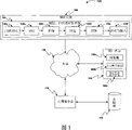
Fig. 1 is according to the specific embodiment of exemplary crystal grain tracker of the present invention;
Fig. 2 is according to the process flow diagram of the exemplary specific embodiment of crystal grain follow-up mechanism of the present invention;
Fig. 3 shows the exemplary die pick pattern of wafer;
Fig. 4 shows the example of the die pick order of wafer;
Fig. 5 be presented in the batch treatment with the crystal grain unit from a collection of be transferred to the preceding of another batch and after, batch in exemplary crystal grain data;
Fig. 6 be presented at one merge in the batch processing with the crystal grain unit from a collection of be transferred to the preceding of another batch and after, batch in exemplary crystal grain data;
Fig. 7 shows and to be used for one of the present invention exemplary graphical user (UI), and it is used for batch in order to appointment or the crystal grain ID of material operation;
Fig. 8 shows and to be used for another exemplary graphical user of the present invention, and it is used for batch in order to appointment or the crystal grain ID of material operation;
Fig. 9 demonstration is used for one of the present invention exemplary graphical user, and it is used to obtain the crystal grain trace information.
Embodiment
Specific embodiments of the invention provide a kind of crystal grain tracker, method and product, and it helps in manufacture process operating period tracking crystal grain unit, and a wherein for example a collection of part is transferred to another batch.Now please refer to accompanying drawing, and especially with reference to Fig. 1, it shows a crystal grain tracker 100, help when (for example) factory or approving and forwarding move to another, to follow the tracks of the crystal grain unit at material, and as a collection of transfer process in keep correspondence between crystal grain data and individual die effectively.System 100 can comprise that one or more manufacturing system 102, test/assembling and package system 104 (for example FLEXTM test macro of U.S. Ma Zhou Boston Teradyne company), mainframe network 106, user interface 108, application server 110 are (as the IBM WebSphere of the IBM Corporation of New York, United States Armonk
And database 112 (as the Oracle of the Oracle company of California, USA RedwoodShores) application server).Test/assembling and package system 104 can comprise in order to carry out relevant (for example) wafer sort 104a (as the APT system of the Keithley Instruments company of Ohio, USA Cleveland), stripping and slicing 104b (as the Dynatex wafer stripping and slicing system of the DynatexInternational of California, USA Santa Rosa), a bonding wire 104c (the Kulicke ﹠amp of U.S. Binzhou WillowGrove for example; Soffa), the operation of encapsulation 104d and test and burned 104e.To be easy to understand as those of ordinary skill in the art, and can contain any amount of different device and use to cooperate said system 100.
In the one or more specific embodiments of the present invention, application server 110 produces a unique crystal grain ID by the user at each crystal grain unit.Application server 110 is complied with one by one, and corresponded manner is assigned to the crystal grain unit with crystal grain ID.In another specific embodiment of the present invention, crystal grain ID is produced by manufacturing system 102.Crystal grain ID can be free form character string (crystal grain character string), its user definition or by using or instrument externally produces.The crystal grain ID that is produced is stored in the database 112.Being used for crystal grain ID a collection of or material crystal grain unit can save as one and be assigned to concatenation character string a collection of or material object (WIP object).In one example, crystal grain information can be assigned to the maximum WIP object that is associated with the carrier object (as, batch but not material).
Relevant individual die and the history thereof of following the tracks of when individual die is transmitted by manufacturing system 102 and in different WIP objects, one or more specific embodiments of the present invention consider that application program 110 meetings are to specifying a pointer character string from the crystal grain information of WIP object in source in the manufacturing system 102.For example, this pointer character string is the numerical range of the actual die unit in the given WIP object of expression.Each installs the data of the jump operation of the crystal grain unit of carrying out to manufacturing system 102 in by test, assembling and package system 104 to application server 110 transmission.In a particular instance, glutinous brilliant instrument 104c can provide about insert the information in individual leadframe frame or the draw-in groove from the crystal grain of which series of a wafer.Application server 110 receives this data via network 106, and specifies another pointer character string to give corresponding to the crystal grain information that is transferred to the crystal grain unit that receives the WIP object.In specific embodiments of the invention, all crystal grain information from source WIP object are copied into and receive the WIP object.Application server 110 will be corresponding to from the pointer character string of the crystal grain unit that source WIP object shifts, and connects with crystal grain information preface in receiving the WIP object, and the character string that produces is stored in the database 112.In addition, application server 110 is adjusted the pointer character string corresponding to crystal grain unit in the WIP object of source, with indication remaining crystal grain unit in the WIP object of this source, and the character string that produces is stored in the database 112.In this mode, system 100 follows the tracks of its history in a specific die when a WIP object is passed to another, and allows to pass through to adjust the pointer character string but not the common huger crystal grain information of adjustment, to shift crystal grain in the WIP object.
Fig. 2 (substantially 200) shows the illustrative methods according to exemplary specific embodiment of the present invention.In step 202, application server 110 is specified the unique string of individual die ID to the crystal grain unit in this batch or material object.In one embodiment, application server 110 is specified the successive range of crystal grain ID to this batch or material object.The crystal grain ID (and substantially by connecting crystal grain information) that is assigned to the WIP object by application server 110 can be from result's (for example providing from front-end equipment or by individual tool) of crystal grain figure input, and expection becomes the form that can discern uniquely.In a particular instance, glutinous brilliant instrument 104c can provide according to the crystal grain information of inserting the coordinate form of the interior crystal grain unit of wafer in individual leadframe frame or the draw-in groove.This crystal grain information can comprise absolute unique coordinate (as,<unique wafer ID〉_<Xm _<Yn,<unique wafer ID〉_<Xv _<Yw).
In the present invention's one or more alternative (and/or overlapping) property specific embodiment, this system's support can be attached to five extra matched character string of the crystal grain information of crystal grain ID.In one example, the number that mates the discrete crystal grain ID in crystal grain ID character string at the number of project described in each character string.The pointer character string that is assigned to crystal grain ID also is applied to the additional characters string that all have been attached to crystal grain ID.These additional characters strings allow the extra crystal grain information of user definition and need not additional data to discrete crystal grain ID.In fact, it provides the equivalent with 5 attribute column for each crystal grain ID.These character strings form one group of crystal grain data together with the pointer character string.The crystal grain data that are used for a collection of or material are stored in the concatenation character string of individual die ID together with the pointer character string of correspondence.Actual die or grain colony that these pointer indications are kept by this batch or material object.
In the present invention's one specific embodiment, when the wafer non-rectangle, crystal grain information comprises crystal grain figure, and it has by the pickup order data as glutinous brilliant instrument.Fig. 3 shows the exemplary die pick pattern that is used for a wafer.The die pick pattern decision of glutinous brilliant equipment is passed to the crystal grain ID tabulation of lead frame draw-in groove.Fig. 4 shows the example by the die pick order of the wafer of glutinous brilliant instrument.If the crystal grain information format is used this crystal grain information that comprises these crystal grain figure in scope the time, the crystal grain information that its expression is assigned to a WIP object does not have the discrete crystal grain ID that can directly obtain from database 112.In one example, pickup mode information stores by product type, and in another (or overlapping) example, pickup mode information stores by wafer size.
One or more specific embodiments of the present invention comprise a die pick race-card, and (and using it) stores the crystal grain coordinate model of the wafer of a product type.In one example, this die pick race-card can be used as a look-up table between between wafer coordinate scope and sequence numbering scope.In one example, if grain colony information provides as Serial Number Range, this look-up table helps to search actual coordinate.Table 1 shows the example of the die pick order that is used for wafer shown in Figure 4.When this table was used to search, the part according to the crystal grain ID character string of known UNC was removed by system.In one example, when searching " wafer23415_x24_y2 ", system will use " x24_y2 " part of crystal grain ID.For example, if glutinous brilliant equipment indication is shifted crystal grain unit 1 to 480 to lead frame draw-in groove " draw-in groove 101 " from wafer " wafer XYZ ", system obtains suitable pickup mode according to the product type of wafer.At scope 1 to 480, this system can obtain independent crystal grain ID (as being used for " WaferXYZ_x21_y1 " of the 1st crystal grain, " WaferXYZ_x22_y1 " of the 2nd crystal grain or the like) by wafer ID is connected with the coordinate of each order.The crystal grain data of " draw-in groove 101 " then be " WaferXYZ_x21_y1, WaferXYZ_x22_y1 ..., WaferXYZ_xn_ym ", and the pointer character string is " 1:480 ".
Table 1: die pick pattern list
| Crystal grain figure title | Order # | The crystal grain |
| Product_A_wafer_pattern | ||
| 1 | X21_y1 (the upper left | |
| | 2 | x22_y1 |
| | 3 | x23_y1 |
| | 4 | x24_y1 |
| ……… | … | … |
| Product_A_wafer_pattern | 37 | X57_y1 (the 1st row finishes crystal grain #37) |
| Product_A_wafer_pattern | 38 | X20_y1 (beginning the 2nd row crystal grain #38) |
| Product_A_wafer_pattern | 39 | x21_y2 |
| Product_A_wafer_pattern | 40 | x22_y2 |
| Product_A_wafer_pattern | 41 | x23_y2 |
| …… | … | … |
In one example, the sequence numbering of each coordinate can be in order to identification individual die ID after a separate processes in the table 1.As shown in table 1, this system can become the crystal grain information storage three parts: original coordinates range data, sequence numbering range data and crystal grain figure title.In one example, crystal grain information comprise the crystal grain character string (as, Wafer1_x1_y1:Wafer1_x3_y42), range data (as, 1:480) and crystal grain figure title (as, Product_A_wafer_pattern).
Still please refer to Fig. 2, at step 204 place, a pointer character string is specified in the crystal grain unit of application server 110 in the WIP object.In the present invention's one specific embodiment, the scope of crystal grain unit in the pointer string representation WIP object.At deciding step 206 places, whether system's decision is transferred to another with the crystal grain unit from a WIP object physics.Wherein the exemplary operation that the crystal grain unit is transferred to another from a WIP object comprises that record reduces, material divides into groups, removes material, terminal again and criticizes, adjusts batch and the fellow in a collection of batch separately and the merging, material transfer, same batch.If there is the crystal grain unit to be transferred to another from a WIP object physics, then at step 208 place, system receives WIP object copy crystal grain information to one.
In the present invention's one specific embodiment, the physical transfer of crystal grain unit occurs in the operating period that comprises a batch treatment.In another specific embodiment of the present invention, the physical transfer of crystal grain unit occurs in and comprises that a collection of merging handles operating period.In the specific embodiment of the present invention about a batch treatment, system can copy whole parent at step 208 place and criticize crystal grain information to filial generation and criticize.In the specific embodiment of the present invention about a union operation, this system can merge the crystal grain information of criticizing with all and incorporate in the target batch.Following example shows batch treatment:
The crystal grain information that parent is criticized separately
“lot34456-1.1_x34_y47,lot34456-1.1_x35_y47,lot34456-1.1_x1_y48,…,lot34456-1.2_x1_y1”
Range data (pointer character string)=1:5000
The user specifies and is transferred to the grain colony that filial generation is criticized:
Filial generation is criticized #1 and is received:
Crystal grain ID character string=" lot34456-1.1_x34_y47, lot34456-1.1_x35_y47, lot34456-1.1_x1_y48 ..., lot34456-1.2_x1_y1 " ← do not change
Range data=1:2500 ← the usable range of crystal grain in the pointer character string
Filial generation is criticized #2 and is received:
Crystal grain ID character string=" lot34456-1.1_x34_y47, lot34456-1.1_x35_y47, lot34456-1.1_x1_y48 ..., lot34456-1.2_x1_y1 " ← do not change
Range data=2501:5000 ← the usable range of crystal grain in the pointer character string
Separating the crystal grain data that the stepfather criticizes in generation:
" lot34456-1.1_x34_y47, lot34456-1.1_x35_y47, lot34456-1.1_x1_y48 ..., lot34456-1.2_x1_y1 " ← do not change
The usable range of crystal grain system is adjusted to zero in range data=0:0 ← character string
Therefore all crystal grains ID keeps identical, and only has the falsification of pointer character to become (as detailed below).
Please look back Fig. 2, at step 210 place, system will specify another pointer character string to transferring to the crystal grain unit that receives the WIP object.In the present invention's one specific embodiment, the pointer character string will be indicated and will be transferred to the crystal grain unit that receives the WIP object from source WIP object.At step 212 place, system will adjust the pointer character string that is assigned to residue crystal grain unit in the WIP object of source.In one example, the pointer character string is adjusted with indication and shifts remaining crystal grain unit in the WIP object of source, back.Fig. 5 and Fig. 6 be presented at the crystal grain unit from a WIP object be transferred to another (as, from batch separate processes of LOT1 to LOT2; Batch merging between LOT3 and LOT4 is handled) before and after, the exemplary crystal grain data in criticizing.
In the one or more specific embodiments of the present invention (and/or its situation), the physical transfer of crystal grain unit occurs in following operating period, these operations are included in the manufacturing system 102 moves contain the wafer casket a collection of by glutinous brilliant 104c and bonding equipment 104d, crystal grain is placed on the lead frame, and lead frame is placed the lead frame draw-in groove.In one example, can produce the material of one of expression lead frame draw-in groove.The crystal grain ID of this draw-in groove can be assigned to this material.In one example, crystal grain information comprises:
Crystal grain ID character string:<user-defined free-format crystal grain ID character string 〉
Additional characters string 1: the extra crystal grain information character of<user-defined free-format string 〉
Additional characters string 2: the extra crystal grain information character of<user-defined free-format string 〉
Additional characters string 3: the extra crystal grain information character of<user-defined free-format string 〉
Additional characters string 4: the extra crystal grain information character of<user-defined free-format string 〉
Additional characters string 5: the extra crystal grain information character of<user-defined free-format string 〉
Range data:<about the range data of crystal grain ID character string 〉
Crystal grain figure title: [option]<crystal grain figure title〉← the die pick order
For example:
For discrete crystal grain ID:
Crystal grain ID character string=" lot34456-1.1_x34_y47, lot34456-1.1_x35_y47 ..., lot34456-1.1_x1_y48, lot34456-1.2_x1_y1 "
Additional characters string 1:<lead frame 1, lead frame 1 ..., lead frame 40
Additional characters string 2:<position-1, position-1 ..., position-3
Additional characters string 3:<wafer-4, wafer-4 ..., wafer-5
Additional characters string 4:
Additional characters string 5:
Range data=1:480
Crystal grain figure title:
For the scope coordinate:
Crystal grain ID character string=" Wafer1_x1_y1:Wafer1_x3_y42 "
Additional characters string 1:<lead frame 1, lead frame 1 ..., lead frame 40
Additional characters string 2:<position-1, position-1 ..., position-3
Additional characters string 3:<wafer-4, wafer-4 ..., wafer-5
Additional characters string 4:
Additional characters string 5:
Range data: 1:480
Crystal grain figure title:<Product_A_wafer_pattern〉← the die pick order
These crystal grain ID data will be assigned to be criticized or the material object.
Fig. 7 shows and to be used to specify batch or the exemplary appointment crystal grain information UI of the crystal grain ID of material operation.During some batch or material operation of reducing, reach in batches material for transfer such as record, if selected batch or material have and specify crystal grain ID, system will provide a user interface to specify the crystal grain id information according to as shown in Figure 7 the scope or the form of individual die ID tabulation.In one example, when selected " appointment grain colony " option (as shown in Figure 7), the indication range that system allows the user to specify to be used for these crystal grain ID (as, crystal grain 1 to 480 enters draw-in groove _ 1 when material transfer is operated).In another example, when selected " specifying crystal grain ID tabulation " option (as shown in Figure 8), the Lower Half of UI can activate, and the tabulation of existing crystal grain ID is presented in " available crystal grain " tabulation.In another example, the user can be in tabulation selected individual die ID, or a scope is selected on the hurdle of tabulating since then and with its adding tabulation hurdle of " having specified crystal grain ".Simultaneously, as pointing out before that crystal grain ID can automatically be produced according to some standards and/or criterion by system.
In the one or more specific embodiments of the present invention, this system can be used for producing together with the crystal grain data of the crystal grain ID that comprises discrete scheme the history of a crystal grain unit.In one example, this system uses the UI shown in Fig. 9 to obtain the history of a crystal grain unit as follows:
1. start and search the historical UI of crystal grain and provide crystal grain ID and crowd ID (if available);
2. search the crystal grain history lists that is used for this crystal grain ID, it passes through:
(a) for an available crowd ID, obtain crystal grain ID character string according to the target batch object; The pointer position of decision specific die unit in this crystal grain ID character string; Use this crystal grain ID character string as search criteria, to obtain the WIP object that all comprise this crystal grain ID character string; And for obtaining each WIP object, whether the pointer range of checking WIP object comprises the pointer of this crystal grain unit.
(b), scan all WIP objects and check that its crystal grain ID character string is to mate this crystal grain ID for one disabled crowd of ID; The pointer position of decision specific die in this crystal grain ID character string; Use this crystal grain ID character string as search criteria, to obtain the WIP object that all comprise this crystal grain ID character string; And for acquired each WIP object, whether the pointer range of checking WIP object comprises the pointer of this crystal grain unit.
3. demonstration is from the history of the specific WIP object of the tabulation of the history that contains this WIP object, to show carrier and the equipment that is associated with this object.
Fig. 9 shows the historical UI of exemplary search crystal grain that is used to obtain the crystal grain trace information.This UI will allow to search the crystal grain trace information by importing a specific die ID and criticizing ID, to obtain trace information.This input comprises crystal grain ID (content that desire is searched): wafer1_x1_y1, and crowd ID; Crowd ID at present of chip.The user can select row and right button to be used for the historical ID of this object with startup.
Part of the present invention and corresponding detailed description system present with software, computer program or algorithm.Software comprises with the data bit form and is stored in the operation in the calculator memory or the symbolic notation of step.Algorithm is the order that causes demand result's step.These steps are the required content of the physical manipulation of physical quantity.Usually (but inessential) these quantity adopt can store, shift, in conjunction with, relatively or the light of handling, the form of electrical or magnetic signal.Unless specific separately point out or under discussion obviously as seen, refer to the action and the processing of computer system or similar computing electronics such as " processing " or " decision " or its similar noun, be rendered as the data of entity, amount of electrons in the internal memory of its manipulation and coordinate conversion computer system, become other data that are rendered as the entity amount in the internal memory of computer system or buffer or other these information storage, transmission or the display device equally.
Though above detailed description shows, describes and points out basic novel feature of the present invention for being applied to above-mentioned various specific embodiment, should be appreciated that those of ordinary skill in the art can form and the details to shown device carry out various omissions, substitute and change under the situation that does not break away from spirit of the present invention and category.With regard to each side, described specific embodiment should be regarded as only for exemplary and nonrestrictive.
Claims (37)
1, a kind of in order to follow the tracks of the method for crystal grain unit during manufacturing operation, it comprises following operation steps at least:
To specifying the first pointer character string with a plurality of one to one crystal grain character strings in a plurality of crystal grain unit, wherein this a plurality of crystal grain unit is relevant with a source object, and wherein each scope of the pointer that is comprised by the first pointer character string is discerned one of them of these a plurality of crystal grain character strings;
When at least some described crystal grain unit are transferred to one when receiving object from source object, a plurality of crystal grain character strings that will be associated with a plurality of crystal grain unit are copied to the reception object from source object;
The crystal grain character string that is associated with the crystal grain unit that is transferred to the reception object from source object is specified the second pointer character string, thereby indication has been transferred to the crystal grain unit that receives object;
Be adjusted at the first pointer character string in the source object to indicate remaining crystal grain unit in this source object.
2, method according to claim 1 is characterized in that, also comprises the step of described a plurality of crystal grain character strings being specified a plurality of user-defined character strings according to mode one to one.
3, method according to claim 1 is characterized in that, also comprises the operation steps of specifying a die pick order to described a plurality of crystal grain character strings according to mode one to one.
4, method according to claim 1, it is characterized in that, also comprise and store the described pointer character string relevant and the step of crystal grain character string, the history that pointer character string that has wherein stored and crystal grain character string are followed the tracks of these crystal grain unit with these crystal grain unit that are transferred to the reception object from source object.
5, method according to claim 4 is characterized in that, comprises that also generation one comprises the step of the report of crystal grain element keeps track information at least.
6, method according to claim 1 is characterized in that, described crystal grain character string comprises wafer ID and crystal grain coordinate.
7, method according to claim 1 is characterized in that, each crystal grain coordinate comprises an X coordinate and Y coordinate.
8, method according to claim 1 is characterized in that, each crystal grain character string comprises a wafer ID and a numerical order scope.
9, method according to claim 1 is characterized in that, described source object is a plurality of wafers, and described reception object is a plurality of lead frames.
10, method according to claim 1 is characterized in that, described source object is more than first lead frame, and described reception object is more than second draw-in groove.
11, method according to claim 1 is characterized in that, produces described crystal grain character string by a crystal grain figure of described source object.
12, a kind of in order to during manufacturing operation, to follow the trail of the method for crystal grain unit, comprise following steps at least:
Specify a plurality of crystal grain character strings and user's definition character string according to corresponding one to one uniquely to a plurality of crystal grain unit, wherein these a plurality of crystal grain unary systems and a source object associated;
Specify one first pointer character string to these a plurality of crystal grain character strings and user's definition character string, wherein each scope of the pointer that comprises by this first pointer character string can discern with these a plurality of crystal grain character strings of described crystal grain unit associated and user's definition character string in one of;
When at least some described crystal grain unit are transferred to one when receiving object from this source object, will be copied to a reception object from this source object with this a plurality of crystal grain character strings and user's definition character string of this a plurality of crystal grain unit associated;
The described crystal grain character string and the user's definition character string that are transferred to the described crystal grain unit associated of this reception object with this source object are certainly specified one second pointer character string, be transferred to the crystal grain unit of this reception object with indication; And
Be adjusted at this first pointer character string in this source object, to indicate remaining crystal grain unit in this source object.
13, method according to claim 12 is characterized in that, also comprises according to correspondingly described a plurality of crystal grain character strings being specified a die pick steps in order one to one.
14, method according to claim 12 is characterized in that, also comprises storing and the described pointer character string of the described crystal grain unit associated that is transferred to this reception object from this source object and the step of crystal grain character string.
15, method according to claim 12 is characterized in that, described crystal grain character string comprises wafer ID and crystal grain coordinate.
16, method according to claim 12 is characterized in that, each crystal grain coordinate comprises an X coordinate and Y coordinate.
17, method according to claim 12 is characterized in that, described crystal grain character string comprises a wafer ID and a numerical order scope.
18, method according to claim 12 is characterized in that, a plurality of wafers of this source object, and this reception object is a plurality of lead frames.
19, method according to claim 12 is characterized in that, this source object is a plurality of lead frames, and this reception object is a plurality of draw-in grooves.
20, method according to claim 12 is characterized in that, described crystal grain character string is to produce from a crystal grain figure of this source object.
21, a kind of in order to follow the trail of the system of crystal grain unit in manufacturing operation, it comprises at least:
One processor, it is in order to specify one first pointer character string to complying with corresponding one to one a plurality of crystal grain character strings of unique appointment of a crystal grain unit at the most, wherein this an a plurality of crystal grain unit and a source object associated, wherein each pointer in this first pointer character string one of can be discerned in these a plurality of crystal grain character strings;
One tracking mechanism, it is in order to follow the trail of at least some crystal grain unit that are transferred to a reception object from this source object, wherein this tracking mechanism:
To be copied to this reception object from this source object with at least some crystal grain character strings of the described crystal grain unit associated that has shifted;
The described crystal grain character string that is transferred to the described crystal grain unit associated of this reception object with this source object is certainly specified one second pointer character string; And
Be adjusted at this first pointer character string in this source object, to indicate remaining crystal grain unit in this source object.
22, method according to claim 21 is characterized in that, also comprises a glutinous brilliant machine, and it is used for producing the crystal grain character string from a crystal grain figure of this source object.
23, method according to claim 21 is characterized in that, also comprises a crystal grain through ephemeris, and it is in order to store and the pointer character string and the crystal grain character string that are transferred to the described crystal grain unit associated of this reception object from this source object.
24, a kind of in order to follow the tracks of the system of crystal grain unit in manufacturing operation, it comprises at least:
In order to specifying the device of the first pointer character string with a plurality of crystal grain character strings of a plurality of crystal grain unit unique appointment one to one, wherein this a plurality of crystal grain unit is associated with a source object, and wherein each pointer range that is comprised by the first pointer character string is discerned one in described a plurality of crystal grain character string;
In order to from source object when receiving object and shift at least some crystal grain unit, a plurality of crystal grain character strings that will be associated with this a plurality of crystal grain unit are copied to a device that receives object from source object;
In order to the crystal grain character string that is associated with the crystal grain unit of transferring to the reception object from source object is specified the device of the second pointer character string, transferred to the crystal grain unit that receives object with indication; And
In order to be adjusted at the device of the first pointer character string in the source object, to indicate remaining crystal grain unit in this source object.
25, system according to claim 24 is characterized in that, also comprises the device of described a plurality of crystal grain character strings being specified a plurality of user-defined character strings according to mode one to one.
26, system according to claim 24 is characterized in that, also comprises the device of specifying a die pick order to described a plurality of crystal grain character strings according to mode one to one.
27, system according to claim 24 is characterized in that, also comprises storing the pointer character string that is associated with these crystal grain unit that are transferred to the reception object from source object and the device of crystal grain character string.
28, system according to claim 24 is characterized in that, described crystal grain character string comprises wafer ID and crystal grain coordinate.
29, system according to claim 28 is characterized in that, each crystal grain coordinate comprises an X coordinate and Y coordinate.
30, system according to claim 24 is characterized in that, each crystal grain character string comprises a wafer ID and a numerical order scope.
31, system according to claim 24 is characterized in that, described source object is a plurality of wafers, and described reception object is a plurality of lead frames.
32, system according to claim 24 is characterized in that, described source object is more than first lead frame, and described reception object is a plurality of draw-in grooves.
33, system according to claim 24 is characterized in that, produces described crystal grain character string by a crystal grain figure of described source object.
34, a kind of computer program that resides on the computer-readable media, the instruction that this computer program comprises at least are with so that a computing machine carries out following action:
Specify one first pointer character string to complying with corresponding one to one a plurality of crystal grain character strings of only appointment of a crystal grain unit at the most, wherein this an a plurality of crystal grain unit and a source object associated, wherein each scope of the pointer that is comprised by this first pointer character string one of can be discerned in these a plurality of crystal grain character strings;
When at least some described crystal grain unit are transferred to one when receiving object from this source object, will be copied to a reception object from this source object with this a plurality of crystal grain character strings of this a plurality of crystal grain unit associated;
The described crystal grain character string that is transferred to the described crystal grain unit associated of this reception object with this source object is certainly specified one second pointer character string, be transferred to the crystal grain unit of this reception object with indication; And
Be adjusted at this first pointer character string in this source object, to indicate remaining crystal grain unit in this source object.
35, method according to claim 34 is characterized in that, it also comprises uses so that computing machine is complied with the instruction of correspondingly specifying a plurality of user's definition character strings one to one to described a plurality of crystal grain character strings.
36, method according to claim 34 is characterized in that, it also comprises uses so that computing machine is complied with the instruction of correspondingly specifying a die pick order one to one to described a plurality of crystal grain character strings.
37, method according to claim 34 is characterized in that, it also comprises uses so that computer stored and the described pointer character string of the described crystal grain unit associated that is transferred to this reception object from this source object and the instruction of crystal grain character string.
Applications Claiming Priority (2)
| Application Number | Priority Date | Filing Date | Title |
|---|---|---|---|
| US61880504P | 2004-10-15 | 2004-10-15 | |
| US60/618,805 | 2004-10-15 |
Publications (1)
| Publication Number | Publication Date |
|---|---|
| CN101040290A true CN101040290A (en) | 2007-09-19 |
Family
ID=35754092
Family Applications (1)
| Application Number | Title | Priority Date | Filing Date |
|---|---|---|---|
| CNA2005800352387A Pending CN101040290A (en) | 2004-10-15 | 2005-10-12 | Die-level traceability mechanism for semiconductor assembly and test facility |
Country Status (7)
| Country | Link |
|---|---|
| US (2) | US7343214B2 (en) |
| EP (1) | EP1810326A1 (en) |
| JP (1) | JP2008517465A (en) |
| KR (1) | KR20070085369A (en) |
| CN (1) | CN101040290A (en) |
| TW (1) | TW200629026A (en) |
| WO (1) | WO2006044399A1 (en) |
Families Citing this family (9)
| Publication number | Priority date | Publication date | Assignee | Title |
|---|---|---|---|---|
| GB0800227D0 (en) * | 2008-01-07 | 2008-02-13 | Metryx Ltd | Method of controlling semiconductor device fabrication |
| TWI442401B (en) * | 2009-12-30 | 2014-06-21 | Macronix Int Co Ltd | 3d chip select for sheard input packages |
| KR101575831B1 (en) | 2010-10-04 | 2015-12-08 | 샌디스크 세미컨덕터 (상하이) 컴퍼니, 리미티드 | Discrete component backward traceability and semiconductor device forward traceability |
| US9559113B2 (en) | 2014-05-01 | 2017-01-31 | Macronix International Co., Ltd. | SSL/GSL gate oxide in 3D vertical channel NAND |
| KR20160018227A (en) * | 2014-08-08 | 2016-02-17 | 에스케이하이닉스 주식회사 | System for Processing Wafer and Method of Processing Wafer Using The Same |
| US10419410B2 (en) * | 2016-12-15 | 2019-09-17 | Seagate Technology Llc | Automatic generation of unique identifiers for distributed directory management users |
| KR102653937B1 (en) | 2018-07-17 | 2024-04-02 | 삼성전자주식회사 | Test method for semiconductor devices and test system for semiconductor devices |
| US11063000B2 (en) * | 2019-01-29 | 2021-07-13 | Infineon Technologies Ag | Semiconductor package authentication feature |
| US11450616B2 (en) | 2020-07-29 | 2022-09-20 | Nxp Usa, Inc. | Using a backside mask layer for forming a unique die mark identifier pattern |
Family Cites Families (83)
| Publication number | Priority date | Publication date | Assignee | Title |
|---|---|---|---|---|
| US17708A (en) * | 1857-06-30 | Coloring yarn ijst the bobbin | ||
| US21265A (en) * | 1858-08-24 | Improvement in rotary harrows | ||
| US256463A (en) * | 1882-04-18 | Journal-bearing | ||
| US5090A (en) * | 1847-05-01 | Improvement in diffusers for water-wheels | ||
| US34785A (en) * | 1862-03-25 | Improvement in heaters | ||
| US103628A (en) * | 1870-05-31 | Lemuel w | ||
| US76897A (en) * | 1868-04-21 | Improved composition foe blacking leatheb | ||
| US176872A (en) * | 1876-05-02 | Improvement in gang-planks | ||
| US157762A (en) * | 1874-12-15 | Improvement in bird-cages | ||
| US224540A (en) * | 1880-02-17 | Caleb h | ||
| US36677A (en) * | 1862-10-14 | Improvement in hoop-skirts | ||
| US4767A (en) * | 1846-09-19 | Pike-engine | ||
| US95172A (en) * | 1869-09-21 | Improved shoemakers tool | ||
| US42780A (en) * | 1864-05-17 | Improvement in wood-splitting machines | ||
| US251472A (en) * | 1881-12-27 | sohmetzer | ||
| US187737A (en) * | 1877-02-27 | Improvement in mowing-machines | ||
| US744A (en) * | 1838-05-17 | Mode of cutting off steam in steam-engines | ||
| US26949A (en) * | 1860-01-24 | William lewis | ||
| US141605A (en) * | 1873-08-05 | Improvement in packages for fruit | ||
| US62609A (en) * | 1867-03-05 | Improved life-pbeservdfg beeth | ||
| US6404A (en) * | 1849-05-01 | shaw and ezra gould | ||
| US132060A (en) * | 1872-10-08 | Improvement in windmills | ||
| US225385A (en) * | 1880-03-09 | Service-pipe box | ||
| US38779A (en) * | 1863-06-02 | Improvement in thrashing-machines | ||
| US87113A (en) * | 1869-02-23 | Improvement in reel and swift | ||
| US158795A (en) * | 1875-01-19 | Improvement in clover-harvesters | ||
| US203591A (en) * | 1878-05-14 | Improvement in tools for trimming and finishing the edges of dash-boards | ||
| US124437A (en) * | 1872-03-12 | Improvement in type writing-machines | ||
| US106931A (en) * | 1870-08-30 | Improvement in machine for rounding fellies for wheels | ||
| US81756A (en) * | 1868-09-01 | Improved traveling-trunk | ||
| US183884A (en) * | 1876-10-31 | Improvement in gas-carbureters | ||
| US110270A (en) * | 1870-12-20 | Improvement in machines for making cigars | ||
| US5129974A (en) * | 1990-08-23 | 1992-07-14 | Colorcode Unlimited Corporation | Microlabelling system and method of making thin labels |
| JPH07123101B2 (en) | 1990-09-14 | 1995-12-25 | 株式会社東芝 | Semiconductor device |
| US5625816A (en) * | 1994-04-05 | 1997-04-29 | Advanced Micro Devices, Inc. | Method and system for generating product performance history |
| US6941556B1 (en) | 1995-03-24 | 2005-09-06 | Sun Microsystems, Inc. | Method and system for type identification for multiple object interfaces in a distributed object environment |
| US5726920A (en) * | 1995-09-29 | 1998-03-10 | Advanced Micro Devices, Inc. | Watchdog system having data differentiating means for use in monitoring of semiconductor wafer testing line |
| US5751581A (en) * | 1995-11-13 | 1998-05-12 | Advanced Micro Devices | Material movement server |
| US5838361A (en) | 1996-01-11 | 1998-11-17 | Micron Technology, Inc. | Laser marking techniques |
| DE19640425A1 (en) | 1996-09-30 | 1998-04-02 | Siemens Ag | Process for wafer identification in chip production and device for carrying out the process |
| US6259960B1 (en) * | 1996-11-01 | 2001-07-10 | Joel Ltd. | Part-inspecting system |
| US6100486A (en) | 1998-08-13 | 2000-08-08 | Micron Technology, Inc. | Method for sorting integrated circuit devices |
| US6065113A (en) * | 1997-03-07 | 2000-05-16 | Texas Instruments Incorporated | Circuits, systems, and methods for uniquely identifying a microprocessor at the instruction set level employing one-time programmable register |
| US5856923A (en) | 1997-03-24 | 1999-01-05 | Micron Technology, Inc. | Method for continuous, non lot-based integrated circuit manufacturing |
| JPH1126333A (en) * | 1997-06-27 | 1999-01-29 | Oki Electric Ind Co Ltd | Semiconductor device and information control system thereof |
| US6446017B1 (en) | 1997-08-21 | 2002-09-03 | Micron Technology, Inc. | Method and system for tracking manufacturing data for integrated circuit parts |
| JP3394895B2 (en) | 1997-09-08 | 2003-04-07 | 沖電気工業株式会社 | Semiconductor storage device and method of manufacturing the same |
| US6128588A (en) * | 1997-10-01 | 2000-10-03 | Sony Corporation | Integrated wafer fab time standard (machine tact) database |
| US6216055B1 (en) * | 1997-12-16 | 2001-04-10 | Texas Instruments Incorporated | Partial semiconductor wafer processing |
| KR19990065486A (en) * | 1998-01-14 | 1999-08-05 | 윤종용 | Process Condition Management Method of Semiconductor Manufacturing Equipment Management System |
| US6049624A (en) * | 1998-02-20 | 2000-04-11 | Micron Technology, Inc. | Non-lot based method for assembling integrated circuit devices |
| US6268641B1 (en) | 1998-03-30 | 2001-07-31 | Kabushiki Kaisha Toshiba | Semiconductor wafer having identification indication and method of manufacturing the same |
| WO2000014790A1 (en) * | 1998-09-03 | 2000-03-16 | Hitachi, Ltd. | Inspection system and method for producing electronic device by using the same |
| KR100610175B1 (en) | 1999-03-24 | 2006-08-09 | 후지쯔 가부시끼가이샤 | Method for manufacturing a semiconductor device and method for writing chip identification information |
| US6337122B1 (en) | 2000-01-11 | 2002-01-08 | Micron Technology, Inc. | Stereolithographically marked semiconductors devices and methods |
| JP3555859B2 (en) | 2000-03-27 | 2004-08-18 | 広島日本電気株式会社 | Semiconductor production system and semiconductor device production method |
| US6792563B1 (en) | 2000-04-28 | 2004-09-14 | Intel Corporation | Method and apparatus for bus activity tracking |
| US6673692B2 (en) | 2000-06-28 | 2004-01-06 | Micron Technology, Inc. | Method and apparatus for marking microelectronic dies and microelectronic devices |
| JP3578057B2 (en) | 2000-07-06 | 2004-10-20 | 株式会社日立製作所 | ID management system |
| US6568593B2 (en) * | 2000-07-14 | 2003-05-27 | Trumpf Gmbh + Co. | System and method for identification of tools and parts of tools for a fabricating machine |
| US6351684B1 (en) * | 2000-09-19 | 2002-02-26 | Advanced Micro Devices, Inc. | Mask identification database server |
| JP2002184872A (en) | 2000-12-15 | 2002-06-28 | Hitachi Ltd | Semiconductor device with identification number, manufacturing method thereof, and electronic device |
| JP2002190509A (en) | 2000-12-22 | 2002-07-05 | Mitsubishi Electric Corp | Inspection analysis method and semiconductor device |
| US7031791B1 (en) * | 2001-02-27 | 2006-04-18 | Cypress Semiconductor Corp. | Method and system for a reject management protocol within a back-end integrated circuit manufacturing process |
| TW594590B (en) * | 2001-03-16 | 2004-06-21 | Taiwan Semiconductor Mfg | Split lot ID encoding system and method |
| US7100826B1 (en) * | 2001-03-26 | 2006-09-05 | Advanced Micro Devices, Inc. | Barcode marking of wafer products for inventory control |
| US6792365B2 (en) | 2001-08-10 | 2004-09-14 | Micron Technology, Inc. | Sequential unique marking |
| US6555400B2 (en) * | 2001-08-22 | 2003-04-29 | Micron Technology, Inc. | Method for substrate mapping |
| JP2003115424A (en) | 2001-10-03 | 2003-04-18 | Nec Corp | Semiconductor device, its identifying method, and semiconductor device manufacturing device |
| EP1391853A1 (en) | 2001-11-30 | 2004-02-25 | STMicroelectronics S.A. | Diversification of the unique identifier of an integrated circuit |
| US6616034B2 (en) | 2001-12-10 | 2003-09-09 | Fortrend Taiwan Scientific Corporation | Radio frequency identification device |
| US7035877B2 (en) | 2001-12-28 | 2006-04-25 | Kimberly-Clark Worldwide, Inc. | Quality management and intelligent manufacturing with labels and smart tags in event-based product manufacturing |
| US20030141605A1 (en) | 2002-01-25 | 2003-07-31 | Silicon Integrated Systems Corp. | Method of forming identifying mark on semiconductor wafer |
| JP4256115B2 (en) | 2002-05-28 | 2009-04-22 | 富士通マイクロエレクトロニクス株式会社 | Mark recognition method and semiconductor device manufacturing method |
| US6952623B2 (en) | 2002-07-02 | 2005-10-04 | Texas Instruments, Inc. | Permanent chip ID using FeRAM |
| US20040034785A1 (en) | 2002-08-15 | 2004-02-19 | Horng-Ming Tai | Hardware and firmware encryption mechanism using unique chip die identification |
| US6974761B2 (en) | 2002-09-27 | 2005-12-13 | Oki Electric Industry Co. | Method of forming a semiconductor laser chip having a marker |
| US6839601B1 (en) | 2002-11-26 | 2005-01-04 | Advanced Micro Devices, Inc. | Fabrication architecture including enterprise resource planning integration |
| US6812477B2 (en) | 2002-12-04 | 2004-11-02 | Texas Instruments Incorporated | Integrated circuit identification |
| US7015795B2 (en) | 2002-12-30 | 2006-03-21 | Potomac Photonics, Inc. | Self-identifying integrated circuits and method for fabrication thereof |
| US6959229B2 (en) | 2003-03-07 | 2005-10-25 | Sdi Industries, Inc. | RFID control system |
| US20040251472A1 (en) | 2003-06-11 | 2004-12-16 | Broadcom Corporation | Memory cell for modification of revision identifier in an integrated circuit chip |
| US7415317B2 (en) | 2004-02-25 | 2008-08-19 | Micron Technology, Inc. | Method and system for correlating and combining production and non-production data for analysis |
-
2005
- 2005-10-12 US US11/247,196 patent/US7343214B2/en not_active Expired - Fee Related
- 2005-10-12 WO PCT/US2005/036548 patent/WO2006044399A1/en active Application Filing
- 2005-10-12 CN CNA2005800352387A patent/CN101040290A/en active Pending
- 2005-10-12 KR KR1020077011038A patent/KR20070085369A/en not_active Application Discontinuation
- 2005-10-12 EP EP05804118A patent/EP1810326A1/en not_active Withdrawn
- 2005-10-12 JP JP2007536813A patent/JP2008517465A/en not_active Withdrawn
- 2005-10-14 TW TW094136036A patent/TW200629026A/en unknown
-
2007
- 2007-10-31 US US11/982,163 patent/US20080071413A1/en not_active Abandoned
Also Published As
| Publication number | Publication date |
|---|---|
| US7343214B2 (en) | 2008-03-11 |
| KR20070085369A (en) | 2007-08-27 |
| US20080071413A1 (en) | 2008-03-20 |
| TW200629026A (en) | 2006-08-16 |
| EP1810326A1 (en) | 2007-07-25 |
| JP2008517465A (en) | 2008-05-22 |
| US20060085089A1 (en) | 2006-04-20 |
| WO2006044399A1 (en) | 2006-04-27 |
Similar Documents
| Publication | Publication Date | Title |
|---|---|---|
| CN101040290A (en) | Die-level traceability mechanism for semiconductor assembly and test facility | |
| CN1254768C (en) | Part recognition data creation method and apparatus, electronic part mounting apparatus and recorded medium | |
| CN1215415C (en) | Files management method and storage information reproducing device and storage information recording medium | |
| CN1392954A (en) | Defect knowledge library | |
| CN1744116A (en) | System and method for semiconductor manufacturing automation | |
| CN1216403C (en) | Exposure method | |
| CN1647076A (en) | Method and apparatus for querying relational databases | |
| CN1556482A (en) | Data processing method for realizing data base multitable inguiry | |
| CN1315017A (en) | Difference extraction between two versions of data-tables containing intra-reference | |
| CN1171389C (en) | Parallet CRC generation circuit for generating a CRC code | |
| CN1208858A (en) | Semiconductor device test system with operation loss reduced | |
| CN1591425A (en) | Method for generating web site navigations | |
| JP2003324043A (en) | Semiconductor wafer manufacture execution system having recipe distribution managing data base | |
| CN1829279A (en) | Method for managing display device signal source | |
| CN1748153A (en) | Boundary scan controller, semiconductor device, method for identifying semiconductor circuit chip of semiconductor device, and method for controlling semiconductor circuit chip of semiconductor device | |
| CN1770165A (en) | A method and system for conducting an online transaction on multi-project wafer service | |
| CN1702659A (en) | IP base LSI designing system and designing method | |
| CN1211178C (en) | System and method for reducing welding program error for IC welding machine | |
| CN1161676C (en) | Process for determining possible configurations of machining plant | |
| CN1506883A (en) | Crosstalk detecting method | |
| CN1956005A (en) | Data access apparatus and method | |
| CN1047417C (en) | Apparatus and method for creating and modifying stitching data used by a sewing machine | |
| CN1147051C (en) | Error protecting method and error protective device | |
| CN100341028C (en) | Pattern segmentation device and pattern recognition device | |
| CN1410859A (en) | Semiconductor IC device with clock signal transmission line |
Legal Events
| Date | Code | Title | Description |
|---|---|---|---|
| C06 | Publication | ||
| PB01 | Publication | ||
| C10 | Entry into substantive examination | ||
| SE01 | Entry into force of request for substantive examination | ||
| C02 | Deemed withdrawal of patent application after publication (patent law 2001) | ||
| WD01 | Invention patent application deemed withdrawn after publication |
Open date: 20070919 |