KR20070015074A - Storage device, computer system, and storage system - Google Patents
Storage device, computer system, and storage system Download PDFInfo
- Publication number
- KR20070015074A KR20070015074A KR1020060071459A KR20060071459A KR20070015074A KR 20070015074 A KR20070015074 A KR 20070015074A KR 1020060071459 A KR1020060071459 A KR 1020060071459A KR 20060071459 A KR20060071459 A KR 20060071459A KR 20070015074 A KR20070015074 A KR 20070015074A
- Authority
- KR
- South Korea
- Prior art keywords
- memory
- area
- data
- page
- recovery process
- Prior art date
Links
Images


Classifications
-
- G—PHYSICS
- G06—COMPUTING; CALCULATING OR COUNTING
- G06F—ELECTRIC DIGITAL DATA PROCESSING
- G06F12/00—Accessing, addressing or allocating within memory systems or architectures
- G06F12/16—Protection against loss of memory contents
-
- G—PHYSICS
- G06—COMPUTING; CALCULATING OR COUNTING
- G06F—ELECTRIC DIGITAL DATA PROCESSING
- G06F12/00—Accessing, addressing or allocating within memory systems or architectures
- G06F12/02—Addressing or allocation; Relocation
- G06F12/0223—User address space allocation, e.g. contiguous or non contiguous base addressing
- G06F12/023—Free address space management
- G06F12/0238—Memory management in non-volatile memory, e.g. resistive RAM or ferroelectric memory
- G06F12/0246—Memory management in non-volatile memory, e.g. resistive RAM or ferroelectric memory in block erasable memory, e.g. flash memory
-
- G—PHYSICS
- G06—COMPUTING; CALCULATING OR COUNTING
- G06F—ELECTRIC DIGITAL DATA PROCESSING
- G06F12/00—Accessing, addressing or allocating within memory systems or architectures
-
- G—PHYSICS
- G06—COMPUTING; CALCULATING OR COUNTING
- G06F—ELECTRIC DIGITAL DATA PROCESSING
- G06F2212/00—Indexing scheme relating to accessing, addressing or allocation within memory systems or architectures
- G06F2212/72—Details relating to flash memory management
- G06F2212/7205—Cleaning, compaction, garbage collection, erase control
Landscapes
- Engineering & Computer Science (AREA)
- Theoretical Computer Science (AREA)
- Physics & Mathematics (AREA)
- General Engineering & Computer Science (AREA)
- General Physics & Mathematics (AREA)
- Techniques For Improving Reliability Of Storages (AREA)
- Read Only Memory (AREA)
- Memory System (AREA)
Abstract
Description
도 1은, NAND형 플래쉬 메모리의 내부 구성예를 나타내는 도면이다.1 is a diagram illustrating an internal configuration example of a NAND flash memory.
도 2는, 기억장치를 구성하는 플래쉬 메모리의 개념도를 나타내는 도면이다.2 is a diagram illustrating a conceptual diagram of a flash memory constituting a storage device.
도 3a, 및 도 3b는, 예를 들어 소거 블록내의 1페이지만을 고쳐 쓸 때의 순서의 일례를 설명하기 위한 도면이다.3A and 3B are diagrams for explaining an example of a procedure when rewriting only one page in an erase block, for example.
도 4a, 및 도 4b는, 어드레스 변환 테이블을 이용한 추기형(additional rewriting) 기억 시스템에 있어서의 관리 방법의 일례를 설명하기 위한 도면이다.4A and 4B are diagrams for explaining an example of a management method in an additional rewriting memory system using an address translation table.
도 5는, 제 1의 실시 형태와 관련되는 기억장치를 나타내는 구성도이다.5 is a configuration diagram showing a storage device according to the first embodiment.
도 6a, 6b는, 제 1의 실시 형태와 관련되는 제어 회로의 어드레스 변환 테이블 및 페이지 상태의 관리 테이블의 구성예를 나타내는 도면이다.6A and 6B are diagrams showing an example of the configuration of an address conversion table and a page state management table of the control circuit according to the first embodiment.
도 7a - 도 7c는 제 1의 실시 형태의 무효 영역의 회복 순서를 설명하기 위한 도면이다.7A to 7C are diagrams for explaining the recovery procedure of the invalid area in the first embodiment.
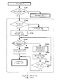
도 8은, 제 1의 실시 형태의 장치가 회복 처리를 실행하는 제어 순서의 예를 나타내는 플로차트(flow chart)이다.8 is a flowchart showing an example of a control procedure in which the apparatus of the first embodiment executes a recovery process.
도 9는, 제 1의 실시 형태의 변형예이며, 무효 페이지 영역 회복의 분할 단위 처리를 설명하기 위한 플로차트이다.9 is a modified example of the first embodiment, and is a flowchart for explaining the division unit processing for invalid page area recovery.
도 10은, 제 2의 실시 형태와 관련되는 회복 처리를 설명하기 위한 플로차트이다.10 is a flowchart for explaining a recovery process according to the second embodiment.
도 11은, 제 2의 실시 형태의 변형예이며, 무효 페이지 영역 회복의 분할 단위 처리를 설명하기 위한 플로차트이다.11 is a modification of the second embodiment, and is a flowchart for explaining the division unit processing for invalid page area recovery.
도 12는, 제 3의 실시 형태와 관련되는 기억장치를 나타내는 구성도이다.12 is a configuration diagram showing a storage device according to the third embodiment.
도 13은, 제 3의 실시 형태와 관련되는 제어 회로의 어드레스 변환 테이블의 구성예를 나타내는 도면이다.FIG. 13 is a diagram illustrating a configuration example of an address conversion table of a control circuit according to the third embodiment. FIG.
도 14는, 제 3의 실시 형태와 관련되는 회복 처리를 설명하기 위한 플로차트이다.14 is a flowchart for explaining a recovery process according to the third embodiment.
도 15는, 제 3의 실시 형태의 변형예이며, 무효 페이지 영역 회복의 분할 단위 처리를 설명하기 위한 플로차트이다.15 is a modified example of the third embodiment, and is a flowchart for explaining the division unit processing for invalid page area recovery.
도 16은, 제 3의 실시 형태의 제 2의 변형예이며, 무효 페이지 영역 회복의 분할 단위 처리를 설명하기 위한 플로차트이다.FIG. 16 is a second modification example of the third embodiment, and is a flowchart for explaining the division unit processing for invalid page area recovery.
도 17은, 제 4의 실시 형태에 있어서의 무효 영역의 회복 처리를 설명하기 위한 플로차트이다.FIG. 17 is a flowchart for explaining a recovery process of an invalid area in the fourth embodiment.
도 18은, 제 5의 실시 형태와 관련되는 컴퓨터 시스템의 구성예를 나타내는 도면이다.18 is a diagram illustrating a configuration example of a computer system according to the fifth embodiment.
도 19는, 제 5의 실시 형태와 관련되는 제어 회로의 어드레스 변환 테이블의 구성예를 나타내는 도면이다.19 is a diagram illustrating a configuration example of an address conversion table of a control circuit according to the fifth embodiment.
도 20은, 프리엠프티브(preemptive)한 멀티태스킹 시스템을 이용한 회복 처 리의 일례를 나타내는 플로차트이다.20 is a flowchart showing an example of recovery processing using a preemptive multitasking system.
도 21은, 제 6의 실시 형태를 나타내는 도이며, 그러한 ECC 처리와 결함 블록 관리를 도입한, 제 3의 실시 형태(도 12)의 장치 구성상의 응용 변형예를 나타내는 도면이다.FIG. 21 is a diagram illustrating a sixth embodiment and illustrates an application modification example of the apparatus configuration of the third embodiment (FIG. 12) incorporating such ECC processing and defective block management.
도 22a, 및 도 22b는, 제 6의 실시 형태와 관련되는 제어 회로의 어드레스 변환 테이블 및 페이지 상태의 관리 테이블의 구성예를 나타내는 도면이다.22A and 22B are diagrams showing an example of the configuration of an address conversion table and a page state management table of the control circuit according to the sixth embodiment.
도 23은, 제 7의 실시 형태와 관련되는 컴퓨터 시스템(기억 시스템)의 구성예를 나타내는 도면이다.FIG. 23 is a diagram showing an example of the configuration of a computer system (storage system) according to the seventh embodiment.
도 24는, 제 7의 실시 형태와 관련되는 제어 회로의 어드레스 변환 테이블 및 주소 검색 테이블의 구성예를 나타내는 도면이다.24 is a diagram illustrating a configuration example of an address conversion table and an address search table of a control circuit according to the seventh embodiment.
도 25는, 도 24의 어드레스 변환 테이블 및 검색 테이블을 사용한 데이터 액세스 처리를 설명하기 위한 플로차트이다.FIG. 25 is a flowchart for explaining data access processing using the address translation table and lookup table in FIG. 24.
도 26a - 도 26c는, 제 7의 실시 형태와 관련되는 무효 영역의 회복 순서를 설명하기 위한 도면이다.26A to 26C are diagrams for explaining a recovery procedure of an invalid area according to the seventh embodiment.
도 27은, 제 7의 실시 형태에 있어서의 구체적인 회복 처리를 설명하기 위한 플로차트이다.27 is a flowchart for explaining the specific recovery processing in the seventh embodiment.
도 28은, 제 8의 실시 형태와 관련되는 컴퓨터 시스템의 구성예를 나타내는 도면이다.FIG. 28 is a diagram illustrating a configuration example of a computer system according to an eighth embodiment.
본 발명은 2005년 7월 29일 일본 특허청에 제출된 2005-221714호와, 2006년 5월 17일 제출된 2006-137844호에 기술된 주제와 관련되며, 그 내용은 본 발명에 참조로서 포함되어 있다. The present invention relates to the subject matter described in 2005-221714, filed with the Japan Patent Office on July 29, 2005, and 2006-137844, filed on May 17, 2006, the contents of which are incorporated herein by reference. have.
본 발명은, 불휘발성 메모리를 포함한 기억장치 및 그것을 갖춘 컴퓨터 시스템, 및 기억 시스템에 관한 것이며, 특히 플래쉬 메모리를 포함한 기억장치에 있어서의 데이터 전송의 고속화에 관련되는 것이다.BACKGROUND OF THE
근년, 디지털 카메라나 모바일 컴퓨터 기기의 기억 매체로서 플래쉬 메모리가 주목받고 있다.In recent years, flash memory has attracted attention as a storage medium of digital cameras and mobile computer devices.
플래쉬 메모리는, 터널링이나 핫 일렉트론 가속을 이용하고, 전자에 게이트 절연막을 통과시켜, 그것들을 부유 게이트나 트랩층에 주입해, 셀 트랜지스터의 반응을 일으키는 최소의 물리량을 변화시키는 것으로서 데이터를 기억시키는 반도체 메모리이다. 적층 게이트 구조나 MNOS 구조등을 이용한 트랜지스터 1개만으로 메모리 셀을 구성할 수 있기 때문에, 염가이고 대용량의 메모리를 실현할 수 있다. 그 대표예로서 NAND형 플래쉬 메모리를 들 수 있다.A flash memory uses tunneling or hot electron acceleration to pass electrons through a gate insulating film, injects them into a floating gate or a trap layer, and stores the data by changing a minimum physical quantity that causes a cell transistor to react. Memory. Since a memory cell can be formed by only one transistor using a stacked gate structure, an MNOS structure, or the like, a low-capacity and large-capacity memory can be realized. A representative example thereof is a NAND flash memory.
도 1은, NAND형 플래쉬 메모리의 내부 구성예를 나타내는 도면이다.도 1의 NAND형 플래쉬 메모리는, 비트선(BL1~BLn)에 접속된 복수의 메모리유닛트(1-1~1-n)가 어레이 상태(종횡)로 배열되어 있다. 예를 들어, 선택용 트랜지스터(2)의 게이트가 선택 게이트선(SL1)에 접속되며 선택용 트랜지스터(3)의 게이트가 선택 게이트선(SL2)에 접속되어 있다. 또한, 각 메모리 셀(N0~N15)의 게이트가 워드 라인(WL0~WL15)에 접속되어 있다.Fig. 1 is a diagram showing an internal configuration example of a NAND flash memory. In the NAND flash memory of Fig. 1, a plurality of memory units 1-1 to 1-n connected to bit lines BL1 to BLn are shown. It is arranged in the array state (vertical and horizontal). For example, the gate of the
각 메모리 셀(N0~N15)은 적층 게이트 구조를 가지며, 부유 게이트내에 저장된 전하 축적량에 따라서 데이터를 기억한다. 즉, 부유 게이트에 많은 전자가 축적되어 있으면, 트랜지스터의 반응을 일으키는 최소의 물리량이 상승하므로, 충전된 비트선(BL1~BLn)으로부터 메모리 유닛트(1)(-1에서 -n까지)에 이르는 전류 관통이, 센스 증폭기등을 포함한 액세스 회로(4)에서 검출되어 데이터 판정을 가능하게 한다. Each memory cell N0 to N15 has a stacked gate structure and stores data according to the amount of charge stored in the floating gate. In other words, when a large amount of electrons are accumulated in the floating gate, the minimum physical amount causing the transistor to react increases, so that the current from the charged bit lines BL1 to BLn to the memory unit 1 (-1 to -n) is increased. Penetration is detected in an access circuit 4 including a sense amplifier or the like to enable data determination.
이러한 NAND형 플래쉬 메모리는, 메모리 셀마다 비트선에 컨택트 영역을 마련할 필요도 없기 때문에, 특히 대용량으로 염가의 기억장치의 매체에 적절하다.Such a NAND type flash memory does not need to provide a contact region on a bit line for each memory cell, and therefore is particularly suitable for a medium of a cheap storage device with a large capacity.
일반적으로 플래쉬 메모리의 프로그램 속도는 매우 늦고, 셀 당 수백μ 초를 필요로 한다. 또한 데이터의 오버라이팅(overwriting)을 할 수 없기 때문에, 프로그램에 앞서 데이터 소거를 실시할 필요가 있으므로, 이에 대해 수밀리(m) 초의 시간이 걸린다. 이러한 문제에 대해서는, 많은 메모리 셀을 병렬처리 하는 것으로 대처하고 있다.In general, the programming speed of flash memory is very slow and requires several hundred microseconds per cell. In addition, since data overwriting cannot be performed, it is necessary to perform data erasing prior to the program, which takes several milliseconds. This problem is addressed by parallelizing many memory cells.
즉, 예를 들어 동일 워드라인(WL0)에 접속되어 페이지 단위를 이루는 메모리 셀군(5)내에 동시에 블록 단위로 데이터를 기입하고, 서로 메모리 유닛트를 공유하는 페이지군으로 구성되는 셀 블록(6)을 블록 단위로 모두 소거함으로써 프로그램의 전송 속도를 향상시키고 있다.That is, for example, a cell block 6 composed of page groups which are connected to the same word line WL0 and write data in block units simultaneously in a
구체적으로는, 예를 들어 ISSCC2002 프리프린트 p106, 세션 6.4에는, 1Gb의 NAND형 플래쉬 메모리가 게재되어 있으며, 페이지 사이즈를 2k 바이트, 소거 블록 사이즈를 128kB로 하고 있다. 즉, 하나의 메모리 어레이내에서 128k바이트의 메모리 셀군을 병렬 소거하고, 거기에 메모리 셀을 2k바이트마다 병렬로 프로그래밍함으로써, 10MB/s의 프로그램 전송 속도를 실현하고 있다.Specifically, for example, a 1 Gb NAND flash memory is placed in the ISSCC2002 preprint p106 and the session 6.4, and the page size is 2k bytes and the erase block size is 128kB. In other words, a program transfer rate of 10 MB / s is realized by parallel erasing a 128k-byte memory cell group in one memory array and programming the memory cells in parallel every 2k bytes therein.
또한, 근년 플래쉬 메모리는 더욱 멀티값(multi-value)을 가지도록 설계되고 미세화가 진행되고 있으므로, 거기에 따르는 신호량의 저하에 대처하기 위해, 비선택 셀의 악영향이 적은 기입 수법이 검토되어 실시되고 있다.In addition, in recent years, since flash memories are designed to have more multi-values and are being miniaturized, in order to cope with a drop in the amount of signals accompanying them, a write method with less adverse effects of unselected cells is examined and implemented. It is becoming.
예를 들어 NAND형 플래시에 대해서는, 소거 블록내의 페이지의 기입순서에도 제한을 두는 것이 주류가 되고 있다. 일본 특개 2002-260390호 공보에는 그 하나로서 로컬 셀프 부스트(Local Self-Boost)로 불리는 수법을 이용한 기입 순서가 기재되어 있다. 도 1의 NAND형 플래쉬 메모리내의 그러한 기입의 예를 이하에 설명한다.For example, in the NAND type flash, the main limitation is to limit the writing order of the pages in the erase block. Japanese Laid-Open Patent Publication No. 2002-260390 discloses a writing procedure using a method called Local Self-Boost as one of them. An example of such writing in the NAND type flash memory of FIG. 1 is described below.
예를 들어, 메모리 셀(N1)에 기입을 실시하여, 그 부유 게이트에 전자를 주입하는 경우, 우선, 메모리 셀(N1)을 사이에 두는 전후의 워드라인 (WL0, WL2)을 각각 0V로 하고, 선택용 트랜지스터(2)를 온으로 하고, 선택용 트랜지스터(3)를 오프로 한다. 여기서 비트선(BL1)을 0V로 하고, 기입을 실시하고 싶지 않은 인접 비트선(BL2)을 3V로 하고고 선택 워드라인(WL1)을 20V로 상승시키고, 그 이외의 모든 워드라인(WL3~WL15)을 10V로 상승시킨다. 이러한 기입 순서를 이용하면, 0V의 워드라인(WL0, WL2)에 삽입되어 있는 비선택 비트선에 연결되는 노드는 다른 노드로부터 분리되며, 워드라인(WL1)으로부터의 커플링을 받아 10V정도까지 전위가 상승한다.For example, when writing to the memory cell N1 and injecting electrons into the floating gate, first, the word lines WL0 and WL2 before and after sandwiching the memory cell N1 are set to 0V, respectively. The
한편, 선택된 메모리 셀(N1)에 대해서는, 인접한 셀 트랜지스터(N0)가 디프레션(depression) 상태시에 한해서, 비트선(BL1)에 인가된 0V가 셀 트랜지스터(N1)의 채널에 전달되어 기입이 실시된다. 즉, 위와 같은 기입 수법을 이용하는 경우, 기입을 실시하는 셀의 비트선측의 인접 셀은 항상 소거되어 디프레션 상태로 된다. 그 때문에, 블록 전체를 소거한 후, 기입은 메모리 셀(N15, N14, N13,,,,,,, N0)의 순서대로 데이터를 기입하는 것이 필수의 조건이 된다.On the other hand, for the selected memory cell N1, only when the adjacent cell transistor N0 is in a depressed state, 0 V applied to the bit line BL1 is transferred to the channel of the cell transistor N1 to perform writing. do. In other words, when the above write method is used, the adjacent cells on the bit line side of the cell to write are always erased and are in the depressed state. Therefore, after erasing the entire block, it is essential to write data in the order of the memory cells N15, N14, N13, ..., N0.
이와 같이 근년의 대용량 플래쉬 메모리는, 그 페이지 기입에 대해서도, 랜덤인 기입은 허용하지 않고, 블록중의 상위 주소로부터 하위 주소를 향해 차례차례 기입을 실시한다. In this manner, in recent years, the large-capacity flash memory does not allow random writing even for writing the page, and writes sequentially from the upper address in the block to the lower address.
근년, 하드 디스크의 소비 전력의 크기나, 탐색 시간의 길이, 내충격성이나 휴대성등의 문제를 해소하기 위하여, 플래쉬 메모리가 그 대체 메모리로서 기대되고 있다. 그러나 상술한 바와 같이, 플래쉬 메모리에는 액세스 단위를 크게 하지 않으면 고속화할 수 없다는 결점이 있다. 또한, 데이터의 오버라이팅을 할 수 없기 때문에, 재기입(rewriting)은 반드시 소거가 필요하고, 그 때의 소거 블록은 한층 더 크다. 액세스 단위에 대해서 소거 단위가 수십배 큰 것은, 소거 시간이 길고, 일반적인 플래쉬 메모리내의 기입 동작시에 비선택 셀에 혼란이 생기게 된다. 그러나 이에 의해 그 기입 효율은 현저하게 저하한다.In recent years, in order to solve problems such as the power consumption of a hard disk, the length of a search time, impact resistance and portability, a flash memory is expected as its replacement memory. However, as described above, there is a drawback that the flash memory cannot be speeded up unless the access unit is increased. In addition, since data cannot be overwritten, rewriting must necessarily be erased, and the erase block at that time is much larger. The erase unit is several times larger than the access unit, resulting in a long erase time and confusion in unselected cells during a write operation in a general flash memory. However, this write efficiency is remarkably lowered.
예를 들어 상기 2kB단위의 전송 속도 10MB/s 플래쉬 메모리 기입 페이지와, 128kB단위의 블록 소거를 이용하여, 하드 디스크 대체용의 기억장치를 구성한다고 가정한다. 그 전송 속도를, 직렬 ATA 접속의 고속 저장부내에서 목표로 여겨지는 160MB/s까지 높이려고 했을 경우, 멀티 뱅크나 다중 칩의 구성을 이용하여, 예를 들어 16개의 메모리 어레이를 병렬 동작시킬 필요가 있다.For example, it is assumed that a storage device for replacing a hard disk is constructed by using the above-described 10 MB / s flash memory write page in 2 kB units and block erasure in 128 kB units. If you want to increase the transfer rate to 160MB / s, which is the target in the high-speed storage of a serial ATA connection, you need to run 16 memory arrays in parallel, for example, using a multi-bank or multi-chip configuration. have.
도 2는, 그러한 기억장치를 구성하는 플래쉬 메모리의 개념도를 나타내는 도면이다. 도 2에서, 고속 전송을 실현하기 위해, 16개의 어레이 (AR0~AR15)를 동시에 동작시킨다. 이 경우 데이터 기입시는, 예를 들어 페이지(P0, P1)내에 데이터가 동시에 기입되고, 소거시는 블록(B0~B15)을 동시 소거한다. 이 때, 블록 기입 단위가 되는 실제 페이지 영역(21)은 32kB, 블록 소거 단위가 되는 실제 소거 블록 영역(22)은 2MB에 이르게 된다.2 is a diagram showing a conceptual diagram of a flash memory constituting such a storage device. In FIG. 2, sixteen arrays AR0 to AR15 are operated at the same time to realize high speed transmission. In this case, at the time of data writing, for example, data is simultaneously written into pages P0 and P1, and at the time of erasing, blocks B0 to B15 are simultaneously erased. At this time, the
한편, 통상의 파일 시스템에서는, 최소의 기입 단위를 이루는 클러스터 사이즈는 4kB정도이며, 이 단위로 랜덤 액세스가 실행된다. 게다가 통상의 파일 기억 시스템는, ATA등의 인터페이스 사양에 따라서, 예를 들어 512바이트의 섹터 단위로 랜덤 억세스가 실행된다. 그 경우, 예를 들어 페이지(P0와 P1)만을 고쳐 쓰는 요구가 빈번히 발생한다. 그러나, 상술한 바와 같은 장치로 그러한 액세스를 실시하면, 결국 실제 소거 블록 영역(22) 전체를 소거해야 한다. 그 중에서 비선택 영역에 유효 파일이 있으면, 그것을 소실로부터 보호할 필요가 있다. 그 전형적인 대처예는 다음과 같이 된다.On the other hand, in a normal file system, the cluster size constituting the minimum writing unit is about 4 kB, and random access is performed in this unit. In addition, in the normal file storage system, random access is performed in units of 512 bytes, for example, in accordance with interface specifications such as ATA. In that case, for example, a request to rewrite only the pages P0 and P1 frequently occurs. However, if such access is made with the apparatus as described above, it is necessary to eventually erase the entire erase
1. 우선 플래쉬 메모리로부터, 별도로 설치된 버퍼 메모리(23)의 메모리 영역(24)에, 실제 소거 블록 영역(22) 전체의 데이터를 읽어낸다.1. First, data of the entire erase
2. 다음에 메모리 영역(24)내에서, 페이지(P0와 P1)에 상당하는 데이터를 갱 신한다.2. Next, in the
3. 다음에 플래쉬 메모리상의 블록 영역(22)의 소거를 실행한다.3. Next, the
4. 마지막으로 상기 소거 종료 영역(22)내에, 메모리 영역(24)의 갱신된 블록 데이터가 재기입된다. 4. Finally, in the erase
즉, 4 k바이트의 기입을 위해서, 실제로는 2MB의 데이터의 소거와 읽기 및 기입이 필요하다. 구체적으로는, 1페이지 분의 데이터의 읽기 및 기입에는 각각 200마이크로초(μs)를 필요로 하며, 블록의 소거에는 2밀리초(ms)를 필요로 하므로, 약 30밀리초(ms)를 필요로 한다.That is, in order to write 4k bytes, it is necessary to erase, read, and write 2MB of data. Specifically, 200 microseconds (μs) are required for reading and writing one page of data, and 2 milliseconds (ms) are required for erasing a block, so about 30 milliseconds (ms) are required. Shall be.
이에 대해, 미리 예비 소거 블록(25)을 준비해 두고, 소거가 끝난 블록(25)에 영역(22)의 원래의 데이터와 페이지(P0와 P1)의 갱신된 데이터를 합성시키고 기입을 실시하는 수법도 있다. 이 경우, 가상 주소 구성을 이용해 소거 블록 단위로 논리 주소와 물리 주소의 대응을 갱신하고, 액세스 대상으로 여겨진 논리 주소에 대응하는 물리 블록은 원래의 소거 블록 영역 (22)으로부터 데이터가 이동되는 블록 영역(25)으로 변화된다. On the other hand, a method of preparing a preliminary erase
이하, 가상 주소 구성을 이용하고, 예를 들어 소거 블록내의 1페이지만을 고쳐 쓸 때의 순서의 일례를, 도 3a, 도 3b를 이용해 구체적으로 설명한다. 도 3a는, 플래쉬 메모리(30)로 된 기억 영역을, 도 3b는 주소 테이블(40)을 나타내고 있다.Hereinafter, an example of the procedure at the time of rewriting only one page in an erase block using a virtual address structure will be described in detail with reference to FIGS. 3A and 3B. FIG. 3A shows a storage area of the
이런 종류의 수법으로 현재 가장 빈번히 사용되고 있는 것은, 소거 블록 단위로 어드레스 변환을 실시하는 방식이다라는 것에 주목하자.Note that the most frequently used method of this kind is the method of performing address translation in units of erase blocks.
주소 테이블(40)을 참조하고, 논리 블록 주소(Logical Block Address=LBA)를 인덱스로 이용함으로써, 소거 블록의 플래쉬 메모리상의 주소인 물리 블록 주소(Physical Block Address=PBA)를 취득할 수 있다. 예를 들어, 호스트 제어기 또는 애플리케이션이 "0x55"의 블록 주소에 대한 액세스를 요구했을 경우, 그 주소는 테이블에 의해 "0x6B"으로 변환되어 플래쉬 메모리(30)의 소거 블록(31)에 액세스가 실시된다. 이러한 관리하에 있어서의 플래쉬 메모리상의 데이터 갱신 순서는 이하와 같다.By referring to the address table 40 and using the logical block address (LBA) as an index, the physical block address (Physical Block Address = PBA) which is the address on the flash memory of the erase block can be obtained. For example, if a host controller or an application requests access to a block address of "0x55", the address is converted to "0x6B" by a table so that access to the erase
1. 예비 소거 블록(32)을 미리 준비해 둔다.1. The spare erase
그 물리 주소는 "0xAA"로 한다.The physical address is set to "0xAA".
2. 논리 블록 주소 "0x55"가 지정되어, 대응하는 물리 블록 주소"0x6B"가 취득되고, 블록(31)내의 페이지(33)에 액세스가 되었다고 가정한다.2. Assume that logical block address " 0x55 " is specified, the corresponding physical block address " 0x6B " is obtained, and
이 때, 플래쉬 메모리(30)의 재기입 대상 블록(31)으로부터, 별도 설치된 페이지 버퍼(34)를 통해, 예비 블록(32)에 데이터를 차례차례 복사해 나간다.At this time, data is sequentially copied from the
3. 갱신 대상이 되는 페이지(33)의 복사시에는, 페이지 버퍼(34)상에서 소망하는 부분을 갱신하고 복사를 실시하여, 복사되는 페이지(35)에 그것이 반영된다.3. At the time of copying the
4. 유효한 페이지 데이터의 복사가 모두 완료하면, 주소 테이블(40)상에서, 블록(31)과 예비 블록(32)의 주소가 서로 교환된다. 4. When the copy of valid page data is all completed, on the address table 40, the addresses of the
5. 마지막으로 원래의 블록(31)의 소거를 실시한다.5. Finally, the
이러한 순서에 의해서, 이후 논리 블록 주소 "0x55"에 대해서는, 물리 블록 주소 "0xAA"에 대응하는 소거 블록, 즉, 예비 블록(32)이 액세스 되어, 전체의 인 테그러티(integrity)가 유지된다.By this order, the erase block corresponding to the physical block address " 0xAA ", that is, the
그러나 이 경우, 1페이지를 갱신하기 위해서, 블록(31)의 데이터 전체를 예비 블록(32)에 백업시키는 작업이 필요하고, 그 때문에 블록(31)내의 전체 데이터를 페이지 버퍼(34)에 판독하고 예비 블록(32)에 기입하는 일이 필요하게 된다. 따라서, 이 경우도 실제의 전송 성능은 현저하게 낮은 것이 되어 버린다.In this case, however, in order to update one page, an operation of backing up the entire data of the
이러한 사정 때문에, 플래쉬 메모리를 이용한 현재의 기억장치는, 특별히 기입시에 있어서는, 하드 디스크보다 더욱 낮은 전송 성능밖에 얻지 못하고 있다.For this reason, the current storage device using the flash memory obtains only lower transmission performance than the hard disk, especially at the time of writing.
또한, 소거 블록내의 기입 순서에도 제한이 가해진 경우, 문제는 한층 더 심각하게 된다. 일반적인 파일 시스템에 대해서는, 섹터간의 기입 순서의 보증은 이루어지지 않는다. 따라서, 소거 블록 도중부터 기입이 이루어지는 것이 자주 있지만, 그 경우, 블록내에 있어서의 그것보다 상위의 주소 영역이 비어 있어도, 거기에 데이터는 쓸 수 없게 된다. 그 결과, 다음에 그러한 영역에 기입 요구가 나오게되면, 재기입 같은 처리가 필요하게 되어, 시스템은 전술한 데이터 백업이나 소거, 기입을 반복한다. In addition, when a limitation is placed on the writing order in the erase block, the problem becomes more serious. For a general file system, the writing order between sectors is not guaranteed. Therefore, although writing is often performed during the erase block, in this case, even if the address area higher than that in the block is empty, data cannot be written there. As a result, the next time a write request is issued to such an area, a process such as rewriting is required, and the system repeats the above data backup, erase, and write.
이러한 문제는 단지 전송 성능을 저하시킬 뿐만 아니라, 플래쉬 메모리의 소거 회수를 증가시켜, 그 수명까지 저하시켜 버린다.This problem not only degrades the transfer performance, but also increases the erase count of the flash memory, which reduces its lifetime.
한편, 상술한 문제를 완화하는 데이터의 보존 수법으로서 추기형의 기억 시스템이 제안되고 있다. 이러한 시스템에 대해서는, 재기입, 갱신 데이터를 빈 영역에 한 번 기입하고, 데이터를 무효화함으로써 데이터를 재기입한다. 보다 구체적으로는, 논리 주소를 물리 주소에 대응시키는 어드레스 변환 테이블을 이용 하며, 관련 데이터의 물리 주소를 변경하고, 저장 매체의 빈영역에 한 번 기입함으로써 데이터를 재기입한다. On the other hand, a recordable storage system has been proposed as a data storage method for alleviating the above problems. In such a system, rewrite and update data are written once into the free area, and data is rewritten by invalidating the data. More specifically, an address translation table that maps a logical address to a physical address is used, the data is rewritten by changing the physical address of the related data and writing it once to a free area of the storage medium.
예를 들어, 특허 문헌 2(특개평 8-328762호 공보)에는, 어드레스 변환 테이블을 이용한 추기형 기억 시스템에 있어서의 관리 방법의 상세한 점들이 기재되어 있다.For example, Patent Document 2 (Japanese Patent Laid-Open No. Hei 8-328762) describes details of a management method in a recordable storage system using an address conversion table.
도 4a, 4b는, 어드레스 변환 테이블을 이용한 추기형 기억 시스템에 있어서의 관리 방법의 일례를 설명하기 위한 도면이다. 도 4a는 플래쉬 메모리(50)는 기억 영역을, 도 4b는 주소 테이블(60)을 나타내고 있다.4A and 4B are diagrams for explaining an example of a management method in the recordable storage system using the address conversion table. 4A shows the
주소 테이블(60)을 참조하고, 논리 페이지 주소(Logical Page Address=LPA)를 인덱스로 이용함으로써, 플래쉬 메모리상의 대응하는 페이지의 주소인 물리 페이지 주소(Physical Page Address=PPA)를 취득할 수 있다. 예를 들어, 호스트로부터 지정된 논리 페이지 주소 "0x5502"에 대한 기입을 위해, 주소 테이블을 이용해 페이지 단위로 어드레스 변환을 실시하고, 플래쉬 메모리(50)상의 물리 페이지 주소 "0x6B"를 취득한다.이에 의해 블록(51)내의 대응하는 페이지 영역(53)에 액세스가 실시된다. 한편, 동일 페이지에 갱신을 실시할 때 , 플래쉬 메모리(50)내에서 데이터를 직접 쓸 수 있는 적당한 빈 페이지 영역이 검색된다. 예를 들어 물리 블록 주소 "0xAA"에 상당하는 소거된 빈 블록(52)의 선두 페이지 영역(55)이 적절한 기입처로서 선택되었을 경우, 페이지 영역(53)의 데이터만이 페이지 버퍼(34A)를 통해 갱신되어 페이지 영역(55)에 기입된다. 이 때, 논리 페이지 주소 "0x5502"는 페이지 영역(55)의 물리 주소 "0xAA00"에 리매핑된다. 페이지 영역(53)상의 구데이터(old data)는, 그대로 남겨지게 되어, 무효화된다. By referring to the address table 60 and using the logical page address (Logical Page Address = LPA) as an index, the physical page address (Physical Page Address = PPA), which is the address of the corresponding page on the flash memory, can be obtained. For example, to write to the logical page address " 0x5502 " designated from the host, address conversion is performed in units of pages using the address table, and the physical page address " 0x6B " on the
이러한 관리를 실시하면, 플래쉬 메모리내에 빈 영역이 존재하는 한, 각 페이지 데이터의 갱신에 대해서 1페이지 분의 데이터를 기입하는 것으로 충분하다. 따라서, 고속으로 재기입을 실시할 수 있다. 그 사이 데이터를 소거할 필요가 없기 때문에, 플래쉬 메모리의 재기입 회수도 큰 폭으로 저감할 수 있어 그 수명도 향상시킬 수 있다. In such management, as long as there is a free area in the flash memory, it is sufficient to write one page of data for each page data update. Therefore, rewriting can be performed at high speed. Since the data need not be erased in the meantime, the number of times of rewriting of the flash memory can be greatly reduced, and the life thereof can be improved.
그러나, 이러한 추기형 기억 시스템에서는, 무효화한 원래의 데이터 영역이 소용없게 된다. 따라서, 그러한 영역은 소거하고, 재차 기입이 가능해지도록 회복 처리를 실시하는 것이 필요하다. 그러나 그 경우, 특히 소거 블록이 복수의 페이지 영역을 포함하면, 무효화된 페이지 영역과 같은 소거 블록내에 유효 데이터를 포함한 페이지 영역이 존재하는 경우가 많이 발생한다. 이러한 블록을 회복시키려면 , 소거전에 유효 페이지만을, 다른 블록에 백업시킬 필요가 있다. 한편, 이러한 각 페이지의 유효/무효의 정보를 플래그에 의해서 RAM상에 보관했을 경우, 플래시 장치의 용량 증가에 따라, 플래그 보관에 필요한 RAM 용량이 현저하게 증가해 버린다.However, in such a recordable storage system, the invalidated original data area becomes useless. Therefore, it is necessary to erase such an area and perform a recovery process so that writing is possible again. In this case, however, especially when the erase block includes a plurality of page areas, there are many cases in which a page area including valid data exists in an erase block such as an invalidated page area. To recover such a block, it is necessary to back up only valid pages to another block before erasing. On the other hand, when the valid / invalid information of each page is stored in the RAM by the flag, the RAM capacity required for the flag storage increases remarkably as the capacity of the flash device increases.
본 발명의 목적은, 고속의 병렬로 고속의 플래쉬 메모리 시스템을 구축하는 경우 오버헤드를 외관상 제거하고, 항시 고속의 액세스를 가능하게 하는 새로운 저장 형태의 구성을 실현시키는 기억장치, 컴퓨터 시스템, 및 기억 시스템을 제공하는 것에 있다.An object of the present invention is to provide a storage device, a computer system, and a memory for realizing a new storage form configuration that eliminates the overhead in constructing a high speed flash memory system in a high speed parallel and always enables high speed access. To provide a system.
또한, 본 발명의 목적은, 특히 추기형 기억 시스템에 있어서 블록 소거를 실 시할 때, RAM등의 하드웨어 자원을 가능한 한 사용하지 않고, 유효 페이지와 무효 페이지를 식별 판정하여, 유효 페이지만을 다른 블록에 신속하게 백업시키는 것이 가능한 기억 시스템을 제공하는 데에 있다.Further, an object of the present invention is to identify valid pages and invalid pages without using hardware resources such as RAM as much as possible, especially when performing block erasure in a write-once storage system, and to determine only valid pages from other blocks. An object of the present invention is to provide a storage system capable of quickly backing up the data.
본 발명의 제 1의 관점의 기억장치는, 주기억인 플래쉬 메모리와, 제어부를 구비하며, 상기 제어부는 갱신 데이터를 빈 영역에 추가 기입하고, 원래의 데이터를 무효화함으로써 상기 플래쉬 메모리에 있어서의 적어도 일부 영역을 재기입하며, 외부로부터 액세스가 없는 장치의 대기시에, 상기 무효화 영역을 자동적으로 빈 영역에 회복시키는 회복 처리를 실시한다. A storage device according to the first aspect of the present invention includes a flash memory serving as a main memory and a control unit, wherein the control unit additionally writes update data into a blank area and invalidates the original data to at least part of the flash memory. The area is rewritten and a recovery process is performed in which the invalidated area is automatically restored to the empty area at the time of waiting for a device without access from the outside.
바람직하게는, 상기 플래쉬 메모리는 블록 소거 단위인 소거 블록을 복수개 가지며, 각 소거 블록은 각각 독립한 기입 단위인 페이지 영역을 복수개 포함하며, 상기 제어부는, 상기 회복 처리로서, 회복 대상인 무효 페이지 영역을 포함한 소거 블록에 잔존하는 유효 페이지 영역의 데이터를, 다른 소거 블록의 소거가 종료된 빈 영역에 백업시키는 처리를 포함하는 기억장치.Preferably, the flash memory includes a plurality of erase blocks that are block erasing units, and each erase block includes a plurality of page areas that are independent write units, and the controller controls the invalid page area to be recovered as the recovery process. And a process of backing up data of the effective page area remaining in the erased block to the free area where the erase of another erased block is completed.
바람직하게는, 상기 기억장치에 저장된 데이터에 대해 외부로부터 액세스가 생겼을 경우에, 상기 회복 처리를 실행중이면, 상기 제어부는 상기 회복 처리를 중단하고, 액세스에의 응답 처리를 실시한다. Preferably, when access is made to the data stored in the storage device from the outside, if the recovery process is being executed, the controller stops the recovery process and performs a response to the access.
바람직하게는, 상기 회복 처리를 중단하는 경우, 상기 제어부는 상기 회복 처리의 진행 정보를 장치내의 레지스터 혹은 메모리에 보존하고, 상기 액세스가 종료하면 상기 진행 정보를 참조하여 회복 처리를 재개한다. Preferably, when the recovery process is interrupted, the control unit stores the progress information of the recovery process in a register or memory in the apparatus, and resumes the recovery process with reference to the progress information when the access ends.
바람직하게는, 상기 회복 처리의 진행 정보의 적어도 일부가, 불휘발성 RAM 내에 기록되어 있다. Preferably, at least a part of the progress information of the recovery process is recorded in the nonvolatile RAM.
바람직하게는, 상기 불휘발성 RAM은, 적어도 강유전체 메모리(FeRAM), 강자성체 메모리(MRAM), 상변화 메모리(ovonic unified memory : OUM), 자기 저항 효과 메모리(RRAM)중 최소한 어느 하나가 된다. Preferably, the nonvolatile RAM is at least one of a ferroelectric memory (FeRAM), a ferromagnetic memory (MRAM), an ovonic unified memory (OUM), and a magnetoresistive effect memory (RRAM).
바람직하게는, 상기 기억장치는, 내부에 처리 유니트를 가지며, 대기시에 상기 처리 유니트는 상기 회복 처리를 실시하고, 외부로부터 액세스가 생기면 상기 처리 유니트는 인터럽트되며, 상기 인터럽트 상황에 따라 상기 처리 유니트는 회복 처리를 중단하고, 액세스 처리를 개시한다. Preferably, the storage device has a processing unit therein, the processing unit performs the recovery processing when waiting, the processing unit is interrupted when access is made from the outside, and the processing unit according to the interrupt situation. Stops the recovery process and starts the access process.
바람직하게는, 상기 제어부는, 하나의 소거 블록내에 존재하는 하나 또는 복수의 무효 페이지 영역의 회복 처리를, 복수의 공정으로 분할하고 외부로부터 액세스가 없는 기억장치의 대기시에, 그 일부를 실행한다. Preferably, the control unit divides the recovery processing of one or a plurality of invalid page areas existing in one erase block into a plurality of processes, and executes a part of them in the standby of a storage device without access from the outside. .
본 발명의 제 2의 관점에 따르는 기억장치는, 주기억인 플래쉬 메모리와, 제어부를 구비하며, 상기 제어부는 상기 제어부는 갱신 데이터를 빈 영역에 추가 기입하고, 원래의 데이터를 무효화함으로써 상기 플래쉬 메모리에 있어서의 적어도 일부 영역을 재기입하며, 외부로부터 수신된 소정의 명령에 따라, 상기 무효화 영역을 빈 영역으로 회복하는 회복처리를 실행한다. A storage device according to a second aspect of the present invention includes a flash memory which is a main memory and a control unit, wherein the control unit further writes update data into an empty area and invalidates the original data to the flash memory. At least a part of the area is rewritten, and a recovery process of restoring the invalidated area to an empty area is performed in accordance with a predetermined command received from the outside.
본 발명의 제 3의 관점에 따르는 기억 장치는, 주기억인 플래쉬 메모리와, 캐시 메모리와, 제어부를 구비하며, 상기 제어부는 상기 제어부는 갱신 데이터를 빈 영역에 추가 기입하고, 원래의 데이터를 무효화함으로써 상기 플래쉬 메모리에 있어서의 적어도 일부 영역을 재기입하며, 외부로부터의 액세스가 캐시 메모리에 도달하여, 캐시가 액세스되는 동안에, 상기 무효화 데이터를 빈 영역에 회복시키는 회복처리의 적어도 일부를 병행하여 실시한다. A storage device according to a third aspect of the present invention includes a flash memory, a cache memory, and a control unit, which is a main memory, wherein the control unit adds update data to an empty area and invalidates the original data. At least a part of the flash memory is rewritten, and access is performed in parallel with at least a part of a recovery process for recovering the invalidated data to an empty area while access from the outside reaches the cache memory and the cache is accessed. .
바람직하게는, 상기 플래쉬 메모리는 블록 소거 단위인 소거 블록을 복수개 가지며, 각 소거 블록은 각각 독립한 기입 단위인 페이지 영역을 복수개 포함하며, 상기 회복 처리는, 다른 소거 블록의 소거가 종료된 빈 영역으로 회복되어지는 무효 페이지 영역을 포함한 소거 블록에 잔존하는 유효 페이지 영역의 데이터를, 백업시키는 처리를 포함한다. Preferably, the flash memory has a plurality of erase blocks that are block erase units, and each erase block includes a plurality of page areas that are independent write units, and the recovery process includes an empty area in which erase of another erase block is completed. A process of backing up data of the valid page area remaining in the erase block including the invalid page area to be recovered.
바람직하게는, 외부로부터의 액세스가 백업 메모리를 지나쳤을 경우에, 상기 회복 처리를 실행중이면, 상기 회복 처리를 중단하고, 액세스에 대한 응답 처리를 실시한다. Preferably, when access from the outside has passed the backup memory, if the recovery process is being executed, the recovery process is interrupted and a response process for the access is performed.
본 발명의 제 4의 관점에 따르는 컴퓨터 시스템은, 호스트 컴퓨터와,주기억인 플래쉬 메모리를 포함하고, 상기 호스트 컴퓨터내에서 취급하는 여러 가지 데이터를 기억하기 위한 불휘발성 데이터 저장부를 가지며, 상기 호스트 컴퓨터는 갱신 데이터를 빈 영역에 추가 기입하고, 원래의 데이터를 무효화함으로써 상기 플래쉬 메모리에 있어서의 적어도 일부 영역을 재기입하며, 상기 데이터 저장부에 대해서 그외의 데이터 처리 요구가 없는 대기시에 상기 무효화 영역을 빈 영역에 회복시키는 처리를 실시한다. A computer system according to a fourth aspect of the present invention includes a host computer and a nonvolatile data storage unit for storing various data handled in the host computer, including a main memory and a flash memory. Rewrite at least a part of the area in the flash memory by additionally writing update data in the empty area, invalidating the original data, and rewriting the invalidation area when there is no other data processing request to the data storage unit. The process of recovering to an empty area is performed.
바람직하게는, 상기 호스트 컴퓨터는, 데이터 저장부에 대한 데이터 액세스의 요구가 생겼을 경우에, 상기 회복 처리를 실행중이면, 상기 회복 처리를 일시 중단하고, 일시 중단할 때, 회복 처리의 진행 정보를 컴퓨터 시스템 내부의 레지스 터 또는 메모리내에 보관하고, 재차 회복 처리를 실행할 때 상기 진행 정보를 참조하여 처리를 재개 및 계속한다. Preferably, the host computer, if a request for data access to the data storage unit is being executed, suspends the recovery process if the recovery process is being executed, and when the temporary computer suspends the recovery information, the host computer receives the progress information of the recovery process. It is stored in a register or memory inside the computer system, and when the recovery process is executed again, the processing is resumed and continued with reference to the progress information.
본 발명의 제 5의 관점에 따르는 기억 시스템은, 주기억인 플래쉬 메모리와, 제어 회로를 구비하며, 상기 플래쉬 메모리는, 블록 소거 단위인 소거 블록을 가지며, 각 소거 블록은 복수의 데이터 영역을 포함하고, 상기 제어 회로는, 소거 블록의 소거를 실행하기 전에, 각 데이터 영역 마다, 적어도 영역의 일부를 판독하고, 상기 판독한 값으로부터 상기 데이터 영역내에 유효한 데이터가 기록되어 있는 지를 판정하고, 판정의 결과, 유효한 데이터가 기록되어 있는 경우에, 상기 데이터 영역의 데이터를 다른 소거 블록에 복사한다. A storage system according to a fifth aspect of the present invention includes a flash memory which is a main memory and a control circuit, wherein the flash memory has an erase block which is a block erase unit, and each erase block includes a plurality of data areas. The control circuit reads at least a part of the area for each data area before performing erasing of the erase block, determines whether valid data is written in the data area from the read value, and determines the result of the determination. When valid data is recorded, the data of the data area is copied to another erase block.
바람직하게는, 상기 제어 회로는, 상기 데이터 영역의 일부에 기재된 플래그치를 판독하고, 상기 플래그치가 소정의 값이면 유효하다고 판정한다. Preferably, the control circuit reads a flag value described in part of the data area, and determines that the flag value is valid if it is a predetermined value.
바람직하게는, 상기 제어 회로는, 상기 데이터 영역의 일부에 기재된 핸들치를 판독하고, 상기 데이터의 메모리상의 물리 주소와 핸들치와의 일치성을 소정의 테이블과 대조하여, 일치하고 있는 경우에 유효하다고 판정한다. Preferably, the control circuit is effective when the handle value described in a part of the data area is read, and the correspondence between the physical address and the handle value in the memory of the data is matched against a predetermined table and matched. Determine.
이하, 본 발명의 실시 형태를 도면을 참조하여 설명한다.EMBODIMENT OF THE INVENTION Hereinafter, embodiment of this invention is described with reference to drawings.
도 5는, 본 발명의 제 1의 실시 형태와 관련되는 기억장치를 나타내는 구성도이다. 도 6a, 도 6b는, 제 1의 실시 형태와 관련되는 제어 회로의 어드레스 변환 테이블 및 페이지 상태의 관리 테이블의 구성예를 나타내는 도면이다. 5 is a configuration diagram showing a storage device according to the first embodiment of the present invention. 6A and 6B are diagrams showing an example of the configuration of an address conversion table and a page state management table of the control circuit according to the first embodiment.
도 5의 기억장치(70)는, 인터페이스 회로(I/F)(71), 페이지 버퍼 (72), 내 부 데이터 버스(73), 제어 회로(74), 및 NAND형 플래쉬 메모리(75, 76)를, 주구성 요소로 가지고 있다.The
기억장치(70)에서는, 32비트의 내부 데이터 버스(73)에, 16비트의 입출력을 가지는 2개의 칩의 NAND형 플래쉬 메모리(75, 76)가 병렬 접속되어 있다. 2개의 칩의 플래쉬 메모리(75, 76)는 판독 또는 기입시에, 동시 병렬로 액세스 된다. 페이지 버퍼(72)는, 액세스된 페이지 영역을 일시 기억하는 버퍼이며, 외부와 인터페이스 회로(71)를 통해 접속되어 있다. 제어 회로(74)는, 메모리 칩인 플래쉬 메모리(75, 76)와 페이지 버퍼(72) 및 인터페이스 회로(71) 사이에서의 데이터의 교환을 관리하는 제어기이며, 처리 유니트인 내장 CPU(85)에 의해서 제어된다. 유사한 내장된 RAM(77)에는, CPU(85)를 제어하기 위한 프로그램 영역이나 작업영역이 확보되며 그와 동시에, 어드레스 변환 테이블(78), 및 페이지 상태의 관리 테이블(86)이 구축되어 있다.In the
기억장치(70)의 액세스는 이하와 같이 된다. 여기에서는 간단히, 16진수의 주소는 다음과 같이 할당된다고 가정한다. 예를 들어 외부 입력 주소가 "0x5500C"일 경우, 상위의 "0x5500"는 페이지 주소, 하위 "0xC"는 페이지 영역내의 섹터 어드레스이며, 기억장치(70)는 1섹터 단위로 랜덤 억세스가 가능하다.The access of the
판독 시에, 외부로부터 "0x5500C"의 섹터 어드레스가 입력되면, 제어 회로(74)는 상위의 페이지 주소를 받아 내장 RAM(77)에 액세스하고, 어드레스 변환 테이블(78)로부터 논리 페이지 주소(LA) "0x5500"에 대응하는 물리 페이지 주소(PA) ?0x00B0?을 취득한다. 이 물리 페이지 주소 (PA)중, 상위의 "0x00"는 메 모리 칩 플래쉬 메모리(75, 76)내의 소거 블록(83, 84)의 주소이다. 하위 "0xB0"는 각 소거 블록내의 페이지 영역(79, 80)의 주소이다. 이 물리 주소(PA)를 기초로 메모리 칩의 플래쉬 메모리(75, 76)가 모두 액세스되어, 각각으로부터 페이지 주소 "0x00B0"에 저장된 페이지 영역(79, 80)의 데이터가 판독되어 페이지 버퍼 (72)에 저장된다. 인터페이스 회로(71)는 그 중에서, 하위 주소 "0xC"에 상당하는 섹터를 선택하여, 외부에 출력한다.In reading, when a sector address of " 0x5500C " is input from the outside, the
한편, 외부로부터 "0x5500C"에 기입을 실시하는 경우는, 우선 판독과 같은 순서로 페이지 영역(79, 80)의 데이터가 메모리 칩 플래쉬 메모리 (75, 76)로부터 판독되어 페이지 버퍼(72)에 저장된다. 그 후 하위 주소 "0xC"에 상당하는 섹터가 선택되어 외부로부터 입력된 데이터로 갱신된다.On the other hand, when writing to "0x5500C" from the outside, the data of the
갱신된 페이지 데이터는, 플래쉬 메모리(75, 76)에 다시 기입되며, 그 때 판독측의 페이지 영역(79, 80)은 재기입이 안되며, 빈 영역(81, 82)에 데이터가 기입된다. 이 페이지 영역의 물리 페이지 주소는 "0x0280"는, 즉 소거 블록 "0x02"안의 "0x80"의 페이지에 상당한다. 또한 이 처리 전까지, 그 영역은 어드레스 변환 테이블(78)의 어느 물리 주소 필드에도 등록되지 않은, 미사용의 빈 페이지였다. 갱신된 데이터가 이 영역에 추기형 형태로 기입되며 동시에, 어드레스 변환 테이블(78)의 논리 주소 "0x5500"에 대응하는 물리 주소 필드에는, 빈 영역(81, 82)의 물리 페이지 주소 "0x0280"이 등록된다.The updated page data is written back to the
이와 같이 갱신 데이터를 한 번 기입하기 위한 빈 영역의 관리는, 예를 들어 도 6에 도시한 페이지 상태 관리 테이블(86)을 RAM(77)상에 구축해 사용한다. 테 이블은(BA:Block Address)로 표현되는 각 소거 블록에 저장된 각각의 페이지 상태를 2비트의 플래그열로 기록하고 있다. "0"은 빈영역이며, "1"은 기입이 행해진 유효 영역, "2"는 데이터가 갱신되어 무효화된 무효 영역을 나타낸다.As described above, in the management of the free area for writing update data once, for example, the page state management table 86 shown in FIG. 6 is constructed on the
도 6b의 상태에서는, 블록 주소 "0x02"에 있어서의 물리 페이지 "0x80"이후가 모두 빈 상태가 되어 있다. 예를 들어, 추가 재기입을 실행하기 위한 빈 영역을 결정해기 위해서, 현재 검색 대상으로 하고 있는 블록 "0x02"에 대한 포인터를 메모리 영역(87)에 보존해 둔다. 플래시 메모리에 기입요청이 있는 경우, 상위 페이지로부터 이 테이블의 플래그를 스캔 하여 빈 페이지 영역을 검색한다. 블록의 모든 빈 영역이 사용되고 있으면, 포인터를 증가시키고, 다음은 ?0x03?의 블록으로부터 빈 페이지 영역을 찾는다. 이와 같이 포인터를 블록 주소의 선두로부터 말미에 걸쳐 순환시켜 가면, 플래쉬 메모리 전역에 대해서 균일한 기입을 실시할 수 있다.In the state of FIG. 6B, all the physical pages after "0x80" at the block address "0x02" are left empty. For example, in order to determine an empty area for executing additional rewriting, a pointer to the block " 0x02 " currently being searched for is stored in the
본 구성에서는 두 개의 메모리 칩인 플래쉬 메모리(75, 76)가 병렬로 배치되고, 각각으로부터 판독된 페이지 데이터가, 페이지 버퍼(72)에 일괄 저장된다. 이 때 단독 칩을 사용했을 경우에 비해 메모리 용량은 2배가 되지만, 이것은 블록 액세스 단위이며 또한 2배가 되는 어드레스 변환 테이블(78)의 관리 단위가 되는, 한 페이지 영역의 크기에 의해 실현되므로, 페이지 수는 증가하지 않는다. 따라서 어드레스 변환 테이블(78)은 변화하지 않고, 그것을 저장하는 메모리(RAM)(77)의 용량도 증가하지 않는다. 한편, 병렬화의 약점인 소거 회수의 증가나, 재기입 피로(fatigue)가 가속화하는 것은 페이지 단위의 어드레스 변환을 이용한 추기형의 기입에 의해 큰 폭으로 완화된다.In this configuration, two memory chips, the
예를 들어 대형의 파일 재기입, 또는 소거 블록 전체를 고쳐 쓰는 경우에는, 유효 데이터의 백업 처리는 원래 불필요하고, 블록 소거만으로 충분하다. 따라서, 이러한 경우에는 상기 추기형 기입의 채택에 의해 큰 성능 차이는 생기지 않는다. 따라서, 일반적인 통상형 재기입 동작과 추기형 재기입 동작은 경우에 따라 조합해도 좋다.For example, in the case of rewriting a large file or rewriting an entire erase block, a backup process of valid data is not originally necessary, and block erasing is sufficient. In this case, therefore, a large performance difference does not occur due to the adoption of the write once write. Therefore, the general normal rewrite operation and the write-once rewrite operation may be combined in some cases.
그런데, 상술한 추기형 기입을 실시했을 경우, 갱신전의 데이터가 저장되어 있던 물리 페이지 주소 "0x00B0"에 상당하는 페이지 영역(79, 80)은 어드레스 변환 테이블(78)의 물리 주소 필드로부터 삭제되어 밖으로부터 액세스 할 수 없게 된다. 즉 무효화된다. 그러나 그들에 데이터가 기입되므로, 그대로 빈 영역으로서 사용할 수 없다. 상술한 바와 같이 재기입이 몇 번이나 반복되면, 많은 무효 페이지 영역이 발생한다. 그것들은 재차 빈 영역으로서 사용할 수 있도록, 소거하여 회복시킬 필요가 있다. 또한 그 경우, 소거 블록(83, 84)에 남겨진 유효 데이터는 백업시키지 않으면 안된다.By the way, when the above-described write-once write is performed, the
이러한 회복 처리에서는, 예를 들어 우선 대상 블록내의 유효 데이터를, 갱신때와 같이 일단 페이지 버퍼에 판독하고, 예비 페이지 영역에 추기형 동작에 의해 기입하고 나면 실질적인 백업을 하게 된다. 즉, 유효 페이지를 임시적으로 갱신하혀, 그 원래 영역을 모두 무효화한다. 그 후 대상 블록을 소거하여, 회복 처리가 실시된다.In such a recovery process, for example, first, the valid data in the target block is read into the page buffer as in the case of the update, and written to the spare page area by a write-once operation, then a substantial backup is performed. In other words, the valid page is temporarily updated to invalidate all of its original area. Thereafter, the target block is erased, and recovery processing is performed.
도 7a~도 7c는, 무효 영역의 회복 순서를 설명하기 위한 도면이다. 도 7a~ 도 7c에는, 소거 블록(83, 84) 내부의 유효 데이터를 백업하고, 무효 페이지 영역을 실질적으로 회복시키는, 구체적 순서<1>,<2>,<3>을 예시하고 있다.7A to 7C are diagrams for explaining the recovery procedure of the invalid area. 7A to 7C illustrate specific procedures <1>, <2>, and <3> for backing up valid data in the erase
순서<1>Procedure <1>
도 6a와, 도 6b의 상태로부터 추기형 동작에 의한 재기입이 진행되고, 소거 블록(83, 84)에는, 한 번 데이터가 써진 후, 갱신에 의해서 무효화된 페이지 영역군(94, 96)이, 유효한 페이지 영역군(93, 95, 97)과 공존하고 있다고 가정한다. 여기서 유효 페이지 영역의 데이터를 남기면서, 무효화 영역을 빈 영역으로 회복시킬 필요가 있다. 한편, 블록(91, 92)은 현재 추기형 동작의 빈 영역으로 사용되는 소거 블록이며, 페이지 영역(102)까지 기입을 하고 있다.6A and 6B, rewriting by the write-once operation proceeds, and in the erase
순서<2>Procedure <2>
유효한 페이지 영역군(93, 95, 97)을 소거 블록(91, 92)내의 빈 영역 (98, 99, 100)에 상부로부터 차례로 복사해 나간다. 이 때 예를 들어 도 5의 페이지 버퍼(72)에 소거 블록(83, 84)으로부터 차례차례 1페이지 영역씩을 판독하고, 소거 블록(91 , 92)에 기입하는 동시에, 어드레스 변환 테이블(78)을 갱신한다. 즉 각각의 페이지 영역의 논리 주소에 대응하는 물리 주소 필드에, 복사처(copy destination)의 물리 페이지 주소를 등록해 나간다. 이 조작은, 즉 유효 페이지 영역군(93, 95, 97)을 추기형 방법에 의해 재기입하는 동작과 동일하다. 실제로는 고쳐 쓰지 않고 복사할 뿐이지만, 이 작업에 의해서 소거 블록(83 및 84)내의 모든 페이지는 무효화되고, 유효 페이지 영역의 데이터는 소거 블록(91, 92)에 실질적으로 백업된다. The valid
순서<3>Procedure <3>
소거 블록(83, 84)을 소거한다. 이에 의해서 그 내부는 모두 빈 영역이 되어, 나중의 추기형 동작을 위해 사용하는 것이 가능하게 된다. 이에 의해 무효 영역(94, 96)은 실효적으로 회복된다.Erase
이와 같이 무효 페이지 영역의 회복 처리는, 각 유효 페이지 영역의 복사에 의한 백업 처리와, 원래 소거 블록의 소거로 구성된다. 또한, 회복 대상이 되는 소거 블록내의 유효 페이지에 통상의 갱신 처리와 같은 순서로 더미 갱신(dummy updating)을 실행하여, 그것을 가지고 페이지의 백업을 실행하면, 회복 처리시의 유효 페이지 백업을 통상의 기입 알고리즘에 통합시키는 것이 가능하다. 이 경우, 제어가 용이하게 되며, 플래쉬 메모리에 대한 기입의 균일화등, 기입시의 신뢰성 향상을 위한 각종 대책을 회복 처리에도 적용할 수 있어 기억장치의 종합적인 신뢰성을 향상시킬 수 있다.In this way, the recovery process of the invalid page area is composed of a backup process by copying each valid page area and erasing of the original erase block. In addition, when a dummy update is performed to the valid pages in the erase block to be recovered in the same order as in the normal update process, and the pages are backed up with it, the effective page backup during the recovery process is normally written. It is possible to integrate it into the algorithm. In this case, the control becomes easy, and various countermeasures for improving the reliability at the time of writing, such as equalizing the writing to the flash memory, can be applied to the recovery process, and the overall reliability of the storage device can be improved.
여기에서, 본 발명의 제 1의 실시 형태는, 상기 플래쉬 메모리에 대한 추기형 기입을 채용한 반도체 기억장치의 내부에, 그 대기시에 무효화된 영역의 회복 처리를 자동적으로 실시하는 장치를 제공하는 것이다.Here, the first embodiment of the present invention provides an apparatus for automatically performing recovery processing of an area invalidated at the time of waiting inside a semiconductor memory device employing write-once writing to the flash memory. will be.
여기서 말하는 대기시(standby time)란, 예를 들어 기억장치에 전원이 입력되고, 그 초기화 작업이 끝나고, 언제라도 액세스 가능하면서, 외부로부터 액세스 요구가 없는 상태이다. 실제로 하드 디스크와 같은 파일 기억 시스템는, 상시 외부로부터 액세스 되는 것이 아니고, 오히려 대기 상태가 길다. 또한 예를 들어 영상의 녹화와 같이, 기억장치에 외관상 계속적으로 액세스가 되고 있는 경우에 도, 호스트로부터 기억장치에 입력되는 평균적인 데이터 전송량이 기억장치 자체가 가지는 데이터 전송 능력보다 충분히 작으면, 실제로는 호스트측 버퍼가 일정량의 영상 데이터를 축적한 다음에, 모든 장치에 데이터를 입력한다. 따라서 버퍼에 영상 데이터를 축적하는 동안, 장치는 대기 상태가 된다.The standby time referred to herein is a state in which, for example, a power source is input to the storage device, the initialization operation is completed, access is possible at any time, and there is no access request from the outside. In fact, a file storage system such as a hard disk is not always accessed from the outside, but rather has a long standby state. In addition, even when the storage device is continuously accessed in appearance, such as recording a video, for example, if the average data transfer amount input from the host to the storage device is sufficiently smaller than the data transfer capacity of the storage device itself, The host side buffer accumulates a certain amount of video data and then inputs the data to all the devices. Thus, while accumulating image data in the buffer, the device is in a standby state.
도 8은, 이러한 장치가 회복 처리를 실행하는 제어 순서의 예를 나타내는 플로차트(flow chart)이다. 기억장치는 전원이 입력되고, 액세스에 필요한 초기화가 이루어진 후(ST1), 무효 페이지 영역의 회복 처리를 실행한다. 그것은 이하의 스텝(ST2~ST5)의 처리의 반복으로부터 완성된다.8 is a flowchart showing an example of a control procedure in which such an apparatus executes a recovery process. After the power is turned on and the initialization required for access is made (ST1), the storage device executes a recovery process of the invalid page area. It is completed from the repetition of the process of the following steps ST2 to ST5.
<스텝 ST2><Step ST2>
무효화된 페이지 영역을 검색하고, 그 회복 처리를 실시해야할 것인가 아닌가를, 적합한 알고리즘에 의해 판정한다. 예를 들어 이하와 같은 경우의 회복이 유효하다.The invalidated page area is searched to determine whether or not the recovery process should be performed by a suitable algorithm. For example, recovery in the following cases is effective.
동일 블록내에 일정 수 이상의 무효 페이지 영역이 존재한다. (이러한 블록은 실질적으로 회복되는 페이지 수가 많은 한편, 백업의 필요한 페이지수가 적다. 따라서 효율적인 회복이 가능하다.). 빈 영역에 대해서, 일정 비율 이상의 무효 페이지 영역이 존재한다.A certain number or more of invalid page areas exist in the same block. (These blocks actually have a large number of pages recovered, while the number of pages needed for a backup is small, so efficient recovery is possible.) With respect to the blank area, there is an invalid page area of a certain ratio or more.
빈 영역이 전체의 용량의 일정 비율 이하이다.The empty area is below a certain percentage of the total capacity.
회복 처리가 불필요한 경우는, 처리를 종료하고, 단지 액세스를 기다리고 아무것도 실시하지 않는 통상의 대기 상태에 들어간다.If the recovery process is not needed, the process ends and the system enters the normal waiting state where it waits for access and does nothing.
<스텝 ST3><Step ST3>
회복 처리가 필요하다고 판정되면, 회복 대상으로 하는 소거 블록과 다른 소거 블록내의 백업용 빈 영역을 선정하고, 회복 처리를 개시한다.If it is determined that recovery processing is necessary, a backup free area in an erase block different from the erase block to be restored is selected, and recovery processing is started.
<스텝 ST4><Step ST4>
회복 대상이 된 소거 블록중에, 백업해야 할 유효 페이지 영역이 있는지 아닌지를 판정한다. 만약 있으면, 상위로부터 1페이지 영역씩 빈 영역에 한 페이지씩 복사해 나간다. 각 페이지의 복사가 완료하는 때마다, 어드레스 변환 테이블을 갱신한다.It is determined whether or not there is a valid page area to be backed up in the erased block to be recovered. If so, the page is copied one page area from the top to an empty area. Each time copying of each page is completed, the address conversion table is updated.
<스텝 ST5><Step ST5>
모든 유효 페이지 영역의 백업이 완료하면, 원래 블록을 소거한다.When the backup of all valid page areas is completed, the original block is erased.
이러한 기억장치에는, 외부로부터 액세스 요구가 이루어졌을 때에, 상기 회복 처리를 중단하는 기구가 필요하다는 것을 주목하자. 또한 하나의 소거 블록에 대해서, 그 중의 무효화 페이지 영역을 회복 처리하려면 소거만으로 수 밀리초를 필요로 하며, 스텝(ST2~ST5)의 처리를 모두 완료하려면 수십 밀리포를 필요로 하기도 한다. 따라서 그것들을 분할해 처리시키는 장치가 필요하다.Note that such a storage device requires a mechanism for stopping the recovery process when an access request is made from the outside. Further, for one erase block, several milliseconds are required only for erasing to recover the invalidated page area therein, and several tens of millipo may be required to complete all the processing of steps ST2 to ST5. Therefore, there is a need for a device that divides and processes them.
이러한 요구에 대응하는 유효한 시책의 하나는, 스텝(ST2~ST5)을 기억장치내의 CPU(예를 들어 도 5에 있어서의 내장 CPU(85))의 제어로 처리하고, 외부로부터 액세스 명령이 입력되면 CPU를 인터럽트하고, 액세스에 대한 응답 처리 프로그램에 제어를 전달하는 것이다.One effective measure corresponding to this request is to process steps ST2 to ST5 under the control of a CPU (for example, the built-in CPU 85 in FIG. 5) in the storage device, and when an access command is input from the outside. It interrupts the CPU and transfers control to the response processing program for the access.
즉, 기억장치 내부를 제어하는 CPU에 인터럽트에 의해 액세스에 대한 응답 처리를 실시하면, 회복 처리가 상기 스텝(ST2~ST5)의 어느 공정에서고회복 처리가 중단된다. 이 경우 플래쉬 메모리에 페이지 데이터의 기입이 개시되고 있으면, 그 1페이지의 기입을 완료시키고, 주소 테이블을 갱신시키고 나서 처리를 중단한다. 이에 의해 수백 마이크로(μ) 초정도의 지연으로 안전하게 액세스 처리를 개시할 수 있다. 또한, 플래시에 메모리의 소거가 개시되고 있으면, 소거를 완료할 때에 처리를 중단한다. 이에 의해 수밀리 초의 지연으로 안전하게 액세스 처리를 개시할 수 있다.In other words, if the CPU for controlling the inside of the storage device is subjected to the response response by the interrupt, the high recovery process is interrupted at any of the steps ST2 to ST5. In this case, if writing of page data is started in the flash memory, the writing of that page is completed, the address table is updated, and the processing is stopped. As a result, access processing can be started safely with a delay of several hundred microseconds. If the erasure of the memory is started in the flash, the processing is interrupted when the erasure is completed. This makes it possible to safely start access processing with a delay of several milliseconds.
게다가, 플래쉬 메모리 칩 자체에 중단 처리에 대응할 수 있는 사양이 탑재되고 있으면, 기입이나 소거 동작의 도중에도 즉시 플래쉬 메모리를 재설정하여, 수십 마이크로 초의 수준에서 요구된 데이터 액세스를 개시하는 것이 가능하다. 이 경우, 기입이나 소거는 어중간한 상태로 중단되지만, 기입된 페이지 영역이나 소거중에 있는 소거 블록의 소재가 파악되면, 액세스 응답 처리가 완료된 후, 재차 상기 기입 또는 소거 처리를 재개하여, 문제 없이 처리를 완료할 수 있다.In addition, if the flash memory chip itself is equipped with a specification capable of responding to the interruption processing, it is possible to immediately reset the flash memory even in the middle of a write or erase operation and to start the required data access at the level of tens of microseconds. In this case, writing or erasing is interrupted in a halfway state. However, if the written page area or the erase block in the erasing block is found, after the access response process is completed, the above writing or erasing process is resumed, and the process is performed without any problem. You can finish it.
어느 경우에 대해서도, 회복 처리를 중단했을 경우에는, 그 진행 상황을 기억장치내의 메모리나 레지스터에 기록해 두어, 액세스에 대한 응답 처리가 완료되면, 그 정보에 근거해 회복 처리를 재개하는 것이 바람직하다. 예를 들어, 스텝(ST2~ST5)의 처리 중도에 중단이 이루어졌을 때는, 적어도 회복 대상의 소거 블록의 소재를 진행 정보로서 보존해 둔다. 또한 바람직한 것은, 회복 처리를 중단한 것을 가리키는 플래그를 설정하는 것이다. 그 외 필요에 따라서 유효 페이지의 백업처(backup destination)의 빈 영역이나 백업중이던 페이지의 소재등을 기록해 두어도 좋다. 이러한 정보는, 예를 들어 도 5에 있어서의 RAM(77)내의 적당한 영역에 보존한다. 예를 들어 CPU를 제어하는 펌웨어(firmware)내에, 변수로서 보존해 두면 좋다.In either case, when the recovery process is interrupted, it is preferable to record the progress in a memory or a register in the storage device and resume the recovery process based on the information when the response process for access is completed. For example, when an interruption is made during the processing of steps ST2 to ST5, at least the material of the erase block to be recovered is stored as progress information. It is also preferable to set a flag indicating that the recovery process has been aborted. In addition, as necessary, a blank area of a backup destination of a valid page, the location of the page being backed up, or the like may be recorded. Such information is stored in an appropriate area in the
액세스에 대한 응답 처리가 완료되면, 재차 대기 상태로 돌아와, 예를 들어 스텝(ST2)으로부터 회복 처리가 재개된다. 그 때, 스텝(ST2)에서는 상기 플래그에 근거해 중단된 처리가 있다는 것을 판정하고, 회복 처리로 진행된다. 스텝(ST3)의 처리에서 전회의 처리를 계속하도록, 회복 대상의 소거 블록과 백업처의 빈 영역을 선택한다. 게다가, 스텝(ST4)에서는, 중단시에 유효 페이지 데이터는 어디까지 백업이 완료했는지, 혹은 이미 백업은 완료하여, 원래 블록의 소거중에 중단되었는지를 검사, 판정하고, 그 정보에 따라서 미완료된 공정으로부터 회복 처리를 실시한다.When the response process for the access is completed, the process returns to the waiting state again, and the recovery process resumes from, for example, step ST2. At that time, in step ST2, it is determined that there is an interrupted processing based on the flag, and the processing proceeds to a recovery process. In order to continue the previous process in the process of step ST3, the erase block to be recovered and the free area of the backup destination are selected. In addition, in step ST4, it checks and determines to what extent the valid page data at the time of the backup is completed or whether the backup has already been completed and is interrupted during the erasing of the original block, and from the incomplete process according to the information. The recovery process is performed.
이러한 구성을 이용하여, 호스트 컴퓨터에서 완전히 알지 못하는 상태에서, 기억장치 내부에서 자동적으로 회복 처리가 실행된다. 액세스가 수신되면, 자동적으로 회복 처리를 중단하고, 고속으로 액세스에 대한 응답 처리를 실행한다. With this configuration, recovery processing is automatically executed inside the storage device without being fully known to the host computer. When the access is received, the recovery processing is automatically stopped, and response processing for the access is executed at high speed.
호스트 컴퓨터로부터 통상의 하드 디스크와 같은 인터페이스 사양이나 명령을 사용하는 것이 가능하다. 예를 들어 ATA, PCI-익스프레스, USB등의 범용 인터페이스를 이용하고, 각 규격마다 준비된 표준적인 명령만으로 동작시킬 수 있으므로, 전용의 드라이버를 준비할 필요도 없다. 이와 같이 일반적인 플래쉬 메모리 카드의 대체가 용이하다.It is possible to use the same interface specifications and commands as a normal hard disk from a host computer. For example, by using general-purpose interfaces such as ATA, PCI-Express, and USB, and operating with only standard commands prepared for each standard, there is no need to prepare a dedicated driver. In this way, it is easy to replace a general flash memory card.
그런데 전술의 예에서는, 추기형 재기입 동작에서 발생한 무효 페이지 영역의 회복 처리(ST2~ST5)를, 호스트로부터의 액세스 요구에 수반하는 CPU 인터럽트에 의해 분할하면서 실행했다. 즉 본래 수십 밀리 초가 걸리는 회복 처리를, 분할하면서 액세스의 사이에 실행한 것이다. 그러나, 회복 처리의 분할 방법에는 각종 바리에이션이 고려된다. 예를 들어, 상기한 8의 스텝(ST2~ST5)의 회복 처리를, 미리 보다 작은 작업으로 분할해 두어, 그것을 단위로서 실행해 가면, 인터럽트 없이도 신속히 액세스에 대응할 수 있다. 그 예를 도 9에 도시하고 있다.By the way, in the above-mentioned example, the recovery process (ST2 to ST5) of the invalid page area which occurred in the write once rewritable operation was divided | segmented by CPU interrupt accompanying an access request from a host. In other words, the recovery process, which basically takes several tens of milliseconds, is divided between accesses. However, various variations are considered in the division method of a recovery process. For example, if the above-mentioned recovery processing of the steps ST2 to ST5 of 8 is divided into smaller tasks in advance and executed as a unit, access can be quickly responded without interruption. An example is shown in FIG.
도 9는, 제 1의 실시 형태의 변형예이며, 무효 페이지 영역 회복의 분할 단위 처리를 설명하기 위한 플로차트이다. 기억 장치는 전원이 입력되면, 액세스에 필요한 초기화가 이루어진 후(ST11), 무효 페이지 영역의 회복 처리를 분할 단위마다 실행한다. 분할 단위 처리는 이하의 스텝 (ST12~ST15)의 처리로 구성된다. 9 is a modified example of the first embodiment, and is a flowchart for explaining the division unit processing for invalid page area recovery. When the power supply is input, after the initialization necessary for access is made (ST11), the storage device executes recovery processing of the invalid page area for each division unit. The divisional unit process consists of the following steps (ST12 to ST15).
<스텝 ST12><Step ST12>
무효화된 페이지 영역을 검색하고, 그 회복 처리를 실시해야할 것인가 아닌가를, 적합한 알고리즘으로 판정한다. 여기서, 소거 블록 레벨에서 완료되지 않는 미완료의 회복 처리가 잔존하고 있는 경우, 그 다음의 처리로 진행된다. 회복 처리가 불필요한 경우는, 처리를 종료하고, 단지 액세스를 기다리면서 아무것도 실시하지 않는 통상의 대기 상태에 들어간다.The invalidated page area is searched for, and a suitable algorithm determines whether or not the recovery process should be performed. Here, if an incomplete recovery process that is not completed at the erase block level remains, the processing proceeds to the next process. If the recovery process is unnecessary, the process ends and a normal wait state is performed where nothing is performed while waiting for access.
<스텝 ST13><Step ST13>
회복 처리가 필요하다고 판정되면, 회복 대상으로 하는 소거 블록과 백업처의 빈 영역을 선정하고, 회복 처리를 개시한다. 미완료된 회복 처리가 잔존하고 있는 경우, 거기서 작업 대상이 되는 소거 블록이 선택된다.If it is determined that recovery processing is necessary, an empty area for the erase block and the backup destination to be restored is selected, and recovery processing is started. If incomplete recovery processing remains, an erase block to be worked on is selected there.
<스텝 ST14><Step ST14>
회복 대상이 된 소거 블록중에, 백업해야 할 유효 페이지 영역이 있는지 아닌지를 판정한다. 만약 있으면, 상부로부터 가장 높은 페이지를 빈 영역으로 복사한다(ST16). 게다가, 어드레스 변환 테이블(78)을 갱신하여 분할 단위 처리를 완료한다(ST17).It is determined whether or not there is a valid page area to be backed up in the erased block to be recovered. If so, the highest page from the top is copied to the blank area (ST16). In addition, the address conversion table 78 is updated to complete the division unit processing (ST17).
<스텝 ST15><Step ST15>
모든 유효 페이지 영역의 백업이 완료되면, 원래 블록을 소거하고, 분할 단위 처리를 완료한다. 또한 플래쉬 메모리 칩에 소거 동작을 중단하고, 재차 같은 블록을 소거함으로써 분할에 의한 소거를 할 수 있는 기능이 있으면, 소정의 시간 소거를 실시해서, 소거 완료전이라도 그것을 중단해, 분할 단위 처리를 완료해도 좋다. 즉 분할 소거를 실시해도 좋다.When the backup of all valid page areas is completed, the original block is erased and the division unit processing is completed. In addition, if the flash memory chip has a function for erasing by dividing by erasing the same block again and erasing the same block again, a predetermined time erasing operation is performed, and even before erasing completion, the division unit processing is completed. You may also That is, the division erase may be performed.
상기 분할 단위 처리가 종료하고, 또한 소거 블록 레벨에서 무효 페이지 영역의 회복 작업이 미완료기 된 경우는, 회복 작업중의 소거 블록, 혹은 소거의 누계 시간등, 회복 처리의 진행 정보를, 기억장치내의 메모리나 레지스터에 보존해 두는 것이 바람직하다.When the divisional unit processing ends and the recovery operation of the invalid page area is not completed at the erase block level, the progress information of the recovery processing such as the erase block during the recovery operation or the cumulative time of erasing is stored in the memory in the storage device. It is a good idea to keep them in the register.
이러한 분할 단위 처리는, 처리마다 일단 작업을 종료해도 좋지만, 외부(호스트)로부터 액세스 요구가 없는 경우에는, 도면과 같이 계속해 다음의 분할 단위 처리를 실행해도 좋다.Such divisional unit processing may end the job once per processing, but when there is no access request from the outside (host), the following divisional unit processing may be continued as shown in the figure.
다음에, 본 발명의 제 2의 실시 형태에 대해 설명한다. 본 발명의 제 2의 실시 형태는, 외부로부터의 전용(dedicated) 회복 명령에 따라서 상기 회복 처리를 실시하는 형태이다.Next, a second embodiment of the present invention will be described. According to a second embodiment of the present invention, the recovery processing is performed in accordance with a dedicated recovery command from the outside.
도 10은, 제 2의 실시 형태와 관련되는 회복 처리를 설명하기 위한 플로차트이다. 상술한 제 1의 실시 형태에 대해서는, 장치가 대기 상태가 되면 자동적으로 회복 처리가 실시되는데 반해, 제 2의 실시 형태에서는 장치 외부로부터 입력된 회복 명령에 따라서 회복 처리를 실시한다. 도면에서, 파선으로 가리킨 무효 페이지 영역의 회복 처리(ST21~ST26)는, 제 1의 실시 형태에 있어서의 도 8의 처리(작업)(ST2~ST7)와 같다.10 is a flowchart for explaining a recovery process according to the second embodiment. In the above-described first embodiment, the recovery process is automatically performed when the apparatus is in the standby state. In the second embodiment, the recovery process is performed in accordance with the recovery command input from the outside of the apparatus. In the figure, recovery processing of the invalid page areas indicated by broken lines (ST21 to ST26) is the same as the processing (jobs) (ST2 to ST7) of FIG. 8 in the first embodiment.
게다가 제 6의 실시 형태에서는, 이용자로부터의 소정의 명령에 따라 회복 처리를 중단하는 기능을 가진다. 예를 들어 그것이 데이터에에 대한 액세스 명령이면, 액세스의 응답 처리를 실시하고, 회복 처리의 중단만을 실시하는 명령이면, 장치를 액세스 대기 상태로 이동시킨다. 액세스 명령, 회복 처리의 개시 명령, 회복 처리의 중단 명령은, CPU를 인터럽트하기 위한 처리를 이벤트로서 이용하여 각각의 처리 루틴이 실행되도록 한다.Furthermore, the sixth embodiment has a function of stopping the recovery process in accordance with a predetermined command from the user. For example, if it is a command for accessing data, a command for responding to access is executed, and if it is a command for only interrupting the recovery process, the device is moved to an access waiting state. The access instruction, the start of recovery processing instruction, and the stop instruction of recovery processing cause each processing routine to be executed using a process for interrupting the CPU as an event.
또한, 회복 처리를 중단했을 경우, 제 1의 실시 형태와 같이, 그 진행 상황을 기억장치내의 메모리나 레지스터에 기록해 두어, 재차 회복 명령이 입력되면, 그 정보에 근거해 회복 처리를 재개하는 것이 바람직하다.When the recovery process is interrupted, as in the first embodiment, the progress is recorded in a memory or a register in the storage device, and when a recovery command is input again, the recovery process is resumed based on the information. Do.
예를 들어 스텝(ST21~ST24)의 처리 중도에 중단이 이루어졌을 때는, 적어도 회복 대상의 소거 블록의 소재를 진행 정보로서 보존해 둔다. 또한 바람직한 것은, 회복 처리를 중단한 것을 가리키는 플래그를 설정해 둔다. 그 외 필요에 따라서 유효 페이지의 백업처의 빈 영역이나 백업중이었던 페이지의 소재등을 기록해 두어도 좋다. 이러한 정보는, 예를 들어 도 5에 있어서의 RAM(77)내의 적당한 빈 영역에 보존한다.For example, when an interruption is made during the processing of steps ST21 to ST24, at least the material of the erase block to be recovered is stored as progress information. It is also preferable to set a flag indicating that the recovery process has been aborted. In addition, you may record the blank area of the backup destination of a valid page, the location of the page backed up, etc. as needed. Such information is stored in a suitable free area in the
재차 회복 명령이 입력되면, 다시, 스텝(ST21)으로부터 회복 처리가 재개된다. 그 때, 스텝(ST21)에서는 상기 플래그에 근거해 중단된 처리가 있는 것을 판정하고, 회복 처리로 진행된다. 스텝(ST22)에서 전회의 처리를 계속하도록, 회복 대상의 소거 블록과 백업처의 빈 영역을 선택한다. 게다가 스텝(ST23)에서는, 중단시에 유효 페이지 데이터는 어디까지 백업이 완료했는지, 혹은 이미 백업은 완료하여, 원래 블록의 소거중에 중단되었는지를 검사, 판정하고, 그 정보에 따라서 미완료된 공정으로부터 회복 처리를 실시한다.When the recovery command is input again, the recovery process is resumed from step ST21. At that time, it is determined in step ST21 that there is an interrupted process based on the flag, and the process proceeds to a recovery process. In step ST22, the erase block to be recovered and the free area for the backup destination are selected to continue the previous processing. In step ST23, at the time of interruption, the valid page data is checked to determine how far back-up has been completed or whether the backup has already been completed and the original block is interrupted during erasing, and recovery from an incomplete process is performed according to the information. Perform the process.
제 2의 실시 형태에 대해서는, 호스트측이 회복 처리의 개시시기를 판단할 필요가 있으며, 기억장치의 관리에 독자적인 명령이나 작업을 필요로 하고, 이용자 입력이나 애플리케이션 프로그램의 상황에 따라, 가장 적절한 시기에 회복 처리를 실행할 수 있는 이점이 있다. 또한 장치에 대한 액세스를 사전에 예측하고, 회복 처리를 중단해, 대기 상태로 이동시키면면, 중단 처리에 필요한 시간이 불필요해져, 보다 신속한 액세스에 대한 응답 처리가 가능하게 된다. 예를 들어 이용자로부터의 키 입력이나 마우스 입력이 일정시간 없으면 회복 처리를 개시하여, 입력이 이루어진 경우에 회복 처리를 중단한다.In the second embodiment, the host side needs to determine the start time of the recovery process, requires an independent command or task for the management of the storage device, and is most suitable time according to the user input or the application program situation. There is an advantage to being able to perform the recovery process. Furthermore, if the access to the device is predicted in advance, and the recovery process is interrupted and moved to the standby state, the time required for the interruption process is unnecessary, and the response process for faster access can be made. For example, if there is no key input or mouse input from the user for a predetermined time, the recovery process is started, and the recovery process is stopped when the input is made.
제 2의 실시 형태에 대해서는, 추기형 재기입시에 발생한 무효 페이지 영역을 위한 회복 처리 스텝(ST21~ST24)을, 중단 명령등에 수반하는 인터럽트로 분할했다. 그러나, 제 1의 실시 형태의 변형예와 같이, 미리 회복 처리를 보다 작은 작업으로 분할하고, 그것을 단위로서 실행해 가면, 인터럽트 없이도 신속히 액세스에 대응할 수 있다.In the second embodiment, the recovery processing steps (ST21 to ST24) for the invalid page area generated at the time of write-once type are divided into interrupts accompanying an interrupt instruction or the like. However, as in the modification of the first embodiment, if the recovery process is divided into smaller jobs in advance and executed as a unit, access can be quickly responded without interruption.
도 11은, 제 2의 실시 형태의 변형예이며, 무효 페이지 영역 회복의 분할 단위 처리를 설명하기 위한 플로차트이다. 도중, 파선으로 가리킨 무효 페이지 영역 회복의 분할 단위 처리(ST31~ST36)는, 제 1의 실시 형태의 변형예에 있어서의 도 9의 처리(작업)(ST12~ST17)과 같다.11 is a modification of the second embodiment, and is a flowchart for explaining the division unit processing for invalid page area recovery. In the meantime, the division unit processing (ST31 to ST36) of invalid page area recovery indicated by broken lines is the same as the processing (job) (ST12 to ST17) in FIG. 9 in the modification of the first embodiment.
상기 분할 단위 처리가 종료하거나, 또는 소거 블록 레벨에서 무효 페이지 영역의 회복 작업이 미완료인 경우는, 작업중의 소거 블록, 혹은 필요에 따라서 소거의 누계 시간등, 회복 처리의 진행 정보를, 기억장치내의 메모리나 레지스터에 보존해 두는 것이 바람직하다.When the divisional unit processing ends or when the recovery operation of the invalid page area at the erase block level is incomplete, progress information of the recovery processing such as an erase block in operation or the cumulative time of erasing, if necessary, is stored in the storage device. It is desirable to save it in a memory or register.
또한 이러한 분할 단위 처리는, 호스트로부터의 명령에 따라 여러 차례 그것을 반복하거나 분할 작업의 내용을 바꾸는 등, 다양한 바리에이션이 존재 할 수 있다. 게다가 1회의 명령으로 한 개의 소거 블록 분의 회복 처리를 정리해 실시하는 「비분할 모드」를 추가해도 좋다.In addition, this divisional unit process may exist in various variations, such as repeating it several times or changing the contents of the division operation in accordance with a command from the host. In addition, a "non-dividing mode" may be added in which one erase block recovers in one command.
다음에, 본 발명의 제 3의 실시 형태에 대해 설명한다. 본 발명의 제 3의 실시 형태는, 기억장치 내부에 캐시 메모리를 마련하고 거기에 도달하는 동안에 회복 처리를 실시하는 것이다.Next, a third embodiment of the present invention will be described. According to a third embodiment of the present invention, a cache memory is provided inside a storage device and recovery processing is performed while reaching the cache memory.
도 12는, 본 발명의 제 3의 실시 형태와 관련되는 기억장치를 나타내는 구성도이다. 또한, 도 13은, 제 3의 실시 형태와 관련되는 제어 회로의 어드레스 변환 테이블의 구성예를 나타내는 도면이다.12 is a configuration diagram showing a storage device according to the third embodiment of the present invention. 13 is a figure which shows the structural example of the address conversion table of the control circuit which concerns on 3rd Embodiment.
도 12의 기억장치(110)는, 인터페이스 회로(I/F)(111), 페이지 버퍼 (112), 내부 데이터 버스(113), 제어 회로(114), NAND형 플래쉬 메모리 (115, 116), 캐시 기억 장치(117), 및 제 2의 내부 데이터 버스(118)를, 주구성 요소로서 가지고 있다.The
기억장치(110)에서, 32비트의 내부 데이터 버스(113)에는, 16비트의 입출력을 가지는 2칩의 NAND형 플래쉬 메모리(115, 116)가 병렬 접속되어 있다.In the
2개의 칩의 플래쉬 메모리(115, 116)는 판독 또는 기입 동작시에, 동시 병렬적으로 액세스 된다. 페이지 버퍼(112)는 액세스된 페이지 영역을 일시 기억하는 버퍼이며, 외부와 인터페이스 회로(111)를 통해 연결되며, 캐시 메모리(117)는 제 2의 내부 데이터 버스(118)에 접속되어 있다.The
제어 회로(114)는, 메모리 칩인 플래쉬 메모리(115, 116)와 페이지 버퍼(112), 캐시 메모리(117), 및 인터페이스 회로(111)의 사이에서 데이터의 교환을 관리하는 제어기이며, 내장 CPU(119)에 의해서 제어된다. 이와 같이, 내장된 RAM(120)에는, CPU(119)를 제어하기 위한 프로그램 영역이나 작업 영역이 확보되는 동시에, 어드레스 변환 테이블(121)이 구축되어 있다. 동시에, 제어 회로(114)에는, CPU의 제어 없이 캐시 메모리(117)와 인터페이스 회로(111)간의 데이터 전송을 제어하는 제어 회로(122)가 탑재되어 있다. The
기억장치(110)의 액세스는, 기본적으로는 도 5에 도시한 제 1의 실시 형태와 같다. 다만 외부 호스트와 기억장치(110)의 주기억인 플래쉬 메모리(115, 116)와의 사이에 교환되는 데이터의 일부는 캐시 메모리(117)안에 보존된다.Access to the
호스트가 기억장치(110)를 재차 액세스 하고, 캐시 메모리 (117)내에 보존된 것과 같은 논리 주소의 데이터를 액세스 하려고 하면, 캐시 메모리 (117)측의 데이터가 액세스 된다. 따라서 이 기간 동안에, 페이지 버퍼(112), 내부 데이터 버스(113), NAND형 플래쉬 메모리(115, 116)는 모두 액세스에 사용되지 않는다. 제 3의 실시 형태에서는 이 기간이 무효 페이지 영역의 회복 처리에 이용된다.When the host attempts to access the
도 14는, 제 3의 실시 형태와 관련되는 회복 처리를 설명하기 위한 플로차트이다. 도중, 파선으로 가리킨 무효 페이지 영역의 회복 처리는, 제 1의 실시 형태에 있어서의 도 8의 처리(작업)(ST2~ST7)과 같다.14 is a flowchart for explaining a recovery process according to the third embodiment. In the meantime, the recovery processing of the invalid page area indicated by the broken line is the same as the processing (jobs) ST2 to ST7 in FIG. 8 in the first embodiment.
이 예에서는 제 1의 실시 형태 같이, 장치가 대기 상태가 되면 자동적으로 회복 처리가 실시되지만, 인터럽트에 의한 회복 처리의 중단되는 시간이 캐시 메모리(117)의 미스 히트(time of miss)시간이다. 장치의 개시후, 호스트로부터의 액세스가 도달하는 동안, 액세스 처리는 제어 회로 (122)에 의해 실행되며, CPU(119)는 무효 페이지 영역의 회복 처리를 실시한다. 캐시가 미스하면(miss), 제어 회로(122)는 CPU(119)를 인터럽트하고, CPU(119)는 거기에 대응하는 미스 응답 처리를 실시한다. 구체적으로는 호스트의 액세스 요구에 따라 어드레스 변환 테이블(121)을 참조하여, 거기서 취득된 물리 주소로부터 플래쉬 메모리(115, 116)를 액세스하고, 페이지 버퍼(112)를 통해 페이지 데이터의 판독 또는 기입을 실시한다. 또한 필요에 따라서 호스트로부터의 입력 데이터 또는 호스트에 대한 출력 데이터를 캐시 메모리(117)에 캐시한다.In this example, as in the first embodiment, the recovery process is automatically performed when the apparatus is in the standby state, but the time when the recovery process is interrupted by the interrupt is the miss of time of miss of the
회복 처리를 중단했을 경우, 제 1의 실시 형태와 같이, 그 진행 상황을 기억 장치내의 메모리나 레지스터에 기록해 두어, 재차 회복 명령이 입력되면, 그 정보에 근거해 회복 처리를 재개하는 것이 바람직하다.When the recovery process is interrupted, it is preferable that, as in the first embodiment, the progress is recorded in a memory or a register in the storage device, and the recovery process is resumed based on the information when the recovery command is input again.
예를 들어 스텝(ST42~ST45)의 처리 중도에 중단이 이루어졌을 때는, 적어도 회복 대상의 소거 블록의 소재를 진행 정보로서 보존해 둔다. 또한 바람직한 것은, 회복 처리를 중단한 것을 가리키는 플래그를 설정해 둔다. 그 외 필요에 따라서 유효 페이지의 백업처의 빈 영역이나 백업중이었던 페이지의 소재등을 기록해 두어도 좋다. 이러한 정보는, 예를 들어 도 12에 있어서의 RAM(120)내의 적당한 빈 영역에 보존한다.For example, when an interruption is made during the processing of steps ST42 to ST45, at least the material of the erase block to be recovered is stored as progress information. It is also preferable to set a flag indicating that the recovery process has been aborted. In addition, you may record the blank area of the backup destination of a valid page, the location of the page backed up, etc. as needed. Such information is stored, for example, in a suitable free area in the
미스 히트에 대한 응답 처리가 완료하면, 액세스 제어는 다시 제어 회로(122)로 전달되며 CPU(119)는 회복 처리를 스텝(ST42)으로부터 재개한다. 그 때, 스텝(ST42)에서는, 상기 플래그에 근거해 중단된 처리가 있는 것을 판정하고, 회복 처리로 진행된다. 스텝(ST43)에서 전회의 처리를 계속하도록, 회복 대상의 소거 블록과 백업처의 빈 영역을 선택한다. 게다가, 스텝(ST44)에서는, 중단시에 유효 페이지 데이터는 어디까지 백업이 완료했는지, 혹은 이미 백업은 완료하고, 원래 블록의 소거중에 중단되었는지를 검사, 판정하여, 그 정보에 따라서 미완료된 공정으로부터 회복 처리를 실시한다.When the response processing for the miss hit is completed, the access control is transferred to the
제 3의 실시 형태에서는, 캐시가 히트(hit)하고 있는 동안, 혹은 대기시에 실시되고 있던 무효 페이지 영역의 회복 처리(ST42~ST45)를, 캐시의 미스 히트에 수반하는 인터럽트에 의해 분할했다. 그러나 제 1의 실시 형태의 변형예와 같이, 미리 회복 처리를 보다 작은 작업으로 분할해 두어, 그것을 단위로서 실행해 가면, 인터럽트 없이도 신속히 액세스에 대응할 수 있다.In the third embodiment, the invalid page area recovery processing (ST42 to ST45) performed while the cache is hit or at the time of being divided by interrupts accompanying the miss hit of the cache. However, as in the modification of the first embodiment, if the recovery processing is divided into smaller jobs in advance and executed as a unit, access can be quickly responded without interruption.
도 15는, 제 3의 실시 형태의 변형예이며, 무효 페이지 영역 회복의 분할 단위 처리를 설명하기 위한 플로차트이다. 도중, 파선으로 가리킨 무효 페이지 영역 회복의 분할 단위 처리는, 제 1의 실시 형태의 변형예에 있어서의 도 9의 처리(작업)(ST12~ST15)과 같다.15 is a modified example of the third embodiment, and is a flowchart for explaining the division unit processing for invalid page area recovery. In the meantime, the division unit processing for invalid page area recovery indicated by a broken line is the same as the processing (jobs) ST12 to ST15 in FIG. 9 in the modification of the first embodiment.
상기 분할 단위 처리가 종료하거나, 또는 소거 블록 레벨에서 무효 페이지 영역의 회복 작업이 미완료된 경우는, 작업중의 소거 블록의 소재, 혹은 필요에 따라서 소거의 누계 시간등, 회복 처리의 진행 정보를, 기억장치내의 메모리나 레지스터에 보존해 두는 것이 바람직하다.When the divisional unit processing ends or when the recovery operation of the invalid page area is not completed at the erase block level, information on the progress of the recovery process such as the location of the erase block in operation or the cumulative time of erasing, if necessary, is stored. It is desirable to save it in a memory or register in the device.
이러한 분할 단위 처리는, 처리 마다 일단 작업을 종료해도 좋지만, 캐시의 미스 히트가 발생하고 있지 않는 경우에는, 도면과 같이 다음의 분할 단위 처리를 실행해도 좋다.Such divisional unit processing may end the job once per processing, but if the cache miss hit has not occurred, the following divisional unit processing may be executed as shown in the figure.
또한 제 3의 실시 형태에서는, 무효 페이지 영역 회복의 분할 단위 처리를 이용한 다른 변형예에 대해 설명한다.In the third embodiment, another modification using the division unit processing of invalid page area recovery will be described.
도 16은, 제 3의 실시 형태의 제 2의 변형예이며, 무효 페이지 영역 회복의 분할 단위 처리를 설명하기 위한 플로차트이다.FIG. 16 is a second modification example of the third embodiment, and is a flowchart for explaining the division unit processing for invalid page area recovery.
여기에서는 캐시 히트를 기점으로서 회복 처리를 실시하고 있다. 즉 호스트로부터의 액세스가 캐시 메모리(117)에 히트하면, CPU(119)는 액세스에 대한 응답을 제어 회로(122)에 건네주며(ST61), 무효 페이지 영역 회복의 분할 단위 처리를 실시한다. 파선으로 가리킨 무효 페이지 영역 회복의 분할 단위 처리는, 제 1의 실시 형태의 변형예에 있어서의 도 9의 처리(작업)(ST12~ST17)과 같다.Here, recovery processing is performed starting from the cache hit. In other words, when an access from the host hits the
이상 3개의 제 1~제 3의 실시 형태에 대해 상세하게 말했지만, 이와 같이 무효 페이지 영역의 회복 처리를 분할해 실시할 때, 가장 분할 단위가 길어지는 것은 블록의 소거이다. 예를 들어 NAND형 플래쉬 메모리에서는 1페이지의 복사가 150~200 마이크로(μ) 초정도로 종료하는데 반해, 소거는 1~2밀리(m) 초 걸린다. 따라서 호스트가 액세스를 실시할 때의 지연 시간은, 소거시가 워스트(worst) 시간이 된다. As described above in detail with respect to the three first to third embodiments, when the recovery process of the invalid page area is divided and performed in this manner, the largest division unit is the erasure of blocks. For example, in a NAND-type flash memory, one page copy ends at 150 to 200 microseconds, while erasing takes 1 to 2 milliseconds. Therefore, the delay time when the host performs access becomes the worst time at the time of erasing.
예를 들어, 호스트상의 프로그램이 기억장치를 이용하고 작업을 실시하는 경우, 그 워스트의 지연(worst delay)을 기준으로 하여 모든 작업을 처리하기 위한 시간 마진(margin)을 전망하는 경우가 자주 있다. 그 경우 프로그램의 처리 속도는 큰 영향을 받게 된다.For example, when a program on a host uses a storage device to perform a task, it often projects a margin of time to process all tasks based on the worst delay. In that case, the processing speed of the program is greatly affected.
이러한 과제에 대처하려면, 액세스의 사이에 실시하는 회복 처리는 한 페이지 복사에만 제한을 둘 수 있으며, 블록 소거는 전원 온 또는 오프시에 모든 블록을 실행하는 것이 가능하다. 전원 온/오프시에, 이용자는 체감 속도로서 200밀리(m) 초이하의 지연은 대부분 신경쓰지 않는다. 따라서 전원 온/오프시에 100 블록 이상을 소거하는 것이 가능해진다.In order to cope with this problem, the recovery processing performed between accesses can be limited to only one page copy, and block erasing can execute all blocks at power on or off. At power on / off, the user does not care most of the delay of 200 milliseconds or less as a haptic speed. Therefore, 100 blocks or more can be erased at power on / off.
또한, 미소거 블록의 소거만을 실시하는 명령이 제공될 수 있다. 예를 들어 이용자로부터의 입력이 잠시 없는 경우, 호스트가 그러한 명령을 실시하면, 이용자가 체감적인 지연을 느끼는 일없이 블록 소거를 실시할 수 있다.In addition, an instruction may be provided for performing only erasure of the microggered block. For example, if there is no input from the user for a while, if the host issues such an instruction, the block can be erased without the user feeling a tangible delay.
제 1의 실시 형태에서, 전원 온시에 모든 소거를 실행한 예를, 제 4의 실시 형태로서 설명한다. 제 4의 실시 형태의 장치 구성은 제 1의 실시 형태의 도 5와 같다.In the first embodiment, an example in which all erasing is performed at power on will be described as the fourth embodiment. The apparatus structure of 4th Embodiment is the same as FIG. 5 of 1st Embodiment.
도 17은, 제 4의 실시 형태에 있어서의 무효 영역의 회복 처리를 설명하기 위한 플로차트이다.FIG. 17 is a flowchart for explaining a recovery process of an invalid area in the fourth embodiment.
기억장치(70)에 전원이 입력되어, 액세스에 필요한 초기화가 이루어지면(ST71), 우선 장치 내부에서는 미리 소거 가능하다고 표시된 백업이 끝난 블록의 소거가 개시된다(ST72). 그 완료 뒤에, 무효 페이지 영역의 회복 처리가 실행된다. 그것은 이하의 스텝(ST73~ST76)의 처리 플로우의 반복으로 구성된다.When power is supplied to the
<스텝 ST73><Step ST73>
무효화된 페이지 영역을 검색하고, 그 회복 처리를 실시해야할 것인가 아닌가를, 적합한 알고리즘으로 판정한다. 회복 처리가 불필요한 경우는, 처리를 종료하고, 단지 액세스를 기다리면서 마무것도 실시하지 않는 통상의 대기 상태에 들어간다.The invalidated page area is searched for, and a suitable algorithm determines whether or not the recovery process should be performed. If the recovery process is not necessary, the process ends and the system enters the normal waiting state which does nothing while waiting for access.
<스텝 ST74><Step ST74>
회복 처리가 필요하다고 판정되면, 회복 대상으로 하는 소거 블록과 백업처의 빈 영역을 선택해, 회복 처리를 개시한다.If it is determined that the recovery process is necessary, the erase block and the backup area to be restored are selected, and the recovery process is started.
<스텝 ST75><Step ST75>
회복 대상이 된 소거 블록중에, 백업해야 할 유효 페이지 영역이 있는지 아닌지를 판정한다. 만약 있으면, 상위로부터 1페이지 영역씩 빈 영역에 복사해 나간다(ST77 ). 각 페이지의 복사가 완료하는 때 마다, 어드레스 변환 테이블을 갱 신한다(ST(78)).It is determined whether or not there is a valid page area to be backed up in the erased block to be recovered. If so, the copy is made to the blank areas by one page area from the top (ST77). Each time copying of each page is completed, the address conversion table is updated (ST 78).
<스텝 ST76><Step ST76>
모든 유효 페이지 영역의 백업이 완료하면, 원래 블록을 「백업이 끝난 블록」으로서 마크한다. 마크의 수법으로서는 예를 들어 블록의 말미 페이지에 플래그를 설정하거나, 혹은 백업이 끝난 블록의 물리 주소를 장치내의 어느 장소에 보존한다.When the backup of all valid page areas is completed, the original block is marked as a "backed up block". As a mark technique, for example, a flag is set at the end page of a block, or the physical address of a block which has been backed up is stored at some place in the device.
외부로부터 액세스 명령이 입력되면 CPU가 인터럽트된다. 그리고, 액세스에 대한 응답 처리 프로그램으로 제어가 전달된다. 이 경우, 플래쉬 메모리내에 페이지 데이터의 기입이 개시되고 있으면, 그 1페이지의 기입을 완료시키고, 주소 테이블을 갱신시키고 나서 처리를 중단한다. 이에 의해 수백 마이크로(μ) 초정도의 지연으로 안전하게 액세스 처리를 개시할 수 있다.The CPU is interrupted when an access command is input from the outside. Control is then transferred to the response processing program for access. In this case, if writing of page data is started in the flash memory, the writing of that page is completed, the address table is updated, and then the processing is stopped. As a result, access processing can be started safely with a delay of several hundred microseconds.
이상 일례를 나타냈지만, 제 1~제 3의 실시 형태 및 각각의 변형 예의 모두에 대해서 같은 방법이 가능하다 것은 말할 것도 없다.Although the above example was shown, it goes without saying that the same method is possible about all of 1st-3rd embodiment and each modified example.
상술한 경우에서도, 호스트로부터의 재기입시에 소거가 끝난 블록수가 부족했을 경우는, 그 시점에서 소거를 실시하는 것이 바람직하다.Even in the above-described case, when the number of blocks that have been erased at the time of rewriting from the host is insufficient, it is preferable to erase at that time.
이상, 본 발명을 이용한 기억장치에 대해 구체적인 실시 형태를 말했지만, 장치 내부의 구성은 여러 가지로 수정될 있다. 예를 들어 도 5에 있어서의 페이지 버퍼(72)는, 제어 회로(74) 내부의 RAM(77)상에 구축해도 좋다. 그러한 경우에는 인터페이스 회로(71), 플래쉬 메모리(75, 76) 및 제어 회로(74)는 공통의 내부 데이터 버스(73)에 의해 접속된 구성이 된다.또한, 페이지 버퍼(72)와 플래쉬 메모리(75, 76)와의 사이에 ECC에 의한 에러 수정 회로를 마련하고, 페이지 버퍼로부터 플래쉬 메모리에 페이지 데이터를 기입시에는 부호화를 실시해 패리티 비트를 추가하고, 플래쉬 메모리로부터 페이지 버퍼에 페이지 데이터를 판독할 때에는 복호화를 행해도 좋다. 그러한 장치 구성의 차이에 관련되지 않고, 본 발명을 적용하는 것은 가능하다. 또한 먼저 설명한 제 1~제 4의 실시 형태로에서 말한 것처럼, 어드레스 변환 테이블(78, 121)에 따라서 페이지 단위의 어드레스 변환을 실시한 후, 플래쉬 메모리내의 결함 블록을 스킵하기 위해서, 블록 레벨에서 어드레스 변환을 삽입해도 좋다. 이러한 경우에도, 전술한 예와 같은 제어로, 본 발명을 문제 없이 적용하는 것이 가능하다.As mentioned above, although the specific embodiment was mentioned about the memory | storage device which used this invention, the structure inside the apparatus can be variously modified. For example, the
그런데 여기까지는, 독립한 기억장치의 내부에 회복 처리 장치를 설치하는 경우에 대해 설명해 왔다. 그러나, 이러한 어드레스 변환 테이블의 관리와 회복 처리를, 호스트측의 제어로 실시하는 것도 가능하다. 그러한 컴퓨터 시스템을 제 5의 실시 형태에서 도 18에 도시하고 있다. By the way, the case where the recovery processing apparatus is provided in the independent memory apparatus has been demonstrated so far. However, it is also possible to perform such management and recovery processing of the address translation table under the control of the host side. Such a computer system is shown in FIG. 18 in the fifth embodiment.
도 18은, 제 5의 실시 형태와 관련되는 컴퓨터 시스템의 구성예를 나타내는 도면이다. 또한, 도 19는, 제 5의 실시 형태와 관련되는 제어 회로의 어드레스 변환 테이블의 구성예를 나타내는 도면이다.18 is a diagram illustrating a configuration example of a computer system according to the fifth embodiment. 19 is a figure which shows the structural example of the address conversion table of the control circuit which concerns on 5th Embodiment.
도 18의 컴퓨터 시스템(130)은, 처리 유니트로서의 CPU(131), 시스템메모리인 RAM(132), 시스템 버스(133), 브릿지 회로(134), NAND형 플래쉬 메모리(135, 136), 데이터 버스(137), 및 페이지 버퍼(138)를, 주구성 요소로서 가지고 있다.The
CPU(131)는 32비트의 시스템 버스(133)를 통해 시스템 메모리인 RAM (132)에 접속되어 있다. 게다가, 시스템 버스(133)에는 브릿지 회로(134)가 접속되어 있다. 브릿지 회로(134)에 연결되는 32비트의 데이터 버스(137)에는, 16비트의 입출력을 가지는 2칩의 NAND형 플래쉬 메모리 (135, 136)가 병렬 접속되어 있다. 2칩의 플래쉬 메모리(135, 136)는 판독 또는 기입시에, 동시 병렬적으로 액세스 된다. 페이지 버퍼(138)는 액세스된 페이지 영역을 일시 기억하는 버퍼이며, 브릿지 회로(134)에 내장되어 있다. 브릿지 회로(134)는 CPU(131)로부터 각종 명령을 받아, 플래쉬 메모리(135, 136)와 CPU(131) 또는 시스템 메모리(132)와의 사이에서의 데이터의 교환을, 페이지 버퍼(138)를 이용해 중개한다. 브릿지 회로(134)가 수신한 명령은, 예를 들어 플래쉬 메모리(135, 136)의 소정의 페이지에 대한 액세스의 이외에, 동일한 플래쉬 메모리의 소정 블록의 소거, 및 소정 페이지의 지정 주소에 대한 복사, 플래쉬 메모리의 재설정등이다.The
한편, 시스템 메모리(132)내에는 상기 플래시 기억 시스템을 제어하기 위한 드라이버(139)가 있다. 이 드라이버(139)는, 오페레이티잉 시스템(OS)이나 애플리케이션으로부터 기억장치에 대한 액세스를 수신하여 같은 메모리중에 구성된 어드레스 변환 테이블(140)을 참조하여 액세스시의 페이지 주소를 변환한다.On the other hand, there is a
기억 시스템의 액세스는 이하와 같이 된다. 여기에서는 간단히, 16 진수의 주소는 다음과 같이 할당해진다고 가정한다. 예를 들어 외부 입력 주소가 "0x5500C"인 경우, 상위의 "0x5500"은 페이지 주소, 하위 "0xC"은 페이지 영역내의 섹터 드레스이며, 기억장치는 1섹터 단위로 랜덤 억세스가 가능하다.Access to the storage system is as follows. For simplicity, we assume that hexadecimal addresses are assigned as follows: For example, when the external input address is "0x5500C", the upper "0x5500" is the page address, the lower "0xC" is the sector dress in the page area, and the storage device can randomly access each sector.
판독시에, 예를 들어 애플리케이션으로부터 주소 "0x5500C"의 섹터의 판독이 요구되면, 드라이버(139)는 상위의 페이지 주소를 받아 어드레스 변환 테이블(140)로부터 논리 페이지 주소(LA) "0x5500"에 대응하는 물리 페이지 주소(PA) "0x00B0"을 취득한다. 이 물리 페이지 주소(PA)중, 상위의 "0x00"은 메모리 침의 플래시 메모리(135, 136)내의 소거 블록 (141, 142)의 주소이다. 하위 "0xB0"은 각 소거 블록내의 페이지 영역 (143, 144)의 주소이다. 이 물리 주소를 기초로, 브릿지 회로(134)를 통해 메모리 칩의 플래쉬 메모리(135, 136)가 모두 액세스 되며, 각각으로부터 페이지 주소 "0x00B0"에 저장된 페이지 영역(143, 144)의 데이터가 판독되어 페이지 버퍼(138)에 저장된다. 브릿지 회로(134)는 그 중에서, 하위 주소 ?0xC?에 상당하는 섹터를 선택하고, CPU(131) 또는 시스템 메모리(132)에 출력한다.When reading, for example, when reading a sector of address "0x5500C" from an application is requested, the
한편, 애플리케이션으로부터 "0x5500C"에 기입 요구를 받았을 경우는, 우선 판독과 같은 순서로 드라이버(139)에 의해서 어드레스 변환이 실시되며, 페이지 영역(143, 144)의 데이터가 메모리 칩의 플래쉬 메모리 (135, 136)로부터 판독되어 페이지 버퍼(138)에 저장된다. 그 후 하위 주소 "0xC"에 상당하는 섹터가 선택되어 신규 데이터로 갱신된다. 갱신된 페이지 데이터는, 플래쉬 메모리(135, 136)에 재기입되며, 그 때 각각의 빈영역(145, 146)에 기입된다. 이 페이지 영역의 물리 페이지 주소는 "0x0280"이며, 즉 소거 블록 "0x02"안의 "0x80"의 페이지에 상당한다. 또한, 이 처리 전까지, 그 영역은 어드레스 변환 테이블(140)의 어느 물리 주소 필드에도 등록되지 않은, 미사용의 빈 페이지였다. 갱신된 데이터가 이 영역에 추기형 동작의 형태로 기입된다. 동시에, 어드레스 변환 테이블(140)의 논 리 주소 "0x5500"에 대응하는 물리 주소 필드에는, 빈 영역 (145, 146)의 물리 페이지 주소 "0x0280"가 등록된다.On the other hand, when a write request is received from the application to " 0x5500C ", address conversion is first performed by the
상술한 추기형 기입을 실시했을 경우, 갱신전의 데이터가 저장되어 있는 물리 페이지 주소 ?0x00B0?에 상당하는 페이지 영역(143, 144)은 어드레스 변환 테이블(140)의 물리 주소 필드로부터 삭제되어 무효화된다. 그러나 그것들에는 데이터가 기입되어 있으므로, 그대로는 빈 영역으로서 사용할 수 없다. 상술한 재기입을 몇 번이나 반복하면, 많은 무효 페이지 영역이 발생한다. 그것들은 재차 빈 영역으로서 사용할 수 있도록, 소거해 회복시킬 필요가 있다. 또한 그 경우, 소거 블록(141, 142)에 남겨진 유효 데이터는 백업시키지 않으면 안 된다.When the above write-once write is performed, the
이러한 회복 처리는, 예를 들어 도 7a~도7c와 관련지어 전술한 것과 같은 알고리즘으로, 빈 영역을 가지는 블록(147, 148)을 사용해 행해진다. 즉 회복 처리의 대상 블록인 소거 블록(141, 142)상의 유효한 페이지 영역군의 데이터를 백업처 블록(147, 148)내의 빈 영역에 차례로 복사하고, 거기에 대응하여 어드레스 변환 테이블(140)의 물리 주소를 갱신한다. 모두 유효 페이지 데이터가 복사되어 끝나면, 원래 블록(141, 142)을 소거한다. Such a recovery process is performed using the
제 5의 실시 형태에서는, 드라이버(139)를 이용해 호스트 CPU(131)가 브릿지 회로(134)에 명령을 전송하여, 그러한 처리(작업)를 제어한다. 예를 들어 상기 회복 작업에 있어서의 유효 페이지 데이터의 복사는, 호스트 CPU(131)로부터의 복사 명령에 따라, 브릿지 회로(134)가 소정의 페이지를 복사원(copying source)으로부터 페이지 버퍼(138)에 판독하고 그 페이지를 복사원에 기입함으로써 이루어진 다. 또한, 소정의 블록을 소거한다. 이 때 시스템 버스(133)는 사용되지 않기 때문에, 만약 필요가 있으면, CPU(131)는 상기 명령을 송신한 후에 다른 처리(작업)를 병행해 실시하는 것도 가능하다.In the fifth embodiment, the
도 20은, 프리엠프티브(preemptive)한 멀티태스킹 시스템을 이용한 회복 처리의 일례를 나타내는 플로차트이다.20 is a flowchart showing an example of a recovery process using a preemptive multitasking system.
호스트 CPU(131)는 타이머나 우선 순위를 이용한 스케줄링에 따라 회복 작업을 적절한 시간에 실행한다. 각 실행에는 5밀리 초의 타임 슬라이스를 할당할 수 있다고 가정한다. 호스트는 이 할당 시간을 이용하고, 회복 처리를 분할해 실행한다. 회복 작업이 개시되면, 호스트 CPU(131)는 우선 브릿지 회로(134)에 기억 시스템 상태를 문의하고 기억 시스템이 처리(작업) 중인가 아닌가를 체크한다(ST81). 처리(작업)중이면 작업은 종료하고, 기억 시스템이 대기중이면, 드라이버(139)의 프로그램에 따라, 이하와 같은 무효 영역의 분할 회복 처리를 실시한다.The
<스텝 ST82><Step ST82>
무효화된 페이지 영역을 검색하고, 그 회복 처리를 실시해야할 것인가 아닌가를, 적절한 알고리즘으로 판정한다. 여기서, 소거 블록 레벨에서 완료하지 않는 미완료의 회복 처리가 잔존하고 있는 경우, 그 계속 처리로 진행된다. 회복 처리가 불필요한 경우는, 작업을 종료한다.The invalidated page area is searched for, and an appropriate algorithm determines whether or not the recovery process should be performed. Here, if an incomplete recovery process that is not completed at the erase block level remains, the processing proceeds to that process. If the recovery process is unnecessary, the job ends.
<스텝 ST83><Step ST83>
회복 처리가 필요하다고 판정되면, 회복 대상으로 하는 소거 블록과 백업처 의 빈 영역을 선정하여, 회복 처리를 개시한다. 미완료의 회복 처리가 잔존하고 있는 경우, 거기서 작업 대상이 되는 소거 블록과 백업처의 빈 영역이 선택된다.If it is determined that the recovery process is necessary, the erase block and the free area for the backup destination are selected, and the recovery process is started. If an incomplete recovery process remains, an erase block and a free area for a backup destination are selected therein.
<스텝 ST84><Step ST84>
회복 대상이 된 소거 블록중에, 백업해야 할 유효 페이지 영역이 있는지 아닌지를 판정한다. 만약 있으면, 최상위의 1페이지를 빈 영역에 상부로부터 복사한다(ST86). 게다가, 어드레스 변환 테이블(140)을 갱신해 분할 단위 처리를 완료한다(ST87). 본 예와 같이 1회의 작업 실행에 5 밀리 초의 할당이 있는 경우, 그 사이에 복수의 페이지 복사가 가능하다. 따라서 할당할 수 있는 타임 슬라이스에 따라 처리 페이지의 상한을 마련하고(ST88), 거기에 도달할 때까지 복사 처리를 반복해도 좋다.It is determined whether or not there is a valid page area to be backed up in the erased block to be recovered. If so, the top one page is copied from the top to a blank area (ST86). In addition, the address conversion table 140 is updated to complete the division unit processing (ST87). When there is an allocation of 5 milliseconds in one job execution as in this example, multiple page copies are possible in between. Therefore, the upper limit of the processing page may be provided according to the time slices that can be allocated (ST88), and the copy processing may be repeated until it is reached.
<스텝 ST85><Step ST85>
모든 유효 페이지 영역의 백업이 완료하고 있으면, 원래 블록을 소거하고, 분할 단위 처리를 완료한다.If the backup of all valid page areas is completed, the original block is erased and the unit of division processing is completed.
상기 분할 단위 처리가 종료하고 소거 블록 레벨에서 무효 페이지 영역의 회복 작업이 미완료인 경우는, 작업중의 소거 블록의 소재를 포함한 회복 처리의 진행 정보를, 예를 들어 시스템 메모리(132)의 작업 영역(141)내에 보존해 두는 것이 바람직하다.When the division unit process is finished and the recovery operation of the invalid page area is incomplete at the erase block level, the progress information of the recovery process including the location of the erase block in operation is stored, for example, in the work area of the system memory 132 ( It is desirable to store in 141).
이상, 호스트가 회복 처리를 제어하는 경우에 대해서 일례를 말했지만, 기억장치의 내부에 회복 처리 장치를 설치했을 경우와 같이, 각종 바리에이션이 존재 할 수 있다. 상술한 바와같이, 상수한 시분할로 다른작업을 실행하는 것 외에, 예를 들어 이용자로부터의 키 입력이나 마우스 입력이 일정시간 없으면 회복 처리를 개시하고, 입력이 이루어지면 회복 처리를 중단해도 좋다. 또한 시스템의 온/오프시에 블록의 소거 처리를 실행해도 좋다. 중도에 ECC에 의한 에러 수정이나, 결함 블록 회피를 위한, 블록 단위의 어드레스 변환을 삽입해도 좋으며, 그 제어는 호스트측 또는 기억장치측, 예를 들어 브릿지 회로(134)의 내부에서 독립적으로 실행해도 좋다.As mentioned above, although an example was mentioned about the case where a host controls a recovery process, various variations may exist like a case where the recovery process apparatus is installed in the storage apparatus. As described above, in addition to executing other operations at a constant time division, for example, recovery processing may be started if there is no key input or mouse input from the user for a predetermined time, and recovery processing may be stopped if input is made. In addition, the block erasing process may be performed when the system is on or off. Intermediate block address conversion may be inserted to correct errors by ECC or to avoid defective blocks, and the control may be performed independently on the host side or the storage side, for example, inside the
지금까지 설명한 무효 영역의 회복 처리를, 이용자로부터의 플래쉬 메모리에 대한 액세스가 없는 기간을 추출해 실시하는 경우, 이하와 같은 과제가 있다.In the case where the recovery processing of the invalid area described above is performed by extracting a period without access to the flash memory from the user, there are the following problems.
예를 들어 메모리 카드와 같은 탈착 가능한 기억장치의 경우, 대기시에서 회복 처리를 실시하여도, 이용자 본인은 액세스를 명시적으로 지시한 것은 아니다. 따라서 카드를 호스트로부터 뽑아내 버릴 가능성이 있으므로, 그 때 기억장치에 전원의 순간적인 단절이 발생한다. 또한, 내장된 저장부에서도, 호스트 기기의 전원이, 콘센트의 제거등으로 갑자기 단절되는 경우가 있다.For example, in the case of a removable storage device such as a memory card, even if the recovery process is performed in standby, the user does not explicitly instruct the access. Therefore, there is a possibility that the card can be pulled out from the host, and a momentary power loss of the memory device occurs at that time. In addition, even in the built-in storage unit, the power supply of the host device may be suddenly disconnected by removing the outlet.
이 때에 회복 처리의 진행 정보가 휘발성 메모리에 저장되어 있으면, 그것들이 소실되며, 결과적으로 회복중에 있는 소거 블록이나 백업처의 영역은, 매우 불안정한 상황에 빠져 버린다. 따라서 이러한 경우에는, 회복 처리의 진행 상황의 적어도 일부는, 이른바 불휘발성 RAM에 기록되어 있는 것이 바람직하다.If the progress information of the recovery process is stored in the volatile memory at this time, they are lost, and as a result, the erase block and the backup destination area under recovery are in a very unstable situation. In this case, therefore, at least a part of the progress of the recovery process is preferably recorded in the so-called nonvolatile RAM.
불휘발성 RAM은 불휘발성이면서 1마이크로(μ) 초이하로 랜덤 억세스가 가능한 RAM의 성질을 겸비하는 반도체 메모리이며, 강유전체막을 이용한 FeRAM(Ferroelectric RAM), 강자성체를 이용한 MRAM(Magnetic RAM)이나, 상변화 재 료를 이용한 OUM(Oonic Unified Memory), RRAM등이 제안되고 있다.Nonvolatile RAM is a semiconductor memory that is nonvolatile and has random access characteristics of less than 1 microsecond (μ), and is a semiconductor memory. OUM (Oonic Unified Memory) and RRAM using materials have been proposed.
FeRAM은 강유전체 캐패시터의 분극 방향의 차이로 데이터를 기억하는 반도체 메모리이다. 예를 들어 미국 특허 4873664의 S. Sheffeield등이 그 한 형태를 제안하고 있다. MRAM는 강자성막의 스핀 방향의 차이로 데이터를 기억하는 반도체 메모리이다. 예를 들어 ISSCC2000의 논문 다이제스트의 128 페이지에, R.Scheuerle in등이 논문을 게재하고 있다. OUM는 예를 들어 카르코게나이드막(chalcogenide film)의 상전이(phase transition)로 데이터를 기억하는 반도체 메모리이다. 예를 들어 IEDM2001의 논문 다이제스트의 803 페이지에, S.Lai등이 논문을 게재하고 있다. RRAM는 자기 저항 효과 재료의 저항 히스테리시스로 데이터를 기억하는 반도체 메모리이다. 예를 들어 IEDM2002의 논문 다이제스트의 7.5에는 W.W.Zhuang등이 논문을 게재하고 있다. 그러한 불휘발성 메모리는, 모두 셀 레벨의 액세스 속도나 재기입 회수에서, 플래쉬 메모리보다 성능이 더욱 높다.FeRAM is a semiconductor memory that stores data in the polarization direction of the ferroelectric capacitor. For example, S. Sheffeield of US Pat. No. 4873664 proposes one such form. The MRAM is a semiconductor memory that stores data at the difference in the spin direction of the ferromagnetic film. For example, on
예를 들어 도 5와 관련된 제 5 및 제 2의 실시 형태의 경우, 적어도 회복 처리중의 블록 주소는 보존될 필요가 있으며, 불휘발성 RAM에 저장되어야 한다. 게다가, 어드레스 변환 테이블(78)과 페이지 관리 테이블(86)도 진행 정보의 일부를 포함하므로, 불휘발성 RAM에 보존되는 것이 바람직하다. 예를 들어 도 5의 RAM(77)을 SRAM과 불휘발성 RAM의 혼합으로 구축하고, 상기 회복 처리의 진행 상황이나 각종 관리 테이블을 불휘발성 RAM측에, 기억장치 제어용의 펌 웨어 프로그램이나 작업 영역을 SRAM측에 구축해도 좋다. For example, in the fifth and second embodiments related to FIG. 5, at least the block address during the recovery process needs to be preserved and stored in the nonvolatile RAM. In addition, since the address translation table 78 and the page management table 86 also contain a part of the progress information, it is desirable to be stored in the nonvolatile RAM. For example, the
이러한 사정은, 무효 영역의 회복 처리시에 진행 정보를 보존하고 있는 다른 실시 형태에 대해서도, 모두 동일하다. These circumstances are the same also in the other embodiments in which the progress information is stored in the recovery process of the invalid area.
도 21은, 제 6의 실시 형태를 나타내는 도면이며, 그러한 ECC 처리와 결함 블록 관리를 도입한, 제 3의 실시 형태(도 12)의 장치 구성상의 응용 변형예를 나타내는 도면이다. 도 22a와 도 22b는, 제 6의 실시 형태와 관련되는 제어 회로의 어드레스 변환 테이블 및 페이지 상태의 관리 테이블의 구성예를 나타내는 도면이다. FIG. 21 is a diagram illustrating a sixth embodiment and illustrates an application modification example of the apparatus configuration of the third embodiment (FIG. 12) incorporating such ECC processing and defect block management. 22A and 22B are diagrams showing an example of the configuration of an address conversion table and a page state management table of the control circuit according to the sixth embodiment.
기억장치(110A)에서는, 32비트의 내부 데이터 버스(113A)에, 16비트의 입출력을 가지는 2칩의 NAND형 플래쉬 메모리(115A, 116A)가 병렬 접속되어 있다. 2칩의 플래쉬 메모리(115A, 116A)는 판독 또는 기입시에, 동시 병렬적으로 액세스 된다. 페이지 버퍼(112A)는 액세스된 페이지 영역을 일시 기억하는 버퍼이며, 외부와 인터페이스 회로(111A)에 제 2의 내부 데이터 버스(118A)를 통해 접속되어 있다. 게다가, 제 2의 내부 데이터 버스(118A)에는 캐시 메모리(117A)가 접속되어 있다. 제어 회로 (123)는 플래쉬 메모리(115A, 116A)와 페이지 버퍼(112A) 사이에서의 전송을 제어한다. In the
제어 회로(123)에는 플래쉬 메모리내의 결함 블록이 액세스 되지 않도록, 그 내장 RAM(124)상에, 블록 단위의 어드레스 변환으로 그것들을 스킵시키기 위한 어드레스 변환 테이블(126)이 구축되어 있다. 게다가, 제어 회로(123)에는 ECC 회로(125)가 탑재되어 있으며, 페이지 버퍼(112A)로부터 플래쉬 메모리(115A, 116A)에 데이터가 기입될 때, 부호화에 의한 패리티 비트의 추가를 실시하고, 플래쉬 메 모리(115A, 116A)로부터 페이지 버퍼 (112A)에 데이터가 판독될 때, 복호화에 의한 에러 수정을 실시한다.In the
제어 회로(114A)는 페이지 버퍼(112A), 캐시 메모리(117A) 및 인터페이스 회로(111A) 사이에서의 데이터의 교환을 관리하는 제어기이며, 내장 C PU(119A)에 의해서 제어된다. 이와같이, RAM(120A)에는, CPU(119A)를 제어하기 위한 프로그램 영역이나 작업 영역이 확보되는 동시에, 어드레스 변환 테이블(121A)이 구축되어 있다. 게다가, 제어 회로(114A)에는, CPU(119A)의 제어 없이 캐시 메모리(117A)와 인터페이스 회로(111A)간의 데이터 전송을 제어하는 제어 회로(122A)가 탑재되어 있다. 또한, 본 도면에 있어서 제어선의 기재는 생략되어 있다.The
제 6의 실시 형태에 있어서의 제 3의 실시 형태(도 12)와의 주된 차이는, 페이지 버퍼(112A)와 플래쉬 메모리(115A, 116A)와의 사이의 전송에 관해서, 어드레스 변환 테이블(126)과 ECC 회로(125)를 보유하는 전용의 제어 회로(123)가 설치되어 있다는 것이다. 이에 의해 외부로부터 입력된 논리 주소는, 그것을 바탕으로 플래쉬 메모리(115A, 116A)에 대한 액세스가 이루어지는 경우, 어드레스 변환 테이블(121A, 126)에 의해 이중의 변환을 실행한다. 게다가, 입출력 데이터에도 ECC에 의한 부호화, 복호화의 변환이 실행된다. 구체적인 동작을 이하에 말한다.The main difference between the third embodiment (FIG. 12) in the sixth embodiment is the address conversion table 126 and the ECC with regard to the transfer between the
판독시에, 외부로부터 0x5500C?의 섹터 드레스가 입력되면, 제어 회로(114)는 상위의 페이지 주소를 받아 내장 RAM(120A)에 액세스하고, 어드레스 변환 테이블(121A)로부터 논리 페이지 주소(LPA) "0x5500"에 대응하는 물리 페이지 주 소(PPA) "0x00B0"을 취득한다. 이 물리 페이지 주소(PA)중, 상위의 "0x00"은 소거 블록의 주소를 나타내지만, 제어 회로 (123)에 입력되면, 이 부분은 논리 블록 주소(LBA)로서 취급되어 어드레스 변환 테이블(126)로부터 물리 블록 주소(PBA) "0x01"이 취득된다. 이것이 메모리 칩의 플래쉬 메모리(115A, 116A)내의 소거 블록(127, 128)의 주소이다.At the time of reading, if a sector dress of 0x5500C? Is input from the outside, the
한편, 하위 "0xB0"은 각 소거 블록(127, 128)내의 페이지 영역 (1271, 1 281)의 주소이다. 이 물리 주소를 기초로 플래쉬 메모리(115 A, 116A)가 모두 액세스 되어 각각으로부터 페이지 주소 "0x01B0"에 저장된 페이지 영역(1271, 1281)의 데이터가 판독되고, ECC에 의한 복호화가 실행되며, 페이지 버퍼(112A)에 저장된다.On the other hand, the lower "0xB0" is the address of the
한편, 외부로부터 "0x5500C"에 기입을 실시하는 경우, 우선 판독과 같은 순서로 페이지 영역(1271, 1281)의 데이터가 플래쉬 메모리(115A, 116A)로부터 판독되어 페이지 버퍼(112A)에 저장된다. 그 후 버퍼내의 소망하는 위치가 기입 데이터로 갱신된다. 갱신된 페이지 데이터는, 플래쉬 메모리(115A, 116A)에 다시 기입되지만, 그 때 판독측의 페이지 영역 (1271, 1281)을 재기입하지 않고, 어드레스 변환 테이블(121A)의 어느 물리 주소 필드에도 등록되지 않은, 미사용의 빈 페이지에 기입된다. 그러한 빈 페이지는 제어 회로(114A)측에서 관리하는 예를 들어 도 6과 같은 관리 테이블(86)이 사용되며, 물리 페이지 주소 "0x0280"이 선택된다. 이 중 상위의 "0x02"는 제어 회로(123)에 입력되면, 어드레스 변환 테이블(126)로부터 "0x03"으로 변환되어, 합성된 주소 "0x0380"으로부터, 메모리 칩의 플래쉬 메모리(115A, 116A)의 페이지 영역(129a, 129b)에, 페이지 버퍼(112A)의 갱신이 끝난 데이터가 기임되고 전송된다. 이 때 데이터에는, ECC 부호화에 의한 패리티 비트가 추가된다.On the other hand, when writing to "0x5500C" from the outside, the data of the
한편, 제어 회로(114A)는, 어드레스 변환 테이블(121A)의 논리 페이지 주소 "0x5500"에 대응하는 물리 페이지 주소의 필드에, "0x0280"을 등록하고, 원래의 물리 페이지 주소 "0x00B0"은 무효화 페이지 영역으로서 관리한다. 어느 페이지 주소도 제어 회로(123)의 변환을 거치면, 플래쉬 메모리(115A, 116A)상의 올바른 페이지 영역을 가리키게 된다. On the other hand, the
제 6의 실시 형태에서, 제어 회로(114A)에 의해 도출되는 물리 페이지 주소는, 제어 회로(123)에 의해서 일대일의 블록 레벨의 변환을 받지만, 그 때 동일 블록내의 각 페이지의 상대 위치는 전혀 변함없다. 따라서 제어 회로(114A)로부터, 제어 회로(123)에 의해 실행된 각종 변환은 블랙 박스로 간주해도 좋다. 즉, 제어 회로(114A)는, 메모리 칩의 플래쉬 메모리(115A, 116A)와 제어 회로(123)를 일체화한 플래쉬 메모리 장치로 간주하고, 독립적인 논리에 의해 임의의 액세스를 실시해도, 불일치성은 발생하지 않는다. 이것은 ECC에 의한 부호화, 복호화에 대해서도 동일하다.그 결과, 제어 회로(114A)는, 제 3의 실시 형태와 완전히 같은 알고리즘으에 의해 무효화 영역의 회복 처리를 실시하는 것이 가능해진다.In the sixth embodiment, the physical page address derived by the
다음에, 소거 블록의 소거를 실행하기 전에, 각 데이터 영역마다, 적어도 영역의 일부를 판독하고, 판독한 값으로부터 데이터 영역에 유효한 데이터가 기록되어 있는지 아닌지를 판정하고, 판정의 결과, 유효한 데이터가 기록되어 있는 경우 에, 데이터 영역의 데이터를 다른 소거 블록에 복사하는 기능을 가지는 기억장치에 대해 설명한다. 예를 들어, 도 5의 제 1실시 형태는, 무효 영역을 회복시킬 때, 각 데이터 영역이 무효인가 유효인가에 대한 판정 테이블(86)의 ?PageState?플래그를 사용했다. 그러나 이러한 플래그를 데이터 영역마다 마련하면, 테이블(86)은 꽤 큰 RAM 용량을 점유 하게 된다. 따라서, 이러한 플래그는 폐지하고, 다른 방법으로 데이터 영역의 유효 판정을 행하는 것이, RAM 용량을 절약할 수 있어 비용적으로 유리하다. 본 기억장치는 그러한 요청으로부터 고안되었다.Next, before performing erasing of the erase block, at least a part of the area is read for each data area, and it is determined whether or not valid data is recorded in the data area from the read value. In the case of recording, a storage device having a function of copying data in a data area to another erase block will be described. For example, in the first embodiment of Fig. 5, when restoring an invalid area, the " PageState " flag of the decision table 86 for determining whether each data area is invalid or valid is used. However, if such a flag is provided for each data area, the table 86 occupies a fairly large amount of RAM. Therefore, such a flag is abolished, and the validity determination of the data area by other methods can save the RAM capacity, which is advantageous in terms of cost. This memory was devised from such a request.
도 23은, 제 7의 실시 형태와 관련되는 컴퓨터 시스템(기억 시스템)의 구성예를 나타내는 도면이다. 또한, 도 24는, 제 7의 실시 형태와 관련되는 제어 회로의 어드레스 변환 테이블 및 주소 검색 테이블의 구성예를 나타내는 도면이다.FIG. 23 is a diagram showing an example of the configuration of a computer system (storage system) according to the seventh embodiment. 24 is a figure which shows the structural example of the address conversion table and the address search table of the control circuit which concerns on 7th Embodiment.
컴퓨터 시스템(150)은, 인터페이스 회로(I/F)(151), 제어 회로(152), 내부 버스(153), 페이지 버퍼(154), NAND형 플래쉬 메모리(155, 156), 제어 회로(157), 메모리 버스(158), 및 호스트 시스템(159)을 포함하여 구성되어 있다.The
이상의 구성요소 가운데, 인터페이스 회로(I/F)(151), 제어 회로(152), 내부 버스(153), 페이지 버퍼(154), NAND형 플래쉬 메모리(155, 156), 제어 회로(157), 메모리 버스(158)에 의해 파일 기억 시스템(160)가 구성되어 있다. 또한, 파일 기억 시스템(160)에서, 페이지 버퍼(154), NAND형 플래쉬 메모리(155, 156), 제어 회로(157), 메모리 버스(158)가 플래쉬 메모리 장치(161)를 구성하고 있다. 또한, 제어 회로(152)는, RAM(162)을 내장하고 있으며, RAM(162)에는 작업 영역(163), 어드레스 변환 테이블 (164), 및 주소 검색 테이블(165)이 형성된 다.Among the above components, the interface circuit (I / F) 151, the
파일 기억 시스템(160)의 내부에 있어서는, 32비트의 메모리 버스(158)에, 16비트의 입출력을 가지는 2칩의 8Gb NAND형 플래쉬 메모리(155, 156)가 병렬 접속되어 있다. 2칩의 플래쉬 메모리(155, 156)는 판독과 기입시에, 동시 병렬로 액세스 된다. 즉, 메모리 버스(158)는 16비트 버스를 2 채널 구비한 구성으로 되어 있다. 각각의 플래쉬 메모리(155, 156)는판독 또는 기입을 위한 액세스를 예를 들어 4kB의 페이지 단위로 실시한다. 따라서, 실페이지 사이즈로서는 8kB가 일괄적으로 액세스 된다. 페이지 버퍼(154)는 액세스된 페이지 영역의 데이터를 일시 기억하는 페이지 버퍼이다. 플래쉬 메모리(155, 156)와 페이지 버퍼(154)와의 사이에서의 데이터의 교환은, 제어 회로(157)에 의해 제어되고 있다. 제어 회로(157)는, 필요에 따라서 전송 데이터에 ECC 부호화에 의한 에러 보정을 실행한다. 두 개의 플래쉬 메모리(155, 156)는 페이지 버퍼(154)를 통해 파일 기억 시스템(160)의 내부 버스(153)의 사이에서 데이터를 입출력한다. 즉, 상부 회로군은 실질적으로 하나의 플래쉬 메모리 장치(161)를 구성하며, 파일 기억 시스템(160)의 내부 버스(153)에 접속되어 있는 것으로 간주할 수 있다. 그 총용량은 16Gb(2GB)이며, 실페이지 사이즈는 8kB이다. 즉, 장치내에는 256k개의 페이지 데이터가 저장된다.In the
게다가, 내부 버스(153)에는 인터페이스 회로(151), 및 제어 회로 (152)가 접속되어 있다. 인터페이스 회로(151)는 ATA나 PCI 익스프레스등의 규격에 따라서 호스트 시스템(159)과의 사이에서, 데이터나 명령의 송수신을 실시한다. 제어 회로(152)는 파일 기억 시스템(160)의 내부에서 페이지 버퍼(154)와 인터페이스 회로(151)의 사이에서 데이터의 송수신을 관리한다. 제어 회로(152)에 내장된 RAM(162)에는, 프로그램을 실행하기 위한 코드 영역이나 작업 영역(163)이 설치되어 제공되어 잇다. 게다가, 페이지 단위의 가상 주소를 관리하는 어드레스 변환 테이블(164) 및 정상적인 빈 블록을 검색하는 주소 검색 테이블(165)이 구축되어 있다.In addition, an
컴퓨터 시스템(150)에 대해서는, 호스트 시스템(159)은 내장하는 CPU에 의해서 제어되어 애플리케이션이나 OS의 요구에 따라, 파일 기억 시스템 (160)를 통해, 플래쉬 메모리 장치(161)에 이용자 데이터를 보존한다. 제어 회로(152)는 그 동안에 데이터 전달을 중재하며,어드레스 변환 테이블(164)을 이용하여 어드레스 변환을 수반하는 액세스 관리를 실시한다.As for the
파일 기억 시스템(160)는 하드 디스크와 같이 512 Byte의 섹터를 액세스 단위로 한다. 장치 내부에서는 단순화를 위해, 16 진수의 주소가 다음과 같이 할당된다고 가정한다. 예를 들어, 외부 입력 주소가 "0x05502C"인 경우, 상위 20비트의 "0x05502"는 페이지 주소이며, 최대 1 M페이지를 관리할 수 있다. 한편, 하위 4비트의 "0xC"는 페이지 영역내의 섹터 드레스이며, 1페이지중에는 16의 섹터가 포함된다. 기억장치 (160)는 페이지 버퍼(154)내의 데이터를 선택하므로, 1섹터 단위의 랜덤 억세스가 가능하다.The
이하, 이러한 기억장치(160)의 내부 동작에 대해 설명한다.Hereinafter, the internal operation of the
제 7의 실시 형태에서는 페이지 단위의 가상 주소 관리가 채용되고 있다. 도 25는, 도 24의 어드레스 변환 테이블 및 검색 테이블을 사용한 데이터 액세스 처리를 설명하기 위한 플로차트이다. 파일 기억 시스템(160)의 내부에 있어서의 플래쉬 메모리 장치(161)에 대한 구체적 액세스는, 도 25의 플로차트에 따라서, 이하와 같은 순서로 실행된다.In the seventh embodiment, virtual address management in units of pages is employed. FIG. 25 is a flowchart for explaining data access processing using the address translation table and lookup table in FIG. 24. The specific access to the
<스텝 ST101><Step ST101>
호스트 시스템(159)으로부터 이용자 데이터의 액세스 명령과 함께 "0x05502C"의 섹터 어드레스가 입력되면, 제어 회로(152)는 논리 페이지 주소부(LPA) "0x05502"를 인덱스에 어드레스 변환 테이블(164)을 참조하여, 액세스 대상인 이용자 데이터의 물리 페이지 주소(PPA) "0x060B0"을 취득한다.When a sector address of "0x05502C" is input from the
<스텝 ST102><Step ST102>
상기 물리 페이지 주소에 의해, 플래쉬 메모리 장치(161)가 액세스 되어 페이지 버퍼(154)내에 이용자 데이터가 저장된 페이지 그룹이 판독된다. 그 후 섹터 어드레스 "0xC"에 상당하는 부분이 페이지 버퍼 (154)로부터 선택적으로 호스트 시스템(159)에 출력되어 판독 동작이 완료된다.By the physical page address, the
게다가, 데이터의 갱신은 이하와 같이 실시한다. "0x05502C"의 섹터를 갱신한다고 가정한다. 그 경우, 우선 페이지 버퍼(154)에 소망하는 페이지를 판독할 필요가 있으며, 그 순서는 스텝(ST101, ST102)과 같다. 스텝(ST101, ST102)의 판독시와 같이, 플래쉬 메모리 장치(161)로부터 판독된 소망하는 데이터를 페이지 버퍼(154)에 저장한다.In addition, data update is performed as follows. Assume that the sector of "0x05502C" is updated. In that case, it is necessary to first read a desired page into the page buffer 154, and the procedure is the same as in steps ST101 and ST102. As in the reading of the steps ST101 and ST102, the desired data read out from the
<스텝 ST103><Step ST103>
페이지 버퍼(154)상에서 소망하는 섹터 부분을 갱신한다.The desired sector portion is updated on the page buffer 154.
<스텝 ST104><Step ST104>
갱신한 이용자 데이터의 플래쉬 메모리 장치(161)에 대한 기입처(write destination)로서, RAM(162)내에 상주한 주소 검색 테이블(165) 및 레지스터(166)(도 24)로부터, 적당한 페이지 영역의 물리 페이지 주소(PPA)가 선택된다. 여기에서는 간단히 하기 위해, 물리 페이지 주소는, 상위 12비트의 물리 블록 주소부(PBA)와 하위 8비트의 페이지 오프셋부로 구성 된다고 가정한다. 이 때 각 소거 블록은 256페이지(28)로 구성된다. 주소 검색 테이블(165)에는, 각 블록 마다 그것들이 현재 사용되고 있는지, 혹은 소거가 끝난 빈 상태인지가, "UsedFlag"로 마크되어 있다. 게다가, 결함 블록의 경우, "DefectFlag"가 "1"이 되고 있다. 데이터의 기입은, 소거가 끝난 블록의 선두 페이지로부터 순서대로 실행되어 간다. 이전에 기입된 페이지의 물리 주소는, 레지스터(166)에 보존되며, 기입처로서, 그것으로부터 증가된 페이지가 차례차례 선택된다. 선택이 블록의 말미에 이르면, 그 이후의 블록의 "UsedFlag"와 "DefectFlag"가 스캔 되어 다음의 미사용된 우량품의 블록이 검출되고, 그 선두 페이지가 선택된다. 레지스터(166)의 값은 현재 "0x0AA01"이며, 제어 회로(152)는 우선 이용자 데이터의 기입처로서 그것을 증가시킨 물리 페이지 주소 "0x0AA 02"를 선택한다.As the write destination of the updated user data to the
<스텝 ST105><Step ST105>
상기 물리 페이지 주소에 의해, 플래쉬 메모리 장치(161)가 액세스 되어 , 페이지 버퍼(154)내의 이용자 데이터가 플래쉬 메모리 장치(161)에 일괄 기입된다. 기입이 완료되면, 어드레스 변환 테이블(164)이 갱신되어 논리 페이지 주소(LPA) "0x05502"에 대응하는 물리 페이지 주소(PPA)는 "0x0AA02"로 갱신된다. 이에 수반하여 구 물리페이지 주소 "0x060B0"에 상당하는 페이지 영역은 무효가 된다. The
<스텝 ST106><Step ST106>
게다가, 무효화된 구 데이터의 페이지 "0x060B0"의 예비 영역에 소정의 값을 기입하고, 무효화 시킨다. 이러한 작업은 블록내의 페이지의 기입순서가 제한된 플래시에서는 실시할 수 없다. 이러한 것을 해결하기 위한 방법은 후술한다.In addition, a predetermined value is written in the spare area of the page " 0x060B0 " of the invalidated old data and invalidated. This operation cannot be performed in a flash with limited write order of pages in a block. The method for solving this problem will be described later.
그런데, 상술한 추기형 기입을 실시했을 경우, 갱신전의 데이터가 저장되어 있던 물리 페이지 주소 "0x060B0"에 상당하는 페이지 영역은 어드레스 변환 테이블(164)의 물리 주소 필드로부터 삭제되어 밖으로부터 액세스 할 수 없게 된다. 즉 무효화된다. 그러나 그것들에는 데이터가 기입되어 있으므로 그대로 빈 영역으로 사용될 수 없다. 상술한 바와같이 재기입 동작을 몇 번이나 반복하면, 많은 무효 페이지 영역이 발생한다. 그것들은 재차 빈 영역으로서 사용할 수 있도록, 소거하여 회복시킬 필요가 있다. 또한 그 경우, 소거 블록 "0x060"에 남겨진 다른 유효 데이터는 백업시키지 않으면 안 된다.By the way, when the above-described write-once write is performed, the page area corresponding to the physical page address "0x060B0" in which the data before the update is stored is deleted from the physical address field of the address conversion table 164 so that it cannot be accessed from the outside. do. It is invalidated. However, since data is written in them, they cannot be used as they are. As described above, if the rewrite operation is repeated several times, many invalid page areas are generated. They need to be erased and recovered so that they can be used again as free areas. In that case, other valid data left in the erase block " 0x060 " must be backed up.
이러한 회복 처리는, 예를 들어 우선 대상 블록내의 유효 데이터를, 갱신때와 같이 일단 페이지 버퍼에 읽어내고 나서, 다른 블록의 빈 영역에 추가형 재기입 동작에 의해 재기입하여 실질적인 백업을 행하면 좋다. 즉, 유효 페이지를 임시적으로 갱신하여, 그 원래 영역을 모두 무효화한다. 그 후, 대상 블록을 소거함으로써, 회복 처리가 실시된다.For example, such a recovery process may be performed by first reading valid data in the target block into the page buffer as in the update, and then rewriting the empty area of another block by an additional rewrite operation to perform a substantial backup. In other words, the valid page is temporarily updated to invalidate all its original areas. Thereafter, the recovery process is performed by erasing the target block.
도 26a~도 26c는, 제 7의 실시 형태와 관련되는 무효 영역의 회복 순서를 설명하기 위한 도면이다. 도 26a~도 26c에는 소거 블록(170, 171) 내부의 유효 데이터를 백업하고, 무효 페이지 영역을 실질적으로 회복시키는 순서를, 개념적으로 도해하고 있다.26A to 26C are views for explaining a recovery procedure of the invalid area according to the seventh embodiment. 26A to 26C conceptually illustrate a procedure of backing up valid data in the erase
순서 <11>Procedure <11>
상술한 바와같은 추기형에 의한 재기입이 진행되고, 소거 블록(170, 171)에는, 한 번 데이터가 기입된 후, 갱신에 의해서 무효화된 페이지 영역군(175, 177)이, 유효한 페이지 영역군(174, 156, 178)과 공존하고 있다고 가정한다. 여기서 유효 페이지 영역의 데이터를 남기면서, 무효화 영역을 빈 영역으로 회복시킬 필요가 있다. 한편, 블록(172, 173(은 현재 추기형을 위한 빈 영역으로서 사용하고 있는 소거 블록이며, 페이지 영역(183)까지 기입이 이루어지고 있다.The rewriting by the write-once type as described above proceeds, and in the erase
순서 <12>Procedure <12>
유효한 페이지 영역군(174, 176, 178)을 소거 블록(172, 173)내의 빈영역(179, 180, 181)에 차례로 복사해 나간다. 한편, 무효화 페이지 영역군(175, 177)은 복사하지 않는다. 유효 페이지와 무효 페이지의 판정은, 소거 블록(172, 173)으로부터 각 페이지의 예비 영역을 우선 도 23의 페이지 버퍼(154)에 판독하고, 그 값에 근거하여 실시하지만, 그 자세한 것은 후술한다. 판정 결과가 유효 페이지인 경우, 그 대상 페이지내의 데이터 전체를 페이지 버퍼(154)에 판독하여, 소거 블록(172, 173)에 기입하는 동시에, 어드레스 변환 테이블(164)을 갱신한다. 즉, 각각의 페이지 영역의 논리 주소에 대응하는 물리 주소 필드에, 복사처(copy destination)의 물리 페이지 주소를 등록해 나간다. 이 조작은, 즉 유효 페이지 영역군(174, 176, 178)을 추기형 방식에 의해 재기입하는 작업과 동일하다. 실제로는 고쳐 쓰지 않고 복사할 뿐이지만, 이 작업에 의해서 소거 블록 (170 및 171)내의 모든 페이지는 무효화되며, 유효 페이지 영역의 데이터는 소거 블록(172, 173)에 실질적으로 백업된다.The valid
순서 <13>Procedure <13>
소거 블록(170, 171)을 소거한다. 이에 의해서 그 내부는 모두 빈영역이 되어, 추기형 동작에 의해 사용하는 것이 가능하게 된다. 이에 의해, 무효화 영역(175, 177)은 효과적으로 회복된다.The erase
이와 같이, 무효 페이지 영역의 회복 처리는, 각 유효 페이지 영역의 복사에 의한 백업 처리와, 원래 소거 블록의 소거로 구성된다. 또한, 회복 대상이 되는 소거 블록내의 유효 페이지에 통상의 갱신 처리와 같은 순서대로 더미 갱신을 실시하고, 그에 의해 페이지의 백업을 실행하면, 회복 처리시의 유효 페이지 백업을 통상의 기입 알고리즘에 통합시키는 것이 가능하다. 이 경우, 제어가 용이하게 되는 것만이 아니고, 플래쉬 메모리에 대한 기입의 표준화등, 기입시의 신뢰성 향상을 위한 각종 형태의 회복 처리에도 적용할 수 있어 기억장치의 종합적인 신뢰성을 향상시킬 수 있다.In this way, the recovery process of the invalid page area is composed of a backup process by copying each valid page area and erasing of the original erase block. In addition, when the dummy pages are updated in the same order as in the normal update process, and the pages are backed up, the effective pages in the erase block to be recovered are integrated into the normal write algorithm. It is possible. In this case, not only the control becomes easy, but also it can be applied to various forms of recovery processing for improving the reliability at the time of writing, such as standardization of writing to the flash memory, and the overall reliability of the storage device can be improved.
도 27은, 제 7의 실시 형태에 있어서의 구체적인 회복 처리를 설명하기 위한 플로차트이다.27 is a flowchart for explaining the specific recovery processing in the seventh embodiment.
<스텝 ST111><Step ST111>
가비지 포인터(garbage pointer)를 참조한다. 가비지 포인터는 회복 대상이 되고 있는 소거 블록에서, 처리중인 페이지의 물리 주소(PPA)를 나타내고 있다. 회복 처리 개시는 블록의 선두를 가리키고 있다. 처리가 진행됨에 따라, 블록의 말미까지 차례차례 값이 증가되어 간다.See garbage pointer. The garbage pointer indicates the physical address (PPA) of the page being processed in the erase block to be recovered. The start of the recovery process indicates the beginning of the block. As the process proceeds, the value is sequentially increased to the end of the block.
<스텝 ST112><Step ST112>
상기 가비지 포인터가 가리키는 페이지를 선택하고, 우선 그 예비 영역의 데이터를 읽어들인다. 예비 영역은, 이용자 데이터의 저장과는 별도로, 기억장치 시스템내에서 생성된 관리용 데이터를 저장하는 영역이며, 예를 들어 2kByte의 이용자 데이터에 대해서 72Byte정도의 예비 영역이 플래쉬 메모리상에 미리 설치되어 있다. 여기에 기재된 정보를 바탕으로, 선택한 페이지가 유효한가 무효인지를 판정한다.The page indicated by the garbage pointer is selected, and data of the spare area is first read. The spare area is an area for storing management data generated in the storage system, apart from the storage of the user data. For example, a spare area of about 72 bytes is preliminarily provided in the flash memory for 2 kByte user data. have. Based on the information described here, it is determined whether the selected page is valid or invalid.
<스텝 ST113><Step ST113>
선택한 페이지가 유효한가 무효인지를 판정해, 판정 결과가 유효하면, 더미 갱신 처리를 실시한다. 즉 우선 선택 페이지 전체를 페이지 버퍼에 읽어들여(ST114), 도 24의 주소 검색 테이블(166)로부터 플래쉬 메모리상의 기입처를 결정하고, 거기에 데이터를 기입한다(ST115). 즉 데이터를 다른 블록에 복사, 백업한다.It is determined whether the selected page is valid or invalid, and if the determination result is valid, dummy update processing is performed. That is, the entire selection page is first read into the page buffer (ST114), the write destination on the flash memory is determined from the address lookup table 166 in Fig. 24, and the data is written therein (ST115). That is, copy and back up data to another block.
<스텝 ST116><Step ST116>
가비지 포인터가 블록의 말미 페이지인지 아닌지를 판정하고, 가비지 포인터가 블록의 말미 페이지이면, 가비지 포인터를 클리어하고(ST117), 대상 블록을 소 거한다(ST118). 중간이라는 것을 나타내면, 가비지 포인터를 증가시키고(ST119), 스텝(ST111)으로 돌아와 다음의 페이지의 처리를 실시한다.It is determined whether or not the garbage pointer is the end page of the block. If the garbage pointer is the end page of the block, the garbage pointer is cleared (ST117), and the target block is erased (ST118). If it is indicated to be intermediate, the garbage pointer is incremented (ST119), and the flow returns to step ST111 to process the next page.
스텝(ST112)의 공정에서 선택 페이지의 전체 영역을 판독함으로써 스텝(ST113)의 판독 공정을 생략하는 것도 가능하다. 즉, 우선 선택 페이지의 전체 영역을 페이지 버퍼에 읽어들여, 그 예비 영역에 기재되어 있던 데이터부로터 그 페이지가 유효한가 아닌가를 판정한다. 무효이면 그것들은 모두 파기하고 스텝(ST116)으로 옮긴다. 한편, 유효하면, 이미 페이지 버퍼에는 페이지내의 전체 데이터가 판독되어 있으므로, 판독 공정을 생략 하고 더미 갱신 처리를 실시한다. 이 경우 무효 페이지에 대해서는 보다 많은 데이터를 읽어낼 필요가 있지만, 유효 페이지에 대해서는 다중의 읽기(multiple reading)를 방지할 수 있어 신속히 처리할 수 있다.It is also possible to omit the reading process of step ST113 by reading the whole area of a selection page in the process of step ST112. That is, first, the entire area of the selected page is read into the page buffer, and it is determined whether or not the page is valid from the data portion described in the spare area. If it is invalid, they are discarded and moved to step ST116. On the other hand, if it is valid, since all the data in the page has already been read in the page buffer, the read process is omitted and the dummy update process is performed. In this case, more data needs to be read for the invalid pages, but multiple readings for the valid pages can be prevented so that they can be processed quickly.
페이지내에 기재된 예비 영역의 데이터로부터, 그 페이지의 유효/무효를 판정하는 구체적 수법을 이하에 나타낸다.The specific method of determining the validity / invalidity of the page is shown below from the data of the spare area described in the page.
우선, 도 25에 있어서의 스텝(ST106)과 같이, 무효가 된 페이지의 예비 영역에, 특정의 값을 플래그로서 기재해 두면, 이 판정은 즉시 실시할 수 있다. 그러나 소거 블록내의 페이지의 기입 순서에 제한이 있는 경우, 이미 한 번 데이터를 쓴 페이지 영역의 예비 영역에, 데이터를 추가로 기입할 수 있다는 보증은 없다.First, as in step ST106 in FIG. 25, if a specific value is described as a flag in the spare area of the invalidated page, this determination can be performed immediately. However, if there is a limitation in the writing order of the pages in the erase block, there is no guarantee that data can be additionally written into the spare area of the page area where data has been written once.
이와 같이 한 번 쓴 페이지 영역의 부분 변경이 불가능한 경우의 판정 수법을, 전술한 도 24의 예에 따라 설명한다.Thus, the determination method in the case where the partial change of the once-written page area is impossible is demonstrated according to the example of FIG. 24 mentioned above.
우선, 페이지 데이터를 쓸 때에, 예비 영역에 대응하는 논리 주소를 써 둔 다. 도 24의 경우, 당초 LPA "0x05502"의 논리 주소에 대해, PPA "0x060B0"의 물리 주소가 할당되어 있었다. 즉, PPA "0x060B0"에 상당하는 플래쉬 메모리상의 페이지 영역에는, 이용자 데이터와 함께, 그 예비 영역에 논리 주소 "0x05502"가 기재되어 있다.First, when writing page data, the logical address corresponding to the spare area is written down. In the case of FIG. 24, the physical address of PPA "0x060B0" was originally allocated to the logical address of LPA "0x05502". That is, in the page area on the flash memory corresponding to PPA "0x060B0", the logical address "0x05502" is described in the spare area along with user data.
여기서, 호스트 제어기로부터의 명령에 의해 LPA "0x05502?의 데이터가 갱신되었을 경우, 갱신 후의 데이터는 PPA "0x0AA02"에 상당하는 페이지 영역에 기입된다. 그 때, 그 예비 영역에는 역시 논리 주소 "0x05502"가 기재된다. 한편, 어드레스 변환 테이블(164)의 LPA "0x05502"에 대응하는 물리 주소 필드는 "0x0AA02"로 갱신된다.Here, when the data of the LPA "0x05502? Is updated by the command from the host controller, the data after the update is written in the page area corresponding to PPA" 0x0AA02 ". At that time, the logical area" 0x05502 "is also written into the spare area. On the other hand, the physical address field corresponding to LPA "0x05502" in the address translation table 164 is updated to "0x0AA02".
여기서, 원래의 데이터 영역 PPA "0x060B0"을 포함한 블록에 회복 처리를 실시해, 가비지 포인터가 후술하는 페이지로에 돌아 왔다고 가정한다. 이 때, 예비 영역으로부터 논리 주소 "0x05502"가 읽힌다. 그것을 인덱스로 하여 어드레스 변환 테이블(164)을 참조하면, 대응하는 물리 주소 필드는 "0x0AA02"로 갱신되어 있기 때문에, 선택된 페이지의 물리 주소 "0x060B0"에는 일치하지 않는다. 이것을 가지고 이 페이지가 무효하다고 판정된다.Here, it is assumed that a recovery process is performed on a block including the original data area PPA "0x060B0", and the garbage pointer returns to the page described later. At this time, the logical address "0x05502" is read from the spare area. Referring to the address conversion table 164 using this as an index, since the corresponding physical address field is updated to "0x0AA02", it does not match the physical address "0x060B0" of the selected page. With this, it is determined that this page is invalid.
한편, 유효한 페이지이면, 그 예비 영역에 기재된 논리 주소와 물리 주소와의 조합은, 항상 어드레스 변환 테이블(164)의 조합에 일치하고 있다. 이 때에는, 취득한 논리 주소를 가지고 도 27에서 스텝(ST113)의 더미 갱신 처리와 그 이후의 처리를 실시하면 좋다. 이 경우, 통상 액세스에서는 호스트 제어기로부터 공급된 논리 주소에 데이터 갱신을 실시하는 동일한 순서에 의해, 용이하게 유효 데이터를 백업시킬 수 있다.On the other hand, if the page is valid, the combination of the logical address and the physical address described in the spare area always matches the combination of the address translation table 164. At this time, the dummy update process of step ST113 and subsequent processes may be performed with the acquired logical address. In this case, in the normal access, valid data can be easily backed up by the same procedure of performing data update to the logical address supplied from the host controller.
여기에서는 각 페이지의 논리 주소와 물리 주소와의 직접적인 대응을 판정에 사용했지만, 논리 주소에는 다양한 형태가 가능하고, 일반적으로는 호스트 제어기가 입력하는 주소 정보와 관련된 페이지 데이터의 핸들치(handle value)로 간주할 수 있다.In this case, the direct correspondence between the logical address and the physical address of each page is used in the determination, but various forms of the logical address are possible, and in general, a handle value of page data related to address information input by the host controller. Can be regarded as.
그런데, 여기까지는 독립한 기억장치의 내부에 회복 처리 장치를 설치하는 경우에 대해 설명해 왔다. 그러나 이러한 어드레스 변환 테이블의 관리와 회복 처리를, 호스트 제어기측의 제어로 실시하는 것도 가능하다. 그러한 컴퓨터 시스템의 예를 도 9에 도시하고 있다. By the way, the case where the recovery processing apparatus is provided in the independent memory apparatus has been demonstrated so far. However, it is also possible to perform such management and recovery processing of the address translation table under control of the host controller side. An example of such a computer system is shown in FIG.
도 28은, 제 8의 실시 형태와 관련되는 컴퓨터 시스템의 구성예를 나타내는 도면이다.FIG. 28 is a diagram illustrating a configuration example of a computer system according to an eighth embodiment.
도 28의 컴퓨터 시스템(190)은, 처리 유니트로서의 CPU(191), 시스템메모리인 RAM(192), 시스템 버스(193), 브릿지 회로(194), NAND형 플래쉬 메모리(195, 196), 데이터 버스(197), 페이지 버퍼(198), 및 제어 회로(199)를, 주구성 요소로서 가지고 있다.The
CPU(191)는, 32비트의 시스템 버스(93)를 통해 시스템 메모리인 RAM (192)에 접속되어 있다. 게다가, 시스템 버스(193)에는 브릿지 회로(194)가 접속되어 있다. 브릿지 회로(194)에 연결되는 32비트의 데이터 버스 (197)에는, 16비트의 입출력을 가지는 2칩의 NAND형 플래쉬 메모리(195, 196)가 병렬 접속되어 있다. 2칩의 플래쉬 메모리(195, 196은)는 판독 과 기입시에, 동시 병렬로 액세스 된다. 액세스된 페이지 영역을 일시 기억하는 페이지 버퍼(198) 및 제어 회로(199)는, 브릿지 회로(194)에 내장되어 있다.The
브릿지 회로(194)는, CPU(191)로부터 각종 명령을 받아, 플래쉬 메모리(195, 196)와 CPU(191) 또는 시스템 메모리(192)와의 사이에서의 데이터의 교환을, 페이지 버퍼(198)를 이용해 중재한다. 또한, 필요에 따라서 전송 데이터에 ECC 부호화에 의한 에러 보정을 실시한다. 브릿지 회로 (194)가 받은 명령은, 예를 들어 플래쉬 메모리(195, 196)의 소정의 페이지에 대한 액세스 외에도, 플래쉬 메모리(195, 196)의 소정 블록의 소거, 및 소정 페이지를 지정 주소로 복사하기, 플래쉬 메모리(195, 196)의 재설정을 포함한다. The
한편, 시스템 메모리(192)내에는 상기 플래시 기억 시스템을 제어하기 위한 드라이버(200)가 제공되어 있다. 이 드라이버(200)는, OS나 애플리케이션으로부터 기억장치에 대한 액세스를 수신하고, 같은 메모리내에 구성된 어드레스 변환 테이블(201)을 참조하여 액세스시의 페이지 주소를 변환한다. 또한, 데이터 갱신시에는 주소 검색 테이블(202)을 참조하여 기입처(write destination) 페이지 주소를 결정하고, 갱신용 데이터와 함께 플래쉬 메모리(195, 196)에 대한 기입 명령을 브릿지 회로(194)에 송신한다.On the other hand, a
이러한 경우에서는 CPU(191)와 시스템 메모리(102)로 구성되는 호스트 시스템(210) 자체가 도 23에 있어서의 제어 회로(152)의 역할을 수행하고, 어드레스 변환 테이블의 관리와 무효 페이지 영역의 회복 처리를 실시한다. 즉, 드라이버(200)는 어드레스 변환 테이블(201)이나 주소 검색 테이블(202)을 위해 도 24에 도시한 테이블(164, 165)과 같은 테이블을 사용하고, OS나 애플리케이션으로부터 논리 주소를 받아 물리 주소(PPA)를 생성해 브릿지 회로(194)에 그 명령을 송신함으로써, 플래쉬 메모리(195, 196)의 각종 액세스를 실시한다.In this case, the
이러한 시스템에 본 발명을 동일한 방법으로 적용하는 것이 가능하고, 호스트 시스템(210)은 플래쉬 메모리(195, 196)에 대해, 소거 블록의 소거를 실행하기 전에, 각 데이터 영역 마다 이하의 처리를 실시한다.It is possible to apply the present invention to such a system in the same manner, and the
우선, 적어도 영역의 일부를 판독하고, 그 값으로부터 데이터 영역에 유효한 데이터가 기록되어 있는지 아닌지를 판정하며, 판정의 결과 유효한 데이터가 기록되어 있으면, 데이터 영역의 데이터를 다른 소거 블록에 복사한다.First, at least a part of the area is read, and it is determined whether or not valid data is recorded in the data area from the value. If valid data is recorded as a result of the determination, the data in the data area is copied to another erase block.
즉, 이 경우에는, 호스트 시스템(210)과 플래쉬 메모리등을, 하나의 기억 시스템을 구성하는 것으로 간주하는 것이 가능하다.That is, in this case, it is possible to regard the
이와 같이, 본 기억장치에서는, 플래쉬 메모리에 있어서의 과제 해결을 위해, 추기형의 기억 시스템에 주목하고 있다. 통상형의 재기입에서는, 유효 페이지 영역의 백업등을 시작으로 하는 장황한 처리가, 이용자의 액세스에 따라 그 때마다 발생한다. 그것은, 액세스되는 데이터 영역의 상황에 의존하는 불가피한 처리이며, 그 발생시기를 액세스와 독립적으로 제어하는 것은 곤란하다. As described above, in the present memory device, attention is paid to the write-once storage system in order to solve the problem in the flash memory. In the normal rewriting, the verbose processing, starting with the backup of the effective page area, occurs each time in accordance with the user's access. It is an inevitable process depending on the situation of the data area to be accessed, and it is difficult to control the timing of its occurrence independently of access.
한편, 추기형 재기입에서는, 무효화 데이터 영역의 회복시와 같은 오버헤드가 생기지만, 그 발생시기는 이용자의 액세스 상황에 관계없이, 저장부 시스템 혹은 호스트의 형편에 따라 자유롭게 결정할 수 있다. On the other hand, in the write-once rewriting, the same overhead as in the recovery of the invalidated data area is incurred, but the occurrence time can be freely determined depending on the storage system or the host regardless of the user's access situation.
통상의 용도에서, 데이터 저장부는 항상 액세스 되는 것은 아니므로, 오히려 액세스가 없는 기간이 길다. 따라서, 플래쉬 메모리에 직접 액세스가 없는 기간을 추출하고, 그 기간을 이용해 상기 회복 처리를 실시하는 기능을 제공하여, 회복 처리에 수반하는 오버헤드를 외관상 소멸시킬 수 있다.In normal use, the data store is not always accessed, so the period without access is long. Therefore, a function for extracting a period without direct access to the flash memory and providing the recovery process by using the period can be provided, thereby apparently eliminating the overhead associated with the recovery process.
본 발명에 의하면, 플래쉬 메모리를 기억 매체로서 사용하면서, 실 사용상 통상적으로 고속의 재기입을 실현할 수 있다. 그 소거 회수도 감소시킬 수 있어 재기입 피로를 저감하고, 신뢰성이 높은 재기입이 가능하다. 게다가, 그러한 성능 향상을 얻으면서, 플래쉬 메모리에 대해 무효화된 영역의 회복도 적절히 이루어질 수 있다. 그리고, 플래쉬 메모리를 기억 매체로서 사용하면서 고속의 재기입을 실현하고, 저비용인 하드웨어로 플래쉬 메모리상의 기억 영역을 유효하게 활용할 수 있다.According to the present invention, while using a flash memory as a storage medium, it is possible to realize high-speed rewriting normally in practical use. The number of times of erasing can also be reduced, so that rewriting fatigue can be reduced, and highly reliable rewriting is possible. In addition, while obtaining such a performance improvement, recovery of the area invalidated for the flash memory can also be appropriately made. By using the flash memory as a storage medium, high-speed rewriting is realized, and the storage area on the flash memory can be effectively utilized with low cost hardware.
본 발명의 첨부된 청구항과 그와 동등한 것들의 범위내에서 여러 가지 수정과 결합, 소결합 및 변경들이 설계요구 및 다른 인자에 따라 이루어질 수 있다는 것을 당업자들이 알 수 있다.It will be apparent to those skilled in the art that various modifications and combinations, minor combinations and changes may be made in accordance with the design requirements and other factors within the scope of the appended claims and equivalents thereof.
Claims (30)
Applications Claiming Priority (4)
| Application Number | Priority Date | Filing Date | Title |
|---|---|---|---|
| JP2005221714 | 2005-07-29 | ||
| JPJP-P-2005-00221714 | 2005-07-29 | ||
| JPJP-P-2006-00137844 | 2006-05-17 | ||
| JP2006137844A JP5162846B2 (en) | 2005-07-29 | 2006-05-17 | Storage device, computer system, and storage system |
Publications (1)
| Publication Number | Publication Date |
|---|---|
| KR20070015074A true KR20070015074A (en) | 2007-02-01 |
Family
ID=37695698
Family Applications (1)
| Application Number | Title | Priority Date | Filing Date |
|---|---|---|---|
| KR1020060071459A KR20070015074A (en) | 2005-07-29 | 2006-07-28 | Storage device, computer system, and storage system |
Country Status (3)
| Country | Link |
|---|---|
| US (1) | US9183132B2 (en) |
| JP (1) | JP5162846B2 (en) |
| KR (1) | KR20070015074A (en) |
Cited By (3)
| Publication number | Priority date | Publication date | Assignee | Title |
|---|---|---|---|---|
| KR101119614B1 (en) * | 2007-08-17 | 2012-02-29 | 가부시끼가이샤 도시바 | Memory system |
| KR20150145693A (en) * | 2014-06-20 | 2015-12-30 | 실리콘 모션 인코포레이티드 | Flash memory control apparatus utilizing buffer to temporarily storing valid data stored in storage plane, and control system and control method thereof |
| KR102316532B1 (en) * | 2021-05-24 | 2021-10-22 | 한양대학교 산학협력단 | Run-time bad block management method of flash memory |
Families Citing this family (56)
| Publication number | Priority date | Publication date | Assignee | Title |
|---|---|---|---|---|
| US7315917B2 (en) | 2005-01-20 | 2008-01-01 | Sandisk Corporation | Scheduling of housekeeping operations in flash memory systems |
| JP4961693B2 (en) * | 2005-07-29 | 2012-06-27 | ソニー株式会社 | Computer system |
| JP4980914B2 (en) * | 2005-08-30 | 2012-07-18 | スパンション エルエルシー | Semiconductor device and control method thereof |
| US20080091901A1 (en) * | 2006-10-12 | 2008-04-17 | Alan David Bennett | Method for non-volatile memory with worst-case control data management |
| US9116823B2 (en) | 2006-12-06 | 2015-08-25 | Intelligent Intellectual Property Holdings 2 Llc | Systems and methods for adaptive error-correction coding |
| US9495241B2 (en) | 2006-12-06 | 2016-11-15 | Longitude Enterprise Flash S.A.R.L. | Systems and methods for adaptive data storage |
| WO2008070803A1 (en) | 2006-12-06 | 2008-06-12 | Fusion Multisystems, Inc. (Dba Fusion-Io) | Apparatus, system, and method for managing data from a requesting device with an empty data token directive |
| US8074011B2 (en) | 2006-12-06 | 2011-12-06 | Fusion-Io, Inc. | Apparatus, system, and method for storage space recovery after reaching a read count limit |
| KR100881597B1 (en) * | 2007-02-02 | 2009-02-03 | 지인정보기술 주식회사 | System and method for processing read request |
| US7804718B2 (en) * | 2007-03-07 | 2010-09-28 | Mosaid Technologies Incorporated | Partial block erase architecture for flash memory |
| JP4410271B2 (en) | 2007-04-25 | 2010-02-03 | 株式会社東芝 | Memory control device |
| JP5074104B2 (en) * | 2007-06-07 | 2012-11-14 | 株式会社ダイヘン | Data storage device |
| US8429352B2 (en) * | 2007-06-08 | 2013-04-23 | Sandisk Technologies Inc. | Method and system for memory block flushing |
| JP5087347B2 (en) | 2007-09-06 | 2012-12-05 | 株式会社日立製作所 | Semiconductor memory device and method for controlling semiconductor memory device |
| US7836226B2 (en) | 2007-12-06 | 2010-11-16 | Fusion-Io, Inc. | Apparatus, system, and method for coordinating storage requests in a multi-processor/multi-thread environment |
| US8195912B2 (en) | 2007-12-06 | 2012-06-05 | Fusion-io, Inc | Apparatus, system, and method for efficient mapping of virtual and physical addresses |
| US20090271562A1 (en) * | 2008-04-25 | 2009-10-29 | Sinclair Alan W | Method and system for storage address re-mapping for a multi-bank memory device |
| US7719876B2 (en) | 2008-07-31 | 2010-05-18 | Unity Semiconductor Corporation | Preservation circuit and methods to maintain values representing data in one or more layers of memory |
| KR101014149B1 (en) * | 2008-11-13 | 2011-02-14 | (주)인디링스 | Controller for solid state disk of controlling access to memory bank |
| US8055334B2 (en) * | 2008-12-11 | 2011-11-08 | Proteus Biomedical, Inc. | Evaluation of gastrointestinal function using portable electroviscerography systems and methods of using the same |
| JP5221332B2 (en) * | 2008-12-27 | 2013-06-26 | 株式会社東芝 | Memory system |
| US9612954B2 (en) | 2008-12-31 | 2017-04-04 | Micron Technology, Inc. | Recovery for non-volatile memory after power loss |
| KR101056560B1 (en) * | 2009-02-11 | 2011-08-11 | (주)인디링스 | Method and device for programming buffer cache in solid state disk system |
| JP5332800B2 (en) * | 2009-03-26 | 2013-11-06 | 株式会社デンソー | Storage device |
| JP2011128826A (en) * | 2009-12-17 | 2011-06-30 | Hitachi Ulsi Systems Co Ltd | Storage device and storage method for semiconductor nonvolatile memory |
| JP4745465B1 (en) * | 2010-01-29 | 2011-08-10 | 株式会社東芝 | Semiconductor memory device and method for controlling semiconductor memory device |
| JP2011192240A (en) | 2010-03-17 | 2011-09-29 | Sony Corp | Storage apparatus and storage system |
| JP5404483B2 (en) * | 2010-03-17 | 2014-01-29 | 株式会社東芝 | Memory system |
| US20120265548A1 (en) * | 2011-04-14 | 2012-10-18 | Searete Llc, A Limited Liability Corporation Of The Sate Of Delaware | Cost-effective resource apportionment technologies suitable for facilitating therapies |
| JP5708216B2 (en) | 2011-05-09 | 2015-04-30 | ソニー株式会社 | Flash memory device, memory control device, memory control method, and storage system |
| CN102981959B (en) * | 2011-09-05 | 2015-11-04 | 光宝科技股份有限公司 | The control method of solid-state storage device and collecting garbage action thereof |
| EP2799998A1 (en) * | 2012-01-16 | 2014-11-05 | Sony Corporation | Storage control device, storage device, information processing system, and processing methods in same |
| TWI605458B (en) | 2012-04-25 | 2017-11-11 | Sony Corp | Non-volatile memory devices, non-volatile memory control devices, and non-volatile memory control methods |
| JP6072428B2 (en) | 2012-05-01 | 2017-02-01 | テセラ アドバンスト テクノロジーズ インコーポレーテッド | Control device, storage device, and storage control method |
| JP5929485B2 (en) | 2012-05-08 | 2016-06-08 | ソニー株式会社 | Control device, storage device, and data writing method |
| JP5949122B2 (en) | 2012-05-11 | 2016-07-06 | ソニー株式会社 | Control device, storage device, and storage control method |
| JP5983019B2 (en) | 2012-05-17 | 2016-08-31 | ソニー株式会社 | Control device, storage device, and storage control method |
| JP5939120B2 (en) * | 2012-10-04 | 2016-06-22 | 株式会社デンソー | Flash memory data processing method and program for data processing |
| JP6012432B2 (en) * | 2012-11-27 | 2016-10-25 | 株式会社メガチップス | Semiconductor memory device |
| US9652376B2 (en) * | 2013-01-28 | 2017-05-16 | Radian Memory Systems, Inc. | Cooperative flash memory control |
| KR20150015621A (en) * | 2013-07-31 | 2015-02-11 | 에스케이하이닉스 주식회사 | Data storage device and operating method thereof |
| JP6213040B2 (en) * | 2013-08-19 | 2017-10-18 | 富士通株式会社 | Semiconductor memory device and method for controlling semiconductor memory device |
| JP6036618B2 (en) * | 2013-09-13 | 2016-11-30 | カシオ計算機株式会社 | Electronic device and program |
| JP6241373B2 (en) | 2014-06-19 | 2017-12-06 | 株式会社デンソー | Storage device, flash memory control device, and program |
| US10101992B2 (en) * | 2015-06-15 | 2018-10-16 | Lear Corporation | Telematics control unit comprising a differential update package |
| US9836300B2 (en) * | 2015-06-16 | 2017-12-05 | Lear Corporation | Method for updating vehicle ECUs using differential update packages |
| JP2016026345A (en) * | 2015-09-03 | 2016-02-12 | マイクロン テクノロジー, インク. | Temporary stop of memory operation for shortening reading standby time in memory array |
| US9996268B2 (en) | 2015-12-18 | 2018-06-12 | Toshiba Memory Corporation | Memory system and control method of the same |
| JP6789788B2 (en) | 2016-12-12 | 2020-11-25 | 株式会社メガチップス | Memory device, controller, host device, data processing system, control program, memory device operation method and host device operation method |
| JP2018097769A (en) * | 2016-12-16 | 2018-06-21 | ルネサスエレクトロニクス株式会社 | Semiconductor circuit design device |
| EP3584697B1 (en) * | 2017-02-17 | 2023-06-28 | Hitachi Astemo, Ltd. | Information processing device |
| CN109213433A (en) * | 2017-07-07 | 2019-01-15 | 华为技术有限公司 | The method and apparatus that data are written in flash memory device |
| JP7305340B2 (en) * | 2018-12-11 | 2023-07-10 | キヤノン株式会社 | Information processing equipment |
| FR3104285B1 (en) * | 2019-12-05 | 2022-05-27 | St Microelectronics Grenoble 2 | Memory integrity check |
| CA3130458A1 (en) * | 2020-09-11 | 2022-03-11 | Johnson Controls Tyco IP Holdings LLP | A control system for an hvac system |
| US11941281B2 (en) * | 2022-04-01 | 2024-03-26 | Nxp B.V. | Non-volative memory system configured to mitigate errors in read and write operations |
Family Cites Families (16)
| Publication number | Priority date | Publication date | Assignee | Title |
|---|---|---|---|---|
| US5430859A (en) * | 1991-07-26 | 1995-07-04 | Sundisk Corporation | Solid state memory system including plural memory chips and a serialized bus |
| JP3215237B2 (en) * | 1993-10-01 | 2001-10-02 | 富士通株式会社 | Storage device and method for writing / erasing storage device |
| JPH07114500A (en) * | 1993-10-19 | 1995-05-02 | Matsushita Electric Ind Co Ltd | Nonvolatile memory device |
| JP3450071B2 (en) * | 1994-12-19 | 2003-09-22 | 三菱電機株式会社 | PC card |
| JP3706167B2 (en) * | 1995-02-16 | 2005-10-12 | 株式会社ルネサステクノロジ | Semiconductor disk device |
| US5933847A (en) * | 1995-09-28 | 1999-08-03 | Canon Kabushiki Kaisha | Selecting erase method based on type of power supply for flash EEPROM |
| US5805501A (en) * | 1996-05-22 | 1998-09-08 | Macronix International Co., Ltd. | Flash memory device with multiple checkpoint erase suspend logic |
| US6201739B1 (en) * | 1996-09-20 | 2001-03-13 | Intel Corporation | Nonvolatile writeable memory with preemption pin |
| JP4146006B2 (en) * | 1998-09-28 | 2008-09-03 | 富士通株式会社 | Electronic device having flash memory |
| US6704835B1 (en) * | 2000-09-26 | 2004-03-09 | Intel Corporation | Posted write-through cache for flash memory |
| JP3957985B2 (en) | 2001-03-06 | 2007-08-15 | 株式会社東芝 | Nonvolatile semiconductor memory device |
| JP4762435B2 (en) * | 2001-05-09 | 2011-08-31 | 富士通セミコンダクター株式会社 | Nonvolatile semiconductor memory device having a plurality of internal counters |
| JP2004030438A (en) * | 2002-06-27 | 2004-01-29 | Renesas Technology Corp | Microcomputer |
| JP3931772B2 (en) * | 2002-09-13 | 2007-06-20 | 株式会社デンソーウェーブ | Portable information terminal |
| US7206230B2 (en) * | 2005-04-01 | 2007-04-17 | Sandisk Corporation | Use of data latches in cache operations of non-volatile memories |
| JP2008117505A (en) * | 2006-11-03 | 2008-05-22 | Spansion Llc | Semiconductor device and its control method |
-
2006
- 2006-05-17 JP JP2006137844A patent/JP5162846B2/en not_active Expired - Fee Related
- 2006-07-27 US US11/493,904 patent/US9183132B2/en active Active
- 2006-07-28 KR KR1020060071459A patent/KR20070015074A/en not_active Application Discontinuation
Cited By (5)
| Publication number | Priority date | Publication date | Assignee | Title |
|---|---|---|---|---|
| KR101119614B1 (en) * | 2007-08-17 | 2012-02-29 | 가부시끼가이샤 도시바 | Memory system |
| KR20150145693A (en) * | 2014-06-20 | 2015-12-30 | 실리콘 모션 인코포레이티드 | Flash memory control apparatus utilizing buffer to temporarily storing valid data stored in storage plane, and control system and control method thereof |
| US9760433B2 (en) | 2014-06-20 | 2017-09-12 | Silicon Motion Inc. | Flash memory control apparatus utilizing buffer to temporarily storing valid data stored in storage plane, and control system and control method thereof |
| US10049005B2 (en) | 2014-06-20 | 2018-08-14 | Silicon Motion Inc. | Flash memory control apparatus utilizing buffer to temporarily storing valid data stored in storage plane, and control system and control method thereof |
| KR102316532B1 (en) * | 2021-05-24 | 2021-10-22 | 한양대학교 산학협력단 | Run-time bad block management method of flash memory |
Also Published As
| Publication number | Publication date |
|---|---|
| JP5162846B2 (en) | 2013-03-13 |
| US20070028035A1 (en) | 2007-02-01 |
| JP2007058840A (en) | 2007-03-08 |
| US9183132B2 (en) | 2015-11-10 |
Similar Documents
| Publication | Publication Date | Title |
|---|---|---|
| JP5162846B2 (en) | Storage device, computer system, and storage system | |
| JP5130646B2 (en) | Storage device | |
| US10936252B2 (en) | Storage system capable of invalidating data stored in a storage device thereof | |
| JP4910360B2 (en) | Storage device, computer system, and data writing method | |
| JP4956922B2 (en) | Storage device | |
| JP5076411B2 (en) | Storage device, computer system | |
| US8688894B2 (en) | Page based management of flash storage | |
| US8745310B2 (en) | Storage apparatus, computer system, and method for managing storage apparatus | |
| US9448919B1 (en) | Data storage device accessing garbage collected memory segments | |
| JP5728672B2 (en) | Hybrid memory management | |
| US8904083B2 (en) | Method and apparatus for storing data in solid state memory | |
| JP4961693B2 (en) | Computer system | |
| US20150309927A1 (en) | Hybrid Non-Volatile Memory System | |
| KR20170035155A (en) | Memory Controller, Non-volatile Memory System and Operating Method thereof | |
| US11386005B2 (en) | Memory system, memory controller, and method of operating memory system for caching journal information for zone in the journal cache | |
| JP2008146255A (en) | Storage device, computer system, and data processing method for storage device | |
| JP2008146253A (en) | Storage device, computer system, and data processing method for storage device | |
| JP2008146254A (en) | Storage device, computer system and data processing method for storage device | |
| US20100318726A1 (en) | Memory system and memory system managing method | |
| JP5338859B2 (en) | Storage device and information processing system | |
| JP2007334413A (en) | Storage device | |
| JP2008181203A (en) | Storage device, computer system, and method for managing storage device | |
| JP5617873B2 (en) | Storage device |
Legal Events
| Date | Code | Title | Description |
|---|---|---|---|
| WITN | Application deemed withdrawn, e.g. because no request for examination was filed or no examination fee was paid |