KR102518784B1 - Molding apparatus and method of manufacturing article - Google Patents
Molding apparatus and method of manufacturing article Download PDFInfo
- Publication number
- KR102518784B1 KR102518784B1 KR1020190041201A KR20190041201A KR102518784B1 KR 102518784 B1 KR102518784 B1 KR 102518784B1 KR 1020190041201 A KR1020190041201 A KR 1020190041201A KR 20190041201 A KR20190041201 A KR 20190041201A KR 102518784 B1 KR102518784 B1 KR 102518784B1
- Authority
- KR
- South Korea
- Prior art keywords
- substrate
- holding
- mold
- holding force
- composition
- Prior art date
Links
Images


Classifications
-
- G—PHYSICS
- G03—PHOTOGRAPHY; CINEMATOGRAPHY; ANALOGOUS TECHNIQUES USING WAVES OTHER THAN OPTICAL WAVES; ELECTROGRAPHY; HOLOGRAPHY
- G03F—PHOTOMECHANICAL PRODUCTION OF TEXTURED OR PATTERNED SURFACES, e.g. FOR PRINTING, FOR PROCESSING OF SEMICONDUCTOR DEVICES; MATERIALS THEREFOR; ORIGINALS THEREFOR; APPARATUS SPECIALLY ADAPTED THEREFOR
- G03F7/00—Photomechanical, e.g. photolithographic, production of textured or patterned surfaces, e.g. printing surfaces; Materials therefor, e.g. comprising photoresists; Apparatus specially adapted therefor
- G03F7/0002—Lithographic processes using patterning methods other than those involving the exposure to radiation, e.g. by stamping
-
- G—PHYSICS
- G03—PHOTOGRAPHY; CINEMATOGRAPHY; ANALOGOUS TECHNIQUES USING WAVES OTHER THAN OPTICAL WAVES; ELECTROGRAPHY; HOLOGRAPHY
- G03F—PHOTOMECHANICAL PRODUCTION OF TEXTURED OR PATTERNED SURFACES, e.g. FOR PRINTING, FOR PROCESSING OF SEMICONDUCTOR DEVICES; MATERIALS THEREFOR; ORIGINALS THEREFOR; APPARATUS SPECIALLY ADAPTED THEREFOR
- G03F7/00—Photomechanical, e.g. photolithographic, production of textured or patterned surfaces, e.g. printing surfaces; Materials therefor, e.g. comprising photoresists; Apparatus specially adapted therefor
- G03F7/16—Coating processes; Apparatus therefor
- G03F7/168—Finishing the coated layer, e.g. drying, baking, soaking
-
- G—PHYSICS
- G03—PHOTOGRAPHY; CINEMATOGRAPHY; ANALOGOUS TECHNIQUES USING WAVES OTHER THAN OPTICAL WAVES; ELECTROGRAPHY; HOLOGRAPHY
- G03F—PHOTOMECHANICAL PRODUCTION OF TEXTURED OR PATTERNED SURFACES, e.g. FOR PRINTING, FOR PROCESSING OF SEMICONDUCTOR DEVICES; MATERIALS THEREFOR; ORIGINALS THEREFOR; APPARATUS SPECIALLY ADAPTED THEREFOR
- G03F7/00—Photomechanical, e.g. photolithographic, production of textured or patterned surfaces, e.g. printing surfaces; Materials therefor, e.g. comprising photoresists; Apparatus specially adapted therefor
- G03F7/20—Exposure; Apparatus therefor
- G03F7/2002—Exposure; Apparatus therefor with visible light or UV light, through an original having an opaque pattern on a transparent support, e.g. film printing, projection printing; by reflection of visible or UV light from an original such as a printed image
- G03F7/2012—Exposure; Apparatus therefor with visible light or UV light, through an original having an opaque pattern on a transparent support, e.g. film printing, projection printing; by reflection of visible or UV light from an original such as a printed image using liquid photohardening compositions, e.g. for the production of reliefs such as flexographic plates or stamps
-
- G—PHYSICS
- G03—PHOTOGRAPHY; CINEMATOGRAPHY; ANALOGOUS TECHNIQUES USING WAVES OTHER THAN OPTICAL WAVES; ELECTROGRAPHY; HOLOGRAPHY
- G03F—PHOTOMECHANICAL PRODUCTION OF TEXTURED OR PATTERNED SURFACES, e.g. FOR PRINTING, FOR PROCESSING OF SEMICONDUCTOR DEVICES; MATERIALS THEREFOR; ORIGINALS THEREFOR; APPARATUS SPECIALLY ADAPTED THEREFOR
- G03F7/00—Photomechanical, e.g. photolithographic, production of textured or patterned surfaces, e.g. printing surfaces; Materials therefor, e.g. comprising photoresists; Apparatus specially adapted therefor
- G03F7/70—Microphotolithographic exposure; Apparatus therefor
- G03F7/708—Construction of apparatus, e.g. environment aspects, hygiene aspects or materials
- G03F7/70808—Construction details, e.g. housing, load-lock, seals or windows for passing light in or out of apparatus
- G03F7/70825—Mounting of individual elements, e.g. mounts, holders or supports
Landscapes
- Physics & Mathematics (AREA)
- General Physics & Mathematics (AREA)
- Health & Medical Sciences (AREA)
- Engineering & Computer Science (AREA)
- Environmental & Geological Engineering (AREA)
- Epidemiology (AREA)
- Public Health (AREA)
- Shaping Of Tube Ends By Bending Or Straightening (AREA)
- Exposure Of Semiconductors, Excluding Electron Or Ion Beam Exposure (AREA)
Abstract
본 발명은 몰드를 사용하여 기판 상의 조성물을 성형하는 성형 처리를 행하는 성형 장치로서, 기판을 보유지지하도록 구성되는 보유지지 유닛, 및 상기 성형 처리를 제어하도록 구성되는 제어 유닛을 포함하며, 상기 제어 유닛은, 상기 기판이 상기 보유지지 유닛에 의해 제1 보유지지력으로 보유지지되는 상태에서 기판 상의 조성물에 대해 몰드를 가압하는 처리를 개시하고, 상기 처리가 개시된 후에 사이 보유지지 유닛이 상기 기판을 상기 제1 보유지지력보다 작은 제2 보유지지력으로 보유지지하게 하며, 상기 보유지지 유닛이 상기 제2 보유지지력으로 상기 기판을 보유지지하는 상태를 상기 기판 상의 상기 조성물의 상기 몰드에의 충전이 완료될 때까지 유지하는 성형 장치를 제공한다.The present invention is a molding apparatus for performing a molding process of molding a composition on a substrate using a mold, comprising a holding unit configured to hold a substrate, and a control unit configured to control the molding process, wherein the control unit Initiate a process of pressing the mold against the composition on the substrate in a state where the substrate is held with a first holding force by the holding unit, and after the process is started, the holding unit holds the substrate to the first holding force. 1, and hold the substrate with the second holding force until the filling of the composition on the substrate into the mold is completed. A molding device for holding is provided.

Description
본 발명은 성형 장치 및 물품 제조 방법에 관한 것이다.The present invention relates to a molding apparatus and a method for manufacturing an article.
일본 특허 공개 공보 제2009-518207호 및 일본 특허 공개 공보 제2017-103399호에 개시되어 있는 바와 같이, 임프린트 장치는, 패턴이 형성된 몰드와 기판 상의 임프린트재를 서로 접촉시킨 상태에서 임프린트재를 경화시키고, 경화된 임프린트재로부터 몰드를 분리함으로써 기판 상에 패턴을 형성한다. 일본 특허 공개 공보 제2009-518207호는, 기판 상의 임프린트재에 몰드를 접촉시킬 때, 몰드를 기판을 향해서 볼록 형상으로 변형시키는 기술을 개시하고 있다. 일본 특허 공개 공보 제2017-103399호는, 기판 상의 임프린트재에 몰드를 접촉시킬 때 기판의 이면에 가해지는 압력(압력 분포)을 제어함으로써 기판의 표면 형상을 제어하는 기술을 개시하고 있다.As disclosed in Japanese Unexamined Patent Publication No. 2009-518207 and Japanese Unexamined Patent Publication No. 2017-103399, the imprint apparatus cures the imprint material in a state where a mold formed with a pattern and an imprint material on a substrate are brought into contact with each other, , a pattern is formed on the substrate by separating the mold from the cured imprint material. Japanese Unexamined Patent Publication No. 2009-518207 discloses a technique of deforming a mold into a convex shape toward a substrate when bringing the mold into contact with an imprint material on the substrate. Japanese Unexamined Patent Publication No. 2017-103399 discloses a technique for controlling the surface shape of a substrate by controlling the pressure (pressure distribution) applied to the back surface of the substrate when bringing a mold into contact with an imprint material on the substrate.
임프린트 장치에서, 기판을 보유지지(지지)하는 기판 보유지지면에는, 기판과 몰드 사이의 평형성을 유지하기 위해서, 수 μm 이하의 평탄도 및 낮은 거칠기 정밀도가 요구된다. 기판 보유지지면의 평탄도가 낮은 경우, 기판과 기판 보유지지면 사이에 공간이 발생하기 때문에, 그 영역에서는 몰드로부터 임프린트재로의 가압력이 충분히 전해지지 않는다. 따라서, 기판 상에 형성되는 패턴에 결함(보이드)이 발생해서 수율이 저하된다. 한편, 기판과 기판 보유지지면 사이의 공간을 고진공 상태로 설정하여 공간이 없는 상태가 되게 하면, 기판 보유지지면의 거칠기가 기판 상에 형성되는 패턴에 전사되어 수율이 저하된다.In an imprint apparatus, a substrate holding surface for holding (supporting) a substrate is required to have flatness of several μm or less and low roughness accuracy in order to maintain balance between the substrate and the mold. When the flatness of the substrate holding surface is low, since a space is generated between the substrate and the substrate holding surface, the pressing force from the mold to the imprint material is not sufficiently transmitted in that area. Therefore, defects (voids) are generated in the pattern formed on the substrate, and the yield is lowered. On the other hand, if the space between the substrate and the substrate holding surface is set to a high vacuum state so that there is no space, the roughness of the substrate holding surface is transferred to the pattern formed on the substrate and the yield is lowered.
본 발명은 수율의 향상에 유리한 성형 장치를 제공한다.The present invention provides a molding apparatus advantageous for improving yield.
본 발명의 일 양태에 따르면, 몰드를 사용해서 기판 상의 조성물을 성형하는 성형 처리를 행하는 성형 장치로서, 상기 기판을 보유지지하도록 구성되는 보유지지 유닛과; 상기 성형 처리를 제어하도록 구성되는 제어 유닛을 포함하며, 상기 제어 유닛은, 상기 기판이 상기 보유지지 유닛에 의해 제1 보유지지력으로 보유지지되는 상태에서 상기 기판 상의 상기 조성물에 대해 상기 몰드를 가압하는 처리를 개시하고, 상기 처리가 개시된 후에 상기 보유지지 유닛이 상기 제1 보유지지력보다 작은 제2 보유지지력으로 상기 기판을 보유지지하게 하며, 상기 보유지지 유닛에 의해 상기 제2 보유지지력으로 상기 기판을 보유지지하는 상태를 상기 기판 상의 상기 조성물의 상기 몰드에의 충전이 완료될 때까지 유지하는 성형 장치가 제공된다.According to one aspect of the present invention, a molding apparatus for performing a molding process of molding a composition on a substrate using a mold, comprising: a holding unit configured to hold the substrate; and a control unit configured to control the molding process, wherein the control unit presses the mold against the composition on the substrate in a state where the substrate is held at a first holding force by the holding unit. start processing, cause the holding unit to hold the substrate with a second holding force smaller than the first holding force after the processing is started, and hold the substrate with the second holding force by the holding unit; A molding device that maintains a holding state until filling of the mold with the composition on the substrate is completed.
본 발명의 추가적인 양태는 첨부된 도면을 참고한 예시적인 실시형태에 대한 이하의 설명으로부터 명확해질 것이다.Additional aspects of the present invention will become apparent from the following description of exemplary embodiments with reference to the accompanying drawings.
도 1은 본 발명의 일 양태로서의 임프린트 장치의 구성을 개략적으로 도시하는 도면이다.
도 2는 몰드 보유지지 유닛의 구성 및 몰드 보유지지 유닛의 주변부를 개략적으로 도시하는 단면도이다.
도 3은 기판 척의 구성을 개략적으로 도시하는 도면이다.
도 4는 몰드의 구성을 개략적으로 도시하는 도면이다.
도 5a 및 도 5b는 기판 척의 오목부와 몰드의 패턴부 사이의 위치 관계를 도시하는 도면이다.
도 6a 내지 도 6g는 몰드 전체면 샷 영역에 대한 임프린트 처리를 설명하기 위한 도면이다.
도 7의 (A) 및 (B)는 몰드 전체면 샷 영역에 대한 임프린트 처리를 설명하기 위한 도면이다.
도 8a 및 도 8b는 기판 척의 오목부와 몰드의 패턴부 사이의 위치 관계를 도시하는 도면이다.
도 9는 도 1에 도시된 임프린트 장치의 동작을 설명하기 위한 흐름도이다.
도 10a 내지 도 10f는 물품의 제조 방법을 설명하기 위한 도면이다.
도 11a 내지 도 11d는 도 1에 도시하는 임프린트 장치를 평탄화 장치로서 사용하는 경우를 설명하는 도면이다.1 is a diagram schematically showing the configuration of an imprint apparatus as one aspect of the present invention.
Fig. 2 is a cross-sectional view schematically showing the configuration of the mold holding unit and the periphery of the mold holding unit.
3 is a diagram schematically illustrating a configuration of a substrate chuck.
4 is a diagram schematically showing the configuration of a mold.
5A and 5B are diagrams showing a positional relationship between a concave portion of a substrate chuck and a pattern portion of a mold.
6A to 6G are diagrams for explaining an imprint process for a shot region of the entire surface of the mold.
7(A) and (B) are diagrams for explaining the imprint process for the shot region of the entire surface of the mold.
8A and 8B are diagrams showing the positional relationship between the concave portion of the substrate chuck and the pattern portion of the mold.
FIG. 9 is a flowchart for explaining the operation of the imprint apparatus shown in FIG. 1 .
10A to 10F are views for explaining a method of manufacturing an article.
11A to 11D are diagrams for explaining a case in which the imprint device shown in FIG. 1 is used as a flattening device.
본 발명의 바람직한 실시형태를 첨부의 도면을 참고하여 이하에서 설명한다. 동일한 참조 번호는 도면 전체를 통해 동일한 부재를 나타내고, 그에 대한 반복적인 설명은 주어지지 않는다는 것에 유의한다.A preferred embodiment of the present invention will be described below with reference to the accompanying drawings. It is noted that like reference numerals denote like members throughout the drawings, and repeated descriptions thereof are not given.
도 1은 본 발명의 일 양태로서의 임프린트 장치(100)의 구성을 개략적으로 도시하는 도면이다. 임프린트 장치(100)는, 반도체 디바이스나 액정 표시 소자의 제조 공정인 리소그래피 공정에 채용되고, 기판에 패턴을 형성하는 리소그래피 장치이다. 임프린트 장치(100)는, 몰드(템플릿 또는 부재)를 사용해서 기판 상의 조성물을 성형하는 성형 처리를 행하는 성형 장치로서 기능한다. 본 실시형태에서는, 임프린트 장치(100)는, 기판 상에 공급된 임프린트재와 몰드를 접촉시키고 임프린트재에 경화 에너지를 부여함으로써, 몰드의 불균일 패턴이 전사된 경화물의 패턴을 형성한다.1 is a diagram schematically showing the configuration of an
임프린트재로서는, 경화 에너지를 받는 것에 의해 경화되는 경화성 조성물(미경화 재료 및 미경화 상태의 수지라고도 칭함)이 사용된다. 경화 에너지의 예는 전자기파, 열 등이다. 전자기파로서는, 예를 들어 10 nm(포함) 내지 1 mm(포함)의 파장 범위로부터 선택되고, 적외선, 가시광선, 및 자외선을 포함하는 광이 사용된다.As the imprint material, a curable composition (also referred to as uncured material and uncured resin) that is cured by receiving curing energy is used. Examples of curing energy are electromagnetic waves, heat, and the like. As the electromagnetic wave, for example, light selected from a wavelength range of 10 nm (inclusive) to 1 mm (inclusive) and including infrared rays, visible rays, and ultraviolet rays is used.
경화성 조성물은 광 조사 또는 가열에 의해 경화되는 조성물이다. 광 조사에 의해 경화되는 광경화성 조성물은, 적어도 중합성 화합물과 광중합 개시제를 함유하고, 필요에 따라 비중합성 화합물 또는 용제를 함유해도 된다. 비중합성 화합물은, 증감제, 수소 공여체, 내첨형 이형제, 계면활성제, 산화방지제, 및 폴리머 성분을 포함하는 군으로부터 선택되는 적어도 1종의 재료이다.A curable composition is a composition that is cured by light irradiation or heating. The photocurable composition cured by light irradiation contains at least a polymerizable compound and a photopolymerization initiator, and may contain a non-polymerizable compound or solvent as needed. The non-polymerizable compound is at least one material selected from the group consisting of a sensitizer, a hydrogen donor, an internal addition type release agent, a surfactant, an antioxidant, and a polymer component.
임프린트재는 스핀 코터나 슬릿 코터에 의해 기판 상에 막 형상으로 부여되어도 된다. 또한, 임프린트재는, 액체 분사 헤드를 사용하여, 액적의 형태 혹은 복수의 액적이 연결되어서 형성되는 섬 또는 막의 형태로 기판 상에 부여되어도 된다. 임프린트재의 점도(25℃에서의 점도)는, 예를 들어 1mPa·s(포함) 내지 100 mPa·s(포함)이다.The imprint material may be applied in the form of a film on the substrate by a spin coater or a slit coater. Further, the imprint material may be applied on the substrate in the form of a droplet or in the form of an island or film formed by connecting a plurality of droplets using a liquid ejection head. The viscosity of the imprint material (viscosity at 25°C) is, for example, 1 mPa·s (inclusive) to 100 mPa·s (inclusive).
기판으로서는, 유리, 세라믹, 금속, 반도체, 수지 등이 사용된다. 필요에 따라, 기판의 표면에는 기판과 상이한 재료로 이루어지는 부재가 형성되어도 된다. 더 구체적으로는, 기판은 실리콘 웨이퍼, 화합물 반도체 웨이퍼, 실리카 유리 등을 포함한다.As the substrate, glass, ceramics, metals, semiconductors, resins and the like are used. If necessary, a member made of a material different from that of the substrate may be formed on the surface of the substrate. More specifically, the substrate includes a silicon wafer, a compound semiconductor wafer, silica glass, and the like.
임프린트 장치(100)는, 도 1에 도시한 바와 같이, 기판 스테이지(104)와, 기판 스테이지(104)를 지지하는 지지 베이스(113)와, 기판 스테이지(104)(기판(103))를 구동하는 기판 구동 유닛(132)을 포함한다. 기판 스테이지(104)에는, 흡착에 의해 기판(103)을 보유지지하는 기판 척(보유지지부)(108) 및 기준 마크(115)가 제공된다. 임프린트 장치(100)는, 몰드(102)를 보유지지하는 몰드 보유지지 유닛(101)과 몰드 보유지지 유닛(101)(몰드(102))을 구동하는 몰드 구동 유닛(131)을 더 포함한다.As shown in FIG. 1 , the
본 실시형태에서는, 기판(103)의 표면에 평행한 방향을 X-Y 평면으로 하는 XYZ 좌표계를 사용해서 방향을 나타낸다. XYZ 좌표계에서의 X축, Y축 및 Z축에 평행한 방향을 각각 X 방향, Y 방향 및 Z 방향으로 하고, X축 둘레의 회전, Y축 둘레의 회전 및 Z축 둘레의 회전을 각각 θX, θY 및 θZ로 한다. X축, Y축, 및 Z축에 관한 제어 또는 구동(이동)은, 각각, X축에 평행한 방향, Y축에 평행한 방향, 및 Z축에 평행한 방향에 관한 제어 또는 구동을 의미한다. θX, θY, 및 θZ에 관한 제어 또는 구동은, 각각, X축에 평행한 축 둘레의 회전, Y축에 평행한 축 둘레의 회전, 및 Z축에 평행한 축 둘레의 회전에 관한 제어 또는 구동을 의미한다.In this embodiment, directions are indicated using an XYZ coordinate system in which the direction parallel to the surface of the
기판 구동 유닛(132) 및 몰드 구동 유닛(131)은, 기판(103)과 몰드(102) 사이의 상대적인 위치 및 회전을 X축, Y축, Z축, θX축, θY축 및 θZ축의 6축에 관해서 조정하는 상대 구동 기구를 형성한다. Z축에 관한 기판(103)과 몰드(102) 사이의 상대적인 위치의 조정은, 기판 상의 임프린트재를 몰드(102)에 접촉시키는(기판 상의 임프린트재에 몰드(102)를 가압하는) 동작 및 기판 상의 경화된 임프린트재로부터 몰드(102)를 분리하는 동작을 포함한다. 기판 구동 유닛(132)은, 예를 들어 기판(103)을 복수의 축(예를 들어, X축, Y축, 및 θZ축)에 관해서 구동하도록 기판 스테이지(104)를 구동한다. 몰드 구동 유닛(131)은, 예를 들어 몰드(102)를 복수의 축(예를 들어, X축, Y축, Z축, θX축, θY축, 및 θZ축)에 관해서 구동하도록 몰드 보유지지 유닛(101)을 구동한다.The
임프린트 장치(100)는, 얼라인먼트 스코프(116)와, 기판 계측 유닛(109)과, 오프 액시스 얼라인먼트 스코프(107)와, 경화 유닛(105)과, 관찰 유닛(114)과, 공급 유닛(디스펜서)(106)과, 몰드 계측 유닛(117)을 더 포함한다.The
얼라인먼트 스코프(116)는 몰드(102)와 기판(103) 사이의 상대적인 위치를 계측한다. 얼라인먼트 스코프(116)는, 몰드(102) 상의 마크와 기판(103) 상의 마크 사이의 상대적인 위치를 나타내는 정보, 예를 들어 몰드(102) 상의 마크 및 기판(103) 상의 마크의 화상이나 몰드(102) 상의 마크와 기판(103) 상의 마크에 의해 형성되는 무아레의 화상을 취득한다. 예를 들어, 4개의 얼라인먼트 스코프(116)를 제공함으로써, 기판(103)의 샷 영역의 4개의 코너의 마크를 동시에 검출할 수 있다.The
기판 계측 유닛(109)은 기판(103)의 표면의 형상을 계측한다. 본 실시형태에서는, 기판 계측 유닛(109)은 거리를 계측할 수 있는 센서를 포함하고, 기판(103)의 표면 상의 복수의 위치에서의 높이를 계측한다. 오프-액시스 얼라인먼트 스코프(107)는 기판(103) 상의 마크를 검출한다. 경화 유닛(105)은, 임프린트재를 경화시키는 에너지(예를 들어, 광)를 기판 상의 임프린트재에 공급하고, 이러한 임프린트재를 경화시킨다.The
관찰 유닛(114)은, 기판 상의 임프린트재와 몰드(102) 사이의 접촉의 상태 및 몰드(102)의 패턴 안으로의 임프린트재의 충전 상태를 관찰한다. 이와 같이, 관찰 유닛(114)은, 기판 상의 임프린트재의 몰드(102) 안으로의 충전 상태를 취득하는 취득 유닛으로서 기능한다.The
공급 유닛(106)은 기판 상에 임프린트재를 공급(도포)한다. 공급 유닛(106)은, 예를 들어 임프린트재를 토출하는 복수의 토출구가 배열된 토출 유닛을 포함한다. 공급 유닛(106)은, 토출 유닛을 복수의 축(예를 들어, 6축)에 관해서 구동하는 구동 기구를 포함하고 있어도 된다.The
몰드 계측 유닛(117)은 몰드(102)의 패턴면(표면)의 형상을 계측한다. 본 실시형태에서는, 몰드 계측 유닛(117)은, 거리를 계측할 수 있는 센서를 포함하고, 몰드(102)의 패턴면의 복수의 위치에서의 높이를 계측한다.The
임프린트 장치(100)는, 도 2에 도시한 바와 같이, 몰드(102)와 기판(103) 사이의 공간에 퍼지 가스를 공급하는 가스 공급 유닛(170)을 더 포함한다. 가스 공급 유닛(170)은, 예를 들어 몰드 보유지지 유닛(101)에 제공된 채널을 포함한다. 퍼지 가스로서는, 기판 상의 임프린트재의 경화를 저해하지 않는 가스, 예를 들어 헬륨 가스, 질소 가스 및 응축성 가스(예를 들어, 펜타플루오로프로판(PFP)) 중 적어도 하나를 포함하는 가스가 사용된다.As shown in FIG. 2 , the
임프린트 장치(100)는 임프린트 장치(100)의 전체를 제어하는 제어 유닛(190)을 더 포함한다. 제어 유닛(190)은, 예를 들어 CPU, 메모리 등을 포함하는 컴퓨터에 의해 형성되고, 저장 유닛에 저장된 프로그램에 따라서 임프린트 장치(100)의 각 유닛을 통괄적으로 제어한다.The
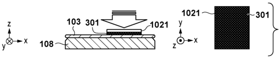
도 2는, 몰드 보유지지 유닛(101) 및 몰드 보유지지 유닛(101)의 주변부의 구성을 개략적으로 도시하는 단면도이다. 몰드 보유지지 유닛(101)은, 예를 들어 흡착부(110)를 포함하고, 흡착부(110)를 사용하여 몰드(102)를 흡착함으로써 몰드(102)를 보유지지한다. 몰드(102)는 메사 형상 패턴부(메사부)(1021)를 포함한다. 패턴부(1021)(의 패턴면)에는, 기판 상에 형성해야 할 패턴이 형성된다.2 is a cross-sectional view schematically showing the structure of the
몰드 보유지지 유닛(101)은, 예를 들어 경화 유닛(105)으로부터 공급되는, 기판 상의 임프린트재를 경화시키기 위한 에너지를 투과하는 구조를 가지며, 더 구체적으로는, 중공 구조를 갖는다. 몰드 보유지지 유닛(101)은, 몰드(102)의 이면(패턴면의 반대측의 면)의 측에 압력실(캐비티)(133)을 형성하는 시일 부재(예를 들어, 시트 글래스)(112)와, 압력실(133)의 압력을 제어하기 위한 채널(111)과, 압력 제어 유닛(181)을 포함한다.The
압력 제어 유닛(181)은 채널(111)을 통해서 압력실(133)에 연결된다. 압력 제어 유닛(181)은, 예를 들어 압력실(133)의 압력이 외부 공간의 압력보다 높아지도록, 압력실(133)의 압력을 제어한다. 따라서, 몰드(102)는, 몰드(102)의 패턴부(1021)(중앙부)가 기판(103)(하방측)을 향해서 볼록 형상을 갖도록 변형될 수 있다. 압력 제어 유닛(181) 및 채널(111)은, 몰드(102)의 변형을 제어(조정)하는 몰드 변형 기구(180)를 형성한다.The
도 3은 기판 척(108)의 구성을 개략적으로 도시하는 도면이다. 기판 척(108)은, 제어 유닛(190)의 제어 하에서, 기판(103)에 대한 흡착 압력(기판 척(108)이 기판(103)을 보유지지하는 보유지지력)을 제어(조정)하는 압력 제어 기구(300)를 포함한다. 압력 제어 기구(300)는 기판(103)의 이면 측의 압력 분포를 제어한다.3 is a diagram schematically showing the configuration of the
압력 제어 기구(300)는, 기판 척(108)의 표면에 제공된 복수의 오목부(121, 122, 123, 124 및 125)와, 복수의 오목부(121 내지 125)의 압력을 개별적으로 제어할 수 있는 압력 제어 유닛(150)을 포함한다. 복수의 오목부(121 내지 125)는, 기판(103)에 대한 보유지지력을 독립적으로 제어할 수 있는 복수의 보유지지 영역을 형성한다. 예를 들어, 압력 제어 유닛(150)이 -40kPa의 부압을 오목부(122, 123, 124)에 공급하고, -5kPa의 부압을 오목부(121)에 공급하는 경우를 생각한다. 이 경우, 기판(103)의 오목부(121)에 대응하는 영역(부분)을 기판 척(108)과 접촉시키지 않고 기판(103)을 보유지지할 수 있다. 오목부(121 내지 125)의 수는 5개로 한정되는 것이 아니라, 요구되는 사양에 따라서 임의의 수로 변경될 수 있다는 것에 유의한다. 압력 제어 유닛(150)이 오목부(121 내지 125)에 개별적으로 공급할 수 있는 압력의 범위 및 값은 요구되는 사양에 따라서 결정된다. 오목부(121 내지 125)의 형상은, 도 3에 도시되는 바와 같이, 동심원적으로 배치된 원형 형상 또는 링 형상이어도 되거나, 다른 형상이어도 된다. 기판 척(108)은, 기판(103)에 대항하는 면 내에서의 에지에 테이퍼부(TP)를 포함해도 된다. 기판(103)의 이면 측의 압력, 즉, 기판 척(108)과 기판(103)에 의해 둘러싸인 공간의 압력에 관해서는, 이러한 공간의 압력을 계측하는 센서가 제공되고, 센서에 의해 취득된 계측값에 의해 압력을 제어해도 된다.The
도 4는 몰드(102)의 구성을 개략적으로 도시하는 도면이다. 몰드(102)는, 박판 유사 가동부(다이어프램)(1022)와, 가동부(1022)로부터 돌출되도록 제공된 패턴부(1021)와, 가동부(1022)를 지지하는 지지부(1024)를 포함한다. 가동부(1022)의 이면측(패턴부(1021)가 배치된 측의 반대측)에는, 지지부(1024)에 의해 둘러싸인 중공부(1025)가 제공된다. 중공부(1025)는 압력실(133)의 일부를 형성한다.4 is a diagram schematically showing the configuration of the
가동부(1022)는 예를 들어 약 1 mm의 두께를 갖는다. 패턴부(1021)는, 예를 들어 약 30 μm의 두께를 갖는다. 패턴부(1021)의 표면(패턴면)에는, 볼록 패턴(204) 및 오목 패턴(203)으로 형성되는 패턴이 형성된다. 볼록 패턴(204)의 표면과 오목 패턴(203)의 표면 사이의 단차, 즉 볼록 패턴(204)의 높이는, 예를 들어 몇십 nm 내지 몇백 nm의 범위이다. 패턴부(1021)에는, 1개 또는 복수의 마크(206)가 제공된다.The
도 5a 및 도 5b는, 도 4에 도시하는 몰드(102)를 사용해서 기판 상의 임프린트재에 패턴을 형성하는 임프린트 처리를 행할 때에, 도 3에 도시하는 기판 척(108)의 오목부(121 내지 125)와 몰드(102)의 패턴부(1021) 사이의 위치 관계를 도시하는 도면이다. 도 5a 및 도 5b를 참조하면, 기판(103)의 샷 영역(902)은 임프린트 처리를 행하는 대상 영역에 대응한다. 샷 영역(902)에는 몰드(102)의 패턴부(1021)의 전체면이 맞춰지기 때문에, 이러한 샷 영역을 몰드 전체면 샷 영역이라 칭한다. 이 경우, 오목부(122, 123, 124)는 샷 바로 아래 영역(제1 보유지지 영역)으로서 각각 설정되고, 오목부(121 및 125)는 샷 주변 영역(제2 보유지지 영역)으로서 각각 설정된다.5A and 5B show
도 6a, 도 6b, 도 6c, 도 6d, 도 6e, 도 6f, 도 6g, 도 7의 (A) 및 (B)를 참조하면, 임프린트 장치(100)에서의 몰드 전체면 샷 영역에 대한 임프린트 처리를 설명한다. 임프린트 처리는 임프린트 장치(100)의 각 유닛을 통괄적으로 제어하는 제어 유닛(190)에 의해 행해진다.Referring to FIGS. 6A, 6B, 6C, 6D, 6E, 6F, 6G, and 7 (A) and (B), the
도 6a 내지 도 6g는 임프린트 처리 동안의 기판(103)과 몰드(102) 사이의 상태를 나타낸다. 간략화를 위해, 도 6a 내지 도 6g에서는 몰드(102)의 패턴부(1021) 만을 나타낸다. 도 7의 (A)는 몰드(102)를 통해서 기판 상의 임프린트재(301)에 부여되는 가압력의 프로파일을 나타낸다. 몰드(102)에 의해 임프린트재(301)를 가압하는 힘을 부의 가압력으로서 취한다. 도 7의 (A)에서는, 종축은 가압력을 나타내고, 횡축은 시간을 나타낸다. 도 7의 (B)는, 기판(103)에 대한 기판 척(108)의 흡착 압력의 프로파일을 나타내고, 기판(103)이 기판 척(108)에 흡착되는 압력을 부의 흡착 압력으로서 취한다. 도 7의 (B)에서는, 종축은 흡착 압력을 나타내고, 횡축은 시간을 나타내고 있다. 도 7의 (B)에 나타내는 흡착 압력은, 기판(103)에 대한 기판 척(108)의 샷 바로 아래 영역의 흡착 압력을 나타내고, 이하 흡착 압력에 관한 설명은 기판 척(108)의 샷 바로 아래 영역에 대한 것이다. 또한, 도 7의 (A) 및 도 7의 (B)에 나타내는 타이밍(시각)(Tb, Tc, Td, Te, Tf 및 Tg)은, 각각 도 6b, 도 6c, 도 6d, 도 6e, 도 6f 및 도 6g에 나타내는 상태에 대응한다.6A to 6G show a state between the
먼저, 제어 유닛(190)은, 도 6a에 도시하는 바와 같이, 가스 공급 유닛(170)으로부터 몰드(102)와 기판(103) 사이의 공간에 퍼지 가스가 공급된 상태에서, 몰드(102)의 강하를 개시하도록 몰드 구동 유닛(131)을 제어한다. 이에 의해, 공급 유닛(106)으로부터 기판(103)의 샷 영역에 공급된 임프린트재(301)에 몰드(102)가 근접한다. 이때, 제어 유닛(190)은, 기판 척(108)이 기판(103)을 제1 흡착 압력(제1 보유지지력)에서 유지하도록, 압력 제어 기구(300)를 제어한다. 이와 같이, 제어 유닛(190)은, 기판 척(108)에 의해 기판(103)을 제1 흡착 압력에서 보유지지하면서 기판 상의 임프린트재(301)에 몰드(102)를 가압하는 처리(가압 처리)를 개시한다.First, as shown in FIG. 6A , the
제어 유닛(190)은, 몰드(102)가 강하하기 전, 즉 가압 처리를 개시하기 전에, 또는 가압 처리와 병행하여, 몰드(102)가 기판(103)을 향해서 볼록 형상을 갖도록, 압력 제어 유닛(181)을 통해서 압력실(133)의 압력을 제어해도 된다는 것에 유의한다. 일반적으로, 압력 제어 유닛(181)을 통해서 몰드(102)를 목표 볼록 형상으로 변형시키기 위해서는 약 몇백 msec가 걸린다. 그러므로, 공급 유닛(106)에 의한 기판(103)에의 임프린트재(301)의 공급과 병행하여, 압력 제어 유닛(181)에 의한 압력실(133)의 압력의 제어를 개시해도 된다.The
이어서, 제어 유닛(190)은, 도 6b에 도시하는 바와 같이, 기판 상의 임프린트재(301)에 몰드(102)의 패턴부(1021)의 일부를 접촉시킨다(가압한다). 이때, 기판(103)과 몰드(102)의 패턴부(1021) 사이에 가스가 들어가는 것이 방지되도록, 패턴부(1021)의 중심부로부터 시작해서 몰드(102)의 패턴부(1021)를 기판 상의 임프린트재(301)에 접촉시키는 것이 바람직하다. 몰드(102)와 기판(103)이 서로 접근하는 동작은 예를 들어 제1 동작과 제1 동작 후의 제2 동작을 포함한다. 제1 동작에서는, 몰드(102)와 기판(103)을 제1 속도에서 서로 근접시킨다. 제2 동작에서는, 몰드(102)와 기판(103)을 제1 속도보다 늦은 제2 속도에서 서로 근접시켜, 몰드(102)와 기판 상의 임프린트재(301)를 서로 접촉시킨다. 이에 의해, 몰드(102)(의 패턴부(1021))와 기판(103) 사이의 충돌을 방지할 수 있다. 도 6b에 나타내는 상태에서, 몰드(102)를 통해서 기판 상의 임프린트재(301)에 부여되는 가압력 및 기판(103)에 대한 기판 척(108)의 흡착 압력은 각각 도 7의 (A) 및 도 7의 (B)에 나타내는 타이밍(Tb)의 것에 대응한다.Then, as shown in FIG. 6B, the
이어서, 제어 유닛(190)은, 도 6c에 도시하는 바와 같이, 기판 상의 임프린트재(301)가 몰드(102)의 패턴부(1021)의 단부까지 확산되도록 몰드 구동 유닛(131)을 제어한다. 이 기간은, 도 7의 (A)에 도시하는 바와 같이, 몰드(102)를 통해서 기판 상의 임프린트재(301)에 부여하는 가압력이 최대가 되는 타이밍(Tc)까지의 기간, 즉 가압력이 증가되는 제1 기간이다. 기판(103)에 대한 기판 척(108)의 흡착 압력은, 도 7의 (B)에 도시하는 바와 같이, 타이밍(Tc)까지 제1 흡착 압력을 유지한다. 제1 흡착 압력은, 본 실시형태에서는, 기판 상의 임프린트재(301)에 몰드(102)를 접촉시키고 나서 임프린트재(301)로부터 몰드(102)를 분리할 때까지의 사이의 기간에서의 최소 흡착 압력이다. 이 상태에서는, 기판 척(108)과 기판(103)을 서로 밀착시켜서 몰드 구동 유닛(131)의 힘을 방출시키지 않는 것이 목적이기 때문에, 기판 척(108)은 기판(103)에 대해 낮은 흡착 압력을 갖는 것이 바람직하다.Next, the
이어서, 제어 유닛(190)은, 도 6d에 도시하는 바와 같이, 기판 상의 임프린트재(301)가 몰드(102)의 패턴부(1021)의 전체면에 걸쳐 확산되도록, 몰드 구동 유닛(131)을 제어한다. 이 기간은, 도 7의 (A)에 도시하는 바와 같이, 몰드(102)를 통해서 기판 상의 임프린트재(301)에 부여하는 가압력을 감소시키는 제2 기간(타이밍 Tc로부터 타이밍 Te까지의 기간) 중 타이밍 Tc로부터 타이밍 Td까지의 기간이다. 기판(103)에 대한 기판 척(108)의 흡착 압력은, 도 7의 (B)에 도시하는 바와 같이, 제1 기간으로부터 제2 기간으로 이행하는 타이밍(타이밍 Tc)에서, 제1 흡착 압력보다 낮은 제2 흡착 압력으로 설정된다(제1 보유지지력보다 작은 제2 보유지지력으로 전환된다). 제2 흡착 압력(제2 보유지지력)은, 본 실시형태에서는, 기판 상의 임프린트재(301)에 몰드(102)를 접촉시키고 나서 임프린트재(301)로부터 몰드(102)를 분리할 때까지의 기간에서의 최대 흡착 압력이다. 이와 같이, 기판 척(108)과 기판(103) 사이의 밀착을 느슨하게 함으로써, 기판 상의 임프린트재(301)에 전사되는 기판 척(108)의 거칠기를 해방(release)한다. 기판 척(108)과 기판(103) 사이의 밀착을 해방하기 위해서, 제2 흡착 압력을 0으로 설정해도 된다.Next, the
이어서, 제어 유닛(190)은, 도 6e에 도시하는 바와 같이, 기판 상의 임프린트재(301)가 몰드(102)의 패턴부(1021)의 전체면에 걸쳐 확산된 상태를 유지하도록, 몰드 구동 유닛(131)을 제어한다. 이에 의해, 기판 상의 임프린트재(301)가 몰드(102)의 패턴부(1021)(오목 패턴(203))에 충전된다. 이 기간은, 도 7의 (A)에 도시하는 바와 같이, 몰드(102)를 통해서 기판 상의 임프린트재(301)에 부여하는 가압력을 감소시키는 제2 기간 중, 타이밍 Td로부터 타이밍 Te까지의 기간이다. 기판(103)에 대한 기판 척(108)의 흡착 압력은, 도 7의 (B)에 도시하는 바와 같이, 타이밍 Te까지 제2 흡착 압력을 유지한다. 그리고, 제2 기간이 종료하는 타이밍(타이밍 Te)에서, 제2 흡착 압력보다 높은 제3 흡착 압력이 설정된다(제2 보유지지력보다 큰 제3 보유지지력으로의 전환이 행해진다). 제3 흡착 압력(제3 보유지지력)은, 본 실시형태에서는, 제1 흡착 압력보다 낮은 흡착 압력이지만(제1 보유지지력보다 작다), 제1 흡착 압력과 동등해도 된다.Then, as shown in FIG. 6E, the
이어서, 제어 유닛(190)은, 도 6f에 도시하는 바와 같이, 기판 상의 임프린트재(301)를 경화시키는 에너지가 기판 상의 임프린트재(301)에 공급되도록, 경화 유닛(105)을 제어한다. 이에 의해, 기판 상의 임프린트재(301)가 경화되고, 몰드(102)의 패턴부(1021)에 형성되어 있는 패턴이 임프린트재(301)에 전사된다. 도 6f에 나타내는 상태에서, 몰드(102)를 통해서 기판 상의 임프린트재(301)에 부여되는 가압력 및 기판(103)에 대한 기판 척(108)의 흡착 압력은 각각 도 7의 (A) 및 도 7의 (B)에 나타내는 타이밍 Tf에 대응한다.Then, as shown in FIG. 6F, the
이어서, 제어 유닛(190)은, 도 6g에 도시하는 바와 같이, 기판 상의 경화된 임프린트재(301)로부터 몰드(102)가 분리되도록, 몰드 구동 유닛(131)을 제어한다. 도 6g에 나타내는 상태에서, 몰드(102)를 개재해서 기판 상의 임프린트재(301)에 부여되는 가압력 및 기판(103)에 대한 기판 척(108)의 흡착 압력은 각각 도 7의 (A) 및 도 7의 (B)에 나타내는 타이밍 Tg의 것에 대응한다.Next, the
상술한 바와 같이, 본 실시형태에서는, 가압 처리를 개시한 후, 예를 들어 몰드(102)를 통해서 기판 상의 임프린트재(301)에 가압력이 부여되는 기간에, 기판(103)에 대한 기판 척(108)의 흡착 압력을 제1 흡착 압력으로부터 제2 흡착 압력으로 전환한다. 기판 척(108)이 기판(103)을 제2 흡착 압력에서 보유지지하는 상태를 기판 상의 임프린트재(301)의 몰드(102)에의 충전이 완료될 때까지 유지한다. 이에 의해, 몰드(102)로부터 임프린트재(301)로의 가압력이 충분히 전해지며, 기판 척(108)의 거칠기가 기판 상에 형성되는 패턴에 전사되는 것이 억제되기 때문에, 수율을 향상시킬 수 있다.As described above, in the present embodiment, after starting the pressing process, for example, during a period in which pressing force is applied to the
또한, 본 실시형태에서는, 기판 상의 임프린트재(301)의 몰드(102)로의 충전이 완료된 후, 임프린트재(301)를 경화시키기 전에, 기판(103)에 대한 기판 척(108)의 흡착 압력을 제2 흡착 압력으로부터 제3 흡착 압력으로 전환한다. 이에 의해, 기판 상에 형성되는 패턴의 전사 정밀도를 유지할 수 있으며, 기판 상의 경화된 임프린트재(301)로부터 몰드(102)를 분리하는 때에 디처킹(dechucking)의 발생을 방지할 수 있다. 기판(103)에 대한 기판 척(108)의 흡착 압력을 제2 흡착 압력으로부터 제3 흡착 압력으로 전환하는 타이밍은, 임프린트재(301)를 경화시킨 후, 임프린트재(301)로부터 몰드(102)를 분리하기 전으로 설정되어도 된다는 것에 유의한다.Further, in this embodiment, after the filling of the
기판 척(108)의 샷 바로 아래 영역을 제외하는 샷 주변 영역에 관해서는, 기판(103)에 대한 흡착 압력을 전환할 필요는 없다. 기판 척(108)의 샷 주변 영역에 대해서는, 가압 처리를 개시하고 나서 임프린트재(301)의 몰드(102)에의 충전이 완료할 때까지, 또는 더 구체적으로는 임프린트재(301)로부터 몰드(102)를 분리할 때까지의 기간 동안 기판(103)을 제1 흡착 압력으로 보유지지하는 상태를 유지하면 충분하다. 즉, 임프린트 처리 동안, 기판 척(108)의 샷 바로 아래 영역 이외의 영역에서는 기판(103)의 보유지지를 유지한다. 이에 의해, 기판 척(108)에서의 기판(103)의 위치 어긋남을 저감할 수 있다.As for the area around the shot, except for the area immediately below the shot of the
본 실시형태는, 몰드(102)를 통해서 기판 상의 임프린트재(301)에 부여되는 가압력의 프로파일(도 7의 (A))에 기초하여, 기판(103)에 대한 기판 척(108)의 흡착 압력을 제1 흡착 압력으로부터 제2 흡착 압력으로 전환하는 경우를 예시했다. 그러나, 관찰 유닛(114)에 의해 취득되는 기판 상의 임프린트재(301)의 몰드(102)에의 충전 상태에 기초하여, 기판(103)에 대한 기판 척(108)의 흡착 압력을 제1 흡착 압력으로부터 제2 흡착 압력으로 전환해도 된다. 더 구체적으로는, 관찰 유닛(114)에 의해 취득된 충전 상태가 기판 상의 임프린트재(301)가 몰드(102)의 전체면에 걸쳐 충전된 상태일 때에, 기판(103)에 대한 기판 척(108)의 흡착 압력을 제1 흡착 압력으로부터 제2 흡착 압력으로 전환한다.In this embodiment, based on the profile of the pressing force applied to the
또한, 임프린트 장치(100)에서는, 몰드 전체면 샷 영역뿐만 아니라, 도 8a 및 도 8b에 도시하는 바와 같이 부분 샷 영역에 대하여도 임프린트 처리가 행해진다. 여기서, 부분 샷 영역은, 몰드(102)의 패턴부(1021)에 형성된 패턴의 일부가 기판 상의 임프린트재에 전사되는 샷 영역이며, 기판(103)의 외주(에지)를 포함하는 샷 영역이다.Further, in the
도 8a 및 도 8b는, 도 4에 도시하는 몰드(102)를 사용해서 기판(103)의 부분 샷 영역에 임프린트 처리를 행할 때에, 도 3에 도시하는 기판 척(108)의 오목부(121 내지 125)와 몰드(102)의 패턴부(1021) 사이의 위치 관계를 도시하는 도면이다. 도 8a 및 도 8b를 참조하면, 기판(103)의 샷 영역(903)에는 몰드(102)의 패턴부(1021)의 전체면이 맞지 않기 때문에, 이러한 샷 영역을 부분 샷 영역이라고 칭한다. 이 경우, 오목부(121 및 122) 각각을 샷 바로 아래 영역(제1 보유지지 영역)으로서 설정하고, 오목부(123, 124 및 125) 각각을 샷 주변 영역(제2 보유지지 영역)으로서 설정한다. 기판(103)의 부분 샷 영역에 임프린트 처리를 행하는 경우, 몰드 전체면 샷 영역에 임프린트 처리를 행하는 경우와 마찬가지로, 기판(103)에 대한 기판 척(108)의 흡착 압력을 제어하면 된다. 즉, 부분 샷 영역과 몰드 전체면 샷 영역 사이에서, 기판(103)에 대한 기판 척(108)의 흡착 압력의 제어에 차이는 없다.8A and 8B show the
도 9를 참조하여, 임프린트 장치(100)의 동작(기판(103)의 각 샷 영역에 대한 임프린트 처리)을 설명한다. 단계 S801에서는, 기판 척(108)에 기판(103)을 로드한다. 단계 S802에서는, 기판(103)의 복수의 샷 영역으로부터, 임프린트 처리를 행하는 대상 영역인 대상 샷 영역을 선택한다.Referring to FIG. 9 , the operation of the imprint apparatus 100 (imprint processing for each shot region of the substrate 103) will be described. In step S801 , a
단계 S803에서는, 단계 S802에서 선택한 대상 샷 영역에 대응하는, 몰드(102)를 통해서 기판 상의 임프린트재에 부여되는 가압력의 프로파일(도 7의 (A))을 취득한다. 가압력의 프로파일은, 예를 들어 레시피로부터 취득되는 대상 샷 영역에 대한 몰드 구동 유닛(131)의 구동 프로파일 및 임프린트재의 특성 등의 정보를 사용한 시뮬레이션에 의해 구해질 수 있다. 단계 S804에서는, 단계 S803에서 취득한 가압력의 프로파일에 기초하여, 기판(103)에 대한 기판 척(108)의 흡착 압력의 프로파일(도 7의 (B))을 생성한다.In step S803, the profile of the pressing force applied to the imprint material on the substrate via the mold 102 (FIG. 7(A)) corresponding to the target shot region selected in step S802 is acquired. The profile of the pressing force can be obtained by simulation using, for example, information such as the driving profile of the
단계 S805에서는, 단계 S802에서 선택한 대상 샷 영역에 대하여 임프린트 처리를 행한다. 임프린트 처리에서는, 단계 S804에서 생성된 프로파일에 따라서 기판(103)에 대한 기판 척(108)의 흡착 압력을 제어한다.In step S805, an imprint process is performed on the target shot region selected in step S802. In the imprint process, the adsorption pressure of the
단계 S806에서는, 대상 샷 영역으로서 선택되지 않은 샷 영역이 있는지를 판정한다. 대상 샷 영역으로서 선택되지 않은 샷 영역이 있을 경우에는, 새로운 대상 샷 영역을 선택하기 위해서 처리는 단계 S802로 복귀한다. 한편, 대상 샷 영역으로서 선택되지 않은 샷 영역이 없을 경우에는, 처리는 단계 S807로 이행한다. 단계 S807에서는, 기판 척(108)으로부터 기판(103)을 언로드한다.In step S806, it is determined whether there is a shot area not selected as a target shot area. If there is a shot region not selected as the target shot region, the process returns to step S802 to select a new target shot region. On the other hand, if there is no unselected shot area as the target shot area, the process proceeds to step S807. In step S807, the
임프린트 장치(100)를 사용해서 형성한 경화물의 패턴은, 각종 물품의 적어도 일부에 영구적으로 혹은 각종 물품을 제조할 때에 일시적으로 사용된다. 물품은 전기 회로 소자, 광학 소자, MEMS, 기록 소자, 센서, 몰드 등이다. 전기 회로 소자의 예는, DRAM, SRAM, 플래시 메모리, 및 MRAM 등의 휘발성 및 불휘발성 반도체 메모리와, LSI, CCD, 이미지 센서, 및 FPGA 등의 반도체 소자이다. 몰드의 예는 임프린트용 몰드이다.The pattern of the cured product formed using the
경화물의 패턴은, 상술한 물품의 적어도 일부의 구성 부재로서 그대로 사용되거나 혹은 레지스트 마스크로서 일시적으로 사용된다. 기판 가공 단계에서 에칭 또는 이온 주입 등이 행해진 후, 레지스트 마스크는 제거된다.The pattern of the cured product is used as it is as a constituent member of at least a part of the above-described article or temporarily used as a resist mask. After etching or ion implantation or the like is performed in the substrate processing step, the resist mask is removed.
이어서, 물품의 상세한 제조 방법에 대해서 설명한다. 도 10a에 도시하는 바와 같이, 절연체 등의 피가공재가 표면에 형성된 실리콘 웨이퍼 등의 기판(103)을 준비한다. 계속해서, 잉크젯법 등에 의해 피가공재의 표면에 임프린트재를 부여한다. 여기에서는, 복수의 액적으로서 임프린트재가 기판 상에 부여된 상태를 나타내고 있다.Next, the detailed manufacturing method of an article is demonstrated. As shown in Fig. 10A, a
도 10b에 도시하는 바와 같이, 임프린트용 몰드(102)의, 불균일 패턴을 갖는 측을 기판 상의 임프린트재를 향해 대향시킨다. 도 10c에 도시하는 바와 같이, 임프린트재가 부여된 기판(103)을 몰드(102)와 접촉시키고, 압력을 가한다. 몰드(102)와 피가공재 사이의 간극에 임프린트재가 충전된다. 이 상태에서, 경화용 에너지를 몰드(102)를 통해서 임프린트재에 조사하면, 임프린트재가 경화한다.As shown in Fig. 10B, the side having the non-uniform pattern of the
도 10d에 도시하는 바와 같이, 임프린트재를 경화시킨 후, 몰드(102)를 기판(103)으로부터 분리한다. 그후, 임프린트재의 경화물의 패턴이 기판 상에 형성된다. 이 경화물의 패턴에서, 몰드(102)의 오목 패턴이 경화물의 볼록부에 대응하고, 몰드(102)의 볼록 패턴이 경화물의 오목부에 대응한다. 즉, 몰드(102)의 불균일 패턴이 임프린트재에 전사된다.As shown in FIG. 10D, after the imprint material is cured, the
도 10e에 도시하는 바와 같이, 경화물의 패턴을 에칭 저항 마스크로서 사용하여 에칭을 행하면, 피가공재의 표면 중, 경화물이 존재하지 않거나 얇게 잔존하는 부분이 제거되어 홈을 형성한다. 도 10f에 도시하는 바와 같이, 경화물의 패턴을 제거하면, 피가공재의 표면에 홈이 형성된 물품을 얻을 수 있다. 여기서, 경화물의 패턴이 제거된다. 그러나, 경화물의 패턴을 가공 또는 제거하는 대신에, 이것을 예를 들어 반도체 소자 등에 포함되는 층간 절연막, 즉 물품의 구성 부재로서 이용해도 된다.As shown in FIG. 10E, when etching is performed using the pattern of the cured material as an etching resistance mask, portions of the surface of the workpiece where no cured material or remaining thin are removed to form grooves. As shown in FIG. 10F, if the pattern of the cured product is removed, an article having grooves formed on the surface of the workpiece can be obtained. Here, the pattern of the cured product is removed. However, instead of processing or removing the pattern of the cured product, it may be used, for example, as an interlayer insulating film included in a semiconductor element or the like, that is, as a constituent member of an article.
본 실시형태는, 몰드(102)로서, 불균일 패턴을 설치한 회로 패턴을 전사하기 위한 몰드를 예시하였다는 것에 유의한다. 그러나, 몰드(102)는, 불균일 패턴이 없는 평탄부를 갖는 평탄한 템플릿이어도 된다. 평탄한 템플릿(부재)은, 평탄부를 사용하여 기판 상의 조성물을 평탄해지도록 성형하는 평탄화 처리(성형 처리)를 행하는 평탄화 장치(성형 장치)에 사용된다. 평탄화 처리는, 기판 상에 공급된 경화성 조성물에 평탄한 템플릿의 평탄부를 접촉시킨 상태에서, 광의 조사 혹은 가열에 의해 경화성 조성물을 경화시키는 공정을 포함한다. 이와 같이, 본 실시형태는, 평탄한 템플릿을 사용해서 기판 상의 조성물을 성형하는 성형 장치에 적용할 수 있다.Note that in this embodiment, as the
기판 상의 하부 패턴은, 전 단계에서 형성된 패턴에 기인하는 오목/볼록 프로파일을 갖는다. 더 구체적으로는, 기판(프로세스 웨이퍼)은 근년의 메모리 소자의 다층 구조화에 수반하여 약 100 nm의 단차를 가져도 된다. 기판의 전체면의 완만한 파상(undulation)에 기인하는 단차는, 포토리소그래피 공정에서 사용되는 노광 장치(스캐너)의 포커스 추종 기능에 의해 보정될 수 있다. 그러나, 작은 피치를 가지며 노광 장치의 노광 슬릿 면적 내에 들어오는 미세한 오목/볼록부는 그대로 노광 장치의 DOF(Depth Of Focus)를 소비한다. 기판의 하부 패턴을 평탄화하는 종래 기술로서, SOC(Spin On Carbon) 또는 CMP(Chemical Mechanical Polishing) 등의 평탄화층을 형성하는 기술이 사용된다. 그러나, 종래 기술에서는, 도 11a에 도시하는 바와 같이, 고립 패턴 영역(A)과 반복적 덴스(Dense)(선 및 공간 패턴의 밀집) 패턴 영역(B) 사이의 경계 부분에서 40% 내지 70%의 불균일성 억제율만이 얻어질 수 있고, 그래서 충분한 평탄화 성능이 얻어질 수 없다. 또한, 다층 형성에 의한 하부 패턴의 오목/볼록 차가 증가하는 경향이 있다.The lower pattern on the substrate has a concave/convex profile due to the pattern formed in the previous step. More specifically, the substrate (process wafer) may have a level difference of about 100 nm in accordance with the multi-layer structure of memory devices in recent years. A level difference due to gentle undulation of the entire surface of the substrate can be corrected by a focus follow-up function of an exposure device (scanner) used in a photolithography process. However, fine concave/convex portions having a small pitch and entering the exposure slit area of the exposure apparatus consume the Depth Of Focus (DOF) of the exposure apparatus as they are. As a conventional technique for planarizing the lower pattern of the substrate, a technique for forming a planarization layer such as SOC (Spin On Carbon) or CMP (Chemical Mechanical Polishing) is used. However, in the prior art, as shown in FIG. 11A, 40% to 70% of the boundary portion between the isolated pattern area A and the repetitive dense (dense line and space pattern) pattern area B Only the non-uniformity suppression rate can be obtained, and therefore sufficient planarization performance cannot be obtained. In addition, the concave/convex difference of the lower pattern due to multilayer formation tends to increase.
이 문제에 대한 해결책으로서, 미국 특허 제9415418호는, 평탄화층의 역할을 하는 레지스트를 잉크젯 디스펜서에 의해 도포하고 평탄한 템플릿에 의해 압인함으로써 연속막을 형성하는 기술을 제안한다. 또한, 미국 특허 제8394282호는, 기판 측의 토포그래피 계측 결과를 잉크젯 디스펜서에 의해 레지스트의 도포가 지시되는 각 위치에 대한 농도 정보에 반영하는 기술을 제안하고 있다. 임프린트 장치(100)는, 특히, 미리 도포된 미경화 레지스트(미경화 재료)에 대하여 몰드(102) 대신 평탄한 템플릿을 가압하여 기판의 표면을 국소적으로 평탄화하는 평탄가공(평탄화) 장치로서 적용될 수 있다.As a solution to this problem, US Patent No. 9415418 proposes a technique of forming a continuous film by applying a resist serving as a flattening layer by means of an inkjet dispenser and stamping it by means of a flattening template. In addition, US Patent No. 8394282 proposes a technique of reflecting the topography measurement result on the substrate side to density information for each position where application of a resist is directed by an inkjet dispenser. The
도 11a는 평탄가공을 행하기 전의 기판을 나타내고 있다. 고립 패턴 영역(A)에서는 볼록 패턴부의 면적이 작다. 반복 덴스 패턴 영역(B)에서, 볼록 패턴부가 차지하는 면적과 오목 패턴부가 차지하는 면적은 1:1이다. 고립 패턴 영역(A)과 반복 덴스 패턴 영역(B)의 평균 높이는 볼록 패턴부가 차지하는 비율에 따라 상이한 값을 갖는다.Fig. 11A shows the substrate before flattening. In the isolated pattern region (A), the area of the convex pattern portion is small. In the repeated dense pattern region B, the area occupied by the convex pattern portion and the area occupied by the concave pattern portion are 1:1. The average heights of the isolated pattern area (A) and the repeated dense pattern area (B) have different values depending on the occupied ratio of the convex pattern portion.
도 11b는 평탄화층을 형성하는 레지스트를 기판에 도포한 상태를 나타내고 있다. 도 11b는, 미국 특허 제9415418호에 제안된 기술에 기초하여 잉크젯 디스펜서에 의해 레지스트를 도포한 상태를 나타낸다. 그러나, 스핀 코터를 레지스트를 도포하기 위해 사용해도 된다. 즉, 미리 도포된 미경화 레지스트에 대하여 평탄한 템플릿을 가압해서 평탄화하는 단계를 포함하고 있는 한, 임프린트 장치(100)가 적용될 수 있다.Fig. 11B shows a state in which a resist forming a planarization layer is applied to the substrate. Fig. 11B shows a state in which a resist is applied by an inkjet dispenser based on the technique proposed in US Patent No. 9415418. However, a spin coater may be used to apply the resist. That is, the
도 11c에 도시하는 바와 같이, 평탄한 템플릿은, 자외선을 투과하는 유리 또는 석영으로 구성되고, 광원으로부터의 자외선의 조사에 의해 레지스트가 경화한다. 평탄한 템플릿은, 기판 전체의 완만한 불균일성에 대해서는 기판 표면의 프로파일에 합치한다. 레지스트가 경화된 후, 도 11d에 도시하는 바와 같이, 레지스트로부터 평탄한 템플릿을 분리한다.As shown in FIG. 11C, the flat template is made of glass or quartz that transmits ultraviolet rays, and the resist is cured by irradiation of ultraviolet rays from a light source. The flat template conforms to the profile of the substrate surface for minor irregularities across the substrate. After the resist is cured, the flat template is separated from the resist as shown in Fig. 11D.
볼 발명은 예시적인 실시형태를 참조하여 설명되었지만, 본 발명은 개시된 예시적인 실시형태로 한정되지 않음을 이해해야 한다. 이하의 청구항의 범위는 이러한 모든 변형과 동등한 구조 및 기능을 포함하도록 최광의의 해석이 부여된다.Although the present invention has been described with reference to exemplary embodiments, it should be understood that the present invention is not limited to the disclosed exemplary embodiments. The scope of the following claims is to be accorded the broadest interpretation so as to encompass all such modifications and equivalent structures and functions.
Claims (17)
복수의 오목부를 포함하고, 상기 복수의 오목부의 압력을 부압(negative pressure)으로 되게 함으로써 상기 기판을 보유지지하도록 구성된 보유지지 유닛; 및
상기 성형 처리를 제어하도록 구성된 제어 유닛을 포함하고,
상기 제어 유닛은,
상기 기판이 상기 보유지지 유닛에 의해 제1 보유지지력으로 보유지지되는 상태에서 상기 기판의 대상 영역 상의 상기 조성물에 대해 상기 몰드를 가압하는 처리를 개시하고,
상기 몰드를 가압하는 처리가 개시된 후에, 상기 복수의 오목부 중 상기 대상 영역의 아래에 있는 제1 오목부의 압력을 증가시켜 상기 제1 오목부의 압력을 부압으로 또는 0으로 되게 함으로써, 상기 보유지지 유닛이 상기 제1 보유지지력보다 작은 제2 보유지지력으로 상기 기판을 보유지지하게 하고,
상기 보유지지 유닛이 상기 기판을 상기 제2 보유지지력으로 보유지지하는 상태를 상기 기판 상의 상기 조성물의 상기 몰드에의 충전이 완료될 때까지 유지하는, 성형 장치.A molding device that performs a molding process of molding a composition on a target region of a substrate using a mold,
a holding unit including a plurality of concave portions and configured to hold the substrate by making a pressure of the plurality of concave portions a negative pressure; and
a control unit configured to control the molding process;
The control unit,
Initiating a process of pressing the mold against the composition on a target region of the substrate while the substrate is held with a first holding force by the holding unit;
After the process of pressurizing the mold is started, by increasing the pressure of a first concave portion of the plurality of concave portions below the target region to make the pressure of the first concave portion negative or zero, the holding unit holding the substrate with a second holding force smaller than the first holding force;
and maintaining a state in which the holding unit holds the substrate with the second holding force until filling of the mold with the composition on the substrate is completed.
상기 제어 유닛은, 상기 복수의 제1 오목부의 압력을 증가시켜 상기 복수의 제1 오목부의 압력을 부압으로 또는 0으로 되게 함으로써, 상기 보유지지 유닛이 상기 기판을 상기 제1 보유지지력보다 작은 상기 제2 보유지지력으로 보유지지하게 하는, 성형 장치.The method of claim 1, wherein there are a plurality of first concave portions below the target region,
The control unit increases the pressure of the plurality of first concave portions to make the pressure of the plurality of first concave portions negative or zero, so that the holding unit holds the substrate in the first holding force smaller than the first holding force. A molding device capable of being held by 2 holding forces.
상기 제어 유닛은, 상기 몰드를 가압하는 처리가 상기 제1 기간으로부터 상기 제2 기간으로 이행하는 타이밍에서, 상기 보유지지 유닛이 상기 기판을 보유지지하는 보유지지력을 상기 제1 보유지지력으로부터 상기 제2 보유지지력으로 전환하는, 성형 장치.The method of claim 1, wherein the process of pressing the mold includes a first period in which a pressing force applied to the composition on the substrate through the mold is increased, and a second period in which the pressing force is decreased,
The control unit is configured to change a holding force by which the holding unit holds the substrate from the first holding force to the second holding force at a timing when the process of pressurizing the mold shifts from the first period to the second period. A molding device that converts to holding power.
상기 제어 유닛은, 상기 취득 유닛에 의해 취득되는 상기 충전 상태에 기초하여, 상기 보유지지 유닛이 상기 기판을 보유지지하는 보유지지력을 상기 제1 보유지지력으로부터 상기 제2 보유지지력으로 전환하는, 성형 장치.The method of claim 1, further comprising an acquisition unit configured to acquire a state of filling of the composition on the substrate into the mold,
wherein the control unit switches a holding force by which the holding unit holds the substrate from the first holding force to the second holding force based on the state of charge acquired by the acquiring unit. .
상기 제어 유닛은, 상기 복수의 보유지지 영역 중 상기 대상 영역에 대응하는 영역을 보유지지하는 제1 보유지지 영역에서, 상기 몰드를 가압하는 처리가 개시된 후에 상기 기판이 상기 제2 보유지지력으로 보유지지되게 하고, 상기 기판을 상기 제2 보유지지력으로 보유지지하는 상태를 상기 기판 상의 상기 조성물의 상기 몰드에의 충전이 완료될 때까지 유지하며,
상기 제어 유닛은, 상기 복수의 보유지지 영역 중 상기 제1 보유지지 영역을 제외한 제2 보유지지 영역에서, 상기 몰드를 가압하는 처리의 개시로부터 상기 기판 상의 상기 조성물의 상기 몰드에의 충전이 완료될 때까지의 기간 동안 상기 기판을 상기 제1 보유지지력으로 보유지지하는 상태를 유지하는, 성형 장치.The method of claim 1, wherein the holding unit includes a plurality of holding areas capable of independently controlling a holding force with respect to the substrate,
The control unit is configured to hold the substrate with the second holding force after the process of pressing the mold is started in a first holding area holding an area corresponding to the target area among the plurality of holding areas. and maintaining the state of holding the substrate with the second holding force until filling of the mold with the composition on the substrate is completed,
The control unit controls the filling of the composition on the substrate into the mold from the start of the process of pressurizing the mold in a second holding area excluding the first holding area among the plurality of holding areas. maintaining a state in which the substrate is held by the first holding force for a period of time until
성형 장치를 사용하여 패턴을 기판 상에 형성하는 성형 단계와;
상기 성형 단계에서 상기 패턴이 형성된 상기 기판을 처리하는 단계와;
처리된 상기 기판으로부터 상기 물품을 제조하는 단계를 포함하고,
상기 성형 장치는, 몰드를 사용하여 상기 기판의 대상 영역 상에 조성물을 성형하는 성형 처리를 행하고,
복수의 오목부를 포함하고, 상기 복수의 오목부의 압력을 부압으로 되게 함으로써 상기 기판을 보유지지하도록 구성된 보유지지 유닛과,
상기 성형 처리를 제어하도록 구성된 제어 유닛을 포함하며,
상기 제어 유닛은,
상기 기판이 상기 보유지지 유닛에 의해 제1 보유지지력으로 보유지지되는 상태에서 상기 기판의 대상 영역 상의 상기 조성물에 대해 상기 몰드를 가압하는 처리를 개시하고,
상기 몰드를 가압하는 처리가 개시된 후에, 상기 복수의 오목부 중 상기 대상 영역의 아래에있는 제1 오목부의 압력을 증가시켜 상기 제1 오목부의 압력을 부압으로 또는 0으로 되게 함으로써, 상기 보유지지 유닛이 상기 제1 보유지지력보다 작은 제2 보유지지력으로 상기 기판을 보유지지하게 하고,
상기 보유지지 유닛이 상기 기판을 상기 제2 보유지지력으로 보유지지하는 상태를 상기 기판 상의 상기 조성물의 상기 몰드에의 충전이 완료될 때까지 유지하는, 물품 제조 방법.A method of manufacturing an article,
a forming step of forming a pattern on the substrate using a forming device;
processing the substrate on which the pattern is formed in the forming step;
manufacturing the article from the treated substrate;
The shaping apparatus performs a shaping process of shaping a composition on a target region of the substrate using a mold;
a holding unit including a plurality of concave portions and configured to hold the substrate by making the pressure of the plurality of concave portions negative pressure;
a control unit configured to control the molding process;
The control unit,
Initiating a process of pressing the mold against the composition on a target region of the substrate while the substrate is held with a first holding force by the holding unit;
After the process of pressurizing the mold is started, by increasing the pressure of a first concave portion of the plurality of concave portions below the target region to make the pressure of the first concave portion negative or zero, the holding unit holding the substrate with a second holding force smaller than the first holding force;
and maintaining a state in which the holding unit holds the substrate with the second holding force until filling of the mold with the composition on the substrate is completed.
Applications Claiming Priority (2)
| Application Number | Priority Date | Filing Date | Title |
|---|---|---|---|
| JPJP-P-2018-076246 | 2018-04-11 | ||
| JP2018076246A JP7033994B2 (en) | 2018-04-11 | 2018-04-11 | Molding equipment and manufacturing method of articles |
Publications (2)
| Publication Number | Publication Date |
|---|---|
| KR20190118972A KR20190118972A (en) | 2019-10-21 |
| KR102518784B1 true KR102518784B1 (en) | 2023-04-07 |
Family
ID=68161669
Family Applications (1)
| Application Number | Title | Priority Date | Filing Date |
|---|---|---|---|
| KR1020190041201A KR102518784B1 (en) | 2018-04-11 | 2019-04-09 | Molding apparatus and method of manufacturing article |
Country Status (5)
| Country | Link |
|---|---|
| US (1) | US11372327B2 (en) |
| JP (1) | JP7033994B2 (en) |
| KR (1) | KR102518784B1 (en) |
| CN (1) | CN110361929B (en) |
| TW (1) | TWI736863B (en) |
Families Citing this family (4)
| Publication number | Priority date | Publication date | Assignee | Title |
|---|---|---|---|---|
| JP6762853B2 (en) * | 2016-11-11 | 2020-09-30 | キヤノン株式会社 | Equipment, methods, and article manufacturing methods |
| WO2019188932A1 (en) * | 2018-03-30 | 2019-10-03 | 富士フイルム株式会社 | Mold for manufacturing transdermal absorption sheet, and device and method for manufacturing transdermal absorption sheet having needle-like protrusion |
| JP2022045186A (en) * | 2020-09-08 | 2022-03-18 | キヤノン株式会社 | Molding apparatus and method of manufacturing article |
| WO2022159468A1 (en) * | 2021-01-20 | 2022-07-28 | Applied Materials, Inc. | Anti-slippery stamp landing ring |
Citations (2)
| Publication number | Priority date | Publication date | Assignee | Title |
|---|---|---|---|---|
| JP2010098310A (en) | 2008-10-17 | 2010-04-30 | Asml Netherlands Bv | Imprint lithography apparatus and method |
| JP2017103399A (en) * | 2015-12-03 | 2017-06-08 | キヤノン株式会社 | Imprint apparatus and article manufacturing method |
Family Cites Families (17)
| Publication number | Priority date | Publication date | Assignee | Title |
|---|---|---|---|---|
| CN101573659A (en) | 2005-12-08 | 2009-11-04 | 分子制模股份有限公司 | Method for expelling gas positioned between a substrate and a mold |
| JP4845564B2 (en) | 2006-03-31 | 2011-12-28 | 株式会社東芝 | Pattern transfer method |
| JP5349588B2 (en) | 2008-06-09 | 2013-11-20 | ボード・オブ・リージエンツ,ザ・ユニバーシテイ・オブ・テキサス・システム | Adaptive nanotopography sculpting |
| JP2010067796A (en) * | 2008-09-11 | 2010-03-25 | Canon Inc | Imprint device |
| KR20130073890A (en) * | 2010-04-27 | 2013-07-03 | 몰레큘러 임프린츠 인코퍼레이티드 | Separation control substrate/template for nanoimprint lithography |
| JP5744423B2 (en) | 2010-06-18 | 2015-07-08 | キヤノン株式会社 | Imprint apparatus, imprint method, and device manufacturing method |
| JP6004738B2 (en) | 2011-09-07 | 2016-10-12 | キヤノン株式会社 | Imprint apparatus and article manufacturing method using the same |
| JP6029494B2 (en) | 2012-03-12 | 2016-11-24 | キヤノン株式会社 | Imprint method, imprint apparatus, and article manufacturing method using the same |
| JP6120677B2 (en) | 2013-05-27 | 2017-04-26 | キヤノン株式会社 | Imprint apparatus, imprint method, and article manufacturing method |
| CN105682808B (en) | 2013-08-19 | 2018-03-27 | 德克萨斯大学系统董事会 | With the film of the deposition User Defined profile of nanoscale accuracy programmable |
| JP5745129B2 (en) | 2014-04-02 | 2015-07-08 | キヤノン株式会社 | Imprint apparatus and imprint method |
| JP6333031B2 (en) * | 2014-04-09 | 2018-05-30 | キヤノン株式会社 | Imprint apparatus and article manufacturing method |
| JP2015220299A (en) * | 2014-05-16 | 2015-12-07 | キヤノン株式会社 | Imprint device and method of manufacturing article |
| JP6659104B2 (en) * | 2014-11-11 | 2020-03-04 | キヤノン株式会社 | Imprint method, imprint apparatus, mold, and article manufacturing method |
| JP6437387B2 (en) | 2015-05-25 | 2018-12-12 | 東芝メモリ株式会社 | Substrate flattening method |
| US11104057B2 (en) * | 2015-12-11 | 2021-08-31 | Canon Kabushiki Kaisha | Imprint apparatus and method of imprinting a partial field |
| JP2017139268A (en) | 2016-02-01 | 2017-08-10 | キヤノン株式会社 | Imprint device and method of manufacturing article |
-
2018
- 2018-04-11 JP JP2018076246A patent/JP7033994B2/en active Active
-
2019
- 2019-03-25 TW TW108110232A patent/TWI736863B/en active
- 2019-04-04 US US16/374,821 patent/US11372327B2/en active Active
- 2019-04-09 KR KR1020190041201A patent/KR102518784B1/en active IP Right Grant
- 2019-04-11 CN CN201910286880.6A patent/CN110361929B/en active Active
Patent Citations (2)
| Publication number | Priority date | Publication date | Assignee | Title |
|---|---|---|---|---|
| JP2010098310A (en) | 2008-10-17 | 2010-04-30 | Asml Netherlands Bv | Imprint lithography apparatus and method |
| JP2017103399A (en) * | 2015-12-03 | 2017-06-08 | キヤノン株式会社 | Imprint apparatus and article manufacturing method |
Also Published As
| Publication number | Publication date |
|---|---|
| TWI736863B (en) | 2021-08-21 |
| JP7033994B2 (en) | 2022-03-11 |
| JP2019186404A (en) | 2019-10-24 |
| CN110361929B (en) | 2023-08-18 |
| US20190317397A1 (en) | 2019-10-17 |
| CN110361929A (en) | 2019-10-22 |
| TW201943543A (en) | 2019-11-16 |
| US11372327B2 (en) | 2022-06-28 |
| KR20190118972A (en) | 2019-10-21 |
Similar Documents
| Publication | Publication Date | Title |
|---|---|---|
| KR102518784B1 (en) | Molding apparatus and method of manufacturing article | |
| JP2020074446A (en) | Imprint device and article manufacturing method | |
| KR102501452B1 (en) | Molding apparatus for molding composition on substrate with mold, and article manufacturing method | |
| KR102602905B1 (en) | Forming apparatus and method of manufacturing article | |
| US11472097B2 (en) | Imprint apparatus, imprint method, and article manufacturing method | |
| KR102536574B1 (en) | Imprint apparatus, imprint method, and method of manufacturing article | |
| KR20200136827A (en) | Lithography apparatus and method of manufacturing article | |
| KR102212041B1 (en) | Imprint apparatus, imprint method, and article manufacturing method | |
| US20200333704A1 (en) | Imprint apparatus and article manufacturing method | |
| KR20220027034A (en) | Imprint apparatus and method of manufacturing article | |
| JP2019216196A (en) | Molding apparatus and manufacturing method for article | |
| US20230063974A1 (en) | Molding apparatus, molding method, and method for manufacturing a product | |
| US20230138973A1 (en) | Imprint apparatus | |
| US20220355534A1 (en) | Forming apparatus and article manufacturing method | |
| JP2023125837A (en) | Molding method, molding device, and manufacturing method of article | |
| JP2018137360A (en) | Imprint device and article manufacturing method | |
| KR20220165650A (en) | Molding apparatus, molding method, and article manufacturing method | |
| JP2018006379A (en) | Imprint device and manufacturing method of article | |
| KR20230146450A (en) | Imprint apparatus, imprint method and article manufacturing method | |
| KR20230166906A (en) | Forming apparatus, forming method, and article manufacturing method | |
| KR20230052835A (en) | Imprint apparatus and article manufacturing method | |
| KR20240020673A (en) | Imprinting method, imprint apparatus and article manufacturing method | |
| JP2019029442A (en) | Imprint apparatus and article manufacturing method |
Legal Events
| Date | Code | Title | Description |
|---|---|---|---|
| E902 | Notification of reason for refusal | ||
| E701 | Decision to grant or registration of patent right | ||
| GRNT | Written decision to grant |