JP6029494B2 - Imprint method, imprint apparatus, and article manufacturing method using the same - Google Patents
Imprint method, imprint apparatus, and article manufacturing method using the same Download PDFInfo
- Publication number
- JP6029494B2 JP6029494B2 JP2013041424A JP2013041424A JP6029494B2 JP 6029494 B2 JP6029494 B2 JP 6029494B2 JP 2013041424 A JP2013041424 A JP 2013041424A JP 2013041424 A JP2013041424 A JP 2013041424A JP 6029494 B2 JP6029494 B2 JP 6029494B2
- Authority
- JP
- Japan
- Prior art keywords
- mold
- imprint
- substrate
- alignment
- shape
- Prior art date
- Legal status (The legal status is an assumption and is not a legal conclusion. Google has not performed a legal analysis and makes no representation as to the accuracy of the status listed.)
- Active
Links
Images


Classifications
-
- H—ELECTRICITY
- H01—ELECTRIC ELEMENTS
- H01L—SEMICONDUCTOR DEVICES NOT COVERED BY CLASS H10
- H01L21/00—Processes or apparatus adapted for the manufacture or treatment of semiconductor or solid state devices or of parts thereof
- H01L21/02—Manufacture or treatment of semiconductor devices or of parts thereof
- H01L21/027—Making masks on semiconductor bodies for further photolithographic processing not provided for in group H01L21/18 or H01L21/34
- H01L21/0271—Making masks on semiconductor bodies for further photolithographic processing not provided for in group H01L21/18 or H01L21/34 comprising organic layers
- H01L21/0273—Making masks on semiconductor bodies for further photolithographic processing not provided for in group H01L21/18 or H01L21/34 comprising organic layers characterised by the treatment of photoresist layers
- H01L21/0274—Photolithographic processes
-
- G—PHYSICS
- G03—PHOTOGRAPHY; CINEMATOGRAPHY; ANALOGOUS TECHNIQUES USING WAVES OTHER THAN OPTICAL WAVES; ELECTROGRAPHY; HOLOGRAPHY
- G03F—PHOTOMECHANICAL PRODUCTION OF TEXTURED OR PATTERNED SURFACES, e.g. FOR PRINTING, FOR PROCESSING OF SEMICONDUCTOR DEVICES; MATERIALS THEREFOR; ORIGINALS THEREFOR; APPARATUS SPECIALLY ADAPTED THEREFOR
- G03F7/00—Photomechanical, e.g. photolithographic, production of textured or patterned surfaces, e.g. printing surfaces; Materials therefor, e.g. comprising photoresists; Apparatus specially adapted therefor
- G03F7/70—Microphotolithographic exposure; Apparatus therefor
- G03F7/70483—Information management; Active and passive control; Testing; Wafer monitoring, e.g. pattern monitoring
- G03F7/70605—Workpiece metrology
- G03F7/70608—Monitoring the unpatterned workpiece, e.g. measuring thickness, reflectivity or effects of immersion liquid on resist
-
- G—PHYSICS
- G03—PHOTOGRAPHY; CINEMATOGRAPHY; ANALOGOUS TECHNIQUES USING WAVES OTHER THAN OPTICAL WAVES; ELECTROGRAPHY; HOLOGRAPHY
- G03F—PHOTOMECHANICAL PRODUCTION OF TEXTURED OR PATTERNED SURFACES, e.g. FOR PRINTING, FOR PROCESSING OF SEMICONDUCTOR DEVICES; MATERIALS THEREFOR; ORIGINALS THEREFOR; APPARATUS SPECIALLY ADAPTED THEREFOR
- G03F7/00—Photomechanical, e.g. photolithographic, production of textured or patterned surfaces, e.g. printing surfaces; Materials therefor, e.g. comprising photoresists; Apparatus specially adapted therefor
- G03F7/0002—Lithographic processes using patterning methods other than those involving the exposure to radiation, e.g. by stamping
-
- B—PERFORMING OPERATIONS; TRANSPORTING
- B29—WORKING OF PLASTICS; WORKING OF SUBSTANCES IN A PLASTIC STATE IN GENERAL
- B29C—SHAPING OR JOINING OF PLASTICS; SHAPING OF MATERIAL IN A PLASTIC STATE, NOT OTHERWISE PROVIDED FOR; AFTER-TREATMENT OF THE SHAPED PRODUCTS, e.g. REPAIRING
- B29C59/00—Surface shaping of articles, e.g. embossing; Apparatus therefor
- B29C59/002—Component parts, details or accessories; Auxiliary operations
-
- B—PERFORMING OPERATIONS; TRANSPORTING
- B29—WORKING OF PLASTICS; WORKING OF SUBSTANCES IN A PLASTIC STATE IN GENERAL
- B29C—SHAPING OR JOINING OF PLASTICS; SHAPING OF MATERIAL IN A PLASTIC STATE, NOT OTHERWISE PROVIDED FOR; AFTER-TREATMENT OF THE SHAPED PRODUCTS, e.g. REPAIRING
- B29C59/00—Surface shaping of articles, e.g. embossing; Apparatus therefor
- B29C59/02—Surface shaping of articles, e.g. embossing; Apparatus therefor by mechanical means, e.g. pressing
- B29C59/026—Surface shaping of articles, e.g. embossing; Apparatus therefor by mechanical means, e.g. pressing of layered or coated substantially flat surfaces
-
- B—PERFORMING OPERATIONS; TRANSPORTING
- B82—NANOTECHNOLOGY
- B82Y—SPECIFIC USES OR APPLICATIONS OF NANOSTRUCTURES; MEASUREMENT OR ANALYSIS OF NANOSTRUCTURES; MANUFACTURE OR TREATMENT OF NANOSTRUCTURES
- B82Y10/00—Nanotechnology for information processing, storage or transmission, e.g. quantum computing or single electron logic
-
- B—PERFORMING OPERATIONS; TRANSPORTING
- B82—NANOTECHNOLOGY
- B82Y—SPECIFIC USES OR APPLICATIONS OF NANOSTRUCTURES; MEASUREMENT OR ANALYSIS OF NANOSTRUCTURES; MANUFACTURE OR TREATMENT OF NANOSTRUCTURES
- B82Y40/00—Manufacture or treatment of nanostructures
-
- G—PHYSICS
- G03—PHOTOGRAPHY; CINEMATOGRAPHY; ANALOGOUS TECHNIQUES USING WAVES OTHER THAN OPTICAL WAVES; ELECTROGRAPHY; HOLOGRAPHY
- G03F—PHOTOMECHANICAL PRODUCTION OF TEXTURED OR PATTERNED SURFACES, e.g. FOR PRINTING, FOR PROCESSING OF SEMICONDUCTOR DEVICES; MATERIALS THEREFOR; ORIGINALS THEREFOR; APPARATUS SPECIALLY ADAPTED THEREFOR
- G03F9/00—Registration or positioning of originals, masks, frames, photographic sheets or textured or patterned surfaces, e.g. automatically
- G03F9/70—Registration or positioning of originals, masks, frames, photographic sheets or textured or patterned surfaces, e.g. automatically for microlithography
- G03F9/7003—Alignment type or strategy, e.g. leveling, global alignment
- G03F9/7038—Alignment for proximity or contact printer
-
- G—PHYSICS
- G03—PHOTOGRAPHY; CINEMATOGRAPHY; ANALOGOUS TECHNIQUES USING WAVES OTHER THAN OPTICAL WAVES; ELECTROGRAPHY; HOLOGRAPHY
- G03F—PHOTOMECHANICAL PRODUCTION OF TEXTURED OR PATTERNED SURFACES, e.g. FOR PRINTING, FOR PROCESSING OF SEMICONDUCTOR DEVICES; MATERIALS THEREFOR; ORIGINALS THEREFOR; APPARATUS SPECIALLY ADAPTED THEREFOR
- G03F9/00—Registration or positioning of originals, masks, frames, photographic sheets or textured or patterned surfaces, e.g. automatically
- G03F9/70—Registration or positioning of originals, masks, frames, photographic sheets or textured or patterned surfaces, e.g. automatically for microlithography
- G03F9/7003—Alignment type or strategy, e.g. leveling, global alignment
- G03F9/7042—Alignment for lithographic apparatus using patterning methods other than those involving the exposure to radiation, e.g. by stamping or imprinting
-
- G—PHYSICS
- G03—PHOTOGRAPHY; CINEMATOGRAPHY; ANALOGOUS TECHNIQUES USING WAVES OTHER THAN OPTICAL WAVES; ELECTROGRAPHY; HOLOGRAPHY
- G03F—PHOTOMECHANICAL PRODUCTION OF TEXTURED OR PATTERNED SURFACES, e.g. FOR PRINTING, FOR PROCESSING OF SEMICONDUCTOR DEVICES; MATERIALS THEREFOR; ORIGINALS THEREFOR; APPARATUS SPECIALLY ADAPTED THEREFOR
- G03F9/00—Registration or positioning of originals, masks, frames, photographic sheets or textured or patterned surfaces, e.g. automatically
- G03F9/70—Registration or positioning of originals, masks, frames, photographic sheets or textured or patterned surfaces, e.g. automatically for microlithography
- G03F9/7088—Alignment mark detection, e.g. TTR, TTL, off-axis detection, array detector, video detection
-
- H—ELECTRICITY
- H01—ELECTRIC ELEMENTS
- H01L—SEMICONDUCTOR DEVICES NOT COVERED BY CLASS H10
- H01L22/00—Testing or measuring during manufacture or treatment; Reliability measurements, i.e. testing of parts without further processing to modify the parts as such; Structural arrangements therefor
- H01L22/10—Measuring as part of the manufacturing process
- H01L22/12—Measuring as part of the manufacturing process for structural parameters, e.g. thickness, line width, refractive index, temperature, warp, bond strength, defects, optical inspection, electrical measurement of structural dimensions, metallurgic measurement of diffusions
-
- H—ELECTRICITY
- H01—ELECTRIC ELEMENTS
- H01L—SEMICONDUCTOR DEVICES NOT COVERED BY CLASS H10
- H01L23/00—Details of semiconductor or other solid state devices
- H01L23/544—Marks applied to semiconductor devices or parts, e.g. registration marks, alignment structures, wafer maps
-
- B—PERFORMING OPERATIONS; TRANSPORTING
- B29—WORKING OF PLASTICS; WORKING OF SUBSTANCES IN A PLASTIC STATE IN GENERAL
- B29K—INDEXING SCHEME ASSOCIATED WITH SUBCLASSES B29B, B29C OR B29D, RELATING TO MOULDING MATERIALS OR TO MATERIALS FOR MOULDS, REINFORCEMENTS, FILLERS OR PREFORMED PARTS, e.g. INSERTS
- B29K2101/00—Use of unspecified macromolecular compounds as moulding material
-
- B—PERFORMING OPERATIONS; TRANSPORTING
- B29—WORKING OF PLASTICS; WORKING OF SUBSTANCES IN A PLASTIC STATE IN GENERAL
- B29L—INDEXING SCHEME ASSOCIATED WITH SUBCLASS B29C, RELATING TO PARTICULAR ARTICLES
- B29L2009/00—Layered products
-
- B—PERFORMING OPERATIONS; TRANSPORTING
- B29—WORKING OF PLASTICS; WORKING OF SUBSTANCES IN A PLASTIC STATE IN GENERAL
- B29L—INDEXING SCHEME ASSOCIATED WITH SUBCLASS B29C, RELATING TO PARTICULAR ARTICLES
- B29L2031/00—Other particular articles
- B29L2031/34—Electrical apparatus, e.g. sparking plugs or parts thereof
-
- G—PHYSICS
- G03—PHOTOGRAPHY; CINEMATOGRAPHY; ANALOGOUS TECHNIQUES USING WAVES OTHER THAN OPTICAL WAVES; ELECTROGRAPHY; HOLOGRAPHY
- G03F—PHOTOMECHANICAL PRODUCTION OF TEXTURED OR PATTERNED SURFACES, e.g. FOR PRINTING, FOR PROCESSING OF SEMICONDUCTOR DEVICES; MATERIALS THEREFOR; ORIGINALS THEREFOR; APPARATUS SPECIALLY ADAPTED THEREFOR
- G03F9/00—Registration or positioning of originals, masks, frames, photographic sheets or textured or patterned surfaces, e.g. automatically
- G03F9/70—Registration or positioning of originals, masks, frames, photographic sheets or textured or patterned surfaces, e.g. automatically for microlithography
- G03F9/7003—Alignment type or strategy, e.g. leveling, global alignment
- G03F9/7046—Strategy, e.g. mark, sensor or wavelength selection
-
- H—ELECTRICITY
- H01—ELECTRIC ELEMENTS
- H01L—SEMICONDUCTOR DEVICES NOT COVERED BY CLASS H10
- H01L2924/00—Indexing scheme for arrangements or methods for connecting or disconnecting semiconductor or solid-state bodies as covered by H01L24/00
- H01L2924/0001—Technical content checked by a classifier
- H01L2924/0002—Not covered by any one of groups H01L24/00, H01L24/00 and H01L2224/00
Landscapes
- Engineering & Computer Science (AREA)
- Physics & Mathematics (AREA)
- General Physics & Mathematics (AREA)
- Chemical & Material Sciences (AREA)
- Nanotechnology (AREA)
- Manufacturing & Machinery (AREA)
- Crystallography & Structural Chemistry (AREA)
- Condensed Matter Physics & Semiconductors (AREA)
- Power Engineering (AREA)
- Microelectronics & Electronic Packaging (AREA)
- Computer Hardware Design (AREA)
- Theoretical Computer Science (AREA)
- Mathematical Physics (AREA)
- Multimedia (AREA)
- Mechanical Engineering (AREA)
- Shaping Of Tube Ends By Bending Or Straightening (AREA)
- Exposure Of Semiconductors, Excluding Electron Or Ion Beam Exposure (AREA)
- Testing Or Measuring Of Semiconductors Or The Like (AREA)
- Container, Conveyance, Adherence, Positioning, Of Wafer (AREA)
Description
本発明は、インプリント方法およびインプリント装置、ならびにそれを用いた物品の製造方法に関する。 The present invention relates to an imprint method and an imprint apparatus, and a method for manufacturing an article using the same.
半導体デバイスやMEMSなどの微細化の要求が進み、従来のフォトリソグラフィー技術に加え、基板(ウエハ)上の樹脂(インプリント材)を型(モールド)で成形し、樹脂のパターンを基板上に形成する微細加工技術が注目を集めている。この技術は、インプリント技術とも呼ばれ、基板上に数ナノメートルオーダーの微細な構造体を形成することができる。例えば、インプリント技術の1つとして光硬化法がある。このインプリント装置では、まず、基板上のインプリント領域であるショットにインプリント材として紫外線硬化樹脂を塗布する。次に、このインプリント材を型により成形する。そして、紫外線を照射して樹脂を硬化させたうえで引き離すことにより、樹脂のパターンが基板上に形成される。 The demand for miniaturization of semiconductor devices and MEMS has advanced, and in addition to conventional photolithography technology, a resin (imprint material) on a substrate (wafer) is molded with a mold, and a resin pattern is formed on the substrate. Microfabrication technology is attracting attention. This technique is also called an imprint technique, and can form a fine structure on the order of several nanometers on a substrate. For example, one of the imprint techniques is a photocuring method. In this imprint apparatus, first, an ultraviolet curable resin is applied as an imprint material to a shot which is an imprint area on a substrate. Next, this imprint material is formed by a mold. Then, the resin pattern is formed on the substrate by irradiating ultraviolet rays to cure the resin and then separating the resin.
ここで、ショット上に塗布された樹脂を型で成形する際、ショットの位置と型の位置とを精度良く重ね合わせる必要がある。特許文献1は、型に形成されているアライメントマークと基板上に形成されているアライメントマークとをそれぞれ別の検出手段で検出し、その相対的な位置情報に基づいて位置を合わせるインプリント方法を開示している。
Here, when the resin applied on the shot is molded with a mold, it is necessary to accurately overlap the position of the shot and the position of the mold.
ここで、ショットの形状(具体的には、そのショット上にインプリント装置へ搬送される前の工程にて予め形成されている基板側パターンの形状)が変形している場合があり、その変形とのずれを型の成形前に補正しておくことが望ましい。すなわち、特許文献1に示すインプリント装置でも、ショットの変形成分、特に高次成分の補正を適切に行うためには、さらに複数の検出手段を用いてショット上の複数の位置(アライメントマーク)でアライメント計測を行い、統計処理を行う必要がある。しかしながら、特許文献1に示すインプリント装置では、スペースなどの制限により、ショット成分の補正に必要な数の検出手段(例えばアライメントスコープ)を配置することが難しい。そのため、補正が可能なショットの変形成分は、シフト成分、回転成分、または倍率成分など線形成分のみであり、弓形、樽形、または糸巻き形などに代表される高次成分の補正が困難であった。
Here, the shape of the shot (specifically, the shape of the substrate-side pattern previously formed in the process before being transferred to the imprint apparatus on the shot) may be deformed. It is desirable to correct the deviation before the molding of the mold. That is, even in the imprint apparatus disclosed in
本発明は、このような状況を鑑みてなされたものであり、インプリント処理時の重ね合わせ精度の向上に有利なインプリント方法を提供することを目的とする。 The present invention has been made in view of such a situation, and an object thereof is to provide an imprint method that is advantageous for improving overlay accuracy during imprint processing.
上記課題を解決するために、本発明は、型を用いて基板上にインプリント材のパターンを形成するインプリント方法であって、型とインプリント材とを接触させ、型とインプリント材との接触領域を広げる工程と、接触領域の広がりに応じてアライメントマークを検出する検出器の位置を変化させることにより、基板上の互いに異なる場所に形成された複数のアライメントマークを順次検出する工程と、を含むことを特徴とする。 In order to solve the above problems, the present invention provides a imprint method of forming a pattern of an imprint material on a substrate using a mold, contacting the mold and Lee down print material, type and imprint material a step of Ru widened area of contact between, by changing the position of the detector for detecting the alignment marks in accordance with the extent of contact touch area, sequentially detects a plurality of alignment marks formed at different locations on the substrate And a step of performing.
本発明によれば、例えば、インプリント処理時の重ね合わせ精度の向上に有利なインプリント方法を提供することができる。 According to the present invention, for example, it is possible to provide an imprint method that is advantageous for improving overlay accuracy during imprint processing.
以下、本発明を実施するための形態について図面などを参照して説明する。 Hereinafter, embodiments for carrying out the present invention will be described with reference to the drawings.
まず、本発明の一実施形態に係るインプリント装置について説明する。図1は、本実施形態に係るインプリント装置1の構成を示す概略図である。インプリント装置1は、物品としての半導体デバイスなどのデバイスの製造に使用され、被処理基板であるウエハ上(基板上)の樹脂(インプリント材)にモールド(型)を用いてパターンを形成する装置である。ここでは、紫外線の照射によって樹脂を硬化させる光硬化法を採用したインプリント装置とする。インプリント装置1は、インプリントサイクルを繰り返すことによりウエハ上に存在する複数のショット(パターン形成領域)に順次パターンを形成する。ここで、インプリントサイクルとは、モールドとウエハ上の樹脂とを押し付けた状態(接触させた状態)で該樹脂を硬化させることによって、ウエハ上の1つのショットにパターンを形成するサイクルである。また、以下の図においては、ウエハ上の樹脂に対して紫外線を照射する照明系の光軸に平行にZ軸を取り、Z軸に垂直な平面内に互いに直交するX軸およびY軸を取っている。インプリント装置1は、光照射部2と、モールド保持機構3と、ウエハステージ4と、塗布部5と、アライメント検出系6と、制御部7とを備える。
First, an imprint apparatus according to an embodiment of the present invention will be described. FIG. 1 is a schematic diagram illustrating a configuration of an
光照射部2は、モールドMを介して樹脂Rに紫外線10を照射して樹脂Rを硬化させる。樹脂Rは、本実施形態では紫外線硬化樹脂とする。光照射部2は、光源部8と、光学系9とを含む。光源部8は、不図示であるが、紫外線10(例えば、i線、g線)を発生するハロゲンランプなどの光源と、この光源から発生された光を集光する楕円鏡とを含む。光学系9は、紫外線10をショット上の樹脂Rに照射するためのレンズやアパーチャ、およびハーフミラー11を含む。アパーチャは、画角制御や外周遮光制御のために使用される。画角制御によれば、目標とするショットのみを照明することができ、外周遮光制御によれば、紫外線10がウエハWの外形を超えて照射しないように紫外線10を制限することができる。なお、光学系9は、モールドMを均一に照明するためにオプティカルインテグレータを含む構成としてもよい。アパーチャによって範囲が規定された紫外線10は、モールドMを介してウエハW上の樹脂Rに入射する。さらに、本実施形態では、インプリント装置1は、ハーフミラー11を介してショット全体を観察する観察スコープ12を含む。この観察スコープ12は、インプリントの処理状態(押し付け動作や充填の進み具合)の確認に使用される。
The
モールドMは、外周形状が多角形(好適には、矩形または正方形)であり、ウエハWに対する面には、例えば回路パターンなどの転写すべき凹凸パターンが3次元状に形成されたパターン部を含む。このモールドMは、樹脂Rを硬化するための紫外線10を透過するために、紫外線10の波長において透明な材料、例えば石英で形成される。
The mold M has a polygonal shape (preferably a rectangle or a square), and includes a pattern portion on the surface of the wafer W on which a concavo-convex pattern to be transferred such as a circuit pattern is formed in a three-dimensional shape. . The mold M is formed of a material that is transparent at the wavelength of the
モールド保持機構3は、モールドMを保持するモールドチャック13と、モールドチャック13(モールドM)を移動させるモールド駆動機構14とを含む。なお、モールド駆動機構14は、ブリッジ定盤15に支持される。モールド駆動機構14は、モールドMの位置を6軸に関して制御する位置決め機構と、モールドMとウエハW上の樹脂Rとを押し付けたり、モールドMと硬化した樹脂Rとを分離したりする機構とを含む。ここで、6軸とは、モールドチャック13の支持面(ウエハWを支持する面)をXY平面、それに直交する方向をZ軸とするXYZ座標系におけるX軸、Y軸、Z軸およびそれらの各軸回りの回転である。さらに、モールド保持機構3は、モールドチャック13に設置される倍率補正機構(形状補正機構)16を含む。この倍率補正機構16は、例えば、空気や油などの流体で作動するシリンダを用いてモールドMを外周方向から加圧することによってモールドMの形状を補正する。または、倍率補正機構16は、モールドMの温度を制御する温度制御部によってモールドMの温度を制御し、モールドMの形状を補正する。ウエハWは、熱処理などのプロセスを経ることによって変形(一般的には、膨張または収縮)する。そこで、倍率補正機構16は、このようなウエハWの変形に応じて、オーバーレイ誤差が許容範囲に収まるようにモールドMの形状を補正する。
The mold holding mechanism 3 includes a mold chuck 13 that holds the mold M and a
ウエハWは、例えば、単結晶シリコン基板やSOI(Silicon on Insulator)基板、またはガラス基板である。このウエハW上の複数のショットには、パターン部により樹脂Rのパターン(パターンを含む層)が成形される。複数のショットには、インプリント装置1に搬入される前に、前工程にて既にパターン(以下「基板側パターン」という)が形成されている。
The wafer W is, for example, a single crystal silicon substrate, an SOI (Silicon on Insulator) substrate, or a glass substrate. On the plurality of shots on the wafer W, a pattern of the resin R (a layer including a pattern) is formed by the pattern portion. A pattern (hereinafter referred to as “substrate-side pattern”) is already formed in a plurality of shots before being carried into the
ウエハステージ(基板保持部)4は、ウエハWを真空吸着などにより引き付けて保持するウエハチャック17と、ウエハチャック17(ウエハW)を移動させるステージ駆動機構18とを含む。ステージ駆動機構18は、ウエハチャック17の位置をモールド駆動機構14と同様に、6軸を制御することによりウエハWの位置を制御する位置決め機構を含む。
The wafer stage (substrate holding unit) 4 includes a
塗布部5(ディスペンサ)は、ウエハW上のショットに対して樹脂Rを塗布する。この塗布部5は、不図示であるが、樹脂Rを収容するタンクと、このタンクから供給路を通して供給される樹脂RをウエハWに対して吐出するノズルと、供給路に設けられたバルブと、供給量制御部とを含む。供給量制御部は、1つのショットに樹脂Rが塗布されるようにバルブを制御し、ウエハWへの樹脂Rの供給量を調整する。
The application unit 5 (dispenser) applies the resin R to the shot on the wafer W. Although not shown, the
アライメント検出系6は、複数(この場合、4つ)のアライメントスコープ(検出器)19と、アライメントステージ機構20とを含む。アライメントスコープ19は、モールドMとウエハWとの位置合わせを行うために、モールドM上に形成されているアライメントマークAMMとモールドMを介してウエハWに形成されているアライメントマークAMWとを検出する。アライメントステージ機構20は、ブリッジ定盤15上に搭載され、複数のアライメントスコープ19を個別に可動とし、アライメントスコープ19による検出位置を変化させることができる。
The
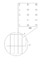
図2は、アライメントスコープ19の配置、およびモールドMとウエハWとにそれぞれ形成されているモールドM側アライメントマークAMMとウエハW側アライメントマークAMWとを示す図である。特に、図2(a)は、アライメントスコープ19、モールドM、樹脂R、およびウエハWの配置を示す概略断面図である。また、図2(b)は、アライメントマークAMM、AMWをそれぞれ紫外線入射側から見たときの拡大図である。アライメントマークAMMとアライメントマークAMWとは、図2(a)に示す状態でモールドMへの紫外線入射側から見たときに、互いに重ならないように配置される。さらに、図2(c)は、紫外線入射側からモールドMを見たときの複数のアライメントマークAMM、AMWの配置を示す概略平面図である。特に、モールドMの四隅にある領域19a〜19dは、アライメントスコープ19の(特定の)検出対象の位置(検出位置)となる領域である。一方、図3は、ウエハW上のショットの配置を示す平面図である。ウエハWは、その表面上に複数のショットSを含み、各ショットS内に複数のアライメントマークAMWが形成されている。
FIG. 2 is a diagram showing the arrangement of the
制御部7は、インプリント装置1の各構成要素の動作および調整などを制御し得る。制御部7は、例えばコンピュータなどで構成され、インプリント装置1の各構成要素に回線を介して接続され、プログラムなどにしたがって各構成要素の制御を実行し得る。本実施形態の制御部7は、少なくとも、アライメント検出系6、およびウエハステージ4の動作を制御する。なお、制御部7は、インプリント装置1の他の部分と一体で(共通の筐体内に)構成してもよいし、インプリント装置1の他の部分とは別体で(別の筐体内に)構成してもよい。
The
さらに、インプリント装置1は、ウエハステージ4を載置し基準平面を形成する不図示の定盤と、モールド保持機構3を固定するブリッジ定盤15と、定盤から延設され、床面からの振動を除去する除振器を介してブリッジ定盤15を支持する支柱とを備える。さらに、インプリント装置1は、共に不図示であるが、モールドMを装置外部とモールド保持機構3との間で搬入出させるモールド搬送機構や、ウエハWを装置外部とウエハステージ4との間で搬入出させる基板搬送機構などを含み得る。
Further, the
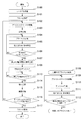
次に、インプリント装置1によるインプリント方法について説明する。図4は、インプリント装置1による一連のインプリント処理の動作シーケンスを示すフローチャートである。まず、制御部7は、モールド搬送機構によりモールドMをモールドチャック13に搬送させ、位置決め後、モールドチャック13にモールドMを保持させる(ステップS100)。ここで、制御部7は、モールドMの設置後、アライメントステージ機構20によりアライメントスコープ19を移動させる。特に本実施形態では、制御部7は、アライメントスコープ19による検出位置が、図2(c)に示すようなショットの四隅にある領域19a〜19dに位置するように動作させる。
Next, an imprint method by the
次に、制御部7は、基板搬送機構によりウエハWをウエハチャック17に搬送し、ウエハチャック17によりウエハWを保持させる(ステップS101)。ここで、ウエハWには少なくとも1層のパターンがアライメントマークAMWとともに予め形成されていることとする。制御部7は、アライメントスコープ19により、モールドMのアライメントマークAMMを透過して、このアライメントマークAMMとウエハWのアライメントマークAMWとの相対位置を計測させることとなる。
Next, the
次に、制御部7は、アライメントステージ機構20により、アライメントスコープ19の移動を開始させる(ステップS102)。次に、制御部7は、アライメントスコープ19の移動と同時に、今回の処理対象となるショットが塗布部5の塗布位置に位置するようにウエハステージ4を駆動させ、塗布部5により樹脂Rを塗布させる(ステップS103:塗布工程)。さらに、制御部7は、ショットがモールドMとの押し付け位置に位置するようにウエハステージ4を駆動させる。
Next, the
次に、制御部7は、ダイバイダイアライメント方式によりアライメント計測を実施させる(ステップS104)。このとき、制御部7は、アライメントスコープ19によりモールドMとウエハWとの各アライメントマークAMM、AMWを撮像し、不図示の画像処理装置により各アライメントマークAMM、AMWの相対位置を計測する。そして、制御部7は、各領域19a〜19dに対応した4つの位置における検出結果に基づいてモールドMとウエハWとのショット形状の差(座標、回転、倍率、台形成分など)を計測する。
Next, the
次に、制御部7は、位置合わせと同時に、必要に応じて、モールドMに形成されているパターン部の形状とウエハWのショット形状(基板側パターンの形状)とを合わせるために、倍率補正機構16によりモールドMの形状を補正する(ステップS105)。次に、制御部7は、倍率補正機構16の駆動誤差などにより誤差が生じる可能性があるため、形状差のトレランス判定を行う(ステップS106)。ここで、制御部7は、形状差がトレランス以上と判定した場合には(NO)、ステップS104の戻り、アライメントの再計測を実施させ、形状差が予め定められたトレランス以下になるまでモールドMの形状補正を実施させる。一方、制御部7は、ステップS106にて形状差がトレランス以下であると判定した場合には(YES)、次に、押し付け動作を開始させる(ステップS107:押型工程)。
Next, at the same time as positioning, the
次に、制御部7は、さらに精密な形状補正のため、押し付け動作中、すなわちモールドMへの樹脂Rの充填中も順次アライメント計測を行う(ステップS108)。図5は、押し付け時の樹脂Rの充填状態、およびこの充填状態に伴うアライメント計測の検出位置を時系列に示す平面図である。このとき、アライメント計測の検出位置は、変更可能であり、図5における検出位置は、一例である。まず、制御部7は、以下に示すように、計測した値を統計処理し、ショットの変形分の補正値を算出し、位置合わせを行う。図5に示すように、充填される樹脂Rの接触領域は、接触が始まった中心から放射状に外側へ広がっていくことが分かる。このとき、樹脂Rの充填が完了した部分と完了していない部分では、例えば、色が異なっていたり、樹脂Rの屈折率などにより、計測条件が一定でない。そのため、樹脂Rの充填が完了した部分と完了していない部分との境界上のアライメントマークAMM、AMWの計測データを補正に利用することはできない。したがって、制御部7は、樹脂Rの充填が完了したショット中心付近の領域19eから放射状に外側に向かって順番に、樹脂Rの充填に合わせてアライメントスコープ19を移動させ(ステップS109)、領域19f〜19qの計測をさせる(ステップS110)。その際、制御部7は、樹脂Rの充填が完了した位置を判定するために、ショット全体を観察する観察スコープ12を用いる。
Next, the
まず、図5(a)に示す樹脂Rの充填の状態で、アライメントスコープ19は、充填が完了したショット中心の領域19eでアライメント計測する。次に、図5(b)および(c)に示す樹脂Rの充填の状態で、アライメントスコープ19は、樹脂Rの充填が完了した状態に合わせて順番に領域19f〜19mでアライメント計測する。最終的に充填が完了した図5(d)に示す樹脂Rの充填が完了した状態で、アライメントスコープ19は、ショットの一番外側の領域19n〜19qでアライメント計測する。このように、インプリント装置1は、複数(4つ以上)の位置で(本実施形態では、領域19e〜19qで)アライメント計測を行うので、より精密な補正量を取得できる。また、制御部7は、観察スコープ12によって最初のショットであらかじめ樹脂Rの広がりの時間を計測することにより、次ショット以降の計測するアライメントマークAMM、AMWの位置を決定することができる。したがって、観察スコープ12による樹脂Rの充填完了の確認動作を省略することが可能である。また、樹脂Rの充填中の補正に関しては、アライメントマークAMM、AMWの計測ごとに行ってもよく、すべてのアライメントマークAMM、AMWの計測が完了した後に行ってもよい。そして、制御部7は、必要に応じてモールドMに形成されているパターン部の形状とウエハWのショット形状とを合わせるため、倍率補正機構16によりモールドMの形状を補正する(ステップS111)。
First, in a state where the resin R is filled as shown in FIG. 5A, the
次に、制御部7は、樹脂Rの充填している範囲にある検出対象となるアライメントマークAMM、AMWの計測がすべて完了したかどうかの判定を行う(ステップS112)。ここで、制御部7は、検出対象となるアライメントマークAMM、AMWの計測がすべて完了したと判定した場合(YES)、充填中のアライメントを終了し、ステップS114へ移行する。一方、制御部7は、検出対象となるアライメント計測がすべて完了していないと判定した場合(NO)、ステップS109へ戻り、検出対象となるアライメント計測がすべて完了するまで、繰り返しアライメント計測を行う。
Next, the
次に、制御部7は、押し付け動作が完了したか(モールドMへの樹脂Rの充填が完了したか)を判定する(ステップS113)。ここで、制御部7は、充填が完了してない間、すなわち充填が完了していないと判定した場合には(NO)、充填が完了するまで、繰り返し判定を行う。一方、制御部7は、充填が完了したと判定した場合には(YES)、光照射部2によりモールドMを介してウエハW上の樹脂Rに紫外線10を照射させ、樹脂Rを硬化させる(ステップS114:硬化工程)。樹脂Rの硬化後、制御部7は、モールド駆動機構14によりモールドMを上昇させ、モールドMと硬化した樹脂Rとを引き離す(ステップ115:離型工程)。
Next, the
次に、制御部7は、ウエハW上の全てのショットに対するインプリント処理(パターン形成工程)が終了したかどうかを判断する(ステップS116)。ここで、制御部7は、インプリント処理がなされていないショットがあると判定した場合には(NO)、ステップS102に戻り次のショットに対する処理を繰り返す。一方、制御部7は、ステップS116にて全てのショットに対するインプリント処理が完了していると判定した場合には(YES)、基板搬送機構によりウエハWをウエハチャック17から回収し(ステップS117)、全ての処理を終了する。
Next, the
このように、制御部7は、押し付け動作をしている間(モールドMへ樹脂Rを充填している間)に、樹脂Rの充填状態に合わせてアライメントスコープ19を駆動させ、4つ以上の複数の検出位置でアライメント計測を行う。ここで、モールドMのパターン部(凹凸パターン)に樹脂Rを充填している間、樹脂Rの充填が完了している部分と完了していない部分とでは、計測条件が異なり、計測値を補正に使用することができない。これに対して、本実施形態では、より多くの位置でアライメント計測を行うことにより、線形成分だけでなく高次成分の補正を行うことができるので、重ね合わせの精度をより向上させることができる。また、本実施形態では、制御部7は、観察スコープ12を用いて、樹脂Rの充填が完了したことを確認しながら、モールドMの中心から外側へ放射状に、樹脂Rの充填が完了した位置からアライメント計測を行う。したがって、観察スコープ12による樹脂Rの充填完了の確認動作を省略することができる。さらに、アライメント計測および補正のための時間が、押し付け時間(樹脂Rの充填時間)と重なる、すなわち隠れるため、インプリント処理全体の処理時間が増えることはない。したがって、インプリント処理全体の処理時間が変わることなく、重ね合わせの精度を向上させることができる。
As described above, the
以上のように、本実施形態によれば、インプリント処理時の重ね合わせ精度の向上に有利なインプリント方法を提供することができる。 As described above, according to the present embodiment, it is possible to provide an imprint method that is advantageous for improving the overlay accuracy during imprint processing.
なお、上記実施形態では、制御部7は、検出対象となるアライメントマークAMM、AMWのすべての計測後、樹脂Rの充填完了を待って硬化を行うとしたが、充填完了を待っている間にアライメント計測を継続し、位置合わせと形状補正とを続けてもよい。制御部7は、樹脂Rの充填の進行に合わせてアライメントスコープ19を移動させていたが、ショットの形状やモールドMの形状が安定している場合は、ショット中心付近のアライメントマークAMM、AMWのみを計測し補正を行ってもよい。
In the above embodiment, the
さらに、上記実施形態では、制御部7は、充填中にアライメントマークAMM、AMWを計測する際、アライメントスコープ19の移動を、移動距離が最短となるような順番で計測すると、全体のインプリント処理時間をより短縮することが可能となる。また、樹脂Rの充填中のアライメント計測の際、アライメントスコープ19の代わりに観察スコープ12を使用することで、アライメントスコープ19の移動時間を必要としないため、さらに時間短縮が可能となる。
Further, in the above embodiment, when the
(物品の製造方法)
物品としてのデバイス(半導体集積回路素子、液晶表示素子等)の製造方法は、上述したインプリント装置を用いて基板(ウエハ、ガラスプレート、フィルム状基板)にパターンを形成する工程を含む。さらに、該製造方法は、パターンを形成された基板をエッチングする工程を含み得る。なお、パターンドメディア(記録媒体)や光学素子などの他の物品を製造する場合には、該製造方法は、エッチングの代わりにパターンを形成された基板を加工する他の処理を含み得る。本実施形態の物品の製造方法は、従来の方法に比べて、物品の性能・品質・生産性・生産コストの少なくとも1つにおいて有利である。
(Product manufacturing method)
A method for manufacturing a device (semiconductor integrated circuit element, liquid crystal display element, etc.) as an article includes a step of forming a pattern on a substrate (wafer, glass plate, film-like substrate) using the above-described imprint apparatus. Furthermore, the manufacturing method may include a step of etching the substrate on which the pattern is formed. In the case of manufacturing other articles such as patterned media (recording media) and optical elements, the manufacturing method may include other processes for processing a substrate on which a pattern is formed instead of etching. The method for manufacturing an article according to the present embodiment is advantageous in at least one of the performance, quality, productivity, and production cost of the article as compared with the conventional method.
以上、本発明の好ましい実施形態について説明したが、本発明は、これらの実施形態に限定されず、その要旨の範囲内で種々の変形および変更が可能である。 As mentioned above, although preferable embodiment of this invention was described, this invention is not limited to these embodiment, A various deformation | transformation and change are possible within the range of the summary.
M モールド
W ウエハ
R 樹脂
AMM アライメントマーク
AMW アライメントマーク
M Mold W Wafer R Resin AMM Alignment mark AMW Alignment mark
Claims (15)
前記型と前記インプリント材とを接触させ、前記型と前記インプリント材との接触領域を広げる工程と、
前記接触領域の広がりに応じてアライメントマークを検出する検出器の位置を変化させることにより、前記基板上の互いに異なる場所に形成された複数の前記アライメントマークを順次検出する工程と、
を含むことを特徴とするインプリント方法。 A imprint method of forming a pattern of an imprint material on a substrate using a mold,
And then contacting the mold and before Symbol imprint material, Ru widened contact area between the imprint material and the mold process,
Sequentially detecting a plurality of alignment marks formed at different locations on the substrate by changing the position of a detector that detects the alignment marks according to the spread of the contact area ;
The imprint method characterized by including.
前記型の複数の領域を前記基板上の前記インプリント材に順次、接触させる工程と、
前記接触させる工程にて、前記型の複数の領域のうち、先に接触する領域に形成されたアライメントマークを検出器が検出した後、前記検出器の位置を変化させ、前記型の複数の領域のうち、後に接触する領域に形成されたアライメントマークを検出する工程と、
を含むことを特徴とするインプリント方法。 A imprint method of forming a pattern of an imprint material on a substrate using a mold,
Sequentially a plurality of regions of the mold before Symbol imprint material on the substrate, and the step of contacting,
In the step of contacting, after the detector detects an alignment mark formed in the first contact region among the plurality of regions of the mold, the position of the detector is changed, and the plurality of regions of the mold A step of detecting an alignment mark formed in a region to be contacted later,
The imprint method characterized by including.
前記基板上のアライメントマークを検出する検出器と、
前記型と前記基板上のインプリント材とを接触させる際、前記検出器の位置を、前記型と前記インプリント材との接触する接触領域の広がりに応じて変化させながら、複数の前記アライメントマークを検出させる制御部と、
を備えるインプリント装置。 A imprint apparatus for forming a pattern of an imprint material on a substrate using a mold,
A detector for detecting the A line placement mark on the substrate,
When contacting the Lee down printed material on the substrate and the mold, the position of the detector, while changing in accordance with the extent of the contact region contacting with the mold and the imprint material, a plurality of the alignment A control unit for detecting a mark;
An imprint apparatus comprising:
を含むことを特徴とする物品の製造方法。 As engineering to form a pattern of the imprint material on a substrate using an imprint method according to any one of claims 1 to 12
A method for producing an article comprising:
Priority Applications (6)
| Application Number | Priority Date | Filing Date | Title |
|---|---|---|---|
| JP2013041424A JP6029494B2 (en) | 2012-03-12 | 2013-03-04 | Imprint method, imprint apparatus, and article manufacturing method using the same |
| PCT/JP2013/001435 WO2013136730A1 (en) | 2012-03-12 | 2013-03-07 | Imprint method, imprint apparatus, and article manufacturing method using the same |
| KR1020147024456A KR101666288B1 (en) | 2012-03-12 | 2013-03-07 | Imprint method, imprint apparatus, and article manufacturing method using the same |
| US14/376,221 US10901324B2 (en) | 2012-03-12 | 2013-03-07 | Imprint method, imprint apparatus, and article manufacturing method using the same |
| CN201380013086.5A CN104160477B (en) | 2012-03-12 | 2013-03-07 | Method for stamping, imprinting apparatus and use its article manufacturing method |
| EP13760734.7A EP2791966B1 (en) | 2012-03-12 | 2013-03-07 | Imprint method, imprint apparatus, and article manufacturing method using the same |
Applications Claiming Priority (3)
| Application Number | Priority Date | Filing Date | Title |
|---|---|---|---|
| JP2012053993 | 2012-03-12 | ||
| JP2012053993 | 2012-03-12 | ||
| JP2013041424A JP6029494B2 (en) | 2012-03-12 | 2013-03-04 | Imprint method, imprint apparatus, and article manufacturing method using the same |
Publications (3)
| Publication Number | Publication Date |
|---|---|
| JP2013219331A JP2013219331A (en) | 2013-10-24 |
| JP2013219331A5 JP2013219331A5 (en) | 2016-04-21 |
| JP6029494B2 true JP6029494B2 (en) | 2016-11-24 |
Family
ID=49160663
Family Applications (1)
| Application Number | Title | Priority Date | Filing Date |
|---|---|---|---|
| JP2013041424A Active JP6029494B2 (en) | 2012-03-12 | 2013-03-04 | Imprint method, imprint apparatus, and article manufacturing method using the same |
Country Status (6)
| Country | Link |
|---|---|
| US (1) | US10901324B2 (en) |
| EP (1) | EP2791966B1 (en) |
| JP (1) | JP6029494B2 (en) |
| KR (1) | KR101666288B1 (en) |
| CN (1) | CN104160477B (en) |
| WO (1) | WO2013136730A1 (en) |
Families Citing this family (11)
| Publication number | Priority date | Publication date | Assignee | Title |
|---|---|---|---|---|
| JP6472189B2 (en) * | 2014-08-14 | 2019-02-20 | キヤノン株式会社 | Imprint apparatus, imprint method, and article manufacturing method |
| JP2016134441A (en) * | 2015-01-16 | 2016-07-25 | キヤノン株式会社 | Imprint device, imprint method, and manufacturing method of article |
| JP6671160B2 (en) | 2015-11-30 | 2020-03-25 | キヤノン株式会社 | Imprint apparatus, article manufacturing method and alignment method |
| JP6748496B2 (en) * | 2016-06-30 | 2020-09-02 | キヤノン株式会社 | Mold, imprint method, imprint apparatus, and article manufacturing method |
| JP6716484B2 (en) * | 2017-03-14 | 2020-07-01 | キオクシア株式会社 | Imprint method |
| JP2018194386A (en) * | 2017-05-16 | 2018-12-06 | 大日本印刷株式会社 | Sensor module |
| JP6865650B2 (en) * | 2017-07-27 | 2021-04-28 | キヤノン株式会社 | Imprint equipment and article manufacturing method |
| JP7033994B2 (en) * | 2018-04-11 | 2022-03-11 | キヤノン株式会社 | Molding equipment and manufacturing method of articles |
| JP7317575B2 (en) * | 2019-05-28 | 2023-07-31 | キヤノン株式会社 | IMPRINT APPARATUS, IMPRINT METHOD, AND ARTICLE MANUFACTURING METHOD |
| JP2021044296A (en) * | 2019-09-06 | 2021-03-18 | キオクシア株式会社 | Imprint method, manufacturing method for semiconductor device, and imprint device |
| ES2817099B2 (en) * | 2020-11-10 | 2021-08-30 | Rudatskiy Sergii Birzhev | DIGITAL TRANSFORMABLE MOLD |
Family Cites Families (13)
| Publication number | Priority date | Publication date | Assignee | Title |
|---|---|---|---|---|
| DE10146583A1 (en) * | 2001-09-21 | 2003-04-17 | Siemens Ag | Device and method for optically scanning a substrate wafer |
| JP2006165371A (en) * | 2004-12-09 | 2006-06-22 | Canon Inc | Transfer apparatus and device manufacturing method |
| CN1800975B (en) | 2005-11-28 | 2011-11-30 | 中国科学院光电技术研究所 | Stepped and repeated illuminating and nano-imprinting device |
| JP4827513B2 (en) | 2005-12-09 | 2011-11-30 | キヤノン株式会社 | Processing method |
| JP4185941B2 (en) * | 2006-04-04 | 2008-11-26 | キヤノン株式会社 | Nanoimprint method and nanoimprint apparatus |
| US9573319B2 (en) | 2007-02-06 | 2017-02-21 | Canon Kabushiki Kaisha | Imprinting method and process for producing a member in which a mold contacts a pattern forming layer |
| EP2128701A1 (en) * | 2008-05-30 | 2009-12-02 | ASML Netherlands BV | Method of determining defects in a substrate and apparatus for exposing a substrate in a lithographic process |
| JP5279397B2 (en) | 2008-08-06 | 2013-09-04 | キヤノン株式会社 | Imprint apparatus, imprint method, and device manufacturing method |
| JP2010214913A (en) * | 2009-03-19 | 2010-09-30 | Toppan Printing Co Ltd | Imprinting method and imprinting device |
| JP2011129720A (en) | 2009-12-17 | 2011-06-30 | Canon Inc | Imprint device, mold, and method of manufacturing article |
| JP5451450B2 (en) * | 2010-02-24 | 2014-03-26 | キヤノン株式会社 | Imprint apparatus, template thereof, and article manufacturing method |
| US9430824B2 (en) * | 2013-05-14 | 2016-08-30 | Kla-Tencor Corporation | Machine learning method and apparatus for inspecting reticles |
| JP5909210B2 (en) * | 2013-07-11 | 2016-04-26 | キヤノン株式会社 | Imprint apparatus and article manufacturing method |
-
2013
- 2013-03-04 JP JP2013041424A patent/JP6029494B2/en active Active
- 2013-03-07 CN CN201380013086.5A patent/CN104160477B/en active Active
- 2013-03-07 KR KR1020147024456A patent/KR101666288B1/en active IP Right Grant
- 2013-03-07 EP EP13760734.7A patent/EP2791966B1/en active Active
- 2013-03-07 US US14/376,221 patent/US10901324B2/en active Active
- 2013-03-07 WO PCT/JP2013/001435 patent/WO2013136730A1/en active Application Filing
Also Published As
| Publication number | Publication date |
|---|---|
| JP2013219331A (en) | 2013-10-24 |
| EP2791966A1 (en) | 2014-10-22 |
| KR101666288B1 (en) | 2016-10-13 |
| EP2791966A4 (en) | 2015-07-29 |
| KR20140119800A (en) | 2014-10-10 |
| WO2013136730A1 (en) | 2013-09-19 |
| CN104160477B (en) | 2016-11-09 |
| EP2791966B1 (en) | 2020-02-26 |
| US10901324B2 (en) | 2021-01-26 |
| US20150325526A1 (en) | 2015-11-12 |
| CN104160477A (en) | 2014-11-19 |
Similar Documents
| Publication | Publication Date | Title |
|---|---|---|
| JP6029494B2 (en) | Imprint method, imprint apparatus, and article manufacturing method using the same | |
| JP6029495B2 (en) | Imprint method, imprint apparatus, and article manufacturing method using the same | |
| KR102017906B1 (en) | Pattern formation method, lithography apparatus, lithography system, and article manufacturing method | |
| JP5662741B2 (en) | Imprint apparatus and article manufacturing method | |
| JP6333039B2 (en) | Imprint apparatus, device manufacturing method, and imprint method | |
| CN110083009B (en) | Imprint method, imprint apparatus, and device manufacturing method | |
| US10018910B2 (en) | Imprint apparatus, alignment method, and method of manufacturing article | |
| JP6457773B2 (en) | Imprint method, imprint apparatus and article manufacturing method | |
| JP2016063219A (en) | Imprint device, imprint system, and product manufacturing method | |
| JP2016018824A (en) | Imprint device and method of manufacturing article | |
| JP6178694B2 (en) | Imprint apparatus and article manufacturing method | |
| JP2017123493A (en) | Imprint method, imprint device, and device manufacturing method | |
| JP6792669B2 (en) | Pattern formation method, lithography equipment, lithography system and article manufacturing method | |
| JP6866106B2 (en) | Imprinting equipment, imprinting methods, and manufacturing methods for goods | |
| US11833737B2 (en) | Imprint apparatus, method of imprinting, and method of manufacturing article | |
| KR20230152569A (en) | Lithography device, lithography method, and article manufacturing method |
Legal Events
| Date | Code | Title | Description |
|---|---|---|---|
| A521 | Request for written amendment filed |
Free format text: JAPANESE INTERMEDIATE CODE: A523 Effective date: 20160303 |
|
| A621 | Written request for application examination |
Free format text: JAPANESE INTERMEDIATE CODE: A621 Effective date: 20160303 |
|
| TRDD | Decision of grant or rejection written | ||
| A01 | Written decision to grant a patent or to grant a registration (utility model) |
Free format text: JAPANESE INTERMEDIATE CODE: A01 Effective date: 20160920 |
|
| A61 | First payment of annual fees (during grant procedure) |
Free format text: JAPANESE INTERMEDIATE CODE: A61 Effective date: 20161018 |
|
| R151 | Written notification of patent or utility model registration |
Ref document number: 6029494 Country of ref document: JP Free format text: JAPANESE INTERMEDIATE CODE: R151 |