JP6472189B2 - Imprint apparatus, imprint method, and article manufacturing method - Google Patents
Imprint apparatus, imprint method, and article manufacturing method Download PDFInfo
- Publication number
- JP6472189B2 JP6472189B2 JP2014165198A JP2014165198A JP6472189B2 JP 6472189 B2 JP6472189 B2 JP 6472189B2 JP 2014165198 A JP2014165198 A JP 2014165198A JP 2014165198 A JP2014165198 A JP 2014165198A JP 6472189 B2 JP6472189 B2 JP 6472189B2
- Authority
- JP
- Japan
- Prior art keywords
- mold
- substrate
- pattern
- imprint
- imprint material
- Prior art date
- Legal status (The legal status is an assumption and is not a legal conclusion. Google has not performed a legal analysis and makes no representation as to the accuracy of the status listed.)
- Active
Links
Images


Classifications
-
- G—PHYSICS
- G03—PHOTOGRAPHY; CINEMATOGRAPHY; ANALOGOUS TECHNIQUES USING WAVES OTHER THAN OPTICAL WAVES; ELECTROGRAPHY; HOLOGRAPHY
- G03F—PHOTOMECHANICAL PRODUCTION OF TEXTURED OR PATTERNED SURFACES, e.g. FOR PRINTING, FOR PROCESSING OF SEMICONDUCTOR DEVICES; MATERIALS THEREFOR; ORIGINALS THEREFOR; APPARATUS SPECIALLY ADAPTED THEREFOR
- G03F7/00—Photomechanical, e.g. photolithographic, production of textured or patterned surfaces, e.g. printing surfaces; Materials therefor, e.g. comprising photoresists; Apparatus specially adapted therefor
- G03F7/0002—Lithographic processes using patterning methods other than those involving the exposure to radiation, e.g. by stamping
Landscapes
- Physics & Mathematics (AREA)
- General Physics & Mathematics (AREA)
- Shaping Of Tube Ends By Bending Or Straightening (AREA)
- Engineering & Computer Science (AREA)
- Multimedia (AREA)
- Exposure Of Semiconductors, Excluding Electron Or Ion Beam Exposure (AREA)
- Moulds For Moulding Plastics Or The Like (AREA)
- Health & Medical Sciences (AREA)
- Toxicology (AREA)
Description
本発明は、インプリント装置、インプリント方法及び物品の製造方法に関する。 The present invention relates to an imprint apparatus , an imprint method, and an article manufacturing method.
近年、微細なパターンの形成を可能にするインプリント技術は、様々なデバイス(ICやLSIなどの半導体デバイス、液晶デバイス、CCDなどの撮像デバイス、磁気ヘッドなど)などの物品を製造するための技術として注目されている。インプリント技術は、シリコンウエハやガラスプレートなどの基板上の樹脂と微細なパターンが形成されたモールド(型)とを接触させた状態で、樹脂を硬化させて基板上に微細なパターンを転写する。 In recent years, imprint technology that enables the formation of fine patterns is a technology for manufacturing articles such as various devices (semiconductor devices such as IC and LSI, liquid crystal devices, imaging devices such as CCD, magnetic heads, etc.). It is attracting attention as. In the imprint technology, a resin on a substrate such as a silicon wafer or a glass plate is brought into contact with a mold (mold) on which a fine pattern is formed, and the resin is cured to transfer the fine pattern onto the substrate. .
インプリント技術には、幾つかの樹脂硬化法があり、かかる樹脂硬化法の1つとして光硬化法が知られている。光硬化法では、紫外線硬化型の樹脂に透明なモールドを接触させた状態で紫外線を照射し、樹脂を感光及び硬化させてからモールドを剥離する。光硬化法によるインプリント技術は、透明なモールドを介して基板上のアライメントマークを観察することができることなどから、デバイスの製造に適している。 There are several resin curing methods in imprint technology, and a photocuring method is known as one of such resin curing methods. In the photocuring method, ultraviolet rays are irradiated in a state where a transparent mold is brought into contact with an ultraviolet curable resin to expose and cure the resin, and then the mold is peeled off. The imprint technique based on the photocuring method is suitable for manufacturing a device because an alignment mark on a substrate can be observed through a transparent mold.
このようなインプリント技術を用いたインプリント装置においては、基板上の硬化した樹脂からモールドを剥離する離型が課題とされている。離型が正しく行われない場合、基板上の硬化した樹脂がちぎれたり、モールドのパターン(凹部)に樹脂が残存して目詰まりが発生したり、モールドや基板が所定の位置からずれたり(又は変形したり)してしまうことがある。これらは、物品の歩留まりやインプリント装置の稼働率の低下を招くことになる。 In an imprint apparatus using such an imprint technique, it is a problem to release a mold from a cured resin on a substrate. If the mold release is not performed correctly, the cured resin on the substrate may be torn off, the resin may remain in the mold pattern (recess) and clogging may occur, or the mold or substrate may be displaced from a predetermined position (or Deformation). These lead to a decrease in the yield of articles and the operating rate of the imprint apparatus.
従って、離型が正しく行われることが物品の歩留まりやインプリント装置の稼働率の向上につながり、そのための技術が幾つか提案されている(特許文献1及び2参照)。特許文献1には、インプリント装置の外部でモールドのパターン面に界面活性剤(離型剤)を塗布してモールドと樹脂との間の接着性を低減する技術が開示されている。また、特許文献2には、離型に要する力を計測する計測部をインプリント装置に設け、かかる力が閾値を超えた場合に離型剤を基板に塗布してモールドと樹脂との間の接着性を低減する技術が開示されている。 Therefore, the correct mold release leads to an improvement in the yield of articles and the operating rate of the imprint apparatus, and several techniques for that have been proposed (see Patent Documents 1 and 2). Patent Document 1 discloses a technique for reducing the adhesion between a mold and a resin by applying a surfactant (release agent) to the pattern surface of the mold outside the imprint apparatus. Further, in Patent Document 2, a measurement unit that measures a force required for mold release is provided in the imprint apparatus, and when the force exceeds a threshold value, a release agent is applied to the substrate and the mold and the resin are separated. Techniques for reducing adhesion are disclosed.
しかしながら、従来技術では、基板上に形成されるパターンの欠陥発生率を低減することはできるが、モールドと樹脂との剥離状態を把握することが困難であり、離型に異常があった場合には、物品の歩留まりやインプリント装置の稼働率に影響を及ぼしてしまう。特に、離型の異常は様々な要因によって引き起こされるため、その要因を特定するためには、モールドと基板との剥離状態を把握(評価)することが必要となる。一方、離型に要する力を計測することでモールドと基板との剥離状態を推測することは可能であるが、その精度は低く、また、閾値の設定に困難な作業を要する。 However, the conventional technology can reduce the defect occurrence rate of the pattern formed on the substrate, but it is difficult to grasp the peeling state between the mold and the resin, and there is an abnormality in the mold release. Affects the yield of articles and the operating rate of the imprint apparatus. In particular, since abnormalities of mold release are caused by various factors, it is necessary to grasp (evaluate) the peeling state between the mold and the substrate in order to identify the factors. On the other hand, it is possible to estimate the peeled state between the mold and the substrate by measuring the force required for mold release, but the accuracy is low, and it is difficult to set the threshold value.
本発明は、このような従来技術の課題に鑑みてなされ、基板上の硬化したインプリント材からモールドを剥離している間におけるモールドとインプリント材との剥離状態を評価するのに有利なインプリント装置を提供することを例示的目的とする。 The present invention has been made in view of such problems of the prior art, and is an imprint that is advantageous for evaluating the peeled state between the mold and the imprint material while the mold is peeled from the cured imprint material on the substrate. It is an exemplary object to provide a printing device.
上記目的を達成するために、本発明の一側面としてのインプリント装置は、基板上にモールドを用いてインプリント材のパターンを形成するインプリント装置であって、前記インプリント材を硬化させる硬化部と、前記モールドと前記基板とを相対的に移動させる移動部と、前記モールドで反射された光と前記基板で反射された光のパターンを検出する検出部と、前記移動部によって前記モールドと前記基板との間隔を広げることで前記基板上の硬化したインプリント材から前記モールドを剥離している間において前記検出部によって検出されたパターンに基づいて、前記モールドと前記インプリント材との剥離状態に関する情報を求める処理部と、を有し、前記検出部は、前記光のパターンに含まれる複数の干渉縞を検出し、前記処理部は、前記情報として、前記複数の干渉縞の間隔に基づいて、前記基板上の硬化したインプリント材から前記モールドを剥離している間における前記モールドの変形量を求めることを特徴とする。 In order to achieve the above object, an imprint apparatus according to one aspect of the present invention is an imprint apparatus that forms a pattern of an imprint material on a substrate using a mold, and cures the imprint material. A moving unit that relatively moves the mold and the substrate, a detection unit that detects a pattern of light reflected by the mold and a light reflected by the substrate, and the mold by the moving unit. The mold and the imprint material are peeled based on the pattern detected by the detection unit while the mold is peeled from the cured imprint material on the substrate by widening the gap with the substrate. possess a processing unit for obtaining information on the state, and the detection unit detects a plurality of interference fringe contained in the pattern of the light, the processing unit As the information, based on the interval of the plurality of interference fringes, and obtains the amount of deformation of the mold at while separating the mold from the cured imprint material on the substrate.
本発明の更なる目的又はその他の側面は、以下、添付図面を参照して説明される好ましい実施形態によって明らかにされるであろう。 Further objects and other aspects of the present invention will become apparent from the preferred embodiments described below with reference to the accompanying drawings.
本発明によれば、例えば、基板上の硬化したインプリント材からモールドを剥離している間におけるモールドとインプリント材との剥離状態を評価するのに有利なインプリント装置を提供することができる。 According to the present invention, for example, it is possible to provide an imprint apparatus that is advantageous for evaluating a peeling state between a mold and an imprint material while the mold is peeled from a cured imprint material on a substrate. .
以下、添付図面を参照して、本発明の好適な実施の形態について説明する。なお、各図において、同一の部材については同一の参照番号を付し、重複する説明は省略する。 DESCRIPTION OF EXEMPLARY EMBODIMENTS Hereinafter, preferred embodiments of the invention will be described with reference to the accompanying drawings. In addition, in each figure, the same reference number is attached | subjected about the same member and the overlapping description is abbreviate | omitted.
<第1の実施形態>
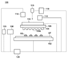
図1、図2及び図3は、本発明の一側面としてのインプリント装置100の構成を示す概略図である。インプリント装置100は、基板上のインプリント材をモールドで成形して基板上にパターンを形成するインプリント処理を行うリソグラフィ装置である。インプリント装置100は、インプリント材として樹脂を採用し、樹脂硬化法として紫外線の照射によって樹脂を硬化させる光硬化法を採用する。
<First Embodiment>
1, 2 and 3 are schematic views showing the configuration of an
インプリント装置100は、基板ステージ102と、モールドステージ106と、樹脂供給部108と、移動部110と、光源112と、スコープ114と、検出部116と、処理部118と、塗布部119と、制御部120とを有する。
The
基板ステージ102は、基板チャックを介して、シリコンウエハやガラスプレートなどの基板STを保持して移動する。基板ステージ102は、基板STを所定の位置に位置決めする。基板ステージ102の移動は、例えば、リニアモータなどのアクチュエータの駆動によって行われる。
The
モールド104は、光源112からの紫外線を透過する材料、例えば、石英で構成され、基板STに転写すべきパターン(凹凸パターン)が形成されたパターン面104aを有する。モールド104は、モールドチャックを介して、モールドステージ106に保持される。
The
樹脂供給部108は、樹脂RSを液滴として吐出する複数のディスペンサを含み、基板上(パターンを形成すべきショット領域)に樹脂RSを供給(塗布)する。具体的には、樹脂供給部108を構成するディスペンサから樹脂RSを吐出しながら基板ステージ102を移動(スキャン移動やステップ移動)させることで、基板上に樹脂RSを塗布することが可能となる。
The
移動部110は、エアシリンダやリニアモータなどで構成されたアクチュエータを含み、モールド104を保持したモールドステージ106、即ち、モールド104を移動させる。移動部110は、図2に示すように、モールド104を下方向に移動させる(即ち、モールド104と基板STとの間隔を狭める)ことで、モールド104と基板上の樹脂RSとを接触させる。また、移動部110は、図3に示すように、モールド104を上方向に移動させる(即ち、モールド104と基板STとの間隔を広げる)ことで、基板上の硬化した樹脂RSからモールド104を剥離(離型)する。このように、移動部110は、モールド104と基板STとを相対的に移動させる機能を有する。但し、基板STを保持する基板ステージ102、即ち、基板STを上下方向に移動させること、或いは、モールド104と基板STの両方を上下方向に移動させることで、モールド104と基板STとを相対的に移動させてもよい。
The moving
光源112は、モールド104と基板上の樹脂RSとを接触させた状態において、モールド104を介して、樹脂RSに紫外線を照射し、樹脂RSを硬化させる。換言すれば、光源112は、基板上の樹脂RSを硬化させる硬化部として機能する。
In a state where the
スコープ114は、基板STに設けられたアライメントマークやモールド104に設けられたアライメントマークを検出する。また、スコープ114は、基板ステージ102に設けられた基準マークなども検出することが可能である。
The
検出部116は、波長範囲の狭い帯域の光(照明光)を放射する光源、例えば、ハロゲンランプ、キセノンランプ、メタルハライドランプなどの放射ランプを含む。検出部116は、モールド104と基板STとの剥離状態に関する情報を得るために、モールド104で反射された光と基板STで反射された光との干渉パターン(干渉縞、所謂、ニュートンリング)を検出する。
The
モールド104と基板STとの間のギャップをd、照明光の波長をλとする。この場合、2d=mλ(mは自然数)を満たすときに、モールド104で反射された光と基板STで反射された光とが打ち消し合うため、検出部116では暗リングが検出される。また、2d=(m+1/2)λを満たすときに、モールド104で反射された光と基板STで反射された光とが強め合うため、検出部116では明リングが検出される。従って、広帯域の白色光で照明すると、検出部116で検出される干渉パターンのピッチが波長ごとに少しずつずれて重なり合うため、干渉パターンのコントラストを低下させてしまう。そのため、検出部116では、照明光として、波長範囲の狭い帯域の光を用いている。
The gap between the
処理部118は、基板上の硬化した樹脂RSからモールド104を剥離している間において検出部116によって検出された干渉パターンに基づいて、モールド104と樹脂RSとの剥離状態に関する情報を求める。
The
基板上の硬化した樹脂RSからモールド104を剥離するために、移動部110によってモールド104を上方向に移動させると、モールド104と基板STとの間にギャップが生じる。この際、検出部116は、モールド104と基板STとの間のギャップに対応する干渉パターンを検出する。ここで、基板上の硬化した樹脂RSからモールド104を剥離する際、基板STは、ほぼ変形しないとみなすことができる。従って、処理部118は、モールド104と基板STとの間のギャップに対応する干渉パターンから、モールド104と樹脂RSとの剥離状態に関する情報として、モールド104の形状、即ち、モールド104の変形量を求めることができる。
When the
図4は、モールド104と基板STとの間のギャップと、検出部116によって検出される干渉パターンとを示す図である。図4を参照するに、ギャップd1及びd2において暗リングが検出され、処理部118は、かかる暗リングからモールド104の形状、即ち、モールド104の変形量を求めることができる。また、処理部118は、図4に示す干渉パターンから、樹脂RSとモールド104とが剥離している領域と樹脂RSとモールド104とが剥離していない領域との境界の位置EXFを求めることもできる。境界の位置EXFは、モールド104が樹脂RSから剥離した位置(剥離位置)であって、モールド104と樹脂RSとの剥離状態に関する情報の一例である。
FIG. 4 is a diagram illustrating a gap between the
塗布部119は、モールド104と基板上の硬化した樹脂RSとの間の接着性を低減するために、モールド104のパターン面104aに界面活性剤(離型剤)を塗布する。但し、塗布部119は、インプリント装置100に必須の構成要素ではなく、例えば、インプリント装置100の外部でモールド104のパターン面104aに界面活性剤を塗布してもよい。
The
制御部120は、CPUやメモリを含み、インプリント装置100の各部を制御して、インプリント装置100を動作させる。例えば、制御部120は、基板上の樹脂RSをモールド104で成形して基板上にパターンを形成するインプリント処理をインプリント装置100の各部に行わせる。また、制御部120は、処理部118によって求められたモールド104と樹脂RSとの剥離状態に関する情報に基づいて、基板上の硬化した樹脂RSからモールド104が正常に剥離されたかどうかを評価する。制御部120は、基板上の硬化した樹脂RSからモールド104が正常に剥離されていないと評価した場合に、即ち、離型に問題があった場合に、基板STの次のショット領域に対するインプリント処理を停止する。
The
ここで、検出部116によって検出される干渉パターンと、処理部118によって求められるモールド104と樹脂RSとの剥離状態に関する情報との関係について説明する。インプリント処理では、まず、移動部110によってモールド104を下方向に移動させて、モールド104と基板上の樹脂RSとを接触させる。次いで、モールド104と基板上の樹脂RSとを接触させた状態で、光源112からの紫外線を樹脂RSに照射して樹脂RSを硬化させる。次に、移動部110によってモールド104を上方向に移動させて(即ち、モールド104と基板STとの間にギャップを生じさせて)、基板上の硬化した樹脂RSからモールド104を剥離する。
Here, the relationship between the interference pattern detected by the
図5(a)乃至図5(d)は、基板上の硬化した樹脂RSからモールド104を剥離している間における干渉パターンの変化を示す図である。図5(a)乃至図5(d)のそれぞれには、モールド104、基板ST及び樹脂RSの断面を直交する2つの方向の側面から示し、且つ、その時の剥離の進行に応じて検出部116によって検出される干渉パターンを示している。
FIG. 5A to FIG. 5D are diagrams showing a change in the interference pattern while the
図5(a)は、モールド104と基板上の樹脂RSとを接触させた状態で樹脂RSを硬化させたときの状態を示している。この際、モールド104のパターン面104aの全面が樹脂RSと密着しており、モールド104と樹脂RSとの間にギャップが生じていないため、干渉パターンは検出されない。
FIG. 5A shows a state where the resin RS is cured while the
次いで、モールド104を上方向に移動させると、図5(b)に示すように、モールド104のパターン面104aの周辺部の一部が樹脂RSから剥離した状態となるため、モールド104が樹脂RSから剥離した箇所において干渉パターンが検出される。更に、モールド104を上方向に移動させると、図5(c)に示すように、樹脂RSからのモールド104のパターン面104aの剥離が進行して、モールド104の形状(変形)に対応する干渉パターンが検出される。かかる干渉パターンは、1つ以上の干渉縞を含み、モールド104のパターン面104aの中心部から楕円状に検出される。そして、モールド104のパターン面104aの全面が樹脂RSから剥離されると、図5(d)に示すように、干渉パターンが検出されなくなる。
Next, when the
このように、基板上の硬化した樹脂RSからモールド104を剥離する過程において、検出部116によって検出された干渉パターンを解析することで、モールド104と樹脂RSとの剥離状態に関する情報を求めることができる。具体的には、本発明者らは、基板STのショット領域の中心、詳細には、ショット領域の重心位置から対称に干渉縞が検出されると、モールド104のパターンの目詰まりが発生せず、樹脂RSのパターンが破損せずに基板上に形成されることを見出した。
As described above, in the process of peeling the
図6(a)及び図6(b)のそれぞれは、基板STの内部のショット領域FF及び基板STの外周部のショット領域PFにおいて樹脂RSからモールド104を剥離しているときの干渉パターンを示す図である。図6(a)及び図6(b)のそれぞれには、モールド104、基板ST及び樹脂RSの断面を直交する2つの方向の側面から示し、且つ、その時に応じて検出部116によって検出される干渉パターンを示している。
Each of FIG. 6A and FIG. 6B shows an interference pattern when the
図6(a)及び図6(b)を参照するに、ショット領域FF及びFPのいずれにおいても、その重心位置BPから対称に干渉縞が検出されれば、樹脂RSからモールド104が正常に剥離されたと評価することができる。ここでは、基板STの基準位置としてのショット領域の重心位置BPから干渉パターンに含まれる各干渉縞までの距離を、モールド104と樹脂RSとの剥離状態に関する情報とする。具体的には、各干渉縞の上下左右の端点を検出し、ショット領域の重心位置BPから各干渉縞の左右の端点の横方向の距離差、及び、ショット領域の重心位置BPから各干渉縞の上下の端点の縦方向の距離差を求める。
Referring to FIGS. 6A and 6B, in any of the shot areas FF and FP, if an interference fringe is detected symmetrically from the center of gravity position BP, the
ショット領域FFの重心位置BPから各干渉縞の左右の端点の横方向の距離差Wsf1、Wsf2及びWsf3は、以下の式で求められる。
Wsf1=|Wfl1−Wfr1|
Wsf2=|(Wfl1+Wfl2)−(Wfr1+Wfr2)|
Wsf3=|(Wfl1+Wfl2+Wfl3)−(Wfr1+Wfr2+Wfr3)|
ショット領域FFの重心位置BPから各干渉縞の上下の端点の縦方向の距離差Hsf1、Hsf2及びHsf3は、以下の式で求められる。
Hsf1=|Hfu1−Hfd1|
Hsf2=|(Hfu1+Hfu2)−(Hfd1+Hfd2)|
Hsf3=|(Hfu1+Hfu2+Hfu3)−(Hfd1+Hfd2+Hfd3)|
同様に、ショット領域PFの重心位置BPから各干渉縞の左右の端点の横方向の距離差Wsp1、Wsp2及びWsp3は、以下の式で求められる。
Wsp1=|Wpl1−Wpr1|
Wsp2=|(Wpl1+Wpl2)−(Wpr1+Wpr2)|
Wsp3=|(Wpl1+Wpl2+Wpl3)−(Wpr1+Wpr2+Wpr3)|
ショット領域PFの重心位置BPから各干渉縞の上下の端点の縦方向の距離差Hsp1、Hsp2及びHsp3は、以下の式で求められる。
Hsp1=|Hpu1−Hpd1|
Hsp2=|(Hpu1+Hpu2)−(Hpd1+Hpd2)|
Hsp3=|(Hpu1+Hpu2+Hpu3)−(Hpd1+Hpd2+Hpd3)|
但し、図6(a)及び図6(b)では、ショット領域FF及びFPのいずれにおいても、干渉パターンが3つの干渉縞を含んでいるが、干渉縞の数は限定されるものではない。干渉パターに含まれる全ての干渉縞に対して、各干渉縞の左右の端点の横方向の距離差及び各干渉縞の上下の端点の縦方向の距離差を求めるべきである。
The horizontal distance differences W sf1 , W sf2, and W sf3 from the center of gravity position BP of the shot area FF to the left and right end points of each interference fringe are obtained by the following equations.
W sf1 = | W fl1 −W fr1 |
W sf2 = | (W fl1 + W fl2 ) − (W fr1 + W fr2 ) |
W sf3 = | (W fl1 + W fl2 + W fl3 ) − (W fr1 + W fr2 + W fr3 ) |
The vertical distance differences H sf1 , H sf2, and H sf3 from the gravity center position BP of the shot area FF to the upper and lower end points of each interference fringe are obtained by the following equations.
H sf1 = | H fu1 −H fd1 |
H sf2 = | (H fu1 + H fu2 ) − (H fd1 + H fd2 ) |
H sf3 = | (H fu1 + H fu2 + H fu3 ) − (H fd1 + H fd2 + H fd3 ) |
Similarly, the lateral distance differences W sp1 , W sp2, and W sp3 of the left and right end points of each interference fringe from the center of gravity position BP of the shot area PF are obtained by the following equations.
W sp1 = | W pl1 −W pr1 |
W sp2 = | (W pl1 + W pl2 ) − (W pr1 + W pr2 ) |
W sp3 = | (W pl1 + W pl2 + W pl3 ) − (W pr1 + W pr2 + W pr3 ) |
The vertical distance differences H sp1 , H sp2, and H sp3 of the upper and lower end points of each interference fringe from the center of gravity position BP of the shot area PF are obtained by the following equations.
H sp1 = | H pu1 −H pd1 |
H sp2 = | (H pu1 + H pu2 ) − (H pd1 + H pd2 ) |
H sp3 = | (H pu1 + H pu2 + H pu3 ) − (H pd1 + H pd2 + H pd3 ) |
However, in FIGS. 6A and 6B, the interference pattern includes three interference fringes in both the shot regions FF and FP, but the number of interference fringes is not limited. For all the interference fringes included in the interference pattern, the horizontal distance difference between the left and right end points of each interference fringe and the vertical distance difference between the upper and lower end points of each interference fringe should be obtained.
制御部120は、このようにして求められた距離差に基づいて、干渉パターンに含まれる干渉縞がショット領域の重心位置から対称に検出されているかどうか、即ち、樹脂RSからモールド104が正常に剥離されたかどうかを評価する。例えば、各干渉縞の距離差(Wn,Hn)(n=1,2,・・・)に対する閾値(THWn,THHn)(n=1,2,・・・)を設定し、それぞれの距離差が閾値を超えていないかどうかを判定する。制御部120は、基板上の硬化した樹脂RSからのモールド104の剥離の進行に応じて変化する全ての干渉パターンに対して、各干渉縞の距離差が閾値を超えていないかどうかの判定を行う。
Based on the distance difference thus obtained, the
図7(a)及び図7(b)は、各干渉縞の距離差が閾値を超えた場合の干渉パターンを示す図である。図7(a)及び図7(b)のそれぞれには、モールド104、基板ST及び樹脂RSの断面を直交する2つの方向の側面から示し、且つ、その時に応じて検出部116によって検出される干渉パターンを示している。
FIGS. 7A and 7B are diagrams illustrating an interference pattern when the distance difference between the interference fringes exceeds a threshold value. In each of FIGS. 7A and 7B, the cross section of the
図7(a)では、干渉パターンに含まれる干渉縞がショット領域の重心位置BPを中心として検出されていない。このような干渉パターンが検出される要因としては、モールド104を上方向に移動させて基板上の硬化した樹脂RSからモールド104を剥離する際に、モールド104と基板ST及び基板ステージ102との間にチルト(傾き)差が発生したことが考えられる。
In FIG. 7A, the interference fringes included in the interference pattern are not detected around the barycentric position BP of the shot region. The reason why such an interference pattern is detected is that when the
また、図7(b)では、干渉パターンに含まれる各干渉縞の横方向の距離差が大きく、閾値を超えている。このような干渉パターンが検出される要因としては、基板上に樹脂RSが均一に塗布されていない、或いは、界面活性剤がモールド104のパターン面104aに均一に塗布されていないことが考えられる。
Moreover, in FIG.7 (b), the distance difference of the horizontal direction of each interference fringe contained in an interference pattern is large, and has exceeded the threshold value. As a factor for detecting such an interference pattern, it is conceivable that the resin RS is not uniformly applied on the substrate, or that the surfactant is not uniformly applied to the
図7(a)及び図7(b)に示す干渉パターンが検出された場合には、モールド104のパターンの目詰まりが発生したり、基板上に形成される樹脂RSのパターンが破損したりする可能性がある。従って、制御部120は、基板上の硬化した樹脂RSからモールド104が正常に剥離されていないと評価し、その旨をアラームなどで通知して、基板STの次のショット領域に対するインプリント処理を停止する。また、制御部120は、モールド104のパターン面104aに対する界面活性剤の塗布が不十分であると評価して、塗布部119によってモールド104のパターン面104aに界面活性剤を塗布する。なお、制御部120は、基板上の硬化した樹脂RSからモールド104が正常に剥離されていないと評価した場合であっても、基板STの次のショット領域に対するインプリント処理を停止することなく、モールド104の移動速度を変更してもよい。具体的には、移動部110によってモールド104と基板STとを相対的に移動させるときの移動速度を、モールド104が正常に剥離されていないときの移動速度よりも遅くする。
When the interference patterns shown in FIGS. 7A and 7B are detected, the pattern of the
<第2の実施形態>
処理部118は、モールド104と樹脂RSとの剥離状態に関する情報として、基板上の硬化した樹脂RSからモールド104が剥離するまでに要した時間(剥離時間)を求めてもよい。検出部116は、基板上の硬化した樹脂RSからモールド104を剥離している間において複数の干渉パターンを検出する。従って、処理部118は、移動部110によるモールド104の上方向への移動を開始したときを開始時刻、検出部116によって干渉パターンが検出されなくなったときを終了時刻として特定し、その間の時間を剥離時間として求めることができる。
<Second Embodiment>
The
また、処理部118は、基板上の硬化した樹脂RSとモールド104とが剥離している領域と樹脂RSとモールド104とが剥離していない領域との境界の位置EXFに基づいて、剥離時間の開始時刻及び終了時刻を特定してもよい。この場合、境界の位置EXFの左右の幅が所定の幅よりも小さくなったときを剥離時間の終了時刻とする。
Further, the
制御部120は、処理部118で求められた剥離時間が許容範囲に収まっていない場合、基板上の硬化した樹脂RSからモールド104が正常に剥離されていないと評価する。そして、制御部120は、第1の実施形態と同様に、基板上の硬化した樹脂RSからモールド104が正常に剥離されていない旨をアラームなどで通知して、基板STの次のショット領域に対するインプリント処理を停止する。また、制御部120は、モールド104のパターン面104aに対する界面活性剤の塗布が不十分であると評価して、塗布部119によってモールド104のパターン面104aに界面活性剤を塗布してもよい。なお、制御部120は、基板STの次のショット領域に対するインプリント処理を停止することなく、モールド104の移動速度を変更してもよい。
When the peeling time obtained by the
<第3の実施形態>
処理部118は、モールド104と樹脂RSとの剥離状態に関する情報として、基板上の硬化した樹脂RSからモールド104が剥離するときに要する力(離型力)を求めてもよい。基板上の硬化した樹脂RSからモールド104が剥離する際に検出される干渉パターンは、上述したように、モールド104が変形することでモールド104と基板STとの間に生じるギャップによって発生する。従って、干渉パターンに含まれる干渉縞の間隔は、モールド104と基板STとの間のギャップの変化量を表し、更には、モールド104の変形量を表している。
<Third Embodiment>
The
モールド104の変形量は、基板上の硬化した樹脂RSからモールド104が剥離するときに要する離型力とみなすことができる。モールド104の変形量が大きいほど、離型力も大きくなる。従って、処理部118は、干渉パターンに含まれる干渉縞の間隔を求めることで、モールド104の変形量及び基板上の硬化した樹脂RSからモールド104が剥離するときに要する離型力を推定することができる。
The deformation amount of the
図8(a)及び図8(b)は、基板上の硬化した樹脂RSからモールド104を剥離しているときの干渉パターンを示す図である。図8(a)及び図8(b)のそれぞれには、モールド104、基板ST及び樹脂RSの断面を示し、且つ、その時に検出部116によって検出される干渉パターンを示している。
FIGS. 8A and 8B are diagrams illustrating an interference pattern when the
図8(a)及び図8(b)を参照するに、基板上の硬化した樹脂RSとモールド104とが剥離している領域と樹脂RSとモールド104とが剥離していない領域との境界の位置EXFa及びEXFbは同一であり、それらの上下左右の幅も同一である。従って、Wexfa=Wexfb、Hexfa=Hexfbである。一方、境界の位置EXFa及びEXFbのそれぞれから第1干渉縞までの間隔(Wla1,Wra1,Hua1,Hda1)及び(Wlb1,Wrb1,Hub1,Hdb1)が異なっている。また、第1干渉縞から第2干渉縞までの間隔(Wla2,Wra2,Hua2,Hda2)及び(Wlb2,Wrb2,Hub2,Hdb2)も異なっている。
Referring to FIGS. 8A and 8B, the boundary between the region where the cured resin RS and the
図8(a)に示す干渉パターンに含まれる干渉縞の各間隔に対して、図8(b)に示す干渉パターンに含まれる干渉縞の各間隔が小さくなっており、第1干渉縞及び第2干渉縞に対応するモールド104と基板STとの間のギャップd1及びd2は同一である。従って、図8(a)におけるモールド104の変形量よりも、図8(b)におけるモールド104の変形量が大きいことを示している。また、図8(a)におけるモールド104と樹脂RSとの間の離型力よりも、図8(b)における離型力が大きいことを示している。
The intervals between the interference fringes included in the interference pattern shown in FIG. 8B are smaller than the intervals between the interference fringes included in the interference pattern shown in FIG. The gaps d1 and d2 between the
但し、基板上の硬化した樹脂RSからモールド104が剥離するときのモールド104の変形量や離型力は、干渉パターンに含まれる各干渉縞の干渉縞の間隔ではなく、同一の剥離位置に対する干渉縞の数によって求めることも可能である。
However, when the
制御部120は、処理部118で求められたモールド104の変形量や離型力が許容範囲に収まっていない場合、基板上の硬化した樹脂RSからモールド104が正常に剥離されていないと評価する。そして、制御部120は、第1及び第2の実施形態と同様に、基板上の硬化した樹脂RSからモールド104が正常に剥離されていない旨をアラームなどで通知して、基板STの次のショット領域に対するインプリント処理を停止する。また、制御部120は、モールド104のパターン面104aに対する界面活性剤の塗布が不十分であると評価して、塗布部119によってモールド104のパターン面104aに界面活性剤を塗布してもよい。なお、制御部120は、基板STの次のショット領域に対するインプリント処理を停止することなく、モールド104の移動速度を変更してもよい。
The
<第4の実施形態>
第1乃至第3の実施形態では、処理部118は、検出部116によって検出された干渉パターンに基づいて、モールド104と樹脂RSとの剥離状態に関する情報を求めている。但し、処理部118は、検出部116によって検出された干渉パターンと、基準となる基準干渉パターンとを比較することで、モールド104と樹脂RSとの剥離状態に関する情報を求めてもよい。基準干渉パターンは、例えば、基板上の硬化した樹脂RSからモールド104が正常に剥離されたときに得られる干渉パターンである。また、基準干渉パターンは、これまでのインプリント処理で検出部116によって検出された干渉パターンであってもよい。
<Fourth Embodiment>
In 1st thru | or 3rd embodiment, the
検出部116によって検出された干渉パターンと基準干渉パターンとの比較においては、例えば、基板STのショット領域の重心位置から干渉パターンの各干渉縞までの距離を比較する。また、基板上の硬化した樹脂RSからモールド104が剥離するまでに要した時間を比較してもよいし、モールド104の変形量や離型力を比較してもよい。また、画像処理におけるテンプレートマッチングのように、検出部116によって検出された干渉パターンの形状と基準干渉パターンの形状とを比較してもよい。
In the comparison between the interference pattern detected by the
<第5の実施形態>
第1乃至第4の実施形態では、処理部118は、モールド104と樹脂RSとの剥離状態に関する情報として、1つの情報(モールド104の変形量、剥離時間、剥離位置、離型力など)を求めている。但し、処理部118は、これらの情報の全て、或いは、これらの情報のうち幾つかの情報を求めてもよい。この場合、制御部120は、処理部118によって求められたモールド104と樹脂RSとの剥離状態に関する複数の情報のそれぞれについて、基板上の硬化した樹脂RSからモールド104が正常に剥離されたかを評価する。そして、かかる複数の情報のうち1つでもモールド104が正常に剥離されていないと評価した場合には、制御部120は、基板STの次のショット領域に対するインプリント処理を停止する。この際、制御部120は、基板上の硬化した樹脂RSからモールド104が正常に剥離されていない旨をアラームなどで通知してもよい。また、制御部120は、モールド104のパターン面104aに対する界面活性剤の塗布が不十分であると評価して、塗布部119によってモールド104のパターン面104aに界面活性剤を塗布してもよい。なお、制御部120は、基板STの次のショット領域に対するインプリント処理を停止することなく、モールド104の移動速度を変更してもよい。
<Fifth Embodiment>
In the first to fourth embodiments, the
第1乃至第5の実施形態のいずれにおいても、インプリント装置100は、検出部116によって検出された干渉パターンに基づいて、モールド104と樹脂RSとの剥離状態に関する情報を求めることができる。このように、インプリント装置100は、基板上の硬化した樹脂RSからモールド104を剥離している間におけるモールド104と樹脂RSとの剥離状態を評価するのに有利である。また、インプリント装置100は、このようにして評価された剥離状態に基づいてインプリント処理を制御することで、物品の歩留まりや稼働率の低下を抑制することが可能となる。
In any of the first to fifth embodiments, the
<第6の実施形態>
物品としてのデバイス(半導体デバイス、磁気記憶媒体、液晶表示素子等)の製造方法について説明する。かかる製造方法は、インプリント装置100を用いてパターンを基板(ウエハ、ガラスプレート、フィルム状基板等)に形成する工程を含む。かかる製造方法は、パターンを形成された基板を処理する工程を更に含む。当該処理ステップは、当該パターンの残膜を除去するステップを含みうる。また、当該パターンをマスクとして基板をエッチングするステップなどの周知の他のステップを含みうる。本実施形態における物品の製造方法は、従来に比べて、物品の性能、品質、生産性及び生産コストの少なくとも1つにおいて有利である。
<Sixth Embodiment>
A method for manufacturing a device (semiconductor device, magnetic storage medium, liquid crystal display element, etc.) as an article will be described. Such a manufacturing method includes a step of forming a pattern on a substrate (wafer, glass plate, film-like substrate, etc.) using the
以上、本発明の好ましい実施形態について説明したが、本発明はこれらの実施形態に限定されないことはいうまでもなく、その要旨の範囲内で種々の変形及び変更が可能である。 As mentioned above, although preferable embodiment of this invention was described, it cannot be overemphasized that this invention is not limited to these embodiment, A various deformation | transformation and change are possible within the range of the summary.
100:インプリント装置 104:モールド 110:移動部 112:光源 116:検出部 118:処理部 DESCRIPTION OF SYMBOLS 100: Imprint apparatus 104: Mold 110: Moving part 112: Light source 116: Detection part 118: Processing part
Claims (11)
前記インプリント材を硬化させる硬化部と、
前記モールドと前記基板とを相対的に移動させる移動部と、
前記モールドで反射された光と前記基板で反射された光のパターンを検出する検出部と、
前記移動部によって前記モールドと前記基板との間隔を広げることで前記基板上の硬化したインプリント材から前記モールドを剥離している間において前記検出部によって検出されたパターンに基づいて、前記モールドと前記インプリント材との剥離状態に関する情報を求める処理部と、
を有し、
前記検出部は、前記光のパターンに含まれる複数の干渉縞を検出し、
前記処理部は、前記情報として、前記複数の干渉縞の間隔に基づいて、前記基板上の硬化したインプリント材から前記モールドを剥離している間における前記モールドの変形量を求めることを特徴とするインプリント装置。 An imprint apparatus for forming a pattern of an imprint material on a substrate using a mold,
A curing part for curing the imprint material;
A moving unit for relatively moving the mold and the substrate;
A detection unit for detecting a pattern of light reflected by the mold and light reflected by the substrate;
Based on the pattern detected by the detection unit while peeling the mold from the cured imprint material on the substrate by widening the gap between the mold and the substrate by the moving unit, A processing unit for obtaining information on a peeling state of the imprint material;
I have a,
The detection unit detects a plurality of interference fringes included in the light pattern,
The processing unit obtains, as the information, a deformation amount of the mold during peeling of the mold from the cured imprint material on the substrate based on an interval between the plurality of interference fringes. Imprint device to do.
前記モールドと前記基板との間隔を広げることで前記基板上の硬化したインプリント材から前記モールドを剥離させる工程と、Separating the mold from the cured imprint material on the substrate by widening the gap between the mold and the substrate;
前記剥離させる工程において、前記モールドで反射された光と前記基板で反射された光のパターンに含まれる複数の干渉縞を検出する工程と、In the step of peeling, detecting a plurality of interference fringes included in a pattern of light reflected by the mold and light reflected by the substrate;
前記複数の干渉縞の間隔に基づいて、前記基板上の硬化したインプリント材から前記モールドを剥離している間における前記モールドの変形を求める工程と、Obtaining the deformation of the mold while peeling the mold from the cured imprint material on the substrate, based on the interval between the plurality of interference fringes;
を有することを特徴とするインプリント方法。The imprint method characterized by having.
前記工程で前記パターンを形成された前記基板を加工する加工工程と、
を有し、前記加工工程により加工された前記基板から物品を製造することを特徴とする物品の製造方法。 Forming a pattern on a substrate using the imprint apparatus according to any one of claims 1 to 9 ,
A processing step of processing the substrate on which the pattern is formed in the step;
And manufacturing an article from the substrate processed by the processing step.
Priority Applications (4)
| Application Number | Priority Date | Filing Date | Title |
|---|---|---|---|
| JP2014165198A JP6472189B2 (en) | 2014-08-14 | 2014-08-14 | Imprint apparatus, imprint method, and article manufacturing method |
| CN201510490307.9A CN106200260B (en) | 2014-08-14 | 2015-08-11 | Imprint apparatus and method of manufacturing article |
| US14/824,325 US10514599B2 (en) | 2014-08-14 | 2015-08-12 | Imprint apparatus and method of manufacturing article |
| KR1020150114433A KR101940365B1 (en) | 2014-08-14 | 2015-08-13 | Imprint apparatus and method of manufacturing article |
Applications Claiming Priority (1)
| Application Number | Priority Date | Filing Date | Title |
|---|---|---|---|
| JP2014165198A JP6472189B2 (en) | 2014-08-14 | 2014-08-14 | Imprint apparatus, imprint method, and article manufacturing method |
Publications (3)
| Publication Number | Publication Date |
|---|---|
| JP2016042501A JP2016042501A (en) | 2016-03-31 |
| JP2016042501A5 JP2016042501A5 (en) | 2017-09-07 |
| JP6472189B2 true JP6472189B2 (en) | 2019-02-20 |
Family
ID=55301500
Family Applications (1)
| Application Number | Title | Priority Date | Filing Date |
|---|---|---|---|
| JP2014165198A Active JP6472189B2 (en) | 2014-08-14 | 2014-08-14 | Imprint apparatus, imprint method, and article manufacturing method |
Country Status (4)
| Country | Link |
|---|---|
| US (1) | US10514599B2 (en) |
| JP (1) | JP6472189B2 (en) |
| KR (1) | KR101940365B1 (en) |
| CN (1) | CN106200260B (en) |
Families Citing this family (7)
| Publication number | Priority date | Publication date | Assignee | Title |
|---|---|---|---|---|
| JP6659104B2 (en) * | 2014-11-11 | 2020-03-04 | キヤノン株式会社 | Imprint method, imprint apparatus, mold, and article manufacturing method |
| JP6700936B2 (en) * | 2016-04-25 | 2020-05-27 | キヤノン株式会社 | Imprint apparatus, imprint method, and article manufacturing method |
| JP6762853B2 (en) * | 2016-11-11 | 2020-09-30 | キヤノン株式会社 | Equipment, methods, and article manufacturing methods |
| JP7150535B2 (en) * | 2018-09-13 | 2022-10-11 | キヤノン株式会社 | Flattening apparatus, flattening method and article manufacturing method |
| JP7431694B2 (en) | 2020-07-28 | 2024-02-15 | キヤノン株式会社 | Information processing device, film forming device, article manufacturing method, and program |
| TW202319213A (en) * | 2021-07-30 | 2023-05-16 | 日商佳能股份有限公司 | Information processing apparatus, molding apparatus, molding method, and article manufacturing method |
| JP7361831B2 (en) * | 2021-07-30 | 2023-10-16 | キヤノン株式会社 | Information processing equipment, molding equipment, molding methods, and article manufacturing methods |
Family Cites Families (21)
| Publication number | Priority date | Publication date | Assignee | Title |
|---|---|---|---|---|
| JP2004002702A (en) * | 2002-02-28 | 2004-01-08 | Merck Patent Gmbh | Prepolymer material, polymer material, imprinting process and its use |
| US6871558B2 (en) | 2002-12-12 | 2005-03-29 | Molecular Imprints, Inc. | Method for determining characteristics of substrate employing fluid geometries |
| US7157036B2 (en) | 2003-06-17 | 2007-01-02 | Molecular Imprints, Inc | Method to reduce adhesion between a conformable region and a pattern of a mold |
| JP4217551B2 (en) * | 2003-07-02 | 2009-02-04 | キヤノン株式会社 | Fine processing method and fine processing apparatus |
| JP4721393B2 (en) * | 2003-08-15 | 2011-07-13 | キヤノン株式会社 | Near-field exposure method |
| US9573319B2 (en) | 2007-02-06 | 2017-02-21 | Canon Kabushiki Kaisha | Imprinting method and process for producing a member in which a mold contacts a pattern forming layer |
| WO2008129962A1 (en) * | 2007-04-19 | 2008-10-30 | Konica Minolta Holdings, Inc. | Molding device and method for controlling the same |
| US8945444B2 (en) * | 2007-12-04 | 2015-02-03 | Canon Nanotechnologies, Inc. | High throughput imprint based on contact line motion tracking control |
| JP5517423B2 (en) | 2008-08-26 | 2014-06-11 | キヤノン株式会社 | Imprint apparatus and imprint method |
| US8652393B2 (en) * | 2008-10-24 | 2014-02-18 | Molecular Imprints, Inc. | Strain and kinetics control during separation phase of imprint process |
| US8309008B2 (en) * | 2008-10-30 | 2012-11-13 | Molecular Imprints, Inc. | Separation in an imprint lithography process |
| JP5173944B2 (en) * | 2009-06-16 | 2013-04-03 | キヤノン株式会社 | Imprint apparatus and article manufacturing method |
| JP5669377B2 (en) * | 2009-11-09 | 2015-02-12 | キヤノン株式会社 | Imprint apparatus and article manufacturing method |
| JP5451450B2 (en) * | 2010-02-24 | 2014-03-26 | キヤノン株式会社 | Imprint apparatus, template thereof, and article manufacturing method |
| JP5632633B2 (en) | 2010-03-26 | 2014-11-26 | キヤノン株式会社 | Imprint apparatus, imprint method, and article manufacturing method |
| JP6004738B2 (en) * | 2011-09-07 | 2016-10-12 | キヤノン株式会社 | Imprint apparatus and article manufacturing method using the same |
| JP5938218B2 (en) * | 2012-01-16 | 2016-06-22 | キヤノン株式会社 | Imprint apparatus, article manufacturing method, and imprint method |
| JP6029494B2 (en) | 2012-03-12 | 2016-11-24 | キヤノン株式会社 | Imprint method, imprint apparatus, and article manufacturing method using the same |
| JP6180131B2 (en) * | 2012-03-19 | 2017-08-16 | キヤノン株式会社 | Imprint apparatus and article manufacturing method using the same |
| JP2014033050A (en) * | 2012-08-02 | 2014-02-20 | Toshiba Corp | Imprint system and imprint method |
| JP6282069B2 (en) * | 2013-09-13 | 2018-02-21 | キヤノン株式会社 | Imprint apparatus, imprint method, detection method, and device manufacturing method |
-
2014
- 2014-08-14 JP JP2014165198A patent/JP6472189B2/en active Active
-
2015
- 2015-08-11 CN CN201510490307.9A patent/CN106200260B/en active Active
- 2015-08-12 US US14/824,325 patent/US10514599B2/en active Active
- 2015-08-13 KR KR1020150114433A patent/KR101940365B1/en active IP Right Grant
Also Published As
| Publication number | Publication date |
|---|---|
| JP2016042501A (en) | 2016-03-31 |
| CN106200260A (en) | 2016-12-07 |
| US10514599B2 (en) | 2019-12-24 |
| KR20160021053A (en) | 2016-02-24 |
| CN106200260B (en) | 2020-01-21 |
| KR101940365B1 (en) | 2019-01-18 |
| US20160046065A1 (en) | 2016-02-18 |
Similar Documents
| Publication | Publication Date | Title |
|---|---|---|
| JP6472189B2 (en) | Imprint apparatus, imprint method, and article manufacturing method | |
| JP6552329B2 (en) | Imprint apparatus, imprint system, and article manufacturing method | |
| US9915868B2 (en) | Imprint apparatus, imprint method, and article manufacturing method | |
| JP6120678B2 (en) | Imprint method, imprint apparatus and device manufacturing method | |
| US8550801B2 (en) | Imprint apparatus and method | |
| US10416553B2 (en) | Imprint method, imprint apparatus, and article manufacturing method | |
| TWI629709B (en) | Imprint apparatus, imprinting method, and method of manufacturing product | |
| US10751920B2 (en) | Imprint apparatus and method for producing article | |
| JP6512840B2 (en) | Imprint apparatus and method, and method of manufacturing article | |
| JP2012134466A (en) | Imprint apparatus, manufacturing method of article using the same | |
| JP2013197107A (en) | Imprint device and article production method | |
| JP6315904B2 (en) | Imprint method, imprint apparatus, and device manufacturing method | |
| JP6234207B2 (en) | Imprint method, imprint apparatus, and article manufacturing method | |
| JP6450105B2 (en) | Imprint apparatus and article manufacturing method | |
| US10908519B2 (en) | Alignment mark, imprinting method, manufacturing method of semiconductor device, and alignment device | |
| JP7278828B2 (en) | Molding method, molding apparatus, imprinting method, and article manufacturing method | |
| TWI709161B (en) | Imprinting device and manufacturing method of article | |
| JP6381721B2 (en) | Imprint method, imprint apparatus and device manufacturing method | |
| US20150146207A1 (en) | Detection apparatus, imprint apparatus, and method of manufacturing article | |
| JP6351412B2 (en) | Imprint apparatus and method, article manufacturing method, and program | |
| JP7361831B2 (en) | Information processing equipment, molding equipment, molding methods, and article manufacturing methods | |
| US20240066786A1 (en) | Nanofabrication method with correction of distortion within an imprint system | |
| JP2016207724A (en) | Imprint device, imprint method, and article manufacturing method | |
| JP2023006689A (en) | Flattening apparatus, and article manufacturing method |
Legal Events
| Date | Code | Title | Description |
|---|---|---|---|
| A521 | Written amendment |
Free format text: JAPANESE INTERMEDIATE CODE: A523 Effective date: 20170725 |
|
| A621 | Written request for application examination |
Free format text: JAPANESE INTERMEDIATE CODE: A621 Effective date: 20170725 |
|
| A977 | Report on retrieval |
Free format text: JAPANESE INTERMEDIATE CODE: A971007 Effective date: 20180523 |
|
| A131 | Notification of reasons for refusal |
Free format text: JAPANESE INTERMEDIATE CODE: A131 Effective date: 20180601 |
|
| A521 | Written amendment |
Free format text: JAPANESE INTERMEDIATE CODE: A523 Effective date: 20180724 |
|
| TRDD | Decision of grant or rejection written | ||
| A01 | Written decision to grant a patent or to grant a registration (utility model) |
Free format text: JAPANESE INTERMEDIATE CODE: A01 Effective date: 20181225 |
|
| A61 | First payment of annual fees (during grant procedure) |
Free format text: JAPANESE INTERMEDIATE CODE: A61 Effective date: 20190122 |
|
| R151 | Written notification of patent or utility model registration |
Ref document number: 6472189 Country of ref document: JP Free format text: JAPANESE INTERMEDIATE CODE: R151 |