JP6748496B2 - Mold, imprint method, imprint apparatus, and article manufacturing method - Google Patents
Mold, imprint method, imprint apparatus, and article manufacturing method Download PDFInfo
- Publication number
- JP6748496B2 JP6748496B2 JP2016130918A JP2016130918A JP6748496B2 JP 6748496 B2 JP6748496 B2 JP 6748496B2 JP 2016130918 A JP2016130918 A JP 2016130918A JP 2016130918 A JP2016130918 A JP 2016130918A JP 6748496 B2 JP6748496 B2 JP 6748496B2
- Authority
- JP
- Japan
- Prior art keywords
- mold
- light
- curing
- pattern
- film
- Prior art date
- Legal status (The legal status is an assumption and is not a legal conclusion. Google has not performed a legal analysis and makes no representation as to the accuracy of the status listed.)
- Active
Links
- 238000000034 method Methods 0.000 title claims description 30
- 238000004519 manufacturing process Methods 0.000 title claims description 10
- 239000000463 material Substances 0.000 claims description 127
- 239000000758 substrate Substances 0.000 claims description 111
- 230000002093 peripheral effect Effects 0.000 claims description 36
- 238000001514 detection method Methods 0.000 claims description 29
- 238000002834 transmittance Methods 0.000 claims description 18
- 230000008033 biological extinction Effects 0.000 claims description 16
- 238000012545 processing Methods 0.000 claims description 6
- 229910052751 metal Inorganic materials 0.000 claims description 5
- 239000002184 metal Substances 0.000 claims description 5
- 238000012360 testing method Methods 0.000 claims description 4
- 229910044991 metal oxide Inorganic materials 0.000 claims description 3
- 150000004706 metal oxides Chemical class 0.000 claims description 3
- 150000004767 nitrides Chemical class 0.000 claims description 3
- 239000012528 membrane Substances 0.000 claims 2
- 238000000059 patterning Methods 0.000 claims 2
- 238000001723 curing Methods 0.000 description 52
- 230000003287 optical effect Effects 0.000 description 47
- 238000005286 illumination Methods 0.000 description 15
- 230000008569 process Effects 0.000 description 15
- 230000000903 blocking effect Effects 0.000 description 13
- 238000010586 diagram Methods 0.000 description 8
- 230000007246 mechanism Effects 0.000 description 7
- 239000004065 semiconductor Substances 0.000 description 7
- 239000011651 chromium Substances 0.000 description 6
- VYPSYNLAJGMNEJ-UHFFFAOYSA-N silicon dioxide Inorganic materials O=[Si]=O VYPSYNLAJGMNEJ-UHFFFAOYSA-N 0.000 description 5
- 150000001875 compounds Chemical class 0.000 description 4
- 239000000203 mixture Substances 0.000 description 4
- 239000010453 quartz Substances 0.000 description 4
- 238000005530 etching Methods 0.000 description 3
- 230000006870 function Effects 0.000 description 3
- 239000007788 liquid Substances 0.000 description 3
- -1 CrN or TaN Chemical class 0.000 description 2
- XUIMIQQOPSSXEZ-UHFFFAOYSA-N Silicon Chemical compound [Si] XUIMIQQOPSSXEZ-UHFFFAOYSA-N 0.000 description 2
- 239000011248 coating agent Substances 0.000 description 2
- 238000000576 coating method Methods 0.000 description 2
- 239000000470 constituent Substances 0.000 description 2
- 238000012937 correction Methods 0.000 description 2
- 238000005259 measurement Methods 0.000 description 2
- 230000007261 regionalization Effects 0.000 description 2
- 239000011347 resin Substances 0.000 description 2
- 229920005989 resin Polymers 0.000 description 2
- 229910052710 silicon Inorganic materials 0.000 description 2
- 239000010703 silicon Substances 0.000 description 2
- 230000003595 spectral effect Effects 0.000 description 2
- 230000000007 visual effect Effects 0.000 description 2
- 229910018072 Al 2 O 3 Inorganic materials 0.000 description 1
- VYZAMTAEIAYCRO-UHFFFAOYSA-N Chromium Chemical compound [Cr] VYZAMTAEIAYCRO-UHFFFAOYSA-N 0.000 description 1
- 230000005856 abnormality Effects 0.000 description 1
- 239000003963 antioxidant agent Substances 0.000 description 1
- 230000003078 antioxidant effect Effects 0.000 description 1
- WUKWITHWXAAZEY-UHFFFAOYSA-L calcium difluoride Chemical compound [F-].[F-].[Ca+2] WUKWITHWXAAZEY-UHFFFAOYSA-L 0.000 description 1
- 239000000919 ceramic Substances 0.000 description 1
- 239000003795 chemical substances by application Substances 0.000 description 1
- 229910052804 chromium Inorganic materials 0.000 description 1
- 238000005516 engineering process Methods 0.000 description 1
- 239000010436 fluorite Substances 0.000 description 1
- 239000011521 glass Substances 0.000 description 1
- 238000010438 heat treatment Methods 0.000 description 1
- 239000000852 hydrogen donor Substances 0.000 description 1
- 238000003384 imaging method Methods 0.000 description 1
- 239000003999 initiator Substances 0.000 description 1
- 238000007689 inspection Methods 0.000 description 1
- 238000009413 insulation Methods 0.000 description 1
- 239000012212 insulator Substances 0.000 description 1
- 239000011229 interlayer Substances 0.000 description 1
- 238000005468 ion implantation Methods 0.000 description 1
- 230000001678 irradiating effect Effects 0.000 description 1
- 239000010410 layer Substances 0.000 description 1
- QSHDDOUJBYECFT-UHFFFAOYSA-N mercury Chemical compound [Hg] QSHDDOUJBYECFT-UHFFFAOYSA-N 0.000 description 1
- 229910052753 mercury Inorganic materials 0.000 description 1
- 238000012986 modification Methods 0.000 description 1
- 230000004048 modification Effects 0.000 description 1
- 229910021421 monocrystalline silicon Inorganic materials 0.000 description 1
- 230000000149 penetrating effect Effects 0.000 description 1
- 230000035699 permeability Effects 0.000 description 1
- 238000000016 photochemical curing Methods 0.000 description 1
- 229920000642 polymer Polymers 0.000 description 1
- 239000002904 solvent Substances 0.000 description 1
- 239000000126 substance Substances 0.000 description 1
- 239000004094 surface-active agent Substances 0.000 description 1
Images


Classifications
-
- G—PHYSICS
- G03—PHOTOGRAPHY; CINEMATOGRAPHY; ANALOGOUS TECHNIQUES USING WAVES OTHER THAN OPTICAL WAVES; ELECTROGRAPHY; HOLOGRAPHY
- G03F—PHOTOMECHANICAL PRODUCTION OF TEXTURED OR PATTERNED SURFACES, e.g. FOR PRINTING, FOR PROCESSING OF SEMICONDUCTOR DEVICES; MATERIALS THEREFOR; ORIGINALS THEREFOR; APPARATUS SPECIALLY ADAPTED THEREFOR
- G03F7/00—Photomechanical, e.g. photolithographic, production of textured or patterned surfaces, e.g. printing surfaces; Materials therefor, e.g. comprising photoresists; Apparatus specially adapted therefor
- G03F7/20—Exposure; Apparatus therefor
- G03F7/2002—Exposure; Apparatus therefor with visible light or UV light, through an original having an opaque pattern on a transparent support, e.g. film printing, projection printing; by reflection of visible or UV light from an original such as a printed image
- G03F7/2014—Contact or film exposure of light sensitive plates such as lithographic plates or circuit boards, e.g. in a vacuum frame
-
- G—PHYSICS
- G03—PHOTOGRAPHY; CINEMATOGRAPHY; ANALOGOUS TECHNIQUES USING WAVES OTHER THAN OPTICAL WAVES; ELECTROGRAPHY; HOLOGRAPHY
- G03F—PHOTOMECHANICAL PRODUCTION OF TEXTURED OR PATTERNED SURFACES, e.g. FOR PRINTING, FOR PROCESSING OF SEMICONDUCTOR DEVICES; MATERIALS THEREFOR; ORIGINALS THEREFOR; APPARATUS SPECIALLY ADAPTED THEREFOR
- G03F7/00—Photomechanical, e.g. photolithographic, production of textured or patterned surfaces, e.g. printing surfaces; Materials therefor, e.g. comprising photoresists; Apparatus specially adapted therefor
- G03F7/0002—Lithographic processes using patterning methods other than those involving the exposure to radiation, e.g. by stamping
-
- G—PHYSICS
- G03—PHOTOGRAPHY; CINEMATOGRAPHY; ANALOGOUS TECHNIQUES USING WAVES OTHER THAN OPTICAL WAVES; ELECTROGRAPHY; HOLOGRAPHY
- G03F—PHOTOMECHANICAL PRODUCTION OF TEXTURED OR PATTERNED SURFACES, e.g. FOR PRINTING, FOR PROCESSING OF SEMICONDUCTOR DEVICES; MATERIALS THEREFOR; ORIGINALS THEREFOR; APPARATUS SPECIALLY ADAPTED THEREFOR
- G03F7/00—Photomechanical, e.g. photolithographic, production of textured or patterned surfaces, e.g. printing surfaces; Materials therefor, e.g. comprising photoresists; Apparatus specially adapted therefor
- G03F7/70—Microphotolithographic exposure; Apparatus therefor
- G03F7/70691—Handling of masks or workpieces
- G03F7/70775—Position control, e.g. interferometers or encoders for determining the stage position
-
- H—ELECTRICITY
- H01—ELECTRIC ELEMENTS
- H01L—SEMICONDUCTOR DEVICES NOT COVERED BY CLASS H10
- H01L21/00—Processes or apparatus adapted for the manufacture or treatment of semiconductor or solid state devices or of parts thereof
- H01L21/02—Manufacture or treatment of semiconductor devices or of parts thereof
- H01L21/027—Making masks on semiconductor bodies for further photolithographic processing not provided for in group H01L21/18 or H01L21/34
- H01L21/0271—Making masks on semiconductor bodies for further photolithographic processing not provided for in group H01L21/18 or H01L21/34 comprising organic layers
- H01L21/0273—Making masks on semiconductor bodies for further photolithographic processing not provided for in group H01L21/18 or H01L21/34 comprising organic layers characterised by the treatment of photoresist layers
- H01L21/0274—Photolithographic processes
-
- H—ELECTRICITY
- H01—ELECTRIC ELEMENTS
- H01L—SEMICONDUCTOR DEVICES NOT COVERED BY CLASS H10
- H01L21/00—Processes or apparatus adapted for the manufacture or treatment of semiconductor or solid state devices or of parts thereof
- H01L21/02—Manufacture or treatment of semiconductor devices or of parts thereof
- H01L21/04—Manufacture or treatment of semiconductor devices or of parts thereof the devices having potential barriers, e.g. a PN junction, depletion layer or carrier concentration layer
- H01L21/50—Assembly of semiconductor devices using processes or apparatus not provided for in a single one of the subgroups H01L21/06 - H01L21/326, e.g. sealing of a cap to a base of a container
- H01L21/56—Encapsulations, e.g. encapsulation layers, coatings
- H01L21/565—Moulds
Landscapes
- Physics & Mathematics (AREA)
- General Physics & Mathematics (AREA)
- Engineering & Computer Science (AREA)
- Condensed Matter Physics & Semiconductors (AREA)
- Manufacturing & Machinery (AREA)
- Computer Hardware Design (AREA)
- Microelectronics & Electronic Packaging (AREA)
- Power Engineering (AREA)
- Shaping Of Tube Ends By Bending Or Straightening (AREA)
- Exposure Of Semiconductors, Excluding Electron Or Ion Beam Exposure (AREA)
- Moulds For Moulding Plastics Or The Like (AREA)
Description
本発明は、モールド、インプリント方法、インプリント装置および物品製造方法に関する。 The present invention relates to a mold, an imprint method, an imprint apparatus and an article manufacturing method.
半導体デバイス等を製造するためのインプリント技術では、パターンが形成されたモールドと基板上に供給されたインプリント材を接触させ、光を照射し、インプリント材を硬化させることで基板上にインプリント材のパターンを形成している。インプリント材を基板上に供給する際、基板上の全面や複数のショット領域にインプリント材を供給する方法がある。 In imprint technology for manufacturing semiconductor devices, etc., the mold on which the pattern is formed and the imprint material supplied on the substrate are brought into contact with each other, light is irradiated, and the imprint material is cured to imprint on the substrate. A pattern of print material is formed. When supplying the imprint material onto the substrate, there is a method of supplying the imprint material onto the entire surface of the substrate and a plurality of shot areas.
モールドのパターン部を基板上に供給されたインプリント材に接触させた後、インプリント材を硬化させるためにモールドを介して基板に光を照射する。この場合、パターン部直下のショット領域に隣接するショット領域に光が当たらないように、光の照射範囲を精度よく制御する必要がある。 After the pattern portion of the mold is brought into contact with the imprint material supplied onto the substrate, the substrate is irradiated with light to cure the imprint material. In this case, it is necessary to control the light irradiation range with high precision so that the shot area adjacent to the shot area immediately below the pattern portion is not exposed to the light.
照射範囲を精度よく制御する方法として、特許文献1のモールドには、モールドの厚みが薄い凹部に、パターン部を取り囲むように遮光部が設けられている。また、特許文献2のモールドには、モールド下面にパターン部を取り囲むように遮光部が設けられている。
As a method of accurately controlling the irradiation range, the mold of
一方で、特許文献3のインプリント装置には、モールドのパターン部の外側に設けられたモールド側マークと、基準板に設けた、モールドのパターン部の外側の領域の下方にある基準マークとを用いてモールドアライメントを実施している。 On the other hand, in the imprint apparatus of Patent Document 3, a mold-side mark provided outside the pattern portion of the mold and a reference mark provided below the region outside the pattern portion of the mold provided on the reference plate. Mold alignment is carried out using
特許文献3のようにモールドのパターン部の外側領域の下方にある基準マークをモールドを介して検出する場合、特許文献1や特許文献2に記載された照射範囲制御用の遮光部をモールドに設けることができなかった。また、モールドのパターン部の外側領域の下方にある隣のショット領域のインプリント材を検出したい場合、特許文献1や特許文献2に記載された照射範囲制御用の遮光部をモールドに設けることができなかった。
When detecting the reference mark below the outer region of the pattern portion of the mold through the mold as in Patent Document 3, the light shielding unit for controlling the irradiation range described in
そこで、本発明は、パターン部の外側領域の下方にあるマークやインプリント材等の検出と、インプリント材を硬化させる光の照射範囲制御とを両立させることが可能なモールドを提供することを目的とする。 Therefore, the present invention provides a mold capable of achieving both detection of a mark or an imprint material below the outer region of the pattern portion and light irradiation range control for curing the imprint material. To aim.
本発明のモールドは、基板上にインプリント材のパターンを形成するために用いられるモールドであって、前記インプリント材を硬化させる硬化光が透過するパターン部と、パターン部を取り囲む周辺部と、を含み、周辺部に、前記インプリント材を硬化させる硬化光を減光し、且つ前記モールドを介して被検物を検出するための検出光を透過させる膜が設けられており、前記パターン部は、前記モールドと前記基板との位置合わせのために用いられるマークを含み、前記パターン部には、前記膜が設けられていないことを特徴とする。 Mold of the present invention is the mold used to form the pattern of the imprint material on a substrate, a pattern portion curing light to cure the imprint material passes, and a peripheral portion surrounding the pattern portion, includes, on the periphery, the imprint material to dim the curing light to cure, and film that transmits detection light for detecting a test object is provided and through said mold, said pattern portions Includes a mark used for alignment between the mold and the substrate, and the pattern portion is not provided with the film .
本発明によれば、パターン部を取り囲む周囲部の下方にあるマークやインプリント材を等の検出と、インプリント材を硬化させる光の照射範囲制御とを両立させることが可能なモールドを提供することができる。 According to the present invention, there is provided a mold capable of achieving both detection of a mark or an imprint material below a peripheral portion surrounding a pattern portion and control of an irradiation range of light for curing the imprint material. be able to.
以下、本発明の好ましい実施形態を添付の図面に基づいて詳細に説明する。なお、各図において、同一の部材については同一の参照番号を付し、重複する説明は省略する。 Hereinafter, preferred embodiments of the present invention will be described in detail with reference to the accompanying drawings. In each drawing, the same reference numerals are given to the same members, and duplicated description will be omitted.
(第1実施形態)
(インプリント装置について)
まず、本発明の第1実施形態におけるインプリント装置100の構成について説明する。図1は、第1実施形態のインプリント装置100の構成を示した図である。インプリント装置は、基板上に供給されたインプリント材を型と接触させ、インプリント材に硬化用のエネルギーを与えることにより、型の凹凸パターンが転写された硬化物のパターンを形成する装置である。さらに、インプリント装置100は、半導体デバイスなどのデバイス製造に使用され、被処理体である基板W上のインプリント材RにモールドM(型)を用いて、パターンを形成する装置である。第1実施形態のインプリント装置100は、光の照射によってインプリント材を硬化させる光硬化法を採用するものとする。以下の図において、基板WおよびモールドMの面内の互いに直交する方向をX軸およびY軸とし、X軸とY軸とに垂直な方向をZ軸として説明する。
(First embodiment)
(About imprint device)
First, the configuration of the
インプリント装置100は、照明系1と、アライメント光学系2と、観察光学系3と、基板Wを保持する基板ステージ5(基板保持部)と、モールドMを保持するモールド保持部6(型保持部)とを備える。さらに、インプリント装置100の各部の動きを制御する制御部25を備える。
The
モールドMは、基板Wに対向する面に所定のパターンMp(例えば、回路パターン等の凹凸パターン)が3次元状に形成されている。モールドMは、インプリント材を硬化させ光(例えば紫外光)を透過させることが可能な材質(石英など)からなる。基板Wは、例えば、単結晶シリコンからなる被処理体であり、インプリント処理が行われる前に、インプリント材Rが被処理面の全面に塗布される。基板Wにインプリント材Rを塗布する工程は、インプリント装置100の外部における塗布装置によって行われているが、それに限られるものではない。例えば、インプリント装置100にインプリント材Rを塗布する塗布部を備えておき、インプリント処理が行われる前に、その塗布部によって基板の全面にインプリント材Rを予め塗布してもよい。インプリント材は基板の全面に限らず、一度に複数のショット領域(パターン形成領域)に塗布されてもよいし、ショット領域毎に塗布されてもよい。
A predetermined pattern Mp (for example, an uneven pattern such as a circuit pattern) is three-dimensionally formed on the surface of the mold M facing the substrate W. The mold M is made of a material (quartz or the like) capable of curing the imprint material and transmitting light (for example, ultraviolet light). The substrate W is, for example, an object to be processed made of single crystal silicon, and the imprint material R is applied to the entire surface to be processed before the imprint process is performed. The step of applying the imprint material R to the substrate W is performed by the application device outside the
インプリント材Rには、硬化用のエネルギーが与えられることにより硬化する硬化性組成物(未硬化状態の樹脂と呼ぶこともある)が用いられる。硬化用のエネルギーとしては、電磁波、熱等が用いられる。電磁波としては、例えば、その波長が10nm以上1mm以下の範囲から選択される、赤外線、可視光線、紫外線などの光である。 As the imprint material R, a curable composition (also referred to as an uncured resin) that is cured by application of curing energy is used. Electromagnetic waves, heat and the like are used as the curing energy. The electromagnetic wave is, for example, light such as infrared light, visible light, or ultraviolet light, the wavelength of which is selected from the range of 10 nm or more and 1 mm or less.
硬化性組成物は、光の照射により、あるいは、加熱により硬化する組成物である。このうち、光により硬化する光硬化性組成物は、重合性化合物と光重合開始剤とを少なくとも含有し、必要に応じて非重合性化合物または溶剤を含有してもよい。非重合性化合物は、増感剤、水素供与体、内添型離型剤、界面活性剤、酸化防止剤、ポリマー成分などの群から選択される少なくとも一種である。 The curable composition is a composition that is cured by irradiation with light or by heating. Among these, the photocurable composition that is cured by light contains at least a polymerizable compound and a photopolymerization initiator, and may contain a non-polymerizable compound or a solvent as necessary. The non-polymerizable compound is at least one selected from the group consisting of a sensitizer, a hydrogen donor, an internal release agent, a surfactant, an antioxidant and a polymer component.
インプリント材Rは、スピンコーターやスリットコーターにより基板上に膜状に付与される。或いは液体噴射ヘッドにより、液滴状、或いは複数の液滴が繋がってできた島状又は膜状となって基板上に付与されてもよい。インプリント材の粘度(25℃における粘度)は、例えば、1mPa・s以上、100mPa・s以下である。 The imprint material R is applied in a film shape on the substrate by a spin coater or a slit coater. Alternatively, a liquid jet head may be applied on the substrate in the form of liquid drops or in the form of islands or films formed by connecting a plurality of liquid drops. The viscosity of the imprint material (viscosity at 25° C.) is, for example, 1 mPa·s or more and 100 mPa·s or less.
基板は、ガラス、セラミックス、金属、半導体、樹脂等が用いられ、必要に応じて、その表面に基板とは別の材料からなる部材が形成されていてもよい。基板としては、具体的に、シリコンウエハ、化合物半導体ウエハ、石英ガラスなどである。 The substrate is made of glass, ceramics, metal, semiconductor, resin, or the like, and if necessary, a member made of a material different from that of the substrate may be formed on the surface thereof. Specific examples of the substrate include a silicon wafer, a compound semiconductor wafer, and quartz glass.
基板ステージ5は、例えば真空吸着力や静電力により基板Wを保持する基板保持手段である。基板ステージ5には、基板Wを保持する基板チャックと、基板WをXY平面に沿った方向に移動させる基板駆動機構が含まれる。さらに、基板ステージ5にはステージ基準プレート7が配置され、ステージ基準プレート7には、インプリント装置100の基準マーク12(被検物)が形成されている。
The
モールド保持部6は、例えば真空吸着力や静電力によりモールドMを保持するモールド保持手段である。モールド保持部6には、モールドMを保持するモールドチャックと、基板W上のインプリント材にモールドMを押し付けるためにモールドチャックをZ軸方向に移動させるモールド駆動機構が含まれる。さらに、モールド保持部6は、モールドM(パターンMp)をX軸方向およびY軸方向に変形させるモールド変形機構が含まれていてもよい。なお、インプリント装置100における押印および離型の各動作は、モールドMをZ方向に移動させることで実現してもよいが、例えば、基板ステージ5(基板W)をZ方向に移動させることで実現してもよく、または、その両方を移動させてもよい。
The mold holding unit 6 is a mold holding unit that holds the mold M by, for example, vacuum suction force or electrostatic force. The mold holding unit 6 includes a mold chuck that holds the mold M, and a mold driving mechanism that moves the mold chuck in the Z-axis direction to press the mold M against the imprint material on the substrate W. Furthermore, the mold holding unit 6 may include a mold deformation mechanism that deforms the mold M (pattern Mp) in the X-axis direction and the Y-axis direction. Each of the imprinting operation and the releasing operation in the
照明系1は、モールドMと基板W上のインプリント材Rとを接触させる押印工程の後に、インプリント材Rを硬化させる硬化光(紫外光)を照射する。照明系1は、光源と、光源から射出される紫外光を被照射面となるモールドMのパターンMpに対して所定の形状で均一に照射するための複数の光学素子とから構成される。特に、照明系1による光の照射領域(照明範囲)は、パターンMpが形成されている領域(パターン部)と同程度であることが望ましい。これは、照射領域を必要最小限とすることで、照射に伴う熱に起因してモールドMまたは基板Wが膨張し、インプリント材Rに転写されるパターンに位置ズレや歪みが発生することを抑えるためである。光源には、例えば、高圧水銀ランプ、各種エキシマランプ、エキシマレーザまたは発光ダイオード、レーザダイオードなどが採用可能である。照明系1の光源は、被受光体であるインプリント材の特性に応じて適宜選択されるが、本発明は、光源の種類、数、または波長などにより限定されるものではない。
The
アライメント光学系2は、モールドMと基板Wとの位置合わせのための計測を担う。アライメント光学系2は、モールドMに形成されたモールド側マーク10と基板Wに形成された基板側マーク11を光学的に検出して、モールドMと基板Wの相対位置を計測するための光学系である。また、アライメント光学系2は、モールドMのモールド側マーク10とステージ基準プレート7の基準マーク12を光学的に検出して、モールドMとステージ基準プレート7の相対位置も計測する。モールドMのモールド側マーク10とインプリント装置100の基準マーク12を検出することにより、インプリント装置100に対するモールドMの位置を計測することができる。
The alignment
アライメント光学系2は、駆動可能なスコープを構成する受光ユニット2aを複数有しており、受光ユニット2aはモールド側マーク10もしくは基板側マーク11の位置に合わせて、X軸方向およびY軸方向に駆動可能に構成されている。例えば、ステージ基準プレート7に基準マーク12が、パターンMpが形成されているパターン部の4隅に形成されていると、モールドMのパターン部の形状を計測することができる。さらに、マークの位置にスコープの焦点を合わせるためにZ軸方向にも駆動可能なように構成されている。また、光学部材(21,22,23,31)はリレー光学系を構成しており、基板W面と共役な面を位置Cに形成(結像)している。
The alignment
基板Wには多種多様の物質が多層膜状に形成され、基板Wの基板側マーク11はその多層膜の任意の階層に形成されることが一般的である。そのため、アライメント光学系2の波長帯域が狭く、光が弱め合う干渉条件の波長であった場合、基板Wの基板側マーク11からの信号が微弱となって位置合わせが困難となる。
In general, various kinds of substances are formed in a multilayer film on the substrate W, and the substrate-
従って、アライメント光学系2に使用する光は、インプリント材Rが硬化(感光)しない波長で、なるべく広い波長帯域であることが望ましい。アライメント光学系2に使用する光は、例えば、400〜2000nmの波長帯域であることが望ましいが、少なくとも500〜800nmの波長帯域であることが望ましい。アライメント光学系2で使用する光源としては、例えば、発光波長帯域の広いランプを採用しても良い。また、発光波長帯域が数十nm、数nmの光源(発光ダイオード、レーザダイオード等)を、複数組み合わせることで、広い波長帯域を網羅しても良い。
Therefore, it is desirable that the light used for the alignment
制御部25は、アライメント光学系2で計測されたモールドMと基板Wの相対位置情報に基づいて、基板ステージ5やモールド保持部6、モールド変形機構を制御する。また、モールドMが交換された場合など、図2のように、モールド側マーク10と基準マーク12を検出して相対位置を調整している。この調整を行うことにより、基板Wが搬入されたときにインプリントすべきショット領域とモールドMとがアライメント光学系2の視野に入るようになり、ショット領域とモールドMとのアライメントが可能となる。また、モールドMのパターン部の形状を補正することが可能となる。
The
観察光学系3は、基板Wのショット領域の全体を撮像する撮像系(カメラ)であって、インプリント処理(インプリント材)の状態を検出するために用いられる。ここで、観察光学系3の被検物としては、基板上のインプリント材や位置合わせのためのアライメントマークである。検出されるインプリント処理の状態としては、モールドMへのインプリント材Rの充填状態やモールドMのインプリント材Rからの離型状態などである。ここで、観察光学系3の計測対象は、基板上のインプリント材、モールドMのパターンMpもしくは基板Wの表面、または、モールドMと基板Wが近接している場合のパターン面Mpと基板Wの表面である。観察光学系3の視野は、パターンMpの領域よりも広い。そのため、パターンを形成する対象のショット領域に隣接するショット領域を観察したり、ショット領域の周辺のインプリント材の状態を検出したりすることができる。パターンMpの領域の周辺は、パターンが無いため、モールドMを透過して基板Wやインプリント材Rの状態を観察することが可能となる。このように、パターンMpの領域の周辺は、モールドMを透過してマークやインプリント材を検出する場合がある。 The observation optical system 3 is an imaging system (camera) that images the entire shot area of the substrate W, and is used to detect the state of imprint processing (imprint material). Here, the test object of the observation optical system 3 is an imprint material on a substrate or an alignment mark for alignment. The detected imprint processing state includes a state of filling the mold M with the imprint material R and a state of releasing the mold M from the imprint material R. Here, the measurement target of the observation optical system 3 is the imprint material on the substrate, the pattern Mp of the mold M or the surface of the substrate W, or the pattern surface Mp and the substrate W when the mold M and the substrate W are close to each other. Is the surface of. The field of view of the observation optical system 3 is wider than the area of the pattern Mp. Therefore, it is possible to observe the shot area adjacent to the shot area where the pattern is to be formed and to detect the state of the imprint material around the shot area. Since there is no pattern around the area of the pattern Mp, it is possible to observe the state of the substrate W and the imprint material R through the mold M. As described above, in the periphery of the region of the pattern Mp, the mark or the imprint material may be detected through the mold M.
観察光学系3に用いられる観察光(検出光)は、アライメント光学系2に用いられる光の波長帯域ほどの広い波長帯域は必要とせず、インプリント材Rが硬化(感光)しない波長であればよい。また、観察光学系3の検出光に伴う熱に起因してモールドMまたは基板Wが膨張する恐れがある。そこで、インプリント材Rに形成されるパターンに位置ズレや歪みが発生することを抑えるため、観察光は観察可能な範囲で微弱であることが望ましい。
The observation light (detection light) used in the observation optical system 3 does not need to have a wavelength band as wide as the wavelength band of the light used in the alignment
インプリント装置100には、照明系1とアライメント光学系2と観察光学系3のそれぞれに作用する、共通の光学部材21および光学部材31が構成されている。共通の光学部材31は、アライメント光学系2からの光を反射し、照明系1からの硬化光と観察光学系3からの観察光を透過させる作用を有している。共通の光学部材21と光学部材31は硬化光である紫外光に対して十分に高い透過率を有する部材(例えば、石英や蛍石)で構成されている。
The
共通の光学部材31は、例えばダイクロイックミラーであり、波長帯域が500〜2000nmにおける光の反射率が高く、波長帯域が200〜500nmにおける光の透過率が高い特性を有している。反射率が高い波長帯域は500〜2000nmに限らず、広い方が望ましいが、製造上の制約などで、600〜900nmや、500〜800nmであってもよい。同様に、透過率の高い波長帯域は、200〜500nmに限らず、広い方が望ましいが、例えば300〜600nmや、300〜500nmであってもよい。
The common
光学部材32は、照明系1からの硬化光を反射し、観察光学系3からの検出光を透過させる作用を有している。例えば、ダイクロイックミラーであり、400nm以下(200〜400nm、もしくは300〜400nm)の波長の光の反射率が高く、400nm以上(400〜500nm、もしくは400〜600nm)の波長の光の透過率が高い特性を有している。波長の閾値は400nmに限らず、380nmや、420nmであってもよい。このように、第1実施形態のインプリント装置100は、照明系1からの硬化光の波長帯域は紫外領域であり、アライメント光学系2からのアライメント光(検出光)の波長帯域は、硬化光よりも長波長である。そして、観察光学系3からの観察光の波長帯域は、硬化光とアライメント光の間である。
The
以上の構成とすることで、インプリント材を硬化させる波長の硬化光と、広い波長帯域が必要なアライメント光が共存しつつ、ショット領域を観察するための観察光とが併用可能なインプリント装置を提供することが可能となる。 With the above-described configuration, the imprinting device that can use the curing light having a wavelength for curing the imprint material and the observation light for observing the shot area while coexisting with the alignment light that requires a wide wavelength band Can be provided.
(モールドについて)
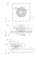
図3は、第1実施形態のモールドMの断面図である。モールドMは、第1部分40と第2部分41とを含む。第1部分40は、パターンMpが設けられたパターン部40a(メサ部)とパターン部40aを取り囲む周辺部40b(オフメサ部)とを含む第1面4a1と、第1面4a1の反対側の第2面4a2とを有する。第2部分41は、第1部分40を取り囲み、かつ第1部分40よりモールドMの厚み(Z方向)が厚くなるように構成される。また、パターン部40a(メサ部)は、基板Wに向かって突出した構成(凸型)となっている。パターン部40aにはパターンMpを囲むようにスクライブラインが配置されていることある。モールドMの位置合わせに用いられるモールド側マーク10はスクライブライン上に形成されていることが多い。本実施形態では、モールドのパターン部はパターンMpとスクライブラインが含まれているものとする。このように構成されたモールドMには、第1部分40の第2面4a2と第2部分41の内側の第3面4a3とによって凹部4c(キャビティ、コアアウト)が形成される。このようにモールドMに凹部4cを形成することで、凹部4c内の圧力(例えば気圧)を変えたときにモールドMの第1部分40(第1面4a1)が変形しやすくなっている。
(About mold)
FIG. 3 is a sectional view of the mold M according to the first embodiment. The mold M includes a
(インプリント処理について)
次に、図4を用いてインプリント装置100によるインプリント処理について説明する。インプリント処理が開始されると、第1実施形態のモールドMがインプリント装置100に搬入され、モールド保持部6によって保持される(S401)。このとき、図2に示す状態で、アライメント光学系2の受光ユニット2aが、モールド側マーク10と基準マーク12を検出し、基板ステージ5に対するモールドMの位置合わせを行う(S401)。その際、ステージ基準プレート7の基準マーク12は、モールドMを透過して検出するが、モールドのパターンがあると基準マーク12が検出しにくい。そのため、基準マーク12は、パターンやマークが形成されていないオフメサ部(図3の40b)を透過する位置に形成されている。
(About imprint processing)
Next, the imprint process by the
次に、基板搬送部(不図示)により基板Wがインプリント装置100に搬入され、基板Wは基板ステージ5に保持される(S402)。基板Wに形成されたショット領域(パターン形成領域)がモールドMのパターンMpの直下に配置される(位置する)ように、基板ステージ5を移動させる(S403)。ここでは、基板Wの全面にインプリント材Rを予め塗布しておき、インプリント材Rが全面に塗布された基板Wにおける複数のショット領域の各々に対してインプリント処理を順次行っていく。第1実施形態では、基板Wの全面に予めインプリント材Rが供給されている場合について説明しているが、インプリント装置100内でショット領域にインプリント材Rを供給する場合は、S402とS403の間に供給工程(塗布工程)が含まれていてもよい。
Next, the substrate W is carried into the
次に、モールド保持部6の駆動機構を駆動させ、基板W上のインプリント材RにモールドMを接触させる(S404・押印工程)。モールドMに接触したインプリント材Rは、モールドMに形成されたパターンMpの凹凸パターンに沿って流動する(S405・充填工程)。モールドMとインプリント材Rが接触した状態で、モールド側マーク10および基板側マーク11をアライメント光学系2が検出する。アライメント光学系2の検出結果に基づいて基板ステージ5を駆動させることにより、基板WとモールドMの位置合わせを行う(S406)。また、アライメント光学系2の検出結果に基づいて、モールド変形機構によりモールドM(ショット領域)を変形させる補正や、基板Wに熱を加えることによりショット領域を変形させる補正を実施してもよい(S407)。
Next, the drive mechanism of the mold holding unit 6 is driven to bring the mold M into contact with the imprint material R on the substrate W (S404/imprinting step). The imprint material R in contact with the mold M flows along the uneven pattern of the pattern Mp formed on the mold M (S405, filling step). The alignment
モールドMと基板Wの位置合わせがなされた段階で、照明系1はモールドMの背面(上面)からインプリント材Rに紫外光を照射することで、インプリント材Rを硬化させる(S408・硬化工程)。インプリント材Rを硬化させた後、モールド保持部6の駆動機構を駆動させ、モールドMを硬化したインプリント材Rから引き離す(S409・離型工程)。モールドMをインプリント材Rから引き離すことにより、基板Wのショット領域上にインプリント材Rのパターンが形成される。つまり、モールドMに形成された凹凸形状のパターンMpが基板W上に転写される。さらに、第1実施形態のインプリント処理は、S404の押印工程からS409の離型工程の間の少なくとも一部において、観察光学系3はパターン部を観察することができる(S410)。観察光学系3の検出視野内において、インプリント処理の各工程で異常が発生していないかを観察することができる。
When the mold M and the substrate W are aligned, the
第1実施形態に示すインプリント処理は、基板Wの全面にインプリント材Rを予め塗布しておき、インプリント材Rが全面に塗布された基板Wにおける複数のショット領域の各々に対してインプリント処理を順次行っていく。 In the imprint process shown in the first embodiment, the imprint material R is applied on the entire surface of the substrate W in advance, and the imprint material R is imprinted on each of a plurality of shot regions on the substrate W applied on the entire surface. The printing process is performed sequentially.
しかし、図5(a)に示すように、パターンMpをインプリント材Rに接触させた状態で、ショット領域50aに硬化光(図中灰色部)を照射すると、基板WやモールドMの表面で硬化光が反射する。硬化光の反射により、モールドMやインプリント装置内の共通の光学部材21で再び反射し(図中点線矢印)、基板W上のショット領域50aの周辺領域50bに反射した光(フレア光ともいう)が到達してしまう恐れがある。
However, as shown in FIG. 5A, when the
その結果、図5(b)に示すように、ショット領域50aに供給されたインプリント材Rだけでなく、ショット領域50aの周辺領域50bや隣接ショット領域50cに塗布されたインプリント材Rも硬化してしまう恐れがある。例えば、図5(b)に示すように、ショット領域50aに供給されたインプリント材R1が硬化するのに加えて、周辺領域50bや隣接ショット領域50cに塗布されたインプリント材R2が半硬化状態であることを示している。ここで、周辺領域50bとは、ショット領域とショット領域の間の領域であり、例えばスクライブラインとすることができる。このように周辺領域50bや隣接ショット領域50cにおけるインプリント材Rが硬化もしくは半硬化状態になると、この後にインプリントを行う隣接ショット領域50cにおいて、インプリント処理が正常に行うことができなくなる。
As a result, as shown in FIG. 5B, not only the imprint material R supplied to the
(実施例1)
そこで、第1実施形態におけるモールドMの凹部には、図3に示すように、周辺部40b(オフメサ部)のうち基板Wに対向する面の反対側の面に遮光部9が設けられている。遮光部9は、モールドMに入射した硬化光がパターンMpのパターン部40aを透過するように、パターン部40aの周囲に設けられている。ただし、遮光部9が、例えばクロムなどの金属膜で構成されると、硬化光(紫外光)のみならず、アライメント光や観察光(可視〜赤外光)も遮光されてしまうため好ましくない。
(Example 1)
Therefore, in the concave portion of the mold M in the first embodiment, as shown in FIG. 3, the
そこで、本発明の遮光部9は、硬化光は遮光するが、観察光またはアライメント光は透過する特性を有している。遮光部9にこの特性を有することで、周辺領域50bや隣接ショット領域50cに硬化光が照明されないように遮光しつつ、観察光により周辺領域50bや隣接ショット領域50cを観察することができる。また、硬化光を遮光しつつ、インプリント装置100の基準マーク12や周辺領域50bや隣接ショット領域50cに配置されたマーク(アライメントマーク)を検出することができる。このように、第1実施形態の遮光部9は遮光膜9aからなり、紫外光を遮光し、可視から赤外光の波長帯域の光は透過する特性を有する材料であることが望ましい。遮光膜9aは、例えば、誘電体多層膜(Al2O3、SiO、MgF2)や、CrN、TaNなどの金属窒化物、Cr2O3、TiOなどの金属酸化物などの材料で構成されうる。
Therefore, the light-shielding
図6は、遮光膜9aをモールドMに設けた場合の分光透過率特性を示したものである。図6は、横軸が波長を示し縦軸が透過率を示している。遮光膜9aとして、モールドMに、膜厚210nmのCrNを設けた場合、膜厚1000nmのCr2O3を設けた場合、膜厚120nmのTaNを設けた場合を示している。本発明で必要とされる透過率特性は、紫外領域の透過率をなるべく小さく(好ましくは波長400nm以下で1%以下と)し、可視から赤外領域の透過率をなるべく大きく(好ましくは波長帯域500〜800nmで10%以上と)する。遮光膜9aとするそれぞれの材料について膜厚を比較すると、必要な膜厚が異なることを示している。遮光膜9aの特性として、例えば、波長帯域380nm以下の光の透過率を0%以上、1%以下とし、波長帯域500〜800nmの光の透過率を10%以上、100%以下としている。
FIG. 6 shows the spectral transmittance characteristics when the
遮光膜9aとして利用できる材料は図6のように、それぞれの材料について分光透過率特性を求めることで、判断することができる。また、透過率は各材料の消衰係数κ(消光係数)と結びつきが強く、遮光膜9aとして利用できる材料を消衰係数κによって求めることも可能である。図10は、図6に示した各材料(CrN、Cr2O3、TaN)の消衰係数(消光係数)κを縦軸に示したもので、横軸は波長である。
The material that can be used as the light-shielding
CrNの消衰係数κは、硬化光の波長帯域(例えば300〜400nm)で0.67以上、アライメント光の波長帯域(例えば500〜800nm)で0.21以下であり、硬化光は透過しにくく、アライメント光や観察光は透過しやすい特性となっている。同様に、Cr2O3の消衰係数κは、300〜400nmで0.10以上、500〜800nmで0.02以下である。同様に、TaNの消衰係数κは、300〜400nmで1.10以上、500〜800nmで0.61以下である。いずれも、硬化光は透過しにくく、アライメント光や観察光は透過しやすい特性となっている。 The extinction coefficient κ of CrN is 0.67 or more in the wavelength band of curing light (for example, 300 to 400 nm) and 0.21 or less in the wavelength band of alignment light (for example, 500 to 800 nm), which makes it difficult for the curing light to pass through. The alignment light and the observation light are easily transmitted. Similarly, the extinction coefficient κ of Cr 2 O 3 is 0.10 or more at 300 to 400 nm and 0.02 or less at 500 to 800 nm. Similarly, the extinction coefficient κ of TaN is 1.10 or more at 300 to 400 nm and 0.61 or less at 500 to 800 nm. In both cases, the curing light is difficult to transmit, and the alignment light and the observation light are easily transmitted.
ここで、300〜380nmの波長帯域の消衰係数κを[κa]、500〜800nmの波長帯域の消衰係数κを[κb]とし、[κa]/[κb]との関係をまとめると、表1のようになる。 Here, the extinction coefficient κ in the wavelength band of 300 to 380 nm is [κa], the extinction coefficient κ in the wavelength band of 500 to 800 nm is [κb], and the relation with [κa]/[κb] is summarized as follows. It becomes like Table 1.

以上から、遮光部9の材料は、[κa]が0.1以上(好ましくは、0.5以上)で、[κa]/[κb]が1.8以上(好ましくは、3.0以上)となる条件であることが望ましい。
From the above, the material of the
図7は、遮光部9が設けられた第1実施形態の実施例1のモールドMを示す図である。モールドMは、インプリント装置100において用いられる。図7に示すようにモールドMは、モールドMの第2面4a2においてパターン部40aを囲むように遮光部9(遮光膜9a)が設けられている。図7(a)は、モールドMをZ方向から見たときの図であり、二点破線は照明系1の照明視野(照明系1の硬化光1aが照明する領域)を示す。また、図中の点線は、硬化光1aのフレア光が到達する領域1bを示す。
FIG. 7 is a diagram showing the mold M of Example 1 of the first embodiment in which the
図7(b)は、モールドMと基板W上のインプリント材Rとを接触させ、インプリント材RにモールドMを介して硬化光1aと観察光3a(検出光)を照射している様子を示す図である。図7の遮光膜9aは、硬化光がパターンMpを透過するように構成されている。そして、遮光膜9aにより周辺領域50bや隣接ショット領域50cが照明されないように硬化光1a(フレア光を含む)を遮光している。一方、観察光3aは遮光膜9aを透過するため、パターン部40aの周辺部である周辺領域50bや隣接ショット領域50cの観察が可能となっている。
In FIG. 7B, the mold M and the imprint material R on the substrate W are brought into contact with each other, and the imprint material R is irradiated with the curing light 1a and the observation light 3a (detection light) through the mold M. FIG. The
図7(c)は、モールドMとステージ基準プレート7の位置合わせ工程を示す図である。基板ステージ5に設けられたステージ基準プレート7の基準マーク12は、モールドMにおけるパターンが形成されていない周辺部40b(オフメサ部)の下になるように配置されている。そして、アライメント光学系2は、アライメント光2b(検出光)を照明することによって、モールドMのパターンMpが形成されたパターン部40aに形成されたモールド側マーク10とステージ基準プレート7の基準マーク12を検出する。そして、マークの検出結果に基づいてモールドMとステージ基準プレート7(基準マーク12)位置合わせを行う。このようにモールドMは、遮光膜9aにより周辺領域50bや隣接ショット領域50cが照明されないように硬化光1a(フレア光を含む)を遮光している。一方、アライメント光2bや観察光3aは遮光膜9aを透過するため、周辺領域50bに形成されたインプリント装置の基準マーク12を検出したり、隣接ショット領域50cの状態を観察したりすることができる。
FIG. 7C is a diagram showing a step of aligning the mold M and the
(実施例2)
図8は、遮光部9が設けられた第1実施形態の実施例2のモールドMを示す図である。モールドMは、インプリント装置100において用いられる。図8(a)に示すようにモールドMは、モールドMの第1面4a1においてパターンMpが形成されたパターン部40aを囲むように遮光部9(遮光膜9a)が設けられている。実施例1のモールドは、モールドMの第2面4a2にパターン部40aを取り囲むように遮光部9(遮光膜9a)が設けられている場合について説明した。図8(a)のように、遮光部9はモールドMの第2面4a2に限られず、モールドMの第1面4a1に設けても良い。さらに、遮光膜9aは、図8(b)に示すように、モールドMの第1面4a1および第2面4a2の周辺部40b(オフメサ部)に対応する領域に形成されてもよい。実施例1と同様に、実施例2の遮光膜9aは、硬化光は遮光するが、観察光またはアライメント光は透過する特性を有している。
(Example 2)
FIG. 8 is a diagram showing a mold M of Example 2 of the first embodiment in which the
図8に示したモールドMのように遮光膜9aを形成することにより、ショット領域の周辺に硬化光が照射されることを低減することができる。モールドMの第1面4a1に遮光膜9aを設けることは、より基板の表面に近いに遮光部9を配置することができる。そのため、モールドMの第2面4a2に斜めから入射した硬化光を遮光することができ、斜めから入射した光によって周辺領域50bが照明されないようにすることができる。実施例2も同様に、周辺領域50bに照射される硬化光を遮光するともに、アライメント光2bを透過させることにより、ショット領域50aの周辺部に設けられたインプリント装置の基準マークを検出したり、周辺部の様子を観察したりすることができる。
By forming the light-shielding
(第2実施形態)
次に、第2実施形態のインプリント装置について説明する。第1実施形態では、遮光部9は、モールドMの表面に設けられた遮光膜9aとして構成されているが、第2実施形態では、遮光部9は、モールドMの凹部4cに取り外しできるように構成された遮光部材9bとして構成される。
(Second embodiment)
Next, the imprint apparatus of the second embodiment will be described. In the first embodiment, the light-shielding
以下、遮光部9として構成された遮光部材9bについて説明する。ここで、第2実施形態のインプリント装置は、第1実施形態のインプリント装置100と比べて、遮光部9以外の装置構成が同じであるため、ここでは遮光部9以外の装置構成についての説明を省略する。
Hereinafter, the light shielding member 9b configured as the
図9は、第2実施形態のインプリント装置において用いられるモールドMと遮光部材9bとを示す図である。図9(a)は、モールドMと遮光部材9bをZ方向から見たときの図を示す。図9(b)は、図9(a)における断面A‐A´を示した図であり、モールドMと遮光部材9bの断面図である。遮光部材9bは、上述したように、モールドMの凹部4cから取り外しできるように構成されている。
FIG. 9 is a diagram showing the mold M and the light shielding member 9b used in the imprint apparatus of the second embodiment. FIG. 9A shows a view of the mold M and the light shielding member 9b when viewed from the Z direction. 9B is a view showing a cross section AA′ in FIG. 9A and is a cross sectional view of the mold M and the light shielding member 9b. As described above, the light shielding member 9b is configured to be removable from the
遮光部材9bには、モールドMの凹部4cに設けられたピン4eに対応する位置に貫通穴17が形成されている。そして、遮光部材9bは、その貫通穴17にピン4eを貫通させることによってモールドMに固定されており、モールドMに対する、基板Wの面と平行な面方向(XY方向)に沿ったずれ量を許容範囲に収めることができる。このように遮光部材9bを構成する場合、例えば、モールドMに対するXY方向のずれ量を、±5μmの許容範囲に収まることができる。
Through holes 17 are formed in the light shielding member 9b at positions corresponding to the
遮光部材9bは、インプリント材を硬化させる硬化光は遮光するが、観察光およびアライメント光を透過させる特性を有している。遮光部材9bは、硬化光が通過する開口18が設けられている。開口18を通過した硬化光はパターンMp(パターン部40a)を照明することができる。このような遮光部材9bを構成することにより、インプリント装置100は、パターン部に形成されたパターンMpを転写すべきショット領域50aに硬化光を照射しつつ、周辺領域50bに硬化光が照射されることを低減することができる。更に、周辺領域50bや隣接ショット領域50cにおけるインプリント工程の観察機能や、パターン部40aの領域外に形成されたマークの検出が可能となる。
The light blocking member 9b has a property of blocking the curing light for curing the imprint material but transmitting the observation light and the alignment light. The light blocking member 9b is provided with an
ここで、遮光部材9bは、石英など観察光やアライメント光、硬化光に対して透明な部材を用いて、開口18以外の領域に遮光膜が設けられている。遮光膜は、硬化光として紫外光を遮光し、観察光やアライメント光として可視光や赤外光を透過させる特性を有する材料であることが望ましい。例えば、石英に誘電体多層膜や、CrNなどの金属窒化物、Cr2O3、TiOなどの金属酸化物で構成されうる。材料は、これらに限られるものではなく、インプリント材Rを硬化させる硬化光を遮光しつつ、アライメント光や観察光を透過することができれば良い。
Here, as the light blocking member 9b, a member such as quartz that is transparent to the observation light, the alignment light, and the curing light is used, and the light blocking film is provided in the region other than the
第2実施形態のインプリント装置では、遮光部9として、モールドMの凹部4cから取り外しできるように構成された遮光部材9bが用いられる。このように構成された遮光部材9bを遮光部9として用いることにより、モールドMを洗浄する際、モールドMから遮光部材9bを取り外すことができる。そのため、モールドMの洗浄する際に遮光部9も剥がれてしまう恐れを低減することができる。
In the imprint apparatus of the second embodiment, as the
ここで、第1実施形態において遮光部9として用いた遮光膜9aと、第2実施形態において遮光部9として用いた遮光部材9bを併用してもよい。
Here, the
(その他)
上述の何れの実施形態も、基板Wの全面にインプリント材Rが塗布されている基板を用いたが、それに限られず、インプリント材Rが塗布されていない基板Wをインプリント装置100に搬入しても良い。インプリント装置100に設けられた供給部(ディスペンサ)によって、インプリント材Rを所望の数のショット領域上に塗布してもよい。
(Other)
In all of the above-described embodiments, the substrate in which the imprint material R is applied to the entire surface of the substrate W is used. You may do it. The imprint material R may be applied onto a desired number of shot areas by a supply unit (dispenser) provided in the
本発明は隣接ショットに積極的にインプリント材が供給されない場合であっても、例えば、パターンを形成するショット領域からはみ出したインプリント材が存在することがある。そのため、このような場合にも、本発明のモールドMを用いることによって周辺領域上のインプリント材を硬化させることなく、ショット領域上にパターンを形成することができる。 In the present invention, even when the imprint material is not positively supplied to the adjacent shot, for example, the imprint material may be present outside the shot area where the pattern is formed. Therefore, even in such a case, by using the mold M of the present invention, a pattern can be formed on the shot area without curing the imprint material on the peripheral area.
(物品製造方法)
インプリント装置を用いて形成した硬化物のパターンは、各種物品の少なくとも一部に恒久的に、或いは各種物品を製造する際に一時的に、用いられる。物品とは、電気回路素子、光学素子、MEMS、記録素子、センサ、或いは、型等である。電気回路素子としては、DRAM、SRAM、フラッシュメモリ、MRAMのような、揮発性或いは不揮発性の半導体メモリや、LSI、CCD、イメージセンサ、FPGAのような半導体素子等が挙げられる。型としては、インプリント用のモールド等が挙げられる。
(Product manufacturing method)
The pattern of the cured product formed by using the imprint apparatus is used permanently on at least a part of various articles or temporarily when manufacturing various articles. The article is an electric circuit element, an optical element, a MEMS, a recording element, a sensor, a mold, or the like. Examples of the electric circuit element include volatile or non-volatile semiconductor memory such as DRAM, SRAM, flash memory, and MRAM, and semiconductor elements such as LSI, CCD, image sensor, and FPGA. Examples of the mold include a mold for imprint and the like.
硬化物のパターンは、上記物品の少なくとも一部の構成部材として、そのまま用いられるか、或いは、レジストマスクとして一時的に用いられる。基板の加工工程においてエッチング又はイオン注入等が行われた後、レジストマスクは除去される。 The pattern of the cured product is used as it is as a constituent member of at least a part of the above article, or is temporarily used as a resist mask. The resist mask is removed after etching or ion implantation is performed in the substrate processing step.
次に、物品の具体的な製造方法について説明する。図11(a)に示すように、絶縁体等の被加工材2zが表面に形成されたシリコンウエハ等の基板1zを用意し、続いて、インクジェット法等により、被加工材2zの表面にインプリント材3zを付与する。ここでは、複数の液滴状になったインプリント材3zが基板上に付与された様子を示している。
Next, a specific method for manufacturing the article will be described. As shown in FIG. 11A, a
図11(b)に示すように、インプリント用の型4zを、その凹凸パターンが形成された側を基板1z上のインプリント材3zに向け、対向させる。図11(c)に示すように、インプリント材3zが付与された基板1zと型4zとを接触させ、圧力を加える。インプリント材3zは型4zと被加工材2zとの隙間に充填される。この状態で硬化用のエネルギーとして光を。型4zを透して照射すると、インプリント材3zは硬化する。
As shown in FIG. 11B, the imprinting mold 4z is opposed to the imprinting material 3z on the
図11(d)に示すように、インプリント材3zを硬化させた後、型4zと基板1zを引き離すと、基板1z上にインプリント材3zの硬化物のパターンが形成される。この硬化物のパターンは、型の凹部が硬化物の凸部に、型の凸部が硬化物の凹部に対応した形状になっており、即ち、インプリント材3zに型4zの凹凸パターンが転写されたことになる。
As shown in FIG. 11D, when the imprint material 3z is cured and then the mold 4z and the
図11(e)に示すように、硬化物のパターンを耐エッチングマスクとしてエッチングを行うと、被加工材2zの表面のうち、硬化物が無いか或いは薄く残存した部分が除去され、溝5zとなる。図11(f)に示すように、硬化物のパターンを除去すると、被加工材2zの表面に溝5zが形成された物品を得ることができる。ここでは硬化物のパターンを除去したが、加工後も除去せずに、例えば、半導体素子等に含まれる層間絶縁用の膜、つまり、物品の構成部材として利用してもよい。
As shown in FIG. 11E, when etching is performed using the pattern of the cured product as an etching resistant mask, the portion of the surface of the workpiece 2z where the cured product is absent or remains thin is removed to form the
以上、本発明の好ましい実施形態について説明したが、本発明は、これらの実施形態に限定されず、その要旨の範囲内で種々の変形および変更が可能である。 Although the preferred embodiments of the present invention have been described above, the present invention is not limited to these embodiments, and various modifications and changes can be made within the scope of the gist thereof.
1 照明系
2 アライメント光学系
3 観察光学系
5 基板ステージ
6 モールド保持部
7 ステージ基準プレート
M モールド
W 基板
R インプリント材
9 遮光部
100 インプリント装置
1
Claims (20)
前記インプリント材を硬化させる硬化光が透過するパターン部と、
前記パターン部を取り囲む周辺部と、を含み、
前記周辺部に、前記インプリント材を硬化させる硬化光を減光し、且つ前記モールドを介して被検物を検出するための検出光を透過させる膜が設けられており、
前記パターン部は、前記モールドと前記基板との位置合わせのために用いられるマークを含み、前記パターン部には、前記膜が設けられていないことを特徴とするモールド。 A mold used to form a pattern of imprint material on a substrate ,
A pattern portion curing light to cure the imprint material passes,
A peripheral portion surrounding the pattern portion,
The peripheral portion is provided with a film that attenuates curing light for curing the imprint material and that transmits detection light for detecting an object to be inspected through the mold ,
The pattern part includes a mark used for alignment between the mold and the substrate, and the pattern part is not provided with the film .
インプリント材を硬化させる硬化光が透過するパターン部と、A pattern portion that cure light for curing the imprint material is transmitted,
前記パターン部を取り囲む周辺部と、を含み、A peripheral portion surrounding the pattern portion,
前記周辺部に、前記インプリント材を硬化させる硬化光を減光し、且つ前記モールドを介して被検物を検出するための検出光を透過させる膜が設けられており、The peripheral portion is provided with a film that attenuates curing light for curing the imprint material and that transmits detection light for detecting an object to be inspected through the mold,
前記膜は、前記硬化光の波長帯域の透過率が0%以上、1%以下であり、前記検出光の波長帯域の透過率が10%以上、100%以下であることを特徴とするモールド。The mold has a transmittance of 0% or more and 1% or less in the wavelength band of the curing light, and a transmittance of 10% or more and 100% or less in the wavelength band of the detection light of the film.
インプリント材を硬化させる硬化光が透過するパターン部と、A pattern portion that cure light for curing the imprint material is transmitted,
前記パターン部を取り囲む周辺部と、を含み、A peripheral portion surrounding the pattern portion,
前記周辺部に、前記インプリント材を硬化させる硬化光を減光し、且つ前記モールドを介して被検物を検出するための検出光を透過させる膜が設けられており、The peripheral portion is provided with a film that attenuates curing light for curing the imprint material and that transmits detection light for detecting an object to be inspected through the mold,
前記膜は、500〜800nmの波長帯域の波長の消衰係数に対する300〜380nmの波長帯域の波長の消衰係数の比が1.8以上であることを特徴とするモールド。The said film|membrane has a ratio of the extinction coefficient of the wavelength of a 300-380 nm wavelength band with respect to the extinction coefficient of the wavelength of a 500-800 nm wavelength band is 1.8 or more, The mold characterized by the above-mentioned.
前記モールドと前記基板を位置合わせする工程と、
前記モールドを前記インプリント材に接触させ、前記インプリント材を硬化させる工程と、を含み、
前記パターン部には前記膜が設けられておらず、モールドと前記基板の位置合わせにおいて、前記パターン部に設けられたマークが検出されることを特徴とするインプリント方法。 A mold including a pattern portion that transmits curing light for curing an imprint material and a peripheral portion surrounding the pattern portion , wherein the peripheral portion dims the curing light for curing the imprint material, and the mold is An imprinting method for forming a pattern of an imprinting material on a substrate using a mold provided with a film that transmits detection light for detecting an object to be inspected ,
Aligning the mold and the substrate,
Contacting the mold with the imprint material, and curing the imprint material,
The imprint method , wherein the pattern portion is not provided with the film, and a mark provided on the pattern portion is detected during alignment between the mold and the substrate .
前記モールドと前記基板を位置合わせする工程と、Aligning the mold and the substrate,
前記モールドを前記インプリント材に接触させ、前記インプリント材を硬化させる工程と、を含み、Contacting the mold with the imprint material, and curing the imprint material,
前記膜は、前記インプリント材を硬化させる硬化光を減光し、且つ前記モールドを介して被検物を検出するための検出光を透過させ、The film attenuates curing light for curing the imprint material, and transmits detection light for detecting an object to be inspected through the mold,
前記膜は、前記硬化光の波長帯域の透過率が0%以上、1%以下であり、前記検出光の波長帯域の透過率が10%以上、100%以下であることを特徴とするインプリント方法。The film has a transmittance in the wavelength band of the curing light of 0% or more and 1% or less, and a transmittance in the wavelength band of the detection light of 10% or more and 100% or less. Method.
前記モールドと前記基板を位置合わせする工程と、Aligning the mold and the substrate,
前記モールドを前記インプリント材に接触させ、前記インプリント材を硬化させる工程と、を含み、Contacting the mold with the imprint material, and curing the imprint material,
前記膜は、前記インプリント材を硬化させる硬化光を減光し、且つ前記モールドを介して被検物を検出するための検出光を透過させ、The film attenuates curing light for curing the imprint material, and transmits detection light for detecting an object to be inspected through the mold,
前記膜は、500〜800nmの波長帯域の波長の消衰係数に対する300〜380nmの波長帯域の波長の消衰係数の比が1.8以上であることを特徴とするインプリント方法。The imprint method according to claim 1, wherein the film has a ratio of an extinction coefficient of a wavelength in the wavelength band of 300 to 380 nm to an extinction coefficient of a wavelength in the wavelength band of 500 to 800 nm of 1.8 or more.
前記工程で前記パターンが形成された前記基板を加工する工程と、
を含むことを特徴とする物品製造方法。 A step of forming a pattern of an imprint material on a substrate using the imprint method according to any one of claims 16 to 18 ,
A step of processing the substrate on which the pattern is formed in the step,
A method for manufacturing an article, comprising:
Priority Applications (6)
| Application Number | Priority Date | Filing Date | Title |
|---|---|---|---|
| JP2016130918A JP6748496B2 (en) | 2016-06-30 | 2016-06-30 | Mold, imprint method, imprint apparatus, and article manufacturing method |
| SG10201704389PA SG10201704389PA (en) | 2016-06-30 | 2017-05-30 | Mold, imprinting method, imprint apparatus, and method for manufacturing a semiconductor article |
| TW106119300A TWI643019B (en) | 2016-06-30 | 2017-06-09 | Mold, imprinting method, imprint apparatus, and method for manufacturing a semiconductor article |
| US15/630,600 US20180004091A1 (en) | 2016-06-30 | 2017-06-22 | Mold, imprinting method, imprint apparatus, and method for manufacturing a semiconductor article |
| KR1020170078955A KR102280003B1 (en) | 2016-06-30 | 2017-06-22 | Mold, imprinting method, imprint apparatus, and method for manufacturing a semiconductor article |
| CN201710506145.2A CN107561855A (en) | 2016-06-30 | 2017-06-28 | Mould, method for stamping, imprinting apparatus and the method for manufacturing semiconductor article |
Applications Claiming Priority (1)
| Application Number | Priority Date | Filing Date | Title |
|---|---|---|---|
| JP2016130918A JP6748496B2 (en) | 2016-06-30 | 2016-06-30 | Mold, imprint method, imprint apparatus, and article manufacturing method |
Publications (3)
| Publication Number | Publication Date |
|---|---|
| JP2018006553A JP2018006553A (en) | 2018-01-11 |
| JP2018006553A5 JP2018006553A5 (en) | 2019-07-18 |
| JP6748496B2 true JP6748496B2 (en) | 2020-09-02 |
Family
ID=60806962
Family Applications (1)
| Application Number | Title | Priority Date | Filing Date |
|---|---|---|---|
| JP2016130918A Active JP6748496B2 (en) | 2016-06-30 | 2016-06-30 | Mold, imprint method, imprint apparatus, and article manufacturing method |
Country Status (6)
| Country | Link |
|---|---|
| US (1) | US20180004091A1 (en) |
| JP (1) | JP6748496B2 (en) |
| KR (1) | KR102280003B1 (en) |
| CN (1) | CN107561855A (en) |
| SG (1) | SG10201704389PA (en) |
| TW (1) | TWI643019B (en) |
Families Citing this family (9)
| Publication number | Priority date | Publication date | Assignee | Title |
|---|---|---|---|---|
| JP6815894B2 (en) * | 2017-02-27 | 2021-01-20 | 株式会社ディスコ | How to use the electrostatic chuck table |
| CN108445711A (en) * | 2018-03-13 | 2018-08-24 | 京东方科技集团股份有限公司 | A kind of display base plate and preparation method thereof, display device |
| US11281095B2 (en) | 2018-12-05 | 2022-03-22 | Canon Kabushiki Kaisha | Frame curing template and system and method of using the frame curing template |
| JP2021027107A (en) | 2019-08-01 | 2021-02-22 | キヤノン株式会社 | Imprint apparatus, imprint method, and article manufacturing method |
| JP7346268B2 (en) | 2019-12-05 | 2023-09-19 | キヤノン株式会社 | Imprint templates, imprint methods using templates |
| JP7465146B2 (en) * | 2020-05-12 | 2024-04-10 | キヤノン株式会社 | Imprinting method, imprinting apparatus, evaluation method and article manufacturing method |
| CN113885295B (en) * | 2020-07-01 | 2024-03-08 | 吉佳蓝科技股份有限公司 | Replica molding device for nanoimprint |
| US11747731B2 (en) | 2020-11-20 | 2023-09-05 | Canon Kabishiki Kaisha | Curing a shaped film using multiple images of a spatial light modulator |
| JP2022182118A (en) | 2021-05-27 | 2022-12-08 | キヤノン株式会社 | Mold, imprint device, and method for manufacturing article |
Family Cites Families (15)
| Publication number | Priority date | Publication date | Assignee | Title |
|---|---|---|---|---|
| JP3410089B2 (en) * | 1991-11-13 | 2003-05-26 | 株式会社東芝 | Exposure mask manufacturing method and exposure method |
| US9573319B2 (en) * | 2007-02-06 | 2017-02-21 | Canon Kabushiki Kaisha | Imprinting method and process for producing a member in which a mold contacts a pattern forming layer |
| JP5182470B2 (en) * | 2007-07-17 | 2013-04-17 | 大日本印刷株式会社 | Imprint mold |
| JP4799575B2 (en) * | 2008-03-06 | 2011-10-26 | 株式会社東芝 | Imprint method |
| JP5257225B2 (en) * | 2009-04-28 | 2013-08-07 | 大日本印刷株式会社 | Nanoimprint mold and manufacturing method thereof |
| JP5531702B2 (en) * | 2010-03-23 | 2014-06-25 | 旭硝子株式会社 | Glass substrate with light shielding film and liquid crystal display device |
| JP6029494B2 (en) * | 2012-03-12 | 2016-11-24 | キヤノン株式会社 | Imprint method, imprint apparatus, and article manufacturing method using the same |
| JP6173354B2 (en) * | 2013-01-24 | 2017-08-02 | 綜研化学株式会社 | Light transmission type imprint mold, large area mold manufacturing method |
| JP6368075B2 (en) * | 2013-06-26 | 2018-08-01 | キヤノン株式会社 | mold |
| JP5909210B2 (en) * | 2013-07-11 | 2016-04-26 | キヤノン株式会社 | Imprint apparatus and article manufacturing method |
| JP6097704B2 (en) * | 2014-01-06 | 2017-03-15 | キヤノン株式会社 | Imprint apparatus, imprint method, and article manufacturing method |
| JP2015144193A (en) * | 2014-01-31 | 2015-08-06 | 株式会社東芝 | Imprint method, template and imprint device |
| TWI662591B (en) * | 2014-07-08 | 2019-06-11 | 日商綜研化學股份有限公司 | Step-and-repeat embossing method using step-and-repeat embossing mold, and manufacturing method of step-and-repeat embossing mold |
| JP5900589B2 (en) * | 2014-12-12 | 2016-04-06 | 大日本印刷株式会社 | Imprint mold, alignment method, imprint method, and imprint apparatus |
| JP2016028442A (en) * | 2015-10-08 | 2016-02-25 | 大日本印刷株式会社 | Template |
-
2016
- 2016-06-30 JP JP2016130918A patent/JP6748496B2/en active Active
-
2017
- 2017-05-30 SG SG10201704389PA patent/SG10201704389PA/en unknown
- 2017-06-09 TW TW106119300A patent/TWI643019B/en active
- 2017-06-22 KR KR1020170078955A patent/KR102280003B1/en active IP Right Grant
- 2017-06-22 US US15/630,600 patent/US20180004091A1/en not_active Abandoned
- 2017-06-28 CN CN201710506145.2A patent/CN107561855A/en active Pending
Also Published As
| Publication number | Publication date |
|---|---|
| JP2018006553A (en) | 2018-01-11 |
| US20180004091A1 (en) | 2018-01-04 |
| KR102280003B1 (en) | 2021-07-21 |
| CN107561855A (en) | 2018-01-09 |
| TW201802578A (en) | 2018-01-16 |
| SG10201704389PA (en) | 2018-01-30 |
| KR20180003437A (en) | 2018-01-09 |
| TWI643019B (en) | 2018-12-01 |
Similar Documents
| Publication | Publication Date | Title |
|---|---|---|
| JP6748496B2 (en) | Mold, imprint method, imprint apparatus, and article manufacturing method | |
| TWI720301B (en) | Imprint apparatus and method of manufacturing article | |
| TWI668734B (en) | Imprint apparatus, imprinting method, and method for manufacturing article | |
| KR20140119800A (en) | Imprint method, imprint apparatus, and article manufacturing method using the same | |
| US11709421B2 (en) | Imprint apparatus | |
| KR102317410B1 (en) | Imprint apparatus, imprint method, method of determining layout pattern of imprint material, and article manufacturing method | |
| KR20180118043A (en) | Imprint apparatus, method of generating control data, and article manufacturing method | |
| US10386737B2 (en) | Imprint apparatus and method for producing article | |
| JP2021082672A (en) | Imprint device, imprint method, and article manufacturing method | |
| WO2018088049A1 (en) | Imprint device, imprint method, and article manufacturing method | |
| US20210132492A1 (en) | Imprint apparatus, imprint method, and method for manufacturing article | |
| US20210187797A1 (en) | Imprint apparatus, imprint method, and method of manufacturing article | |
| KR20210065854A (en) | Imprinting apparatus, imprinting method, method for producing article, substrate, and mold | |
| JP2020161634A (en) | Imprint device, imprint method, and article manufacturing method | |
| JP2018113418A (en) | Imprint device, and article manufacturing method | |
| JP7383450B2 (en) | Imprint equipment, imprint method, and article manufacturing method | |
| JP7171383B2 (en) | IMPRINT APPARATUS AND ARTICLE MANUFACTURING METHOD | |
| US20230415403A1 (en) | Imprint system, substrate, imprint method, replica mold manufacturing method, and article manufacturing method | |
| US20230294351A1 (en) | Object alignment method, imprint method, article manufacturing method, detection apparatus, imprint apparatus, mold, and substrate | |
| KR102211390B1 (en) | Imprint device and article manufacturing method | |
| JP2022038752A (en) | Substrate processing method, substrate holding device, molding device, and manufacturing method for article | |
| JP2021068766A (en) | Liquid dispensing device, molding device, and manufacturing method of article | |
| JP2018182303A (en) | Semiconductor substrate, pattern forming method and article manufacturing method | |
| JP2019021875A (en) | Imprint method, imprint device, and manufacturing method of material | |
| JP2020038164A (en) | Position detection device, position detection method, mold, imprint device, and method for manufacturing article |
Legal Events
| Date | Code | Title | Description |
|---|---|---|---|
| A521 | Written amendment |
Free format text: JAPANESE INTERMEDIATE CODE: A523 Effective date: 20190612 |
|
| A621 | Written request for application examination |
Free format text: JAPANESE INTERMEDIATE CODE: A621 Effective date: 20190612 |
|
| A977 | Report on retrieval |
Free format text: JAPANESE INTERMEDIATE CODE: A971007 Effective date: 20200311 |
|
| A131 | Notification of reasons for refusal |
Free format text: JAPANESE INTERMEDIATE CODE: A131 Effective date: 20200421 |
|
| A521 | Written amendment |
Free format text: JAPANESE INTERMEDIATE CODE: A523 Effective date: 20200617 |
|
| TRDD | Decision of grant or rejection written | ||
| A01 | Written decision to grant a patent or to grant a registration (utility model) |
Free format text: JAPANESE INTERMEDIATE CODE: A01 Effective date: 20200714 |
|
| A61 | First payment of annual fees (during grant procedure) |
Free format text: JAPANESE INTERMEDIATE CODE: A61 Effective date: 20200807 |
|
| R151 | Written notification of patent or utility model registration |
Ref document number: 6748496 Country of ref document: JP Free format text: JAPANESE INTERMEDIATE CODE: R151 |