KR100983408B1 - Thin film memory, array, and operation method and manufacture method therefor - Google Patents
Thin film memory, array, and operation method and manufacture method therefor Download PDFInfo
- Publication number
- KR100983408B1 KR100983408B1 KR1020030022660A KR20030022660A KR100983408B1 KR 100983408 B1 KR100983408 B1 KR 100983408B1 KR 1020030022660 A KR1020030022660 A KR 1020030022660A KR 20030022660 A KR20030022660 A KR 20030022660A KR 100983408 B1 KR100983408 B1 KR 100983408B1
- Authority
- KR
- South Korea
- Prior art keywords
- thin film
- semiconductor region
- semiconductor
- potential
- gate
- Prior art date
Links
- 239000010409 thin film Substances 0.000 title claims abstract description 250
- 230000015654 memory Effects 0.000 title claims abstract description 118
- 238000000034 method Methods 0.000 title claims description 45
- 238000004519 manufacturing process Methods 0.000 title claims description 11
- 239000004065 semiconductor Substances 0.000 claims abstract description 437
- 239000010408 film Substances 0.000 claims abstract description 109
- 239000000969 carrier Substances 0.000 claims abstract description 51
- 238000003491 array Methods 0.000 claims abstract description 5
- 239000013078 crystal Substances 0.000 claims description 30
- 239000000758 substrate Substances 0.000 claims description 29
- 239000012535 impurity Substances 0.000 claims description 26
- 230000001590 oxidative effect Effects 0.000 claims 6
- 238000011017 operating method Methods 0.000 claims 3
- 230000001960 triggered effect Effects 0.000 claims 3
- 239000003990 capacitor Substances 0.000 abstract description 5
- 108091006146 Channels Proteins 0.000 description 57
- XUIMIQQOPSSXEZ-UHFFFAOYSA-N Silicon Chemical compound [Si] XUIMIQQOPSSXEZ-UHFFFAOYSA-N 0.000 description 27
- 229910052710 silicon Inorganic materials 0.000 description 27
- 239000010703 silicon Substances 0.000 description 27
- 229910052581 Si3N4 Inorganic materials 0.000 description 17
- HQVNEWCFYHHQES-UHFFFAOYSA-N silicon nitride Chemical compound N12[Si]34N5[Si]62N3[Si]51N64 HQVNEWCFYHHQES-UHFFFAOYSA-N 0.000 description 17
- VYPSYNLAJGMNEJ-UHFFFAOYSA-N Silicium dioxide Chemical compound O=[Si]=O VYPSYNLAJGMNEJ-UHFFFAOYSA-N 0.000 description 16
- 239000010410 layer Substances 0.000 description 15
- 229910052814 silicon oxide Inorganic materials 0.000 description 15
- 229920002120 photoresistant polymer Polymers 0.000 description 10
- OFIYHXOOOISSDN-UHFFFAOYSA-N tellanylidenegallium Chemical compound [Te]=[Ga] OFIYHXOOOISSDN-UHFFFAOYSA-N 0.000 description 9
- 230000005465 channeling Effects 0.000 description 6
- 230000005684 electric field Effects 0.000 description 6
- ZOXJGFHDIHLPTG-UHFFFAOYSA-N Boron Chemical compound [B] ZOXJGFHDIHLPTG-UHFFFAOYSA-N 0.000 description 5
- 229910052796 boron Inorganic materials 0.000 description 5
- 238000000206 photolithography Methods 0.000 description 5
- 229910021332 silicide Inorganic materials 0.000 description 5
- FVBUAEGBCNSCDD-UHFFFAOYSA-N silicide(4-) Chemical compound [Si-4] FVBUAEGBCNSCDD-UHFFFAOYSA-N 0.000 description 5
- IJGRMHOSHXDMSA-UHFFFAOYSA-N Atomic nitrogen Chemical compound N#N IJGRMHOSHXDMSA-UHFFFAOYSA-N 0.000 description 4
- PXHVJJICTQNCMI-UHFFFAOYSA-N Nickel Chemical compound [Ni] PXHVJJICTQNCMI-UHFFFAOYSA-N 0.000 description 4
- NBIIXXVUZAFLBC-UHFFFAOYSA-N Phosphoric acid Chemical compound OP(O)(O)=O NBIIXXVUZAFLBC-UHFFFAOYSA-N 0.000 description 4
- 230000008021 deposition Effects 0.000 description 4
- 238000010586 diagram Methods 0.000 description 4
- 238000005468 ion implantation Methods 0.000 description 4
- 239000000463 material Substances 0.000 description 4
- 229910052751 metal Inorganic materials 0.000 description 4
- 239000002184 metal Substances 0.000 description 4
- 238000001020 plasma etching Methods 0.000 description 4
- UFHFLCQGNIYNRP-UHFFFAOYSA-N Hydrogen Chemical compound [H][H] UFHFLCQGNIYNRP-UHFFFAOYSA-N 0.000 description 3
- 229910000577 Silicon-germanium Inorganic materials 0.000 description 3
- NRTOMJZYCJJWKI-UHFFFAOYSA-N Titanium nitride Chemical compound [Ti]#N NRTOMJZYCJJWKI-UHFFFAOYSA-N 0.000 description 3
- LEVVHYCKPQWKOP-UHFFFAOYSA-N [Si].[Ge] Chemical compound [Si].[Ge] LEVVHYCKPQWKOP-UHFFFAOYSA-N 0.000 description 3
- 229910052785 arsenic Inorganic materials 0.000 description 3
- RQNWIZPPADIBDY-UHFFFAOYSA-N arsenic atom Chemical compound [As] RQNWIZPPADIBDY-UHFFFAOYSA-N 0.000 description 3
- 230000008859 change Effects 0.000 description 3
- 230000008030 elimination Effects 0.000 description 3
- 238000003379 elimination reaction Methods 0.000 description 3
- 238000005530 etching Methods 0.000 description 3
- 230000003647 oxidation Effects 0.000 description 3
- 238000007254 oxidation reaction Methods 0.000 description 3
- 230000006798 recombination Effects 0.000 description 3
- 238000005215 recombination Methods 0.000 description 3
- WFKWXMTUELFFGS-UHFFFAOYSA-N tungsten Chemical compound [W] WFKWXMTUELFFGS-UHFFFAOYSA-N 0.000 description 3
- 229910052721 tungsten Inorganic materials 0.000 description 3
- 239000010937 tungsten Substances 0.000 description 3
- KRHYYFGTRYWZRS-UHFFFAOYSA-N Fluorane Chemical compound F KRHYYFGTRYWZRS-UHFFFAOYSA-N 0.000 description 2
- 229910000147 aluminium phosphate Inorganic materials 0.000 description 2
- 238000001514 detection method Methods 0.000 description 2
- 229910001873 dinitrogen Inorganic materials 0.000 description 2
- 230000000694 effects Effects 0.000 description 2
- 230000008020 evaporation Effects 0.000 description 2
- 238000001704 evaporation Methods 0.000 description 2
- 239000007789 gas Substances 0.000 description 2
- 239000001257 hydrogen Substances 0.000 description 2
- 229910052739 hydrogen Inorganic materials 0.000 description 2
- 238000002513 implantation Methods 0.000 description 2
- 230000001939 inductive effect Effects 0.000 description 2
- 239000011229 interlayer Substances 0.000 description 2
- 238000001459 lithography Methods 0.000 description 2
- 230000007935 neutral effect Effects 0.000 description 2
- 229910052759 nickel Inorganic materials 0.000 description 2
- 230000008569 process Effects 0.000 description 2
- 238000001039 wet etching Methods 0.000 description 2
- RYGMFSIKBFXOCR-UHFFFAOYSA-N Copper Chemical compound [Cu] RYGMFSIKBFXOCR-UHFFFAOYSA-N 0.000 description 1
- BLRPTPMANUNPDV-UHFFFAOYSA-N Silane Chemical compound [SiH4] BLRPTPMANUNPDV-UHFFFAOYSA-N 0.000 description 1
- ATJFFYVFTNAWJD-UHFFFAOYSA-N Tin Chemical compound [Sn] ATJFFYVFTNAWJD-UHFFFAOYSA-N 0.000 description 1
- RTAQQCXQSZGOHL-UHFFFAOYSA-N Titanium Chemical compound [Ti] RTAQQCXQSZGOHL-UHFFFAOYSA-N 0.000 description 1
- FAUIDPFKEVQLLR-UHFFFAOYSA-N [O-2].[Zr+4].[Si+4].[O-2].[O-2].[O-2] Chemical compound [O-2].[Zr+4].[Si+4].[O-2].[O-2].[O-2] FAUIDPFKEVQLLR-UHFFFAOYSA-N 0.000 description 1
- 239000002253 acid Substances 0.000 description 1
- 229910052782 aluminium Inorganic materials 0.000 description 1
- XAGFODPZIPBFFR-UHFFFAOYSA-N aluminium Chemical compound [Al] XAGFODPZIPBFFR-UHFFFAOYSA-N 0.000 description 1
- 230000004888 barrier function Effects 0.000 description 1
- 230000015572 biosynthetic process Effects 0.000 description 1
- 230000015556 catabolic process Effects 0.000 description 1
- 230000000295 complement effect Effects 0.000 description 1
- 239000010949 copper Substances 0.000 description 1
- 229910052802 copper Inorganic materials 0.000 description 1
- 230000007547 defect Effects 0.000 description 1
- ZOCHARZZJNPSEU-UHFFFAOYSA-N diboron Chemical compound B#B ZOCHARZZJNPSEU-UHFFFAOYSA-N 0.000 description 1
- 238000007599 discharging Methods 0.000 description 1
- 238000000609 electron-beam lithography Methods 0.000 description 1
- 230000005284 excitation Effects 0.000 description 1
- 229910000449 hafnium oxide Inorganic materials 0.000 description 1
- PDKGWPFVRLGFBG-UHFFFAOYSA-N hafnium(4+) oxygen(2-) silicon(4+) Chemical compound [O-2].[Hf+4].[Si+4].[O-2].[O-2].[O-2] PDKGWPFVRLGFBG-UHFFFAOYSA-N 0.000 description 1
- WIHZLLGSGQNAGK-UHFFFAOYSA-N hafnium(4+);oxygen(2-) Chemical compound [O-2].[O-2].[Hf+4] WIHZLLGSGQNAGK-UHFFFAOYSA-N 0.000 description 1
- 238000010438 heat treatment Methods 0.000 description 1
- 230000006872 improvement Effects 0.000 description 1
- 238000009616 inductively coupled plasma Methods 0.000 description 1
- 239000011810 insulating material Substances 0.000 description 1
- 239000012212 insulator Substances 0.000 description 1
- 238000002955 isolation Methods 0.000 description 1
- 230000007774 longterm Effects 0.000 description 1
- 230000014759 maintenance of location Effects 0.000 description 1
- 230000004048 modification Effects 0.000 description 1
- 238000012986 modification Methods 0.000 description 1
- 229910021334 nickel silicide Inorganic materials 0.000 description 1
- RUFLMLWJRZAWLJ-UHFFFAOYSA-N nickel silicide Chemical compound [Ni]=[Si]=[Ni] RUFLMLWJRZAWLJ-UHFFFAOYSA-N 0.000 description 1
- 150000004767 nitrides Chemical class 0.000 description 1
- 238000005121 nitriding Methods 0.000 description 1
- 229910052757 nitrogen Inorganic materials 0.000 description 1
- 150000002831 nitrogen free-radicals Chemical class 0.000 description 1
- RVTZCBVAJQQJTK-UHFFFAOYSA-N oxygen(2-);zirconium(4+) Chemical compound [O-2].[O-2].[Zr+4] RVTZCBVAJQQJTK-UHFFFAOYSA-N 0.000 description 1
- 238000002161 passivation Methods 0.000 description 1
- 230000002093 peripheral effect Effects 0.000 description 1
- 229910021420 polycrystalline silicon Inorganic materials 0.000 description 1
- 229920005591 polysilicon Polymers 0.000 description 1
- 239000010453 quartz Substances 0.000 description 1
- 230000009467 reduction Effects 0.000 description 1
- 230000000717 retained effect Effects 0.000 description 1
- 238000005245 sintering Methods 0.000 description 1
- 125000006850 spacer group Chemical group 0.000 description 1
- 238000003860 storage Methods 0.000 description 1
- 239000010936 titanium Substances 0.000 description 1
- 229910052719 titanium Inorganic materials 0.000 description 1
- 229910052724 xenon Inorganic materials 0.000 description 1
- FHNFHKCVQCLJFQ-UHFFFAOYSA-N xenon atom Chemical compound [Xe] FHNFHKCVQCLJFQ-UHFFFAOYSA-N 0.000 description 1
- 229910001928 zirconium oxide Inorganic materials 0.000 description 1
Images


Classifications
-
- H—ELECTRICITY
- H01—ELECTRIC ELEMENTS
- H01L—SEMICONDUCTOR DEVICES NOT COVERED BY CLASS H10
- H01L21/00—Processes or apparatus adapted for the manufacture or treatment of semiconductor or solid state devices or of parts thereof
- H01L21/02—Manufacture or treatment of semiconductor devices or of parts thereof
- H01L21/04—Manufacture or treatment of semiconductor devices or of parts thereof the devices having potential barriers, e.g. a PN junction, depletion layer or carrier concentration layer
- H01L21/18—Manufacture or treatment of semiconductor devices or of parts thereof the devices having potential barriers, e.g. a PN junction, depletion layer or carrier concentration layer the devices having semiconductor bodies comprising elements of Group IV of the Periodic Table or AIIIBV compounds with or without impurities, e.g. doping materials
-
- H—ELECTRICITY
- H01—ELECTRIC ELEMENTS
- H01L—SEMICONDUCTOR DEVICES NOT COVERED BY CLASS H10
- H01L27/00—Devices consisting of a plurality of semiconductor or other solid-state components formed in or on a common substrate
- H01L27/02—Devices consisting of a plurality of semiconductor or other solid-state components formed in or on a common substrate including semiconductor components specially adapted for rectifying, oscillating, amplifying or switching and having potential barriers; including integrated passive circuit elements having potential barriers
- H01L27/12—Devices consisting of a plurality of semiconductor or other solid-state components formed in or on a common substrate including semiconductor components specially adapted for rectifying, oscillating, amplifying or switching and having potential barriers; including integrated passive circuit elements having potential barriers the substrate being other than a semiconductor body, e.g. an insulating body
- H01L27/1203—Devices consisting of a plurality of semiconductor or other solid-state components formed in or on a common substrate including semiconductor components specially adapted for rectifying, oscillating, amplifying or switching and having potential barriers; including integrated passive circuit elements having potential barriers the substrate being other than a semiconductor body, e.g. an insulating body the substrate comprising an insulating body on a semiconductor body, e.g. SOI
-
- H—ELECTRICITY
- H01—ELECTRIC ELEMENTS
- H01L—SEMICONDUCTOR DEVICES NOT COVERED BY CLASS H10
- H01L21/00—Processes or apparatus adapted for the manufacture or treatment of semiconductor or solid state devices or of parts thereof
- H01L21/70—Manufacture or treatment of devices consisting of a plurality of solid state components formed in or on a common substrate or of parts thereof; Manufacture of integrated circuit devices or of parts thereof
- H01L21/77—Manufacture or treatment of devices consisting of a plurality of solid state components or integrated circuits formed in, or on, a common substrate
- H01L21/78—Manufacture or treatment of devices consisting of a plurality of solid state components or integrated circuits formed in, or on, a common substrate with subsequent division of the substrate into plural individual devices
- H01L21/82—Manufacture or treatment of devices consisting of a plurality of solid state components or integrated circuits formed in, or on, a common substrate with subsequent division of the substrate into plural individual devices to produce devices, e.g. integrated circuits, each consisting of a plurality of components
- H01L21/84—Manufacture or treatment of devices consisting of a plurality of solid state components or integrated circuits formed in, or on, a common substrate with subsequent division of the substrate into plural individual devices to produce devices, e.g. integrated circuits, each consisting of a plurality of components the substrate being other than a semiconductor body, e.g. being an insulating body
-
- H—ELECTRICITY
- H10—SEMICONDUCTOR DEVICES; ELECTRIC SOLID-STATE DEVICES NOT OTHERWISE PROVIDED FOR
- H10B—ELECTRONIC MEMORY DEVICES
- H10B12/00—Dynamic random access memory [DRAM] devices
- H10B12/01—Manufacture or treatment
-
- H—ELECTRICITY
- H10—SEMICONDUCTOR DEVICES; ELECTRIC SOLID-STATE DEVICES NOT OTHERWISE PROVIDED FOR
- H10B—ELECTRONIC MEMORY DEVICES
- H10B12/00—Dynamic random access memory [DRAM] devices
- H10B12/20—DRAM devices comprising floating-body transistors, e.g. floating-body cells
-
- Y—GENERAL TAGGING OF NEW TECHNOLOGICAL DEVELOPMENTS; GENERAL TAGGING OF CROSS-SECTIONAL TECHNOLOGIES SPANNING OVER SEVERAL SECTIONS OF THE IPC; TECHNICAL SUBJECTS COVERED BY FORMER USPC CROSS-REFERENCE ART COLLECTIONS [XRACs] AND DIGESTS
- Y10—TECHNICAL SUBJECTS COVERED BY FORMER USPC
- Y10S—TECHNICAL SUBJECTS COVERED BY FORMER USPC CROSS-REFERENCE ART COLLECTIONS [XRACs] AND DIGESTS
- Y10S257/00—Active solid-state devices, e.g. transistors, solid-state diodes
- Y10S257/908—Dram configuration with transistors and capacitors of pairs of cells along a straight line between adjacent bit lines
Landscapes
- Engineering & Computer Science (AREA)
- Power Engineering (AREA)
- Physics & Mathematics (AREA)
- Condensed Matter Physics & Semiconductors (AREA)
- General Physics & Mathematics (AREA)
- Computer Hardware Design (AREA)
- Microelectronics & Electronic Packaging (AREA)
- Manufacturing & Machinery (AREA)
- Semiconductor Memories (AREA)
- Non-Volatile Memory (AREA)
- Dram (AREA)
- Read Only Memory (AREA)
Abstract
완전 공핍 SOI 혹은 이 외 반도체 박막 상에 형성되며 종래의 대형 커패시터를 필요로 함이 없이 저전압에서 동작하는 메모리 셀, 및 메모리 셀 어레이가 제공된다. 반도체 박막은 이 반도체 박막에 걸쳐 서로 면하여 있고 제2 도전형을 갖는 제1 반도체 영역과 제2 반도체 영역간에 개재된다. 역도전형을 갖는 제3 반도체 영역은 반도체 박막의 확장된 부분에 설치된다. 제3 반도체 영역으로부터, 역도전형의 캐리어들이 반도체 박막부분에 공급되어 이 부분에 축적됨으로써, 절연막을 통해 제1 반도체 영역과 제2 반도체 영역간 반도체 박막에 제1 도전 게이트 전압에 의해 형성되는 제1 도전형 채널의 게이트 임계 전압이 변경된다.Memory cells, and memory cell arrays, formed on a fully depleted SOI or other semiconductor thin film and operating at low voltages without the need for conventional large capacitors are provided. The semiconductor thin film is interposed between the first semiconductor region and the second semiconductor region, which face each other over the semiconductor thin film and have the second conductivity type. The third semiconductor region having a reverse conductivity type is provided in the expanded portion of the semiconductor thin film. From the third semiconductor region, carriers of reverse conductivity type are supplied to and accumulated in the semiconductor thin film portion, whereby a first conductivity is formed in the semiconductor thin film between the first semiconductor region and the second semiconductor region by the first conductive gate voltage through the insulating film. The gate threshold voltage of the channel is changed.
Description
도 1은 본 발명의 원리를 도시한 단면도.1 is a cross-sectional view illustrating the principles of the present invention.
도 2a 및 도 2b는 본 발명의 실시예를 도시한 평면도 및 단면도.2A and 2B are plan and cross-sectional views illustrating embodiments of the present invention.
도 3은 제1 도전 게이트 및 제2 도전 게이트가 연속하여 있는 본 발명의 또 다른 실시예를 도시한 평면도.3 is a plan view showing another embodiment of the present invention in which the first conductive gate and the second conductive gate are continuous;
도 4a 및 도 4b는 반도체 박막의 제2 주면 상에 제3 도전 게이트가 설치된 본 발명의 또 다른 실시예를 도시한 평면도 및 단면도.4A and 4B are a plan view and a sectional view of yet another embodiment of the present invention in which a third conductive gate is installed on a second main surface of the semiconductor thin film;
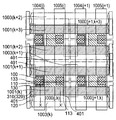
도 5a 및 도 5b는 본 발명의 메모리 셀들이 어레이 구조를 형성하도록 배열 및 접속된 평면도 및 셀 부분의 단면도.5A and 5B are plan views and cross-sectional views of a cell portion in which memory cells of the present invention are arranged and connected to form an array structure;
도 6a 내지 도 6g는 도 5a 및 도 5b에 도시한 실시예의 메모리 셀들 및 어레이를 제조하는 공정의 예를 도시한 단면도.6A-6G are cross-sectional views illustrating examples of processes for fabricating memory cells and arrays of the embodiments shown in FIGS. 5A and 5B.
도 7은 도 5a 및 도 5b에 도시한 메모리 셀 어레이의 등가 회로도.FIG. 7 is an equivalent circuit diagram of the memory cell array shown in FIGS. 5A and 5B.
도 8은 기입 비트라인 및 독출 비트라인이 공유되는 메모리 셀들 및 어레이의 평면도.8 is a plan view of an array of memory cells and array in which write bit lines and read bit lines are shared;
도 9는 도 8의 메모리 셀 어레이의 등가 회로도.FIG. 9 is an equivalent circuit diagram of the memory cell array of FIG. 8. FIG.
<도면의 주요부분에 대한 부호의 설명> <Description of the symbols for the main parts of the drawings>
100; 반도체 박막 101; 제1 주면100; Semiconductor
102; 제2 주면 10; 지지기판102; Second
20; 절연막 110; 제1 반도체 영역20;
120; 제2 반도체 영역 130; 제3 반도체 영역120;
110s; 실리사이드층 220; 제2 게이트 절연막110s; Silicide
300; 도전 게이트 박막 310; 제1 도전 게이트300; A conductive gate
330; 제3 도전 게이트 51; 포토레지스트 패턴330; Third
1000; 메모리 셀 1001; 워드라인1000;
1003; 공통라인1003; Common line
본 발명은 반도체 메모리 및 이로부터 구축된 집적회로에 관한 것으로, 특히 채널 형성 영역을 위해 SOI(Semiconductor On Insulator) 혹은 SON(Semiconductor On Nothing)와 같은 반도체 박막을 사용하는 기술에 관한 것이다. 반도체 박막은 경우에 따라 절연 기판(SOI) 상에 형성되며, 다른 경우엔 공동 상태(SON)에서 기판들에 의해 양단부가 걸려 유지되고, 또 다른 경우엔 기판에 일단부가 접속된 돌출부를 갖는다.BACKGROUND OF THE
에이치. 제이. 완 등은 부분적으로 공핍된 SOIMOS 트랜지스터 구조에 두 개의 상보형 트랜지스터들을 탑재시킴으로써 커패시터를 사용하지 않는 다이내믹 메모리를 얻는 것을 1993년에 제안하였다(예를 들면 비-특허 문헌 1을 참조).H. second. Wan et al. Proposed in 1993 to obtain a dynamic memory without a capacitor by mounting two complementary transistors in a partially depleted SOIMOS transistor structure (see Non-Patent
최근에, 부분 공핍 SOIMOS 트랜지스터의 드레인의 고 전계 영역에서의 눈사태 항복(avalanche breakdown)과 같은 캐리어 증배 현상을 이용하여 캐리어들을 발생시키고 이들 얻어진 캐리어들을 중립의 바디에 충전시키는 데 사용하여 트랜지스터의 드레인과 소스간에 흐르는 전류를 변화시키는 메모리가 제안되었다(예를 들면, 비-특허 문헌 2를 참조).Recently, carrier multiplication phenomena, such as avalanche breakdown in the high field region of the drain of a partially depleted SOIMOS transistor, are used to generate carriers and charge these obtained carriers in a neutral body to A memory for changing the current flowing between the sources has been proposed (see, for example, Non-Patent Document 2).
PD SOI로 약기되는 부분 공핍 SOI라는 용어는 공핍층이 반도체 박막의 깊이 방향으로 부분적으로만 확산하여 이를 중립영역이 되게 한 SOI를 지칭한다. "바디"는 채널이 형성된 전술의 반도체 박막을 간단히 하여 지칭한 용어이다.The term partially depleted SOI, abbreviated as PD SOI, refers to an SOI in which the depletion layer only partially diffuses in the depth direction of the semiconductor thin film to make it a neutral region. "Body" is a term for simply referring to the above-described semiconductor thin film in which a channel is formed.
[비-특허 문헌 1][Non-Patent Document 1]
IEDM(International Electron Device Meeting) 테크니컬 다이제스트, 635 내지 638 페이지에, 에이치. 제이. 시. 후, "SOI 기판 상의 커패시터가 없는 DRAM 셀",International Electron Device Meeting (IEDM) Technical Digest, pp. 635-638. second. city. "DRAM cell without capacitor on SOI substrate",
[비-특허 문헌 2][Non-Patent Document 2]
2002년 2월, IEEE 전자소자 레터, 볼륨 23, 2호, 85-87 페이지에, 에스. 오코닌 등, "커패시터가 없는 1T-DRAM 셀".In February 2002, in IEEE Electronics Letter, Volume 23, No. 2, pages 85-87, S. "1T-DRAM cells without capacitors" such as oconin.
한편, 저 전력 소비용으로 혹은 SOIMOS 트랜지스터의 진보된 소형화를 위해 완전 공핍된(FD) SOI를 사용하는데, 이에 따라 FDSOI에 적용될 수 있는 SOI 메모리 셀들에 필요성이 유발된다. FD(완전 공핍) SOI라는 용어는 그곳에 제작된 트랜지스터의 게이트 바이어스로 반도체 박막의 전체 깊이를 공핍층으로 되게 하는 두께 및 불순물 농도를 갖는 SOI를 지칭한다.On the other hand, fully depleted (FD) SOI is used for low power consumption or for advanced miniaturization of SOIMOS transistors, thereby creating a need for SOI memory cells that can be applied to FDSOI. The term FD (Full Depletion) SOI refers to an SOI having a thickness and an impurity concentration that causes the entire depth of the semiconductor thin film to be a depletion layer by the gate bias of a transistor fabricated therein.
또한 드레인의 고 전계 부분에서의 캐리어 증배를 이용하는 방법으로 인해서, 신호가 기입될 셀의 드레인을 고 전압으로 구동시키기 위해 비트 라인에 접속되는 비선택된 셀 내에 약간의 캐리어 증배가 야기된다. 이로 인해 "기입 교란"이라 하는, 경미할지라도, 오기입으로 되어, 다수 셀들이 각 비트 라인에 접속되는 대형 어레이를 조립하기가 어렵게 된다. 게다가, 상기 방법은 상대적으로 큰 전류를 필요로 하게 되고, 다수의 셀의 병렬 프로그래밍을 막게 된다.Also, the method of using carrier multiplication in the high electric field portion of the drain causes a slight carrier multiplication in an unselected cell connected to the bit line to drive the drain of the cell to which the signal is to be written to the high voltage. This results in a slight, if not written, "write disturb" that makes it difficult to assemble a large array in which multiple cells are connected to each bit line. In addition, the method requires a relatively large current and prevents parallel programming of multiple cells.
본 발명은 전술한 바에 비추어 된 것으로, 본 발명의 목적은 FDSOI에 적용 가능한 커패시터가 없는 SOI 혹은 이 외 반도체 박막 메모리 셀 및 메모리 셀을 제공하는 것이다. 본 발명의 또 다른 목적은 드레인의 고 전계 부분에서의 캐리어 증배를 사용하지 않고 데이터가 기입 또는 소거되는 SOI 혹은 이 외 반도체 박막 메모리 셀 및 메모리 셀과, 메모리 셀 및 어레이에 대한 동작 방법 및 제조방법을 제공하는 것이다.SUMMARY OF THE INVENTION The present invention has been made in light of the foregoing, and an object of the present invention is to provide a capacitor-free SOI or other semiconductor thin film memory cell and a memory cell applicable to FDSOI. It is still another object of the present invention to provide an SOI or other semiconductor thin film memory cell and memory cell in which data is written or erased without using carrier multiplication in the high electric field portion of the drain, and an operation method and a manufacturing method for the memory cell and array. To provide.
전술의 목적들을 달성하기 위해서, 본 발명은 드레인 혹은 소스가 아닌 제3 반도체 영역으로부터의 캐리어들을 (1) 바디에, (2) 드레인의 고 전계 부분 내 캐리어 증배를 사용함이 없이, 공급하는 방법을 채용한다.In order to achieve the above objects, the present invention provides a method of supplying carriers from a third semiconductor region that is not a drain or a source to (1) the body, without (2) using carrier multiplication in the high electric field portion of the drain. Adopt.
실시형태Embodiment
본 발명의 메모리 셀을 도 1 및 도 2a와 도 2b에 도시하였다. 도 1은 본 발명의 반도체 셀의 단면도의 예이다. 도 2a는 평면도의 예이고 도 2b는 도 2a의 X-X' 선을 따라 취한 단면도이다. 이들 도면들에 도시한 바와 같이, 메모리 셀은, The memory cell of the present invention is shown in FIGS. 1 and 2A and 2B. 1 is an example of a cross-sectional view of a semiconductor cell of the present invention. FIG. 2A is an example of the top view and FIG. 2B is a sectional view taken along the line X-X 'of FIG. 2A. As shown in these figures, the memory cell,
제1 주면(principal surface)(101)과 이 제1 주면과 면하여 있는 제2 주면(102)을 구비한 반도체 박막(100);A semiconductor
반도체 박막의 제1 주면 상에 형성된 제1 게이트 절연막(210);A first
제1 게이트 절연막 상에 형성된 제1 도전 게이트(310);A first
제1 도전 게이트에 걸쳐 서로 떨어져 있고, 제1 도전 게이트와는 절연되어 있으며, 반도체 박막(100)과는 접촉하여 있고, 제1 도전형을 갖는 제1 반도체 영역(110) 및 제2 반도체 영역(120); 및A
역도전형을 가지며 반도체 박막과 접촉하여 있는 제3 반도체 영역(130)을 포함한다.And a
반도체 박막(100)은 제1 도전 게이트 밑의 제1 반도체 영역과 제2 반도체 영역 사이의 제1 주면(101)과 제2 주면(102) 사이에 캐리어들의 공핍이 생기게 하는 제1 도전 게이트의 전위가 존재하는 두께 및 불순물 농도 관계의 조합을 갖는다.The semiconductor
본 발명에 의해 제공된 메모리 셀에서, 반도체 박막은 제1 반도체 영역(110)과 제2 반도체 영역(120) 사이에 개재되어 있고 103으로 표기된 반도체 박막부분으로부터 제3 반도체 영역(130)으로 확장되어 있고, 104로 표기된 반도체 박막의 이 확장된 부분 상에는 제2 게이트 절연막(220)이 형성되고 이 제2 게이트 절연막(220) 상에는 제2 도전 게이트(320)가 형성되어 있다.In the memory cell provided by the present invention, the semiconductor thin film is interposed between the
도 2a 및 도 2b에서, 참조부호 421은, 필요하다면, 서로 오버랩되는 제1 도전 게이트와 제2 도전 게이트를 절연시키기 위해 설치되는 게이트간 절연막을 나타낸다. 참조부호 400은 소위 필드 절연막이다. 참조부호 413 및 431은 제3 반도체 영역 상에 형성된 절연막 및 제1 도전 게이트 상의 절연막을 각각 나타낸다. 113, 123, 133, 313, 323은, 필요하다면, 제1, 제2, 제3 반도체 영역들에 이르고 제1 및 제2 도전 게이트들에 이르는 콘택들로서 작용하도록 설치된다. 도 1은 도 2a의 Y-Y' 선을 따라 취한 단면도에 해당한다. 이러한 셀이 전술한 콘택들을 반드시 갖출 필요는 없다. 특히, 도전 게이트에 이르는 콘택은 도전 게이트가 빈번히 워드 라인의 일부를 구성하기 때문에 다수의 셀들 간에 공유될 수 있다.2A and 2B,
제1 도전 게이트의 게이트 임계전압을 넘는 전위에 의해 제1 반도체 영역(110)과 제2 반도체 영역(120) 사이에 개재된 반도체 박막 부분에 제1 도전형 채널이 야기된다. 본 발명에서는, 반도체 박막 부분(103)을 제1 채널 형성 반도체 박막 부분이라 한다.The first conductivity type channel is caused in a portion of the semiconductor thin film interposed between the
반도체 박막 확장부분(104)에는 역도전형의 캐리어들이 유발되거나, 역도전형의 캐리어들용의 채널이 제2 도전 게이트와 제3 반도체 영역간 전위 차에 의해 형성된다. 확장부분(104)을 본 발명에서는 제2 채널 형성 반도체 박막부분이라 한다. 제2 도전 게이트에서 보아 역도전형인 캐리어 채널의 게이트 임계 전압을 조정하기 위해서 확장부분(104)에, 다른 확장부분(104)과는 도전형이 다르거나 불순물 농도가 다른 부분(105)을 형성할 수도 있다. 본 발명에서, 전술한 "게이트 임계전압을 넘는 전위"라는 것은 트랜지스터가 n채널 트랜지스터인 경우 절대값이 정의 방향으로 게이트 임계 전압보다 큰 전위 및 트랜지스터가 p채널 트랜지스터인 경우엔 부의 방향으로 게이트 임계 전압보다는 절대값이 큰 전위를 의미한다.In the semiconductor
제1 주면과 제2 주면간 거리를, 본 발명에서는 반도체 박막의 두께라 한다. The distance between the first main surface and the second main surface is referred to as the thickness of the semiconductor thin film in the present invention.
제2 도전 게이트의 전위와 제3 반도체 영역의 전위의 제1 조합에 의해서, 제1 도전 게이트에서 본 제1 채널 형성 반도체 박막부분 내 제1 도전형 채널의 게이트 임계 전압을 제1 값(Vth11)으로 변경하기 위해, 역도전형의 캐리어들(2)을 제2 채널형성 반도체 박막부분을 통해 제3 반도체 영역으로부터 제1 채널형성 반도체 박막 부분에 주입한다. 이 동작을 본 발명에서는 "기입"이라 한다.According to the first combination of the potential of the second conductive gate and the potential of the third semiconductor region, the gate threshold voltage of the first conductive channel in the first channel forming semiconductor thin film portion viewed from the first conductive gate is changed to the first value Vth 11. In order to change),
제1 조합의 전위들에 따라서, 제2 도전 게이트의 전위에서 제3 반도체 영역의 전위를 감하여 얻어진 값은 제3 반도체 영역으로부터 역도전형의 캐리어들이 이동되게 제2 채널형성 반도체 박막 부분 내 유발되는 채널의 게이트 임계전압 (Vth2r)을 초과한다. Vth2r은 제2 도전 게이트에서 본 게이트 임계전압이다.According to the potentials of the first combination, a value obtained by subtracting the potential of the third semiconductor region from the potential of the second conductive gate is a channel induced in the second channel forming semiconductor thin film portion to move the carriers of the reverse conductivity from the third semiconductor region. Exceeds the gate threshold voltage of Vth 2r . Vth 2r is the gate threshold voltage seen from the second conductive gate.
역도전형의 캐리어들이 제1 채널형성 반도체 박막부분에 주입됨으로써, 제1 도전 채널이 생기도록 하는 제1 도전 게이트에 필요한 게이트 전압은 역도전형의 주입된 캐리어들의 수 혹은 전하들의 수에 대응하는 레벨만큼 감소된다. 이것은 게이트 임계 전압이 등가로 공핍형 쪽으로 옮겨졌음을 의미한다. 게이트 임계 전압이 개선형의 범위 내에서 변경되었다면, 이것은 게이트 임계 전압의 절대값이 감소된 것임을 의미한다.As the carriers of the reverse conductivity type are injected into the first channel forming semiconductor thin film portion, the gate voltage required for the first conductive gate to generate the first conductive channel is a level corresponding to the number of carriers or charges injected into the reverse conductivity type. Is reduced. This means that the gate threshold voltage has been shifted to the depletion equivalent. If the gate threshold voltage is changed within the range of the improved type, this means that the absolute value of the gate threshold voltage is reduced.
제1 전위 조합으로 복수 레벨 설정이 가능하다. 예를 들면, 제2 도전 게이트의 전위에서 제3 반도체 영역의 전위를 감하여 얻어진 값이 제3 반도체 영역에서 역도전형 캐리어들이 이동되게 제2 채널형성 반도체 박막부분에 유발되는 채널의, 제2 도전 게이트에서 보았을 때, 게이트 임계전압(Vth2r)을 충분히 초과한다는 전제에서, 게이트 전위에 관하여 제3 반도체 영역의 전위는 복수 레벨로 설정된다. 이에 따라, 제1 도전 게이트에서 본 제1 도전 채널의 게이트 임계전압을 기입용의 복수 레벨의 값들 Vth11, Vth12, Vth13,...로 변경하는 것이 가능하다. 요약하여 한 셀에 복수 비트 정보를 저장하는 것을 가능하게 한다.Multiple level settings are possible with the first potential combination. For example, a value obtained by subtracting the potential of the third semiconductor region from the potential of the second conductive gate is the second conductive gate of the channel induced in the second channel forming semiconductor thin film portion such that the reverse conductive carriers are moved in the third semiconductor region. As seen from the above, on the premise that the gate threshold voltage Vth 2r is sufficiently exceeded, the potential of the third semiconductor region is set to a plurality of levels with respect to the gate potential. Accordingly, it is possible to change the gate threshold voltage of the first conductive channel seen from the first conductive gate into values Vth 11 , Vth 12 , Vth 13 ,..., For writing. In summary, it is possible to store multiple bit information in one cell.
제1 채널형성 반도체 박막에 주입된 역도전형 캐리어들(2)은 제1 도전형의 캐리어들과의 재결합으로 인해서, 혹은 자체 필드에 기인한 제1 채널형성 반도체 박막으로부터 유출됨에 따라 점차로 감소한다. 따라서, 제1 채널형성 반도체 박막부분 내 축적된 반대 도전 캐리어들의 양을 읽고 판독에 기초하여 재기입하는 것이 필요하다. 이것을 "리프레쉬"라 한다.The reverse
제2 도전 게이트의 전위와 제3 반도체 영역의 전위의 제2 조합에 의해, 제1 도전 게이트에서 본 제1 채널형성 반도체 박막부분 내 제1 도전형 채널의 게이트 임계전압을 제2 값(Vth10)으로 변경하기 위해, 역도전형의 캐리어들(2)을 제1 채널형성 반도체 박막부분으로부터 제3 반도체 영역으로 끌어낸다. 이 동작을 본 발명에서는 "소거"라 한다.By the second combination of the potential of the second conductive gate and the potential of the third semiconductor region, the gate threshold voltage of the first conductive channel in the first channel forming semiconductor thin film portion viewed from the first conductive gate is changed to the second value Vth 10. To reverse), the
제2 조합의 전위관계에 따라서, 제2 도전 게이트의 전위에서 제1 채널형성 반도체 박막부분에 주입된 역도전형의 전위를 감하여 얻어진 값은 제2 도전 게이트에서 본 제2 채널형성 반도체 박막부분 내 역도전형의 게이트 임계전압 (Vth2r)을 초과한다.According to the potential relationship of the second combination, the value obtained by subtracting the potential of the reverse conductive type injected into the first channel-forming semiconductor thin film portion from the potential of the second conductive gate is the weight factor in the second channel-forming semiconductor thin film portion viewed from the second conductive gate. Exceeds the typical gate threshold voltage (Vth 2r ).
대안으로, 역도전형의 캐리어들을 제1 혹은 제2 반도체 영역으로 이끌어 들 이는 방향의 전위(예를 들면, 정공들에 대해선 부의 방향으로 0.6V 이상)를 부여함으로써 소거 동작이 달성된다. 이 경우, 재결합을 통해 역도전형의 캐리어들의 감소를 가속화하기 위해서 제1 도전형의 캐리어들이 제1 채널형성 반도체 박막부분에 또한 공급된다. 이 소거동작에서, 공통 라인 혹은 비트 라인에 제2 반도체 영역 혹은 제1 반도체 영역이 접속된 모든 셀로부터 데이터가 소거된다.Alternatively, the erase operation is achieved by applying a potential in the direction of drawing the reverse conductive carriers to the first or second semiconductor region (eg, 0.6 V or more in the negative direction with respect to the holes). In this case, carriers of the first conductivity type are also supplied to the first channeling semiconductor thin film portion to accelerate the reduction of the carriers of the reverse conductivity through recombination. In this erasing operation, data is erased from all the cells in which the second semiconductor region or the first semiconductor region is connected to the common line or the bit line.
본 발명의 메모리 셀에 저장된 정보는 역도전형의 캐리어들이 메모리 셀의 제1 채널형성 반도체 박막에 저장되어있는지 여부에 의해 혹은 저장량으로부터 판정된다. 저장된 정보를 이러한 식으로 판정하기 위해서, 제2 반도체 영역에 관한 제1 도전 게이트의 전압은 제1 게이트 임계 전압 및 제2 게이트 임계전압 중 하나 혹은 이들 모두를 초과하는 규정된 값으로 설정되고 제1 반도체 영역과 제2 반도체 영역간에 흐르는 전류가 큰지 아니면 작은지가 검출된다("작다는 것"은 제로를 포함한다). 예를 들면, 제2 반도체 영역에 관한 제1 도전 게이트의 전압은 제1 게이트 임계전압 내지 제2 게이트 임계전압 범위 내 레벨로 설정되고 제1 반도체 영역과 제2 반도체 영역 사이에 전류가 흐르는지 여부를 검출하여 저장된 정보를 판정한다.The information stored in the memory cell of the present invention is determined by the amount of storage or whether the carriers of the reverse conductivity type are stored in the first channel forming semiconductor thin film of the memory cell. To determine the stored information in this way, the voltage of the first conductive gate with respect to the second semiconductor region is set to a prescribed value exceeding one or both of the first gate threshold voltage and the second gate threshold voltage and the first It is detected whether the current flowing between the semiconductor region and the second semiconductor region is large or small ("small" includes zero). For example, the voltage of the first conductive gate with respect to the second semiconductor region is set at a level within the range of the first gate threshold voltage to the second gate threshold voltage and whether a current flows between the first semiconductor region and the second semiconductor region. To detect the stored information.
제1 임계 전압들의 복수 레벨들이 기입되는 경우에, 저장된 데이터를 식별하기 위해서 제1 도전 게이트의 전압을 이들 레벨들 중에서 어떤 두 레벨 간 레벨로 설정한다. 대안으로, 제2 반도체 영역에 관한 제1 도전 게이트의 전압은 제1 게이트 임계 전압 및 제2 게이트 임계전압 모두를 초과하는 전압으로 설정되고 저장된 정보는 제1 반도체 영역과 제2 반도체 영역간에 흐르는 전류의 량으로부터 판정된 다.When multiple levels of the first threshold voltages are written, the voltage of the first conductive gate is set to a level between any two of these levels to identify stored data. Alternatively, the voltage of the first conductive gate with respect to the second semiconductor region is set to a voltage exceeding both the first gate threshold voltage and the second gate threshold voltage and the stored information is a current flowing between the first semiconductor region and the second semiconductor region. Determined from the quantity
전류를 검출하기 위해서, 기준전류와 비교기 회로를 사용하는 비교검출, 혹은 비트라인 또는 추가적인 용량을 가지는 비트 라인을 충전 혹은 방전하는 시정수에 의한 검출 등의 공지의 방법이 채용될 수 있다. 이 동작을 '독출'이라 한다.In order to detect the current, a known method such as comparison detection using a reference current and a comparator circuit, or detection by a time constant for charging or discharging a bit line or a bit line having an additional capacity can be adopted. This operation is called 'read'.
독출동작을 통해, 제1 채널형성 반도체 박막부분의 에너지대 내 가전자대와 전도대의 전위는 역도전형의 캐리어들을 소거하는 방향으로 옮겨진다. 또한, 제1 채널형성 반도체 박막부분 내 저장된 역도전형 캐리어들의 재결합을 가속화시키고 경우에 따라서는 정보손실이 되게 하기 위해서 대량의 제1 도전형 캐리어들이 제1 채널형성 반도체 박막부분에 공급된다. 이 경우, 독출 직후에 리프레쉬 동작이 행해져야 한다.Through the read operation, the potential of the valence band and the conduction band in the energy band of the first channel-forming semiconductor thin film portion is shifted in the direction of erasing carriers of the reverse conductivity type. Also, a large amount of first conductive carriers are supplied to the first channeling semiconductor thin film portion to accelerate the recombination of the reverse conductive carriers stored in the first channeling semiconductor thin film portion and in some cases to lose information. In this case, the refresh operation should be performed immediately after reading.
도 1에 반도체 박막(100)은 이의 표면에 절연막(20)이 형성된 기판(10)에 의해 지지되어 있다. 대부분의 경우에, 기판(10)은 실리콘으로 형성되고 절연막(20)은 산화실리콘막이다. 표면에 절연층을 구비한 지지기판을 절연기판이라 한다. 이를테면 석영기판과 같이 완전히 절연물질로 형성된 절연기판 또한 지지기판으로서 사용될 수 있다. 대안으로서의 구조는 반도체 박막의 적어도 일 단부, 혹은 제1 반도체 영역이나, 제2 반도체 영역, 또는 제3 반도체 영역의 단부가 기판에 의해 지지되는 구조이다.1, the semiconductor
본 발명에서, 기입동작, 소거동작, 독출동작 중에 제1 도전 게이트의 전압 및 제2 도전 게이트의 전압을 주의하여 선택한다면, 각 동작모드에 동일한 전압을 사용할 수 있다. 그러면 제1 및 제2 도전 게이트들을 연속하게 혹은 도 3에 예를 보인 바와 같이 공유되게 할 수 있다. 또한, 게이트 절연막들에 동일한 물질 및 두께를 채용할 수 있다. 결국, 제조단계 수 및 셀이 점유하는 면적이 감소된다. 이 경우, 본 발명의 기입동작 및 소거동작에 관한 설명에서 '제2 도전 게이트'를 '제1 도전 게이트'로 대치시킴으로써, 기입동작 및 소거동작을 실현하는 것이 가능해진다.In the present invention, if the voltage of the first conductive gate and the voltage of the second conductive gate are carefully selected during the write operation, the erase operation, and the read operation, the same voltage can be used for each operation mode. The first and second conductive gates can then be continuously or shared as shown in FIG. 3. In addition, the same material and thickness may be employed as the gate insulating layers. As a result, the number of manufacturing steps and the area occupied by the cell are reduced. In this case, in the description of the write operation and the erase operation of the present invention, it is possible to realize the write operation and the erase operation by replacing the 'second conductive gate' with the 'first conductive gate'.
본 발명에서 어떤 조건 하에서 제1 게이트 임계 전압 값을 기입하고 어떤 또 다른 조건 하에서 제2 게이트 임계 전압 값을 기입하는 것이 또한 가능하다. 예를 들면, 제1 게이트 임계 전압은, 제3 반도체 영역의 전위가 제2 반도체 영역의 전위에 관하여 순방향으로 바이어스된 상태에서, 제2 도전 게이트의 전위에서 제3 반도체 영역의 전위를 감하여 얻어진 값이, 제2 도전 게이트에서 본 제3 반도체 영역으로부터 역도전형의 캐리어들이 이동되게 제2 채널형성 반도체 박막부분에 형성되는 채널의 게이트 임계 전압(Vth2r)을 초과할 때 기입된다. 반면, 제2 게이트 임계전압은 제3 반도체 영역의 전위가 제로로 바어이스되거나 제2 게이트 전압에 관하여 역방향으로 바이어스되었을 때 기입(소거와 같음)된다.It is also possible in the present invention to write the first gate threshold voltage value under certain conditions and to write the second gate threshold voltage value under some other conditions. For example, the first gate threshold voltage is a value obtained by subtracting the potential of the third semiconductor region from the potential of the second conductive gate while the potential of the third semiconductor region is forward biased with respect to the potential of the second semiconductor region. This is written when the gate threshold voltage Vth 2r of the channel formed in the second channel forming semiconductor thin film portion is moved so that carriers of the reverse conductivity type are moved from the third semiconductor region seen from the second conductive gate. On the other hand, the second gate threshold voltage is written (equivalent to erasing) when the potential of the third semiconductor region is zeroed or biased in reverse with respect to the second gate voltage.
본 발명을 효과적으로 수행하는 바람직한 또 다른 실시예는 도 4a 및 도 4b에 도시한 메모리 셀이다. 메모리 셀은,Another preferred embodiment for effectively carrying out the present invention is the memory cell shown in FIGS. 4A and 4B. Memory cells,
제1 주면(101)과 이 제1 주면에 면하는 제2 주면(102)을 구비한 반도체 박막(부분들(103, 104)로 나뉘어져 있음);A semiconductor thin film having a first
반도체 박막의 제1 주면 상에 형성된 제1 게이트 절연막(210);
A first
상기 제1 게이트 절연막 상에 형성된 제1 도전 게이트(310);A first
상기 제1 도전 게이트에 걸쳐 서로 떨어져 있고, 상기 제1 도전 게이트로부터 절연되어 있으며, 상기 반도체 박막과 접촉하여 있고, 제1 도전형을 갖는 제1 반도체 영역(110) 및 제2 반도체 영역(120);A
반대되는 도전형을 가지며 상기 반도체 박막과 접촉하여 있는 제3 반도체 영역(130);A
상기 제1 반도체 영역과 상기 제2 반도체 영역 사이에 개재된 상기 반도체 박막부분(제1 채널형성 반도체 박막부분)의 상기 제2 주면 상에 형성된 제3 게이트 절연막(230); 및A third
상기 제3 게이트 절연막(230)과 접촉한 제3 도전 게이트(330)를, 적어도 포함하는 것을 특징으로 한다. 본 발명에서 반도체 박막부분(104)은 제2 채널형성 반도체 박막부분이라고도 한다.And at least a third
제1 채널형성 반도체 박막부분에 유기된 역도전형 캐리어들에 관하여 제3 도전 게이트에서 본 게이트 임계 전압인 게이트 임계 전압(Vth3r)을 초과하는 전위가 제3 도전 게이트에 부여되었다면 역도전형의 캐리어들이 제1 채널형성 반도체 박막 내에 안정하게 저장된다. 그러나, 소거 동작 후에 열적 여기, 정규 전계에서의 약간의 캐리어 증배 등에 의해 역도전형의 캐리어들이 점차로 발생되어 제1 채널형성 반도체 박막부분에 저장되므로, 이 경우에도 리프레시 동작이 필요하다.If the potential of the reverse conductive carriers induced in the first channel forming semiconductor thin film portion exceeds the gate threshold voltage Vth 3r , which is the gate threshold voltage seen from the third conductive gate, the reverse conductive carriers are applied. It is stably stored in the first channel forming semiconductor thin film. However, since the reverse conduction carriers are gradually generated and stored in the first channel forming semiconductor thin film portion due to thermal excitation, slight carrier multiplication in a normal electric field, etc. after the erase operation, a refresh operation is also required in this case.
도 4a는 본 실시예의 박막 메모리 셀의 평면도이고 도 4b는 도 4a의 평면도 의 X-X'선을 따라 취한 단면도이다. 도 4a 및 도 4b에서, 참조부호 10은 지지기판을 나타내고, 20은 지지기판(10)의 표면상의 절연막을 나타낸다. 103 및 104는 각각 반도체 박막(100)의 부분인 제1 및 제2 채널형성 반도체 박막부분이다. 210 및 220은 반도체 박막부분들(103, 104) 상에 형성된 게이트 절연막들을 나타낸다. 도면에서 게이트 절연막들(210, 220)은 연속하여 있다. 310은 제2 도전 게이트로부터 또한 연속하여 있는 제1 도전 게이트를 나타낸다. 110 및 120은 각각 제1 및 제2 반도체 영역들이다. 130은 제3 반도체 영역을 나타낸다.4A is a plan view of the thin film memory cell of this embodiment, and FIG. 4B is a cross-sectional view taken along the line X-X 'of the plan view of FIG. 4A. 4A and 4B,
113 및 123은 각각 제1 및 제2 반도체 영역들에 이르는 배선 콘택들을 나타낸다. 133은 제3 반도체 영역에 이르는 배선 콘택을 나타낸다. 400은 상호접속 막 등의 밑에 놓인 소위 필드 절연막이다. 431은 제1 도전 게이트 상에 절연막이고 410은 반도체 박막(100)과 절연막(20) 사이에 놓인 절연막을 나타낸다. 313은 제1 도전 게이트에 이르는 배선 콘택을 나타낸다. 333은 필요하다면 제3 도전 게이트에 이르도록 설치된 배선 콘택을 나타낸다.113 and 123 represent wiring contacts leading to the first and second semiconductor regions, respectively. 133 represents a wiring contact leading to the third semiconductor region. 400 is a so-called field insulating film underlying the interconnect film or the like.
각 셀이 전술한 콘택들을 구비하는 것이 항시 필요한 것은 아니다. 특히, 도전 게이트에 이르는 콘택은 도전 게이트가 빈번히 워드 라인의 일부를 구성하므로 다수의 셀들 간에 공유될 수 있다. 불순물 영역(105)은 제3 도전 게이트의 전계가 반도체 박막부분(103)보다 덜 반도체 박막부분(104)에 영향을 미친다면(즉, 제3 도전 게이트가 도 4b에 도시한 바와 같이 반도체 박막부분(104)과 중첩하지 않는다면, 혹은 제3 게이트 절연막(230)보다 두꺼운 절연막이 이들 사이에 개재된 상태에서 제3 도전 게이트가 반도체 박막부분(104)과 중첩한다면), 항시 필요한 것은 아니다.It is not always necessary for each cell to have the contacts described above. In particular, the contact to the conductive gate can be shared among a plurality of cells since the conductive gate frequently forms part of the word line. The
전술한 실시형태들에서, 제1 및 제2 도전 게이트들은 제2 채널형성 반도체 박막의 불순물의 도전형 혹은 불순물 농도, 혹은 제2 도전 게이트 물질이 제1 채널형성 반도체 박막의 불순물의 유형 혹은 불순물 농도, 혹은 제1 도전 게이트 물질과 다르다면 다른 게이트 임계 전압들을 가질 수 있다. 제2 채널형성 반도체 박막부분에 주입된 역도전형 캐리어들은 제3 반도체 영역과는 반대되는 도전형의 캐리어들용의 채널에 관한 제2 도전 게이트의 게이트 임계 전압이 제1 도전 게이트의 게이트 임계 전압보다 개선형 방향으로 높은 레벨로 설정된다면 제3 반도체 영역으로 역으로 흐르는 것이 방지된다.In the above-described embodiments, the first and second conductive gates may be conductive or impurity concentrations of impurities in the second channel forming semiconductor thin film, or the second conductive gate material may be impurity types or impurity concentrations in the first channel forming semiconductor thin film. Or may have different gate threshold voltages if different from the first conductive gate material. In the reverse conductive carriers injected into the second channel forming semiconductor thin film portion, the gate threshold voltage of the second conductive gate in relation to the channel for the carriers of the conductive type opposite to the third semiconductor region is greater than the gate threshold voltage of the first conductive gate. If set to a high level in the improved direction, the reverse flow to the third semiconductor region is prevented.
실시예Example
제1 도전형을 n형으로 하고 역도전형을 p형으로 하여 메모리 셀 동작을 이하 기술한다. 다음의 설명에서 제공되는 원리 및 효과는 변경의 극(polarity)과 방향이 반대로 되겠지만, 제1 도전형이 p형인 경우에도 적용된다. 도 5a는 본 발명의 메모리 셀들 및 메모리 셀들의 어레이의 실시예에 대한 평면도이다. 도 5b는 도 5a의 평면도의 X-X'선을 따라 취한 단면도이다.The memory cell operation is described below with the first conductivity type being n type and the reverse conductivity type being p type. The principles and effects provided in the following description will be reversed in polarity and direction of change, but also apply when the first conductivity type is p-type. 5A is a top view of an embodiment of a memory cell and an array of memory cells of the present invention. FIG. 5B is a cross-sectional view taken along the line X-X 'of the plan view of FIG. 5A.
참조부호 10은 이 예에서 고저항의 n형 실리콘 <100> 평면 웨이퍼인 지지기판을 나타낸다. 20은 약 100nm의 두께를 가진 산화실리콘막이다. 103은 이 실시예에서 박막 메모리 셀(1000)의 제1 채널형성 반도체 박막부분으로서 작용하는 약 30nm 두께의 반도체 박막을 나타낸다. 104는 제2 채널형성 반도체 박막부분을 나타낸다. 105는 제2 채널형성 반도체 박막부분의 고 불순물 농도를 나타낸다. 110은 드레인(제1 반도체 영역)을 나타낸다. 114는 드레인 확장부이다. 120은 소스(제2 반도체 영역)이다. 124는 소스 확장부이다. 130은 역도전형의 제3 반도체 영역이다. 210은 2.7nm 두께의 제1 게이트 질화산화막(nitrided oxide film)이다. 220은 제2 게이트 질화산화막이다. 310 및 320은 제1 도전 게이트 및 이 제1 연속 게이트에 연속한 제2 도전 게이트이다. (300은 도전 게이트 박막으로서의 기호이다. 1001은 로컬 워드 라인으로서의 기능 기호이다).
210 및 220은 연속한 게이트들이다. 제1 도전 게이트는 이 실시예에서 길이가 약 100nm이고, 붕소가 첨가된 실리콘 박막으로부터 형성된다. 제1, 제2, 제3 반도체 영역들은 반도체 박막 상에 에피택셜 성장에 의해 형성된 반도체 막을 포함한다. 한 셀 내 제1 및 제2 채널형성 반도체 박막부분들(103, 104)은 이격 절연막(401)에 의해 인접 셀 내 제1 및 제2 채널형성 반도체 박막부분들(103, 104)로부터 이격되어 있다.210 and 220 are consecutive gates. The first conductive gate is about 100 nm in length in this embodiment and is formed from a silicon thin film to which boron is added. The first, second and third semiconductor regions include a semiconductor film formed by epitaxial growth on a semiconductor thin film. The first and second channel forming semiconductor
113은 제1 반도체 영역에 이르는 콘택이고, 콘택은 독출 비트 라인(1005)에 접속된다. 113은 제3 반도체 영역에 이르는 콘택을 나타내며, 콘택은 기입 비트 라인(1004)에 접속된다. 연속하여 있는 제1 및 제2 도전전극들(310(320))은 워드 방향으로 셀들 사이에 연속하여 연장되어 있어 로컬 워드 라인(1001)을 형성한다. 제2 반도체 영역은 워드 방향으로 셀들 사이에 연장되어 있어 로컬 공통 라인(1003)을 형성한다. 로컬 워드 라인 및 로컬 공통 라인은 직접적인 저항이 어레이 동작에 영향을 미치지 않는 한 연장되고, 각각은 선택 트랜지스터를 통해서 혹은 직접 전역의 워드 라인 및 전역의 공통 라인에 접속된다. 대형 용량 어레이에서, 전술한 두 유형들의 비트 라인들은 이들의 각각의 전력의 비트 라인들에 선택 트랜지스터를 통해 접속된다.113 is a contact leading to the first semiconductor region, and the contact is connected to the read
도 5a의 어레이 구성에서, 셀들(1000)은 비트 방향으로 미러 이미지 관계로 반복하여 배열된다. 결국, 비트 방향으로 서로 인접한 셀들 간에 콘택들(113, 133)이 공유된다. 제1 및 제3 반도체 영역들은 한 셀에서 비트 방향의 일 방향으로 이의 인접한 셀로 연속하여 있다. 이에 따라 어레이 면적이 감소된다. 도 5a는 워드 방향으로 두 개의 셀들 및 비트 방향으로 4개의 셀들로 해서, 총 8개의 셀들(셀(1000(j, k),...,셀(1000)(j+1, k+3))을 도시한 것이다. 셀들의 미러 이미지 배열을 후술하는 도 8의 실시예에서 채용된다. In the array configuration of FIG. 5A, the
이 실시예의 제조공정을 도 6a 내지 도 6g 및 도 5b의 단면도를 참조하여 이하 설명한다.The manufacturing process of this embodiment will be described below with reference to the cross-sectional views of FIGS. 6A-6G and 5B.
(a) 고저항 실리콘웨이퍼를 지지기판(10)으로서 사용하고, 약 100nm의 두께의 산화실리콘막(20) 및 약 2 x 10¹⁷ atoms/cc의 n형 불순물 농도와 약 35nm의 두께를 갖는 실리콘 박막(100)을 기판 상에 적층하여 SOI 기판을 준비한다.(a) Silicon having a
(b) 이와 같이 하여 얻어진 SOI 상에, 열 산화에 의해 약 7nm의 두께가 될 때까지 산화막(41)이 성장되게 하고 이 위에 약 50nm의 두께의 질화실리콘막(42)을 CVD로 형성한다. 그 후에, 메모리 셀들이 워드 방향 및 비트 방향으로 접속되는 영역들, 선택 트랜지스터 영역들 및 주변회로 영역들 등의 실리콘 박막의 필요한 부분들을 보호하도록 공지의 포토리소그래피에 의해 포토레지스트 패턴(51)을 형성한다.(b) On the SOI thus obtained, the oxide film 41 is grown until thermally oxidized to a thickness of about 7 nm, and a
(c) 포토레지스트 패턴(51)을 마스크로서 사용하여, 산화실리콘막을 남겨두도록 산화실리콘막에 관하여 선택비를 제공하는 에칭조건 하에서 질화실리콘막을 에칭한다. 이어서, 포토레지스트 패턴을 제거하고 기판표면을 세정한다. 질화실리콘막의 제거에 의해 노출된 산화실리콘막의 노출된 표면을, 산화실리콘막(401)이 약 60nm의 두께로 성장할 때까지 열에 의한 산화로 산화시킨다. 이 단계를 통해서, 실리콘 박막(100)이 여러 부분으로 분할되어 앞에서 주어진 필요한 부분들이 남게 된다.(c) Using the
대안으로, 공지의 STI(얕은 트렌치 분리) 기술을 사용하여 실리콘 박막을 분할할 수도 있다. 평면방향으로 실리콘 박막을 분할하는 절연막을 절연 분리막(401)이라 한다.Alternatively, the silicon thin film may be divided using known STI (shallow trench isolation) techniques. An insulating film dividing the silicon thin film in the planar direction is called an insulating
질화실리콘막(42)을 고온의 인산 기반 에칭액으로 제거하고 산화 실리콘막(41)은 버퍼 불화수소산 기반의 에칭액으로 제거하여 실리콘 박막(100)의 표면을 노출시킨다.The
실리콘 박막(100)의 표면에 열 산화에 의해 2.7nm의 두께로 산화실리콘막(200)이 형성된다. 이후에, ECR(Electron Cyclotron Resonance), ICP(Inductively Coupled Plasma), 등 이 외 고밀도 플라즈마 장치를 사용해서, 질소가스, 수소가스, 혹은 크세논 가스의 플라즈마로부터 질소 래디컬을 기판표면에 유입시키고 기판온도를 400℃로 설정함으로써 5 내지 7%의 질화비로 표면을 질화(nitridation)한다. 이어서, 기판을 고순도 질소가스 분위기 내에 이송시키고 표면 결함들을 어닐링하기 위해 질소 내에서 800℃로 열처리를 행한다. 이와 같이 질화된 산화실리콘막은 제1 및 제2 게이트 산화막으로서 사용된다.The
(d) 다음에, 도전 게이트 박막(300)을 피착에 의해 형성한다. 초기의 10nm 등에 대해서는, 순수 실리콘을 피착하여 순수 실리콘 박막(301)을 형성한다. 이어서, 붕소가 첨가된 실리콘 박막(302)을 200nm의 두께로 피착에 의해 형성한다. 사용된 물질가스는 모노실란(SiH4) 및 디보란(B2H6)이다. 이 위해 피착에 의해 약 100nm의 두께로 질화실리콘막(43)이 형성된다. 상기 붕소 첨가에 대해서는 이온주입이 대안적인 방법으로서 채용될 수도 있다.(d) Next, the conductive gate
ArF 리소그래피 혹은 전자 빔 리소그래피와 같은 공지의 기술을 사용하여, 약 100nm의 게이트 길이를 갖는 도전성 게이트/로컬 워드 라인용의 게이트 형상 포토레지스트 패턴을 상기 질화실리콘막/도전 게이트 박막 상에 형성한다. 포토리소그래피 패턴을 마스크로서 사용하여 실리콘질화막 및 도전 게이트 박막을 이 순서로 RIE 기술로 에칭한다.Using a known technique such as ArF lithography or electron beam lithography, a gate-shaped photoresist pattern for a conductive gate / local word line having a gate length of about 100 nm is formed on the silicon nitride film / conductive gate thin film. The silicon nitride film and the conductive gate thin film are etched in this order by the RIE technique using the photolithography pattern as a mask.
포토리소그래피에 의해 형상화된 포토레지스트막과 질화실리콘막/도전 게이트 박막을 선택 마스크들로서 사용하여, 저가속 전압(비소에 대해선 약 15KeV)으로 이온주입에 의해, n형 드레인(제1 반도체 영역)의 확장영역(114) 및 소스(제2 반도체 영역)의 확장영역(124)을 선택적으로 형성한다. 이온주입에서, 약 1 x 10¹⁹ atoms/cc(약 3 x 10¹³ atoms/cm2임)의 불순물 농도를 얻도록 주입량을 설정한다.
The photoresist film formed by photolithography and the silicon nitride film / conductive gate thin film were used as the selection masks, and ion implantation was carried out at a low speed voltage (about 15 KeV for arsenic) to form an n-type drain (first semiconductor region). The
유사하게, 포토리소그래피에 의해 형상화된 포토레지스트막과 질화실리콘막/ 도전 게이트 박막을 선택 마스크들로서 사용하여, 약 8.5 x 10¹² atoms/cc의 주입량으로 제3 반도체 영역을 형성하는 부분에 비소를 선택적으로 주입시킨다. 이와 같이 하여, 고 불순물 농도 영역(105)이 제2 채널형성 반도체 박막부분에 형성되므로 후속단계에서 형성된 제3 반도체 영역과 접촉하게 된다. 이것은 제2 도전 게이트에서 본 제3 반도체 영역으로부터의 정공들용의 채널의 게이트 임계전압(Vth2r)을 개선 측으로 옮긴다.Similarly, using a photoresist film shaped by photolithography and a silicon nitride film / conductive gate thin film as the selection masks, arsenic is selectively selected in the portion forming the third semiconductor region at an implantation amount of about 8.5 x 10 12 atoms / cc. Inject In this way, since the high
(e) 공지의 게이트 측벽 절연막 공정을 사용하여, 각각이 약 30nm의 두께를 갖는 절연막 측벽들(403)을 제1 및 제2 도전 게이트들의 측면들 상에 형성한다. 측벽들은 약 7nm의 두께의 질화실리콘막(404) 및 약 23nm 두께의 산화실리콘막(405)으로 구성된 2층 적층이다. 이 단계에서, 질화실리콘막(404)이 반도체 박막 상에 남겨진다.(e) Using known gate sidewall insulating film processes, insulating film sidewalls 403 each having a thickness of about 30 nm are formed on the sides of the first and second conductive gates. The sidewalls are a two-layer stack consisting of a silicon nitride film 404 having a thickness of about 7 nm and a silicon oxide film 405 having a thickness of about 23 nm. In this step, the silicon nitride film 404 is left on the semiconductor thin film.
리소그래피를 사용해서, 제3 반도체 영역을 형성할 부분에 개구를 갖는 포토레지스트 패턴을 형성한다. 이어서, 포토레지스트를 제거하고 개구에 잔류한 산화실리콘막을 습식 에칭한 후, 수소 종단처리(hydrogen termination)를 행한다.Using lithography, a photoresist pattern having openings is formed in the portion where the third semiconductor region is to be formed. Subsequently, after removing the photoresist and wet etching the silicon oxide film remaining in the opening, hydrogen termination is performed.
붕소가 첨가된 실리콘 결정막(135)을 약 100nm의 두께가 될 때까지 개구 내에 선택적으로 성장시킨다. 붕소 농도는 약 4 x 10¹⁹atoms/cc이다. 850℃에서 열 산화를 통해, 약 30nm 두께의 산화막(406)이 p형 실리콘 결정막의 상면과 측면 상에 성장되게 한다. 실제로는 이 때 실리콘 결정막(135)에서 반도체 박막(100)으로 붕소가 확산되어 135 밑에 있는 반도체 박막의 부분이 p형 도전형으로 된다. 도 6e에서, 이 부분은 선택적으로 성장된 실리콘 결정막으로부터 구별된다.The boron-doped
(f) 반도체 박막(100)의 메모리 셀 부분들 상에 남겨진 질화실리콘막(404)을 RIE로 에칭한다. 에칭표면상에 잔류한 산화실리콘막을 습식 에칭한 후 수소 종단처리를 행한다. 질화실리콘막을 에칭할 때, 반도체 영역(130)을 형성하기 위해 선택적으로 성장된 결정박막의 측면 상의 산화막(406) 밑의 질화실리콘막의 부분은 제외된다.(f) The silicon nitride film 404 left on the memory cell portions of the semiconductor
비소가 첨가된 실리콘 결정막들(115, 125)을 약 100nm의 두께로 개구에 선택적으로 각각 성장시킨다. 비소농도는 약 5 x 10²⁰atoms/cc이다. 측면 상의 산화막(406)은 p형 고 불순물 농도 실리콘 결정막(135)을 n형 고 불순물 농도 실리콘 결정막들(115, 125)로부터 분리시킨다.Arsenic-doped
전술의 선택적 결정 성장 대신에, 마스크들로서 포토레지스트 패턴 및 도전 게이트 박막과 이 위의 질화실리콘막을 사용한 선택적 이온 주입을, 제1, 제2, 제3 반도체 영역들을 형성하는 데에 채용할 수도 있다.Instead of the above-described selective crystal growth, selective ion implantation using photoresist patterns and conductive gate thin films as the masks and a silicon nitride film thereon may be employed to form the first, second and third semiconductor regions.
결정성장 및 후속의 가열단계 중에, 선택적 결정성장을 통해 얻어진 이들 실리콘 결정막들의 불순물들이 결정막들 및 반도체 박막이 만나는 지점들부터 시작하여 반도체 박막(100)으로 확산된다. 결국, 제3 반도체 영역(130), 제1 반도체 영역(110), 및 제2 반도체 영역(120)이 동시에 형성되며 실리콘 결정 박막들이 선택적 결정 성장에 의해 형성된다.During the crystal growth and subsequent heating steps, impurities of these silicon crystal films obtained through selective crystal growth diffuse into the semiconductor
(h) 도전 게이트 박막(300) 상의 질화실리콘막(43)에 고온 인산 등에 의해 습식 에칭을 행한다. 이어서 표면을 세정(rinse)하고 니켈을 증발에 의해 약 20nm의 두께로 피착하고 다음에 소결을 행한다. 반응되지 않은 절연막 위의 니켈을 산으로 에칭하여 니켈 실리사이드층을 남겨놓는다. 고온 소결을 통해, 제1 반도체 영역(드레인) 상에 실리사이드층(110s)이 형성되고, 제2 반도체 영역(소스) 상에 실리사이드층(120c)이 형성되며, 게이트 박막 상에 실리사이드층(300s)이 형성된다.(h) Wet etching is performed on the
CVD에 의해 표면상에 상호 접속을 위해 층간 절연막(440)으로서 산화실리콘막을 형성한다. 콘택 홀들을 필요로 되는 막 내에 개구하여 콘택 플러그들(133, 113)을 질화티탄, 텅스텐 등으로부터 형성한다. 이어서 TiN막 및 텅스텐 박막을 증발에 의해 형성한다. 로컬 배선 비트라인(1004) 및 로컬 독출 비트라인(1005)을 얻기 위해 배선패턴을 포토리소그래피 및 RIE(반응성 이온 에칭)에 의해 형성한다(이 때, 도 5b의 상태에 도달된다). 그 후에, 필요로 되는, 부가적인 층간 절연막과, Al 막, 구리 막 등으로 구성된 복수층 상호접속을 형성하고, 마지막으로 패시베이션 막을 형성한다.A silicon oxide film is formed as the
이 실시예의 특징은 (1) 제3 반도체 영역과 제1 반도체 영역이 선택적 에피택셜 성장에 의해 얻어지는 결정 박막의 측면 상에 형성되는 절연막(406)에 의해 절연된다는 것과, (2) 제3 반도체 영역으로부터 제1 채널형성 반도체 박막부분에 이르는 역도전형 캐리어 채널과 제1 채널형성 반도체 박막 부분에서 간에 서로 역도전형 캐리어를 유발시키기 위한 게이트 임계 전압이 다르다는 것이다.The characteristics of this embodiment are that (1) the third semiconductor region and the first semiconductor region are insulated by an insulating
제3 반도체 영역으로부터 제1 채널형성 반도체 박막부분에 이르는 역도전형 캐리어 채널은 제3 반도체 영역과 접촉한 고 불순물 농도영역(105)을 가로지르기 때문에, 제2 채널형성 박막부분의 불순물 농도는 제1 채널형성 박막부분의 불순물 농도와는 다르다. 이에 따라, 역도전형의 캐리어들을 유기하는 게이트 임계전압은 제3 반도체 영역으로부터 제1 채널형성 반도체 박막부분에 이르는 역도전형 캐리어 채널과 제1 채널형성 박막부분에서 간에 서로 상이하다.Since the reverse conductive carrier channel from the third semiconductor region to the first channel forming semiconductor thin film portion crosses the high
역도전형의 캐리어들에 대한 장벽이 전술한 바와 같이 제1 채널형성 반도체 박막부분과 제3 반도체 영역 사이에 형성된다면, 제1 도전형의 캐리어들을 유기하는 방향으로의 전압이 제1 도전 게이트에 인가되는 곳에서 독출시 제3 반도체 영역으로 다시 인입되는 역도전형의 캐리어들의 량을 감소시킨다. 그러므로, 저장된 정보를 소거할 우려 없이 독출이 실행될 수 있다.If a barrier to the reverse conductive carriers is formed between the first channel forming semiconductor thin film portion and the third semiconductor region as described above, a voltage in the direction of inducing the carriers of the first conductive type is applied to the first conductive gate. In this case, the amount of carriers of the reverse conduction type that are re-introduced into the third semiconductor region during readout is reduced. Therefore, reading can be performed without fear of erasing the stored information.
도 5a 및 도 5b에 도시한 실시예에서, 칼럼방향으로 배열된 셀들의 제1 반도체 영역들은 독출 비트라인(1005)에 접속되고 이들 셀들의 제3 반도체 영역들은 배선 비트라인(1004)에 접속된다. 로우방향으로 배열된 셀들의 제1 및 제2 공통 도전 게이트들은 워드라인(1001)에 접속된다. 로우방향으로 배열된 셀들의 제2 반도체 영역들은 공통라인(1003)에 접속된다. 독출 비트 라인 및 기입 비트 라인은 칼럼방향으로 확장하는 반면 워드 라인 및 공통 라인은 로우방향으로 확장된다. 셀들의 정렬 및 비트라인과 워드라인의 수직 및 수평 관계는 어떠한 문제도 야기함이 없이 교환 될 수 있다.In the embodiment shown in FIGS. 5A and 5B, the first semiconductor regions of the cells arranged in the column direction are connected to the read
전술의 실시예에 따라 제조되는 단일 셀의 동작에 대해 이하 설명한다. 제3 반도체 영역의 전위에 관한 제2 도전 게이트의 전위를 제2 도전 게이트 밑의 역도 전형 캐리어 채널의 임계전압(Vthr2)을 초과하는 레벨로 설정함으로써 이 셀에 기입된다.The operation of a single cell manufactured according to the above embodiment is described below. The potential of the second conductive gate relative to the potential of the third semiconductor region is written into this cell by setting the potential of the second conductive gate to a level exceeding the threshold voltage Vth r2 of the reverse conductivity carrier channel under the second conductive gate.
전술의 제조공정에 의해 제조된 셀에서, Vthr2는 제2 반도체 영역의 전위가 0V일 때 약 -0.5V이므로 제3 반도체 영역의 전위를 0.2 내지 0.3V로 설정하고 제2 도전 게이트는 -0.3 내지 -0.4V로 설정하는 것이 바람직하다. 데이터를 유지하기 위해서, 제2 도전 게이트를 0 내지 0.2V로 설정하고 제1 반도체 영역을 제2 반도체 영역과 동일한 전위로 설정하는 것이 바람직하다.In the cell manufactured by the above-described manufacturing process, Vth r2 is about -0.5V when the potential of the second semiconductor region is 0V, so the potential of the third semiconductor region is set to 0.2 to 0.3V and the second conductive gate is -0.3. It is preferable to set to -0.4V. In order to retain the data, it is preferable to set the second conductive gate to 0 to 0.2V and the first semiconductor region to the same potential as the second semiconductor region.
데이터를 소거하기 위해서, 제2 반도체 영역은 -0.6V 이하로 설정되거나(제1 반도체 영역의 전위는 0V이고 제1 도전 게이트는 0V일 때), 또는 제3 반도체 영역의 전위는 0 내지 -0.4V로 설정되고 제2 도전 게이트의 전위는 -0.55V 이하로 설정된다. 따라서, 제1 채널형성 반도체 박막부분에 저장된 역도전형 캐리어들(정공들)은 제2 반도체 영역 혹은 제3 반도체 영역으로 가게 된다.In order to erase data, the second semiconductor region is set to -0.6V or less (when the potential of the first semiconductor region is 0V and the first conductive gate is 0V), or the potential of the third semiconductor region is 0 to -0.4. It is set to V and the potential of the second conductive gate is set to -0.55V or less. Accordingly, the reverse conductive carriers (holes) stored in the first channel forming semiconductor thin film portion go to the second semiconductor region or the third semiconductor region.
데이터를 독출하기 위해서, 제1 반도체 영역과 제2 반도체 영역간에 흐르는 전류가 큰지 혹은 작은지 여부는 데이터가 소거된 셀 내 제1 도전 게이트의 약 제1 도전형 캐리어 게이트 임계 전압 Vth10(많아야 0.2V 더 큼)의 전압을 제1 도전 게이트에 인가함으로써 검출된다. 복수 값들을 저장하는 경우엔, Vth10과 Vth11 간 전압, Vth11과 Vth12 간 전압, Vth12와 Vth13 간 전압,...을, 저장된 정보를 검출하기 위해 제1 도전 게이트에 인가한다. 제1 반도체 영역과 제2 반도체 영역간에 인가되는 전압은 0.2V 내지 0.9V이다. 데이터가 기입되는 셀의 전류와 데이터가 소거되는 셀의 전류 간 중간 전류를 기준값으로서 사용하기 위해 취해진다. 한 저장된 임계전압과 또 다른 저장된 임계 전압 간 전압이 제1 도전 게이트에 인가되는 경우에, 셀 전류의 유무로부터 정보가 판정된다.In order to read the data, whether the current flowing between the first semiconductor region and the second semiconductor region is large or small is determined by about the first conductivity type carrier gate threshold voltage Vth 10 (at most 0.2) of the first conductive gate in the cell from which data is erased. V is applied) to the first conductive gate. In the case of storing a plurality of values, a voltage between Vth 10 and Vth 11 , a voltage between Vth 11 and Vth 12 , a voltage between Vth 12 and Vth 13 , ... is applied to the first conductive gate to detect stored information. . The voltage applied between the first semiconductor region and the second semiconductor region is 0.2V to 0.9V. An intermediate current between the current of the cell to which data is written and the current of the cell to which data is erased is taken as a reference value. When a voltage between one stored threshold voltage and another stored threshold voltage is applied to the first conductive gate, information is determined from the presence or absence of cell current.
제1 채널정보 반도체 박막부분의 고 전계 영역에서 발생되는 반대 극성의 캐리어들에 의해 야기되는 기입 에러(소거 및 독출 에러 또한)를 방지하기 위해서는, 제1 반도체 영역과 제2 반도체 영역간에 전압(박막이 실리콘인 경우엔 1.1V)으로 변환되는 반도체 박막의 에너지 갭 값 이상의 전압을 인가하는 것을 피하는 것이 보다 안전하다.In order to prevent writing errors (also erase and read errors) caused by carriers of opposite polarities occurring in the high electric field region of the first channel information semiconductor thin film portion, a voltage (thin film) is formed between the first semiconductor region and the second semiconductor region. In the case of silicon, it is safer to avoid applying a voltage higher than the energy gap value of the semiconductor thin film converted to 1.1V).
실시예 1에서, 도 5a 및 도 5b에서 본 발명의 셀들은 메모리 어레이를 얻기 위해서 도 7의 등가 회로도에 도시한 바와 같이 접속된다. 메모리 어레이는 다음의 표 1에 나타낸 전압들의 조합에 의해 동작된다. 이 어레이는 데이터가 또 다른 워드의 셀들로부터 독출되는 동안 워드의 셀들에 데이터가 기입될 수 있기 때문에 특정 사용을 위한 메모리로서 적합하다. 어레이는 또한 고속 리프레쉬 동작에 적합하다. 표 1은 어레이가 1.2V의 단극 전원(single polarity)에 의해 동작될 때에 워드 라인, 기입 비트 라인, 독출 비트 라인, 및 공통라인 간 전압 관계를 나타낸 것이다. 단극 전원에 관한 동작은 공통라인을 정의 전위, 통상 0.5V로 바이어스함으로써 가능해진다.In
표 1TABLE 1
본 발명의 실시예 1에 따른 메모리 어레이의 동작 전압 예.Example of the operating voltage of a memory array according to
CW(공통 워드): 워드라인을 공유하는 셀들CW (Common Word): Cells that share a wordline
CB(공통 비트): 비트라인을 공유하는 셀들
CB (Common Bit): Cells that share a bitline
표 1에 나타낸 동작에서, 데이터는 소거시 동일 워드 라인에 접속되는 모든 셀들로부터 소거된다. 한 라인의 전압의 수락 가능한 변동은 또 다른 라인의 전압이 표준값을 갖고 있을 때 ±0.1V 이내 이다. 매 라인의 전압이 동일 방향으로 변한다면, 수락 가능한 전위 변동은 더 크다.In the operation shown in Table 1, data is erased from all cells connected to the same word line upon erasing. Acceptable variations in voltage on one line are within ± 0.1V when the voltage on another line has a standard value. If the voltage on every line changes in the same direction, the acceptable potential variation is greater.
각 라인의 전위와 공통라인의 전위 간 차가 표 1에 나타낸 관계를 만족한다면 충분하다. 따라서, 표 2처럼 나타낼 수도 있다.It is sufficient if the difference between the potential of each line and the potential of the common line satisfies the relationship shown in Table 1. Therefore, it may be shown as Table 2.
표 2TABLE 2
본 발명의 실시예 1에 따른 메모리 어레이의 동작 전압 예의 상대적 표현Relative representation of an operating voltage example of a memory array according to
-0.4Common line potential
-0.4
-0.5Common line potential
-0.5
+0.2Common line potential
+0.2
+0.3Common line potential
+0.3
본 발명의 메모리 셀들을 위한 어레이 구조에 따라서, 제3 반도체 영역 및 제1 반도체 영역은 동일 비트 라인에 접속된다(한 비트라인은 도 5a 및 도 5b의 메모리 어레이에서의 케이스와 달리 기입 비트라인 및 독출 비트라인으로서 겸용된다).According to the array structure for the memory cells of the present invention, the third semiconductor region and the first semiconductor region are connected to the same bit line (one bit line is different from the case in the memory arrays of FIGS. 5A and 5B). Also serves as a read bitline).
이 어레이 구조에 의해서 어레이 면적을 감소시키는 것이 가능해진다. 도 8은 이 어레이 접속에서 사용되는 메모리 셀들의 평면도이고 이의 셀 면적은 6F2 내지 4F2이다. 4F2의 셀 면적을 달성하기 위해서, 장기정렬 콘택 기술이 필요하다. This array structure makes it possible to reduce the array area. 8 is a plan view of memory cells used in this array connection and its cell area is between 6F 2 and 4F 2 . In order to achieve a cell area of 4F 2 , a long-term alignment contact technique is required.
도 8의 어레이에 셀 배열은 도 5a 및 도 5b의 것과 유사한데, 한 셀 내 도전 게이트들은 제1, 제2, 제3 반도체 영역들 위에 있고, 이 위치 관계는 길이방향으로 모든 다른 셀에서 반대로 되어 있는 한편, 한 셀 내 제1, 제2, 및 제3 반도체 영역들은 칼럼 방향으로 이의 인접 셀들 내 것들에 연속하여 있다. 예를 들면, 칼럼방향으로 제k 셀의 제1 및 제3 반도체 영역들은 제 k+1 셀 내의 것들에 연속하다. 제j 셀의 제2 반도체 영역은 제 j+1 셀의 것에 연속하다. 한 셀 내 제1 반도체 영역과 워드 방향으로 이 한 셀에 인접한 셀 내 제1 반도체 영역은 이들의 인접 셀의 제3 반도체 영역에 의해 역방향 바이어스 및 약간의 순방향 전압으로 바이어스 되었을 때 서로 간에 전기적으로 절연된다.The cell arrangement in the array of FIG. 8 is similar to that of FIGS. 5A and 5B, wherein the conductive gates in one cell are above the first, second and third semiconductor regions, and this positional relationship is reversed in all other cells in the longitudinal direction. While the first, second, and third semiconductor regions in a cell are contiguous with those in its adjacent cells in the column direction. For example, the first and third semiconductor regions of the kth cell in the column direction are contiguous with those in the k + 1th cell. The second semiconductor region of the j th cell is continuous to that of the j + 1 cell. The first semiconductor region in one cell and the first semiconductor region in a cell adjacent to this cell in the word direction are electrically isolated from each other when biased with a reverse bias and some forward voltage by the third semiconductor region of their adjacent cells. do.
제1 반도체 영역 및 제3 반도체 영역을 포함하는 워드방향으로 확장하는 반도체 박막(100)은 물리적으로 연속하다. 한편, 도 5a 및 도 5b에 도시한 예에서, 워드방향으로 인접한 셀들 내 제1 반도체 영역들은 절연막에 의해 이격되어 있다. 그러나, 기입 비트라인과 독출 비트라인간 거리가 예를 들면 서로 다른 상호접속 층들로부터의 두 개의 비트라인들을 형성함으로써 좁아진다면, 도 5a 및 도 5b는 반도체 박막이 제1 반도체 영역측으로도 연속하고 인접한 제1 반도체 영역들이 제3 반도체 영역에 의해 전기적으로 절연되는 구조를 취할 수도 있다.The semiconductor
어느 경우이든, 한 셀의 제1 채널형성 반도체 박막부분 또는 제2 채널형성 반도체 박막부분은 워드방향으로 이 한 셀에 인접한 셀의 것으로부터 이격된다.In either case, the first channel forming semiconductor thin film portion or the second channel forming semiconductor thin film portion of one cell is spaced apart from that of the cell adjacent to this one cell in the word direction.
도 8의 평면도에서도, 제1 도전 게이트 및 제2 도전 게이트는 연속하며 로우방향으로 인접한 셀의 제1 또는 제2 도전 게이트에 더욱 연속하다. 게이트는 직렬 저항성분을 갖고 있으므로 동작속도가 제한된다. 이를 향상시키기 위해서, 주 워드라인으로서 금속 와이어를 사용하고 이 금속 와이어를 직렬저항이 제한 값이 이르기 전에 일군의 셀들(예를 들면, 하나의 군은 32 내지 512개의 셀들로 구성됨)의 도전 게이트들에 접속된다.Also in the top view of FIG. 8, the first conductive gate and the second conductive gate are continuous and more continuous to the first or second conductive gate of the adjacent cell in the row direction. Since the gate has a series resistance component, the operation speed is limited. To improve this, use a metal wire as the main wordline and use this metal wire as the conductive gates of a group of cells (e.g., one group consists of 32 to 512 cells) before the series resistance reaches a limit value. Is connected to.
실시예 2에서, 도 8의 본 발명의 셀들은 메모리 어레이를 얻기 위해서 도 9의 등가 회로도에 도시한 바와 같이 접속된다. 실시예 2의 메모리 어레이는 아래의 표 3에 나타낸 전압들의 조합에 의해 동작된다.In
표 3은 어레이가 1V의 단극 전원에 의해 동작될 때 워드라인, 비트라인, 및 공통라인 간 전압관계의 예를 나타낸다. 단극 전원에 관한 동작은 정의 전위, 통상 0.3V로 공통라인을 바이어스함으로써 가능해진다.Table 3 shows an example of the voltage relationship between word lines, bit lines, and common lines when the array is operated by a 1V single-pole power supply. Operation with respect to a single pole power supply is made possible by biasing a common line with a positive potential, normally 0.3V.
표 3TABLE 3
본 발명의 실시예 2에 따른 메모리 어레이의 동작 전압 예.Example of the operating voltage of a memory array according to
Reading
CW(공통 워드): 워드라인을 공유하는 셀들CW (Common Word): Cells that share a wordline
CB(공통 비트): 비트라인을 공유하는 셀들
CB (Common Bit): Cells that share a bitline
독출시 워드라인은 비트라인 전압 전에 공급된다.On read, the wordline is supplied before the bitline voltage.
한 라인의 전압의 수락 가능한 변동은 또 다른 라인의 전압이 표준값을 갖고 있을 때 ±0.1V 범위 내이다. 모든 라인의 전압이 동일 방향으로 변동된다면, 수락 가능한 전위 변동이 더 커진다.Acceptable variations in voltage on one line are in the range of ± 0.1V when the voltage on another line has a standard value. If the voltages of all the lines fluctuate in the same direction, the acceptable potential fluctuations are greater.
각 라인의 전위와 공통라인의 전위 간 차가 표 3에 나타낸 관계를 만족한다면, 충분하다. 따라서, 표 4와 같이 나타낼 수도 있다.If the difference between the potential of each line and the potential of the common line satisfies the relationship shown in Table 3, it is sufficient. Therefore, it may be shown as Table 4.
표 4Table 4
본 발명의 실시예 2에 따른 메모리 어레이의 동작 전압 예의 상대적 표현Relative Representation of an Operating Voltage Example of a Memory Array According to
-0.3Common line potential
-0.3
-0.3Common line potential
-0.3
+0.7(앞)Common line potential
+0.7 (front)
+0.3Common line potential
+0.3
-0.3Common line potential
-0.3
+0.2Common line potential
+0.2
본 발명에서, 반도체 박막은 실리콘 게르마늄 단결정 박막이거나 실리콘 단결정 박막 이외의 스트레인 실리콘/실리콘 게르마늄 적층일 수도 있다. 게이트 절연막은 산화실리콘막 이외에, 실리콘 옥시나이트라드막, 질화실리콘막, 알루미늄막, 산화하르늄막, 실리콘-산화하프늄 혼합 막, 산화 지르코늄막, 혹은 실리콘-산화 지르코늄 혼합 막일 수 있다. 도전 게이트들은 다결정실리콘막이나 실리콘 게르마늄막 이외에, 텅스텐막, 질화티탄막, 혹은 티탄/질화티탄 적층일 수 있다. 제1, 제2, 및 제3 반도체 영역들은 반도체 박막만이 아니라 반도체 박막 위에도 형성될 수 있고, 이 위에 금속 실리사이드막 혹은 금속 박막을 적층을 형성하기 위해 부가할 수도 있다. 이에 따라 본 발명은 이 기술에 숙련된 자에게 용이하게 되는 수정범위 내에서 실행될 수 있다.In the present invention, the semiconductor thin film may be a silicon germanium single crystal thin film or a strained silicon / silicon germanium stack other than the silicon single crystal thin film. In addition to the silicon oxide film, the gate insulating film may be a silicon oxynitride film, a silicon nitride film, an aluminum film, a hafnium oxide film, a silicon-hafnium oxide mixed film, a zirconium oxide film, or a silicon-zirconium oxide mixed film. The conductive gates may be a tungsten film, a titanium nitride film, or a titanium / titanium nitride stack, in addition to the polysilicon film or the silicon germanium film. The first, second, and third semiconductor regions may be formed not only on the semiconductor thin film but also on the semiconductor thin film, and a metal silicide film or a metal thin film may be added thereon to form a stack. Accordingly, the present invention can be practiced within the scope of modification that will be readily apparent to those skilled in the art.
제1, 제2, 및 제3 반도체 영역들은 이 명세서에서 반도체 박막과 "접촉하는 것"으로서 기술되었다. 이 접촉상태는 불순물 원자들을 반도체 박막에 도입하여 막 내에 제1, 제2, 및 제3 반도체 영역들을 형성하거나, 피착에 의해 반도체 박막 상에 제1, 제2, 및 제3 반도체 영역들을 형성함으로써 얻어진다.The first, second, and third semiconductor regions have been described herein as "contacting" the semiconductor thin film. This contact state is caused by introducing impurity atoms into the semiconductor thin film to form first, second and third semiconductor regions in the film, or by forming first, second and third semiconductor regions on the semiconductor thin film by deposition. Obtained.
본 발명은 제1 채널형성 반도체 박막부분에 제2 주면 혹은 측면을 용량 결합함으로써, 저장된 데이터가 보다 장기간 유지되고 저장된 역도전형의 량이 증가되게 한 구조를 채용할 수도 있다.The present invention may employ a structure in which the second main surface or the side surface is capacitively coupled to the first channel forming semiconductor thin film portion so that the stored data is retained for a longer period of time and the amount of stored reverse conductive type is increased.
본 발명은 PDSOI 및 FDSOI에 모두 적용할 수 있고, FDSOI에 적용할 땐, 본 발명은 종래 기술에서는 얻어지기가 어려웠던 효과를 제공할 수 있다. The present invention can be applied to both PDSOI and FDSOI, and when applied to FDSOI, the present invention can provide an effect that was difficult to obtain in the prior art.
본 발명은 PDSOIMIS구조만이 아니라, FDSOIMOS 구조 및 FDSONMIS 구조를 갖는 메모리 셀, 및 이 메모리 셀을 사용한 메모리 어레이를 제공할 수 있다. 메모리 셀은 대형 커패시터를 필요로 하지 않는다.The present invention can provide not only a PDSOIMIS structure but also a memory cell having an FDSOIMOS structure and an FDSONMIS structure, and a memory array using the memory cell. Memory cells do not require large capacitors.
메모리는 저 전력으로 동작할 수 있는 FDSOI 로직과 함께 실장될 수 있고, 메모리의 동작전압은 저 전력 로직의 범위에 맞는 범위 내에 있다.The memory may be mounted with FDSOI logic capable of operating at low power, and the operating voltage of the memory is within the range of the low power logic.
셀이 소위 이중 게이트 MIS 구조를 취한다해도, 역도전형의 캐리어들은 셀의 제3 도전 게이트에 부여된 전위에 의해 메모리 셀에 확실하게 저장된다.Even if the cell has a so-called double gate MIS structure, the carriers of the reverse conduction type are reliably stored in the memory cell by the potential applied to the third conductive gate of the cell.
Claims (61)
Applications Claiming Priority (6)
| Application Number | Priority Date | Filing Date | Title |
|---|---|---|---|
| JPJP-P-2002-00108423 | 2002-04-10 | ||
| JP2002108423 | 2002-04-10 | ||
| JPJP-P-2002-00230397 | 2002-08-07 | ||
| JP2002230397 | 2002-08-07 | ||
| JPJP-P-2003-00086898 | 2003-03-27 | ||
| JP2003086898A JP4880867B2 (en) | 2002-04-10 | 2003-03-27 | THIN FILM MEMORY, ARRAY, ITS OPERATION METHOD AND MANUFACTURING METHOD |
Publications (2)
| Publication Number | Publication Date |
|---|---|
| KR20030081142A KR20030081142A (en) | 2003-10-17 |
| KR100983408B1 true KR100983408B1 (en) | 2010-09-20 |
Family
ID=28678744
Family Applications (1)
| Application Number | Title | Priority Date | Filing Date |
|---|---|---|---|
| KR1020030022660A KR100983408B1 (en) | 2002-04-10 | 2003-04-10 | Thin film memory, array, and operation method and manufacture method therefor |
Country Status (6)
| Country | Link |
|---|---|
| US (2) | US20030213994A1 (en) |
| EP (2) | EP1355358B1 (en) |
| JP (1) | JP4880867B2 (en) |
| KR (1) | KR100983408B1 (en) |
| CN (1) | CN100380666C (en) |
| TW (1) | TWI264116B (en) |
Families Citing this family (65)
| Publication number | Priority date | Publication date | Assignee | Title |
|---|---|---|---|---|
| US7085153B2 (en) * | 2003-05-13 | 2006-08-01 | Innovative Silicon S.A. | Semiconductor memory cell, array, architecture and device, and method of operating same |
| US20040228168A1 (en) * | 2003-05-13 | 2004-11-18 | Richard Ferrant | Semiconductor memory device and method of operating same |
| US7335934B2 (en) | 2003-07-22 | 2008-02-26 | Innovative Silicon S.A. | Integrated circuit device, and method of fabricating same |
| US7184298B2 (en) * | 2003-09-24 | 2007-02-27 | Innovative Silicon S.A. | Low power programming technique for a floating body memory transistor, memory cell, and memory array |
| US7301803B2 (en) * | 2004-12-22 | 2007-11-27 | Innovative Silicon S.A. | Bipolar reading technique for a memory cell having an electrically floating body transistor |
| FR2880710B1 (en) * | 2005-01-11 | 2007-04-20 | St Microelectronics Sa | METHOD AND DEVICE FOR CHARACTERIZING A CELL INTENDED IN A SILICON-TYPE CMOS TECHNOLOGY ON PARTIALLY DEPLETED INSULATION |
| KR100673228B1 (en) * | 2005-06-30 | 2007-01-22 | 주식회사 하이닉스반도체 | Method of manufacturing a nand flash memory device |
| US20070023833A1 (en) * | 2005-07-28 | 2007-02-01 | Serguei Okhonin | Method for reading a memory cell having an electrically floating body transistor, and memory cell and array implementing same |
| US7606066B2 (en) * | 2005-09-07 | 2009-10-20 | Innovative Silicon Isi Sa | Memory cell and memory cell array having an electrically floating body transistor, and methods of operating same |
| US7683430B2 (en) * | 2005-12-19 | 2010-03-23 | Innovative Silicon Isi Sa | Electrically floating body memory cell and array, and method of operating or controlling same |
| US7542345B2 (en) * | 2006-02-16 | 2009-06-02 | Innovative Silicon Isi Sa | Multi-bit memory cell having electrically floating body transistor, and method of programming and reading same |
| US7492632B2 (en) * | 2006-04-07 | 2009-02-17 | Innovative Silicon Isi Sa | Memory array having a programmable word length, and method of operating same |
| US7933142B2 (en) | 2006-05-02 | 2011-04-26 | Micron Technology, Inc. | Semiconductor memory cell and array using punch-through to program and read same |
| US8069377B2 (en) * | 2006-06-26 | 2011-11-29 | Micron Technology, Inc. | Integrated circuit having memory array including ECC and column redundancy and method of operating the same |
| US7542340B2 (en) * | 2006-07-11 | 2009-06-02 | Innovative Silicon Isi Sa | Integrated circuit including memory array having a segmented bit line architecture and method of controlling and/or operating same |
| US7893475B2 (en) * | 2007-01-24 | 2011-02-22 | Macronix International Co., Ltd. | Dynamic random access memory cell and manufacturing method thereof |
| KR101406604B1 (en) * | 2007-01-26 | 2014-06-11 | 마이크론 테크놀로지, 인코포레이티드 | Floating-body dram transistor comprising source/drain regions separated from the gated body region |
| US7919800B2 (en) | 2007-02-26 | 2011-04-05 | Micron Technology, Inc. | Capacitor-less memory cells and cell arrays |
| US8518774B2 (en) | 2007-03-29 | 2013-08-27 | Micron Technology, Inc. | Manufacturing process for zero-capacitor random access memory circuits |
| US8064274B2 (en) * | 2007-05-30 | 2011-11-22 | Micron Technology, Inc. | Integrated circuit having voltage generation circuitry for memory cell array, and method of operating and/or controlling same |
| US8085594B2 (en) * | 2007-06-01 | 2011-12-27 | Micron Technology, Inc. | Reading technique for memory cell with electrically floating body transistor |
| US8194487B2 (en) | 2007-09-17 | 2012-06-05 | Micron Technology, Inc. | Refreshing data of memory cells with electrically floating body transistors |
| JP2009088440A (en) * | 2007-10-03 | 2009-04-23 | Oki Semiconductor Co Ltd | Semiconductor device and its manufacturing method |
| US8536628B2 (en) | 2007-11-29 | 2013-09-17 | Micron Technology, Inc. | Integrated circuit having memory cell array including barriers, and method of manufacturing same |
| US8349662B2 (en) * | 2007-12-11 | 2013-01-08 | Micron Technology, Inc. | Integrated circuit having memory cell array, and method of manufacturing same |
| JP2009169071A (en) * | 2008-01-16 | 2009-07-30 | Sony Corp | Display device |
| US8773933B2 (en) | 2012-03-16 | 2014-07-08 | Micron Technology, Inc. | Techniques for accessing memory cells |
| US8014195B2 (en) * | 2008-02-06 | 2011-09-06 | Micron Technology, Inc. | Single transistor memory cell |
| US8189376B2 (en) * | 2008-02-08 | 2012-05-29 | Micron Technology, Inc. | Integrated circuit having memory cells including gate material having high work function, and method of manufacturing same |
| US7957206B2 (en) | 2008-04-04 | 2011-06-07 | Micron Technology, Inc. | Read circuitry for an integrated circuit having memory cells and/or a memory cell array, and method of operating same |
| KR101505494B1 (en) | 2008-04-30 | 2015-03-24 | 한양대학교 산학협력단 | Cap-less memory device |
| US7947543B2 (en) * | 2008-09-25 | 2011-05-24 | Micron Technology, Inc. | Recessed gate silicon-on-insulator floating body device with self-aligned lateral isolation |
| US7933140B2 (en) | 2008-10-02 | 2011-04-26 | Micron Technology, Inc. | Techniques for reducing a voltage swing |
| US7924630B2 (en) * | 2008-10-15 | 2011-04-12 | Micron Technology, Inc. | Techniques for simultaneously driving a plurality of source lines |
| US8223574B2 (en) * | 2008-11-05 | 2012-07-17 | Micron Technology, Inc. | Techniques for block refreshing a semiconductor memory device |
| KR101570178B1 (en) * | 2008-11-07 | 2015-11-18 | 삼성전자주식회사 | Capacitor-less DRAM device |
| US8213226B2 (en) * | 2008-12-05 | 2012-07-03 | Micron Technology, Inc. | Vertical transistor memory cell and array |
| US8278167B2 (en) * | 2008-12-18 | 2012-10-02 | Micron Technology, Inc. | Method and structure for integrating capacitor-less memory cell with logic |
| US8319294B2 (en) * | 2009-02-18 | 2012-11-27 | Micron Technology, Inc. | Techniques for providing a source line plane |
| US8710566B2 (en) | 2009-03-04 | 2014-04-29 | Micron Technology, Inc. | Techniques for forming a contact to a buried diffusion layer in a semiconductor memory device |
| KR20120006516A (en) * | 2009-03-31 | 2012-01-18 | 마이크론 테크놀로지, 인크. | Techniques for providing a semiconductor memory device |
| US8139418B2 (en) | 2009-04-27 | 2012-03-20 | Micron Technology, Inc. | Techniques for controlling a direct injection semiconductor memory device |
| US8508994B2 (en) | 2009-04-30 | 2013-08-13 | Micron Technology, Inc. | Semiconductor device with floating gate and electrically floating body |
| US8498157B2 (en) | 2009-05-22 | 2013-07-30 | Micron Technology, Inc. | Techniques for providing a direct injection semiconductor memory device |
| US8537610B2 (en) | 2009-07-10 | 2013-09-17 | Micron Technology, Inc. | Techniques for providing a semiconductor memory device |
| US9076543B2 (en) | 2009-07-27 | 2015-07-07 | Micron Technology, Inc. | Techniques for providing a direct injection semiconductor memory device |
| US8199595B2 (en) * | 2009-09-04 | 2012-06-12 | Micron Technology, Inc. | Techniques for sensing a semiconductor memory device |
| US8174881B2 (en) * | 2009-11-24 | 2012-05-08 | Micron Technology, Inc. | Techniques for reducing disturbance in a semiconductor device |
| US8310893B2 (en) * | 2009-12-16 | 2012-11-13 | Micron Technology, Inc. | Techniques for reducing impact of array disturbs in a semiconductor memory device |
| KR101772150B1 (en) | 2009-12-28 | 2017-08-28 | 가부시키가이샤 한도오따이 에네루기 켄큐쇼 | Memory device and semiconductor device |
| US8416636B2 (en) | 2010-02-12 | 2013-04-09 | Micron Technology, Inc. | Techniques for controlling a semiconductor memory device |
| US8576631B2 (en) | 2010-03-04 | 2013-11-05 | Micron Technology, Inc. | Techniques for sensing a semiconductor memory device |
| US8411513B2 (en) * | 2010-03-04 | 2013-04-02 | Micron Technology, Inc. | Techniques for providing a semiconductor memory device having hierarchical bit lines |
| US8369177B2 (en) * | 2010-03-05 | 2013-02-05 | Micron Technology, Inc. | Techniques for reading from and/or writing to a semiconductor memory device |
| US8547738B2 (en) | 2010-03-15 | 2013-10-01 | Micron Technology, Inc. | Techniques for providing a semiconductor memory device |
| US8772749B2 (en) | 2010-03-16 | 2014-07-08 | Sandisk 3D Llc | Bottom electrodes for use with metal oxide resistivity switching layers |
| US8411524B2 (en) | 2010-05-06 | 2013-04-02 | Micron Technology, Inc. | Techniques for refreshing a semiconductor memory device |
| US8389971B2 (en) | 2010-10-14 | 2013-03-05 | Sandisk 3D Llc | Memory cells having storage elements that share material layers with steering elements and methods of forming the same |
| US8841648B2 (en) | 2010-10-14 | 2014-09-23 | Sandisk 3D Llc | Multi-level memory arrays with memory cells that employ bipolar storage elements and methods of forming the same |
| US8531878B2 (en) | 2011-05-17 | 2013-09-10 | Micron Technology, Inc. | Techniques for providing a semiconductor memory device |
| US9559216B2 (en) | 2011-06-06 | 2017-01-31 | Micron Technology, Inc. | Semiconductor memory device and method for biasing same |
| WO2015085093A1 (en) | 2013-12-06 | 2015-06-11 | Rambus Inc. | 2t-1r architecture for resistive ram |
| US10410872B2 (en) * | 2016-09-13 | 2019-09-10 | Applied Materials, Inc. | Borane mediated dehydrogenation process from silane and alkylsilane species for spacer and hardmask application |
| US11088140B2 (en) * | 2019-08-27 | 2021-08-10 | Nanya Technology Corporation | Multiple semiconductor elements with different threshold voltages |
| US11821936B2 (en) * | 2022-01-10 | 2023-11-21 | Nxp Usa, Inc. | In situ threshold voltage determination of a semiconductor device |
Family Cites Families (15)
| Publication number | Priority date | Publication date | Assignee | Title |
|---|---|---|---|---|
| US4118693A (en) * | 1977-05-09 | 1978-10-03 | Knogo Corporation | Method and apparatus for producing uniform electromagnetic fields in an article detection system |
| JPS586234B2 (en) * | 1977-11-17 | 1983-02-03 | 富士通株式会社 | semiconductor storage device |
| JPS5893370A (en) * | 1981-11-30 | 1983-06-03 | Nec Corp | Mos device |
| JPS6235559A (en) * | 1985-08-09 | 1987-02-16 | Agency Of Ind Science & Technol | Semiconductor memory |
| US5283457A (en) * | 1989-10-02 | 1994-02-01 | Texas Instruments Incorporated | Semiconductor on insulator transistor |
| JPH0799251A (en) * | 1992-12-10 | 1995-04-11 | Sony Corp | Semiconductor memory cell |
| GB9401924D0 (en) * | 1994-02-01 | 1994-03-30 | Jonhig Ltd | System for road toll payment |
| US5784311A (en) * | 1997-06-13 | 1998-07-21 | International Business Machines Corporation | Two-device memory cell on SOI for merged logic and memory applications |
| JPH11224906A (en) * | 1998-02-05 | 1999-08-17 | Sony Corp | Semiconductor memory cell |
| US6225665B1 (en) * | 1999-01-11 | 2001-05-01 | Mitsubishi Denki Kabushiki Kaisha | Semiconductor device having multiple source regions |
| US6111778A (en) * | 1999-05-10 | 2000-08-29 | International Business Machines Corporation | Body contacted dynamic memory |
| TW557569B (en) * | 2000-01-24 | 2003-10-11 | Sony Corp | Semiconductor device and manufacturing method thereof |
| JP3485091B2 (en) * | 2001-01-19 | 2004-01-13 | セイコーエプソン株式会社 | Semiconductor device and manufacturing method thereof |
| US6793127B2 (en) * | 2001-04-04 | 2004-09-21 | Koninklijke Philips Electronics N.V. | Internet enabled resource constrained terminal for processing tags |
| US8321302B2 (en) * | 2002-01-23 | 2012-11-27 | Sensormatic Electronics, LLC | Inventory management system |
-
2003
- 2003-03-27 JP JP2003086898A patent/JP4880867B2/en not_active Expired - Fee Related
- 2003-04-04 TW TW092107778A patent/TWI264116B/en not_active IP Right Cessation
- 2003-04-09 EP EP03252253A patent/EP1355358B1/en not_active Expired - Fee Related
- 2003-04-09 EP EP09166746.9A patent/EP2113943B1/en not_active Expired - Fee Related
- 2003-04-09 US US10/410,239 patent/US20030213994A1/en not_active Abandoned
- 2003-04-10 KR KR1020030022660A patent/KR100983408B1/en active IP Right Grant
- 2003-04-10 CN CNB031307892A patent/CN100380666C/en not_active Expired - Fee Related
-
2004
- 2004-06-28 US US10/879,938 patent/US7211867B2/en active Active
Also Published As
| Publication number | Publication date |
|---|---|
| TWI264116B (en) | 2006-10-11 |
| EP2113943B1 (en) | 2013-07-31 |
| US7211867B2 (en) | 2007-05-01 |
| US20030213994A1 (en) | 2003-11-20 |
| EP1355358A3 (en) | 2004-08-04 |
| CN100380666C (en) | 2008-04-09 |
| JP2004128446A (en) | 2004-04-22 |
| EP1355358B1 (en) | 2013-03-13 |
| KR20030081142A (en) | 2003-10-17 |
| CN1453874A (en) | 2003-11-05 |
| JP4880867B2 (en) | 2012-02-22 |
| EP1355358A2 (en) | 2003-10-22 |
| US20050001269A1 (en) | 2005-01-06 |
| EP2113943A3 (en) | 2010-10-13 |
| TW200308082A (en) | 2003-12-16 |
| EP2113943A2 (en) | 2009-11-04 |
Similar Documents
| Publication | Publication Date | Title |
|---|---|---|
| KR100983408B1 (en) | Thin film memory, array, and operation method and manufacture method therefor | |
| JP4927321B2 (en) | Semiconductor memory device | |
| US6787411B2 (en) | Method of manufacturing semiconductor memory device and semiconductor memory device | |
| US7378311B2 (en) | Method of forming memory cells in an array | |
| US7630235B2 (en) | Memory cells, memory devices and integrated circuits incorporating the same | |
| US7265419B2 (en) | Semiconductor memory device with cell transistors having electrically floating channel bodies to store data | |
| US11910597B2 (en) | Integrated assemblies having transistor body regions coupled to carrier-sink-structures; and methods of forming integrated assemblies | |
| US20050186724A1 (en) | Method for manufacturing semiconductor integrated circuit device | |
| US7504286B2 (en) | Semiconductor memory devices and methods for fabricating the same | |
| TWI502586B (en) | Memory cells, memory devices and integrated circuits incorporating the same | |
| US8143656B2 (en) | High performance one-transistor DRAM cell device and manufacturing method thereof | |
| US6054730A (en) | Semiconductor device | |
| JPH05136374A (en) | Semiconductor device and its manufacture | |
| US20100120213A1 (en) | Embedded DRAM with multiple gate oxide thicknesses | |
| US7894255B1 (en) | Thyristor based memory cell | |
| JP2003303901A (en) | Integrated semiconductor circuit device and method for manufacturing the same | |
| US7883941B2 (en) | Methods for fabricating memory cells and memory devices incorporating the same | |
| US7894256B1 (en) | Thyristor based memory cell | |
| US7208799B2 (en) | Floating body cell dynamic random access memory with optimized body geometry | |
| US20230031076A1 (en) | DRAM Circuitry And Method Of Forming DRAM Circuitry | |
| US7929359B2 (en) | Embedded DRAM with bias-independent capacitance | |
| US7202518B2 (en) | Integrated dynamic random access memory element, array and process for fabricating such elements | |
| JP2001267531A (en) | Semiconductor ic device |
Legal Events
| Date | Code | Title | Description |
|---|---|---|---|
| A201 | Request for examination | ||
| E902 | Notification of reason for refusal | ||
| E701 | Decision to grant or registration of patent right | ||
| GRNT | Written decision to grant | ||
| FPAY | Annual fee payment |
Payment date: 20130820 Year of fee payment: 4 |
|
| FPAY | Annual fee payment |
Payment date: 20140825 Year of fee payment: 5 |
|
| FPAY | Annual fee payment |
Payment date: 20150819 Year of fee payment: 6 |
|
| FPAY | Annual fee payment |
Payment date: 20160818 Year of fee payment: 7 |
|
| FPAY | Annual fee payment |
Payment date: 20170823 Year of fee payment: 8 |
|
| FPAY | Annual fee payment |
Payment date: 20180816 Year of fee payment: 9 |