JP4880867B2 - THIN FILM MEMORY, ARRAY, ITS OPERATION METHOD AND MANUFACTURING METHOD - Google Patents
THIN FILM MEMORY, ARRAY, ITS OPERATION METHOD AND MANUFACTURING METHOD Download PDFInfo
- Publication number
- JP4880867B2 JP4880867B2 JP2003086898A JP2003086898A JP4880867B2 JP 4880867 B2 JP4880867 B2 JP 4880867B2 JP 2003086898 A JP2003086898 A JP 2003086898A JP 2003086898 A JP2003086898 A JP 2003086898A JP 4880867 B2 JP4880867 B2 JP 4880867B2
- Authority
- JP
- Japan
- Prior art keywords
- thin film
- semiconductor region
- semiconductor
- gate
- potential
- Prior art date
- Legal status (The legal status is an assumption and is not a legal conclusion. Google has not performed a legal analysis and makes no representation as to the accuracy of the status listed.)
- Expired - Fee Related
Links
- 239000010409 thin film Substances 0.000 title claims description 219
- 238000000034 method Methods 0.000 title claims description 28
- 238000004519 manufacturing process Methods 0.000 title claims description 7
- 239000004065 semiconductor Substances 0.000 claims description 355
- 239000010408 film Substances 0.000 claims description 107
- 239000000758 substrate Substances 0.000 claims description 25
- 239000000969 carrier Substances 0.000 claims description 24
- 239000012535 impurity Substances 0.000 claims description 22
- 239000013078 crystal Substances 0.000 claims description 18
- 230000001590 oxidative effect Effects 0.000 claims 1
- XUIMIQQOPSSXEZ-UHFFFAOYSA-N Silicon Chemical compound [Si] XUIMIQQOPSSXEZ-UHFFFAOYSA-N 0.000 description 28
- 229910052710 silicon Inorganic materials 0.000 description 28
- 239000010703 silicon Substances 0.000 description 28
- 229910052581 Si3N4 Inorganic materials 0.000 description 18
- HQVNEWCFYHHQES-UHFFFAOYSA-N silicon nitride Chemical compound N12[Si]34N5[Si]62N3[Si]51N64 HQVNEWCFYHHQES-UHFFFAOYSA-N 0.000 description 18
- VYPSYNLAJGMNEJ-UHFFFAOYSA-N Silicium dioxide Chemical compound O=[Si]=O VYPSYNLAJGMNEJ-UHFFFAOYSA-N 0.000 description 15
- 229910052814 silicon oxide Inorganic materials 0.000 description 14
- 239000010410 layer Substances 0.000 description 11
- 229920002120 photoresistant polymer Polymers 0.000 description 10
- 230000005684 electric field Effects 0.000 description 8
- OFIYHXOOOISSDN-UHFFFAOYSA-N tellanylidenegallium Chemical compound [Te]=[Ga] OFIYHXOOOISSDN-UHFFFAOYSA-N 0.000 description 8
- 230000008859 change Effects 0.000 description 7
- 230000003647 oxidation Effects 0.000 description 5
- 238000007254 oxidation reaction Methods 0.000 description 5
- 238000001020 plasma etching Methods 0.000 description 5
- IJGRMHOSHXDMSA-UHFFFAOYSA-N Atomic nitrogen Chemical compound N#N IJGRMHOSHXDMSA-UHFFFAOYSA-N 0.000 description 4
- ZOXJGFHDIHLPTG-UHFFFAOYSA-N Boron Chemical compound [B] ZOXJGFHDIHLPTG-UHFFFAOYSA-N 0.000 description 4
- PXHVJJICTQNCMI-UHFFFAOYSA-N Nickel Chemical compound [Ni] PXHVJJICTQNCMI-UHFFFAOYSA-N 0.000 description 4
- NBIIXXVUZAFLBC-UHFFFAOYSA-N Phosphoric acid Chemical compound OP(O)(O)=O NBIIXXVUZAFLBC-UHFFFAOYSA-N 0.000 description 4
- 229910052796 boron Inorganic materials 0.000 description 4
- 239000003990 capacitor Substances 0.000 description 4
- 238000005530 etching Methods 0.000 description 4
- 239000000463 material Substances 0.000 description 4
- 238000000206 photolithography Methods 0.000 description 4
- 230000008569 process Effects 0.000 description 4
- 229910021332 silicide Inorganic materials 0.000 description 4
- FVBUAEGBCNSCDD-UHFFFAOYSA-N silicide(4-) Chemical compound [Si-4] FVBUAEGBCNSCDD-UHFFFAOYSA-N 0.000 description 4
- UFHFLCQGNIYNRP-UHFFFAOYSA-N Hydrogen Chemical compound [H][H] UFHFLCQGNIYNRP-UHFFFAOYSA-N 0.000 description 3
- 229910000577 Silicon-germanium Inorganic materials 0.000 description 3
- NRTOMJZYCJJWKI-UHFFFAOYSA-N Titanium nitride Chemical compound [Ti]#N NRTOMJZYCJJWKI-UHFFFAOYSA-N 0.000 description 3
- LEVVHYCKPQWKOP-UHFFFAOYSA-N [Si].[Ge] Chemical compound [Si].[Ge] LEVVHYCKPQWKOP-UHFFFAOYSA-N 0.000 description 3
- 229910052785 arsenic Inorganic materials 0.000 description 3
- RQNWIZPPADIBDY-UHFFFAOYSA-N arsenic atom Chemical compound [As] RQNWIZPPADIBDY-UHFFFAOYSA-N 0.000 description 3
- 230000015572 biosynthetic process Effects 0.000 description 3
- 230000000694 effects Effects 0.000 description 3
- 238000005468 ion implantation Methods 0.000 description 3
- 229910052751 metal Inorganic materials 0.000 description 3
- 239000002184 metal Substances 0.000 description 3
- 238000000926 separation method Methods 0.000 description 3
- WFKWXMTUELFFGS-UHFFFAOYSA-N tungsten Chemical compound [W] WFKWXMTUELFFGS-UHFFFAOYSA-N 0.000 description 3
- 229910052721 tungsten Inorganic materials 0.000 description 3
- 239000010937 tungsten Substances 0.000 description 3
- KRHYYFGTRYWZRS-UHFFFAOYSA-N Fluorane Chemical compound F KRHYYFGTRYWZRS-UHFFFAOYSA-N 0.000 description 2
- BLRPTPMANUNPDV-UHFFFAOYSA-N Silane Chemical compound [SiH4] BLRPTPMANUNPDV-UHFFFAOYSA-N 0.000 description 2
- 229910000147 aluminium phosphate Inorganic materials 0.000 description 2
- 238000010586 diagram Methods 0.000 description 2
- 229910001873 dinitrogen Inorganic materials 0.000 description 2
- 230000008034 disappearance Effects 0.000 description 2
- -1 etc. Chemical compound 0.000 description 2
- 239000007789 gas Substances 0.000 description 2
- 239000001257 hydrogen Substances 0.000 description 2
- 229910052739 hydrogen Inorganic materials 0.000 description 2
- 230000001939 inductive effect Effects 0.000 description 2
- 238000009616 inductively coupled plasma Methods 0.000 description 2
- 239000011229 interlayer Substances 0.000 description 2
- 238000002955 isolation Methods 0.000 description 2
- 238000001459 lithography Methods 0.000 description 2
- 239000000203 mixture Substances 0.000 description 2
- 230000007935 neutral effect Effects 0.000 description 2
- 229910052759 nickel Inorganic materials 0.000 description 2
- 230000006798 recombination Effects 0.000 description 2
- 238000005215 recombination Methods 0.000 description 2
- RYGMFSIKBFXOCR-UHFFFAOYSA-N Copper Chemical compound [Cu] RYGMFSIKBFXOCR-UHFFFAOYSA-N 0.000 description 1
- ATJFFYVFTNAWJD-UHFFFAOYSA-N Tin Chemical compound [Sn] ATJFFYVFTNAWJD-UHFFFAOYSA-N 0.000 description 1
- RTAQQCXQSZGOHL-UHFFFAOYSA-N Titanium Chemical compound [Ti] RTAQQCXQSZGOHL-UHFFFAOYSA-N 0.000 description 1
- 238000009825 accumulation Methods 0.000 description 1
- 239000002253 acid Substances 0.000 description 1
- 230000009471 action Effects 0.000 description 1
- PNEYBMLMFCGWSK-UHFFFAOYSA-N aluminium oxide Inorganic materials [O-2].[O-2].[O-2].[Al+3].[Al+3] PNEYBMLMFCGWSK-UHFFFAOYSA-N 0.000 description 1
- 238000003491 array Methods 0.000 description 1
- 230000004888 barrier function Effects 0.000 description 1
- 230000015556 catabolic process Effects 0.000 description 1
- 230000000295 complement effect Effects 0.000 description 1
- 229910052802 copper Inorganic materials 0.000 description 1
- 239000010949 copper Substances 0.000 description 1
- 230000008878 coupling Effects 0.000 description 1
- 238000010168 coupling process Methods 0.000 description 1
- 238000005859 coupling reaction Methods 0.000 description 1
- 230000003247 decreasing effect Effects 0.000 description 1
- 230000007547 defect Effects 0.000 description 1
- ZOCHARZZJNPSEU-UHFFFAOYSA-N diboron Chemical compound B#B ZOCHARZZJNPSEU-UHFFFAOYSA-N 0.000 description 1
- 238000007599 discharging Methods 0.000 description 1
- 238000000609 electron-beam lithography Methods 0.000 description 1
- 238000005516 engineering process Methods 0.000 description 1
- 230000005284 excitation Effects 0.000 description 1
- 230000006870 function Effects 0.000 description 1
- 229910000449 hafnium oxide Inorganic materials 0.000 description 1
- WIHZLLGSGQNAGK-UHFFFAOYSA-N hafnium(4+);oxygen(2-) Chemical compound [O-2].[O-2].[Hf+4] WIHZLLGSGQNAGK-UHFFFAOYSA-N 0.000 description 1
- 238000010438 heat treatment Methods 0.000 description 1
- 238000002513 implantation Methods 0.000 description 1
- 230000006698 induction Effects 0.000 description 1
- 239000011810 insulating material Substances 0.000 description 1
- 238000009413 insulation Methods 0.000 description 1
- 239000012212 insulator Substances 0.000 description 1
- 230000014759 maintenance of location Effects 0.000 description 1
- 229910021334 nickel silicide Inorganic materials 0.000 description 1
- RUFLMLWJRZAWLJ-UHFFFAOYSA-N nickel silicide Chemical compound [Ni]=[Si]=[Ni] RUFLMLWJRZAWLJ-UHFFFAOYSA-N 0.000 description 1
- 238000005121 nitriding Methods 0.000 description 1
- 229910052757 nitrogen Inorganic materials 0.000 description 1
- QJGQUHMNIGDVPM-UHFFFAOYSA-N nitrogen(.) Chemical compound [N] QJGQUHMNIGDVPM-UHFFFAOYSA-N 0.000 description 1
- 238000011017 operating method Methods 0.000 description 1
- RVTZCBVAJQQJTK-UHFFFAOYSA-N oxygen(2-);zirconium(4+) Chemical compound [O-2].[O-2].[Zr+4] RVTZCBVAJQQJTK-UHFFFAOYSA-N 0.000 description 1
- 238000002161 passivation Methods 0.000 description 1
- 230000002093 peripheral effect Effects 0.000 description 1
- 229910021420 polycrystalline silicon Inorganic materials 0.000 description 1
- 229920005591 polysilicon Polymers 0.000 description 1
- 230000001698 pyrogenic effect Effects 0.000 description 1
- 239000010453 quartz Substances 0.000 description 1
- 150000003376 silicon Chemical class 0.000 description 1
- 238000005245 sintering Methods 0.000 description 1
- 238000003860 storage Methods 0.000 description 1
- 239000010936 titanium Substances 0.000 description 1
- 229910052719 titanium Inorganic materials 0.000 description 1
- 210000002268 wool Anatomy 0.000 description 1
- 229910052724 xenon Inorganic materials 0.000 description 1
- FHNFHKCVQCLJFQ-UHFFFAOYSA-N xenon atom Chemical compound [Xe] FHNFHKCVQCLJFQ-UHFFFAOYSA-N 0.000 description 1
- 229910001928 zirconium oxide Inorganic materials 0.000 description 1
Images


Classifications
-
- H—ELECTRICITY
- H01—ELECTRIC ELEMENTS
- H01L—SEMICONDUCTOR DEVICES NOT COVERED BY CLASS H10
- H01L21/00—Processes or apparatus adapted for the manufacture or treatment of semiconductor or solid state devices or of parts thereof
- H01L21/02—Manufacture or treatment of semiconductor devices or of parts thereof
- H01L21/04—Manufacture or treatment of semiconductor devices or of parts thereof the devices having potential barriers, e.g. a PN junction, depletion layer or carrier concentration layer
- H01L21/18—Manufacture or treatment of semiconductor devices or of parts thereof the devices having potential barriers, e.g. a PN junction, depletion layer or carrier concentration layer the devices having semiconductor bodies comprising elements of Group IV of the Periodic Table or AIIIBV compounds with or without impurities, e.g. doping materials
-
- H—ELECTRICITY
- H01—ELECTRIC ELEMENTS
- H01L—SEMICONDUCTOR DEVICES NOT COVERED BY CLASS H10
- H01L27/00—Devices consisting of a plurality of semiconductor or other solid-state components formed in or on a common substrate
- H01L27/02—Devices consisting of a plurality of semiconductor or other solid-state components formed in or on a common substrate including semiconductor components specially adapted for rectifying, oscillating, amplifying or switching and having potential barriers; including integrated passive circuit elements having potential barriers
- H01L27/12—Devices consisting of a plurality of semiconductor or other solid-state components formed in or on a common substrate including semiconductor components specially adapted for rectifying, oscillating, amplifying or switching and having potential barriers; including integrated passive circuit elements having potential barriers the substrate being other than a semiconductor body, e.g. an insulating body
- H01L27/1203—Devices consisting of a plurality of semiconductor or other solid-state components formed in or on a common substrate including semiconductor components specially adapted for rectifying, oscillating, amplifying or switching and having potential barriers; including integrated passive circuit elements having potential barriers the substrate being other than a semiconductor body, e.g. an insulating body the substrate comprising an insulating body on a semiconductor body, e.g. SOI
-
- H—ELECTRICITY
- H01—ELECTRIC ELEMENTS
- H01L—SEMICONDUCTOR DEVICES NOT COVERED BY CLASS H10
- H01L21/00—Processes or apparatus adapted for the manufacture or treatment of semiconductor or solid state devices or of parts thereof
- H01L21/70—Manufacture or treatment of devices consisting of a plurality of solid state components formed in or on a common substrate or of parts thereof; Manufacture of integrated circuit devices or of parts thereof
- H01L21/77—Manufacture or treatment of devices consisting of a plurality of solid state components or integrated circuits formed in, or on, a common substrate
- H01L21/78—Manufacture or treatment of devices consisting of a plurality of solid state components or integrated circuits formed in, or on, a common substrate with subsequent division of the substrate into plural individual devices
- H01L21/82—Manufacture or treatment of devices consisting of a plurality of solid state components or integrated circuits formed in, or on, a common substrate with subsequent division of the substrate into plural individual devices to produce devices, e.g. integrated circuits, each consisting of a plurality of components
- H01L21/84—Manufacture or treatment of devices consisting of a plurality of solid state components or integrated circuits formed in, or on, a common substrate with subsequent division of the substrate into plural individual devices to produce devices, e.g. integrated circuits, each consisting of a plurality of components the substrate being other than a semiconductor body, e.g. being an insulating body
-
- H—ELECTRICITY
- H10—SEMICONDUCTOR DEVICES; ELECTRIC SOLID-STATE DEVICES NOT OTHERWISE PROVIDED FOR
- H10B—ELECTRONIC MEMORY DEVICES
- H10B12/00—Dynamic random access memory [DRAM] devices
- H10B12/01—Manufacture or treatment
-
- H—ELECTRICITY
- H10—SEMICONDUCTOR DEVICES; ELECTRIC SOLID-STATE DEVICES NOT OTHERWISE PROVIDED FOR
- H10B—ELECTRONIC MEMORY DEVICES
- H10B12/00—Dynamic random access memory [DRAM] devices
- H10B12/20—DRAM devices comprising floating-body transistors, e.g. floating-body cells
-
- Y—GENERAL TAGGING OF NEW TECHNOLOGICAL DEVELOPMENTS; GENERAL TAGGING OF CROSS-SECTIONAL TECHNOLOGIES SPANNING OVER SEVERAL SECTIONS OF THE IPC; TECHNICAL SUBJECTS COVERED BY FORMER USPC CROSS-REFERENCE ART COLLECTIONS [XRACs] AND DIGESTS
- Y10—TECHNICAL SUBJECTS COVERED BY FORMER USPC
- Y10S—TECHNICAL SUBJECTS COVERED BY FORMER USPC CROSS-REFERENCE ART COLLECTIONS [XRACs] AND DIGESTS
- Y10S257/00—Active solid-state devices, e.g. transistors, solid-state diodes
- Y10S257/908—Dram configuration with transistors and capacitors of pairs of cells along a straight line between adjacent bit lines
Landscapes
- Engineering & Computer Science (AREA)
- Power Engineering (AREA)
- Physics & Mathematics (AREA)
- Condensed Matter Physics & Semiconductors (AREA)
- General Physics & Mathematics (AREA)
- Computer Hardware Design (AREA)
- Microelectronics & Electronic Packaging (AREA)
- Manufacturing & Machinery (AREA)
- Semiconductor Memories (AREA)
- Non-Volatile Memory (AREA)
- Dram (AREA)
- Read Only Memory (AREA)
Description
【0001】
【発明の属する技術分野】
半導体メモリおよびその集積回路、特にSOI(Semiconductor On Insulator)、SON(Semiconductor On Nothing)等の薄膜半導体をチャネル形成領域として有する技術分野。前記半導体薄膜は絶縁基板の上に形成されている場合(SOI)、中空状態でその両端を基板で保持されている場合(SON)、基板に一端が接続されている突起状の形状を有する場合等がある。
【0002】
【従来の技術】
部分空乏形SOIMOSトランジスタ構造に2つの相補形トランジスタを組み込んで、キャパシタを用いないダイナミックメモリを作る提案はH.J.Wann等によって1993年にされている(例えば、非特許文献1参照。)。
最近、部分空乏形SOIMOSトランジスタのドレイン高電界領域で発生する雪崩降服等キャリア増倍現象を用いてキャリアを発生させ、そのキャリアにより中性のボディを荷電して、トランジスタのドレイン・ソース間を流れる電流の変化を読み出すメモリが提案されている(例えば、非特許文献1参照。)。
【0003】
なお、部分空乏SOIとは、空乏層が半導体薄膜の厚さ方向に部分的にしか広がらない、中性領域を有するSOIを呼び、PD(Partially Depleted)SOIと略記する。また、ボディはチャネルが形成される上記半導体薄膜を簡略化した呼び名である。
【0004】
【非特許文献1 】
H.J.Wann、C.Hu著、「A capacitor-less DRAM cell on SOI substrate」(SOI基板へ形成したキャパシタを用いないダイナミックメモリセル)、1993 IEDM (International Electron Device Meeting) Technical Digest(1993年国際電子装置会議予稿集)、pp.635-638参照)。
【非特許文献2 】
S.Okhonin、他、著、「A Capacitor-less 1T-DRAM Cell」(キャパシタを用いない1トランジスタダイナミックメモリ)、IEEE Electron Device Letters、Volume 23、Number 2(アメリカ電気・電子学会、電子装置レター誌、23巻、2号)、pp.85-87、Feb.、2002)。
【0005】
【発明が解決しようとする課題】
一方、低消費電力用途ないしはSOIMOSトランジスタの微細化が進むとSOIは完全空乏形(FD)が使われるようになり、FDSOIに適用できるSOIメモリセルが必要となる。ここで、FD(Fully Depleted)SOIとは空乏層が半導体薄膜の厚み方向全体に広がるほどの厚みと不純物濃度を有するSOIをさす。
【0006】
一方、ドレイン高電界部分でのキャリア増倍を利用する方法は、書き込むセルのドレインを高電圧に駆動するビット線に接続された非選択セルにも弱いキャリア増倍が生じて、いわゆる書き込みディスターブ(write disturb)と呼ばれる弱い誤書き込みが生じるため、1ビット線あたり多数のセルが接続される大きなアレイを組む事が難しい。
【0007】
本発明はFDSOIにも適用出来るキャパシタを用いないSOI等半導体薄膜メモリセルとそのアレイを提供する。さらに本発明では、ドレイン高電界部分でのキャリア増倍を用いない書き込みないし消去方法のSOI等半導体薄膜メモリセルとそのアレイおよびそれらの動作方法、製造方法を提供する。
【0008】
【課題を解決する為の手段】
本発明では上記課題を解決する為に、(1)ボディへ、(2)ドレイン高電界部分でのキャリア増倍を用いることなく、ドレイン、ソース以外の第3の半導体領域からキャリアを供給する方法をとる。
【0009】
【発明の実施の形態】
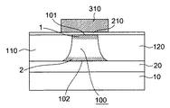
この為に本発明では、図1に1断面例、図2(a)に平面の1例、図2(b)に図2(a)のX−X’線に沿った断面を示すように、
第1の主面101と該第1の主面に対向する第2の主面102を有する半導体薄膜100と、該半導体薄膜第1主面上に設けられた第1のゲート絶縁膜210と、該第1のゲート絶縁膜上に設けられた第1の導電ゲート310と、該第1の導電ゲートを挟んで離間され該第1の導電ゲートから絶縁され前記半導体薄膜100と接して設けられた互いに対向して離間する第1の導電形の第1の半導体領域110と第2の半導体領域120と、前記半導体薄膜と接して設けられ逆導電形の第3の半導体領域130とを有している。
【0010】
さらに、前記半導体薄膜100は第1の導電ゲート下の第1および第2の半導体領域の間で前記第1の主面101と前記第2の主面102間のキャリアが空乏する第1の導電ゲート電位が存在する膜厚と不純物濃度の組み合わせを有している。
【0011】
前記第1の半導体領域と前記第2の半導体領域とで挟まれる前記半導体薄膜部分103と前記逆導電形の第3の半導体領域の間に前記半導体薄膜は延在しており、該半導体薄膜の該延在部分104上に、更に第2のゲート絶縁膜220とその上に設けられた第2の導電ゲート320とを設けたメモリセルを提供する。
【0012】
なお、図2において、421は必要に応じて設けられる第1の導電ゲートと第2の導電ゲートとを絶縁する絶縁膜、400はいわゆるフィールド絶縁膜、
413、431はそれぞれ第3の半導体領域上の絶縁膜、第1の導電ゲート上の絶縁膜、113、123、133、313、323は必要に応じて設けられる第1、第2、第3の半導体領域へのコンタクト、第1、第2導電ゲートへのコンタクトである。また、図1は図2(a)のY−Y’ 線に沿った断面でもある。なお前記コンタクトは必ずしも1セル毎に設ける必要は無い。特に導電ゲートへのコンタクトは、導電ゲートがワード線の1部分を構成することが多いので、多数のセルに1個の割合で必要になるのみである。
【0013】
前記第1の半導体領域110と前記第2の半導体領域120とで挟まれる前記半導体薄膜部分103では第1の導電ゲートのゲート閾値電圧を越える電位によって第1の導電形のチャネルが誘起される。本発明ではこの半導体薄膜部分103を第1のチャネル形成半導体薄膜部分と呼ぶ。
【0014】
前記半導体薄膜の延在部分104では第2の導電ゲートと第3の半導体領域の電位関係により、逆導電形のキャリアが誘起されるないしは逆導電形のキャリア通路が形成される。本発明ではこれを第2のチャネル形成半導体薄膜部分と呼ぶ。この延在部分には逆導電形キャリア通路の第2の導電ゲートからみたゲート閾値電圧調整の為に、104と導電形の異なるまたは不純物濃度の異なる部分105が形成されることもある。なお本発明では前記「ゲート閾値電圧を越える電位」とはnチャネルであればゲート閾値電圧より正方向に大きく、pチャネルであればゲート閾値電圧より負方向に絶対値が大きい事を意味する。
【0015】
本発明では前記第1の主面前記第2の主面間の距離を前記半導体薄膜の厚さと呼ぶ。
【0016】
前記第2の導電ゲートと前記第3の半導体領域との電位関係の第1の組み合わせにより、前記第3の半導体領域から前記第2のチャネル形成半導体薄膜部分を通して第1のチャネル形成半導体薄膜部分へ逆導電形のキャリア2を注入して、前記第1のチャネル形成半導体薄膜部分の前記第1の導電ゲートから見た第1の導電形のチャネルのゲート閾値電圧を第1の値Vth11に変化させる。本発明ではこの動作を「書き込み」と呼ぶ。
【0017】
前記電位関係の第1の組み合わせは、前記第2の導電ゲートの電位から前記第3の半導体領域の電位を引いた値が前記第2の導電ゲートから見た前記第2のチャネル形成半導体薄膜部分の前記第3半導体領域からの逆導電形キャリア通路のゲート閾値電圧Vth2rを越えた値とする。
【0018】
上記第1のチャネル形成半導体薄膜部分に逆導電形のキャリアが注入された状態では第1の導電形のチャネルを誘起する為に必要な第1の導電ゲートに必要なゲート電圧は、前記注入された逆導電形キャリア数または電荷に対応するゲート電圧分だけ少なくて済む。即ち、等価的にゲート閾値電圧がデプレッション側にシフトしたことになる。ゲート閾値電圧がエンハンスメント形の範囲で変化する時は、ゲート閾値電圧の絶対値が減少したことになる。
【0019】
上記第1の電位の組み合わせは、複数のレベルを設定することが出来る。例えば、前記第2の導電ゲートの電位から前記第3の半導体領域の電位を引いた値が前記第2の導電ゲートから見た前記第2のチャネル形成半導体薄膜部分の前記第3半導体領域からの逆導電形キャリア通路のゲート閾値電圧Vth2rを充分越えた値とし、同一ゲート電位に対して第3の半導体領域の電位を複数レベルに設定する。この結果、前記第1の導電ゲートから見た第1の導電形のチャネルの第1のゲート閾値電圧値は複数のレベル(multilevel)Vth11、Vth12、Vth13,…として書き込むことが出来る。即ち、1セル内に複数のビット情報を記憶させることも出来る。
【0020】
第1のチャネル形成半導体薄膜部分へ注入された前記逆導電形のキャリア2は第1の導電形キャリアとの再結合、自己電界による当該第1のチャネル形成半導体薄膜部分からの流出により、徐々に消滅するので、情報の保持のためには消滅する前に前記逆導電形キャリアの第1のチャネル形成半導体薄膜部分での蓄積量を読み出し、それに基づいた再書き込みが必要となる。これを「リフレッシュ」と呼ぶ。
【0021】
前記第2の導電ゲートと前記第3の半導体領域との電位関係の第2の組み合わせにより、第1のチャネル形成半導体薄膜部分から前記第3の半導体領域へ逆導電形のキャリア2を引き出して、前記第1のチャネル形成半導体薄膜部分の前記第1の導電ゲートから見た第1の導電形のチャネルのゲート閾値電圧を第2の値Vth10に変化させる。本発明ではこの動作を「消去」と呼ぶ。
【0022】
前記電位関係の第2の組み合わせは前記第2の導電ゲートの電位から第1のチャネル形成半導体薄膜部分へ注入された逆導電形のキャリアの電位を引いた値が前記第2の導電ゲートから見た前記第2のチャネル形成半導体薄膜部分の逆導電形チャネルのゲート閾値電圧Vth2rを越えた値とする。
【0023】
なお、第1あるいは第2の半導体領域へ逆導電形のキャリアを引き付ける方向の電位(例えば正孔に対しては負方向へ0.6V以上)を与える事で、消去動作を行う事も出来る。この場合、第1の導電形のキャリアも第1のチャネル形成半導体薄膜部分へ供給されるので、再結合により逆導電形のキャリアの消滅が促進される。この消去動作では共通線ないしはビット線に第2の半導体領域ないしは第1の半導体領域が接続されている全セルが消去される。
【0024】
本発明のメモリセルが前記第1のチャネル形成半導体薄膜部分に逆導電形のキャリアを蓄積しているか否かまたはその量の大小により、該メモリセルの記憶情報を判定する。この為には、前記第1の導電ゲートの第2の半導体領域に対する電圧を第1のゲート閾値電圧と第2のゲート閾値電圧のうちすくなくとも1つを越える規定の値に設定して、第1の半導体領域と第2の半導体領域間に流れる電流の大小(「小」はゼロも含む)を検出して記憶情報を判断する。例えば、前記第1の導電ゲートの第2の半導体領域に対する電圧を前記第1のゲート閾値電圧と第2のゲート閾値電圧の間に設定して、第1の半導体領域と第2の半導体領域間に電流が流れるか流れないかを検出して前記記憶情報を判断する。
【0025】
第1のゲート閾値電圧が複数レベルに書き込まれている場合は各レベル間にも第1の導電ゲートの電圧を設定して識別する。または、第1の導電ゲートの第2の半導体領域に対する電圧を前記第1のゲート閾値電圧と第2のゲート閾値電圧のいずれも越える電圧として、第1の半導体領域と第2の半導体領域間に流れる電流の大小で記憶情報を判断する。
【0026】
電流の検出には、参照電流と比較回路で比較検出する場合、ビット線などのキャパシタンスを充電または放電する時定数で検出する場合など公知の手段をとる事が出来る。この動作を「読み出し」と呼ぶ。
【0027】
この読み出し動作で、第1のチャネル形成半導体薄膜部分のエネルギーバンドの価電子帯または伝導帯の電位は逆導電形キャリアを排除する方向へ動く。また第1の導電形のキャリアが多量に第1のチャネル形成半導体薄膜部分に供給されるので、第1のチャネル形成半導体薄膜部分に蓄積されている逆導電形のキャリアとの再結合が加速され、情報が失われる場合がある。この場合は上記リフレッシュ動作を読み出し直後に行わなければならない。
【0028】
なお、図1では半導体薄膜100は絶縁層20を表面に設けた基板10に支持されている。通常基板10はシリコン、絶縁層20はシリコン酸化膜が多い。この表面に絶縁層を設けた支持基板は絶縁基板と呼ばれている。支持基板は石英基板のような全部が絶縁材料でできている絶縁基板も可能となっている。また半導体薄膜の少なくとも一端、または第1の半導体領域ないしは第2の半導体領域ないしは第3の半導体領域の1端が基板に支持された構造でも実施可能である。
【0029】
本発明では書き込み、消去、読み出し時の第1の導電ゲート、第2の導電ゲートの電圧を注意深く選択することにより、各動作モードで同一の電圧とすることも可能であり、この時は図3に例示するように第1および第2の導電ゲートを連続させる、または共有することが出来る。さらにゲート絶縁膜も同一の材料、厚さとする事が出来る。これにより、製造工程数、セル占有面積の減少を図ることができる。この場合は本発明の書き込みおよび消去動作において、「第2の導電ゲート」を「第1の導電ゲート」と読み変えることで書き込みおよび消去動作が実現可能である。
【0030】
本発明では書き込み時に前記第1のゲート閾値電圧値と第2のゲート閾値電圧とに書き分けることも可能である。例えば、前記第2の導電ゲートの電位から前記第3の半導体領域の電位を引いた値が前記第2の導電ゲートから見た前記第2のチャネル形成半導体薄膜部分の前記第3半導体領域からの逆導電形キャリア通路のゲート閾値電圧Vth2rを越えた値とするが、第2の半導体領域の電位に対して第3の半導体領域の電位を順方向へバイアスする場合を第1のゲート閾値電圧書き込みとする。一方、同一の第2のゲート電圧に対して第3の半導体領域の電位をゼロバイアスまたは逆方向へバイアスする場合を第2のゲート閾値電圧書き込み(消去と同じ)とすることが出来る。
【0031】
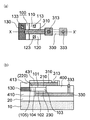
本発明を有効に実施するメモリセルの他の実施形態として、図4に示す様に、
第1の主面101と該第1の主面に対向する第2の主面102を有する半導体薄膜103+104と、該半導体薄膜第1主面上に設けられた第1のゲート絶縁膜210と、該第1ゲート絶縁膜上に設けられた第1の導電ゲート310と、該第1の導電ゲートを挟んで離間され該第1の導電ゲートから絶縁され前記半導体薄膜と接して設けられた互いに対向して離間する第1の導電形の第1の半導体領域110と第2の半導体領域120と、前記半導体薄膜と接して設けられた逆導電形の第3の半導体領域130と、前記第1の半導体領域と前記第2の半導体領域とで挟まれる前記半導体薄膜部分(第1のチャネル形成半導体薄膜部分)103の前記第2の主面に更に設けられた第3のゲート絶縁膜230と該ゲート絶縁膜に接して設けられた第3の導電ゲート330とから少なくとも構成されたことを特徴とするメモリセルが好都合である。なお、半導体薄膜部分104は本発明では第2のチャネル形成半導体薄膜部分とも呼ぶ。
【0032】
第3の導電ゲートからみた第1のチャネル形成半導体薄膜部分の逆導電形キャリア誘起に対するゲート閾値電圧Vth3rを越える電位を該第3の導電ゲートへ与えておけば、逆導電形キャリアは第1のチャネル形成半導体薄膜部分で安定に蓄積される。しかし、消去動作後に、熱励起、キャリアの通常電界におけるわずかな増倍、等により逆導電形キャリアが第1のチャネル形成半導体薄膜部分に徐々に発生して蓄積するので、これを取り去る為のリフレッシュ動作はこの場合も必要となる。
【0033】
図4(a)は前記実施例の薄膜メモリセルの平面図、図4(b)は平面図(a)の鎖線X−X’ に沿った断面図。図において10は支持基板、20は支持基板10表面の絶縁膜、103、104は半導体薄膜100の一部でそれぞれ第1、第2のチャネル形成半導体薄膜部分、210、220は該部分上に設けられたゲート絶縁膜で図では連続して設けられている。310は第1の導電ゲートでこれも第2の導電ゲートと連続して設けられている。110、120はそれぞれ第1、第2の半導体領域、130は第3の半導体領域である。
【0034】
113、123はそれぞれ第1、第2の半導体領域への配線用コンタクト、133は該第3の半導体領域への配線用コンタクト、400は配線等の下に設けられるいわゆるフィールド絶縁膜、431は第1の導電ゲート上に設けられた絶縁膜、410は半導体薄膜100と絶縁膜20の間に設けられた絶縁膜、313は第1の導電ゲートへの配線用コンタクト、333は必要に応じて設けられる第3の導電ゲートへの配線用コンタクトである。
【0035】
なお前記コンタクトは必ずしも1セル毎に設ける必要は無い。特に導電ゲートへのコンタクトは、導電ゲートがワード線の1部分を構成することが多いので、多数のセルに1個の割合で必要になるのみである。不純物領域105も第3の導電ゲートの電界の影響が103の部分より104の部分の方が少なければ(即ち104の部分に図の様にオーバラップしていないか、または230より厚い絶縁膜を介してオーバラップしていれば)必ずしも必要ではない。
【0036】
今まで述べてきた実施形態において、第2のチャネル形成半導体薄膜部分の不純物の導電形、不純物濃度、ないしは第2の導電ゲート材料を第1のチャネル形成半導体薄膜部分の不純物ないしは第1の導電ゲート材料と異ならしめて、それぞれのゲート閾値電圧を異ならしめる事が出来る。特に第3の半導体領域からの逆導電形のキャリア通路にたいする第2の導電ゲートのゲート閾値電圧を第1の導電ゲートのゲート閾値電圧よりエンハンスメント形の方向へ設定することにより、第2のチャネル形成半導体薄膜部分へ注入した逆導電形キャリアが第3の領域へ逆流するのを防ぐ事が出来る。
【0037】
【実施例】
以下、第1の導電形がn形、逆導電形がp形とした場合で動作を説明する。第1の導電形がp形の場合は、符号変化方向が逆になるが原理、効果は変らない。
図5(a)は本発明のセル及びそれを用いたアレイの1実施例の平面図、図5(b)は平面図(a)の鎖線X−X’ に沿った断面図である。
10は支持基板で、この場合はn形シリコン(100)面高抵抗ウエファーである。20は約100nm厚のシリコン酸化膜、103、104、105、110、114、120、124、130、210、220、310、320はそれぞれ本実施例の薄膜メモリセル1000の第1のチャネル形成半導体薄膜部分となる約30nm厚の半導体薄膜、第2のチャネル形成半導体薄膜部分、第2のチャネル形成半導体薄膜部分の高不純物濃度部分、ドレイン(第1の半導体領域)、ドレインエクステンション、ソース(第2の半導体領域)、ソースエクステンション、逆導電形の第3の半導体領域、2.7nm厚の第1のゲート窒化酸化膜、第2のゲート窒化酸化膜、第1の導電ゲートおよびそれと連続した第2の導電ゲートである(300は導電ゲート薄膜としての符号、1001はローカル(部分的な)ワード線としての機能符号。)。
【0038】
210と220は連続している。第1導電ゲートの長さは約100nmであり、本実施例では硼素が添加されたシリコン薄膜で構成される。第1、第2、第3の半導体領域は半導体薄膜の上にエピタキシャル成長した半導体膜も含んで構成されている。第1ないし第2のチャネル形成半導体薄膜部分103,104は隣接するセル間で分離絶縁膜401により分離されている。
【0039】
113は第1の半導体領域へのコンタクトであり、読み出しビット線1005へ接続されている。133は第3の半導体領域へのコンタクトであり、書き込みビット線1004へ接続されている。第1および第2の連続した導電電極310(320)はワード方向へセル間を延在かつ連続して、部分的なワード線1001を形成している。第2の半導体領域はワード方向へセル間を延在して部分的な共通線1003を形成している。部分的なワード線、部分的な共通線は直列抵抗がアレイ動作に影響を及ぼさない範囲の長さまで延在され、選択トランジスタを介すか、あるいは直接グローバルワード線、グローバル共通線へ接続される。上記2種類のビット線も大容量アレイでは選択トランジスタを介してそれぞれの主類のグローバルビット線へ接続される。
【0040】
図5(a)のアレイ配置では、ビット方向に繰り返されるセル1000は互いに鏡像(mirror image)関係に配置されている。この結果、コンタクト113、133はビット方向に隣接するセルと共有している。さらに、第1、3の半導体領域はビット方向の一方に隣接する一方のセルと、第2の半導体領域はビット方向の他方へ隣接する他方のセルと連続している。これによりアレイ面積の縮小を実現している。図5ではセルはワード方向へ2セル、ビット方向へ4セル、合計8セル(1000(j,k)、……、1000(j+1,k+3))分が示されている。このセルの鏡像配置は後述の図8の実施例でも採用されている。
【0041】
以下に本実施例の製造工程を、図6(a)〜(g)、図5(b)の断面図を用いて示す。
(a)高抵抗シリコンウエファーを支持基板10としその上に約100nm厚のシリコン酸化膜20とn形不純物濃度2x10¹⁷原子/cc程度で約35nm厚のシリコン薄膜100を積層したSOI基板を用意する。
(b)このSOI上に熱酸化により約7nmの酸化膜41を成長させ、更に約50nmのシリコン窒化膜42をCVDにより堆積させる。その後、公知のホトリソグラフィによりメモリセルをワード方向、ビット方向に接続した部分、選択トランジスタ部分、周辺回路部分等必要部分のシリコン薄膜を残す為のホトレジストパターン51を形成する。
(c)上記ホトレジストパターン51をマスクとして、対シリコン酸化膜選択比を持ったエッチング条件でシリコン窒化膜をエッチングする。ホトレジストを除去、基板表面をクリーニングして、シリコン窒化膜が除去された部分のシリコン酸化膜露出面に更に約60nmのシリコン酸化膜401が成長するまでパイロジェニック酸化により酸化する。この工程により、上記必要な部分を残してシリコン薄膜100が分離される。
【0042】
このシリコン薄膜の分離は公知のSTI(shallow trench isolation)分離技術を用いても可能である。このシリコン薄膜を平面方向で分離する絶縁膜を絶縁分離膜401とよぶ。
【0043】
熱燐酸系のエッチング液でシリコン窒化膜42を除去し、緩衝弗酸系のエッチング液でシリコン酸化膜41を除去してシリコン薄膜100の表面を露出する。
【0044】
シリコン薄膜100の表面に熱酸化により2.7nm厚のシリコン酸化膜200を形成する。その後、ECR(電子サイクロトロン共鳴:Electron Cyclotron Resonance)、ICP(誘導結合プラズマ:Inductively Coupled Plasma)などの高密度プラズマ装置を用いて、窒素ガス、水素ガス、キセノンガスのプラズマから窒素ラディカルを基板表面へ導き基板温度400℃にて窒化率5〜7%の表面窒化を行う。その後高純度窒素ガス雰囲気搬送を行い800℃窒素中で熱処理を行い、表面欠陥をアニールする。この窒化したシリコン酸化膜が第1及び第2のゲート酸化膜として使われる。
(d)次に導電ゲート薄膜300を堆積する。初期の約10nmは純シリコン薄膜301の堆積を行い、ついで硼素ドープシリコン薄膜302の堆積を約200nm行なう。原料ガスとしてはモノシラン(mono-silane:SiH4)、ジボラン(di-borane:B2H6)を使う。更にその上に約100nmのシリコン窒化膜43を堆積する。上記硼素ドープはイオン注入を用いてもよい。
【0045】
ゲート形状にホトレジストをArFリソグラフィ、電子ビームリソグラフィ等の公知技術により上記シリコン窒化膜/導電ゲート薄膜上にゲート長約100nmのゲート長を有する導電ゲート兼ローカルワード線のパターンを形成し、それをマスクとしてシリコン窒化膜、導電ゲート薄膜の順番にRIE技術によりエッチングを行う。
【0046】
ホトリソグラフィにより形状加工されたホトレジストとシリコン窒化膜/導電ゲート薄膜とを選択マスクとして用いて、それぞれ、n形ドレイン(第1の半導体領域)のエクステンション領域(114)、ソース(第2の半導体領域)のエクステンション領域(124)、を選択的に低加速(砒素約15KeV)イオン注入により形成する。注入ドーズは不純物濃度が約1x1019原子/ccとなる値を選択する(約3x1013原子/cm2)。
【0047】
同様にホトリソグラフィにより形状加工されたホトレジストとシリコン窒化膜/導電ゲート薄膜を選択マスクとして用いて、第3の半導体領域となる部分に選択的に砒素を約8.5x1012原子/cm2 注入する。これにより続く工程で形成される第3の半導体領域に接して第2のチャネル形成半導体薄膜中に高不純物領域105を形成して、第3の半導体領域からの正孔の通路の第2の導電ゲートからみたゲート閾値電圧Vth2rをエンハンスメント側にシフトさせる。
(e)公知のゲートサイドウオール絶縁膜プロセスにより第1、第2導電ゲート薄膜の側面に約30nm厚の絶縁膜サイドウール403を形成する。このサイドウオール作成には約7nm厚のシリコン窒化膜404、約23nm厚のシリコン酸化膜405の2層膜を積層し、この段階ではシリコン窒化膜404は半導体薄膜上には残置する。
【0048】
第3の半導体領域となる部分に開口をもったホトレジストパターンをリソグラフィで作成、該開口部分のシリコン窒化膜404をRIEエッチングする。さらにホトレジストを除去し、開口面に残留しているシリコン酸化膜をウエットエッチし、水素終端処理をする。
【0049】
開口面へ硼素ドープのシリコン結晶膜135を約100nm選択成長する。硼素濃度は約4x10¹⁹ 原子/cc。850℃で熱酸化し、該p形シリコン結晶膜表面、側面へ酸化膜406を約30nm成長させる。この時点で実際はシリコン結晶膜135から硼素が、半導体薄膜100へ拡散して135下の半導体薄膜部分もp形となるが、図6(e)では選択成長したシリコン結晶膜と区別して表す。
(f)メモリセル部分の半導体薄膜100上に残置されているシリコン窒化膜404をRIEエッチングする。さらにエッチ面に残留しているシリコン酸化膜をウエットエッチし、水素終端処理をする。この時半導体領域130となる選択成長した結晶薄膜側面の酸化膜406下の部分のシリコン窒化膜はエッチングされない。
【0050】
開口面へ砒素ドープのシリコン結晶膜115、125を約100nm選択成長する。砒素濃度は5x10²⁰ 原子/cc。前記側面の酸化膜406によりp形高不純物濃度シリコン結晶膜135とn形高不純物濃度シリコン結晶膜115および125は分離される。
【0051】
上記選択結晶成長によらず、ホトレジストパターンと導電ゲート薄膜とその上のシリコン窒化膜をマスクとして選択イオン注入によっても、第1,2,3の半導体領域は形成することが出来る。
【0052】
これら選択結晶成長したシリコン結晶膜から不純物が結晶成長時およびその後の熱工程により半導体薄膜100へその接触部分から拡散して行き、前記選択結晶成長したシリコン結晶薄膜とともに第3の半導体領域130、第1の半導体領域110、第2の半導体領域120を形成する。
(h)導電ゲート薄膜(300)上のシリコン窒化膜43を熱燐酸等でウエットエッチして、洗浄後、ニッケルを約20nm蒸着し、シンターを行い、絶縁膜上の未反応のニッケルを酸でエッチして、ニッケルシリサイド層を残し、更に高温でシンターして第1の半導体領域(ドレイン)上に110s、第2の半導体領域(ソース)上に120s、ゲート薄膜上にシリサイド層300sを形成する。
【0053】
配線用層間絶縁膜440をシリコン酸化膜のCVDにより表面に形成し、必要な部分にコンタクホールを開け、窒化チタン、タングステン等によりコンタクトプラグ133、113を形成、TiNとタングステン薄膜を蒸着、ホトリソグラフィとRIE(reactive ion etching)により配線パターンを形成してローカル書き込みビット線1004、ローカル読み出しビット線1005を得る(図5(b)の状態まで形成される)。さらに必要に応じて層間絶縁膜形成、Al配線、銅配線形成などによる多層配線を形成し、最後にパッシベーション膜を形成する。
【0054】
本実施例では、1)第3の半導体領域と第1の半導体領域が、選択エピタキシャル成長した結晶薄膜側面に設けられた絶縁膜406によって絶縁されていること、2)逆導電形キャリアを誘起するゲート閾値電圧は第1のチャネル形成半導体薄膜部分と第3の半導体領域から第1のチャネル形成半導体薄膜部分へ至る逆導電形キャリアの通路とでは異なること、を特記する。
【0055】
第3の半導体領域から第1のチャネル形成半導体薄膜部分へ至る逆導電形キャリアの通路は第3の半導体領域に接する高不純物濃度領域105をよぎるので、実質的な第2のチャネル形成半導体薄膜部分の不純物濃度はその部分で第1のチャネル形成半導体薄膜部分とは異なる。したがって、逆導電形キャリアを誘起するゲート閾値電圧は第1のチャネル形成半導体薄膜部分と第3の半導体領域から第1のチャネル形成半導体薄膜部分へ至る逆導電形キャリアの通路とでは異なる(上記実施例の場合はエンハンスメント側に約0.5Vシフトしている)。
【0056】
上記のように、第1のチャネル形成半導体薄膜部分と、第3の半導体領域との間に逆導電形キャリアに対するバリアが形成されていると、読み出し時に第1の導電形のキャリアを誘起する方向の電圧が第1の導電ゲートへ加えられても、逆導電形のキャリアが第3の半導体領域へ押し戻される事を一部防ぐので、読み出しにより蓄積情報が消去されるのを防ぐことが出来る。
【0057】
図5の実施例では、縦方向に配置されたセルの第1の半導体領域が読み出しビット線1005へ接続され、第3の半導体領域が書き込みビット線1004へ接続される。横方向へ配置されたセルの第1および第2の共通導電ゲートがワード線1001へ接続される。横方向に配列されたセルの第2の半導体領域は共通線1003へ接続される。読み出しビット線および書き込みビット線は縦方向に延び、ワード線と共通線は横方向へ延びる。セルの配列およびビット線、ワード線の縦横関係は逆になっても問題無い。
【0058】
以下上記実施例により製作された単独セルの動作を述べる。
このセルへの書き込みは、第3の半導体領域の電位に対して第2の導電ゲートに、第2の導電ゲート下の逆導電形キャリア通路の閾値電圧Vthr2 を越える電位関係を与える事で行われる。
【0059】
上記製造工程で作成されたセルでは第2の半導体領域の電位が0Vのとき、Vthr2は約−0.5Vであるので、第3の半導体領域を約0.2〜0.3Vとし、第2導電ゲートは−0.3〜−0.4Vとするのが望ましい。保持状態は第1の導電ゲートは0〜0.2V、第1の半導体領域は第2の半導体領域と同一電位が望ましい。
【0060】
消去は第2の半導体領域を−0.6V以下とするか(第1の半導体領域の電位が0V、第1の導電ゲートが0Vの時)、
第3の半導体領域の電位を0〜−0.4Vとし、第2の導電ゲート電位を−0.55V以下とする。これにより第1のチャネル形成半導体薄膜部分へ蓄積していた逆導電形キャリア(正孔)が第2の領域へ引き抜かれるか、第3の領域へ引き抜かれる。
【0061】
読み出しは、消去されたセルの第1の導電ゲートの第1導電形キャリアのゲート閾値電圧Vth10前後またはそれより0.2V程度まで大きい電圧を第1の導電ゲートへ加えて、第1及び第2の半導体領域間に流れる電流の大小を検出する。多値記憶の場合はVth10、Vth11、Vth12、Vth13、…の間の電圧を第1の導電ゲートへ加えて記憶情報を検出することが出来る。第1と第2の半導体領域間に加える電圧は0.2〜0.9V程度とする。判定基準となる電流は書き込まれたセルと消去されたセルの電流の中間の値を用いる。または、第1の導電ゲートへ各記憶された閾値電圧の間の電圧を加える場合はセル電流の有り無しで情報の判断をする。
【0062】
第1のチャネル形成半導体薄膜部分の高電界領域で、逆極性のキャリアが発生して誤書き込みが起こらないためには第1および第2の半導体領域間の電圧を半導体薄膜のエネルギーギャップの電圧換算値(シリコンの場合は室温で1.1V)以上の電圧を加えない方が安全である。
【0063】
図5に示された本発明のセルを図7に等価回路で示す様に接続したメモリアレイの第1の実施例では下記の表1のような電圧の組み合わせで動作させることが出来る。このアレイは読み出し中に他のワードのセルを書き込めるので特殊用途のメモリとして好都合である。また高速リフレッシュ動作にも適する。表1は1.2Vの単一極性の電源で動作をする場合のワード線、書き込みビット線、読み出しビット線、共通線の電圧関係を示す。単一電源での動作を可能とする為に共通線は正電位、例えば通常0.5Vにバイアスされる。
【0064】
【表1】

【0065】
各線の電位は共通線の電位との差分が表1の関係を保てばよいので、表2の様にも表すことが出来る。
【0066】
【表2】
本発明のメモリセルはアレイ構成として第3の半導体領域と第1の半導体領域とを同じビット線へ接続して(図5のメモリアレイで書き込みビット線と読み出しビット線とを1つのビット線で共通使用)動作させることが出来る。
【0068】
このようなアレイ構成とすることにより、アレイ面積の縮小を計ることが出来る。図8はこのアレイ接続に用いられるメモリセルの平面図で、セル面積は6F2〜4F2とすることが出来る。4F2を実現する為にはセルフアラインコンタクト技術を使用する必要がある。
【0069】
図8のアレイのセルの配置については、図5同様、縦方向は1つおきに第1、第2、第3の半導体領域の導電ゲートに関する上下関係が逆で、かつ上下方向に隣接するセルとそれらの領域を連続させている。たとえば、縦方向k番めのセルは第1、第3の半導体領域をk+1番目のセルと連続させている。第2の半導体領域についてはj番めのセルはj+1番めのセルと連続させている。ワード方向へ隣接するセルの第1の半導体領域は自身と隣接するセルの第3の半導体領域で逆バイアスとわずかな順方向電圧に関しては電気的に分離されている。
【0070】
第1の半導体領域と第3の半導体領域を含むワード方向へ延在する半導体薄膜100は物質的は分離されることなく繋がっている。一方、図5のセルはワード方向へ隣接するセルとは第1の半導体領域は絶縁膜で分離されている例を示しているが、書き込みビット線と読み出しビット線を異なる配線層で構成する等2つのビット線間隔を狭く出来れば、第一の半導体領域側の半導体薄膜も連続させて、第1の半導体領域を第3の半導体領域により電気的に分離する構成を採ることも可能である。
いずれの場合も、ワード方向へ隣接するセル間で第1のチャネル形成半導体薄膜部分ないしは第2のチャネル形成半導体薄膜部分は分離されている。
【0071】
図8の平面図でもセルの第1の導電ゲートと第2の導電ゲートは連続していて、更に横方向へ隣接するセルの第1ないしは第2の導電ゲートと連続している。このゲートは直列抵抗成分を有するので動作速度に限界を与える。これを改善する為には金属配線で主ワード線を構成し、直列抵抗が限界値へ至る前に32〜512個のセル等纏まったセル数毎に導電ゲートと接続することが行われる。
【0072】
図8に示された本発明のセルを図9に等価回路で示す様に接続したメモリアレイの第2の実施例では下記の表3のような電圧の組み合わせで動作させることが出来る。
【0073】
表3は1Vの単一極性の電源で動作をする場合のワード線、ビット線、共通線の電圧関係例を示す。単一電源での動作を可能とする為に共通線は正電位、例えば通常0.3Vにバイアスされる。
【0074】
【表3】
1つの線の電圧は他の線の電圧が標準値の場合は±0.1Vの変動まで許容される。また全部の線の電圧が同じ方向に変化する場合はさらに大きな電位変化が許容される。
【0075】
各線の電位は共通線の電位との差分が表3の関係を保てばよいので、表4の様にも表すことが出来る。
【0076】
【表4】
なお本発明では、半導体薄膜はシリコン単結晶薄膜の他にシリコンゲルマニュウム単結晶薄膜、歪シリコン/シリコンゲルマニュウムの多層膜の場合、ゲート絶縁膜はシリコン酸化膜の他に、シリコン窒化酸化膜、シリコン窒化膜、アルミナ、ハフニュウム酸化膜およびそのシリコン混合物、ジルコニウム酸化物およびそのシリコン混合物等の場合、導電ゲートはポリシリコン以外のシリコンゲルマニウム、タングステン、窒化チタン、チタン/窒化チタン多層膜などの場合、第1、第2,第3の半導体領域が半導体薄膜内部だけでなく、その上に積み上げられている構造の場合、更に金属シリサイドまたは金属薄膜が積層されている場合など、当業者が容易に変形できる範囲で本発明は実施可能である。
【0078】
また第1、第2、第3の半導体領域は半導体薄膜に「接する」と記載されているが、該半導体薄膜中に不純物原子を導入して形成しても、該半導体薄膜上に堆積して形成しても結果として接する状態が形成されていればよい。
【0079】
本発明では第1のチャネル形成半導体薄膜部分へ第2の主面または側面へ容量結合する構造を設けて記憶保持時間、逆導電形キャリア蓄積電荷量の増大を計ることも可能である。
【0080】
【発明の効果】
本発明はPDSOIにも適用することが出来るが、FDSOIに適用してFDSOIでは従来実現が困難であった効果を享受出来る。
【0081】
PDSOIMISだけでなく、FDSOIMIS、FDSONMIS構造でメモリセルとそれを用いたメモリアレイを実現することが出来る。このメモリセルには大きなキャパシタは不要である。
【0082】
このメモリは低電力動作が可能なFDSOIロジックに混載することが可能で、動作電圧も低電力ロジックと共通化可能な範囲にある。
【0083】
さらに、いわゆるニ重ゲートMIS構造でセルを構成することにより、その第3の導電ゲートへ与える電位により、逆導電形キャリアのメモリセルへの蓄積を確実とすることが出来る。
【図面の簡単な説明】
【図1】本発明の原理を示す断面図である。
【図2】本発明の1実施様態を示す平面図(a)、断面図(b)である。
【図3】第1の導電ゲートと第2の導電ゲートが連続した本発明の他の実施様態を示す平面図である。
【図4】半導体薄膜の第2の主面側へ第3の導電ゲートを設けた本発明の他の実施様態を示す平面図(a)、断面図(b)である。
【図5】本発明のメモリセルをアレイ構成に配置、接続した1実施例の平面図(a)、セル部分の断面図(b)である。
【図6】図5に示す実施例のメモリセル及びアレイの製造工程例を示す断面図である。
【図7】図5に示すメモリアレイの等価回路図である。
【図8】書き込みビット線と読み出しビット線を共通としたメモリセルおよびアレイの平面図である。
【図9】図8のメモリアレイの等価回路図である。
【符号の説明】
100 半導体薄膜
101 前記半導体薄膜の第1の主面
102 前記半導体薄膜の第2の主面
1 第1の導電形のキャリア
2 逆導電形のキャリア
10 支持基板
20 支持基板上の絶縁膜
103 第1のチャネル形成半導体薄膜部分
104 第2のチャネル形成半導体薄膜部分
105 第1のチャネル形成半導体薄膜部分と不純物濃度、
不純物の導電形が異なる第2のチャネル形成半導体薄膜
部分
110 第1の半導体領域
120 第2の半導体領域
130 第3の半導体領域
110s、120s、130s シリサイド層
200 ゲート絶縁膜
210 第1のゲート絶縁膜
220 第2のゲート絶縁膜
230 第3のゲート絶縁膜
300 ゲート導電膜
300s シリサイド層
310 第1のゲート導電膜
320 第2のゲート導電膜
330 第3のゲート導電膜
41、400、401、405、406、410、413、431、440 絶縁膜
403 ゲートサイドウオール絶縁膜
42、43、404 シリコン窒化膜
51 ホトレジスト
1000 メモリセル
1001 ワード線
1002 ビット線
1003 共通線
1004 書き込みビット線
1005 読み出しビット線[0001]
BACKGROUND OF THE INVENTION
A technical field having semiconductor memory and its integrated circuits, especially thin film semiconductors such as SOI (Semiconductor On Insulator) and SON (Semiconductor On Nothing) as channel formation regions. When the semiconductor thin film is formed on an insulating substrate (SOI), when both ends are held by the substrate in a hollow state (SON), and when having a protruding shape with one end connected to the substrate Etc.
[0002]
[Prior art]
A proposal to make a dynamic memory without using a capacitor by incorporating two complementary transistors in a partially depleted SOIMOS transistor structure was made in 1993 by H.J.Wann et al. (See, for example, Non-Patent Document 1).
Recently, carriers are generated by using carrier multiplication phenomenon such as avalanche breakdown in the drain high electric field region of partially depleted SOIMOS transistors, and the neutral body is charged by the carriers and flows between the drain and source of the transistor. A memory for reading a change in current has been proposed (see, for example, Non-Patent Document 1).
[0003]
The partially depleted SOI is an SOI having a neutral region in which the depletion layer extends only partially in the thickness direction of the semiconductor thin film, and is abbreviated as PD (Partially Depleted) SOI. The body is a simplified name of the semiconductor thin film in which the channel is formed.
[0004]
[Non-Patent Document 1]
HJWann, C. Hu, “A capacitor-less DRAM cell on SOI substrate”, 1993 IEDM (International Electron Device Meeting) Technical Digest (1993 International Electronic Device) Conference Proceedings), pp.635-638).
[Non-Patent Document 2]
S. Okhonin, et al., “A Capacitor-less 1T-DRAM Cell” (one-transistor dynamic memory without capacitors), IEEE Electron Device Letters, Volume 23, Number 2 (American Institute of Electrical and Electronics Engineers, Electronic Device Letter) 23, No. 2), pp. 85-87, Feb., 2002).
[0005]
[Problems to be solved by the invention]
On the other hand, as low power consumption applications or miniaturization of SOIMOS transistors progresses, SOI becomes fully depleted (FD), and an SOI memory cell applicable to FDSOI is required. Here, FD (Fully Depleted) SOI refers to SOI having such a thickness and impurity concentration that the depletion layer extends over the entire thickness direction of the semiconductor thin film.
[0006]
On the other hand, in the method using carrier multiplication in the drain high electric field portion, weak carrier multiplication also occurs in the non-selected cell connected to the bit line that drives the drain of the writing cell to a high voltage, and so-called write disturb ( It is difficult to form a large array in which a large number of cells are connected per bit line because a weak erroneous writing called “write disturb” occurs.
[0007]
The present invention provides a semiconductor thin film memory cell such as SOI and an array thereof without using a capacitor, which can be applied to FDSOI. Furthermore, the present invention provides a semiconductor thin film memory cell such as SOI, an array thereof, an operating method thereof, and a manufacturing method thereof for a writing or erasing method that does not use carrier multiplication in a drain high electric field portion.
[0008]
[Means for solving the problems]
In the present invention, in order to solve the above-described problems, (1) a method of supplying carriers from a third semiconductor region other than the drain and source to the body without using (2) carrier multiplication in the drain high electric field portion. Take.
[0009]
DETAILED DESCRIPTION OF THE INVENTION
Therefore, in the present invention, as shown in FIG. 1, one cross-sectional example, FIG. 2 (a) shows one example of a plane, and FIG. 2 (b) shows a cross-section along the line XX 'in FIG. 2 (a). ,
A semiconductor thin film having a first
[0010]
Further, the semiconductor thin film100Is a film in which a first conductive gate potential exists in which carriers between the first
[0011]
The semiconductor thin film extends between the semiconductor
[0012]
In FIG. 2,
[0013]
In the semiconductor
[0014]
In the extended
[0015]
In the present invention, the distance between the first main surface and the second main surface is referred to as the thickness of the semiconductor thin film.
[0016]
From the third semiconductor region to the first channel-forming semiconductor thin film portion through the second channel-forming semiconductor thin film portion by the first combination of the potential relationship between the second conductive gate and the third semiconductor region. The reverse
[0017]
The first combination of the potential relations is that the value obtained by subtracting the potential of the third semiconductor region from the potential of the second conductive gate is the second channel forming semiconductor thin film portion viewed from the second conductive gate. A value exceeding the gate threshold voltage Vth2r of the reverse conductivity type carrier path from the third semiconductor region.
[0018]
In the state where carriers of the reverse conductivity type are injected into the first channel forming semiconductor thin film portion, the gate voltage necessary for the first conductive gate necessary for inducing the channel of the first conductivity type is injected. The gate voltage corresponding to the number of reverse conductivity type carriers or electric charge may be reduced. That is, the gate threshold voltage is equivalently shifted to the depletion side. When the gate threshold voltage changes in the enhancement range, the absolute value of the gate threshold voltage is decreased.
[0019]
A plurality of levels can be set for the combination of the first potentials. For example, a value obtained by subtracting the potential of the third semiconductor region from the potential of the second conductive gate is a value obtained from the third semiconductor region of the second channel forming semiconductor thin film portion viewed from the second conductive gate. The gate is set to a value sufficiently exceeding the gate threshold voltage Vth2r of the reverse conductivity type carrier path, and the potential of the third semiconductor region is set to a plurality of levels with respect to the same gate potential. As a result, the first gate threshold voltage value of the channel of the first conductivity type viewed from the first conductive gate can be written as a plurality of levels (multilevel) Vth11, Vth12, Vth13,. That is, a plurality of bit information can be stored in one cell.
[0020]
The reverse
[0021]
With the second combination of the potential relationship between the second conductive gate and the third semiconductor region, the
[0022]
The second combination of the potential relations is that the value obtained by subtracting the potential of the carrier of the opposite conductivity type injected into the first channel forming semiconductor thin film portion from the potential of the second conductive gate is seen from the second conductive gate. Further, it is set to a value exceeding the gate threshold voltage Vth2r of the reverse conductivity type channel of the second channel forming semiconductor thin film portion.
[0023]
Note that an erasing operation can also be performed by applying a potential in a direction that attracts carriers of the opposite conductivity type to the first or second semiconductor region (for example, 0.6 V or more in the negative direction for holes). In this case, since the first conductivity type carrier is also supplied to the first channel forming semiconductor thin film portion, the disappearance of the opposite conductivity type carrier is promoted by recombination. In this erase operation, all cells in which the second semiconductor region or the first semiconductor region is connected to the common line or the bit line are erased.
[0024]
The memory information of the memory cell is determined based on whether or not the memory cell of the present invention stores carriers of the opposite conductivity type in the first channel forming semiconductor thin film portion or the amount thereof. For this purpose, the voltage for the second semiconductor region of the first conductive gate is set to a prescribed value exceeding at least one of the first gate threshold voltage and the second gate threshold voltage, and the first The stored information is determined by detecting the magnitude of the current flowing between the semiconductor region and the second semiconductor region (“small” includes zero). For example, the voltage with respect to the second semiconductor region of the first conductive gate is set between the first gate threshold voltage and the second gate threshold voltage, so that the first semiconductor region and the second semiconductor region are connected. The stored information is determined by detecting whether or not current flows in the memory.
[0025]
When the first gate threshold voltage is written in a plurality of levels, the voltage is identified by setting the voltage of the first conductive gate between the levels. Alternatively, the voltage between the first semiconductor region and the second semiconductor region is set so that the voltage applied to the second semiconductor region of the first conductive gate exceeds the first gate threshold voltage and the second gate threshold voltage. The stored information is judged by the magnitude of the flowing current.
[0026]
For detecting the current, a known means can be used, for example, when comparing and detecting the reference current with a comparison circuit, or when detecting a capacitance such as a bit line with a time constant for charging or discharging. This operation is called “reading”.
[0027]
In this reading operation, the valence band or conduction band potential of the energy band of the first channel-forming semiconductor thin film portion moves in the direction of eliminating the reverse conductivity type carriers. Further, since a large amount of carriers of the first conductivity type are supplied to the first channel forming semiconductor thin film portion, recombination with carriers of the reverse conductivity type accumulated in the first channel forming semiconductor thin film portion is accelerated. Information may be lost. In this case, the refresh operation must be performed immediately after reading.
[0028]
In FIG. 1, the semiconductor thin film100Is supported by a
[0029]
In the present invention, by carefully selecting the voltages of the first conductive gate and the second conductive gate at the time of writing, erasing, and reading, it is possible to make the same voltage in each operation mode. The first and second conductive gates can be continuous or shared as illustrated in FIG. Further, the gate insulating film can be made of the same material and thickness. As a result, the number of manufacturing steps and the cell occupation area can be reduced. In this case, in the write and erase operations of the present invention, the write and erase operations can be realized by changing the “second conductive gate” to the “first conductive gate”.
[0030]
In the present invention, the first gate threshold voltage value and the second gate threshold voltage value can be written separately at the time of writing. For example, a value obtained by subtracting the potential of the third semiconductor region from the potential of the second conductive gate is a value obtained from the third semiconductor region of the second channel forming semiconductor thin film portion viewed from the second conductive gate. When the gate threshold voltage Vth2r of the reverse conductivity type carrier path is exceeded, the first gate threshold voltage is written when the potential of the third semiconductor region is forward biased with respect to the potential of the second semiconductor region. And On the other hand, the case where the potential of the third semiconductor region is biased to zero bias or in the reverse direction with respect to the same second gate voltage can be the second gate threshold voltage writing (same as erasing).
[0031]
As another embodiment of the memory cell for effectively implementing the present invention, as shown in FIG.
A semiconductor
[0032]
If a potential exceeding the gate threshold voltage Vth3r for the reverse conductivity type carrier induction of the first channel forming semiconductor thin film portion viewed from the third conductive gate is given to the third conductive gate, the reverse conductivity type carrier is the first type. Accumulated stably in the channel forming semiconductor thin film portion. However, after the erase operation, the reverse conductivity type carriers are gradually generated and accumulated in the first channel forming semiconductor thin film portion due to thermal excitation, slight multiplication of the carriers in the normal electric field, etc. Action is also required in this case.
[0033]
FIG. 4A is a plan view of the thin film memory cell of the embodiment, and FIG. 4B is a cross-sectional view taken along the chain line X-X ′ in the plan view of FIG. In the figure, 10 is a support substrate, 20 is an insulating film on the surface of the
[0034]
113 and 123 are wiring contacts to the first and second semiconductor regions, 133 is a wiring contact to the third semiconductor region, 400 is a so-called field insulating film provided under the wiring, and 431 is a first insulating film. Insulating film provided on one conductive gate, 410 is a semiconductor thin film100313 is a wiring contact to the first conductive gate, and 333 is a wiring contact to the third conductive gate provided as necessary.
[0035]
The contact is not necessarily provided for each cell. In particular, since the conductive gate often constitutes a part of the word line, the contact to the conductive gate is only required at a rate of one for many cells. In the
[0036]
In the embodiments described so far, the conductivity type, impurity concentration, or second conductive gate material of the second channel forming semiconductor thin film portion is changed to the impurity or first conductive gate of the first channel forming semiconductor thin film portion. Different gate materials can be used for different gate threshold voltages. In particular, the second channel formation is achieved by setting the gate threshold voltage of the second conductive gate for the opposite conductivity type carrier path from the third semiconductor region in an enhancement direction relative to the gate threshold voltage of the first conductive gate. It is possible to prevent reverse conductivity type carriers injected into the semiconductor thin film portion from flowing back to the third region.
[0037]
【Example】
The operation will be described below when the first conductivity type is n-type and the reverse conductivity type is p-type. When the first conductivity type is p-type, the sign change direction is reversed, but the principle and effect are not changed.
FIG. 5A is a plan view of an embodiment of the cell of the present invention and an array using the cell, and FIG. 5B is a cross-sectional view taken along the chain line X-X 'in the plan view of FIG.
[0038]
210 and 220 are continuous. The length of the first conductive gate is about 100 nm, and in this embodiment, the first conductive gate is composed of a silicon thin film to which boron is added. The first, second, and third semiconductor regions include a semiconductor film that is epitaxially grown on the semiconductor thin film. The first and second channel forming semiconductor
[0039]
[0040]
In the array arrangement of FIG. 5A, the
[0041]
The manufacturing process of the present embodiment will be described below using the cross-sectional views of FIGS. 6 (a) to 6 (g) and FIG. 5 (b).
(A) A high-resistance silicon wafer is used as the
(B) An
(C) The above photoresist pattern51Using the mask as a mask, the silicon nitride film is etched under etching conditions having a silicon oxide film selection ratio. The photoresist is removed, the substrate surface is cleaned, and oxidation is performed by pyrogenic oxidation until a
[0042]
This silicon thin film can also be separated using a known STI (shallow trench isolation) separation technique. The insulating film that separates the silicon thin film in the planar direction is called an insulating
[0043]
The
[0044]
A silicon oxide film having a thickness of 2.7 nm is formed on the surface of the silicon
(D) Next, conductive gate thin film300To deposit. In the initial stage, about 10 nm, a pure silicon
[0045]
Form a pattern of a conductive gate and local word line having a gate length of about 100 nm on the silicon nitride film / conductive gate thin film by a known technique such as ArF lithography, electron beam lithography, etc., using a photoresist as a gate shape, and mask it Etching is performed by the RIE technique in the order of the silicon nitride film and the conductive gate thin film.
[0046]
Using the photoresist and the silicon nitride film / conductive gate thin film processed by photolithography as the selection mask, the extension region (114) and the source (second semiconductor region) of the n-type drain (first semiconductor region), respectively. ) Extension regions (124) are selectively formed by low-acceleration (arsenic about 15 KeV) ion implantation. The implantation dose has an impurity concentration of about 1 × 10¹⁹Select a value that will be atoms / cc (about 3x10¹³Atom / cm2).
[0047]
Similarly, using a photoresist and a silicon nitride film / conductive gate thin film processed by photolithography as a selection mask, arsenic is selectively applied to a portion to be the third semiconductor region by about 8.5 × 10 × 10.12Atom / cm2inject. As a result, the
(E) An insulating film side wool having a thickness of about 30 nm on the side surfaces of the first and second conductive gate thin films by a known gate side wall insulating film process.403Form. In order to form the sidewall, a two-layer film of a silicon nitride film 404 having a thickness of about 7 nm and a silicon oxide film 405 having a thickness of about 23 nm is laminated. At this stage, the silicon nitride film 404 is left on the semiconductor thin film.
[0048]
A photoresist pattern having an opening in the portion to be the third semiconductor region is formed by lithography, and the silicon nitride film 404 in the opening is RIE etched. Further, the photoresist is removed, the silicon oxide film remaining on the opening surface is wet-etched, and hydrogen termination is performed.
[0049]
A boron-doped
(F) Semiconductor thin film of memory cell portion100The remaining silicon nitride film 404Etch RIE. Further, the silicon oxide film remaining on the etched surface is wet-etched and subjected to hydrogen termination. At this time, the silicon nitride film under the
[0050]
Arsenic-doped
[0051]
Regardless of the selective crystal growth, the first, second, and third semiconductor regions can also be formed by selective ion implantation using the photoresist pattern, the conductive gate thin film, and the silicon nitride film thereon as a mask.
[0052]
Impurities from these silicon crystals grown by selective crystal are grown in the semiconductor thin film by the thermal process during and after the crystal growth.100The
(H) Conductive gate thin film (300The
[0053]
An interlayer insulating
[0054]
In this embodiment, 1) the third semiconductor region and the first semiconductor region are insulated by an insulating
[0055]
Since the path of the opposite conductivity type carrier from the third semiconductor region to the first channel forming semiconductor thin film portion crosses the high
[0056]
As described above, when the barrier against the reverse conductivity type carrier is formed between the first channel forming semiconductor thin film portion and the third semiconductor region, the direction in which the carrier of the first conductivity type is induced at the time of reading. Even when a voltage of 1 is applied to the first conductive gate, it is possible to prevent some of the reverse conductivity type carriers from being pushed back to the third semiconductor region, so that the stored information can be prevented from being erased by reading.
[0057]
In the embodiment of FIG. 5, the first semiconductor region of the cells arranged in the vertical direction is connected to the read
[0058]
The operation of the single cell manufactured according to the above embodiment will be described below.
Writing to this cell is performed by giving the second conductive gate a potential relationship that exceeds the threshold voltage Vthr2 of the reverse conductivity type carrier path under the second conductive gate with respect to the potential of the third semiconductor region. .
[0059]
In the cell produced in the above manufacturing process, when the potential of the second semiconductor region is 0V, Vthr2 is about -0.5V. Therefore, the third semiconductor region is set to about 0.2 to 0.3V. The conductive gate is preferably -0.3 to -0.4V. In the holding state, the first conductive gate is preferably 0 to 0.2 V, and the first semiconductor region is preferably at the same potential as the second semiconductor region.
[0060]
Erasing is performed by setting the second semiconductor region to −0.6 V or less (when the potential of the first semiconductor region is 0 V and the first conductive gate is 0 V),
The potential of the third semiconductor region is set to 0 to −0.4V, and the second conductive gate potential is set to −0.55V or less. Thereby, the reverse conductivity type carriers (holes) accumulated in the first channel forming semiconductor thin film portion are extracted to the second region or extracted to the third region.
[0061]
In the read operation, a voltage larger than about the gate threshold voltage Vth10 of the first conductivity type carrier of the first conductive gate of the erased cell or about 0.2V higher than that is applied to the first conductive gate, and the first and second The magnitude of the current flowing between the semiconductor regions is detected. In the case of multi-value storage, a voltage between Vth10, Vth11, Vth12, Vth13,... Can be applied to the first conductive gate to detect stored information. The voltage applied between the first and second semiconductor regions is about 0.2 to 0.9V. A current that is a criterion is an intermediate value between currents of written cells and erased cells. Alternatively, when a voltage between the stored threshold voltages is applied to the first conductive gate, information is determined based on the presence or absence of the cell current.
[0062]
In the high electric field region of the first channel forming semiconductor thin film portion, in order to prevent the occurrence of erroneous writing due to the generation of reverse polarity carriers, the voltage between the first and second semiconductor regions is converted to the voltage of the energy gap of the semiconductor thin film. It is safer not to apply a voltage higher than the value (1.1V at room temperature for silicon).
[0063]
In the first embodiment of the memory array in which the cells of the present invention shown in FIG. 5 are connected as shown by the equivalent circuit in FIG. 7, they can be operated with combinations of voltages as shown in Table 1 below. This array is convenient as a special purpose memory because cells of other words can be written during reading. It is also suitable for high-speed refresh operations. Table 1 shows the voltage relationship among the word line, the write bit line, the read bit line, and the common line when operating with a 1.2 V single polarity power supply. In order to allow operation with a single power supply, the common line is biased to a positive potential, typically 0.5V.
[0064]
[Table 1]
[0065]
Since the difference between the potential of each line and the potential of the common line only needs to maintain the relationship shown in Table 1, it can also be expressed as shown in Table 2.
[0066]
[Table 2]
The memory cell of the present invention has an array configuration in which the third semiconductor region and the first semiconductor region are connected to the same bit line (in the memory array of FIG. 5, the write bit line and the read bit line are connected by one bit line). Common use) can be operated.
[0068]
With such an array configuration, the array area can be reduced. FIG. 8 is a plan view of a memory cell used for this array connection, and the cell area is 6F.2~ 4F2It can be. 4F2In order to achieve this, it is necessary to use self-aligned contact technology.
[0069]
As for the arrangement of the cells in the array of FIG. 8, as in FIG. 5, the vertical direction of the conductive gates of the first, second, and third semiconductor regions is opposite every other in the vertical direction, and the cells are adjacent in the vertical direction. And those areas are continuous. For example, the kth cell in the vertical direction has the first and third semiconductor regions connected to the (k + 1) th cell. For the second semiconductor region, the jth cell is continuous with the j + 1st cell. The first semiconductor region of the cell adjacent in the word direction is electrically separated from the third semiconductor region of the cell adjacent to itself in terms of reverse bias and slight forward voltage.
[0070]
Semiconductor thin film extending in the word direction including the first semiconductor region and the third semiconductor region100Are connected without material separation. On the other hand, the cell of FIG. 5 shows an example in which the first semiconductor region is separated from the cell adjacent in the word direction by an insulating film. However, the write bit line and the read bit line are configured by different wiring layers. If the interval between the two bit lines can be narrowed, the semiconductor thin film on the first semiconductor region side can be made continuous so that the first semiconductor region is electrically separated by the third semiconductor region.
In either case, the first channel-forming semiconductor thin film portion or the second channel-forming semiconductor thin film portion is separated between cells adjacent in the word direction.
[0071]
In the plan view of FIG. 8, the first conductive gate and the second conductive gate of the cell are continuous, and further, the first conductive gate and the second conductive gate of the cell adjacent in the lateral direction are continuous. Since this gate has a series resistance component, it limits the operating speed. In order to improve this, the main word line is formed of a metal wiring, and before the series resistance reaches the limit value, it is connected to the conductive gate every 32 to 512 cells or the like.
[0072]
In the second embodiment of the memory array in which the cells of the present invention shown in FIG. 8 are connected as shown by the equivalent circuit in FIG. 9, they can be operated with combinations of voltages as shown in Table 3 below.
[0073]
Table 3 shows an example of a voltage relationship between a word line, a bit line, and a common line when operating with a 1 V single polarity power source. In order to allow operation with a single power supply, the common line is biased to a positive potential, typically 0.3V.
[0074]
[Table 3]
The voltage on one line is allowed up to a variation of ± 0.1V if the voltage on the other line is a standard value. Further, when the voltages of all the lines change in the same direction, a larger potential change is allowed.
[0075]
Since the difference between the potential of each line and the potential of the common line only needs to maintain the relationship shown in Table 3, it can also be expressed as shown in Table 4.
[0076]
[Table 4]
In the present invention, in addition to the silicon single crystal thin film, the semiconductor thin film is a silicon germanium single crystal thin film, and a strained silicon / silicon germanium multilayer film. In addition to the silicon oxide film, the gate insulating film is a silicon oxynitride film, a silicon nitride film. In the case of a film, alumina, hafnium oxide film and its silicon mixture, zirconium oxide and its silicon mixture, etc., the conductive gate is silicon germanium other than polysilicon, tungsten, titanium nitride, titanium / titanium nitride multilayer film, etc. In the case where the second and third semiconductor regions are stacked not only inside the semiconductor thin film but also on the semiconductor thin film, a metal silicide or a metal thin film is further laminated, and the like can be easily modified by those skilled in the art. Thus, the present invention can be implemented.
[0078]
The first, second, and third semiconductor regions are described as “in contact with” the semiconductor thin film. However, even if impurity atoms are introduced into the semiconductor thin film, they are deposited on the semiconductor thin film. Even if it forms, the state which contacts as a result should just be formed.
[0079]
In the present invention, it is also possible to provide a structure for capacitively coupling the first channel forming semiconductor thin film portion to the second main surface or the side surface to increase the memory retention time and the reverse conductivity type carrier accumulated charge amount.
[0080]
【The invention's effect】
The present invention can be applied to PDSOI. However, when the present invention is applied to FDSOI, it is possible to enjoy the effects that have been difficult to realize with FDSOI.
[0081]
In addition to PDSOIMIS, memory cells and memory arrays using the memory cells can be realized with FDSOIMIS and FDSONMIS structures. This memory cell does not require a large capacitor.
[0082]
This memory can be embedded in FDSOI logic capable of low power operation, and the operating voltage is in a range that can be shared with the low power logic.
[0083]
Furthermore, by constituting the cell with a so-called double gate MIS structure, accumulation of reverse conductivity type carriers in the memory cell can be ensured by the potential applied to the third conductive gate.
[Brief description of the drawings]
FIG. 1 is a cross-sectional view showing the principle of the present invention.
FIG. 2 is a plan view (a) and a sectional view (b) showing one embodiment of the present invention.
FIG. 3 is a plan view showing another embodiment of the present invention in which a first conductive gate and a second conductive gate are continuous.
FIGS. 4A and 4B are a plan view and a cross-sectional view showing another embodiment of the present invention in which a third conductive gate is provided on the second main surface side of the semiconductor thin film. FIGS.
FIG. 5A is a plan view of an embodiment in which memory cells of the present invention are arranged and connected in an array configuration, and FIG.
6 is a cross-sectional view showing a manufacturing process example of the memory cell and array of the embodiment shown in FIG. 5;
7 is an equivalent circuit diagram of the memory array shown in FIG. 5. FIG.
FIG. 8 is a plan view of a memory cell and an array having a common write bit line and read bit line.
FIG. 9 is an equivalent circuit diagram of the memory array of FIG. 8;
[Explanation of symbols]
100 Semiconductor thin film
101 First main surface of the semiconductor thin film
102 Second main surface of the semiconductor thin film
1 Carrier of the first conductivity type
2 Carrier of reverse conductivity type
10 Support substrate
20 Insulating film on support substrate
103 1st channel formation semiconductor thin film part
104 Second channel forming semiconductor thin film portion
105 First channel forming semiconductor thin film portion and impurity concentration,
Second channel forming semiconductor thin film with different impurity conductivity types
portion
110 First semiconductor region
120 Second semiconductor region
130 Third semiconductor region
110s, 120s, 130s silicide layers
200 Gate insulation film
210 First gate insulating film
220 Second gate insulating film
230 Third gate insulating film
300 Gate conductive film
300s silicide layer
310 First gate conductive film
320 Second gate conductive film
330 Third gate conductive film
41, 400, 401, 405, 406, 410, 413, 431, 440 Insulating film
403 Gate side wall insulating film
42, 43, 404 Silicon nitride film
51 photoresist
1000 memory cells
1001 Word line
1002 bit line
1003 Common line
1004 Write bit line
1005 Read bit line
Claims (37)
該半導体薄膜の第1の主面上に設けられた第1のゲート絶縁膜と、該第1のゲート絶縁膜上に設けられた第1の導電ゲートと、
該第1の導電ゲートを挟んで離間され、該第1の導電ゲートから絶縁され、前記半導体薄膜と接して設けられた互いに対向して離間する第1の導電形の第1の半導体領域と第2の半導体領域と、
前記半導体薄膜と接して設けられ逆導電形の第3の半導体領域と、
前記第1の半導体領域と前記第2の半導体領域とで挟まれる前記半導体薄膜の部分は第1のチャネル形成半導体薄膜部分を形成し、該部分と前記逆導電形の第3の半導体領域の間に前記半導体薄膜は延在して第2のチャネル形成半導体薄膜部分を形成し、該半導体薄膜の該延在部分上に、更に第2のゲート絶縁膜とその上に設けられた第2の導電ゲートと、
前記第1の導電ゲートと前記第2の導電ゲートとは重畳する部分を有し、該部分で互いを絶縁する絶縁膜と、
を設け、
前記半導体薄膜は前記第1の導電ゲート下の前記第1および前記第2の半導体領域の間で完全空乏形であることを特徴とする薄膜メモリセル。A semiconductor thin film having a first main surface and a second main surface opposite to the first main surface;
A first gate insulating film provided on the first main surface of the semiconductor thin film; a first conductive gate provided on the first gate insulating film;
A first semiconductor region of the first conductivity type spaced apart from and sandwiching the first conductive gate, insulated from the first conductive gate, and in contact with the semiconductor thin film; Two semiconductor regions;
A third semiconductor region of a reverse conductivity type provided in contact with the semiconductor thin film;
The portion of the semiconductor thin film sandwiched between the first semiconductor region and the second semiconductor region forms a first channel-forming semiconductor thin film portion, and between this portion and the third semiconductor region of the opposite conductivity type. The semiconductor thin film extends to form a second channel forming semiconductor thin film portion, and a second gate insulating film and a second conductive film provided thereon are further formed on the extended portion of the semiconductor thin film. The gate,
The first conductive gate and the second conductive gate have an overlapping portion, and an insulating film that insulates the first conductive gate and the second conductive gate;
Provided,
A thin film memory cell, wherein the semiconductor thin film is fully depleted between the first and second semiconductor regions under the first conductive gate.
該半導体薄膜の第1の主面上に設けられた第1のゲート絶縁膜と、該第1のゲート絶縁膜上に設けられた第1の導電ゲートと、
該第1の導電ゲートを挟んで離間され、該第1の導電ゲートから絶縁され、前記半導体薄膜と接して設けられた互いに対向して離間する第1の導電形の第1の半導体領域と第2の半導体領域と、
該第1の半導体領域と第2の半導体領域とが対向する方向とほぼ直交する方向の前記第1の導電ゲート下の一部で前記半導体薄膜と接して設けられ逆導電形の第3の半導体領域とを設け、
前記第1の半導体領域と前記第2の半導体領域とで挟まれる前記半導体薄膜の部分は第1のチャネル形成半導体薄膜部分を形成し、該部分と前記逆導電形の第3の半導体領域の間に至る前記第1のゲート絶縁膜を介した前記第1の導電ゲート下の前記半導体薄膜部分は第2のチャネル形成半導体薄膜部分を形成し、
前記半導体薄膜は前記第1の導電ゲート下の前記第1および前記第2の半導体領域の間で完全空乏形であることを特徴とする薄膜メモリセル。A semiconductor thin film having a first main surface and a second main surface opposite to the first main surface;
A first gate insulating film provided on the first main surface of the semiconductor thin film; a first conductive gate provided on the first gate insulating film;
A first semiconductor region of the first conductivity type spaced apart from and sandwiching the first conductive gate, insulated from the first conductive gate, and in contact with the semiconductor thin film; Two semiconductor regions;
A third semiconductor of reverse conductivity type provided in contact with the semiconductor thin film at a part under the first conductive gate in a direction substantially orthogonal to a direction in which the first semiconductor region and the second semiconductor region face each other. An area and
The portion of the semiconductor thin film sandwiched between the first semiconductor region and the second semiconductor region forms a first channel-forming semiconductor thin film portion, and between this portion and the third semiconductor region of the opposite conductivity type. The semiconductor thin film portion under the first conductive gate through the first gate insulating film leading to a second channel forming semiconductor thin film portion;
A thin film memory cell, wherein the semiconductor thin film is fully depleted between the first and second semiconductor regions under the first conductive gate.
請求項1、2、3、4のいずれか1項記載の複数のメモリセルから構成され、
該複数のワード線の1本と該複数の書き込みビット線の1本と、それと併設された読み出しビット線とが交叉する部分において、
該複数のメモリセルの1つの前記第1及び第2の導電ゲートは該複数のワード線の該1本と接続され、前記第1の半導体領域は該複数の読み出しビット線の該1本と接続され、前記第2の半導体領域は該複数の共通線の1本と接続され、前記第3の半導体領域は該複数の書き込みビット線の該1本と接続されたことを特徴とする薄膜メモリアレイ。A plurality of word lines and a plurality of write bit lines that are insulated and intersected with the plurality of word lines, a plurality of read bit lines provided in parallel therewith, a plurality of common lines,
It is composed of a plurality of memory cells according to any one of claims 1, 2, 3, and 4,
In a portion where one of the plurality of word lines, one of the plurality of write bit lines, and a read bit line provided therewith intersect,
The first and second conductive gates of one of the plurality of memory cells are connected to the one of the plurality of word lines, and the first semiconductor region is connected to the one of the plurality of read bit lines. The thin film memory array, wherein the second semiconductor region is connected to one of the plurality of common lines, and the third semiconductor region is connected to the one of the plurality of write bit lines. .
請求項5、6、7、10、11のいずれか1項記載の複数のメモリセルから構成され、
該複数のワード線の1本と該複数の書き込みビット線の1本と、それと併設された読み出しビット線とが交叉する部分において、
該複数のメモリセルの1つの前記第1の導電ゲートは該複数のワード線の該1本と接続され、前記第1の半導体領域は該複数の読み出しビット線の該1本と接続され、前記第2の半導体領域は該複数の共通線の1本と接続され、前記第3の半導体領域は該複数の書き込みビット線の該1本と接続されたことを特徴とする薄膜メモリアレイ。A plurality of word lines and a plurality of write bit lines that are insulated and intersected with the plurality of word lines, a plurality of read bit lines provided in parallel therewith, a plurality of common lines,
A plurality of memory cells according to any one of claims 5, 6, 7, 10, and 11,
In a portion where one of the plurality of word lines, one of the plurality of write bit lines, and a read bit line provided therewith intersect,
The first conductive gate of one of the plurality of memory cells is connected to the one of the plurality of word lines, the first semiconductor region is connected to the one of the plurality of read bit lines, 2. A thin film memory array, wherein a second semiconductor region is connected to one of the plurality of common lines, and the third semiconductor region is connected to the one of the plurality of write bit lines.
請求項1、2、3、4のいずれか1項記載の複数のメモリセルから構成され、
該複数のワード線の1本と該複数のビット線の1本とが交叉する部分において、
該複数のメモリセルの1つの前記第1及び第2の導電ゲートは該複数のワード線の該1本と接続され、前記第1の半導体領域と第3の半導体領域は該複数のビット線の該1本と接続され、前記第2の半導体領域は該複数の共通線の1本と接続されたことを特徴とする薄膜メモリアレイ。A plurality of word lines, a plurality of bit lines insulated and crossed with each other, a plurality of common lines,
It is composed of a plurality of memory cells according to any one of claims 1, 2, 3, and 4,
In a portion where one of the plurality of word lines and one of the plurality of bit lines intersect,
The first and second conductive gates of one of the plurality of memory cells are connected to the one of the plurality of word lines, and the first semiconductor region and the third semiconductor region are connected to the plurality of bit lines. A thin film memory array, wherein the thin film memory array is connected to the one and the second semiconductor region is connected to one of the plurality of common lines.
請求項5、6、7、10、11のいずれか1項記載の複数のメモリセルから構成され、
該複数のワード線の1本と該複数のビット線の1本とが交叉する部分において、
該複数のメモリセルの1つの前記第1の導電ゲートは該複数のワード線の該1本と接続され、前記第1の半導体領域と第3の半導体領域は該複数のビット線の該1本と接続され、前記第2の半導体領域は該複数の共通線の1本と接続されたことを特徴とする薄膜メモリアレイ。A plurality of word lines, a plurality of bit lines insulated and crossed with each other, a plurality of common lines,
A plurality of memory cells according to any one of claims 5, 6, 7, 10, and 11,
In a portion where one of the plurality of word lines and one of the plurality of bit lines intersect,
The first conductive gate of one of the plurality of memory cells is connected to the one of the plurality of word lines, and the first semiconductor region and the third semiconductor region are the one of the plurality of bit lines. A thin film memory array, wherein the second semiconductor region is connected to one of the plurality of common lines.
前記第3の半導体領域から前記第2のチャネル形成半導体薄膜部分を通して第1のチャネル形成半導体薄膜部分へ逆導電形のキャリアを注入して、前記第1のチャネル形成半導体薄膜部分の前記第1の導電ゲートから見た第1の導電形のチャネルのゲート閾値電圧を第1の値に変化させることを特徴とする請求項1、2、3、4のいずれか1項に記載の薄膜メモリセルの書き込み方法。The value obtained by subtracting the potential of the third semiconductor region from the potential of the second conductive gate is the reverse conductivity from the third semiconductor region of the second channel forming semiconductor thin film portion viewed from the second conductive gate. By setting a value exceeding the gate threshold voltage Vth2r of the shaped carrier path,
Carriers of a reverse conductivity type are injected from the third semiconductor region into the first channel forming semiconductor thin film portion through the second channel forming semiconductor thin film portion, and the first channel forming semiconductor thin film portion has the first 5. The thin film memory cell according to claim 1, wherein the gate threshold voltage of the channel of the first conductivity type viewed from the conductive gate is changed to a first value. Writing method.
前記第3の半導体領域から前記第2のチャネル形成半導体薄膜部分を通して第1のチャ
ネル形成半導体薄膜部分へ逆導電形のキャリアを注入して、前記第1のチャネル形成半導体薄膜部分の前記第1の導電ゲートから見た第1の導電形のチャネルのゲート閾値電圧を第1の値に変化させることを特徴とする請求項5、6、7、10、11のいずれか1項に記載の薄膜メモリセルの書き込み方法。The value obtained by subtracting the potential of the third semiconductor region from the potential of the second conductive gate is the reverse conductivity from the third semiconductor region of the second channel forming semiconductor thin film portion viewed from the second conductive gate. By setting a value exceeding the gate threshold voltage Vth2r of the shaped carrier path,
Carriers of a reverse conductivity type are injected from the third semiconductor region into the first channel forming semiconductor thin film portion through the second channel forming semiconductor thin film portion, and the first channel forming semiconductor thin film portion has the first 12. The thin film memory according to claim 5, wherein a gate threshold voltage of a channel of the first conductivity type as viewed from the conductive gate is changed to a first value. Cell writing method.
の値または前記第2のゲート閾値電圧のうちすくなくとも1つを越える規定の値に設定して、前記第1の半導体領域と前記第2の半導体領域間に流れる電流の大小検出して記憶情報を判断することを特徴とする請求項1、2、3、4、5、6、7、8、9、10、11のいずれか1項に記載の薄膜メモリセルの読み出し方法。The voltage of the first conductive gate with respect to the second semiconductor region is a first value of the gate threshold voltage or a second value of the first gate threshold voltage and the gate threshold voltage.
Or a prescribed value exceeding at least one of the second gate threshold voltages, and detecting the magnitude of the current flowing between the first semiconductor region and the second semiconductor region to detect stored information. The method of reading a thin film memory cell according to any one of claims 1, 2, 3, 4, 5, 6, 7, 8, 9, 10, and 11.
書き込み時はワード線電位が共通線電位−0.4V(±0.1V)、書き込みビット線電位が共通線電位+0.2V(±0.1V)、読み出し線電位が共通線電位であり、
消去時はワード線電位が共通線電位−0.5V(±0.1V)、書き込みビット線電位が共通線電位、読み出しビット線電位が共通線電位であり、
読み出し時はワード線電位が共通線電位+0.7V(±0.1V)、書き込みビット線電位が共通線電位、読み出しビット線電位が共通線電位+0.3V(±0.1V)であることを特徴とする薄膜メモリセルの動作方法。The memory array according to claim 12 or 13,
At the time of writing, the word line potential is the common line potential −0.4 V (± 0.1 V), the write bit line potential is the common line potential +0.2 V (± 0.1 V), and the read line potential is the common line potential.
At the time of erasing, the word line potential is the common line potential -0.5 V (± 0.1 V), the write bit line potential is the common line potential, and the read bit line potential is the common line potential.
When reading, the word line potential is the common line potential +0.7 V (± 0.1 V), the write bit line potential is the common line potential, and the read bit line potential is the common line potential +0.3 V (± 0.1 V). A method of operating a thin film memory cell.
書き込み時はワード線電位が共通線電位−0.3V(±0.1V)、“1”書き込みビット線電位が共通線電位+0.3V(±0.1V)であり、“0”書き込みビット線電位が共通線電位−0.3V(±0.1V)であり、
読み出し時はワード線電位が共通線電位+0.7V(±0.1V)、ビット線電位が共通線電位+0.2V(±0.1V)であることを特徴とする薄膜メモリセルの動作方法。The memory array according to claim 14 or 15,
At the time of writing, the word line potential is the common line potential −0.3 V (± 0.1 V), the “1” write bit line potential is the common line potential +0.3 V (± 0.1 V), and the “0” write bit line The potential is the common line potential -0.3V (± 0.1V),
A method of operating a thin film memory cell, wherein a word line potential is a common line potential +0.7 V (± 0.1 V) and a bit line potential is a common line potential +0.2 V (± 0.1 V) during reading.
第3の半導体領域の該選択結晶成長した部分の少なくとも側面を酸化することと、
第1の半導体領域を選択エピタキシャル成長することと、
を含む請求項1、5、12、13、14、15のいずれか1項に記載の薄膜メモリセルないしは薄膜メモリアレイの製造方法。Selective crystal growth of the third semiconductor region;
Oxidizing at least a side surface of the selectively crystal-grown portion of the third semiconductor region;
Selective epitaxial growth of the first semiconductor region;
16. A method of manufacturing a thin film memory cell or a thin film memory array according to claim 1, comprising:
Priority Applications (8)
| Application Number | Priority Date | Filing Date | Title |
|---|---|---|---|
| JP2003086898A JP4880867B2 (en) | 2002-04-10 | 2003-03-27 | THIN FILM MEMORY, ARRAY, ITS OPERATION METHOD AND MANUFACTURING METHOD |
| TW092107778A TWI264116B (en) | 2002-04-10 | 2003-04-04 | Thin film memory, array, and operation method and manufacture method therefor |
| US10/410,239 US20030213994A1 (en) | 2002-04-10 | 2003-04-09 | Thin film memory, array, and operation method and manufacture method therefor |
| EP03252253A EP1355358B1 (en) | 2002-04-10 | 2003-04-09 | Thin film semiconductor memory and manufacture method therefor |
| EP09166746.9A EP2113943B1 (en) | 2002-04-10 | 2003-04-09 | Thin film memory, array, and operation method and manufacture method therefor |
| CNB031307892A CN100380666C (en) | 2002-04-10 | 2003-04-10 | Thin film memory, array and operating method and producing method thereof |
| KR1020030022660A KR100983408B1 (en) | 2002-04-10 | 2003-04-10 | Thin film memory, array, and operation method and manufacture method therefor |
| US10/879,938 US7211867B2 (en) | 2002-04-10 | 2004-06-28 | Thin film memory, array, and operation method and manufacture method therefor |
Applications Claiming Priority (5)
| Application Number | Priority Date | Filing Date | Title |
|---|---|---|---|
| JP2002108423 | 2002-04-10 | ||
| JP2002108423 | 2002-04-10 | ||
| JP2002230397 | 2002-08-07 | ||
| JP2002230397 | 2002-08-07 | ||
| JP2003086898A JP4880867B2 (en) | 2002-04-10 | 2003-03-27 | THIN FILM MEMORY, ARRAY, ITS OPERATION METHOD AND MANUFACTURING METHOD |
Publications (3)
| Publication Number | Publication Date |
|---|---|
| JP2004128446A JP2004128446A (en) | 2004-04-22 |
| JP2004128446A5 JP2004128446A5 (en) | 2006-05-25 |
| JP4880867B2 true JP4880867B2 (en) | 2012-02-22 |
Family
ID=28678744
Family Applications (1)
| Application Number | Title | Priority Date | Filing Date |
|---|---|---|---|
| JP2003086898A Expired - Fee Related JP4880867B2 (en) | 2002-04-10 | 2003-03-27 | THIN FILM MEMORY, ARRAY, ITS OPERATION METHOD AND MANUFACTURING METHOD |
Country Status (6)
| Country | Link |
|---|---|
| US (2) | US20030213994A1 (en) |
| EP (2) | EP1355358B1 (en) |
| JP (1) | JP4880867B2 (en) |
| KR (1) | KR100983408B1 (en) |
| CN (1) | CN100380666C (en) |
| TW (1) | TWI264116B (en) |
Families Citing this family (65)
| Publication number | Priority date | Publication date | Assignee | Title |
|---|---|---|---|---|
| US20040228168A1 (en) * | 2003-05-13 | 2004-11-18 | Richard Ferrant | Semiconductor memory device and method of operating same |
| US7085153B2 (en) * | 2003-05-13 | 2006-08-01 | Innovative Silicon S.A. | Semiconductor memory cell, array, architecture and device, and method of operating same |
| US7335934B2 (en) * | 2003-07-22 | 2008-02-26 | Innovative Silicon S.A. | Integrated circuit device, and method of fabricating same |
| US7184298B2 (en) * | 2003-09-24 | 2007-02-27 | Innovative Silicon S.A. | Low power programming technique for a floating body memory transistor, memory cell, and memory array |
| US7301803B2 (en) * | 2004-12-22 | 2007-11-27 | Innovative Silicon S.A. | Bipolar reading technique for a memory cell having an electrically floating body transistor |
| FR2880710B1 (en) * | 2005-01-11 | 2007-04-20 | St Microelectronics Sa | METHOD AND DEVICE FOR CHARACTERIZING A CELL INTENDED IN A SILICON-TYPE CMOS TECHNOLOGY ON PARTIALLY DEPLETED INSULATION |
| KR100673228B1 (en) * | 2005-06-30 | 2007-01-22 | 주식회사 하이닉스반도체 | Method of manufacturing a nand flash memory device |
| US20070023833A1 (en) * | 2005-07-28 | 2007-02-01 | Serguei Okhonin | Method for reading a memory cell having an electrically floating body transistor, and memory cell and array implementing same |
| US7606066B2 (en) | 2005-09-07 | 2009-10-20 | Innovative Silicon Isi Sa | Memory cell and memory cell array having an electrically floating body transistor, and methods of operating same |
| US7683430B2 (en) * | 2005-12-19 | 2010-03-23 | Innovative Silicon Isi Sa | Electrically floating body memory cell and array, and method of operating or controlling same |
| US7542345B2 (en) * | 2006-02-16 | 2009-06-02 | Innovative Silicon Isi Sa | Multi-bit memory cell having electrically floating body transistor, and method of programming and reading same |
| US7492632B2 (en) | 2006-04-07 | 2009-02-17 | Innovative Silicon Isi Sa | Memory array having a programmable word length, and method of operating same |
| WO2007128738A1 (en) * | 2006-05-02 | 2007-11-15 | Innovative Silicon Sa | Semiconductor memory cell and array using punch-through to program and read same |
| US8069377B2 (en) * | 2006-06-26 | 2011-11-29 | Micron Technology, Inc. | Integrated circuit having memory array including ECC and column redundancy and method of operating the same |
| US7542340B2 (en) * | 2006-07-11 | 2009-06-02 | Innovative Silicon Isi Sa | Integrated circuit including memory array having a segmented bit line architecture and method of controlling and/or operating same |
| US7893475B2 (en) * | 2007-01-24 | 2011-02-22 | Macronix International Co., Ltd. | Dynamic random access memory cell and manufacturing method thereof |
| KR101277402B1 (en) | 2007-01-26 | 2013-06-20 | 마이크론 테크놀로지, 인코포레이티드 | Floating-body dram transistor comprising source/drain regions separated from the gated body region |
| US7919800B2 (en) | 2007-02-26 | 2011-04-05 | Micron Technology, Inc. | Capacitor-less memory cells and cell arrays |
| WO2009031052A2 (en) * | 2007-03-29 | 2009-03-12 | Innovative Silicon S.A. | Zero-capacitor (floating body) random access memory circuits with polycide word lines and manufacturing methods therefor |
| US8064274B2 (en) | 2007-05-30 | 2011-11-22 | Micron Technology, Inc. | Integrated circuit having voltage generation circuitry for memory cell array, and method of operating and/or controlling same |
| US8085594B2 (en) * | 2007-06-01 | 2011-12-27 | Micron Technology, Inc. | Reading technique for memory cell with electrically floating body transistor |
| WO2009039169A1 (en) | 2007-09-17 | 2009-03-26 | Innovative Silicon S.A. | Refreshing data of memory cells with electrically floating body transistors |
| JP2009088440A (en) * | 2007-10-03 | 2009-04-23 | Oki Semiconductor Co Ltd | Semiconductor device and its manufacturing method |
| US8536628B2 (en) | 2007-11-29 | 2013-09-17 | Micron Technology, Inc. | Integrated circuit having memory cell array including barriers, and method of manufacturing same |
| US8349662B2 (en) * | 2007-12-11 | 2013-01-08 | Micron Technology, Inc. | Integrated circuit having memory cell array, and method of manufacturing same |
| JP2009169071A (en) * | 2008-01-16 | 2009-07-30 | Sony Corp | Display device |
| US8773933B2 (en) | 2012-03-16 | 2014-07-08 | Micron Technology, Inc. | Techniques for accessing memory cells |
| US8014195B2 (en) * | 2008-02-06 | 2011-09-06 | Micron Technology, Inc. | Single transistor memory cell |
| US8189376B2 (en) * | 2008-02-08 | 2012-05-29 | Micron Technology, Inc. | Integrated circuit having memory cells including gate material having high work function, and method of manufacturing same |
| US7957206B2 (en) | 2008-04-04 | 2011-06-07 | Micron Technology, Inc. | Read circuitry for an integrated circuit having memory cells and/or a memory cell array, and method of operating same |
| KR101505494B1 (en) * | 2008-04-30 | 2015-03-24 | 한양대학교 산학협력단 | Cap-less memory device |
| US7947543B2 (en) * | 2008-09-25 | 2011-05-24 | Micron Technology, Inc. | Recessed gate silicon-on-insulator floating body device with self-aligned lateral isolation |
| US7933140B2 (en) | 2008-10-02 | 2011-04-26 | Micron Technology, Inc. | Techniques for reducing a voltage swing |
| US7924630B2 (en) * | 2008-10-15 | 2011-04-12 | Micron Technology, Inc. | Techniques for simultaneously driving a plurality of source lines |
| US8223574B2 (en) * | 2008-11-05 | 2012-07-17 | Micron Technology, Inc. | Techniques for block refreshing a semiconductor memory device |
| KR101570178B1 (en) * | 2008-11-07 | 2015-11-18 | 삼성전자주식회사 | Capacitor-less DRAM device |
| US8213226B2 (en) * | 2008-12-05 | 2012-07-03 | Micron Technology, Inc. | Vertical transistor memory cell and array |
| US8278167B2 (en) * | 2008-12-18 | 2012-10-02 | Micron Technology, Inc. | Method and structure for integrating capacitor-less memory cell with logic |
| US8319294B2 (en) * | 2009-02-18 | 2012-11-27 | Micron Technology, Inc. | Techniques for providing a source line plane |
| US8710566B2 (en) | 2009-03-04 | 2014-04-29 | Micron Technology, Inc. | Techniques for forming a contact to a buried diffusion layer in a semiconductor memory device |
| US8748959B2 (en) * | 2009-03-31 | 2014-06-10 | Micron Technology, Inc. | Semiconductor memory device |
| US8139418B2 (en) * | 2009-04-27 | 2012-03-20 | Micron Technology, Inc. | Techniques for controlling a direct injection semiconductor memory device |
| US8508994B2 (en) | 2009-04-30 | 2013-08-13 | Micron Technology, Inc. | Semiconductor device with floating gate and electrically floating body |
| US8498157B2 (en) * | 2009-05-22 | 2013-07-30 | Micron Technology, Inc. | Techniques for providing a direct injection semiconductor memory device |
| US8537610B2 (en) | 2009-07-10 | 2013-09-17 | Micron Technology, Inc. | Techniques for providing a semiconductor memory device |
| US9076543B2 (en) * | 2009-07-27 | 2015-07-07 | Micron Technology, Inc. | Techniques for providing a direct injection semiconductor memory device |
| US8199595B2 (en) * | 2009-09-04 | 2012-06-12 | Micron Technology, Inc. | Techniques for sensing a semiconductor memory device |
| US8174881B2 (en) | 2009-11-24 | 2012-05-08 | Micron Technology, Inc. | Techniques for reducing disturbance in a semiconductor device |
| US8310893B2 (en) * | 2009-12-16 | 2012-11-13 | Micron Technology, Inc. | Techniques for reducing impact of array disturbs in a semiconductor memory device |
| KR101894400B1 (en) | 2009-12-28 | 2018-09-04 | 가부시키가이샤 한도오따이 에네루기 켄큐쇼 | Memory device and semiconductor device |
| US8416636B2 (en) | 2010-02-12 | 2013-04-09 | Micron Technology, Inc. | Techniques for controlling a semiconductor memory device |
| US8411513B2 (en) * | 2010-03-04 | 2013-04-02 | Micron Technology, Inc. | Techniques for providing a semiconductor memory device having hierarchical bit lines |
| US8576631B2 (en) * | 2010-03-04 | 2013-11-05 | Micron Technology, Inc. | Techniques for sensing a semiconductor memory device |
| US8369177B2 (en) * | 2010-03-05 | 2013-02-05 | Micron Technology, Inc. | Techniques for reading from and/or writing to a semiconductor memory device |
| KR20130007609A (en) | 2010-03-15 | 2013-01-18 | 마이크론 테크놀로지, 인크. | Techniques for providing a semiconductor memory device |
| KR20130007572A (en) | 2010-03-16 | 2013-01-18 | 쌘디스크 3디 엘엘씨 | Bottom electrodes for use with metal oxide resistivity switching layers |
| US8411524B2 (en) | 2010-05-06 | 2013-04-02 | Micron Technology, Inc. | Techniques for refreshing a semiconductor memory device |
| US8841648B2 (en) | 2010-10-14 | 2014-09-23 | Sandisk 3D Llc | Multi-level memory arrays with memory cells that employ bipolar storage elements and methods of forming the same |
| US8389971B2 (en) | 2010-10-14 | 2013-03-05 | Sandisk 3D Llc | Memory cells having storage elements that share material layers with steering elements and methods of forming the same |
| US8531878B2 (en) | 2011-05-17 | 2013-09-10 | Micron Technology, Inc. | Techniques for providing a semiconductor memory device |
| US9559216B2 (en) | 2011-06-06 | 2017-01-31 | Micron Technology, Inc. | Semiconductor memory device and method for biasing same |
| US10037801B2 (en) | 2013-12-06 | 2018-07-31 | Hefei Reliance Memory Limited | 2T-1R architecture for resistive RAM |
| WO2018052760A1 (en) * | 2016-09-13 | 2018-03-22 | Applied Materials, Inc. | Borane mediated dehydrogenation process from silane and alkylsilane species for spacer and hardmask application |
| US11088140B2 (en) * | 2019-08-27 | 2021-08-10 | Nanya Technology Corporation | Multiple semiconductor elements with different threshold voltages |
| US11821936B2 (en) * | 2022-01-10 | 2023-11-21 | Nxp Usa, Inc. | In situ threshold voltage determination of a semiconductor device |
Family Cites Families (15)
| Publication number | Priority date | Publication date | Assignee | Title |
|---|---|---|---|---|
| US4118693A (en) * | 1977-05-09 | 1978-10-03 | Knogo Corporation | Method and apparatus for producing uniform electromagnetic fields in an article detection system |
| JPS586234B2 (en) * | 1977-11-17 | 1983-02-03 | 富士通株式会社 | semiconductor storage device |
| JPS5893370A (en) * | 1981-11-30 | 1983-06-03 | Nec Corp | Mos device |
| JPS6235559A (en) * | 1985-08-09 | 1987-02-16 | Agency Of Ind Science & Technol | Semiconductor memory |
| US5283457A (en) * | 1989-10-02 | 1994-02-01 | Texas Instruments Incorporated | Semiconductor on insulator transistor |
| JPH0799251A (en) * | 1992-12-10 | 1995-04-11 | Sony Corp | Semiconductor memory cell |
| GB9401924D0 (en) * | 1994-02-01 | 1994-03-30 | Jonhig Ltd | System for road toll payment |
| US5784311A (en) * | 1997-06-13 | 1998-07-21 | International Business Machines Corporation | Two-device memory cell on SOI for merged logic and memory applications |
| JPH11224906A (en) * | 1998-02-05 | 1999-08-17 | Sony Corp | Semiconductor memory cell |
| US6225665B1 (en) * | 1999-01-11 | 2001-05-01 | Mitsubishi Denki Kabushiki Kaisha | Semiconductor device having multiple source regions |
| US6111778A (en) * | 1999-05-10 | 2000-08-29 | International Business Machines Corporation | Body contacted dynamic memory |
| TW557569B (en) * | 2000-01-24 | 2003-10-11 | Sony Corp | Semiconductor device and manufacturing method thereof |
| JP3485091B2 (en) * | 2001-01-19 | 2004-01-13 | セイコーエプソン株式会社 | Semiconductor device and manufacturing method thereof |
| US6793127B2 (en) * | 2001-04-04 | 2004-09-21 | Koninklijke Philips Electronics N.V. | Internet enabled resource constrained terminal for processing tags |
| US8321302B2 (en) * | 2002-01-23 | 2012-11-27 | Sensormatic Electronics, LLC | Inventory management system |
-
2003
- 2003-03-27 JP JP2003086898A patent/JP4880867B2/en not_active Expired - Fee Related
- 2003-04-04 TW TW092107778A patent/TWI264116B/en not_active IP Right Cessation
- 2003-04-09 US US10/410,239 patent/US20030213994A1/en not_active Abandoned
- 2003-04-09 EP EP03252253A patent/EP1355358B1/en not_active Expired - Fee Related
- 2003-04-09 EP EP09166746.9A patent/EP2113943B1/en not_active Expired - Fee Related
- 2003-04-10 KR KR1020030022660A patent/KR100983408B1/en active IP Right Grant
- 2003-04-10 CN CNB031307892A patent/CN100380666C/en not_active Expired - Fee Related
-
2004
- 2004-06-28 US US10/879,938 patent/US7211867B2/en active Active
Also Published As
| Publication number | Publication date |
|---|---|
| US20050001269A1 (en) | 2005-01-06 |
| EP1355358B1 (en) | 2013-03-13 |
| US20030213994A1 (en) | 2003-11-20 |
| KR20030081142A (en) | 2003-10-17 |
| EP1355358A3 (en) | 2004-08-04 |
| EP2113943B1 (en) | 2013-07-31 |
| EP2113943A2 (en) | 2009-11-04 |
| CN1453874A (en) | 2003-11-05 |
| KR100983408B1 (en) | 2010-09-20 |
| CN100380666C (en) | 2008-04-09 |
| US7211867B2 (en) | 2007-05-01 |
| TWI264116B (en) | 2006-10-11 |
| EP1355358A2 (en) | 2003-10-22 |
| TW200308082A (en) | 2003-12-16 |
| EP2113943A3 (en) | 2010-10-13 |
| JP2004128446A (en) | 2004-04-22 |
Similar Documents
| Publication | Publication Date | Title |
|---|---|---|
| JP4880867B2 (en) | THIN FILM MEMORY, ARRAY, ITS OPERATION METHOD AND MANUFACTURING METHOD | |
| US11785759B2 (en) | Floating body memory cell having gates favoring different conductivity type regions | |
| JP4927321B2 (en) | Semiconductor memory device | |
| US20160078917A1 (en) | Thyristors, Methods of Programming Thyristors, and Methods of Forming Thyristors | |
| US7432560B2 (en) | Body-tied-to-source MOSFETs with asymmetrical source and drain regions and methods of fabricating the same | |
| US8143656B2 (en) | High performance one-transistor DRAM cell device and manufacturing method thereof | |
| TWI502586B (en) | Memory cells, memory devices and integrated circuits incorporating the same | |
| WO2014185085A1 (en) | Semiconductor storage device | |
| US7894255B1 (en) | Thyristor based memory cell | |
| US7894256B1 (en) | Thyristor based memory cell | |
| US8525248B2 (en) | Memory cell comprising a floating body, a channel region, and a diode | |
| Lin et al. | Performances of a capacitorless 1T-DRAM using polycrystalline silicon thin-film transistors with trenched body | |
| US20220415901A1 (en) | Method for manufacturing memory device using semiconductor element | |
| US20230171944A1 (en) | A Memory Device Comprising an Electrically Floating Body Transistor | |
| US20230145678A1 (en) | Semiconductor memory device and manufacturing method of semiconductor memory device | |
| JPH1140810A (en) | Controllable conduction device |
Legal Events
| Date | Code | Title | Description |
|---|---|---|---|
| A521 | Request for written amendment filed |
Free format text: JAPANESE INTERMEDIATE CODE: A523 Effective date: 20030417 |
|
| A521 | Request for written amendment filed |
Free format text: JAPANESE INTERMEDIATE CODE: A821 Effective date: 20030408 |
|
| RD01 | Notification of change of attorney |
Free format text: JAPANESE INTERMEDIATE CODE: A7421 Effective date: 20040510 |
|
| A521 | Request for written amendment filed |
Free format text: JAPANESE INTERMEDIATE CODE: A523 Effective date: 20040514 |
|
| A621 | Written request for application examination |
Free format text: JAPANESE INTERMEDIATE CODE: A621 Effective date: 20060324 |
|
| A521 | Request for written amendment filed |
Free format text: JAPANESE INTERMEDIATE CODE: A523 Effective date: 20060324 |
|
| RD01 | Notification of change of attorney |
Free format text: JAPANESE INTERMEDIATE CODE: A7421 Effective date: 20100106 |
|
| A131 | Notification of reasons for refusal |
Free format text: JAPANESE INTERMEDIATE CODE: A131 Effective date: 20100223 |
|
| A521 | Request for written amendment filed |
Free format text: JAPANESE INTERMEDIATE CODE: A523 Effective date: 20100416 |
|
| A131 | Notification of reasons for refusal |
Free format text: JAPANESE INTERMEDIATE CODE: A131 Effective date: 20110621 |
|
| A521 | Request for written amendment filed |
Free format text: JAPANESE INTERMEDIATE CODE: A523 Effective date: 20110818 |
|
| A131 | Notification of reasons for refusal |
Free format text: JAPANESE INTERMEDIATE CODE: A131 Effective date: 20110913 |
|
| A521 | Request for written amendment filed |
Free format text: JAPANESE INTERMEDIATE CODE: A523 Effective date: 20111110 |
|
| TRDD | Decision of grant or rejection written | ||
| A01 | Written decision to grant a patent or to grant a registration (utility model) |
Free format text: JAPANESE INTERMEDIATE CODE: A01 Effective date: 20111129 |
|
| A01 | Written decision to grant a patent or to grant a registration (utility model) |
Free format text: JAPANESE INTERMEDIATE CODE: A01 |
|
| A61 | First payment of annual fees (during grant procedure) |
Free format text: JAPANESE INTERMEDIATE CODE: A61 Effective date: 20111202 |
|
| R150 | Certificate of patent or registration of utility model |
Ref document number: 4880867 Country of ref document: JP Free format text: JAPANESE INTERMEDIATE CODE: R150 Free format text: JAPANESE INTERMEDIATE CODE: R150 |
|
| FPAY | Renewal fee payment (event date is renewal date of database) |
Free format text: PAYMENT UNTIL: 20141209 Year of fee payment: 3 |
|
| R250 | Receipt of annual fees |
Free format text: JAPANESE INTERMEDIATE CODE: R250 |
|
| R250 | Receipt of annual fees |
Free format text: JAPANESE INTERMEDIATE CODE: R250 |
|
| S111 | Request for change of ownership or part of ownership |
Free format text: JAPANESE INTERMEDIATE CODE: R313117 |
|
| R350 | Written notification of registration of transfer |
Free format text: JAPANESE INTERMEDIATE CODE: R350 |
|
| R250 | Receipt of annual fees |
Free format text: JAPANESE INTERMEDIATE CODE: R250 |
|
| R250 | Receipt of annual fees |
Free format text: JAPANESE INTERMEDIATE CODE: R250 |
|
| S533 | Written request for registration of change of name |
Free format text: JAPANESE INTERMEDIATE CODE: R313533 |
|
| R350 | Written notification of registration of transfer |
Free format text: JAPANESE INTERMEDIATE CODE: R350 |
|
| R250 | Receipt of annual fees |
Free format text: JAPANESE INTERMEDIATE CODE: R250 |
|
| R250 | Receipt of annual fees |
Free format text: JAPANESE INTERMEDIATE CODE: R250 |
|
| LAPS | Cancellation because of no payment of annual fees |