JP6930911B2 - Integrated device with external light source for molecular search, detection, and analysis - Google Patents
Integrated device with external light source for molecular search, detection, and analysis Download PDFInfo
- Publication number
- JP6930911B2 JP6930911B2 JP2017506981A JP2017506981A JP6930911B2 JP 6930911 B2 JP6930911 B2 JP 6930911B2 JP 2017506981 A JP2017506981 A JP 2017506981A JP 2017506981 A JP2017506981 A JP 2017506981A JP 6930911 B2 JP6930911 B2 JP 6930911B2
- Authority
- JP
- Japan
- Prior art keywords
- waveguide
- excitation
- sample
- excitation energy
- specimen
- Prior art date
- Legal status (The legal status is an assumption and is not a legal conclusion. Google has not performed a legal analysis and makes no representation as to the accuracy of the status listed.)
- Active
Links
Images


Classifications
-
- G—PHYSICS
- G01—MEASURING; TESTING
- G01N—INVESTIGATING OR ANALYSING MATERIALS BY DETERMINING THEIR CHEMICAL OR PHYSICAL PROPERTIES
- G01N21/00—Investigating or analysing materials by the use of optical means, i.e. using sub-millimetre waves, infrared, visible or ultraviolet light
- G01N21/62—Systems in which the material investigated is excited whereby it emits light or causes a change in wavelength of the incident light
- G01N21/63—Systems in which the material investigated is excited whereby it emits light or causes a change in wavelength of the incident light optically excited
- G01N21/64—Fluorescence; Phosphorescence
- G01N21/6408—Fluorescence; Phosphorescence with measurement of decay time, time resolved fluorescence
-
- C—CHEMISTRY; METALLURGY
- C12—BIOCHEMISTRY; BEER; SPIRITS; WINE; VINEGAR; MICROBIOLOGY; ENZYMOLOGY; MUTATION OR GENETIC ENGINEERING
- C12Q—MEASURING OR TESTING PROCESSES INVOLVING ENZYMES, NUCLEIC ACIDS OR MICROORGANISMS; COMPOSITIONS OR TEST PAPERS THEREFOR; PROCESSES OF PREPARING SUCH COMPOSITIONS; CONDITION-RESPONSIVE CONTROL IN MICROBIOLOGICAL OR ENZYMOLOGICAL PROCESSES
- C12Q1/00—Measuring or testing processes involving enzymes, nucleic acids or microorganisms; Compositions therefor; Processes of preparing such compositions
- C12Q1/68—Measuring or testing processes involving enzymes, nucleic acids or microorganisms; Compositions therefor; Processes of preparing such compositions involving nucleic acids
- C12Q1/6869—Methods for sequencing
- C12Q1/6874—Methods for sequencing involving nucleic acid arrays, e.g. sequencing by hybridisation
-
- G—PHYSICS
- G01—MEASURING; TESTING
- G01N—INVESTIGATING OR ANALYSING MATERIALS BY DETERMINING THEIR CHEMICAL OR PHYSICAL PROPERTIES
- G01N21/00—Investigating or analysing materials by the use of optical means, i.e. using sub-millimetre waves, infrared, visible or ultraviolet light
- G01N21/62—Systems in which the material investigated is excited whereby it emits light or causes a change in wavelength of the incident light
- G01N21/63—Systems in which the material investigated is excited whereby it emits light or causes a change in wavelength of the incident light optically excited
- G01N21/64—Fluorescence; Phosphorescence
- G01N21/6428—Measuring fluorescence of fluorescent products of reactions or of fluorochrome labelled reactive substances, e.g. measuring quenching effects, using measuring "optrodes"
-
- G—PHYSICS
- G01—MEASURING; TESTING
- G01N—INVESTIGATING OR ANALYSING MATERIALS BY DETERMINING THEIR CHEMICAL OR PHYSICAL PROPERTIES
- G01N21/00—Investigating or analysing materials by the use of optical means, i.e. using sub-millimetre waves, infrared, visible or ultraviolet light
- G01N21/62—Systems in which the material investigated is excited whereby it emits light or causes a change in wavelength of the incident light
- G01N21/63—Systems in which the material investigated is excited whereby it emits light or causes a change in wavelength of the incident light optically excited
- G01N21/64—Fluorescence; Phosphorescence
- G01N21/645—Specially adapted constructive features of fluorimeters
- G01N21/6452—Individual samples arranged in a regular 2D-array, e.g. multiwell plates
- G01N21/6454—Individual samples arranged in a regular 2D-array, e.g. multiwell plates using an integrated detector array
-
- G—PHYSICS
- G01—MEASURING; TESTING
- G01N—INVESTIGATING OR ANALYSING MATERIALS BY DETERMINING THEIR CHEMICAL OR PHYSICAL PROPERTIES
- G01N21/00—Investigating or analysing materials by the use of optical means, i.e. using sub-millimetre waves, infrared, visible or ultraviolet light
- G01N21/62—Systems in which the material investigated is excited whereby it emits light or causes a change in wavelength of the incident light
- G01N21/63—Systems in which the material investigated is excited whereby it emits light or causes a change in wavelength of the incident light optically excited
- G01N21/64—Fluorescence; Phosphorescence
- G01N21/645—Specially adapted constructive features of fluorimeters
- G01N21/6456—Spatial resolved fluorescence measurements; Imaging
-
- G—PHYSICS
- G01—MEASURING; TESTING
- G01N—INVESTIGATING OR ANALYSING MATERIALS BY DETERMINING THEIR CHEMICAL OR PHYSICAL PROPERTIES
- G01N21/00—Investigating or analysing materials by the use of optical means, i.e. using sub-millimetre waves, infrared, visible or ultraviolet light
- G01N21/62—Systems in which the material investigated is excited whereby it emits light or causes a change in wavelength of the incident light
- G01N21/63—Systems in which the material investigated is excited whereby it emits light or causes a change in wavelength of the incident light optically excited
- G01N21/64—Fluorescence; Phosphorescence
- G01N21/645—Specially adapted constructive features of fluorimeters
- G01N21/648—Specially adapted constructive features of fluorimeters using evanescent coupling or surface plasmon coupling for the excitation of fluorescence
-
- G—PHYSICS
- G01—MEASURING; TESTING
- G01N—INVESTIGATING OR ANALYSING MATERIALS BY DETERMINING THEIR CHEMICAL OR PHYSICAL PROPERTIES
- G01N21/00—Investigating or analysing materials by the use of optical means, i.e. using sub-millimetre waves, infrared, visible or ultraviolet light
- G01N21/62—Systems in which the material investigated is excited whereby it emits light or causes a change in wavelength of the incident light
- G01N21/63—Systems in which the material investigated is excited whereby it emits light or causes a change in wavelength of the incident light optically excited
- G01N21/64—Fluorescence; Phosphorescence
- G01N21/6486—Measuring fluorescence of biological material, e.g. DNA, RNA, cells
-
- G—PHYSICS
- G01—MEASURING; TESTING
- G01N—INVESTIGATING OR ANALYSING MATERIALS BY DETERMINING THEIR CHEMICAL OR PHYSICAL PROPERTIES
- G01N21/00—Investigating or analysing materials by the use of optical means, i.e. using sub-millimetre waves, infrared, visible or ultraviolet light
- G01N21/62—Systems in which the material investigated is excited whereby it emits light or causes a change in wavelength of the incident light
- G01N21/63—Systems in which the material investigated is excited whereby it emits light or causes a change in wavelength of the incident light optically excited
- G01N21/64—Fluorescence; Phosphorescence
- G01N2021/6417—Spectrofluorimetric devices
- G01N2021/6419—Excitation at two or more wavelengths
-
- G—PHYSICS
- G01—MEASURING; TESTING
- G01N—INVESTIGATING OR ANALYSING MATERIALS BY DETERMINING THEIR CHEMICAL OR PHYSICAL PROPERTIES
- G01N21/00—Investigating or analysing materials by the use of optical means, i.e. using sub-millimetre waves, infrared, visible or ultraviolet light
- G01N21/62—Systems in which the material investigated is excited whereby it emits light or causes a change in wavelength of the incident light
- G01N21/63—Systems in which the material investigated is excited whereby it emits light or causes a change in wavelength of the incident light optically excited
- G01N21/64—Fluorescence; Phosphorescence
- G01N2021/6417—Spectrofluorimetric devices
- G01N2021/6421—Measuring at two or more wavelengths
-
- G—PHYSICS
- G01—MEASURING; TESTING
- G01N—INVESTIGATING OR ANALYSING MATERIALS BY DETERMINING THEIR CHEMICAL OR PHYSICAL PROPERTIES
- G01N21/00—Investigating or analysing materials by the use of optical means, i.e. using sub-millimetre waves, infrared, visible or ultraviolet light
- G01N21/62—Systems in which the material investigated is excited whereby it emits light or causes a change in wavelength of the incident light
- G01N21/63—Systems in which the material investigated is excited whereby it emits light or causes a change in wavelength of the incident light optically excited
- G01N21/64—Fluorescence; Phosphorescence
- G01N21/6428—Measuring fluorescence of fluorescent products of reactions or of fluorochrome labelled reactive substances, e.g. measuring quenching effects, using measuring "optrodes"
- G01N2021/6439—Measuring fluorescence of fluorescent products of reactions or of fluorochrome labelled reactive substances, e.g. measuring quenching effects, using measuring "optrodes" with indicators, stains, dyes, tags, labels, marks
- G01N2021/6441—Measuring fluorescence of fluorescent products of reactions or of fluorochrome labelled reactive substances, e.g. measuring quenching effects, using measuring "optrodes" with indicators, stains, dyes, tags, labels, marks with two or more labels
-
- G—PHYSICS
- G01—MEASURING; TESTING
- G01N—INVESTIGATING OR ANALYSING MATERIALS BY DETERMINING THEIR CHEMICAL OR PHYSICAL PROPERTIES
- G01N21/00—Investigating or analysing materials by the use of optical means, i.e. using sub-millimetre waves, infrared, visible or ultraviolet light
- G01N21/62—Systems in which the material investigated is excited whereby it emits light or causes a change in wavelength of the incident light
- G01N21/63—Systems in which the material investigated is excited whereby it emits light or causes a change in wavelength of the incident light optically excited
- G01N21/64—Fluorescence; Phosphorescence
- G01N21/645—Specially adapted constructive features of fluorimeters
- G01N2021/6463—Optics
- G01N2021/6471—Special filters, filter wheel
-
- G—PHYSICS
- G01—MEASURING; TESTING
- G01N—INVESTIGATING OR ANALYSING MATERIALS BY DETERMINING THEIR CHEMICAL OR PHYSICAL PROPERTIES
- G01N2201/00—Features of devices classified in G01N21/00
- G01N2201/06—Illumination; Optics
- G01N2201/064—Stray light conditioning
-
- G—PHYSICS
- G01—MEASURING; TESTING
- G01N—INVESTIGATING OR ANALYSING MATERIALS BY DETERMINING THEIR CHEMICAL OR PHYSICAL PROPERTIES
- G01N2201/00—Features of devices classified in G01N21/00
- G01N2201/06—Illumination; Optics
- G01N2201/069—Supply of sources
- G01N2201/0696—Pulsed
-
- G—PHYSICS
- G01—MEASURING; TESTING
- G01N—INVESTIGATING OR ANALYSING MATERIALS BY DETERMINING THEIR CHEMICAL OR PHYSICAL PROPERTIES
- G01N2201/00—Features of devices classified in G01N21/00
- G01N2201/08—Optical fibres; light guides
-
- G—PHYSICS
- G01—MEASURING; TESTING
- G01N—INVESTIGATING OR ANALYSING MATERIALS BY DETERMINING THEIR CHEMICAL OR PHYSICAL PROPERTIES
- G01N2201/00—Features of devices classified in G01N21/00
- G01N2201/12—Circuits of general importance; Signal processing
Landscapes
- Health & Medical Sciences (AREA)
- Life Sciences & Earth Sciences (AREA)
- Chemical & Material Sciences (AREA)
- Physics & Mathematics (AREA)
- Immunology (AREA)
- Proteomics, Peptides & Aminoacids (AREA)
- Analytical Chemistry (AREA)
- Biochemistry (AREA)
- General Health & Medical Sciences (AREA)
- Organic Chemistry (AREA)
- General Physics & Mathematics (AREA)
- Pathology (AREA)
- Nuclear Medicine, Radiotherapy & Molecular Imaging (AREA)
- Engineering & Computer Science (AREA)
- Zoology (AREA)
- Wood Science & Technology (AREA)
- Molecular Biology (AREA)
- Biotechnology (AREA)
- Microbiology (AREA)
- Biophysics (AREA)
- Bioinformatics & Cheminformatics (AREA)
- General Engineering & Computer Science (AREA)
- Genetics & Genomics (AREA)
- Optics & Photonics (AREA)
- Chemical Kinetics & Catalysis (AREA)
- Biomedical Technology (AREA)
- Investigating, Analyzing Materials By Fluorescence Or Luminescence (AREA)
- Measuring Or Testing Involving Enzymes Or Micro-Organisms (AREA)
- Apparatus Associated With Microorganisms And Enzymes (AREA)
- Optical Measuring Cells (AREA)
- Analysing Materials By The Use Of Radiation (AREA)
Description
本願は、概して、生物および/または化学検体の高速な大規模並列定量解析を実行するための装置、方法、および技術と、前記装置を製造する方法とに関する。 The present application generally relates to devices, methods, and techniques for performing high-speed, large-scale parallel quantitative analysis of biological and / or chemical specimens, and methods of manufacturing said devices.
生物検体の検出および解析は、生物学的アッセイ(「バイオアッセイ」)を使用して実行されることがある。バイオアッセイには従来、大型で高価な研究設備が関わり、研究にあたる科学者は、機器を操作し、バイオアッセイを実行するための訓練を受ける必要がある。さらに、バイオアッセイは従来、大容量で行われ、検出および定量化には特定の種類の検体を大量に要する。 Detection and analysis of biological specimens may be performed using a biological assay (“bioassay”). Bioassays have traditionally involved large and expensive research facilities, requiring research scientists to operate the equipment and be trained to perform bioassays. In addition, bioassays have traditionally been performed in large volumes and require large quantities of certain types of specimens for detection and quantification.
一部のバイオアッセイは、特定の波長の光を放出する発光マーカで検体にタグ付けすることによって行われる。マーカは、光源で照明されて発光させられ、その発光が光検出器により検出されて、マーカにより放出される発光の量が定量化される。発光マーカを用いるバイオアッセイには従来、検体を照明するための高価なレーザ光源と、照明された検体からの発光を収集するための複雑な発光検出光学系および電子機器とが関係する。 Some bioassays are performed by tagging the sample with a luminescent marker that emits light of a particular wavelength. The marker is illuminated by a light source and emitted, and the emission is detected by a photodetector, and the amount of emission emitted by the marker is quantified. Bioassays using luminescence markers have traditionally involved expensive laser sources for illuminating specimens and complex luminescence detection optics and electronics for collecting luminescence from illuminated specimens.
本明細書に記載される技術は、移動コンピューティング機器とインタフェース可能なアクティブソースピクセルの集積装置を使用して、試料を高速解析する装置および方法に関する。集積装置は、少量の試料を受け、試料中の多数の検体の解析を並列して実行するように構成された使い捨てまたはリサイクル可能なラボオンチップ(lab−on−chip)またはパッケージモジュールの形態であってもよい。集積装置は、いくつかの実施形態において、特定の化学物質または生体被験物質の存在を検出し、いくつかの実施形態において化学的または生物学的反応を評価し、いくつかの実施形態において遺伝子配列を判定するために使用されてもよい。いくつかの実施例によれば、集積装置は、単一分子遺伝子配列解析に使用されてもよい。 The techniques described herein relate to devices and methods for high-speed analysis of samples using an integrated device of active source pixels capable of interfacing with mobile computing devices. The accumulator is in the form of a disposable or recyclable lab-on-chip or package module configured to receive a small amount of sample and perform analysis of many samples in parallel in parallel. There may be. The accumulator detects the presence of a particular chemical or biological test substance in some embodiments, evaluates the chemical or biological response in some embodiments, and sequences the gene in some embodiments. May be used to determine. According to some examples, the accumulator may be used for single molecule gene sequence analysis.
いくつかの実施例によれば、使用者は試料を集積装置上のチャンバ内に載せ、集積装置を受容機器内に挿入する。受容機器は、単独でまたはコンピュータと組み合わせて、自動的に集積装置とインタフェースして、集積装置からデータを受け取り、受け取られたデータを処理して、解析結果を使用者に提供する。チップ、受容機器、およびまたはコンピュータ上の積分および演算知能により、使用者に求められる技能レベルが低減されることがわかるであろう。 According to some embodiments, the user places the sample in a chamber on the accumulator and inserts the accumulator into the receiving device. The receiving device, alone or in combination with a computer, automatically interfaces with the accumulator, receives data from the accumulator, processes the received data, and provides the analysis results to the user. It will be found that integral and computational intelligence on chips, receptive devices, and / or computers reduces the skill level required of the user.
本願のいくつかの実施形態によれば、複数のピクセルを含む集積装置が提供される。複数のピクセルのうちのピクセルは、集積装置の外部の励起源から励起エネルギーを受け取るように構成された検体ウェルと、検体ウェル内に位置付けられた検体からの発光を受け取り、かつ受け取られた発光に基づいて検体の識別情報を提供する信号を生成するように位置付けられた少なくとも1つのセンサとを含む。 According to some embodiments of the present application, an integration device including a plurality of pixels is provided. Pixels out of a plurality of pixels receive and receive luminescence from a sample well configured to receive excitation energy from an excitation source outside the integration device and a sample located within the sample well. Includes at least one sensor positioned to generate a signal that provides identification information for the specimen based on it.
いくつかの実施形態において、信号は受け取られた発光の時間的パラメータを示す。いくつかの実施形態において、時間的パラメータは、検体からの発光に関連付けられる寿命である。いくつかの実施形態において、信号は発光のスペクトルを示す。いくつかの実施形態において、信号は発光の特徴的波長を示す。いくつかの実施形態において、信号および励起エネルギーは、検体の吸収スペクトルを示す。いくつかの実施形態において、信号および励起エネルギーは、検体により吸収される特徴的波長を示す。 In some embodiments, the signal indicates a temporal parameter of the received emission. In some embodiments, the temporal parameter is the lifetime associated with luminescence from the specimen. In some embodiments, the signal exhibits a spectrum of emission. In some embodiments, the signal exhibits a characteristic wavelength of emission. In some embodiments, the signal and excitation energies indicate the absorption spectrum of the specimen. In some embodiments, the signal and excitation energy exhibit a characteristic wavelength absorbed by the specimen.
本願のいくつかの実施形態によれば、複数のピクセルを含むピクセル領域を含む集積装置が提供される。複数のピクセルのうちのピクセルは、集積装置の表面上の検体ウェルであって、検体を受けるように構成された検体ウェルと、検体ウェルからの発光を受け取るように構成された少なくとも1つのセンサと、検体ウェルの付近に励起エネルギーを送達する少なくとも1つの導波路とを有する。集積装置は、外部励起エネルギー源から励起エネルギーを受け取り、かつ励起エネルギーを導波路に結合するように構成された結合構成要素を含む励起源結合領域を含む。 According to some embodiments of the present application, an integration device including a pixel region containing a plurality of pixels is provided. A pixel of the plurality of pixels is a sample well on the surface of the accumulator, the sample well configured to receive the sample, and at least one sensor configured to receive light emission from the sample well. The sample well has at least one waveguide for delivering excitation energy. The integration device includes an excitation source coupling region that includes coupling components that receive excitation energy from an external excitation energy source and are configured to couple the excitation energy to the waveguide.
本願のいくつかの実施形態によれば、第一の持続時間を有する励起エネルギーのパルスを放出するように構成された励起源を含む励起源モジュールと、集積装置とを含むシステムが提供される。集積装置は、励起エネルギーのパルスに結合されると発光を放出す検体を受けるように構成された検体ウェルと、第二の持続時間にわり発光を検出するセンサであって、第二の持続時間が第一の持続時間後に発生する、センサと、第一のエネルギー経路であって、それに沿って励起エネルギーのパルスが励起源からエネルギー源結合構成要素へ移動する、第一のエネルギー経路と、第二のエネルギー経路であって、それに沿って励起エネルギーのパルスがエネルギー源結合構成要素から検体ウェルへ移動する、第二のエネルギー経路と、第三のエネルギー経路であって、それに沿って発光が検体ウェルからセンサへ移動する、第三のエネルギー経路とを含む。 According to some embodiments of the present application, there is provided a system comprising an excitation source module comprising an excitation source configured to emit a pulse of excitation energy having a first duration and an integrated device. The integration device is a sample well configured to receive a sample that emits light when coupled to a pulse of excitation energy, and a sensor that detects light emission instead of a second duration, with a second duration. Is generated after the first duration, the sensor and the first energy path, along which the pulse of excitation energy travels from the excitation source to the energy source coupling component, the first energy path and the first. The second energy path, along which the pulse of excitation energy travels from the energy source binding component to the sample well, and the third energy path, along which the luminescence is the sample. Includes a third energy path that travels from the well to the sensor.
本願のいくつかの実施形態によれば、検体における分子の存在を検出する方法が提供される。方法は、複数の発光マーカのうちの1つで標識された検体を検体ウェル内に導入するステップを含み、複数の発光マーカの少なくとも一部は異なる発光寿命値を有する。方法は、検体ウェルに光のパルスを照射するステップと、検体ウェルから放出された光子の到来時間を測定するステップと、光子の到来時間に基づいてマーカの識別を判定するステップとをさらに含む。 According to some embodiments of the present application, there is provided a method of detecting the presence of a molecule in a sample. The method comprises introducing a sample labeled with one of a plurality of luminescence markers into a specimen well, at least a portion of the plurality of luminescence markers having different luminescence lifetime values. The method further comprises irradiating the specimen well with a pulse of light, measuring the arrival time of photons emitted from the specimen well, and determining marker identification based on the arrival time of photons.
本願のいくつかの実施形態によれば、検体ウェルおよびセンサを含む集積装置が提供される。検体ウェルは、複数の発光マーカのうちの1つで標識された検体を受けるように構成され、複数の発光マーカの各々は異なる発光寿命値を有する。センサは、複数の発光マーカのうちの1つからの発光を複数の持続時間にわたって検出するように構成され、複数の持続時間は複数の発光マーカが互いに区別されるように選択される。 According to some embodiments of the present application, an integration device including a sample well and a sensor is provided. The sample well is configured to receive a sample labeled with one of a plurality of luminescence markers, each of the plurality of luminescence markers having a different luminescence lifetime value. The sensor is configured to detect light emission from one of the plurality of emission markers over a plurality of durations, and the plurality of durations are selected so that the plurality of emission markers are distinguished from each other.
本願のいくつかの実施形態によれば、検体ウェルおよび複数のセンサを含む集積装置が提供される。検体ウェルは、複数の発光マーカのうちの1つで標識された検体を受けるように構成される。複数の発光マーカの各々は、複数のスペクトル範囲のうちの1つ内の発光を放出し、および複数のスペクトル範囲のうちの1つで発光を放出する複数の発光マーカの一部はそれぞれ異なる発光寿命値を有する。複数のセンサの各センサは、複数の持続時間にわたって複数のスペクトル範囲のうちの1つを検出するように構成され、複数の持続時間は、複数の発光マーカの一部が互いに区別されるように選択される。 According to some embodiments of the present application, an integration device including a sample well and a plurality of sensors is provided. The specimen well is configured to receive a specimen labeled with one of a plurality of luminescent markers. Each of the plurality of emission markers emits light within one of the plurality of spectral ranges, and some of the plurality of emission markers that emit light within one of the plurality of spectral ranges emit different light. Has a lifetime value. Each sensor of the plurality of sensors is configured to detect one of a plurality of spectral ranges over a plurality of durations so that some of the plurality of emission markers are distinguished from each other. Be selected.
いくつかの実施形態によれば、複数の励起源および集積装置を含むシステムが提供される。複数の励起源は、複数の励起エネルギーを放出するように構成され、複数の励起源の各々は、複数の励起エネルギーのうちの1つのパルスを放出する。集積装置は、複数の発光マーカのうちの1つで標識された検体を受けるように構成された検体ウェルを含む。複数の発光マーカの一部は複数の励起エネルギーのうちの1つにより照明された後に発光を放出し、各々が異なる寿命値を有する。集積装置は、複数の発光マーカのうちの1つからの発光を、複数の励起エネルギーのうちの1つのパルスの後、複数の持続時間にわたって検出するように構成されたセンサをさらに含み、複数の励起エネルギーのうちの1つのパルスのタイミングおよび複数の持続時間によって、複数の発光マーカが互いに区別される
。
According to some embodiments, a system including a plurality of excitation sources and integration devices is provided. The plurality of excitation sources are configured to emit a plurality of excitation energies, and each of the plurality of excitation sources emits a pulse of the plurality of excitation energies. The accumulator includes a sample well configured to receive a sample labeled with one of a plurality of luminescent markers. Some of the plurality of emission markers emit emission after being illuminated by one of the plurality of excitation energies, each having a different lifetime value. The integrated device further includes a plurality of sensors configured to detect light emission from one of the plurality of emission markers over a plurality of durations after one pulse of the plurality of excitation energies. The timing and duration of one of the excitation energies distinguishes the emission markers from each other.
本願のいくつかの実施形態によれば、集積装置を形成する方法が提供される。方法は、複数のセンサ領域を形成するステップであって、複数のセンサ領域のうちの1つのセンサ領域は複数のセンサを含む、ステップと、複数の検体ウェルを形成するステップであって、複数の検体ウェルのうちの1つの検体ウェルは、複数のセンサ領域の対応する1つと整列する、ステップと、複数の検体ウェルから離れて励起エネルギーを結合し、かつ励起エネルギーを少なくとも1つの検体ウェルに誘導するように構成された少なくとも1つの導波路を形成するステップとを含む。 According to some embodiments of the present application, a method of forming an integration device is provided. The method is a step of forming a plurality of sensor regions, wherein one sensor region of the plurality of sensor regions includes a plurality of sensors, and a step of forming a plurality of sample wells. One of the sample wells is aligned with the corresponding one of the multiple sensor regions, the step and the excitation energy are combined away from the plurality of sample wells and the excitation energy is guided to at least one sample well. Includes a step of forming at least one waveguide configured to do so.
本願のいくつかの実施形態によれば、機器が提供される。機器は、少なくとも1つの励起エネルギーを提供する少なくとも1つの励起源と、少なくとも1つの励起源により放出された少なくとも1つの励起エネルギーを集積装置の結合領域に整列させる励起源位置決めシステムと、集積装置上のセンサにより検出された放出エネルギーを表す少なくとも1つの読取り信号を受け取るように構成された読取り回路とを含む。 According to some embodiments of the present application, the device is provided. The instrument comprises at least one excitation source that provides at least one excitation energy and an excitation source positioning system that aligns at least one excitation energy emitted by at least one excitation source to the coupling region of the integration apparatus and on the integration apparatus. Includes a read circuit configured to receive at least one read signal representing the emitted energy detected by the sensor.
本願のいくつかの実施形態によれば、標的核酸分子を配列解析する方法が提供される。方法は、標的核酸分子、重合酵素、および複数の種類のヌクレオチドまたはヌクレオチド類似体を収容する検体ウェルを含む集積装置を提供するステップを含む。複数の種類のヌクレオチドまたはヌクレオチド類似体のうちの各種類のヌクレオチドまたはヌクレオチド類似体は、複数のマーカのうちの1つで標識される。方法は、重合酵素の存在下で標的核酸分子のプライミング位置において伸長反応を実行して、ヌクレオチドまたはヌクレオチド類似体の少なくとも一部を、標的核酸分子と相補的である成長鎖内に連続的に組み込むステップをさらに含み、励起エネルギーによる励起時に、ヌクレオチドまたはヌクレオチド類似体を標識するマーカが、成長鎖内への組込みの際に検体ウェルから放出物を生成し、および放出寿命は複数の種類のヌクレオチドまたはヌクレオチド類似体について区別可能である。方法は、ヌクレオチドまたはヌクレオチド類似体を、放出寿命を示す、センサから受け取られた信号に基づいて識別し、それによって標的核酸分子を配列解析するステップをさらに含む。 According to some embodiments of the present application, a method for sequencing a target nucleic acid molecule is provided. The method comprises providing an accumulator comprising a sample well containing a target nucleic acid molecule, a polymerizable enzyme, and multiple types of nucleotides or nucleotide analogs. Each type of nucleotide or nucleotide analog among the plurality of types of nucleotides or nucleotide analogs is labeled with one of a plurality of markers. The method carries out an extension reaction at the priming position of the target nucleic acid molecule in the presence of a polymerizable enzyme to continuously incorporate at least a portion of the nucleotide or nucleotide analog into the growth chain that is complementary to the target nucleic acid molecule. Markers that further include steps and label nucleotides or nucleotide analogs upon excitation with excitation energy produce emissions from sample wells upon integration into the growth chain, and release lifetimes are multiple types of nucleotides or Nucleotide analogs are distinguishable. The method further comprises identifying nucleotides or nucleotide analogs based on signals received from the sensor indicating the release lifetime, thereby sequencing the target nucleic acid molecule.
本願のいくつかの実施形態によれば、核酸配列解析の方法が提供される。方法は、複数の検体ウェルと、複数の検体ウェルに動作可能に結合された励起エネルギー源とを含む集積装置を提供するステップを含む。複数の検体ウェルの個々の検体ウェルは、標的核酸分子、重合酵素、およびヌクレオチドまたはヌクレオチド類似体を含む。複数のマーカのうちの1つのマーカは、ヌクレオチドまたはヌクレオチド類似体の各々を標識する。方法は、ヌクレオチドまたはヌクレオチド類似体および重合酵素の存在下で標的核酸分子を重合反応に曝して、標的核酸分子と相補的である成長鎖を生成するステップをさらに含む。ヌクレオチドまたはヌクレオチド類似体が成長鎖内に組み込まれている間、複数のマーカは、励起源からの励起エネルギーによる励起時に放出物を放出する。方法は、伸長反応の実行中に放出物の寿命を検出するステップであって、放出の寿命は複数のマーカについて区別可能である、ステップと、標的核酸分子の配列を放出物の寿命に基づいて識別するステップとをさらに含む。 According to some embodiments of the present application, methods of nucleic acid sequence analysis are provided. The method comprises providing an integration device that includes a plurality of sample wells and an excitation energy source operably coupled to the plurality of sample wells. The individual sample wells of the plurality of sample wells contain a target nucleic acid molecule, a polymerizable enzyme, and a nucleotide or nucleotide analog. One of the markers labels each of the nucleotides or nucleotide analogs. The method further comprises exposing the target nucleic acid molecule to a polymerization reaction in the presence of a nucleotide or nucleotide analog and a polymerizable enzyme to produce a growth chain that is complementary to the target nucleic acid molecule. While nucleotides or nucleotide analogs are incorporated within the growth chain, multiple markers emit emissions upon excitation with excitation energy from the excitation source. The method is a step of detecting the lifetime of the release during the execution of the extension reaction, the lifetime of the release being distinguishable for multiple markers, based on the step and the sequence of the target nucleic acid molecule based on the lifetime of the release. It further includes a step of identifying.
本願のいくつかの実施形態によれば、試料を解析する方法が提供される。方法は、複数のピクセルを有する集積装置の表面上に試料を載せるステップであって、各ピクセルは、複数のマーカのうちの第一のマーカで標識された検体を受けるように構成された検体ウェルと、少なくとも1つのセンサを有するセンサ領域とを有する、ステップと、集積装置を、励起エネルギーを第一のピクセルの検体ウェルに結合するための少なくとも1つの励起エネルギー源と、第一のピクセルのセンサ領域の少なくとも1つのセンサからの読取り信号を受け取るための読取り回路とを有する機器と整列させるステップと、第一のマーカを
励起エネルギーで照明するステップと、第一のピクセルのセンサ領域の少なくとも1つのセンサからの読取り信号から、第一のマーカによる放出物から生成された放出エネルギーの寿命を検出するステップとを含む。
According to some embodiments of the present application, a method of analyzing a sample is provided. The method is a step of placing a sample on the surface of a multi-pixel accumulator, each pixel being configured to receive a sample labeled with the first marker of the plurality of markers. And a sensor region having at least one sensor, a step and an integration device, at least one excitation energy source for binding excitation energy to the sample well of the first pixel, and a sensor of the first pixel. A step of aligning with a device having a reading circuit for receiving a read signal from at least one sensor in the region, a step of illuminating the first marker with excitation energy, and at least one of the sensor regions of the first pixel. It includes a step of detecting the lifetime of the emitted energy generated from the emission by the first marker from the read signal from the sensor.
「ピクセル」という用語は、本開示内において、集積装置のユニットセルを指すために使用され得る。ユニットセルは、励起源をさらに含んでいてもよい。ユニットセルは、少なくとも1つの励起結合光学構造(これは、「第一の構造」と呼んでもよい)をさらに含んでいてもよく、これは、励起源から検体ウェルへの励起エネルギーの結合を促進するように構成される。ユニットセルは、少なくとも1つの放出光結合構造をさらに含んでいてもよく、これは、検体ウェルからセンサへの放出物の結合を促進するように構成される。ユニットセルは、集積電子装置(例えば、CMOS装置)をさらに含んでいてもよい。集積装置にアレイ状に配置された複数のピクセルがあってもよい。 The term "pixel" may be used in the present disclosure to refer to a unit cell of an integrated device. The unit cell may further include an excitation source. The unit cell may further comprise at least one excitation-bonded optical structure, which may be referred to as the "first structure", which facilitates the coupling of excitation energy from the excitation source to the sample wells. It is configured to do. The unit cell may further comprise at least one emitted photobinding structure, which is configured to facilitate the binding of the emission from the sample well to the sensor. The unit cell may further include an integrated electronic device (eg, a CMOS device). The integration device may have a plurality of pixels arranged in an array.
「光学」という用語は、本開示において、可視、近赤外、および短波長赤外スペクトルバンドを指すために使用され得る。
「タグ」という用語は、本開示において、タグ、プローブ、またはレポータを指すために使用され得、解析対象の検体に付着されるマーカ、または検体と結合されてもよい反応物質に付着されるマーカを含む。
The term "optics" can be used herein to refer to visible, near-infrared, and short-wave infrared spectral bands.
The term "tag" can be used in the present disclosure to refer to a tag, probe, or reporter, and is attached to a marker that is attached to the sample under analysis, or a marker that is attached to a reactant that may be bound to the sample. including.
「励起エネルギー」という語句は、本開示において、検体ウェル内の検体および/またはマーカに送達されるあらゆる形態のエネルギー(例えば、放射または非放射)を指すために使用され得る。放射励起エネルギーは、1つまたは複数の特徴的波長の光放射を含んでいてもよい。 The phrase "excitation energy" can be used in the present disclosure to refer to any form of energy (eg, radiated or non-radiated) delivered to a sample and / or marker in a sample well. The radiated excitation energy may include synchrotron radiation of one or more characteristic wavelengths.
「特徴的波長」という語句は、本開示において、放射の限定的バンド幅内の中央または支配的波長を指すために使用され得る。場合により、それは放射のバンド幅のピーク波長を指し得る。蛍光体の特徴的波長の例は、563nm、595nm、662nm、および687nmである。 The phrase "characteristic wavelength" may be used in the present disclosure to refer to a central or dominant wavelength within a limited bandwidth of radiation. In some cases, it can refer to the peak wavelength of the radiation bandwidth. Examples of characteristic wavelengths of the phosphor are 563 nm, 595 nm, 662 nm, and 687 nm.
「特徴的エネルギー」という語句は、本開示において、特徴的波長に関連するエネルギーを指すために使用され得る。
「放出物」という用語は、本開示において、マーカおよび/または検体からの発光を指すために使用され得る。これには、放射放出物(例えば、光学放出物)または非放射エネルギー移動(例えば、デクスタ型エネルギー移動またはフェルスタ共鳴エネルギー移動)が含まれる。放出物は、検体ウェル内の検体および/またはマーカの励起から得られる。
The phrase "characteristic energy" may be used in the present disclosure to refer to energy associated with a characteristic wavelength.
The term "emission" can be used in the present disclosure to refer to luminescence from markers and / or specimens. This includes radiant emissions (eg, optical emissions) or non-radiant energy transfers (eg, Dexter-type energy transfers or Ferster resonance energy transfers). The release is obtained from excitation of the specimen and / or marker in the specimen well.
「検体ウェルからの放出物」または「検体からの放出物」という語句は、本開示において、検体ウェル内のマーカおよび/または検体からの放出物を指すために使用され得る。
「セルフアライン」という用語は、本開示において、第一のリソグラフィによるパターニングステップ(例えば、フォトリソグラフィ、イオンビームリソグラフィ、EUVリソグラフィ)によって第一の要素のパターンが印刷され、第二のリソグラフィによるパターニングステップによって、第一のリソグラフィによるパターニングステップと整合させて第二の要素のパターンが印刷される2つの別々のリソグラフィパターニングステップを使用せずに、少なくとも2つの異なる要素(例えば、検体ウェルおよび放出物結合構造、検体ウェルおよび励起源)が製造されて、相互に整列される微細製作プロセスを指すために使用され得る。セルフアラインプロセスは、1つのリソグラフィパターニングステップに第一および第二の要素の両方のパターンを含めるステップを含んでいてもよく、または第一の要素の製造後の構造の特徴物を使用して第二の要素を形成するステップを含んでいてもよい。
The phrase "emission from a specimen well" or "emission from a specimen" can be used in the present disclosure to refer to markers and / or emissions from a specimen in a specimen well.
The term "self-alignment" is used herein to print a pattern of a first element by a patterning step by first lithography (eg, photolithography, ion beam lithography, EUV lithography) and a patterning step by second lithography. At least two different elements (eg, specimen wells and discharge binding) without the use of two separate lithographic patterning steps in which the pattern of the second element is printed in line with the patterning step by the first lithography. Structures, specimen wells and excitation sources) can be manufactured and used to refer to a microfabrication process that is aligned with each other. The self-aligning process may include the step of including both the patterns of the first and second elements in one lithography patterning step, or the first element using post-manufacturing structural features of the first element. It may include steps to form the second element.
「センサ」という用語は、本開示において、検体ウェルからの放出物を検出して、検出された放出物を表す少なくとも1つの電気信号を生成するように構成された1つまたは複数の集積回路装置を指すために使用され得る。 The term "sensor" is used herein to detect one or more integrated circuit devices configured to detect emissions from sample wells and generate at least one electrical signal representing the detected emissions. Can be used to point to.
「ナノスケール」という用語は、本開示において、その少なくとも1つの寸法または最小特徴物の大きさが150ナノメートル(nm:nanometer)以下であり、約500nmを超えないオーダである構造を指すために使用され得る。 The term "nanoscale" is used herein to refer to a structure in which at least one dimension or minimum feature size is 150 nanometers (nm: nanometer) or less and is on the order not to exceed about 500 nm. Can be used.
「マイクロスケール」という用語は、本開示において、その少なくとも1つの寸法または最小構造物の大きさが約500nm〜約100マイクロメートルである構造を指すために使用され得る。 The term "microscale" can be used in the present disclosure to refer to a structure in which at least one dimension or size of the smallest structure is from about 500 nm to about 100 micrometers.
「励起エネルギーを増大させる」という語句は、本開示において、検体ウェルの励起領域における励起エネルギーの強度を高めることを指すために使用され得る。強度は、例えば検体ウェルに入射する励起エネルギーを集束および/または共振させることによって高められてもよい。場合により、強度は、励起エネルギーが検体ウェルの励起領域内にさらに浸透できるようにする反射防止コーティングまたは損失層によって高められてもよい。励起エネルギーの増大は、検体ウェルの励起領域における励起エネルギーを増大させるための構造を含まない実施形態の比較基準であってもよい。 The phrase "increasing excitation energy" can be used herein to refer to increasing the intensity of excitation energy in the excitation region of a sample well. The intensity may be increased, for example, by focusing and / or resonating the excitation energy incident on the specimen well. Optionally, the intensity may be enhanced by an antireflection coating or loss layer that allows the excitation energy to penetrate further into the excitation region of the specimen well. The increase in excitation energy may be a comparative criterion of an embodiment that does not include a structure for increasing the excitation energy in the excitation region of the sample well.
「約」、「略」、「実質的に」という用語は、本開示において、数値を示すために使用され得、言及された数値プラスおよびマイナス容認可能なばらつきの範囲を含むものとする。ばらつきの大きさは、ある実施形態では5%未満、ある実施形態では10%未満、さらにある実施形態では20%未満とすることができる。装置が広い数値範囲、例えば1桁以上の範囲で適正に機能できる実施形態において、ばらつきの量は係数2とすることができる。例えば、装置が20〜350の範囲の数値で適正に機能する場合、「約80」は40〜160の数値を含んでいてもよい。 The terms "about," "abbreviation," and "substantially" are used herein to indicate numerical values and include the range of positive and negative acceptable variability referred to. The magnitude of the variability can be less than 5% in some embodiments, less than 10% in some embodiments, and less than 20% in some embodiments. In embodiments where the device can function properly in a wide numerical range, eg, a range of one digit or more, the amount of variation can be a factor of 2. For example, "about 80" may include a number from 40 to 160 if the device functions properly with a number in the range of 20 to 350.
「隣接」という用語は、本開示において、相互に近接して(例えば、ピクセルの横または縦寸法の約5分の1未満の距離内に)配置された2つの要素を指すために使用され得る。場合により、隣接する要素間に介在構造または層があってもよい。場合により、隣接する要素は、介在する構造または要素がない状態で相互に直接隣接していてもよい。 The term "adjacent" can be used in the present disclosure to refer to two elements that are located in close proximity to each other (eg, within a distance of less than about one-fifth the horizontal or vertical dimension of a pixel). .. Optionally, there may be intervening structures or layers between adjacent elements. In some cases, adjacent elements may be directly adjacent to each other in the absence of intervening structures or elements.
「検出」という用語は、本開示において、センサにおいて検体ウェルから放出物を受け、その放出物を表すか、またはそれに関連する少なくとも1つの電気信号を生成することを指すために使用され得る。「検出」という用語はまた、本開示において、検体ウェルからの放出物に基づいて、検体ウェル内の特定の検体またはマーカの存在を判定するか、またはその特性を識別することを指すために使用され得る。 The term "detection" can be used in the present disclosure to refer to receiving an emission from a specimen well in a sensor to represent or generate at least one electrical signal associated therewith. The term "detection" is also used herein to refer to determining the presence of a particular sample or marker in a sample well or identifying its properties based on emissions from the sample well. Can be done.
本教示の上述のおよびその他の態様、実施形態、および特徴は、添付の図面と共に以下の説明を読むことでよりよく理解できる。
当業者であれば、本明細書中で説明する図面が例示を目的としているにすぎないことがわかるであろう。当然のことながら、いくつかの例において、本発明の各種の態様が本発明の理解を容易にするために誇張または拡大して示され得る。図面中、同様の参照文字は異なる図面を通じて概して同様の特徴、機能的に同様のおよび/または構造的に同様の要素を指す。図面は必ずしも正確な縮尺によるとはかぎらず、その代わりに本教示の原理を例示することに重点を置いている。図面は、決して本教示の範囲を限定することを意図されていない。
The above and other aspects, embodiments, and features of this teaching can be better understood by reading the following description along with the accompanying drawings.
Those skilled in the art will appreciate that the drawings described herein are for illustration purposes only. Of course, in some examples, various aspects of the invention may be exaggerated or expanded to facilitate understanding of the invention. In drawings, similar reference characters generally refer to similar features, functionally similar and / or structurally similar elements throughout different drawings. The drawings are not necessarily at exact scale and instead focus on exemplifying the principles of this teaching. The drawings are by no means intended to limit the scope of this teaching.
本発明の特徴および利点は、後述の詳細な説明を添付の図面と併せて読むことにより、
より明らかとなるであろう。
図面に関して実施形態を説明する際、方向に関する言及(「上」、「下」、「上側」、「下側」、「左」、「右」、「水平」、「垂直」等)が使用され得る。このような言及は、通常の向きで図面を見ている読者にとっての補助となるためのものにすぎない。これらの方向に関する言及は、実施される装置の好ましいまたは唯一の向きを説明しようとするものではない。装置は他の向きでも実施されてよい。
The features and advantages of the present invention can be described by reading the detailed description below in conjunction with the accompanying drawings.
It will be more obvious.
When describing embodiments with respect to drawings, directional references (“top”, “bottom”, “top”, “bottom”, “left”, “right”, “horizontal”, “vertical”, etc.) are used. obtain. Such references are only to assist the reader looking at the drawing in the normal orientation. References to these orientations are not intended to explain the preferred or unique orientation of the device being implemented. The device may be implemented in other orientations.
本発明者らは、単一分子または粒子の検出および定量化を実行するための小型の高速装置により、生物および/または化学試料の複雑な定量的測定の実行コストを削減でき、生化学的な技術的発見速度を急速に高められることを認識し、そのように理解した。さらに、容易に持ち運び可能な費用対効果の高い装置は、先進諸国で行われているバイオアッセイの方法を変化させるだけでなく、発展途上国の人々に対して初めて重要な診断試験を利用できるようにし、これは、発展途上国の人々の健康および福利を劇的に改善し得る。例えば、本明細書に記載されている実施形態は、個人が家庭で、または医師が発展途上国の遠隔の診療所で使用できる、血液、尿、および/または唾液の診断試験に使用されてもよい。 We can reduce the cost of performing complex quantitative measurements of biological and / or chemical samples with a small, high-speed device for performing detection and quantification of single molecules or particles, biochemically. We recognized and understood that the speed of technical discovery could be increased rapidly. In addition, an easily portable and cost-effective device will not only change the way bioassays are performed in developed countries, but will also make important diagnostic tests available to people in developing countries for the first time. This can dramatically improve the health and well-being of people in developing countries. For example, the embodiments described herein may be used in blood, urine, and / or saliva diagnostic tests that can be used by individuals at home or by physicians in remote clinics in developing countries. good.
多数のピクセル(例えば、数百数千、数百万またはそれを超える)を有するピクセル化されたセンサ装置によって、複数の個別の分子または粒子の並列検出が可能となる。分子は、例えばタンパク質および/またはDNAであってもよいが、これらに限定されない。さらに、1秒間に100フレームを超えるデータ取得が可能な高速装置により、解析中の検体内で時間が経つと生じるダイナミックプロセスまたは変化の検出および解析が可能となる。 Pixelized sensor devices with a large number of pixels (eg, hundreds, thousands, millions or more) allow parallel detection of multiple individual molecules or particles. Molecules may be, for example, proteins and / or DNA, but are not limited thereto. In addition, a high-speed device capable of acquiring more than 100 frames per second enables detection and analysis of dynamic processes or changes that occur over time in the sample being analyzed.
本発明者らは、バイオアッセイ機器の小型化を妨げている1つのハードルが、励起光をフィルタにかけ、センサにおける望ましくない検出イベントを引き起こさないようにする必要性であったことを認識し、そのように理解した。所望の信号光(発光)を透過させ、励起光を十分に遮断するために使用される光学フィルタは、厚く、嵩張り、高価で、光の入射角度のばらつきの影響を受けやすいことがあり得るため、小型化を阻んでいる。しかしながら、本発明者らは、パルス式励起源を使用すれば、このようなフィルタ処理に対する必要性を低減化でき、または場合により、このようなフィルタも不要となることを認識し、そのように理解した。励起光パルスに関して光子が検出された時間を判定できるセンサを使用することにより、受け取られた光のスペクトルではなく、光子が受け取られた時間に基づいて信号光を励起光から分離できる。したがって、いくつかの実施形態において、嵩張る光学フィルタの必要性が低減および/または排除される。 We recognize that one hurdle hindering the miniaturization of bioassay instruments was the need to filter the excitation light so that it does not trigger unwanted detection events in the sensor. I understood. Optical filters used to transmit the desired signal light (emission) and adequately block the excitation light can be thick, bulky, expensive, and susceptible to variations in the angle of incidence of the light. Therefore, it hinders miniaturization. However, we have recognized that the use of pulsed excitation sources can reduce the need for such filtering, or in some cases, eliminate such filtering as well. got it. By using a sensor that can determine when a photon is detected with respect to the excitation light pulse, the signal light can be separated from the excitation light based on the time the photon was received rather than the spectrum of the received light. Therefore, in some embodiments, the need for bulky optical filters is reduced and / or eliminated.
本発明者らは、発光寿命の測定も検体内に存在する分子の識別に使用できることを認識し、そのように理解した。光子がいつ検出されたかを検出できる光学センサは、多くのイベントから収集した統計を用いて、励起光により励起された分子の発光寿命を測定できる。いくつかの実施形態において、発光寿命測定は、発光のスペクトル測定に加えて行われてもよい。あるいは、検体分子の識別において、発光のスペクトル測定を完全に省略してもよい。発光寿命測定は、パルス式励起源で行われてもよい。それに加えて、発光寿命測定は、センサを含む集積装置、または光源が集積装置とは別のシステム内にある装置を使用して行われてもよい。 The present inventors have recognized and understood that the measurement of luminescence lifetime can also be used to identify molecules present in a sample. Optical sensors that can detect when photons are detected can use statistics collected from many events to measure the emission lifetime of molecules excited by excitation light. In some embodiments, the emission lifetime measurement may be performed in addition to the emission spectrum measurement. Alternatively, the spectral measurement of luminescence may be completely omitted in the identification of the sample molecule. The emission lifetime measurement may be performed with a pulsed excitation source. In addition, the emission lifetime measurement may be performed using an integrated device that includes a sensor or a device whose light source is in a system separate from the integrated device.
本発明者らはまた、検体ウェル(ナノアパーチャを含んでいてもよい)とセンサとを、生物検体から放出された発光を測定できる1つの集積装置内に統合することにより、このような装置の製造費用を、それによって使い捨ての生体解析集積装置を形成できる程度に削減することを認識し、そのように理解した。基本機器とインタフェースする使い捨ての
単回使用集積装置は、世界の何れの場所でも使用でき、検体解析にコスト高の生物学研究所が必要となるという制約を受けない。そのため、世界においてこれまで生物検体の定量解析を実行できなかった地域に自動生体解析がもたらされ得る。例えば、乳児の血液検査は、血液検体を使い捨て集積装置の上に載せ、使い捨て集積装置を小型のポータブルの基本解析機器内にセットし、結果をコンピュータで処理して、使用者が即時にそれを見られるようにすることによって実行できる。データはまた、データネットワーク上で離れた場所に転送することにより、解析され、および/または後に臨床解析するために保存されてもよい。
We also integrate specimen wells (which may include nanoapertures) and sensors into a single integration device that can measure luminescence emitted from biological specimens. We recognized and understood that manufacturing costs would be reduced to the extent that disposable bioanalytical instruments could be formed. Disposable single-use integration devices that interface with basic equipment can be used anywhere in the world and are not constrained by the need for costly biological laboratories for sample analysis. Therefore, automatic bioanalysis can be brought to areas in the world where quantitative analysis of biological specimens could not be performed so far. For example, in an infant's blood test, a blood sample is placed on a disposable accumulator, the disposable accumulator is set in a small portable basic analysis device, the results are processed by a computer, and the user immediately performs it. It can be done by making it visible. The data may also be analyzed and / or stored for later clinical analysis by transferring it to a remote location on the data network.
本発明者らはまた、使い捨ての単回使用装置が集積装置上に光源を含めないことによって、さらに簡単に低コストで製造できることを認識し、そのように理解した。その代わりに、光源は、検体を解析するために使い捨て集積装置とインタフェースするシステムに組み込まれる再使用可能な構成要素を含んでいてもよい。 We also recognized and understood that disposable single-use devices could be manufactured more easily and at lower cost by not including a light source on the integrated device. Instead, the light source may include reusable components that are incorporated into a system that interfaces with the disposable stacker to analyze the specimen.
本発明者らはまた、検体に複数の異なる種類の発光マーカでタグ付けすると、発光マーカの何れの適当な特徴でも、集積装置の特定のピクセル内に存在するマーカの種類の識別に使用されてよいことを認識し、そのように理解した。例えば、マーカにより放出される発光の特徴および/または励起吸収の特徴がマーカの識別に使用されてもよい。いくつかの実施形態において、(光の波長に直接関係する)発光の放出エネルギーが、第一の種類のマーカを第二の種類のマーカから区別するために使用されてもよい。それに加えて、またはその代わりに、発光寿命測定も特定のピクセルに存在するマーカの種類を識別するために使用されてよい。いくつかの実施形態において、蛍光寿命測定は、光子がいつ十分な分解能で検出されて、寿命情報を取得したかを区別できるセンサを使用するパルス式励起源で行われてもよい。それに加えて、またはその代わりに、異なる種類のマーカにより吸収される励起光のエネルギーが、特定のピクセルに存在するマーカの種類を識別するために使用されてもよい。例えば、第一のマーカは第一の波長の光を吸収し、第二の波長の光はそれと同等には吸収しないことができ、他方で、第二のマーカは第二の波長の光を吸収し、第一の波長の光はそれと同等には吸収しないことができる。このようにして、各々が異なる励起エネルギーを有する複数の励起光源を使用して検体をインタリーブ方式で照明できる場合、マーカの吸収エネルギーは、検体内に存在するマーカの種類を識別するために使用できる。異なるマーカはまた、異なる発光強度を有し得る。したがって、検出された発光強度も特定のピクセルに存在するマーカの種類を識別するために使用されてよい。 We also tag specimens with multiple different types of luminescent markers and any suitable feature of the luminescent markers is used to identify the type of marker present within a particular pixel of the accumulator. I recognized the good things and understood that. For example, the luminescence and / or excitation absorption characteristics emitted by the marker may be used to identify the marker. In some embodiments, the emission energy of the luminescence (directly related to the wavelength of light) may be used to distinguish the first type of marker from the second type of marker. In addition to, or instead, emission lifetime measurements may also be used to identify the type of marker present at a particular pixel. In some embodiments, the fluorescence lifetime measurement may be performed with a pulsed excitation source that uses a sensor that can distinguish when the photons were detected with sufficient resolution and the lifetime information was acquired. In addition to or instead, the energy of the excitation light absorbed by different types of markers may be used to identify the type of marker present at a particular pixel. For example, the first marker may absorb light of the first wavelength and not as much light of the second wavelength as it, while the second marker absorbs light of the second wavelength. However, the light of the first wavelength cannot be absorbed to the same extent. In this way, the absorbed energy of the markers can be used to identify the type of marker present in the sample if the sample can be illuminated interleaved using multiple excitation sources, each with a different excitation energy. .. Different markers can also have different emission intensities. Therefore, the detected emission intensity may also be used to identify the type of marker present at a particular pixel.
本発明者らが考える機器の用途の1つの非限定的な例は、複数のアミノ酸を有する核酸またはポリペプチド(例えば、タンパク質)等の生体分子の配列解析を実行できる装置である。このような装置を使用して実行できる診断試験は、被験者の生物検体内の核酸分子の配列解析、例えば被験者の生物検体中の無細胞デオキシリボ核酸分子または表現生成物の配列解析を含む。 One non-limiting example of the use of the device as we consider is a device capable of performing sequence analysis of biomolecules such as nucleic acids or polypeptides (eg, proteins) having multiple amino acids. Diagnostic tests that can be performed using such devices include sequence analysis of nucleic acid molecules in a subject's biological sample, such as sequence analysis of cell-free deoxyribonucleic acid molecules or expression products in the subject's biological sample.
本願は、核酸分子等の生体分子またはそのサブユニットを検出する装置、システム、および方法を提供する。このような検出は、配列解析を含むことができる。生体分子は、被験者から取得した生物検体から抽出されてもよい。生物検体は、被験者の体液または組織、例えば呼気、唾液、尿、または血液(例えば、全血または血漿)から抽出されてもよい。被験者は、病気(例えば、癌)等の健康状態を有すると疑われ得る。いくつかの例において、1つまたは複数の核酸分子が被験者の体液または組織から抽出される。1つまたは複数の核酸は、被験者から得られる1つまたは複数の細胞、例えば被験者の組織の一部から抽出されても、または被験者の無細胞体液、たとえは全血から得られてもよい。 The present application provides devices, systems, and methods for detecting a biomolecule such as a nucleic acid molecule or a subunit thereof. Such detection can include sequence analysis. The biomolecule may be extracted from a biological sample obtained from the subject. The biological specimen may be extracted from a subject's body fluid or tissue, such as exhaled breath, saliva, urine, or blood (eg, whole blood or plasma). Subjects may be suspected of having a health condition such as illness (eg, cancer). In some examples, one or more nucleic acid molecules are extracted from a subject's body fluid or tissue. The nucleic acid may be extracted from one or more cells obtained from the subject, such as a portion of the subject's tissue, or from the subject's cell-free body fluid, even whole blood.
配列解析は、鋳型の生体分子(例えば、核酸分子)の個々のサブユニットを、鋳型と相補的または同様の別の生体分子を合成することによって、例えば鋳型核酸分子と相補的な
核酸分子を合成し、時間に伴うヌクレオチドの組込みを識別することによって判定すること(例えば、合成による配列解析)を含むことができる。代替案として、配列解析は、生体分子の個別のサブユニットを直接識別することを含み得る。
Sequence analysis synthesizes a nucleic acid molecule that is complementary to, for example, a template nucleic acid molecule, by synthesizing another biomolecule that is complementary or similar to the template, with individual nucleotides of the template biomolecule (eg, nucleic acid molecule). However, determination by identifying the integration of nucleotides over time (eg, synthetic sequence analysis) can be included. As an alternative, sequence analysis may include directly identifying individual subunits of a biomolecule.
配列解析中、生体分子の個々のサブユニットを示す信号をメモリ内に収集し、リアルタイムでまたは後の時点で処理し、その生体分子の配列を判定してもよい。このような処理は、それらの信号と個々のサブユニットの識別を可能にする参照信号との比較を含むことができ、それによって場合によりリードが得られる。リードは、十分な長さにわたり(例えば、少なくとも約30、50、100塩基対(bp:base pair)またはそれを超える)連続してもよく、これを使用してより大きい配列または領域を識別でき、これは例えば、染色体またはゲノム領域もしくは遺伝子上のある位置と整列させることができる。 During sequence analysis, signals indicating individual subunits of the biomolecule may be collected in memory and processed in real time or at a later point in time to determine the sequence of the biomolecule. Such processing can include comparison of those signals with reference signals that allow identification of individual subunits, thereby obtaining reads in some cases. Reads may be continuous over a sufficient length (eg, at least about 30, 50, 100 base pairs (bp: base pair) or more), which can be used to identify larger sequences or regions. , It can be aligned, for example, with a position on a chromosome or genomic region or gene.
生体分子の個々のサブユニットは、マーカを使用して識別されてもよい。いくつかの例において、発光マーカが生体分子の個々のサブユニットの識別に使用される。発光マーカ(本明細書では「マーカ」とも呼ばれる)は、外来性マーカでも内在性マーカでもよい。外来性マーカは、発光標識のためのレポータおよび/またはタグにおいて使用される外部発光マーカであってもよい。外来性マーカの例としては、蛍光分子、蛍光体、蛍光色素、蛍光染料、有機色素、蛍光タンパク質、酵素、蛍光共鳴エネルギー移動(FRET:fluorescence resonance energy transfer)に関与する種、酵素、および/または量子ドットが含まれていてもよいが、これらに限定されない。このような外来性マーカは、特定の標的または成分に特に結合するプローブまたは官能基(例えば、分子、イオン、および/またはリガンド)と結合してもよい。外来性マーカをプローブに付着させることにより、外来性マーカの存在の検出を通じて標的を識別できる。プローブの例としては、タンパク質、核酸(例えば、DAN、RNA)分子、脂質、および抗体プローブが含まれ得る。外来性マーカと官能基との組合せにより、検出に使用される何れの適当なプローブ、タグ、および/またはラベルを形成してもよく、これには分子プローブ、標識プローブ、ハイブリダイゼーョンプローブ、抗体プローブ、タンパク質プローブ(例えば、ビオチン結合プローブ)、酵素ラベル、蛍光プローブ、蛍光タグ、および/または酵素レポータが含まれる。 The individual subunits of the biomolecule may be identified using markers. In some examples, luminescence markers are used to identify individual subunits of a biomolecule. The luminescence marker (also referred to herein as a "marker") may be an exogenous marker or an endogenous marker. The exogenous marker may be an external luminescent marker used in a reporter and / or tag for luminescent labeling. Examples of exogenous markers include fluorescent molecules, phosphors, fluorescent dyes, fluorescent dyes, organic dyes, fluorescent proteins, enzymes, species, enzymes, and / or species involved in fluororescence resonance energy transfer (FRET). Quantum dots may be included, but are not limited thereto. Such exogenous markers may bind to probes or functional groups (eg, molecules, ions, and / or ligands) that specifically bind to a particular target or component. By attaching the exogenous marker to the probe, the target can be identified through the detection of the presence of the exogenous marker. Examples of probes can include protein, nucleic acid (eg, DAN, RNA) molecules, lipids, and antibody probes. The combination of exogenous markers and functional groups may form any suitable probe, tag, and / or label used for detection, including molecular probes, labeled probes, and hybridization probes. , Antibody probes, protein probes (eg, biotin binding probes), enzyme labels, fluorescent probes, fluorescent tags, and / or enzyme reporters.
本開示は発光マーカに関しているが、他の種類のマーカを本願で提供される装置、システム、および方法に使用してもよい。このようなマーカには、質量タグまたは静電タグが含まれていてもよい。 Although the present disclosure relates to emission markers, other types of markers may be used in the devices, systems, and methods provided herein. Such markers may include mass tags or electrostatic tags.
外来性マーカは検体に追加されてもよいが、内在性マーカはすでに検体の一部であってもよい。内在性マーカは、励起エネルギーが存在すると発光または「自己蛍光」可能である、存在するあらゆる蛍光マーカを含んでいてもよい。内在性蛍光体の自己蛍光は、ラベルを用いない非侵襲的な標識を可能にし、外来性蛍光体は不要である。このような内在性蛍光体の例としては、例えば、ヘモグロビン、酸素ヘモグロビン、脂質、コラーゲンおよびエラスチンクロスリンク、還元型ニコチンアミドアデニンジヌクレオチド(NADH)、酸化フラビン(FADおよびFMN)、リポフスチン、ケラチン、および/またはプロフィリンが含まれていてもよいが、これらに限定されない。 The exogenous marker may be added to the sample, but the endogenous marker may already be part of the sample. The endogenous marker may include any fluorescent marker present that is capable of emitting or "autofluorescent" in the presence of excitation energy. Autofluorescence of the endogenous fluorescence allows non-invasive labeling without labels and does not require an exogenous phosphor. Examples of such endogenous phosphors include, for example, hemoglobin, oxygenated hemoglobin, lipids, collagen and elastin crosslinks, reduced nicotinamide adenine dinucleotide (NADH), oxidized flavin (FAD and FMN), lipofuscin, keratin, etc. And / or profylline may be included, but not limited to these.
いくつかの実施形態は試料中の単一分子を検出することによる診断試験に関していてもよいが、本発明者らはまた、いくつかの実施形態が、単一分子検出機能を使用して、例えば遺伝子またはポリペプチド等の1つまたは複数の核酸セグメントの核酸(例えば、DNA、RNA)配列解析を実施してもよいことを認識した。核酸配列解析によって、標的核酸分子内のヌクレオチドの順序および位置を判定できる。核酸配列解析法は、核酸配列の判定に使用される方法の他に、配列解析プロセス中の速度、リード長さ、およびエラー発
生率において異なっていてもよい。例えば、核酸配列解析法のなかには、合成による配列解析に基づくものがあり、この場合、ヌクレオチドの識別は、新たに合成される、標的核酸分子と相補的な核酸の鎖内にヌクレオチドが組み込まれるときに判定される。合成による配列解析法のなかには、標的核酸分子の集合(例えば、標的核酸のコピー)の存在、または標的核酸の集合を実現するための標的核酸の増幅ステップを必要とするものがある。
While some embodiments may relate to diagnostic tests by detecting a single molecule in a sample, we also have some embodiments using the single molecule detection feature, eg, It has been recognized that nucleic acid (eg, DNA, RNA) sequence analysis of one or more nucleic acid segments, such as a gene or polypeptide, may be performed. Nucleic acid sequence analysis can determine the order and position of nucleotides within a target nucleic acid molecule. Nucleic acid sequence analysis methods may differ in speed, read length, and error rate during the sequence analysis process, in addition to the method used to determine the nucleic acid sequence. For example, some nucleic acid sequence analysis methods are based on synthetic sequence analysis, where nucleotide identification is when nucleotides are incorporated into the strand of a newly synthesized nucleic acid complementary to the target nucleic acid molecule. Is judged to be. Some synthetic sequence analysis methods require the presence of a set of target nucleic acid molecules (eg, a copy of the target nucleic acid) or an amplification step of the target nucleic acid to achieve the set of target nucleic acids.
単一分子検出および/または核酸配列解析を実行するための、簡素で単純な装置の必要性を認識し、本発明者らは、光学(例えば、発光)マーカ等のマーカ集合を使用して異なる分子を標識する単一分子検出法を考案した。タグは、ヌクレオチドまたはアミノ酸および適当なマーカを含んでいてもよい。マーカは、単一分子に結合されている間に、単一分子から離れる際に、または単一分子と結合している間およびそれから離れるときに検出されてもよい。いくつかの例において、マーカは発光タグである。選択された集合内の各発光マーカは、それぞれの分子に関連付けられる。例えば、4つのマーカ集合は、DNA内に存在する核酸塩基を「標識する」ために使用されてもよく、集合内の各マーカは、タグを形成する異なる核酸塩基に関連付けられ、例えば、第一のマーカはアデニン(A)に関連付けられ、第二のマーカはシトシン(C)に関連付けられ、第三のマーカはグアニン(G)に関連付けられ、第四のマーカはチミン(T)に関連付けられる。さらに、マーカ集合内の発光マーカの各々は、異なる特性を有し、これは、その集合内の第一のマーカをその集合内の残りのマーカと区別するために使用されてもよい。このようにして、これらの区別可能な特徴の1つまたは複数を使用して、各マーカを一意的に識別できる。例として、ただし限定ではなく、1つのマーカを他から区別するために使用してもよいマーカの特徴には、励起に応答してマーカが放出した光の放出エネルギーおよび/もしくは波長、ならびに/または特定のマーカを励起する励起光の波長および/もしくはエネルギーが含まれ得る。4つのマーカ集合内から1つのマーカを区別することにより、そのマーカに関連付けられる核酸塩基を一意的に識別する。 Recognizing the need for a simple and simple device for performing single molecule detection and / or nucleic acid sequence analysis, we differ using marker sets such as optical (eg, luminescent) markers. We devised a single molecule detection method for labeling molecules. The tag may include nucleotides or amino acids and suitable markers. Markers may be detected while attached to and away from a single molecule, or when attached to and away from a single molecule. In some examples, the marker is a luminous tag. Each luminescence marker in the selected set is associated with its own molecule. For example, four marker sets may be used to "label" the nucleobases present in the DNA, and each marker in the set is associated with a different nucleobase forming a tag, eg, first. The marker of is associated with adenine (A), the second marker is associated with cytosine (C), the third marker is associated with guanine (G), and the fourth marker is associated with thymine (T). In addition, each of the emission markers in the marker set has different properties, which may be used to distinguish the first marker in the set from the remaining markers in the set. In this way, each marker can be uniquely identified using one or more of these distinguishable features. As an example, but not limited to, a marker feature that may be used to distinguish one marker from the other is the emission energy and / or wavelength of the light emitted by the marker in response to excitation, and / or It may include the wavelength and / or energy of the excitation light that excites a particular marker. By distinguishing one marker from the four marker sets, the nucleobase associated with the marker is uniquely identified.
発光マーカは、それが放出する光の波長、それが放出する光の時間的特徴(例えば、その放出減衰期間)、および励起エネルギーに対するそれらの反応(例えば、それらが励起光子を吸収する確率)において異なっていてもよい。したがって、発光マーカは、これらの特性を検出することに基づいて、識別し、他の発光マーカから区別してもよい。このような識別または区別方法は、単独でも、何れの適当な組合せでも使用されてよい。 The emission markers are in terms of the wavelength of the light they emit, the temporal characteristics of the light they emit (eg, their emission decay period), and their response to excitation energy (eg, the probability that they will absorb the excitation photons). It may be different. Therefore, the emission marker may be identified and distinguished from other emission markers based on detecting these properties. Such identification or distinction methods may be used alone or in any suitable combination.
いくつかの実施形態において、本願に記載されているような集積光検出器は、発光寿命、例えば蛍光寿命を測定し、区別できる。寿命測定は、1つまたは複数のマーカ(例えば、蛍光分子)を励起させ、放出された発光における時間によるばらつきを測定することに基づく。マーカが、それが励起状態に到達した後に光子を放出する可能性は、時間と共に指数関数的に減少する。確率が低下する速度は、マーカの特徴であってもよく、マーカによって異なってもよい。マーカが放出する光の時間的特徴を検出することにより、マーカの識別および/または相互に関するマーカの区別が可能となり得る。時間に伴う光子放出確率の低下は、指数関数的減衰関数p(t)=e∧(−t/τ)で表されてもよく、式中、p(t)は時間tにおける光子放出確率であり、τはマーカの時間パラメータである。時間パラメータτは、励起後、マーカが光子を放出する確率が特定の数値であるときの時間を示す。時間パラメータτは、その吸収および放出スペクトル特性から区別され得るマーカの特性である。このような時間的パラメータτは、発光寿命、蛍光寿命、または単純にマーカの「寿命」と呼ばれる。 In some embodiments, an integrated photodetector as described in the present application can measure and distinguish emission lifetimes, such as fluorescence lifetimes. Lifespan measurement is based on exciting one or more markers (eg, fluorescent molecules) and measuring the time variability in the emitted luminescence. The likelihood that a marker will emit a photon after it reaches an excited state decreases exponentially over time. The rate at which the probability decreases may be characteristic of the marker or may vary from marker to marker. By detecting the temporal characteristics of the light emitted by the markers, it may be possible to identify the markers and / or distinguish the markers relative to each other. The decrease in photon emission probability with time may be expressed by the exponential decay function p (t) = e ∧ (−t / τ), where p (t) is the photon emission probability at time t. Yes, τ is the time parameter of the marker. The time parameter τ indicates the time when the probability that the marker emits a photon after excitation is a specific numerical value. The time parameter τ is a characteristic of the marker that can be distinguished from its absorption and emission spectral characteristics. Such a temporal parameter τ is called the emission lifetime, fluorescence lifetime, or simply the "life" of the marker.
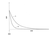
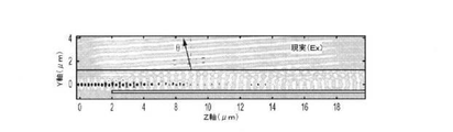
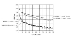
図1−1は、寿命の異なる2つのマーカの、時間に関する光子放出の確率をグラフにしたものである。確率曲線Bにより表されるマーカの放出確率は、確率曲線Aにより表されるマーカの放出確率より速く減衰する。確率曲線Bにより表されるマーカは、確率曲線Aにより表されるマーカより短い時間的パラメータτ、すなわち寿命を有する。マーカの寿
命は、いくつかの実施形態において、0.1〜20nsの範囲であってもよい。しかしながら、本明細書に記載されている技術は、使用されるマーカの寿命に関して限定されない。
FIG. 1-1 is a graph showing the probabilities of photon emission with respect to time of two markers having different lifetimes. The emission probability of the marker represented by the probability curve B decays faster than the emission probability of the marker represented by the probability curve A. The marker represented by the probability curve B has a shorter temporal parameter τ, that is, a lifetime, than the marker represented by the probability curve A. The lifetime of the marker may be in the range of 0.1 to 20 ns in some embodiments. However, the techniques described herein are not limited with respect to the lifetime of the markers used.
マーカの寿命は、複数のマーカ間で区別するために使用されてもよく、および/またはマーカの識別のために使用されてもよい。いくつかの実施形態において、異なる寿命の複数のマーカが励起源により励起される寿命測定が行われてもよい。一例として、寿命がそれぞれ0.5、1、2、および3ナノ秒の4つのマーカは、選択された波長(例えば、635nm等)を有する光を放出する光源により励起されてもよい。マーカは、マーカにより放出される光の寿命を測定することに基づいて識別されるか、または相互に区別されてもよい。 Marker life may be used to distinguish between multiple markers and / or to identify markers. In some embodiments, lifetime measurements may be made in which multiple markers with different lifetimes are excited by the excitation source. As an example, the four markers with lifetimes of 0.5, 1, 2, and 3 nanoseconds, respectively, may be excited by a light source that emits light having a selected wavelength (eg, 635 nm, etc.). Markers may be identified or distinguished from each other based on measuring the lifetime of light emitted by the markers.
寿命測定は、絶対的な強度の数値と対照的に、時間と共に強度がどのように変化するかを比較することによって相対的強度測定を使用してもよい。その結果、寿命測定は、絶対的強度測定の困難の一部を回避できる。絶対的強度測定は、存在するマーカの濃度に依存していてもよく、マーカの濃度を変化させるための校正ステップが必要であり得る。これに対して、寿命測定は、マーカの濃度により影響を受けないことがあり得る。 Lifespan measurements may use relative intensity measurements by comparing how the intensity changes over time, as opposed to absolute intensity numbers. As a result, life measurement can avoid some of the difficulties of absolute strength measurement. Absolute intensity measurements may depend on the concentration of markers present and may require calibration steps to change the concentration of markers. In contrast, lifespan measurements may be unaffected by marker concentrations.
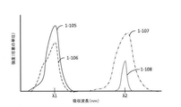
実施形態は、あるマーカの集合内の第一のマーカを同じ集合内の他のマーカから区別するために、マーカ特徴の何れの適当な組合せを使用してもよい。例えば、いくつかの実施形態は、マーカを識別するために、マーカからの放出光の時間情報のみを使用してもよい。このような実施形態において、選択されたマーカの集合内の各マーカは、その集合内の他のマーカと異なる放出寿命を有し、発光マーカの全てが単独の励起源からの光により励起される。図1−2Aは、ある実施形態による4つの発光マーカからの放出タイミングを示しており、4つのマーカは異なる放出寿命(τ)を示す。あるマーカが測定され、特定の数値の寿命を有する確率は、本明細書において、そのマーカの「放出タイミング」と呼ばれる。第一の発光マーカからの第一の放出タイミング1−101は、τ1において寿命を有するピーク確率を有し、第二の発光マーカからの第二の放出対タイミング1−102は、τ2において寿命を有するピーク確率を有し、第三の発光マーカからの第三の放出タイミング1−103は、τ3において寿命を有するピーク確率を有し、第四の発光マーカからの第四の放出タイミング1−104は、τ4において寿命を有するピーク確率を有する。この実施形態において、4つの発光マーカの寿命確率ピークは、関係τ1<τ2<τ3<τ4の関係を満たす何れの適当な数値であってもよい。4つの放出タイミンググラフは、図1−2Aに示されるように、特定の発光マーカの寿命のわずかなばらつきにより、重複する場合としない場合がある。この実施形態において、4つのマーカによる励起源からの光の吸収が最大になる励起波長は実質的に等しいが、そうである必要はない。上述のマーカ集合を使用して、4つの異なる分子がこのマーカ集合からのそれぞれのマーカで標識されてもよく、マーカは単独の励起源を使用して励起されてもよく、マーカは、光学システムとセンサとを使用してマーカの放出寿命を検出することにより、相互に区別できる。図1−2Aは4つの異なるマーカを示しているが、何れの適当な数のマーカを使用してもよいと理解すべきである。 In embodiments, any suitable combination of marker features may be used to distinguish the first marker in a set of markers from other markers in the same set. For example, in some embodiments, only the time information of the emitted light from the marker may be used to identify the marker. In such an embodiment, each marker in the set of selected markers has a different emission lifetime than the other markers in the set, and all of the emission markers are excited by light from a single excitation source. .. FIG. 1-2A shows the emission timings from the four emission markers according to an embodiment, and the four markers show different emission lifetimes (τ). The probability that a marker will be measured and have a certain numerical lifetime is referred to herein as the "release timing" of that marker. The first emission timing 1-101 from the first emission marker has a peak probability of having a lifetime at τ1, and the second emission pair timing 1-102 from the second emission marker has a lifetime at τ2. The third emission timing 1-103 from the third emission marker has a peak probability to have a peak probability having a lifetime at τ3, and the fourth emission timing 1-104 from the fourth emission marker has. Has a peak probability of having a lifetime at τ4. In this embodiment, the lifetime probability peaks of the four light emitting markers may be any appropriate numerical value satisfying the relation τ1 <τ2 <τ3 <τ4. The four emission timing graphs may or may not overlap due to slight variations in the lifetime of a particular emission marker, as shown in FIG. 1-2A. In this embodiment, the excitation wavelengths that maximize the absorption of light from the excitation source by the four markers are substantially equal, but need not be. Using the marker set described above, four different molecules may be labeled with their respective markers from this marker set, the markers may be excited using a single excitation source, and the markers are optical systems. And the sensor can be used to detect the emission lifetime of the markers so that they can be distinguished from each other. Although FIG. 1-2A shows four different markers, it should be understood that any suitable number of markers may be used.
他の実施形態は、マーカの集合内のマーカの識別を判定するために、何れの適当なマーカ特徴の組合せを使用してもよい。使用可能なマーカ特徴の例としては、励起波長、放出波長、および放出寿命が含まれていてもよいが、これらに限定されない。マーカ特徴の組合せは位相空間を形成し、各マーカは、この位相空間内の点として表されてもよい。マーカの集合内のマーカは、集合内の各マーカ間の「距離」が、検出メカニズムが各マーカを集合内の他のマーカから区別できる程度に十分に大きくなるように選択されるべきである。例えば、いくつかの実施形態において、マーカのサブセットが同じ放出波長を有するが、異なる放出寿命および/または異なる励起波長を有するようなマーカの集合が選択され
てもよい。他の実施形態において、マーカのサブセットが同じ放出寿命を有するが、異なる放出波長および/または異なる励起波長を有するようなマーカの集合が選択されてもよい。他の実施形態において、マーカのサブセットが同じ励起波長を有するが、異なる放出波長および/または異なる放出寿命を有するようなマーカの集合が選択されてもよい。
In other embodiments, any combination of suitable marker features may be used to determine the identification of markers within a set of markers. Examples of usable marker features may include, but are not limited to, excitation wavelength, emission wavelength, and emission lifetime. The combination of marker features forms a topological space, and each marker may be represented as a point in this topological space. The markers in the set of markers should be selected so that the "distance" between each marker in the set is large enough that the detection mechanism can distinguish each marker from the other markers in the set. For example, in some embodiments, a set of markers may be selected such that a subset of markers have the same emission wavelength but different emission lifetimes and / or different excitation wavelengths. In other embodiments, a set of markers may be selected such that a subset of markers have the same emission lifetime, but different emission wavelengths and / or different excitation wavelengths. In other embodiments, a set of markers may be selected such that a subset of markers have the same excitation wavelength, but different emission wavelengths and / or different emission lifetimes.
例えば、限定ではないが、図1−2Bは、ある実施形態による4つの発光マーカからの放出スペクトルを示しており、マーカの2つが第一のピーク放出波長を有し、残りの2つのマーカが第二のピーク放出波長を有する。第一の発光マーカからの第一の放出スペクトル1−105は、λ1においてピーク放出波長を有し、第二の発光マーカからの第二の放出スペクトル1−106も、λ1においてピーク放出波長を有し、第三の発光マーカからの第三の発光スペクトル1−107はλ2においてピーク放出波長を有し、第四の発光マーカからの第四の放出スペクトル1−108も、λ2においてピーク放出波長を有する。この実施形態において、4つの発光マーカの放出ピークは、λ1<λ2を満たす何れの適当な数値であってもよい。ピーク放出波長が複数の発光マーカについて同じであるこのような実施形態において、同じ放出波長を有するマーカのスペクトル特徴は異なっていなければならない。例えば、λ1において放出する2つのマーカは、異なる放出寿命を有していてもよい。図1−3Aは、この状況を、放出波長および放出寿命により画定される位相空間で概略的に示している。第一のマーカは放出波長λ1と放出寿命τ1とを有し、第二のマーカは放出波長λ1と放出寿命τ4とを有し、第三のマーカは放出波長λ2と放出寿命τ1とを有し、第四のマーカは放出波長λ2と放出寿命τ4とを有する。このようにして、図1−3Aに示されるマーカの4つのマーカは全て、相互に区別可能である。このようなマーカ集合を使用することにより、4つのマーカに関する吸収波長が同じであったとしても、4つのマーカ間を区別できる。これは、放出波長の他に、フォトルミネッセンスの放出時間を検出できるセンサを使用して可能となる。 For example, without limitation, FIG. 1-2B shows emission spectra from four emission markers according to an embodiment, two of which have the first peak emission wavelength and the other two markers. It has a second peak emission wavelength. The first emission spectrum 1-105 from the first emission marker has a peak emission wavelength at λ1, and the second emission spectrum 1-106 from the second emission marker also has a peak emission wavelength at λ1. Then, the third emission spectrum 1-107 from the third emission marker has a peak emission wavelength at λ2, and the fourth emission spectrum 1-108 from the fourth emission marker also has a peak emission wavelength at λ2. Have. In this embodiment, the emission peaks of the four emission markers may be any appropriate numerical value satisfying λ1 <λ2. In such an embodiment where the peak emission wavelength is the same for multiple emission markers, the spectral characteristics of the markers having the same emission wavelength must be different. For example, the two markers that emit at λ1 may have different emission lifetimes. FIG. 1-3A schematically illustrates this situation in a phase space defined by emission wavelength and emission lifetime. The first marker has an emission wavelength λ1 and an emission lifetime τ1, the second marker has an emission wavelength λ1 and an emission lifetime τ4, and the third marker has an emission wavelength λ2 and an emission lifetime τ1. , The fourth marker has an emission wavelength λ2 and an emission lifetime τ4. In this way, all four markers of the markers shown in FIG. 1-3A are distinguishable from each other. By using such a marker set, it is possible to distinguish between the four markers even if the absorption wavelengths of the four markers are the same. This is possible using a sensor that can detect the emission time of photoluminescence in addition to the emission wavelength.
例えば、限定ではないが、図1−2Cは、他の実施形態による4つの発光マーカからの吸収スペクトルを示す。この実施形態において、マーカの2つは第一のピーク吸収波長を有し、他の2つのマーカは第二のピーク吸収波長を有する。第一の発光マーカに関する第一の吸収スペクトル1−109はλ3においてピーク吸収波長を有し、第二の発光マーカに関する第二の吸収スペクトル1−110はλ4においてピーク吸収波長を有し、第三の発光マーカに関する第三の吸収スペクトル1−111はλ3においてピーク吸収波長を有し、第四の発光マーカに関する第四の吸収スペクトル1−112はλ4においてピーク吸収波長を有する。図1−2Cにおいてピーク吸収波長を共有するマーカは、別のマーカ特徴、例えば放出寿命等により区別可能である点に留意されたい。図1−3Bは、この状況を、吸収波長および放出寿命により画定される位相空間内で概略的に示している。第一のマーカは吸収長λ3と放出寿命τ1とを有し、第二のマーカは吸収波長λ3と放出寿命τ4とを有し、第三のマーカは吸収波長λ4と放出寿命τと1を有し、第四のマーカは吸収波長λ4と放出寿命τ4とを有する。このようにして、図1−3Aに示されるマーカ集合の4つの全てのマーカは相互に区別可能である。 For example, but not limited to, FIG. 1-2C shows absorption spectra from four emission markers according to other embodiments. In this embodiment, two of the markers have a first peak absorption wavelength and the other two markers have a second peak absorption wavelength. The first absorption spectrum 1-109 for the first emission marker has a peak absorption wavelength at λ3, the second absorption spectrum 1-110 for the second emission marker has a peak absorption wavelength at λ4, and the third The third absorption spectrum 1-111 of the emission marker has a peak absorption wavelength at λ3, and the fourth absorption spectrum 1-112 of the fourth emission marker has a peak absorption wavelength at λ4. It should be noted that the markers sharing the peak absorption wavelength in FIG. 1-2C can be distinguished by another marker feature, such as emission lifetime. FIG. 1-3B schematically illustrates this situation in a phase space defined by absorption wavelength and emission lifetime. The first marker has an absorption length λ3 and an emission lifetime τ1, the second marker has an absorption wavelength λ3 and an emission lifetime τ4, and the third marker has an absorption wavelength λ4 and an emission lifetime τ and 1. However, the fourth marker has an absorption wavelength λ4 and an emission lifetime τ4. In this way, all four markers in the marker set shown in FIG. 1-3A are distinguishable from each other.
このようなマーカ集合を使用することによって、4つのマーカの放出波長が区別不能であったとしても、4つのマーカ間の区別が可能である。これは、異なる波長を放出する2つの励起源または複数の波長で放出可能な単独の励起源を、フォトルミネッセンスの放出時間を検出できるセンサと共に使用することにより可能である。励起光の波長が検出される放出イベントごとにわかっていれば、何れのマーカが存在するかを判断できる。励起源は、第一の励起波長と第二の励起波長とで交互に切り換えられてもよく、これはインタリーブと呼ばれる。あるいは、第一の励起波長の2つ以上のパルスを、第二の励起波長の2つ以上のパルスの後に使用してもよい。 By using such a marker set, even if the emission wavelengths of the four markers are indistinguishable, it is possible to distinguish between the four markers. This is possible by using two excitation sources that emit different wavelengths or a single excitation source that can emit at multiple wavelengths, in combination with a sensor that can detect the emission time of photoluminescence. If the wavelength of the excitation light is known for each emission event detected, it is possible to determine which marker is present. The excitation source may be switched alternately between the first excitation wavelength and the second excitation wavelength, which is called interleaving. Alternatively, two or more pulses of the first excitation wavelength may be used after the two or more pulses of the second excitation wavelength.
マーカを区別するために使用される励起源または励起波長の数は、2つに限定されず、
いくつかの実施形態において、マーカの識別に3つ以上の励起波長またはエネルギーが使用されてもよい。このような実施形態において、マーカは、複数の励起波長に応答して放出された光子の強度または数によって区別されてもよい。マーカは、マーカを特定の励起波長に曝すことに応答して放出された光子の数を検出することによって、複数のマーカから区別可能であってもよい。いくつかの実施形態において、マーカは、マーカを一度に複数の励起エネルギーのうちの1つで照明し、複数の励起エネルギーのうちでそのマーカが最も多い光子を放出した励起エネルギーを識別することによって区別されてもよい。他の実施形態において、マーカが異なる励起エネルギーに応答して放出した光子の数がマーカを識別するために使用されてもよい。第一の励起エネルギーに応じて光子を放出する確率が第二の励起エネルギーより高い第一のマーカは、第二の励起エネルギーに応答して光子を放出する確率が第一の励起エネルギーより高い第二のマーカから区別されてもよい。このようにして、異なる励起エネルギーに応答して特定の量の光子を放出する確率が区別可能であるマーカは、未知のマーカを異なる励起エネルギーに曝しながら、放出された光子を測定することによって識別されてもよい。このような実施形態において、マーカは、複数の励起エネルギーに曝されてもよく、マーカの識別は、そのマーカが何れかの光を放出したか否か、および/または放出された特定の数の光子を判定することによって実現されてもよい。何れの適当な数の励起エネルギー源が使用されてもよい。いくつかの実施形態において、異なるマーカ(例えば、4つの異なるマーカ)間の区別に4つの異なる励起エネルギーが使用されてもよい。いくつかの実施形態において、異なるマーカ間の区別に3つの異なる励起エネルギーが使用されてもよい。マーカの存在を区別するために、放出寿命および放出スペクトルを含め、異なる励起エネルギーに応答して放出された光子の量と共に、マーカのその他の特徴が使用されてもよい。
The number of excitation sources or excitation wavelengths used to distinguish the markers is not limited to two.
In some embodiments, three or more excitation wavelengths or energies may be used to identify the markers. In such embodiments, the markers may be distinguished by the intensity or number of photons emitted in response to multiple excitation wavelengths. The marker may be distinguishable from the plurality of markers by detecting the number of photons emitted in response to exposing the marker to a particular excitation wavelength. In some embodiments, the marker illuminates the marker with one of a plurality of excitation energies at a time and identifies the excitation energy of which the marker emits the most photons of the plurality of excitation energies. It may be distinguished. In other embodiments, the number of photons emitted by the marker in response to different excitation energies may be used to identify the marker. The first marker, which has a higher probability of emitting photons in response to the first excitation energy than the second excitation energy, has a higher probability of emitting photons in response to the second excitation energy than the first excitation energy. It may be distinguished from the second marker. In this way, markers whose probabilities of emitting a particular amount of photons in response to different excitation energies are distinguishable are identified by measuring the emitted photons while exposing the unknown marker to different excitation energies. May be done. In such an embodiment, the marker may be exposed to multiple excitation energies, and the identification of the marker is whether or not the marker emits any light and / or a specific number of emitted light. It may be realized by determining a photon. Any suitable number of excitation energy sources may be used. In some embodiments, four different excitation energies may be used to distinguish between different markers (eg, four different markers). In some embodiments, three different excitation energies may be used to distinguish between different markers. Other features of the marker may be used, along with the amount of photons emitted in response to different excitation energies, including emission lifetime and emission spectrum to distinguish the presence of the marker.
他の実施形態において、マーカ集合内のマーカの3つ以上の特徴がマーカの存在を区別するために使用されてもよい。図1−4は、マーカの吸収波長、放出波長、および放出寿命により画定される例示的な位相空間を示している。図1−4において、8つの異なるマーカが位相空間内で分散されている。8つのマーカのうちの4つは、同じ放出波長を有し、異なる4つのマーカは同じ吸収波長を有し、異なる4つのマーカは同じ放出寿命を有する。しかしながら、マーカの各々は、マーカの3つ全ての特徴が考慮されたときに、他の個々のマーカから区別可能である。実施形態は、マーカの何れの数にも限定されない。この概念は、少なくともこれら3つのマーカ特徴を使用して、相互に区別可能な何れの数のマーカを含むことにも拡張できる。 In other embodiments, three or more features of the markers in the marker set may be used to distinguish the presence of the markers. FIG. 1-4 shows an exemplary topological space defined by the absorption wavelength, emission wavelength, and emission lifetime of the marker. In FIG. 1-4, eight different markers are dispersed in the topological space. Four of the eight markers have the same emission wavelength, four different markers have the same absorption wavelength, and four different markers have the same emission lifetime. However, each of the markers is distinguishable from the other individual markers when all three features of the marker are taken into account. The embodiment is not limited to any number of markers. This concept can be extended to include any number of mutually distinguishable markers using at least these three marker features.
図中には示されていないが、他の実施形態は、吸収周波数のみに基づいて発光マーカの識別を判定してもよい。このような実施形態は、励起光が、マーカ集合内のマーカの吸収スペクトルとマッチする特定の波長に調整できれば可能である。このような実施形態において、各マーカにより放出される光を誘導し、検出するために使用される光学システムセンサは、放出光の波長を検出できなくてもよい。これは、いくつかの実施形態において、そのような実施形態では放出波長の検出が不要であることから、光学システムとセンサとが単純化するため、有利であり得る。 Although not shown in the figure, other embodiments may determine the identification of the emission marker based solely on the absorption frequency. Such an embodiment is possible if the excitation light can be adjusted to a specific wavelength that matches the absorption spectrum of the markers in the marker set. In such an embodiment, the optical system sensor used to guide and detect the light emitted by each marker may not be able to detect the wavelength of the emitted light. This can be advantageous in some embodiments because it simplifies the optical system and the sensor because it does not require detection of the emission wavelength.
上述のように、本発明者らは、異なる発光マーカを、マーカの様々な特徴を使用して相互に区別できる必要性を認識し、理解した。マーカの識別を判定するために使用される特徴の種類は、この解析を実行するために使用される物理的装置に影響を与える。本願は、このような異なる実験を実行するための装置、デバイス、機器、および方法のいくつかの実施形態を開示する。 As mentioned above, we have recognized and understood the need for different emission markers to be distinguished from each other using the various characteristics of the markers. The type of feature used to determine the identification of the marker affects the physical equipment used to perform this analysis. The present application discloses several embodiments of devices, devices, devices, and methods for performing such different experiments.
本発明者らは、光学系およびセンサを含む低コストの単回使用使い捨て集積装置を、励起源を含む機器と共に使用して、生物検体を標識するために使用された1つまたはマーカから放出された発光の異なる特徴を測定することによって検体を解析してもよいことを認
識し、そのように理解した。低コストの集積装置の使用により、所定のバイオアッセイで実行コストが削減される。生物検体が集積装置上にセットされ、バイオアッセイが終了したら廃棄されてもよい。集積装置は、様々な使い捨ての集積装置と共に繰返し使用されてもよい、より高価で複数回使用される機器とインタフェースする。小型のポータブル機器とインタフェースする低コストの集積装置は、世界の何れの場所でも使用でき、検体解析のために研究の専門知識を必要とする高コストの生物学的研究所の制約を受けない。そのため、世界においてこれまで生物検体の定量解析を行うことのできなかった地域に自動生体解析がもたらされ得る。例えば、乳児の血液検査は、血液検体を使い捨て集積装置の上に載せ、使い捨て集積装置を小型のポータブルの解析機器にセットし、結果を機器に接続されたコンピュータで処理して、使用者が即時にそれを見られるようにすることによって実行してもよい。データはまた、データネットワーク上で離れた場所に転送することにより、解析され、および/または後に臨床解析するために保存されてもよい。あるいは、機器はまた、集積装置のセンサから得たデータを解析するための1つまたは複数のプロセッサを含んでいてもよい。
We use a low-cost, single-use, single-use integration device that includes optics and sensors with equipment that includes an excitation source to be released from one or marker used to label a biological specimen. We recognized and understood that the specimens could be analyzed by measuring the different characteristics of the luminescence. The use of low-cost integration equipment reduces the cost of execution in a given bioassay. The biological specimen may be set on the accumulator and discarded after the bioassay is complete. The integration device interfaces with more expensive and multiple-use equipment that may be used repeatedly with various disposable integration devices. Low-cost integration devices that interface with small portable devices can be used anywhere in the world and are not constrained by high-cost biological laboratories that require research expertise for sample analysis. Therefore, automatic bioanalysis can be brought to areas in the world where quantitative analysis of biological specimens has not been possible so far. For example, in an infant's blood test, a blood sample is placed on a disposable accumulator, the disposable accumulator is set in a small portable analysis device, and the result is processed by a computer connected to the device, and the user can immediately perform it. It may be done by making it visible to the computer. The data may also be analyzed and / or stored for later clinical analysis by transferring it to a remote location on the data network. Alternatively, the instrument may also include one or more processors for analyzing the data obtained from the sensors of the integrated device.
各種の実施形態を以下により詳しく説明する。
I.システムの概要
システムは、集積装置と、集積装置とインタフェースするように構成された機器とを含む。集積装置はピクセルのアレイを含み、ピクセルは検体ウェルと、少なくとも1つのセンサとを含む。集積装置の表面には複数の検体ウェルがあり、検体ウェルは、集積装置の表面上に載せられた試料からの検体を受けるように構成される。試料は複数の検体、いくつかの実施形態において、異なる種類の検体を含んでいてもよい。複数の検体ウェルは、検体ウェルの少なくとも一部が試料からの1つの検体を受けるように構成される設計であってもよい。いくつかの実施形態において、検体ウェル内の検体の数は検体ウェル間で分散されてもよく、1つの検体を収容する検体ウェルがあれば、検体が収容されない、または2つ以上の検体を収容する検体ウェルもある。例えば、試料には複数の一本鎖DNA鋳型が含まれていてもよく、集積装置の表面上の検体ウェルは、1つの一本鎖DNA鋳型を受けてもよい。集積装置の検体ウェルの少なくとも一部は、一本鎖DNA鋳型を収容してもよい。試料にはまた、タグ付きdNTPが含まれていてもよく、これはその後、検体ウェルに入り、それがDNAの相補的な鎖内に組み込まれるときにヌクレオチドの識別が可能になり得る。このような例において、「検体」とは、一本鎖DNAとポリメラーゼによって現在組み込まれているタグ付きdNTPとの両方を指してもよい。いくつかの実施形態において、試料には一本鎖DNA鋳型が含まれていてもよく、タグ付きdNTPはその後、検体ウェル内に、ヌクレオチドがその検体ウェル内のDNA相補的な鎖内に組み込まれたときに導入され得る。このようにして、ヌクレオチド組込みのタイミングは、タグ付きdNTPが集積装置の検体ウェル内にいつ導入されるかによって制御されてもよい。
Various embodiments will be described in more detail below.
I. System Overview The system includes an integrated device and equipment configured to interface with the integrated device. The integration device includes an array of pixels, the pixels including a sample well and at least one sensor. There are a plurality of sample wells on the surface of the accumulator, and the sample wells are configured to receive a sample from a sample placed on the surface of the accumulator. The sample may include a plurality of samples, different types of samples in some embodiments. The plurality of sample wells may be designed so that at least a part of the sample wells receives one sample from the sample. In some embodiments, the number of specimens in a specimen well may be dispersed among the specimen wells, with a specimen well accommodating one specimen, no specimen accommodating, or accommodating two or more specimens. There is also a sample well to do. For example, the sample may contain a plurality of single-stranded DNA templates, and the sample wells on the surface of the accumulator may receive one single-stranded DNA template. At least a portion of the sample well of the accumulator may contain a single-stranded DNA template. The sample may also contain a tagged dNTP, which can then enter the sample well and allow nucleotide identification when it is incorporated into the complementary strand of DNA. In such an example, "specimen" may refer to both the single-stranded DNA and the tagged dNTP currently incorporated by the polymerase. In some embodiments, the sample may include a single-stranded DNA template, where the tagged dNTP is then incorporated into the sample well and the nucleotides are incorporated into the DNA complementary strand within the sample well. Can be introduced at the time. In this way, the timing of nucleotide integration may be controlled by when the tagged dNTPs are introduced into the sample wells of the accumulator.
励起エネルギーは、集積装置のピクセルアレイから離れた場所にある励起源から提供される。励起エネルギーは、少なくとも部分的に、集積装置の要素によって1つまたは複数のピクセルに向かって誘導され、検体ウェル内の照明領域を照明する。したがって、マーカまたはタグは、照明領域内にあるときに、励起エネルギーにより照明されたことに応答して放出エネルギーを放出してもよい。いくつかの実施形態において、1つまたは複数の励起源はシステムの機器の一部であり、機器の構成要素および集積装置は、励起エネルギーを1つまたは複数のピクセルに向かって誘導するように構成される。他の実施形態において、1つまたは複数の励起源は、集積装置上であるがピクセルのアレイとは別の領域に位置付けられ、集積装置内の構成要素は、励起源領域からの励起エネルギーを1つまたは複数のピクセルに誘導するように構成される。 The excitation energy is provided by an excitation source located away from the pixel array of the integrated device. The excitation energy is, at least in part, guided towards one or more pixels by the elements of the integration device to illuminate the illuminated area within the specimen well. Thus, the marker or tag may emit emission energy in response to being illuminated by excitation energy when in the illuminated area. In some embodiments, the one or more sources of excitation are part of the equipment of the system, and the components and integration of the equipment are configured to direct the excitation energy towards one or more pixels. Will be done. In other embodiments, the one or more excitation sources are located on the integration device but in a region separate from the pixel array, and the components within the integration device are one of the excitation energies from the excitation source region. It is configured to guide to one or more pixels.
次に、検体により放出された放出エネルギーは集積装置のピクセル内の1つまたは複数のセンサにより検出されてもよい。いくつかの実施形態において、複数のセンサは放出エ
ネルギーの空間的分散を捕捉する大きさおよび配置であってもよい。いくつかの実施形態において、1つまたは複数のセンサは、検体の放出エネルギーに関連付けられるタイミングの特徴(例えば、蛍光寿命)を検出するように構成されてもよい。したがって、1つまたは複数のセンサからの出力信号は、複数のマーカからマーカを区別するために使用されてもよく、この複数のマーカは、試料内のある検体を識別するために使用されてもよい。いくつかの実施形態において、検体は、複数の励起エネルギーによって励起されてもよく、複数の励起エネルギーに応答して検体により放出された放出エネルギーおよび/または放出エネルギーのタイミングの特徴は、複数のマーカからあるマーカを区別できる。
The released energy released by the specimen may then be detected by one or more sensors within the pixels of the accumulator. In some embodiments, the sensors may be of a size and arrangement that captures the spatial dispersion of emitted energy. In some embodiments, the sensor may be configured to detect timing characteristics (eg, fluorescence lifetime) associated with the emission energy of the specimen. Therefore, the output signal from one or more sensors may be used to distinguish a marker from a plurality of markers, and the plurality of markers may be used to identify a sample in a sample. good. In some embodiments, the specimen may be excited by multiple excitation energies, and the emission energy and / or timing characteristics of the emission energy emitted by the specimen in response to the plurality of excitation energies are characterized by multiple markers. Can distinguish certain markers from.
システム2−100の概略が図2−1Aおよび2−1Bに示されている。システムは、機器2−104とインタフェースする集積装置2−102の両方を含む。いくつかの実施形態において、機器2−104は1つまたは複数の励起源2−106を含んでいてもよい。いくつかの実施形態において、励起源は機器2−104と集積装置2−102との両方の外にあってもよく、機器2−104は励起エネルギーを励起源から受け取り、それを集積装置に誘導するように構成されていてもよい。集積装置は、集積装置を受け、それを励起源と正確に光学的に整列した状態に保持するためのあらゆる適当なソケットを使用して機器とインタフェースする。励起源2−106は、励起エネルギーを集積装置2−102に提供するように構成されてもよい。励起源は図2−1Bにおいて機器内にあるように示されているが、励起源は、いくつかの例において、集積装置上の、ピクセルから離れた領域に位置付けられてもよい。図2−1Bに概略的に示されているように、集積装置2−102は複数のピクセルを有し、各ピクセル2−112は検体の独立した解析が可能である。このようなピクセル2−112は「パッシブソースピクセル」と呼ばれてもよく、それは、ピクセルがそのピクセルから離れた励起源2−106から励起エネルギーを受け取り、励起源が複数のピクセルを励起させるからである。各ピクセル2−112は、検体を保持し、解析するための検体ウェル2−108と、励起源2−106により提供される励起エネルギーで検体が照明されたことに応答して検体により放出された放出エネルギーを検出するためのセンサ2−110とを有する。いくつかの実施形態において、各センサ2−110は複数のサブセンサを含んでいてもよく、各サブセンサは、検体からの放出エネルギーの異なる波長を検出するように構成される。 A schematic of System 2-100 is shown in Figures 2-1A and 2-1B. The system includes both integrated devices 2-102 that interface with equipment 2-104. In some embodiments, instrument 2-104 may include one or more excitation sources 2-106. In some embodiments, the excitation source may be outside of both instrument 2-104 and integration device 2-102, where instrument 2-104 receives excitation energy from the excitation source and directs it to the integration device. It may be configured to do so. The agglomerator receives the agglomerator and interfaces with the instrument using any suitable socket to keep it precisely optically aligned with the excitation source. The excitation source 2-106 may be configured to provide excitation energy to the integration device 2-102. Although the excitation source is shown in FIG. 2-1B to be in the instrument, the excitation source may, in some examples, be located in a region away from the pixels on the integration device. As schematically shown in FIG. 2-1B, the integration device 2-102 has a plurality of pixels, each pixel 2-112 capable of independent analysis of the specimen. Such pixels 2-112 may also be referred to as "passive source pixels" because the pixels receive excitation energy from excitation sources 2-106 away from the pixels and the excitation sources excite multiple pixels. Is. Each pixel 2-112 was released by the sample in response to illumination of the sample with the sample well 2-108 for holding and analyzing the sample and the excitation energy provided by the excitation source 2-106. It has sensors 2-110 for detecting emitted energy. In some embodiments, each sensor 2-110 may include a plurality of subsensors, each subsensor being configured to detect different wavelengths of energy emitted from the specimen.
励起エネルギーを検体ウェル2−108に案内し、結合するための光学要素は、集積装置2−102と機器2−104との両方にある。このようなソース−ウェル要素は、集積装置2−102の上にあり、励起エネルギーを集積装置に結合するための回折格子カプラ、励起エネルギーを各ピクセル2−112に送達するための導波路、およびレンズ、プラズモン要素、ならびに集積装置上にあり、機器2−104から受け取られた励起エネルギーを検体ウェル2−108に誘導する誘電性コーティングを含んでいてもよい。それに加えて、集積装置上にある光学要素は、放出エネルギーを検体ウェルからセンサに向かって誘導する。このようなウェル−検体要素は、放出エネルギーを放射パターンに誘導する構成要素を含んでいてもよく、放射パターンは検体ウェル内で検体が放出する放出エネルギーに依存する。検体ウェル2−108、ソース−ウェル光学系の一部、および検体ウェル−センサ光学系は、集積装置2−102の上にある。励起源2−106およびソース−ウェル構成要素の一部は、機器2−104内にある。いくつかの実施形態において、1つの構成要素が、励起エネルギーを検体ウェル2−108に結合することと、放出エネルギーを検体ウェル2−108からセンサ2−110へと送達することとの両方において役割を果たしてもよい。 Optical elements for directing and coupling excitation energy to specimen wells 2-108 are located in both the integration device 2-102 and the device 2-104. Such a source-well element resides on the integration device 2-102, a grating coupler for coupling the excitation energy to the integration device, a waveguide for delivering the excitation energy to each pixel 2-112, and a waveguide. It may include a lens, a plasmon element, and a dielectric coating that is on the integrating device and directs the excitation energy received from the device 2-104 to the sample well 2-108. In addition, the optics on the integration device direct the emitted energy from the specimen well towards the sensor. Such a well-specimen element may include components that direct the emission energy into a radiation pattern, which depends on the emission energy emitted by the sample within the sample well. The specimen well 2-108, part of the source-well optics, and the specimen well-sensor optics are on the integration device 2-102. Excitation source 2-106 and some of the source-well components are within instrument 2-104. In some embodiments, one component plays a role in both binding excitation energy to sample well 2-108 and delivering released energy from sample well 2-108 to sensor 2-110. May be fulfilled.
図2−1Bに示されているように、集積装置は複数のピクセルを含み、各ピクセル2−112がそれ自体の個々の検体ウェル2−108およびセンサ2−110に関連付けられる。複数のピクセルは、アレイ状に配置されてもよく、何れの適当な数のピクセルがあってもよい。例えば、集積装置2−102は、いくつかの実施形態によれば100〜1,0
00ピクセル、いくつかの実施形態によれば1,000〜10,000ピクセル、いくつかの実施形態によれば10,000〜100,000ピクセル、いくつかの実施形態によれば100,000〜1,000,000ピクセル、さらにいくつかの実施形態によれば1,000,000〜10,000,000ピクセルを含んでいてもよい。いくつかの実施形態において、集積装置2−102には、それより少ないまたはそれより多いピクセルがあってもよい。集積装置2−102と機器2−104とは、大きいピクセルアレイ(例えば、1000を超えるピクセル)に関連付けられるデータを取り扱うための多チャンネル高速通信リンクを含んでいてもよい。
As shown in FIG. 2-1B, the integration device comprises a plurality of pixels, each pixel 2-112 being associated with its own individual sample well 2-108 and sensor 2-110. The plurality of pixels may be arranged in an array, and there may be any appropriate number of pixels. For example, the integration device 2-102 is 100 to 1,0 according to some embodiments.
00 pixels, 1,000 to 10,000 pixels according to some embodiments, 10,000 to 100,000 pixels according to some embodiments, 100,000 to 1 according to some embodiments It may include, million pixels, and according to some embodiments, 1,000,000 to 1,000,000 pixels. In some embodiments, the integration device 2-102 may have fewer or more pixels. The integration device 2-102 and the device 2-104 may include a multi-channel high-speed communication link for handling data associated with a large pixel array (eg, more than 1000 pixels).
励起源2−106は、励起エネルギーを少なくとも1つの検体ウェルに送達するように配置された何れの適当な励起源であってもよい。いくつかの実施形態において、1つまたは複数の励起源のアレイが、同じ集積装置上のピクセルアレイに隣接して配置される。他の実施形態において、1つまたは複数の励起源は、ピクセルアレイが形成されている基板に近接して取り付けられた第二の基板の上にある。 Excitation source 2-106 may be any suitable excitation source arranged to deliver excitation energy to at least one sample well. In some embodiments, an array of one or more sources of excitation is placed adjacent to a pixel array on the same integration device. In other embodiments, the one or more sources of excitation are on a second substrate mounted in close proximity to the substrate on which the pixel array is formed.
機器2−104は、集積装置インタフェース2−114を通じて集積装置2−102とインタフェースする。集積装置インタフェース2−114は、集積装置2−102を機器2−104に位置付け、および/または整列させて、励起源2−106からの励起エネルギーの集積装置2−102への結合を改善する構成要素を含んでいてもよい。いくつかの実施形態において、励起源2−106は、複数の励起源を含み、これらは組み合わせて励起エネルギーを集積装置2−102に送達する。複数の励起源は、複数の励起エネルギーまたは波長を生成するように構成されてもよい。集積装置インタフェース2−114は、集積装置上にあるピクセル内のセンサからの読取り信号を受け取ってもよい。それに加えて、集積装置インタフェース2−114は、集積装置を集積装置インタフェース2−114に固定することにより、集積装置が機器に取り付けられるように設計されてもよい。 Equipment 2-104 interfaces with the integration device 2-102 through the integration device interface 2-114. The integration device interface 2-114 positions and / or aligns the integration device 2-102 with the instrument 2-104 to improve the coupling of excitation energy from the excitation source 2-106 to the integration device 2-102. It may contain elements. In some embodiments, the excitation sources 2-106 include a plurality of excitation sources, which in combination deliver excitation energy to the integration device 2-102. The plurality of excitation sources may be configured to generate multiple excitation energies or wavelengths. The integration device interface 2-114 may receive a read signal from a sensor within a pixel on the integration device. In addition, the integrated device interface 2-114 may be designed so that the integrated device can be attached to the device by fixing the integrated device to the integrated device interface 2-114.
機器2−104は、機器2−104の動作を制御するユーザインタフェース2−116を含む。ユーザインタフェース2−116は、使用者が、機器の機能を制御するために使用されるコマンドおよび/または設定等の情報を機器に入力できるように構成される。いくつかの実施形態において、ユーザインタフェース2−116は、ボタン、スイッチ、ダイアル、および音声コマンドのためのマイクロフォンを含んでいてもよい。それに加えてユーザインタフェース2−116により、使用者は機器および/または集積装置の性能についてのフィードバック、例えば集積装置上のセンサからの読取り信号により得られた適正なアラインメントおよび/または情報を受け取ることができ得る。いくつかの実施形態において、ユーザインタフェース2−116は、可聴的フィードバックを提供するためのスピーカおよび視覚的フィードバックを提供するためのインジケータランプおよび/またはディスプレイスクリーンを使用してフィードバックを提供してもよい。いくつかの実施形態において、機器2−104は、コンピューティングデバイス2−120と接続するために使用されるコンピュータインタフェース2−118を含む。何れの適当なコンピュータインタフェース2−118とコンピューティングデバイス2−120とが使用されてもよい。例えば、コンピュータインタフェース2−118は、USBインタフェースまたはファイヤワイヤインタフェースであってもよい。コンピューティングデバイス2−120は、ラップトップまたはデスクトップコンピュータ等の何れの汎用コンピュータであってもよい。コンピュータインタフェース2−118は、機器2−104とコンピューティングデバイス2−120との間での情報を通信しやすくする。機器2−104を制御および/または構成するための入力情報は、機器のコンピュータインタフェース2−118に接続されたコンピューティングデバイス2−120を通じて提供されてもよい。それに加えて、出力情報はコンピュータインタフェース2−118を通じてコンピューティングデバイス2−120によって受け取られてもよい。このような出力情報には、機器2−104および/またはまたは集積装置2−112の性能に関するフィードバックおよびセンサ2
−110の読取り信号からの情報が含まれていてもよい。機器2−104はまた、センサ2−110から受け取られたデータを解析し、および/または制御信号を励起源2−106に送信するための処理装置2−122も含んでいてよい。いくつかの実施形態において、処理装置2−122は、汎用プロセッサ、専用に調整されたプロセッサ(例えば、1つまたは複数のマイクロプロセッサまたはマイクロコントローラコア、フィールドプログラマブルゲートアレイ(FPGA:field−programmable integrated circuit)、特定用途集積回路(ASIC:application−specific integrated circuit)、カスタム集積回路、デジタル信号プロセッと(DSP:digital signal processor)、またはそれらの組合せなどの中央処理装置(CPU:central processing unit))を含んでいてもよい。いくつかの実施形態において、センサ2−110からのデータの処理は、処理装置2−122と外部コンピューティングデバイス2−120との両方で行われてもよい。他の実施形態において、コンピューティングデバイス2−120を省略してもよく、センサ2−110からのデータの処理は処理装置2−122によってのみ行われてもよい。
Device 2-104 includes a user interface 2-116 that controls the operation of device 2-104. User interface 2-116 is configured to allow the user to enter information such as commands and / or settings used to control the functionality of the device into the device. In some embodiments, user interface 2-116 may include microphones for buttons, switches, dials, and voice commands. In addition, the user interface 2-116 allows the user to receive feedback on the performance of the equipment and / or the integrated device, eg, proper alignment and / or information obtained by reading signals from sensors on the integrated device. Can be done. In some embodiments, user interface 2-116 may provide feedback using speakers to provide audible feedback and indicator lamps and / or display screens to provide visual feedback. .. In some embodiments, device 2-104 comprises computer interface 2-118 used to connect to computing device 2-120. Any suitable computer interface 2-118 and computing device 2-120 may be used. For example, computer interface 2-118 may be a USB interface or a Firewire interface. The computing device 2-120 may be any general purpose computer such as a laptop or desktop computer. Computer interface 2-118 facilitates communication of information between device 2-104 and computing device 2-120. Input information for controlling and / or configuring device 2-104 may be provided through computing device 2-120 connected to computer interface 2-118 of the device. In addition, the output information may be received by the computing device 2-120 through computer interface 2-118. Such output information includes feedback on the performance of equipment 2-104 and / or integration device 2-112 and
It may contain information from the -110 read signal. Instrument 2-104 may also include processing apparatus 2-122 for analyzing data received from sensor 2-110 and / or transmitting control signals to excitation source 2-106. In some embodiments, the processor 2-122 is a general purpose processor, a specially tuned processor (eg, one or more microprocessors or microprocessor cores, field programmable gate arrays (FPGAs), field-programmable integrated circuits). ), Special application integrated circuit (ASIC), custom integrated circuit, digital signal processor (DSP), or a central processing unit (CPU) such as a combination thereof. It may be included. In some embodiments, processing of data from sensor 2-110 may be performed by both processing device 2-122 and external computing device 2-120. In other embodiments, the computing device 2-120 may be omitted and the processing of data from the sensor 2-110 may be performed only by the processing device 2-122.
ピクセルの行を例示する集積装置3−102の断面図が図3−1Aに示されている。各ピクセル3−112は、検体ウェル3−108とセンサ3−110とを含む。センサ3−110は、検体ウェル3−112と整列され、位置付けられていてもよい。励起源が集積装置に結合されているとき、励起エネルギーは1つまたは複数のピクセルに提供される。図3−1Bは、励起源3−106を集積装置3−102に結合することを示す概略図である。励起源3−106は、集積装置3−102内で励起エネルギー3−130(破線で示される)を提供する。図3−1Bは、励起エネルギー源3−106からピクセル3−112内の検体ウェル3−108への励起エネルギーの経路を示している。集積装置の外にある構成要素は、励起源3−106を集積装置に位置付けて、整列させるために使用されてもよい。このような構成要素は、レンズ、ミラー、プリズム、絞り、減衰器および/または光ファイバを含む光学構成要素を含んでいてもよい。機器内には、1つまたは複数のアラインメント構成要素を制御できるように構成されたその他の機械的構成要素が含まれていてもよい。このような機械的構成要素には、アクチュエータ、ステップモータ、および/またはノブが含まれていてもよい。集積装置は、励起エネルギー3−130を集積装置内のピクセルに向かって誘導する構成要素を含む。各ピクセル3−112内で、励起エネルギーは、ピクセルに関連付けられる検体ウェル3−108に結合される。図3−1Bはピクセルの行内の各検体ウェルへの励起エネルギーの結合を示しているが、いくつかの実施形態において、励起エネルギーは、行内のピクセルの全てに結合しなくてもよい。いくつかの実施形態において、励起エネルギーは、集積装置のピクセルの行内のピクセルまたは検体ウェルの一部に結合されてもよい。励起エネルギーは、検体ウェル内にある検体を照明してもよい。検体は、励起エネルギーにより照明されたことに応答して励起状態に到達してもよい。検体が励起状態にあるとき、検体は放出エネルギーを放出してもよく、放出エネルギーはセンサにより検出されてもよい。図3−1Bは、検体ウェル3−108からピクセル3−112のセンサ3−110への放出エネルギー3−140(実線で示される)の経路を概略的に示している。ピクセル3−112内のセンサ3−110は、検体ウェル3−108からの放出エネルギーを検出するように構成され、位置付けられてもよい。いくつかの実施形態において、センサ3−110は1つまたは複数のサブセンサを含んでいてもよい。 A cross-sectional view of the integration device 3-102 exemplifying a row of pixels is shown in FIG. 3-1A. Each pixel 3-112 includes a specimen well 3-108 and a sensor 3-110. Sensor 3-110 may be aligned and positioned with specimen well 3-112. When the excitation source is coupled to the integration device, the excitation energy is provided to one or more pixels. FIG. 3-1B is a schematic diagram showing that the excitation source 3-106 is coupled to the integration device 3-102. Excitation source 3-106 provides excitation energy 3-130 (indicated by the dashed line) within the integration device 3-102. FIG. 3-1B shows the path of excitation energy from the excitation energy source 3-106 to the sample well 3-108 within pixel 3-112. Components outside the integration device may be used to position and align excitation sources 3-106 with the integration device. Such components may include optical components including lenses, mirrors, prisms, diaphragms, attenuators and / or optical fibers. The device may include other mechanical components configured to control one or more alignment components. Such mechanical components may include actuators, step motors, and / or knobs. The integration device includes components that direct the excitation energy 3-130 towards the pixels in the integration device. Within each pixel 3-112, the excitation energy is coupled to the sample well 3-108 associated with the pixel. Although FIG. 3-1B shows the binding of excitation energy to each sample well in a row of pixels, in some embodiments the excitation energy does not have to be bound to all of the pixels in the row. In some embodiments, the excitation energy may be coupled to a pixel or part of a sample well within a row of pixels in the accumulator. The excitation energy may illuminate the sample in the sample well. The specimen may reach an excited state in response to being illuminated by excitation energy. When the specimen is in an excited state, the specimen may release released energy, which may be detected by a sensor. FIG. 3-1B schematically shows the path of energy released 3-140 (shown by the solid line) from sample well 3-108 to sensor 3-110 of pixel 3-112. Sensor 3-110 within pixels 3-112 may be configured and positioned to detect the energy released from specimen well 3-108. In some embodiments, sensor 3-110 may include one or more subsensors.
解析対象の検体は、ピクセル3−112の検体ウェル3−108に導入されてもよい。検体は、生物検体または化学的検体などの他の何れの適当な検体であってもよい。検体は複数の分子を含んでいてよく、検体ウェルは単一分子を分離するように構成されてもよい。いくつかの例において、検体ウェルの寸法は、検体ウェル内に単一分子を閉じ込める役割を果たしてよく、単一分子上で測定を実行することを可能にする。励起源3−106は
、励起エネルギーを検体ウェル3−108に送達して、検体、または検体に付着されているか、またはその他の方法で検体に関連付けられている少なくとも1つの発光マーカを、それが検体ウェル3−108内の励起領域にある間に励起させるように構成されていてもよい。複数分子の検体において、1種類の発光マーカが分子の種類に一意的に関連付けられてもよい。励起中または励起後に、発光マーカは放出エネルギーを放出してもよい。複数のマーカが使用される場合、これらは異なる特徴的エネルギーを放出してもよい。いくつかの実施形態において、複数のマーカは異なる特徴的寿命を有していてもよい。それに加えて、多数のマーカは複数の励起エネルギーに対する応答において異なっていてもよい。検体のためのマーカは、その励起応答、特徴的エネルギーまたは波長、および/または特徴的寿命により識別されてもよい。検体からの放出は、検体ウェル3−108からセンサ3−110へと放射してもよい。
The sample to be analyzed may be introduced into sample well 3-108 of pixels 3-112. The sample may be any other suitable sample, such as a biological sample or a chemical sample. The sample may contain multiple molecules and the sample well may be configured to separate a single molecule. In some examples, the dimensions of the sample well may serve to confine a single molecule within the sample well, allowing measurements to be performed on a single molecule. Excitation source 3-106 delivers excitation energy to specimen well 3-108 to provide at least one luminescent marker that is attached to or otherwise associated with the specimen. It may be configured to be excited while in the excitation region within sample well 3-108. In a multi-molecule sample, one type of luminescence marker may be uniquely associated with the type of molecule. The emission marker may emit emission energy during or after excitation. If multiple markers are used, they may emit different characteristic energies. In some embodiments, the plurality of markers may have different characteristic lifetimes. In addition, many markers may differ in their response to multiple excitation energies. Markers for specimens may be identified by their excitation response, characteristic energy or wavelength, and / or characteristic lifetime. The release from the sample may be radiated from the sample well 3-108 to the sensor 3-110.
構成要素は、放出エネルギーをセンサに向かって集束させてもよく、それに加えてまたはその代わりに、特徴的エネルギーまたは波長を有する放出エネルギーを空間的に分離してもよい。励起源3−106から放出された励起エネルギーは、検体ウェル3−108に対して何れの適当な方法で誘導されてもよく、検体ウェル3−108内に受けられた少なくとも1つの検体を励起するように構成されてもよい。いくつかの実施形態によれば、励起源3−106は検体を励起させてもよく、これは発光し得る。励起源は、1つまたは複数の励起エネルギーを検体ウェル3−108に供給してもよい。いくつかの実施例において、励起源3−106は、1つまたは複数のマーカを励起させてもよく、これは励起に応答して発光し、またはエネルギーを放出し、検体に付着され、またはそれ以外の方法で検体に関連付けられる。励起の結果として放出された発光またはエネルギーは、センサ3−110へと誘導されてもよく、これは、受け取られた放出の強度および/またはタイミングを検出するように構成されてもよい。発光の非限定的な例は、フォトルミネッセンス、蛍光、燐光である。 The components may focus the emitted energy towards the sensor, and in addition or instead, may spatially separate the emitted energy with characteristic energy or wavelength. The excitation energy released from the excitation source 3-106 may be induced with respect to the sample well 3-108 by any suitable method, and excites at least one sample received in the sample well 3-108. It may be configured as follows. According to some embodiments, the excitation source 3-106 may excite the specimen, which may emit light. The excitation source may supply one or more excitation energies to sample wells 3-108. In some embodiments, the excitation source 3-106 may excite one or more markers, which emit light or emit energy in response to excitation and are attached to or attached to a specimen. It is associated with a sample by a method other than. The emission or energy emitted as a result of excitation may be directed to sensor 3-110, which may be configured to detect the intensity and / or timing of the emission received. Non-limiting examples of luminescence are photoluminescence, fluorescence, and phosphorescence.
いくつかの実施形態において、集積装置は放出エネルギーを、放出エネルギーのスペクトル範囲に依存する放射パターンに誘導する構成要素を含んでいてもよい。複数のサブセンサを含むセンサまたはセンサ領域は、放射パターンに依存する放出エネルギーの空間分布を検出してもよい。異なる放出エネルギーおよび/またはスペクトル範囲を放出するマーカは、異なる放射パターンを形成してもよい。センサまたはセンサ領域は、放出エネルギーの空間分布に関する情報を検出してもよく、これを使用して複数のマーカのうちのあるマーカを識別できる。 In some embodiments, the integrated device may include components that guide the emitted energy into a radiation pattern that depends on the spectral range of the emitted energy. A sensor or sensor region containing a plurality of subsensors may detect the spatial distribution of emitted energy depending on the radiation pattern. Markers that emit different emission energies and / or spectral ranges may form different emission patterns. The sensor or sensor region may detect information about the spatial distribution of emitted energy, which can be used to identify a marker among a plurality of markers.
放出エネルギーは、センサによって検出され、少なくとも1つの電気信号に変換されてもよい。電気信号は、図2−1Bに示される機器2−104の集積装置インタフェース2−114等の集積装置インタフェースを通じて機器に接続された集積装置の回路内で導線に沿って伝送されてもよい。電気信号はその後、処理および/または解析されてもよい。電気信号の処理または解析は、図2−1Bに示されるコンピューティングデバイス2−120等、機器2−104上にあっても機器の外にあってもよい適当なコンピューティングデバイスで行われてもよい。 The emitted energy may be detected by a sensor and converted into at least one electrical signal. The electrical signal may be transmitted along the conductors in the circuit of the integrated device connected to the device through the integrated device interface such as the integrated device interface 2-114 of the device 2-104 shown in FIG. 2-1B. The electrical signal may then be processed and / or analyzed. The processing or analysis of the electrical signal may be performed on a suitable computing device, such as the computing device 2-120 shown in FIG. 2-1B, which may be on or outside the device 2-104. good.
集積装置2−210は、図2−2に示されるように見え得る。電子、光学、および関連する構造は全て1つの基板2−200の上に統合されてもよい。集積装置は、ピクセル2−205のアレイと集積電子回路とを含んでいてもよい。集積電子回路は、ピクセルアレイのセンサに結合された駆動および読取り回路2−215と、信号処理回路とを含んでいてもよい。信号処理回路は、アナログデジタル変換器2−217と、1つまたは複数のフィールドプログラマブルゲートアレイおよび/またはデジタル信号プロセッサ2−219とを含んでいてもよい。いくつかの実施形態は、より多くの回路構成要素を有していてもよく、いくつかの実施形態は、基板上に統合されたより少ない回路構成要素を有していて
もよい。図2−2において、集積装置の構成要素は1つのレベルで描かれているが、構成要素は基板2−200の上の複数のレベルに製造してもよい。
The integration device 2-210 may appear as shown in FIG. 2-2. The electronics, optics, and related structures may all be integrated on one substrate 2-200. The integration device may include an array of pixels 2-205 and an integrated electronic circuit. The integrated electronic circuit may include a drive and read circuit 2-215 coupled to a sensor in a pixel array and a signal processing circuit. The signal processing circuit may include an analog-to-digital converter 2-217 and one or more field programmable gate arrays and / or a digital signal processor 2-219. Some embodiments may have more circuit components, and some embodiments may have fewer circuit components integrated on the substrate. In FIG. 2-2, the components of the integration device are depicted at one level, but the components may be manufactured at multiple levels on the substrate 2-200.
いくつかの実施形態において、集積装置の上には光学要素(図示せず)があってもよく、これらは1つまたは複数の励起源から検体ウェルに励起エネルギーを案内し、結合するために配置される。このようなソース−ウェル要素は検体ウェルに隣接して位置付けられたプラズモン構造またはその他の微細製作構造を含んでいてもよい。それに加えて、いくつかの実施形態において、検体ウェルからの放出エネルギーを対応するセンサに案内するように構成される光学要素が集積装置上に設置されてもよい。このようなウェル−検体要素は、検体ウェルに隣接して配置されたプラズモン構造およびその他の微細製作構造を含んでいてもよい。いくつかの実施形態において、1つの構成要素が励起エネルギーを検体ウェルに結合することと、検体ウェルからの放出エネルギーを対応するセンサに送達することとの両方において役割を果たしてもよい。 In some embodiments, there may be optics (not shown) above the integration device, which are arranged to guide and couple the excitation energies from one or more excitation sources to the specimen wells. Will be done. Such a source-well element may include a plasmon structure or other microfabricated structure located adjacent to the specimen well. In addition, in some embodiments, optical elements configured to guide the energy released from the specimen wells to the corresponding sensors may be installed on the integration device. Such well-specimen elements may include plasmon structures and other microfabricated structures located adjacent to the specimen wells. In some embodiments, one component may play a role in both binding the excitation energy to the sample well and delivering the energy released from the sample well to the corresponding sensor.
いくつかの実施例において、集積装置は、検体ウェルにおいて検体を励起させるのに使用される複数の種類の励起源を含んでいてもよい。例えば、検体を励起するための複数の励起エネルギーまたは波長を生成するように構成された複数の励起源があってもよい。いくつかの実施形態において、1つの励起源が、検体ウェル内の検体を励起させるのに使用される複数の波長を放出するように構成されてもよい。いくつかの実施形態において、集積装置のピクセルにおける各センサは、検体から異なる放出エネルギーの特徴を検出するように構成された複数のサブセンサを含んでいてもよい。 In some embodiments, the accumulator may include multiple types of excitation sources used to excite the specimen in the specimen well. For example, there may be multiple sources of excitation configured to generate multiple excitation energies or wavelengths to excite the specimen. In some embodiments, one excitation source may be configured to emit multiple wavelengths used to excite the specimen in the specimen well. In some embodiments, each sensor in the pixels of the integration device may include a plurality of subsensors configured to detect different emission energy characteristics from the specimen.
動作中、検体ウェル内の検体の並列解析は、励起源を使用してウェル内の検体を励起し、検体放出からの信号をセンサで検出することによって行われる。検体からの放出エネルギーは、対応するセンサによって検出され、少なくとも1つの電気信号に変換されてもよい。結果として得られる1つまたは複数の信号は、いくつかの実施形態において、集積装置で処理されてもよく、または機器に転送されて、処理装置および/またはコンピューティングデバイスによって処理されてもよい。検体ウェルからの信号は、他のピクセルに関連付けられる信号とは独立して受け取られ、処理されてもよい。 During operation, parallel analysis of the sample in the sample well is performed by exciting the sample in the well using an excitation source and detecting the signal from the sample release with a sensor. The energy released from the specimen may be detected by the corresponding sensor and converted into at least one electrical signal. The resulting signal may, in some embodiments, be processed by an integrated device or transferred to a device and processed by a processing device and / or a computing device. The signal from the specimen well may be received and processed independently of the signal associated with other pixels.
励起源が励起エネルギーを検体ウェルに送達するとき、ウェル内の少なくとも1つの検体が発光してもよく、その結果として得られる放出がセンサによって検出されてもよい。本明細書において使用されるかぎり、「検体は発光してもよい」、または「検体は放射を放出してもよい」、または「検体からの放出」という語句は、発光タグ、マーカ、またはレポータ、検体自体、または検体に関連付けられる反応生成物が放出放射を生成してもよいことを意味する。 When the excitation source delivers the excitation energy to the specimen well, at least one specimen in the well may emit light and the resulting emission may be detected by a sensor. As used herein, the phrase "specimen may emit light", or "specimen may emit radiation", or "emission from specimen" may be a emission tag, marker, or reporter. , Means that the specimen itself, or the reaction product associated with the specimen, may produce emitted radiation.
いくつかの実施形態において、検体は1つまたは複数のマーカで標識されてもよく、マーカに関連付けられる放出は機器により識別される。例えば、センサは、放出エネルギーからの光子を電子に変換して、電気信号を形成するように構成されてもよく、これは特定のマーカからの放出エネルギーに依存する寿命を識別するために使用されてもよい。異なる寿命を有するマーカを使用して検体に標識することにより、センサにより検出された、その結果としての電気信号に基づいて特定の検体が識別されてもよい。いくつかの実施形態において、集積装置の構成要素は、検体ウェルからの放出に影響を与え、放出波長に依存する空間放出分散パターンを生成してもよい。検体ウェルに関する対応するセンサは、検体ウェルからの空間分散パターンを検出し、異なる放出波長を互いに区別する信号を生成するように構成されていてもよく、これについて後により詳しく説明する。
II.集積装置
集積装置は、外部励起エネルギー源から励起エネルギーを受けるように構成されていてもよい。いつくかの実施形態において、装置のある領域が、集積装置の外にある励起エネ
ルギー源に結合されるために使用されてもよい。集積装置の構成要素は、励起源結合領域からの励起エネルギーを少なくとも1つのピクセルに案内してもよい。いくつかの実施形態において、少なくとも1つの波長は、検体ウェルを有する少なくとも1つのピクセルに励起エネルギーを送達するように構成されていてもよい。検体ウェル内にある検体は、励起エネルギーで照明されたことに応答して放出エネルギーを放出してもよい。ピクセル内にある1つまたは複数のセンサは、放出エネルギーを受け取るように構成される。
In some embodiments, the specimen may be labeled with one or more markers, and the release associated with the markers is identified by the instrument. For example, a sensor may be configured to convert photons from emitted energy into electrons to form an electrical signal, which is used to identify energy-dependent lifetimes from a particular marker. You may. A particular sample may be identified based on the resulting electrical signal detected by the sensor by labeling the sample with markers having different lifetimes. In some embodiments, the components of the integration device may influence the release from the sample wells and generate a spatial emission dispersion pattern that depends on the emission wavelength. Corresponding sensors for specimen wells may be configured to detect spatial dispersion patterns from specimen wells and generate signals that distinguish different emission wavelengths from each other, which will be described in more detail later.
II. Integration device The integration device may be configured to receive excitation energy from an external excitation energy source. In some embodiments, some region of the device may be used to be coupled to an excitation energy source outside the integration device. The components of the integration device may guide the excitation energy from the excitation source coupling region to at least one pixel. In some embodiments, at least one wavelength may be configured to deliver excitation energy to at least one pixel having sample wells. The specimen in the specimen well may release released energy in response to being illuminated with excitation energy. One or more sensors within a pixel are configured to receive emitted energy.
図3−2に示されるいくつかの実施形態による集積装置3−200の構成要素および/または層は、検体ウェル3−203と、導波路3−220と、センサ3−275とを含み、これらは1つの装置内に統合される。検体ウェル3−203は、集積装置3−200の検体ウェル層3−201内に形成されてもよい。いくつかの実施形態において、検体ウェル層3−201は金属であってもよい。検体ウェル3−203は、検体ウェルの断面寸法を示してもよい寸法Dtvを有していてもよい。検体ウェル3−203はナノアパーチャとして機能し、検体ウェル3−203内の検体の励起強度を増大させる電場増強効果を生成する1つまたは複数のサブ波長寸法を有していてもよい。波長3−220は、装置3−200の外にある励起源3−230から励起エネルギーを検体ウェル3−203に送達するように構成される。波長3−220は、検体ウェル層3−201とセンサ3−275との間の層内に形成されてもよい。集積装置3−200の設計によって、センサ3−275は検体ウェル3−203内検体から放出された発光を集光できる。時間中の少なくとも一部で、検体は励起エネルギーを吸収し、励起エネルギーより小さく、放出エネルギーまたは発光と呼ばれるエネルギーを有する光子を放出する。 The components and / or layers of the integration device 3-200 according to some embodiments shown in FIG. 3-2 include specimen wells 3-203, waveguides 3-220, and sensors 3-275. Are integrated into one device. The sample well 3-203 may be formed in the sample well layer 3-201 of the accumulator 3-200. In some embodiments, the sample well layer 3-201 may be metal. Sample wells 3-203 may have good dimension D tv also shows the cross-sectional dimensions of the sample wells. The sample well 3-203 may function as a nanoaperture and may have one or more sub-wavelength dimensions that produce an electric field enhancing effect that increases the excitation intensity of the sample in the sample well 3-203. Wavelength 3-220 is configured to deliver excitation energy to sample well 3-203 from excitation source 3-230 outside of apparatus 3-200. Wavelength 3-220 may be formed in the layer between the sample well layer 3-201 and the sensor 3-275. Due to the design of the integration device 3-200, the sensor 3-275 can collect the light emitted from the sample in the sample well 3-203. At least part of the time, the specimen absorbs the excitation energy and emits photons that are less than the excitation energy and have an energy called emission energy or emission.
集積装置3−200上に検体ウェル3−203とセンサ3−275とを有することにより、検体ウェル3−203からセンサ3−215まで光が移動する光学距離が短縮されてもよい。集積装置3−200または装置内の構成要素の寸法は、特定の光学距離に合わせて構成されてもよい。装置の構成要素および/またはその1つもしくは複数の層の材料の光学特性により、検体ウェルとセンサとの間の光学距離が決まってもよい。いくつかの実施形態において、1つまたは複数の層の厚さが、検体ウェルとピクセル内のセンサとの間の光学距離を決定してもよい。それに加えて、またはその代わりに、集積装置3−200の1つまたは複数の層を形成する材料屈折率が、検体ウェル3−203とピクセル内のセンサ3−275との間の光学距離を決定してもよい。検体ウェルとピクセル内のセンサとの間のこのような光学距離は、1mm未満、100マイクロメートル未満、25マイクロメートル未満、および/または10マイクロメートル未満であってもよい。励起エネルギーの導波路3−220から検体ウェル3−203への結合を改善するために、検体ウェル層3−201と導波路層3−220との間に1つまたは複数の層があってもよい。図3−2に示される集積装置3−200は1つの層3−210のみを示しているが、検体ウェル3−203と導波路3−220との間に複数の層が形成されてもよい。層3−210は、導波路3−220から検体ウェル3−203への励起エネルギーの結合を改善するための光学特性を有するように形成されてもよい。層3−210は、励起エネルギーの散乱および/または吸収を減少させ、および/または検体ウェル3−203内の検体からの発光を増大させるように構成されていてもよい。層3−210は、いくつかの実施形態によれば、光学的に透明であってよく、それによって光は検体ウェル3−203へと、およびそれからほとんど減衰せずに移動する。いくつかの実施形態において、誘電材料が層3−210の形成に使用されてもよい。いくつかの実施形態において、導波路3−220から検体ウェル3−203への励起エネルギーの結合を改善するために、層3−210内および/または層3−210と検体ウェル層3−201との界面における励起エネルギー結合構成要素が提供されてもよい。一例として、検体ウェル層3−201と層3−210との間に界面において形成されるエネルギー収集構成要素3−215は、導波路3−220から検体ウェル3−203への励起エネルギーの結合を改善するように構成されてもよい。エネルギー収集構成要素3−215は任意選択であり、いくつかの実施形態において、導波路
3−220および検体ウェル3−203の構成により、励起エネルギー収集構成要素3−215がなくても励起エネルギーを十分に結合でき得る。
By having the sample well 3-203 and the sensor 3-275 on the integrating device 3-200, the optical distance for light to move from the sample well 3-203 to the sensor 3-215 may be shortened. The dimensions of the integration device 3-200 or the components within the device may be configured for a particular optical distance. The optical properties of the components of the device and / or one or more layers of the material may determine the optical distance between the specimen well and the sensor. In some embodiments, the thickness of one or more layers may determine the optical distance between the specimen well and the sensor within the pixel. In addition to or instead, the index of refraction of the material forming one or more layers of the integrating device 3-200 determines the optical distance between the sample well 3-203 and the sensor 3-275 within the pixel. You may. Such optical distances between the specimen well and the sensor within the pixel may be less than 1 mm, less than 100 micrometers, less than 25 micrometers, and / or less than 10 micrometers. Even if there is one or more layers between the sample well layer 3-201 and the waveguide layer 3-220 to improve the coupling of the excitation energy from the waveguide 3-220 to the sample well 3-203. good. Although the integration device 3-200 shown in FIG. 3-2 shows only one layer 3-210, a plurality of layers may be formed between the sample well 3-203 and the waveguide 3-220. .. Layer 3-210 may be formed to have optical properties to improve the coupling of excitation energy from waveguide 3-220 to specimen well 3-203. Layer 3-210 may be configured to reduce the scattering and / or absorption of excitation energy and / or increase the emission from the sample in sample well 3-203. Layer 3-210, according to some embodiments, may be optically transparent, whereby light travels to and from specimen wells 3-203 with little attenuation. In some embodiments, the dielectric material may be used to form layers 3-210. In some embodiments, in order to improve the binding of excitation energy from waveguide 3-220 to sample well 3-203, and / or layer 3-210 and sample well layer 3-201 Excitation energy binding components at the interface of may be provided. As an example, the energy collection component 3-215 formed at the interface between the sample well layer 3-201 and the layer 3-210 couples the excitation energy from the waveguide 3-220 to the sample well 3-203. It may be configured to improve. The energy collection component 3-215 is optional, and in some embodiments, the configuration of the waveguide 3-220 and the sample well 3-203 provides excitation energy without the excitation energy collection component 3-215. Can be fully coupled.
検体ウェル3−203内の検体から放出された発光またはエネルギーは、様々な方法でセンサ3−275に伝送されてもよく、そのいくつかの例を以下に詳しく説明する。いくつかの実施形態は、特定の波長の光がセンサ3−275のうちの専らその特定の波長の光を検出するエリアまたは部分に誘導される可能性を高めるために、光学構成要素を使用してもよい。センサ3−275は、異なる発光マーカからの放出に対応してもよい異なる波長の光を同時に検出するために、複数部分を含んでいてもよい。 The luminescence or energy emitted from the specimen in the specimen well 3-203 may be transmitted to the sensor 3-275 in various ways, some of which are described in detail below. Some embodiments use optical components to increase the likelihood that light of a particular wavelength will be directed exclusively to an area or portion of sensor 3-275 that detects light of that particular wavelength. You may. Sensor 3-275 may include a plurality of moieties in order to simultaneously detect light of different wavelengths that may correspond to emissions from different emission markers.
検体ウェル3−203とセンサ3−275との間に、1つまたは複数の層があってもよく、これは検体ウェル3−203からセンサ3−275への発光の収集を改善するように構成されていてもよい。発光誘導構成要素は、検体ウェル層3−201と層3−210との間の界面にあってもよい。エネルギー収集構成要素3−215は、放出エネルギーをセンサ3−275に向かって集束してもよく、またそれに加えて、またはその代わりに、異なる特徴的エネルギーまたは波長を有する放出エネルギーを空間的に分離してもよい。このようなエネルギー収集構成要素3−215は、発光をセンサ3−275に向かって誘導するための回折格子構造を含んでいてもよい。いくつかの実施形態において、回折格子構造は、一連の同心円リング、すなわち「ブルズアイ(bullseye)」回折格子構造の構成であってもよい。同心円回折格子は、検体ウェル層3−201の底面から突出していてもよい。円形回折格子は、プラズモン要素として機能してもよく、これは信号光の広がりを減少させ、信号光を関連するセンサ3−275に向かって誘導するために使用されてもよい。このようなブルズアイ回折格子は、発光をセンサ3−275に向かってより効率的に誘導してもよい。 There may be one or more layers between the specimen well 3-203 and the sensor 3-275, which is configured to improve the collection of luminescence from the specimen well 3-203 to the sensor 3-275. It may have been. The luminescence induction component may be at the interface between the sample well layer 3-201 and the layer 3-210. The energy collection component 3-215 may focus the emitted energy towards the sensor 3-275 and, in addition to, or instead, spatially separate the emitted energies with different characteristic energies or wavelengths. You may. Such an energy collection component 3-215 may include a diffraction grating structure for guiding light emission toward the sensor 3-275. In some embodiments, the grating structure may be a series of concentric rings, i.e. a "bullseye" diffraction grating structure configuration. The concentric diffraction grating may protrude from the bottom surface of the sample well layer 3-201. The circular grating may function as a plasmon element, which may be used to reduce the spread of the signal light and direct the signal light towards the associated sensor 3-275. Such a bullseye grating may more efficiently guide light emission towards sensor 3-275.
層3−225は、導波路に隣接して形成されてもよい。層3−225光学特性は、検体ウェルからセンサ3−275への発光の収集を改善するように選択されてもよい。いくつかの実施形態において、層3−225は誘電材料であってもよい。バッフルが検体ウェル層3−201とセンサ3−275との間に形成されてもよい。バッフル3−240は、センサ3−275が検体ウェル3−203に対応する発光を受け取り、他の検体ウェルからの発光と、反射/散乱励起とを減少させるように構成されてもよい。フィルタ要素3−260は、励起エネルギーがセンサ3−275に到達するのを減少させるように位置付けられ、構成されてもよい。いくつかの実施形態において、フィルタ要素3−260は、検体を標識するために使用される1つまたは複数のマーカの放出エネルギーを選択的に透過させるフィルタを含んでいてもよい。検体ウェルのアレイとセンサのアレイを有し、各検体ウェルが対応するセンサを有する実施形態において、各検体ウェルに対応するバッフルが、他の検体ウェルからの発光と、反射および/または散乱励起光とがその検体ウェルに対応するセンサにより収集されるのを減少させるために形成されてもよい。 Layer 3-225 may be formed adjacent to the waveguide. Layer 3-225 optical properties may be selected to improve the collection of luminescence from the sample wells to the sensor 3-275. In some embodiments, layer 3-225 may be a dielectric material. A baffle may be formed between the sample well layer 3-201 and the sensor 3-275. The baffle 3-240 may be configured such that the sensor 3-275 receives the light emission corresponding to the sample well 3-203 and reduces the light emission from the other sample wells and the reflection / scattering excitation. The filter element 3-260 may be positioned and configured to reduce the excitation energy reaching sensor 3-275. In some embodiments, filter element 3-260 may include a filter that selectively permeates the emission energy of one or more markers used to label the specimen. In an embodiment having an array of sample wells and an array of sensors, each sample well having a corresponding sensor, the baffle corresponding to each sample well emits light from other sample wells and reflected and / or scattered excitation light. And may be formed to reduce the collection by the sensor corresponding to the sample well.
導波路3−220とセンサ3−275との間には、センサへの励起エネルギーの透過を減少させるための1つまたは複数の層が形成されてもよい。いくつかの実施形態において、フィルタ要素は、導波路3−220とセンサ3−275との間に形成されてもよい。このようなフィルタ要素は、センサ3−275への励起エネルギーの透過を減少させ、その一方で、検体ウェルからの発光はセンサ3−275により収集されるように構成されてもよい。 One or more layers may be formed between the waveguide 3-220 and the sensor 3-275 to reduce the transmission of excitation energy to the sensor. In some embodiments, the filter element may be formed between the waveguide 3-220 and the sensor 3-275. Such a filter element may be configured to reduce the transmission of excitation energy to sensor 3-275 while luminescence from sample wells is collected by sensor 3-275.
放出エネルギーは、センサ3−275により検出され、少なくとも1つの電気信号に変換されてもよい。電気信号は、後の信号処理のために、1つまたは複数の行または列の導線(図示せず)に沿って基板3−200上の集積電子回路に伝送されてもよい。 The emitted energy may be detected by sensors 3-275 and converted into at least one electrical signal. Electrical signals may be transmitted to integrated electronic circuits on substrate 3-200 along one or more rows or columns of conductors (not shown) for later signal processing.
図3−2の上記の説明は、いくつかの実施形態による装置の構成要素のいくつかの概要である。いくつかの実施形態において、図3−2の1つまたは複数の要素は、なくても、または異なる位置にあってもよい。集積装置3−200と励起源3−230の構成要素について、以下により詳しく説明する。
A.励起源結合領域
励起源は、外部励起エネルギー源と結合し、励起を集積装置のピクセル領域の少なくとも1つのピクセルに向かって案内するように構成された励起源結合領域を有していてもよい。励起源結合領域は、光を少なくとも1つの導波路に結合するように構成された1つまたは複数の構造を含んでいてもよい。励起エネルギーを導波路へと結合するための何れの適当なメカニズムが使用されてもよい。
The above description of FIG. 3-2 is an overview of some of the components of the device according to some embodiments. In some embodiments, the one or more elements of FIG. 3-2 may be absent or may be in different positions. The components of the integration device 3-200 and the excitation source 3-230 will be described in more detail below.
A. Excitation Source Coupling Region The excitation source may have an excitation source coupling region configured to couple with an external excitation energy source and guide the excitation towards at least one pixel in the pixel region of the integrated device. The excitation source coupling region may include one or more structures configured to couple the light to at least one waveguide. Any suitable mechanism for coupling the excitation energy to the waveguide may be used.
いくつかの実施形態において、外部励起源からの励起エネルギーは、エッジカップリングを通じて集積装置の導波路に結合されてもよい。集積装置の縁辺(エッジ)は導波路の端を含んでいてよく、それによって導波路の端の付近に位置付けられた外部励起源が光を導波路に結合してもよい。このような実施形態において、励起源結合領域の製造には、導波路の端を集積装置の縁辺に位置付けることを含んでいてもよい。図4−1Aは、エッジカップリングの例を示す。光ファイバ4−106は、励起エネルギーを伝播するように構成され、集積装置4−102の縁辺付近に位置付けられ、集積装置4−102の導波路4−104の端が縁辺に位置付けられ、それによって光ファイバ4−106は導波路4−104へと光を結合できる。このような実施形態において、光ファイバ4−106または他の励起源と導波路4−104とのアラインメントをモニタすることにより、光ファイバが導波路に提供する光の量を改善できる。 In some embodiments, the excitation energy from the external excitation source may be coupled to the waveguide of the integrated device through edge coupling. The edge of the integration device may include the end of the waveguide so that an external excitation source located near the end of the waveguide may couple the light to the waveguide. In such an embodiment, the manufacture of the excitation source coupling region may include positioning the end of the waveguide at the edge of the integration device. FIG. 4-1A shows an example of edge coupling. The optical fiber 4-106 is configured to propagate excitation energy and is positioned near the edge of the integration device 4-102, thereby positioning the end of the waveguide 4-104 of the integration device 4-102 at the edge. Optical fiber 4-106 can couple light to waveguide 4-104. In such an embodiment, monitoring the alignment of the optical fiber 4-106 or other excitation source with the waveguide 4-104 can improve the amount of light that the optical fiber provides to the waveguide.
いくつかの実施形態において、プリズムが光を導波路に結合してもよい。光は、伝播導波路モードの光学位相周波数とマッチさせるために、プリズムにより誘導され、反射されてもよい。プリズムのために使用される材料の屈折率は、導波路との結合を改善するように選択されてもよい。いくつかの例において、プリズムは、導波路に関して高い屈折率と狭いギャップを有していてもよい。他の実施形態において、光は導波路の端に直接結合されてもよい。集積装置の縁辺は、導波路への光の集束とアラインメントを可能にするように十分によく研磨されていてもよい。 In some embodiments, the prism may couple the light to the waveguide. The light may be guided and reflected by a prism to match the optical phase frequency of the propagating waveguide mode. The index of refraction of the material used for the prism may be selected to improve the coupling with the waveguide. In some examples, the prism may have a high index of refraction and a narrow gap with respect to the waveguide. In other embodiments, the light may be coupled directly to the edge of the waveguide. The edges of the integration device may be well polished to allow light focusing and alignment to the waveguide.
集積装置の励起源結合領域は、外部励起源と結合するように構成された構造的構成要素を含んでいてもよい。集積装置は、集積装置の表面付近に位置付けられた外部励起源と結合され、光を集積装置の少なくとも1つの導波路に向かって誘導するように構成された格子カプラを含んでいてもよい。格子カプラの特徴、例えば大きさ、形状、および/または格子の構成は、励起源からの励起エネルギーの導波路への結合を改善するように形成されてもよい。格子カプラは1つまたは複数の構造的構成要素を含んでいてよく、構造的構成要素間の間隔は、光を伝播する役割を果たしてもよい。格子カプラの1つまたは複数の寸法は、特定の特徴器波長を有する光の望ましい結合を提供してもよい。 The excitation source coupling region of the integrated device may include structural components configured to couple to an external excitation source. The integration device may include a lattice coupler configured to be coupled to an external excitation source located near the surface of the integration device and direct light towards at least one waveguide of the integration device. The characteristics of the lattice coupler, such as size, shape, and / or lattice configuration, may be formed to improve the coupling of excitation energy from the excitation source to the waveguide. The lattice coupler may include one or more structural components, and the spacing between the structural components may serve to propagate light. One or more dimensions of the lattice coupler may provide the desired coupling of light with a particular feature wavelength.
集積装置はまた、その端にテーパ領域を有する導波路を含んでいてもよい。導波路内の光の伝播方向に対して垂直な道路の1つまたは複数の寸法は、導波路の端において、より大きくてもよく、それによって導波路のテーパ領域が形成される。いくつかの実施形態において、導波路のテーパ領域の、光の伝播に垂直で、集積装置の表面に平行な寸法は、導波路の端においてより大きく、導波路の長さに沿って縮小されてもよい。格子カプラを含む実施形態において、テーパ領域は、格子カプラに近接して位置付けることができ、それによってテーパ領域のより大きい端は格子カプラに最も近くなる。テーパ領域は、導波路の1つまたは複数の寸法を拡張して、格子カプラとの導波路のモード重複を改善させることによって、格子カプラと導波路との間の光の結合を改善する大きさおよび形状としてもよい。このようにして、集積装置の表面に近接して位置付けられた励起源は、格子カプラ
を介して導波路に光を結合してもよい。格子カプラと導波路のテーパとのこのような組合せによって、励起源と集積装置とのアラインメントおよび位置決めの許容差を大きくすることができる。
The integration device may also include a waveguide having a tapered region at its end. One or more dimensions of the road perpendicular to the direction of light propagation in the waveguide may be larger at the ends of the waveguide, thereby forming a tapered region of the waveguide. In some embodiments, the dimension of the tapered region of the waveguide, perpendicular to light propagation and parallel to the surface of the integrated device, is larger at the edge of the waveguide and reduced along the length of the waveguide. May be good. In embodiments that include a grid coupler, the tapered region can be positioned in close proximity to the grid coupler so that the larger end of the tapered region is closest to the grid coupler. The tapered region is large enough to improve the coupling of light between the lattice coupler and the waveguide by extending one or more dimensions of the waveguide to improve the mode overlap of the waveguide with the lattice coupler. And may be in shape. In this way, the excitation source located close to the surface of the integration device may couple light to the waveguide via a lattice coupler. Such a combination of the lattice coupler and the taper of the waveguide can increase the tolerance of alignment and positioning between the excitation source and the integration device.
格子カプラおよびテーパ領域を有する導波路を有する例示的集積装置が図4−1Bに示されている。集積装置4−100は、テーパ領域4−114を有する導波路、および格子カプラ4−116を含む励起源結合領域を有する。テーパ領域4−114の端は、集積装置4−100の表面4−112に平行で、導波路に沿った光の伝播に対して垂直な寸法がより大きい。テーパ領域4−114の端は、格子カプラ4−116と導波路との間の適当な結合を提供する大きさおよび形状であってもよい。格子カプラ4−116に関して位置付けられた光ファイバ4−120またはその他の適当な励起源は、励起エネルギーを導波路に結合してもよい。 An exemplary integration device with a lattice coupler and a waveguide with a tapered region is shown in Figure 4-1B. The integration device 4-100 has a waveguide having a tapered region 4-114 and an excitation source coupling region including a lattice coupler 4-116. The ends of the tapered region 4-114 are parallel to the surface 4-112 of the integration device 4-100 and have a larger dimension perpendicular to the propagation of light along the waveguide. The ends of the tapered region 4-114 may be sized and shaped to provide a suitable coupling between the lattice coupler 4-116 and the waveguide. Fiber optics 4-120 or other suitable sources positioned with respect to lattice coupler 4-116 may couple the excitation energy to the waveguide.
格子カプラは、集積装置内において、集積装置のピクセルの外にある領域に位置付けられてもよい。集積装置の表面において、ピクセルの検体ウェルは、その表面のうちの励起源結合領域から離れた領域を占有してもよい。励起源結合領域の表面に近接して位置付けられた励起源は、格子カプラと結合してもよい。検体ウェルは、励起源結合領域から離して位置付けられ、励起源からの光のピクセルの性能に対する干渉を軽減させてもよい。集積装置の格子カプラは、集積装置のうちの導波路を含む1つまたは複数の層内に形成されてもよい。このようにして、集積装置の励起源結合領域は、集積装置の導波路と同じ平面内に光子カプラを含んでいてもよい。格子カプラは、ビーム幅、入射角、および/または入射励起エネルギーの偏向を含む特定のビームパラメータの集合に合わせて構成されてもよい。 The lattice coupler may be located in the integration device in a region outside the pixels of the integration device. On the surface of the accumulator, the sample wells of the pixels may occupy a region of the surface that is separate from the excitation source binding region. The excitation source located close to the surface of the excitation source coupling region may be coupled to the lattice coupler. Specimen wells may be positioned away from the excitation source binding region to reduce interference with the pixel performance of light from the excitation source. The grid coupler of the integration device may be formed in one or more layers including the waveguide of the integration device. In this way, the excitation source coupling region of the integrated device may include the photon coupler in the same plane as the waveguide of the integrated device. The lattice coupler may be configured for a particular set of beam parameters, including beam width, angle of incidence, and / or deflection of incident excitation energy.
集積装置4−200の断面図が図4−2に示されている。集積装置4−200は、集積装置4−200の層4−223内に形成された少なくとも1つの検体ウェル4−222を含む。集積装置4−200は、集積装置4−200の実質的に同じ平面内に形成される格子カプラ4−216および導波路4−220を含む。いくつかの実施形態において、格子カプラ4−216と導波路4−220は、集積装置4−200の同じ層から形成され、同じ材料を含んでいてもよい。集積4−200内の励起源結合領域4−201は、格子カプラ4−216を含む。図4−2に示されるように、検体ウェル4−222は、集積装置4−200の表面上において、励起源結合領域4−201の外に位置付けられる。集積装置4−200に関して位置付けられる励起源4−214は、励起源結構領域4−201内の集積装置4−200の表面4−215上に入射する励起エネルギーを提供してもよい。励起源結合領域4−201内に格子カプラ4−216を位置付けることによって、格子カプラ4−216は励起源4−214からの励起エネルギーと結合し、励起エネルギーを導波路4−220に結合してもよい。導波路4−220は、1つまたは複数の検体ウェル4−222の付近に励起エネルギーを伝播させるように構成される。 A cross-sectional view of the integrating device 4-200 is shown in FIG. 4-2. Accumulator 4-200 includes at least one sample well 4-222 formed within layer 4-223 of Accumulator 4-200. The integration device 4-200 includes a lattice coupler 4-216 and a waveguide 4-220 formed in substantially the same plane of the integration device 4-200. In some embodiments, the lattice coupler 4-216 and the waveguide 4-220 may be formed from the same layer of the integration device 4-200 and may contain the same material. The excitation source coupling region 4-201 in the integration 4-200 includes a lattice coupler 4-216. As shown in FIG. 4-2, the sample well 4-222 is located on the surface of the integration device 4-200, outside the excitation source binding region 4-201. The excitation source 4-214, which is positioned with respect to the integration device 4-200, may provide excitation energy incident on the surface 4-215 of the integration device 4-200 within the excitation source structure region 4-201. By positioning the lattice coupler 4-216 within the excitation source coupling region 4-201, the lattice coupler 4-216 couples with the excitation energy from the excitation source 4-214 and couples the excitation energy to the waveguide 4-220. May be good. The waveguide 4-220 is configured to propagate excitation energy in the vicinity of one or more sample wells 4-222.
格子カプラは、1つまたは複数の材料から形成されてもよい。いくつかの実施形態において、高カプラは、導波路内の光の伝播に平行な方向に沿って、交互の異なる材料の領域を含んでいてもよい。図4−2に示されるように、格子カプラ4−216は、材料4−224により取り囲まれる構造を含む。格子カプラを形成する1つまたは複数の材料は、光の結合と伝播に適した1つまたは複数の屈折率を有していてもよい。いくつかの実施形態において、格子カプラは、より大きい屈折率を有する材料より取り囲まれる、1つの材料から形成された構造を含んでいてもよい。一例として、格子カプラは、窒化シリコンにより形成され、二酸化シリコンにより取り囲まれる構造を含んでいてもよい。 The lattice coupler may be formed from one or more materials. In some embodiments, the high coupler may include regions of alternating different materials along a direction parallel to the propagation of light in the waveguide. As shown in FIG. 4-2, the lattice coupler 4-216 includes a structure surrounded by material 4-224. The material forming the lattice coupler may have one or more refractive indexes suitable for binding and propagating light. In some embodiments, the lattice coupler may include a structure formed from a single material that is surrounded by a material with a higher index of refraction. As an example, the lattice coupler may include a structure formed of silicon nitride and surrounded by silicon dioxide.
格子カプラを形成するために、何れの適当な寸法および/または格子間隔が使用されてもよい。格子カプラ4−216は、導波路を通る光の伝播に対して垂直の、例えば図4−
2に示されるy方向に沿って、約50nm、約100nm、約150nm、または約200nmの寸法を有していてもよい。導波路内の光の伝播に平行な方向に沿った、例えば図4−2に示されるz方向に沿った格子カプラの構造間の間隔は、何れの適当な距離であってよい。格子間隔は、約300nm、約350nm、約400nm、約420nm、約450nm、または約500nmであってもよい。いくつかの実施形態において、格子間隔は格子カプラ内で可変的であってもよい。格子カプラ4−216は、集積装置4−200の表面4−215に対して実質的に平行なその1つまたは複数の寸法は、外部励起源4−214との結合に適した面積を提供してもよい。格子カプラ4−216の面積は、励起源4−214からの光のビームの1つまたは複数の寸法とマッチしていてもよく、それによってビームは格子カプラ4−215と重複する。格子カプラの面積は、約10マイクロメートル、約20マイクロメートル、約30マイクロメートル、または約40マイクロメートルの直径のビームに合わせて構成されてもよい。
Any suitable dimensions and / or grid spacing may be used to form the grid coupler. The lattice coupler 4-216 is perpendicular to the propagation of light through the waveguide, eg Figure 4-.
It may have dimensions of about 50 nm, about 100 nm, about 150 nm, or about 200 nm along the y direction shown in 2. The distance between the structures of the lattice couplers along the direction parallel to the propagation of light in the waveguide, for example, along the z direction shown in FIG. 4-2, may be any appropriate distance. The grid spacing may be about 300 nm, about 350 nm, about 400 nm, about 420 nm, about 450 nm, or about 500 nm. In some embodiments, the grid spacing may be variable within the grid coupler. The lattice coupler 4-216 has one or more dimensions substantially parallel to the surface 4-215 of the integration device 4-200, providing an area suitable for coupling with an external excitation source 4-214. You may. The area of the lattice coupler 4-216 may match one or more dimensions of the beam of light from the excitation source 4-214, whereby the beam overlaps the lattice coupler 4-215. The area of the lattice coupler may be configured for a beam with a diameter of about 10 micrometers, about 20 micrometers, about 30 micrometers, or about 40 micrometers.
集積装置のある例示的な励起源結合領域の一部の断面図が図4−3Aに示されている。励起源結合領域は、格子カプラ4−326と、格子カプラ4−326を通過した励起光を格子カプラ4−326に戻るように反射するように構成された反射層4−336を含む。格子カプラ4−326は、図4−3Aに示されるz方向に沿ってAで表される格子間隔を有する構造を含んでいてもよい。構造は、線形、湾曲または他の何れの適当な形状を有していてもよい。いくつかの実施形態において、格子カプラ4−326は、導波路4−330の両側の矢印で示されるように、y方向に沿って、導波路4−330と同様の寸法を有していてもよい。格子カプラ4−326は、領域4−324によって取り囲まれ、格子カプラ4−324と領域4−324を形成する材料との組合せによって、必要に応じて光を導波路4−330に結合することができてもよい。導波路4−330、格子カプラ4−326、および/または取り囲む材料4−324の屈折率は、励起エネルギーの導波路への結合、および導波路4−330への励起エネルギーの全体的な結合効率に影響を与えてもよい。集積装置の励起源結合領域は、約50%より大きい結合効率を有していてもよい。格子カプラ4−326は、励起エネルギー4−314の入射ビームの1つまたは複数の特徴、例えば特徴的波長、ビーム径(矢印で示される)、およびビーム入射角(θで表される)に合わせて構成されてもよい。格子カプラ4−326は、ビーム径が約10マイクロメートル、約20マイクロメートル、約30マイクロメートル、または約40マイクロメートルの光のビームに合わせて構成されてもよい。格子カプラ4−326は、入射角で約2度、約5度、または約7度の光のビームに合わせて構成されてもよい。格子カプラ4−326は、特定の偏光、例えばTMまたはTE偏光の励起エネルギーと結合するように構成されてもよい。 A cross-sectional view of a portion of an exemplary excitation source coupling region of the integration device is shown in FIG. 4-3A. The excitation source coupling region includes a lattice coupler 4-326 and a reflection layer 4-336 configured to reflect the excitation light that has passed through the lattice coupler 4-326 back to the lattice coupler 4-326. The grid coupler 4-326 may include a structure having a grid spacing represented by A along the z direction shown in FIG. 4-3A. The structure may have any suitable shape, linear, curved or otherwise. In some embodiments, the lattice coupler 4-326 may have dimensions similar to waveguide 4-330 along the y direction, as indicated by the arrows on both sides of waveguide 4-330. good. The lattice coupler 4-326 is surrounded by regions 4-324, and the combination of the lattice coupler 4-324 and the material forming the region 4-324 can optionally couple light to waveguide 4-330. You may be able to do it. The index of refraction of the waveguide 4-330, the lattice coupler 4-326, and / or the surrounding material 4-324 is the coupling efficiency of the excitation energy to the waveguide and the overall coupling efficiency of the excitation energy to the waveguide 4-330. May affect. The excitation source coupling region of the integration device may have a coupling efficiency greater than about 50%. The lattice coupler 4-326 is adapted to one or more features of the incident beam with excitation energy 4-314, such as characteristic wavelength, beam diameter (indicated by arrows), and beam incident angle (indicated by θ). May be configured. The lattice coupler 4-326 may be configured for a beam of light having a beam diameter of about 10 micrometers, about 20 micrometers, about 30 micrometers, or about 40 micrometers. The lattice coupler 4-326 may be configured to match a beam of light at an angle of incidence of about 2, about 5, or about 7 degrees. The lattice coupler 4-326 may be configured to combine with the excitation energy of a particular polarized light, such as TM or TE polarized light.
格子カプラを介したビームから導波路への光結合のシミュレーションが図4−3Bに示されている。導波路および格子カプラは、z軸に沿って、y軸の略0の点にある。光ビームは、y方向から約5度の入射角であり、直径は20マイクロメートルである。このシミュレーションで使用された導波路は、高さ(y方向に沿って)が100nmであり、定格カプラの格子間隔は420nmである。導波路および格子カプラ構造の屈折率は約1.87である。導波路および格子構造を取り囲む材料の屈折率は約1.45である。図4−3Bは、格子カプラおよび導波路に結合されるビームの光強度を示しており、導波路内の光のモードは、より暗い領域で示されている。 A simulation of optical coupling from the beam through the lattice coupler to the waveguide is shown in Figure 4-3B. The waveguide and the grid coupler are at approximately 0 points on the y-axis along the z-axis. The light beam has an incident angle of about 5 degrees from the y direction and a diameter of 20 micrometers. The waveguide used in this simulation has a height (along the y direction) of 100 nm and a rated coupler grid spacing of 420 nm. The refractive index of the waveguide and lattice coupler structure is about 1.87. The index of refraction of the material surrounding the waveguide and lattice structure is approximately 1.45. FIG. 4-3B shows the light intensity of the beam coupled to the lattice coupler and the waveguide, and the mode of light in the waveguide is shown in the darker regions.
導波路のテーパ領域の1つまたは複数の寸法と、格子カプラに関するテーパ領域の相対的位置決めとによって、励起エネルギーを導波路に十分に結合できる。テーパ領域の曲率およびチャープは、導波路への入射励起エネルギーの伝播の収束および/または発散に対応できる。格子カプラ4−316およびテーパ付き導波路領域4−318を含むある例示的な導波路層の平面図が図4−3Cに示されている。テーパ導波路領域4−318の、光の伝播に対して垂直である図4−3Cの平面内の寸法は、右から左へと漸減し、導波路4
−320の寸法が得られる。格子カプラ4−316の、図4−3Cの平面内の面積は、外部励起源との結合に適していてもよい。ビームが格子カプラ4−316領域と実質的に重複するような、ビームの格子カプラ4−316に対する励起エネルギーのアラインメントは、導波路4−320への励起エネルギーの結合を改善してもよい。テーパ領域4−318の格子カプラ4−316に関する配置は、適当な結合効率を提供してもよい。テーパ領域4−318と格子カプラ4−316との角度は、光の伝播に対して垂直な導波路の寸法の減少に伴って励起エネルギーの損失を減らすことにより、励起源から導波路4−320の励起エネルギーの結合の効率を改善するように選択されてもよい。
The dimensions of one or more of the tapered regions of the waveguide and the relative positioning of the tapered regions with respect to the lattice couplers allow sufficient excitation energy to be coupled to the waveguide. The curvature and chirp of the tapered region can accommodate the convergence and / or divergence of the propagation of incident excitation energy into the waveguide. A plan view of an exemplary waveguide layer including the lattice coupler 4-316 and the tapered waveguide region 4-318 is shown in FIG. 4-3C. The dimension of the tapered waveguide region 4-318 in the plane of FIG. 4-3C, which is perpendicular to the propagation of light, gradually decreases from right to left, and the
A dimension of -320 is obtained. The area of the lattice coupler 4-316 in the plane of FIG. 4-3C may be suitable for coupling with an external excitation source. Alignment of the excitation energy with respect to the lattice coupler 4-316 of the beam such that the beam substantially overlaps the lattice coupler 4-316 region may improve the coupling of the excitation energy to the waveguide 4-320. The arrangement of the taper region 4-318 with respect to the lattice coupler 4-316 may provide adequate coupling efficiency. The angle between the tapered region 4-318 and the lattice coupler 4-316 is from the excitation source to the waveguide 4-320 by reducing the loss of excitation energy as the dimensions of the waveguide perpendicular to the propagation of light decrease. It may be selected to improve the efficiency of coupling of excitation energies.
集積装置は、格子カプラの、励起源と反対側の面に形成された、光を反射するように構成された層を含んでいてもよい。層は、格子カプラを通過する励起エネルギーを格子カプラに向かって反射してもよい。集積装置内にこの層を含めることによって、励起エネルギーの導波路との結合効率が改善されてもよい。反射層の例は、図4−2に示される集積装置4−200の層4−218と図4−3Aに示される層4−336とである。層4−218は、集積装置4−200の励起源結合領域4−201に位置付けられ光を格子カプラ4−216に向かって反射するように構成される。層4−218は、格子カプラ4−216のうち、励起源4−214からの入射励起エネルギーと反対側の面の付近に形成される。層4−218を集積装置4−200のピクセルの外に位置付けることによって、ピクセルの性能能力に対する層4−218の干渉を減少させてもよい。層4−218は、何れの適当な材料を含んでいてもよい。層4−218は、1つまたは複数の励起エネルギーに対して実質的に反射性であってもよい。いくつかの実施形態において、この層は、Al、AlCu、および/またはTiNを含んでいてもよい。
B.導波路
集積装置は、所望の量の励起エネルギーを集積装置の1つまたは複数の検体ウェルに送達するように構成された1つまたは複数の導波路を含んでいてもよい。1つまたは複数の検体ウェルの付近に、励起エネルギーが導波路に沿って伝播すると、励起エネルギーの一部が1つまたは複数の検体ウェルに結合するように位置付けられた導波路である。導波路は、複数のピクセルに励起エネルギーを結合し、バス導波路として機能してもよい。例えば、1つの導波路が励起エネルギーを集積装置の行と列とのピクセルに送達してもよい。いくつかの実施形態において、導波路は、複数の特徴的波長を有する励起エネルギーを伝播させるように構成されてもよい。集積装置のピクセルは、導波路の励起エネルギーを検体ウェルの付近に向かって誘導するように構成された追加の構造(例えば、マイクロキャビティ)を含んでいてもよい。いくつかの実施形態において、導波路は、検体ウェル内および/または検体ウェルの付近の領域に延長するように構成されたエバネッセントテールを有する光学モードを搬送してもよい。検体ウェルの付近に配された追加のエネルギー結合構造は、エバネッセンステールからのエネルギーを検体ウェル内に結合してもよい。
The integration device may include a layer of the lattice coupler formed on the surface opposite to the excitation source and configured to reflect light. The layer may reflect the excitation energy passing through the lattice coupler towards the lattice coupler. By including this layer in the integration device, the coupling efficiency of the excitation energy with the waveguide may be improved. Examples of reflective layers are layer 4-218 of the integration device 4-200 shown in FIG. 4-2 and layer 4-336 shown in FIG. 4-3A. Layer 4-218 is located in the excitation source coupling region 4-201 of the integration device 4-200 and is configured to reflect light towards the lattice coupler 4-216. The layer 4-218 is formed in the vicinity of the surface of the lattice coupler 4-216 opposite to the incident excitation energy from the excitation source 4-214. Layer 4-218 may be positioned outside the pixels of the integration device 4-200 to reduce the interference of layer 4-218 with the performance capabilities of the pixels. Layer 4-218 may contain any suitable material. Layer 4-218 may be substantially reflective of one or more excitation energies. In some embodiments, the layer may contain Al, AlCu, and / or TiN.
B. The waveguide integration device may include one or more waveguides configured to deliver a desired amount of excitation energy to one or more sample wells of the integration device. A waveguide positioned so that when excitation energy propagates along a waveguide near one or more sample wells, some of the excitation energy binds to one or more sample wells. The waveguide may function as a bus waveguide by coupling excitation energy to a plurality of pixels. For example, one waveguide may deliver excitation energy to the pixels of the rows and columns of the integration device. In some embodiments, the waveguide may be configured to propagate excitation energies with multiple characteristic wavelengths. The pixels of the integration device may include additional structures (eg, microcavities) configured to direct the excitation energy of the waveguide towards the vicinity of the specimen wells. In some embodiments, the waveguide may carry an optical mode with an evanescent tail configured to extend into and / or near the specimen wells. An additional energy binding structure located near the specimen well may bind energy from the evanescence tail into the specimen well.
集積装置の導波路の1つまたは複数の寸法は、導波路に沿って、および/または1つもしくは複数の検体ウェルへと励起エネルギーを必要に応じて伝播させてもよい。導波路は、光の伝播に対して垂直で、導波路の平面に平行な寸法を有していてもよく、これは、断面幅と考えてもよい。導波路の断面幅は、約0.4マイクロメートル、約0.5マイクロメートル、約0.6マイクロメートル、約0.65マイクロメートル、約0.8マイクロメートル、約1マイクロメートル、または約1.2マイクロメートルであってもよい。導波路は、光の伝播に対して垂直で、導波路の平面に垂直な寸法を有していてもよく、これは断面高さと考えてもよい。導波路の断面高さは、約0.05マイクロメートル、約0.1マイクロメートル、約0.15マイクロメートル、約0.16マイクロメートル、約0.17マイクロメートル、約0.2マイクロメートル、または約0.3マイクロメートルであってもよい。いくつかの実施形態において、導波路は、断面高さより断面幅が大きい。導波路は、集積装置内の1つまたは複数の検体ウェルから特定の距離に、例えば図4−2に示される検体ウェル4−222および導波路4−220に示される距離Dに位置付け
られてもよく、これは約0.3マイクロメートル、約0.5マイクロメートル、または約0.7マイクロメートルである。
One or more dimensions of the waveguide of the integration device may optionally propagate excitation energy along the waveguide and / or into one or more sample wells. The waveguide may have dimensions that are perpendicular to the propagation of light and parallel to the plane of the waveguide, which may be considered as the cross-sectional width. The cross-sectional width of the waveguide is about 0.4 micrometers, about 0.5 micrometers, about 0.6 micrometers, about 0.65 micrometers, about 0.8 micrometers, about 1 micrometer, or about 1 . May be 2 micrometers. The waveguide may have dimensions that are perpendicular to the propagation of light and perpendicular to the plane of the waveguide, which may be considered a cross-sectional height. The cross-sectional height of the waveguide is about 0.05 micrometers, about 0.1 micrometers, about 0.15 micrometers, about 0.16 micrometers, about 0.17 micrometers, about 0.2 micrometers, Alternatively, it may be about 0.3 micrometer. In some embodiments, the waveguide has a cross-sectional width greater than a cross-sectional height. The waveguide may be located at a particular distance from one or more sample wells in the integration device, eg, at a distance D shown in sample wells 4-222 and 4-220 shown in FIG. 4-2. Well, this is about 0.3 micrometers, about 0.5 micrometers, or about 0.7 micrometers.
ある例示的実施形態において、導波路は、断面幅が約0.5μm、断面高さが約0.1μmであり、検体ウェル層の約0.5μm下に位置付けられていてもよい。他の例示的実施形態において、導波路は、断面幅が約1μm、断面高さが約0.18μmで、検体ウェル層の0.3μm下に位置付けられていてもよい。 In certain exemplary embodiments, the waveguide has a cross-sectional width of about 0.5 μm, a cross-sectional height of about 0.1 μm, and may be positioned about 0.5 μm below the sample well layer. In another exemplary embodiment, the waveguide may have a cross-sectional width of about 1 μm, a cross-sectional height of about 0.18 μm, and may be positioned 0.3 μm below the sample well layer.
導波路は、単一横放射モードをサポートする寸法であってもよく、または複数横放射モードをサポートする寸法であってもよい。いくつかの実施形態において、導波路の1つまたは複数の寸法は、導波路が単一横モードのみを維持するように機能してもよく、TEまたはTM偏光モードは選択的に伝播させてもよい。いくつかの実施例において、導波路はその端に形成された反射率の高い区間を有していてもよく、それによってこれは導波路内の縦の定常波モードをサポートする。1つのモードをサポートすることによって、その導波路では、異なる伝播定数を有するモードの相互結合からのモーダル干渉が減少し得る。いくつかの実施形態において、高反射率区間は、1つの高反射率面を含む。他の実施形態において、高反射率区間は、複数の反射構造を含み、これらの合同によって高い反射率が得られる。導波路は、導波路ビームスプリッタを使用して、より高い出力強度を有する1つの励起源からの励起エネルギーを分割して、1つの励起源から複数の励起エネルギービームを生成するように構成されてもよい。このようなビームスプリッタは、エバッネッセント結合メカニズムを含んでいてもよい。それに加えて、またはその代わりに、フォニック結晶が、励起エネルギーの伝播を改善するために導波路構造内で、および/または励起エネルギーの散乱を減少させるために導波路を取り囲む材料中で使用されてもよい。 The waveguide may be dimensioned to support a single transverse radiation mode or may be dimensioned to support multiple transverse radiation modes. In some embodiments, one or more dimensions of the waveguide may function such that the waveguide maintains only single transverse mode, and the TE or TM polarization mode may be selectively propagated. good. In some embodiments, the waveguide may have a highly reflective section formed at its end, which supports a vertical standing wave mode within the waveguide. By supporting one mode, the waveguide can reduce modal interference from the interconnection of modes with different propagation constants. In some embodiments, the high reflectance section comprises one high reflectance surface. In other embodiments, the high reflectance section comprises a plurality of reflective structures, which are combined to provide high reflectance. The waveguide is configured to use a waveguide beam splitter to split the excitation energies from one excitation source with higher output intensity to generate multiple excitation energy beams from one excitation source. May be good. Such a beam splitter may include an evanescent coupling mechanism. In addition to or instead, photonic crystals are used in the waveguide structure to improve excitation energy propagation and / or in the material surrounding the waveguide to reduce excitation energy scattering. May be good.
導波路の、集積装置のピクセル内の他の構成要素に関する位置および配置は、検体ウェルに向かう励起エネルギーの結合を改善し、センサによる放出エネルギーの収集を改善し、および/または励起エネルギーにより導入される信号ノイズを低減させるように構成されてもよい。導波路は、検体ウェルに関して、導波路を伝播する励起エネルギーと、検体ウェルから放出された放出エネルギーとの干渉を減少させる大きさおよび/または位置とされてもよい。集積装置内の導波路の位置決めおよび配置は、導波路と導波路の周囲の材料の屈折率に依存してもよい。例えば、導波路に沿って伝播する光の方向に垂直で、導波路の平面内の導波路の寸法は検体ウェルからの放出エネルギーの実質的な量が、それがピクセルのセンサへと伝播する際に導波路を通過するように増大されてもよい。いくつかの実施例において、検体ウェルと導波路との間の距離および/または導波路の厚さは、導波路とその周辺材料との間の1つまたは複数の接合箇所からの反射を減少させるように選択されてもよい。いくつかの実施形態によれば、導波路からの放出エネルギーの反射は、いくつかの実施形態において約5%未満、いくつかの実施形態において約2%未満、およびいくつかの実施形態においてさらに約1%未満に低減されてもよい。 The location and placement of the waveguide with respect to other components within the pixel of the integration device improves the coupling of excitation energy towards the specimen wells, improves the collection of emitted energy by the sensor, and / or is introduced by the excitation energy. It may be configured to reduce the signal noise. The waveguide may be sized and / or positioned with respect to the sample well to reduce interference between the excitation energy propagating through the waveguide and the emission energy emitted from the sample well. The positioning and placement of the waveguide in the integration device may depend on the refractive index of the waveguide and the material surrounding the waveguide. For example, perpendicular to the direction of light propagating along the waveguide, the dimensions of the waveguide in the plane of the waveguide are when a substantial amount of energy emitted from the sample well propagates to the pixel sensor. May be increased to pass through the waveguide. In some embodiments, the distance between the specimen well and the waveguide and / or the thickness of the waveguide reduces reflections from one or more junctions between the waveguide and its peripheral material. May be selected as. According to some embodiments, the reflection of emitted energy from the waveguide is less than about 5% in some embodiments, less than about 2% in some embodiments, and even more about in some embodiments. It may be reduced to less than 1%.
導波路が励起エネルギーを伝播させる能力は、導波路の材料と導波路を取り囲む材料との両方に依存してもよい。このようにして、導波路構造は、図4−2に示されるように、導波路4−220等のコア材料、領域4−224等のクラッド材料を含んでいてもよい。導波路とそれを取り囲む材料との両方の材料により、ある特徴的な波長を有する励起エネルギーが導波路内を伝播することが可能となる。導波路またはそれを取り囲む材料の何れかの材料は、特定の屈折率または屈折率の組合せに合わせて選択されてもよい。導波路の材料は、導波路を取り囲む材料より低い屈折率を有していてもよい。例示的な導波路の材料には、窒化シリコン(SixNy)、酸窒化シリコン、シリコンカーバイド、酸化タンタル(TaO2)、二酸化アルミニウムが含まれる。例示的な導波路を取り囲む材料には、二酸化シリコン(SIO2)、および酸化シリコンが含まれる。導波路および/または周辺材料は、1つまたは複数の材料を含んでいてもよい。いくつかの例において導波路お
よび/または周辺材料の所望の屈折率は、導波路および/または周辺材料を、複数の材料を含むように形成することによって得られる。いくつかの実施形態において、導波路は、窒化シリコンを含み、周辺材料は二酸化シリコンを含む。
The ability of a waveguide to propagate excitation energy may depend on both the material of the waveguide and the material surrounding the waveguide. In this way, the waveguide structure may include a core material such as waveguide 4-220 and a clad material such as region 4-224, as shown in FIG. 4-2. Both the material of the waveguide and the material surrounding it allows excitation energy with a characteristic wavelength to propagate within the waveguide. The material of either the waveguide or the material surrounding it may be selected for a particular index of refraction or combination of refractive indexes. The material of the waveguide may have a lower refractive index than the material surrounding the waveguide. Exemplary waveguide materials include silicon nitride (Si x N y ), silicon oxynitride, silicon carbide, tantalum pentoxide (TaO 2 ), and aluminum dioxide. Materials surrounding the exemplary waveguide include silicon dioxide (SIO 2 ), and silicon oxide. The waveguide and / or peripheral material may include one or more materials. In some examples, the desired index of refraction of the waveguide and / or peripheral material is obtained by forming the waveguide and / or peripheral material to include more than one material. In some embodiments, the waveguide comprises silicon nitride and the peripheral material comprises silicon dioxide.
ある例示的実施形態において、導波路は窒化シリコンを含み、その屈折率は約1.90であり、断面高さは約100nmであり、それを取り囲む材料二酸化シリコンを含み、その屈折率は約1.46である。いくつかの実施形態において、導波路の屈折率は約1.88であってもよく、それを取り囲む材料の屈折率は約1.46であってもよい。このような実施形態において、導波路の他の屈折率を低くすると、光学損失を低下され得る。他の例示的実施形態において、導波路は窒化シリコンのコアと二酸化シリコンのクラッドを含み、その特徴的波長が635nmの励起エネルギーを伝播させるように構成される。コアの屈折率は1.99、寸法は100nm×500nmであってもよい。 In one exemplary embodiment, the waveguide contains silicon nitride, which has a refractive index of about 1.90, a cross-sectional height of about 100 nm, and the surrounding material, silicon dioxide, which has a refractive index of about 1. It is .46. In some embodiments, the index of refraction of the waveguide may be about 1.88 and the index of refraction of the material surrounding it may be about 1.46. In such an embodiment, lowering the other refractive index of the waveguide can reduce the optical loss. In another exemplary embodiment, the waveguide comprises a silicon nitride core and a silicon dioxide clad, the characteristic wavelength of which is configured to propagate excitation energy at 635 nm. The refractive index of the core may be 1.99 and the dimensions may be 100 nm × 500 nm.
集積装置の導波路は、導波路内および/または複数の導波路間で均一な所望のレベルを有するように構成されてもよい。集積装置内の均一性は、導波路構造のコアおよび/クラッドを1つの導波路に沿って、または複数の導波路にわたり、実質的に同様の寸法および/または屈折率を有するように製造することによって実現できる。それに加えて、導波路は、繰り返し可能な製造プロセスが確実に異なる装置間で特定のレベルの整合性を実現できるようにすることにより、異なる集積装置間で繰返し可能な方法で形成されてもよい。導波路および/または複数の導波路の断面高さのばらつきは、約2%未満、約3%未満、または約4%未満であってもよい。導波路および/または複数の導波路の屈折率のばらつきは約0.5%未満、約1%未満、または約2%未満であってもよい。導波路および/または複数の導波路の周辺材料またはクラッドの屈折率のばらつきは、約0.5%未満、約1%未満、または約2%未満であってもよい。 The waveguide of the integrated device may be configured to have a uniform desired level within the waveguide and / or among the plurality of waveguides. Homogeneity within the integration device is to manufacture the core and / clad of the waveguide structure along one waveguide or across multiple waveguides so that they have substantially similar dimensions and / or index of refraction. Can be achieved by. In addition, the waveguide may be formed in a repeatable manner between different integrated devices by ensuring that the repeatable manufacturing process can achieve a certain level of integrity between different devices. .. The variation in cross-sectional height of the waveguide and / or the plurality of waveguides may be less than about 2%, less than about 3%, or less than about 4%. The refractive index variation of the waveguide and / or the plurality of waveguides may be less than about 0.5%, less than about 1%, or less than about 2%. The refractive index variation of the waveguide and / or the peripheral material or cladding of the waveguide may be less than about 0.5%, less than about 1%, or less than about 2%.
導波路は、検体ウェルとピクセル内の1つまたは複数のセンサとの間に配置されてもよい。例えば、図4−2に示されているように、導波路4−220は、検体ウェル4−222と、少なくとも1つのセンサを含む層4−230との間に位置付けられる。いくつかの実施形態において、検体ウェル4−222は、導波路とセンサとの間に配置されてもよい。導波路は、例えば、センサと中心同士を合わせて整列されてもよく、それによって導波路の中心は検体ウェルの中心と実質的に整列される。いくつかの実施形態において、導波路は、検体ウェルと中心同士を合わせた整列から特定の距離だけ変位してもよい。いくつかの実施形態において、実質的に平行な2つの導波路は、同じ波長または異なる波長の励起エネルギーをピクセルに送達してもよく、検体ウェルは、これら2つの導波路間に配置されてもよい。いくつかの実施形態において、集積装置内の異なるレベルにある複数の導波路は、励起エネルギーを集積装置上に配置された1つまたは複数の検体ウェルの付近に向かって誘導されてもよい。 The waveguide may be located between the specimen well and one or more sensors within the pixel. For example, as shown in FIG. 4-2, the waveguide 4-220 is positioned between the specimen well 4-222 and the layer 4-230 containing at least one sensor. In some embodiments, specimen well 4-222 may be located between the waveguide and the sensor. The waveguide may be aligned, for example, centered with the sensor so that the center of the waveguide is substantially aligned with the center of the specimen well. In some embodiments, the waveguide may be displaced by a certain distance from the centered alignment of the specimen wells. In some embodiments, two substantially parallel waveguides may deliver excitation energies of the same or different wavelengths to the pixels, and sample wells may be located between the two waveguides. good. In some embodiments, multiple waveguides at different levels within the integration device may direct excitation energy towards the vicinity of one or more sample wells located on the integration device.
集積装置の1つまたは複数の導波路は曲げ部を含んでいてもよい。導波路を曲げることによって、導波路および/またはピクセルを所望の配置にして、集積装置の1つまたは複数の検体ウェルに十分な量の励起エネルギーが結合されるようにしてもよい。導波路の曲げ部の設計は、曲げたことによる励起エネルギーの損失曲げ部の空間範囲との間のバランスをとってもよい。それに加えて、適切な設計により、導波路内の曲げ部はまた、伝播光の一部をフィルタ処理で排除するために使用されてもよい。導波路の一部を、特定の曲率半径を有するように設計することにより、導波路の曲率により提供されるフィルタ機能を通じて、1つの偏向の光を減少させてもよい。このような曲げは、TMおよびTE等、特定の偏光モードに合わせて選択するために使用されてもよい。いくつかの実施形態において、曲げ部は、TMモードをフィルタで除去し、および/または減衰させ、TMモードを保持するために使用されてもよい。図4−4は、断面高さが100nm、幅が300nm、400nm、500nm、700nm、および1000nmの導波路のための曲げ部に
関する曲率半径に関して、曲げによる光の損失をグラフにしたものである。一例として、90度の曲げ部につき少なくとも0.1dBの損失を実現するために、断面幅が500nmの導波路は、その曲げ半径が約35マイクロメートルより大きくてもよく、断面幅が700nmの導波路は、その曲げ半径は約22マイクロメートルより大きくてもよい。
One or more waveguides in the integration device may include bends. By bending the waveguide, the waveguide and / or pixels may be placed in the desired arrangement so that a sufficient amount of excitation energy is coupled to one or more sample wells in the integration device. The design of the bend of the waveguide may be balanced with the loss of excitation energy due to bending and the spatial range of the bend. In addition, with proper design, bends in the waveguide may also be used to filter out some of the propagating light. By designing a portion of the waveguide to have a particular radius of curvature, the light of one deflection may be reduced through the filtering function provided by the curvature of the waveguide. Such bending may be used to select for a particular polarization mode, such as TM and TE. In some embodiments, the bend may be used to filter out and / or attenuate the TM mode and retain the TM mode. FIG. 4-4 is a graph of the loss of light due to bending with respect to the radius of curvature for the bends for waveguides with cross-sectional heights of 100 nm, widths of 300 nm, 400 nm, 500 nm, 700 nm, and 1000 nm. As an example, in order to achieve a loss of at least 0.1 dB per 90 degree bend, a waveguide with a cross section width of 500 nm may have a bend radius greater than about 35 micrometers and a lead with a cross section width of 700 nm. The waveguide may have a bend radius greater than about 22 micrometers.
導波路を1つの導波路から複数の導波路に分割することによって、励起エネルギーは集積装置の検体ウェルの複数の行または列に到達し得る。励起源は入力導波路に結合されてもよく、入力導波路は、複数の出力導波路に分割されてもよく、各出力導波路は励起エネルギー検体ウェルの1つの行または列に送達する。導波路を分割および/または結合するために、任意の適当な技術が使用されてもよい。このような導波路分割および/または結合技術には、スタースプリッタまたはカプラ、Yスプリッタおよび/またはエバネッセントカプラが含まれていてもよい。それに加えて、またはその代わりに、マルチモード干渉スプリッタ(MMI:multi−mode interference splitter)が、導波路を分割および/または結合するために使用されてもよい。検体ウェルに励起エネルギーを提供するために、これらの導波路分割および/または結合技術の1つまたは複数が使用されてもよい。 By dividing the waveguide from one waveguide into multiple waveguides, the excitation energy can reach multiple rows or columns of sample wells in the integration device. The excitation source may be coupled to an input waveguide, the input waveguide may be split into multiple output waveguides, and each output waveguide delivers to one row or column of excitation energy sample wells. Any suitable technique may be used to divide and / or couple the waveguide. Such waveguide splitting and / or coupling techniques may include star splitters or couplers, Y splitters and / or evanescent couplers. In addition to or instead, a multimode interference splitter (MMI) may be used to split and / or couple the waveguide. One or more of these waveguide splitting and / or coupling techniques may be used to provide excitation energy to the specimen wells.
ある例示的なスターカプラ4−500が図4−5に示されている。図4−5に示されるように、1つの導波路または2つの導波路4−501および4−502を使用して、2つの波長の光をスターカプラに入力してもよい。各入力波長の大きさおよび形状を別々に使用して、励起光ビーの各々の広がりを、出力導波路4−504にマッチするように調整することにより、出力導波路4−504にわたり同様のパワー分布が得られるようにしてもよい。スターカプラは、自由伝播領域4−503を含み、これはスラブ導波路として実施されてもよい。自由伝播領域4−503は高マルチモード領域であり、それによって入力光はスラブ導波路の平面内で基本的に自由に伝播できる。自由伝播領域4−503は、第一の出力導波路から最後の出力導波路までの幅が、例えば300〜400マイクロメートルであってもよい。 An exemplary star coupler 4-500 is shown in FIG. 4-5. As shown in FIG. 4-5, one waveguide or two waveguides 4-501 and 4-502 may be used to input light of two wavelengths to the star coupler. Similar power across output waveguide 4-504 by adjusting the spread of each excitation light bee to match output waveguide 4-504, using the magnitude and shape of each input wavelength separately. A distribution may be obtained. The star coupler comprises a free propagation region 4-503, which may be implemented as a slab waveguide. The free propagation region 4-503 is a high multimode region, which allows the input light to propagate essentially freely in the plane of the slab waveguide. The width of the free propagation region 4-503 from the first output waveguide to the last output waveguide may be, for example, 300 to 400 micrometers.
励起エネルギーの出力導波路4−504への結合は、スターカプラの各種のパラメータを使用して調整されてもよく、これにはスターカプラの個々の構成要素の1つまたは複数の寸法が含まれる。例えば、入力導波路4−501および4−502の各々の横断面の寸法、出力導波路4−504の各々の横断面の寸法、および入力導波路から出力導波路4−504の各々の距離は、励起エネルギーの出力導波路4−504への結合を改善するために調整すべきスターカプラのパラメータであってもよい。いくつかの実施形態において、スターカプラは、出力導波路4−504が相互に関して実質的に等しいパワー分布を有するように形成されてもよい。いくつかの実施形態において、スターカプラの外側の端付近の出力導波路は、中央に近い出力導波路とは異なるサイズを有していてもよい。例えば、端に近い道路は、横帆断面がより大きくてもよく、それによって、横断面積がより小さい、スターカプラの中央付近の出力導波路より多くの光を収集する。いくつかの実施形態において、入力導波路から出力導波路の距離は変化してもよい。例えば、図4−5に示されるように、端に近い出力導波路は、入力導波路4−501および4−502からの距離がスターカプラの中央に近い出力導波路より小さくてもよい。 The coupling of excitation energy to the output waveguide 4-504 may be adjusted using various parameters of the star coupler, including the dimensions of one or more of the individual components of the star coupler. .. For example, the dimensions of each cross section of input waveguides 4-501 and 4-502, the dimensions of each cross section of output waveguide 4-504, and the distance of each of output waveguide 4-504 from the input waveguide are , May be a star coupler parameter to be adjusted to improve the coupling of excitation energy to the output waveguide 4-504. In some embodiments, the star coupler may be formed such that the output waveguides 4-504 have substantially equal power distributions with respect to each other. In some embodiments, the output waveguide near the outer end of the star coupler may have a different size than the output waveguide near the center. For example, a road near the edge may have a larger cross-sail cross section, thereby collecting more light than an output waveguide near the center of the star coupler, which has a smaller cross-sectional area. In some embodiments, the distance from the input waveguide to the output waveguide may vary. For example, as shown in FIG. 4-5, the output waveguide near the end may be smaller in distance from the input waveguides 4-501 and 4-502 than the output waveguide closer to the center of the star coupler.
スターカプラ4−500は、何れの適当な数の出力導波路を有していてもよい。いくつかの実施形態において、1つのスターカプラが励起エネルギーを集積装置全体に分散させる。そのため、出力導波路の数は、集積装置内のピクセルの行の数と等しい。例えば、128の出力導波路があってもよい。他の実施形態において、複数のスターカプラが使用されてもよい。このような実施形態において、第一のスターカプラは64の出力導波路を有していてもよく、第二のスターカプラは64の出力導波路を有していてもよく、それによって第一および第二のスターカプラの組合せで励起エネルギーが集積装置の128行のピ
クセルに提供される。
The star coupler 4-500 may have any suitable number of output waveguides. In some embodiments, one star coupler disperses the excitation energy throughout the integration device. Therefore, the number of output waveguides is equal to the number of rows of pixels in the integration device. For example, there may be 128 output waveguides. In other embodiments, multiple star couplers may be used. In such an embodiment, the first star coupler may have 64 output waveguides and the second star coupler may have 64 output waveguides, thereby the first and the first. The combination of the second star coupler provides excitation energy to 128 rows of pixels in the integration device.
いくつかの実施形態において、入力導波路を有する代わりに、1つまたは複数の格子カプラが、複数の出力導波路を有するスターカプラの自由伝播領域に励起エネルギーを直接結合してもよい。スターカプラの自由伝播領域に複数の波長を結合するために1つの格子カプラが使用されてもよい。そのようにするために、異なる波長の光が格子カプラに異なる角度で入射してもよい。いくつかの実施形態において、複数の格子カプラが異なる波長の励起エネルギーを結合するために使用されてもよい。例えば、各励起波長のための格子カプラが使用されてもよい。自由伝播領域の一部として構成された格子カプラは、上述の格子カプラの1つと同様に動作してもよいが、光をスターカプラへと光を伝播させる入力導波路に結合するのではなく、4−603等の自由伝播領域を形成するスラブ導波路に光が直接結合される。 In some embodiments, instead of having an input waveguide, one or more lattice couplers may couple the excitation energy directly to the free propagation region of a star coupler with multiple output waveguides. One lattice coupler may be used to couple multiple wavelengths into the free propagation region of the star coupler. To do so, light of different wavelengths may enter the lattice coupler at different angles. In some embodiments, multiple lattice couplers may be used to combine excitation energies of different wavelengths. For example, lattice couplers for each excitation wavelength may be used. A grid coupler configured as part of the free propagation region may behave similarly to one of the grid couplers described above, but rather than coupling the light to an input waveguide that propagates the light to the star coupler. Light is directly coupled to a slab waveguide that forms a free propagation region such as 4-603.
スターカプラの別の例示的構成が図4−6に示されている。2つの波長の光が、導波路4−609および4−610にそれぞれ接続された格子カプラ4−605および4−606を使用してスターカプラに入力されてもよい。格子カプラ4−605および4−606と導波路4−609および4−610とは、曲げ部の数を減らし、および/または自由伝播領域4−607に向かう励起エネルギーの伝播を改善する曲げ角度を選択することによって、励起エネルギーの損失を減少させるように構成されてもよい。スターカプラからの出力導波路4−608は、励起エネルギーをピクセルの行に提供する何れの適正な方法で構成されてもよい。図4−6に示される例において、32の出力導波路がある。自由伝播領域4−607に近接する出力導波路4−608の横断面積は変化してもよく、それによって自由伝播領域4−607の端の付近の出力導波路は自由伝播領域4−607の中央付近出力導波路より大きい横断面積を有する。例えば、図4−6に示されるように、出力導波路4−608aは、自由伝播領域4−607の中心により近い出力導波路4−608bより大きい横断面積を有する。出力導波路4−608にこのような断面積のばらつきがあることによって、出力導波路4−608間の励起ネルキーの分布を改善してもよく、いくつかの実施形態において、各出力導波路によりピクセルの行に実質的に同様の量の励起エネルギーが送達されることになる。このようにして、複数の行のピクセルが、ピクセルの行にわたり実質的に同量の励起エネルギーを受けてもよい。 Another exemplary configuration of the star coupler is shown in Figure 4-6. Light of two wavelengths may be input to the star coupler using lattice couplers 4-605 and 4-606 connected to waveguides 4-609 and 4-610, respectively. The lattice couplers 4-605 and 4-606 and the waveguides 4-609 and 4-610 have bending angles that reduce the number of bends and / or improve the propagation of excitation energy towards the free propagation region 4-607. By choice, it may be configured to reduce the loss of excitation energy. The output waveguide 4-608 from the star coupler may be configured in any suitable way that provides excitation energy to the rows of pixels. In the example shown in FIG. 4-6, there are 32 output waveguides. The cross-sectional area of the output waveguide 4-608 close to the free propagation region 4-607 may vary so that the output waveguide near the edge of the free propagation region 4-607 is in the center of the free propagation region 4-607. It has a larger cross-sectional area than the near-power waveguide. For example, as shown in FIG. 4-6, the output waveguide 4-608a has a larger cross-sectional area than the output waveguide 4-608b, which is closer to the center of the free propagation region 4-607. Such variation in cross-sectional area in the output waveguide 4-608 may improve the distribution of excitation energy between the output waveguides 4-608, and in some embodiments, each output waveguide may improve the distribution. Substantially similar amounts of excitation energy will be delivered to the rows of pixels. In this way, pixels in multiple rows may receive substantially the same amount of excitation energy across the rows of pixels.
導波路分割の設計は、出力導波路の数に対する分割技術の効率に基づいて選択されてもよい。分割効率が高ければ、より多くの出力導波路が生成されてもよく、1つの分割ステップのみが実行されてもよい。いくつかの実施形態において、スプリッタからの1つの出力導波路は、検体ウェルの各行に対応していてもよい。いくつかの実施形態は、複数の分割ステップを含み、集積装置の検体ウェルの一部に励起エネルギーを送達するように構成された十分な数の導波路が実現される。いくつかの実施形態において、導波路は、マルチモード光干渉スプリッタ(MMI)を使用して複数の導波路にさらに分割されてもよい。MMIにおいて、出力導波路は複数の出力導波路に分割されてもよく、MMIの1つまたは複数の寸法によって、出力導波路の数および/または出力導波路に送達される励起エネルギーの量が決定されてもよい。例えば、図4−7に示されるように、MMIスプリッタ4−707は、入力4−710から出力4−708を提供するように構成される。出力4−708は、検体ウェルの行に励起エネルギーを伝播させるように構成された導波路に結合されてもよい。いくつかの実施形態において、MMIスプリッタ4−707は280の出力を有していてもよく、これらは検体ウェルの280行に励起エネルギーを伝播させるように構成される導波路に結合される。いくつかの実施形態において、MMIスプリッタは、複数の入力から行きエネルギーを受け取り、励起エネルギーを複数の出力に誘導するように構成される。図4−7に示されるように、MMIスプリッタ4−717は複数の入力4−720に結合され、複数の出力4−718を提供する。このような実施形態において、出力4−718の数は入力4−720の数より大きくてもよい。いくつかの実施形態
において、入力4−720は異なる励起エネルギーをMMIスプリッタ4−717に提供してもよい。他の実施形態において、導波路の分割は、複数の分割ステップで実行されてもよい。一例として、分割は、マルタモード干渉スプリッタの2つの集合を使用して実行されてもよく、第一のMMIスプリッタからの出力導波路が第二のMMIスプリッタのための入力として使用される。例えば、図4−7に示されるように、入力導波路4−730はMMIスプリッタ4−727によって複数の出力に分割され、これには出力4−738を提供するように構成されたMMIスプリッタ4−737に結合される出力4−728が含まれる。いくつかの実施形態において、MMIスプリッタ4−727は、35の出力を提供してもよく、出力の各々は4−737等の他のMMIスプリッタにより8つの出力導波路に分割される。中間の35の導波路の各々が8つの導波路に分割されるため、この非限定的な例において、280の導波路が形成される。
The waveguide division design may be chosen based on the efficiency of the division technique relative to the number of output waveguides. If the division efficiency is high, more output waveguides may be generated and only one division step may be performed. In some embodiments, one output waveguide from the splitter may correspond to each row of sample wells. Some embodiments include a plurality of partitioning steps to provide a sufficient number of waveguides configured to deliver excitation energy to some of the sample wells of the accumulator. In some embodiments, the waveguide may be further subdivided into multiple waveguides using a multimode optical interference splitter (MMI). In the MMI, the output waveguide may be divided into multiple output waveguides, and one or more dimensions of the MMI determine the number of output waveguides and / or the amount of excitation energy delivered to the output waveguides. May be done. For example, as shown in FIG. 4-7, the MMI splitter 4-707 is configured to provide output 4-708 from input 4-710. Output 4-708 may be coupled to a waveguide configured to propagate excitation energy to a row of sample wells. In some embodiments, the MMI splitter 4-707 may have an output of 280, which is coupled to a waveguide configured to propagate excitation energy to rows 280 of the sample well. In some embodiments, the MMI splitter is configured to go from multiple inputs, receive energy, and direct excitation energy to multiple outputs. As shown in FIG. 4-7, the MMI splitter 4-717 is coupled to multiple inputs 4-720 to provide multiple outputs 4-718. In such an embodiment, the number of outputs 4-718 may be greater than the number of inputs 4-720. In some embodiments, inputs 4-720 may provide different excitation energies to MMI splitter 4-717. In other embodiments, the waveguide division may be performed in multiple division steps. As an example, the split may be performed using two sets of Malta mode interference splitters, with the output waveguide from the first MMI splitter used as the input for the second MMI splitter. For example, as shown in FIG. 4-7, the input waveguide 4-730 is split into a plurality of outputs by an MMI splitter 4-727, which is configured to provide output 4-738. Includes output 4-728 coupled to -737. In some embodiments, the MMI splitter 4-727 may provide 35 outputs, each of which is split into eight output waveguides by another MMI splitter such as 4-737. In this non-limiting example, 280 waveguides are formed because each of the 35 intermediate waveguides is divided into 8 waveguides.
いくつかの実施形態において、複数の入力導波路は、MMIスプリッタに相互結合されて、光を集積装置の検体ウェルに結合するための出力導波路を形成する。このような集積装置では、複数の励起源と結合する複数の格子カプラがあってもよい。相互結合されたMIIは、図4−7に示されるように、複数の励起源を相互に結合して、複数の出力導波路を形成するように含められる。複数の入力導波路の各々は格子カプラの1つから開始してもよく、励起源の1つからMMIスプリッタへと光を結合する。複数の励起源のこのような相互結合によって、励起源の劣化および/または故障に対するシステムの堅牢性が改善されてもよい。例えば、複数の励起源の1つが励起エネルギーの生成を停止した場合、残りの励起源を利用して、集積装置の性能の所望のレベルにとって十分な励起エネルギーを提供できる。複数の励起源の1つまたは複数による励起エネルギーの減少を、機能している残りの励起源により提供される強度を高めることによって補償する補償メカニズムも含められてよい。 In some embodiments, the plurality of input waveguides are interconnected with an MMI splitter to form an output waveguide for binding light to the sample wells of the accumulator. In such an integrated device, there may be a plurality of lattice couplers coupled with a plurality of excitation sources. The interconnected MII is included such that the plurality of excitation sources are coupled to each other to form a plurality of output waveguides, as shown in FIG. 4-7. Each of the plurality of input waveguides may start with one of the lattice couplers, coupling light from one of the excitation sources to the MMI splitter. Such interconnection of multiple excitation sources may improve the robustness of the system to excitation source degradation and / or failure. For example, if one of the plurality of excitation sources ceases to generate excitation energy, the remaining excitation sources can be utilized to provide sufficient excitation energy for the desired level of performance of the integrated device. Compensation mechanisms may also be included that compensate for the reduction in excitation energy by one or more of the excitation sources by increasing the intensity provided by the remaining functioning excitation sources.
導波路を分割および/または結合するための技術は、導波路が分割および/または結合されるときの、挿入損失を含めた励起エネルギーの損失低減に合わせて選択されてもよい。導波路の分割および/または結合によって発生する挿入損失は、約10パーセント未満、約20パーセント未満、または約30パーセント未満であってもよい。導波路の分割技術により、複数の出力導波路間で励起エネルギーを略均等に分割し、励起エネルギーを各出力導波路間で均等に分散させることができ得る。導波路の結合技術により、複数の入力導波路からの励起エネルギーの相対的貢献を出力導波路間で略均一にし得る。いくつかの実施形態において、出力導波路間の均一性は、約10パーセント未満、約20パーセント未満、または約30パーセント未満であってもよい。導波路を設計するために使用される技術は、導波路断面高さ、断面幅、および/または導波路の屈折率を含む製造パラメータの具体的な公差に合わせて選択されてもよい。 The technique for splitting and / or coupling the waveguide may be selected according to the reduction of excitation energy loss, including insertion loss, when the waveguide is split and / or coupled. The insertion loss caused by partitioning and / or coupling of the waveguide may be less than about 10 percent, less than about 20 percent, or less than about 30 percent. By the waveguide division technique, the excitation energy can be divided substantially evenly among a plurality of output waveguides, and the excitation energy can be evenly distributed among the output waveguides. The coupling technique of the waveguides allows the relative contribution of excitation energies from multiple input waveguides to be substantially uniform between the output waveguides. In some embodiments, the uniformity between the output waveguides may be less than about 10 percent, less than about 20 percent, or less than about 30 percent. The technique used to design the waveguide may be selected according to the specific tolerances of the manufacturing parameters, including the height of the cross section of the waveguide, the width of the cross section, and / or the refractive index of the waveguide.
MMIスプリッタの1つまたは複数の寸法は、出力導波路の数および/または導波路分割および/または結合の効率に影響を与える。MMIスプリッタの設計は、MMIスプリッタの寸法を、特定の数の出力導波路および/または特定の分割効率を有するように決定することを含んでいてもよい。図4−8は、入力導波路からの光を受け取り、光を8つの出力導波路に誘導するように構成された、ある例示的なMMIスプリッタ内の光に関する強度プロファイルのシミュレーションを示している。この例において、入力導波路と出力導波路は、断面幅が500nm、MMIスプリッタの寸法は、幅Wにおいて16.35マイクロメートル、長さLにおいて84.28マイクロメートルである。出力導波路の各々における透過光を測定することによって、結合の均一性および/または効率が測定されてもよい。図4−8に示される例示的なMMIスプリッタに関して、8つの出力導波路の強度は約0.1%異なっていてもよい。 One or more dimensions of the MMI splitter affect the number of output waveguides and / or the efficiency of waveguide splitting and / or coupling. The design of the MMI splitter may include determining the dimensions of the MMI splitter to have a particular number of output waveguides and / or a particular split efficiency. FIG. 4-8 shows a simulation of the intensity profile for light in an exemplary MMI splitter configured to receive light from an input waveguide and direct the light to eight output waveguides. In this example, the input waveguide and the output waveguide have a cross-sectional width of 500 nm, and the dimensions of the MMI splitter are 16.35 micrometers in width W and 84.28 micrometers in length L. Coupling uniformity and / or efficiency may be measured by measuring the transmitted light in each of the output waveguides. With respect to the exemplary MMI splitter shown in FIG. 4-8, the intensities of the eight output waveguides may differ by about 0.1%.
いくつかの実施形態において、格子カプラは、入力光を複数の出力導波路に誘導するよ
うに構成されてもよい。図4−9Aはスライス格子カプラを示しており、これは、1つまたは複数の波長を有する光を複数の出力導波路4−904に結合するために使用されてもよい。スライス格子は線形の回折格子構造であり、光の波長よりはるかに広い(例えば、幅が数百マイクロメートル)。これは、窒化シリコンと酸化シリコンなどの誘電体との交互の層から形成される。いくつかの実施形態において、異なる波長をスライス格子に、これらが異なる角度で入射するように発射することにより、複数の波長をスライス格子に結合することができる。このような実施形態において、格子カプラに入射する1つまたは複数のビームは、図4−9Aに示されるように、格子構造自体の大きさと略同じスポットサイズ4−603を有する。
In some embodiments, the lattice coupler may be configured to direct the input light to multiple output waveguides. FIG. 4-9A shows a slice grid coupler, which may be used to couple light with one or more wavelengths to multiple output waveguides 4-904. The slice grating is a linear diffraction grating structure, which is much wider than the wavelength of light (for example, a width of several hundred micrometers). It is formed from alternating layers of silicon nitride and a dielectric such as silicon oxide. In some embodiments, multiple wavelengths can be combined into the slice grid by firing different wavelengths into the slice grid so that they are incident at different angles. In such an embodiment, one or more beams incident on the lattice coupler have a spot size 4-603 that is approximately the same size as the lattice structure itself, as shown in FIG. 4-9A.
図4−9Bおよび4−9Cは例示的なスライス格子カプラを示しており、図4−9Cは図4−9Bに示される領域4−906の拡大図であり、スライス格子カプラ4−903と出力導波路4−905とを含む。このような構成は、異なる励起波長の入力パワーの複数の導波路への結合および分割の両方を提供する。図4−9Bに示される例において、128の出力導波路4−905がある。複数の励起波長を有する実施形態において、格子領域4−906は、複数の励起波長を出力導波路に提供するように設計された格子ピッチを有する。導波路には、格子領域の1つのスライスによって電力供給されてもよく、スライスの幅は、格子カプラ上の入力励起エネルギービームの強度のばらつきを補償するために変化してもよい。
C.検体ウェル
いくつかの実施形態によれば、検体ウェル5−210は、集積装置の1つまたは複数のピクセルに形成されてもよい。検体ウェルは小さい体積または領域を含んでいてもよく、これらは基板5−105の基板に形成され、検体5−101が基板の表面上に置かれた試料から検体ウェル内に、またはそれから拡散するように配置されており、それが集積装置の1つのピクセル5−100を示す図5−1および図5−2に描かれている。各種の実施形態において、検体ウェル5−210は導波路5−240からの励起エネルギーを受けるようには配置されていてもよい。検体ウェル内に拡散した検体5−101は、接着剤5−211により、検体ウェルの励起領域5−215内に一時的または永久的に保持されてもよい。励起領域において、検体は励起エネルギー(例えば、励起放射5−247)によって励起され、その後、放射を放出し、それが観察されて、評価され、検体が特徴付けられてもよい。
4-9B and 4-9C show exemplary slice grid couplers, FIG. 4-9C is an enlarged view of region 4-906 shown in FIG. 4-9B, with slice grid couplers 4-903 and outputs. Includes waveguide 4-905. Such a configuration provides both coupling and partitioning of input power with different excitation wavelengths into multiple waveguides. In the example shown in FIG. 4-9B, there are 128 output waveguides 4-905. In embodiments with multiple excitation wavelengths, lattice region 4-906 has a lattice pitch designed to provide multiple excitation wavelengths to the output waveguide. The waveguide may be powered by a single slice of the lattice region, and the width of the slice may vary to compensate for variations in the intensity of the input excitation energy beam on the lattice coupler.
C. Specimen Wells According to some embodiments, the specimen wells 5-210 may be formed in one or more pixels of the accumulator. Specimen wells may contain small volumes or regions, which are formed on the substrate of substrate 5-105, and the sample 5-101 diffuses into or from the sample placed on the surface of the substrate. It is depicted in FIGS. 5-1 and 5-2 showing one pixel 5-100 of the integration device. In various embodiments, the specimen wells 5-210 may be arranged to receive excitation energy from waveguide 5-240. The sample 5-101 diffused into the sample well may be temporarily or permanently retained in the excited region 5-215 of the sample well by the adhesive 5-211. In the excitation region, the specimen may be excited by excitation energy (eg, excitation radiation 5-247) and then emit radiation, which is observed, evaluated and the specimen may be characterized.
動作をさらに詳しく説明すると、解析対象の少なくとも1つの検体5−101は、例えば検体の懸濁流体を含む試料(図示せず)から、検体ウェル5−210内に導入されてもよい。導波路5−240からの励起エネルギーは、検体または検体に取り付けられたか、または検体に関連付けられるタグ内に含められた少なくとも1つのマーカを、それが検体ウェル内の励起領域5−215内にあるときに励起してもよい。いくつかの実施形態によれば、マーカは発光分子(例えば、蛍光体)または量子ドットであってもよい。いくつかの実施形態において、検体を解析するために使用される複数のマーカがあってよい(例えば、参照により全体が本願に援用される、J.エイドら(J.Eid et al.)著、「単一ポリメラーゼ分子からのリアルタイムDNA配列解析(Real−Time DNA Sequencing from Single Polymerase Molecules)」、サイエンス(Science)、323、p.133(2009年)に記載されているような、単一分子遺伝子配列解析に使用される異なるマーカおよびタグ)。励起中および/または励起後に検体またはマーカは放出エネルギーを放出してよい。複数のマーカが使用される場合、これらは異なる特徴的エネルギーで放出してもよく、および/または異なる寿命を含む異なる時間的特徴で放出してもよい。検体ウェルからの放出エネルギーは、センサ5−260に放射され、またはそれ以外の方法でそこまで移動し、そこで放出エネルギーが検出され、電気信号に変換され、これは、検体を特徴付けるために使用できる。 To explain the operation in more detail, at least one sample 5-101 to be analyzed may be introduced into the sample well 5-210, for example, from a sample (not shown) containing a suspension fluid of the sample. The excitation energy from waveguide 5-240 has at least one marker attached to or contained within the tag associated with the specimen, which is within the excitation region 5-215 within the specimen well. Sometimes it may be excited. According to some embodiments, the marker may be a luminescent molecule (eg, a phosphor) or a quantum dot. In some embodiments, there may be multiple markers used to analyze the specimen (eg, by J. Eid et al., Whose whole is incorporated herein by reference). Single molecule genes as described in "Real-Time DNA Sequence Analysis from Single Polymerase Molecules", Science, 323, p. 133 (2009). Different markers and tags used for sequence analysis). The specimen or marker may release released energy during and / or after excitation. If multiple markers are used, they may be emitted at different characteristic energies and / or at different temporal characteristics, including different lifetimes. The energy released from the sample well is radiated to sensor 5-260 or otherwise traveled there, where the released energy is detected and converted into an electrical signal, which can be used to characterize the sample. ..
いくつかの実施形態によれば、検体ウェル5−210は、図5−2に示されるように、部分的に取り囲まれた構造であってもよい。いくつかの実施形態において、検体ウェル5−210は、少なくとも1つの材料の層5−230に形成されたサブミクロンサイズの穴または開口部(少なくとも1つの横寸法DSWにより特徴付けられる)を含む。場合により、穴は「ナノアパーチャ」と呼ばれてもよい。検体ウェルの横寸法は、いくつかの実施形態によれば、約20ナノメートル〜約1マイクロメートルであってもよいが、いくつかの実施形態において、それより大きいおよび小さい大きさが使用されてもよい。検体ウェル5−210の体積は、いくつかの実施例において、約10−21リットル〜約10−15リットルであってもよい。検体ウェルは、導波路として形成されてもよく、これは、伝播モードをサポートしてもしていなくてもよい。検体ウェルは、導波路として形成されてもよく、これは伝播モードをサポートしてもしなくてもよい。いくつかの実施形態において、検体ウェルは、直径(または最大横寸法)DSWの円筒形(または同様の形状)を有するゼロモード導波路(ZMW:zero−mode waveguide)として設計されてもよい。ZMWは、1つの金属層内にナノスケール穴として形成されてもよく、これは穴を通る伝播光学モードをサポートしない。 According to some embodiments, the specimen well 5-210 may have a partially enclosed structure, as shown in FIG. 5-2. In some embodiments, the analyte wells 5-210 includes a hole or opening in the submicron size is formed in the layer 5-230 of at least one material (characterized by at least one transverse dimension D SW) .. In some cases, the holes may be referred to as "nano apertures." The lateral dimensions of the specimen wells may be from about 20 nanometers to about 1 micrometer, according to some embodiments, but in some embodiments larger and smaller sizes are used. May be good. The volume of the sample wells 5-210, in some embodiments, may be about 10 -21 liters to about 10 -15 liters. Specimen wells may be formed as waveguides, which may or may not support propagation modes. Specimen wells may be formed as waveguides, which may or may not support propagation modes. In some embodiments, the analyte wells, the diameter (or maximum transverse dimension) zero mode waveguide with cylindrical D SW (or similar shape) may be designed as (ZMW zero-mode waveguide). The ZMW may be formed as nanoscale holes in one metal layer, which does not support propagation optical modes through the holes.
検体ウェル5−210の容積は小さいため、検体が調査対象の試料中で、自然環境中に見られるものと同様の濃度に濃縮された場合でも、各ピクセルにおける単一検体イベント(例えば、単一分子イベント)の検出が可能となり得る。例えば、集積装置と接触させられる試料内にはマイクロモル濃度の検体が存在していてもよいが、ピクセルレベルでは、何れの時点においても検体ウェル内には約1つのみの検体(すなわち単一分子イベント)があってよい。統計的に、いくつかの検体ウェル内には検体がなくてもよく、またいくつかには複数の検体が収容されていてもよい。しかしながら、適当な数の検体ウェルが単一の検体を収容していてもよく(例えば、いくつかの実施形態において、少なくとも30%)、それによって単一分子解析を多数のピクセルで並列に実行できる。単一分子または単一検体イベントがピクセルで解析されてもよいため、集積装置により、アンサンブル平均では認識されないままであり得る稀なイベントを検出することが可能となる。 Due to the small volume of sample well 5-210, a single sample event (eg, single) at each pixel, even if the sample is concentrated in the sample under investigation to a concentration similar to that found in the natural environment. Molecular events) can be detected. For example, a micromolarity sample may be present in the sample that is brought into contact with the accumulator, but at the pixel level, there is only about one sample (ie, single) in the sample well at any given time. There may be a molecular event). Statistically, some specimen wells may be free of specimens, and some may contain multiple specimens. However, a suitable number of sample wells may contain a single sample (eg, at least 30% in some embodiments), which allows single molecule analysis to be performed in parallel on a large number of pixels. .. Since single molecule or single sample events may be analyzed in pixels, the integration device allows the detection of rare events that may remain unrecognized by the ensemble average.
検体ウェルの横断方向の寸法DSWは、いくつかの実施形態において、約500ナノメートル(nm)〜約1マイクロメートル、いくつかの実施形態において約250nm〜約500nm、いくつかの実施形態において約100nm〜約250nm、さらに、いくつかの実施形態において約20nm〜約100nmであってもよい。いくつかの実装形態によれば、検体ウェルの横断方向の寸法は、約80nm〜約180nm、または励起波長もしくは放出波長の約4分の1〜8分の1である。他の実装形態によれば、検体ウェルの横断方向の寸法は、約120nm〜約170nmである。いくつかの実施形態において、検体ウェル5−210の深さおよび高さは、約50nm〜約500nmであってもよい。いくつかの実装形態において、検体ウェル5−210の深さまたは高さは、約80nm〜約250nmであってもよい。 Dimension D SW transverse specimen well, in some embodiments, from about 500 nanometers (nm) ~ about 1 micrometer, some about 250nm~ about 500nm in embodiments, about in some embodiments It may be from 100 nm to about 250 nm, and in some embodiments from about 20 nm to about 100 nm. According to some implementations, the transverse dimensions of the specimen wells are from about 80 nm to about 180 nm, or about one-fourth to one-eighth of the excitation or emission wavelength. According to other embodiments, the transverse dimensions of the specimen wells are from about 120 nm to about 170 nm. In some embodiments, the depth and height of specimen wells 5-210 may be from about 50 nm to about 500 nm. In some implementations, the depth or height of specimen wells 5-210 may be from about 80 nm to about 250 nm.
サブ波長の横寸法を有する検体ウェル5−210は、集積装置のピクセル5−100の動作を少なくとも2つの方法で改善できる。例えば、検体ウェルに試料と反対の面から入射する励起エネルギーは、励起領域5−215に結合される間にそのパワーが指数関数的に低減し、検体ウェルを通って試料に伝播しない。その結果、励起エネルギーは、関心対象の検体を励起させる励起領域において増大され、背景ノイズに寄与するその他の検体を励起する試料内では縮小される。また、ウェルの基部(例えば、センサ5−260により近い)に保持された検体からの放出は、好ましくはセンサに向かって誘導され、これは、検体ウェルを通って上方に伝播する放出を大きく抑えられるからである。これらの効果は何れもピクセルにおける信号対ノイズ比を改善できる。本発明者らは、ピクセルにおける信号対ノイズレベルをさらに高めるために改善可能な検体ウェルのいくつかの態様を認識
した。これらの態様は、検体ウェルの形状および構造に関係し、また、励起エネルギーを検体ウェルおよび検体ウェルから放出された放射に結合することを補助する、隣接する光学的およびプラズモン構造(後述)に関係する。
Specimen wells 5-210 with sub-wavelength lateral dimensions can improve the behavior of pixel 5-100 in the integration device in at least two ways. For example, the excitation energy incident on the sample well from the surface opposite to the sample has its power exponentially reduced while bound to the excitation region 5-215 and does not propagate through the sample well to the sample. As a result, the excitation energy is increased in the excitation region that excites the sample of interest and is reduced in the sample that excites other samples that contribute to background noise. Also, the release from the sample held at the base of the well (eg, closer to the sensor 5-260) is preferably guided towards the sensor, which greatly suppresses the release propagating upward through the sample well. Because it is possible. All of these effects can improve the signal-to-noise ratio in pixels. We have recognized several aspects of sample wells that can be improved to further increase the signal vs. noise level at the pixel. These aspects relate to the shape and structure of the specimen wells and to the adjacent optical and plasmon structures (discussed below) that assist in binding the excitation energy to the specimen wells and the radiation emitted from the specimen wells. do.
いくつかの実施形態によれば、検体ウェル5−210は、関心対象の特定の波長に関する伝播モードをサポートしないように構成されたナノアパーチャとして形成されてもよい。いくつかの例において、ナノアパーチャは全てのモードが閾値波長より低い場合に構成され、アパーチャはサブカットオフナノアパーチャ(SCN:sub−cutoff nanoaperture)であってもよい。たとえば、検体ウェル5−210は導電層に円筒形の穴またはボアを含んでいてもよい。検体ウェルの断面は丸である必要はなく、いくつかの実施形態において、楕円、正方形、長方形、または多角形であってもよい。励起エネルギー5−247(例えば、可視または近赤外放射)は、図5−2に示されるように、ウェルの第一の端において検体ウェルの壁5−214により画定され得る入口アパーチャ5−212を通じて検体ウェル内に入ってもよい。SCNとして形成された場合、励起エネルギーはナノアパーチャの長さに沿って(例えば、試料の方向に)指数関数的に減衰する。いくつかの実施例において、導波路は、検体から放出された放射のためのSCNを含んでいてもよいが、励起エネルギーのためのSCNでなくてもよい。例えば、検体ウェルにより形成されるアパーチャと導波路は、励起エネルギーのための伝播モードをサポートするのに十分に大きくてもよく、これは、その波長が放出された放射より短いことができるからである。放射は、より長い波長において、導波路の伝播モードに関するカットオフ波長より長くてもよい。いくつかの実施形態において、検体ウェル5−210は、励起エネルギーのためのSCNを含んでいてもよく、それによって励起エネルギーの最大の強度は、検体ウェル5−210への入口において、検体ウェルの励起領域5−215に局所化される(例えば、図示されているように、層5−235と層5−230との間の界面の近くに局所化される)。励起エネルギーのこのような局所化は、検体からの放出エネルギーの局所化を改善し、単一の検体(例えば、単一分子)からの観察される放出が限定される。 According to some embodiments, the specimen wells 5-210 may be formed as nanoapertures configured so as not to support propagation modes for a particular wavelength of interest. In some examples, the nanoaperture is configured when all modes are below the threshold wavelength, and the aperture may be a sub-cutoff nanoaperture (SCN). For example, specimen well 5-210 may include cylindrical holes or bores in the conductive layer. The cross section of the specimen well need not be round and may be elliptical, square, rectangular, or polygonal in some embodiments. Excitation energy 5-247 (eg, visible or near-infrared radiation) can be defined by the wall 5-214 of the sample well at the first end of the well, as shown in FIG. 5-2. It may enter the sample well through. When formed as an SCN, the excitation energy decays exponentially along the length of the nanoaperture (eg, in the direction of the sample). In some embodiments, the waveguide may include an SCN for radiation emitted from the specimen, but may not be an SCN for excitation energy. For example, the aperture and waveguide formed by the specimen wells may be large enough to support a propagation mode for excitation energy, as its wavelength can be shorter than the emitted radiation. be. At longer wavelengths, the radiation may be longer than the cutoff wavelength for the propagation mode of the waveguide. In some embodiments, the specimen well 5-210 may include an SCN for the excitation energy, whereby the maximum intensity of the excitation energy is at the entrance to the specimen well 5-210 of the specimen well. It is localized to the excitation region 5-215 (eg, as shown, localized near the interface between layers 5-235 and 5-230). Such localization of excitation energy improves localization of energy released from the sample and limits the observed release from a single sample (eg, a single molecule).
いくつかの実施形態によれば、ピクセル5−100はその他の構造を含んでいてもよい。例えば、ピクセル5−100は、1つまたは複数の励起結合構造5−220を含んでいてもよく、これは励起エネルギーの検体ウェル内の検体への結合に影響を与える。ピクセルはまた、放出誘導構造5−250を含んでいてもよく、これは検体ウェル内の検体からの放出エネルギーのセンサ5−260への誘導に影響を与える。 According to some embodiments, pixels 5-100 may include other structures. For example, pixel 5-100 may include one or more excitation binding structures 5-220, which affect the binding of excitation energy to the specimen in the specimen well. Pixels may also include a release-inducing structure 5-250, which affects the induction of emission energy from the sample in the sample well to sensor 5-260.
SCNを含む検体ウェルの入口付近に局所化される励起の例が図5−3に示されている。数値シミュレーションを行って、SCNとして形成された検体ウェル5−210内およびその付近の励起放射の強度を判定した。その結果は、励起放射の強度が検体ウェルの入口開口部において入射エネルギーの約70%であり、検体ウェルの約100nm以内で入射強度の約20%まで低下することを示している。このシミュレーションに関して、励起エネルギーの特徴的波長は633nmであり、検体ウェル5−210の直径は140nmであった。検体ウェル5−210は、金の金属層内に形成された。グラフの各水平区間は50nmである。グラフにより示されるように、検体ウェルで受け取られた励起エネルギーの半分超が検体ウェルの入口開口部5−212から約50nm以内に局所化される。 An example of excitation localized near the inlet of a sample well containing SCN is shown in FIG. 5-3. Numerical simulations were performed to determine the intensity of excitation radiation in and around sample well 5-210 formed as SCNs. The results show that the intensity of the excitation radiation is about 70% of the incident energy at the inlet opening of the sample well and drops to about 20% of the incident intensity within about 100 nm of the sample well. For this simulation, the characteristic wavelength of excitation energy was 633 nm and the diameter of sample well 5-210 was 140 nm. Specimen wells 5-210 were formed within a metal layer of gold. Each horizontal section of the graph is 50 nm. As shown by the graph, more than half of the excitation energy received in the sample well is localized within about 50 nm from the inlet opening 5-212 of the sample well.
検体ウェルに局所化される励起エネルギーの強度を改善するために、本発明者らは他の検体ウェル構造を開発し、研究した。図5−4は、検体ウェルの励起端において空洞または窪み5−216を含む検体ウェルの実施形態を示している。図5−3のシミュレーション結果からわかるように、検体ウェルの入口開口部5−212の直前に、より高い励起強度の領域が存在する。いくつかの実施形態によれば、検体ウェルに窪み5−216を追加することによって、検体はより励起強度の高い領域へと移動できる。いくつかの実装形態
において、窪みの形状および構造は、局所的な励起電場を変化させ(例えば、層5−235と検体ウェル内の流体との間の屈折率の違いによる)、さらに窪み内の励起エネルギーの強度を増大させることができる。窪み5−216は、層5−235内において、検体体積のうちの検体ウェル5−214と窪み5−216とを占有する部分が、層5−216を形成する材料により取り囲まれるように形成されてもよい。
To improve the intensity of excitation energy localized in the sample wells, we have developed and studied other sample well structures. FIG. 5-4 shows an embodiment of a sample well containing a cavity or depression 5-216 at the excited end of the sample well. As can be seen from the simulation results of FIG. 5-3, there is a region of higher excitation intensity just before the inlet opening 5-212 of the sample well. According to some embodiments, the specimen can be moved to a region of higher excitation intensity by adding a recess 5-216 to the specimen well. In some implementations, the shape and structure of the depression alters the local excitation electric field (eg, due to the difference in refractive index between layer 5-235 and the fluid in the specimen well) and further within the depression. The intensity of excitation energy can be increased. The recess 5-216 is formed so that the portion of the sample volume that occupies the sample well 5-214 and the recess 5-216 is surrounded by the material forming the layer 5-216 in the layer 5-235. You may.
窪みは、何れの適当な形状であってもよい。窪みは、検体ウェルの横断方向の形状と実質的に等しい横断方向の形状を有していてもよく、例えば円形、楕円形、正方形、長方形、多角形等である。いくつかの実施形態において、窪みの側壁は、検体ウェルの壁と同様に実質的に直線に縦方向であってもよい。いくつかの実装形態において、窪みの側壁は、図に示されているように傾斜および/または湾曲していてもよい。窪みの横断方向の寸法は、いくつかの実施形態において、検体ウェルの横断方向の寸法と略同じ大きさであってもよく、いくつかの実施形態において、検体ウェルの横断方向の寸法より小さくてもよく、あるいはいくつかの実施形態において、検体ウェルの横断方向の寸法より大きくてもよい。窪み5−216は、検体ウェル層5−230の約10nm〜約200nmだけ先まで延びていてもよい。いくつかの実装形態において、窪みは、検体ウェル層5−230の約50nm〜約150nmだけ先まで延びていてもよい。いくつかの実施形態において、窪みは、検体ウェル層5−230の約150nm〜約250nmだけ先まで延びていてもよい。窪みを形成することにより、励起領域5−215は、図5−4に示されるように検体ウェルの外まで延びることができる。 The recess may have any suitable shape. The recess may have a transverse shape that is substantially equal to the transverse shape of the specimen well, such as a circle, ellipse, square, rectangle, polygon, or the like. In some embodiments, the sidewalls of the recess may be substantially linear and longitudinal, similar to the walls of the specimen wells. In some implementations, the sidewalls of the recess may be inclined and / or curved as shown in the figure. The transverse dimension of the recess may, in some embodiments, be approximately the same as the transverse dimension of the specimen well, and in some embodiments, smaller than the transverse dimension of the specimen well. Alternatively, or in some embodiments, it may be larger than the transverse dimension of the specimen well. The recess 5-216 may extend beyond the sample well layer 5-230 by about 10 nm to about 200 nm. In some implementations, the recess may extend beyond the sample well layer 5-230 by about 50 nm to about 150 nm. In some embodiments, the depression may extend beyond the sample well layer 5-230 by about 150 nm to about 250 nm. By forming the recess, the excitation region 5-215 can extend out of the sample well as shown in FIG. 5-4.
図5−5は、窪みを有する検体ウェルの励起領域における励起エネルギーの改善を示している(左のシミュレーション画像に示される)。比較のために、窪みを有さない検体ウェルについての励起電場のシミュレーションも行い、それが右側に示されている。電場の大きさは、これらのグラフ内でカラーレンダリングから変換され、窪みの底部における暗い領域は検体ウェル内の明るい領域より高い強度を表している。検体ウェルの上方の暗い領域は、最も低い強度を表す。これからわかるように、窪みによって、検体5−101はより高い励起強度の領域に移動でき、窪みはまた、検体ウェルの励起端における最も高い強度の領域の局所化を増大させる。高い強度の領域は、窪みを有さない検体ウェルでより分散されている点に留意されたい。いくつかの実施形態において、窪み5−216は、励起領域の励起エネルギーを2倍以上に増大させる。いくつかの実施例において、2倍以上の増大は、窪みの形状および深さに応じて得ることができる。これらのシミュレーションにおいて、検体ウェルを含む層はアルミニウムを含み、その厚さは約100nmであり、窪みの深さは約50nmであり、励起エネルギーの波長は635nmである。 FIG. 5-5 shows the improvement of the excitation energy in the excitation region of the sample well having a depression (shown in the simulation image on the left). For comparison, we also simulated the excitation electric field for sample wells without depressions, which are shown on the right. The magnitude of the electric field is converted from the color rendering in these graphs, and the dark areas at the bottom of the depression represent higher intensities than the bright areas in the specimen wells. The dark area above the specimen well represents the lowest intensity. As can be seen, the depression allows specimen 5-101 to move to a region of higher excitation intensity, which also increases the localization of the region of highest intensity at the excited end of the sample well. Note that the high intensity regions are more dispersed in the sample wells without depressions. In some embodiments, the recess 5-216 increases the excitation energy of the excited region more than twice. In some examples, a fold or more increase can be obtained depending on the shape and depth of the depression. In these simulations, the layer containing the specimen wells contains aluminum, the thickness of which is about 100 nm, the depth of the recess is about 50 nm, and the wavelength of the excitation energy is 635 nm.
図5−6Aは、検体ウェルが基板表面の突起5−615の上方に形成されている検体ウェル5−210の他の実施形態を示す。その結果として得られる検体ウェルの構造は、検体における励起エネルギーを、図5−1に示される検体ウェルと比較して2倍以上増大させることができ、検体ウェルからの放出をセンサ5−260に濃縮させることができる。いくつかの実施形態によれば、突起5−615は、第一の材料層5−610にパターニングされる。いくつかの実施形態において、突起は導波路を含む。突起は、いくつかの実施例において、断面が長方形の畝として形成されてもよく、第二の材料層5−620は、突起の第一の層の上に堆積されてもよい。突起部分では、図のように、第二の層は突起の上方において円筒形部分5−625に近似する形状を形成してもよい。いくつかの実施形態において、導電層5−230(例えば、反射性金属)が第二の層5−620の上に堆積され、突起の上方の導電層内に検体ウェル5−210を形成するようにパターニングされてもよい。その後、窪み5−216が第二の層内にエッチングされてもよい。窪み5−216は、導電層5−230の約50nm〜約150nmだけ下まで延びていてもよい。いくつかの実施形態によれば、第一の層5−610と第二の層5−620とは、任意選択により、透明であってもよく、同じ材料で形成されてもされなくてもよい。いくつかの実施例
において、第一の層5−610は、酸化物(例えば、SiO2)または窒化物(例えば、Si3N4)から形成されてもよく、第二の層5−620は、酸化物または窒化物から形成されてもよい。
FIG. 5-6A shows another embodiment of the sample well 5-210 in which the sample well is formed above the protrusions 5-615 on the surface of the substrate. The resulting structure of the sample well can increase the excitation energy in the sample more than twice as much as the sample well shown in FIG. 5-1 and release from the sample well to sensor 5-260. Can be concentrated. According to some embodiments, the protrusions 5-615 are patterned on the first material layer 5-610. In some embodiments, the protrusions include a waveguide. The protrusions may be formed as ridges with a rectangular cross section in some embodiments, and the second material layer 5-620 may be deposited on top of the first layer of the protrusions. In the protruding portion, as shown in the figure, the second layer may form a shape similar to the cylindrical portion 5-625 above the protrusion. In some embodiments, the conductive layer 5-230 (eg, reflective metal) is deposited on top of the second layer 5-620 to form specimen wells 5-210 within the conductive layer above the protrusions. May be patterned. The recess 5-216 may then be etched into the second layer. The recess 5-216 may extend below the conductive layer 5-230 by about 50 nm to about 150 nm. According to some embodiments, the first layer 5-610 and the second layer 5-620 may or may not be made of the same material, optionally transparent. .. In some embodiments, the first layer 5-610 include oxides (eg, SiO 2) or nitride (eg, Si 3 N 4) may be formed from a second layer 5-620 is , Oxides or nitrides.
いくつかの実施形態によれば、突起5−615の上方の導電層5−230は、円筒形リフレクタ5−630と近似する形状である。円筒部分の形状は、突起の高さh、突起の幅または横寸法w、および第二の層5−620の厚さtの選択によって制御されてもよい。励起領域の場所および検体の位置は、窪みの深さdの選択によって、円筒形リフレクタの光学焦点に関して調整することができる。円筒形リフレクタ5−630は、励起エネルギーを励起領域5−215に集中させることができ、また、検体から放出された放射を回収し、反射して、放射をセンサ5−260に集中させ得ることがわかるであろう。 According to some embodiments, the conductive layer 5-230 above the protrusions 5-615 has a shape similar to that of the cylindrical reflector 5-630. The shape of the cylindrical portion may be controlled by the choice of protrusion height h, protrusion width or lateral dimension w, and thickness t of the second layer 5-620. The location of the excitation region and the position of the specimen can be adjusted with respect to the optical focus of the cylindrical reflector by selecting the depth d of the recess. The cylindrical reflector 5-630 can concentrate the excitation energy in the excitation region 5-215 and can also collect and reflect the radiation emitted from the specimen to concentrate the radiation on the sensor 5-260. You will see.
いくつかの実施形態は、窪みが導波路に近接して位置付けられた検体ウェルを有する集積装置に関する。図5−6Bは、層5−630および層5−636に形成された検体ウェル5−632を有する集積装置を示す。層5−630は金属層であってもよく、1つまたは複数の金属(例えば、Al)を含んでいてもよい。層5−636は誘電層として機能してもよく、1つまたは複数の誘電材料(例えば、二酸化シリコン)を含んでいてもよい。検体ウェル5−632は、層5−630および/または層5−636に平行な方向に可変的な寸法を有していてもよい。検体ウェル5−632は、少なくとも集積装置の層5−630内でz方向に沿って寸法D2を有していてもよく、いくつかの実施形態において、寸法D2は検体ウェル5−632の直径と考えてもよい。検体ウェル5−632の直径D2は約700nm、約800nm、約900nm、約1マイクロメートル、または約1.1マイクロメートルであってもよい。検体ウェル5−632は、集積装置の層5−636内でz方向の寸法D1を有していてもよく、いくつかの実施形態において、検体ウェル5−632の表面における直径と考えてもよい。寸法D1は、約100nm、約150nm、約200nm、または約250nmであってもよい。寸法D1を有する検体ウェル5−632の表面は、導波路5−634からx方向に沿って寸法d1に位置付けられている。検体ウェル5−632を導波路5−634の付近に距離d1で位置付けることにより、導波路5−634から検体ウェル5−632への励起エネルギーの結合を改善できる。寸法D1は、約50nm、約100nm、約150nm、約200nm、または約250nmであってもよい。 Some embodiments relate to an integration device with sample wells in which the recess is located close to the waveguide. FIG. 5-6B shows an accumulator with sample wells 5-632 formed in layers 5-630 and 5-636. Layer 5-630 may be a metal layer and may contain one or more metals (eg, Al). Layer 5-636 may function as a dielectric layer and may contain one or more dielectric materials (eg, silicon dioxide). Specimen wells 5-632 may have variable dimensions in the direction parallel to layers 5-630 and / or layers 5-636. Specimen well 5-632 may have dimension D2 along the z direction, at least within layer 5-630 of the accumulator, where in some embodiments dimension D2 is the diameter of specimen well 5-632. You may think. The diameter D2 of the specimen well 5-632 may be about 700 nm, about 800 nm, about 900 nm, about 1 micrometer, or about 1.1 micrometers. Specimen wells 5-632 may have dimension D1 in the z direction within layer 5-636 of the accumulator and, in some embodiments, may be thought of as the diameter on the surface of sample wells 5-632. .. The dimension D1 may be about 100 nm, about 150 nm, about 200 nm, or about 250 nm. The surface of the sample well 5-632 having the dimension D1 is positioned at the dimension d1 along the x direction from the waveguide 5-634. By locating the sample well 5-632 near the waveguide 5-634 at a distance d1, the coupling of excitation energy from the waveguide 5-634 to the sample well 5-632 can be improved. The dimension D1 may be about 50 nm, about 100 nm, about 150 nm, about 200 nm, or about 250 nm.
前述のように、検体ウェルは何れの適当な形状で形成されてもよく、円筒形のみに限定されない。いくつかの実施形態において、検体ウェルは円錐形、4面体、多面体等であってもよい。図5−7A〜図5−7Fは、いくつかの実施形態において使用できるいくつかの例示的な検体ウェルの形状および構造を示している。検体ウェル5−210は、いくつかの実施形態によれば、励起エネルギーのための出口開口部5−218より大きい入口開口部5−212を有するように形成されてもよい。検体ウェルの側壁は、テーパ状であるか、湾曲していてもよい。このように検体ウェルを形成することによって、より多くの励起エネルギーを励起領域に届け、また、試料に向かって移動する励起エネルギーをかなり減衰させることができる。それに加えて、検体により放射される放出物は、より大きい開口部を有する検体ウェルの端に向かって優先的に放射してもよく、それは、その方向に有利なエネルギー移動による。 As described above, the sample well may be formed in any suitable shape and is not limited to a cylindrical shape. In some embodiments, the specimen wells may be conical, tetrahedral, polyhedral, or the like. 5-7A-5-7F show the shapes and structures of some exemplary sample wells that can be used in some embodiments. Specimen wells 5-210 may be formed to have an inlet opening 5-212 that is larger than the outlet opening 5-218 for excitation energy, according to some embodiments. The side walls of the specimen wells may be tapered or curved. By forming the sample well in this way, more excitation energy can be delivered to the excitation region, and the excitation energy moving toward the sample can be considerably attenuated. In addition, the emissions emitted by the specimen may be preferentially emitted towards the edge of the specimen well with a larger opening, due to energy transfer favorable in that direction.
いくつかの実施形態において、窪み5−216は、図5−7Bに示されるように、検体ウェルの基部より小さい横断方向の寸法を有していてもよい。より小さい窪みは、検体ウェルの側壁を犠牲層で被覆してから、窪みをエッチングし、その後、犠牲層を除去することによって形成されてもよい。より小さい窪みは、検体ウェルの導電壁から、より等距離の領域に検体を保持するように形成されてもよい。検体を検体ウェルの壁から等距離に保持することによって、検体ウェルの壁が放射中の検体に与える望ましくない影響、例えば
放射物の急冷および/または放射寿命の変更を減らすことができる。
In some embodiments, the recess 5-216 may have a transverse dimension smaller than the base of the specimen well, as shown in FIG. 5-7B. Smaller depressions may be formed by covering the sidewalls of the specimen well with a sacrificial layer, then etching the depressions, and then removing the sacrificial layer. The smaller recesses may be formed to hold the specimen in a region more equidistant from the conductive wall of the specimen well. By keeping the sample equidistant from the wall of the sample well, the undesired effects of the wall of the sample well on the radiating sample, such as quenching of the radiation and / or changes in radiation lifetime, can be reduced.
図5−7Cおよび図5−7Dは、検体ウェルの他の実施形態を示す。この実施形態によれば、検体ウェル5−210は、励起エネルギー増大構造5−711と、励起エネルギー増大構造に隣接して形成された接着剤5−211とを含んでいてもよい。エネルギー増大構造5−711は、いくつかの実施形態によれば、光学的に透明な層5−235上の導電材料内に形成された表面プラズモンまたはナノアンテナ構造を含んでいてもよい。図5−7Cは、検体ウェル5−210および付近の構造の立面図であり、図5−7Dは平面図である。励起エネルギー増大構造5−711は、小さい局所化された領域内の励起エネルギーを増大させるような形状および構成であってもよい。例えば、構造は、検体ウェルにおいて鋭角を有する先端の尖った導電体を含んでいてもよく、これが励起領域5−215内の励起エネルギーの強度を増大させる。図の例において、励起エネルギー増大構造5−711は、蝶ネクタイの形態である。領域内に拡散する検体5−101は、接着剤5−211によって一時的または永久的に保持され、検体ウェル5−210に隣接して配置された導波路5−240から送達されてもよい励起エネルギーにより励起されてもよい。いくつかの実施形態によれば、励起エネルギーは、エネルギー増大構造5−711内の表面プラズモン波を駆動してもよい。その結果として得られた表面プラズモン電流は、構造5−711の尖った先端において高い電場を生成してもよく、これらの高い電場は、励起領域5−215内に保持された検体を励起してもよい。いくつかの実施形態において、図5−7Cに示されている検体ウェル5−210は、窪み5−216を含んでいてもよい。 5-7C and 5-7D show other embodiments of sample wells. According to this embodiment, the sample well 5-210 may include an excitation energy augmentation structure 5-711 and an adhesive 5-211 formed adjacent to the excitation energy augmentation structure. The energy augmentation structure 5-711 may include a surface plasmon or nanoantenna structure formed within a conductive material on an optically transparent layer 5-235, according to some embodiments. FIG. 5-7C is an elevational view of the sample well 5-210 and its vicinity, and FIG. 5-7D is a plan view. The excitation energy augmentation structure 5-711 may be shaped and configured to augment the excitation energy within a small localized region. For example, the structure may include a pointed conductor with an acute angle in the sample well, which increases the intensity of the excitation energy within the excitation region 5-215. In the example of the figure, the excitation energy increasing structure 5-711 is in the form of a butterfly tie. Specimen 5-101 diffused into the region is held temporarily or permanently by the adhesive 5-211 and may be delivered from a waveguide 5-240 located adjacent to the sample well 5-210. It may be excited by energy. According to some embodiments, the excitation energy may drive a surface plasmon wave within the energy augmentation structure 5-711. The resulting surface plasmon current may generate high electric fields at the pointed tips of structure 5-711, which excite the specimen held within the excitation region 5-215. May be good. In some embodiments, the sample well 5-210 shown in FIG. 5-7C may include a recess 5-216.
検体ウェルの他の実施形態が図5−7Eに示されており、検体ウェル5−210の内壁に沿って形成された励起エネルギー増大構造5−720を示している。励起エネルギー増大構造5−720は、金属または導電体を含んでいてよく、検体ウェルが形成される基板が堆積中に回転される、傾斜させた(またはシャドウイングを用いた)指向性堆積を使用して形成されてもよい。堆積中、検体ウェル5−210の基部は、ウェルの上壁によって陰になり、堆積される材料が基部に蓄積されない。その結果として得られた構造5−720は、構造の底部の付近で鋭角5−722を形成してもよく、導電体のこの鋭角は、検体ウェル内の励起エネルギーを増大させることができる。 Another embodiment of the sample well is shown in FIG. 5-7E, showing the excitation energy increasing structure 5-720 formed along the inner wall of the sample well 5-210. The excitation energy augmentation structure 5-720 may include a metal or conductor and uses tilted (or shadowing) directional deposition in which the substrate on which the specimen wells are formed is rotated during deposition. May be formed. During deposition, the base of specimen well 5-210 is shaded by the upper wall of the well, and the deposited material does not accumulate at the base. The resulting structure 5-720 may form an acute angle 5-722 near the bottom of the structure, which of the conductor can increase the excitation energy in the specimen well.
図5−7Eに示されている実施形態において、検体ウェルが形成される材料53−232は、導電体である必要はなく、何れの適当な誘電体であってもよい。いくつかの実装形態によれば、検体ウェル5−210と励起エネルギー増大構造5−720とは、誘電体層5−235にエッチングされた止まり穴に形成されてもよく、別の層5−232を堆積させる必要はない。 In the embodiment shown in FIG. 5-7E, the material 53-232 on which the sample wells are formed need not be a conductor and may be any suitable dielectric. According to some implementations, the specimen well 5-210 and the excitation energy augmentation structure 5-720 may be formed in blind holes etched into the dielectric layer 5-235, and another layer 5-232. Does not need to be deposited.
いくつかの実装形態において、その後、図5−7Eに示される構造にシャドウ蒸着を実行して、金属または導電性のエネルギー増大構造、例えば、破線で示されるような検体ウェルの基部の台形構造または先端の尖った円錐を堆積させてもよい。エネルギー増大構造は、表面プラズモンを通じて検体ウェル内の励起エネルギーを増大させてもよい。シャドウ蒸着後、配向プロセス(例えば、化学機械的研磨ステップまたはプラズマエッチングプロセス)を実行して、ウェル内にエネルギー増大構造を残しながら、検体ウェルの上部に堆積された材料を除去するか、エッチバックしてもよい。 In some implementations, shadow deposition is then performed on the structure shown in FIG. 5-7E to create a metal or conductive energy-enhancing structure, eg, a trapezoidal structure at the base of the specimen well as shown by the dashed line. A pointed cone may be deposited. The energy-enhancing structure may increase the excitation energy in the sample well through surface plasmons. After shadow deposition, an orientation process (eg, a chemical mechanical polishing step or a plasma etching process) is performed to remove or etch back the material deposited on top of the sample wells, leaving an energy-enhancing structure in the wells. You may.
いくつかの実施形態において、検体ウェル5−210は、複数の金属層から形成されてもよい。図5−7Fは、多層構造内に形成された検体ウェルを示し、異なる材料が異なる層に使用されてもよい。いくつかの実施形態によれば、検体ウェル5−210は、第一の層5−232(半導体または導電性材料であってもよい)、第二の層5−234(絶縁体または誘電体であってもよい)、および第三の層5−230(導電体または半導体であってもよい)に形成されてもよい。いくつかの実施形態において、検体ウェルの層には、縮
退ドープ半導体またはグラフェンが使用されてもよい。いくつかの実装形態において、検体ウェルは2つの層に形成されてもよく、他の実装形態において、検体ウェルは4つ以上の層に形成されてもよい。いくつかの実施形態において、検体ウェルを形成するために使用される多層材料は、検体ウェルに入射する励起放射により生成され得る界面励起子を増加させ、または抑制するように選択されてもよい。いくつかの実施形態において、検体ウェルを形成するために使用される多層材料は、検体ウェルの底部での表面プラズモンの生成を増大させ、またはウェルの上部での表面プラズモン放射を抑制するように選択されてもよい。いくつかの実施形態において、検体ウェルを形成するために使用される多層材料は、励起放射が検体ウェルおよび多層構造を超えてバルク試料中へと伝播するのを抑制するように選択されてもよい。いくつかの実施形態において、検体ウェルを形成するために使用される多層材料は、検体ウェルに入射する励起放射により生成され得る界面励起子を増加させ、または抑制するように選択されてもよい。
In some embodiments, the specimen well 5-210 may be formed from multiple metal layers. FIG. 5-7F shows specimen wells formed within a multilayer structure, and different materials may be used for different layers. According to some embodiments, the specimen well 5-210 is a first layer 5-232 (which may be a semiconductor or conductive material), a second layer 5-234 (insulator or dielectric). May be), and may be formed in a third layer 5-230 (which may be a conductor or a semiconductor). In some embodiments, a degenerate-doped semiconductor or graphene may be used for the layer of the sample well. In some implementations, the specimen wells may be formed in two layers, and in other embodiments, the specimen wells may be formed in four or more layers. In some embodiments, the multilayer material used to form the sample wells may be selected to increase or suppress the interfacial excitons that can be generated by the excitation radiation incident on the sample wells. In some embodiments, the multilayer material used to form the specimen well is selected to increase surface plasmon production at the bottom of the specimen well or to suppress surface plasmon radiation at the top of the well. May be done. In some embodiments, the multilayer material used to form the specimen wells may be selected to prevent excitation radiation from propagating beyond the specimen wells and the multilayer structure into the bulk sample. .. In some embodiments, the multilayer material used to form the sample wells may be selected to increase or suppress the interfacial excitons that can be generated by the excitation radiation incident on the sample wells.
様々な材料が、上述の実施形態で説明された検体ウェルを形成するために使用されてもよい。いくつかの実施形態によれば、検体ウェル5−210は少なくとも1つの材料層5−230から形成されてもよく、これは導電材料、半導体、および絶縁体の何れの1つまたは組合せを含んでいてもよい。いくつかの実施形態において、検体ウェル5−210は、高導電性金属層、例えば金、銀、アルミニウム、銅を含む。いくつかの実施形態において、層5−230は多層積層体を含んでいてもよく、これは金、銀、アルミニウム、銅、チタン、窒化チタン、パラジウム、プラチナ、およびクロムの何れか1つまたは組合せを含む。いくつかの実施形態において、それに加えてまたはその代わりに、の金属が使用されてもよい。いくつかの実施形態によれば、検体ウェルはAlCuまたはAlSi等の合金を含んでいてもよい。 Various materials may be used to form the specimen wells described in the embodiments described above. According to some embodiments, the specimen well 5-210 may be formed from at least one material layer 5-230, which comprises any one or combination of conductive materials, semiconductors, and insulators. You may. In some embodiments, the specimen well 5-210 comprises a highly conductive metal layer such as gold, silver, aluminum, copper. In some embodiments, layer 5-230 may comprise a multilayer laminate, which may be any one or combination of gold, silver, aluminum, copper, titanium, titanium nitride, palladium, platinum, and chromium. including. In some embodiments, metals may be used in addition to or in place of it. According to some embodiments, the sample wells may contain alloys such as AlCu or AlSi.
いくつかの実施形態において、異なる金属または合金の複数の層が検体ウェルの形成に使用されてもよい。いくつかの実施例において、検体ウェル5−210が形成される材料、金属と非金属との交互の層、例えば金属と1つまたは複数の酸化物との交互の層を含んでいてもよい。いくつかの実施形態において、非金属はポリマー、例えばポリビニルホスホン酸またはポリエチレングリコール(PEG)−チオールを含んでいてもよい。 In some embodiments, multiple layers of different metals or alloys may be used to form specimen wells. In some embodiments, the material on which the specimen wells 5-210 are formed may include alternating layers of metal and non-metal, such as alternating layers of metal and one or more oxides. In some embodiments, the non-metal may comprise a polymer such as polyvinylphosphonic acid or polyethylene glycol (PEG) -thiol.
検体ウェルが形成される層5−230は、いくつかの実施形態によれば、少なくとも1つの光学的に透明な層5−235の上またはそれに近接して堆積されてもよく、それによって励起エネルギー(可視または近赤外放射等の光放射の形態)および放射エネルギー(可視または近赤外放射等の光放射の形態)が検体ウェル5−210におよびそれから大きく減衰せずに移動してもよい。例えば、導波路5−240からの励起エネルギーは、少なくとも1つの光学的に透明な層5−235内を励起領域5−215へと通過してもよく、検体からの放出は、同じ層内をセンサ5−260へと通過してもよい。この励起エネルギーは、導波路により案内される励起光のエバネッセントテールからのものであってもよい。 Layer 5-230 on which the specimen wells are formed may, according to some embodiments, be deposited on or in close proximity to at least one optically transparent layer 5-235, thereby providing excitation energy. (Forms of light radiation such as visible or near-infrared radiation) and radiant energy (forms of light radiation such as visible or near-infrared radiation) may move to and from sample wells 5-210 without significant attenuation. .. For example, the excitation energy from the waveguide 5-240 may pass through at least one optically transparent layer 5-235 into the excitation region 5-215, and the emission from the specimen is within the same layer. It may pass through sensor 5-260. This excitation energy may come from the evanescent tail of the excitation light guided by the waveguide.
いくつかの実施形態において、検体ウェル5−210の少なくとも1つの表面は、図5−8に示されるように、検体ウェル内の検体の動作に影響を与える材料の1つまたは複数の層5−211、5−280で被覆されてもよい。例えば、薄い誘導体層5−280(例えば、アルミナ、窒化チタン、またはシリカ)を検体ウェルの側壁上の保護コーティングとして堆積させてもよい。このようなコーティングは、励起領域5−215の外側の検体の検体接着を減少させ、または検体と、検体ウェル5−210が形成される材料5−230との間の相互作用を軽減させるために実装されてもよい。検体ウェル内の保護コーティングの厚さは、いくつかの実施形態によれば、約5nm〜約50nmであってもよい。 In some embodiments, at least one surface of the sample well 5-210 is one or more layers of material that affect the behavior of the sample in the sample well, as shown in FIG. 5-8. It may be coated with 211, 5-280. For example, a thin derivative layer 5-280 (eg, alumina, titanium nitride, or silica) may be deposited as a protective coating on the sidewalls of the specimen wells. Such a coating is to reduce sample adhesion of the sample outside the excitation region 5-215, or to reduce the interaction between the sample and the material 5-230 on which the sample well 5-210 is formed. It may be implemented. The thickness of the protective coating in the specimen well may be from about 5 nm to about 50 nm, according to some embodiments.
いくつかの実装形態において、コーティング層5−280のための材料は、その材料に
対する化学物質の親和性に基づいて選択されてもよく、層5−280は、検体の種が層に付着することをさらに阻止するために化学的または生物学的物質で処理されてもよい。いくつかの実施形態によれば、例えば、コーティング層5−280は、ポリリン酸保護層で保護され得るアルミナを含んでいてもよい。いくつかの実施形態において、追加のまたは代替的なコーティングおよび保護材が使用されてもよい。
In some implementations, the material for coating layer 5-280 may be selected based on the affinity of the chemical for that material, where layer 5-280 allows the seeds of the specimen to adhere to the layer. May be treated with chemical or biological material to further prevent. According to some embodiments, for example, the coating layer 5-280 may contain alumina that can be protected by a polyphosphoric acid protective layer. In some embodiments, additional or alternative coatings and protective materials may be used.
いくつかの実施形態によれば、検体ウェル5−210および/または窪み5−216の少なくとも底面は、検体の保持を促進するために、化学的または生物学的接着剤5−211(例えば、ビオチン)で処理されてもよい。検体は、永久的にまたは一時的に、例えば少なくとも約0.5ミリ秒〜約50ミリ秒の期間にわたり保持されてもよい。他の実施形態において、接着剤は、検体5−101をより長い期間にわたり一時的に保持するのを促進することができる。各種の実施形態において、何れの適当な接着剤も使用されてよく、ビオチンに限定されない。 According to some embodiments, at least the bottom surface of the specimen wells 5-210 and / or recesses 5-216 is a chemical or biological adhesive 5-211 (eg, biotin) to facilitate specimen retention. ) May be processed. Specimens may be retained permanently or temporarily, for example for a period of at least about 0.5 ms to about 50 ms. In other embodiments, the adhesive can facilitate the temporary retention of specimen 5-101 over a longer period of time. In various embodiments, any suitable adhesive may be used and is not limited to biotin.
いくつかの実施形態によれば、検体ウェルに隣接する材料の層5−235は、その層の材料に対する接着剤の親和性に基づいて選択されてもよい。いくつかの実施形態において、検体ウェルの側壁の保護は、側壁上の接着剤のコーティングを阻止してもよく、それによって、接着剤5−211は優先的に検体ウェルの基部に堆積する。いくつかの実施形態において、接着剤コーティングは、検体ウェルの側壁の一部まで延びていてもよい。いくつかの実装形態において、接着剤は、異方性物理的堆積プロセス(例えば、蒸着、スパッタリング)により堆積されてもよく、それによって接着剤は検体ウェルまたは窪みの基部に蓄積され、検体ウェルの側壁上にほとんど形成されない。 According to some embodiments, the layer 5-235 of material adjacent to the specimen well may be selected based on the affinity of the adhesive for the material of that layer. In some embodiments, protection of the sidewalls of the specimen wells may prevent coating of the adhesive on the sidewalls, whereby the adhesive 5-2111 preferentially deposits on the base of the specimen wells. In some embodiments, the adhesive coating may extend to part of the side wall of the specimen well. In some implementations, the adhesive may be deposited by an anisotropic physical deposition process (eg, vapor deposition, sputtering), whereby the adhesive accumulates at the base of the specimen well or recess and in the specimen well. It is rarely formed on the side wall.
集積装置のための検体ウェル5−210を製造するために、各種の製造方法が利用されてよい。以下にプロセスの数例を説明するが、本発明はこれらの例のみに限定されない。
検体ウェル5−210は、何れの適当なマイクロまたはナノ製造工程により形成されてもよく、これには、フォトリソグラフィ、深紫外線フォトリソグラフィ、浸漬フォトリソグラフィ、近接場光接触フォトリソグラフィ、EUVリソグラフィ、X線リソグラフィ、ナノインプリントリソグラフィ、干渉リソグラフィ、ステップアンドフラッシュリソグラフィ、直接書込み電子ビームリソグラフィ、イオンビームリソグラフィ、イオンビームミリング、リフトオフ加工、反応イオンエッチング等が含まれていてもよいが、これらに限定されない。いくつかの実施形態によれば、検体ウェル5−210は、フォトリソグラフィおよびリフトオフ加工を使用して形成されてもよい。検体ウェルのリフトオフ加工に関連する例示的な製造ステップが図5−9A〜Fに示されている。ピクセルにおいて単一の検体ウェルまたは構造を製造することが典型的に図面に示されているが、基板上に(例えば各ピクセルに)多数の検体ウェルまたは構造が同時製造されてもよいことがわかるであろう。
Various production methods may be utilized to produce sample wells 5-210 for the accumulator. Although some examples of the process will be described below, the present invention is not limited to these examples.
Specimen wells 5-210 may be formed by any suitable micro or nano-manufacturing process, including photolithography, deep UV photolithography, immersion photolithography, near-field photolithography, EUV lithography, X. Line lithography, nanoimprint lithography, interference lithography, step-and-flash lithography, direct writing electron beam lithography, ion beam lithography, ion beam milling, lift-off processing, reactive ion etching and the like may be included, but are not limited thereto. According to some embodiments, specimen wells 5-210 may be formed using photolithography and lift-off processing. Illustrative manufacturing steps associated with lift-off processing of specimen wells are shown in Figures 5-9A-F. Although it is typically shown in the drawings that a single sample well or structure is produced in pixels, it can be seen that multiple sample wells or structures may be produced simultaneously on a substrate (eg, for each pixel). Will.
いくつかの実施形態によれば、基板上の層5−235(例えば、酸化物層)は、図5−9Aに示されるように、反射防止コーティング(ARC:anti−reflection coating)層5−910とフォトレジスト5−920とで被覆されてもよい。フォトレジストは、フォトリソグラフィおよびレジストの現像を用いて露光され、パターニングされてもよい。レジストは現像されて、露光部分または非露光部分(レジストの種類による)が除去され、図5−9Bに示されるように、直径が検体ウェルの所望の直径DSWと略等しいピラー5−922が残されてもよい。ピラーの高さは検体ウェルの所望の深さと実質的に異なっていてもよい。例えば、ピラーの高さは検体ウェルの所望の深さより実質的に大きくてもよい。 According to some embodiments, the layer 5-235 (eg, oxide layer) on the substrate is an anti-reflection coating (ARC) layer 5-910, as shown in FIG. 5-9A. And photoresist 5-920 may be coated. The photoresist may be exposed and patterned using photolithography and resist development. Resist is developed and removed the exposed portion or non-exposed parts (depending on the type of resist), as shown in FIG. 5-9B, is substantially equal pillar 5-922 diameter and the desired diameter D SW of the sample wells It may be left behind. The height of the pillars may be substantially different from the desired depth of the specimen wells. For example, the height of the pillars may be substantially greater than the desired depth of the specimen wells.
ピラー5−922のパターンは、例えば、図5−9Cに示されるように、異方性反応イオンエッチング(RIE:reactive ion etching)を使用してAR
C層5−910に転写されてもよい。この領域は、その後、検体ウェルを形成するのに望ましい少なくとも1つの材料5−230、例えば導電体または金属で被覆されてもよい。堆積された材料の一部は、図5−9Dに示されるように、ピラー5−922の上のキャップ5−232を形成する。フォトレジスト5−920とARC層5−910とは、その後、選択的除去プロセス(例えば、少なくともレジストを溶解させ、キャップを解放または「リフトオフ」する、撹拌のあるまたはないケミカルバスを使用して)剥離されてもよい。ARC層5−910が残っている場合、選択的エッチングを使用して基板から剥離してもよく、それによって図5−9Eに示されるように、検体ウェル5−210が残る。いくつかの実施形態によれば、検体ウェルの側壁5−214は、少なくとも1つの材料2−230の堆積の性質により、傾斜していてもよい。
The pattern of pillars 5-922 is AR using anisotropic reactive ion etching (RIE), for example, as shown in FIG. 5-9C.
It may be transferred to layer C 5-910. This region may then be coated with at least one material 5-230, such as a conductor or metal, which is desirable for forming specimen wells. A portion of the deposited material forms a cap 5-232 on the pillar 5-922, as shown in FIG. 5-9D. The photoresist 5-920 and ARC layer 5-910 are then subjected to a selective removal process (eg, using a chemical bath with or without agitation that at least dissolves the resist and releases or "lifts off" the cap). It may be peeled off. If the ARC layer 5-910 remains, it may be stripped from the substrate using selective etching, which leaves sample wells 5-210, as shown in FIG. 5-9E. According to some embodiments, the side walls 5-214 of the specimen well may be inclined due to the nature of the deposition of at least one material 2-230.
本明細書において使用されるかぎり、「選択的エッチング」とは、エッチング液が除去対象でないその他の材料をエッチングする速度より速く(例えば、少なくとも2倍の速度で)除去またはエッチングすることが望まれる1つの材料を、エッチング液が選択的にエッチングするエッチングプロセスを意味する。 As used herein, "selective etching" is desired to remove or etch faster (eg, at least twice as fast) as the etchant etches other material that is not to be removed. It means an etching process in which an etching solution selectively etches one material.
フォトレジスト5−920とARC層5−910は典型的にポリマー系であるため、これらは軟質材料と考えられ、これは高いアスペクト比(例えば、高さ対幅に関して、約2:1より大きいアスペクト比)を有する検体ウェルを形成するのに適していないことがあり得る。より高いアスペクト比の検体ウェルの場合、硬質材料がリフトオフプロセスに含められてもよい。例えば、ARC層とフォトレジストを堆積させる前に、硬質(例えば、無機材料)の層が堆積されてもよい。いくつかの実施形態において、チタンまたは窒化ケイ素の層が堆積されてもよい。硬質材料の層は、検体ウェルが形成される材料5−230より優先的にエッチングされるはずである。フォトレジストがパターニングされた後、ピラーのパターンがARC層およびその下の硬質材料5−930に転写されてもよく、図5−9Fに示される構造が得られる。その後、フォトレジストとARC層が剥離され、材料5−230が堆積され、リフトオフステップが実行されて、検体ウェルが形成されてもよい。 Since the photoresist 5-920 and the ARC layer 5-910 are typically polymeric, they are considered soft materials, which have a high aspect ratio (eg, an aspect ratio greater than about 2: 1 with respect to height to width). It may not be suitable for forming a sample well with a ratio). For sample wells with higher aspect ratios, hard materials may be included in the lift-off process. For example, a hard (eg, inorganic material) layer may be deposited prior to depositing the ARC layer and the photoresist. In some embodiments, a layer of titanium or silicon nitride may be deposited. The layer of hard material should be etched preferentially over material 5-230 on which sample wells are formed. After the photoresist is patterned, the pattern of pillars may be transferred to the ARC layer and the rigid material 5-930 beneath it, resulting in the structure shown in FIG. 5-9F. The photoresist and ARC layer may then be stripped, material 5-230 deposited, and lift-off steps performed to form sample wells.
いくつかの実施形態によれば、リフトオフプロセスは、図5−7Cと図5−7Dに示されるように、エネルギー増大構造5−711を含む検体ウェルを形成するために使用されてもよい。 According to some embodiments, the lift-off process may be used to form a sample well containing the energy-enhancing structure 5-711, as shown in FIGS. 5-7C and 5-7D.
検体ウェルを形成するための代替的なプロセスが、図5−10A〜Dに示されている。このプロセスにおいて、検体ウェルは、少なくとも1つの材料5−230中に直接エッチングされてもよい。例えば、検体ウェルがその中に形成される予定の少なくとも1つの材料5−230が、基板の上に堆積されてもよい。層は、図5−10Aに示されるように、ARC層5−910とフォトレジスト5−920とにより被覆されてもよい。フォトレジストは、図5−10Bに示されるように、パターニングされて、検体ウェルの所望の直径と略等しい直径を有する穴が形成されてもよい。穴のパターンは、例えば、図5−10Cに示されるように異方性反応イオンエッチングを使用して、ARCに、および層5−230を通して転写されてもよい。フォトレジストとARC層が剥離され、図5−10Dに示される検体ウェルが得られる。いくつかの実施形態によれば、材料の層5−230内にエッチングにより形成された検体ウェルの側壁は、リフトオフプロセスから得られた側壁より垂直であり得る。 An alternative process for forming specimen wells is shown in Figures 5-10A-D. In this process, the specimen wells may be etched directly into at least one material 5-230. For example, at least one material 5-230 in which the specimen wells are to be formed may be deposited on the substrate. The layer may be coated with an ARC layer 5-910 and a photoresist 5-920, as shown in FIG. 5-10A. The photoresist may be patterned to form holes having a diameter approximately equal to the desired diameter of the sample well, as shown in FIG. 5-10B. The hole pattern may be transferred to the ARC and through layers 5-230, for example, using anisotropic reactive ion etching as shown in FIG. 5-10C. The photoresist and ARC layer are stripped to give the sample wells shown in Figure 5-10D. According to some embodiments, the sidewalls of the specimen well formed by etching within layer 5-230 of the material can be more perpendicular than the sidewalls obtained from the lift-off process.
いくつかの実施形態において、フォトレジストおよびARC層は、材料5−230上の硬質マスク(例えば、窒化ケイ素または酸化物層であり、図示せず)をパターニングするために使用されてもよい。パターニングされた穴は、その後、硬質マスクに転写されてもよく、これは、その後、パターンを材料の層5−230に転写するために使用される。硬
質マスクにより、材料の層5−230内により深くエッチングし、より高いアスペクト比の検体ウェルを形成することができる。
In some embodiments, the photoresist and ARC layers may be used to pattern a hard mask (eg, a silicon nitride or oxide layer, not shown) on material 5-230. The patterned holes may then be transferred to a hard mask, which is then used to transfer the pattern to layer 5-230 of the material. A hard mask allows deeper etching within layers 5-230 of the material to form sample wells with higher aspect ratios.
上述のリフトオフプロセスおよび直接エッチングによる製造方法は、検体ウェルが形成される材料5−230の積層体を形成するのに異なる材料の複数の層が使用されている場合、検体ウェルを形成するために使用されてもよいことがわかるであろう。ある例示的な積層体が図5−11に示されている。いくつかの実施形態によれば、材料の積層体は、検体ウェルの励起領域への励起エネルギーの結合を改善するために、または励起エネルギーがバルク試料内に透過し、または再放射されるのを減少させるために、検体ウェルの形成に使用されてもよい。例えば、吸収層5−942は、第一の層5−940の上に堆積されてもよい。第一の層は、金属または金属合金を含んでいてもよく、吸収層は、表面プラズモンを阻止する材料、例えばアモルファスシリコン、TaN、TiN、またはCrを含んでいてもよい。いくつかの実装形態において、表面層5−944はまた、検体ウェル周辺の表面を保護するために堆積されてもよい(例えば、分子の接着を阻止する)。 The lift-off process and direct etching method described above are used to form sample wells when multiple layers of different materials are used to form a laminate of material 5-230 from which sample wells are formed. You will find that it may be used. An exemplary laminate is shown in Figure 5-11. According to some embodiments, the laminate of materials is used to improve the binding of excitation energy to the excitation region of the sample well, or to allow the excitation energy to permeate or be re-radiated into the bulk sample. It may be used to form sample wells to reduce it. For example, the absorption layer 5-942 may be deposited on top of the first layer 5-940. The first layer may contain a metal or a metal alloy, and the absorbent layer may contain a material that blocks surface plasmons, such as amorphous silicon, TaN, TiN, or Cr. In some implementations, the surface layer 5-944 may also be deposited to protect the surface around the specimen wells (eg, prevent molecular adhesion).
窪み5−216を含む検体ウェルの形成は、何れの適当な方法で実行されてもよい。いくつかの実施形態において、窪みは、隣接する層5−235、および/または検体ウェルに隣接する何れかの1つまたは複数の介在層内へとさらにエッチングすることによって形成されてもよい。例えば、材料の層5−230内に検体ウェルを形成した後、その層5−230は、図5−12に示されているように、窪みをパターニングするためのエッチマスクとして使用されてもよい。例えば、基板に対して選択的な異方性反応イオンエッチングを行ってもよく、それによって窪み5−216が隣接する層5−235にエッチングされてもよい。例えば、材料5−230が金属であり、隣接する層5−235が酸化シリコンである実施形態において、フィードガスがCHF3またはCF4を含む反応イオンプラズマエッチングが、検体ウェルの下に露出された酸化シリコンを優先的に除去し、窪み5−216を形成するために使用されてもよい。本明細書において使用されるかぎり、「酸化シリコン」は一般にSiOxを指し、例えば二酸化シリコンを含んでいてもよい。 The formation of the sample well containing the depression 5-216 may be performed by any suitable method. In some embodiments, the depression may be formed by further etching into the adjacent layer 5-235 and / or any one or more intervening layers adjacent to the specimen well. For example, after forming sample wells in layer 5-230 of material, layer 5-230 may be used as an etch mask for patterning the depressions, as shown in FIG. 5-12. .. For example, selective anisotropic reactive ion etching may be performed on the substrate, whereby the recess 5-216 may be etched into the adjacent layer 5-235. For example, in an embodiment where the material 5-230 is a metal and the adjacent layer 5-235 is silicon oxide, reactive ion plasma etching with feed gas containing CHF3 or CF4 exposes silicon oxide under the sample wells. May be used to preferentially remove and form a depression 5-216. As used herein, "silicon oxide" generally refers to SiOx and may include, for example, silicon dioxide.
いくつかの実施形態において、エッチング中にプラズマ内の状態(例えば、基板に対するバイアスと圧力)は、窪みのエッチング形状を決定するために制御されてもよい。例えば、低圧(例えば、約13332.2Pa(約100mTorr)未満)および高いDCバイアス(例えば、約20Vを超える)では、エッチングは、図に示されているように、異方性が高く、窪みの、実質的に直線に縦方向の側壁を形成してもよい。より高い圧力およびより低いバイアスでは、エッチングはより等方性が強く、窪みのテーパ状および/または湾曲した側壁を生成してもよい。いくつかの実装形態において、ウェットエッチングが窪みの形成に使用されてもよく、これは実質的に等方性で、略球形の窪みを形成し、これは材料5−230の下で横方向に、検体ウェルの側壁の上またはそれを超えるまで延びていてもよい。 In some embodiments, the state within the plasma during etching (eg, bias and pressure on the substrate) may be controlled to determine the etching shape of the depression. For example, at low pressures (eg, less than about 1333.2 Pa (about 100 mTorr)) and high DC bias (eg, greater than about 20 V), the etching is highly anisotropic and recessed, as shown in the figure. , The longitudinal side wall may be formed substantially in a straight line. At higher pressures and lower biases, the etching is more isotropic and may produce tapered and / or curved sidewalls in the recess. In some implementations, wet etching may be used to form the depression, which is substantially isotropic and forms a substantially spherical depression, which is laterally under material 5-230. , May extend above or beyond the side wall of the specimen well.
図5−13A〜図5−13Cは、検体ウェル5−210(例えば、図5−7Bに示されているような窪み)より横断方向の寸法が小さい窪み5−216を形成するために使用できるプロセスステップを示している。いくつかの実装形態において、検体ウェルを形成した後、検体ウェルを含む領域の上に等角の犠牲層5−960を堆積させてもよい。いくつかの実施形態によれば、堆積層5−960は蒸着プロセス、例えば化学蒸着(CVD:chemical vapor deposition)、プラズマエンハンストCVD、または原子層堆積(ALD:atomic layer deposition)を使用して堆積されてもよい。その後、犠牲層を、犠牲層5−960に対して選択的な第一の異方性エッチングを使用してエッチバックしてもよく、水平面から層を除去し、図5−13Bに示されているように、検体ウェルの壁の上に側壁コーティング5−962が残るようにする。エッチバックは、いくつかの実施形態において、選択的であり、材料5−230
および隣接する層5−235の上で停止してもよく、またはいくつかの実施形態において、非選択的で時間制御されたエッチングであってもよい。
5-13A to 5-13C can be used to form a recess 5-216 that is smaller in transverse dimension than the specimen well 5-210 (eg, recess as shown in FIG. 5-7B). Shows the process steps. In some implementations, after forming the specimen wells, an isometric sacrificial layer 5-960 may be deposited on the region containing the specimen wells. According to some embodiments, the deposition layer 5-960 is deposited using a vapor deposition process, such as chemical vapor deposition (CVD), plasma enhanced CVD, or atomic layer deposition (ALD). You may. The sacrificial layer may then be etched back using a first anisotropic etching selective for the sacrificial layer 5-960, removing the layer from the horizontal plane and shown in FIG. 5-13B. As such, the sidewall coating 5-962 remains on the wall of the specimen well. Etchback is selective in some embodiments and material 5-230.
And may stop on adjacent layers 5-235, or, in some embodiments, non-selective, time-controlled etching.
隣接する層5−235に選択的な第二の異方性エッチングを実行して、図5−13Cに示されるように、窪み5−216を隣接する層にエッチングしてもよい。その後、任意選択により、側壁の犠牲コーティング5−962を選択的なウェットまたはドライエッチングにより除去してもよい。側壁コーティングの除去により、検体ウェルが開き、窪み5−216より大きい横断方向の寸法を有することになる。 A second selective anisotropic etching may be performed on the adjacent layer 5-235 to etch the recess 5-216 into the adjacent layer, as shown in FIG. 5-13C. The side wall sacrificial coating 5-962 may then be optionally removed by selective wet or dry etching. Removal of the side wall coating opens the specimen wells and has a transverse dimension greater than the depression 5-216.
いくつかの実施形態によれば、犠牲層5−960は、隣接する層5−235と同じ材料を含んでいてもよい。このような実施形態において、第二のエッチングにより、側壁が隣接する層5−235の内部までエッチングされる際に、側壁コーティング5−962の少なくとも一部が除去されてもよい。いくつかの実施形態において、側壁コーティングのこのようなエッチバックにより、窪みのテーパ状の側壁を形成できる。 According to some embodiments, the sacrificial layer 5-960 may contain the same material as the adjacent layer 5-235. In such an embodiment, at least a part of the side wall coating 5-962 may be removed by the second etching when the side wall is etched to the inside of the adjacent layer 5-235. In some embodiments, such etchback of the sidewall coating can form a tapered sidewall of the recess.
いくつかの実装形態において、犠牲層5−960は、検体ウェルの側壁を保護するため(例えば、検体ウェルの側壁への検体の付着を減少させる)ために使用される材料から形成され、またはその層を含んでいてもよい。層5−960の少なくとも一部が、窪みの形成後、検体ウェルの壁に残ってもよい。 In some embodiments, the sacrificial layer 5-960 is formed from, or is formed from, a material used to protect the sidewalls of the specimen well (eg, reduce the adhesion of the specimen to the sidewalls of the specimen well). It may include layers. At least a portion of layer 5-960 may remain on the wall of the specimen well after the formation of the depression.
いくつかの実施形態によれば、側壁コーティング5−962の形成は窪みの形成後に行われる。このような実施形態において、層5−960が窪みの側壁をコーティングする。このようなプロセスは窪みの側壁を保護し、検体を窪みの中央領域内に局所化するために使用されてもよい。 According to some embodiments, the formation of the side wall coating 5-962 takes place after the formation of the depression. In such an embodiment, layer 5-960 coats the sidewalls of the recess. Such a process may be used to protect the sidewalls of the depression and localize the specimen within the central region of the depression.
検体ウェル5−210の底部への接着剤5−211、および保護層5−280の堆積に関係するプロセスステップが図5−14に示されている。いくつかの実施形態によれば、検体ウェルは検体ウェルの壁上に第一の保護層5−280を含んでいてもよい。第一の保護層は、例えば、図5−13Bまたは図5−8に関して上述したように形成されてもよい。いくつかの実施形態において、第一の保護層5−280は、何れの適当な堆積プロセスおよびエッチバックによって形成されてもよい。いくつかの実施形態において、第一の保護層は、その中に検体ウェルが形成される材料5−230を酸化することによって形成されてもよい。例えば、検体ウェルはアルミニウムで形成されてもよく、これを酸化して、検体ウェルの側壁上にアルミナのコーティングを製作してもよい。 The process steps involved in depositing the adhesive 5-211 on the bottom of the specimen well 5-210 and the protective layer 5-280 are shown in FIG. 5-14. According to some embodiments, the specimen well may include a first protective layer 5-280 on the wall of the specimen well. The first protective layer may be formed, for example, as described above with respect to FIG. 5-13B or FIG. 5-8. In some embodiments, the first protective layer 5-280 may be formed by any suitable deposition process and etchback. In some embodiments, the first protective layer may be formed by oxidizing the material 5-230 into which the sample wells are formed. For example, the sample well may be made of aluminum and may be oxidized to form an alumina coating on the side wall of the sample well.
接着剤5−980または接着剤前駆体(例えば、接着剤と優先的に結合する材料)は、図5−14Aに示されるように、異方性物理堆積プロセス、例えば蒸着を用いて基板上に堆積されてもよい。接着剤または接着剤前駆体は、図5−14Bに示されるように、検体ウェルの基部に接着剤層5−211を形成してもよく、その中に検体ウェルが形成される材料5−230の上面を被覆してもよい。その後の、図5−14Cに示される、傾斜させた指向性堆積(シャドウデポジション、またはシャドウエバポレーションプロセスと呼ばれることがある)は、保護材料5−990の第二の保護層5−280を、接着剤層5−211を被覆せずに、材料5−230の上面に堆積させるために使用されてもよい。シャドウデポジションプロセス中に、基板を基板に垂直な軸の周囲で回転させてもよく、それによって第二の保護層5−280は検体ウェルの上側縁の周囲により均一に堆積する。いくつかの実施形態によれば、その結果として得られる構造が図5−14Dに示されている。第二の保護層を堆積させる代わりに、平坦化エッチング(例えば、CMPステップ)が材料5−230の上面から接着剤を除去するために使用されてもよい。 The adhesive 5-980 or the adhesive precursor (eg, the material that preferentially binds to the adhesive) is placed on the substrate using an anisotropic physical deposition process, such as vapor deposition, as shown in FIG. 5-14A. It may be deposited. The adhesive or adhesive precursor may form an adhesive layer 5-211 at the base of the sample well, as shown in FIG. 5-14B, in which the material 5-230 from which the sample well is formed is formed. The upper surface of the surface may be covered. Subsequent, sloping directional deposits (sometimes referred to as shadow deposition, or shadow evaporation process), shown in FIG. 5-14C, provide a second protective layer 5-280 of protective material 5-990. , May be used to deposit on the top surface of material 5-230 without coating the adhesive layer 5-211. During the shadow deposition process, the substrate may be rotated around an axis perpendicular to the substrate, whereby the second protective layer 5-280 is more evenly deposited around the upper edge of the specimen well. According to some embodiments, the resulting structure is shown in Figure 5-14D. Instead of depositing a second protective layer, flattening etching (eg, CMP step) may be used to remove the adhesive from the top surface of material 5-230.
いくつかの実装形態によれば、接着剤層5−211は、図5−15に示されるように、
テーパ付きの検体ウェルの基部の中央に堆積されてもよい。例えば、接着剤または接着剤前駆体は、図5−14Aに示されるように、前述のように形成されたテーパ付きの検体ウェル内に指向的に堆積させてもよい。検体ウェルの壁は、接着剤層5−211の堆積前または後に酸化プロセスによって保護されてもよい。材料5−230の表面上に残る接着剤または前駆体は、図5−14Dに関連して説明したように保護されてもよい。いくつかの実施形態において、材料5−230の上面上の接着剤は、化学機械的研磨ステップにより除去されてもよい。接着剤層または接着剤層前駆体を検体ウェルの基部の中央に形成することによって、検体からの放出に対する有害な効果(例えば、検体ウェルからの検体の放射の抑制または急冷、検体ウェルの周囲に形成されたエネルギー結合構造に関して中央に位置付けられていないことによる検体からの好ましくない放射分布、検体に関する発光寿命に対する悪影響)が低減し得る。
According to some implementations, the adhesive layer 5-211 is as shown in FIG. 5-15.
It may be deposited in the center of the base of the tapered specimen well. For example, the adhesive or adhesive precursor may be directionally deposited in the tapered sample wells formed as described above, as shown in FIG. 5-14A. The walls of the specimen wells may be protected by an oxidation process before or after deposition of the adhesive layer 5-211. The adhesive or precursor remaining on the surface of material 5-230 may be protected as described in connection with FIG. 5-14D. In some embodiments, the adhesive on the top surface of material 5-230 may be removed by a chemical mechanical polishing step. By forming an adhesive layer or adhesive layer precursor in the center of the base of the sample well, adverse effects on release from the sample (eg, suppression or quenching of radiation of the sample from the sample well, around the sample well. Unfavorable radiation distribution from the sample due to not being centrally positioned with respect to the formed energy binding structure, adverse effects on the luminescence lifetime of the sample) can be reduced.
いくつかの実施形態において、検体ウェルと窪みを形成するために使用されるリフトオフパターニング、エッチング、および堆積プロセスは、集積CMOS回路を集積装置上に形成するために使用されるCMOSプロセスと適合可能であってもよい。したがって、集積装置は、従来のCMOS施設および製造技術を使用して製造されてもよいが、いくつかの実施例では、カスタムまたは専用製造施設が使用されてもよい。 In some embodiments, the lift-off patterning, etching, and deposition processes used to form specimen wells and depressions are compatible with the CMOS processes used to form integrated CMOS circuits on integrated devices. There may be. Thus, the integration device may be manufactured using conventional CMOS facilities and manufacturing techniques, but in some embodiments custom or dedicated manufacturing facilities may be used.
上述のプロセスステップの変形形態が、検体ウェルの代替的な実施形態を形成するために使用されてもよい。例えば、図5−7Aまたは図5−7Bに示されているようなテーパ状検体ウェルは、図5−14Cに示される傾斜堆積プロセスを使用して形成されてもよい。図5−7Bの検体ウェルに関して、堆積プロセス中に堆積の角度を変化させてもよい。このような実施形態の場合、実質的に直線に縦方向の側壁を有する検体ウェルがまず形成され、その後、追加の材料5−230が、傾斜堆積により堆積され、検体ウェルの側壁にテーパが付けられる。 Variants of the process steps described above may be used to form alternative embodiments of sample wells. For example, tapered specimen wells as shown in FIGS. 5-7A or 5-7B may be formed using the gradient deposition process shown in FIG. 5-14C. For the sample wells of FIG. 5-7B, the angle of deposition may be varied during the deposition process. In such an embodiment, a specimen well having a substantially linear longitudinal side wall is first formed, then additional material 5-230 is deposited by gradient deposition to taper the sidewall of the specimen well. Be done.
いくつかの実施形態において、検体ウェルは、複数の層を含む多層積層体から形成されてもよい。図5−16は、基板層5−105に形成された窪みを有する検体ウェルを示している。この実施形態の検体ウェルは、直径約140〜180nmであり、窪みの深さは約40〜90nmである。基板5−105は、酸化シリコン等、何れの適当な材料から形成されてもよい。第一の層5−1001が基板5−105の表面に形成されてもよい。この第一の層5−1001は、アルミニウム等、何れの適当な材料で形成されてもよく、例えば、約60nmの厚さであってもよい。第二の層5−1003が第一の層5−1001の上に形成されてもよい。この第二の層5−1003は、チタン等、何れの適当な材料で形成されてもよく、例えば10nmの厚さであってもよい。第三の層5−1005が第二の層5−1003の上に形成されてもよい。この第三の層5−1005は、窒化チタン等、何れの適当なセラミックで形成されてもよく、例えば30nmの厚さであってもよい。第四の層5−1007が第三の層5−1005の上に形成されてもよく、また検体ウェルの縦壁を被覆する。この第四の層5−1007は酸化アルミニウム等の何れの適当な材料で形成されてもよく、約5nmの厚さであってもよい。 In some embodiments, the specimen wells may be formed from a multi-layer laminate containing multiple layers. FIG. 5-16 shows a sample well having a recess formed in the substrate layer 5-105. The sample wells of this embodiment have a diameter of about 140-180 nm and a recess depth of about 40-90 nm. The substrate 5-105 may be formed of any suitable material such as silicon oxide. The first layer 5-1001 may be formed on the surface of the substrate 5-105. The first layer 5-1001 may be made of any suitable material such as aluminum and may have a thickness of, for example, about 60 nm. A second layer 5-1003 may be formed on top of the first layer 5-1001. The second layer 5-1003 may be formed of any suitable material such as titanium, and may have a thickness of, for example, 10 nm. A third layer 5-1005 may be formed on top of a second layer 5-1003. The third layer 5-1005 may be formed of any suitable ceramic such as titanium nitride, and may have a thickness of, for example, 30 nm. A fourth layer 5-1007 may be formed on top of a third layer 5-1005 and also covers the vertical walls of the specimen wells. The fourth layer 5-1007 may be formed of any suitable material such as aluminum oxide and may have a thickness of about 5 nm.
図5−16の検体ウェルは、励起エネルギーを光パルスの形態で検体ウェルに搬送するように構成された導波路5−240の上方約350nmに形成されてもよい。導波路は、例えば250nm〜700nmの幅であってもよい。いくつかの実施形態において、導波路は約500nmの幅である。 The sample well of FIG. 5-16 may be formed approximately 350 nm above the waveguide 5-240 configured to transfer excitation energy to the sample well in the form of an optical pulse. The waveguide may have a width of, for example, 250 nm to 700 nm. In some embodiments, the waveguide is about 500 nm wide.
検体ウェルは、何れの適当な方法で形成されてもよい。例えば、第一の3層(5−1001、5−1003、および5−1005)は、上述のように基板5−105の上に形成されてもよい。それに加えて、酸化アルミニウムの薄い層(約5nm)が第一の3層の上に堆積されてもよい。次に、検体ウェルおよび窪みが層内に化学的にエッチングされても
よい。第二の酸化アルミニウム層が堆積されて、窪みの底を含め、検体ウェルの縁辺を等角的に被覆してもよい。第二の酸化アルミニウム層は、いくつかの実施形態によれば、原子層堆積技術より堆積されてもよい。次に、酸化アルミニウムの第二の層に対して窪みの底部から異方性エッチングが行われ、酸化シリコン基板が露出されてもよい。
D.励起エネルギーの検体ウェルへの結合
集積装置の1つまたは複数の検体ウェルへの励起エネルギーの結合は、1つまたは複数の技術を通じて行われてもよい。前述のように、いくつかの実施形態において、導波路は、励起源と共に1つまたは複数の検体ウェルに結合するように位置付けられる。励起エネルギーが導波路に沿って伝播する間、励起エネルギーの一部は様々な光結合技術を通じて1つまたは複数の検体ウェルに結合されてもよい。例えば、導波路は励起エネルギーを実質的に1つの方向に案内してもよく、エバネッセント波またはテールがこの1つの方向に垂直に形成され得、いくつかの例において導波路構造の外部にあり得る。このようなエバネッセントテールは、励起エネルギーの一部を1つまたは複数の検体ウェルに向かって誘導してもよい。いくつかの実施形態において、検体ウェル層は、励起エネルギーを検体ウェル内の局所化された領域に誘導するように設計され、構成されてもよい。検体ウェルは、検体ウェルの局所化された領域内に検体を保持するように構成されてもよく、それによって励起エネルギーは検体へと誘導される。
The sample well may be formed by any suitable method. For example, the first three layers (5-1001, 5-1003, and 5-1005) may be formed on the substrate 5-105 as described above. In addition, a thin layer of aluminum oxide (about 5 nm) may be deposited on top of the first three layers. Specimen wells and depressions may then be chemically etched into the layer. A second aluminum oxide layer may be deposited to equiangularly cover the edges of the specimen wells, including the bottom of the depression. The second aluminum oxide layer may be deposited by atomic layer deposition techniques, according to some embodiments. The second layer of aluminum oxide may then be anisotropically etched from the bottom of the recess to expose the silicon oxide substrate.
D. Binding of Excitation Energy to Sample Wells Coupling of excitation energy to one or more sample wells of the accumulator may be done through one or more techniques. As mentioned above, in some embodiments, the waveguide is positioned to bind to one or more sample wells with the excitation source. While the excitation energy propagates along the waveguide, some of the excitation energy may be coupled to one or more sample wells through various photocoupling techniques. For example, the waveguide may guide the excitation energy in substantially one direction, the evanescent wave or tail can be formed perpendicular to this one direction, and in some cases can be outside the waveguide structure. .. Such an evanescent tail may direct some of the excitation energy towards one or more sample wells. In some embodiments, the sample well layer may be designed and configured to direct excitation energy to a localized region within the sample well. The specimen well may be configured to hold the specimen within a localized region of the specimen well, whereby excitation energy is directed to the specimen.
図6−1Aおよび6−1Bは集積装置の断面図であり、導波路を使用した励起エネルギーの検体ウェルへの結合の例示的な図を提供する。図6−1Aは、検体ウェル層6−116内の検体ウェル6−108に近接して位置付けられた導波路6−104を示す断面概略図である。励起エネルギーは、導波路に沿って図6−1Aの視野に垂直な方向に伝播する。検体ウェルが導波路に近接していることにより、励起エネルギーを検体ウェルに結合できる。図6−1Bは、検体ウェル6−108と検体ウェル層6−116の領域の拡大図であり、検体ウェル6−108内にある励起エネルギーを示している。 6-1A and 6-1B are cross-sectional views of the integration device, providing an exemplary diagram of the coupling of excitation energy to the sample well using a waveguide. FIG. 6-1A is a schematic cross-sectional view showing the waveguide 6-104 located close to the sample well 6-108 in the sample well layer 6-116. The excitation energy propagates along the waveguide in the direction perpendicular to the field of view in FIG. 6-1A. The proximity of the sample well to the waveguide allows the excitation energy to be coupled to the sample well. FIG. 6-1B is an enlarged view of the regions of the sample wells 6-108 and the sample well layer 6-116, showing the excitation energies in the sample wells 6-108.
それに加えて、集積装置内に、励起エネルギーの検体ウェルへの結合を改善または促進する1つまたは複数の構成要素が形成されてもよい。これらの追加の構成要素はピクセル内に形成されて、導波路からピクセルへ、および検体ウェルに向かって励起エネルギーを結合してもよい。ピクセル内にある1つまたは複数の構成要素は、励起エネルギーの一部を導波路からピクセルに供給する役割を果たしてもよい。このような構成要素は、回折格子構造、散乱構造、マイクロキャビティおよび/またはナノアンテナ等の光学構造を含んでいてもよい。これらの構成要素の1つまたは複数の特徴または構成は、特定の量の励起エネルギーを検体ウェルの行または列内の各検体ウェルに結合するように選択されてもよい。励起エネルギーをピクセルの行に供給するように構成された導波路は、各ピクセル領域内の、励起エネルギーの一部をそのピクセルの行の各ピクセルに提供するための構成要素に結合されてもよい。導波路が励起エネルギーを励起源から1つまたは複数のピクセルに誘導するように構成されている場合、導波路はバス導波路と呼ばれてもよい。 In addition, one or more components may be formed within the accumulator that improve or promote the binding of excitation energy to the sample wells. These additional components may be formed within the pixel to couple the excitation energy from the waveguide to the pixel and towards the specimen well. One or more components within the pixel may serve to supply some of the excitation energy from the waveguide to the pixel. Such components may include optical structures such as grating structures, scattering structures, microcavities and / or nanoantennas. One or more features or configurations of these components may be selected to bind a particular amount of excitation energy to each sample well within a row or column of sample wells. A waveguide configured to deliver excitation energy to a row of pixels may be coupled to components within each pixel region to provide a portion of the excitation energy to each pixel in that row of pixels. .. If the waveguide is configured to direct excitation energy from the excitation source to one or more pixels, the waveguide may be referred to as a bus waveguide.
検体ウェルに隣接して位置付けられた構成要素は、励起エネルギーの導波路から検体ウェルへの結合を改善してもよい。このような構成要素は、タップおよび/またはマイクロキャビティと呼ばれてもよい。マイクロキャビティは、導波路から励起エネルギーの一部を偏向させて、励起エネルギーが検体ウェルに到達するようにしてもよい。1つまたは複数のマイクロキャビティは、励起エネルギーを検体ウェルに結合するために使用されてもよい。1つまたは複数のマイクロキャビティは、金属損失を含む導波路からの励起エネルギーの損失を減少させてもよい。1つまたは複数のマイクロキャビティは、励起エネルギーを検体ウェルに集束させるためのレンズとして機能してもよい。いくつかの実施形態において、1つまたは複数のマイクロキャビティは、検体ウェル内のマーカからセンサに向けた発光の誘導を改善してもよい。マイクロキャビティは、円筒形、凸型、凹型、長方形、球形、または楕円形の構成または他の何れの適当な形状であってもよい。マイクロキャ
ビティは、何れの適当な材料から形成されてもよい。いくつかの実施形態において、マイクロキャビティは、窒化シリコンを含んでいてもよい。
Components positioned adjacent to the specimen well may improve the coupling of excitation energy from the waveguide to the specimen well. Such components may be referred to as taps and / or microcavities. The microcavity may deflect a portion of the excitation energy from the waveguide so that the excitation energy reaches the sample well. One or more microcavities may be used to bind the excitation energy to the specimen wells. One or more microcavities may reduce the loss of excitation energy from the waveguide, including metal loss. The one or more microcavities may function as a lens for focusing the excitation energy into the specimen wells. In some embodiments, the one or more microcavities may improve the induction of luminescence from markers in the specimen wells towards the sensor. The microcavity may have a cylindrical, convex, concave, rectangular, spherical, or elliptical configuration or any other suitable shape. The microcavity may be formed from any suitable material. In some embodiments, the microcavity may include silicon nitride.
1つまたは複数のマイクロキャビティは、検体ウェルが存在する集積装置の上から見たときに、導波路の少なくとも一部と重複して、励起エネルギーを検体ウェルに向かって誘導してもよい。導波路の厚さは、励起エネルギーの損失を減少させて、励起エネルギーの1つまたは複数のマイクロキャビティへの結合を改善するように構成されてもよい。いくつかの実施形態において、検体ウェルの行に沿ったマイクロキャビティは、導波路と各検体ウェルとの間の結合の強度において変化してもよい。マイクロキャビティは、励起エネルギーの伝播方向に沿って結合を増大させることにより、励起エネルギーが導波路から各検体ウェルへと誘導される際の導波路内のパワーの低下に対応できるようにしてもよい。いくつかの実施形態において、1つまたは複数のマイクロキャビティは、検体ウェルに近接している。検体ウェルの中心とマイクロキャビティの中心との間にオフセット距離があってもよい。他の実施形態において、1つのマイクロキャビティが検体ウェルの下方に配置され、その検体ウェルが存在する集積装置の上から見たときに、検体ウェルの少なくとも一部とマイクロキャビティの一部とが重複する。 The microcavities may overlap with at least a portion of the waveguide to direct excitation energy towards the sample wells when viewed from above the integration device in which the sample wells are present. The thickness of the waveguide may be configured to reduce the loss of excitation energy and improve the coupling of excitation energy to one or more microcavities. In some embodiments, the microcavities along the rows of sample wells may vary in the strength of the bond between the waveguide and each sample well. The microcavity may be able to cope with the decrease in power in the waveguide as the excitation energy is guided from the waveguide to each sample well by increasing the coupling along the propagation direction of the excitation energy. .. In some embodiments, one or more microcavities are in close proximity to the specimen well. There may be an offset distance between the center of the specimen well and the center of the microcavity. In another embodiment, one microcavity is located below the sample well, and when viewed from above the accumulator in which the sample well resides, at least part of the sample well overlaps with part of the microcavity. do.
図6−2Aは、導波路6−204が検体ウェル6−208に近接して位置付けられ、導波路6−204と検体ウェル6−208とが重複しない例示的ピクセル領域の平面図を示す。図6−2Aに示されるように、マイクロキャビティ6−218bは、マイクロキャビティ6−218aより小さい断面直径を有する。マイクロキャビティ6−218aおよび6−218bは、導波路6−204および検体ウェル6−208に関して、導波路6−204から検体ウェル6−208へと励起エネルギーを結合するように位置付けられる。マイクロキャビティ6−218aおよび6−218bは合同で、導波路内の励起エネルギーの一部を検体ウェルへと屈折させる。マイクロキャビティ6−218bの一部は、導波路6−204と重複するように位置付けられる。マイクロキャビティ6−218bは、マイクロキャビティ6−218bに近接して位置付けられ、2つのマイクロキャビティ間が十分に結合されるようにする。マイクロキャビティ6−218aはマイクロキャビティ6−218bより、検体ウェル6−208の近くに位置付けられる。このような構成において、マイクロキャビティ6−218aおよび6−218bは、励起エネルギーの一部を導波路6−204から検体ウェル6−208へと結合するためのタップとして機能してもよい。図6−2Bは、図6−2Aの線A−A’に沿った視点からの立面図を示す。マイクロキャビティ6−218aおよび6−218bは、検体ウェル6−208を形成する層6−216に近接して位置付けられる。層6−216は金属(例えば、アルミニウム)を含んでいてもよい。この例示的実施形態において、マイクロキャビティ6−218aおよび6−218bは円筒形の形状を有し、円筒の一方の端は層6−218の表面に、または少なくともそれに近接して位置付けられる。導波路6−204とマイクロキャビティ6−218aおよび/またはマイクロキャビティ6−218bとの間の距離は、所望の量の励起エネルギーが検体ウェル6−218に結合されるようにしてもよい。図6−2Cは、図6−2Aに示される線B−B’に沿った視点からの立面図を示す。マイクロキャビティ6−218bは導波路6−204と重複するように位置付けられ、その一方で、マイクロキャビティ6−218aは導波路6−204と重複しないように位置付けられる。 FIG. 6-2A shows a plan view of an exemplary pixel region in which the waveguide 6-204 is located close to the sample wells 6-208 and the waveguide 6-204 and the sample well 6-208 do not overlap. As shown in FIG. 6-2A, the microcavity 6-218b has a cross-sectional diameter smaller than that of the microcavity 6-218a. The microcavities 6-218a and 6-218b are positioned to couple excitation energy from the waveguide 6-204 to the sample well 6-208 with respect to the waveguide 6-204 and the sample well 6-208. The microcavities 6-218a and 6-218b are congruent and refract some of the excitation energy in the waveguide into the sample wells. A part of the microcavity 6-218b is positioned so as to overlap the waveguide 6-204. The microcavities 6-218b are positioned in close proximity to the microcavities 6-218b so that the two microcavities are well coupled. The microcavity 6-218a is positioned closer to the sample well 6-208 than the microcavity 6-218b. In such a configuration, the microcavities 6-218a and 6-218b may function as taps for binding a portion of the excitation energy from the waveguide 6-204 to the sample wells 6-208. FIG. 6-2B shows an elevation view from a viewpoint along the line AA'of FIG. 6-2A. Microcavities 6-218a and 6-218b are located in close proximity to layers 6-216 forming sample wells 6-208. Layer 6-216 may contain a metal (eg, aluminum). In this exemplary embodiment, the microcavities 6-218a and 6-218b have a cylindrical shape, with one end of the cylinder positioned on or at least in close proximity to the surface of layer 6-218. The distance between the waveguide 6-204 and the microcavities 6-218a and / or the microcavities 6-218b may allow a desired amount of excitation energy to be coupled to the sample wells 6-218. FIG. 6-2C shows an elevation view from a viewpoint along the line BB'shown in FIG. 6-2A. The microcavity 6-218b is positioned so as to overlap the waveguide 6-204, while the microcavity 6-218a is positioned so as not to overlap the waveguide 6-204.
図6−3A−Dは、集積装置内の検体ウェルおよび導波路に関する1つまたは複数のマイクロキャビティの別の例示的な構成の平面図を示す。1つまたは複数のマイクロキャビティは、導波路の一部と重複してもよい。いくつかの例において、マイクロキャビティは検体ウェルの下方に配置される。図6−3Aは、導波路6−304に関して検体ウェル6−308と重複するマイクロキャビティ6−306を示している。図6−3Bは、導波路6−314に関して検体ウェル6−318と重複するマイクロキャビティ6−316bを示している。他の実施形態において、マイクロキャビティは、検体ウェルからずれた距離
に配置され、マイクロキャビティと検体ウェルとが重複しない。図6−3Bは、検体ウェル6−318から、マイクロキャビティ6−316aと検体ウェル6−318との間に重複領域がないように位置付けられたマイクロキャビティ6−318aを示している。同様に、図6−3Cは、検体ウェル6−328から、マイクロキャビティ6−324に関して、マイクロキャビティ6−316aと検体ウェル6−318との間に重複領域がないように位置付けられたマイクロキャビティ6−326を示している。いくつかの実施形態において、複数のマイクロキャビティが検体ウェルからずらして位置付けられていてもよい。図6−3Dは、検体ウェル6−338から、導波路6−334に関して、検体ウェル6−338と6−336aまたは6−336bの何れとの間にも重複領域がないように位置付けられたマイクロキャビティ6−336aおよび6−336bを示している。マイクロキャビティの設計、検体ウェルに関する位置、および/または導波路に関する位置は、全体的な結合損失の低減および導波路と検体ウェルとの間の結合効率の改善に基づいて決定されてもよい。
6-3A-D show a plan view of another exemplary configuration of one or more microcavities with respect to specimen wells and waveguides in the integration device. One or more microcavities may overlap part of the waveguide. In some examples, the microcavity is located below the specimen well. FIG. 6-3A shows microcavities 6-306 overlapping sample wells 6-308 with respect to waveguide 6-304. FIG. 6-3B shows the microcavities 6-316b overlapping sample wells 6-318 with respect to waveguide 6-314. In other embodiments, the microcavities are located at distances from the specimen wells so that the microcavities and specimen wells do not overlap. FIG. 6-3B shows the microcavities 6-318a positioned from the sample wells 6-318 so that there is no overlapping region between the microcavities 6-316a and the sample wells 6-318. Similarly, FIG. 6-3C shows the
図6−4は、励起エネルギーを導波路6−404から層6−416内の検体ウェル6−408に結合するように位置付けられたマイクロキャビティ6−418の断面図を示す。マイクロキャビティ6−418および/または導波路6−404の1つまたは複数の寸法は、所望の量の結合を提供してもよい。集積装置の導波路、例えば導波路6−404の断面高さtは、約50nm、約100nm、約150nm、約160nm、約170nm、または約200nmであってもよい。マイクロキャビティ6−418は、断面寸法D、例えばマイクロキャビティが円筒形であった場合の直径を有する。断面寸法Dは、約550nm、約600nm、約650nm、約700nm、約750nm、または約800nmであってもよい。マイクロキャビティ6−418は、断面高さhを有していてもよく、これは約450nm、約500nm、約550nm、または約600nmであってもよい。マイクロキャビティ6−418の導波路6−408および検体ウェル6−408に関する位置は、導波路6−408から検体ウェル6−408への励起エネルギーの結合を可能にしてもよい。マイクロキャビティ6−418と導波路6−408との間の、導波路6−408内の光の伝播に垂直な距離は、図6−4においてxで示され、約300nm、約350nm、約400nm、約450nm、または約500nmであってもよい。検体ウェル6−408からマイクロキャビティ6−418のずれの距離は、図6−4においてdで示され、約500nm、約550nm、約600nm、約650nm、または約700nmであってもよい。検体ウェル6−408を含む層6−416の断面高さyは、約50nm、約100nm、または約150nmであってもよい。検体ウェル6−408の断面寸法、例えば直径は、約75nm、約100nm、約125nm、約150nm、または約175nmであってもよい。 FIG. 6-4 shows a cross-sectional view of the microcavity 6-418 positioned to couple the excitation energy from the waveguide 6-404 to the sample well 6-408 in layer 6-416. One or more dimensions of the microcavities 6-418 and / or the waveguide 6-404 may provide the desired amount of coupling. The cross-sectional height t of the waveguide of the integrating device, eg, the waveguide 6-404, may be about 50 nm, about 100 nm, about 150 nm, about 160 nm, about 170 nm, or about 200 nm. The microcavities 6-418 have a cross-sectional dimension D, for example, the diameter when the microcavities are cylindrical. The cross-sectional dimension D may be about 550 nm, about 600 nm, about 650 nm, about 700 nm, about 750 nm, or about 800 nm. The microcavities 6-418 may have a cross-sectional height h, which may be about 450 nm, about 500 nm, about 550 nm, or about 600 nm. The positions of the microcavities 6-418 with respect to the waveguides 6-408 and the sample wells 6-408 may allow the coupling of excitation energy from the waveguides 6-408 to the sample wells 6-408. The distance between the microcavity 6-418 and the waveguide 6-408, perpendicular to the propagation of light in the waveguide 6-408, is indicated by x in FIG. 6-4 and is approximately 300 nm, approximately 350 nm, and approximately 400 nm. , About 450 nm, or about 500 nm. The distance of the deviation of the microcavity 6-418 from the sample well 6-408 is shown by d in FIG. 6-4 and may be about 500 nm, about 550 nm, about 600 nm, about 650 nm, or about 700 nm. The cross-sectional height y of the layer 6-416 containing the sample wells 6-408 may be about 50 nm, about 100 nm, or about 150 nm. The cross-sectional dimensions of the specimen wells 6-408, such as diameter, may be about 75 nm, about 100 nm, about 125 nm, about 150 nm, or about 175 nm.
ある例示的実施形態において、導波路6−404の断面幅は667nm、断面高さは100nmである。マイクロキャビティ6−418は、寸法hが591nm、断面直径が750nmであり、導波路6−404からの距離xが398nm、検体ウェル6−408からの距離dが693nmである。このようなピクセル構成の全体的な結合損失は0.28%であり、これは、256のピクセルを有する集積装置で実施された場合、約51%の透過損失、約11%の金属損失となり得る。 In one exemplary embodiment, the waveguide 6-404 has a cross-sectional width of 667 nm and a cross-sectional height of 100 nm. The microcavity 6-418 has a dimension h of 591 nm and a cross-sectional diameter of 750 nm, a distance x from the waveguide 6-404 is 398 nm, and a distance d from the sample well 6-408 is 693 nm. The overall coupling loss of such a pixel configuration is 0.28%, which can be about 51% transmission loss and about 11% metal loss when implemented in an integrated device with 256 pixels. ..
他の例示的実施形態において、導波路6−404の断面幅は639nm、断面高さは100nmである。マイクロキャビティ6−418は楕円体の形状を有し、その1つの断面寸法600nm、他の断面寸法が639nmであり、寸法hが512nmである。このようなピクセル構成の全体的な結合損失は0.77%であり、これは、64のピクセルを有する集積装置で実施された場合、約30%の透過損失、約35%の金属損失となり得る。 In another exemplary embodiment, the waveguide 6-404 has a cross-sectional width of 639 nm and a cross-sectional height of 100 nm. The microcavities 6-418 have an ellipsoidal shape, one having a cross-sectional dimension of 600 nm, the other having a cross-sectional dimension of 639 nm, and a dimension h of 512 nm. The overall coupling loss of such a pixel configuration is 0.77%, which can be about 30% transmission loss and about 35% metal loss when implemented in an integrated device with 64 pixels. ..
図6−5は、検体ウェル6−538と導波路6−534に関して2つのマイクロキャビ
ティ6−536aおよび6−536bを有する構成における光の伝播のシミュレーション結果を示す。図6−5に示されるように、暗い領域は光のより高い強度に対応し、導波路6−534から検体ウェル6−538へと延び、マイクロキャビティ6−536aおよび6−536bによりサポートされる。
FIG. 6-5 shows the simulation results of light propagation in a configuration with two microcavities 6-536a and 6-536b for specimen wells 6-538 and waveguide 6-534. As shown in FIG. 6-5, the dark region corresponds to the higher intensity of light and extends from waveguide 6-534 to specimen well 6-538 and is supported by microcavities 6-536a and 6-536b. ..
他の例示的実施形態において、導波路の断面幅は700nm、断面高さは100nmである。マイクロキャビティは、直径が600nmであり、寸法hが650nmである円筒形である。マイクロキャビティは、導波路および検体ウェルに近接して位置付けられ、0.148%の結合、0.09856%の金属損失、0.1225%のリターンロス、および0.1270%の放射損失がある。図6−6A〜6−6Cは、このような実施形態を通じた光の伝播のシミュレーションを示す。図6−6Aは、検体ウェル6−638、マイクロキャビティ6−636、および導波路6−634の断面図を示す。導波路6−634は、導波路6−634に沿って伝播する光のモードをサポートし、マイクロキャビティ6−636は、励起エネルギーの一部を検体ウェル6−638へと結合するためのタップとして機能するように位置付けられる。図6−6Aにおいて、より暗い領域は、より光強度の高い領域を示す。図6−6Bは、マイクロキャビティ6−636および検体ウェル6−638の平面図を示し、光はマイクロキャビティ6−636によって検体ウェル6−638へと誘導される。図6−6Cは横断面図を示し、導波路6−634からの光が検体ウェル6−638に結合することを示している。 In another exemplary embodiment, the waveguide has a cross-sectional width of 700 nm and a cross-sectional height of 100 nm. The microcavity is cylindrical with a diameter of 600 nm and a dimension h of 650 nm. The microcavities are located in close proximity to the waveguide and specimen wells, with 0.148% binding, 0.09856% metal loss, 0.1225% return loss, and 0.1270% radiation loss. 6-6A-6C show simulations of light propagation through such embodiments. FIG. 6-6A shows a cross-sectional view of the sample wells 6-638, the microcavities 6-636, and the waveguide 6-634. The waveguide 6-634 supports a mode of light propagating along the waveguide 6-634, and the microcavities 6-636 serve as taps for binding some of the excitation energy to the specimen wells 6-638. Positioned to work. In FIG. 6-6A, the darker region indicates a region with higher light intensity. FIG. 6-6B shows a plan view of the microcavities 6-636 and the sample wells 6-638, and the light is guided to the sample wells 6-638 by the microcavities 6-636. FIG. 6-6C shows a cross-sectional view showing that the light from the waveguide 6-634 binds to the sample wells 6-638.
図6−6Dは、導波路6−654と、マイクロキャビティ6−656と、検体ウェル6−658とを含む他の例示的構成のシミュレーションの平面図を示す。この構成において、検体ウェル6−658はマイクロキャビティ6−656と重複し、マイクロキャビティ6−658と導波路6−654とが重複する。図6−6Dは、暗い領域においてより強度の高い光がマイクロキャビティ6−656により支持される検体ウェル6−658へと伝播することを示している。 FIG. 6-6D shows a plan view of a simulation of another exemplary configuration including a waveguide 6-654, a microcavity 6-656, and a sample well 6-658. In this configuration, the sample wells 6-658 overlap with the microcavities 6-656, and the microcavities 6-658 and the waveguide 6-654 overlap. FIG. 6-6D shows that higher intensity light propagates in the dark areas to sample wells 6-658 supported by microcavities 6-656.
いくつかの実施形態は、検体ウェル層と導波路との間に位置付けられたマイクロキャビティに関しマイクロキャビティが検体ウェル層の表面からずれている。マイクロキャビティは、検体ウェル層の表面から、導波路に沿った光の伝播に垂直な方向にずれていてもよい。いくつかの実施形態において、マイクロキャビティはまた、検体ウェルのある位置から、検体ウェルとマイクロキャビティとが重複しないようにずれていてもよい。マイクロキャビティは、導波路から検体ウェルへと所望の量の励起エネルギーが結合される大きさおよび形状であってもよい。いくつかの実施形態において、マイクロキャビティは、導波路を通る光の伝播方向に平行な方向に沿った寸法の方が導波路を通る光の伝播に垂直な寸法より長くてもよい。 In some embodiments, the microcavities are displaced from the surface of the sample well layer with respect to the microcavities located between the sample well layer and the waveguide. The microcavities may be offset from the surface of the sample well layer in a direction perpendicular to the propagation of light along the waveguide. In some embodiments, the microcavities may also be offset from the location of the specimen wells so that the specimen wells and microcavities do not overlap. The microcavity may be of a size and shape in which a desired amount of excitation energy is coupled from the waveguide to the specimen well. In some embodiments, the microcavity may have a dimension along a direction parallel to the direction of propagation of light through the waveguide that is longer than a dimension perpendicular to the propagation of light through the waveguide.
図6−7Aは、検体ウェル6−708および導波路6−704に近接して位置付けられたマイクロキャビティ6−718を有する集積装置の断面図を示す。検体ウェル6−708は検体ウェル層6−716内に形成される。マイクロキャビティは、導波路6−704を通る光の伝播方向に平行な寸法Dと、導波路6−704を通る光の伝播方向に垂直な寸法hとを有する。いくつかの実施形態において、マイクロキャビティ6−718の寸法Dは、マイクロキャビティ6−718の寸法hより大きい。マイクロキャビティ6−718の寸法hは約100nm、約150nm、または約200nmであってもよい。マイクロキャビティ6−718の寸法Dは、約500nm、約750nm、または約1000nmであってもよい。マイクロキャビティ6−718は、寸法x1を有する、導波路6−704のy方向に沿った距離と、寸法x2を有する、検体ウェル層6−716の表面からy方向に沿った距離とに位置付けられる。いくつかの実施形態において、寸法x2は寸法x1より小さい。マイクロキャビティ6−718は検体ウェル層6−716からずれていてもよく、いくつかの実施形態において、x2は約200nm、約300nm、または約40
0nmである。
FIG. 6-7A shows a cross-sectional view of an integration device having microcavities 6-718 located close to specimen wells 6-708 and waveguides 6-704. Specimen wells 6-708 are formed in the sample well layer 6-716. The microcavity has a dimension D parallel to the propagation direction of light passing through the waveguide 6-704 and a dimension h perpendicular to the propagation direction of light passing through the waveguide 6-704. In some embodiments, the dimension D of the microcavity 6-718 is greater than the dimension h of the microcavity 6-718. The dimension h of the microcavities 6-718 may be about 100 nm, about 150 nm, or about 200 nm. The dimension D of the microcavity 6-718 may be about 500 nm, about 750 nm, or about 1000 nm. The microcavities 6-718 are positioned at a distance along the y direction of the waveguide 6-704 having a dimension x1 and a distance along the y direction from the surface of the sample well layer 6-716 having a dimension x2. .. In some embodiments, dimension x2 is smaller than dimension x1. The microcavities 6-718 may deviate from the sample well layer 6-716, and in some embodiments, x2 is about 200 nm, about 300 nm, or about 40.
It is 0 nm.
いくつかの実施形態において、マイクロキャビティ6−718は検体ウェル6−708から、導波路6−704を通る光の伝播方向に平行な方向に沿ってある距離だけずれている。マイクロキャビティ6−718は検体ウェル6−708から、中心から中心の距離dだけずれていてもよい。いくつかの実施形態において、マイクロキャビティ6−718は検体ウェル6−708から、マイクロキャビティ6−718と検体ウェル6−708とが重複しないようにずれている。いくつかの実施形態において、マイクロキャビティ6−718は検体ウェル6−708からある距離だけずれている。マイクロキャビティ6−718の縁と検体ウェル6−708との間のずれの距離は、約50nm、約100nm、約150nm、または約200nmであってもよい。 In some embodiments, the microcavities 6-718 are offset from the sample wells 6-708 by a distance along a direction parallel to the direction of light propagation through the waveguide 6-704. The microcavities 6-718 may be deviated from the sample wells 6-708 by a distance d from the center to the center. In some embodiments, the microcavities 6-718 are offset from the sample wells 6-708 so that the microcavities 6-718 and the sample wells 6-708 do not overlap. In some embodiments, the microcavities 6-718 are offset by some distance from the sample wells 6-708. The distance of deviation between the edge of the microcavity 6-718 and the sample well 6-708 may be about 50 nm, about 100 nm, about 150 nm, or about 200 nm.
図6−7Bは、励起エネルギーが導波路6−704を通って伝播し、検体ウェル層6−716内の検体ウェル6−708およびマイクロキャビティ6−718を介して結合する際の光の強度の断面図を示し、これは図6−7Aに示される構成と同様である。励起エネルギーは、導波路6−704を通ってz方向に沿って移動する。図6−7Bに示されるように、励起エネルギーの一部(濃い線で示される)は、マイクロキャビティ6−718と結合することによって検体ウェル6−708に到達する。励起エネルギーは導波路6−704に沿って伝播し続けるため、マイクロキャビティ6−718は、励起エネルギーの一部を導波路6−704から遠ざけ、検体ウェル6−708に向かって誘導することより、タップとして機能する。 FIG. 6-7B shows the intensity of light as the excitation energy propagates through the waveguide 6-704 and combines through the sample wells 6-708 and microcavities 6-718 within the sample well layer 6-716. A cross-sectional view is shown, which is similar to the configuration shown in FIG. 6-7A. The excitation energy travels along the z-direction through the waveguides 6-704. As shown in FIG. 6-7B, some of the excitation energy (shown by the dark line) reaches the sample wells 6-708 by binding to the microcavities 6-718. Since the excitation energy continues to propagate along the waveguide 6-704, the microcavity 6-718 moves some of the excitation energy away from the waveguide 6-704 and guides it towards the sample wells 6-708. Acts as a tap.
図6−7Cは、検体ウェル6−708に近接して位置付けられたマイクロキャビティ6−718の平面図を示す。励起エネルギー(暗い領域で示される)は、マイクロキャビティを通って伝播し、検体ウェル6−708内へと誘導される。図6−7Cに示されるように、マイクロキャビティ6−718は長方形の形状であってもよく、湾曲した縁辺を有し、これが光を検体ウェル6−708に向かって誘導するように機能する。マイクロキャビティ6−718の縁辺は、励起エネルギーが検体ウェル6−708に所望のレベルで結合する曲率半径を有していてもよい。マイクロキャビティ6−718の、検体ウェル6−708に近接する第一の縁辺は、マイクロキャビティ6−718の、第一の縁辺と反対の第二の縁辺より小さい居率半径を有していてもよい。 FIG. 6-7C shows a plan view of the microcavities 6-718 located close to the sample wells 6-708. The excitation energy (shown in the dark region) propagates through the microcavities and is directed into sample wells 6-708. As shown in FIG. 6-7C, the microcavities 6-718 may be rectangular in shape and have curved edges that serve to direct light towards specimen wells 6-708. The edges of the microcavities 6-718 may have a radius of curvature at which the excitation energy binds to the sample wells 6-708 at the desired level. The first edge of the microcavity 6-718 near the specimen well 6-708 may have a smaller occupancy radius than the second edge of the microcavity 6-718 opposite to the first edge. good.
いくつかの実施形態は、検体ウェルと導波路との間に位置付けられたマイクロキャビティに関し、マイクロキャビティは検体ウェルと重複し、検体ウェルからある距離だけずれている。マイクロキャビティと検体ウェルは、導波路に沿った光の伝播に垂直な方向に重複していてもよい。マイクロキャビティは、励起エネルギーの検体ウェルへの結合を促進するように機能してもよい。いくつかの実施形態において、マイクロキャビティは、マイクロキャビティと検体ウェルとの間で実質的に中心同士が整列する状態で、検体ウェルと整列されていてもよい。いくつかの実施形態において、マイクロキャビティは、検体ウェルより導波路の近くに位置付けられていてもよい。いくつかの実施形態において、マイクロキャビティは、導波路の表面に位置付けられていてもよい。 In some embodiments, with respect to the microcavities located between the specimen wells and the waveguide, the microcavities overlap the specimen wells and are offset by some distance from the specimen wells. The microcavity and specimen well may overlap in a direction perpendicular to the propagation of light along the waveguide. The microcavity may function to facilitate the binding of excitation energy to the sample well. In some embodiments, the microcavities may be aligned with the specimen wells with substantially center alignment between the microcavities and the specimen wells. In some embodiments, the microcavity may be located closer to the waveguide than the specimen well. In some embodiments, the microcavity may be located on the surface of the waveguide.
図6−7Dは、検体ウェル6−728と、導波路6−734と、検体ウェル6−728と導波路6−734との間に位置付けられたマイクロキャビティ6−738とを有する集積装置の断面図を示す。検体ウェル6−728は検体ウェル層6−738内に形成され、検体ウェル層6−738を超えて延び、集積装置の層6−732内に窪みを含んでいてもよい。層6−732は、図6−7Dに示されるように、x方向に沿って寸法hを有していてもよい。マイクロキャビティ6−738は、層6−732内において、層6−732のうちのマイクロキャビティ6−738と検体ウェル6−728との間の部分、および層6−732のうちのマイクロキャビティ6−738と導波路6−734との間の部分がある
ように位置付けられていてもよい。図6−7Dに示されるように、マイクロキャビティ6−738は検体ウェル6−728からy方向に沿って、寸法d1を有する距離に位置付けられる。マイクロキャビティ6−738は、導波路6−734からy方向に沿って、寸法d2を有する距離に位置付けられている。いくつかの実施形態において、寸法d2はd1より小さい。いくつかの実施形態において、マイクロキャビティ6−738は層6−734内の検体ウェル6−728の表面上に、寸法d1がゼロと等しくなるように位置付けられる。
FIG. 6-7D is a cross section of an integration device having a sample well 6-728, a waveguide 6-734, and a microcavity 6-738 located between the sample well 6-728 and the waveguide 6-734. The figure is shown. Specimen wells 6-728 may be formed within the sample well layer 6-738, extend beyond the sample well layer 6-738, and include recesses within layer 6-732 of the accumulator. Layers 6-732 may have dimension h along the x direction, as shown in FIG. 6-7D. The microcavity 6-738 is a portion of the layer 6-732 between the microcavity 6-738 and the sample well 6-728 in the layer 6-732, and the microcavity 6- of the layer 6-732. It may be positioned so that there is a portion between the 738 and the waveguide 6-734. As shown in FIG. 6-7D, the microcavity 6-738 is positioned along the y direction from the sample well 6-728 at a distance having dimension d1. The microcavity 6-738 is positioned along the y direction from the waveguide 6-734 at a distance having the dimension d2. In some embodiments, the dimension d2 is smaller than d1. In some embodiments, the microcavities 6-738 are positioned on the surface of sample wells 6-728 in layers 6-734 so that dimension d1 is equal to zero.
集積装置の導波路の1つまたは複数の寸法は、導波路を通る光の伝播方向において、導波路の長さに沿って変化してもよい。導波路に沿って1つまたは複数の寸法が変化することにより、結合効率と、導波路によって複数検体ウェルに供給される励起エネルギー量の実質的な均一性が改善され得る。いくつかの実施形態において、導波路の断面幅は、ピクセルの行または列に沿って変化してもよい。導波路は、導波路の断面幅が、導波路を通る励起エネルギーの伝播の方向に沿って減少するように、テーパ部を含んでいてもよい。図6−8Aは、集積装置内の導波路6−804の平面図を示す。励起源6−802は、本明細書に記載されている1つまたは複数の技術(例えば、格子カプラ、スターカプラ、MMIスプリッタ等)を使用して導波路6−804に結合される。導波路6−804は図6−8Aに示されるx方向に沿った導波路6−804の寸法が、zに沿った導波路6−804の寸法または導波路6−804を通る光の伝播方向に沿って減少するようにテーパが付けられていてもよい。このようにして、導波路6−804は、入射する励起源6−802に近接する断面幅(x方向に沿う)が、導波路6−804の長さ(z方向に沿った)に沿ってさらに進んだ位置より大きい。導波路6−804をピクセルの行内の検体ウェルと結合するように位置付けることにより、所望の量の励起エネルギーを各検体ウェルに結合するのに十分な構成が得られる。励起エネルギーの一部が各検体ウェルの導波路6−804から結合されるため、導波路6−804により伝播される励起エネルギーの量は、z方向に沿って減少する。導波路6−804に沿って、パワーの量は、励起エネルギーが検体ウェルと結合するのにつれて減少する。導波路6−804の断面幅が減少することで、励起エネルギーは、そのようなテーパがない導波路より、導波路6−804に沿ってさらに先まで伝播し得る。 One or more dimensions of the waveguide of the integrated device may vary along the length of the waveguide in the direction of propagation of light through the waveguide. Changes in one or more dimensions along the waveguide can improve coupling efficiency and substantial uniformity of the amount of excitation energy delivered by the waveguide to multiple sample wells. In some embodiments, the cross-sectional width of the waveguide may vary along the rows or columns of pixels. The waveguide may include a taper portion so that the cross-sectional width of the waveguide decreases along the direction of propagation of excitation energy through the waveguide. FIG. 6-8A shows a plan view of the waveguide 6-804 in the integration device. Excitation sources 6-802 are coupled to waveguide 6-804 using one or more techniques described herein (eg, lattice couplers, star couplers, MMI splitters, etc.). In the waveguide 6-804, the dimension of the waveguide 6-804 along the x direction shown in FIG. 6-8A is the dimension of the waveguide 6-804 along the z or the propagation direction of light passing through the waveguide 6-804. It may be tapered so that it decreases along. In this way, the waveguide 6-804 has a cross-sectional width (along the x direction) close to the incident excitation source 6-802 along the length of the waveguide 6-804 (along the z direction). It is larger than the further advanced position. Positioning the waveguides 6-804 so as to couple with the sample wells within the pixel row provides sufficient configuration to bind the desired amount of excitation energy to each sample well. Since part of the excitation energy is coupled from the waveguide 6-804 of each sample well, the amount of excitation energy propagated by the waveguide 6-804 decreases along the z direction. Along the waveguide 6-804, the amount of power decreases as the excitation energy binds to the sample wells. By reducing the cross-sectional width of the waveguide 6-804, the excitation energy can propagate further along the waveguide 6-804 than the waveguide without such a taper.
図6−8Bは、図8Aに示される導波路6−804の断面図を示す。導波路6−804のy方向に沿った寸法は実質的に一定に保持され、y方向に沿った検体ウェル6−808と導波路6−804との間の距離は、導波路6−804の長さに沿って実質的に一定である。破線の曲線は、励起エネルギーが導波路6−804に沿ってz方向に伝播する際の広がりを示す。導波路6−808の断面幅が狭くなるにつれて、励起エネルギーの広がりはより広くなり、パワーの低下を補償することができる。このようにして、導波路6−802の断面幅は、導波路6−802により伝播される励起エネルギーのパワーの低下とバランスがとられ、それにより、集積装置の所望の性能のために十分な量の励起エネルギーがピクセルの行内の各検体ウェルに送達される。 FIG. 6-8B shows a cross-sectional view of the waveguide 6-804 shown in FIG. 8A. The dimensions of the waveguide 6-804 along the y direction are kept substantially constant, and the distance between the sample well 6-808 and the waveguide 6-804 along the y direction is that of the waveguide 6-804. It is substantially constant along the length. The dashed curve shows the extent to which the excitation energy propagates in the z direction along the waveguide 6-804. As the cross-sectional width of the waveguide 6-808 becomes narrower, the spread of excitation energy becomes wider and the decrease in power can be compensated. In this way, the cross-sectional width of the waveguide 6-802 is balanced with the reduction in the power of the excitation energy propagated by the waveguide 6-802, which is sufficient for the desired performance of the integrated device. An amount of excitation energy is delivered to each sample well within a row of pixels.
いくつかの実施形態において、テーパ付き導波路は、ピクセルの行について結合効率が同様になるように構成されてもよく、行内のピクセルがマイクロキャビティと検体ウェルを含む。テーパ付き導波路および/またはマイクロキャビティの1つまたは複数の寸法の変更の組合せにより、励起エネルギーが行内の各検体ウェルに結合される際の、導波路の長さに沿った励起エネルギーのパワーの低下に対応できる。 In some embodiments, the tapered waveguide may be configured so that the coupling efficiency is similar for a row of pixels, where the pixels in the row include microcavities and specimen wells. Due to the combination of one or more dimensional changes of the tapered waveguide and / or microcavity, the power of the excitation energy along the length of the waveguide as the excitation energy is coupled to each sample well in the row. Can cope with the decline.
いくつかの実施形態において、導波路に沿った励起エネルギーの伝播を測定するために、1つまたは複数のセンサが導波路に関して位置付けられてもよい。追加の構造(例えば、回折格子)は、励起エネルギーの少なくとも一部をセンサに供給するように位置付けられてもよい。図6−8Bに示されるように、モニタセンサ6−812aおよび6−812
bは、導波路の端に近接して位置付けられる。回折格子6−810aおよび6−810bは、導波路6−808の、センサ6−812aおよび6−812bの反対側に位置付けられる。回折格子6−810aおよび6−810bは、導波路6−808内で励起エネルギーをセンサ6−812aおよび6−812bに向けて誘導するように構成されてもよい。回折格子6−810aとセンサ6−812aとの組合せは、導波路6−804への励起エネルギー入力をモニタしてもよい。回折格子6−810bとセンサ6−812bとの組合せは、励起エネルギーが検体ウェル6−808の行に結合された後に導波路6−804の端に励起エネルギーが残っていれば、その励起エネルギーをモニタしてもよい。このようにして、センサ6−812aおよび6−812bは、入力端、および出力端、および/または導波路6−808に沿った何れかの適当な位置において、導波路6−804のパワーをモニタしてもよい。センサ6−812aおよび6−812bは、導波路6−808に沿ったある位置におけるパワーレベルを含む情報を検出してもよい。この情報は、励起源を集積装置および/または励起源のパワーと整列させるように機能する構成要素の態様を制御するために使用されてもよい。
In some embodiments, one or more sensors may be positioned with respect to the waveguide to measure the propagation of excitation energy along the waveguide. Additional structures (eg, diffraction gratings) may be positioned to supply at least a portion of the excitation energy to the sensor. Monitor sensors 6-812a and 6-812, as shown in Figure 6-8B.
b is positioned close to the end of the waveguide. The diffraction gratings 6-810a and 6-810b are located on the side of the waveguide 6-808 opposite to the sensors 6-812a and 6-812b. Diffraction gratings 6-810a and 6-810b may be configured to direct excitation energy towards sensors 6-812a and 6-812b within the waveguide 6-808. The combination of the diffraction grating 6-810a and the sensor 6-812a may monitor the excitation energy input to the waveguide 6-804. The combination of the grating 6-810b and the sensor 6-812b will provide the excitation energy if the excitation energy remains at the end of the waveguide 6-804 after being coupled to the row of sample wells 6-808. You may monitor it. In this way, sensors 6-812a and 6-812b monitor the power of waveguide 6-804 at the input and output ends and / or at any suitable location along the waveguide 6-808. You may. Sensors 6-812a and 6-812b may detect information including the power level at a position along the waveguide 6-808. This information may be used to control the mode of components that function to align the excitation source with the integration device and / or the power of the excitation source.
いくつかの実施形態において、導波路は、エバネッセント場により検体ウェルに結合されてもよい。いくつかの実施形態において、検体ウェルに近接して位置付けられた同心円格子リングを有するブルズアイ格子構造は、励起エネルギーの導波路から検体ウェルへの結合を改善してもよい。いくつかの実施形態において、導波路は、検体ウェルの付近において断面幅が減少する領域を含んでいてもよく、それによって、導波路内を伝播する励起エネルギーからのエバネッセント場が検体ウェルと結合する。ピクセルの行について、導波路は導波路の長さに沿って断面幅が減少する複数の領域を含んでいてもよく、それによって行内の検体ウェル間での結合の均一性および効率が改善される。このようにして、導波路は、導波路に沿った特定の位置において挟小部分を有すると考えてもよい。 In some embodiments, the waveguide may be coupled to the specimen well by an evanescent field. In some embodiments, a bullseye lattice structure with a concentric lattice ring located close to the specimen well may improve the coupling of excitation energy from the waveguide to the specimen well. In some embodiments, the waveguide may include a region where the cross-sectional width decreases in the vicinity of the sample well, whereby the evanescent field from the excitation energy propagating within the waveguide binds to the sample well. .. For a row of pixels, the waveguide may contain multiple regions where the cross-sectional width decreases along the length of the waveguide, which improves coupling uniformity and efficiency between sample wells within the row. .. In this way, the waveguide may be considered to have a pinched portion at a specific position along the waveguide.
1つまたは複数の検体ウェルを有する集積装置の層は、導波路内の光の伝播に干渉し得る。いくつかの実施形態において、検体ウェル層は金属(アルミニウム)で形成される。検体ウェル層を導波路から特定の距離に位置付けて、損失を減少させ、装置の性能を改善することが望ましいことがあり得る。これらの技術により、導波路から特定の距離に検体ウェル層を位置付け、その一方で、層内の検体ウェルが十分な量の励起エネルギーを受けることができるようにすることにより、所望の性能を実現できる。 The layer of the integration device with one or more sample wells can interfere with the propagation of light in the waveguide. In some embodiments, the specimen well layer is made of metal (aluminum). It may be desirable to position the sample well layer at a particular distance from the waveguide to reduce losses and improve instrument performance. These techniques achieve the desired performance by positioning the sample well layer at a specific distance from the waveguide, while allowing the sample wells within the layer to receive a sufficient amount of excitation energy. can.
図6−9Aは、ブルズアイ回折格子構造6−910に関する導波路6−904の平面図を示す。ブルズアイ回折格子構造6−910は、検体ウェルに中心を置く複数の同心円格子を含む。導波路6−904は狭小領域を含み、ここでは導波路6−904の断面幅が、ブルズアイ回折格子構造6−910の中心に近い位置においてより小さくなる。導波路6−904の狭小領域は、導波路6−904に沿った特定の距離だけテーパを付けることにより形成されてもよい。導波路6−904のテーパの長さは、励起エネルギーの損失を減少させ、および/または結合効率を改善するために適当な量であってもよい。導波路は複数の狭小領域を含んでいてもよく、各狭小領域は検体ウェルに関連付けられる。複数の狭小領域の1つまたは複数の寸法は、導波路の長さに沿って変化してもよく、それによって検体ウェルの各々に適当に均一なパワーと結合効率を提供する。図6−9Bは、励起エネルギーを検体ウェル6−908に結合するように構成された導波路6−904の断面図を示す。ブルズアイ回折格子6−910は、その中心が実質的に検体ウェル6−908にあり、励起エネルギーを導波路6−904から検体ウェル6−908に結合するように構成される。導波路6−904の断面幅は、検体ウェル6−908に近接して狭小領域を有し、それによって励起エネルギーの場の広がりは、断面幅が狭くなるにつれて広くなる。点線は、励起エネルギーの場が導波路6−904から垂直にy方向に延びる範囲を示している。導波路6−904に沿った検体ウェル6−908と重複する位置において、励起エネルギーの場は、励起エネルギーが検体ウェル6−908と結合できる特定の位置にある。 FIG. 6-9A shows a plan view of the waveguide 6-904 with respect to the bullseye diffraction grating structure 6-910. Bullseye diffraction grating structures 6-910 include multiple concentric gratings centered on specimen wells. The waveguide 6-904 includes a narrow region, where the cross-sectional width of the waveguide 6-904 is smaller near the center of the bullseye diffraction grating structure 6-910. The narrow region of the waveguide 6-904 may be formed by tapering a specific distance along the waveguide 6-904. The length of the taper of the waveguide 6-904 may be an appropriate amount to reduce the loss of excitation energy and / or improve the coupling efficiency. The waveguide may contain multiple narrow regions, each narrow region associated with a specimen well. One or more dimensions of the plurality of narrow regions may vary along the length of the waveguide, thereby providing reasonably uniform power and coupling efficiency for each of the specimen wells. FIG. 6-9B shows a cross-sectional view of waveguide 6-904 configured to couple excitation energy to specimen wells 6-908. The bullseye diffraction grating 6-910 is configured such that its center is substantially in the sample wells 6-908 and the excitation energy is coupled from the waveguide 6-904 to the sample wells 6-908. The cross-sectional width of the waveguide 6-904 has a narrow region close to the sample wells 6-908, whereby the field of excitation energy expands as the cross-sectional width narrows. The dotted line indicates the range in which the excitation energy field extends vertically from the waveguide 6-904 in the y direction. At a position along the waveguide 6-904 that overlaps the sample wells 6-908, the field of excitation energy is at a specific position where the excitation energy can combine with the sample wells 6-908.
狭小領域におけるテーパの1つまたは複数の寸法および/または導波路の狭小領域におけるテーパの形状は、所望のレベルの結合効率を提供してもよい。図6−10は、テーパプロファイルが生じる長さまたはテーパ長さに関する異なるテーパプロファイルに関する全損失のグラフを示しており、テーパ付けプロセスにより生じる損失の量を示す。図10に示されるように、狭小領域によりなだらかなテーパを付けることにより、全体的な結合損失が減少し、結合効率を改善できる。線形またはs字形状の構成について、断面幅を0.5マイクロメートルから0.3マイクロメートルへとテーパ状にすると、断面幅を0.5マイクロメートルから0.2マイクロメートルへとテーパ状にした場合より全体的損失が減少する。それに加えて、断面幅が減少される長さを長くすると、全体的な結合損失が改善され得る。いくつかの実施形態において、導波路は狭小領域を含んでいてもよく、ここで導波路の断面幅は、導波路に沿った約20マイクロメートル、約40マイクロメートル、約50マイクロメートル、約60マイクロメートル、約80マイクロメートル、または約100マイクロメートルの長さにわたり、約0.3マイクロメートルから約0.5マイクロメートルへと変化する。 One or more dimensions of the taper in the narrow region and / or the shape of the taper in the narrow region of the waveguide may provide the desired level of coupling efficiency. FIG. 6-10 shows a graph of the total loss for different taper profiles with respect to the length at which the taper profile occurs or the taper length, showing the amount of loss caused by the taper process. As shown in FIG. 10, by providing a gentle taper to the narrow region, the overall coupling loss can be reduced and the coupling efficiency can be improved. For linear or s-shaped configurations, when the cross-sectional width was tapered from 0.5 micrometers to 0.3 micrometers, the cross-sectional width was tapered from 0.5 micrometers to 0.2 micrometers. The overall loss is less than in the case. In addition, increasing the length at which the cross-sectional width is reduced can improve the overall bond loss. In some embodiments, the waveguide may include a narrow region, where the cross-sectional width of the waveguide is about 20 micrometers, about 40 micrometers, about 50 micrometers, about 60 along the waveguide. It varies from about 0.3 micrometer to about 0.5 micrometer over a length of micrometer, about 80 micrometers, or about 100 micrometers.
いくつかの実施形態において、導波路は、検体ウェルのある領域内で、検体ウェルと導波路との間の距離を短縮することより、検体ウェルと結合できる。このような構成より、導波路の一部を検体ウェル層から特定の距離に位置付けて、所望の効率と励起エネルギーの損失を提供してもよい。図6−11Aは、検体ウェル6−1108を有する層6−1102に関して位置付けられた導波路6−1104の断面図を示す。ブルズアイ回折格子は、層6−1102に隣接して形成され、実質的に検体ウェル6−1108に中心を置く。このような実施形態において、導波路は、実質的に均一な断面厚さを有し、導波路6−1104から延びる励起エネルギーの場は、導波路6−1104の長さに沿って略均一である。層6−1102を検体ウェル6−1108および導波路6−1104がy方向に沿って特定の距離を有するように形成することによって、励起エネルギーは検体ウェル6−1108と結合してもよい。ブルズアイ回折格子6−1110は、励起エネルギーを導波路6−1104から検体ウェル6−1108へとさらに結合するように機能してもよい。導波路6−1104に沿った、検体ウェル6−1108から離れたその他の領域は、検体ウェル6−1108に近接する位置より、y方向に沿ってより大きい距離において層6−1102を有していてもよい。このような構成は、検体ウェルディップ構成と考えられ、いくつかの実施形態において、約0.3%の結合効率を提供してもよい。 In some embodiments, the waveguide can be coupled to the sample well by reducing the distance between the sample well and the waveguide within a region of the sample well. With such a configuration, a part of the waveguide may be positioned at a specific distance from the sample well layer to provide the desired efficiency and loss of excitation energy. FIG. 6-11A shows a cross-sectional view of waveguide 6-1104 positioned with respect to layer 6-1102 having specimen wells 6-1108. The bullseye grating is formed adjacent to layer 6-1102 and is substantially centered on specimen well 6-1108. In such an embodiment, the waveguide has a substantially uniform cross-sectional thickness and the field of excitation energy extending from the waveguide 6-1104 is substantially uniform along the length of the waveguide 6-1104. be. The excitation energy may be combined with the sample well 6-1108 by forming the layer 6-1102 so that the sample wells 6-1108 and the waveguide 6-1104 have a specific distance along the y direction. The bullseye grating 6-1110 may function to further couple the excitation energy from the waveguide 6-1104 to the sample wells 6-1108. The other region along the waveguide 6-1104, away from the sample well 6-1108, has layer 6-1102 at a greater distance along the y direction than the position closer to the sample well 6-1108. You may. Such a configuration is considered a sample well-dip configuration and may provide a binding efficiency of about 0.3% in some embodiments.
いくつかの実施形態は、導波路上の1つまたは複数の材料層を形成して、導波路から検体ウェルへの励起エネルギーの結合を改善することに関する。図6−11Bは、検体ウェル層6−1116から形成される検体ウェル6−1112の断面図を示す。図6−11Bに示されるように、検体ウェル層6−1116は、検体ウェル6−1112を形成する検体ウェル層6−1116の開口部を有する領域を含む。検体ウェル層6−1116の領域は、集積装置の表面から寸法hだけずれている。寸法hは、約200nm、約250nm、約300nm、約350nm、または約400nmより大きくてもよい。検体ウェル層6−1116のずれた領域は、層6−1120の一部をエッチングし、検体ウェル層6−1116を層6−1120の上に形成することによって形成されてもよい。検体ウェル層6−1116の、検体ウェル6−1112を含む領域は、y方向に沿って導波路6−1118から距離d1に位置付けられる。距離d1は、約250nm、約300nm、約350nm、約400nm、または約450nmであってもよい。層6−1114は導波路6−1118に隣接して形成される。層1114は、層6−1120より高い屈折率と導波路6−1118より低い屈折率を有していてもよい。いくつかの実施形態において、層6−1114は異なる材料を有する複数の層を含む。例示的実施形態において、導波路6−1118は窒化シリコンを含み、層6−1114は酸化アルミニウムおよび/または酸化チタンを含む。層6−1114は、検体ウェル層6−1116からの距離d2に位置付け
られる。距離d2は、約50nm、約100nm、約150nm、約200nm、または約250nmであってもよい。図6−11Cは、図6−11Bに示される線A−A’に沿った断面図を示す。図6−11Cに示されるように、導波路6−1118は、x方向に沿った横方向の寸法を有していてもよく、これは検体ウェル層6−1116の、検体ウェル6−1112を含むずれ領域と重複する。層6−1114は、導波路6−1118の上に、層6−1114が導波路6−111Cの複数の面と接触するように形成されてもよい。
Some embodiments relate to forming one or more layers of material on the waveguide to improve the coupling of excitation energy from the waveguide to the specimen wells. FIG. 6-11B shows a cross-sectional view of the sample well 6-1112 formed from the sample well layer 6-1116. As shown in FIG. 6-11B, the sample well layer 6-1116 includes a region having an opening in the sample well layer 6-1116 that forms the sample well 6-1112. The region of the sample well layer 6-1116 is displaced by dimension h from the surface of the accumulator. The dimension h may be larger than about 200 nm, about 250 nm, about 300 nm, about 350 nm, or about 400 nm. The displaced region of the sample well layer 6-1116 may be formed by etching a portion of the layer 6-1120 to form the sample well layer 6-1116 on the layer 6-1120. The region of the sample well layer 6-1116 including the sample wells 6-1112 is located at a distance d1 from the waveguide 6-1118 along the y direction. The distance d1 may be about 250 nm, about 300 nm, about 350 nm, about 400 nm, or about 450 nm. Layers 6-1114 are formed adjacent to the waveguide 6-1118. Layer 1114 may have a higher index of refraction than layer 6-1120 and a lower index of refraction than waveguide 6-1118. In some embodiments, layer 6-1114 comprises a plurality of layers with different materials. In an exemplary embodiment, waveguide 6-1118 comprises silicon nitride and layer 6-1114 comprises aluminum oxide and / or titanium oxide. Layers 6-1114 are located at a distance d2 from the sample well layer 6-1116. The distance d2 may be about 50 nm, about 100 nm, about 150 nm, about 200 nm, or about 250 nm. 6-11C shows a cross-sectional view along the line AA'shown in FIG. 6-11B. As shown in FIG. 6-11C, the waveguide 6-1118 may have a lateral dimension along the x direction, which is the sample well 6-1112 of the sample well layer 6-1116. It overlaps with the included shift area. Layers 6-1114 may be formed on the waveguide 6-1118 so that layers 6-1114 are in contact with a plurality of surfaces of the waveguide 6-1114C.
それに加えて、またはその代わりに、導波路に沿った行内のピクセル間の間隔は、導波路の損失を低減させるように選択されてもよい。各ピクセルは、検体ウェル、1つまたは複数のセンサ、および/またはブルズアイ回折格子を含んでいてもよい。ピクセルの行間の間隔は、回路等、その他の集積装置構成要素を収容するように選択されてもよい。図6−12は、長方形のアレイに配置されたピクセル6−1208を有する集積装置の平面図を示し、導波路6−1204はピクセル6−1208の行に励起エネルギーを送達するように構成されている。図6−12は、行内のピクセル間の間隔xが行間の間隔yより小さいピクセルアレイの構成を示す。行内のピクセルを特定の距離に位置付けることによって、導波路に沿った導波路の損失を削減できる。行間の間隔をより広くすることによって、ピクセルの1つの行が別の行に対する干渉を軽減させ、および/または回路構成要素を含めた追加の構成要素を装置上に収容するための適当な間隔を提供できる。 In addition to, or instead, the spacing between pixels in a row along the waveguide may be chosen to reduce the loss of the waveguide. Each pixel may include a specimen well, one or more sensors, and / or a bullseye grating. The spacing between the rows of pixels may be chosen to accommodate other integrated device components such as circuits. FIG. 6-12 shows a plan view of an integrated device with pixels 6-1208 arranged in a rectangular array, the waveguide 6-1204 configured to deliver excitation energy to the rows of pixels 6-1208. There is. FIG. 6-12 shows the configuration of a pixel array in which the spacing x between pixels in a row is smaller than the spacing y between rows. By positioning the pixels in a row at a specific distance, the loss of the waveguide along the waveguide can be reduced. By increasing the spacing between rows, one row of pixels reduces interference with another row and / or has adequate spacing to accommodate additional components, including circuit components, on the device. Can be provided.
集積装置のピクセルアレイ全体は、何れの適当な数のピクセルおよび何れの適当なピクセルの配置を有していてもよい。いくつかの実施形態において、ピクセルアレイは正方形および/または長方形の構成を有していてもよい。いくつかの実施形態において、ピクセルのアレイは長方形であってもよく、導波路に平行なその長さは導波路に垂直な長さより長い。他の実施形態において、より多くの導波路および/またはピクセルの行があってもよく、ピクセルの各行の導波路に平行な長さは、導波路に垂直な長さより短くてもよい。 The entire pixel array of the integration device may have any suitable number of pixels and any suitable pixel arrangement. In some embodiments, the pixel array may have a square and / or rectangular configuration. In some embodiments, the array of pixels may be rectangular and its length parallel to the waveguide is longer than its length perpendicular to the waveguide. In other embodiments, there may be more rows of waveguides and / or pixels, and the length of each row of pixels parallel to the waveguide may be shorter than the length perpendicular to the waveguide.
いくつかの実施形態は、導波路を通る光伝播に垂直で、1つまたは複数の検体ウェルを有する集積装置の表面に垂直な方向への可変的な寸法を有する導波路を有する集積装置に関する。いくつかの実施形態において、導波路の寸法は、検体ウェルに近接しているが検体ウェルと重複しない領域においてより大きくなるように変化してもよい。いくつかの実施形態において、導波路の寸法は、導波路の検体ウェルと重複する領域において減少してもよい。集積装置は、検体ウェルの行と結合するように構成された導波路を含んでいてもよく、導波路の寸法の変化によって、実質的に同様の量の励起エネルギーを各検体ウェルに結合できる。 Some embodiments relate to an integration device having a waveguide having variable dimensions in a direction perpendicular to the light propagation through the waveguide and perpendicular to the surface of the integration device having one or more sample wells. In some embodiments, the dimensions of the waveguide may vary to be larger in a region that is close to the sample well but does not overlap the sample well. In some embodiments, the dimensions of the waveguide may be reduced in areas that overlap the sample wells of the waveguide. The integration device may include a waveguide configured to couple with a row of sample wells, and changes in the dimensions of the waveguide can bind substantially the same amount of excitation energy to each sample well.
図6−13は、検体ウェル層6−1316に形成された検体ウェル6−1308を有する集積装置の断面図を示す。導波路6−1304は領域6−1310を含み、そのy方向x1に沿った寸法x1は導波路6−1304のうち、検体ウェル6−1308と重複する、y方向に沿った寸法x2を有する部分より大きい。図6−13に示されているように、領域6−1310は検体ウェル6−1308からずれ、導波路6−1304に畝部を形成する。領域6−1310は、導波路6−1304から検体ウェル6−1308に所望の量の励起エネルギーを提供する大きさおよび形状であってもよい。図6−14は、検体ウェル層6−1416に形成された検体ウェル6−1408を有する集積装置の断面図を示す。導波路6−1404は、検体ウェル6−1408と重複する領域6−1410を含む。導波路は、領域6−1410において、y方向に沿った寸法x2を有し、これは、領域6−1410外の、y方向の寸法x1を有する導波路の部分より小さい。この構成において、導波路6−1404は、検体ウェル6−1408と重複する領域6−1410内でより小さい寸法を含む。 FIG. 6-13 shows a cross-sectional view of an accumulator having the sample wells 6-1308 formed in the sample well layer 6-1316. The waveguide 6-1304 includes a region 6-1310, and the dimension x1 along the y direction x1 is a portion of the waveguide 6-1304 having a dimension x2 along the y direction that overlaps with the sample well 6-1308. Greater. As shown in FIG. 6-13, the region 6-1310 deviates from the sample well 6-1308 and forms a ridge in the waveguide 6-1304. Regions 6-1310 may be sized and shaped to provide the desired amount of excitation energy from waveguides 6-1304 to sample wells 6-1308. FIG. 6-14 shows a cross-sectional view of an integration device having a sample well 6-1408 formed in the sample well layer 6-1416. The waveguide 6-1404 includes a region 6-1410 that overlaps the sample well 6-1408. The waveguide has a dimension x2 along the y direction in region 6-1410, which is smaller than the portion of the waveguide having a dimension x1 in the y direction outside the region 6-1410. In this configuration, the waveguide 6-1404 comprises a smaller dimension within the region 6-1410 that overlaps the specimen well 6-1408.
図6−13および6−14は、1つの検体ウェルを示しているが、導波路6−1304
および6−1404は、検体ウェルの行に結合され、各検体ウェルに近接して位置付けられた領域6−1310および6−1404と同様の領域を含むように構成されてもよい。いくつかの実施形態において、行内の複数の検体ウェルに近接して位置付けられた領域は、実質的に同様の量の励起エネルギーが各検体ウェルに結合されるように大きさおよび/または形状が変化してもよい。このようにして、導波路の領域は、導波路に沿って伝播する励起エネルギーの、検体ウェルの行に沿った低減に対応できるように構成されてもよい。
E.放出エネルギーのセンサへの誘導
集積装置は、検体ウェルとピクセルのセンサとの間に位置付けられた、検体ウェル内の検体からの発光のセンサによる収集を改善するための1つまたは複数の構成要素を含んでいてもよい。このような構成要素は、背景信号に対する発光信号の信号対ノイズ比を改善して、発光マーカの検出を改善してもよい。いくつかの構成要素は、検体ウェルからピクセル内の対応するセンサへと発光を誘導してもよい。いくつかの実施形態において、構成要素は検体ウェルへの励起エネルギーの適当な結合と検体ウェルからの発光の結合との両方を提供してもよい。他の構成要素(例えば、フィルタ)は、励起エネルギーならびに検体および/またはマーカに関連していない他の光が、センサにより取得される信号に寄与するのを減少させてもよい。
Figures 6-13 and 6-14 show one sample well, but waveguide 6-1304.
And 6-1404 may be configured to be coupled to a row of specimen wells and include regions similar to regions 6-1310 and 6-1404 located in close proximity to each specimen well. In some embodiments, regions located close to multiple sample wells in a row are sized and / or reshaped so that substantially similar amounts of excitation energy are bound to each sample well. You may. In this way, the region of the waveguide may be configured to accommodate a reduction in the excitation energy propagating along the waveguide along the rows of the sample wells.
E. Guided emission energy to the sensor The accumulator provides one or more components to improve sensor collection of luminescence from the sample in the sample well, located between the sample well and the pixel sensor. It may be included. Such components may improve the signal-to-noise ratio of the emission signal to the background signal to improve the detection of emission markers. Some components may direct light emission from the specimen well to the corresponding sensor within the pixel. In some embodiments, the component may provide both the proper binding of excitation energy to the specimen well and the binding of luminescence from the specimen well. Other components (eg, filters) may reduce the excitation energy and other light not associated with the specimen and / or marker contributing to the signal acquired by the sensor.
ブルズアイ回折格子は、検体ウェルの周囲の同心円状回折リングから形成されてもよい。ブルズアイ回折格子は検体ウェルと結合されて、検体ウェルからの発光の伝播を改善してもよい。ブルズアイ回折格子構造は、検体ウェルを有するピクセル内のセンサに向けて発光を誘導してもよい。いくつかの実施形態において、ブルズアイ回折格子により誘導される発光の有効径は約5マイクロメートルである。 The bullseye grating may be formed from concentric diffraction rings around the specimen well. The bullseye grating may be combined with the sample well to improve the propagation of luminescence from the sample well. The bullseye grating structure may induce light emission towards a sensor within the pixel that has the specimen well. In some embodiments, the effective diameter of the emission induced by the bullseye grating is about 5 micrometers.
図7−1Aは、検体ウェル7−108からの発光を誘導するように構成されたブルズアイ7−110の平面図を示す。ブルズアイ構造7−110は、複数の同心円格子を含む。同心円格子は、検体ウェル7−108の中心と実質的に整列してもよい。導波路7−104は、ブルズアイ構造7−110の少なくとも一部および検体ウェル7−108と重複するように位置付けられてもよい。導波路7−104はテーパ領域を含み、これによって検体ウェル7−108を有するピクセル内に位置付けられたセンサへの発光の通過、およびセンサによる発光の所望の収集レベルが実現されてもよい。テーパ領域により、導波路7−104がセンサによる発光の収集に与える干渉を減少させることができ得る。いくつかの実施形態において、ブルズアイ回折格子は、複数の特徴的発光エネルギーまたは波長をセンサに向けて誘導するように構成されてもよい。図7−1Bは、検体ウェル7−108からの発光を誘導するように構成されたブルズアイ回折格子の断面図を示す。点線は、検体ウェル7−108から結合され得る2つの特徴的波長λ1およびλ2の広がりを示している。2つの特徴的波長λ1およびλ2は、検体に標識するために使用される異なるマーカから放出された特徴的波長であってもよい。図7−1Cは、ブルズアイ回折格子7−110の断面図を導波路7−104の横断面で示している。ブルズアイ回折格子7−110と導波路7−104は、検体ウェル7−108から放出された発光が広がり、発光エネルギーが集積装置のうち、導波路7−104以外の領域を通過できるように構成される。ブルズアイ回折格子7−110は、検体ウェル7−108から、ブルズアイ回折格子が存在しない場合より長い特定の距離にわたり発光を誘導し得る。ブルズアイ回折格子7−110は、発光の全体的な散乱を低減させてもよい。ブルズアイ回折格子7−110は、励起エネルギーの検体ウェル7−108に結合し、発光エネルギーを検体ウェル7−108から誘導するように構成されてもよい。 FIG. 7-1A shows a plan view of the bullseye 7-110 configured to induce light emission from the sample wells 7-108. Bullseye structure 7-110 includes a plurality of concentric grids. The concentric grid may be substantially aligned with the center of sample wells 7-108. The waveguide 7-104 may be positioned so as to overlap at least a portion of the bullseye structure 7-110 and the sample wells 7-108. The waveguide 7-104 may include a tapered region that allows the passage of light to a sensor located within a pixel having sample wells 7-108 and the desired collection level of light from the sensor. The tapered region may reduce the interference that the waveguide 7-104 has on the collection of light emission by the sensor. In some embodiments, the bullseye grating may be configured to direct multiple characteristic emission energies or wavelengths towards the sensor. FIG. 7-1B shows a cross-sectional view of a bullseye diffraction grating configured to induce light emission from sample wells 7-108. The dotted line shows the spread of two characteristic wavelengths λ1 and λ2 that can be bound from sample wells 7-108. The two characteristic wavelengths λ1 and λ2 may be characteristic wavelengths emitted from different markers used to label the specimen. FIG. 7-1C shows a cross section of the bullseye diffraction grating 7-110 in a cross section of the waveguide 7-104. The bullseye diffraction grating 7-110 and the waveguide 7-104 are configured so that the light emitted from the sample wells 7-108 spreads and the light emission energy can pass through a region other than the waveguide 7-104 in the integrated device. NS. The bullseye grating 7-110 can induce light emission from sample wells 7-108 over a specific distance longer than in the absence of the bullseye grating. Bullseye diffraction gratings 7-110 may reduce the overall scattering of luminescence. The bullseye diffraction grating 7-110 may be configured to bind to the sample wells 7-108 of the excitation energy and derive the luminescence energy from the sample wells 7-108.
導波路と検体ウェルとを結合し、励起エネルギーが検体ウェルに伝播できるように提供されたマイクロキャビティは、発光を検体ウェルからセンサへと誘導してもよい。図7−2Aは、検体ウェル7−208からずれた導波路7−204の断面図を示す。マイクロキ
ャビティ7−211は、検体ウェル7−208からの発光を誘導するように構成される。図7−2Aは、検体ウェル7−208により放出された発光の強度を示し、発光強度がより高い領域はより暗い。マイクロキャビティ7−211は、発光を導波路7−204から斜めに誘導し、導波路7−204による発光の散乱を軽減させてもよい。図7−2Bは、角度に関する検体ウェルから放出された発光のグラフを示す。図7−2Bに示されるように、マイクロキャビティ7−211は発光をy方向から約15度の角度で誘導してもよい。1つまたは複数のマイクロキャビティは、y軸から約5度、約10度、約15度、約20度、約25度の角度で発光を誘導してもよい。いくつかの実施形態において、センサは、このような角度で誘導された発光を受けるように検体ウェルからずらされてもよい。マイクロキャビティ7−211はまた、導波路から検体ウェルへと励起エネルギーを結合して、マイクロキャビティ7−211が励起エネルギーの検体ウェルへの結合と検体ウェルからの発光の誘導との両方を提供するように構成されてもよい。いくつかの実施形態において、1つの検体ウェルからの発光を結合するために複数のマイクロキャビティが形成されてもよい。
The microcavity provided by coupling the waveguide and the sample well so that the excitation energy can propagate to the sample well may guide light emission from the sample well to the sensor. FIG. 7-2A shows a cross-sectional view of the waveguide 7-204 deviated from the sample wells 7-208. Microcavities 7-411 are configured to induce luminescence from specimen wells 7-208. FIG. 7-2A shows the intensity of the luminescence emitted by the sample wells 7-208, and the region where the luminescence intensity is higher is darker. The microcavities 7-221 may guide the light emission obliquely from the waveguide 7-204 to reduce the scattering of the light emission by the waveguide 7-204. FIG. 7-2B shows a graph of luminescence emitted from the sample well with respect to the angle. As shown in FIG. 7-2B, the microcavity 7-211 may guide the light emission at an angle of about 15 degrees from the y direction. The one or more microcavities may induce light emission at angles of about 5 degrees, about 10 degrees, about 15 degrees, about 20 degrees, and about 25 degrees from the y-axis. In some embodiments, the sensor may be offset from the specimen well to receive light emitted at such an angle. Microcavities 7-221 also couple excitation energy from the waveguide to the sample wells, and microcavities 7-221 provide both binding of excitation energy to the sample wells and induction of luminescence from the sample wells. It may be configured as follows. In some embodiments, multiple microcavities may be formed to combine the luminescence from one sample well.
センサに中心を置く開口部を有するバッフルは、検体ウェルとセンサとの間に形成されてもよい。図4−2に示されるように、バッフル層4−226は、検体ウェル4−22とセンサ層4−230との間に位置付けられる。ピクセル内のバッフルは、ピクセルに関する発光以外のエネルギーの収集を抑制するように設計されてもよい。検体ウェルおよびセンサに関連付けられるバッフルによって、検体ウェルからの発光がセンサに到達でき、その一方で、隣のピクセルからの発光、励起エネルギー、およびそのセンサに関連付けられる検体ウェルからの発光に関連しない他のエネルギーを減少させることができ得る。バッフルの開口部の寸法は、発光がブルズアイにより同じピクセルへと誘導されるように構成されてもよい。図4−2に示されるように、バッフル4−226はz方向に沿って開口部を有し、発光が層4−230に位置付けられたセンサを通過できるようにする。バッフルの材料は、特定の光学特性に合わせて、例えば特定の光波長またはエネルギーが特定の入射角で透過するのを減少させるために選択されてもよい。いくつかの実施形態において、バッフルは、異なる屈折率を有する材料の複数の層により形成されてもよい。バッフルは、シリコン、窒化シリコン(Si3N4)、シリコン、窒化チタン(TiN)、およびアルミニウム(Al)の1つまたは複数の層を含んでいてもよい。バッフルを形成するように構成された層の断面高さは約20nm、約20nm、約50nm、約60nm、約70nm、約80nm、または約90nmであってもよい。 A baffle with an opening centered on the sensor may be formed between the specimen well and the sensor. As shown in FIG. 4-2, the baffle layer 4-226 is located between the sample well 4-22 and the sensor layer 4-230. The baffle within the pixel may be designed to suppress the collection of non-emission energy with respect to the pixel. The baffle associated with the sample well and sensor allows light emission from the sample well to reach the sensor, while not related to light emission from adjacent pixels, excitation energy, and light emission from the sample well associated with that sensor. Energy can be reduced. The dimensions of the baffle opening may be configured such that the luminescence is directed by the bullseye to the same pixel. As shown in FIG. 4-2, the baffle 4-226 has an opening along the z direction to allow light emission to pass through a sensor located at layer 4-230. The baffle material may be selected for specific optical properties, eg, to reduce the transmission of specific light wavelengths or energies at specific angles of incidence. In some embodiments, the baffle may be formed by multiple layers of material with different indices of refraction. Baffles, silicon, silicon nitride (Si 3 N 4), silicon may contain one or more layers of titanium nitride (TiN), and aluminum (Al). The cross-sectional height of the layer configured to form the baffle may be about 20 nm, about 20 nm, about 50 nm, about 60 nm, about 70 nm, about 80 nm, or about 90 nm.
ある例示的実施形態において、バッフルは4つの層、すなわち断面厚さが22.34nmの窒化シリコンの層、断面厚さが81.34nmのアモルファスシリコンの層、断面厚さが30nmの窒化チタンの層、および断面厚さが50nmのアルミニウムの層を含む。バッフルの例示的設計の吸収率と反射率が図7−3に示されており、これはpおよびs偏光の両方について、0、20、および35度の異なる入射角での吸収率と反射率を示す。図7−3に示されるように、バッフルは、バッフルへの異なる入射角について吸収率レベルが異なり、入射角が大きいほど吸収率が高い。 In one exemplary embodiment, the baffle has four layers: a layer of silicon nitride with a cross-sectional thickness of 22.34 nm, a layer of amorphous silicon with a cross-sectional thickness of 81.34 nm, and a layer of titanium nitride with a cross-sectional thickness of 30 nm. , And a layer of aluminum having a cross-sectional thickness of 50 nm. The absorptivity and reflectance of an exemplary design of the baffle is shown in Figure 7-3, which is the absorptivity and reflectance at different angles of incidence of 0, 20, and 35 degrees for both p and s polarized light. Is shown. As shown in FIG. 7-3, the baffle has a different absorption rate level for different angles of incidence on the baffle, and the larger the angle of incidence, the higher the absorption rate.
フィルタ構成要素が、センサによる励起エネルギーの収集を減少させるために、導波路とセンサとの間に形成されてもよい。励起エネルギーをフィルタ処理するための何れの適当な方法が提供されてもよい。励起エネルギーをフィルタ処理するための技術には、光の1つまたは複数の特徴に基づくフィルタ処理が含まれていてもよい。このような特徴には、波長および/または偏光が含まれていてもよい。フィルタ構成要素は、散乱した励起エネルギーを選択的に抑制し、その一方で、発光がセンサへと通過できるようにする。図4−2に示される層4−228は、本明細書に記載される1つまたは複数のフィルタ構成要素を含んでいてもよい。 Filter components may be formed between the waveguide and the sensor to reduce the collection of excitation energy by the sensor. Any suitable method for filtering the excitation energy may be provided. Techniques for filtering excitation energies may include filtering based on one or more characteristics of light. Such features may include wavelength and / or polarization. The filter component selectively suppresses the scattered excitation energy while allowing the emission to pass through the sensor. Layer 4-228, shown in FIG. 4-2, may include one or more filter components described herein.
特定の偏向の光を反射および/または吸収するように構成された偏光フィルタは、集積装置内のフィルタの役割を果たしてもよい。偏光フィルタは、導波路を通って伝播する励起エネルギーが特定の偏光を有し、マーカにより放出された発光が励起エネルギーとは異なる偏光を有していてもよいシステムにおいて使用されてもよい。偏光励起フィルタは、励起エネルギーの偏光をフィルタにかけ、それによって励起エネルギーがセンサにより収集されるのを減少させるように構成される。いくつかの実施形態において、偏光フィルタは、励起により提供される励起エネルギーがTE偏向されるときにTE偏光を吸収するように構成されてもよい。偏光フィルタは、パターン付きワイヤグリッド偏光板からなっていてもよい。いくつかの実施形態において、ワイヤグリッド内のワイヤはアルミニウムである。ワイヤの向きは、1つまたは複数の導波路の伝播方向に垂直な方向に沿って平行に整列される。励起エネルギーがTE偏向されているとき、ワイヤの向きは、TE偏光励起エネルギーの振動電場と整列されてもよい。このようなワイヤグリッド偏光板の製作によって、適当なフィルタが提供され、その一方で、集積装置全体の厚さはほとんど増大しない。このようなワイヤグリッド偏光板は、約10dBより大きい散乱励起エネルギーの損失と、約3dBの発光損失を有していてもよい。いくつかの実施形態において、ワイヤグリッドフィルタの、ワイヤが存在しない開口部は、その下にある1つまたは複数のセンサと整列されてもよい。開口部の寸法は、1つまたは複数のセンサの寸法より小さくても大きくてもよい。開口部により、ピクセルの検体ウェルからの発光がピクセル内のセンサによって収集され、その一方で、周囲のワイヤグリッドパターンは励起エネルギーをフィルタ処理してもよい。 A polarizing filter configured to reflect and / or absorb light of a particular deflection may act as a filter within the integration device. The polarizing filter may be used in a system in which the excitation energy propagating through the waveguide has a specific polarization and the emission emitted by the marker may have a polarization different from the excitation energy. The polarization excitation filter is configured to filter the polarization of the excitation energy, thereby reducing the excitation energy collected by the sensor. In some embodiments, the polarizing filter may be configured to absorb TE polarization when the excitation energy provided by excitation is TE polarized. The polarizing filter may consist of a patterned wire grid polarizing plate. In some embodiments, the wires in the wire grid are aluminum. The orientation of the wires is aligned parallel along the direction perpendicular to the propagation direction of one or more waveguides. When the excitation energy is TE-biased, the orientation of the wire may be aligned with the oscillating electric field of the TE polarization excitation energy. Manufacture of such a wire grid polarizing plate provides a suitable filter, while the overall thickness of the integrating device is hardly increased. Such a wire grid polarizing plate may have a loss of scattering excitation energy greater than about 10 dB and a loss of emission of about 3 dB. In some embodiments, the wire-free opening of the wire grid filter may be aligned with one or more sensors beneath it. The size of the opening may be smaller or larger than the size of one or more sensors. The openings allow the emission from the pixel's specimen wells to be collected by a sensor within the pixel, while the surrounding wire grid pattern may filter the excitation energy.
図7−4Aは、複数のワイヤ7−406を含むグリッドを有する偏光励起フィルタの平面図を示す。ワイヤグリッドは開口部7−408を有し、これが集積装置のピクセルアレイ内のピクセル領域を形成する。導波路7−404は、開口部7−408の行を通過するように位置付けられてもよい。図7−4Bは、図7−4Aに示される線A−A’に沿った断面図を示す。ワイヤ7−406は、導波路7−404とセンサ7−410との間に位置付けられる。ワイヤ7−406の開口部7−408は、センサ7−410と少なくとも部分的に重複するように位置付けられる。このようにして、開口部7−408とセンサ7−410とは、集積装置の同じピクセルに含められてもよい。開口部7−408は、発光エネルギーを透過させて、センサ7−410が発光を検出し、センサ7−410により検出される励起エネルギーの量を減少させることができる。 FIG. 7-4A shows a plan view of a polarization excitation filter having a grid containing a plurality of wires 7-406. The wire grid has openings 7-408, which form a pixel region within the pixel array of the integration device. The waveguide 7-404 may be positioned to pass through the line of openings 7-408. FIG. 7-4B shows a cross-sectional view along the line AA'shown in FIG. 7-4A. Wire 7-406 is positioned between the waveguide 7-404 and the sensor 7-410. The opening 7-408 of wire 7-406 is positioned so that it overlaps sensor 7-410 at least partially. In this way, the openings 7-408 and the sensor 7-410 may be included in the same pixel of the integration device. The openings 7-408 allow the emission energy to pass through, allowing the sensor 7-410 to detect the emission and reducing the amount of excitation energy detected by the sensor 7-410.
集積装置は、1つまたは複数の特徴的波長の光を反射して、異なる特徴的波長を有する光を透過させるように構成された波長フィルタを含んでいてもよい。いくつかの実施形態において、波長フィルタにより反射される光は、波長フィルタにより透過される光より短い特徴的波長を有していてもよい。このような波長フィルタは励起エネルギーを反射し、発光を透過させてもよいが、それは、マーカを励起させるために使用される励起エネルギーが、典型的に、マーカが励起エネルギーによって励起状態に到達したことに応答して放出する発光より短い特徴的波長を有するからである。 The integration device may include a wavelength filter configured to reflect light of one or more characteristic wavelengths and transmit light having different characteristic wavelengths. In some embodiments, the light reflected by the wavelength filter may have a characteristic wavelength shorter than the light transmitted by the wavelength filter. Such a wavelength filter may reflect the excitation energy and transmit the emission, but it is that the excitation energy used to excite the marker typically reaches the excited state of the marker by the excitation energy. This is because it has a characteristic wavelength shorter than the emission emitted in response to it.
波長フィルタは、1つまたは複数の材料を有する1つまたは複数の層を含んでいてもよい。波長フィルタは、二酸化チタン(TiO2)および/または二酸化シリコン(SiO2)を含んでいてもよい。いくつかの実施形態において、波長フィルタは屈折率の高い材料と屈折率の低い材料との交互の層を有する複数の層の積層体を含んでいてもよい。各層の断面厚さは、何れの適当な厚さであってもよく、いくつかの例において、光の特定の波長を反射および/または透過させるように構成されてもよい。層の断面厚さは、波長フィルタが透過させる光の波長の約4分の1であってもよい。波長フィルタの1つの層の厚さは、約10nm、約40nm、約50nm、約60nm、約70nm、約80nm、約90nm、約100nm、約110nm、約130nm、または約150nmであってもよい。いくつかの実施形態において、波長フィルタの1つの層は、その層内の厚さのばらつ
きが1%未満であってもよく、それによって波長フィルタ内で適当な厚さ均一性が提供される。
The wavelength filter may include one or more layers with one or more materials. The wavelength filter may contain titanium dioxide (TiO 2 ) and / or silicon dioxide (SiO 2). In some embodiments, the wavelength filter may include a laminate of multiple layers having alternating layers of high refractive index material and low refractive index material. The cross-sectional thickness of each layer may be any suitable thickness and, in some examples, may be configured to reflect and / or transmit a particular wavelength of light. The cross-sectional thickness of the layer may be about one-fourth the wavelength of the light transmitted by the wavelength filter. The thickness of one layer of the wavelength filter may be about 10 nm, about 40 nm, about 50 nm, about 60 nm, about 70 nm, about 80 nm, about 90 nm, about 100 nm, about 110 nm, about 130 nm, or about 150 nm. In some embodiments, one layer of the wavelength filter may have a thickness variation of less than 1% within the layer, thereby providing adequate thickness uniformity within the wavelength filter.
いくつかの実施形態において、異なる材料は二酸化チタン(TiO2)と二酸化シリコン(SiO2)との交互の層を含んでいてもよい。二酸化チタンと二酸化シリコンとを波長フィルタ内の交互の層として使用することにより、波長フィルの構造全体の厚さを削減できる。 In some embodiments, the different material may include alternating layers of titanium dioxide (TiO 2 ) and silicon dioxide (SiO 2). By using titanium dioxide and silicon dioxide as alternating layers in the wavelength filter, the overall thickness of the wavelength fill structure can be reduced.
交互の層の積層体は、励起エネルギーを所望のレベルでフィルタ処理し、発光の透過を可能にするのに適した何れの厚さを有していてもよい。波長フィルタの厚さは、約3マイクロメートル、約3.5マイクロメートル、約4マイクロメートル、または約4.5マイクロメートルであってもよい。波長フィルタは、集積装置の複数のピクセルにわたり形成されてもよい。 The laminate of alternating layers may have any thickness suitable for filtering the excitation energies at the desired level to allow transmission of luminescence. The thickness of the wavelength filter may be about 3 micrometers, about 3.5 micrometers, about 4 micrometers, or about 4.5 micrometers. The wavelength filter may be formed over multiple pixels of the integration device.
図7−5は、集積装置の波長フィルタ7−500の断面図を示す。波長フィルタは、層7−501と層7−502との交互の層を含む。層7−501および層7−502は異なる屈折率を有する。例えば、層7−501は層7−502より高い屈折率を有していてもよい。層7−501および7−502の異なる屈折率は、異なる屈折率を有する材料を使用することによって実現できる。いくつかの実施形態において、層7−501は二酸化シリコンを含んでいてもよく、層7−502は二酸化チタンを含んでいてもよい。波長フィルタ7−500は、センサ7−510を有するピクセル領域7−508に形成されてもよい。波長フィルタ7−500は、1つの特徴的波長λ2を有する光を透過させ、異なる特徴的波長λ1を実質的に反射するように構成されてもよい。マーカはλ2を有する発光を放出してもよく、これは励起フィルタ7−500を通過でき、センサ7−510により検出される。励起エネルギーはλ1を含んでいてもよい。このようにして、センサ7−510は、マーカの発光に実質的に関係する信号を検出してもよい。 FIG. 7-5 shows a cross-sectional view of the wavelength filter 7-500 of the integration device. Wavelength filters include alternating layers of layers 7-501 and layers 7-502. Layers 7-501 and 7-502 have different refractive indexes. For example, layers 7-501 may have a higher refractive index than layers 7-502. Different indices of refraction of layers 7-501 and 7-502 can be achieved by using materials with different indices of refraction. In some embodiments, layers 7-501 may contain silicon dioxide and layers 7-502 may contain titanium dioxide. The wavelength filter 7-500 may be formed in the pixel region 7-508 having the sensor 7-510. The wavelength filter 7-500 may be configured to transmit light having one characteristic wavelength λ2 and substantially reflect a different characteristic wavelength λ1. The marker may emit a light emission having λ2, which can pass through the excitation filter 7-500 and is detected by the sensor 7-510. The excitation energy may include λ1. In this way, the sensor 7-510 may detect a signal that is substantially related to the emission of the marker.
ある例示的実施形態において、導波路フィルタはTiO2およびSiO2が交互にある49層と、TiO2およびSiO2層の積層体の両側にSiO2の層とを含んでいてもよい。積層体全体の厚さは約3.876マイクロメートルである。図7−6は、入射角約10度でのp偏光、平均偏光、s偏光の波長に関する透過率と、入射角約0度での透過率とのグラフである。消光損失は、約21nmの波長範囲にわたり大きく変化し、入射角約10度、約646nmで約30dBであってもよい。このようなフィルタの厚さのばらつきは約1%未満であってもよく、それによって厚さの均一性によりアーチファクトが軽減される。 In certain exemplary embodiments, the waveguide filter may include a 49-layer TiO 2 and SiO 2 is alternately on each side of the stack of TiO 2 and SiO 2 layers and the SiO 2 layer. The total thickness of the laminate is about 3.876 micrometers. FIG. 7-6 is a graph of the transmittance for the wavelengths of p-polarized light, average polarized light, and s-polarized light at an incident angle of about 10 degrees and the transmittance at an incident angle of about 0 degrees. Quenching loss varies widely over a wavelength range of about 21 nm and may be about 30 dB at an incident angle of about 10 degrees and about 646 nm. Such filter thickness variability may be less than about 1%, thereby reducing artifacts due to thickness uniformity.
波長フィルタの多層積層体中の層の厚さを交互にすることにより、その透過特性を変化させることができる。波長フィルタ内の1つまたは複数の層の厚さを変えると、フィルタが透過させる光の波長を変更できる。このような技術を用いることにより、フィルタ要素の一部が1つの波長の光を透過させ、他の部分が異なる波長の光を透過させて、多波長フィルタを形成してもよい。多波長フィルタの一部は、その部分を透過する光を受けるように構成されたセンサと重複してもよい。多波長フィルタの交互の層の積層体は2つの部分を有していてもよく、交互の層の厚さは光の波長の約4分の1であり、2つの4分の1波長部分間に半波長を有するスペーサがある。スペーサは、ファブリペロー共振器として機能してもよい。スペーサは可変的な厚さを有し、その第一の領域の厚さが第二の領域の厚さより大きくてもよい。波長フィルタにより透過された光の波長は、スペーサの厚さのばらつきによって、フィルタ全体を通じて変化し得る。第一の領域によって第一の波長を有する光が透過され、第二の領域によって第二の波長を有する光が透過され、第一の波長は第二の波長より長い。それに加えて、フィルタの第一の領域は、第二の波長を有する光を実質的に反射してもよく、フィルタの第二の領域は第一の波長を有する光を実質的に反射
してもよい。このようにして、波長フィルタは、スペーサの厚さのばらつきにより提供される波長フィルタ全体にわたる透過光の波長を変化させてもよい。このような多波長フィルタは、複数の発光波長が検出される実施形態において使用されてもよい。多波長フィルタは、10dBより大きい励起エネルギーを反射してもよい。
By alternating the thickness of the layers in the multilayer stack of wavelength filters, the transmission characteristics can be changed. By changing the thickness of one or more layers in the wavelength filter, the wavelength of light transmitted by the filter can be changed. By using such a technique, a part of the filter element may transmit light of one wavelength and the other part may transmit light of different wavelengths to form a multi-wavelength filter. A portion of the multi-wavelength filter may overlap with a sensor configured to receive light through that portion. The laminate of alternating layers of the multi-wavelength filter may have two portions, the thickness of the alternating layers being about one-fourth the wavelength of light and two quarter-wavelength parts. Has a spacer with a half wavelength. The spacer may function as a Fabry-Perot resonator. The spacer has a variable thickness, the thickness of the first region of which may be greater than the thickness of the second region. The wavelength of light transmitted by the wavelength filter can vary throughout the filter due to variations in spacer thickness. The first region transmits light having a first wavelength, the second region transmits light having a second wavelength, and the first wavelength is longer than the second wavelength. In addition, the first region of the filter may substantially reflect light having a second wavelength, and the second region of the filter may substantially reflect light having a first wavelength. May be good. In this way, the wavelength filter may vary the wavelength of transmitted light over the entire wavelength filter provided by the variation in spacer thickness. Such a multi-wavelength filter may be used in an embodiment in which a plurality of emission wavelengths are detected. The multi-wavelength filter may reflect excitation energies greater than 10 dB.
このような波長フィルタの製作中、スペーサは、より長い波長の光を透過させる厚さに形成され、より短い波長の光を透過させる領域がエッチングされてもよい。より短い波長の光を透過させる領域の高屈折率層は、パターン付きエッチング領域を有していてもよい。 During the fabrication of such wavelength filters, spacers may be formed to a thickness that allows light of longer wavelengths to pass through, and regions that allow light of shorter wavelengths to pass through may be etched. The high refractive index layer in the region that transmits light of a shorter wavelength may have a patterned etching region.
図7−7は、多波長フィルタ7−700の断面図を示す。ピクセル7−707は、多波長フィルタ7−700の領域7−708および領域7−709と、センサ7−710およびセンサ7−711とを含む。多波長フィルタ7−700は、交互の層7−701および7−702とスペーサ7−706とを含む。層7−701および層7−702は、異なる屈折率を有する。例えば、層7−701は層7−702より高い屈折率を有していてもよい。層7−701および7−702の異なる屈折率は、異なる屈折率を有する材料を使用することによって実現できる。いくつかの実施形態において、層7−701は酸化シリコンを含んでいてもよく、層7−702は二酸化チタンを含んでいてもよい。図7−7に示されるように、スペーサ7−706は可変的な厚さを有し、領域7−708の厚さは領域7−709より小さい。スペーサ7−706の厚さを変えることによって、フィルタ7−700により透過される光の波長は領域7−708から領域7−709で異なる。領域に応じて、スペーサ7−706の厚さは透過光の波長の約半分に等しくてもよい。スペーサ7−706の厚さは、領域7−708において領域7−709より薄く、領域7−708を通る透過光の波長は、領域7−709を通る透過光より小さい。領域7−708および7−709の厚さのばらつきは約5nm、約10nm、約15nm、約20nm、または約25nmであってもよい。図7−7に示されているように、領域7−708はλ1の透過を可能にし、領域7−709はλ2の透過を可能にし、λ2はλ1より大きい。このようにして、領域7−708に位置付けられたセンサ7−710はλ1を検出してもよく、領域7−709に位置付けられたセンサ7−711はλ2を検出してもよい。それに加えて、多波長フィルタ7−706は、領域7−708および7−709の両方が励起エネルギーを反射するように構成されてもよい。図7.7に示されるように領域7−708および7−709の両方がλ3を反射し、これはλ1およびλ2の両方より長い波長を有していてもよい。 FIG. 7-7 shows a cross-sectional view of the multi-wavelength filter 7-700. Pixels 7-707 include regions 7-708 and 7-709 of the multi-wavelength filter 7-700, and sensors 7-710 and 7-711. The multi-wavelength filter 7-700 includes alternating layers 7-701 and 7-702 and spacers 7-706. Layers 7-701 and 7-702 have different refractive indexes. For example, layer 7-701 may have a higher refractive index than layer 7-702. The different indices of refraction of layers 7-701 and 7-702 can be achieved by using materials with different indices of refraction. In some embodiments, layer 7-701 may contain silicon oxide and layer 7-702 may contain titanium dioxide. As shown in FIG. 7-7, spacers 7-706 have a variable thickness, the thickness of regions 7-708 being smaller than regions 7-709. By varying the thickness of the spacer 7-706, the wavelength of light transmitted by the filter 7-700 varies from region 7-708 to region 7-709. Depending on the region, the thickness of spacers 7-706 may be equal to about half the wavelength of transmitted light. The thickness of the spacer 7-706 is thinner in the region 7-708 than in the region 7-709, and the wavelength of the transmitted light passing through the region 7-708 is smaller than that of the transmitted light passing through the region 7-709. The thickness variation of regions 7-708 and 7-709 may be about 5 nm, about 10 nm, about 15 nm, about 20 nm, or about 25 nm. As shown in FIG. 7-7, regions 7-708 allow the transmission of λ1, regions 7-709 allow the transmission of λ2, and λ2 is greater than λ1. In this way, the sensor 7-710 located in the region 7-708 may detect λ1, and the sensor 7-711 located in the region 7-709 may detect λ2. In addition, the multi-wavelength filter 7-706 may be configured such that both regions 7-708 and 7-709 reflect excitation energy. Both regions 7-708 and 7-709 reflect λ3 as shown in FIG. 7.7, which may have wavelengths longer than both λ1 and λ2.
図7−8は、TiO2およびSiO2の交互の13の層、ならびに積層体の両側のSiO2層および可変的厚さのTiO2スペーサを有する例示的波長フィルタの波長に関する偏光の透過のグラフを示す。4分の1波長層を形成する、TiO2およびSiO2の交互の層の厚さは、それぞれ76.20nmおよび118.51である。TiO2スペーサの厚さは、1つの領域で137.16nm、他の領域で約122.16nmである。積層体全体の全厚は1.3マイクロメートルである。スペーサ層は、フィルタのより短い波長のバンドパス透過領域については、より長い波長のバンドパス透過領域より約15nm薄いエッチング領域を有する。透過領域の中心は、約660nmおよび685nmにある。空洞スペーサを追加することにより、透過率ピークを広げ、より正方形に近くすることができる。消光損失は、約10dB〜15dBの範囲であってもよい。このようなフィルタの厚さのばらつきは、厚さの均一性によりアーチファクトを減少させるために、約1%未満であってもよい。
F.センサ
タイムビン情報を取得できる何れの適当なセンサが、発光マーカの寿命検出のための測定に使用されてもよい。例えば、2015年5月20日に出願された、「受け取られた光子の時間的ビニングのための集積装置(INTEGRATED DEVICE FOR
TEMPORAL BINNING OF RECEIVED PHOTONS」という名称の米国仮特許出願第62/164,506号明細書に、光子の到来時間を判定できるセンサが記載されており、その全体が参照により本願に援用される。センサは、各検体ウェルが検体ウェルからの発光を検出するための少なくとも1つのセンサ領域を有するように整列される。いくつかの実施形態において、集積装置は、ガイガモードアバランシェフォトダイオードアレイおよび/または単一光子アバランシェダイオードアレイ(SPAD:single photon avalanche diode array)を含んでいてもよい。
FIG. 7-8 is a graph of polarization transmission for wavelengths of an exemplary wavelength filter with 13 alternating layers of TiO 2 and SiO 2 , as well as SiO 2 layers on either side of the laminate and variable thickness TiO 2 spacers. Is shown. The thickness of the alternating layers of TiO 2 and SiO 2 forming the quarter wavelength layer is 76.20 nm and 118.51, respectively. The thickness of the TiO 2 spacer is 137.16 nm in one region and about 122.16 nm in the other region. The total thickness of the laminate is 1.3 micrometers. The spacer layer has an etching region that is about 15 nm thinner than the longer wavelength bandpass transmission region for the shorter wavelength bandpass transmission region of the filter. The centers of the transmission regions are at about 660 nm and 685 nm. By adding a cavity spacer, the transmittance peak can be widened to make it closer to a square. Quenching loss may be in the range of about 10 dB to 15 dB. Such filter thickness variability may be less than about 1% in order to reduce artifacts due to thickness uniformity.
F. Any suitable sensor capable of obtaining sensor time bin information may be used in the measurement for detecting the life of the light emitting marker. For example, an application filed on May 20, 2015, "INTEGRATED DEVICE FOR for temporal binning of received photons (INTERGRATED DEVICE FOR).
The US Provisional Patent Application No. 62 / 164,506, entitled "TEMPORAL BINNING OF RECEIVED PHOTONS", describes a sensor capable of determining the arrival time of photons, which is incorporated herein by reference in its entirety. The sensors are aligned so that each sample well has at least one sensor area for detecting light emission from the sample well. In some embodiments, the integrated device may include a Gaigamode avalanche photodiode array and / or a single photon avalanche diode array (SPAD).
本明細書には、入射光子の到達タイミングを正確に測定でき、すなわち「タイムビンに分解」でき、例えば核酸配列解析(例えば、DNA配列解析)をはじめとする各種用途で使用され得る集積光検出器が記載される。いくつかの実施形態において、集積光検出器は、ナノ秒またはピコ秒の分解能で光子の到来を測定でき、これは入射光子の到来の時間ドメイン解析を容易にすることができる。 In the present specification, an integrated photodetector that can accurately measure the arrival timing of incident photons, that is, can be "decomposed into a time bin", and can be used in various applications such as nucleic acid sequence analysis (for example, DNA sequence analysis). Is described. In some embodiments, the integrated photodetector can measure photon arrival with nanosecond or picosecond resolution, which can facilitate time domain analysis of incident photon arrival.
いくつかの実施形態は、入射光子に応当して電荷キャリアを生成し、電荷キャリアが入射光子の到来により生成された、参照時間(例えば、トリガイベント)に関するタイミングを区別できる光検出器を有する集積回路に関する。いくつかの実施形態において、電荷キャリア分離構造は、異なる時間に生成された電気キャリアを分離し、電荷キャリアを1つまたは複数の電荷キャリア保存領域(「ビン」と呼ばれる)に誘導し、これは異なる期間内に生成された電荷キャリアを集約する。各ビンは、選択された時間間隔内に生成された電荷キャリアを保存する。各ビンに保存された電荷を読み出すことによって、各時間間隔内に到来した光子の数に関する情報を提供できる。このような集積回路は、本明細書に記載されているような様々な用途の何れにおいても使用できる。 In some embodiments, an integrated with a photodetector capable of generating charge carriers in response to an incident photon and distinguishing the timing of the charge carriers generated by the arrival of the incident photon with respect to a reference time (eg, a trigger event). Regarding the circuit. In some embodiments, the charge carrier separation structure separates the electric carriers generated at different times and guides the charge carriers to one or more charge carrier storage regions (called "bins"), which Aggregate the charge carriers generated within different periods. Each bin stores the charge carriers generated within the selected time interval. By reading the charge stored in each bin, information about the number of photons arriving within each time interval can be provided. Such integrated circuits can be used in any of the various applications as described herein.
光検出領域および電荷キャリア分離構造を有する集積回路の一例を説明する。いくつかの実施形態において、集積回路はピクセルのアレイを含んでいてもよく、各ピクセルは、後述のように、1つまたは複数の光検出領域と、1つまたは複数の電荷キャリア分離構造とを含んでいてもよい。 An example of an integrated circuit having a photodetection region and a charge carrier separation structure will be described. In some embodiments, the integrated circuit may include an array of pixels, where each pixel has one or more photodetection regions and one or more charge carrier separation structures, as described below. It may be included.
図7−9Aは、いくつかの実施形態によるピクセル7−900の概略図を示す。ピクセル7−900は、光子吸収/キャリア生成領域7−902(「光検出領域とも呼ばれる)と、キャリア移動/捕捉領域7−906と、1つまたは複数の電荷キャリア保存領域とを有し、本明細書では「電荷キャリア保存ビン」または単に「ビン」とも呼ばれるキャリア保存領域7−908と、電荷キャリア保存ビンから信号を読み出すための読み出し回路7−910とを含む。光生成電荷キャリアは、本明細書において単に「電荷キャリア」と呼ばれてもよい。 FIG. 7-9A shows a schematic representation of pixels 7-900 according to some embodiments. Pixels 7-900 have a photon absorption / carrier generation region 7-902 (also referred to as a "photodetection region"), a carrier transfer / capture region 7-906, and one or more charge carrier storage regions. The specification includes a carrier storage region 7-908, also referred to as a "charge carrier storage bin" or simply a "bin", and a readout circuit 7-910 for reading a signal from the charge carrier storage bin. Photogenerated charge carriers may be simply referred to herein as "charge carriers".
光子吸収/キャリア生成領域7−902は、入射光子を光生成電荷キャリアに変換できる半導体材料(例えば、シリコン)領域であってもよい。光子吸収/キャリア生成領域7−902は、露光されてもよく、入射光子を受け取ってもよい。光子が光子吸収/キャリア生成領域7−902により吸収されるとき、これは光生成電荷キャリア、例えば電子/正孔対等を生成し得る。 The photon absorption / carrier generation region 7-902 may be a semiconductor material (for example, silicon) region capable of converting an incident photon into a photon charge carrier. The photon absorption / carrier generation regions 7-902 may be exposed or receive incident photons. When a photon is absorbed by the photon absorption / carrier generation region 7-902, it can generate photon charge carriers, such as electron / hole pairs.
光子吸収/キャリア生成領域7−902に電場が確立されてもよい。いくつかの実施形態において、電場は「静電場」であってもよく、これはキャリア移動/捕捉領域7−906の充電電場と対照的である。光子吸収/電荷生成領域7−902の電場は、横成分、縦成分、または横および縦成分の両方を含んでいてもよい。電場の横成分は、図7−9Aの矢印で示される下方に向いていてもよく、これは、光生成電荷キャリアに対する、これらをキャリア移動/捕捉領域106へと駆動する力を示している。電場は、様々な方法で形
成されてもよい。
An electric field may be established in the photon absorption / carrier generation region 7-902. In some embodiments, the electric field may be an "electrostatic field", which is in contrast to the charging electric field in the carrier transfer / capture region 7-906. The electric field in the photon absorption / charge generation region 7-902 may contain a horizontal component, a vertical component, or both horizontal and vertical components. The lateral components of the electric field may be directed downwards, as indicated by the arrows in FIG. 7-9A, indicating the forces on the photogenerated charge carriers that drive them into the carrier transfer / capture region 106. The electric field may be formed in various ways.
いくつかの実施形態において、1つまたは複数の電極は、光子吸収/キャリア生成領域7−902の上に形成されてもよい。電極には、光子吸収/キャリア生成領域7−902に電場を確立させるために電圧が印加されてもよい。このような電極は「フォトゲート」と呼ばれてもよい。いくつかの実施形態において、光子吸収/キャリア生成領域7−902は、電荷キャリアが完全に消耗したシリコンの領域であってもよい。 In some embodiments, one or more electrodes may be formed over the photon absorption / carrier generation region 7-902. A voltage may be applied to the electrodes to establish an electric field in the photon absorption / carrier generation region 7-902. Such electrodes may be referred to as "photogates". In some embodiments, the photon absorption / carrier generation region 7-902 may be a region of silicon in which charge carriers are completely depleted.
いくつかの実施形態において、光子吸収/キャリア生成領域7−902の電場は、PN接合等の接合によって確立されてもよい。光子吸収/キャリア生成領域7−902の半導体材料は、ドープによって、光生成電荷キャリアに対して、それらをキャリア移動/捕捉領域7−906へと駆動する力を誘導する電場を生成するような方位および/または形状を有するPN接合を形成してもよい。いくつかの実施形態において、PN接合ダイオードのP端子は、その電圧を設定する端子に接続されてもよい。このようなダイオードは、「埋込」フォトダイオードと呼ばれてもよい。埋込フォトダイオードは、表面のキャリア再結合を促進でき、これはその電圧を設定し、キャリアを引き付ける端子によるもので、それによって暗電流を減少させることができる。捕捉することが望まれる光生成電荷キャリアは、表面の再結合領域の下を通過してもよい。いくつかの実施形態において、横方向の電場は、半導体材料中でドープ濃度を段階的に使用することによって確立されてもよい。 In some embodiments, the electric field in the photon absorption / carrier generation region 7-902 may be established by a junction such as a PN junction. The semiconductor material in the photon absorption / carrier generation region 7-902 is oriented so as to generate an electric field by doping to induce a force for the photogenerated charge carriers to drive them into the carrier transfer / capture region 7-906. A PN junction having and / or a shape may be formed. In some embodiments, the P terminal of the PN junction diode may be connected to a terminal that sets its voltage. Such diodes may be referred to as "embedded" photodiodes. Embedded photodiodes can promote carrier recombination on the surface, which is due to the terminals that set the voltage and attract the carriers, thereby reducing the dark current. Photogenerated charge carriers that are desired to be captured may pass under the recombination region of the surface. In some embodiments, the lateral electric field may be established by the stepwise use of the doping concentration in the semiconductor material.
図7−9Aに示されるように、時間t1において、光子が捕捉されてもよく、電荷キャリア7−901A(例えば電子)が生成されてもよい。いくつかの実施形態において、光子吸収/キャリア生成領域7−902およびキャリア移動/捕捉領域7−906に沿って電位勾配が確立されてもよく、それによって電荷キャリア7−901Aは図7−9Aの下方向に(図7−9Aに示される矢印により示されている)移動する。電位勾配に応答して、電荷キャリア7−901Aは時間t1でのその位置から時間t2の第二の位置、時間t3の第三の位置、時間t4の第四の位置、および時間t5の第五の位置へと移動し得る。そのため、電荷キャリア7−901Aは電位勾配に応答してキャリア移動/捕捉領域7−906内へと移動する。 As shown in FIG. 7-9A, at time t1, photons may be captured and charge carriers 7-901A (eg, electrons) may be generated. In some embodiments, a potential gradient may be established along the photon absorption / carrier generation region 7-902 and the carrier transfer / capture region 7-906, whereby the charge carriers 7-901A are shown in FIG. 7-9A. Move downward (indicated by the arrow shown in FIG. 7-9A). In response to the potential gradient, the charge carriers 7-901A are from that position at time t1 to the second position at time t2, the third position at time t3, the fourth position at time t4, and the fifth position at time t5. Can move to the position of. Therefore, the charge carriers 7-901A move into the carrier transfer / capture region 7-906 in response to the potential gradient.
キャリア移動/捕捉領域7−906は、半導体領域であってもよい。いくつかの実施形態において、キャリア移動/捕捉領域7−906は、光子吸収/キャリア生成領域7−902と同じ材料(例えば、シリコン)の半導体領域であってもよいが、ただし、キャリア移動/捕捉領域7−906が(例えば、金属層等の上乗せされた不透明材料によって)入射光から遮蔽されていてもよい。 The carrier transfer / capture region 7-906 may be a semiconductor region. In some embodiments, the carrier transfer / capture region 7-906 may be a semiconductor region of the same material (eg, silicon) as the photon absorption / carrier generation region 7-902, provided that carrier transfer / capture region 7-906 is used. Regions 7-906 may be shielded from incident light (eg, by an additional opaque material such as a metal layer).
いくつかの実施形態において、以下に詳しく説明するように、電位勾配は、光子吸収/キャリア生成領域7−902およびキャリア移動/捕捉領域7−906内に、これらの領域の上方に位置付けられた電極により確立されてもよい。しかしながら、本明細書に記載されている技術は、電位勾配を生成するために使用される電極の特定の位置に関して限定されない。また、本明細書に記載されている技術は、電極を使った電位勾配の確立にも限定されない。いくつかの実施形態において、電位勾配は、空間的に段階のあるドーププロファイルを使用して確立されてもよい。電位キャリアを、光子吸収/キャリア生成領域7−902およびキャリア移動/捕捉領域7−906に沿って移動させる電子勾配を確立するためには、何れの適当な技術が使用されてもよい。 In some embodiments, the potential gradient is an electrode located above these regions within the photon absorption / carrier generation region 7-902 and the carrier transfer / capture region 7-906, as described in detail below. May be established by. However, the techniques described herein are not limited with respect to the particular position of the electrodes used to generate the potential gradient. Also, the techniques described herein are not limited to establishing potential gradients using electrodes. In some embodiments, the potential gradient may be established using a spatially stepped dope profile. Any suitable technique may be used to establish an electron gradient that moves the potential carriers along the photon absorption / carrier generation regions 7-902 and the carrier transfer / capture regions 7-906.
異なる時間に生成される電荷キャリの分離を可能にするために、電荷キャリア分離構造がピクセル内に形成されてもよい。いくつかの実施形態において、電荷キャリア分離構造の少なくとも一部は、キャリア移動/捕捉領域7−906の上に形成されてもよい。後述のように、電荷キャリア分離構造は電荷移動/捕捉領域7−906の上に形成された1つ
または複数の電極を含んでいてもよく、その電圧は、キャリア移動/捕捉領域7−906の電位を変化させるように、制御回路によって制御されてもよい。
Charge carrier separation structures may be formed within the pixel to allow separation of charge carriers generated at different times. In some embodiments, at least a portion of the charge carrier separation structure may be formed over the carrier transfer / capture region 7-906. As described below, the charge carrier separation structure may include one or more electrodes formed on the charge transfer / capture region 7-906, the voltage of which is the carrier transfer / capture region 7-906. It may be controlled by a control circuit so as to change the electric potential.
キャリア移動/捕捉領域7−906の電位は、電荷キャリアの補足を可能にするように変化されてもよい。電位勾配は、キャリア移動/捕捉領域7−906の上にある1つまたは複数の電極の電圧を変化させて、所定の空間領域内に電荷を閉じ込めることのできる電位バリアが生成されるようにすることによって変化されてもよい。例えば、図7−9Aのキャリア移動/捕捉領域7−906の破線の上にある電極の電圧は時間t5において、図7−9Aのキャリア移動/捕捉領域7−906内の破線に沿って電位バリアを生じさせ、それによって電荷キャリア7−901Aが捕捉されるように変化されてもよい。図7−9Aに示されるように、時間t5で捕捉されたキャリアは、キャリア保存領域7−908のビン「ビン0」に移動されてもよい。電荷キャリア保存ビンへのキャリアの移動は、キャリア移動/捕捉領域7−906および/またはキャリア保存領域7−908の電位を(例えば、これらの領域の上にある電極の電圧を変化させることによって)変化させ、キャリアを電荷キャリ保存ビン内へと移動させることにより実行されてもよい。
The potential of the carrier transfer / capture region 7-906 may be varied to allow the capture of charge carriers. The potential gradient changes the voltage of one or more electrodes above the carrier transfer / capture region 7-906 to create a potential barrier capable of confining charge within a given spatial region. It may be changed by. For example, the voltage of the electrode above the dashed line in the carrier transfer / capture region 7-906 in FIG. 7-9A is a potential barrier along the dashed line in the carrier transfer / capture region 7-906 in FIG. 7-9A at time t5. May be modified to capture the charge carriers 7-901A. As shown in FIG. 7-9A, carriers captured at time t5 may be moved to bin "
キャリア移動/捕捉領域7−906の所定の空間領域内のある時点での電位を変化させることにより、特定の期間内に発生した光子吸収により生成されたキャリアの捕捉が可能となり得る。異なる時間および/または位置で光生成電荷キャリアを捕捉することにより、電荷キャリアが光子吸収により生成された時間が区別されてもよい。この意味で、電荷キャリアは、トリガイベントの発生後、時間および/または空間内の特定の点において電荷キャリアを捕捉することにより「タイムビンに分解」されてもよい。特定のビン内の電荷キャリアのタイムビンへの分解によって、その光生成電荷キャリアが入射光子の吸収により生成された時間に関する情報が提供され、そのため、その光生成電荷キャリアを生成した入射光子の到来をトリガイベントに関して「タイムビンに分解」する。 By changing the potential at a certain point in the predetermined spatial region of the carrier transfer / capture region 7-906, it may be possible to capture the carriers generated by the photon absorption generated within a specific period. By capturing the photogenerated charge carriers at different times and / or positions, the time during which the charge carriers were generated by photon absorption may be distinguished. In this sense, charge carriers may be "decomposed into time bins" by capturing charge carriers at specific points in time and / or space after the trigger event occurs. Decomposition of charge carriers in a particular bin into time bins provides information about the time that the photogenerated charge carriers were generated by the absorption of incident photons, and thus the arrival of the incident photons that produced the photogenerated charge carriers. "Decompose into time bins" for trigger events.
図7−9Bは、時間および空間内の異なる点における電荷キャリアの捕捉を示している。図7−9Bに示されているように、キャリア移動/捕捉領域7−906の破線の上にある電極の電圧は、時間t9において、図7−9Bのキャリア移動/捕捉領域106の破線に沿って電位バリアを発生させるように変化されてもよく、それによって電荷7−901Bを捕捉する。図7−9Bに示されるように、時間t9において捕捉されたキャリアは、キャリア捕捉領域7−908のビン「ビン1」に移動されてもよい。電荷キャリア7−901Bは時間t9で捕捉されるため、これは時間t5で捕捉されるキャリア7−901Aに関する光子吸収イベント(すなわち、t1における)と異なる時間(すなわち、時間t6)で発生する光子吸収イベントを表す。
FIG. 7-9B shows the capture of charge carriers at different points in time and space. As shown in FIG. 7-9B, the voltage of the electrode above the dashed line in the carrier transfer / capture region 7-906 is along the dashed line in the carrier transfer / capture region 106 in FIG. 7-9B at time t9. It may be varied to generate a potential barrier, thereby capturing charge 7-901B. As shown in FIG. 7-9B, carriers captured at time t9 may be moved to bin "
キャリア保存領域7−908の電荷キャリア保存ビン内の電荷キャリアの測定および合計を、電荷キャリアが捕捉された時間に基づいて複数回実行することにより、光子吸収/キャリア生成領域7−902内で光子が捕捉された時間に関する情報が得られる。このような情報は、上述のように、様々な用途において有益となり得る。 Photons within the photon absorption / carrier generation region 7-902 by performing multiple measurements and sums of charge carriers in the charge carrier storage bin of carrier storage region 7-908 based on the time the charge carriers were captured. Get information about the time when the was captured. Such information can be useful in a variety of applications, as described above.
いくつかの実施形態において、励起パルスの後に各タイムビンが捕捉する時間の長さは変化してもよい。例えば、より短いタイムビンは励起パルスの直後に発光を検出するために使用されてもよく、その一方で、より長いタイムビンは、励起パルスからさらに離れた時間において使用されてもよい。タイムビンの間隔を変えることによって、各タイムビンに関連する電気信号の測定の信号対ノイズ比を、あるセンサについて改善できる。光子放出イベントの確率は、励起パルスの直後の方がより高いため、この時間内のタイムビンは、より多くの光子が検出される可能性を考慮して、より短い時間間隔を有してもよい。より長い時間では、光子放出の確率はより低く、この時間内でのタイムビン検出は、光子の数がより少ない可能性を考慮して、より長くてもよい。いくつかの実施形態において、顕
著に長い持続時間のタイムビンは、複数の寿命を区別するために使用されてもよい。例えば、タイムビンのほとんどは、約0.1〜0.5nsの範囲の時間間隔を捕捉してもよいが、あるタイムビンは、約2〜5nsの範囲の時間間隔を捕捉してもよい。タイムビンの数および/または各ビンの時間間隔は、検体となる物体から放出される光子を検出するために使用されるセンサに依存してもよい。各ビンの時間間隔の決定には、センサにより提供されたタイムビンの数が検体の解析に使用される発光マーカ間の区別を付けるのに必要な時間間隔を特定するステップを含んでいてもよい。記録されたヒストグラムの分布を、同様の条件とタイムビンによるマーカの既知のヒストグラムと比較することにより、検体ウェル内のマーカの種類を識別してもよい。本願の異なる実施形態は、マーカの寿命を測定するが、マーカを励起するために使用された励起エネルギー、各ピクセル内のセンサ領域の数、および/またはセンサにより検出される波長は異なり得る。
III.励起源
いくつかの実施形態によれば、1つまたは複数の励起源が集積装置の外に配置されてもよく、検体ウェルを有する集積装置に光のパルスを送達するように構成されてもよい。例えば、2015年5月20日に出願された「パルスレーザ(PULSED LASER)」という名称の米国仮特許出願第62/164,485号明細書に、励起源として使用可能なパルスレーザ源について記載されており、その全体が参照により本願に援用される。光のパルスは、複数の検体ウェルに連結され、例えば、ウェル内の1つまたは複数のマーカを励起するのに使用されてもよい。1つまたは複数の励起源は、いくつかの実装形態によれば、1つまたは複数の特徴的波長で光のパルスを供給してもよい。場合により、励起源は、その中に集積装置が装填されてもよいベースとなる機器内に取り付けられるか、それに連結される交換式モジュールとしてパッケージされてもよい。励起源からのエネルギーは、少なくとも1つの検体ウェルに、または少なくとも1つの検体ウェル内の少なくとも1つの検体に放射的に、または非放射的に送達されてもよい。いくつかの実装形態において、制御可能強度を有する励起源は、励起エネルギーを集積装置の複数のピクセルに送達するように配置されてもよい。ピクセルは、線形アレイ(例えば、行または列)に、または2Dアレイ(例えば、ピクセルのアレイのサブエリアまたはピクセルのアレイ全体)に配置されてもよい。
In some embodiments, the length of time each time bin captures after the excitation pulse may vary. For example, shorter time bins may be used to detect light emission immediately after the excitation pulse, while longer time bins may be used at times further away from the excitation pulse. By varying the time bin spacing, the signal-to-noise ratio of the measurement of the electrical signal associated with each time bin can be improved for a sensor. Since the probability of a photon emission event is higher immediately after the excitation pulse, the time bins within this time may have shorter time intervals to allow for the possibility of more photons being detected. .. At longer times, the probability of photon emission is lower, and time bin detection within this time may be longer, taking into account the possibility of fewer photons. In some embodiments, a significantly longer duration time bin may be used to distinguish between multiple lifetimes. For example, most time bins may capture time intervals in the range of about 0.1 to 0.5 ns, while some time bins may capture time intervals in the range of about 2-5 ns. The number of time bins and / or the time interval of each bin may depend on the sensor used to detect photons emitted from the sample object. Determining the time interval for each bin may include identifying the time interval required for the number of time bins provided by the sensor to distinguish between the luminescent markers used in the analysis of the sample. The type of marker in the sample well may be identified by comparing the distribution of the recorded histogram with a known histogram of the markers by similar conditions and time bins. Different embodiments of the present application measure the lifetime of the marker, but the excitation energy used to excite the marker, the number of sensor regions within each pixel, and / or the wavelength detected by the sensor can be different.
III. Excitation Sources According to some embodiments, one or more excitation sources may be located outside the accumulator and may be configured to deliver a pulse of light to the accumulator having sample wells. .. For example, US Provisional Patent Application No. 62 / 164,485, entitled "Pulsed Laser," filed May 20, 2015, describes a pulsed laser source that can be used as an excitation source. The whole is incorporated herein by reference. The pulse of light is linked to multiple sample wells and may be used, for example, to excite one or more markers in the wells. The one or more excitation sources may supply a pulse of light at one or more characteristic wavelengths, according to some implementations. Optionally, the excitation source may be mounted in a base device in which the integration device may be loaded, or packaged as an interchangeable module attached to it. Energy from the excitation source may be delivered radiatively or non-radiatively to at least one sample well, or to at least one sample in at least one sample well. In some implementations, the excitation source with controllable intensity may be arranged to deliver the excitation energy to multiple pixels of the integration device. Pixels may be placed in a linear array (eg, rows or columns) or in a 2D array (eg, a subarea of an array of pixels or an entire array of pixels).
励起源には、何れの適当な光源が使用されてもよい。このような実施形態はインコヒーレント光源を使用してもよく、他の実施形態はコヒーレント光源を使用してもよい。非限定的な例として、いくつかの実施形態によるインコヒーレント光源は、有機LED(OLED:organic LED)、量子ドット(QLED:quantaum dot)、ナノワイヤLED、および(無機)有機半導体LED等の様々な種類の発光ダイオード(LED:light emitting diode)を含んでいてもよい。限定的な例として、いくつかの実施形態によるコヒーレント光源は、半導体レーザ(例えば、垂直キャビティ面発光レーザ(VCSEL:vertical cavity surface emitting laser)、エッジ発光レーザ、および分散回帰型(DFB:distributed−feedback)レーザダイオード)等の各種のレーザを含んでいてもよい。それに加えて、またはその代わりに、スラブ連結光導波路レーザ(SCOWL:slab−coupled optical waveguide laser)またはその他の非対称シングルモード導波路構造が使用されてもよい。いくつかの実装形態において、コヒーレント光源は、有機レーザ、量子ドットレーザ、および固体レーザ(例えば、レーザダイオードまたはフラッシュランプで励起されるNd:YAGまたはND:Glass層)を含んでいてもよい。いくつかの実施形態において、レーザダイオード励起ファイバレーザが使用されてもよい。コヒーレント光源は、超短パルスを生成する受動モードロック型であってもよい。集積装置上のピクセルアレイ用として、複数の種類の励起源があってもよい。いくつかの実施形態において、異なる種類の励起源が組み合わされてよい。励起源は、選択された種類の励起源を製造するために使用される従来の技術により製造されてもよい。 Any suitable light source may be used as the excitation source. Such an embodiment may use an incoherent light source, and other embodiments may use a coherent light source. As a non-limiting example, incoherent light sources according to some embodiments are various such as organic LEDs (OLEDs), quantum dots (QLEDs), nanowire LEDs, and (inorganic) organic semiconductor LEDs. A type of light emitting diode (LED) may be included. As a limited example, coherent light sources according to some embodiments are semiconductor lasers (eg, vertical cavity surface emitting lasers (VCSELs), edge emitting lasers, and distributed-fedbacks (DFBs). ) Laser diode) and other various lasers may be included. In addition to or instead, a slab-coupled optical waveguide laser (SCOWL) or other asymmetric single-mode waveguide structure may be used. In some embodiments, the coherent light source may include an organic laser, a quantum dot laser, and a solid-state laser (eg, Nd: YAG or ND: Glass layer excited by a laser diode or flash lamp). In some embodiments, laser diode-pumped fiber lasers may be used. The coherent light source may be a passive mode-locking type that produces ultrashort pulses. There may be multiple types of excitation sources for the pixel array on the integration device. In some embodiments, different types of excitation sources may be combined. The excitation source may be produced by conventional techniques used to produce the selected type of excitation source.
紹介のために、本発明を限定することなく、コヒーレント光源の例示的な構成が図8−0Aに示されている。図面は解析機器8−100を示しており、これは励起源として超短パルスレーザ励起源8−110を含んでいてもよい。超短パルスレーザ8−110は、利得媒体8−105(いくつかの実施形態において、固体材料であってもよい)、利得媒体を励起するためのポンプ源(図示せず)と、光レーザキャビティの端面を画定する少なくとも2つのキャビティミラー8−102、8−104とを含んでいてもよい。いくつかの実施形態において、レーザキャビティには、ビーム整形、波長選択、および/またはパルス形成のための1つまたは複数の追加の光学要素があってもよい。動作時に、パルスレーザ励起源8−110は超短光パルス8−120を生成してもよく、これはキャビティの端面ミラー8−102、8−104間のレーザキャビティ内と利得媒体8−105を通って前後に循環する。キャビティミラー8−104の1つは、励起パルスの一部を部分的に透過させてもよく、光学パルス8−122のトレインがパルスレーザ8−110から、光学構成要素および集積装置等の後続の構成要素8−160に放出される。放出されたパルスは、ビームウェストwにより特徴付けられるビーム(破線で示される)をスイープアウトしてもよい。 For reference, an exemplary configuration of a coherent light source is shown in FIG. 8-0A, without limitation of the present invention. The drawing shows analytical instrument 8-100, which may include an ultrashort pulse laser excitation source 8-110 as the excitation source. The ultrashort pulse laser 8-110 includes a gain medium 8-105 (which may be a solid material in some embodiments), a pump source for exciting the gain medium (not shown), and an optical laser cavity. May include at least two cavity mirrors 8-102, 8-104 that define the end faces of the. In some embodiments, the laser cavity may have one or more additional optics for beam shaping, wavelength selection, and / or pulse formation. During operation, the pulsed laser excitation source 8-110 may generate ultrashort light pulses 8-120, which are located in the laser cavity between the cavity end face mirrors 8-102, 8-104 and in the gain medium 8-105. It circulates back and forth through it. One of the cavity mirrors 8-104 may partially transmit a portion of the excitation pulse, and the train of optical pulses 8-122 is followed by the pulsed laser 8-110, such as optical components and integration devices. Emitted to components 8-160. The emitted pulse may sweep out the beam (indicated by the dashed line) characterized by the beam waist w.
放出されたパルス8−122の測定された時間的強度プロファイルは、図8−0Bに示されるように見え得る。いくつかの実施形態において、放出パルスのピーク強度値は略等しくてもよく、プロファイルはガウス時間プロファイルを有していてもよいが、sechプロファイル等のその他のプロファイルもあり得る。場合により、パルスは対称の時間プロファイルを有していなくてもよく、他の時間的形状を有していてもよい。いくつかの実施形態において、利得および/または損失ダイナミクスは非対称プロファイルを有するパルスを生成してもよい。各パルスの持続時間は、図8−0Bに示されるように、半値全幅(FWHM:full−width−half−maximum)値により特徴付けられてもよい。超短光パルスのFWHM値は100ピコ秒未満であってもよい。 The measured temporal intensity profile of the emitted pulses 8-122 can appear as shown in FIG. 8-0B. In some embodiments, the peak intensity values of the emission pulses may be approximately equal and the profile may have a Gauss time profile, but other profiles such as the sech profile may also be possible. In some cases, the pulse may not have a symmetric time profile and may have other time shapes. In some embodiments, the gain and / or loss dynamics may generate pulses with an asymmetric profile. The duration of each pulse may be characterized by a full width at half maximum (FWHM) value, as shown in FIG. 8-0B. The FWHM value of the ultrashort light pulse may be less than 100 picoseconds.
レーザ励起源からのパルス放出は規則的間隔Tで分離されてもよい。いくつかの実施形態において、Tは、レーザ内の能動的利得および/または損失変調率により決定される。モードロックレーザの場合、Tは、キャビティ端面ミラー8−102、8−104間の往復伝播時間により決定されてもよい。いくつかの実施形態によれば、パルス分離時間Tは約1ns〜約100nsであってもよい。場合により、パルス分離時間Tは、約0.1ns〜約1nsであってもよい。いくつかの実装形態において、パルス分離時間Tは約100ns〜約2μsであってもよい。 Pulse emissions from the laser excitation source may be separated at regular intervals T. In some embodiments, T is determined by the active gain and / or loss modulation factor within the laser. For mode-locked lasers, T may be determined by the reciprocating propagation time between the cavity end face mirrors 8-102, 8-104. According to some embodiments, the pulse separation time T may be from about 1 ns to about 100 ns. In some cases, the pulse separation time T may be from about 0.1 ns to about 1 ns. In some implementations, the pulse separation time T may be from about 100 ns to about 2 μs.
いくつかの実施形態において、光学システム8−140は、レーザ励起源8−110からパルス8−122のビームで動作してもよい。例えば、光学システムは、ビームを再整形し、および/またはビームの発散を変化させるための1つまたは複数のレンズを含んでいてもよい。ビームを再整形するステップは、ビームウェストの数値を増減するステップ、および/またはビームの断面形状を変化させる(例えば、楕円形から円形、円形から楕円形、等)ステップを含んでいてもよい。ビームの発散を変化させるステップは、ビームフラックスを集束または発散させるステップを含んでいてもよい。いくつかの実装形態において、光学システム8−140は、ビームエネルギーの量を変化させるための減衰器または増幅器を含んでいてもよい。場合により、光学システムは波長フィルタ要素を含んでいてもよい。いくつかの実装形態において、光学システムは、パルス整形要素、例えばパルスストレッチャおよび/またはパルスコンプレッサを含んでいてもよい。いくつかの実施形態において、光学システムは、1つまたは複数の非線形光学要素、例えばパルス波長を短縮するための飽和可能吸収器を含んでいてもよい。いくつかの実施形態によれば、光学システム8−140は、レーザ励起源8−110からのパルスの偏向を変化させるための1つまたは複数の要素を含んでいてもよい。 In some embodiments, the optical system 8-140 may operate with a beam of pulses 8-122 from a laser excitation source 8-110. For example, the optical system may include one or more lenses for reshaping the beam and / or altering the divergence of the beam. The step of reshaping the beam may include increasing or decreasing the value of the beam waist and / or changing the cross-sectional shape of the beam (eg, elliptical to circular, circular to elliptical, etc.). The step of changing the divergence of the beam may include a step of focusing or diverging the beam flux. In some implementations, the optical system 8-140 may include an attenuator or amplifier for varying the amount of beam energy. Optionally, the optical system may include a wavelength filter element. In some implementations, the optical system may include pulse shaping elements such as pulse stretchers and / or pulse compressors. In some embodiments, the optical system may include one or more nonlinear optical elements, such as a saturable absorber for shortening the pulse wavelength. According to some embodiments, the optical system 8-140 may include one or more elements for varying the deflection of the pulse from the laser excitation source 8-110.
いくつかの実装形態において、光学システム8−140は、励起源8−110からの出力波長を、周波数2逓倍を介してより短い波長へ、またはパラメトリック増幅を介してより長い波長へ変換するための非線形結晶を含んでいてもよい。例えば、レーザの出力は、非線形結晶において(例えば、周期的分極ニオブ酸リチウム(PPLN)において)、または他の非分極非線形結晶において周波数2逓倍されてもよい。このような周波数2逓倍プロセスによって、より効率的なレーザが、選択された蛍光体の励起により適した波長を生成することが可能となり得る。 In some implementations, the optical system 8-140 is used to convert the output wavelength from the excitation source 8-110 to a shorter wavelength via frequency doubling or to a longer wavelength via parametric amplification. It may contain non-linear crystals. For example, the power of the laser may be frequency-multiplied in a nonlinear crystal (eg, in a periodically polarized lithium niobate (PPRN)) or in another non-linear nonlinear crystal. Such a frequency doubling process may allow a more efficient laser to produce a more suitable wavelength for excitation of the selected phosphor.
「特徴的波長」または「波長」という語句は、励起源により形成された放射の限定的なバンド幅内の中央または主要波長を指してもよい。場合により、これは、励起源により生成された放射のバンド幅内のピーク波長を指してもよい。励起源の特徴的波長は、例えば、生体解析装置内で使用される発光マーカまたはプローブの選択に基づいて選択されてもよい。いくつかの実装形態において、励起エネルギー源の特徴的波長は、選択された蛍光体の直接励起(例えば、単一光子励起)のために選択される。いくつかの実装形態において、励起源の特徴的波長は、間接的励起(例えば、多光子励起または直接励起を提供する波長への高調波変換)のために選択されてもよい。いくつかの実施形態において、励起放射は、検体ウェルに印加するための特定の波長で励起エネルギーを生成するように構成された光源により生成されてもよい。いくつかの実施形態において、励起源の特徴的波長は、検体からの対応する放出の特徴的波長より小さくてもよい。例えば、励起源は、500nm〜約700nm(例えば、515nm、532nm、563nm、594nm、612nm、632nm、647nm)の特徴的波長を有する放射を放出してもよい。いくつかの実施形態において、励起源は、例えば532nmおよび593nm等、2つの異なる波長に中心のある励起エネルギーを提供してもよい。 The phrase "characteristic wavelength" or "wavelength" may refer to the central or major wavelength within the limited bandwidth of the radiation formed by the excitation source. Optionally, this may refer to a peak wavelength within the bandwidth of the radiation produced by the excitation source. The characteristic wavelength of the excitation source may be selected, for example, based on the selection of emission markers or probes used within the bioanalyzer. In some embodiments, the characteristic wavelength of the excitation energy source is selected for direct excitation of the selected phosphor (eg, single photon excitation). In some implementations, the characteristic wavelength of the excitation source may be selected for indirect excitation (eg, harmonic conversion to a wavelength that provides multiphoton excitation or direct excitation). In some embodiments, the excitation radiation may be generated by a light source configured to generate excitation energy at a particular wavelength for application to the sample wells. In some embodiments, the characteristic wavelength of the excitation source may be smaller than the characteristic wavelength of the corresponding emission from the specimen. For example, the excitation source may emit radiation having characteristic wavelengths from 500 nm to about 700 nm (eg, 515 nm, 532 nm, 563 nm, 594 nm, 612 nm, 632 nm, 647 nm). In some embodiments, the excitation source may provide excitation energies centered at two different wavelengths, for example 532 nm and 593 nm.
いくつかの実施形態において、パルス式励起源は、発光マーカの放出寿命を測定するために、発光マーカを励起するように使用されてもよい。これは、放出物の色または波長ではなく、放出寿命に基づいて発光マーカを区別するために有益であり得る。一例として、パルス励起源は、発光マーカを周期的に励起することにより、その後の光子放出を生じさせ、検出してもよく、これはマーカに関する寿命の判定に使用される。発光マーカの寿命測定は、発光マーカの寿命より短い期間に、励起源からの励起パルスがピークパルスパワーまたは強度から、より低い(例えば、ほとんど消失した)パワーまたは強度へと推移したときに可能であり得る。励起パルスが迅速に終了し、発光マーカの寿命が評価されている励起後の段階中にそれが発光マーカを励起し直すことがなければ有利であり得る。例えば、ただし限定ではないが、パルスパワーは、250ピコ秒後にピークパワーより約20dB、約40dB、約80dB、または約120dB低い数値まで低下し得る。いくつかの実装形態において、パルスパワーは、100ピコ秒後にピークパワーから約20dB、約40dB、約80dB、または約120dB低い数値まで低下し得る。 In some embodiments, the pulsed excitation source may be used to excite the emission marker to measure the emission lifetime of the emission marker. This can be useful for distinguishing emission markers based on emission lifetime rather than emission color or wavelength. As an example, the pulse excitation source may generate and detect subsequent photon emission by periodically exciting the emission marker, which is used to determine the lifetime of the marker. Emission marker lifetime measurements are possible when the excitation pulse from the excitation source transitions from a peak pulse power or intensity to a lower (eg, almost lost) power or intensity for a period shorter than the emission marker lifetime. could be. It can be advantageous if the excitation pulse ends rapidly and it does not re-excitate the emission marker during the post-excitation stage where the lifetime of the emission marker is being evaluated. For example, but not limited to, pulsed power can drop to a value about 20 dB, about 40 dB, about 80 dB, or about 120 dB lower than peak power after 250 picoseconds. In some implementations, pulsed power can drop from peak power to a value about 20 dB, about 40 dB, about 80 dB, or about 120 dB lower after 100 picoseconds.
超短励起パルスを使用して発光マーカを励起するその他の利点は、マーカの光脱色を軽減させることである。連続的な励起エネルギーをマーカに印加すると、時間と共に発光マーカを漂白し、および/またはそれに損傷を与え得る。励起源のピークパルスパワーが、連続的な露光されるマーカに急速に損傷を与えるレベルよりはるかに大きくても、超短パルスの使用によって、マーカが励起エネルギーにより損傷を受ける前の時間量と有益な測定の回数を増やすことができる。 Another advantage of using ultrashort excitation pulses to excite the emission marker is to reduce the photobleaching of the marker. Applying continuous excitation energy to the markers can bleach and / or damage the emission markers over time. Even if the peak pulse power of the excitation source is much higher than the level that rapidly damages the markers that are continuously exposed, the use of ultrashort pulses is beneficial with the amount of time before the markers are damaged by the excitation energy. The number of measurements can be increased.
パルス式励起源を使用して発光マーカの寿命を判別する場合、励起エネルギーのパルス間の時間は、各励起パルス後に放出イベントを観察し、評価するために、マーカの最も長い寿命と同じか、それより長くてもよい。例えば、励起パルス間の時間間隔T(図8−0B参照)は、調査された蛍光体の何れの放出寿命より長くてもよい。この場合、後続のパ
ルスは、先行するパルスからの励起された蛍光体が合理的時間で蛍光を発するまでは到達しない。いくつかの実施形態において、間隔Tは、蛍光体を励起する励起パルスと、励起パルスが終了してから次の励起パルスまでの間に蛍光体により放出される次の光子との間の時間を判定するのに十分な長さである必要がある。
When determining the lifetime of the emission marker using a pulsed excitation source, the time between pulses of excitation energy is the same as the longest lifetime of the marker to observe and evaluate the emission event after each excitation pulse. It may be longer than that. For example, the time interval T between excitation pulses (see FIG. 8-0B) may be longer than any emission lifetime of the investigated fluorophore. In this case, the subsequent pulse does not reach until the excited phosphor from the preceding pulse fluoresces in a reasonable time. In some embodiments, the interval T is the time between the excitation pulse that excites the phosphor and the next photon emitted by the phosphor between the end of the excitation pulse and the next excitation pulse. It must be long enough to determine.
励起パルス間の間隔Tは、蛍光体の減衰特性を観察するのに十分に長くするべきであるが、Tは、短時間で多くの測定を行うのに十分に短いことも望ましい。例えば、限定ではないが、いくつかの用途で使用される蛍光体の放出寿命は、約100ピコ秒〜約10ナノ秒の範囲であってもよい。したがって、このような寿命を検出し、および/または判別するために使用される励起パルスは、その持続時間(FWHM)が約25ピコ秒〜約2ナノ秒であってもよく、約20MHz〜約1GHzの範囲のパルス繰返し率で供給されてもよい。 The interval T between the excitation pulses should be long enough to observe the attenuation characteristics of the phosphor, but it is also desirable that the T be short enough to make many measurements in a short period of time. For example, the emission lifetime of phosphors used in some applications, but not limited to, may range from about 100 picoseconds to about 10 nanoseconds. Therefore, the excitation pulse used to detect and / or determine such lifetime may have a duration (FWHM) of from about 25 picoseconds to about 2 nanoseconds, from about 20 MHz to about. It may be supplied at a pulse repetition rate in the range of 1 GHz.
さらに詳しく説明すると、寿命測定のためのパルス式励起源を作るために、何れの適当な励起エネルギー変調方式が使用されてもよい。レーザ等の励起源の直接変調は、励起源の電気駆動信号を変調するステップを含んでいてもよいため、放出されるパワーはパルスの形状となる。光学励起パワーを含む光源のための入力パワー、および利得領域の一部からの励起状態キャリア注入および/またはキャリア除去、利得媒体の利得に影響を与えるように変調されてもよく、それによってダイナミック利得整形を通じた励起エネルギーのパルス形成が可能になる。それに加えて、光学共振器の品質(Q)値が、Qスイッチング技術を使用してパルスを形成するための各種の手段で変調されてもよい。このようなQスイッチング技術は能動的および/または受動的であってもよい。レーザの共振キャビティの長手方向モードは、モードロッキングを通じて放出光の一連のパルスを生成するために、フェーズロックされてもよい。このようなモードロッキング技術は、能動的および/または受動的であってもよい。レーザキャビティは、別の吸収区間を含んでいてもよく、それによってキャリア濃度の変調とその区間の吸収損失の制御が可能となり、そのため、励起パルスを整形するための追加のメカニズムが提供される。いくつかの実施形態において、連続波(CW:continuous wave)光のビームを励起エネルギーのパルスの形態となるように変調するために、光学モジュレータが使用されてもよい。他の実施形態において、励起源に連結された音響光学モジュレータ(AOM:acoustic optical modulator)に送信される信号は、パルス式励起エネルギーを生成するための出力光の偏向、強度、周波数、位相、および/または偏光を変化させるために使用されてもよい。AOMはまた、連続波ビームスキャニング、Qスイッチング、および/またはモードロッキングに使用されてもよい。上記の技術はパルス式励起源を作ることに関して説明されているが、発光マーカの寿命を測定するために、パルス式励起源を生成すための何れの適当な方法が使用されてもよい。 More specifically, any suitable excitation energy modulation scheme may be used to create a pulsed excitation source for lifetime measurement. Direct modulation of an excitation source, such as a laser, may include the step of modulating the electrically driven signal of the excitation source, so the emitted power is in the form of a pulse. Input power for a light source, including optical excitation power, and excited state carrier injection and / or carrier removal from part of the gain region, may be modulated to affect the gain of the gain medium, thereby dynamic gain. It enables pulse formation of excitation energy through shaping. In addition, the quality (Q) value of the optical cavity may be modulated by various means for forming pulses using Q-switching techniques. Such Q-switching techniques may be active and / or passive. The longitudinal mode of the laser's resonant cavity may be phase-locked to generate a series of pulses of emitted light through mode-locking. Such mode-locking techniques may be active and / or passive. The laser cavity may include a separate absorption interval, which allows modulation of carrier concentration and control of absorption loss in that interval, thus providing an additional mechanism for shaping the excitation pulse. In some embodiments, an optical modulator may be used to modulate the beam of continuous wave (CW) light into the form of pulses of excitation energy. In other embodiments, the signal transmitted to an acousto-optic modulator (AOM) coupled to an excitation source is the deflection, intensity, frequency, phase, and output light of the output light to generate pulsed excitation energy. / Or may be used to change the polarization. AOM may also be used for continuous wave beam scanning, Q-switching, and / or mode-locking. Although the above technique has been described for creating a pulsed excitation source, any suitable method for generating a pulsed excitation source may be used to measure the lifetime of the emission marker.
いくつかの実施形態において、寿命測定に適したパルス式励起源の技術としては、光子放出を駆動する入力電気信号の変調を含んでいてもよい。いくつかの励起源(例えば、ダイオードレーザとLED)は、入力電流等の電気信号を光信号に変換する。光信号の特徴は、電気信号の特徴に依存していてもよい。パルス光信号を生成する中で、電気信号は時間と共に変化して、可変的な光信号を生成してもよい。電気信号を、特定の波長を有するように変調することにより、特定の波長を有する光信号を生成できる。電気信号は、特定の周波数の正弦波形を有していてもよく、その結果得られる光のパルスは、周波数に関連する時間間隔内で発生してもよい。例えば、周波数が500MHzの電気信号は、2ナノ秒毎に拍動する光信号を生成してもよい。相互に同様でも異なっていてもよい別々のパルス式励起源により生成される合成ビームは、相対的な経路の差が1mm未満であってもよい。 In some embodiments, a pulsed excitation source technique suitable for lifetime measurement may include modulation of the input electrical signal driving photon emission. Some excitation sources (eg diode lasers and LEDs) convert electrical signals such as input currents into optical signals. The characteristics of the optical signal may depend on the characteristics of the electrical signal. In generating a pulsed optical signal, the electrical signal may change over time to generate a variable optical signal. By modulating the electrical signal so that it has a specific wavelength, an optical signal having a specific wavelength can be generated. The electrical signal may have a sinusoidal waveform of a particular frequency, and the resulting light pulse may occur within a time interval associated with the frequency. For example, an electrical signal with a frequency of 500 MHz may generate an optical signal that beats every 2 nanoseconds. Synthetic beams produced by separate pulsed excitation sources, which may be similar or different from each other, may have a relative path difference of less than 1 mm.
レーザダイオード等のいくつかの励起源において、電気信号はキャリア濃度を変化させ
、光子は電子正孔対を再び組み合わせることを通じて生成される。キャリア濃度は光信号に関係しており、キャリア濃度が閾値より高い場合、シミュレーションによる放出を通じて実質的な数のコヒーレント光子が生成される。レーザダイオードに供給される電流は、機器内に電子またはキャリアを注入してもよく、それによってキャリア濃度が高まる。キャリア濃度が閾値より高いと、光子は電流がキャリアに供給されるより高速で生成されてもよく、そのため、キャリアの濃度は閾値より減少し、光子の生成が減少する。光子の生成が減少すると、電流の注入と光子の吸収が続くために、キャリア濃度は再び増大し始め、最終的に再び閾値を超える。このサイクルの結果、キャリア濃度は光子生成のための閾値の周囲で変動し、振動する光信号が得られる。弛緩振動と呼ばれるこのようなダイナミクスは、キャリア濃度の変動によって、光信号内のアーチファクトの原因となり得る。電流がまずレーザに供給されると、キャリア濃度の変動により、光信号が安定下パワーに到達する前に振動があってもよい。パルス式励起源を形成する際、キャリア濃度の変動は、パルス式光信号に関するアーチファクトを導入し得る。例えば、図8−1のグラフは、キャリア濃度がどのように弛緩振動を有するか、および利得スイッチングによる変調を通じて、変動するパワーを有する、それに対応する光信号を示す。このような弛緩信号からのアーチファクトは、パルス式光信号の幅を広げ、および/または光信号のテールを生じさせ得、それによって、励起信号が発光マーカにより放出された光子と重なる可能性があるため、このようなパルス光源により検出可能な寿命が限定される。
In some excitation sources, such as laser diodes, electrical signals change carrier concentrations and photons are generated through the recombination of electron-hole pairs. The carrier concentration is related to the optical signal, and when the carrier concentration is above the threshold, a substantial number of coherent photons are generated through simulated emission. The current supplied to the laser diode may inject electrons or carriers into the device, thereby increasing the carrier concentration. When the carrier concentration is higher than the threshold, the photons may be generated faster than the current is supplied to the carriers, so that the carrier concentration is lower than the threshold and the photon production is reduced. As photon production diminishes, carrier concentration begins to increase again and eventually crosses the threshold again as current injection and photon absorption continue. As a result of this cycle, the carrier concentration fluctuates around the threshold for photon generation, resulting in a oscillating optical signal. Such dynamics, called laxative oscillations, can cause artifacts in the optical signal due to fluctuations in carrier concentration. When the current is first supplied to the laser, there may be vibrations before the optical signal reaches the stable power due to fluctuations in carrier concentration. When forming a pulsed excitation source, fluctuations in carrier concentration can introduce artifacts with respect to pulsed optical signals. For example, the graph of FIG. 8-1 shows how the carrier concentration has laxative oscillations and the corresponding optical signal having variable power through modulation by gain switching. Articles from such relaxation signals can widen the width of the pulsed optical signal and / or give rise to a tail of the optical signal, which can cause the excitation signal to overlap the photons emitted by the emission marker. Therefore, the life that can be detected by such a pulse light source is limited.
いくつかの実施形態において、発光マーカを検出するために必要な励起エネルギーを減少させ、それによって発光マーカの漂白およびその他の損傷を減少させ、または遅延させるために、励起パルスの持続時間を短縮するための技術が使用されてもよい。励起パルスの最大値、すなわちピークの後に励起エネルギーのパワーおよび/または強度を低下させ、それによってより短い寿命の検出を可能にするために、励起パルスの持続時間を短縮する技術が使用されてもよい。このような技術は、ピークパワーの後の励起パワーを低下させるために、励起源を電気的に駆動してもよい。これは、図8−2に示されるようなパルスのテールを抑制し得る。電気駆動信号は、励起エネルギーのパルスの強度を、ピークパルス後できるだけ早くゼロにするように調整されてもよい。調整された電気駆動信号を利得スイッチングと組み合わせた例が、図8−2に示されている。このような技術は、ピークパワーが生成された後に電気駆動信号の符号を反転させるステップを含んでいてもよい。このような調整された電気駆動信号は、図8−2に示される光出力を生成してよい。電気信号は、光信号の第一の弛緩振動または第一の変動の後にキャリア濃度を迅速に減少させるように調整されてもよい。第一の変動の後にキャリア濃度を減少させることによって、第一の変動のみの光パルスを生成できる。電気信号は、信号のピーク後に放出される光子の数を減らすことによって、光信号を迅速にオフにする短いパルスを生成するように構成されていてもよく、これはこのような電気信号の光出力を示す図8−3のグラフにより示されている。ピコ秒のレーザダイオードシステムは、いくつかの実施形態によれば、光パルスを放出するように設計されてもよい。図8−4は、ピーク985mW、幅84.3ピコ秒の例示的な光パルスと、ピークの約250ピコ秒後に約24.3dBだけ減少した信号のグラフを示す。いくつかの実施形態において、半導体可飽和吸収ミラー(SESAM:semiconductor saturable absorber)を含む可飽和吸収手段が光学的テールを抑制するために使用されてもよい。このような実施形態において、可飽和吸収手段の使用は、光学的テールを3〜5dBだけ、またはいくつかの例では5dBより大きく抑制できる。励起パルス内のテールの影響を小さくすることによって、励起エネルギーをさらにフィルタ処理する必要性が低下し、および/またはなくなり、測定可能な寿命の範囲が広がり、および/またはパルス速度をより高速にできる可能性がある。励起パルス速度を高めることにより、ある時間内により多くの実験をできることになりえ、これによって検体物質に標識するマーカのための寿命を識別するのに十分な統計を得るために必要な時間も短縮し得る。 In some embodiments, the duration of the excitation pulse is reduced in order to reduce the excitation energy required to detect the emission marker, thereby reducing or delaying the bleaching and other damage of the emission marker. Techniques may be used. Even if techniques are used to reduce the duration of the excitation pulse in order to reduce the power and / or intensity of the excitation energy after the maximum value of the excitation pulse, i.e. the peak, thereby allowing the detection of shorter lifetimes. good. Such techniques may electrically drive the excitation source in order to reduce the excitation power after peak power. This can suppress the tail of the pulse as shown in FIG. 8-2. The electrically driven signal may be adjusted to zero the intensity of the excitation energy pulse as soon as possible after the peak pulse. An example of combining a tuned electrical drive signal with gain switching is shown in Figure 8-2. Such techniques may include the step of inverting the sign of the electrically driven signal after the peak power has been generated. Such a tuned electrical drive signal may produce the optical output shown in FIG. 8-2. The electrical signal may be adjusted to rapidly reduce the carrier concentration after the first laxative vibration or first variation of the optical signal. By reducing the carrier concentration after the first variation, an optical pulse with only the first variation can be generated. The electrical signal may be configured to generate short pulses that quickly turn off the optical signal by reducing the number of photons emitted after the peak of the signal, which is the light of such an electrical signal. It is shown by the graph of FIG. 8-3 showing the output. A picosecond laser diode system may be designed to emit an optical pulse, according to some embodiments. FIG. 8-4 shows a graph of an exemplary optical pulse with a peak of 985 mW and a width of 84.3 picoseconds and a signal reduced by about 24.3 dB after about 250 picoseconds of the peak. In some embodiments, saturable absorption means including a semiconductor saturable absorber (SESAM) may be used to suppress the optical tail. In such embodiments, the use of saturable absorbing means can suppress the optical tail by only 3-5 dB, or in some cases greater than 5 dB. By reducing the effect of the tail in the excitation pulse, the need for further filtering of the excitation energy is reduced and / or eliminated, the range of measurable lifetimes is increased, and / or the pulse rate can be increased. there is a possibility. Increasing the excitation pulse rate could allow more experiments in a given amount of time, which also reduces the time required to obtain sufficient statistics to identify the lifetime for markers labeling the sample material. Can be done.
それに加えて、これらの技術の2つ以上を一緒に使用して、パルス式励起エネルギーを生成してもよい。例えば、直接変調される励起源から放出されるパルス式励起エネルギーは、光変調技術を使用してさらに変調されてもよい。励起パルスを変調し、電気パルス駆動信号をカスタム化するための技術は、寿命測定を実行するためのパルス式励起エネルギーを最適化するために、任意の方法で組み合わされてもよい。カスタム化された電気駆動信号は、直接変調励起源からのパルス式励起エネルギーに印加されてもよい。 In addition, two or more of these techniques may be used together to generate pulsed excitation energies. For example, pulsed excitation energies emitted from a directly modulated excitation source may be further modulated using photomodulation techniques. Techniques for modulating the excitation pulse and customizing the electrical pulse drive signal may be combined in any way to optimize the pulsed excitation energy for performing lifetime measurements. The customized electrically driven signal may be applied to the pulsed excitation energy from the direct modulation excitation source.
いくつかの実施形態において、特定の数のワイヤボンドを有するレーザダイオードがパルス式励起源として使用されてもよい。より多くのワイヤボンドを有するレーザダイオードは、励起源のインダクタンスを低下させることができる。よりインダクタンスの低いレーザダイオードによって、レーザ内への電流がより高周波数で動作できることになる。図8−5に示されているように、50オームの伝送線で18Vパルスにより駆動されると、3オームの直列抵抗成分と36のワイヤボンドを有するレーザ源は、より少ないワイヤボンドのレーザ源より高周波数で高電流を有する。インダクタンスを最小化するパッケージング方法を選択することによって、より高い周波数で励起源に供給されるパワーを改善してもよく、それによって励起パルスの短縮、ピーク後の光パワー減衰の高速化、および/または発光マーカ検出のパルス反復率増大が可能となる。 In some embodiments, a laser diode with a certain number of wire bonds may be used as the pulsed excitation source. Laser diodes with more wire bonds can reduce the inductance of the excitation source. A laser diode with lower inductance allows the current into the laser to operate at higher frequencies. As shown in FIG. 8-5, when driven by an 18V pulse on a 50 ohm transmission line, a laser source with a 3 ohm series resistance component and 36 wire bonds is a less wire bond laser source. Has a higher current at higher frequencies. By choosing a packaging method that minimizes inductance, the power delivered to the excitation source at higher frequencies may be improved, thereby shortening the excitation pulse, accelerating post-peak optical power attenuation, and / Or It is possible to increase the pulse repetition rate of light emission marker detection.
いくつかの実施形態において、伝送線が励起源と共に光パルス生成のために使用されてもよい。伝送線は、光パルスの性能および/または品質を改善するために、レーザダイオードのインピーダンスとマッチしてもよい。いくつかの実施形態において、伝送線のインピーダンス50オームであってもよい。いくつかの例において、終端抵抗は、反射を防止するために線の抵抗と同様であってもよい。その代わりに、またはそれに加えて、終端インピーダンスは、反射防止のために、線インピーダンスと同様であってもよい。終端インピーダンスは、負のパルスを反射するために、線インピーダンスより小さくてもよい。他の実施形態において、終端インピーダンスは、負の反射パルスの形状を制御するために、容量またはインダクタンス成分を有していてもよい。他の実施形態において、伝送線により高周波数のパルスが可能となる。図8−6Aは、伝送線パルサの例示的プロトタイプを示し、図8−6Bは、このような伝送線で得られる例示的な光パルスを示す。伝送線の使用により、40MHz〜500MHzの範囲の周波数を有する電気パルスが生成されてもよい。伝送線は、特定の持続時間と具体的な時間間隔を有する光パルスでパルス式光源を生成するために、上述のようなカスタム電気信号と共に使用されてもよい。 In some embodiments, the transmission line may be used with the excitation source for optical pulse generation. The transmission line may match the impedance of the laser diode to improve the performance and / or quality of the optical pulse. In some embodiments, the impedance of the transmission line may be 50 ohms. In some examples, the terminating resistor may be similar to the wire resistor to prevent reflection. Alternatively, or in addition, the termination impedance may be similar to the line impedance for antireflection. The termination impedance may be less than the line impedance to reflect negative pulses. In other embodiments, the termination impedance may have a capacitive or inductance component to control the shape of the negative reflected pulse. In other embodiments, transmission lines allow high frequency pulses. FIG. 8-6A shows an exemplary prototype of a transmission line pulser, and FIG. 8-6B shows an exemplary optical pulse obtained on such a transmission line. The use of transmission lines may generate electrical pulses with frequencies in the range of 40 MHz to 500 MHz. The transmission line may be used in conjunction with a custom electrical signal as described above to generate a pulsed light source with an optical pulse having a specific duration and a specific time interval.
電気信号をカスタム化して、光パルスの生成を改善するための技術は、励起源を負のバイアス能力を有する回路に接続するステップを含んでいてもよい。いくつの実施形態において、光パルス放出の後に励起源に負のバイアスがかけられて、光パルスのテールの放出を減少させてもよい。図8−7は例示的回路を示し、これは、電流源と、ダイオードレーザと、抵抗器と、コンデンサと、スイッチとを含み、これらは光パルスのテールの存在を減少させるために実装されていてもよい。このような回路は、スイッチが閉じているとき、すなわち導電状態のときに、ダイオードレーザをバイパスする定電流を生じさせてもよい。スイッチが開いているとき、スイッチは高抵抗を有していてもよく、電流はダイオードレーザを通って流れることができる。光パルスは、スイッチを開閉してダイオードレーザに間欠的電流を供給することによって生成されてもよい。いくつかの例において、抵抗器は十分に高く、コンデンサは十分に小さくてもよく、それによってスイッチが開くとコンデンサに電圧が生じ、ダイオードレーザが光を放出する。スイッチが閉じていると、コンデンサの電圧がダイオードレーザを逆バイアスする。このような逆バイアスは、光パルス内のテールの存在を減少させ、または除去できる。このような例では、スイッチは、光パルスのピークの後に閉じて、ピーク光パルスの直後のレーザパワーを減少させるように構成されてもよい。回路内の抵抗器の値は、スイッチがその後開き、および/またはその後の光パルスがレーザダイオードにより生成される前に、コンデンサの電荷が放出される
ように選択されてもよい。
Techniques for customizing electrical signals to improve the generation of optical pulses may include connecting the excitation source to a circuit with negative bias capability. In some embodiments, the excitation source may be negatively biased after the emission of the light pulse to reduce the emission of the tail of the light pulse. Figure 8-7 shows an exemplary circuit, which includes a current source, a diode laser, a resistor, a capacitor, and a switch, which are implemented to reduce the presence of optical pulse tails. You may. Such a circuit may generate a constant current that bypasses the diode laser when the switch is closed, i.e. in the conductive state. When the switch is open, the switch may have high resistance and current can flow through the diode laser. The optical pulse may be generated by opening and closing the switch to supply an intermittent current to the diode laser. In some examples, the resistor may be high enough and the capacitor may be small enough, which creates a voltage in the capacitor when the switch is opened and the diode laser emits light. When the switch is closed, the capacitor voltage reverse biases the diode laser. Such reverse bias can reduce or eliminate the presence of tails in the optical pulse. In such an example, the switch may be configured to close after the peak of the light pulse to reduce the laser power immediately after the peak light pulse. The value of the resistor in the circuit may be chosen so that the capacitor charge is released before the switch is subsequently opened and / or subsequent optical pulses are generated by the laser diode.
レーザダイオードの電気信号をカスタム化して、光パルスを生成するために、追加の回路構成要素が提供されてもよい。いくつかの実施形態において、複数のコンデンサ、抵抗器、および電圧をネットワーク回路として接続して、レーザダイオードに供給される電気信号の波形を制御してもよい。制御される波形は、N個のコンデンサ分岐回路があるとき、対応する信号S1、S2、...、SNで様々な電圧V1、V2、...、VNを切り換えることによって生成してもよい。4つのコンデンサ分岐回路の例示的なネットワーク回路が図8−8に示されており、制御される電気波形は、それぞれ信号S1、S2、S3、およびS4で電圧V1、V2、V3、およびV4を切り換えることによって生成されてもよい。いくつかの実施形態において、電圧V1、V2、V3、V4は可変であってもよい。図8−8に示される例において、V4はレーザに対して負であり、信号S4に応じて逆バイアスを生じさせてもよい。レーザにより放出される光パルスの周波数のタイミング、各光パルスの持続時間、および各光パルスの特徴は、信号入力S1、S2、S3、およびS4で調整されてもよい。いくつかの実施形態において、別の抵抗を追加してピーク電流を低下させてもよい。このような例において、スイッチS1、S2、S3、S4の1つまたは複数の後に抵抗が追加されてもよい。図8−8は4つのコンデンサと4つの電圧を有する1つの構成を示しているが、レーザダイオードへのカスタム電気信号を生成して、寿命測定のための光パルスを生成するために、何れの適当な構成と、何れの適当な数の追加の回路構成要素が提供されてもよい。 Additional circuit components may be provided to customize the electrical signal of the laser diode to generate an optical pulse. In some embodiments, multiple capacitors, resistors, and voltages may be connected as network circuits to control the waveform of the electrical signal delivered to the laser diode. The controlled waveform is the corresponding signals S1, S2, ... .. .. , SN with various voltages V1, V2 ,. .. .. , VN may be switched to generate. An exemplary network circuit of four capacitor branch circuits is shown in FIG. 8-8, where the controlled electrical waveforms have voltages V1, V2, V3, and V4 at signals S1, S2, S3, and S4, respectively. It may be generated by switching. In some embodiments, the voltages V1, V2, V3, V4 may be variable. In the example shown in FIG. 8-8, V4 is negative with respect to the laser and may cause a reverse bias in response to the signal S4. The timing of the frequency of the light pulses emitted by the laser, the duration of each light pulse, and the characteristics of each light pulse may be adjusted at the signal inputs S1, S2, S3, and S4. In some embodiments, another resistor may be added to reduce the peak current. In such an example, resistors may be added after one or more of the switches S1, S2, S3, S4. FIG. 8-8 shows one configuration with four capacitors and four voltages, whichever is used to generate a custom electrical signal to the laser diode to generate an optical pulse for life measurement. Appropriate configurations and any appropriate number of additional circuit components may be provided.
いくつかの実施形態において、光パルスを生成するための電気信号は、無線周波数(RF:radio frequency)および/またはマイクロ波構成要素をはじめとする個別構成要素を有する回路を使用してもよい。このような回路に含めることのできる個別部品は、DCブロック、アダプタ、ロジックゲート、ターミネータ、位相シフタ、遅延回路、減衰器、コンバイナ、および/またはRF増幅器である。このような部品は、特定の振幅を有する正の電気信号と、それに続く別の振幅の負の電気信号を生成するために使用されてもよい。正および負の電気信号間には遅延があってもよい。図8−9Aは、1つのRF増幅器を有する例示的な回路を示しており、これは、光パルスを放出するためのレーザダイオード等の励起源に供給できる、例えば図8−9Bに示されるパルスプロファイルのカスタム電気信号を出力パルスとして生成するために使用できる。このような回路は、光パルスのパワーを増大させるために使用可能な異なる出力を生成してもよい。回路の個別部品を調整することによって、電気出力信号は、寿命測定に適した光パルスを生成するために調整されてもよい。図8−10Aに示される例において、2つのRF増幅器が使用され、図8−10Bに示されるプロファイルを有する出力パルス信号を生成し、これは、正の電気信号パルスとそれに対応する負の電気信号パルスからなり、正および負の電気信号パルスが重複して同様の幅を有する。 In some embodiments, the electrical signal for generating an optical pulse may use a circuit having individual components such as radio frequency (RF) and / or microwave components. Individual components that can be included in such circuits are DC blocks, adapters, logic gates, terminators, phase shifters, delay circuits, attenuators, combiners, and / or RF amplifiers. Such components may be used to generate a positive electrical signal with a particular amplitude followed by a negative electrical signal with another amplitude. There may be a delay between the positive and negative electrical signals. FIG. 8-9A shows an exemplary circuit with one RF amplifier, which can be supplied to an excitation source such as a laser diode to emit an optical pulse, eg, a pulse shown in FIG. 8-9B. It can be used to generate a custom electrical signal for the profile as an output pulse. Such a circuit may produce different outputs that can be used to increase the power of the optical pulse. By adjusting the individual components of the circuit, the electrical output signal may be adjusted to generate an optical pulse suitable for life measurement. In the example shown in FIG. 8-10A, two RF amplifiers are used to produce an output pulse signal with the profile shown in FIG. 8-10B, which produces a positive electrical signal pulse and a corresponding negative electrical. It consists of signal pulses, with overlapping positive and negative electrical signal pulses having similar widths.
いくつかの実施形態において、励起源を組み合わせて、寿命測定のための光パルスを生成してもよい。同期させたパルス源を特定の距離にわたり、回路または負荷に接続してもよい。いくつかの実施形態において、励起源を回路に並列に接続してもよい。励起源は、同じソースからでも、複数のソースからでもよい。複数のソースを有するいくつかの実施形態において、複数のソースは異なる種類の励起源であってもよい。ソースを組み合わせる場合、回路と励起源のインピーダンスを考えて、十分なパワーが励起源に供給されるようにすることが重要であり得る。ソースの組合せは、パルス式励起源を生成するための上述の技術の1つまたは複数を使用して実現してもよい。図8−11Aは、1つまたは複数のインピーダンス値を有する4つの異なるソースを組み合わせる場合の概略図を示す。図8−11Bは、インピーダンスに関する電流、パワー効率、および電圧のグラフを示す。この例示的な実施形態は、50オームの伝送線上でパワーを供給する4つのソースを示し、負荷のインピーダンスが個々の線のインピーダンスとソースの数との比と等しいときに
最適な電力供給が行われることを示している。
In some embodiments, the excitation sources may be combined to generate an optical pulse for lifetime measurement. Synchronized pulse sources may be connected to the circuit or load over a specific distance. In some embodiments, the excitation source may be connected in parallel to the circuit. The excitation source may be from the same source or from multiple sources. In some embodiments with the plurality of sources, the plurality of sources may be different types of excitation sources. When combining sources, it may be important to consider the impedance of the circuit and the excitation source to ensure that sufficient power is supplied to the excitation source. The combination of sources may be achieved using one or more of the techniques described above for generating pulsed excitation sources. FIG. 8-11A shows a schematic diagram of a combination of four different sources having one or more impedance values. FIG. 8-11B shows a graph of current, power efficiency, and voltage with respect to impedance. This exemplary embodiment shows four sources powering on a 50 ohm transmission line, where optimal power supply is provided when the impedance of the load is equal to the ratio of the impedance of the individual lines to the number of sources. It shows that it will be done.
励起源は、励起源に電源を供給するように配置されたバッテリまたは他の何れの電源を含んでいてもよい。例えば、励起源はベースとなる機器内に配置されてもよくその動作電力は、それが(例えば、導電電源リードを介して)集積生体解析装置を通じて受け取られてもよい。励起源は、集積生体解析装置の制御とは独立して制御されても、またはそれと連動していてもよい。一例にすぎないが、励起源のための制御信号は、無線で、またはパーソナルコンピュータおよび/または集積生体解析装置との有線相互接続(例えば、USB相互接続)を介して、励起源に供給されてもよい。 The excitation source may include a battery or any other power source arranged to power the excitation source. For example, the excitation source may be located within the base instrument and its operating power may be received through an integrated bioanalyzer (eg, via a conductive power supply lead). The excitation source may be controlled independently of or in conjunction with the control of the integrated bioanalyzer. As an example, the control signal for the excitation source is supplied to the excitation source wirelessly or via a wired interconnect (eg, USB interconnect) with a personal computer and / or an integrated bioanalyzer. May be good.
いくつかの実装形態において、励起源は、集積装置の1つまたは複数のセンサとタイムゲート方式および/または同期方式で動作してもよい。例えば、励起源をオンにして発光マーカを励起し、その後、オフにしてもよい。センサは、励起源がオンであるときにオフにされてもよく、その後、励起源がオフにされた後のサンプリング間隔中にオンにされてもよい。いくつかの実施形態において、センサは、サンプリング間隔中にオンにされてもよく、その一方で励起源はオンにされる。
IV.励起源と集積装置とのアラインメント
1つまたは複数の励起源からの励起エネルギーを集積装置上の格子カプラに位置決めすることは、何れの適当な技術を使用して行われてもよい。いくつかの実施形態において、励起エネルギーは、励起源から1つまたは複数の光学構成要素を通じて格子カプラに誘導されてもよい。このような実施形態において、励起エネルギーは集積装置に投射されてもよい。このような励起源のアラインメントは、励起源および/または光学構成要素を位置決めすることによりアクティブ方式で実行されてもよい。他の実施形態において、励起源は、励起源を格子カプラに関して位置決めする構成要素を通じて格子カプラと整列されてもよい。このような励起エネルギー源の位置決めは、フェルール内に励起エネルギーを提供するように構成された光ファイバのパッシブアラインメントを通じて行われてもよい。このような実施形態において、励起源は直接または間接に集積装置に接続されてもよい。A.アクティブアラインメント
1つまたは複数の励起源と集積装置とのアラインメントは、励起エネルギーが検体ウェルに送達される前に1回、および/または集積装置が解析に使用されている間に複数回行われてもよい。励起エネルギーを集積装置に結合するために、1つまたは複数の励起源のアラインメントおよび/または安定化のための何れの適当な技術が使用されてもよい。いくつかの実施形態において、外部励起源を集積装置に整列させ、その後、その位置に固定してもよく、集積回路が解析に使用されている間にわたり、それ以上調整する必要がない。他の実施形態において、励起源と集積装置とのアラインメントを改善するために、フィードバックメカニズムが提供される。フィードバックメカニズムは、手動アラインメントメカニズムを使用するオペレータに関連して使用され、励起源をフィードバック信号に基づいて整列させてもよい。他の例において、自動アラインメントメカニズムが、励起源と集積装置とのアラインメントをフィードバック信号に基づいて自動的に調節してもよい。自動アラインメントは、集積装置が動作する前に、および/または測定値を得る前に行われてもよい。自動アラインメントはまた、集積装置の動作中、測定値が取得されている間に行われてもよい。いくつかの例において、自動アラインメントが行われるタイミングは、センサが能動的に測定値を取得していないときに対応してもよい。励起源と集積装置とのアラインメントを再調整することにより、1つまたは複数の検体についての経時的な励起源の安定性および/またはセンサ測定の一貫性を改善できる。
In some implementations, the excitation source may operate in a timegate and / or synchronous manner with one or more sensors in the integrated device. For example, the excitation source may be turned on to excite the emission marker and then turned off. The sensor may be turned off when the excitation source is on and then turned on during the sampling interval after the excitation source is turned off. In some embodiments, the sensor may be turned on during the sampling interval, while the excitation source is turned on.
IV. Alignment of Excitation Sources and Integration Devices Positioning the excitation energies from one or more excitation sources on the lattice couplers on the integration device may be performed using any suitable technique. In some embodiments, the excitation energy may be derived from the excitation source into the lattice coupler through one or more optical components. In such an embodiment, the excitation energy may be projected onto the integration device. Such alignment of the excitation source may be performed in an active manner by positioning the excitation source and / or the optical components. In other embodiments, the excitation source may be aligned with the lattice coupler through components that position the excitation source with respect to the lattice coupler. Positioning of such an excitation energy source may be performed through a passive alignment of optical fibers configured to provide excitation energy within the ferrule. In such an embodiment, the excitation source may be directly or indirectly connected to the integration device. A. Active Alignment Alignment of one or more sources of excitation with the accumulator is performed once before the excitation energy is delivered to the sample well and / or multiple times while the accumulator is being used for analysis. May be good. Any suitable technique for aligning and / or stabilizing one or more sources of excitation may be used to couple the excitation energy to the integration device. In some embodiments, the external excitation source may be aligned with the integrated device and then fixed in place, requiring no further adjustment while the integrated circuit is being used for analysis. In other embodiments, a feedback mechanism is provided to improve the alignment of the excitation source with the integration device. The feedback mechanism is used in connection with operators who use a manual alignment mechanism and the excitation sources may be aligned based on the feedback signal. In another example, the automatic alignment mechanism may automatically adjust the alignment between the excitation source and the integration device based on the feedback signal. The automatic alignment may be performed before the integration device is activated and / or before the measurements are obtained. The automatic alignment may also be performed during the operation of the integration device and while the measurements are being acquired. In some examples, the timing of automatic alignment may correspond when the sensor is not actively acquiring measurements. By realigning the excitation source with the integration device, the stability of the excitation source over time and / or the consistency of sensor measurements for one or more specimens can be improved.
アラインメントは、フィードバック信号に基づき、複数の寸法においてアクティブ式に制御される。複数の寸法には、格子カプラへの励起エネルギービームのx−y横方向位置、格子カプラの方向に沿ったビームの入射角、ビームの焦点のz方向、および/または格子カプラの方向に垂直なビームの直交入射角を含んでいてもよい。励起源は、フレームマ
ウントを通じて集積装置に接続されてもよい。このようなアラインメントメカニズムは、1つまたは複数のサーボ制御光学要素を使用して実行されてもよい。アクティブアラインメントメカニズムは、集積装置内の1つまたは複数の導波路への励起源の全体的な結合効率を増大させてもよい。このようなアラインメントメカニズムにより、他のアラインメント方式と比較して、使い捨て集積装置に関連する追加のコストが削減され、および/または他のアラインメント方式により必要となる集積装置上でのフットプリントが縮小される。それに加えて、アクティブアラインメントメカニズムによれば、オペレータがそのような集積装置および/またはシステムを操作するのに必要となる訓練が減少する。
Alignment is actively controlled in multiple dimensions based on the feedback signal. Multiple dimensions include the xy lateral position of the excitation energy beam into the lattice coupler, the angle of incidence of the beam along the direction of the lattice coupler, the z direction of the beam focal point, and / or perpendicular to the direction of the lattice coupler. It may include the orthogonal angle of incidence of the beam. The excitation source may be connected to the integration device through a frame mount. Such an alignment mechanism may be performed using one or more servo controlled optics. The active alignment mechanism may increase the overall coupling efficiency of the excitation source to one or more waveguides in the integration device. Such an alignment mechanism reduces the additional costs associated with disposable integration devices compared to other alignment schemes and / or reduces the footprint required by other alignment schemes on integration equipment. NS. In addition, active alignment mechanisms reduce the training required for operators to operate such integrated devices and / or systems.
アラインメントを実行する構成要素は、励起源および集積装置の構成によって異なり得る。いくつかの実施形態において、集積装置および励起源は別々のモジュールに構成されてもよい。基本機器は暗箱を含み、これは蓋と、集積装置を電気回路に接続して集積装置上のセンサから電気信号を検出するためのソケットとを有する。励起源モジュールは、1つもしくは複数の励起源、1つもしくは複数の励起源のためのソケット接続、および/または光を集積装置に誘導するための光学構成要素を含んでいてもよい。レーザが励起源として使用される場合、励起源モジュールはレーザモジュールと呼ばれてもよい。 The components that perform the alignment can vary depending on the source of excitation and the configuration of the integration device. In some embodiments, the integration device and excitation source may be configured in separate modules. The basic equipment includes a dark box, which has a lid and a socket for connecting the integration device to an electrical circuit and detecting electrical signals from sensors on the integration device. The excitation source module may include socket connections for one or more excitation sources, and / or optical components for directing light to the integration device. When a laser is used as the excitation source, the excitation source module may be referred to as a laser module.
いくつかの実施形態において、光学構成要素は自由空間で励起源を集積装置に結合する。ミラーおよび/または追加の光学構成要素が励起エネルギーを励起源から導波路に誘導してもよい。降格構成要素は、励起源の焦点深度を増大させてもよい。図9−1は、集積装置9−102を受けるように構成された基本機器9−112を示している。基本機器9−112はミラー9−114を含み、これは励起源モジュール9−110から受け取られた励起エネルギー(破線で示される)を誘導し、励起エネルギーを集積装置9−102のある領域、例えば格子カプラに近接する表面に向かって誘導するように構成される。励起源モジュール9−110は、励起源9−106と調整メカニズム9−108とを含む。アラインメントメカニズム9−108は、励起エネルギーの集積装置への結合を改善するために、励起源および/または光学構成要素を整列させるための励起源9−206のx、y、z位置、xおよびy入射角、z位置決めまたは焦点を調整してもよい。このような光学構成要素は、ミラー、リフレクタ、レンズ、プリズム、回折格子、および/または傾斜可能ウィンドウ、例えば図9−3において配置されている光学構成要素の例示的集合を含んでいてもよい。励起源9−106のアラインメントは、集積装置9−102からのフィードバック(実線の矢印で示される)を通じて判定され、励起源モジュール9−110により、集積装置9−102に結合されたソケット9−116を通して受け取られてもよい。ソケット9−116により受け取られた電気信号は、励起源9−106のアラインメントを示していてもよい。このような電気信号は、アクティブフィードバックプロセスにおいて、集積装置9−102から受け取られた電気信号を励起源モジュール9−110へと送信し、アラインメントメカニズム9−108および/または励起源9−106の1つまたは複数のパラメータの調整を示す信号をアラインメントメカニズム9−108に供給することによって使用されてもよい。電子信号が励起源モジュール9−110により受け取られると、アラインメントメカニズム9−108は、励起源9−106および/または光学構成要素の位置を調整することから構成されてもよい。このようなアラインメントプロセスは、自動的におよび/または手動で行われてもよい。 In some embodiments, the optics couple the excitation source to the integration device in free space. Mirrors and / or additional optics may direct excitation energy from the excitation source into the waveguide. The demoted component may increase the depth of focus of the excitation source. FIG. 9-1 shows the basic equipment 9-112 configured to receive the integration device 9-102. The basic equipment 9-112 includes a mirror 9-114, which induces the excitation energy (shown by the dashed line) received from the excitation source module 9-110 and collects the excitation energy in a region of the integration device 9-102, for example. It is configured to guide towards a surface close to the lattice coupler. The excitation source module 9-110 includes an excitation source 9-106 and an adjustment mechanism 9-108. The alignment mechanism 9-108 is the x, y, z position, x and y of the excitation source 9-206 for aligning the excitation source and / or the optical components to improve the coupling of the excitation energy to the accumulator. The angle of incidence, z-positioning or focus may be adjusted. Such optical components may include mirrors, reflectors, lenses, prisms, gratings, and / or tiltable windows, eg, exemplary sets of optical components arranged in FIG. 9-3. The alignment of the excitation sources 9-106 was determined through feedback from the integration device 9-102 (indicated by the solid arrow), and the socket 9-116 coupled to the integration device 9-102 by the excitation source module 9-110. May be received through. The electrical signal received by socket 9-116 may indicate the alignment of excitation sources 9-106. Such an electrical signal transmits the electrical signal received from the integration device 9-102 to the excitation source module 9-110 in the active feedback process and is one of the alignment mechanisms 9-108 and / or the excitation source 9-106. It may be used by feeding the alignment mechanism 9-108 a signal indicating the adjustment of one or more parameters. When the electronic signal is received by the excitation source modules 9-110, the alignment mechanism 9-108 may consist of adjusting the positions of the excitation sources 9-106 and / or the optical components. Such an alignment process may be done automatically and / or manually.
いくつかの実施形態において、ミラーは励起源モジュールの一部として提供される。図9−2は、励起エネルギー(破線で示される)を集積装置9−202に誘導するように構成されたミラー9−214を含む励起源モジュール9−210の概略図を示す。基本機器9−212は、集積装置9−202および励起源モジュール9−210を受けるように構成され、ミラー9−214が励起源エネルギーを励起源9−206から集積装置9−202に誘導するように位置付けられる。アラインメントモジュール9−206は、励起源9−206および/またはミラー9−214の1つまたは複数のパラメータを、励起源モジ
ュール9−210が9−202に結合するように構成されたソケット9−216から受け取られたフィードバック信号(実線の矢印で示される)に基づいて変更してもよい。フィードバック信号は、励起エネルギーの集積装置9−202の領域(例えば、格子カプラ)とのアラインメントの表示を提供してもよい。アラインメントメカニズム9−208は、励起エネルギーの集積装置への結合を改善するために、励起源9−206および/または光学構成要素のx、y、z位置、xおよびy入射角、およびz位置決めまたは焦点を調整してもよい。このような光学構成要素は、ミラー、リフレクタ、レンズ、プリズム、回折格子、および/または傾斜可能ウィンドウ、例えば図9−3において配置されている光学構成要素の例示的集合を含んでいてもよい。
In some embodiments, the mirror is provided as part of the excitation source module. FIG. 9-2 shows a schematic representation of an excitation source module 9-210 including a mirror 9-214 configured to direct excitation energy (shown by a dashed line) to the integration device 9-202. The basic equipment 9-212 is configured to receive the integration device 9-202 and the excitation source module 9-210 so that the mirror 9-214 guides the excitation source energy from the excitation source 9-206 to the integration device 9-202. It is positioned in. The alignment module 9-206 is a socket 9-216 configured such that the excitation source module 9-210 couples one or more parameters of the excitation source 9-206 and / or the mirror 9-214 to the excitation source module 9-202. Changes may be made based on the feedback signal received from (indicated by the solid arrow). The feedback signal may provide an indication of alignment with the region of the excitation energy accumulator 9-202 (eg, a lattice coupler). The alignment mechanism 9-208 may include x, y, z positions, x and y incident angles, and z positioning or z positioning of the excitation sources 9-206 and / or optical components to improve the coupling of excitation energy to the accumulator. You may adjust the focus. Such optical components may include mirrors, reflectors, lenses, prisms, gratings, and / or tiltable windows, eg, exemplary sets of optical components arranged in FIG. 9-3.
いくつかの実施形態において、励起源モジュールからの励起エネルギーは、図9−4に示される例のように、光ファイバを通じて基本機器に結合される。光ファイバは、励起源からの励起エネルギーを基本機器の入力に接続する。いくつかの実施形態において、光ファイバはシングルモードファイバである。基本機器内の光学構成要素は、励起エネルギーを集積装置へと誘導する。励起エネルギーの集積装置とのアラインメントは、このような光学構成要素を通じて行われてもよい。集積装置により受け取られる電気信号からのフィードバックは、励起エネルギーの集積装置とのアラインメントを改善するための、基本機器内の1つまたは複数の光学構成要素の調整を指示してもよい。 In some embodiments, the excitation energy from the excitation source module is coupled to the basic equipment through an optical fiber, as in the example shown in Figure 9-4. The optical fiber connects the excitation energy from the excitation source to the input of the basic equipment. In some embodiments, the optical fiber is single-mode fiber. The optical components in the basic equipment direct the excitation energy to the integration device. Alignment with the excitation energy accumulator may be done through such optical components. The feedback from the electrical signal received by the integrating device may direct the adjustment of one or more optical components within the basic instrument to improve the alignment of the excitation energy with the integrating device.
集積装置の上に置かれる励起モジュールの別の例が図9−5〜9−11に示されている。励起源モジュールは、励起エネルギーを9−501に位置付けられる集積装置上の1つまたは複数の格子カプラに励起エネルギーを送達するために、光学およびアラインメント構成要素に加えて1つまたは複数の励起源を含む。アラインメント構成要素はモジュール9−502内に含められ、集積装置9−501の上に位置付けられる。励起源の集積装置との粗いアラインメントは、スチール製の玉軸受を集積装置の表面に載せ、励起源モジュール上に、スチール製玉軸受と自動的に整列する磁化された溝を形成することによって行われてもよい。図9−6に示されるように、集積装置表面9−501に3つの玉軸受9−503が結合されており、励起源モジュールは3つの径方向v字溝9−504を有し、それらが3つの玉軸受と自動的に整列して、全ての並進3自由度および全ての回転3自由度を含め、集積装置に対する励起源モジュールの位置決めを安定化させる。励起源モジュール9−502はヒンジピン9−505を含んでいてもよく、それによって、集積装置にアクセスできるように、モジュールは集積装置と反対方向に上昇位置へと傾けられる。図9−6は、上昇位置にある励起源モジュールを示している。図9−7は下降位置にある同じ励起源モジュールを示しており、このとき、スチールの玉軸受は磁化された溝と整列している。励起源モジュールの表面上に、励起源、この例ではレーザダイオードを有する回路板9−506がある。レーザダイオード、コリメートレンズ9−508、およびヒートシンク9−507を有する回路板9−506が、図9−8にさらに詳しく示されている。プリント回路板は、レーザダイオードを駆動し、支持するための回路を有していてもよい。レーザダイオードからの光を集光するための集光可能コリメートレンズがあってもよい。それに加えて、放熱のためのヒートシンクがレーザダイオードを取り囲む。励起源モジュールは、図9−9に示されるように、コリメートされたレーザビームのための入射ポート9−509を有する。入射ポートは熱伝導ブロック9−510により取り囲まれ、これは、レーザダイオードのヒートシンクを受ける。それに加えて、ロータリアクチュエータ9−511a、9−511b、および9−511cが励起源モジュール上に提供されて、集積装置に送達されるビームのx−y位置と入射角を制御する。ロータリアクチュエータは、回転運動またはトルクを生成する何れの適当なアクチュエータであってもよく、これにはステップモータとサーボとが含まれる。ロータリアクチュエータは、光路に沿って傾斜可能なウィンドウとして機能する平坦で平行な平板を制御する。平板の各々の傾斜は、対応するロータリアクチュエータにより制御される。レーザダイオード等の点光源を使用する場合、平坦で平行な平板を光路内の集光レンズの前に組み込むことによって入射角を調
整でき、その一方で、平坦で平行な平板を集光レンズの後に組み込むと、ビームのx−y位置を調整できる。励起源モジュール内部の光学構成要素は、図9−10に示される断面図で示されているように、レーザダイオードからの光を誘導し、変調する。光ビームの経路は点線で示されている。光ビームは、励起源モジュールの上面から入り、すなわち図の平面に背後から入り、45度プリズムにより反射されて、図9−10の平面図の上方へと伝播する。平坦で平行な平板9−512を有するロータリアクチュエータ9−511が光路に沿って、入射角が調整可能なアナモルフィックプリズム9−513の前に提供される。アナモルフィックプリズムは、ビームを1方向に拡縮して、ビームの断面を楕円形のプロファイルから実質的により円形のプロファイルに調整する。ビーム拡縮量は、プリズムの入射角により制御される。したがって、光ビームは他のプリズム9−514により反射されて集光レンズ9−515を通過し、ビームを集積装置上で集光させる。次に、ビームはロータリアクチュエータにより駆動されるさらに2つの傾斜可能ウィンドウ9−516を通過し、それによって集積装置上のビームのx−y位置が調整されて、光ビームは図9−10において、図の平面から垂直に、見ている人に向かって伝播する。励起源モジュール内の3つのロータリアクチュエータの位置決めを示す別の視点が図9−11に示されている。
Another example of an excitation module placed on top of the integration device is shown in Figures 9-5-9-11. The excitation source module provides one or more excitation sources in addition to the optical and alignment components to deliver the excitation energy to one or more lattice couplers on the integrated device located at 9-501. include. The alignment components are contained within modules 9-502 and are positioned on top of the integration device 9-501. Coarse alignment with the excitation source integration device is performed by placing a steel ball bearing on the surface of the integration device and forming a magnetized groove on the excitation source module that automatically aligns with the steel ball bearing. You may be struck. As shown in FIG. 9-6, three ball bearings 9-503 are coupled to the integration device surface 9-501, and the excitation source module has three radial v-grooves 9-504, which are It automatically aligns with the three ball bearings to stabilize the positioning of the excitation source module with respect to the integration device, including all three translational degrees of freedom and all three rotational degrees of freedom. The excitation source module 9-502 may include hinge pins 9-505, whereby the module is tilted in the ascending position in the opposite direction of the integration device so that the integration device can be accessed. FIG. 9-6 shows the excitation source module in the ascending position. FIG. 9-7 shows the same excitation source module in the descending position, where the steel ball bearings are aligned with the magnetized grooves. On the surface of the excitation source module is a circuit board 9-506 having an excitation source, in this example a laser diode. Circuit boards 9-506 with a laser diode, collimating lens 9-508, and heat sink 9-507 are shown in more detail in FIG. 9-8. The printed circuit board may have a circuit for driving and supporting the laser diode. There may be a condensing collimating lens for condensing the light from the laser diode. In addition, a heat sink for heat dissipation surrounds the laser diode. The excitation source module has an incident port 9-509 for the collimated laser beam, as shown in FIG. 9-9. The incident port is surrounded by a heat transfer block 9-510, which receives the heat sink of the laser diode. In addition, rotary actuators 9-511a, 9-511b, and 9-511c are provided on the excitation source module to control the xy position and angle of incidence of the beam delivered to the integration device. The rotary actuator may be any suitable actuator that produces rotary motion or torque, including step motors and servos. The rotary actuator controls a flat, parallel plate that acts as a window that can be tilted along the optical path. Each tilt of the flat plate is controlled by the corresponding rotary actuator. When using a point source such as a laser diode, the angle of incidence can be adjusted by incorporating a flat and parallel flat plate in front of the condenser lens in the optical path, while a flat and parallel flat plate is placed after the condenser lens. When incorporated, the xy position of the beam can be adjusted. The optical components inside the excitation source module guide and modulate the light from the laser diode, as shown in the cross section shown in FIG. 9-10. The path of the light beam is shown by the dotted line. The light beam enters from the top surface of the excitation source module, that is, enters the plane of the figure from behind, is reflected by the 45 degree prism, and propagates above the plan of FIG. 9-10. A rotary actuator 9-511 with a flat, parallel plate 9-512 is provided along the optical path in front of the anamorphic prism 9-513 with adjustable incident angles. The anamorphic prism scales the beam in one direction, adjusting the cross section of the beam from an elliptical profile to a substantially more circular profile. The amount of beam expansion and contraction is controlled by the angle of incidence of the prism. Therefore, the light beam is reflected by another prism 9-514, passes through the condenser lens 9-515, and concentrates the beam on the integrating device. The beam then passes through two more tiltable windows 9-516 driven by a rotary actuator, which adjusts the xy position of the beam on the integration device so that the light beam is in FIG. 9-10. It propagates vertically from the plane of the figure toward the viewer. Another viewpoint showing the positioning of the three rotary actuators in the excitation source module is shown in FIGS. 9-11.
励起源から集積装置への励起エネルギーの通路に沿ったアラインメントは、集積装置が基本機器内に位置付けられた後の何れの適当な時期に行われてもよい。いくつかの実施形態において、励起源および/または励起源モジュールまたは基本機器の何れかにおける光学構成要素のアラインメントが当初に得られ、その後の再アラインメントプロセスは行われない。このようなアラインメント手順は、初期静的アラインメントと呼ばれてもよい。初期静的アラインメントプロセスは、手動でも自動でも、または手動および自動プロセスの組合せでもよい。いくつかの実施形態において、励起源および/または光学構成要素のアラインメントでは、連続的なアクティブアラインメントプロセスで複数回にわたり再アラインメントが行われる。連続的なアクティブアラインメントプロセスは、集積装置からのフィードバック電気信号に基づいて自動的に行われてもよい。いくつかの実施形態において、アラインメントプロセスは、初期の手動アラインメントと、その後の連続的アクティブアラインメントとを含んでいてもよい。 Alignment along the path of excitation energy from the excitation source to the integration device may be performed at any suitable time after the integration device is positioned within the basic equipment. In some embodiments, alignment of the optics in either the excitation source and / or the excitation source module or the basic instrument is initially obtained and no subsequent realignment process is performed. Such an alignment procedure may be referred to as an initial static alignment. The initial static alignment process may be manual or automatic, or a combination of manual and automatic processes. In some embodiments, the alignment of the excitation source and / or optics is realigned multiple times in a continuous active alignment process. The continuous active alignment process may be automatic based on the feedback electrical signal from the integration device. In some embodiments, the alignment process may include an initial manual alignment followed by a continuous active alignment.
励起エネルギーのビームの各種の考え得るパラメータが、アラインメントプロセス中に調整されてもよい。このようなパラメータには、x−y−z位置、焦点、導波路に関する角度、導波路に対して垂直な角度、および/またはビームの倍率、アスペクト比、および/または非点収差成分が含まれていてもよい。集積装置に対する投射励起エネルギービームアラインメントの変形形態が図9−12に示されている。
B.パッシブアラインメント
1つまたは複数の励起源の位置決めは、励起エネルギーを搬送する光ファイバの集積装置に対するパッシブアラインメントを通じて行われてもよい。パッシブアラインメント方式は、光ファイバを格子カプラに関して確実に位置決めすることにより、励起エネルギーを導波路に結合する一連の構成要素が含まれていてもよい。コンポーネントは、プラスチックおよび金属を含む何れかの適当な材料で製造される。パッシブアラインメント構成要素は、特定の大きさの光ファイバを収容するための何れかの適当な大きさである。それに加えて、構成要素は、光ファイバを集積装置に容易に接続し、それから切断できる設計とされてもよい。
Various possible parameters of the beam of excitation energy may be adjusted during the alignment process. Such parameters include xyz position, focus, angle with respect to the waveguide, angle perpendicular to the waveguide, and / or beam magnification, aspect ratio, and / or astigmatism component. May be. A modified form of the projection excitation energy beam alignment with respect to the integration device is shown in FIG. 9-12.
B. Passive Alignment Positioning of one or more excitation sources may be done through passive alignment to the fiber optic integrator carrying the excitation energy. The passive alignment scheme may include a set of components that couple the excitation energy to the waveguide by reliably positioning the optical fiber with respect to the lattice coupler. The component is manufactured from any suitable material, including plastic and metal. The passive alignment component is any suitable size for accommodating a particular size optical fiber. In addition, the components may be designed so that the optical fiber can be easily connected to and then cut from the integration device.
いくつかの実施形態において、パッシブアラインメント構成要素のいくつかは、励起エネルギーを搬送し、フェルールを集積装置に関して整列させる光ファイバのためのフェルールを接続し、位置決めするためのレセプタクルを形成してもよい。レセプタクルは、プラスチックまたは金属等、何れの適当な材料で製作されてもよい。レセプタクルは、フェルールを格納する大きさであってもよい。 In some embodiments, some of the passive alignment components may form a receptacle for connecting and positioning the ferrules for the optical fiber that carries the excitation energy and aligns the ferrules with respect to the integration device. .. The receptacle may be made of any suitable material, such as plastic or metal. The receptacle may be large enough to store the ferrule.
パッシブアラインメント構成要素は、集積装置に対する光ファイバの位置決めを実現するための機械的基準構成要素を含んでいてもよい。機械的基準構成要素は、集積装置上の格子カプラに関する光ファイバの位置決めにおける精度を向上させることができる。機械的基準構成要素は、集積装置の表面上にあってもよい。いくつかの例において、機械的基準構成要素は、集積装置の表面に対するフェルールのアラインメント角度を設定する。機械的基準構成要素は、集積装置の表面からの距離を、ファイバフェルールが集積装置の表面と接触しないように設定してもよい。それに加えて、またはその代わりに、機械的基準構成要素は、正しいアラインメントが実現できたことを使用者が識別できるようにするためのインジケータを提供してもよい。一例として、機械的基準構成要素は、レセプタクル内のファイバフェルールの正しいアラインメントを視覚的に表示してもよい。いくつかの実施形態において、1つまたは複数のパッシブアラインメント構成要素に関するファイバフェルールの正しい回転位置決めを実現するために、ファイバフェルールにクリップが取り付けられてもよい。 The passive alignment component may include a mechanical reference component for achieving positioning of the optical fiber with respect to the integration device. Mechanical reference components can improve the accuracy in positioning the optical fiber with respect to the lattice coupler on the integration device. The mechanical reference component may be on the surface of the integration device. In some examples, the mechanical reference component sets the ferrule alignment angle with respect to the surface of the integration device. The mechanical reference component may set the distance from the surface of the integration device so that the fiber ferrule does not come into contact with the surface of the integration device. In addition, or instead, the mechanical reference component may provide an indicator to allow the user to identify that the correct alignment has been achieved. As an example, the mechanical reference component may visually display the correct alignment of fiber ferrules within the receptacle. In some embodiments, clips may be attached to the fiber ferrule to achieve correct rotational positioning of the fiber ferrule with respect to one or more passive alignment components.
図9−12〜9−16には、ファイバフェルールのためのレセプタクルおよび/または機械的基準を形成することのできる例示的なパッシブアラインメント構成要素が示されている。ファイバフェルールはフェルール壁9−1201とシングルモードファイバ(SMF:single−mode fiber)コア9−1202を有する。いくつかの実施形態において、ファイバフェルールの直径は0.5mmであってもよい。図9−12に示されるように、例示的なレセプタクルの平面断面図は構成要素9−1203を含んでいてもよく、これは2つのアラインメント壁を有し、それがレセプタクルを形成し、ファイバフェルールがレセプタクル内に位置付けられるとファイバフェルールと接触する。アラインメント壁は、90度の角度のコーナを形成してもよい。いくつかの実施形態において、アラインメント壁の1つは、任意選択により、集積装置の表面に対する垂直線から5度傾斜されていてもよい。機械的基準構成要素は、ファイバフェルールをレセプタクル内に位置付けてもよい。いくつかの実施形態において、集積装置の表面上の機械的基準構成要素は、2つのアラインメント壁により形成されるレセプタクルのコーナと整列する第一の機械的基準シリンダと、アラインメント壁構成要素の辺と整列する第二の機械的基準シリンダとを含んでいてもよい。第一の機械的基準シリンダ9−1205は「コーナパッド」と呼んでもよく、第二の機械的基準シリンダ9−1204は「サイドパッド」と呼んでもよい。機械的基準シリンダは、集積装置の表面上に金を電気めっきすることにより形成されてもよい。追加の機械的基準構成要素には、集積装置の表面上に位置付けられた、ファイバフェルールの端と集積装置の表面との間の距離を維持するための1つまたは複数のzストッパパッド9−1206が含まれていてもよい。zストッパパッドは、集積装置の表面上に金を電気めっきすることによって形成されてもよい。いくつかの実施形態において、成型プラスチッククリップ9−1207がファイバフェルールに取り付けられて、アラインメント壁構成要素に関する回転アラインメントを提供し、アラインメント壁構成要素に取り付けることによってフェルールを2つのアラインメント壁のコーナ内に位置付ける。成型プラスチックの集積装置はまた、フェルールを集積装置の表面からある距離に位置付け、フェルールをレセプタクルに挿入する際のzストッパとなるように構成されてもよい。 9-12-9-16 show exemplary passive alignment components that can form a receptacle and / or mechanical reference for a fiber ferrule. The fiber ferrule has a ferrule wall 9-1201 and a single-mode fiber (SMF) core 9-1202. In some embodiments, the fiber ferrule may have a diameter of 0.5 mm. As shown in FIG. 9-12, a plan sectional view of an exemplary receptacle may include components 9-1203, which have two alignment walls, which form the receptacle and are fiber ferrules. Is located in the receptacle and comes into contact with the fiber ferrule. The alignment wall may form a corner with a 90 degree angle. In some embodiments, one of the alignment walls may optionally be tilted 5 degrees from a line perpendicular to the surface of the accumulator. The mechanical reference component may position the fiber ferrule within the receptacle. In some embodiments, the mechanical reference components on the surface of the integration device are the first mechanical reference cylinder aligned with the corners of the receptacle formed by the two alignment walls, and the sides of the alignment wall components. It may include a second mechanical reference cylinder to be aligned. The first mechanical reference cylinder 9-1205 may be referred to as a "corner pad" and the second mechanical reference cylinder 9-1204 may be referred to as a "side pad". The mechanical reference cylinder may be formed by electroplating gold on the surface of the integration device. Additional mechanical reference components include one or more z-stopper pads 9-1206 located on the surface of the integration device to maintain the distance between the end of the fiber ferrule and the surface of the integration device. May be included. The z-stopper pad may be formed by electroplating gold on the surface of the integrating device. In some embodiments, molded plastic clips 9-1207 are attached to the fiber ferrule to provide rotational alignment for the alignment wall component, and by attaching to the alignment wall component the ferrule is within the corners of the two alignment walls. Position. The molded plastic stack may also be configured to position the ferrule at a distance from the surface of the stack and serve as a z-stopper when inserting the ferrule into the receptacle.
図9−13はパッシブレセプタクルのある実施形態の図9−12に示される線A−A’に沿った断面図を示し、ファイバフェルールが集積装置の表面9−1208に関して整列されている。ファイバフェルールの端は、ファイバコア方向に対する垂直線から8度傾斜されていてもよい。このような角度は、ファイバフェルールの端を研磨することにより形成されてもよい。1つまたは複数のzストッパパッドおよび/またはコーナパッドが集積装置の表面上に提供されていてもよい。ファイバコアは、レセプタクル内に位置付けられたときに、励起エネルギーを導波路に結合するために、集積装置内の格子カプラ9−12
09と重複してもよい。
FIG. 9-13 shows a cross-sectional view along line AA'shown in FIG. 9-12 of an embodiment with a passive receptacle, in which fiber ferrules are aligned with respect to surface 9-1208 of the integration device. The ends of the fiber ferrule may be inclined 8 degrees from the line perpendicular to the fiber core direction. Such angles may be formed by polishing the ends of the fiber ferrule. One or more z-stopper pads and / or corner pads may be provided on the surface of the integration device. The fiber core, when positioned in the receptacle, is a lattice coupler 9-12 in the integration device to couple the excitation energy to the waveguide.
It may overlap with 09.
ファイバフェルールのアラインメントの他の実施形態が図9−14に示されており、これは図9−12に示される線A−A’に沿った断面を示す。この実施形態において、成型プラスチッククリップ9−1207がファイバフェルール9−1201に取り付けられて、ファイバフェルールをアラインメント壁構成要素9−1203に関し、フェルールがアラインメント壁と接触して、2つのアラインメント壁間の90度コーナ内に押し込まれるように位置決めする。ファイバフェルールに取り付けられた成型プラスチッククリップはまた、ファイバフェルールの端から延びて、成型プラスチッククリップが集積装置と接触したときにファイバフェルールの端が集積装置の表面からある距離に位置付けられるようにする部分を有することによって、ファイバフェルールのためのzストッパを提供してもよい。 Another embodiment of the fiber ferrule alignment is shown in FIG. 9-14, which shows a cross section along line AA'shown in FIG. 9-12. In this embodiment, a molded plastic clip 9-1207 is attached to the fiber ferrule 9-1201 to align the fiber ferrule with respect to the alignment wall component 9-1203, where the ferrule contacts the alignment wall and 90 between the two alignment walls. Position it so that it is pushed into the corner. The molded plastic clip attached to the fiber ferrule also extends from the end of the fiber ferrule so that the end of the fiber ferrule is located some distance from the surface of the stack when the molded plastic clip comes into contact with the stack. May provide a z-stopper for fiber ferrules.
他の実施形態において、集積装置の金属表面に段差が形成されて、ファイバフェルールの位置決め時のzストッパを提供する。図9−15は、図9−12の線A−A’に沿ったこのような実施形態の断面図を示す。ファイバフェルール9−1201が位置付けられるとき、ファイバフェルールの端が段差9−1210と接触し、ファイバフェルールを集積装置の表面に関して位置決めする。 In another embodiment, a step is formed on the metal surface of the integrating device to provide a z-stopper for positioning the fiber ferrule. FIG. 9-15 shows a cross-sectional view of such an embodiment along line AA'of FIG. 9-12. When the fiber ferrules 9-1201 are positioned, the ends of the fiber ferrules come into contact with the steps 9-1210 to position the fiber ferrules with respect to the surface of the integration device.
図9−16は、アラインメント壁9−1603の1つが集積装置の表面に対する垂直線に関して5度の角度を有する実施形態を示す。このようなレセプタクルに位置付けられる、ファイバフェルールは傾斜したアラインメント壁と接触して、ファイバコアまた、集積装置の表面に対して垂直な角度である。ファイバフェルールの端は、ファイバコアの方向に対して垂直であってもよい。このような実施形態において、ファイバフェルールの端は斜めに研磨されなくてもよく、それは、集積装置の表面に対する光ファイバの角度が、アラインメント壁の角度により実現されるからである。 FIG. 9-16 shows an embodiment in which one of the alignment walls 9-1603 has an angle of 5 degrees with respect to a vertical line with respect to the surface of the integration device. Positioned in such a receptacle, the fiber ferrule is in contact with the sloping alignment wall and at an angle perpendicular to the surface of the fiber core and the integration device. The ends of the fiber ferrule may be perpendicular to the direction of the fiber core. In such an embodiment, the ends of the fiber ferrule need not be polished diagonally, because the angle of the optical fiber with respect to the surface of the integration device is achieved by the angle of the alignment wall.
いくつかの実施形態において、ファイバフェルールは、成型プラスチック構成要素内に、集積装置の表面に実質的に平行に位置付けられてもよく、成型プラスチック構成要素は、光を誘導するための1つまたは複数のレンズを有していてもよい。このようなファイバフェルールからの励起エネルギーは、光ファイバから、成型プラスチック構成要素を通って伝播し、集積装置の表面の格子カプラと結合してもよい。成型プラスチック構成要素は、励起エネルギーを格子カプラへと誘導するための屈折率を有する材料から製作されてもよい。それに加えて、成型プラスチックは、励起エネルギーを格子カプラへと誘導するためのエッジ角を有するように形成されてもよい。ファイバフェルールは、成型プラスチック構成要素内に位置付けられると、成型プラスチック構成要素内で、屈折率と成型プラスチック構成要素の1つまたは複数のエッジ角との組合せを通じて、励起エネルギーが集積装置の表面の格子カプラへと誘導されるように整列されてもよい。図9−17は、直径500マイクロメートルのファイバフェルールに適合するように構成された例示的成型プラスチック構成要素を示す。光ファイバからの励起エネルギーは、コリメート面を通って傾斜面へと伝播し、傾斜面で反射され、特定の屈折率の成形プラスチックを通って格子カプラへと伝播する。集積装置の表面での励起エネルギーの入射角は、傾斜面の角度と材料の屈折率に依存してもよい。いくつかの実施形態において、傾斜面は、45度から入射角対屈折率の比を差し引いて傾斜させ、励起エネルギーを集積装置に整列させてもよい。 In some embodiments, the fiber ferrule may be positioned within the molded plastic component substantially parallel to the surface of the integrating device, the molded plastic component being one or more for directing light. You may have a lens of. The excitation energy from such fiber ferrules may propagate from the optical fiber through the molded plastic components and couple with the lattice coupler on the surface of the integration device. The molded plastic component may be made of a material having a refractive index for directing excitation energy to the lattice coupler. In addition, the molded plastic may be formed to have an edge angle for directing excitation energy to the lattice coupler. When the fiber ferrule is positioned within the molded plastic component, within the molded plastic component, the excitation energy is latticed on the surface of the accumulator through the combination of the index of refraction and the edge angle of one or more of the molded plastic components. It may be aligned to be guided to the coupler. FIG. 9-17 shows exemplary molded plastic components configured to fit fiber ferrules with a diameter of 500 micrometers. The excitation energy from the optical fiber propagates through the collimating surface to the inclined surface, is reflected by the inclined surface, and propagates to the lattice coupler through the molded plastic having a specific refractive index. The angle of incidence of the excitation energy on the surface of the integrating device may depend on the angle of the inclined surface and the refractive index of the material. In some embodiments, the tilted surface may be tilted by subtracting the angle of incidence-to-refractive index ratio from 45 degrees to align the excitation energy with the integration device.
図9−18は、ファイバフェルール、アラインメント壁構成要素、および集積装置の例示的配置を示している。ファイバフェルールは、集積装置のアラインメント壁構成要素内に位置付けられる。ファイバフェルール直径は0.5mmである。アラインメント壁の厚さは0.75mmである。アラインメントパッドはレセプタクル内に位置付けられ、その直径は200マイクロメートルである。このようなレセプタクル内に位置付けられると、
光ファイバからの励起エネルギーは、特定の長さを有する集積装置の方向に整列された初期導波路と結合してもよい。いくつかの実施形態において、初期導波路は、長さ約9mmの集積装置の方向に整列される。
FIG. 9-18 shows an exemplary arrangement of fiber ferrules, alignment wall components, and integration equipment. The fiber ferrule is positioned within the alignment wall component of the integration device. The fiber ferrule diameter is 0.5 mm. The thickness of the alignment wall is 0.75 mm. The alignment pad is located within the receptacle and has a diameter of 200 micrometers. When positioned within such a receptacle,
The excitation energy from the optical fiber may be coupled with an initial waveguide aligned in the direction of the integrated device of a particular length. In some embodiments, the initial waveguides are aligned in the direction of the integration device, which is about 9 mm long.
図9−19は、ファイバコアからの励起エネルギーの、格子カプラを介した導波路への結合を示している。いくつかの実施形態において、励起エネルギーのビームは、直径15マイクロメートルまで拡張してもよい。格子カプラの特徴部の曲率半径は約81マイクロメートルであってもよく、格子カプラは励起ビームを再集光する。したがって、格子カプラは励起エネルギーをホーンおよび最終的に導波路に向かって再集光してもよい。 FIG. 9-19 shows the coupling of the excitation energy from the fiber core to the waveguide via the lattice coupler. In some embodiments, the beam of excitation energy may extend to a diameter of 15 micrometers. The radius of curvature of the feature of the lattice coupler may be about 81 micrometers, and the lattice coupler refocuses the excitation beam. Therefore, the lattice coupler may refocus the excitation energy towards the horn and finally the waveguide.
いくつかの実施形態において、パッシブアラインメントは、カプラに投射されたビームを通じて行われてもよい。励起エネルギーのビームの投射は、光学装置が正しいアラインメントを可能にするのに十分に安定している場合に行われてもよい。製造中、ビームのアラインメントは、集積装置が正しく位置付けられるとビームが集積装置上の格子カプラに結合するように設定され得る。集積装置は、励起源を含むレーザモジュールに対する挿入された集積装置の正確なアラインメントを必要とする技術を用いて挿入され得る。一例として、挿入された集積装置のアラインメントは、キネマティックボールおよびロッドを使用してパッシブ式に実現されてもよい。この場合、集積装置上に位置付けられたボールにより、レーザモジュールは集積装置と整列し、さらに、集積装置が使用者の手元に置かれた後に、集積装置をレーザモジュール整列させることができる。いくつかの実施形態において、集積装置の位置精度はビーム径以内である。一例として、ボールを集積装置上にセットすることにより、20μmのビームを5μm以内の精度で位置決めすることができる。いくつかの例において、格子カプラに対するビームの角度は、数ミリラジアン以内であってもよい。それに加えて、集積装置上のボール間の間隔は、集積装置を光モジュールに関して手作業でよりよく設置できるように調整されてもよい。一例として、ボールを5mm超だけ離間させることによって、手作業での設置をミリラジアンの精度で行うことができる。このようなパッシブアラインメント方式により、システムに関する全体的コストが低減し、システムの動作に干渉し得るアクティブアラインメント方式の必要性が低下し得る。
C.励起エネルギーモニタセンサ
様々なモニタセンサが集積基板内に形成され、集積装置内の異なる位置における励起エネルギーの強度および/またはパワーをモニタするように構成されてもよい。このようなモニタセンサにより生成される電気信号は、集積装置の動作中、フィードバックプロセスにおいて使用されてもよい。モニタ信号からの電気信号はまた、集積装置を通って伝播した励起エネルギーの品質低下を示していてもよく、オペレータに対してエラー信号を生成する。これには、励起源が故障した、または故障しつつあるとの表示が含まれてもよい。いくつかの例において、モニタセンサは、格子カプラに対する励起エネルギーのアラインメント中にフィードバック信号を提供してもよい。モニタセンサは、光検出器とフォトダイオードをはじめとする光センサを含む何れかの適当なセンサであってもよい。
In some embodiments, the passive alignment may be done through a beam projected onto the coupler. Projection of the beam of excitation energy may occur if the optics are stable enough to allow for correct alignment. During production, the beam alignment can be set to couple the beam to a lattice coupler on the agglomerator when the agglomerator is properly positioned. The integration device can be inserted using techniques that require accurate alignment of the inserted integration device with respect to the laser module containing the excitation source. As an example, the alignment of the inserted integration device may be passively implemented using kinematic balls and rods. In this case, the ball positioned on the integration device allows the laser module to align with the integration device and further align the integration device with the laser module after the integration device is in the hands of the user. In some embodiments, the position accuracy of the integration device is within the beam diameter. As an example, by setting the ball on the integrating device, a 20 μm beam can be positioned with an accuracy of 5 μm or less. In some examples, the angle of the beam with respect to the lattice coupler may be within a few milliradians. In addition, the spacing between the balls on the stack may be adjusted so that the stack can be better manually installed with respect to the optical module. As an example, manual installation can be performed with milliradian accuracy by separating the balls by more than 5 mm. Such a passive alignment scheme can reduce the overall cost of the system and reduce the need for an active alignment scheme that can interfere with the operation of the system.
C. Excitation Energy Monitor Sensors Various monitor sensors may be formed within the integration substrate and configured to monitor the intensity and / or power of excitation energy at different locations within the integration device. The electrical signals generated by such monitor sensors may be used in the feedback process during the operation of the integration device. The electrical signal from the monitor signal may also indicate a degradation of the excitation energy propagated through the integration device, producing an error signal to the operator. This may include an indication that the excitation source has failed or is failing. In some examples, the monitor sensor may provide a feedback signal during the alignment of the excitation energy with respect to the lattice coupler. The monitor sensor may be any suitable sensor including a photodetector and an optical sensor such as a photodiode.
モニタセンサは、導波路に沿った励起エネルギーをモニタするために提供されてもよい。センサは、励起エネルギーが最初に導波路と結合する導波路の始点、導波路が検体ウェルの列と結合した後の導波路の端、および/または導波路の長さに沿った何れの箇所に提供されてもよい。格子カプラは、導波路からの励起エネルギーの結合を改善して、センサにより検出されるようにするために形成されてもよい。モニタセンサからの情報は、システムの部品を制御するため、および/または信号処理用の入力として使用されてもよい。 The monitor sensor may be provided to monitor the excitation energy along the waveguide. The sensor is located at the starting point of the waveguide where the excitation energy first couples with the waveguide, at the end of the waveguide after the waveguide couples with the sequence of sample wells, and / or anywhere along the length of the waveguide. May be provided. Lattice couplers may be formed to improve the coupling of excitation energies from the waveguide so that they can be detected by the sensor. The information from the monitor sensors may be used to control parts of the system and / or as an input for signal processing.
いくつかの実施形態において、モニタセンサは格子カプラの下に位置付けられて、格子カプラを通過する励起エネルギーを受け取る。このようなセンサにより検出される励起エネルギーの強度に基づく信号は、励起エネルギービームを格子カプラに位置付け、整列さ
せるために使用されてもよい。いくつかの例において、複数のモニタセンサが格子カプラの下に配置される。複数の穴を有し、金属等の不透明材料の層が格子カプラと複数のセンサとの間に配置されてもよい。不透明層の各穴は各センサと重複して、穴を通る励起エネルギーがセンサによって検出される。各穴を通過する励起エネルギーを複数のセンサで検出することにより、格子上の励起エネルギービームの位置が判断されてもよい。図9−20はこのような配置の一例を示し、金属層内の4つの穴9−2010が、光が4つのセンサ9−2008を通過できるように位置付けられており、これらは4眼光検出器と考えることができる。励起エネルギー9−2004は、格子カプラ9−2002およびテーパ付き導波路9−2006に結合すると、励起エネルギーの一部が金属層の穴9−2010を通ってセンサ9−2008の1つまたは複数へと通過してもよい。金属層は、穴9−2010を有さない領域において反射層として機能してもよく、励起エネルギー9−2004の格子カプラ9−2002および導波路9−2006との結合を改善できる。センサ9−2008からの信号は、アラインメントフィードバックのためのベクトルを提供し、これはフィードバックループ内での各調整に必要な大きさおよび符号の両方を推測するための十分な情報を伴う。いくつかの例において、アラインメントフィードバックは、励起エネルギーの各パルスと共に提供されてもよい。アラインメントは、励起エネルギーのビームの中心が4つのセンサ上にあるときに実現されてもよい。
In some embodiments, the monitor sensor is positioned below the grid coupler to receive excitation energy through the grid coupler. A signal based on the intensity of the excitation energy detected by such a sensor may be used to position and align the excitation energy beam on the lattice coupler. In some examples, multiple monitor sensors are placed under the grid coupler. It may have a plurality of holes and a layer of opaque material such as metal may be arranged between the lattice coupler and the plurality of sensors. Each hole in the opaque layer overlaps with each sensor, and the excitation energy passing through the hole is detected by the sensor. The position of the excitation energy beam on the lattice may be determined by detecting the excitation energy passing through each hole with a plurality of sensors. FIG. 9-20 shows an example of such an arrangement, with four holes 9-2010 in the metal layer positioned to allow light to pass through four sensors 9-2008, which are four-eye light detectors. Can be thought of. When the excitation energies 9-2004 are coupled to the lattice coupler 9-2002 and the tapered waveguide 9-2006, some of the excitation energies pass through holes 9-2010 in the metal layer to one or more of sensors 9-2008. You may pass through. The metal layer may function as a reflective layer in the region without holes 9-2010 and can improve the coupling of the excitation energies 9-2004 with the lattice couplers 9-2002 and the waveguide 9-2006. The signal from sensor 9-2008 provides a vector for alignment feedback, which is accompanied by sufficient information to infer both the magnitude and sign required for each adjustment within the feedback loop. In some examples, alignment feedback may be provided with each pulse of excitation energy. Alignment may be achieved when the center of the beam of excitation energy is on the four sensors.
いくつかの実施形態において、各ピクセルに関連付けられる1つまたは複数のセンサは、励起エネルギーのモニタおよび/またはアラインメントに使用されてもよい。励起エネルギーのパワーまたは強度は、「低パワー」などの低い値に設定されてもよく、励起源の位置決めは、x−y−z位置および/または集積装置内の導波路に関する角度の1つまたは複数を調整することによって実行されてもよい。励起エネルギーのアラインメントの改善は、励起エネルギーのビームを、光検出器により検出される強度信号が特定の値まで増加する場所に位置決めすることにより行われてもよい。いくつかの例において、励起源のパラメータの調整は、動作のための十分なアラインメントを示す、特定の値を超える強度信号を判定するために実行されてもよい。 In some embodiments, one or more sensors associated with each pixel may be used to monitor and / or align the excitation energy. The power or intensity of the excitation energy may be set to a low value, such as "low power", and the positioning of the excitation source may be one of the xyz positions and / or one of the angles with respect to the waveguide in the integration device. It may be executed by adjusting a plurality. Improving the alignment of the excitation energy may be achieved by positioning the beam of excitation energy at a location where the intensity signal detected by the photodetector increases to a certain value. In some examples, adjustment of the excitation source parameters may be performed to determine an intensity signal that exceeds a certain value, indicating sufficient alignment for operation.
いくつかの実施形態において、モニタセンサは、各導波路の端に配置して、各導波路に沿って伝播する光の量を検出してもよい。各モニタセンサに関連付けられる格子は、格子およびモニタセンサが導波路の反対側に配置されるように位置付けられてもよい。導波路の両端に提供されたセンサ9−2101aおよび9−2101bと格子9−2102aおよび9−2102bとの例が図9−21に示されている。いくつかの例において、導波路の両端にある信号は、導波路に沿った励起エネルギー損失を補償するための別の信号処理に使用されてもよい。導波路が、励起エネルギーを複数の検体ウェルに供給するように構成されている場合、導波路の長さに沿った励起エネルギーの損失全体の補償が、少なくとも特定の量の励起エネルギーを各検体ウェルに送達するために使用されてもよい。それに加えて、図9−22に示されるように、導波路に光が残っている場合の散乱を減少させるために、導波路の端に吸収要素9−2104が位置付けられてもよい。 In some embodiments, the monitor sensor may be placed at the end of each waveguide to detect the amount of light propagating along each waveguide. The grid associated with each monitor sensor may be positioned such that the grid and monitor sensor are located on opposite sides of the waveguide. Examples of sensors 9-2101a and 9-2101b and grids 9-2102a and 9-2102b provided at both ends of the waveguide are shown in FIG. 9-21. In some examples, the signals at both ends of the waveguide may be used for other signal processing to compensate for the excitation energy loss along the waveguide. If the waveguide is configured to supply excitation energy to multiple sample wells, compensation for the entire loss of excitation energy along the length of the waveguide will provide at least a specific amount of excitation energy to each sample well. May be used to deliver to. In addition, as shown in FIG. 9-22, absorption elements 9-2104 may be positioned at the ends of the waveguide to reduce scattering when light remains in the waveguide.
それに加えて、またはその代わりに、モニタセンサは導波路の経路に沿った特定の位置に配置されてもよい。このようなモニタセンサは、マルチモード干渉スプリッタの前、マルチモード干渉スプリッタの後、1つまたは複数の検体ウェルの前、および/または1つもしくは複数の検体ウェルの後に位置付けられてもよい。モニタセンサのためのこのような位置は、励起エネルギーの損失が発生する場所、および/または励起エネルギー損失のモニタが集積装置の全体的動作における要素である場所に基づいて選択されてもよい。 In addition to or instead, the monitor sensor may be located at a specific position along the path of the waveguide. Such monitor sensors may be positioned before the multimode interference splitter, after the multimode interference splitter, before one or more sample wells, and / or after one or more sample wells. Such a position for the monitor sensor may be selected based on where the excitation energy loss occurs and / or where the excitation energy loss monitor is an element in the overall operation of the integrated device.
いくつかの実施形態において、センサは集積装置のピクセルアレイの両側に配置されて、入力励起エネルギーと1つまたは複数の導波路からの出力励起エネルギーとをモニタしてもよい。集積装置は、入力励起エネルギーを1つまたは複数の導波路に結合するための
1つまたは複数の格子カプラを有していてもよい。入力導波路は複数の導波路に分割されてもよく、分割された各導波路が励起エネルギーを検体ウェルの行に送達する。片側で、センサは格子カプラ上の入力励起エネルギーの位置をモニタしてもよい。反対側のセンサは、検体ウェルの行の後の、1つまたは複数の導波路の端からの励起エネルギーを測定してもよい。いくつかの実施形態において、集積装置に対する励起源のアラインメントは、まず、ビームのx−y位置を示す入力センサからの信号を使用して励起エネルギービームを格子カプラにセンタリングするステップと、各導波路の端における出力センサからの信号から、焦点および/または入射角などの励起エネルギービームのパラメータをさらに調整するステップとからなってもよい。いくつかの例において、出力センサからの信号は、集積装置を解析に使用する前に、各集積装置について決定され得る校正ステップとして使用されてもよい。それに加えて、出力センサからの信号は、集積装置を用いて得られた測定値を正規化するために使用されてもよい。
In some embodiments, sensors may be placed on either side of the pixel array of the integrated device to monitor input excitation energies and output excitation energies from one or more waveguides. The integration device may have one or more lattice couplers for coupling the input excitation energies to one or more waveguides. The input waveguide may be divided into multiple waveguides, each of which delivers excitation energy to a row of sample wells. On one side, the sensor may monitor the position of the input excitation energy on the lattice coupler. The sensor on the opposite side may measure the excitation energy from the end of one or more waveguides after the sample well row. In some embodiments, the alignment of the excitation source with respect to the integrated device begins with the step of centering the excitation energy beam on the lattice coupler using a signal from the input sensor indicating the xy position of the beam and each waveguide. From the signal from the output sensor at the end of, it may consist of a step of further adjusting the parameters of the excitation energy beam such as focus and / or angle of incidence. In some examples, the signal from the output sensor may be used as a calibration step that can be determined for each integrated device before using the integrated device for analysis. In addition, the signal from the output sensor may be used to normalize the measurements obtained using the integration device.
図9−22および9−23は、2列のセンサがピクセルアレイの両側にあるモニタセンサの例示的配置を示す。各センサの中心から中心の間隔は、xおよびy方向へのピクセルピッチの2倍である。このようなセンサの配置は、格子カプラの異なる構成にも対応できる。2列の集合の1つは、図9−20に関して上述したように、正方形に配置された4つのセンサの集合が4眼検出器として使用される場合、入力励起エネルギーをモニタする。格子カプラ9−2201は、入力側の列の4つのセンサ9−2202の上に位置付けられてもよく、格子カプラとセンサとの間に励起エネルギーに対して不透明な層がある。このような構成において、4つのセンサは格子カプラの上の励起エネルギーの位置決めをモニタするために使用されてもよい。例えば、4つのセンサにより測定される強度は、励起エネルギービームのx−y位置および格子カプラへのアラインメントをモニタするために使用されてもよい。出力側の2列は、個々の導波路から出る励起エネルギーをモニタしてもよい。図9−22に示されるように、出力側の列のセンサ9−2204は、個々の導波路9−2203に接続される。格子カプラ9−2205は、励起エネルギーを導波路から出力センサへと結合するために使用されてもよい。出力センサは、検体ウェルの行の後で各導波路の端に結合されたパワーを測定することによって、導波路内に誘導される励起エネルギーをモニタしてもよい。図9−22は、入力側モニタセンサの上の入力導波路のための格子カプラの例示的配置、構成要素9−2206による入力側導波路の、励起エネルギーを検体ウェル9−2207に送達する導波路への分割、および出力センサ上に位置付けられた導波路の端にある格子カプラを示し、各出力センサは導波路をモニタするために使用される。図9−23は、ピクセルアレイの両側に2列のモニタセンサ9−2307を有し、上述のように励起エネルギーのアラインメント読取りを行う集積装置の例示的配置を示す。
D.複数の励起源
複数の励起源が、異なるエネルギーまたは波長を有する光を複数の検体ウェルに供給してもよい。複数の励起源の各々は、異なる特徴波長またはエネルギーを有する光を供給してもよい。1つまたは複数のマーカは、励起源からの光がマーカを励起して、マーカが光子を放出するようにするか否かに基づいて識別されてもよい。このようにして、異なる励起源からの光で検体を照明した後、検体の応答を測定することによって、マーカがその吸収スペクトルに基づいて識別されてもよい。例えば、マーカを有する検体は、第一の励起源からの光、およびそれに続いて第二の励起源からの光で照明されてもよい。マーカが第一の励起源からの光で照明されたことに応答して発光した場合、マーカは第一の励起源の特徴波長と重複する吸収スペクトルを有していてもよい。
Figures 9-22 and 9-23 show an exemplary arrangement of monitor sensors with two rows of sensors on either side of the pixel array. The distance from the center of each sensor to the center is twice the pixel pitch in the x and y directions. Such a sensor arrangement can accommodate different configurations of lattice couplers. One of the two rows of sets monitors the input excitation energy when a set of four sensors arranged in a square is used as a quadruple detector, as described above with respect to FIGS. 9-20. The grid coupler 9-2201 may be positioned above the four sensors 9-2202 in the input side row, with a layer opaque to excitation energy between the grid coupler and the sensors. In such a configuration, the four sensors may be used to monitor the positioning of the excitation energies on the lattice coupler. For example, the intensities measured by the four sensors may be used to monitor the xy position of the excitation energy beam and the alignment to the lattice coupler. The two rows on the output side may monitor the excitation energies emitted from the individual waveguides. As shown in FIG. 9-22, the sensors 9-2204 in the output side row are connected to the individual waveguides 9-2203. The lattice coupler 9-2205 may be used to couple the excitation energy from the waveguide to the output sensor. The output sensor may monitor the excitation energy induced in the waveguide by measuring the power coupled to the end of each waveguide after the sample well row. FIG. 9-22 shows an exemplary arrangement of lattice couplers for the input waveguide on the input side monitor sensor, a guide for delivering the excitation energy of the input side waveguide by component 9-2206 to sample wells 9-2207. It shows the division into waveguides and the grid couplers at the ends of the waveguides located on the output sensors, each output sensor is used to monitor the waveguides. FIG. 9-23 shows an exemplary arrangement of an integrated device having two rows of monitor sensors 9-2307 on either side of a pixel array and performing alignment reading of excitation energy as described above.
D. Multiple Excitation Sources Multiple excitation sources may supply light with different energies or wavelengths to multiple sample wells. Each of the plurality of excitation sources may supply light with different characteristic wavelengths or energies. One or more markers may be identified based on whether light from the excitation source excites the markers so that the markers emit photons. In this way, markers may be identified based on their absorption spectrum by illuminating the specimen with light from different excitation sources and then measuring the response of the specimen. For example, the specimen with the marker may be illuminated with light from a first source of excitation followed by light from a second source of excitation. If the marker emits light in response to being illuminated by light from the first excitation source, the marker may have an absorption spectrum that overlaps the characteristic wavelength of the first excitation source.
いくつかの実施形態において、励起エネルギーのために複数の励起源を使用することが可能である。複数の励起源は、例えば複数のダイオードレーザエミッタを含むダイオードレーザバーとして実装されてもよい。レーザダイオードの製造において複数のエミッタが1枚の基板の上にリソグラフィによって共通に製造され、その後、シングルエミッタ部品
へとダイシングされ、個々にパッケージングされる。しかし、複数のエミッタを有する基板にダイシングすることも可能である。いくつかの実施形態において、エミッタはほとんど同じであり、相互にリソグラフィ許容度に合わせて相互から均等に離間されていてもよく、これは典型的には0.1マイクロメートルのオーダである。
In some embodiments, it is possible to use multiple sources of excitation for the excitation energy. The plurality of excitation sources may be implemented, for example, as a diode laser bar including a plurality of diode laser emitters. In the manufacture of laser diodes, multiple emitters are commonly manufactured by lithography on a single substrate, then diced into single emitter components and individually packaged. However, it is also possible to dice a substrate having a plurality of emitters. In some embodiments, the emitters are much the same and may be evenly spaced from each other to accommodate lithographic tolerance, which is typically on the order of 0.1 micrometer.
複数のエミッタからの光を集積装置に結合するために、各エミッタを集積装置上の別々の格子カプラに結像することができる。図9−24は、励起エネルギーを集積装置に結合する2つの方法を示している。図9−24に示される何れの例においても、エミッタのアレイは左側の点線に沿っており、格子カプラのアレイは右側の点線に沿っている。図は、4つのエミッタおよび4つの格子カプラのアレイを示しているが、何れの数のエミッタおよびカプラも可能である。 Each emitter can be imaged on a separate grid coupler on the integration device to couple the light from multiple emitters to the integration device. FIG. 9-24 shows two methods of coupling excitation energy to the integration device. In each of the examples shown in FIGS. 9-24, the array of emitters is along the dotted line on the left and the array of lattice couplers is along the dotted line on the right. The figure shows an array of four emitters and four lattice couplers, but any number of emitters and couplers is possible.
上側の図9−24Aの例において、2つのレンズが使用され、左側のレンズは少なくともエミッタのアレイと同じ大きさであり、右側のレンズは少なくとも格子カプラのアレイと同じ大きさである。この例は、ユニティマグニフィケーションの場合を示しているが、各レンズがその対応するアレイから1つの焦点距離を有するかぎり、またレンズ間の距離がその焦点距離の合計であるかぎり、何れの適当な倍率でも使用できる。 In the upper example of FIG. 9-24A, two lenses are used, the left lens is at least as large as the emitter array and the right lens is at least as large as the lattice coupler array. This example shows the case of unity magnification, whichever is appropriate, as long as each lens has one focal length from its corresponding array and the distance between the lenses is the sum of their focal lengths. It can be used at any magnification.
下側の図9−24Bの例において、エミッタを格子カプラに結像するためにレンズのアレイが使用されている。レンズの各アレイは、球面または非球面レンズのモノリシックまたはポリリシック(polylithic)アレイとして、または図面の平面内のシリンドリカルまたは非シリンドリカル(acylindrical)レンズのモノリシックまたはポリリシックアレイに直交方向の1枚のシリンドリカルまたは非シリンドリカルレンズを補足したものとして実装できる。この例は、ユニティマグニフィケーションの場合を示しているが、適当なビーム拡張またはビーム縮小レンズがレンズアレイ間に挿入されるかぎり、何れの適当な倍率でも使用できる。 In the lower example of FIGS. 9-24B, an array of lenses is used to image the emitter on a lattice coupler. Each array of lenses is a single cylindrical array of spherical or aspherical lenses as a monolithic or polylithic array, or as a monolithic or polylithic array of cylindrical or aspherical lenses in the plane of the drawing. Alternatively, it can be implemented as a supplement to a non-cylindrical lens. This example shows the case of unity magnification, but any suitable magnification can be used as long as a suitable beam expansion or beam reduction lens is inserted between the lens arrays.
検体ウェルおよび導波路は、集積装置内において、複数の励起源からの励起エネルギーの複数の検体ウェルとの結合を可能にする何れの適当な方法で配置されてもよい。複数の励起源は、異なる特徴的波長の光を複数の検体ウェルに供給してもよい。複数の励起源からの光を受けるように位置付けられた導波路は、1つまたは複数の検体ウェルに光を送達してもよい。集積装置は、複数の励起源からの光を複数の検体ウェルに送達できるようにするその他の構成要素(例えば、パワースプリッタ、波長コンバイナ)を含んでいてもよい。 The specimen wells and waveguides may be arranged in any suitable manner within the integration device to allow coupling of excitation energies from the plurality of excitation sources with the plurality of specimen wells. The plurality of excitation sources may supply light of different characteristic wavelengths to the plurality of sample wells. The waveguide, which is positioned to receive light from multiple sources of excitation, may deliver light to one or more sample wells. The integration device may include other components (eg, power splitter, wavelength combiner) that allow light from multiple excitation sources to be delivered to multiple sample wells.
いくつかの実施形態は、導波路の一方の端から受け取られた複数の特徴的波長を伝播するように構成された導波路を有する集積装置に関する。導波路に近接して位置付けられた検体ウェルは、導波路からの光の一部を結合する。図9−25Aは、2つの励起源からの光を集積装置内で結合するための例示的概略図を示す。第一の励起源は第一の特徴的波長λ1を有する光を提供する。第二の励起源は第二の特徴的波長λ2を有する光を提供する。集積装置は2つの格子カプラを含み、第一の格子カプラは第一の励起源からのλ1を有する光を結合するように構成され、第二の格子カプラは第二の励起源からのλ2を有する光を結合するように構成される。集積装置は2つのパワースプリッタを含み、各々が格子カプラの一方に結合される。第一の格子カプラに結合されたパワースプリッタは、λ1を有する光を伝播するように構成された複数の出力を提供する大きさおよび形状である。第二の格子カプラに結合されたパワースプリッタは、λ2を有する光を伝播するように構成された複数の出力を提供する大きさおよび形状である。波長コンバイナは、両方のパワースプリッタからの出力を入力として受け、λ1およびλ2の両方を導波路に結合するように構成された出力を有する大きさおよび形状である。このようにして、導波路に近接して位置付けられた検体ウェルは、第一および第二の励起源からのλ1およびλ2の両方を受
けてもよい。
Some embodiments relate to an integrated device having a waveguide configured to propagate a plurality of characteristic wavelengths received from one end of the waveguide. Specimen wells located close to the waveguide bind some of the light from the waveguide. FIG. 9-25A shows an exemplary schematic for combining light from two excitation sources within the integration device. The first excitation source provides light with the first characteristic wavelength λ1. The second source of excitation provides light with a second characteristic wavelength λ2. The integration device includes two lattice couplers, the first lattice coupler is configured to couple light with λ1 from the first source of excitation, and the second lattice coupler is configured to combine λ2 from the second source of excitation. It is configured to combine the light it has. The integration device includes two power splitters, each coupled to one of the lattice couplers. The power splitter coupled to the first lattice coupler is sized and shaped to provide multiple outputs configured to propagate light with λ1. The power splitter coupled to the second lattice coupler is sized and shaped to provide multiple outputs configured to propagate light with λ2. The wavelength combiner is sized and shaped to take the outputs from both power splitters as inputs and have an output configured to couple both λ1 and λ2 to the waveguide. In this way, the sample wells located close to the waveguide may receive both λ1 and λ2 from the first and second excitation sources.
いくつかの実施形態は、導波路の反対側から受けた複数の特徴的波長の光を伝播するように構成された導波路を有する。導波路に近接して位置付けられた検体ウェルは、導波路からの光の一部を結合してもよい。図9−25Bは、2つの励起源からの光を集積装置内で結合するための例示的概略図を示す。集積装置内の導波路は、導波路の一方の端からの、第一の特徴的波長λ1を有する光と、導波路の他の端からの、第二の特徴的波長λ2を有する光とを受けるように構成される。集積装置は、2つの格子カプラ、すなわち第一の励起源からの、λ1を有する光を結合するように構成された第一の格子カプラと、第二の励起源からの、λ2を有する光を結合するように構成された第二の格子カプラとを含む。集積装置は2つのパワースプリッタを含み、各々が格子カプラの一方に結合される。第一の格子カプラに結合されたパワースプリッタは、λ1を有する光を伝播させ、導波路の第一の端に結合するように構成された出力を提供する大きさおよび形状である。第二の格子カプラに結合されたパワースプリッタは、λ2を有する光を伝播させ、導波路の第二の端に結合するように構成された出力を提供する大きさおよび形状である。 Some embodiments have a waveguide configured to propagate light of multiple characteristic wavelengths received from the opposite side of the waveguide. Specimen wells located close to the waveguide may combine some of the light from the waveguide. FIG. 9-25B shows an exemplary schematic for combining light from two excitation sources within the integration device. The waveguide in the integrated device includes light having a first characteristic wavelength λ1 from one end of the waveguide and light having a second characteristic wavelength λ2 from the other end of the waveguide. Configured to receive. The integration device combines two lattice couplers, the first lattice coupler configured to combine the light with λ1 from the first excitation source, and the light with λ2 from the second excitation source. Includes a second lattice coupler configured to couple. The integration device includes two power splitters, each coupled to one of the lattice couplers. The power splitter coupled to the first lattice coupler is sized and shaped to propagate light with λ1 and provide an output configured to couple to the first end of the waveguide. The power splitter coupled to the second lattice coupler is sized and shaped to propagate light with λ2 and provide an output configured to couple to the second end of the waveguide.
いくつかの実施形態は、検体ウェルに関して、2つの導波路の各々内で伝播する光が検体ウェルに結合するように位置付けられた2つの導波路を有する集積装置に関する。2つの導波路は、異なる特徴的波長を有する光を提供する異なる励起源に結合される。図9−25Cは、2つの励起源からの光を集積装置内で結合するための例示的概略図を示す。第一の導波路は、第一の特徴的波長λ1を有する光を伝播させるように構成される。第二の導波路は、第二の特徴的波長λ2を有する光を伝播させるように構成される。検体ウェルは、第一の導波路からのλ1を有する光と第二の導波路からのλ2を有する光とを結合するように位置付けられる。第一の導波路は、λ1を有する光を伝播させるように構成された格子カプラおよび/またはパワースプリッタの組合せによって励起源からの光を受け取ってもよい。第二の導波路は、λ2を有する光を伝播させるように構成された格子カプラおよび/またはパワースプリッタの組合せによって励起源からの光を受け取ってもよい。V.集積装置と励起源による測定例
検体内の分子の検出、解析、および/または探索のための測定は、本明細書に記載されている集積装置または集積装置と励起源とのあらゆる組合せを使用して取得されてもよい。励起源は、パルス式励起源、またはいくつかの例では連続波源であってもよい。特定の検体にタグ付けされる発光マーカは、検体の存在を示してもよい。発光マーカは、励起エネルギー、発光放出波長、および/またはマーカにより放出された放出エネルギーの寿命により区別されてもよい。同様の発光放出波長を有するマーカは、各マーカの寿命を判定することによって識別されてもよい。それに加えて、同様の寿命を有するマーカは、各マーカに関する発光放出波長により識別されてもよい。マーカを使用することにより、マーカが放出された発光の時間的および/またはスペクトル特性の組合せにより識別される場合、マーカとそれに関連する検体との定量解析および/または識別が実行されてもよい。
Some embodiments relate to an integration device having two waveguides in which light propagating within each of the two waveguides is positioned to bind to the sample wells with respect to the sample wells. The two waveguides are coupled to different sources of excitation that provide light with different characteristic wavelengths. FIG. 9-25C shows an exemplary schematic for combining light from two excitation sources within the integration device. The first waveguide is configured to propagate light having the first characteristic wavelength λ1. The second waveguide is configured to propagate light having a second characteristic wavelength λ2. The sample well is positioned to combine the light with λ1 from the first waveguide and the light with λ2 from the second waveguide. The first waveguide may receive light from an excitation source by a combination of lattice couplers and / or power splitters configured to propagate light with λ1. The second waveguide may receive light from the excitation source by a combination of lattice couplers and / or power splitters configured to propagate light with λ2. V. Measurement with Accumulator and Excitation Source Measurements for detection, analysis, and / or exploration of molecules in a sample use any combination of accumulator or accumulator and excitation source described herein. May be obtained. The excitation source may be a pulsed excitation source or, in some cases, a continuous wave source. A luminescence marker tagged with a particular sample may indicate the presence of the sample. Emission markers may be distinguished by excitation energy, emission emission wavelength, and / or lifetime of emission energy emitted by the marker. Markers with similar emission wavelengths may be identified by determining the lifetime of each marker. In addition, markers with similar lifetimes may be identified by the emission emission wavelength for each marker. Quantitative analysis and / or discrimination between the marker and its associated specimen may be performed by using the marker if the marker is identified by a combination of temporal and / or spectral characteristics of the emitted luminescence.
寿命測定は、マーカが検体ウェル内に存在することを判定するために使用されてもよい。発光マーカの寿命は、発光マーカが励起状態へと励起され、その後、光子が放出された時間が測定される実験を複数回にわたり実行することによって識別されてもよい。励起源は励起エネルギーのパルスを生成するためにパルス式とされ、マーカへと向けられる。励起パルスとその後の発光マーカからの光子放出イベントまでの時間が測定される。このような実験を複数の励起パルスについて繰り返すことによって、特定の時間間隔内に光子が放出された回数が測定されてもよい。このような結果は、一連の個別の時間間隔またはタイムビン内で発生する光子放出イベントの数を表すヒストグラムをポピュレートしてもよい。タイムビンの数および/または各ビンの時間間隔は、特定の寿命および/またはマーカの集合を識別するために調整されてよい。 Lifespan measurements may be used to determine the presence of markers in sample wells. The lifetime of the luminescence marker may be identified by performing multiple experiments in which the luminescence marker is excited into an excited state and then the time the photon is emitted is measured. The excitation source is pulsed to generate a pulse of excitation energy and is directed at the marker. The time between the excitation pulse and the subsequent photon emission event from the emission marker is measured. By repeating such an experiment for a plurality of excitation pulses, the number of times photons are emitted within a specific time interval may be measured. Such results may be populated with a histogram representing the number of photon emission events that occur within a series of individual time intervals or time bins. The number of time bins and / or the time interval of each bin may be adjusted to identify a particular lifetime and / or set of markers.
次に、いくつかの実施形態において発光マーカを識別するために行われる測定の例を説明する。具体的には、発光寿命測定のみ、スペクトルと発光寿命との合同測定、および発光寿命測定のみであるが、使用する励起エネルギーが2種類であるものを使用して発光マーカを識別する例を説明する。実施形態は後述の例に限定されない。例えば、いくつかの実施形態は、スペクトル測定のみを使用して発光マーカを識別してもよい。測定例のさらなる詳細は、2015年5月20日に出願された「核酸配列解析の方法(METHODS
FOR NUCLEIC ACID SEQUENCING)」という名称の米国仮特許出願第62/164,482号明細書に記載されており、その全体が参照によって本願に援用される。
Next, examples of measurements made to identify emission markers in some embodiments will be described. Specifically, only the emission lifetime measurement, the joint measurement of the spectrum and the emission lifetime, and the emission lifetime measurement are performed, but an example of identifying the emission marker using two types of excitation energies to be used will be described. do. The embodiment is not limited to the examples described later. For example, in some embodiments, the emission markers may be identified using only spectral measurements. For further details of the measurement examples, refer to "Method for Nucleic Acid Sequence Analysis (METHODS)" filed on May 20, 2015.
It is described in US Provisional Patent Application No. 62 / 164,482, entitled "FOR Nucleic Acid ACID SEQUENCING", which is incorporated herein by reference in its entirety.
何れの適当な発光マーカが使用されてもよい。いくつかの実施形態において、市販の蛍光体が使用されてもよい。例として、ただし限定ではなく、以下の蛍光体が使用されてもよい:アットロー(Atto Rho)14(「ATRho14」)、ディライト(Dylight)650(「D650」)、セタタウ(SetaTau)647(「ST647」)、CF 633(「C633」)、CF 647(「C647」)、アレクサフルー(Alexa fluor)647(「AF647」)、ボディパイ(BODIPY)630/650(「B630」)、CF 640R(「C640R」)、および/またはアット(Atto)647N(「AT647N」)。
Any suitable emission marker may be used. In some embodiments, commercially available fluorophores may be used. By way of example, but not limited to, the following phosphors may be used: Atto Rho 14 (“
それに加えて、および/または任意選択により、発光マーカは、検体解析プロセスの速度と精度を高めるために、何れの適当な方法で変更されてもよい。例えば、フォトスタビライザを発光マーカの共役としてもよい。フォトスタビライザの例としては、脱酸素剤または三重項状態クエンチャが含まれるが、これらに限定されない。フォトスタビライザを発光マーカの共役とすることにより、放出される光子の速度が増大し得、また、発光マーカが光子を放出しない「明滅」効果を低減させ得る。いくつかの実施形態において、生物学的イベントがミリ秒スケールで発生すると、光子放出速度が増し、その生物学的イベントの検出確率が高まり得る。光子イベントの発生率の増加により、その後、発光信号の信号対ノイズ比が増大し、寿命測定が行われる速度も高まり、それが高速でより正確な検体解析につながる。 In addition and / or optionally, the luminescence marker may be modified in any suitable manner to increase the speed and accuracy of the sample analysis process. For example, the photostabilizer may be the conjugate of the emission marker. Examples of photostabilizers include, but are not limited to, oxygen scavengers or triplet state quenchers. By making the photostabilizer a conjugate of the emission marker, the rate of emitted photons can be increased and the "flickering" effect of the emission marker not emitting photons can be reduced. In some embodiments, the occurrence of a biological event on the millisecond scale may increase the rate of photon emission and increase the probability of detecting the biological event. The increased incidence of photon events subsequently increases the signal-to-noise ratio of the emission signal and the speed at which lifetime measurements are taken, which leads to faster and more accurate sample analysis.
さらに、集積装置の検体ウェル内の環境が、必要に応じてマーカの寿命を操作するように調整されてもよい。これは、マーカの寿命が、環境を使用して調整可能なマーカの状態の密度により影響を受ける点を認識することによって実現できる。例えば、マーカが検体ウェルの下側金属層から遠いほど寿命は長くなる。したがって、マーカの寿命を延ばすために、検体ウェルの底面、例えば窪みの深さを金属層から特定の距離だけ延ばしてもよい。また、検体ウェルを形成するために使用される材料は、マーカの寿命に影響を与える可能性がある。異なるマーカは典型的に、それぞれの寿命が同じ方向に(例えば、より長いか、より短い)シフトするが、影響の大きさはマーカの違いによって異なり得る。したがって、自由空間内の寿命測定では区別不能な2つのマーカは、各種のマーカの寿命を調整するように検体ウェル環境を製造することにより、区別可能となるように操作してもよい。
A.単一分子検出と配列解析
本願のある態様によれば、単一分子は、複数の別々の光パルスにさらされたときに分子から放出される一連の光子の1つまたは複数の特性に基づいて識別(例えば、反応検体内の他のあり得る分子から区別)できる。いくつかの実施形態において、分子に発光マーカで標識する。いくつかの実施形態において、発光マーカは蛍光体である。いくつかの実施形態において、発光マーカは発光マーカの特性に基づいて識別または区別可能である。発光マーカ(例えば、蛍光体)の特性としては、発光寿命、吸収スペクトル、放出スペクトル、発光量子収量、発光強度、およびこれらの2つ以上の組合せが含まれるが、これらに限定されない。
In addition, the environment within the sample wells of the accumulator may be adjusted to manipulate the lifetime of the markers as needed. This can be achieved by recognizing that the lifetime of the marker is affected by the density of states of the marker, which can be adjusted using the environment. For example, the farther the marker is from the lower metal layer of the specimen well, the longer the life. Therefore, in order to extend the life of the marker, the bottom surface of the sample well, for example, the depth of the depression may be extended by a specific distance from the metal layer. Also, the material used to form the specimen wells can affect the life of the marker. Different markers typically shift their lifetimes in the same direction (eg, longer or shorter), but the magnitude of the effect can vary depending on the marker. Therefore, the two markers, which cannot be distinguished by the life measurement in the free space, may be manipulated so as to be distinguishable by producing a sample well environment so as to adjust the life of various markers.
A. Single Molecule Detection and Sequence Analysis According to one aspect of the present application, a single molecule is based on the properties of one or more of a series of photons emitted from the molecule when exposed to multiple separate light pulses. It can be identified (eg, distinguished from other possible molecules in the reaction sample). In some embodiments, the molecule is labeled with a luminescent marker. In some embodiments, the luminescent marker is a phosphor. In some embodiments, the luminescent marker is distinguishable or distinguishable based on the characteristics of the luminescent marker. Properties of the emission marker (eg, phosphor) include, but are not limited to, emission lifetime, absorption spectrum, emission spectrum, emission quantum yield, emission intensity, and combinations of two or more of these.
生物検体は、検出(例えば配列解析)のための処理中に加工されてもよい。このような加工は、生物検体からの生体分子(例えば、核酸分子)の分離および/または精製、およびその生体分子のより多くのコピーの生成を含むことができる。いくつかの例において、1つまたは複数の核酸分子は被験者の体液または組織から分離、精製され、ポリメラーゼ連鎖反応(PCR:polymerase chain reaction)等の核酸増幅を通じて増幅される。その後、1つまたは複数の核酸分子またはそのサブユニットを、例えば配列解析を通じて識別できる。しかしながら、いくつかの実施形態において、核酸検体は、増幅を必要とせずに、本願に記載されているように評価できる(例えば、配列解析)。 The biological specimen may be processed during processing for detection (eg, sequence analysis). Such processing can include the separation and / or purification of a biomolecule (eg, a nucleic acid molecule) from a biological specimen, and the production of more copies of that biomolecule. In some examples, one or more nucleic acid molecules are separated from the subject's body fluid or tissue, purified and amplified through nucleic acid amplification such as the polymerase chain reaction (PCR). One or more nucleic acid molecules or subunits thereof can then be identified, for example, through sequence analysis. However, in some embodiments, the nucleic acid specimen can be evaluated as described herein (eg, sequence analysis) without the need for amplification.
配列解析は、鋳型生体分子(例えば、核酸分子)の個々のサブユニットを、その鋳型と相補的または相似である他の生体分子を合成し、例えば鋳型核酸分子と相補的な核酸分子を合成し、時間に伴うヌクレオチドの組込みを特定することによる判定を含むことができる。代替案として、配列解析は、生体分子の個々のサブユニットの直接的識別を含むことができる。 Sequence analysis synthesizes individual nucleotides of a template biomolecule (eg, a nucleic acid molecule) into other biomolecules that are complementary or similar to the template, eg, a nucleic acid molecule that is complementary to the template nucleic acid molecule. , The determination by identifying the integration of nucleotides over time can be included. As an alternative, sequence analysis can include direct identification of individual subunits of a biomolecule.
配列解析中、高分子合成酵素が標的核酸分子のプライミング位置に結合(例えば、付着)してもよい。プライミング位置は、標的核酸酸分子と相補的なプライマとすることができる。代替案として、プライミング位置は標的核酸分子の二本鎖セグメント内に提供されるギャップまたはニックである。ギャップまたはニックの長さは、0〜少なくとも1、2、3、4、5、6、7、8、9、10、20、30、または40ヌクレオチドとすることができる。ニックは、二本鎖配列の1本の切れ目を提供でき、これは、例えば鎖置換ポリメラーゼ酵素等の高分子合成酵素のためのプライミング位置を提供できる。 During sequence analysis, the macromolecular synthase may bind (eg, adhere) to the priming position of the target nucleic acid molecule. The priming position can be a primer complementary to the target nucleoacid molecule. Alternatively, the priming position is a gap or nick provided within the double-stranded segment of the target nucleic acid molecule. The length of the gap or nick can be 0 to at least 1, 2, 3, 4, 5, 6, 7, 8, 9, 10, 20, 30, or 40 nucleotides. Nick can provide a single break in the double-stranded sequence, which can provide a priming position for a macromolecular synthase, such as a strand-substituted polymerase enzyme.
場合により、配列解析プライマは、検体ウェル等の固体サポートに固定されてもされなくてもよい標的核酸分子にアニールすることができる。いくつかの実施形態において、配列解析プライマは、固体サポートに固定されていてもよく、標的過酢酸分子のハイブリダイゼーションも標的核酸分子を固体サポートに固定する。ヌクレオチドをプライマに追加し、または組み込むことのできる酵素(例えば、ポリメラーゼ)の作用を通じて、ヌクレオチドはプライマに5’−3’鋳型結合方式でプライマに追加できる。このようにヌクレオチドをプライマに(例えば、ポリメラーゼの作用を介して)組み込むことは一般に、プライマ伸長反応と呼ぶことができる。各ヌクレオチドは、タグの一部として検出可能マーカに関連付けることができ、これを検出し、プライマに組み込まれた各ヌクレオチドを判定するため、したがって新規に合成された核酸分子の配列解析に使用できる。新規に合成された核酸分子の配列相補性を介して、標的核酸分子の配列も判定できる。場合により、配列解析プライマの標的核酸分子へのアニーリングとヌクレオチドの配列解析プライマへの組込みは、同様の反応条件(例えば、同じまたは同様の反応温度)でも、異なる反応条件(例えば、異なる反応温度)でも起こり得る。さらに、合成方法による配列解析には、標的核酸分子の集団(例えば、標的核酸のコピー)の存在および/または標的核酸を増幅して標的核酸の集団を実現するステップを含むことができるものもある。 Optionally, the sequence analysis primer can be annealed to a target nucleic acid molecule that may or may not be immobilized on a solid support such as a sample well. In some embodiments, the sequence analysis primer may be immobilized on the solid support, and hybridization of the target peracetic acid molecule also anchors the target nucleic acid molecule on the solid support. Nucleotides can be added to the primer in a 5'-3'template binding manner through the action of an enzyme (eg, polymerase) that can add or incorporate the nucleotide into the primer. Such incorporation of nucleotides into the prima (eg, via the action of a polymerase) can generally be referred to as the prima extension reaction. Each nucleotide can be associated with a detectable marker as part of a tag, which can be used to detect and determine each nucleotide incorporated into the prima, and thus for sequence analysis of newly synthesized nucleic acid molecules. The sequence of the target nucleic acid molecule can also be determined through the sequence complementarity of the newly synthesized nucleic acid molecule. In some cases, annealing the sequence analysis prime to the target nucleic acid molecule and incorporation of the nucleotide into the sequence analysis prime may result in similar reaction conditions (eg, the same or similar reaction temperature) but different reaction conditions (eg, different reaction temperatures). But it can happen. In addition, sequence analysis by synthetic methods may include the presence of a population of target nucleic acid molecules (eg, a copy of the target nucleic acid) and / or the step of amplifying the target nucleic acid to achieve a population of target nucleic acids. ..
一本鎖標的核酸鋳型は、配列解析プライマ、dNTP、ポリメラーゼ、および核酸合成に必要なその他の試薬と接触させることができる。いくつかの実施形態において、全ての適当なdNTPを一本鎖標的核酸鋳型と同時に接触させることができ(例えば、全てのdNTPが同時に存在する)、それによってdNTPの組込みを連続的に起こすことができる。他の実施形態において、dNTPを一本鎖標的核酸鋳型に逐次的に接触させることができ、この場合、一本鎖標的核酸鋳型は適当なdNTPの各々と別々に接触させられ、一本鎖標的核酸鋳型と異なるdNTPとの接触間に洗浄ステップがある。一本鎖標的核酸鋳型と各dNTPとの別々の接触と、その後の洗浄というこのようなサイクルは、識別され
るべき一本鎖標的核酸鋳型の連続する各塩基位置について繰り返すことができる。
Single-stranded target nucleic acid templates can be contacted with sequence analysis primers, dNTPs, polymerases, and other reagents required for nucleic acid synthesis. In some embodiments, all suitable dNTPs can be contacted simultaneously with the single-stranded target nucleic acid template (eg, all dNTPs are present simultaneously), thereby causing continuous dNTP integration. can. In other embodiments, the dNTPs can be sequentially contacted with the single-stranded target nucleic acid template, in which case the single-stranded target nucleic acid template is contacted separately with each of the suitable dNTPs and the single-stranded target. There is a wash step between contact of the nucleic acid template with a different dNTP. Such a cycle of separate contact of the single-stranded target nucleic acid template with each dNTP and subsequent washing can be repeated for each successive base position of the single-stranded target nucleic acid template to be identified.
配列解析プライマは、一本鎖標的核酸鋳型にアニールされ、その結果、ポリメラーゼがdNTP(またはその他のデオキシリボヌクレオシドポリリン酸)を、一本鎖標的核酸鋳型を介してプライマに組み込む。組み込まれた各dNTPに関連付けられる固有の発光マーカは、dNTPをプライマに組み込んでいる間またはその後に適当な励起光で励起することができ、その放出はその後、本明細書の他の箇所に記載されている検出装置および方法を含む何れの適当な装置およびまたは方法でも検出できる。光の特定の放出の検出は、組み込まれた特定のdNTPへの属性を識別できる。その後、検出された発光マーカの集合から得られた配列を使用して、配列相補性を介して一本鎖標的核酸鋳型の配列を判断できる。 The sequence analysis prime is annealed to a single-stranded target nucleic acid template, so that the polymerase incorporates dNTP (or other deoxyribonucleoside polyphosphoric acid) into the prime via the single-stranded target nucleic acid template. The unique emission marker associated with each incorporated dNTP can be excited with the appropriate excitation light during or after incorporating the dNTP into the primer, the emission of which is then described elsewhere herein. It can be detected by any suitable device and / or method including the detection device and method used. Detection of a particular emission of light can identify attributes to a particular dNTP incorporated. The sequence obtained from the set of detected luminescence markers can then be used to determine the sequence of the single-stranded target nucleic acid template via sequence complementarity.
本開示はdNTPに関するものであるが、本明細書で提供される装置、システム、および方法は、リボヌクレオチドおよびデオキシリボヌクレオチド(例えば、少なくとも4、5、6、7、8、9、または10リン酸基を有するデオキシリボヌクレオシドポリリン酸)等の各種のヌクレオチドに使用されてもよい。このようなリボヌクレオチドおよびデオキシリボヌクレオチドは、リボヌクレオチドまたはデオキシリボヌクレオチドにマーカを付着させるためのリンカーを使用することによって、各種のタグを形成できる。 Although the present disclosure relates to dNTPs, the devices, systems, and methods provided herein include ribonucleotides and deoxyribonucleotides (eg, at least 4, 5, 6, 7, 8, 9, or 10 phosphates). It may be used for various nucleotides such as deoxyribonucleoside polyphosphoric acid having a group. Such ribonucleotides and deoxyribonucleotides can form various tags by using a linker to attach a marker to the ribonucleotide or deoxyribonucleotide.
ヌクレオシドが組み込まれると放出される信号は、メモリに保存し、後の時点で処理して、標的核酸鋳型の配列を判定できる。これには、その信号を参照信号と比較して、組み込まれたヌクレオシドの時間に関する識別を判定するステップを含んでいてもよい。その代わりに、またはそれに加えて、ヌクレオシドの組込みの際に放出される信号を実時間で(すなわち、ヌクレオシドの組込みの際に)収集、処理し、標的核酸鋳型の配列を判定することもできる。 The signal emitted upon incorporation of the nucleoside can be stored in memory and processed at a later time to determine the sequence of the target nucleic acid template. This may include comparing the signal with a reference signal to determine the temporal identification of the incorporated nucleoside. Alternatively, or in addition, the signals emitted during nucleoside integration can be collected and processed in real time (ie, during nucleoside integration) to determine the sequence of the target nucleic acid template.
複数の一本鎖標的核酸鋳型の核酸配列解析は、本明細書の他の箇所に記載されている装置の場合のように、複数の検体ウェルが利用できれば完全となり得る。各検体ウェルには、一本鎖標的核酸鋳型を提供でき、配列解析反応を各検体ウェル内で完了できる。検体ウェルの各々は、プライマ伸長反応中に核酸合成に必要な適当な試薬(例えば、dNTP、配列解析プライマ、ポリメラーゼ、余因子、適当な緩衝液その他)と接触させてもよく、配列解析反応を各検体ウェル内で進めることができる。いくつかの実施形態において、複数の検体ウェルが全ての適当なdNTPと同時に接触させられる。他の実施形態において、複数の検体ウェルを各々の適当なdNTPと別々に接触させ、異なるdNTPとの接触間で各々洗浄される。dNTPの組込みは、各検体ウェル内で検出でき、前述のように、各検体ウェル内の一本鎖標的核酸に関する配列が判定される。 Nucleic acid sequence analysis of multiple single-stranded target nucleic acid templates can be complete if multiple sample wells are available, as in the case of the devices described elsewhere herein. A single-stranded target nucleic acid template can be provided in each sample well, and the sequence analysis reaction can be completed in each sample well. Each of the sample wells may be contacted with suitable reagents required for nucleic acid synthesis during the prima extension reaction (eg, dNTPs, sequence analysis primers, polymerases, adjugates, suitable buffers, etc.) to allow the sequence analysis reaction. It can proceed within each sample well. In some embodiments, multiple sample wells are contacted simultaneously with all suitable dNTPs. In other embodiments, multiple sample wells are contacted separately with each suitable dNTP and washed between contacts with different dNTPs. Integration of dNTPs can be detected in each sample well, and as described above, the sequence for the single-stranded target nucleic acid in each sample well is determined.
単一分子RNA配列解析に関する実施形態は、RNA鋳型から相補的DNA(cDNA)を合成できる何れの逆転写酵素を使用してもよい。このような実施形態において、逆転写酵素は、dNTPをRNA鋳型にアニールされた逆転写プライマに組み込むことを介してRNA鋳型からcDNAを合成できるという点で、ポリメラーゼと同様の方法で機能できる。したがって、cDNAは配列解析反応に関与でき、その配列が上述のように判定される。その後、判定されたcDNAの配列を、配列相補性を介して使用し、当初のRNA鋳型の配列を判定することができる。逆転写酵素の例には、マウス白血病ウイルス(Molenry Murine Leukemia Virus)逆転写酵素(M−MLV)、トリ骨髄芽球症ウイルス(AMV:avian myeloblastosis virus)逆転写酵素、ヒト免疫不全ウイルス逆転写酵素(HIV−1)、およびテロメラーゼ逆転写酵素が含まれる。 Embodiments relating to single molecule RNA sequence analysis may use any reverse transcriptase capable of synthesizing complementary DNA (cDNA) from an RNA template. In such an embodiment, reverse transcriptase can function in a manner similar to polymerase in that it can synthesize cDNA from the RNA template by incorporating dNTPs into a reverse transcriptase annealed to the RNA template. Therefore, the cDNA can participate in the sequence analysis reaction, and its sequence is determined as described above. The determined cDNA sequence can then be used via sequence complementarity to determine the sequence of the original RNA template. Examples of reverse transcriptases include murine leukemia virus reverse transcriptase (M-MLV), avian myeloblastosis reverse transcriptase (AMV), and human immunodeficiency virus reverse transcriptase. (HIV-1), and telomerase reverse transcriptase.
配列リードは、被験者のゲノムのより長い領域を再構成するために(例えば、アライン
メントによる)使用できる。リードは、染色体領域、染色体全体、またはゲノム全体を再構成するために使用できる。配列リードまたはこのようなリードから生成されるより大きい配列は、被験者のゲノムを解析するため、例えば多様体または遺伝子多型を特定するために使用できる。多様体の例としては、タンデムSNPを含む単一ヌクレオチド多型(SNP:single nucleotide polymorphism)、Indel、すなわち欠失挿入多型(DIP:delition insertion polmorphism)とも呼ばれる小規模複数塩基欠失または挿入、多塩基多型(MNP:Multi−Nucleotide Polymorphism)、短反復配列(STR:Short Tandem Repeat)、マイクロインサーションを含む挿入、複製、逆転、転座、重複、複雑なマルチサイト多様体、コピー型多型(CNV:copy number variation)が含まれるが、これらに限定されない。ゲノム配列は、多様体の組合せを含むことができる。例えば、ゲノム配列は、1つまたは複数のSNPと1つまたは複数のCNVとの組合せを包含できる。
Sequence reads can be used to reconstruct longer regions of the subject's genome (eg, by alignment). Reads can be used to reconstitute a chromosomal region, an entire chromosome, or an entire genome. Sequence reads or larger sequences generated from such reads can be used to analyze the subject's genome, eg, to identify manifolds or gene polymorphisms. Examples of variants are single nucleotide polymorphisms (SNPs), including tandem SNPs, small nucleotide polymorphisms or insertions, also known as Indels, or deletion insertion polymorphisms (DIPs). Single nucleotide polymorphism (MNP: Multi-Nucleotide Polymorphism), short repeat sequence (STR: Short Tandem Repeat), insertion, replication, reversal, translocation, duplication, complex multisite variety, copy type polymorphism including microinsertion Types (CNV) include, but are not limited to, copy number variation. Genome sequences can include combinations of manifolds. For example, the genomic sequence can include a combination of one or more SNPs and one or more CNVs.
いくつかの実施形態において、分子は発光寿命に基づいて識別または区別される。いくつかの実施形態において分子は、発光強度に基づいて識別または区別される。いくつかの実施形態において、分子は、放出された光子の観察に必要な供給励起エネルギーの波長に基づいて識別または区別される。いくつかの実施形態において、分子は、放出された光子の波長に基づいて識別または区別される。いくつかの実施形態において、分子は発光寿命および放出された光子を観察するのに必要な供給励起エネルギーの波長に基づいて識別または区別される。いくかの実施形態において、分子は、発光寿命、発光強度、および放出された光子を観察するのに必要な供給励起エネルギーの波長に基づいて識別または区別される。いくつかの実施形態において、分子は、発光寿命と放出された光子の波長との両方に基づいて識別または区別される。いくつかの実施形態において、分子は、発光強度と放出された光子の波長との両方に基づいて識別または区別される。いくつかの実施形態において、分子は、発光強度および放出された光子の波長の両方に基づいて識別または区別される。いくつかの実施形態において、分子は、発光寿命、発光強度、および放出された光子の波長に基づいて識別または区別される。 In some embodiments, molecules are identified or distinguished based on luminescence lifetime. In some embodiments, the molecules are identified or distinguished based on luminescence intensity. In some embodiments, the molecules are identified or distinguished based on the wavelength of the supplied excitation energy required to observe the emitted photons. In some embodiments, molecules are identified or distinguished based on the wavelength of the emitted photons. In some embodiments, the molecules are identified or distinguished based on their emission lifetime and the wavelength of the supplied excitation energy required to observe the emitted photons. In some embodiments, the molecules are identified or distinguished based on their emission lifetime, emission intensity, and wavelength of supply excitation energy required to observe the emitted photons. In some embodiments, molecules are identified or distinguished based on both emission lifetime and wavelength of emitted photons. In some embodiments, molecules are identified or distinguished based on both emission intensity and wavelength of emitted photons. In some embodiments, molecules are identified or distinguished based on both emission intensity and wavelength of emitted photons. In some embodiments, molecules are identified or distinguished based on emission lifetime, emission intensity, and wavelength of emitted photons.
特定の実施形態において、反応混合または実験中の異なる種類の分子は、異なる発光マーカで標識される。いくつかの実施形態において、異なるマーカは区別可能な異なる発光特性を有する。いくつかの実施形態において、異なるマーカは、異なる発光寿命、異なる発光強度、放出光子の異なる波長、またはその組合せを有することにより区別される。異なる発光マーカを有する複数の種類の分子の存在によって、複雑な反応の異なるステップをモニタすることができ、または複雑な反応生成物の異なる成分を識別できる。いくつかの実施形態において、異なる種類の分子が反応または相互作用する順序を決定できる。 In certain embodiments, different types of molecules during reaction mixing or experimentation are labeled with different emission markers. In some embodiments, the different markers have different emission properties that are distinguishable. In some embodiments, different markers are distinguished by having different emission lifetimes, different emission intensities, different wavelengths of emitted photons, or a combination thereof. The presence of multiple types of molecules with different emission markers can monitor different steps of a complex reaction or identify different components of a complex reaction product. In some embodiments, the order in which different types of molecules react or interact can be determined.
特定の実施形態において、異なる発光マーカを有する複数の種類の分子の発光特性を使用して、核酸またはタンパク質等の生体分子の配列を識別する。いくつかの実施形態において、異なる発光マーカを有する複数の分子の発光特性を使用して、生体分子の合成中に組み込まれる単一分子を識別する。いくつかの実施形態において、異なる発光マーカを有する複数の種類のヌクレオチドの放出エネルギーを使用して、シーケンシング反応中に組み込まれる単一ヌクレオチドを識別する。いくつかの実施形態において、本願中に記載の方法、組成物、および装置を使用して、ポリメラーゼ酵素により合成される鋳型依存の核酸シーケンシング反応生成物に組み込まれる一連のヌクレオチドを識別できる。 In certain embodiments, the luminescence properties of multiple types of molecules with different luminescence markers are used to identify sequences of biomolecules such as nucleic acids or proteins. In some embodiments, the luminescence properties of multiple molecules with different luminescence markers are used to identify a single molecule that is incorporated during the synthesis of biomolecules. In some embodiments, the release energies of multiple types of nucleotides with different emission markers are used to identify a single nucleotide that is incorporated into the sequencing reaction. In some embodiments, the methods, compositions, and devices described herein can be used to identify a set of nucleotides that integrate into a template-dependent nucleic acid sequencing reaction product synthesized by a polymerase enzyme.
特定の実施形態において、鋳型依存核酸シーケンシング生成は、自然起源の核酸ポリメラーゼによって実行される。いくつかの実施形態において、ポリメラーゼは自然起源のポリメラーゼの変異体または修飾された多様体である。いくつかの実施形態において、鋳型依存核酸シーケンス生成は、鋳型核酸分子鎖と相補的な1つまたは複数のヌクレオチドセ
グメントを含む。1つの態様において、本願は、鋳型(または標的)の配列を判定する方法を提供する。
In certain embodiments, template-dependent nucleic acid sequencing production is performed by a naturally occurring nucleic acid polymerase. In some embodiments, the polymerase is a variant or modified manifold of a naturally occurring polymerase. In some embodiments, the template-dependent nucleic acid sequence generation comprises one or more nucleotide segments complementary to the template nucleic acid molecular chain. In one embodiment, the present application provides a method of determining the sequence of a template (or target).
他の態様において、本願は、複数の核酸フラグメントの配列解析を行うことによって標的核酸の配列を解析する方法を提供し、標的核酸はそのフラグメントを含む。特定の実施形態において、方法は、複数のフラグメント配列を組み合わせて、親の標的核酸のための配列または部分的配列を提供するステップを含む。いくつかの実施形態において、組み合わせるステップは、コンピュータハードウェアとソフトウェアにより実行される。本明細書に記載される方法により、配列識別するべき染色体またはゲノム全体等、関係する標的核酸集合が得られる。 In another aspect, the present application provides a method of analyzing the sequence of a target nucleic acid by performing sequence analysis of a plurality of nucleic acid fragments, and the target nucleic acid comprises the fragment. In certain embodiments, the method comprises combining multiple fragment sequences to provide a sequence or partial sequence for the parent target nucleic acid. In some embodiments, the combined steps are performed by computer hardware and software. The methods described herein provide the relevant target nucleic acid set, such as the chromosome to be sequenced or the entire genome.
「ゲノム」という用語は一般に、有機体の遺伝情報全体を指す。ゲノムは、DNAまたはRNAの何れかで符号化できる。ゲノムは、タンパク質を符号化する符号化領域と非符号化領域を含むことができる。ゲノムには、有機体中の全ての染色体の配列を一緒に含めることができる。例えば、ヒトゲノムは、合計46の染色体を有する。これら全ての配列が一緒にヒトゲノムを構成する。いくつかの実施形態において、ゲノム全体の配列が判定される。しかしながら、いくつかの実施形態において、ゲノムのサブセット(例えば、1つまたは少数の染色体、またはその領域)に関する、または1つもしくは少数の遺伝子(またはそのフラグメント)に関する配列情報があれば、診断、予後、および/または治療の用途にとって十分である。 The term "genome" generally refers to the entire genetic information of an organism. The genome can be encoded with either DNA or RNA. The genome can include coded and uncoded regions that encode proteins. The genome can contain the sequences of all chromosomes in the organism together. For example, the human genome has a total of 46 chromosomes. All these sequences together make up the human genome. In some embodiments, the sequence of the entire genome is determined. However, in some embodiments, the diagnosis, prognosis, if there is sequence information about a subset of the genome (eg, one or a few chromosomes, or a region thereof), or about one or a few genes (or fragments thereof). , And / or sufficient for therapeutic applications.
いくつかの実施形態において、単一分子配列解析に使用される標的核酸分子は、一本鎖標的核酸(例えば、デオキシリボ核酸(DAN)、DAN誘導体、リボ核酸(RNA)、RNA誘導体)鋳型であり、これが検体ウェルの底部等の固体サポートに固定または付着された、シーケンシング反応の少なくとも1つの追加成分(例えば、DNAポリメラーゼ等のポリメラーゼ、配列解析プライマ)を含む検体ウェルに追加または固定される。場合により、配列解析プライマは、検体ウェル(例えば、ナノアパーチャ)等の固体サポートに固定されていても、されていなくてもよい標的核酸分子にアニールできる。いくつかの実施形態において、配列解析プライマは、固体サポートに固定されてもよく、標的核酸分子のハイブリダイゼーションも標的核酸分子を固体サポートに固定する。いくつかの実施形態において、ポリメラーゼは固体サポートに固定され、可溶性プライマおよび標的核酸がポリメラーゼと接触する。しかしながら、いくつかの実施形態において、ポリメラーゼ、標的核酸、およびプライマを含む複合体が溶液中で形成され、この複合体が固体サポートに(例えば、ポリメラーゼ、プライマおよび/または標的核酸の固定を介して)固定される。 In some embodiments, the target nucleic acid molecule used for single molecule sequence analysis is a single-stranded target nucleic acid (eg, deoxyribonucleic acid (DAN), DAN derivative, ribonucleic acid (RNA), RNA derivative) template. , Which is added or immobilized in a specimen well containing at least one additional component of the sequencing reaction (eg, a polymerase such as DNA polymerase, a sequence analysis primer), which is immobilized or attached to a solid support such as the bottom of the specimen well. Optionally, the sequence analysis primer can be annealed to a target nucleic acid molecule that may or may not be immobilized on a solid support such as a sample well (eg, nanoaperture). In some embodiments, the sequence analysis prime may be immobilized on the solid support, and hybridization of the target nucleic acid molecule also anchors the target nucleic acid molecule on the solid support. In some embodiments, the polymerase is immobilized on a solid support and the soluble primer and target nucleic acid contact the polymerase. However, in some embodiments, a complex containing the polymerase, target nucleic acid, and prima is formed in solution, and this complex is solid-supported (eg, via fixation of the polymerase, prima, and / or target nucleic acid). ) It is fixed.
適当な条件下で、アニールされたプライマ/標的核酸に接触するポリメラーゼ酵素は、1つまたは複数のヌクレオチドをプライマに追加し、または組み込むことができ、ヌクレオチドは5’−3’の鋳型結合方式でプライマに追加できる。このようにヌクレオチドをプライマに(例えば、ポリメラーゼの作用を介して)組み込むことを一般に、プライマ伸長反応と呼ぶことができる。各ヌクレオチドは検出可能なマーカに関連付けることができ、これを検出して、(例えば発光寿命、放出スペクトル、吸収スペクトル、および/またはその他の特徴に基づいて)識別し、プライマ中に組み込まれた各ヌクレオチドと、したがって、新規に合成された核酸分子の配列を判定するために使用できる。新規に合成された核酸分子の配列相補性を介して、標的核酸分子の配列も判定できる。いくつかの実施形態において、合成方法による配列解析は、標的核酸分子の集合(例えば、標的核酸のコピー)の存在および/または標的核酸を増幅して標的核酸の集合を実現するステップを含むことができる。しかしながら、いくつかの実施形態において、合成による配列解析は、評価中の各反応における単一分子の配列を判定するために使用される(かつ配列解析のための標的鋳型を準備するための核酸増幅が不要となる)。いくつかの実施形態において、本
願の態様により、複数の単一分子シーケンシング反応が平行して(例えば、1台の集積装置またはチップ上で)実行される。
Under suitable conditions, the polymerase enzyme that contacts the annealed primer / target nucleic acid can add or incorporate one or more nucleotides into the primer, the nucleotides in a 5'-3'template binding scheme. Can be added to the prima. Incorporating nucleotides into a prima in this way (eg, through the action of a polymerase) can generally be referred to as a prima extension reaction. Each nucleotide can be associated with a detectable marker, which can be detected, identified (eg, based on emission lifetime, emission spectrum, absorption spectrum, and / or other characteristics) and incorporated into the primer. It can be used to sequence nucleotides and, therefore, newly synthesized nucleic acid molecules. The sequence of the target nucleic acid molecule can also be determined through the sequence complementarity of the newly synthesized nucleic acid molecule. In some embodiments, sequence analysis by synthetic methods may include the presence of a set of target nucleic acid molecules (eg, a copy of the target nucleic acid) and / or the step of amplifying the target nucleic acid to achieve the set of target nucleic acids. can. However, in some embodiments, synthetic sequence analysis is used to determine the sequence of a single molecule in each reaction under evaluation (and nucleic acid amplification to prepare a target template for sequence analysis). Is no longer necessary). In some embodiments, according to aspects of the present application, multiple single molecule sequencing reactions are performed in parallel (eg, on a single integrating device or chip).
実施形態は、高精度でロングリード長の、例えば少なくとも約50%、60%、70%、75%、80%、85%、90%、95%、96%、97%、98%、99%、99.9%、99.99%、99.999%、または99.9999%の精度および/または約10塩基対(bp)、50bp、100bp、200bp、300bp、400bp、500bp、1000bp、10,000bp、20,000bp、30,000bp、40,000bp、50,000bp、または100,000bpより大きいか、またはそれと等しいリード長さでの単一核酸分子配列解析が可能である。 Embodiments are of high precision and long lead length, eg at least about 50%, 60%, 70%, 75%, 80%, 85%, 90%, 95%, 96%, 97%, 98%, 99%. , 99.9%, 99.99%, 99.9999%, or 99.99999% accuracy and / or about 10 base pairs (bp), 50 bp, 100 bp, 200 bp, 300 bp, 400 bp, 500 bp, 1000 bp, 10, Single nucleic acid molecule sequence analysis is possible with read lengths greater than or equal to 000 bp, 20,000 bp, 30,000 bp, 40,000 bp, 50,000 bp, or 100,000 bp.
標的核酸分子またはポリメラーゼを検体ウェル、例えば検体ウェルの底部に直接またはリンカーを通じて取り付けることができる。検体ウェル(例えば、ナノアパーチャ)はまた、プライマ伸長反応を介した核酸合成に必要な他の何れの試薬、例えば、適当な緩衝液、余因子、酵素(例えば、ポリメラーゼ)、および蛍光体等の発光マーカを含む、デオキシアデノシン三リン酸(dATP)、デオキシシチジン三リン酸(dCTP)、デオキシグアノシン三リン酸(dGT)、デオキシユリジン三リン酸(dUTP)およびデオキシチミジン三リン酸(dTTP)dNTPをはじめとするデオキシリボヌクレオシド三リン酸等のデオキシヌクレオシドリン酸も含むことができる。いくつかの実施形態において、dNTPの各クラス(例えば、アデニン含有dNTP(例えば、dATP)、シトシン含有dNPT(例えば、dCTP)、グアニン含有dNTP(例えば、dGTP)、ウラシル含有dNTP(例えば、dUTP)、およびチミン含有dNTP(例えば、dTTP))が異なる発光マーカの共役とされ、マーカから放出される光の検出は新規に合成された核酸に組み込まれたdNTPの識別を示す。発光マーカからの放出光は、例えば本明細書の他の箇所に記載されている検出装置と方法を含む何れの適当な装置および/または方法を介して検出し、その適当な発光マーカ(およびしたがって、関連するdNTP)への属性を特定することができる。発光マーカは、何れの適当なdNTPの共役とされてもよく、それによって発光マーカの存在は新規に合成された核酸分子鎖へのdNTPの組込みまたはポリメラーゼの活動を阻止しない。いくかの実施形態において、発光マーカはdNTPの末端リン酸(ガンマリン酸)の共役とされる。 The target nucleic acid molecule or polymerase can be attached to the bottom of a sample well, eg, a sample well, either directly or through a linker. Specimen wells (eg, nanoapertures) also include any other reagent required for nucleic acid synthesis via the prima extension reaction, such as suitable buffers, cofactors, enzymes (eg, polymerases), and phosphors. Deoxyadenosine triphosphate (dATP), deoxycytidine triphosphate (dCTP), deoxyguanosine triphosphate (dGT), deoxyuridine triphosphate (dUTP) and deoxycytidine triphosphate (dTTP), including luminescence markers. Deoxynucleoside phosphoric acid such as deoxyribonucleoside triphosphate such as dNTP can also be included. In some embodiments, each class of dNTPs (eg, adenine-containing dNTPs (eg, dATP), cytosine-containing dNTPs (eg, dCTP), guanine-containing dNTPs (eg, dGTP), uracil-containing dNTPs (eg, dUTP), And thymine-containing dNTPs (eg, dTTP) are conjugated to different luminescent markers, and detection of light emitted from the markers indicates identification of the dNTPs integrated into the newly synthesized nucleic acid. The emitted light from the emission marker is detected via any suitable device and / or method, including, for example, the detection devices and methods described elsewhere herein, the suitable emission marker (and thus). , Attribute to the associated dNTP) can be identified. The luminescence marker may be a conjugate of any suitable dNTP, whereby the presence of the luminescence marker does not block the integration of dNTPs into the newly synthesized nucleic acid molecule chain or the activity of the polymerase. In some embodiments, the luminescence marker is the conjugate of the terminal phosphate (gamma phosphate) of dNTP.
いくつかの実施形態において、配列解析プライマは、一本鎖標的核酸鋳型にアニールされ、ポリメラーゼは連続的にdNTP(またはその他のデオキリボヌクレシドポリリン酸)を、一本鎖標的核酸鋳型を介してプライマに組み込む。組み込まれた各dNTPに関連付けられた固有の発光マーカは、dNTPをプライマに組み込んでいる間またはその後に適当な励起光で励起され、その後、本明細書の他の箇所に記載されている検出装置および方法を含む何れの適当な装置および/または方法でもその放出を検出できる。特定の光の放出(例えば、特定の放出寿命、強度、および/またはその組合せを有する)の検出は、組み込まれた特定のdNTPへの属性を識別できる。したがって、検出された発光マーカの集合から得られる配列を使用して、一本鎖標的核酸鋳型の配列を、配列相補性を介して判定できる。 In some embodiments, the sequence analysis prime is annealed to a single-stranded target nucleic acid template, and the polymerase continuously dNTPs (or other deoxyribonucreside polyphosphoric acid) via the single-stranded target nucleic acid template. Incorporate into prima. The unique emission marker associated with each incorporated dNTP is excited by the appropriate excitation light during or after incorporating the dNTP into the primer, followed by the detectors described elsewhere herein. The release can be detected by any suitable device and / or method, including methods. Detection of a particular light emission (eg, having a particular emission lifetime, intensity, and / or combination thereof) can identify attributes to a particular dNTP incorporated. Therefore, the sequence obtained from the set of detected luminescence markers can be used to determine the sequence of the single-stranded target nucleic acid template via sequence complementarity.
一例として、図10−1は、単一分子核酸配列解析方法のステップを概略的に示す。この例は、決して本発明を限定しようとするものではない。610は、核酸ポリメラーゼ601と、配列解析対象の標的核酸602と、ポリマー604とを含む単一の複合体を収容するように構成された検体ウェル(例えば、ナノアパーチャ)である。この例において、検体ウェル610の底領域は、標的空間620として描かれている。図10−1において、ポリメラーゼ601を含む複合体は、標的空間620内に閉じ込められる。複合体は任意選択により、検体ウェルの表面への付着によって固定されてもよい。この例において、複合体は、リンカーをポリメラーゼ601に付着させるのに適した1つまたは複数の生体
分子(例えばビオチン)を含むリンカー603によって固定される。
As an example, FIG. 10-1 schematically shows the steps of a single molecule nucleic acid sequence analysis method. This example is by no means intended to limit the present invention.
検体ウェルの空間はまた、ポリメラーゼ複合体が核酸分子鎖を合成するのに必要である適当な溶媒、緩衝液、およびその他の添加物との反応混合物を収容する。反応混合物はまた、複数の種類の発光標識されたヌクレオチドを含む。各種のヌクレオチドは、記号*−A、@−T、$−G、#−Cにより表され、A、T、G、およびCは、ヌクレオチド塩基を表し、記号*、@、$、および#は、リンカー−を通じて、各ヌクレオチドに付着された固有の発光マーカを表す。図10−1において、#−Cヌクレオチドが現在、相補的分子鎖602に組み込まれている。組み込まれたヌクレオチドは標的空間620内にある。
The space in the specimen well also houses the reaction mixture with the appropriate solvent, buffer, and other additives required for the polymerase complex to synthesize the nucleic acid molecular chain. The reaction mixture also contains multiple types of luminescent labeled nucleotides. Various nucleotides are represented by the symbols * -A, @ -T, $ -G, # -C, where A, T, G, and C represent nucleotide bases, where the symbols *, @, $, and # are. , Represents a unique luminescence marker attached to each nucleotide through a linker. In FIG. 10-1, the # -C nucleotide is currently incorporated into the complementary
図10−1はまた、矢印で、標的空間の付近に供給されている励起エネルギーと、検出器に向かって放出されている発光の概念を示している。矢印は概略的であり、励起エネルギーの供給または発光の特定の方位を示そうとしていない。一部の発光は、検出器に向かっていない(例えば、検体ウェルの側壁に向かう)ベクトル上で放出され得るか、または検出されないことがあり得る。 FIG. 10-1 also shows the concept of excitation energy supplied near the target space and luminescence emitted towards the detector with arrows. The arrows are schematic and do not attempt to indicate a particular direction of excitation energy supply or emission. Some luminescence may or may not be detected on a vector that is not directed towards the detector (eg, towards the side wall of the specimen well).
図10−2は、1つの検体ウェル内の時間の経過に伴う配列解析プロセスを概略的に示す。ステージA〜Dは、図10−1に示されるようなポリメラーゼ複合体を収容した検体ウェルを示している。ステージAは、何れかのヌクレオチドがプライマに添加される前の初期状態を示す。ステージBは、発光標識されたヌクレオチド(#−C)の組込みイベントを示す。ステージCは、連続する組込みイベント間の期間を示す。この例において、ヌクレオチドCがプライマに追加されており、発光標識されたヌクレオチド(#−C)に以前に付着されたラベルとリンカーは開裂されている。ステージDは、発光標識されたヌクレオチド(*−A)の第二の組込みイベントを示す。ステージD以後の相補的分子鎖はプライマと、Cヌクレオチドと、Aヌクレオチドからなる。 FIG. 10-2 schematically shows the sequence analysis process over time in one sample well. Stages A through D show sample wells containing the polymerase complex as shown in FIG. 10-1. Stage A shows the initial state before any nucleotide is added to the primer. Stage B shows the integration event of the luminescent labeled nucleotide (# -C). Stage C indicates the period between consecutive built-in events. In this example, nucleotide C has been added to the prima and the label and linker previously attached to the luminescent labeled nucleotide (# -C) have been cleaved. Stage D indicates a second integration event for luminescent labeled nucleotides (* -A). The complementary molecular chain after stage D consists of a primer, a C nucleotide, and an A nucleotide.
ステージAおよびCは、何れも組込みイベントの前または連続するイベント間の期間を示しており、これはこの例において、約10ミリ秒間続くように示されている。ステージAおよびCでは、ヌクレオチドが組み込まれていないため、標的空間(図10−2では図示せず)内に発光標識されたヌクレオチドはないが、組み込まれていない発光標識されたヌクレオチドからの背景発光またはスプリアス発光が検出され得る。ステージBおよびDは、異なるヌクレオチド(それぞれ、#−Cおよび*−A)の組込みイベントを示す。この例において、これらのイベントも約10ミリ秒間継続することが示されている。 Stages A and C both indicate the period before or between consecutive events of the built-in event, which in this example is shown to last for about 10 milliseconds. In stages A and C, since no nucleotides are incorporated, there are no emission-labeled nucleotides in the target space (not shown in FIG. 10-2), but background emission from emission-labeled nucleotides that are not incorporated. Alternatively, spurious emission can be detected. Stages B and D show integration events for different nucleotides (# -C and * -A, respectively). In this example, these events have also been shown to last for about 10 milliseconds.
「未処理ビンデータ」と名付けられた行は、各ステージ中に生成されたデータを示す。例示的実験を通じて、複数の光パルスは標的空間の付近に供給される。各パルスに関して、検出器は検出器により受け取られた全ての放出光子を記録し、検出された光子を、励起エネルギーの最終パルス以降の時間に基づいてタイムビンに割り当てるように構成される。この例では、3つのビンがあり、「未処理ビンデータ」は、1(最短のバー)、2(中間のバー)、または3(最長のバー)の数値を記録し、これはそれぞれ最短、中間、および最長ビンに対応する。各バーは放出光子の検出を示す。 The row named "Unprocessed Bin Data" shows the data generated during each stage. Through exemplary experiments, multiple light pulses are delivered near the target space. For each pulse, the detector is configured to record all emitted photons received by the detector and assign the detected photons to a time bin based on the time since the last pulse of excitation energy. In this example, there are three bins, and the "raw bin data" records a number of 1 (shortest bar), 2 (intermediate bar), or 3 (longest bar), which are the shortest, respectively. Corresponds to middle and longest bins. Each bar indicates detection of emitted photons.
ステージAまたはCについては標的空間内に発光標識されたヌクレオチドがないため、格子は検出されない。ステージBおよびDの各々について、組込みステージ中に複数の発光が検出される。発光マーカ#は発光マーカ*より短い発光寿命を有する。ステージBのデータは、そのため、ビンの数値がより高いステージDより低いビン平均値を記録したように示されている。 For stages A or C, no lattice is detected because there are no emission-labeled nucleotides in the target space. For each of stages B and D, multiple luminescences are detected during the integration stage. The light emitting marker # has a shorter light emitting life than the light emitting marker *. The stage B data are therefore shown to have recorded lower bin averages than stage D, where the bin numbers are higher.
「処理データ」と名付けられた行は、未処理データを、各パルスに関する時間の放出光子の数(カウント)を示すように処理したものを示している。この例において、データは
発光寿命を判定するためにのみ処理されているが、データはまた、他の発光特性、例えば発光強度または吸収または放出された光子の波長について評価されてもよい。例示的な処理データは、標的空間内の発光マーカの発光寿命についての指数関数的減衰曲線の特徴を概算している。発光マーカ#は発光マーカ*より短い発光寿命を有するため、ステージBに関する処理データは、より長い時間にわたり、より少ないカウントを有し、その一方で、ステージDに関する処理データは、より長時間にわたり、比較的より多いカウントを有する。
The line named "processed data" shows the unprocessed data processed to show the number (count) of emitted photons in time for each pulse. In this example, the data is processed only to determine the emission lifetime, but the data may also be evaluated for other emission characteristics, such as emission intensity or wavelength of absorbed or emitted photons. The exemplary processing data estimates the characteristics of the exponential decay curve for the emission lifetime of emission markers in the target space. Since the emission marker # has a shorter emission lifetime than the emission marker *, the processing data for stage B has a longer count and less count, while the processing data for stage D has a longer duration. Has a relatively higher count.
図10−2の例示的実験では、相補的分子鎖に追加された最初の2つのヌクレオチドがCAとして示される。DNAに関して、プライマにアニールされた領域の直後の標的分子鎖の配列は、そのため、GTとして示される。この例において、ヌクレオチドCおよびAは、発光寿命のみに基づいて、複数のC、G、T、およびAから区別できる。いくつかの実施形態において、蛍光強度または吸収もしくは放出された光子の波長等が、1つまたは複数の特定のヌクレオチドを区別するために必要である。
B.発光特性
本明細書に記載されているように、発光分子は1つまたは複数の光子を吸収する分子であり、その後、1つまたは複数の期間が経過すると1つまたは複数の光子を放出し得る。分子の発光は、いくつかのパラメータにより説明され、これには、発光寿命、吸収および/または放出スペクトル、発光量子収量、および発光強度が含まれるが、これらに限定されない。
In the exemplary experiment of FIG. 10-2, the first two nucleotides added to the complementary molecular chain are shown as CA. For DNA, the sequence of the target molecular chain immediately after the region annealed to the primer is therefore shown as GT. In this example, nucleotides C and A can be distinguished from multiple C, G, T, and A based solely on luminescence lifetime. In some embodiments, fluorescence intensity or wavelength of absorbed or emitted photons, etc. is required to distinguish one or more specific nucleotides.
B. Emission Properties As described herein, a luminescent molecule is a molecule that absorbs one or more photons and may then emit one or more photons over a period of one or more periods. .. Molecular emission is described by several parameters, including, but not limited to, emission lifetime, absorption and / or emission spectrum, emission quantum yield, and emission intensity.
発光放出イベントからの放出光子は、あり得る波長のスペクトル範囲内の波長で放出される。典型的には、放出光子は、励起光子の波長と比較して、より長い波長を有する(例えば、エネルギーがより低いか、赤方偏移されている)。特定の実施形態において、分子は放出光子の波長を測定することによって識別される。特定の実施形態において、分子は、複数の放出光子の波長を測定することによって識別される。特定の実施形態において、分子は放出スペクトルを測定することによって識別される。 Emitted photons from an emission emission event are emitted at wavelengths within the spectral range of possible wavelengths. Typically, the emitted photon has a longer wavelength (eg, lower energy or redshift) compared to the wavelength of the excited photon. In certain embodiments, molecules are identified by measuring the wavelength of emitted photons. In certain embodiments, molecules are identified by measuring the wavelengths of multiple emitted photons. In certain embodiments, the molecules are identified by measuring the emission spectrum.
発光寿命は、励起イベントおよび放出イベントに関連付けられる持続時間(例えば、放出減衰時間)を指す。いくつかの実施形態において、発光寿命は、指数関数的減衰方程式の定数として表現される。励起エネルギーを供給する1つまたは複数のパルスイベントがあるいくつかの実施形態において、持続時間はパルスとその後の放出イベントとの間の時間である。 Emission lifetime refers to the duration associated with excitation and emission events (eg, emission decay time). In some embodiments, the emission lifetime is expressed as a constant in the exponential decay equation. In some embodiments where there is one or more pulse events that supply excitation energy, the duration is the time between the pulse and subsequent emission events.
発光量子収量とは、放出イベントを導くある波長の、またはあるスペクトル範囲内の励起イベントの一部を指し、典型的には1未満である。いくつかの実施形態において、本明細書に記載されている分子の発光量子収量は、0〜約0.001、約0.001〜約0.01、約0.01〜約0.1、約0.1〜約0.5、約0.5〜0.9、または約0.9〜1である。いくつかの実施形態において、分子は、発光量子収量を判定または推定することによって識別される。 Emission quantum yield refers to a portion of an excitation event at a wavelength or within a spectral range that leads to an emission event, typically less than one. In some embodiments, the luminescent quantum yields of the molecules described herein are 0 to about 0.001, about 0.001 to about 0.01, about 0.01 to about 0.1, about. 0.1 to about 0.5, about 0.5 to 0.9, or about 0.9 to 1. In some embodiments, the molecule is identified by determining or estimating the emission quantum yield.
本明細書において単一分子について使用されるかぎり、発光強度とは、パルス式励起エネルギーの供給より励起される分子より放出される単位時間あたりの放出光子の数を指す。いくつかの実施形態において、発光強度はパルス式励起エネルギーの供給によって励起されている分子により放出され、特定のセンサまたはセンサの集合により検出される単位時間当たりの放出光子の検出数を指す。 As used herein for a single molecule, emission intensity refers to the number of emitted photons per unit time emitted by a molecule excited by the supply of pulsed excitation energy. In some embodiments, emission intensity refers to the number of emitted photons per unit time emitted by a molecule excited by the supply of pulsed excitation energy and detected by a particular sensor or set of sensors.
1つの態様において、本願は、単一発光分子の発光寿命を判定する方法を提供し、これは、標的空間内に発光分子を提供するステップと、励起エネルギーの複数のパルスを標的空間の付近に送達するステップと、発光分子からの複数の発光を検出するステップとを含
む。いくつかの実施形態において、方法は、パルスと発光の各ペア間の複数の持続時間を記録するステップと、パルスと発光の各ペア間の複数の持続時間の分布を評価するステップとをさらに含む。
C.発光標識されたヌクレオチド
1つの態様において、本明細書に記載されている方法と組成物は1つまたは複数の発光標識されたヌクレオチドを含む。特定の実施形態において、1つまたは複数のヌクレオチドはデオキシリボヌクレオシドを含む。特定の実施形態において、1つまたは複数のヌクレオチドは、リボースヌクレオシドを含む。いくつかの実施形態において、全てのヌクレオシドはリボースヌクレオシドを含む。いくつかの実施形態において、1つまたは複数のヌクレオチドは修飾されたリボース糖またはリボース類似体(例えば、ロックド核酸)を含む。いくつかの実施形態において、1つまたは複数のヌクレオチドは、自然起源の塩基(例えば、シトシン、グアニン、アデニン、チミン、ウラシル)を含む。いくつかの実施形態において、1つまたは複数のヌクレオチドは、シトシン、グアニン、アデニン、チミン、またはウラシルの誘導体または類似体を含む。
In one embodiment, the present application provides a method of determining the luminescence lifetime of a single luminescent molecule, which provides a step of providing the luminescent molecule in the target space and multiple pulses of excitation energy near the target space. It comprises a step of delivery and a step of detecting multiple luminescences from luminescent molecules. In some embodiments, the method further comprises recording a plurality of durations between each pair of pulse and luminescence and evaluating the distribution of multiple durations between each pair of pulse and luminescence. ..
C. Luminescent Labeled Nucleotides In one embodiment, the methods and compositions described herein comprise one or more luminescent labeled nucleotides. In certain embodiments, the one or more nucleotides comprises a deoxyribonucleoside. In certain embodiments, the one or more nucleotides comprises a ribose nucleoside. In some embodiments, all nucleosides include ribose nucleosides. In some embodiments, one or more nucleotides comprises a modified ribose sugar or ribose analog (eg, locked nucleic acid). In some embodiments, the one or more nucleotides comprises naturally occurring bases (eg, cytosine, guanine, adenine, thymine, uracil). In some embodiments, the one or more nucleotides comprises a derivative or analog of cytosine, guanine, adenine, thymine, or uracil.
特定の実施形態において、方法は、ポリメラーゼ複合体を複数の発光標識ヌクレオチドにさらすステップを含む。特定の実施形態において、組成物または装置は、複数の発光標識されたヌクレオチドを含む反応混合物を含む。いくつかの実施形態において、複数のヌクレオチドは4つの異なるヌクレオチドを含む。いくつかの実施形態において、4つの異なるヌクレオチドは各々、シトシン、グアニン、アデニン、およびチミンの1つを含む。いくつかの実施形態において、4つの異なるヌクレオシドは各々、シトシン、グアニン、アデニン、およびウラシルの1つを含む。 In certain embodiments, the method comprises exposing the polymerase complex to multiple luminescent labeled nucleotides. In certain embodiments, the composition or device comprises a reaction mixture comprising a plurality of luminescent labeled nucleotides. In some embodiments, the plurality of nucleotides comprises four different nucleotides. In some embodiments, each of the four different nucleotides comprises one of cytosine, guanine, adenine, and thymine. In some embodiments, each of the four different nucleosides comprises one of cytosine, guanine, adenine, and uracil.
「核酸」という用語は、本明細書で使用されるかぎり、一般に1つまたは複数の核酸サブユニットを含む分子を指す。核酸は、アデノシン(A)、シトシン(C)、グアニン(G)、チミン(T)、およびウラシル(U)、またはその多様体から選択された1つまたは複数のサブニットを含んでいてもよい。いくつかの例において、核酸はデオキリボ核酸(DNA)、またはリボ核酸(RNA)、またはその誘導体である。核酸は、一本鎖でも二本鎖でもよい。核酸は環状であってもよい。 As used herein, the term "nucleic acid" generally refers to a molecule that contains one or more nucleic acid subunits. Nucleic acid may include one or more subnittes selected from adenosine (A), cytosine (C), guanine (G), thymine (T), and uracil (U), or manifolds thereof. In some examples, the nucleic acid is deoxyribonucleic acid (DNA), or ribonucleic acid (RNA), or a derivative thereof. The nucleic acid may be single-stranded or double-stranded. The nucleic acid may be cyclic.
「ヌクレオチド」という用語は、本明細書で使用されるかぎり、一般に、核酸サブユニットを指し、これはA、C、G、T、またはU、あるいはその多様体または類似体を含むことができる。ヌクレオチドは、成長する核酸分子鎖内に組み込むことのできるあらゆるサブユニットを含むことができる。このようなサブニットは、A、C、G、T、もしくはU、または1つもしくは複数の相補的A、C、G、T、もしくはUに特定の、またはプリン(すなわち、AもしくはG、またはその多様体もしくは類似体)またはピリミジン(すなわち、C、T、もしくはU、またはその多様体または類似体)に対して相補的な他のあらゆるサブユニットとすることができる。サブユニットにより、個々の核酸塩基または塩基群(例えば、AA、TA、AT、GC、CG、CT、TC、GT、TG、AC、CA、またはそのウラシル版)を分解することができる。 As used herein, the term "nucleotide" generally refers to a nucleic acid subunit, which can include A, C, G, T, or U, or a manifold or analog thereof. Nucleotides can include any subunit that can be incorporated within the growing nucleic acid chain. Such subunits are specific to A, C, G, T, or U, or one or more complementary A, C, G, T, or U, or purines (ie, A or G, or a purine thereof). It can be a manifold or analog) or any other subunit that is complementary to a pyrimidine (ie, C, T, or U, or a manifold or analog thereof). The subunits can degrade individual nucleobases or groups of bases (eg, AA, TA, AT, GC, CG, CT, TC, GT, TG, AC, CA, or uracil versions thereof).
ヌクレオチドは一般に、ヌクレオシドと少なくとも1、2、3、4、5、6、7、8、9、10、またはそれを超えるリン酸(PO3)基を含む。ヌクレオチドは、ヌクレオ塩基と、五炭糖(リボースまたはデオキシリボースの何れか)、および1つまたは複数のリン酸基を含むことができる。リボヌクレオチドは、糖がリボースであるヌクレオチドである。デオキシリボヌクレオチドは、糖がデオキシリボースであるヌクレオチドである。ヌクレオチドは、ヌクレオシド一リン酸またはヌクレオシドポリリン酸とすることができる。ヌクレオチドは、デオキリボヌクレオシドポリリン酸、例えば、デオキシリボヌクレオシド三リン酸とすることができ、これは検出可能なマーカ(例えば、蛍光体)を含むデオキシアデノシン三リン酸(dATP)、デオキシシチジン三リン酸(dCTP)、デオキ
シグアノシン三リン酸(dGTP)、デオキシウリジン三リン酸(dUTP)、およびデオキシチミジン三リン酸(dTTP)dNTPから選択できる。
Nucleotides generally contain a nucleoside and at least 1, 2, 3, 4, 5, 6, 7, 8, 9, 10 or more phosphate (PO3) groups. Nucleotides can include nucleobases, pentacarbon sugars (either ribose or deoxyribose), and one or more phosphate groups. A ribonucleotide is a nucleotide whose sugar is ribose. Deoxyribonucleotides are nucleotides whose sugar is deoxyribose. Nucleotides can be nucleoside monophosphates or nucleoside polyphosphoric acids. The nucleotide can be deoxyribonucleoside polyphosphate, such as deoxycytidine triphosphate, which contains a detectable marker (eg, a phosphor), deoxyadenosine triphosphate (dATP), deoxycytidine triphosphate. You can choose from (dCTP), deoxyguanosine triphosphate (dGTP), deoxyuridine triphosphate (dUTP), and deoxycytidine triphosphate (dTTP) dNTP.
ヌクレオシドポリリン酸は、「n」個のリン酸基を有することができ、「n」は2、3、4、5、6、7、8、9、または10より大きいか、これと等しい数である。ヌクレオシドポリリン酸の例には、ヌクレオシド二リン酸およびヌクレオシド三リン酸が含まれる。ヌクレオチドは、末端リン酸標識ヌクレオシド、例えば末端リン酸標識ヌクレオシドポリリン酸とすることができる。このようなマーカは発光(例えば、蛍光または化学発光)マーカ、蛍光発生マーカ、着色マーカ、色素生成マーカ、質量タグ、静電マーカ、または電気化学マーカとすることができる。マーカは、リンカーを通じて末端リン酸に結合できる。リンカーは、例えば、少なくとも1つのまたは複数のヒドロキシル基、スルフィドリル基、アミノ基、またはハロアルキル基を含むことができ、これらは、天然または修飾ヌクレオチドの末端リン酸において、例えばリン酸エステル、チオエステル、アミド亜リン酸エステル、またはアルキルリン酸を形成するに適していてもよい。リンカーは、例えば重合酵素の支援により、末端リン酸からマーカを分離するように開裂可能である。ヌクレオシドとリンカーの例は、米国特許第7,041,812号明細書において提供されており、その全体が参照によって本願に援用される。
D.マーカ
特定の実施形態において、組み込まれる分子は発光分子であり、例えば、明確な発光マーカが取り付けられていない。典型的なヌクレオチドとアミノ酸は発光せず、または適当な励起および放出エネルギー範囲内で発光しない。特定の実施形態において、組み込まれる分子は発光マーカを含む。特定の実施形態において、組み込まれる分子は発光標識されたヌクレオチドである。特定の実施形態において、組み込まれる分子は発光標識されたアミノ酸または発光標識されたtRNAである。いくつかの実施形態において、発光標識されたヌクレオチドは、ヌクレオチドと発光マーカを含む。いくつかの実施形態において、発光標識されたヌクレオチドは、ヌクレオチド、発光マーカ、およびリンカーを含む。いくつかの実施形態において、発光マーカは蛍光体である。
Nucleoside polyphosphoric acids can have "n" phosphate groups, where "n" is greater than or equal to 2, 3, 4, 5, 6, 7, 8, 9, or 10. be. Examples of nucleoside polyphosphoric acids include nucleoside diphosphates and nucleoside triphosphates. Nucleotides can be terminal phosphate-labeled nucleosides, such as terminal phosphate-labeled nucleoside polyphosphoric acids. Such markers can be luminescence (eg, fluorescence or chemiluminescence) markers, fluorescence generation markers, coloring markers, dye generation markers, mass tags, electrostatic markers, or electrochemical markers. Markers can bind terminal phosphate through a linker. The linker can include, for example, at least one or more hydroxyl groups, sulfideryl groups, amino groups, or haloalkyl groups, which can be used in terminal phosphates of natural or modified nucleotides, such as phosphate esters, thioesters, etc. It may be suitable for forming an amide phosphite ester or an alkyl phosphate. The linker can be cleaved to separate the marker from the terminal phosphate, for example with the help of a polymerization enzyme. Examples of nucleosides and linkers are provided in US Pat. No. 7,041,812, which is incorporated herein by reference in its entirety.
D. Markers In certain embodiments, the molecule to be incorporated is a luminescent molecule, eg, no clear luminescent marker is attached. Typical nucleotides and amino acids do not emit light or emit light within the appropriate excitation and emission energy ranges. In certain embodiments, the molecules incorporated include luminescence markers. In certain embodiments, the molecule to be incorporated is a luminescent labeled nucleotide. In certain embodiments, the molecule to be incorporated is a luminescent labeled amino acid or a luminescent labeled tRNA. In some embodiments, the luminescent labeled nucleotide comprises a nucleotide and a luminescent marker. In some embodiments, luminescence-labeled nucleotides include nucleotides, luminescence markers, and linkers. In some embodiments, the luminescent marker is a phosphor.
ヌクレオチド配列解析に関して、発光標識されたヌクレオチドの特定の組合せが好ましいことができる。いくつかの実施形態において、発光標識されたヌクレオチドの少なくとも1つは、シアニン色素またはその類似体を含む。いくつかの実施形態において、少なくとも1つの発光標識されたヌクレオチドは、ローダミン色素、またはその類似体を含む。いくつかの実施形態において、発光標識されたヌクレオチドの少なくとも1つは、シアニン色素、またはその類似体を含み、少なくとも1つの発光標識されたヌクレオチドはローダミン色素またはその類似体を含む。 For nucleotide sequence analysis, certain combinations of luminescent labeled nucleotides can be preferred. In some embodiments, at least one of the luminescent labeled nucleotides comprises a cyanine pigment or an analog thereof. In some embodiments, the at least one luminescent labeled nucleotide comprises a rhodamine dye, or an analog thereof. In some embodiments, at least one of the luminescent labeled nucleotides comprises a cyanine dye, or an analog thereof, and at least one luminescent labeled nucleotide comprises a rhodamine dye or an analog thereof.
特定の実施形態において、発光マーカは、表FL−1から選択される色素である。表FL−1に記載の色素は非限定的であり、本願の発光マーカは、表FL−1に記載されていない色素を含んでいてもよい。特定の実施形態において、1つまたは複数の発光標識されたヌクレオチドの発光マーカは、表FL−1から選択される。特定の実施形態において、4つ以上の発光標識されたヌクレオチドの発光マーカは、表FL−1から選択される。 In certain embodiments, the luminescent marker is a dye selected from Table FL-1. The dyes listed in Table FL-1 are non-limiting, and the emission markers of the present application may contain dyes not listed in Table FL-1. In certain embodiments, luminescence markers for one or more luminescent labeled nucleotides are selected from Table FL-1. In certain embodiments, luminescence markers for four or more luminescence labeled nucleotides are selected from Table FL-1.

いくつかの実施形態において、少なくとも1種類、少なくとも2種類、少なくとも3種類、または少なくとも4つの異なる発光標識されたヌクレオチドは、6−TAMRA、5/6−カルボキシローダミン(Carboxyrhodamine)6G、アレクサフルー(Alexa Fluor)546、アレクサフルー(Alexa Fluor)555、アレクサフルー(Alexa Fluor)568、アレクサフルー(Alexa Fluor)610、アレクサフルー(Alexa Fluor)647、アベリアスター(Aberrior Star)635、アット(ATTO)647N、アットロー(ATTO Rho)14、クロミス(Chromis)630、クロミス(Chromis)654A、クロメオ(Chromeo)642、CF514、CF532、CF543、CF546、CF546、CF555、CF568、CF633、CF640R、CF660C、CF660R、CF680R、Cy3、Cy3B、Cy3.5、Cy5、Cy5.5、ディオミクス(Dyomics)−530、ディオミクス(Dyomics)−547P1、ディオミクス(Dyomics)−549P1、ディオミクス(Dyomics)−550、ディオミクス(Dyomics)−554、ディオミクス(Dyomics)−555、ディオミクス(Dyomics)−556、ディオミクス(Dyomics)−560、ディオミクス(Dyomics)−650、ディオミクス(Dyomics)−680、ディライト(DyLight)554−R1、ディライト(DyLight)530−R2、ディライト(DyLight)594、ディライト(DyLight)635−B2、ディライト(DyLight)650、ディライト(DyLight)655−B4、ディライト(DyLight)675−B2、ディライト(DyLight)675−B4、ディライト(DyLight)680、ハイライトフルー(HiLyte Fluor)532、ハイライトフルー(HiLyte Fluor)555、ハイライトフルー(HiLyte Fluor)594、ライトサイクラー(LightCycler)640R、セタ(Seta)555、セタ(Seta)670、セタ(Seta)700、セタウ(SeTau)647、およびセタウ(SeTau665)、または本明細書に記載されている化学式(色素101)または(色素102)によるものからなる群から選択される発光マーカを含む。 In some embodiments, at least one, at least two, at least three, or at least four different emission-labeled nucleotides are 6-TAMRA, 5 / 6-carboxyrhodamine 6G, Alexa. 546, Alexa Fluor 555, Alexa Fluor 568, Alexa Fluor 610, Alexa Fluor 647, Abelia Star (Aberrior Star) 635, Att ATTO Rho 14, Chromis 630, Chromis 654A, Chromis 642, CF514, CF532, CF543, CF546, CF546, CF555, CF568, CF633, CF640R, CF660C, CF660R , Cy3B, Cy3.5, Cy5, Cy5.5, Diomics-530, Diomics-547P1, Diomics-549P1, Diomics-540, Diomics-540, Diomics Dynamics-555, Diomics-556, Diomics-560, Diomics-650, Diomics-680, Delight (DyLight) 554-R1, Delight (DyLight) 554-R1 , Delight 594, Delight 635-B2, Delight 650, Delight 655-B4, Delight 675-B2, Delight 675-B4 , Delight 680, Highlight Fluor 532, Highlight Fluor 555, Highlight Fluor 594, Light Cycler 640R, Seta 5 Seta) 670, Seta 700, Setau 647, and Setau (S) ETau665), or luminescence markers selected from the group consisting of those according to the chemical formulas (dye 101) or (dye 102) described herein.
いくつかの実施形態において、少なくとも1種類、少なくとも2種類、少なくとも3種類、または少なくとも4つの異なる発光標識されたヌクレオチドは、アレクサフルー(Alexa Fluor)532、アレクサフルー(Alexa Fluor)546、アレクサフルー(Alexa Fluor)555、アレクサフルー(Alexa Fluor)594、アレクサフルー(Alexa Fluor)610、CF532、CF543、CF555、CF594、Cy3、ディライト(DyLight)530−R2、ディライト(DyLight)554−R1、ディライト(DyLight)590−R2、ディライト(DyLight)594、およびディライト(DyLight)610−B1、または化学式(色素101)または(色素102)によるものからなる群から選択される発光マーカを含む。
In some embodiments, at least one, at least two, at least three, or at least four different emission-labeled nucleotides are Alexa Fluor, 546, Alexa Fluor (Alexa Fluor). Alexa Fluor 555, Alexa Fluor 594,
いくつかの実施形態において、第一および第二の種類の発光標識されたヌクレオチドは、アレクサフルー(Alexa Fluor)532、アレクサフルー(Alexa Fluor)546、アレクサフルー(Alexa Fluor)555、CF532、CF543、CF555、Cy3、ディライト(DyLight)530−R2、およびディライト(DyLight)554−R1からなる群から選択された発光マーカを含み、第三および第四の種類の発光標識されたヌクレオチドは、アレクサフルー(Alexa Fluor)594、アレクサフルー(Alexa Fluor)610、CF594、ディライト(DyLight)590−R2、ディライト(DyLight)594、およびディライト(DyLight)610−B1、または化学式(色素101)または(色素102)によるものからなる群から選択される発光マーカを含む。
E.リンカー
発光マーカは分子に、例えば結合によって直接付着されても、またはリンカーを介して付着されてもよい。特定の実施形態において、リンカーは1つまたは複数のリン酸を含む。いくつかの実施形態において、ヌクレオシドは発光マーカに、1つまたは複数のリン酸を含むリンカーによって接続される。いくつかの実施形態において、ヌクレオシドは発光マーカに、3つ以上のリン酸を含むリンカーによって接続される。いくつかの実施形態において、ヌクレオシドは、4つ以上のリン酸を含むリンカーにより接続される。
In some embodiments, the first and second types of luminescent labeled nucleotides are
E. The linker luminescence marker may be attached directly to the molecule, for example by binding, or via a linker. In certain embodiments, the linker comprises one or more phosphoric acids. In some embodiments, the nucleoside is attached to the luminescence marker by a linker containing one or more phosphoric acids. In some embodiments, the nucleoside is connected to the luminescence marker by a linker containing three or more phosphoric acids. In some embodiments, the nucleosides are linked by a linker containing four or more phosphoric acids.
特定の実施形態において、リンカーは脂肪族鎖を含む。いくつかの実施形態において、リンカーは−(CH2)n−を含み、nは1〜20(両端値を含む)の整数である。いくつかの実施形態において、nは1〜10(両端値を含む)の整数である。特定の実施形態において、リンカーはヘテロ脂肪酸鎖を含む。いくつかの実施形態において、リンカーはポリエチレングリコール部分を含む。いくつかの実施形態において、リンカーはポリプロピレングリコール部分を含む。いくつかの実施形態において、リンカーは−(CH2CH2O)n−を含み、nは1〜20(両端値を含む)の整数である。いくつかの実施形態において、リンカーは−(CH2CH2O)n−を含み、nは1〜10(両端値を含む)の整数である。特定の実施形態において、リンカーは−(CH2CH2O)4を含む。いくつかの実施形態において、リンカーは1つ以上のアリーレンを含む。いくつかの実施形態において、リンカーは1つまたは複数のフェニレン(例えば、パラ置換フェニレン)を含む。特定の実施形態において、リンカーはキラル中心を含む。いくつかの実施形態において、リンカーはプロリンまたはその誘導体を含む。いくつかの実施形態において、リンカーはプロリンヘキサマまたはその誘導体を含む。いくつかの実施形態において、リンカーはクマリンまたはその誘導体を含む。いくつかの実施形態において、リンカーはアンテラセンまたはその誘導体を含む。いくつかの実施形態において、リンカーはポリフェニルアミドまたはその誘導体を含む。いくつかの実施形態において、リンカーはクロマノンまたはその誘導体を含む。いくつかの実施形態において、リンカーは4アミノプパルギル−L−フェニルアラニンまたはその誘導体を含む。特定の実施形態において、リンカーはポリペプチドを含む。 In certain embodiments, the linker comprises an aliphatic chain. In some embodiments, the linker comprises − (CH 2 ) n −, where n is an integer from 1 to 20 (including both ends). In some embodiments, n is an integer of 1-10 (including both ends). In certain embodiments, the linker comprises a heterofatty acid chain. In some embodiments, the linker comprises a polyethylene glycol moiety. In some embodiments, the linker comprises a polypropylene glycol moiety. In some embodiments, the linker comprises − (CH 2 CH 2 O) n −, where n is an integer from 1 to 20 (including both ends). In some embodiments, the linker comprises − (CH 2 CH 2 O) n −, where n is an integer of 1-10 (including both ends). In certain embodiments, the linker comprises − (CH 2 CH 2 O) 4 . In some embodiments, the linker comprises one or more allylenes. In some embodiments, the linker comprises one or more phenylenes (eg, para-substituted phenylenes). In certain embodiments, the linker comprises a chiral center. In some embodiments, the linker comprises proline or a derivative thereof. In some embodiments, the linker comprises proline hexama or a derivative thereof. In some embodiments, the linker comprises coumarin or a derivative thereof. In some embodiments, the linker comprises anteracene or a derivative thereof. In some embodiments, the linker comprises a polyphenylamide or a derivative thereof. In some embodiments, the linker comprises chromanone or a derivative thereof. In some embodiments, the linker comprises 4-aminoppargyl-L-phenylalanine or a derivative thereof. In certain embodiments, the linker comprises a polypeptide.
いくつかの実施形態において、リンカーはオリゴヌクレオチドを含む。いくつかの実施形態において、リンカーは2本鎖オリゴヌクレオチドを含む。いくつか実施形態において、オリゴヌクレオチドはデオキシリボースヌクレオチド、リボースヌクレオチド、またはロックドリボースヌクレオチドを含む。特定の実施形態において、リンカーはフォトスタビライザを含む。
F.検体ウェル表面処理
特定の実施形態において、1つまたは発光標識された分子を検出する方法は、標的空間内に分子が閉じ込められた状態で実行される。いくつかの実施形態において、標的空間は検体ウェル(例えば、ナノアパーチャ)内の領域である。特定の実施形態において、検体ウェルは、第一の材料を含む底面と複数の金属または酸化金属層により形成された側壁を含む。いくつかの実施形態において、第一の材料は透明材料またはガラスである。いくつかの実施形態において、底面は平坦である。いくつかの実施形態において、底面は湾曲したウェルである。いくつかの実施形態において、底面は側壁のうち、複数の金属または酸化金属層により形成された側壁の下の部分を含む。いくつかの実施形態において、第一の材料は溶融シリカまたは二酸化シリコンである。いくつかの実施形態において、複数の層の各々は金属(例えば、Al、Ti)または酸化金属(例えば、Al2O3、TiO2、TiN)を含む。
G.保護膜
1つまたは複数の分子または複合体が表面に固定される場合、機器の他の表面を保護して、望ましくない位置での固定化を防止することが望ましい。いくつかの実施形態において、分子または複合体は検体ウェルの底面に固定され、検体ウェルの側壁が保護される。いくつかの実施形態において、側壁は、金属または酸化金属バリア層を側壁表面上に堆積
させるステップと、コーティングをバリア層に塗布するステップによって保護される。いくつかの実施形態において、酸化金属バリア層は酸化アルミニウムを含む。いくつかの実施形態において、堆積させるステップは、側壁面と底面上に金属または酸化金属バリア層を堆積させるステップを含む。いくつかの実施形態において、堆積させるステップは、底面から金属または酸化金属層をエッチングするステップをさらに含む。
In some embodiments, the linker comprises an oligonucleotide. In some embodiments, the linker comprises a double-stranded oligonucleotide. In some embodiments, oligonucleotides include deoxyribose nucleotides, ribose nucleotides, or rock-dribose nucleotides. In certain embodiments, the linker comprises a photostabilizer.
F. Specimen Well Surface Treatment In certain embodiments, the method of detecting one or luminescent labeled molecule is performed with the molecule confined within the target space. In some embodiments, the target space is a region within a specimen well (eg, a nanoaperture). In certain embodiments, the specimen well comprises a bottom surface containing a first material and a side wall formed by a plurality of metal or metal oxide layers. In some embodiments, the first material is a transparent material or glass. In some embodiments, the bottom surface is flat. In some embodiments, the bottom surface is a curved well. In some embodiments, the bottom surface comprises the lower portion of the sidewall formed by a plurality of metal or metal oxide layers. In some embodiments, the first material is fused silica or silicon dioxide. In some embodiments, each of the layers comprises a metal (eg, Al, Ti) or a metal oxide (eg, Al 2 O 3 , TiO 2 , TiN).
G. Protective Membrane When one or more molecules or complexes are immobilized on a surface, it is desirable to protect the other surface of the device to prevent immobilization in undesired positions. In some embodiments, the molecule or complex is anchored to the bottom of the specimen well to protect the sidewalls of the specimen well. In some embodiments, the sidewalls are protected by a step of depositing a metal or metal oxide barrier layer on the sidewall surface and a step of applying a coating to the barrier layer. In some embodiments, the metal oxide barrier layer comprises aluminum oxide. In some embodiments, the depositing step comprises depositing a metal or metal oxide barrier layer on the side wall and bottom surface. In some embodiments, the step of depositing further comprises the step of etching the metal or metal oxide layer from the bottom surface.
いくつかの実施形態において、バリア層コーティングはホスホン酸基を含む。いくつかの実施形態において、バリア層コーティングは、アルキル鎖を有するホスホン酸基を含む。いくつかの実施形態において、バリア層コーティングは高分子ホスホン酸を含む。いくつかの実施形態において、バリア層コーティングはポリビニルホスホン酸(PVPA)を含む。いくつかの実施形態において、バリア層コーティングは置換アルキル鎖を有するホスホン酸基を含む。いくつかの実施形態において、アルキル鎖は1つまたは複数のアミドを含む。いくつかの実施形態において、アルキル鎖は1つまたは複数のポリ(エチレングリコール)鎖を含む。いくつかの実施形態において、コーティングは化学式 In some embodiments, the barrier layer coating comprises a phosphonic acid group. In some embodiments, the barrier layer coating comprises a phosphonic acid group having an alkyl chain. In some embodiments, the barrier layer coating comprises a polymeric phosphonic acid. In some embodiments, the barrier layer coating comprises polyvinylphosphonic acid (PVPA). In some embodiments, the barrier layer coating comprises a phosphonic acid group having a substituted alkyl chain. In some embodiments, the alkyl chain comprises one or more amides. In some embodiments, the alkyl chain comprises one or more poly (ethylene glycol) chains. In some embodiments, the coating has a chemical formula.
特定の実施形態において、バリア層はニトロドーパ基を含む。特定の実施形態において、バリア層コーティングは化学式 In certain embodiments, the barrier layer comprises a nitrodopa group. In certain embodiments, the barrier layer coating has a chemical formula.
いくつかの実施形態において、Xは−OMe、ビオチン基、ホスホン酸、またはシランである。いくつかの実施形態において、i、j、k、およびlの各々は独立して0〜100(両端値を含む)の整数である。
H.ポリメラーゼ固定
いくつかの実施形態において、1つまたは複数の分子または複合体が表面に固定される場合、この表面は機能化され、分子または複合体の1つまたは複数を付着させることができる。いくつかの実施形態において、機能化表面は検体ウェルの底面である。特定の実施形態において、機能化表面は透明ガラスを含む。特定の実施形態において、機能化表面は溶融シリカまたは二酸化シリコンを含む。いくつかの実施形態において、機能化表面はシランで機能化される。いくつかの実施形態において、機能化表面はイオン的に帯電したポ
リマーで機能化される。いくつかの実施形態において、イオン的に帯電したポリマーはポリ(リジン)を含む。いくつかの実施形態において、機能化表面は、ポリ(リジン)−グラフト−ポリ(エチレングリコール)で機能化される。いくつかの実施形態において、機能化表面はビオチン化ウシ血清アルブミン(BSA)で機能化される。
In some embodiments, X is -OMe, a biotin group, a phosphonic acid, or a silane. In some embodiments, each of i, j, k, and l is an independently integer from 0 to 100 (including both ends).
H. Polymerase Fixation In some embodiments, when one or more molecules or complexes are immobilized on a surface, the surface is functionalized and one or more of the molecules or complexes can be attached. In some embodiments, the functionalized surface is the bottom surface of the specimen well. In certain embodiments, the functionalized surface comprises clear glass. In certain embodiments, the functionalized surface comprises fused silica or silicon dioxide. In some embodiments, the functionalized surface is functionalized with silane. In some embodiments, the functionalized surface is functionalized with an ionically charged polymer. In some embodiments, the ionically charged polymer comprises poly (lysine). In some embodiments, the functionalized surface is functionalized with poly (lysine) -graft-poly (ethylene glycol). In some embodiments, the functionalized surface is functionalized with biotinylated bovine serum albumin (BSA).
特定の実施形態において、機能化表面はニトロドーパ基を含むコーティングで機能化される。特定の実施形態において、コーティングは化学式 In certain embodiments, the functionalized surface is functionalized with a coating containing nitrodopa groups. In certain embodiments, the coating has a chemical formula.
いくつかの実施形態において、Xは−OMe、ビオチン基、ホスホン酸、またはシランである。いくつかの実施形態において、i、j、k、およびlの各々は独立して0〜100(両端値を含む)の整数である。 In some embodiments, X is -OMe, a biotin group, a phosphonic acid, or a silane. In some embodiments, each of i, j, k, and l is an independently integer from 0 to 100 (including both ends).
いくつかの実施形態において、機能化表面は、アルキル鎖を含むシリンで機能化される。いくつかの実施形態において、機能化表面は、任意の置換アルキル鎖を含むシリンで機能化される。いくつかの実施形態において、表面は、ポリ(エチレングリコール)鎖を含むシランで機能化される。いくつかの実施形態において、機能化表面は、カップリング基を含むシランで機能化される。例えば、カップリング基は化学物質残基、例えばアミン基、カルボキシル基、ヒドロキシル基、スルフィドリル基、金属、キレート、およびその他を含んでいてもよい。あるいは、これらは特定の結合元素、例えばビオチン、アビジン、ストレプトアビジン、ニュートラビジン、レクチン、SNAP−タグ(SNAP−tag)(商標)、またはそのための基質、会合性または結合ペプチドもしくはたんぱく質、抗体もしくは抗体フラグメント、核酸もしくは核酸類似体、またはその他を含んでいてもよい。それに加えて、またはその代わりに、カップリング基は関心対象の分子とカップリングまたは結合するために使用されるその他の基をカップリングするために使用されてもよく、これは、場合により、化学的官能基および特定結合の要素の両方を含む。例えば、カップリング基、例えばビオチンは、基質表面に堆積され、ある領域において選択的に活性化されてもよい。したがって、中間結合剤、例えばストレプトアビジンは第一のカップリング基にカップリングされてもよい。したがって、この特定の例において、ビオチン化される関心対象の分子はストレプトアビジンに連結される。 In some embodiments, the functionalized surface is functionalized with a silin containing an alkyl chain. In some embodiments, the functionalized surface is functionalized with a silin containing any substituted alkyl chain. In some embodiments, the surface is functionalized with a silane containing a poly (ethylene glycol) chain. In some embodiments, the functionalized surface is functionalized with a silane containing a coupling group. For example, the coupling group may contain chemical residues such as amine groups, carboxyl groups, hydroxyl groups, sulfideryl groups, metals, chelates, and others. Alternatively, they are specific binding elements such as biotin, avidin, streptavidin, neutravidin, lectins, SNAP-tag (trademark), or substrates, associative or binding peptides or proteins, antibodies or antibodies thereof. It may contain fragments, nucleic acids or nucleic acid analogs, or others. In addition to or instead, coupling groups may be used to couple other groups used to couple or bind to the molecule of interest, which may optionally be chemical. Includes both functional groups and specific binding elements. For example, coupling groups, such as biotin, may be deposited on the substrate surface and selectively activated in certain regions. Therefore, an intermediate binder, such as streptavidin, may be coupled to the first coupling group. Thus, in this particular example, the molecule of interest to be biotinylated is linked to streptavidin.
いくつかの実施形態において、機能化表面は、ビオチンを含むシラン、またはその類似体で機能化される。いくつかの実施形態において、表面はポリ(エチレン)グリコール鎖を含むシリンで機能化され、ポリ(エチレングリコール)鎖はビオチンを含む。特定の実施形態において、機能化面はシリンの混合物で機能化され、少なくとも1種類のシランはビオチンを含み、少なくとも1種類のシランはビオチンを含まない。いくつかの実施形態において、混合物は、ビオチンを含まないシランより、約10倍少ない、約25倍少ない、約50倍少ない、約100倍少ない、約250倍少ない、約500倍少ない、または約
1000倍少ないビオチン化シランを含む。
In some embodiments, the functionalized surface is functionalized with biotin-containing silane, or an analog thereof. In some embodiments, the surface is functionalized with silin containing a poly (ethylene) glycol chain and the poly (ethylene glycol) chain contains biotin. In certain embodiments, the functionalized surface is functionalized with a mixture of silins, at least one silane containing biotin and at least one silane free of biotin. In some embodiments, the mixture is about 10 times less, about 25 times less, about 50 times less, about 100 times less, about 250 times less, about 500 times less, or about 1000 times less than biotin-free silane. Contains twice as few biotinylated silanes.
図10−3は、シーケンシング反応を開始するために、製造されたチップ(例えば、集積装置)から検体ウェル表面を処理する非限定的な例示的プロセスを示している。検体ウェルは底面(影付きのない長方形)と側壁(影付きの縦長の長方形)で表される。側壁は、複数の層(例えば、Al、Al2O3、Ti、TiO2、TiN)からなっていてもよい。ステップ(a)で、側壁にAl2O3のバリア層を堆積させる。次に、ステップ(b)で、Al2O3バリア層をPEGホスホン酸基でコーティングし、これは、例えば表面を1種または複数のPEGホスホン酸で処理することによる。ステップ(c)で、底面を、例えばPEGシランとビオチン化PEGシランの混合物で機能化する。楕円形は個々のビオチン基を表し、これは単一分子または複合体、例えばポリメラーゼ複合体の付着のための部位を提供してもよい。ステップ(d)で、ポリメラーゼ複合体を底面のビオチン基に付着させる。ポリメラーゼは、結合剤、例えばストレプトアビジンとビオチンタグによってポリメラーゼ複合体に付着されてもよい。ポリメラーゼ複合体は、鋳型核酸およびプライマ(図示せず)をさらに含んでいてもよい。ステップ(e)は、固定されたポリメラーゼ複合体を発光標識されたヌクレオチドにさらすことによるシーケンシング反応の開始を示している。
I.ポリメラーゼ
「ポリメラーゼ」という用語は、本明細書で使用されるかぎり、一般に重合反応の触媒として作用できる任意の酵素(または重合化酵素)を指す。ポリメラーゼの例は、限定せずに、核酸ポリメラーゼ、転写酵素、またはリガーゼを含む。ポリメラーゼは、重合化酵素とすることができる。
FIG. 10-3 shows a non-limiting exemplary process of treating a sample well surface from a manufactured chip (eg, an accumulator) to initiate a sequencing reaction. Specimen wells are represented by a bottom surface (a rectangle without a shadow) and a side wall (a vertically long rectangle with a shadow). The side wall may be composed of a plurality of layers (for example, Al, Al 2 O 3 , Ti, TiO 2 , TiN). In step (a), a barrier layer of Al 2 O 3 is deposited on the side wall. Next, in step (b), coated with Al 2 O 3 barrier layer with PEG phosphonic acid group, which, for example, by treating the surface with one or more of PEG phosphonic acid. In step (c), the bottom surface is functionalized, for example, with a mixture of PEG silane and biotinylated PEG silane. The ellipse represents an individual biotin group, which may provide a site for attachment of a single molecule or complex, such as a polymerase complex. In step (d), the polymerase complex is attached to the biotin group on the bottom surface. The polymerase may be attached to the polymerase complex by a binder such as streptavidin and a biotin tag. The polymerase complex may further comprise a template nucleic acid and a primer (not shown). Step (e) indicates the initiation of the sequencing reaction by exposing the immobilized polymerase complex to luminescent labeled nucleotides.
I. Polymerase As used herein, the term polymerase generally refers to any enzyme (or polymerization enzyme) that can act as a catalyst for a polymerization reaction. Examples of polymerases include, but are not limited to, nucleic acid polymerases, transcription enzymes, or ligases. The polymerase can be a polymerizing enzyme.
単一分子核酸伸長(例えば、核酸配列解析のため)に関する実施形態は、標的核酸分子と相補的な核酸を合成することのできる何れのポリメラーゼを使用してもよい。いくつかの実施形態において、ポリメラーゼはDNAポリメラーゼ、RNAポリメラーゼ、逆転写、および/またはその1つもしくは複数の変異体もしくは変質形であってもよい。 Embodiments relating to single molecule nucleic acid elongation (eg, for nucleic acid sequence analysis) may use any polymerase capable of synthesizing nucleic acids complementary to the target nucleic acid molecule. In some embodiments, the polymerase may be a DNA polymerase, RNA polymerase, reverse transcription, and / or one or more variants or variants thereof.
単一分子核酸配列解析に関する実施形態は、標的核酸分子と相補的な核酸を合成することのできる何れのポリメラーゼを使用してもよい。ポリメラーゼの例には、DNAポリメラーゼ、RNAポリメラーゼ、熱安定ポリメラーゼ、野生型ポリメラーゼ、変質ポリメラーゼ、大腸菌(E.coli)DNAポリメラーゼI、T7 DNAポリメラーゼ、バクテリオファージT4 DNAポリメラーゼψ29(プサイ29)DNAポリメラーゼ、Taqポリメラーゼ、Tthポリメラーゼ、Tliポリメラーゼ、Pfuポリメラーゼ、Pwoポリメラーゼ、VENTポリメラーゼ、DEEPVENTポリメラーゼ、EX−Taqポリメラーゼ、LA−Taqポリメラーゼ、Ssoポリメラーゼ、Pocポリメラーゼ、Pabポリメラーゼ、Mthポリメラーゼ、ES4ポリメラーゼ、Truポリメラーゼ、Tacポリメラーゼ、Tneポリメラーゼ、Tmaポリメラーゼ、Tcaポリメラーゼ、Tihポリメラーゼ、Tfiポリメラーゼ、プラチナTaqポリメラーゼ、Tbrポリメラーゼ、Tflポリメラーゼ、Tthポリメラーゼ、Pfutuboポリメラーゼ、Pyrobestポリメラーゼ、Pwoポリメラーゼ、KODポリメラーゼ、Bstポリメラーゼ、Sacポリメラーゼ、クレノウ断片、3’−5’エクソヌクレアーゼ活性を有するポリメラーゼ、およびその変異体、変質生成物、および誘導体が含まれるが、これらに限定されない。いくつかの実施形態において、ポリメラーゼは単一のサブユニットポリメラーゼである。DNAポリメラーゼの非限定的な例とその特性は、コーンバーグ(Kornberg)およびベーカ(Baker)著、「DNA複製(DNA Replication)」、第二版、W.H.フリーマン・アンド・カンパニー(W.H.Freeman)、ニューヨーク、ニューヨーク(1991年)およびその他に詳しく記載されている。 In the embodiment relating to single molecule nucleic acid sequence analysis, any polymerase capable of synthesizing a nucleic acid complementary to the target nucleic acid molecule may be used. Examples of polymerases include DNA polymerase, RNA polymerase, thermostable polymerase, wild-type polymerase, altered polymerase, E. coli DNA polymerase I, T7 DNA polymerase, Bacterophage T4 DNA polymerase ψ29 (Pusai 29) DNA polymerase, Taq polymerase, Tth polymerase, Tli polymerase, Pfu polymerase, Pwo polymerase, VENT polymerase, DEEPVENT polymerase, EX-Taq polymerase, LA-Taq polymerase, Sso polymerase, Poc polymerase, Pab polymerase, Mth polymerase, ES4 polymerase, Tru polymerase, Tac Polymerase, Tne polymerase, Tma polymerase, Tca polymerase, Tih polymerase, Tfi polymerase, platinum Taq polymerase, Tbr polymerase, Tfl polymerase, Tth polymerase, Pfutubo polymerase, Pyrobest polymerase, Pwo polymerase, KOD polymerase, Bst polymerase, Sac polymerase, Klenow fragment , But not limited to, polymerases having 3'-5'exonuclease activity, and variants, alteration products, and derivatives thereof. In some embodiments, the polymerase is a single subunit polymerase. Non-limiting examples of DNA polymerases and their properties are described in Kornberg and Baker, "DNA Replication," Second Edition, W. et al. H. It is described in detail in Freeman and Company (WH Freeman), New York, New York (1991) and others.
標的核酸のヌクレオ塩基と相補的dNTPとの間で塩基対合が起こると、ポリメラーゼはdNTPを新たに合成される核酸鎖内に、新規に合成された鎖の3’ヒドロキシル端とdNTPのアルファリン酸との間にホスホジエステル結合を形成することによって組み込む。dNTPと共役の発光マーカが蛍光体である例において、その存在は励起により信号化され、組込みステップ中またはその後、放出パルスが検出される。dNTPの末端(ガンマ)リン酸と共役の検出マーカに関して、新規に合成された鎖にdNTPを組み込むことにより、ベータおよびガンマリン酸と検出マーカが放出され、これは検体ウェル内に自由に拡散し、その結果、蛍光体から検出される放出が減少する。 When base pairing occurs between the nucleobase of the target nucleic acid and the complementary dNTP, the polymerase contains the 3'hydroxyl end of the newly synthesized strand and the alphaline of dNTP in the newly synthesized nucleic acid strand. Incorporates by forming a phosphodiester bond with the acid. In an example where the emission marker conjugate with dNTP is a phosphor, its presence is signaled by excitation and emission pulses are detected during or after the integration step. For detection markers conjugated to the terminal (gamma) phosphate of dNTPs, incorporation of dNTPs into the newly synthesized strand releases beta and gamma phosphate and detection markers, which diffuse freely into the sample wells. As a result, the emissions detected from the phosphor are reduced.
いくつかの実施形態において、ポリメラーゼは処理能力の高いポリメラーゼである。しかしながら、いくつかの実施形態において、ポリメラーゼは処理能力の低下したポリメラーゼである。ポリメラーゼ処理能力は一般に、核酸鋳型を放出せずに、dNTPを核酸鋳型に連続的に組み込むポリメラーゼの能力を指す。 In some embodiments, the polymerase is a high processing capacity polymerase. However, in some embodiments, the polymerase is a reduced processing capacity polymerase. Polymerase processing capacity generally refers to the ability of a polymerase to continuously integrate dNTPs into a nucleic acid template without releasing the nucleic acid template.
いくつかの実施形態において、ポリメラーゼは5’−3’エクソヌクレアーゼ活性の低下した、および/または3’−5’エクソヌクレアーゼを有するポリメラーゼである。いくつかの実施形態において、ポリメラーゼは(例えばアミノ酸置換により)改質され、5’−3’エクソヌクレアーゼ活性および/または3’−5’活性がそれに対応する野生型ポリメラーゼと比較して低下されてもよい。DNAポリメラーゼの別の非限定的例には、9°Nm(商標)DNAポリメラーゼ(New England Biolabs)、およびKlenowエクソポリメラーゼのP680G変異体(タスキーら(Tuske et al.)(2000年)JBC275(31):23759−23768)が含まれる。いくつかの実施形態において、処理能力が低下したポリメラーゼにより、ヌクレオチドの繰返しの1つまたは複数の伸長(例えば、同じ型の2つ以上の連続する塩基)を含む配列解析鋳型の精度が高まる。 In some embodiments, the polymerase is a polymerase with reduced 5'-3'exonuclease activity and / or with a 3'-5'exonuclease. In some embodiments, the polymerase is modified (eg by amino acid substitution) and 5'-3'exonuclease activity and / or 3'-5'activity is reduced compared to the corresponding wild-type polymerase. May be good. Other non-limiting examples of DNA polymerases include 9 ° Nm ™ DNA polymerase (New England Biolabs), and a P680G variant of Klenow exopolymerase (Tsuke et al. (2000) JBC275 (31). ): 23759-23768). In some embodiments, the reduced processing power polymerase increases the accuracy of sequence analysis templates that include one or more repeated extensions of nucleotides (eg, two or more contiguous bases of the same type).
単一分子RNA伸長(例えば、RNA配列解析のため)に関する実施形態は、RNA鋳型から相補的DNA(cDNA)を合成可能な何れの逆転写酵素を使用してもよい。このような実施形態において、逆転写酵素は、RNA鋳型にアニールされた逆転写プライマにdNTPを組み込むことを介して、RNA鋳型からcDNAを合成できるという点で、ポリメラーゼと似た方法で機能できる。したがって、cDNAは、上述し、および本明細書の他の箇所に記載したように決定されるシーケンシング反応とそのシーケンスに関与できる。その後、決定されたcDNAの配列を、配列相補性を介して使用し、当初のRNA鋳型の配列を判定できる。逆転写酵素の例には、マウス白血病ウイルス(Moloney Murine Leukemia Virus)(M−MLV)逆転写酵素、トリ骨髄芽球症ウイルス(AMV)逆転写酵素、ヒト免疫不全ウイルス逆転写酵素(HIV−1)およびテロメラーゼ逆転写酵素が含まれる。 Embodiments relating to single molecule RNA elongation (eg, for RNA sequence analysis) may use any reverse transcriptase capable of synthesizing complementary DNA (cDNA) from an RNA template. In such embodiments, reverse transcriptase can function in a manner similar to polymerase in that it can synthesize cDNA from the RNA template through the incorporation of dNTPs into the reverse transcriptase annealed to the RNA template. Thus, cDNA can be involved in sequencing reactions and their sequences as determined above and elsewhere herein. The determined cDNA sequence can then be used via sequence complementarity to determine the sequence of the original RNA template. Examples of reverse transcriptase include murine leukemia virus (M-MLV) reverse transcriptase, trimyeleoblastosis virus (AMV) reverse transcriptase, and human immunodeficiency virus reverse transcriptase (HIV-1). ) And telomerase reverse transcriptase.
処理能力、エクソヌクレアーゼ活性、異なる種類の核酸に対する相対親和度、または核酸ポリメラーゼのその他の特性は、当業者により、対応する野生型ポリメラーゼに関する変異またはその他の修飾によって増減できる。
J.寿命測定
寿命測定は、1つの励起エネルギー波長を使用して検体ウェル内のマーカを励起して実行される。異なる寿命を有するマーカの組合せは、寿命測定に基づいて個々のマーカを区別するために選択される。それに加えて、マーカの組合せは、使用される励起源によって照明されたときに励起状態に到達できる。1回の励起を用いて寿命測定のために構成された集積装置は、行に沿って位置付けられた複数のピクセルを含んでいてもよく、各検体ウェルは同じ導波路と結合するように構成される。ピクセルは検体ウェルとセンサとを含む。各ピクセルのための検体ウェルに導波路を結合するために、1つまたは複数のマイクロキャビティまたはブルズアイ格子が使用されてもよい。
Processing capacity, exonuclease activity, relative affinity for different types of nucleic acids, or other properties of nucleic acid polymerases can be increased or decreased by one of ordinary skill in the art by mutations or other modifications with respect to the corresponding wild-type polymerase.
J. Lifespan Measurement Lifespan measurement is performed by exciting markers in the sample wells using a single excitation energy wavelength. Combinations of markers with different lifetimes are selected to distinguish individual markers based on lifetime measurements. In addition, the combination of markers can reach an excited state when illuminated by the excitation source used. An integration device configured for lifetime measurement using a single excitation may contain multiple pixels positioned along a row, with each sample well configured to couple with the same waveguide. NS. Pixels include specimen wells and sensors. One or more microcavities or bullseye grids may be used to couple the waveguide to the sample wells for each pixel.
パルス式励起源は、前述の技術を使ったパルス式励起源の1つであってもよい。いくつかの例において、パルス式励起源は、レーザダイオードの直接変調電気ポンピングを通じてパルスを放出するように構成された半導体レーザダイオードであってもよい。パルスのパワーはピーク後約250ピコ秒でパルスピークパワーの20dBより小さくなる。各励起パルスの時間間隔は2〜200ピコ秒の範囲内である。各励起パルス間の持続時間は1〜50ナノ秒の範囲である。例示的な測定がどのように行われたかの概略図が図10−4に示されている。1つの励起エネルギーが使用されるため、センサへの励起エネルギーの透過を減少させるのに適した励起フィルタ、例えば上述の波長励起フィルタが集積装置内に形成されてもよい。 The pulse-type excitation source may be one of the pulse-type excitation sources using the above-mentioned technique. In some examples, the pulsed excitation source may be a semiconductor laser diode configured to emit pulses through direct modulation electrical pumping of the laser diode. The pulse power becomes less than the pulse peak power of 20 dB about 250 picoseconds after the peak. The time interval for each excitation pulse is in the range of 2 to 200 picoseconds. The duration between each excitation pulse ranges from 1 to 50 nanoseconds. A schematic diagram of how the exemplary measurements were made is shown in Figure 10-4. Since one excitation energy is used, an excitation filter suitable for reducing the transmission of excitation energy to the sensor, such as the wavelength excitation filter described above, may be formed within the integration device.
各ピクセルのためのセンサは、1ピクセルにつき少なくとも1つの感光領域を有する。感光領域の寸法は、5マイクロメートル×5マイクロメートルであってもよい。光子はセンサ到達時の時間間隔内で検出される。タイムビンの数を増やすと、一連のタイムビンにわたって収集される光子の記録ヒストグラムの分解能が改善され、異なる発光マーカを互いに区別することを改善できる。いくつかの実施形態において、集光要素は、関連する検体ウェル内のマーカが放出する光子の収集を改善するために、集光要素をセンサに組み込んでもよい。このような集光要素は、図10−5に示されるように、フレネルレンズを含んでいてもよい。センサが特定の波長を検出するように構成されているとき、4つの発光マーカは、その特定の波長と同様の光を放出してもよい。あるいは、4つの発光マーカが異なる波長の光を放出してもよい。 The sensor for each pixel has at least one photosensitive area per pixel. The dimensions of the photosensitive area may be 5 micrometers x 5 micrometers. Photons are detected within the time interval when they reach the sensor. Increasing the number of time bins can improve the resolution of the recording histogram of photons collected over a series of time bins and improve the distinction between different emission markers. In some embodiments, the condensing element may incorporate the condensing element into the sensor to improve the collection of photons emitted by the markers in the associated specimen well. Such a focusing element may include a Fresnel lens, as shown in FIG. 10-5. When the sensor is configured to detect a particular wavelength, the four emission markers may emit light similar to that particular wavelength. Alternatively, the four emission markers may emit light of different wavelengths.
寿命測定に基づいて区別可能な4つの発光マーカの集合の一例は、図10−6のグラフで示されるようにATRho14、Cy5、AT647N、およびCF633である。これら4つのマーカは、異なる寿命を有し、少なくとも4つのタイムビンが使用されるとき、区別可能なヒストグラムを生成する。図10−7は、16のタイムビンにわたるこれらのマーカの各々の信号プロファイルの概要を示す。信号プロファイルは各マーカについて正規化されている。タイムビンは時間間隔が異なり、マーカの各々について固有の信号プロファイルを提供する。図10−8および10−9は、寿命測定に基づいて区別可能な他の例示的なマーカの集合、アットロー(ATTO Rho)14、D650、ST647、およびCF633の、それぞれ連続および離散した信号プロファイルを示している。他のマーカの集合には、アットロー(ATTO Rho)14、C647、ST647、CF633;アレクサフルー(Alexa Fluor)647、B630、C640R、CF633;およびアットロー(ATTO Rho)14、アット(ATTO)647N、アレクサフルー(AlexaFluor)647、CF633が含まれる。
K.スペクトル−寿命測定
寿命測定は、1つまたは複数の発光マーカのスペクトル測定と組み合わせてもよい。スペクトル測定は、個々のマーカに関する発光の波長に依存していてもよく、ピクセルごとに少なくとも2つのセンサ領域を使用して捕捉される。集積装置の例示的構造はピクセルを含み、各々が2つの異なる領域を有するセンサを有し、各領域は異なる波長を検出するように構成される。例えば図7−7に示され、説明されているような多波長フィルタは、各センサ領域に異なる波長の光を選択的に透過させるために使用されてもよい。例えば、1つのセンサ領域とフィルタとの組合せは赤色光を検出するように構成されていてもよく、他のセンサ領域とフィルタとの組合せは緑色光を検出するように構成されていてもよい。
An example of a set of four emission markers that can be distinguished based on lifespan measurements is ATRho14, Cy5, AT647N, and CF633, as shown in the graph of FIG. 10-6. These four markers have different lifetimes and produce a distinguishable histogram when at least four time bins are used. FIG. 10-7 outlines the signal profile of each of these markers over 16 time bins. The signal profile is normalized for each marker. Time bins have different time intervals and provide a unique signal profile for each of the markers. Figures 10-8 and 10-9 show the continuous and discrete signal profiles of
K. Spectral-Life Measurements Life measurements may be combined with spectral measurements of one or more emission markers. Spectral measurements may depend on the wavelength of emission with respect to the individual markers and are captured using at least two sensor regions per pixel. An exemplary structure of an integrated device comprises pixels, each having a sensor having two different regions, each region configured to detect a different wavelength. For example, a multi-wavelength filter as shown and described in FIG. 7-7 may be used to selectively transmit light of different wavelengths through each sensor region. For example, the combination of one sensor region and the filter may be configured to detect red light, and the combination of the other sensor region and the filter may be configured to detect green light.
寿命測定とスペクトル測定との両方の組合せは、1つの励起エネルギー波長を使用して検体ウェル内のマーカを励起させることにより実行されてもよい。マーカの組合せは、少なくとも2つの異なる発光波長を有するように選択され、ある波長で放出し、異なる寿命を有するマーカが、寿命およびスペクトル測定に基づいて個々のマーカ間で区別するため
に選択される。それに加えて、マーカの組合せは、使用される励起源により照明されると励起状態に到達できるように選択される。
A combination of both lifetime and spectral measurements may be performed by exciting markers in the sample wells using a single excitation energy wavelength. The combination of markers is selected to have at least two different emission wavelengths, emits at one wavelength, and markers with different lifetimes are selected to distinguish between the individual markers based on lifetime and spectral measurements. .. In addition, the combination of markers is selected so that the excited state can be reached when illuminated by the excitation source used.
励起源はパルス式励起源であり、上述の技術を使用する励起源の1つであってもよい。いくつかの例において、パルス式励起源は、レーザダイオードの直接変調電気ポンピングを通じてパルスを放出するように構成された半導体レーザダイオードであってもよい。パルスのパワーは、ピークの250ピコ秒後にピークパワーより20dB低下する。各励起パルスの持続時間は20〜200ピコ秒である。各励起パルス間の時間間隔は1〜50ナノ秒の範囲である。例示的測定がどのように行われるかを示す概略図が、図10−10に示されている。1つの励起エネルギーが使用されるため、図7−5に関して上述した波長励起フィルタ等、センサへの励起エネルギーの透過を減少させるのに適した励起フィルタが使用されてもよい。
The excitation source is a pulsed excitation source and may be one of the excitation sources using the techniques described above. In some examples, the pulsed excitation source may be a semiconductor laser diode configured to emit pulses through direct modulation electrical pumping of the laser diode. The pulse power drops 20 dB below the
各ピクセルのセンサは、ピクセルごとに少なくとも2つの感光領域を有する。いくつかの実施形態において、ピクセルごとに2つの感光領域がある。他の実施形態において、ピクセルごとに4つの感光領域がある。各感光領域は、異なる波長または波長範囲を検出するように構成される。光子は、それらがセンサに到達した時間間隔内で検出される。タイムビンの数を増やすことにより、一連のタイムビンにわたり収集された光子の記録ヒストグラムの分解能を高めることができ、個々の寿命による異なる発光マーカを互いに区別することを改善できる。いくつかの実施形態において、センサの各領域に2つのタイムビンがある。他の実施形態において、センサの各領域に4つのタイムビンがある。 The sensor for each pixel has at least two photosensitive areas for each pixel. In some embodiments, there are two photosensitive areas per pixel. In other embodiments, there are four photosensitive areas per pixel. Each photosensitive region is configured to detect a different wavelength or wavelength range. Photons are detected within the time interval they reach the sensor. By increasing the number of time bins, the resolution of the recording histogram of photons collected over a series of time bins can be increased, and the distinction between different emission markers due to individual lifetimes can be improved. In some embodiments, there are two time bins in each area of the sensor. In another embodiment, there are four time bins in each area of the sensor.
寿命測定に基づいて区別可能な4つの発光マーカの集合の一例は、アットロー(ATTO Rho)14、AS635、アレクサフルー(Alexa Fluor)647、およびアット(ATTO)647Nである。これら4つのマーカのうちの2つずつが、1つの同様の波長と他の同様の波長で放出する。同様の波長で放出する各マーカペア内で、マーカペアは異なる寿命を有し、少なくとも4つのタイムビンが使用されるときに区別可能なヒストグラムを生成する。この例において、アットロー(ATTO Rho)14およびAS635は同様の発光波長を放出し、異なる寿命を有する。アレクサフルー(Alexa Fluor)647とアット(ATTO)647Nは、アットロー(ATTO Rho)14およびAS635により放出される波長と異なる、同様の発光波長を放出し、異なる寿命を有する。図10−11は、このマーカの集合のための放出波長に関する寿命のグラフを示し、これらのマーカの各々が、寿命と放出波長との組合せに基づいてどのように区別可能であるかを示している。図10−12は、アットロー(ATT Rho)14、アレクサフルー(Alexa Fluor)647、およびアット(ATT))647Nの波長に関するパワーのグラフを示す。図10−13は、直径135nmの検体ウェル内に存在するときのこれらのマーカのそれぞれ1つに関する時間に伴う蛍光信号のグラフを示している。図10−14は、4つの感光領域にわたってこれらのマーカの信号プロファイルを示しており、各領域が4つのタイムビンを捕捉する。信号プロファイルは正規化され、4つのタイムビンの各々において感光領域により捕捉される光子の相対数により、異なるマーカ間で区別するために使用される。このようなスペクトル−寿命測定のための4つの他の蛍光体の集合は、ATRho14、D650、ST647、CF633;アットロー(ATTO Rho)14、C647、ST647、CF633;アレクサフルー(Alexa Fluor)647、B630、C640R、CF633;およびアットロー(ATTO Rho)14、アット(ATTO)647N、アレクサフルー(Alexa Fluor)647、CF633である。図10−15は、ATRho14、D650、ST647、およびC633に関する時間に伴う信号の強度プロファイルのグラフを示している。図10−16は、ATRho14の信号プロファイルを示す。
L.寿命−励起エネルギー測定
寿命測定と少なくとも2つの励起エネルギー波長の使用との組合せが、複数のマーカの
区別に使用されてもよい。いくつかのマーカは、1つの励起波長が使用され、他の波長は使用されないときに励起されてもよい。異なる寿命を有するマーカの組合せは、各励起波長に関して、寿命測定に基づいて個々のマーカ間で区別するように選択される。この実施形態において、集積装置は、各ピクセルが1つの領域を有するセンサを有するように構成されてもよく、外部励起源は、時間的インタリーブ方式で電気的に変調されたパルス式ダイオードレーザからの少なくとも2つの励起エネルギー波長を提供するように構成されてもよい。
An example of a set of four emission markers that can be distinguished based on lifespan measurements is
L. Lifespan-Excitation Energy Measurement A combination of lifespan measurement and the use of at least two excitation energy wavelengths may be used to distinguish between multiple markers. Some markers may be excited when one excitation wavelength is used and the other wavelength is not. Combinations of markers with different lifetimes are selected to distinguish between the individual markers based on lifetime measurements for each excitation wavelength. In this embodiment, the integration device may be configured to have a sensor in which each pixel has one region, and the external excitation source is from a pulsed diode laser electrically modulated in a temporally interleaved manner. It may be configured to provide at least two excitation energy wavelengths.
励起源は、少なくとも2つの励起エネルギーの組合せである。励起源はパルス式励起源であり、上述の技術を使った励起源の1つまたは複数であってもよい。いくつかの例において、パルス式励起源は、レーザダイオードの直接変調電気ポンピングを通じてパルスを放出するように構成された2つの半導体レーザダイオードであってもよい。パルスのパワーは、ピークの250ピコ秒後にパルスピークパワーから20dB低下する。各励起パルスの時間間隔は20〜200ピコ秒の範囲であってもよい。各励起パルス間の時間間隔は、1〜50ナノ秒の範囲である。1つの励起波長は、パルスごとに放出され、励起波長を知ることにより、異なる寿命のマーカのサブセットが一意的に識別される。いくつかの実施形態において、異なる波長のなかで励起のパルスが交互になる。例えば、2つの励起波長が使用される場合、その後のパルスは1つの波長ともう一方の波長との間で交互になる。例示的測定がどのように行われるかの概略図が図10−17に示されている。複数の励起源を組合せ、異なる波長を有するパースをインタリーブするために、何れの適当な技術が使用されてもよい。複数の励起波長のパルスを検体ウェルの行に送達するいくつかの技術の例をここで説明する。いくつかの実施形態において、検体ウェル1行につき1つの導波路があり、および2つの励起源があり、これらは励起エネルギーのパルスが2つの励起波長で交互になるように組み合わされる。いくつかの実施形態において、検体ウェル1行につき2つの導波路があり、各導波路は、2つの励起波長の一方を搬送するように構成される。他の実施形態において、ピクセルの1行につき1つの導波路があり、1つの波長が導波路の一方の端に結合し、他の波長が他方の端に結合する。
The excitation source is a combination of at least two excitation energies. The excitation source is a pulsed excitation source and may be one or more of the excitation sources using the techniques described above. In some examples, the pulsed excitation source may be two semiconductor laser diodes configured to emit pulses through direct modulation electrical pumping of the laser diode. The pulse power drops 20 dB from the
各ピクセルのセンサは、ピクセルごとに少なくとも1つの感光領域を有する。感光領域の寸法は5マイクロメートル×5マイクロメートルであってもよい。光子はそれらがセンサに到達する時間間隔内に検出される。タイムビンの数を増やすことにより、一連のタイムビンにわたり収集された光子の記録ヒストグラムの分解能を改善し、異なる発光マーカを互いに区別することを改善できる。センサは少なくとも2つのタイムビンを有する。 The sensor for each pixel has at least one photosensitive area per pixel. The dimensions of the photosensitive area may be 5 micrometers x 5 micrometers. Photons are detected within the time interval they reach the sensor. Increasing the number of time bins can improve the resolution of the recording histogram of photons collected over a series of time bins and improve the distinction between different emission markers. The sensor has at least two time bins.
寿命測定に基づいて区別可能な4つの発光マーカの集合の一例は、アレクサフルー(Alexa Fluor)546、Cy3B、アレクサフルー(Alexa Fluor)647、およびアット(ATTO)647Nである。図10−18に示されるように、アレクサフルー(Alexa Fluor)546およびCy3Bは、1つの波長、例えば532nmで励起し、異なる寿命を有する。図10−19に示されるように、アレクサフルー(Alexa Fluor)647およびアット(ATTO)647Nは、他の波長、640nmで励起し、異なる寿命を有する。640nmで何れも励起されるアット(ATTO)647NおよびCF633に関する16のタイムビンにわたる区別可能な正規化された信号プロファイルが図10−20に示されている。既知の励起波長の後に光子を検出することによって、これら2つのマーカペアの一方は、前の励起波長に基づいて判定されてもよく、あるペアの各マーカは寿命測定に基づいて識別される。
VI.製造ステップ
上述の集積装置は、何れの適当な方法で製造されてもよい。以下に、適当な集積装置を作るための、当技術分野で知られている技術とどのようにでも組み合わせられてもよい集積装置の各種の構成要素の製造について説明する。
A.検体ウェル製造プロセス
検体ウェル(例えば、ナノアパーチャ)は、何れの適当な方法で製造されてもよい。いくつかの実施形態において、検体ウェルは、標準的なフォトリソグラフィプロセスとエッチング方式を使用して製造されてもよい。検体ウェルは、金属(例えば、Al、TiN)、またはフォトリソグラフィプロセスと適合するあらゆる適当な材料を有する層で形成されてもよい。図11−1は、集積装置の検体ウェルの例示的な製造方法を示す。層11−112は検体ウェルを形成し、AlまたはTiN等の金属を含んでいてもよい。層11−110は、誘電層として機能してもよく、SiO2または窒化シリコン等の何れの適当な誘電基板から形成されてもよい。方法の1つのステップは、基板11−110に層11−112を直接堆積させるステップを含む。いくつかの実施形態において、層11−112と層11−110との間に追加の層を堆積させてもよい。層11−112は、何れの適当な厚さで堆積させてもよく、いくつかの実施形態において、厚さは結果として得られる検体ウェルの高さを決定してもよい。層11−112の厚さは約50nm、約100nm、または約150nmであってもよい。次に、反射防止コーティング(ARC)11−122を層11−112の上に堆積させる。エッチマスク11−120(例えば、フォレジストエッチマスク)をARC 11−122の上に堆積させる。従来のフォトリソグラフィ技術を使用して、エッチマスク11−120とARC層11−122に穴をパターニングする。エッチマスク11−120によりパターニングされる穴は、直径が約50nm、約100nm、または約150nmであってもよい。次に、エッチング、例えば反応イオン法を使用して穴パターンを下層11−112に転写し、検体ウェルを形成する。エッチングは層11−110の表面で停止してもよく、またはエッチングで層11−112の穴の下の層11−110に窪みを形成してもよい。従来の方法を使用して、層11−112からエッチマスク11−120およびARC 11−122を剥離する。検体ウェルの寸法は約50nm、約100nm、または約150nmであってもよい。
An example of a set of four emission markers that can be distinguished based on lifespan measurements is
VI. Manufacturing Step The above-mentioned integration device may be manufactured by any suitable method. The manufacture of various components of an integrated device that may be combined in any way with techniques known in the art to make suitable integrated devices will be described below.
A. Specimen Well Production Process The sample well (eg, nanoaperture) may be produced by any suitable method. In some embodiments, the specimen wells may be manufactured using standard photolithography processes and etching methods. Specimen wells may be formed of a layer with a metal (eg, Al, TiN), or any suitable material compatible with the photolithography process. FIG. 11-1 shows an exemplary method for producing sample wells in an accumulator. Layers 11-112 form sample wells and may contain metals such as Al or TiN. Layers 11-110 may function as a dielectric layer and may be formed from any suitable dielectric substrate such as SiO 2 or silicon nitride. One step of the method comprises depositing layers 11-112 directly on the substrate 11-110. In some embodiments, additional layers may be deposited between layers 11-112 and 11-110. Layers 11-112 may be deposited to any suitable thickness, and in some embodiments the thickness may determine the height of the resulting specimen well. The thickness of layers 11-112 may be about 50 nm, about 100 nm, or about 150 nm. The antireflection coating (ARC) 11-122 is then deposited on layers 11-112. An etch mask 11-120 (eg, a photoresist etch mask) is deposited on top of the ARC 11-122. Holes are patterned in the etch mask 11-120 and the ARC layer 11-122 using conventional photolithography techniques. The holes patterned by the etch masks 11-120 may have a diameter of about 50 nm, about 100 nm, or about 150 nm. The hole pattern is then transferred to the lower layers 11-112 using etching, eg, reactive ionization, to form sample wells. Etching may be stopped on the surface of layers 11-110, or etching may form depressions in layers 11-110 below the holes in layers 11-112. The etch masks 11-120 and ARC 11-122 are stripped from layers 11-112 using conventional methods. The dimensions of the specimen wells may be about 50 nm, about 100 nm, or about 150 nm.
あるいは、検体ウェルは標準的なフォトリソグラフィプロセスとリフトオフ法を使用して製造してもよい。図11−2は、リフトオフ法を使用して検体ウェルを形成する例示的方法を示している。金属(例えば、Al、Au、Cr)を含んでいてもよい層11−212内に検体ウェルを形成する。何れの適当な材料、例えば誘電材料(例えば、SiO2)を含んでいてもよい基板層11−210の上に層11−212を形成する。層11−212の堆積は、フォトリソグラフィプロセスとは別に、その後に行ってもよい。図11−2に示されるリフトオフ製造プロセスの第一のステップは、基板11−210の上に反射防止コーティング(ARC)11−222を、その後、基板11−210の上に直接フォトレジストエッチマスク11−220を堆積させるステップを含んでいてもよい。従来のフォトリソグラフィ方式を使用して、レジストのピラー11−230が残されるようにフォトレジストをパターニングする。ピラーは、結果として得られる検体ウェルに対応する何れの適当な大きさおよび形状であってもよい。ピラーの直径は、約50nm、約100nm、または約150nmであってもよい。このような技術は、基板のピラーの周辺から、レジストとARC層を溶解させるステップを含んでいてもよい。以下のステップはレジストのピラーと基板の上に直接層11−212を堆積させ、キャップ付ピラーを形成するステップを含んでいてもよい。他の実施形態において、層11−212の堆積の前または後に、追加の層を堆積させてもよい。非限定的な例として、TiNはAlで形成される層11−212の上に堆積させてもよく、任意選択によりその後、Al2O3を堆積させる。層11−212は、何れの適当な厚さで堆積させてもよく、いくつかの実施形態において、その厚さは約50nm、約100nm、または約150nmであってもよい。検体ウェルを形成するために、キャップ付ピラーを、フォトレジストが使用された場合は溶剤により、または二酸化シリコンまたは窒化シリコンのハードエッチマスクが使用された場合は選択的エッチングによって剥離してもよい。検体ウェルの直径は、約50nm、約100nm、または約150nmであってもよい。 Alternatively, the specimen wells may be manufactured using standard photolithography processes and lift-off methods. FIG. 11-2 shows an exemplary method of forming sample wells using the lift-off method. Specimen wells are formed in layers 11-212 which may contain metals (eg, Al, Au, Cr). Layer 11-212 is formed on the substrate layer 11-210, which may contain any suitable material, such as a dielectric material (eg, SiO 2). The deposition of layers 11-212 may be performed afterwards, separate from the photolithography process. The first step in the lift-off manufacturing process shown in FIG. 11-2 is an antireflection coating (ARC) 11-222 over substrate 11-210 and then a photoresist etch mask 11 directly over substrate 11-210. It may include a step of depositing −220. A conventional photolithography method is used to pattern the photoresist so that pillars 11-230 of the resist are left behind. The pillars may be of any suitable size and shape corresponding to the resulting sample well. The diameter of the pillars may be about 50 nm, about 100 nm, or about 150 nm. Such techniques may include the step of melting the resist and the ARC layer from around the pillars of the substrate. The following steps may include depositing layers 11-212 directly onto the resist pillars and substrate to form capped pillars. In other embodiments, additional layers may be deposited before or after the deposition of layers 11-212. As a non-limiting example, TiN may be deposited on layers 11-212 formed of Al, and optionally Al 2 O 3 is then deposited. Layers 11-212 may be deposited to any suitable thickness, and in some embodiments, the thickness may be about 50 nm, about 100 nm, or about 150 nm. To form the specimen wells, the capped pillars may be stripped by solvent if a photoresist was used, or by selective etching if a silicon dioxide or silicon nitride hard etch mask was used. The diameter of the sample well may be about 50 nm, about 100 nm, or about 150 nm.
あるいは、検体ウェルは、標準フォトリソグラフィプロセスおよび代替的なリフトオフ
法を使用して製造してもよい。図11−3は、集積装置の検体ウェル形成の例示的実施形態を示している。ハードエッチマスク層11−314を基板11−310の上に堆積させる。ハードウェッチマスク層11−314は、Tiまたは他の何れの適当な材料を含んでいてもよい。基板11−310は、誘電材料(例えば、SiO2)または他の何れの適当な材料を含んでいてもよい。次に、ARC層11−322をハードエッチマスク層11−314の上に堆積させてもよく、その後、フォトレジスト層11−320を堆積させる。従来のフォトリソグラフィ法を使用して、フォトレジストをパターニングし、レジストのピラー11−320を形成する。このフォトレジストピラーパターンは、ARC層11−322とハードエッチマスク層11−314をエッチングするためのエッチマスクとして使用される。次に、フォトレジスト層11−320とARC 11−322を剥離して、ハードエッチマスクのピラー11−330を残す。従来の技術を使用して、残りのフォトレジストとARC層をピラーから溶解させてもよい。次のステップは、層11−312をピラー11−330の上に直接堆積させて、キャップ付ピラーを形成するステップを含んでいてもよい。検体ウェルを形成するために、層11−314を腐食させる過酸化水素エッチングまたは他の適当なエッチングによりキャップ付ピラーを剥離し、キャップを「リフトオフ」し、その結果、層11−312内に検体ウェルが形成される。
Alternatively, specimen wells may be manufactured using standard photolithography processes and alternative lift-off methods. FIG. 11-3 shows an exemplary embodiment of sample well formation in the accumulator. The hard etch mask layer 11-314 is deposited on the substrate 11-310. The hard wet mask layer 11-314 may contain Ti or any other suitable material. Substrate 11-310 may contain a dielectric material (eg, SiO 2 ) or any other suitable material. Next, the ARC layer 11-322 may be deposited on the hard etch mask layer 11-314, followed by the photoresist layer 11-320. A conventional photolithography method is used to pattern the photoresist to form the resist pillars 11-320. This photoresist pillar pattern is used as an etch mask for etching the ARC layer 11-322 and the hard etch mask layer 11-314. Next, the photoresist layer 11-320 and ARC 11-322 are peeled off, leaving pillars 11-330 of the hard etch mask. Conventional techniques may be used to dissolve the remaining photoresist and ARC layer from the pillars. The next step may include depositing layers 11-312 directly on pillars 11-330 to form capped pillars. To form the specimen wells, the capped pillars are peeled off by hydrogen peroxide etching or other suitable etching to corrode layers 11-314 and the caps are "lifted off" so that the specimens in layers 11-321 are formed. Wells are formed.
いくつかの実施形態において、検体ウェルは、何れの適当な方法で検体ウェルを通るプラズモン透過を減衰させるために製造されてもよい。例えば、検体ウェルは多層積層体で製造されてもよい。多層積層体は、基板に堆積される金属層、吸収層、および/または表面層を含んでいてもよいが、これに限定されない。表面層は、保護層であってもよい。多層積層体は、何れの適当な方法で製造されてもよい。従来のパターニングおよびエッチング法が使用されてもよい。金属層は基板上に堆積されてもよい。あるいは、吸収層は金属層の上に堆積されてもよい。あるいは、表面保護層は吸収層/金属層積層体の上に堆積されてもよい。フォトレジストおよび反射防止層が多層積層体の最上層の上に堆積されてもよい。フォトレジスト層は、検体ウェルの寸法でパターニングされてもよい。多層積層体を直接エッチングして、検体ウェルを形成してもよい。 In some embodiments, the specimen wells may be made in any suitable manner to attenuate plasmon permeation through the specimen wells. For example, the sample wells may be made of a multi-layer laminate. The multi-layer laminate may include, but is not limited to, a metal layer, an absorption layer, and / or a surface layer deposited on the substrate. The surface layer may be a protective layer. The multilayer laminate may be produced by any suitable method. Conventional patterning and etching methods may be used. The metal layer may be deposited on the substrate. Alternatively, the absorbent layer may be deposited on top of the metal layer. Alternatively, the surface protective layer may be deposited on the absorbent layer / metal layer laminate. The photoresist and antireflection layer may be deposited on top of the multilayer laminate. The photoresist layer may be patterned with the dimensions of the sample wells. The multilayer laminate may be directly etched to form sample wells.
吸収層は、何れの適当な吸収材料を含んでいてもよい。非限定的な例としては、窒化シリコン、TiN、aSi、TaN、Geおよび/またはCrが含まれる。名前が挙げられた材料の多様体、例えばSi3N4も使用可能である。金属層と表面層は、何れの適当な材料で製作されてもよい。例えば、Al、AlSi、またはAlCuが金属層に使用されてもよい。表面層は、例えばAlまたはAl2O3で製作されてもよい。多層積層体の検体ウェルは、上述のプロセスを使用して製造されてもよい。 The absorbent layer may contain any suitable absorbent material. Non-limiting examples include silicon nitride, TiN, aSi, TaN, Ge and / or Cr. Manifolds of the named materials, such as Si 3 N 4, can also be used. The metal layer and the surface layer may be made of any suitable material. For example, Al, AlSi, or AlCu may be used for the metal layer. The surface layer may be made of, for example, Al or Al 2 O 3 . Specimen wells of the multilayer laminate may be produced using the process described above.
それに加えて、および/またはその代わりに、反射層を基板の上に直接堆積させてから、多層積層体を堆積させて、フォトリソグラフィ中の光ビームの焦点を制御してもよい。反射層は、基板の上に直接堆積させ、検体ウェルの寸法でパターニングしてもよい。任意選択により、反射防止コーティングの層とそれに続くフォトレジスト層をパターニングされた反射コーティング層の上に堆積させ、ARCとフォトレジストのピラーが基板上のある位置に残されるようにパターニングしてもよい。次に、多層積層体をピラー、反射層、および基板の上に堆積させてもよい。上述のようにリフトオフプロセスを使用してキャップ付ピラーを除去してもよく、基板のピラーがあった箇所に検体ウェルが形成される。 In addition and / or instead, the reflective layer may be deposited directly on the substrate and then the multilayer laminate may be deposited to control the focus of the light beam during photolithography. The reflective layer may be deposited directly on the substrate and patterned to the dimensions of the specimen wells. Optionally, a layer of anti-reflective coating followed by a photoresist layer may be deposited on the patterned reflective coating layer so that the ARC and photoresist pillars are left in place on the substrate. .. The multilayer laminate may then be deposited on pillars, reflective layers, and substrates. The capped pillars may be removed using a lift-off process as described above, and sample wells are formed where the pillars of the substrate were.
同様に、Tiピラーは検体ウェルを形成するために使用されてもよい。第一のステップは、基板上にTi層を堆積させ、その後、反射防止コーティングの層とフォトレジストの層が続いてもよい。Ti層をパターニングし、エッチングして、Tiピラーを形成してもよい。Tiピラーと基板の上に多層積層体を堆積させてもよい。最後に、Tiピラーを除去してもよく、基板の、Tiピラーがあった場所に対応する箇所に検体ウェルが形成される。 Similarly, Ti pillars may be used to form specimen wells. The first step may be to deposit a Ti layer on the substrate, followed by a layer of antireflection coating and a layer of photoresist. The Ti layer may be patterned and etched to form Ti pillars. A multilayer laminate may be deposited on the Ti pillar and the substrate. Finally, the Ti pillars may be removed and sample wells are formed on the substrate corresponding to where the Ti pillars were.
何れの適当な堆積方法が使用されてもよい。例えば、PVD、CVD、スパッタリング、ALD、eビーム堆積および/または熱蒸着が、1つまたは複数の層の堆積に使用されてもよい。堆積環境は、堆積間の層の酸化を防止するように制御されてもよい。例えば、環境は1つまたは複数の層の堆積中および堆積間に高真空および/または低酸素状態に保持されてもよい。
B.窪みを有する検体ウェル層
検体ウェル層は、検体ウェル(例えば、ナノアパーチャ)が導波路までの特定の距離に位置付けられるように窪みを含んでいてもよい。検体ウェル層内に窪みを形成するための何れの適当な技術が使用されてもよい。1つの方法は、トポグラフィを有するレジストを形成するために使用されるグレイスケールリソグラフィを含み、その後、エッチングによりトポグラフィを酸化物層に転写する。酸化物層にディップトポグラフィが転写された後、検体ウェルおよび/またはその他の構造が形成されてよい。図11−5は、窪みを有する検体ウェル層を形成する例示的実施形態を示す。導波路11−820が周辺材料層11−810内に形成され、周辺材料層11−810の表面上にレジスト11−830がパターニングされる。レジスト11−830のパターニングは、何れの適当な大きさまたは形状であってもよい。層11−810の表面がエッチングされ、レジスト11−830のパターニングに基づいて所望の窪み形状が形成される。検体ウェル層11−812は、本明細書に記載されている技術の何れかの組合せによって層11−810のエッチングされた表面上に堆積されて、一部は、導波路11−820からある距離に、導波路11−820と検体ウェル11−832との間の適当な結合を提供するために位置付けられた検体ウェル11−832を有する。
Any suitable deposition method may be used. For example, PVD, CVD, sputtering, ALD, e-beam deposition and / or thermal deposition may be used for deposition of one or more layers. The sedimentary environment may be controlled to prevent oxidation of the layers between sediments. For example, the environment may be maintained in high vacuum and / or hypoxic conditions during and between depositions of one or more layers.
B. Sample Well Layer with Recess The sample well layer may include a recess so that the sample well (eg, nanoaperture) is located at a specific distance to the waveguide. Any suitable technique for forming a depression in the sample well layer may be used. One method involves grayscale lithography used to form a resist with topography, after which the topography is transferred to the oxide layer by etching. After the dip topography is transferred to the oxide layer, specimen wells and / or other structures may be formed. FIG. 11-5 shows an exemplary embodiment of forming a sample well layer with recesses. A waveguide 11-820 is formed in the peripheral material layer 11-810, and the resist 11-830 is patterned on the surface of the peripheral material layer 11-810. The patterning of resists 11-830 may be of any suitable size or shape. The surface of layers 11-810 is etched to form the desired recessed shape based on the patterning of resist 11-830. Specimen well layers 11-812 are deposited on the etched surface of layers 11-810 by any combination of techniques described herein, some at a distance from waveguides 11-820. Has a sample well 11-832 positioned to provide a suitable bond between the waveguide 11-820 and the sample well 11-832.
窪みを有する検体ウェル層を形成するための別の技術は、グレイスケールリソグラフィを使用して酸化物層内にトポグラフィを形成し、導波路を露出させるステップを含んでいてもよく、その後、酸化物が制御された厚さで堆積され、その後、検体ウェルおよび/またはその他の構造が形成される。図11−6は、窪みを有する検体ウェル層を形成する例示的実施形態を示す。導波路11−920は、周辺材料層11−910内に形成される。グレイスケールリソグラフィを使用して、層11−910の表面がエッチングされ、導波路11−920が露出される。層11−910は、制御された厚さで整形される。表面プラズモン構造(図示せず)等の構成要素が形成されてもよい。検体ウェル11−932を形成する検体ウェル層11−912が層11−910の上に形成される。 Another technique for forming a sample well layer with recesses may include the step of forming a topography in the oxide layer using grayscale lithography to expose the waveguide, followed by the oxide. Is deposited to a controlled thickness, after which sample wells and / or other structures are formed. FIG. 11-6 shows an exemplary embodiment of forming a sample well layer with recesses. The waveguide 11-920 is formed in the peripheral material layer 11-910. The surface of layers 11-910 is etched using grayscale lithography to expose waveguides 11-920. Layers 11-910 are shaped with a controlled thickness. Components such as a surface plasmon structure (not shown) may be formed. The sample well layer 11-912 forming the sample well 11-932 is formed on the layer 11-910.
いくつかの実施形態において、検体ウェルのアレイ全体が基板の窪み領域に形成される。例えば、検体ウェルの金属底層と導波路との間の距離は、検体ウェルが形成された領域外で約600nmであるが、検体ウェルアレイのある場所では約350nmまで短縮されてもよい。このようにして、複数の集積装置がウェハ上に形成される場合、ウェハ上での各集積装置の位置は、ウェハの上面の、形成されている個々の集積装置の各々に関連付けられる窪みにより視覚的に識別できる。
C.同心円回折格子(ブルズアイ)の製造プロセス
同心円回折格子、またはブルズアイは、何れの適当な方法で製造されてもよい。いくつかの実施形態において、同心円回折格子は、標準的なリソグラフィプロセスおよびエッチング法を使用して製造してもよい。何れの適当な誘電材料、例えばSiO2または窒化シリコンを同心円回折格子の形成に使用してもよい。図11−7に示される実施形態において、SiO2層11−1010は、同心円回折格子の製造に使用される。製造プロセス内の第一のステップは、ハードエッチマスク11−1014をSiO2層11−1010の上に直接堆積させるステップを含んでいてもよい。製造プロセスの次のステップ11−1001は、シリコンを含んでいてもよいハードエッチマスクの上の反射防止コーティング(ARC)層11−1022の上に直接フォトレジスト層11−1020を堆積させるステップを含んでいてもよい。従来のフォトリソグラフィ法を使用して、ハードエッチマス
ク内にブルズアイパターンを作り、これは例えば、ステップ11−1003によってフォトレジストに同心円回折格子をパターニングし、ステップ11−1005によってレジストパターンをARC層およびハードエッチマスクにエッチングすることによる。その後、ステップ11−1007により、ブルズアイパターンを、エッチング、例えば反応イオンエッチング法を使用して下のSiO2層に転写し、同心円回折格子を形成する。同心円回折格子の厚さは、何れの適当な厚さとすることもできる。図11−7に示される実施形態において、エッチングの深さは約80nmである。ステップ11−1009により、従来の技術を使い、レジストおよびエッチマスク残留物を剥離し、同心円回折格子の表面を洗浄する。ステップ11−1011により、層11−1012の検体ウェルが、リフトオフまたはエッチプロセスを使用して同心円回折格子の上に直接製造されてもよい。他の実施形態において、同心円回折格子と検体ウェルとの間にその他の層が堆積されてもよい。
In some embodiments, the entire array of sample wells is formed in the recessed area of the substrate. For example, the distance between the metal bottom layer of the sample well and the waveguide is about 600 nm outside the region where the sample well is formed, but may be shortened to about 350 nm where the sample well array is located. In this way, when multiple integration devices are formed on the wafer, the position of each integration device on the wafer is visible by the depressions associated with each of the individual integration devices formed on the top surface of the wafer. Can be identified.
C. Manufacturing Process of Concentric Circular Diffraction Grating (Bull's Eye) The concentric circular diffraction grating or bull's eye may be manufactured by any suitable method. In some embodiments, the concentric diffraction grating may be manufactured using standard lithography processes and etching methods. Any suitable dielectric material, such as SiO 2 or silicon nitride, may be used to form the concentric diffraction grating. In the embodiment shown in FIG. 11-7, the SiO 2- layer 11-1010 is used in the manufacture of a concentric diffraction grating. The first step in the manufacturing process may include depositing the hard etch mask 11-1014 directly on the SiO 2-layer 11-1010. The next step 11-1001 of the manufacturing process involves depositing the photoresist layer 11-1020 directly on the antireflection coating (ARC) layer 11-1022 on a hard etch mask that may contain silicon. You may be. A conventional photolithography method is used to create a bullseye pattern in a hard etch mask, which, for example, patterns a concentric diffraction grating on a photoresist in steps 11-1003 and applies the resist pattern to the ARC layer and in steps 11-1005. By etching on a hard etch mask. Then, in steps 11-1007, the bullseye pattern is transferred to the lower SiO 2 layer using etching, for example, reactive ion etching, to form a concentric diffraction grating. The thickness of the concentric diffraction grating can be any suitable thickness. In the embodiment shown in FIG. 11-7, the etching depth is about 80 nm. In steps 11-1009, the resist and etch mask residues are stripped and the surface of the concentric diffraction grating is cleaned using conventional techniques. By step 11-1011 the sample wells of layers 11-1012 may be produced directly onto the concentric diffraction grating using a lift-off or etch process. In other embodiments, other layers may be deposited between the concentric grating and the specimen well.
あるいは、いくつかの実施形態において、検体ウェルは同心円回折格子の中央に位置付けられてもよい。このような検体ウェルの正確な配列は、何れの適当な方法で実現されてもよい。図11−8に示されている実施形態において、検体ウェルの位置決めは、セルフアライン式製造プロセスを使用して実現される。第一のステップは、上述の技術にしたがって同心円回折格子を形成するステップを含んでいてもよい。しかしながら、図11−8において、ステップ11−1101により、Tiハードエッチマスク11−1114がSiO2基板11−1110の上に堆積される。ステップ11−1103により、ブルズアイパターンがエッチング、例えば反応イオンエッチングを使用してTi層に転写される。ステップ11−1105により、レジスト層11−1120および反射防止コーティング(ARC)層11−1122がTi層内の2つの中央ギャップの上に堆積され、ギャップおよび中央Tiピラーが被覆される。その後、ステップ11−1107により、従来のエッチング法を使用してブルズアイパターンがSiO2基板に転写され、同心円回折格子が形成される。次に、ステップ11−1109により、例えば過酸化水素を使った等方性ウェットエッチングを使用してTi層が除去されるが、中央Tiピラー11−1116は所定の場所に残る。その後、従来の方法を使用してレジスト層が剥離される。次に、金属検体ウェル層が同心円回折格子およびTiピラーの上に堆積される。最後に、ステップ11−1111により、金属キャップされたTiピラーが、リフトオフプロセスを使用して除去され、同心円回折格子に関して正確に中心に置かれた検体ウェルが残る。 Alternatively, in some embodiments, the specimen well may be located in the center of the concentric diffraction grating. The exact sequence of such sample wells may be achieved by any suitable method. In the embodiment shown in FIG. 11-8, the positioning of the specimen wells is achieved using a self-aligned manufacturing process. The first step may include forming a concentric diffraction grating according to the technique described above. However, in FIG. 11-8, the Ti hard etch mask 11-1114 is deposited on the SiO 2 substrate 11-1110 by step 11-1101. By step 11-1103, the bullseye pattern is transferred to the Ti layer using etching, eg reactive ion etching. By step 11-1105, the resist layer 11-1120 and the antireflection coating (ARC) layer 11-1122 are deposited over the two central gaps in the Ti layer to cover the gaps and the central Ti pillars. Then, in steps 11-1107, the bullseye pattern is transferred to the SiO 2 substrate using a conventional etching method to form a concentric diffraction grating. Next, in steps 11-1109, the Ti layer is removed using, for example, isotropic wet etching with hydrogen peroxide, but the central Ti pillars 11-1116 remain in place. Then, the resist layer is peeled off using a conventional method. The metal sample well layer is then deposited on the concentric grating and Ti pillars. Finally, steps 11-1111 remove the metal-capped Ti pillars using a lift-off process, leaving sample wells precisely centered with respect to the concentric grating.
検体ウェルの正確な配列は、その他の様々な方法で実現されてもよい。図11−9に示される実施形態において、検体ウェルの位置決めは、代替的なセルフアライン製造プロセスを使用して実現される。第一のステップは、ステップ11−1201により、検体ウェル層(例えば、Al、Ti)11−1212をSiO2同心円回折格子の基板11−1210の上に直接堆積させるステップを含んでいてもよい。次に、ハードエッチマスク11−1214が層11−1212の上に堆積されてもよい。ステップ11−1203により、ブルズアイパターンが従来のエッチング法を使用して層11−1212に転写される。ステップ11−1205により、レジスト層11−1220と反射防止コーティング層11−1222とが層11−1212内の中心のギャップの上に堆積されて、検体ウェルが形成される位置が被覆される。その後、ステップ11−1207により、ブルズアイパターンが、従来のエッチング法を使用してSiO2基板に転写され、同心円回折格子が形成される。ステップ11−1209により、層11−1212の上に追加の金属層が堆積され、それによって金属がSiO2基板11−1210の空洞を埋め、レジスト層11−1214を被覆する。図11−9に示される実施形態において、Alは追加の金属層として使用されているが、フォトリソグラフィプロセスと適合可能な他の適当な金属が使用されてもよい。最後に、ステップ11−1211により、金属キャップされたレジストピラー11−1230がリフトオフプロセスを使用して除去され、同心円回折格子に関して正確に中心に置かれた検体ウェルが残る。
D.マイクロキャビティの製造プロセス
マイクロキャビティは何れの適当な方法で製造されてもよい。いくつかの実施形態において、マイクロキャビティは、標準的なリソグラフィプロセスおよびエッチング法を使用して製造してもよい。マイクロキャビティは窒化シリコンを含んでいてもよい。製造プロセスの第一のステップは、酸化膜の上に窒化シリコンを堆積させるステップを含んでいてもよい。窒化シリコン層がパターニングされ、エッチングされて、マイクロキャビティ構造が形成されてもよい。窒化シリコンのエッチング後に、酸化物が窒化シリコンの特徴物の上に堆積され、CMP等により平坦に研磨されてもよい。検体ウェルを有する検体ウェル層は、マイクロキャビティの上またはその付近に製作されてもよい。マイクロキャビティは、検体ウェルからずれていてもよい。図11−10は、オフセットマイクロキャビティ構造のための2つの可能な製造設計を示している。
E.導波路格子カプラの下のリフレクタ層
格子カプラの下のリフレクタ層は、何れの適当な方法で形成されてもよい。リフレクタ層は、励起エネルギーの導波路への結合を改善するために、導波路格子カプラから制御された距離にある金属層であってもよい。例示的な製造プロセスは、リソグラフィおよび/またはエッチングを用いて、酸化物層内の格子カプラの位置に凹部を形成するステップを含む。リフレクタ材料が堆積され、溝が充填される。レジスト層がリフレクタの上に形成され、リソグラフィおよびエッチングを用いて余剰のリフレクタ材料が除去される。酸化物がリフレクタの上に、例えばPECVDを通じて形成され、導波路製造のための平面が形成される。
F.励起フィルタ
励起フィルタは、高屈折率および低屈折率の材料の交互の層により形成されてもよい。何れの適当な低屈折率材料が使用されてもよい。低屈折率材料の例には、PVD、PECVD、LPCVD、ALD、および/または蒸着方式を使用して形成される二酸化シリコンが含まれる。何れの適当な高屈折率材料が使用されてもよい。高屈折率材料の例には、シリコン、窒化シリコン、二酸化チタン、および五酸化タンタルが含まれる。
G.バッフル
ピクセル内のセンサと検体ウェルとの間にバッフルを形成して、導波路からの励起光等の迷光を遮断および/または吸収して、センサにより検出されないようにしてもよい。1つの方法は、酸化物層の隆起部分に吸収層を堆積することであり、隆起部分はセンサと重複し、その後、CMPにより研磨される。他の方法は、吸収薄膜を酸化物層の上に堆積させ、その後、リソグラフィおよびエッチング法を用いて、吸収層内のセンサの上に穴を形成することである。
C.レンズ製造プロセス:屈折レンズ
屈折レンズアレイは、検体ウェルに励起を集中させ、それからの放出光を収集する効率を改善するために、何れの適当な方法で作られてもよい。いくつかの実施形態において、屈折レンズアレイは、レンズアレイ上の「デッドゾーン」を最小限にするための「ギャップレス」アレイであってもよい。図11−11に示される実施形態において、屈折マイクロレンズアレイが、個々のレンズ間にギャップがないように示されている。いくつかの実施形態において、「ギャップレス」アレイを製造するステップは2つのエッチングステップを含んでいてもよい。第一のエッチングは、ステップ11−1801により、マイクロレンズトポグラフィの深さを決定してもよい。第二のエッチングは、動作11−1803により、第一のエッチングをたどり、個々のマイクロレンズ間の平坦なギャップを除去してもよく、それによって1つのレンズは端で終了し、そこから別のレンズが始まる。第一および第二のエッチングの合計は、焦点距離を画定する。図11−12に示される実施形態において、マイクロレンズアレイの、第一のHFエッチングの後(1)、第二のHFエッチングの後(2)、マイクロレンズがより高屈折率の材料である窒化シリコンでコーティングされた後(3)、および高屈折率の材料が研磨され、平坦化された後(4)の上面図が示される。
The exact sequence of sample wells may be achieved in a variety of other ways. In the embodiment shown in FIG. 11-9, the positioning of the specimen wells is achieved using an alternative self-aligned manufacturing process. The first step may include the step of depositing the sample well layer (eg, Al, Ti) 11-1212 directly on the substrate 11-1210 of the SiO 2 concentric diffraction grating by step 11-1201. The hard etch mask 11-1214 may then be deposited on layer 11-1212. By steps 11-1203, the bullseye pattern is transferred to layers 11-1212 using conventional etching methods. By step 11-1205, the resist layer 11-1220 and the antireflection coating layer 11-1222 are deposited over the central gap in layer 11-1212 to cover the location where the specimen wells are formed. Then, in steps 11-1207, the bullseye pattern is transferred to the SiO 2 substrate using a conventional etching method to form a concentric diffraction grating. By step 11-1209, an additional metal layer is deposited on top of layer 11-1212, whereby the metal fills the cavity of the SiO 2 substrate 11-1210 and coats the resist layer 11-1214. In the embodiment shown in FIG. 11-9, Al is used as an additional metal layer, but other suitable metals compatible with the photolithography process may be used. Finally, step 11-1211 removes the metal-capped resist pillars 11-1230 using a lift-off process, leaving sample wells precisely centered with respect to the concentric diffraction grating.
D. Microcavity manufacturing process The microcavity may be manufactured by any suitable method. In some embodiments, the microcavities may be manufactured using standard lithography processes and etching methods. The microcavity may contain silicon nitride. The first step of the manufacturing process may include the step of depositing silicon nitride on the oxide film. The silicon nitride layer may be patterned and etched to form a microcavity structure. After etching the silicon nitride, the oxide may be deposited on the feature of the silicon nitride and polished flat by CMP or the like. The sample well layer having the sample well may be formed on or near the microcavity. The microcavity may be offset from the specimen well. FIG. 11-10 shows two possible manufacturing designs for offset microcavity structures.
E. Reflector layer under the waveguide lattice coupler The reflector layer under the lattice coupler may be formed by any suitable method. The reflector layer may be a metal layer at a controlled distance from the waveguide grid coupler to improve the coupling of the excitation energy to the waveguide. An exemplary manufacturing process involves the step of forming recesses at the location of the lattice coupler in the oxide layer using lithography and / or etching. The reflector material is deposited and the groove is filled. A resist layer is formed on the reflector and the excess reflector material is removed using lithography and etching. Oxides are formed on the reflector, for example through PECVD, to form a plane for waveguide fabrication.
F. Excitation Filter The excitation filter may be formed by alternating layers of high and low index materials. Any suitable low refractive index material may be used. Examples of low index materials include silicon dioxide formed using PVD, PECVD, LPCVD, ALD, and / or vapor deposition methods. Any suitable high refractive index material may be used. Examples of high refractive index materials include silicon, silicon nitride, titanium dioxide, and tantalum pentoxide.
G. A baffle may be formed between the sensor in the baffle pixel and the sample well to block and / or absorb stray light such as excitation light from the waveguide so that it is not detected by the sensor. One method is to deposit an absorption layer on the raised portion of the oxide layer, which overlaps the sensor and is then polished by CMP. Another method is to deposit an absorbent film on the oxide layer and then use lithography and etching methods to form holes on the sensor in the absorbent layer.
C. Lens Manufacturing Process: Refractive Lenses Refractive lens arrays may be made in any suitable way to concentrate excitation in sample wells and improve the efficiency of collecting emitted light from them. In some embodiments, the refracting lens array may be a "gapless" array to minimize "dead zones" on the lens array. In the embodiments shown in FIGS. 11-11, the refraction microlens array is shown so that there are no gaps between the individual lenses. In some embodiments, the step of making a "gapless" array may include two etching steps. The first etching may determine the depth of microlens topography in steps 11-1801. The second etching may follow the first etching by operation 11-1803 to remove flat gaps between the individual microlenses, whereby one lens ends at one end and another from there. The lens starts. The sum of the first and second etchings defines the focal length. In the embodiment shown in FIG. 11-12, after the first HF etching (1) and the second HF etching (2) of the microlens array, the microlens is nitrided as a material having a higher refractive index. Top views are shown after coating with silicon (3) and after the high refractive index material has been polished and flattened (4).
屈折レンズアレイ内の各屈折レンズは、何れの適当な方法で製造してもよい。ある例示
的な屈折レンズアレイが図11−13に示されており、ナノアパーチャ層11−2007は、基板11−2005の上にある誘電レンズ層11−2003の上にある透明スペーサ層11−2001の上に製造される。いくつかの実施形態において、屈折レンズは、標準的なフォトリソグラフィプロセスおよびエッチング法を使用して製造してもよい。SiO2または窒化シリコン等、何れの適当な誘電材料を屈折レンズの形成に使用してもよい。図11−14に示される実施形態において、窒化シリコンはSiO2基板トポグラフィに充填するために使用される。製造プロセス内の第一のステップ11−2101は、ハードエッチマスク11−2114をSiO2基板11−2110の上に直接堆積させるステップを含んでいてもよい。SiO2層に使用されるものと同じエッチングプロセス中に溶解しない、何れの適当な金属をハードエッチマスク11−2114に使用してもよい。例えば、Crが使用され、他の金属も使用可能である。次のステップは、フォトレジスト層11−2120をハードエッチマスク11−2114の上に形成するステップを含んでいてもよい。ステップ11−2103により、従来のフォトリソグラフィ法を使用してハードエッチマスクに円形パターンを作る。その後、従来のエッチング法、例えば反応イオンエッチング法を使用して下のCr層に円形パターンを転写する。SiO2層は、SiO2はエッチングできるがハードエッチマスクはエッチングできない何れかの適当な選択的エッチング法を使用してエッチングされる。例えば、HFを用いる等方性ウェットエッチングを使用して、SiO2層に凹面を作る。その後、ステップ11−2105により、従来のエッチング法を使い、ハードエッチマスク11−2114が除去される。任意選択により、HFを用いる第二のウェットエッチングにより、レンズ間のギャップが除去される。屈折レンズを作るために、ステップ11−2107により、SiO2層の空洞に高屈折率材料層11−2118、例えば窒化シリコンが充填される。最後に、ステップ11−2109により、レンズの上面が従来の方法、例えば化学機械研磨等で平坦化される。ステップ11−2111により、層11−2118の上にスペーサ層11−2124が堆積されてもよい。例えば、オルモーサ(ORMOCER)(商標)から作られたスペーサ層が窒化シリコン層の上にスピンコートされてもよい。あるいは、SiO2の層が堆積されてもよい。検体ウェルは、屈折レンズの上に直接製作されてもよい。他の実施形態において、屈折レンズと検体ウェルとの間に他の層が堆積されてもよい。
Each refracting lens in the refracting lens array may be manufactured by any suitable method. An exemplary refracting lens array is shown in FIG. 11-13, where the nanoaperture layer 11-2007 is a transparent spacer layer 11-2001 on top of a dielectric lens layer 11-2003 on substrate 11-2005. Manufactured on top of. In some embodiments, the refracting lens may be manufactured using standard photolithography processes and etching methods. Any suitable dielectric material, such as SiO 2 or silicon nitride, may be used to form the refracting lens. In the embodiments shown in FIGS. 11-14, silicon nitride is used to fill the SiO 2 substrate topography. The first step 11-2101 in the manufacturing process may include the step of depositing the hard etch mask 11-2114 directly on the SiO 2 substrate 11-2110. Any suitable metal that does not dissolve in the same etching process used for the SiO 2 layer may be used for the hard etch mask 11-2114. For example, Cr is used and other metals can be used. The next step may include forming the photoresist layer 11-2120 on the hard etch mask 11-2114. According to steps 11-2103, a circular pattern is created on the hard etch mask using conventional photolithography. Then, a conventional etching method, for example, a reactive ion etching method is used to transfer the circular pattern to the lower Cr layer. The SiO 2 layer is etched using any suitable selective etching method in which SiO 2 can be etched but the hard etch mask cannot be etched. For example, isotropic wet etching with HF is used to create a concave surface in the SiO 2 layer. Then, in steps 11-2105, the hard etch mask 11-2114 is removed using a conventional etching method. Optionally, a second wet etching with HF removes the gap between the lenses. In order to make a refracting lens, the cavity of the SiO 2 layer is filled with a high refractive index material layer 11-2118, for example silicon nitride, by step 11-2107. Finally, by step 11-2109, the top surface of the lens is flattened by conventional methods, such as chemical mechanical polishing. Spacer layers 11-2124 may be deposited on layers 11-2118 by steps 11-2111. For example, a spacer layer made from ORMOCER ™ may be spin coated onto the silicon nitride layer. Alternatively, a layer of SiO 2 may be deposited. The specimen well may be made directly on the refracting lens. In other embodiments, another layer may be deposited between the refracting lens and the specimen well.
あるいは、各屈折層は、光学的効率をさらに改善するために、反射防止層を含んでいてもよい。いくつかの実施形態において、反射防止層は、レンズの底面、上面、または全ての側面を被覆してもよい。図11−15に示される実施形態において、ステップ11−1801により、SiO2空洞11−1810がエッチングされ、ステップ11−1803により、反射防止層11−1822がエッチングされた空洞の上に堆積され、ステップによって、窒化シリコン層11−1818が空洞を充填するように堆積される。ステップ11−1807により、窒化シリコン層がCMPによって研磨され、ステップ11−1809により、第二の反射防止層11−1826が研磨された窒化シリコン層の上に堆積される。反射防止層の上に、例えば上述され、図11−18において層11−1824として示されているスペーサ層等の追加の層が堆積されてもよい。反射防止層は、以下のパラメータを有していてもよい:屈折率nc=sqrt(noxide,nnitride)=sqrt(1.46*1.91)=1.67:屈折率範囲1.67〜1.75:および厚さt=λ/(4*nc)=675mm/(1.670*4)=101.1nm。反射防止層は何れの適当な方法で堆積されてもよい。例えば、PECVDが使用されてもよい。あるいは、LPCVDが使用されてもよい。
I.D.レンズ製造プロセス:フレネルレンズ
回折光学素子(DOE:diffractive optical element)は何れの適当な形状であってよく、CMOSセンサ上での集光と発光光子の選別を改善するための何れの適当な方法で製造されてもよい。いくつかの実施形態において、DOEはフレネルレンズの一部を含んでいてもよい。図11−16〜11−20に示されるように、DOEはフレネルレンズの中心からずれた正方形部分として特徴付けられる。図11−
17に示されるように、DOEは2つのユニットセル層を含んでいてもよく、第一の層11−2301は「小型の」特徴を含み、第二の層11−2303は「大型の」特徴を含む。ユニットセル層は、何れの適当なピッチを有していてもよく、さらに、フレネルレンズの光学設計に応じて異なるピッチを有していてもよい。図11−17の例に示されているように、小型のDOE層のピッチは220nmであり、大型のDOE層のピッチは440nmである。大型のDOE層は小型のDOE層の上に重なっていてもよく(またはその逆もあり)、多層回折光学系が形成される。図11−17は、オフセットフレネルアレイ11−2405の一例を示し、大きい位置合わせマーカがオフセットフレネルレンズを取り囲む。それに加えて、オフセットフレネルアレイは、集光および発光のセンサのスペクトル分離を提供するようにセンサの上に位置付けられ得る。
Alternatively, each refracting layer may include an antireflection layer to further improve optical efficiency. In some embodiments, the antireflection layer may cover the bottom surface, top surface, or all sides of the lens. In the embodiment shown in FIG. 11-15, steps 11-1801 etch the SiO 2 cavity 11-1810, and step 11-1803 deposits the antireflection layer 11-1822 onto the etched cavity. By the step, the silicon nitride layer 11-1818 is deposited so as to fill the cavity. In steps 11-1807, the silicon nitride layer is polished by CMP, and in steps 11-1809, a second antireflection layer 11-1826 is deposited on the polished silicon nitride layer. An additional layer, such as the spacer layer described above and shown as layer 11-1824 in FIG. 11-18, may be deposited on top of the antireflection layer. Antireflection layer may have the following parameters: the refractive index n c = sqrt (n oxide, n nitride) = sqrt (1.46 * 1.91) = 1.67:
I. D. Lens manufacturing process: Fresnel lens diffractive optical elements (DOEs) can be of any suitable shape and in any suitable way to improve focusing and emission photon sorting on CMOS sensors. It may be manufactured. In some embodiments, the DOE may include a portion of a Fresnel lens. As shown in FIGS. 11-16 to 11-20, DOE is characterized as a square portion off center of the Fresnel lens. Figure 11-
As shown in 17, the DOE may include two unit cell layers, the first layer 11-2301 contains "small" features and the second layer 11-2303 contains "large" features. including. The unit cell layer may have any suitable pitch, and may have different pitches depending on the optical design of the Fresnel lens. As shown in the example of FIG. 11-17, the pitch of the small DOE layer is 220 nm, and the pitch of the large DOE layer is 440 nm. The large DOE layer may be superposed on the small DOE layer (or vice versa), forming a multilayer diffractive optical system. FIG. 11-17 shows an example of the offset Fresnel array 11-2405, in which a large alignment marker surrounds the offset Fresnel lens. In addition, the offset Fresnel array can be positioned on top of the sensor to provide spectral separation of the focusing and emitting sensors.
あるいは、回折光学素子(DOE)は、ナノアパーチャの下に埋め込まれてもよく、それによって励起エネルギーのナノアパーチャへの集束とそれからの発光の回収が改善される。いくつかの実施形態において、ナノアパーチャの下に埋め込まれたフレネルレンズとセンサの上方に位置付けられたオフセットフレネルレンズは可変的な周期と可変的ステップサイズの段階的構造を有していてもよい。他の実施形態において、センサの上方に位置付けられたオフセットフレネルレンズのみが、可変的な周期と可変的なステップサイズを有していてもよい。これらの回折レンズは、標準的なフォトリソグラフィプロセスおよびエッチング技術を使用して製造されてもよい。図11−18に示されているように、回折レンズパターン11−2501は、大きいステップ(大型パターン)と、より大きいステップの各々の上の小さいステップ(小型パターン)を含み、それらの周期が左から右に見たときに減少するような段階的構造を有することによって特徴付けられる。可変的な周期のステップ付回折レンズの製造プロセスは、図11−19に示されるように、大きいステップを最初にエッチングし、その後、小さいステップをエッチングするステップを含んでいてもよく、これは第二のエッチング中に大きいステップの隅部を保護できる。代替的な方法では、図11−23に示されるように、まず平坦な基板上に小さいステップをエッチングし、その後大きいステップをエッチングする。回折レンズの充填層と段階的な層を形成するために、SiO2または窒化シリコン、TiO2またはTa2O5等の何れの適当な誘電材料が使用されてもよい。図11−26に示される実施形態において、窒化シリコンが充填層の製作に使用され、SiO2が段階的な層の製作に使用される。 Alternatively, the diffractive optics (DOE) may be embedded beneath the nanoaperture, which improves the focusing of excitation energy to the nanoaperture and the recovery of luminescence from it. In some embodiments, the Fresnel lens embedded under the nanoaperture and the offset Fresnel lens located above the sensor may have a stepwise structure with variable period and variable step size. In other embodiments, only the offset Fresnel lens located above the sensor may have a variable period and a variable step size. These diffractive lenses may be manufactured using standard photolithography processes and etching techniques. As shown in FIG. 11-18, the diffractive lens pattern 11-2501 includes a large step (large pattern) and a small step above each of the larger steps (small pattern), the period of which is left. It is characterized by having a gradual structure that diminishes when viewed to the right. The process of manufacturing a variable period stepped diffractive lens may include the steps of first etching the larger steps and then etching the smaller steps, as shown in FIGS. 11-19. The corners of large steps can be protected during the second etching. An alternative method is to first etch the smaller steps onto a flat substrate and then the larger steps, as shown in FIGS. 11-23. Any suitable dielectric material such as SiO 2 or silicon nitride, TiO 2 or Ta 2 O 5 may be used to form a stepwise layer with the packed layer of the diffractive lens. In the embodiments shown in FIGS. 11-26, silicon nitride is used to make the packed bed and SiO 2 is used to make the stepwise layer.
段階的なSiO2層の製造プロセスの第一のステップは、ステップ11−2201により、ハードエッチマスク11−2214をSiO2層11−2210の上に直接堆積させ、その後、反射防止層11−2222、その後、フォトレジスト層11−2220を堆積させるステップを含んでいてもよい。ハードエッチマスクには何れの適当な材料が使用されてもよい。例えば、図11−26に示されるハードエッチマスクにはa−Siが使用されてもよいが、他の材料も使用可能である。次のステップは、a−Siハードエッチマスクの上にARCおよび/またはフォトレジスト層を形成するステップを含んでいてもよい。従来のフォトリソグラフィ法が可変的周期の大型バイナリパターンを製作するために使用されてもよい。パターンを、従来のエッチング法、例えば反応イオンエッチング法を使用して下のSiO2層に転写する。図11−19に示されるように、ステップ11−2203により、SiO2層11−2210がエッチングされる。ステップ11−2205により、従来の技術を用いて、SiO2層11−2210が剥離され、洗浄される。 The first step in the stepwise SiO 2 layer manufacturing process is to deposit the hard etch mask 11-2214 directly on the SiO 2 layer 11-2210 by step 11-2201, followed by the antireflection layer 11-2222. After that, a step of depositing the photoresist layer 11-2220 may be included. Any suitable material may be used for the hard etch mask. For example, a-Si may be used for the hard etch mask shown in FIGS. 11-26, but other materials may also be used. The next step may include forming an ARC and / or photoresist layer on the a-Si hard etch mask. Conventional photolithography methods may be used to produce large binary patterns with variable periods. The pattern is transferred to the lower SiO 2 layer using a conventional etching method, such as reactive ion etching. As shown in FIG. 11-19, the SiO 2 layer 11-2210 is etched by step 11-2203. In step 11-2205, the SiO 2 layer 11-2210 is stripped and washed using conventional techniques.
大きい回折レンズステップのエッチの深さは、所望の焦点距離を実現する何れの適当な深さとすることもできる。図11−19に示される実施形態において、SiO2層へのこのエッチング深さは、大きいステップについて約684nmである。次に、従来の技術を使用して、レジストとエッチングマスクの残留物を剥離し、SiO2層の表面を洗浄する。次のステップは、大きいステップの各々に小さいステップをエッチングするステップを含んでいてもよい。図11−19に示される実施形態において、大きいステップの各々は
、4つのより小さいステップを含む。
The etch depth of the large diffractive lens step can be any suitable depth to achieve the desired focal length. In the embodiment shown in FIG. 11-19, this etching depth to the SiO 2 layer is about 684 nm for the larger steps. Next, using a conventional technique, the residue of the resist and the etching mask is peeled off, and the surface of the SiO 2 layer is cleaned. The next step may include etching a small step into each of the large steps. In the embodiment shown in FIG. 11-19, each of the larger steps comprises four smaller steps.
次に、ステップ11−2207により、第二のSiハードエッチマスク11−2244がパターニングされたSiO2層11−2310の上に堆積される。次に、ARC層11−2342がSi層11−2610の上に堆積され、それにフォトレジストエッチマスク層11−2640が続く。ステップ11−2209により、第二の可変周期の小さいバイナリパターンがフォトレジストおよび/またはARC層に転写され、SiO2層11−2210がエッチングされて、フレネルレンズが形成される。 Next, in steps 11-2207, a second Si hard etch mask 11-2244 is deposited on the patterned SiO 2 layer 11-2310. Next, the ARC layer 11-2342 is deposited on the Si layer 11-2610, followed by the photoresist etch mask layer 11-2640. In steps 11-2209, the second variable period small binary pattern is transferred to the photoresist and / or ARC layer and the SiO 2 layer 11-2210 is etched to form a Fresnel lens.
代替的な実施形態において、製造ステップは図11−19において説明したものと同様であるが、大きいステップにつき2つの小さいステップがエッチングされ、合計で4つのステップが残される。他の実施形態において、何れの数のステップが使用されてもよい。その後、SiO2層11−2210に小さいステップがエッチングされる。小さい回折レンズのステップの厚さは、何れの適当な厚さであってもよい。 In an alternative embodiment, the manufacturing steps are similar to those described in FIGS. 11-19, but two smaller steps are etched for each larger step, leaving a total of four steps. In other embodiments, any number of steps may be used. After that, a small step is etched into the SiO 2 layer 11-2210. The thickness of the step of the small diffractive lens may be any suitable thickness.
製造プロセスにおいて、ステップ11−2801によって段階的なSiO2層11−2810が製作された後の追加の段階は、図11−20に示されているように、ステップ11−2803により、空洞を何れかの適当な高屈折率材料11−2818、例えば窒化シリコンで充填するステップと、透明層11−2828を堆積させて、「埋め込みフレネルレンズ」を製作するステップとを含んでいてもよい。「埋め込み型フレネルレンズ」に使用される段階的構造は、オフセットフレネルレンズに使用される段階的な構造と略同じおよび/またはそれより小さい特徴物を有していてもよい。例えばPECVD等、窒化シリコンを堆積させる何れの方法が使用されてもよい。任意選択により、ステップ11−2805により、窒化シリコン層がSiO2材料の最上ステップが露出するまで均一に研磨されてもよい。あるいは、窒化シリコン層11−2818は均一に研磨されるが、SiO2材料は露出されない。図11−21に示される実施形態において、ステップ11−2901により、段階的構造11−2910が形成され、ステップ11−2903により、高屈折率材料11−2918で充填され、ステップ11−2905によって研磨される。次に、ステップ11−2907により、SiO2の第二の層11−2928がPECVDにより、研磨された窒化シリコン層11−2918上に堆積され、CMPにより研磨される。いくつかの実施形態において、スペーサ層11−2928の厚さはスペーサ層材料中の焦点距離と等しくてもよい。これに加えて、ステップ11−2909により、他の適当な透明スペーサ層が窒化シリコン層の上に堆積されてもよい。その後、検体ウェル層が透明スペーサ層および/またはその他の層の上に製造されてもよい。 In the manufacturing process, additional steps after the stepwise SiO two- layer 11-2810 was made by steps 11-2801 were either hollowed out by steps 11-2803, as shown in FIG. 11-20. It may include the step of filling with a suitable high refractive index material 11-2818, for example silicon dioxide, and the step of depositing the transparent layer 11-2828 to produce an "embedded Fresnel lens". The graduated structure used in the "embedded Fresnel lens" may have features that are substantially the same and / or smaller than the graduated structure used in the offset Fresnel lens. Any method of depositing silicon nitride, such as PECVD, may be used. Optionally, the silicon nitride layer may be uniformly polished by steps 11-2805 until the top step of the SiO 2 material is exposed. Alternatively, the silicon nitride layers 11-2818 are uniformly polished, but the SiO 2 material is not exposed. In the embodiment shown in FIG. 11-21, step 11-2901 forms a stepped structure 11-2910, step 11-2903 fills with high refractive index material 11-2918, and steps 11-2905 polish. Will be done. Next, in step 11-2907, the second layer 11-2928 of SiO 2 is deposited on the silicon nitride layer 11-2918 polished by PECVD and polished by CMP. In some embodiments, the thickness of spacer layers 11-2928 may be equal to the focal length in the spacer layer material. In addition to this, other suitable transparent spacer layers may be deposited on top of the silicon nitride layer by step 11-2909. The specimen well layer may then be built on top of the transparent spacer layer and / or other layers.
あるいは、図11−21に示される実施形態において、回折レンズのための段階的層11−3018は窒化シリコンで製作される。窒化シリコン層11−3018は、基板11−3010の上に何れの適当な厚さで形成されてもよく、その後、エッチマスク11−3014、ARC層11−3022、およびフォトレジスト層11−3020が続く。図11−22に示される実施形態において、ステップ11−3001により、窒化シリコン層は厚さ約1μmである。製造プロセスは、SiO2中に段階的で可変的周期の回折レンズ層を製作することに関して上述したものと同様であってもよい。任意選択により、ステップ11−3003により、異なるハードマスクを使用して窒化シリコンの段階的層を製作してもよい。窒化シリコンの段階的層は、SiO2段階層と略同じおよび/またはそれより小さい大きさの特徴物を有していてもよい。窒化シリコンの段階層を作った後に、窒化シリコン層は何れの適当な誘電材料11−3028でコーティングされてもよい。図11−30に示される実施形態において、ステップ11−3005により、窒化シリコン層は透明(例えば、SiO2)層11−3028でコーティングされる。SiO2層は、例えばPECVD等の従来の堆積プロセスを使用して堆積されてもよい。その後、SiO2層が研磨されて平坦な平面が形成されてもよい。その後、検体ウェル層がSiO2層および
/または追加の層の上に製造されてもよい。
Alternatively, in the embodiment shown in FIG. 11-21, the stepped layer 11-3018 for the diffractive lens is made of silicon nitride. The silicon nitride layer 11-3018 may be formed on the substrate 11-3010 to any suitable thickness, followed by the etch mask 11-3014, the ARC layer 11-3022, and the photoresist layer 11-3020. Continue. In the embodiment shown in FIG. 11-22, the silicon nitride layer has a thickness of about 1 μm according to steps 11-3001. The manufacturing process may be similar to that described above with respect to producing a stepwise and variable period diffractive lens layer in SiO 2. Optionally, a stepwise layer of silicon nitride may be made using different hardmasks in steps 11-3003. The stepped layer of silicon nitride may have features of approximately the same size and / or smaller than the SiO two stepped layer. After forming the silicon nitride step layer, the silicon nitride layer may be coated with any suitable dielectric material 11-3028. In the embodiment shown in FIG. 11-30, the silicon nitride layer is coated with a transparent (eg, SiO 2) layer 11-3028 by steps 11-3005. The SiO 2 layer may be deposited using a conventional deposition process such as PECVD. After that, the SiO 2 layer may be polished to form a flat flat surface. The sample well layer may then be built on top of the SiO 2 layer and / or additional layers.
回折光学系の特定の特徴は、所望の光学特性を有する構造を得るために、製造プロセス中にある程度の均一性および/または精度が必要となり得る。例えば、大型および小型の段差のエッチング深さには、特定の精度が必要となり得る。いくつかの実施形態において、焦点検体ウェル内に所望のパワー効率を実現するために、標的の50または10%以内のエッチング深さが必要であり得る。それに加えて、レンズ特徴物のエッチングには、特定の程度の均一性が必要であり得る。例えば、所望の焦点距離を実現するために、5%(または50nm)以内のエッチング均一性が必要である。 Certain features of diffractive optics may require some degree of uniformity and / or accuracy during the manufacturing process to obtain structures with the desired optical properties. For example, the etching depth of large and small steps may require certain accuracy. In some embodiments, etching depths within 50 or 10% of the target may be required to achieve the desired power efficiency within the focal specimen well. In addition, etching of lens features may require a certain degree of uniformity. For example, etching uniformity within 5% (or 50 nm) is required to achieve the desired focal length.
上述のレンズの何れも、改善された光学特性を作り出すために、何れの適当な堆積およびエッチングプロセスを使用して製造されてよい。例えば、非限定的にPECVDが使用されてもよい。堆積パラメータは、自己発光を減少させ、発光のレンズ吸収を減少させ、および/または高い屈折率にするために、何れの適当な方法で調整されてもよい。例えば、窒化シリコン堆積中に、自己発光とレンズ吸収の低減化は、シリコンナノ結晶を形成し得るSi−Si結合の密度を低下させることによって実現されてもよい。いくつかの実施形態において、入力ガスとそれらの比は、Si−Si結合とシリコンナノ結晶の密度を低下させるために変化させてもよい。例えば、SiH4とN2が使用されてもよく、その比は、Siナノ結晶の密度を低下させるために何れの適当な方法で調整されてもよい。他の実施形態において、SiH4とNH3が使用されてもよく、それらの比は、Si−Si結合とシリコンナノ結晶の密度を低下させるための何れの適当な方法で調整されてもよい。例えば、NH3対SiH4の比は少なくとも10:1であってもよい。それに加えて、PECVD中のプラズマを制御する周波数の調整を利用して光学特性を改善してもよい。例えば、低周波数(例えば、0.5MHz以下)対高周波数(例えば、約10MHz)の比は少なくとも1:1であってもよい。 Any of the lenses described above may be manufactured using any suitable deposition and etching process to produce improved optical properties. For example, PECVD may be used in a non-limiting manner. The deposition parameters may be adjusted in any suitable manner to reduce self-emission, reduce lens absorption of emission, and / or have a high index of refraction. For example, during silicon nitride deposition, reduction of self-luminous and lens absorption may be achieved by reducing the density of Si—Si bonds that can form silicon nanocrystals. In some embodiments, the input gases and their ratio may be varied to reduce the density of Si—Si bonds and silicon nanocrystals. For example, SiH 4 and N 2 may be used and the ratio may be adjusted in any suitable way to reduce the density of Si nanocrystals. In other embodiments, SiH 4 and NH 3 may be used and their ratio may be adjusted by any suitable method for reducing the density of Si—Si bonds and silicon nanocrystals. For example, the ratio of NH 3 to SiH 4 may be at least 10: 1. In addition, the optical properties may be improved by utilizing frequency adjustments that control the plasma during PECVD. For example, the ratio of low frequencies (eg, 0.5 MHz or less) to high frequencies (eg, about 10 MHz) may be at least 1: 1.
それに加えて、上述の堆積パラメータにより、光学特性を改善するようにレンズ屈折率が調整されてもよい。いくつかの実施形態において、適当な低自己発光効果および/または適当な低吸収損失のために、窒化シリコンレンズの屈折率はn=1.92未満で、波長633nmに関連付けられていてもよい。上述のように調整される品質は、相互に関係し、比例し、相関し、関連付けられ、および/または依存していてもよい。例えば、窒化シリコン製のレンズの場合、n=1.92の屈折率は、低発光および低吸収損失を示し、これはSi−Si結合とシリコンナノ結晶の低密度に関係する。 In addition, the deposition parameters described above may adjust the lens index of refraction to improve the optical properties. In some embodiments, the index of refraction of the silicon nitride lens is less than n = 1.92 and may be associated with a wavelength of 633 nm for a suitable low self-luminous effect and / or a suitable low absorption loss. The qualities adjusted as described above may be interrelated, proportional, correlated, associated, and / or dependent. For example, in the case of a lens made of silicon nitride, a refractive index of n = 1.92 exhibits low light emission and low absorption loss, which is related to the Si—Si bond and the low density of silicon nanocrystals.
本願の各種の態様は、単独でも、組合せでも、または上述の実施形態で具体的に論じられていない様々な構成でも使用されてよく、したがって、その応用において、上述の説明に記載され、図面に示されている構成要素の詳細および配置に限定されない。例えば、1つの実施形態に記載されている態様は、他の実施形態に記載されている態様と何れの方法で組み合わせてもよい。 The various aspects of the present application may be used alone, in combination, or in various configurations not specifically discussed in the embodiments described above, and thus, in their application, are described in the description above and in the drawings. It is not limited to the details and arrangement of the components shown. For example, the embodiments described in one embodiment may be combined with the embodiments described in the other embodiments in any way.
また、本発明は方法として具現化されてもよく、少なくともその一例を提供した。方法の一部として実行される動作は、何れの適当な方法で順番付けられてもよい。したがって、実施形態は、動作が図と異なる順序で実行されると解釈されてもよく、これには、例示的な実施形態において逐次的動作として示されていても、いくつかの動作を同時に実行することが含まれてもよい。 Further, the present invention may be embodied as a method, and at least an example thereof has been provided. The actions performed as part of the method may be ordered in any suitable manner. Therefore, an embodiment may be interpreted as performing the actions in a different order than shown in the figure, which may include performing several actions simultaneously, even though they are shown as sequential actions in an exemplary embodiment. May be included.
特許請求中に「第一の」、「第二の」、「第三の」等の序数を、請求要素を変更するために使用することは、それ自体が1つの請求要素の他の要素に対するいかなる優先性、優位性、または順序もしくは方法の動作が実行される時間的な順序を暗示しておらず、単に特定の名称を有する1つの請求要素を同じ名称(序数の使用を除く)を有する他の要素と
区別して、請求要素を区別するためのラベルとして使用されるにすぎない。
Using an ordinal number such as "first", "second", "third", etc. in a patent claim to change a claim element is itself against another element of one claim element. It does not imply any priority, superiority, or temporal order in which an ordinal action is performed, and simply one claim element with a particular name has the same name (except for the use of ordinals). It is only used as a label to distinguish the billing element from other elements.
また、本明細書で使用される語句および用語は、説明を目的としており、限定的とみなすべきではない。「包含する」、「含む」、または「有する」、「含有する」、「伴う」およびその変化形の使用は、その後に挙げられる用語およびその均等物ならびに追加の項目を包含するものとする。
<付記>
1. 集積装置であって、
該集積装置は、複数のピクセルを含み、前記複数のピクセルのうちの1つのピクセルが、
前記集積装置の外部の励起源から励起エネルギーを受け取るように構成された検体ウェルと、
前記検体ウェル内に位置付けられた検体からの発光を受け取り、かつ前記受け取られた発光に基づいて前記検体の識別情報を提供する信号を生成するように位置付けられた少なくとも1つのセンサと
を含む集積装置。
2. 前記信号が前記受け取られた発光の時間的パラメータを示す、付記1に記載の集積装置。
3. 前記時間的パラメータが、前記検体からの前記発光に関連付けられる寿命である、付記2に記載の集積装置。
4. 前記信号が前記発光のスペクトルを示す、付記1に記載の集積装置。
5. 前記信号が前記発光の特徴的波長を示す、付記4に記載の集積装置。
6. 前記信号および前記励起エネルギーが、前記検体の吸収スペクトルを示す、付記1に記載の集積装置。
7. 前記信号および前記励起エネルギーが、前記検体により吸収される特徴的波長を示す、付記6に記載の集積装置。
8. 集積装置であって、
ピクセル領域であって、
複数のピクセルであって、前記複数のピクセルのうちの1つのピクセルが、
前記集積装置の表面上の検体ウェルであって、検体を受けるように構成された検体ウェルと、
前記検体ウェルからの発光を受け取るように構成された少なくとも1つのセンサとを含む複数のピクセルと、
前記検体ウェルの付近に励起エネルギーを送達する少なくとも1つの導波路と
を含むピクセル領域と、
励起源結合領域であって、
外部励起エネルギー源から励起エネルギーを受け取り、かつ前記励起エネルギーを前記導波路に結合するように構成された結合構成要素
を含む励起源結合領域と
を含む集積装置。
9. 前記検体ウェルが、複数の分子を含む検体から分子を分離するように構成される、付記8に記載の集積装置。
10. 前記結合構成要素が格子カプラを含む、付記8に記載の集積装置。
11. 前記励起源結合領域が、前記格子カプラに向かって励起エネルギーを反射するように位置付けられたリフレクタ層をさらに含む、付記10に記載の集積装置。
12. 前記リフレクタ層が少なくとも1つの穴を含み、前記励起源結合領域が、前記リフレクタ層の前記少なくとも1つの穴を通じて励起エネルギーを受け取り、かつ前記受け取られた励起エネルギーの強度を測定するように位置付けられた少なくとも1つのモニタセンサをさらに含む、付記11に記載の集積装置。
13. 前記受け取られた励起エネルギーの前記強度が、前記格子カプラに対する前記励起エネルギーのアラインメントプロセスのためのフィードバックループの一部として信号を提供する、付記12に記載の集積装置。
14. 前記少なくとも1つのピクセルが、前記検体ウェルと前記導波路との間に、前記導波路から前記検体ウェルに励起エネルギーを結合する少なくとも1つの結合要素をさらに含む、付記8に記載の集積装置。
15. 前記少なくとも1つの結合要素がマイクロキャビティである、付記14に記載の集積装置。
16. 前記少なくとも1つの結合要素がブルズアイ回折格子である、付記14に記載の集積装置。
17. 前記少なくとも1つのピクセルが、励起エネルギーが前記少なくとも1つのセンサにより検出されるのを抑制するバッフルをさらに含む、付記8に記載の集積装置。
18. 前記ピクセル領域が、前記導波路と前記少なくとも1つのセンサとの間に位置付けられている、励起エネルギーを選択的にフィルタ処理するとともに前記検体ウェルからの発光エネルギーを透過させる少なくとも1つの励起フィルタをさらに含む、付記8に記載の集積装置。
19. 前記格子カプラが、前記導波路の方向にテーパが付けられている幅を有する、付記8に記載の集積装置。
20. 前記検体ウェルが、金属材料において形成されたナノアパーチャを含む、付記8に記載の集積装置。
21. 前記金属材料から形成される複数のリングを含む同心円リング回折格子をさらに含み、前記ナノアパーチャが前記複数のリングの最も内側のリング内に配置される、付記20に記載の集積装置。
22. 前記少なくとも1つの導波路が、前記検体ウェル内の励起領域に励起エネルギーを提供するように構成され、前記励起領域内に配置された検体が、前記励起領域を照明する励起エネルギーに応答して励起エネルギーを放出する、付記8に記載の集積装置。
23. 前記少なくとも1つの導波路が、前記複数のピクセルのうちのピクセルの一部の各ピクセルのための検体ウェルの付近に励起エネルギーを送達するように構成される、付記8に記載の集積装置。
24. 前記複数のピクセルのうちの1つのピクセルが、前記少なくとも1つの導波路に結合し、かつ検体ウェルの付近に励起エネルギーを誘導するように構成された少なくとも1つの励起結合構造をさらに含む、付記8に記載の集積装置。
25. 前記複数のピクセルのうちの1つのピクセルが、検体ウェル内に配置された検体により放出された放出エネルギーと結合するように構成された少なくとも1つの表面エネルギー結合要素をさらに含む、付記8に記載の集積装置。
26. システムであって、
第一の持続時間を有する励起エネルギーのパルスを放出するように構成された励起源を含む励起源モジュールと、
集積装置であって、
前記励起エネルギーのパルスに結合されると発光を放出する検体を受けるように構成された検体ウェルと、
第二の持続時間にわたり前記発光を検出するセンサであって、前記第二の持続時間が前記第一の持続時間後に発生する、センサと、
第一のエネルギー経路であって、該第一のエネルギー経路に沿って前記励起エネルギーのパルスが前記励起源からエネルギー源結合構成要素へ移動する、第一のエネルギー経路と、
第二のエネルギー経路であって、該第二のエネルギー経路に沿って前記励起エネルギーのパルスが前記エネルギー源結合構成要素から前記検体ウェルへ移動する、第二のエネルギー経路と、
第三のエネルギー経路であって、該第三のエネルギー経路に沿って前記発光が前記検体ウェルから前記センサへと移動する、第三のエネルギー経路と
を含む集積装置と
を含むシステム。
27. 前記励起源モジュールおよび前記集積装置が取り付けられる基本機器をさらに含む、付記26に記載のシステム。
28. 前記励起源モジュールがヒンジピンを介して前記基本機器に蝶着される、付記27に記載のシステム。
29. 前記集積装置が複数のスチール製ボールをさらに含み、
前記励起源モジュールが、前記複数のスチール製ボール上に載るように構成された複数の磁化された径方向v字溝を含む、付記28に記載のシステム。
30. 前記励起源モジュールが前記基本機器に着脱可能に取り付けられる、付記27に記載のシステム。
31. 前記励起源がスライドメカニズムを介して前記基本機器に取り付けられる、付記27に記載のシステム。
32. 前記励起源モジュールが、光のパルスの前記集積装置への入射角および/または位置を制御するように構成された少なくとも1つの傾斜可能ウィンドウを含む、付記26に記載のシステム。
33. 前記集積装置が少なくとも1つのモニタセンサをさらに含む、付記26に記載のシステム。
34. 前記励起源が、アクティブアラインメントメカニズムを介して前記エネルギー源結合構成要素に整列される、付記26に記載のシステム。
35. 検体における分子の存在を検出する方法であって、
複数の発光マーカのうちの1つで標識された検体を検体ウェル内に導入するステップであって、前記複数の発光マーカの少なくとも一部が異なる発光寿命値を有する、ステップと、
前記検体ウェルに光のパルスを照射するステップと、
前記検体ウェルから放出された光子の到来時間を測定するステップと、
前記光子の前記到来時間に基づいてマーカの識別を判定するステップと
を含む方法。
36. 前記検体ウェルから放出された前記光子の波長を測定するステップと、
前記光子の前記測定された波長に基づいてマーカの識別を判定するステップと
をさらに含む、付記35に記載の方法。
37. 前記検体ウェルの前記照射が前記検体ウェルの付近の導波路を使用して達成されることにより、前記光のエバネッセントテールが前記検体ウェルと結合する、付記35に記載の方法。
38. 前記光がスターカプラを使用して前記導波路に結合される、付記37に記載の方法。
39. 前記光がスライス回折格子を使用して前記導波路に結合される、付記37に記載の方法。
40. 前記光がマルチモード干渉スプリッタを使用して前記導波路に結合される、付記37に記載の方法。
41. 集積装置であって、
複数の発光マーカのうちの1つで標識された検体を受けるように構成された検体ウェルであって、前記複数の発光マーカの各々が異なる発光寿命値を有する、検体ウェルと、
前記複数の発光マーカのうちの1つからの発光を複数の持続時間にわたって検出するように構成されたセンサであって、前記複数の持続時間が前記複数の発光マーカが互いに区別されるように選択される、センサと
を含む集積装置。
42. 励起エネルギーを前記検体ウェルの付近に送達する導波路をさらに含む、付記41に記載の集積装置。
43. 前記励起エネルギーを外部エネルギー源から受け取り、かつ前記励起エネルギーを前記導波路に結合する格子カプラをさらに含む、付記42に記載の集積装置。
44. 前記格子カプラが、前記導波路の方向にテーパが付けられている幅を有する、付記42に記載の集積装置。
45. 前記検体ウェルが金属材料において形成されたナノアパーチャを含む、付記41に記載の集積装置。
46. 前記金属材料から形成された複数のリングを含む同心円リング回折格子をさらに含み、前記ナノアパーチャが前記複数のリングの最も内側のリング内に配置される、付記45に記載の集積装置。
47. 前記検体ウェルの付近に少なくとも1つのマイクロキャビティをさらに含み、前記少なくとも1つのマイクロキャビティが、導波路からの励起エネルギーを前記検体ウェルに結合するように構成される、付記45に記載の集積装置。
48. 集積装置であって、
複数の発光マーカのうちの1つで標識された検体を受けるように構成された検体ウェルであって、前記複数の発光マーカの各々が、複数のスペクトル範囲のうちの1つ内の発光を放出し、前記複数のスペクトル範囲のうちの1つで発光を放出する前記複数の発光マーカの一部がそれぞれ異なる発光寿命値を有する、検体ウェルと、
複数のセンサであって、前記複数のセンサの各センサが、複数の持続時間にわたって前記複数のスペクトル範囲のうちの1つを検出するように構成され、前記複数の持続時間が、前記複数の発光マーカの前記一部が互いに区別されるように選択される、複数のセンサと
を含む集積装置。
49. 前記検体ウェルと前記複数のセンサとの間に配置されたパターン付きカラーフィルタをさらに含む、付記48に記載の集積装置。
50. 前記パターン付きカラーフィルタが、前記複数のスペクトル範囲のうちの第一のスペクトル範囲内の光を前記複数のセンサのうちの第一のセンサへと透過させ、かつ前記複数のスペクトル範囲のうちの第二のスペクトル範囲内の光を前記複数のセンサのうちの第二のセンサへと透過させる、付記48に記載の集積装置。
51. システムであって、
複数の励起エネルギーを放出するように構成された複数の励起源であって、前記複数の励起源の各々が、前記複数の励起エネルギーのうちの1つのパルスを放出する、複数の励起源と、
集積装置であって、
複数の発光マーカのうちの1つで標識された検体を受けるように構成された検体ウェルであって、前記複数の発光マーカの一部が前記複数の励起エネルギーのうちの1つにより照明された後に発光を放出し、各々が異なる寿命値を有する、検体ウェルと、
前記複数の発光マーカのうちの1つからの発光を、前記複数の励起エネルギーのうちの1つのパルスの後、複数の持続時間にわたって検出するように構成されたセンサであって、前記複数の励起エネルギーのうちの1つの前記パルスのタイミングおよび前記複数の持続時間によって、前記複数の発光マーカが互いに区別される、センサと
を含む集積装置と
を含むシステム。
52. 集積装置を形成する方法であって、
複数のセンサ領域を形成するステップであって、前記複数のセンサ領域のうちの1つのセンサ領域が複数のセンサを含む、ステップと、
複数の検体ウェルを形成するステップであって、前記複数の検体ウェルのうちの1つの検体ウェルが、前記複数のセンサ領域の対応する1つと整列する、ステップと、
前記複数の検体ウェルから離れて励起エネルギーを結合し、かつ励起エネルギーを少なくとも1つの検体ウェルに誘導するように構成された少なくとも1つの導波路を形成するステップと
を含む方法。
53. 前記複数の検体ウェルから離れた領域において、前記集積装置の外部の少なくとも1つの励起源から励起エネルギーを受け取り、かつ前記励起エネルギーを前記少なくとも1つの導波路に結合するように構成された格子カプラを形成するステップをさらに含む、付記52に記載の集積装置を形成する方法。
54. 機器であって、
少なくとも1つの励起エネルギーを供給する少なくとも1つの励起源と、
前記少なくとも1つの励起源により放出された前記少なくとも1つの励起エネルギーを集積装置の結合領域に整列させる励起源位置決めシステムと、
前記集積装置上のセンサにより検出された放出エネルギーを表す少なくとも1つの読取り信号を受け取るように構成された読取り回路と
を含む機器。
55. 前記集積装置に対する前記少なくとも1つの励起源のアラインメントを、励起エネルギーを受け取るように構成された少なくとも1つのモニタセンサからの読取り信号に基づいて調整するように構成された励起源回路をさらに含む、付記54に記載の機器。
56. 標的核酸分子を配列解析する方法であって、
前記標的核酸分子、重合酵素、および複数の種類のヌクレオチドまたはヌクレオチド類似体を収容する検体ウェルを含む集積装置を提供するステップであって、前記複数の種類のヌクレオチドまたはヌクレオチド類似体のうちの各種類のヌクレオチドまたはヌクレオチド類似体が複数のマーカのうちの1つで標識される、ステップと、
重合酵素の存在下で前記標的核酸分子のプライミング位置において伸長反応を実行して、前記ヌクレオチドまたはヌクレオチド類似体の少なくとも一部を、前記標的核酸分子と相補的である成長鎖内に連続的に組み込むステップであって、励起エネルギーによる励起時に、前記ヌクレオチドまたはヌクレオチド類似体を標識する前記マーカが、前記成長鎖内への組込みの際に前記検体ウェルから放出を生成し、放出寿命が前記複数の種類のヌクレオチドまたはヌクレオチド類似体について区別可能である、ステップと、
前記ヌクレオチドまたはヌクレオチド類似体を、前記放出寿命を示す、センサから受け取られた信号に基づいて識別することによって前記標的核酸分子を配列解析するステップと
を含む方法。
57. 前記複数の種類のヌクレオチドまたはヌクレオチド類似体が4つの異なる種類のヌクレオチドまたはヌクレオチド類似体を含み、前記4つの異なる種類のヌクレオチドまたはヌクレオチド類似体に関連付けられる前記放出寿命が相互に区別可能である、付記56に記載の方法。
58. 前記放出寿命が、励起に使用された前記励起エネルギーの波長に基づいて区別可能である、付記56に記載の方法。
59. 前記重合酵素が前記検体ウェル内に固定される、付記56に記載の方法。
60. 前記重合酵素が前記検体ウェルの底部に固定される、付記59に記載の方法。
61. 前記重合酵素が、前記検体ウェルの表面に付着されるリンカーを使用して固定される、付記59に記載の方法。
62. 前記ヌクレオチドまたはヌクレオチド類似体が、少なくとも1つの励起エネルギー源からの励起エネルギーによる励起時に放出物を放出する、付記56に記載の方法。
63. 前記少なくとも1つの励起エネルギー源が、少なくとも1つの導波路を通じて前記検体ウェルに動作可能に結合されるレーザ光源であり、前記励起エネルギーが、前記レーザ光源から前記少なくとも1つの導波路を通じて前記検体ウェルに誘導される、付記62に記載の方法。
64. 前記検体ウェルが、複数の検体ウェルのうちの1つであり、前記複数の検体ウェルが前記集積装置の一部である、付記62に記載の方法。
65. 核酸配列解析の方法であって、
複数の検体ウェルと、前記複数の検体ウェルに動作可能に結合された励起エネルギー源とを含む集積装置を提供するステップであって、前記複数の検体ウェルの個々の検体ウェルが、標的核酸分子、重合酵素、およびヌクレオチドまたはヌクレオチド類似体を含み、複数のマーカのうちの1つのマーカが前記ヌクレオチドまたはヌクレオチド類似体の各々を標識する、ステップと、
前記ヌクレオチドまたはヌクレオチド類似体および前記重合酵素の存在下で前記標的核酸分子を重合反応に曝して、前記標的核酸分子と相補的である成長鎖を生成するステップであって、前記ヌクレオチドまたはヌクレオチド類似体が前記成長鎖内に組み込まれている間、前記複数のマーカが、励起源からの励起エネルギーによる励起時に放出物を放出する、ステップと、
伸張反応の実行中に前記放出物の寿命を検出するステップであって、前記放出物の前記寿命が前記複数のマーカについて区別可能である、ステップと、
前記標的核酸分子の配列を前記放出物の前記寿命に基づいて識別するステップと
を含む方法。
66. 前記配列が、前記放出物の前記寿命を検出した後に識別される、付記65に記載の方法。
67. 前記複数の種類のヌクレオチドまたはヌクレオチド類似体が4つの異なる種類のヌクレオチドまたはヌクレオチド類似体を含み、前記4つの種類のヌクレオチドまたはヌクレオチド類似体に関連付けられる放出寿命が相互に区別可能である、付記65に記載の方法。
68. 前記放出寿命が、前記集積装置の一部であるセンサにより検出される、付記65に記載の方法。
69. 前記複数の種類のヌクレオチドまたはヌクレオチド類似体が4つの異なる種類のヌクレオチドまたはヌクレオチド類似体を含み、前記4つの種類のヌクレオチドまたはヌクレオチド類似体に関連付けられる吸収スペクトルが相互に区別可能である、付記65に記載の方法。
70. 前記複数の種類のヌクレオチドまたはヌクレオチド類似体が4つの異なる種類のヌクレオチドまたはヌクレオチド類似体を含み、前記4つの種類のヌクレオチドまたはヌクレオチド類似体に関連付けられる互いに異なる励起エネルギーに応答する放出物が相互に区別可能である、付記65に記載の方法。
71. 試料を解析する方法であって、
複数のピクセルを有する集積装置の表面上に前記試料を載せるステップであって、各ピクセルが、複数のマーカのうちの第一のマーカで標識された検体を受けるように構成された検体ウェルと、少なくとも1つのセンサを有するセンサ領域とを有する、ステップと、
前記集積装置を、励起エネルギーを第一のピクセルの検体ウェルに結合するための少なくとも1つの励起エネルギー源と、前記第一のピクセルの前記センサ領域の前記少なくとも1つのセンサからの読取り信号を受け取るための読取り回路とを有する機器と整列させるステップと、
前記第一のマーカを励起エネルギーで照明するステップと、
前記第一のピクセルの前記センサ領域の前記少なくとも1つのセンサからの前記読取り信号から、前記第一のマーカによる放出物から生成された放出エネルギーの寿命を検出するステップと
を含む方法。
72. 前記複数のマーカのうちの前記第一のマーカを、前記放出エネルギーの前記寿命に基づいて識別するステップをさらに含み、前記複数のマーカの各々の1つが異なる寿命を有する、付記71に記載の方法。
73. 前記第一のマーカを識別することに基づいて、前記第一のマーカで標識された分子の種類を判定するステップをさらに含む、付記72に記載の方法。
74. 前記分子の種類がヌクレオチドであり、および前記第一のマーカが蛍光体である、付記73に記載の方法。
75. 前記蛍光体がリンカー分子で前記ヌクレオチドに付着される、付記74に記載の方法。
76. 第二の検体を標識する第二のマーカを励起エネルギーで照明するステップと、
前記第一のピクセルの前記センサ領域の前記少なくとも1つのセンサからの前記読取り信号から、前記第二のマーカにより生成された放出エネルギーの寿命を検出するステップと
をさらに含む、付記71に記載の方法。
77. 前記第一のマーカが第一のヌクレオチドを標識し、および前記第二のマーカが第二のヌクレオチドを標識する、付記76に記載の方法。
Also, the terms and terms used herein are for illustration purposes only and should not be considered limiting. The use of "include", "include", or "have", "include", "accompany" and its variants shall include the terms and their equivalents and additional items listed below.
<Additional notes>
1. 1. It ’s an integrated device,
The integration device includes a plurality of pixels, and one pixel of the plurality of pixels is composed of a plurality of pixels.
A sample well configured to receive excitation energy from an external excitation source of the integration device.
With at least one sensor positioned to receive light from a sample located in the sample well and to generate a signal that provides identification information for the sample based on the received light.
Integrator including.
2. The integration device according to
3. 3. The integration device according to
4. The integration device according to
5. The integrated device according to
6. The integration device according to
7. The integrated device according to
8. It ’s an integrated device,
It's a pixel area
A plurality of pixels, and one of the plurality of pixels is
A sample well on the surface of the accumulator, the sample well configured to receive the sample, and the sample well.
A plurality of pixels including at least one sensor configured to receive light emission from the sample well.
With at least one waveguide that delivers excitation energy near the sample well
With a pixel area containing
Excitation source coupling region
A coupling component configured to receive excitation energy from an external excitation energy source and couple the excitation energy to the waveguide.
With the excitation source coupling region containing
Integrator including.
9. The accumulator according to
10. The integration device according to
11. 10. The integration device of
12. The reflector layer comprises at least one hole, the excitation source coupling region receives excitation energy through the at least one hole in the reflector layer, and is positioned to measure the intensity of the received excitation energy. The integration device according to Appendix 11, further comprising at least one monitor sensor.
13. 12. The integration device according to
14. The integration device according to
15. The integration device according to
16. The integration device according to
17. The integration device according to App
18. Further, at least one excitation filter in which the pixel region is positioned between the waveguide and the at least one sensor, selectively filtering the excitation energy and transmitting emission energy from the sample well. The integration device according to
19. The integration device according to
20. The accumulator according to
21. The integration device according to
22. The at least one waveguide is configured to provide excitation energy to the excitation region in the sample well, and the sample disposed in the excitation region is excited in response to the excitation energy that illuminates the excitation region. The integrated device according to
23. The integration device according to
24.
25. 7. Addendum 8 further comprises at least one surface energy binding element configured such that one of the plurality of pixels binds to the released energy released by the specimen placed in the specimen well. Integration device.
26. It ’s a system,
An excitation source module containing an excitation source configured to emit a pulse of excitation energy with a first duration,
It ’s an integrated device,
A sample well configured to receive a sample that emits light when coupled to the pulse of excitation energy.
A sensor that detects the luminescence over a second duration, wherein the second duration occurs after the first duration.
A first energy path, wherein a pulse of the excitation energy travels along the first energy path from the excitation source to the energy source coupling component.
A second energy pathway in which the pulse of excitation energy travels along the second energy pathway from the energy source coupling component to the specimen well.
A third energy path, wherein the luminescence travels from the sample well to the sensor along the third energy path.
With integrated equipment including
System including.
27. 26. The system of
28. 27. The system of Appendix 27, wherein the excitation source module is anchored to the basic device via a hinge pin.
29. The stacking device further comprises a plurality of steel balls.
28. The system of
30. The system according to Appendix 27, wherein the excitation source module is detachably attached to the basic device.
31. 27. The system of Appendix 27, wherein the excitation source is attached to the basic instrument via a slide mechanism.
32. 26. The system of
33. 26. The system of
34. 26. The system of
35. A method for detecting the presence of molecules in a sample.
A step of introducing a sample labeled with one of a plurality of luminescence markers into a sample well, wherein at least a portion of the plurality of luminescence markers has different luminescence lifetime values.
The step of irradiating the sample well with a pulse of light and
A step of measuring the arrival time of photons emitted from the sample well, and
With the step of determining the identification of the marker based on the arrival time of the photon
How to include.
36. A step of measuring the wavelength of the photon emitted from the sample well,
With the step of determining the identification of the marker based on the measured wavelength of the photon
35.
37. 35. The method of
38. 37. The method of
39. 37. The method of
40. 37. The method of
41. It ’s an integrated device,
A sample well configured to receive a sample labeled with one of a plurality of emission markers, wherein each of the plurality of emission markers has a different emission lifetime value.
A sensor configured to detect light emission from one of the plurality of emission markers over a plurality of durations, and the plurality of durations are selected so that the plurality of emission markers are distinguished from each other. Be done, with the sensor
Integrator including.
42. The integration device according to Appendix 41, further comprising a waveguide that delivers excitation energy in the vicinity of the sample well.
43. 42. The integration device according to Appendix 42, further comprising a lattice coupler that receives the excitation energy from an external energy source and couples the excitation energy to the waveguide.
44. The integration device according to Appendix 42, wherein the lattice coupler has a width tapered in the direction of the waveguide.
45. The integration device according to Appendix 41, wherein the sample well comprises a nanoaperture formed of a metallic material.
46. The integration device according to
47. The integration device according to
48. It ’s an integrated device,
A sample well configured to receive a sample labeled with one of a plurality of emission markers, each of the plurality of emission markers emitting emission within one of a plurality of spectral ranges. A sample well, wherein some of the plurality of emission markers that emit emission in one of the plurality of spectral ranges have different emission lifetime values.
A plurality of sensors, each sensor of the plurality of sensors being configured to detect one of the plurality of spectral ranges over a plurality of durations, the plurality of durations being the plurality of light emission. With multiple sensors, said parts of the marker are selected to distinguish from each other
Integrator including.
49. The integration device according to
50. The patterned color filter transmits light in the first spectral range of the plurality of spectral ranges to the first sensor of the plurality of sensors, and the first of the plurality of spectral ranges. The integrated device according to
51. It ’s a system,
A plurality of excitation sources configured to emit a plurality of excitation energies, wherein each of the plurality of excitation sources emits one pulse of the plurality of excitation energies.
It ’s an integrated device,
A sample well configured to receive a sample labeled with one of a plurality of luminescence markers, some of the plurality of luminescence markers illuminated by one of the plurality of excitation energies. With sample wells, which later emit luminescence, each with a different lifetime value,
A sensor configured to detect light emission from one of the plurality of emission markers over a plurality of durations after one pulse of the plurality of excitation energies. With a sensor, the plurality of emission markers are distinguished from each other by the timing of the pulse of one of the energies and the plurality of durations.
With integrated equipment including
System including.
52. A method of forming an integrated device,
A step of forming a plurality of sensor regions, wherein one sensor region of the plurality of sensor regions includes a plurality of sensors.
A step of forming a plurality of sample wells, wherein one sample well of the plurality of sample wells is aligned with a corresponding one of the plurality of sensor regions.
With the step of forming at least one waveguide configured to couple the excitation energies away from the plurality of specimen wells and direct the excitation energies to at least one specimen well.
How to include.
53. A lattice coupler configured to receive excitation energy from at least one excitation source outside the integration device and couple the excitation energy to the at least one waveguide in a region away from the plurality of sample wells. The method of forming an integration device according to Appendix 52, further comprising a step of forming.
54. It ’s a device,
With at least one excitation source that supplies at least one excitation energy,
An excitation source positioning system that aligns the at least one excitation energy emitted by the at least one excitation source with the coupling region of the integration device.
With a read circuit configured to receive at least one read signal representing the emitted energy detected by the sensor on the integrated device.
Equipment including.
55. The appendix further comprises an excitation source circuit configured to adjust the alignment of the at least one excitation source with respect to the integration device based on a read signal from at least one monitor sensor configured to receive excitation energy. 54.
56. A method for sequence analysis of a target nucleic acid molecule.
A step of providing an accumulator comprising a sample well containing the target nucleic acid molecule, a polymerizable enzyme, and a plurality of types of nucleotides or nucleotide analogs, each of the plurality of types of nucleotides or nucleotide analogs. Nucleotides or nucleotide analogs are labeled with one of a plurality of markers,
An extension reaction is performed at the priming position of the target nucleic acid molecule in the presence of a polymerizable enzyme to continuously incorporate at least a portion of the nucleotide or nucleotide analog into a growth chain that is complementary to the target nucleic acid molecule. A step in which the marker labeling the nucleotide or nucleotide analog upon excitation with excitation energy produces a release from the sample well upon integration into the growth chain and has the plurality of release lifetimes. Distinguishable for nucleotides or nucleotide analogs of
With the step of sequencing the target nucleic acid molecule by identifying the nucleotide or nucleotide analog based on a signal received from a sensor indicating the release lifetime.
How to include.
57. Addendum, said that the plurality of types of nucleotides or nucleotide analogs contain four different types of nucleotides or nucleotide analogs, and the release lifetimes associated with the four different types of nucleotides or nucleotide analogs are mutually distinguishable. 56.
58. The method of Appendix 56, wherein the emission lifetime is distinguishable based on the wavelength of the excitation energy used for excitation.
59. The method of Appendix 56, wherein the polymerizable enzyme is immobilized in the sample well.
60. 59. The method of Appendix 59, wherein the polymerization enzyme is immobilized on the bottom of the sample well.
61. 59. The method of Appendix 59, wherein the polymerizable enzyme is immobilized using a linker attached to the surface of the sample well.
62. 56. The method of Appendix 56, wherein the nucleotide or nucleotide analog releases a release upon excitation by excitation energy from at least one excitation energy source.
63. The at least one excitation energy source is a laser light source operably coupled to the sample well through at least one waveguide, and the excitation energy is transferred from the laser light source to the sample well through the at least one waveguide. The method according to Appendix 62, which is induced.
64. 62. The method of Appendix 62, wherein the sample well is one of a plurality of sample wells, and the plurality of sample wells are part of the integration device.
65. Nucleic acid sequence analysis method
A step of providing an integration device comprising a plurality of sample wells and an excitation energy source operably coupled to the plurality of sample wells, wherein the individual sample wells of the plurality of sample wells are targeted nucleic acid molecules. A step in which a polymerizing enzyme and a nucleotide or nucleotide analog is included, one of a plurality of markers labels each of the nucleotides or nucleotide analogs.
The step of exposing the target nucleic acid molecule to a polymerization reaction in the presence of the nucleotide or nucleotide analog and the polymerizable enzyme to produce a growth chain complementary to the target nucleic acid molecule, the nucleotide or nucleotide analog. A step in which the plurality of markers release emissions upon excitation with excitation energy from the excitation source, while the is incorporated within the growth chain.
A step of detecting the lifetime of the release during the execution of the stretch reaction, wherein the lifetime of the release is distinguishable for the plurality of markers.
With the step of identifying the sequence of the target nucleic acid molecule based on the lifetime of the release.
How to include.
66. 65. The method of
67.
68. 65. The method of
69.
70. The plurality of types of nucleotides or nucleotide analogs contain four different types of nucleotides or nucleotide analogs, and the emissions that respond to different excitation energies associated with the four types of nucleotides or nucleotide analogs are distinguished from each other. The method according to
71. A method of analyzing a sample
A sample well configured to place the sample on the surface of a multi-pixel accumulator, each pixel receiving a sample labeled with the first marker of the plurality of markers. A step having a sensor area having at least one sensor, and
To receive a read signal from the at least one sensor in the sensor area of the first pixel and at least one excitation energy source for binding the excitation energy to the sample well of the first pixel. Steps to align with equipment with a reading circuit,
The step of illuminating the first marker with excitation energy,
With the step of detecting the lifetime of the emission energy generated from the emission by the first marker from the read signal from the at least one sensor in the sensor region of the first pixel.
How to include.
72. The method of Appendix 71, further comprising identifying the first marker of the plurality of markers based on said lifetime of the released energy, wherein each one of the plurality of markers has a different lifetime. ..
73. 72. The method of
74. 23. The method of Appendix 73, wherein the molecule type is a nucleotide and the first marker is a fluorophore.
75. The method of Appendix 74, wherein the fluorophore is attached to the nucleotide with a linker molecule.
76. The step of illuminating the second marker that labels the second sample with excitation energy,
A step of detecting the lifetime of the emitted energy generated by the second marker from the read signal from the at least one sensor in the sensor region of the first pixel.
71.
77. The method of Appendix 76, wherein the first marker labels the first nucleotide and the second marker labels the second nucleotide.
Claims (26)
励起エネルギーを伝播させるように構成された少なくとも1つの導波路と、
前記集積装置の表面に入射する励起エネルギーを受け取り、前記励起エネルギーを前記少なくとも1つの導波路に結合するように構成された格子カプラであって、前記集積装置の前記表面が前記格子カプラよりも上に形成されたクラッド材料の表面であることにより、前記集積装置の前記表面よりも下に位置する格子カプラと、
複数のピクセルと、を含み、前記複数のピクセルのうちの1つのピクセルが、
前記表面上に形成され、前記少なくとも1つの導波路から励起エネルギーを受け取るように構成された検体ウェルと、
前記検体ウェル内に位置付けられた検体からの発光を受け取り、かつ前記受け取られた発光に基づいて前記検体の識別情報を提供する信号を生成するように位置付けられた少なくとも1つのセンサとを含む集積装置。 It ’s an integrated device,
At least one waveguide configured to propagate excitation energy,
A lattice coupler configured to receive excitation energy incident on the surface of the integration device and couple the excitation energy to the at least one waveguide, wherein the surface of the integration device is above the lattice coupler. By being the surface of the clad material formed in, the lattice coupler located below the surface of the integration device and
A plurality of pixels and one of the plurality of pixels include
A sample well formed on the surface and configured to receive excitation energy from the at least one waveguide.
An integration device that includes at least one sensor that receives light from a sample located in the sample well and is positioned to generate a signal that provides identification information for the sample based on the received light. ..
Priority Applications (1)
| Application Number | Priority Date | Filing Date | Title |
|---|---|---|---|
| JP2021131765A JP2021193375A (en) | 2014-08-08 | 2021-08-12 | Integrated device including external light source for retrieval, detection, and analysis of molecule |
Applications Claiming Priority (5)
| Application Number | Priority Date | Filing Date | Title |
|---|---|---|---|
| US201462035258P | 2014-08-08 | 2014-08-08 | |
| US62/035,258 | 2014-08-08 | ||
| US201562164464P | 2015-05-20 | 2015-05-20 | |
| US62/164,464 | 2015-05-20 | ||
| PCT/US2015/044379 WO2016023011A1 (en) | 2014-08-08 | 2015-08-07 | Integrated device with external light source for probing, detecting, and analyzing molecules |
Related Child Applications (1)
| Application Number | Title | Priority Date | Filing Date |
|---|---|---|---|
| JP2021131765A Division JP2021193375A (en) | 2014-08-08 | 2021-08-12 | Integrated device including external light source for retrieval, detection, and analysis of molecule |
Publications (3)
| Publication Number | Publication Date |
|---|---|
| JP2017525958A JP2017525958A (en) | 2017-09-07 |
| JP2017525958A5 JP2017525958A5 (en) | 2018-09-27 |
| JP6930911B2 true JP6930911B2 (en) | 2021-09-01 |
Family
ID=53901158
Family Applications (2)
| Application Number | Title | Priority Date | Filing Date |
|---|---|---|---|
| JP2017506981A Active JP6930911B2 (en) | 2014-08-08 | 2015-08-07 | Integrated device with external light source for molecular search, detection, and analysis |
| JP2021131765A Pending JP2021193375A (en) | 2014-08-08 | 2021-08-12 | Integrated device including external light source for retrieval, detection, and analysis of molecule |
Family Applications After (1)
| Application Number | Title | Priority Date | Filing Date |
|---|---|---|---|
| JP2021131765A Pending JP2021193375A (en) | 2014-08-08 | 2021-08-12 | Integrated device including external light source for retrieval, detection, and analysis of molecule |
Country Status (10)
| Country | Link |
|---|---|
| US (8) | US9885657B2 (en) |
| EP (1) | EP3194934B1 (en) |
| JP (2) | JP6930911B2 (en) |
| KR (2) | KR102473461B1 (en) |
| CN (3) | CN112903639B (en) |
| AU (3) | AU2015300779B2 (en) |
| BR (1) | BR112017002501B1 (en) |
| CA (1) | CA2957546A1 (en) |
| MX (2) | MX2017001808A (en) |
| WO (1) | WO2016023011A1 (en) |
Families Citing this family (101)
| Publication number | Priority date | Publication date | Assignee | Title |
|---|---|---|---|---|
| AU2014348306B2 (en) | 2013-11-17 | 2020-11-12 | Quantum-Si Incorporated | Active-source-pixel, integrated device for rapid analysis of biological and chemical specimens |
| US9465175B2 (en) * | 2014-07-23 | 2016-10-11 | Sifotonics Technologies Co., Ltd. | Integrated lens-array-on-substrate for optical coupling system and fabrication method thereof |
| CN106796175B (en) | 2014-08-08 | 2021-01-05 | 宽腾矽公司 | Optical system and detection chip for detecting, detecting and analyzing molecules |
| US9759658B2 (en) | 2014-08-08 | 2017-09-12 | Quantum-Si Incorporated | Integrated device for temporal binning of received photons |
| EP3194934B1 (en) | 2014-08-08 | 2024-03-06 | Quantum-Si Incorporated | Integrated device for use with an external light source for probing, detecting, and analyzing molecules by luminescence lifetime measurements |
| US9721751B2 (en) * | 2014-08-22 | 2017-08-01 | The Board Of Trustees Of The Leland Stanford Junior University | Electron microscopy specimen and method of fabrication |
| US9970971B2 (en) * | 2014-09-23 | 2018-05-15 | The Boeing Company | Flashlamp degradation monitoring system and method |
| US9684162B2 (en) * | 2015-04-09 | 2017-06-20 | Goodrich Corporation | Optical sensors |
| US10605730B2 (en) | 2015-05-20 | 2020-03-31 | Quantum-Si Incorporated | Optical sources for fluorescent lifetime analysis |
| US10174363B2 (en) | 2015-05-20 | 2019-01-08 | Quantum-Si Incorporated | Methods for nucleic acid sequencing |
| US11466316B2 (en) | 2015-05-20 | 2022-10-11 | Quantum-Si Incorporated | Pulsed laser and bioanalytic system |
| US10246742B2 (en) * | 2015-05-20 | 2019-04-02 | Quantum-Si Incorporated | Pulsed laser and bioanalytic system |
| CN107924027B (en) | 2015-06-12 | 2024-01-23 | 加利福尼亚太平洋生物科学股份有限公司 | Integrated target waveguide device and system for optical coupling |
| US10097281B1 (en) | 2015-11-18 | 2018-10-09 | Hypres, Inc. | System and method for cryogenic optoelectronic data link |
| WO2017151207A2 (en) * | 2015-12-14 | 2017-09-08 | Massachusetts Institute Of Technology | Apparatus and methods for spectroscopy and broadband light emission using two-dimensional plasmon fields |
| CN105487291A (en) * | 2016-01-08 | 2016-04-13 | 京东方科技集团股份有限公司 | Backlight module and preparation method thereof and display device |
| US20170212307A1 (en) * | 2016-01-21 | 2017-07-27 | Jia Jiang | Optical Coupling Using Plastic Optical Fiber |
| JP2019512090A (en) | 2016-02-17 | 2019-05-09 | テッセラクト ヘルス インコーポレイテッドTesseract Health,Inc. | Sensors and Devices for Lifetime Imaging and Detection Applications |
| EP3223063A1 (en) | 2016-03-24 | 2017-09-27 | Thomson Licensing | Device for forming a field intensity pattern in the near zone, from incident electromagnetic waves |
| US9865447B2 (en) * | 2016-03-28 | 2018-01-09 | Kla-Tencor Corporation | High brightness laser-sustained plasma broadband source |
| WO2017184997A1 (en) * | 2016-04-22 | 2017-10-26 | Illumina, Inc. | Photonic stucture-based devices and compositions for use in luminescent imaging of multiple sites within a pixel, and methods of using the same |
| EP3465503B1 (en) | 2016-06-01 | 2021-09-29 | Quantum-Si Incorporated | Pulse caller and base caller |
| CN114674788A (en) * | 2016-06-01 | 2022-06-28 | 宽腾矽公司 | Integrated device for detecting and analyzing molecules |
| FR3054331B1 (en) * | 2016-07-20 | 2022-07-29 | Irisiome | SYSTEM FOR GENERATION OF SHORT OR ULTRA-SHORT LIGHT PULSES |
| EP3312646A1 (en) * | 2016-10-21 | 2018-04-25 | Thomson Licensing | Device and method for shielding at least one sub-wavelength-scale object from an incident electromagnetic wave |
| EP3312660A1 (en) | 2016-10-21 | 2018-04-25 | Thomson Licensing | Device for forming at least one tilted focused beam in the near zone, from incident electromagnetic waves |
| CN110088594B (en) * | 2016-12-16 | 2022-09-20 | 宽腾矽公司 | Optical coupler and waveguide system |
| AU2017375481A1 (en) | 2016-12-16 | 2019-06-20 | Quantum-Si Incorporated | Compact mode-locked laser module |
| EP3555691A1 (en) | 2016-12-16 | 2019-10-23 | Quantum-Si Incorporated | Compact beam shaping and steering assembly |
| MX2019007247A (en) | 2016-12-19 | 2019-08-16 | Quantum Si Inc | Loading molecules into sample wells for analysis. |
| US10495815B2 (en) * | 2016-12-22 | 2019-12-03 | Nokia Of America Corporation | Optical grating coupler with back-side reflector |
| AU2017382316B2 (en) | 2016-12-22 | 2023-02-09 | Quantum-Si Incorporated | Integrated photodetector with direct binning pixel |
| EP3385219B1 (en) | 2017-04-07 | 2021-07-14 | InterDigital CE Patent Holdings | Method for manufacturing a device for forming at least one focused beam in a near zone |
| EP3619323A4 (en) | 2017-05-05 | 2021-01-27 | Quantum-si Incorporated | Substrates having modified surface reactivity and antifouling properties in biological reactions |
| CA3064088A1 (en) * | 2017-06-21 | 2018-12-27 | Butterfly Network, Inc. | Microfabricated ultrasonic transducer having individual cells with electrically isolated electrode sections |
| US11237326B2 (en) | 2017-07-24 | 2022-02-01 | Quantum-Si Incorporated | Optical rejection photonic structures using two spatial filters |
| EP3669018A4 (en) | 2017-08-18 | 2021-05-26 | Nautilus Biotechnology, Inc. | Methods of selecting binding reagents |
| CN111279180A (en) | 2017-10-26 | 2020-06-12 | 深圳源光科技有限公司 | Biosensor and method for measuring the same |
| US10948652B2 (en) * | 2017-11-03 | 2021-03-16 | Pacific Biosciences Of California, Inc. | Systems, devices, and methods for improved optical waveguide transmission and alignment |
| BR112020013397A2 (en) | 2018-01-08 | 2020-12-01 | Quantum-Si Incorporated | system and methods for electrokinetic loading of sub-micron scale reaction chambers |
| CA3088687A1 (en) | 2018-01-26 | 2019-08-01 | Quantum-Si Incorporated | Machine learning enabled pulse and base calling for sequencing devices |
| GB2573576B (en) * | 2018-05-11 | 2020-06-10 | Rockley Photonics Ltd | Optoelectronic device and method of manufacturing thereof |
| CN108535806B (en) * | 2018-05-14 | 2019-12-27 | 台州学院 | Miniature integrated waveguide beam splitting device with metal substrate and processing and manufacturing method thereof |
| CN108562591A (en) * | 2018-06-04 | 2018-09-21 | 苏州莱铯科技有限公司 | A kind of bearing ball outer wall detection device based on laser detection |
| MX2020013680A (en) | 2018-06-15 | 2021-03-02 | Quantum Si Inc | Data acquisition control for advanced analytic instruments having pulsed optical sources. |
| BR112020024790A2 (en) | 2018-06-22 | 2021-03-02 | Quantum-Si Incorporated | integrated photodetector with load storage region of varying detection time |
| US11280745B2 (en) * | 2018-07-05 | 2022-03-22 | Mezent Corporation | Resonant sensing device |
| TWI828695B (en) * | 2018-07-27 | 2024-01-11 | 日商索尼半導體解決方案公司 | Light receiving device and distance measuring device |
| WO2020040584A1 (en) * | 2018-08-23 | 2020-02-27 | 권민상 | Molecule sensor and cancer diagnostic system using same |
| KR102231421B1 (en) * | 2018-08-23 | 2021-03-24 | 권민상 | molecule sensor |
| EP3844098A1 (en) * | 2018-08-29 | 2021-07-07 | Quantum-Si Incorporated | Sample well fabrication techniques and structures for integrated sensor devices |
| CN112930476A (en) * | 2018-08-29 | 2021-06-08 | 宽腾矽公司 | System and method for detecting lifetime using photon counting photodetectors |
| US10707195B2 (en) | 2018-10-09 | 2020-07-07 | Waymo Llc | Multichannel monostatic rangefinder |
| WO2020094233A1 (en) * | 2018-11-08 | 2020-05-14 | Diamontech Ag | Device and method for analysing a substance |
| CN113287020A (en) | 2018-11-15 | 2021-08-20 | 宽腾矽公司 | Methods and compositions for protein sequencing |
| US11993865B2 (en) | 2018-11-20 | 2024-05-28 | Nautilus Subsidiary, Inc. | Selection of affinity reagents |
| US20200171484A1 (en) * | 2018-12-03 | 2020-06-04 | Quantum-Si Incorporated | Sample well fabrication techniques and structures for integrated sensor devices |
| AU2020204675A1 (en) | 2019-01-03 | 2021-07-15 | Quantum-Si Incorporated | Optical waveguides and couplers for delivering light to an array of photonic elements |
| TWI687687B (en) * | 2019-01-11 | 2020-03-11 | 國立中正大學 | Dual grating sensor, detecting method and its manufacturing method |
| US11473191B2 (en) * | 2019-02-27 | 2022-10-18 | Applied Materials, Inc. | Method for creating a dielectric filled nanostructured silica substrate for flat optical devices |
| WO2020180899A1 (en) * | 2019-03-05 | 2020-09-10 | Quantum-Si Incorporated | Optical absorption filter for an integrated device |
| DE102019106194B4 (en) * | 2019-03-12 | 2020-12-03 | Surflay Nanotec Gmbh | Device for the spectroscopic determination of the binding kinetics of an analyte |
| FI129477B (en) * | 2019-05-17 | 2022-03-15 | Andritz Oy | Determining the reduction degree of a recovery boiler |
| CA3142888A1 (en) * | 2019-06-12 | 2020-12-17 | Quantum-Si Incorporated | Techniques for protein identification using machine learning and related systems and methods |
| AU2020294144A1 (en) | 2019-06-14 | 2022-01-27 | Quantum-Si Incorporated | Sliced grating coupler with increased beam alignment sensitivity |
| MX2021015773A (en) * | 2019-06-19 | 2022-04-12 | Quantum Si Inc | Optical nanostructure rejecter for an integrated device and related methods. |
| CN114096829A (en) * | 2019-07-10 | 2022-02-25 | ams有限公司 | Photothermal gas detector including integrated on-chip optical waveguide |
| CN114514420A (en) | 2019-08-08 | 2022-05-17 | 宽腾矽公司 | Increased emission collection efficiency in integrated optical devices |
| US11105745B2 (en) * | 2019-10-10 | 2021-08-31 | Visera Technologies Company Limited | Biosensor |
| AU2020364058A1 (en) | 2019-10-11 | 2022-05-26 | Quantum-Si Incorporated | Surface modification in the vapor phase |
| US11500154B1 (en) * | 2019-10-18 | 2022-11-15 | Apple Inc. | Asymmetric optical power splitting system and method |
| DE102019129932B4 (en) * | 2019-11-06 | 2023-12-21 | Technische Universität Braunschweig | Optical detection device and method for operating an optical detection device |
| US11232539B2 (en) * | 2019-11-27 | 2022-01-25 | The Boeing Company | Excitation array multiplexing for active non-destructive inspection imaging systems |
| US20210187503A1 (en) * | 2019-12-19 | 2021-06-24 | Personal Genomics Taiwan, Inc. | Apparatus and system for single-molecule nucleic acids detection |
| IL294730A (en) * | 2020-01-14 | 2022-09-01 | Quantum Si Inc | Pulsed laser light source for producing excitation light in an integrated system |
| US11869917B2 (en) | 2020-01-14 | 2024-01-09 | Quantum-Si Incorporated | Integrated sensor for lifetime characterization |
| WO2021146443A1 (en) * | 2020-01-14 | 2021-07-22 | Pacific Biosciences Of California, Inc. | Nucleic acid sequencing cartridges, packaged devices, and systems |
| JP2023510578A (en) | 2020-01-14 | 2023-03-14 | クアンタム-エスアイ インコーポレイテッド | Lifetime and spectral characterization sensors |
| JP6894019B1 (en) * | 2020-01-17 | 2021-06-23 | 浜松ホトニクス株式会社 | Inspection equipment and inspection method |
| US20210285881A1 (en) * | 2020-02-18 | 2021-09-16 | Pacific Biosciences Of California, Inc. | Highly multiplexed nucleic acid sequencing systems |
| JP2023515682A (en) | 2020-03-02 | 2023-04-13 | クアンタム-エスアイ インコーポレイテッド | Integrated sensor for multidimensional signal analysis |
| CN115769377A (en) | 2020-04-08 | 2023-03-07 | 宽腾矽公司 | Integrated sensor with reduced skew |
| WO2021230868A1 (en) * | 2020-05-14 | 2021-11-18 | Hewlett-Packard Development Company, L.P. | Nitrogen vacancy sensor with integrated optics |
| FR3110979A1 (en) * | 2020-05-28 | 2021-12-03 | Commissariat A L'energie Atomique Et Aux Energies Alternatives | LIGHT DISTRIBUTION SYSTEM BASED ON DIFFRACTION NETWORKS |
| WO2021252800A1 (en) | 2020-06-11 | 2021-12-16 | Nautilus Biotechnology, Inc. | Methods and systems for computational decoding of biological, chemical, and physical entities |
| TWM602562U (en) * | 2020-06-24 | 2020-10-11 | 傅宗民 | An optical module for a pcr apparatus and a pcr apparatus comprising the same |
| GB202010028D0 (en) * | 2020-06-30 | 2020-08-12 | Ams Int Ag | Apparatus for determining the presence or concentration of target molecules |
| US11906778B2 (en) | 2020-09-25 | 2024-02-20 | Apple Inc. | Achromatic light splitting device with a high V number and a low V number waveguide |
| US11442230B2 (en) * | 2020-11-13 | 2022-09-13 | Taiwan Semiconductor Manufacturing Company Limited | Silicon photonics coupling structure using an etch stop layer and methods of forming the same |
| EP4281775A1 (en) | 2021-01-21 | 2023-11-29 | Nautilus Subsidiary, Inc. | Systems and methods for biomolecule preparation |
| WO2022192591A1 (en) | 2021-03-11 | 2022-09-15 | Nautilus Biotechnology, Inc. | Systems and methods for biomolecule retention |
| WO2022265497A1 (en) * | 2021-06-18 | 2022-12-22 | Technische Universiteit Eindhoven | A spectral sensing system |
| CA3227872A1 (en) | 2021-09-09 | 2023-03-16 | James Henry JOLY | Characterization and localization of protein modifications |
| WO2023049073A1 (en) | 2021-09-22 | 2023-03-30 | Nautilus Biotechnology, Inc. | Methods and systems for determining polypeptide interactions |
| US11971574B2 (en) | 2021-09-24 | 2024-04-30 | Apple Inc. | Multi-mode devices for multiplexing and de-multiplexing |
| WO2023081728A1 (en) | 2021-11-03 | 2023-05-11 | Nautilus Biotechnology, Inc. | Systems and methods for surface structuring |
| US20230258562A1 (en) * | 2022-02-10 | 2023-08-17 | ColdQuanta, Inc. | Miniature atomic spectroscopy reference cell system |
| WO2023192917A1 (en) | 2022-03-29 | 2023-10-05 | Nautilus Subsidiary, Inc. | Integrated arrays for single-analyte processes |
| WO2023250364A1 (en) | 2022-06-21 | 2023-12-28 | Nautilus Subsidiary, Inc. | Method for detecting analytes at sites of optically non-resolvable distances |
| WO2024073599A1 (en) | 2022-09-29 | 2024-04-04 | Nautilus Subsidiary, Inc. | Preparation of array surfaces for single-analyte processes |
| CN116297377B (en) * | 2023-05-22 | 2023-07-28 | 深圳高性能医疗器械国家研究院有限公司 | Single-molecule fluorescence detection chip, preparation method thereof and single-molecule fluorescence detector |
Family Cites Families (181)
| Publication number | Priority date | Publication date | Assignee | Title |
|---|---|---|---|---|
| US5198543A (en) | 1989-03-24 | 1993-03-30 | Consejo Superior Investigaciones Cientificas | PHI29 DNA polymerase |
| US4945250A (en) * | 1989-07-12 | 1990-07-31 | Pb Diagnostic Systems, Inc. | Optical read head for immunoassay instrument |
| US5302509A (en) | 1989-08-14 | 1994-04-12 | Beckman Instruments, Inc. | Method for sequencing polynucleotides |
| WO1991006678A1 (en) | 1989-10-26 | 1991-05-16 | Sri International | Dna sequencing |
| US6159686A (en) | 1992-09-14 | 2000-12-12 | Sri International | Up-converting reporters for biological and other assays |
| EP0682671A4 (en) | 1993-02-01 | 1998-01-14 | Seq Ltd | Methods and apparatus for dna sequencing. |
| US6893816B1 (en) | 1993-10-28 | 2005-05-17 | Houston Advanced Research Center | Microfabricated, flowthrough porous apparatus for discrete detection of binding reactions |
| US6570617B2 (en) | 1994-01-28 | 2003-05-27 | California Institute Of Technology | CMOS active pixel sensor type imaging system on a chip |
| US5471515A (en) | 1994-01-28 | 1995-11-28 | California Institute Of Technology | Active pixel sensor with intra-pixel charge transfer |
| DK0760944T3 (en) | 1994-05-27 | 2002-08-05 | Novartis Ag | Method for detecting protruding excited luminescence |
| US5912155A (en) | 1994-09-30 | 1999-06-15 | Life Technologies, Inc. | Cloned DNA polymerases from Thermotoga neapolitana |
| US5814565A (en) | 1995-02-23 | 1998-09-29 | University Of Utah Research Foundation | Integrated optic waveguide immunosensor |
| AU5763296A (en) * | 1995-05-12 | 1996-11-29 | Novartis Ag | Sensor platform and method for the parallel detection of a plurality of analytes using evanescently excited luminescence |
| US6261797B1 (en) | 1996-01-29 | 2001-07-17 | Stratagene | Primer-mediated polynucleotide synthesis and manipulation techniques |
| US5990506A (en) | 1996-03-20 | 1999-11-23 | California Institute Of Technology | Active pixel sensors with substantially planarized color filtering elements |
| AU6291498A (en) | 1996-11-18 | 1998-06-10 | Novartis Ag | Measurement device and its use |
| ATE273381T1 (en) | 1997-02-12 | 2004-08-15 | Eugene Y Chan | METHOD FOR ANALYZING POLYMERS |
| CA2283789C (en) | 1997-03-12 | 2005-07-05 | The Perkin-Elmer Corporation | Dna polymerases having improved labeled nucleotide incorporation properties |
| US6327410B1 (en) | 1997-03-14 | 2001-12-04 | The Trustees Of Tufts College | Target analyte sensors utilizing Microspheres |
| US5986271A (en) * | 1997-07-03 | 1999-11-16 | Lazarev; Victor | Fluorescence imaging system |
| US20020158212A1 (en) * | 1998-04-17 | 2002-10-31 | French Todd E. | Apparatus and methods for time-resolved optical spectroscopy |
| US6825921B1 (en) * | 1999-11-10 | 2004-11-30 | Molecular Devices Corporation | Multi-mode light detection system |
| EP0921196A1 (en) | 1997-12-02 | 1999-06-09 | Roche Diagnostics GmbH | Modified DNA-polymerase from carboxydothermus hydrogenoformans and its use for coupled reverse transcription and polymerase chain reaction |
| DE19810879A1 (en) | 1998-03-13 | 1999-09-16 | Roche Diagnostics Gmbh | New chimeric polymerase with 5'-3'-polymerase activity, and optionally proofreading activity, used for polymerase chain reactions and sequencing |
| WO1999049082A2 (en) | 1998-03-23 | 1999-09-30 | Invitrogen Corporation | Modified nucleotides and methods useful for nucleic acid sequencing |
| WO1999057321A1 (en) | 1998-05-01 | 1999-11-11 | Arizona Board Of Regents | Method of determining the nucleotide sequence of oligonucleotides and dna molecules |
| US7875440B2 (en) | 1998-05-01 | 2011-01-25 | Arizona Board Of Regents | Method of determining the nucleotide sequence of oligonucleotides and DNA molecules |
| GB9810350D0 (en) | 1998-05-14 | 1998-07-15 | Ciba Geigy Ag | Organic compounds |
| US6787308B2 (en) | 1998-07-30 | 2004-09-07 | Solexa Ltd. | Arrayed biomolecules and their use in sequencing |
| US6716394B2 (en) | 1998-08-11 | 2004-04-06 | Caliper Technologies Corp. | DNA sequencing using multiple fluorescent labels being distinguishable by their decay times |
| US6210896B1 (en) | 1998-08-13 | 2001-04-03 | Us Genomics | Molecular motors |
| US6280939B1 (en) | 1998-09-01 | 2001-08-28 | Veeco Instruments, Inc. | Method and apparatus for DNA sequencing using a local sensitive force detector |
| AU772281B2 (en) | 1998-12-14 | 2004-04-22 | Li-Cor Inc. | A system and methods for nucleic acid sequencing of single molecules by polymerase synthesis |
| DK1159453T3 (en) | 1999-03-10 | 2008-10-06 | Asm Scient Inc | Method of Direct Nucleic Acid Sequencing |
| EP1681357A3 (en) | 1999-05-19 | 2006-07-26 | Cornell Research Foundation, Inc. | Method for sequencing nucleic acid molecules |
| US7056661B2 (en) | 1999-05-19 | 2006-06-06 | Cornell Research Foundation, Inc. | Method for sequencing nucleic acid molecules |
| US6137117A (en) * | 1999-06-21 | 2000-10-24 | The United States Of America As Represented By The Secretary Of The Navy | Integrating multi-waveguide sensor |
| JP2001042171A (en) * | 1999-07-28 | 2001-02-16 | Canon Inc | Active optical wiring device |
| US7054002B1 (en) * | 1999-10-08 | 2006-05-30 | The Texas A&M University System | Characterization of luminescence in a scattering medium |
| US6399335B1 (en) | 1999-11-16 | 2002-06-04 | Advanced Research And Technology Institute, Inc. | γ-phosphoester nucleoside triphosphates |
| CA2407701A1 (en) | 2000-04-28 | 2001-11-08 | Edgelight Biosciences, Inc. | Micro-array evanescent wave fluorescence detection device |
| US6917726B2 (en) | 2001-09-27 | 2005-07-12 | Cornell Research Foundation, Inc. | Zero-mode clad waveguides for performing spectroscopy with confined effective observation volumes |
| WO2001094609A1 (en) | 2000-06-07 | 2001-12-13 | Li-Cor, Inc. | Charge-switch nucleotides |
| US6936702B2 (en) | 2000-06-07 | 2005-08-30 | Li-Cor, Inc. | Charge-switch nucleotides |
| EP1311824A4 (en) | 2000-06-25 | 2010-12-08 | Affymetrix Inc | Optically active substrates |
| US6687000B1 (en) * | 2000-06-26 | 2004-02-03 | Wisconsin Alumni Research Foundation | Photon-sorting spectroscopic microscope system |
| FR2813121A1 (en) | 2000-08-21 | 2002-02-22 | Claude Weisbuch | PERFECTED DEVICE FOR SUPPORTING CHROMOPHORIC ELEMENTS |
| EP1320596A4 (en) | 2000-08-30 | 2005-01-12 | Univ Rochester | Method of performing reverse transcription reaction using reverse transcriptase encoded by non-ltr retrotransposable element |
| AU2001284681A1 (en) | 2000-09-11 | 2002-03-26 | The Government Of The United States Of America, As Represented By The Secretary Of The Navy | Fluidics system |
| US20040259082A1 (en) | 2001-04-24 | 2004-12-23 | Li-Cor, Inc. | Polymerases with charge-switch activity and methods of generating such polymers |
| JP4318296B2 (en) | 2001-08-29 | 2009-08-19 | ジーイー・ヘルスケア・バイオサイエンス・コーポレイション | Labeled nucleoside polyphosphate |
| US7052839B2 (en) | 2001-08-29 | 2006-05-30 | Amersham Biosciences Corp | Terminal-phosphate-labeled nucleotides and methods of use |
| US7244566B2 (en) | 2001-08-29 | 2007-07-17 | Ge Healthcare Bio-Sciences Corp. | Analyte detection |
| US7256019B2 (en) | 2001-08-29 | 2007-08-14 | Ge Healthcare Bio-Sciences Corp. | Terminal phosphate blocked nucleoside polyphosphates |
| US7727722B2 (en) | 2001-08-29 | 2010-06-01 | General Electric Company | Ligation amplification |
| US7033762B2 (en) | 2001-08-29 | 2006-04-25 | Amersham Biosciences Corp | Single nucleotide amplification and detection by polymerase |
| US7223541B2 (en) | 2001-08-29 | 2007-05-29 | Ge Healthcare Bio-Sciences Corp. | Terminal-phosphate-labeled nucleotides and methods of use |
| WO2003025132A2 (en) | 2001-09-14 | 2003-03-27 | Invitrogen Corporation | Dna polymerases and mutants thereof |
| US7057026B2 (en) | 2001-12-04 | 2006-06-06 | Solexa Limited | Labelled nucleotides |
| US20050079526A1 (en) | 2002-02-20 | 2005-04-14 | Affinium Pharmaceuticals, Inc. | Methods and apparatuses for characterizing refolding and aggregation of biological molecules |
| US7179654B2 (en) | 2002-03-18 | 2007-02-20 | Agilent Technologies, Inc. | Biochemical assay with programmable array detection |
| US6924887B2 (en) | 2002-03-27 | 2005-08-02 | Sarnoff Corporation | Method and apparatus for generating charge from a light pulse |
| US6982166B2 (en) | 2002-05-16 | 2006-01-03 | Applera Corporation | Lens assembly for biological testing |
| US7595883B1 (en) | 2002-09-16 | 2009-09-29 | The Board Of Trustees Of The Leland Stanford Junior University | Biological analysis arrangement and approach therefor |
| JP4896708B2 (en) | 2003-02-05 | 2012-03-14 | ジーイー・ヘルスケア・バイオサイエンス・コーポレイション | Terminal phosphate-labeled nucleotides with novel linkers |
| US7745116B2 (en) | 2003-04-08 | 2010-06-29 | Pacific Biosciences Of California, Inc. | Composition and method for nucleic acid sequencing |
| JP4177705B2 (en) | 2003-05-13 | 2008-11-05 | 株式会社東芝 | Information storage medium, information reproducing apparatus, and information reproducing method |
| WO2005073407A1 (en) * | 2003-10-07 | 2005-08-11 | Ut-Battelle, Llc | Advanced integrated circuit biochip |
| US7169560B2 (en) | 2003-11-12 | 2007-01-30 | Helicos Biosciences Corporation | Short cycle methods for sequencing polynucleotides |
| US7456021B2 (en) * | 2004-01-16 | 2008-11-25 | Exxonmobil Chemical Patents Inc. | Analysis method |
| US20070281288A1 (en) | 2004-01-27 | 2007-12-06 | Shimshon Belkin | Method and System for Detecting Analytes |
| EP2248911A1 (en) | 2004-02-19 | 2010-11-10 | Helicos Biosciences Corporation | Methods and kits for analyzing polynucleotide sequences |
| US7462452B2 (en) | 2004-04-30 | 2008-12-09 | Pacific Biosciences Of California, Inc. | Field-switch sequencing |
| US20070247628A1 (en) * | 2004-09-10 | 2007-10-25 | Wallac Oy | Instrumentation and Method Adapted For Optical Measurement of an Amplified Luminescent Proximity Homogeneous Assay |
| GB2423819B (en) | 2004-09-17 | 2008-02-06 | Pacific Biosciences California | Apparatus and method for analysis of molecules |
| US7170050B2 (en) | 2004-09-17 | 2007-01-30 | Pacific Biosciences Of California, Inc. | Apparatus and methods for optical analysis of molecules |
| US7136160B2 (en) * | 2005-01-27 | 2006-11-14 | Hewlett-Packard Development Company, L.P. | Integrated system and method for transversal enhanced Raman Spectroscopy |
| US7345764B2 (en) | 2005-02-07 | 2008-03-18 | Vladimir Bulovic | Apparatus and method for a slim format spectrometer |
| JP4290128B2 (en) | 2005-02-25 | 2009-07-01 | キヤノン株式会社 | Sensor |
| JP2006254838A (en) * | 2005-03-18 | 2006-09-28 | Toppan Printing Co Ltd | Detection chip and method for detecting substance using the same |
| US20060223067A1 (en) | 2005-03-31 | 2006-10-05 | Paolo Vatta | Mutant DNA polymerases and methods of use |
| US8349605B1 (en) | 2005-04-12 | 2013-01-08 | Colorado State University Research Foundation | Optical analyte sensor |
| US7738086B2 (en) | 2005-05-09 | 2010-06-15 | The Trustees Of Columbia University In The City Of New York | Active CMOS biosensor chip for fluorescent-based detection |
| EP1907584A2 (en) | 2005-06-28 | 2008-04-09 | Agencourt Personal Genomics Corporation | Methods of producing and sequencing modified polynucleotides |
| US9017992B2 (en) | 2005-07-01 | 2015-04-28 | Dako Denmark A/S | In situ hybridization detection method |
| US7426322B2 (en) | 2005-07-20 | 2008-09-16 | Searete Llc. | Plasmon photocatalysis |
| WO2007027634A2 (en) * | 2005-08-31 | 2007-03-08 | Stratagene California | Compact optical module for fluorescence excitation and detection |
| US7405281B2 (en) | 2005-09-29 | 2008-07-29 | Pacific Biosciences Of California, Inc. | Fluorescent nucleotide analogs and uses therefor |
| JP2009519041A (en) | 2005-12-12 | 2009-05-14 | アメリカ合衆国 | Probes and methods of use for nucleic acid sequencing |
| CA2633524A1 (en) | 2005-12-22 | 2007-07-05 | Pacific Biosciences Of California, Inc. | Polymerases for nucleotide analogue incorporation |
| US8936926B2 (en) | 2005-12-22 | 2015-01-20 | Pacific Biosciences Of California | Active surface coupled polymerases |
| US7692783B2 (en) | 2006-02-13 | 2010-04-06 | Pacific Biosciences Of California | Methods and systems for simultaneous real-time monitoring of optical signals from multiple sources |
| US7715001B2 (en) | 2006-02-13 | 2010-05-11 | Pacific Biosciences Of California, Inc. | Methods and systems for simultaneous real-time monitoring of optical signals from multiple sources |
| US7995202B2 (en) | 2006-02-13 | 2011-08-09 | Pacific Biosciences Of California, Inc. | Methods and systems for simultaneous real-time monitoring of optical signals from multiple sources |
| US7389025B2 (en) * | 2006-03-29 | 2008-06-17 | 3M Innovative Properties Company | Coupling light into microresonators |
| US20080050747A1 (en) | 2006-03-30 | 2008-02-28 | Pacific Biosciences Of California, Inc. | Articles having localized molecules disposed thereon and methods of producing and using same |
| US8975216B2 (en) | 2006-03-30 | 2015-03-10 | Pacific Biosciences Of California | Articles having localized molecules disposed thereon and methods of producing same |
| DE102006030541B4 (en) | 2006-06-23 | 2010-05-12 | Fraunhofer-Gesellschaft zur Förderung der angewandten Forschung e.V. | Optical arrangement |
| US8207509B2 (en) | 2006-09-01 | 2012-06-26 | Pacific Biosciences Of California, Inc. | Substrates, systems and methods for analyzing materials |
| EP4220138A1 (en) | 2006-09-01 | 2023-08-02 | Pacific Biosciences of California, Inc. | Substrates, systems and methods for analyzing materials |
| US8343746B2 (en) | 2006-10-23 | 2013-01-01 | Pacific Biosciences Of California, Inc. | Polymerase enzymes and reagents for enhanced nucleic acid sequencing |
| FR2908888B1 (en) | 2006-11-21 | 2012-08-03 | Centre Nat Rech Scient | DEVICE FOR EXACTLY DETECTING THE EMISSION OF A TARGET PARTICLE |
| CN101622522A (en) * | 2007-01-26 | 2010-01-06 | 贝克顿·迪金森公司 | The method, system and the composition that are used for cell count and analysis |
| ATE509265T1 (en) | 2007-03-22 | 2011-05-15 | Univ Strasbourg Etablissement Public A Caractere Scient Culturel Et Professionel | DEVICE FOR SORTING AND CONCENTRATION OF ELECTROMAGNETIC ENERGY AND DEVICE COMPRISING AT LEAST ONE SUCH DEVICE |
| ATE548643T1 (en) | 2007-03-30 | 2012-03-15 | Pacific Biosciences California | SYSTEM AND METHOD FOR AMPLIFYING FLUORESCENT SIGNALS |
| US7873085B2 (en) | 2007-10-23 | 2011-01-18 | Andrei Babushkin | Method and device for controlling optical output of laser diode |
| WO2009082706A1 (en) | 2007-12-21 | 2009-07-02 | The Trustees Of Columbia University In The City Of New York | Active cmos sensor array for electrochemical biomolecular detection |
| US20110165652A1 (en) | 2008-01-14 | 2011-07-07 | Life Technologies Corporation | Compositions, methods and systems for single molecule sequencing |
| AU2009212165A1 (en) | 2008-02-07 | 2009-08-13 | Pacific Biosciences Of California, Inc. | CIS reactive oxygen quenchers integrated into linkers |
| EP2255014A4 (en) | 2008-02-12 | 2011-05-18 | Pacific Biosciences California | Compositions and methods for use in analytical reactions |
| US8652781B2 (en) | 2008-02-12 | 2014-02-18 | Pacific Biosciences Of California, Inc. | Cognate sampling kinetics |
| WO2009114182A1 (en) | 2008-03-13 | 2009-09-17 | Pacific Biosciences Of California, Inc. | Labeled reactants and their uses |
| US7973146B2 (en) | 2008-03-26 | 2011-07-05 | Pacific Biosciences Of California, Inc. | Engineered fluorescent dye labeled nucleotide analogs for DNA sequencing |
| WO2009120374A2 (en) | 2008-03-28 | 2009-10-01 | Pacific Biosciences Of California, Inc. | Methods and compositions for nucleic acid sample preparation |
| WO2009120372A2 (en) | 2008-03-28 | 2009-10-01 | Pacific Biosciences Of California, Inc. | Compositions and methods for nucleic acid sequencing |
| CA2720046C (en) | 2008-03-31 | 2018-07-24 | Pacific Biosciences Of California, Inc. | Generation of modified polymerases for improved accuracy in single molecule sequencing |
| US8133672B2 (en) | 2008-03-31 | 2012-03-13 | Pacific Biosciences Of California, Inc. | Two slow-step polymerase enzyme systems and methods |
| US9127259B2 (en) | 2008-03-31 | 2015-09-08 | Pacific Biosciences Of California, Inc. | Enzymes resistant to photodamage |
| US8999676B2 (en) | 2008-03-31 | 2015-04-07 | Pacific Biosciences Of California, Inc. | Recombinant polymerases for improved single molecule sequencing |
| US8420366B2 (en) | 2008-03-31 | 2013-04-16 | Pacific Biosciences Of California, Inc. | Generation of modified polymerases for improved accuracy in single molecule sequencing |
| AU2009251881B2 (en) | 2008-03-31 | 2015-03-26 | Pacific Biosciences Of California, Inc | Single molecule loading methods and compositions |
| EP3885743A1 (en) * | 2008-06-10 | 2021-09-29 | Xtralis Technologies Ltd | Particle detection |
| US8503073B2 (en) * | 2008-06-24 | 2013-08-06 | CSEM Centre Suisse d'Electronique et de Microtechnique S.A.—Recherche et Developpement | Light coupling device and system, and method for manufacturing the device and system |
| EP2326733A2 (en) | 2008-09-05 | 2011-06-01 | Pacific Biosciences of California, Inc. | Engineering polymerases and reaction conditions for modified incorporation properties |
| CA2737505C (en) | 2008-09-16 | 2017-08-29 | Pacific Biosciences Of California, Inc. | Substrates and optical systems and methods of use thereof |
| US8481264B2 (en) | 2008-09-19 | 2013-07-09 | Pacific Biosciences Of California, Inc. | Immobilized nucleic acid complexes for sequence analysis |
| US8921046B2 (en) | 2008-09-19 | 2014-12-30 | Pacific Biosciences Of California, Inc. | Nucleic acid sequence analysis |
| US9156010B2 (en) | 2008-09-23 | 2015-10-13 | Bio-Rad Laboratories, Inc. | Droplet-based assay system |
| US8383369B2 (en) | 2008-09-24 | 2013-02-26 | Pacific Biosciences Of California, Inc. | Intermittent detection during analytical reactions |
| WO2010036287A1 (en) | 2008-09-24 | 2010-04-01 | Pacific Biosciences Of California, Inc. | Intermittent detection during analytical reactions |
| AU2009300369B2 (en) | 2008-09-30 | 2014-08-14 | Pacific Biosciences Of California, Inc. | Ultra-high multiplex analytical systems and methods |
| EP2182523B1 (en) | 2008-10-31 | 2013-01-09 | CSEM Centre Suisse d'Electronique et de Microtechnique SA -Recherche et Développement | Charge sampling device and method based on a MOS-transmission line |
| WO2010057185A1 (en) | 2008-11-17 | 2010-05-20 | Pacific Biosciences Of California, Inc. | Phospholink nucleotides for sequencing applications |
| US20120100530A1 (en) | 2009-01-30 | 2012-04-26 | Oxford Nanopore Technologies Limited | Enzyme mutant |
| US20100255487A1 (en) | 2009-03-27 | 2010-10-07 | Life Technologies Corporation | Methods and apparatus for single molecule sequencing using energy transfer detection |
| WO2010117420A2 (en) | 2009-03-30 | 2010-10-14 | Pacific Biosciences Of California, Inc. | Fret-labeled compounds and uses therefor |
| US8501406B1 (en) | 2009-07-14 | 2013-08-06 | Pacific Biosciences Of California, Inc. | Selectively functionalized arrays |
| US9523701B2 (en) | 2009-07-29 | 2016-12-20 | Dynex Technologies, Inc. | Sample plate systems and methods |
| WO2011040971A2 (en) | 2009-09-30 | 2011-04-07 | Pacific Biosciences Of California, Inc. | Generation of modified polymerases for improved accuracy in single molecule sequencing |
| US8278728B2 (en) | 2009-10-17 | 2012-10-02 | Florida Institute Of Technology | Array of concentric CMOS photodiodes for detection and de-multiplexing of spatially modulated optical channels |
| US9579402B2 (en) | 2009-12-04 | 2017-02-28 | Biotium, Inc. | Heterocycle-substituted xanthene dyes |
| JP6017107B2 (en) * | 2009-12-28 | 2016-10-26 | ソニー株式会社 | Image sensor, manufacturing method thereof, and sensor device |
| US20110236983A1 (en) | 2009-12-29 | 2011-09-29 | Joseph Beechem | Single molecule detection and sequencing using fluorescence lifetime imaging |
| US8994946B2 (en) | 2010-02-19 | 2015-03-31 | Pacific Biosciences Of California, Inc. | Integrated analytical system and method |
| EP2537019B1 (en) | 2010-02-19 | 2016-09-07 | Pacific Biosciences Of California, Inc. | Device for measuring analytical reactions |
| US9482615B2 (en) * | 2010-03-15 | 2016-11-01 | Industrial Technology Research Institute | Single-molecule detection system and methods |
| JP2011203604A (en) * | 2010-03-26 | 2011-10-13 | Oki Electric Industry Co Ltd | Optical element and method for manufacturing the same |
| CN102207459B (en) * | 2010-03-31 | 2013-09-04 | 中国科学院电子学研究所 | Fourier transform chip spectrometer based on integrated light technique |
| US8865077B2 (en) | 2010-06-11 | 2014-10-21 | Industrial Technology Research Institute | Apparatus for single-molecule detection |
| US8865078B2 (en) * | 2010-06-11 | 2014-10-21 | Industrial Technology Research Institute | Apparatus for single-molecule detection |
| WO2012129242A2 (en) | 2011-03-23 | 2012-09-27 | Pacific Biosciences Of California, Inc. | Isolation of polymerase-nucleic acid complexes and loading onto substrates |
| JP5904996B2 (en) * | 2011-03-29 | 2016-04-20 | オリンパス株式会社 | Optical analyzer using single luminescent particle detection, optical analysis method, and computer program for optical analysis |
| CN103718023B (en) | 2011-08-12 | 2017-03-15 | 奥林巴斯株式会社 | The detection method of fluorescent particles |
| US9448162B2 (en) * | 2011-10-25 | 2016-09-20 | Center For Space Science And Applied Research, Chinese Academy Of Sciences | Time-resolved single-photon or ultra-weak light multi-dimensional imaging spectrum system and method |
| WO2013063382A2 (en) | 2011-10-28 | 2013-05-02 | Illumina, Inc. | Microarray fabrication system and method |
| US9606060B2 (en) | 2012-01-13 | 2017-03-28 | California Institute Of Technology | Filterless time-domain detection of one or more fluorophores |
| US8906660B2 (en) | 2012-02-01 | 2014-12-09 | Pacific Biosciences Of California, Inc. | Recombinant polymerases with increased phototolerance |
| WO2013123258A1 (en) | 2012-02-15 | 2013-08-22 | Pacific Biosciences Of California, Inc. | Polymerase enzyme substrates with protein shield |
| US8675193B2 (en) * | 2012-04-23 | 2014-03-18 | Jian Liu | Near-field material processing system |
| WO2013171197A1 (en) | 2012-05-15 | 2013-11-21 | Ait Austrian Institute Of Technology Gmbh | Compact plasmon-enhanced fluorescence biosensor |
| US9372308B1 (en) | 2012-06-17 | 2016-06-21 | Pacific Biosciences Of California, Inc. | Arrays of integrated analytical devices and methods for production |
| CA2881823C (en) | 2012-08-20 | 2019-06-11 | Illumina, Inc. | Method and system for fluorescence lifetime based sequencing |
| US9417186B2 (en) * | 2012-08-30 | 2016-08-16 | Infineon Technologies Ag | Opto-electronic sensor |
| US9223084B2 (en) * | 2012-12-18 | 2015-12-29 | Pacific Biosciences Of California, Inc. | Illumination of optical analytical devices |
| US10605734B2 (en) | 2013-04-03 | 2020-03-31 | Life Technologies Corporation | Systems and methods for genetic sequencing |
| US9532016B2 (en) * | 2013-04-10 | 2016-12-27 | Prysm, Inc. | Self aligning imager array |
| US9091819B2 (en) * | 2013-04-11 | 2015-07-28 | International Business Machines Corporation | Grating edge coupler and method of forming same |
| US20150124336A1 (en) | 2013-06-25 | 2015-05-07 | Public Service Solutions, Inc. | Wide spectrum optical systems and devices implementing first surface mirrors |
| JP6871672B2 (en) * | 2013-06-28 | 2021-05-12 | インターナショナル・ビジネス・マシーンズ・コーポレーションInternational Business Machines Corporation | Optical device |
| EP3014250B1 (en) | 2013-06-28 | 2023-06-07 | Nanolyze AB | Waveguide structure |
| AU2014348306B2 (en) | 2013-11-17 | 2020-11-12 | Quantum-Si Incorporated | Active-source-pixel, integrated device for rapid analysis of biological and chemical specimens |
| EP3097404B1 (en) | 2014-01-23 | 2020-09-02 | IMEC vzw | Integrated waveguide structure for fluorescence analysis |
| US9765395B2 (en) | 2014-04-28 | 2017-09-19 | Nanomedical Diagnostics, Inc. | System and method for DNA sequencing and blood chemistry analysis |
| US9453969B2 (en) * | 2014-04-29 | 2016-09-27 | Corning Optical Communications LLC | Grating-coupler assembly with small mode-field diameter for photonic-integrated-circuit systems |
| EP3146312B1 (en) | 2014-05-22 | 2018-07-04 | IMEC vzw | Integrated semiconductor device for detecting fluorescent particles |
| EP3167317B1 (en) | 2014-07-08 | 2019-12-11 | Telefonaktiebolaget LM Ericsson (publ) | Silicon photonic device, optical polarisation beam coupler, optical source and communications network light source system |
| EP3194934B1 (en) | 2014-08-08 | 2024-03-06 | Quantum-Si Incorporated | Integrated device for use with an external light source for probing, detecting, and analyzing molecules by luminescence lifetime measurements |
| CN106796175B (en) | 2014-08-08 | 2021-01-05 | 宽腾矽公司 | Optical system and detection chip for detecting, detecting and analyzing molecules |
| US9759658B2 (en) | 2014-08-08 | 2017-09-12 | Quantum-Si Incorporated | Integrated device for temporal binning of received photons |
| US9666748B2 (en) | 2015-01-14 | 2017-05-30 | International Business Machines Corporation | Integrated on chip detector and zero waveguide module structure for use in DNA sequencing |
| CN113064236B (en) | 2015-03-16 | 2022-11-01 | 加利福尼亚太平洋生物科学股份有限公司 | Integrated device and system for free space optical coupling |
-
2015
- 2015-08-07 EP EP15753565.9A patent/EP3194934B1/en active Active
- 2015-08-07 CN CN202110063547.6A patent/CN112903639B/en active Active
- 2015-08-07 AU AU2015300779A patent/AU2015300779B2/en active Active
- 2015-08-07 KR KR1020177006560A patent/KR102473461B1/en active IP Right Grant
- 2015-08-07 WO PCT/US2015/044379 patent/WO2016023011A1/en active Application Filing
- 2015-08-07 US US14/821,688 patent/US9885657B2/en active Active
- 2015-08-07 MX MX2017001808A patent/MX2017001808A/en unknown
- 2015-08-07 CN CN202110063517.5A patent/CN112903638A/en active Pending
- 2015-08-07 BR BR112017002501-9A patent/BR112017002501B1/en active IP Right Grant
- 2015-08-07 CN CN201580054785.3A patent/CN106796176B/en active Active
- 2015-08-07 JP JP2017506981A patent/JP6930911B2/en active Active
- 2015-08-07 CA CA2957546A patent/CA2957546A1/en active Pending
- 2015-08-07 KR KR1020227041884A patent/KR20220165286A/en not_active Application Discontinuation
-
2016
- 2016-09-02 US US15/255,303 patent/US9678012B2/en active Active
- 2016-09-02 US US15/255,245 patent/US9784679B2/en active Active
-
2017
- 2017-02-08 MX MX2021008484A patent/MX2021008484A/en unknown
- 2017-07-05 US US15/641,949 patent/US10288565B2/en active Active
- 2017-12-18 US US15/845,996 patent/US10288566B2/en active Active
-
2019
- 2019-03-15 US US16/354,839 patent/US10502684B2/en active Active
- 2019-11-19 US US16/688,728 patent/US11181477B2/en active Active
-
2021
- 2021-06-01 AU AU2021203568A patent/AU2021203568A1/en not_active Abandoned
- 2021-08-12 JP JP2021131765A patent/JP2021193375A/en active Pending
- 2021-10-08 US US17/497,835 patent/US11959853B2/en active Active
-
2023
- 2023-08-03 AU AU2023210629A patent/AU2023210629A1/en active Pending
Also Published As
Similar Documents
| Publication | Publication Date | Title |
|---|---|---|
| JP6930911B2 (en) | Integrated device with external light source for molecular search, detection, and analysis | |
| JP6812341B2 (en) | Optical systems and assay chips for molecular exploration, detection and analysis |
Legal Events
| Date | Code | Title | Description |
|---|---|---|---|
| A521 | Request for written amendment filed |
Free format text: JAPANESE INTERMEDIATE CODE: A523 Effective date: 20180807 |
|
| A621 | Written request for application examination |
Free format text: JAPANESE INTERMEDIATE CODE: A621 Effective date: 20180807 |
|
| A521 | Request for written amendment filed |
Free format text: JAPANESE INTERMEDIATE CODE: A523 Effective date: 20180810 |
|
| A977 | Report on retrieval |
Free format text: JAPANESE INTERMEDIATE CODE: A971007 Effective date: 20190529 |
|
| A131 | Notification of reasons for refusal |
Free format text: JAPANESE INTERMEDIATE CODE: A131 Effective date: 20190702 |
|
| A601 | Written request for extension of time |
Free format text: JAPANESE INTERMEDIATE CODE: A601 Effective date: 20191001 |
|
| A601 | Written request for extension of time |
Free format text: JAPANESE INTERMEDIATE CODE: A601 Effective date: 20191202 |
|
| A521 | Request for written amendment filed |
Free format text: JAPANESE INTERMEDIATE CODE: A523 Effective date: 20191226 |
|
| A131 | Notification of reasons for refusal |
Free format text: JAPANESE INTERMEDIATE CODE: A131 Effective date: 20200401 |
|
| A601 | Written request for extension of time |
Free format text: JAPANESE INTERMEDIATE CODE: A601 Effective date: 20200701 |
|
| A601 | Written request for extension of time |
Free format text: JAPANESE INTERMEDIATE CODE: A601 Effective date: 20200831 |
|
| A521 | Request for written amendment filed |
Free format text: JAPANESE INTERMEDIATE CODE: A523 Effective date: 20200929 |
|
| A131 | Notification of reasons for refusal |
Free format text: JAPANESE INTERMEDIATE CODE: A131 Effective date: 20201215 |
|
| A601 | Written request for extension of time |
Free format text: JAPANESE INTERMEDIATE CODE: A601 Effective date: 20210315 |
|
| A521 | Request for written amendment filed |
Free format text: JAPANESE INTERMEDIATE CODE: A523 Effective date: 20210615 |
|
| TRDD | Decision of grant or rejection written | ||
| A01 | Written decision to grant a patent or to grant a registration (utility model) |
Free format text: JAPANESE INTERMEDIATE CODE: A01 Effective date: 20210713 |
|
| A61 | First payment of annual fees (during grant procedure) |
Free format text: JAPANESE INTERMEDIATE CODE: A61 Effective date: 20210812 |
|
| R150 | Certificate of patent or registration of utility model |
Ref document number: 6930911 Country of ref document: JP Free format text: JAPANESE INTERMEDIATE CODE: R150 |