JP6569802B2 - Substrate bonding apparatus and substrate bonding method - Google Patents

Substrate bonding apparatus and substrate bonding method Download PDF

Info

Publication number
JP6569802B2
JP6569802B2 JP2018507853A JP2018507853A JP6569802B2 JP 6569802 B2 JP6569802 B2 JP 6569802B2 JP 2018507853 A JP2018507853 A JP 2018507853A JP 2018507853 A JP2018507853 A JP 2018507853A JP 6569802 B2 JP6569802 B2 JP 6569802B2
Authority
JP
Japan
Prior art keywords
substrate
substrates
bonding
contact
holding
Prior art date
Legal status (The legal status is an assumption and is not a legal conclusion. Google has not performed a legal analysis and makes no representation as to the accuracy of the status listed.)
Expired - Fee Related
Application number
JP2018507853A
Other languages
Japanese (ja)
Other versions
JPWO2017168531A1 (en
Inventor
菅谷 功
功 菅谷
福田 稔
稔 福田
Current Assignee (The listed assignees may be inaccurate. Google has not performed a legal analysis and makes no representation or warranty as to the accuracy of the list.)
Nikon Corp
Original Assignee
Nikon Corp
Priority date (The priority date is an assumption and is not a legal conclusion. Google has not performed a legal analysis and makes no representation as to the accuracy of the date listed.)
Filing date
Publication date
Application filed by Nikon Corp filed Critical Nikon Corp
Publication of JPWO2017168531A1 publication Critical patent/JPWO2017168531A1/en
Application granted granted Critical
Publication of JP6569802B2 publication Critical patent/JP6569802B2/en
Expired - Fee Related legal-status Critical Current
Anticipated expiration legal-status Critical

Links

Images

Classifications

    • HELECTRICITY
    • H01ELECTRIC ELEMENTS
    • H01LSEMICONDUCTOR DEVICES NOT COVERED BY CLASS H10
    • H01L21/00Processes or apparatus adapted for the manufacture or treatment of semiconductor or solid state devices or of parts thereof
    • H01L21/67Apparatus specially adapted for handling semiconductor or electric solid state devices during manufacture or treatment thereof; Apparatus specially adapted for handling wafers during manufacture or treatment of semiconductor or electric solid state devices or components ; Apparatus not specifically provided for elsewhere
    • H01L21/67005Apparatus not specifically provided for elsewhere
    • H01L21/67011Apparatus for manufacture or treatment
    • H01L21/67092Apparatus for mechanical treatment
    • HELECTRICITY
    • H01ELECTRIC ELEMENTS
    • H01LSEMICONDUCTOR DEVICES NOT COVERED BY CLASS H10
    • H01L21/00Processes or apparatus adapted for the manufacture or treatment of semiconductor or solid state devices or of parts thereof
    • H01L21/02Manufacture or treatment of semiconductor devices or of parts thereof
    • H01L21/04Manufacture or treatment of semiconductor devices or of parts thereof the devices having at least one potential-jump barrier or surface barrier, e.g. PN junction, depletion layer or carrier concentration layer
    • H01L21/18Manufacture or treatment of semiconductor devices or of parts thereof the devices having at least one potential-jump barrier or surface barrier, e.g. PN junction, depletion layer or carrier concentration layer the devices having semiconductor bodies comprising elements of Group IV of the Periodic System or AIIIBV compounds with or without impurities, e.g. doping materials
    • H01L21/185Joining of semiconductor bodies for junction formation
    • HELECTRICITY
    • H01ELECTRIC ELEMENTS
    • H01LSEMICONDUCTOR DEVICES NOT COVERED BY CLASS H10
    • H01L21/00Processes or apparatus adapted for the manufacture or treatment of semiconductor or solid state devices or of parts thereof
    • H01L21/02Manufacture or treatment of semiconductor devices or of parts thereof
    • H01L21/04Manufacture or treatment of semiconductor devices or of parts thereof the devices having at least one potential-jump barrier or surface barrier, e.g. PN junction, depletion layer or carrier concentration layer
    • H01L21/18Manufacture or treatment of semiconductor devices or of parts thereof the devices having at least one potential-jump barrier or surface barrier, e.g. PN junction, depletion layer or carrier concentration layer the devices having semiconductor bodies comprising elements of Group IV of the Periodic System or AIIIBV compounds with or without impurities, e.g. doping materials
    • H01L21/20Deposition of semiconductor materials on a substrate, e.g. epitaxial growth solid phase epitaxy
    • H01L21/2003Deposition of semiconductor materials on a substrate, e.g. epitaxial growth solid phase epitaxy characterised by the substrate
    • H01L21/2007Bonding of semiconductor wafers to insulating substrates or to semiconducting substrates using an intermediate insulating layer
    • HELECTRICITY
    • H01ELECTRIC ELEMENTS
    • H01LSEMICONDUCTOR DEVICES NOT COVERED BY CLASS H10
    • H01L21/00Processes or apparatus adapted for the manufacture or treatment of semiconductor or solid state devices or of parts thereof
    • H01L21/67Apparatus specially adapted for handling semiconductor or electric solid state devices during manufacture or treatment thereof; Apparatus specially adapted for handling wafers during manufacture or treatment of semiconductor or electric solid state devices or components ; Apparatus not specifically provided for elsewhere
    • H01L21/68Apparatus specially adapted for handling semiconductor or electric solid state devices during manufacture or treatment thereof; Apparatus specially adapted for handling wafers during manufacture or treatment of semiconductor or electric solid state devices or components ; Apparatus not specifically provided for elsewhere for positioning, orientation or alignment
    • H01L21/681Apparatus specially adapted for handling semiconductor or electric solid state devices during manufacture or treatment thereof; Apparatus specially adapted for handling wafers during manufacture or treatment of semiconductor or electric solid state devices or components ; Apparatus not specifically provided for elsewhere for positioning, orientation or alignment using optical controlling means
    • HELECTRICITY
    • H01ELECTRIC ELEMENTS
    • H01LSEMICONDUCTOR DEVICES NOT COVERED BY CLASS H10
    • H01L21/00Processes or apparatus adapted for the manufacture or treatment of semiconductor or solid state devices or of parts thereof
    • H01L21/70Manufacture or treatment of devices consisting of a plurality of solid state components formed in or on a common substrate or of parts thereof; Manufacture of integrated circuit devices or of parts thereof
    • H01L21/71Manufacture of specific parts of devices defined in group H01L21/70
    • H01L21/76Making of isolation regions between components
    • H01L21/762Dielectric regions, e.g. EPIC dielectric isolation, LOCOS; Trench refilling techniques, SOI technology, use of channel stoppers
    • H01L21/7624Dielectric regions, e.g. EPIC dielectric isolation, LOCOS; Trench refilling techniques, SOI technology, use of channel stoppers using semiconductor on insulator [SOI] technology
    • H01L21/76251Dielectric regions, e.g. EPIC dielectric isolation, LOCOS; Trench refilling techniques, SOI technology, use of channel stoppers using semiconductor on insulator [SOI] technology using bonding techniques
    • HELECTRICITY
    • H01ELECTRIC ELEMENTS
    • H01LSEMICONDUCTOR DEVICES NOT COVERED BY CLASS H10
    • H01L24/00Arrangements for connecting or disconnecting semiconductor or solid-state bodies; Methods or apparatus related thereto
    • H01L24/74Apparatus for manufacturing arrangements for connecting or disconnecting semiconductor or solid-state bodies
    • H01L24/75Apparatus for connecting with bump connectors or layer connectors
    • HELECTRICITY
    • H01ELECTRIC ELEMENTS
    • H01LSEMICONDUCTOR DEVICES NOT COVERED BY CLASS H10
    • H01L24/00Arrangements for connecting or disconnecting semiconductor or solid-state bodies; Methods or apparatus related thereto
    • H01L24/80Methods for connecting semiconductor or other solid state bodies using means for bonding being attached to, or being formed on, the surface to be connected
    • HELECTRICITY
    • H01ELECTRIC ELEMENTS
    • H01LSEMICONDUCTOR DEVICES NOT COVERED BY CLASS H10
    • H01L24/00Arrangements for connecting or disconnecting semiconductor or solid-state bodies; Methods or apparatus related thereto
    • H01L24/93Batch processes
    • H01L24/94Batch processes at wafer-level, i.e. with connecting carried out on a wafer comprising a plurality of undiced individual devices
    • HELECTRICITY
    • H01ELECTRIC ELEMENTS
    • H01LSEMICONDUCTOR DEVICES NOT COVERED BY CLASS H10
    • H01L2224/00Indexing scheme for arrangements for connecting or disconnecting semiconductor or solid-state bodies and methods related thereto as covered by H01L24/00
    • H01L2224/01Means for bonding being attached to, or being formed on, the surface to be connected, e.g. chip-to-package, die-attach, "first-level" interconnects; Manufacturing methods related thereto
    • H01L2224/10Bump connectors; Manufacturing methods related thereto
    • H01L2224/12Structure, shape, material or disposition of the bump connectors prior to the connecting process
    • H01L2224/13Structure, shape, material or disposition of the bump connectors prior to the connecting process of an individual bump connector
    • H01L2224/13001Core members of the bump connector
    • H01L2224/13099Material
    • H01L2224/131Material with a principal constituent of the material being a metal or a metalloid, e.g. boron [B], silicon [Si], germanium [Ge], arsenic [As], antimony [Sb], tellurium [Te] and polonium [Po], and alloys thereof
    • H01L2224/13138Material with a principal constituent of the material being a metal or a metalloid, e.g. boron [B], silicon [Si], germanium [Ge], arsenic [As], antimony [Sb], tellurium [Te] and polonium [Po], and alloys thereof the principal constituent melting at a temperature of greater than or equal to 950°C and less than 1550°C
    • H01L2224/13147Copper [Cu] as principal constituent
    • HELECTRICITY
    • H01ELECTRIC ELEMENTS
    • H01LSEMICONDUCTOR DEVICES NOT COVERED BY CLASS H10
    • H01L2224/00Indexing scheme for arrangements for connecting or disconnecting semiconductor or solid-state bodies and methods related thereto as covered by H01L24/00
    • H01L2224/74Apparatus for manufacturing arrangements for connecting or disconnecting semiconductor or solid-state bodies and for methods related thereto
    • H01L2224/75Apparatus for connecting with bump connectors or layer connectors
    • H01L2224/7501Means for cleaning, e.g. brushes, for hydro blasting, for ultrasonic cleaning, for dry ice blasting, using gas-flow, by etching, by applying flux or plasma
    • HELECTRICITY
    • H01ELECTRIC ELEMENTS
    • H01LSEMICONDUCTOR DEVICES NOT COVERED BY CLASS H10
    • H01L2224/00Indexing scheme for arrangements for connecting or disconnecting semiconductor or solid-state bodies and methods related thereto as covered by H01L24/00
    • H01L2224/74Apparatus for manufacturing arrangements for connecting or disconnecting semiconductor or solid-state bodies and for methods related thereto
    • H01L2224/75Apparatus for connecting with bump connectors or layer connectors
    • H01L2224/7525Means for applying energy, e.g. heating means
    • H01L2224/75251Means for applying energy, e.g. heating means in the lower part of the bonding apparatus, e.g. in the apparatus chuck
    • HELECTRICITY
    • H01ELECTRIC ELEMENTS
    • H01LSEMICONDUCTOR DEVICES NOT COVERED BY CLASS H10
    • H01L2224/00Indexing scheme for arrangements for connecting or disconnecting semiconductor or solid-state bodies and methods related thereto as covered by H01L24/00
    • H01L2224/74Apparatus for manufacturing arrangements for connecting or disconnecting semiconductor or solid-state bodies and for methods related thereto
    • H01L2224/75Apparatus for connecting with bump connectors or layer connectors
    • H01L2224/755Cooling means
    • H01L2224/75502Cooling means in the upper part of the bonding apparatus, e.g. in the bonding head
    • HELECTRICITY
    • H01ELECTRIC ELEMENTS
    • H01LSEMICONDUCTOR DEVICES NOT COVERED BY CLASS H10
    • H01L2224/00Indexing scheme for arrangements for connecting or disconnecting semiconductor or solid-state bodies and methods related thereto as covered by H01L24/00
    • H01L2224/74Apparatus for manufacturing arrangements for connecting or disconnecting semiconductor or solid-state bodies and for methods related thereto
    • H01L2224/75Apparatus for connecting with bump connectors or layer connectors
    • H01L2224/757Means for aligning
    • H01L2224/75701Means for aligning in the lower part of the bonding apparatus, e.g. in the apparatus chuck
    • HELECTRICITY
    • H01ELECTRIC ELEMENTS
    • H01LSEMICONDUCTOR DEVICES NOT COVERED BY CLASS H10
    • H01L2224/00Indexing scheme for arrangements for connecting or disconnecting semiconductor or solid-state bodies and methods related thereto as covered by H01L24/00
    • H01L2224/74Apparatus for manufacturing arrangements for connecting or disconnecting semiconductor or solid-state bodies and for methods related thereto
    • H01L2224/75Apparatus for connecting with bump connectors or layer connectors
    • H01L2224/757Means for aligning
    • H01L2224/75702Means for aligning in the upper part of the bonding apparatus, e.g. in the bonding head
    • HELECTRICITY
    • H01ELECTRIC ELEMENTS
    • H01LSEMICONDUCTOR DEVICES NOT COVERED BY CLASS H10
    • H01L2224/00Indexing scheme for arrangements for connecting or disconnecting semiconductor or solid-state bodies and methods related thereto as covered by H01L24/00
    • H01L2224/74Apparatus for manufacturing arrangements for connecting or disconnecting semiconductor or solid-state bodies and for methods related thereto
    • H01L2224/75Apparatus for connecting with bump connectors or layer connectors
    • H01L2224/757Means for aligning
    • H01L2224/75703Mechanical holding means
    • H01L2224/75704Mechanical holding means in the lower part of the bonding apparatus, e.g. in the apparatus chuck
    • HELECTRICITY
    • H01ELECTRIC ELEMENTS
    • H01LSEMICONDUCTOR DEVICES NOT COVERED BY CLASS H10
    • H01L2224/00Indexing scheme for arrangements for connecting or disconnecting semiconductor or solid-state bodies and methods related thereto as covered by H01L24/00
    • H01L2224/74Apparatus for manufacturing arrangements for connecting or disconnecting semiconductor or solid-state bodies and for methods related thereto
    • H01L2224/75Apparatus for connecting with bump connectors or layer connectors
    • H01L2224/757Means for aligning
    • H01L2224/75703Mechanical holding means
    • H01L2224/75705Mechanical holding means in the upper part of the bonding apparatus, e.g. in the bonding head
    • HELECTRICITY
    • H01ELECTRIC ELEMENTS
    • H01LSEMICONDUCTOR DEVICES NOT COVERED BY CLASS H10
    • H01L2224/00Indexing scheme for arrangements for connecting or disconnecting semiconductor or solid-state bodies and methods related thereto as covered by H01L24/00
    • H01L2224/74Apparatus for manufacturing arrangements for connecting or disconnecting semiconductor or solid-state bodies and for methods related thereto
    • H01L2224/75Apparatus for connecting with bump connectors or layer connectors
    • H01L2224/757Means for aligning
    • H01L2224/75723Electrostatic holding means
    • H01L2224/75724Electrostatic holding means in the lower part of the bonding apparatus, e.g. in the apparatus chuck
    • HELECTRICITY
    • H01ELECTRIC ELEMENTS
    • H01LSEMICONDUCTOR DEVICES NOT COVERED BY CLASS H10
    • H01L2224/00Indexing scheme for arrangements for connecting or disconnecting semiconductor or solid-state bodies and methods related thereto as covered by H01L24/00
    • H01L2224/74Apparatus for manufacturing arrangements for connecting or disconnecting semiconductor or solid-state bodies and for methods related thereto
    • H01L2224/75Apparatus for connecting with bump connectors or layer connectors
    • H01L2224/757Means for aligning
    • H01L2224/75743Suction holding means
    • H01L2224/75744Suction holding means in the lower part of the bonding apparatus, e.g. in the apparatus chuck
    • HELECTRICITY
    • H01ELECTRIC ELEMENTS
    • H01LSEMICONDUCTOR DEVICES NOT COVERED BY CLASS H10
    • H01L2224/00Indexing scheme for arrangements for connecting or disconnecting semiconductor or solid-state bodies and methods related thereto as covered by H01L24/00
    • H01L2224/74Apparatus for manufacturing arrangements for connecting or disconnecting semiconductor or solid-state bodies and for methods related thereto
    • H01L2224/75Apparatus for connecting with bump connectors or layer connectors
    • H01L2224/757Means for aligning
    • H01L2224/75743Suction holding means
    • H01L2224/75745Suction holding means in the upper part of the bonding apparatus, e.g. in the bonding head
    • HELECTRICITY
    • H01ELECTRIC ELEMENTS
    • H01LSEMICONDUCTOR DEVICES NOT COVERED BY CLASS H10
    • H01L2224/00Indexing scheme for arrangements for connecting or disconnecting semiconductor or solid-state bodies and methods related thereto as covered by H01L24/00
    • H01L2224/74Apparatus for manufacturing arrangements for connecting or disconnecting semiconductor or solid-state bodies and for methods related thereto
    • H01L2224/75Apparatus for connecting with bump connectors or layer connectors
    • H01L2224/757Means for aligning
    • H01L2224/75753Means for optical alignment, e.g. sensors
    • HELECTRICITY
    • H01ELECTRIC ELEMENTS
    • H01LSEMICONDUCTOR DEVICES NOT COVERED BY CLASS H10
    • H01L2224/00Indexing scheme for arrangements for connecting or disconnecting semiconductor or solid-state bodies and methods related thereto as covered by H01L24/00
    • H01L2224/74Apparatus for manufacturing arrangements for connecting or disconnecting semiconductor or solid-state bodies and for methods related thereto
    • H01L2224/75Apparatus for connecting with bump connectors or layer connectors
    • H01L2224/759Means for monitoring the connection process
    • HELECTRICITY
    • H01ELECTRIC ELEMENTS
    • H01LSEMICONDUCTOR DEVICES NOT COVERED BY CLASS H10
    • H01L2224/00Indexing scheme for arrangements for connecting or disconnecting semiconductor or solid-state bodies and methods related thereto as covered by H01L24/00
    • H01L2224/74Apparatus for manufacturing arrangements for connecting or disconnecting semiconductor or solid-state bodies and for methods related thereto
    • H01L2224/75Apparatus for connecting with bump connectors or layer connectors
    • H01L2224/75981Apparatus chuck
    • H01L2224/75982Shape
    • H01L2224/75983Shape of the mounting surface
    • HELECTRICITY
    • H01ELECTRIC ELEMENTS
    • H01LSEMICONDUCTOR DEVICES NOT COVERED BY CLASS H10
    • H01L2224/00Indexing scheme for arrangements for connecting or disconnecting semiconductor or solid-state bodies and methods related thereto as covered by H01L24/00
    • H01L2224/80Methods for connecting semiconductor or other solid state bodies using means for bonding being attached to, or being formed on, the surface to be connected
    • H01L2224/80001Methods for connecting semiconductor or other solid state bodies using means for bonding being attached to, or being formed on, the surface to be connected by connecting a bonding area directly to another bonding area, i.e. connectorless bonding, e.g. bumpless bonding
    • H01L2224/80009Pre-treatment of the bonding area
    • H01L2224/8001Cleaning the bonding area, e.g. oxide removal step, desmearing
    • H01L2224/80013Plasma cleaning
    • HELECTRICITY
    • H01ELECTRIC ELEMENTS
    • H01LSEMICONDUCTOR DEVICES NOT COVERED BY CLASS H10
    • H01L2224/00Indexing scheme for arrangements for connecting or disconnecting semiconductor or solid-state bodies and methods related thereto as covered by H01L24/00
    • H01L2224/80Methods for connecting semiconductor or other solid state bodies using means for bonding being attached to, or being formed on, the surface to be connected
    • H01L2224/80001Methods for connecting semiconductor or other solid state bodies using means for bonding being attached to, or being formed on, the surface to be connected by connecting a bonding area directly to another bonding area, i.e. connectorless bonding, e.g. bumpless bonding
    • H01L2224/8012Aligning
    • H01L2224/80121Active alignment, i.e. by apparatus steering, e.g. optical alignment using marks or sensors
    • H01L2224/8013Active alignment, i.e. by apparatus steering, e.g. optical alignment using marks or sensors using marks formed on the semiconductor or solid-state body
    • HELECTRICITY
    • H01ELECTRIC ELEMENTS
    • H01LSEMICONDUCTOR DEVICES NOT COVERED BY CLASS H10
    • H01L2224/00Indexing scheme for arrangements for connecting or disconnecting semiconductor or solid-state bodies and methods related thereto as covered by H01L24/00
    • H01L2224/80Methods for connecting semiconductor or other solid state bodies using means for bonding being attached to, or being formed on, the surface to be connected
    • H01L2224/80001Methods for connecting semiconductor or other solid state bodies using means for bonding being attached to, or being formed on, the surface to be connected by connecting a bonding area directly to another bonding area, i.e. connectorless bonding, e.g. bumpless bonding
    • H01L2224/802Applying energy for connecting
    • H01L2224/80201Compression bonding
    • H01L2224/80203Thermocompression bonding, e.g. diffusion bonding, pressure joining, thermocompression welding or solid-state welding
    • HELECTRICITY
    • H01ELECTRIC ELEMENTS
    • H01LSEMICONDUCTOR DEVICES NOT COVERED BY CLASS H10
    • H01L2224/00Indexing scheme for arrangements for connecting or disconnecting semiconductor or solid-state bodies and methods related thereto as covered by H01L24/00
    • H01L2224/80Methods for connecting semiconductor or other solid state bodies using means for bonding being attached to, or being formed on, the surface to be connected
    • H01L2224/80001Methods for connecting semiconductor or other solid state bodies using means for bonding being attached to, or being formed on, the surface to be connected by connecting a bonding area directly to another bonding area, i.e. connectorless bonding, e.g. bumpless bonding
    • H01L2224/808Bonding techniques
    • H01L2224/80894Direct bonding, i.e. joining surfaces by means of intermolecular attracting interactions at their interfaces, e.g. covalent bonds, van der Waals forces
    • H01L2224/80896Direct bonding, i.e. joining surfaces by means of intermolecular attracting interactions at their interfaces, e.g. covalent bonds, van der Waals forces between electrically insulating surfaces, e.g. oxide or nitride layers
    • HELECTRICITY
    • H01ELECTRIC ELEMENTS
    • H01LSEMICONDUCTOR DEVICES NOT COVERED BY CLASS H10
    • H01L2224/00Indexing scheme for arrangements for connecting or disconnecting semiconductor or solid-state bodies and methods related thereto as covered by H01L24/00
    • H01L2224/80Methods for connecting semiconductor or other solid state bodies using means for bonding being attached to, or being formed on, the surface to be connected
    • H01L2224/80001Methods for connecting semiconductor or other solid state bodies using means for bonding being attached to, or being formed on, the surface to be connected by connecting a bonding area directly to another bonding area, i.e. connectorless bonding, e.g. bumpless bonding
    • H01L2224/80908Methods for connecting semiconductor or other solid state bodies using means for bonding being attached to, or being formed on, the surface to be connected by connecting a bonding area directly to another bonding area, i.e. connectorless bonding, e.g. bumpless bonding involving monitoring, e.g. feedback loop
    • HELECTRICITY
    • H01ELECTRIC ELEMENTS
    • H01LSEMICONDUCTOR DEVICES NOT COVERED BY CLASS H10
    • H01L2224/00Indexing scheme for arrangements for connecting or disconnecting semiconductor or solid-state bodies and methods related thereto as covered by H01L24/00
    • H01L2224/80Methods for connecting semiconductor or other solid state bodies using means for bonding being attached to, or being formed on, the surface to be connected
    • H01L2224/80001Methods for connecting semiconductor or other solid state bodies using means for bonding being attached to, or being formed on, the surface to be connected by connecting a bonding area directly to another bonding area, i.e. connectorless bonding, e.g. bumpless bonding
    • H01L2224/80986Specific sequence of steps, e.g. repetition of manufacturing steps, time sequence
    • HELECTRICITY
    • H01ELECTRIC ELEMENTS
    • H01LSEMICONDUCTOR DEVICES NOT COVERED BY CLASS H10
    • H01L2224/00Indexing scheme for arrangements for connecting or disconnecting semiconductor or solid-state bodies and methods related thereto as covered by H01L24/00
    • H01L2224/80Methods for connecting semiconductor or other solid state bodies using means for bonding being attached to, or being formed on, the surface to be connected
    • H01L2224/81Methods for connecting semiconductor or other solid state bodies using means for bonding being attached to, or being formed on, the surface to be connected using a bump connector
    • H01L2224/8112Aligning
    • H01L2224/81121Active alignment, i.e. by apparatus steering, e.g. optical alignment using marks or sensors
    • H01L2224/8113Active alignment, i.e. by apparatus steering, e.g. optical alignment using marks or sensors using marks formed on the semiconductor or solid-state body
    • HELECTRICITY
    • H01ELECTRIC ELEMENTS
    • H01LSEMICONDUCTOR DEVICES NOT COVERED BY CLASS H10
    • H01L2224/00Indexing scheme for arrangements for connecting or disconnecting semiconductor or solid-state bodies and methods related thereto as covered by H01L24/00
    • H01L2224/93Batch processes
    • H01L2224/94Batch processes at wafer-level, i.e. with connecting carried out on a wafer comprising a plurality of undiced individual devices
    • HELECTRICITY
    • H01ELECTRIC ELEMENTS
    • H01LSEMICONDUCTOR DEVICES NOT COVERED BY CLASS H10
    • H01L2924/00Indexing scheme for arrangements or methods for connecting or disconnecting semiconductor or solid-state bodies as covered by H01L24/00
    • H01L2924/30Technical effects
    • H01L2924/35Mechanical effects
    • H01L2924/351Thermal stress
    • H01L2924/3511Warping

Description

本発明は、基板貼り合わせ装置および基板貼り合わせ方法に関する。   The present invention relates to a substrate bonding apparatus and a substrate bonding method.

2つの基板の表面を活性化し、活性化した表面同士を接触させることにより2つの基板を貼り合わせる装置がある(例えば、特許文献1参照)。
特許文献1 特開2013−258377号公報
There is an apparatus that bonds the two substrates by activating the surfaces of the two substrates and bringing the activated surfaces into contact with each other (see, for example, Patent Document 1).
Patent Document 1 JP 2013-258377 A

2つの基板に温度差を生じさせることにより、基板間の歪み量の差による位置ずれを補正する場合、基板同士を接触させたときに生じる熱伝達により、補正が適切に行われない場合がある。   When correcting a positional shift due to a difference in strain between the substrates by causing a temperature difference between the two substrates, the correction may not be performed properly due to heat transfer that occurs when the substrates are brought into contact with each other. .

本発明の第1の態様においては、第1の基板における表面の一部と第2の基板における表面の一部とを接触させて一部に接触領域を形成した後に、接触領域を拡大させて、第1の基板および第2の基板を貼り合わせる基板貼り合わせ装置であって、第1の基板および第2の基板の間の位置ずれが貼り合わせ後の位置ずれの許容値を超える前に、接触領域の拡大を開始させる基板貼り合わせ装置が提供される。   In the first aspect of the present invention, after a part of the surface of the first substrate and a part of the surface of the second substrate are brought into contact with each other to form a contact region, the contact region is enlarged. , A substrate bonding apparatus for bonding the first substrate and the second substrate, before the positional deviation between the first substrate and the second substrate exceeds the allowable value of positional deviation after bonding, There is provided a substrate bonding apparatus for starting expansion of a contact area.

本発明の第2の態様においては、第1の基板における表面の一部と第2の基板における表面の一部とを接触させて一部に接触領域を形成した後に、接触領域を拡大させて、第1の基板および第2の基板を貼り合わせる基板貼り合わせ装置であって、第1の基板および第2の基板の間の位置ずれが貼り合わせ後の位置ずれの許容値を超える前に、接触領域の拡大を開始させる段階を備える基板貼り合わせ方法が提供される。   In the second aspect of the present invention, after a part of the surface of the first substrate and a part of the surface of the second substrate are brought into contact with each other to form a contact region, the contact region is enlarged. , A substrate bonding apparatus for bonding the first substrate and the second substrate, before the positional deviation between the first substrate and the second substrate exceeds the allowable value of positional deviation after bonding, A substrate bonding method is provided that includes the step of initiating expansion of the contact area.

上記の発明の概要は、発明の特徴の全てを列挙したものではない。これらの特徴群のサブコンビネーションも発明となり得る。   The above summary of the invention does not enumerate all of the features of the invention. A sub-combination of these feature groups can also be an invention.

基板貼り合わせ装置100の模式図である。1 is a schematic diagram of a substrate bonding apparatus 100. FIG. 基板210の模式的平面図である。2 is a schematic plan view of a substrate 210. FIG. 基板210を重ね合わせる手順を示す流れ図である。It is a flowchart which shows the procedure which superimposes the board | substrate 210. FIG. 基板211を保持した基板ホルダ221の模式的断面図である。3 is a schematic cross-sectional view of a substrate holder 221 that holds a substrate 211. FIG. 基板213を保持した基板ホルダ223の模式的断面図である。5 is a schematic cross-sectional view of a substrate holder 223 that holds a substrate 213. FIG. 貼り合わせ部300の模式的断面図である。3 is a schematic cross-sectional view of a bonding unit 300. FIG. 貼り合わせ部300の模式的断面図である。3 is a schematic cross-sectional view of a bonding unit 300. FIG. 貼り合わせ部300の模式的断面図である。3 is a schematic cross-sectional view of a bonding unit 300. FIG. 貼り合わせ部300の模式的断面図である。3 is a schematic cross-sectional view of a bonding unit 300. FIG. 貼り合わせ過程における基板211、213の状態を示す模式図である。It is a schematic diagram which shows the state of the board | substrates 211 and 213 in the bonding process. 貼り合わせ部300の模式的断面図である。3 is a schematic cross-sectional view of a bonding unit 300. FIG. 貼り合わせ過程における基板211、213の状態を示す模式図である。It is a schematic diagram which shows the state of the board | substrates 211 and 213 in the bonding process. 貼り合わせ過程における基板211、213の状態を示す模式図である。It is a schematic diagram which shows the state of the board | substrates 211 and 213 in the bonding process. 貼り合わせ基板230における位置ずれを示すグラフである。It is a graph which shows the position shift in the bonding board | substrate 230. FIG. 貼り合わせ部300における温度調節方法を示す模式図である。5 is a schematic diagram illustrating a temperature adjustment method in a bonding unit 300. FIG. 貼り合わせ基板230のずれ量および倍率の分布を示すグラフである。It is a graph which shows the amount of shift | offset | difference of the bonding board | substrate 230, and distribution of a magnification. 貼り合わせ基板230のずれ量および倍率の分布を示すグラフである。It is a graph which shows the amount of shift | offset | difference of the bonding board | substrate 230, and distribution of a magnification. 貼り合わせ基板230のずれ量および倍率の分布を示すグラフである。It is a graph which shows the amount of shift | offset | difference of the bonding board | substrate 230, and distribution of a magnification. 貼り合わせ基板230のずれ量および倍率の分布を示すグラフである。It is a graph which shows the amount of shift | offset | difference of the bonding board | substrate 230, and distribution of a magnification. 貼り合わせ基板230のずれ量および倍率の分布を示すグラフである。It is a graph which shows the amount of shift | offset | difference of the bonding board | substrate 230, and distribution of a magnification. 貼り合わせ基板230のずれ量および倍率の分布を示すグラフである。It is a graph which shows the amount of shift | offset | difference of the bonding board | substrate 230, and distribution of a magnification. 貼り合わせ過程における基板211、213の状態を示す模式図である。It is a schematic diagram which shows the state of the board | substrates 211 and 213 in the bonding process. 貼り合わせ過程における基板211、213の状態を示す模式図である。It is a schematic diagram which shows the state of the board | substrates 211 and 213 in the bonding process. 貼り合わせ過程における基板211、213の状態を示す模式図である。It is a schematic diagram which shows the state of the board | substrates 211 and 213 in the bonding process. 貼り合わせ過程における基板211、213の状態を示す模式図である。It is a schematic diagram which shows the state of the board | substrates 211 and 213 in the bonding process. 貼り合わせ過程における基板211、213の状態を示す模式図である。It is a schematic diagram which shows the state of the board | substrates 211 and 213 in the bonding process. 貼り合わせ過程における基板211、213の状態を示す模式図である。It is a schematic diagram which shows the state of the board | substrates 211 and 213 in the bonding process.

以下、発明の実施の形態を説明する。下記の実施形態は、請求の範囲に係る発明を限定するものではない。また、実施形態の中で説明されている特徴の組み合わせの全てが発明の解決手段に必須であるとは限らない。   Embodiments of the invention will be described below. The following embodiments do not limit the claimed invention. In addition, not all the combinations of features described in the embodiments are essential for the solving means of the invention.

図1は、基板貼り合わせ装置100の模式的平面図である。基板貼り合わせ装置100は、筐体110と、筐体110の外側に配された基板カセット120、130および制御部150と、筐体110の内部に配された搬送部140、貼り合わせ部300、およびプリアライナ500を備える。筐体110の内部は温度管理されており、例えば、室温に保たれる。   FIG. 1 is a schematic plan view of the substrate bonding apparatus 100. The substrate bonding apparatus 100 includes a housing 110, substrate cassettes 120 and 130 and a control unit 150 disposed outside the housing 110, a transport unit 140 disposed in the housing 110, a bonding unit 300, And a pre-aligner 500. The inside of the housing 110 is temperature-controlled, and is kept at room temperature, for example.

一方の基板カセット120には、これから重ね合わせる複数の基板210が収容されており、他方の基板カセット130には、基板210を重ね合わせて作製された複数の貼り合わせ基板230が収容される。   One substrate cassette 120 stores a plurality of substrates 210 to be overlapped from now on, and the other substrate cassette 130 stores a plurality of bonded substrates 230 formed by stacking the substrates 210.

搬送部140は、筐体110の内部における搬送機能を担う。搬送部140は、単独の基板210、基板ホルダ220、基板210を保持した基板ホルダ220、基板210を積層して形成した貼り合わせ基板230等を搬送する。   The transport unit 140 has a transport function inside the housing 110. The transport unit 140 transports a single substrate 210, a substrate holder 220, a substrate holder 220 that holds the substrate 210, a bonded substrate 230 formed by stacking the substrates 210, and the like.

制御部150は、基板貼り合わせ装置100の各部を相互に連携させて統括的に制御する。また、制御部150は、外部からのユーザの指示を受け付けて、貼り合わせ基板230を製造する場合の製造条件を設定する。   The control unit 150 controls each unit of the substrate bonding apparatus 100 in an integrated manner. In addition, the control unit 150 receives a user instruction from the outside, and sets manufacturing conditions for manufacturing the bonded substrate 230.

貼り合わせ部300は、各々が基板210を保持して対向する一対のステージを有し、制御部150の制御の下に、ステージに保持した基板210を相互に位置合わせした後、互いに接触させて貼り合わせる。これにより、貼り合わせ基板230が形成される。   The bonding unit 300 includes a pair of stages that hold the substrate 210 and face each other. Under the control of the control unit 150, the substrates 210 held on the stage are aligned with each other and then brought into contact with each other. to paste together. Thereby, the bonded substrate 230 is formed.

基板ホルダ220は、アルミナセラミックス等の硬質材料により形成され、基板210を吸着して保持する。基板貼り合わせ装置100の内部において、基板ホルダ220は個々に基板210を保持して、基板210と一体的に取り扱われる。   The substrate holder 220 is formed of a hard material such as alumina ceramic, and adsorbs and holds the substrate 210. Inside the substrate bonding apparatus 100, the substrate holder 220 individually holds the substrate 210 and is handled integrally with the substrate 210.

貼り合わせ基板230を基板貼り合わせ装置100から搬出するとき、貼り合わせ基板230は基板ホルダ220から分離され、基板ホルダ220は次に貼り合わされる基板210を保持すべくプリアライナ500に搬送される。   When the bonded substrate 230 is unloaded from the substrate bonding apparatus 100, the bonded substrate 230 is separated from the substrate holder 220, and the substrate holder 220 is conveyed to the pre-aligner 500 to hold the substrate 210 to be bonded next.

プリアライナ500は、搬送部140と協働して、基板貼り合わせ装置100に搬入された基板210を基板ホルダ220に基板を保持させる。   The pre-aligner 500 causes the substrate holder 220 to hold the substrate 210 carried into the substrate bonding apparatus 100 in cooperation with the transport unit 140.

基板貼り合わせ装置100は、基板210として素子、回路、端子等が形成された基板の他に、未加工のシリコンウエハ、Geを添加したSiGe基板、Ge単結晶基板、III−V族またはII−VI族等の化合物半導体ウエハ、および、ガラス基板等を貼り合わせることもできる。また、回路が形成された回路基板と未加工の基板とを貼り合わせることも、回路基板同士、未加工基板同士等、同種の基板を貼り合わせることもできる。更に、貼り合わされる基板210は、それ自体が、既に複数の基板を積層して形成された貼り合わせ基板230であってもよい。   In addition to the substrate on which elements, circuits, terminals, and the like are formed as the substrate 210, the substrate bonding apparatus 100 includes an unprocessed silicon wafer, a SiGe substrate to which Ge is added, a Ge single crystal substrate, a group III-V, or II- A compound semiconductor wafer such as a VI group and a glass substrate can be bonded together. In addition, a circuit board on which a circuit is formed and an unprocessed substrate can be bonded together, or the same kind of substrates such as circuit boards and unprocessed substrates can be bonded together. Further, the substrate 210 to be bonded may itself be a bonded substrate 230 formed by stacking a plurality of substrates.

図2は、基板貼り合わせ装置100において貼り合わされる基板210の模式的平面図である。基板210は、ノッチ214と、複数の回路領域216および複数のアライメントマーク218とを有する。   FIG. 2 is a schematic plan view of the substrate 210 to be bonded in the substrate bonding apparatus 100. The substrate 210 has a notch 214, a plurality of circuit regions 216 and a plurality of alignment marks 218.

ノッチ214は、全体として略円形の基板210の周縁に形成されており、基板210を基板ホルダ220に保持するときの位置合わせ用の指標、回路領域216の配列方向等を知るための指標、または、1枚の基板210に互いに異なる回路領域216が形成されている場合は、回路領域216を区別するための指標として用いられる。   The notch 214 is formed at the peripheral edge of the substantially circular substrate 210 as a whole, and an index for alignment when holding the substrate 210 on the substrate holder 220, an index for knowing the arrangement direction of the circuit region 216, or the like. When different circuit regions 216 are formed on one substrate 210, the circuit regions 216 are used as an index for distinguishing the circuit regions 216.

回路領域216は、基板210の表面に、基板210の面方向に周期的に配される。回路領域216の各々には、フォトリソグラフィ技術等より形成された半導体装置、配線、保護膜等が設けられる。回路領域216には、基板210を他の基板210、リードフレーム等に電気的に接続する場合に接続端子となるパッド、バンプ等の接続部を含む構造物も配される。   The circuit region 216 is periodically arranged on the surface of the substrate 210 in the surface direction of the substrate 210. Each of the circuit regions 216 is provided with a semiconductor device, a wiring, a protective film, and the like formed by photolithography technology or the like. In the circuit region 216, a structure including connection portions such as pads and bumps that serve as connection terminals when the substrate 210 is electrically connected to another substrate 210, a lead frame, or the like is also disposed.

アライメントマーク218は、例えば、回路領域216相互の間に配されたスクライブライン212に重ねて配され、基板210を積層対象である他の基板210と位置合わせする場合に指標として利用される。アライメントマーク218は、回路領域216の内側に配してもよいし、回路領域216に形成された構造物の一部をアライメントマーク218として利用してもよい。   For example, the alignment mark 218 is disposed so as to overlap the scribe lines 212 disposed between the circuit regions 216, and is used as an index when the substrate 210 is aligned with another substrate 210 to be stacked. The alignment mark 218 may be disposed inside the circuit region 216, or a part of a structure formed in the circuit region 216 may be used as the alignment mark 218.

図3は、基板貼り合わせ装置100において基板210を貼り合わせて貼り合わせ基板230を作製する手順を示す流れ図である。基板貼り合わせ装置100の内部においては、基板210を1枚ずつ基板ホルダ220に保持させた状態で操作する。よって、制御部150は、まず、プリアライナ500に、基板カセット120から取り出した基板210を一枚ずつ基板ホルダ220に保持させる。次いで、制御部150は、相互に貼り合わせる複数の基板210を、基板ホルダ220と共に貼り合わせ部300に搬入させる(ステップS101)。   FIG. 3 is a flowchart showing a procedure for manufacturing the bonded substrate 230 by bonding the substrate 210 in the substrate bonding apparatus 100. In the substrate bonding apparatus 100, the operation is performed with the substrates 210 held by the substrate holder 220 one by one. Therefore, the control unit 150 first causes the pre-aligner 500 to hold the substrates 210 taken out from the substrate cassette 120 one by one in the substrate holder 220. Next, the control unit 150 loads the plurality of substrates 210 to be bonded together with the substrate holder 220 into the bonding unit 300 (step S101).

次に、制御部150は、基板210に設けられたアライメントマーク218を検出する(ステップS102)。また、制御部150は、検出したアライメントマーク218の位置に基づいて、貼り合わせる複数の基板210の相対位置を検出する(ステップS103)。   Next, the control unit 150 detects the alignment mark 218 provided on the substrate 210 (step S102). Further, the control unit 150 detects the relative positions of the plurality of substrates 210 to be bonded based on the detected position of the alignment mark 218 (step S103).

次に、制御部150は、基板210の表面を活性化する(ステップS104)。基板210は、例えば、基板210の表面をプラズマに暴露して清浄化することにより活性化できる。これにより、基板210を他の基板210に接触させた場合に、基板210同士が相互に接着されて一体化する。なお、基板210は、研磨等の機械的な処理により活性化することができる。   Next, the controller 150 activates the surface of the substrate 210 (step S104). The substrate 210 can be activated, for example, by cleaning the surface of the substrate 210 by exposure to plasma. Thereby, when the substrate 210 is brought into contact with another substrate 210, the substrates 210 are bonded and integrated with each other. Note that the substrate 210 can be activated by mechanical processing such as polishing.

また、例えば液体または気体のエッチャントを用いて基板210の表面を化学的に清浄化することにより活性化することができる。また、基板210は、プラズマに暴露する方法の他に、不活性ガスを用いたスパッタエッチング、イオンビーム、または、高速原子ビーム等によりを活性化することもできる。イオンビームや高速原子ビームを用いる場合は、貼り合わせ部300を減圧下において生成することが可能である。   Further, for example, the surface of the substrate 210 can be activated chemically by using a liquid or gas etchant. Further, the substrate 210 can be activated by sputter etching using an inert gas, an ion beam, a fast atom beam, or the like in addition to the method of exposing to plasma. In the case of using an ion beam or a fast atom beam, the bonded portion 300 can be generated under reduced pressure.

更に、紫外線照射、オゾンアッシャー等により基板210を活性化することもできる。複数種類の活性化方法を併用してもよい。基板210の表面の活性化後、基板210の表面を親水化装置により親水化してもよい。   Further, the substrate 210 can be activated by ultraviolet irradiation, ozone asher or the like. Multiple types of activation methods may be used in combination. After the activation of the surface of the substrate 210, the surface of the substrate 210 may be hydrophilized by a hydrophilizing device.

次に、制御部150は、貼り合わせる基板210の温度調節を開始する(ステップS105)。ここで実行される温度調節は、例えば、二つの基板210の歪み量の差による表面に沿った面方向の位置ずれを補正するための温度調節であり、二つの基板210の間に温度差を生じさせる。また、基板210の反り等の変形を、温度調節以外の方法を併せて補正してもよい。これにより、個々の基板210に固有の歪みがある場合であっても、複数の基板210を精度よく位置合わせできる。   Next, the control unit 150 starts temperature adjustment of the substrate 210 to be bonded (step S105). The temperature adjustment executed here is, for example, temperature adjustment for correcting a positional deviation in the surface direction along the surface due to a difference in distortion amount between the two substrates 210, and a temperature difference is set between the two substrates 210. Cause it to occur. Further, deformation such as warpage of the substrate 210 may be corrected together with a method other than temperature control. Thereby, even if there is a distortion inherent in each substrate 210, the plurality of substrates 210 can be aligned with high accuracy.

尚、位置ずれとは、二つの基板210の間の相対位置のずれであり、後述するように二つの基板210が互いに位置合わせされたときの位置に対するずれ、もしくは、一方の基板210の位置を基準としたときの一方の基板210に対する他方の基板210のずれである。位置ずれは、二つの基板210の間で互いに対応する構造物同士やアライメントマーク同士の相対位置ずれとして現れる。位置ずれには、基板210の面内での基板210自体の移動および回転によって生じるずれ、および、二つの基板210に生じる後述する歪み量の差によって生じるずれが含まれ、基板210全体に生じるずれだけでなく基板210に部分的に生じるずれも含まれる。   The displacement is a displacement of the relative position between the two substrates 210. As described later, the displacement with respect to the position when the two substrates 210 are aligned with each other, or the position of one substrate 210. This is a shift of the other substrate 210 with respect to one substrate 210 when used as a reference. The positional deviation appears as a relative positional deviation between the structures corresponding to each other and the alignment marks between the two substrates 210. The misregistration includes misalignment caused by movement and rotation of the substrate 210 itself in the plane of the substrate 210 and misalignment caused by a difference in distortion amount which will be described later between the two substrates 210. In addition to this, misalignment that partially occurs in the substrate 210 is also included.

次に、制御部150は、貼り合わせる複数の基板210を相互に位置合わせする(ステップS106)。位置合わせは、ステップS103において検出した基板210の相対位置に基づいて、一方の基板210を他方の基板210に対して相対移動させることにより実行される。   Next, the control unit 150 aligns the plurality of substrates 210 to be bonded to each other (step S106). The alignment is executed by moving one substrate 210 relative to the other substrate 210 based on the relative position of the substrate 210 detected in step S103.

次に、制御部150は、基板210に貼り合わせの起点を形成すべく、位置合わせした基板210のそれぞれの表面の一部を相互に接触させる(ステップS107)。互いに接触した一部は、基板210同士が接触した領域である接触領域であり、貼り合わせを開始するときに形成される接触領域である。接触する一部は、点接触していることが好ましい。   Next, in order to form a bonding start point on the substrate 210, the control unit 150 makes a part of each surface of the aligned substrates 210 contact each other (step S107). A part in contact with each other is a contact region that is a region in which the substrates 210 are in contact with each other, and is a contact region that is formed when bonding is started. It is preferable that the part in contact is in point contact.

貼り合わせる一対の基板210における貼り合わせの起点を形成する際、一方の基板210の一部を他の基板210の一部に向けて押すことにより、基板210の間に挟まれた雰囲気ガス等を押し出し、基板210の表面同士を直接に接触させる。このため、雰囲気ガスの粘性が高い場合、基板210の活性が低い場合は、二つの基板210を互いに接触させるまでに時間を要する場合がある。   When forming a starting point of bonding between a pair of substrates 210 to be bonded, a part of one substrate 210 is pushed toward a part of another substrate 210, whereby an atmosphere gas or the like sandwiched between the substrates 210 is reduced. Extruding and bringing the surfaces of the substrates 210 into direct contact with each other. For this reason, when the viscosity of the atmospheric gas is high and the activity of the substrate 210 is low, it may take time to bring the two substrates 210 into contact with each other.

この接触により、活性化された二つの基板210の接触領域が、水素結合のような化学結合により結合する。二つの基板210を一部で接触させた後、二つの基板210が互いに接触した状態を維持する。このとき、基板210同士を押し付けることにより、接触した一部の面積を大きくすることにより接触領域を広げてもよい。接触状態を維持した状態で所定の時間が経過すると、二つの基板210の貼り合わせの過程で基板210間に位置ずれが生じない大きさの結合力が二つの基板210の間に確保される。これにより、基板210の互いに接触した一部に貼り合わせの起点が形成される。   By this contact, the contact region between the two activated substrates 210 is bonded by a chemical bond such as a hydrogen bond. After the two substrates 210 are partially contacted, the two substrates 210 are kept in contact with each other. At this time, the contact area may be expanded by pressing the substrates 210 together to increase the part of the contact area. When a predetermined time elapses in a state where the contact state is maintained, a bonding force having a magnitude that does not cause displacement between the substrates 210 in the process of bonding the two substrates 210 is secured between the two substrates 210. Thereby, the starting point of bonding is formed in a part of the substrate 210 in contact with each other.

なお、基板210の面方向について複数箇所に貼り合わせの起点が形成された場合、複数の起点に挟まれた領域に残された気泡を貼り合わせの過程で排出できなくなり、最終的に完成した貼り合わせ基板230にボイドが生じる場合がある。そこで、基板210を貼り合わせる場合は、基板210の1箇所に貼り合わせの起点を形成して、当該貼り合わせの起点から接触領域を拡げることにより基板210全体を貼り合わせることが好ましい。   In addition, when the starting points of bonding are formed at a plurality of locations in the surface direction of the substrate 210, the bubbles left in the region sandwiched between the plurality of starting points cannot be discharged in the process of bonding, and the finished bonding is finally completed. A void may occur in the laminated substrate 230. Therefore, in the case of bonding the substrate 210, it is preferable to bond the entire substrate 210 by forming a bonding starting point at one position of the substrate 210 and expanding a contact region from the bonding starting point.

そこで、貼り合わせ部300で基板210を貼り合わせる場合は、例えば、貼り合わせる基板210の一方に隆起部分を形成し、当該隆起部分を他方の基板210に接触させることにより、予め決定したひとつの位置に貼り合わせの起点を形成する。よって、基板210を貼り合わせる場合は、複数箇所に同時に起点が形成されて気泡等が基板210間に閉じ込められることを防止する目的で、起点が形成されるまでの間、基板の隆起部分の形状を維持し続けることが好ましい。   Therefore, when the substrate 210 is bonded by the bonding unit 300, for example, a raised portion is formed on one of the bonded substrates 210, and the raised portion is brought into contact with the other substrate 210, so that one position determined in advance is formed. The starting point of the bonding is formed. Therefore, when the substrates 210 are bonded together, the shape of the raised portion of the substrate is formed until the starting points are formed in order to prevent the starting points from being simultaneously formed at a plurality of locations and air bubbles or the like being confined between the substrates 210. Is preferably maintained.

次に、制御部150は、一部が相互に押し付けられた基板210において起点が形成されたか否かを調べる(ステップS108)。これにより、基板210に貼り合わせの起点が形成されたことが検知された場合(ステップS108:YES)、制御部150は、少なくとも一方の基板210の保持を解除して解放する(ステップS109)。   Next, the controller 150 checks whether or not a starting point is formed on the substrates 210 that are partially pressed against each other (step S108). Thereby, when it is detected that the starting point of bonding is formed on the substrate 210 (step S108: YES), the control unit 150 releases and releases the holding of at least one substrate 210 (step S109).

このとき、基板210の一部に貼り合わせの起点が形成されると、起点では二つの基板210が上記した結合力により結合されているため、貼り合わせる複数の基板210の相対位置は、基板210の面方向について固定される。よって、制御部150が貼り合わせる基板210の少なくとも一方の保持を解除しても、接触領域が拡大していく過程で、二つの基板210間に位置ずれが生じることが抑制される。   At this time, when the starting point of bonding is formed on a part of the substrate 210, the two substrates 210 are coupled to each other by the above-described bonding force at the starting point. The direction of the surface is fixed. Therefore, even if the holding of at least one of the substrates 210 to be bonded by the control unit 150 is cancelled, it is possible to suppress a positional shift between the two substrates 210 in the process of expanding the contact area.

一方の基板210の保持の解除により、基板210が相互に吸着しあって貼り合わされることが許容される。このとき、二つの基板210の表面がそれぞれ活性化後に親水化されている場合は、表面の水酸基の水素分子間の分子間力により、二つの基板210が互いに吸着し合う。   By releasing the holding of one of the substrates 210, the substrates 210 are allowed to be attracted to each other and bonded together. At this time, if the surfaces of the two substrates 210 are made hydrophilic after activation, the two substrates 210 adsorb each other due to the intermolecular force between the hydrogen molecules of the hydroxyl groups on the surfaces.

これにより、二つの基板210の接触領域は、起点から隣接する領域に順次拡がり、やがて、基板210全体が貼り合わされた状態となり、貼り合わせ基板230が形成される。よって、制御部150は、基板210に対する温度制御を終了し(ステップS110)、搬送部140に貼り合わせ基板230を貼り合わせ部300から搬出させ(ステップS111)、基板ホルダ220を分離させた上で基板カセット130に収容させる。   As a result, the contact area between the two substrates 210 sequentially expands from the starting point to the adjacent area, and eventually the entire substrate 210 is bonded to form a bonded substrate 230. Therefore, the control unit 150 ends the temperature control on the substrate 210 (step S110), causes the transport unit 140 to carry the bonded substrate 230 out of the bonded unit 300 (step S111), and separates the substrate holder 220. It is stored in the substrate cassette 130.

ステップS108において基板210に起点が形成されていない場合(ステップS108:NO)は、制御部150は、両方の基板210の保持を継続しつつ、貼り合わせの起点を形成すべく、基板210の一部を押し付け続ける。   When the starting point is not formed on the substrate 210 in step S108 (step S108: NO), the control unit 150 continues the holding of both the substrates 210 and forms one of the substrates 210 to form the starting point of bonding. Continue pressing the part.

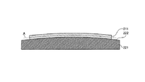
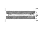
図4は、ステップS101において貼り合わせ部300に搬入される1枚の基板211が基板ホルダ221に保持された状態を示す模式的断面である。基板ホルダ221は、静電チャック、真空チャック等を有して基板211を保持面222に吸着して保持する。   FIG. 4 is a schematic cross section showing a state in which the single substrate 211 carried into the bonding unit 300 in step S101 is held by the substrate holder 221. The substrate holder 221 has an electrostatic chuck, a vacuum chuck, etc., and holds the substrate 211 by attracting it to the holding surface 222.

基板ホルダ221の保持面222は、中央側が高く、周縁が低い湾曲した形状を有する。よって、保持面222に吸着された基板211も、中央側が突出した形状に湾曲する。また、基板ホルダ221が基板211を保持し続けている間は、基板210の凸状の形状が維持される。なお、基板ホルダ221の保持面222の形状は、球面、放物面、円筒面等であってもよい。   The holding surface 222 of the substrate holder 221 has a curved shape with a high center side and a low peripheral edge. Therefore, the substrate 211 adsorbed on the holding surface 222 is also curved into a shape in which the center side protrudes. Further, while the substrate holder 221 continues to hold the substrate 211, the convex shape of the substrate 210 is maintained. The shape of the holding surface 222 of the substrate holder 221 may be a spherical surface, a parabolic surface, a cylindrical surface, or the like.

なお、保持面222に基板211が吸着された場合、湾曲した基板211においては、図中に一点鎖線で示す基板211の厚さ方向の中心部Aに比較して、基板211の図中上面では、基板211の表面が面方向に拡大変形される。また、基板211の図中下面においては、基板211の表面が面方向に縮小変形される。   Note that when the substrate 211 is adsorbed to the holding surface 222, the curved substrate 211 has an upper surface in the drawing of the substrate 211 as compared to the central portion A in the thickness direction of the substrate 211 indicated by a dashed line in the drawing. The surface of the substrate 211 is enlarged and deformed in the surface direction. Further, on the lower surface of the substrate 211 in the drawing, the surface of the substrate 211 is reduced and deformed in the surface direction.

よって、基板211を基板ホルダ221に保持させることにより、基板211の表面に形成された回路領域216の、設計仕様に対する面内の倍率も拡大される。   Therefore, by holding the substrate 211 on the substrate holder 221, the in-plane magnification with respect to the design specification of the circuit region 216 formed on the surface of the substrate 211 is also enlarged.

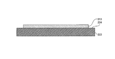
図5は、他の基板213を基板ホルダ223に保持させた状態を示す模式的断面である。基板ホルダ223は、平坦な保持面224と、静電チャック、真空チャック等、基板213を吸着する機能とを有する。基板ホルダ223に吸着して保持された基板213は、保持面224に密着して、保持面224の形状に倣って平坦になる。   FIG. 5 is a schematic cross section showing a state where another substrate 213 is held by the substrate holder 223. The substrate holder 223 has a flat holding surface 224 and a function of attracting the substrate 213 such as an electrostatic chuck or a vacuum chuck. The substrate 213 sucked and held by the substrate holder 223 comes into close contact with the holding surface 224 and becomes flat following the shape of the holding surface 224.

よって、貼り合わせ部300において、図4に示した基板ホルダ221に保持されて凸状に変形した基板211を、図5に示した基板ホルダ223に平坦な状態で保持された基板213に接触させた場合、基板211、213は、中央の一点において接触する。また、基板ホルダ221、223の各々が基板211、213を保持している間は、基板211、213の周縁側の領域は、互いに離れた状態を保つ。   Therefore, in the bonding unit 300, the substrate 211 that is held by the substrate holder 221 shown in FIG. 4 and deformed into a convex shape is brought into contact with the substrate 213 that is held flat by the substrate holder 223 shown in FIG. In this case, the substrates 211 and 213 come into contact at a central point. In addition, while the substrate holders 221 and 223 hold the substrates 211 and 213, the peripheral regions of the substrates 211 and 213 are kept away from each other.

なお、上記の例では、凸状に変形させた基板211と平坦な基板213との組み合わせを例にあげた。しかしながら、例えば、基板211、213を両方とも凸状に変形させた場合、基板211、213を互いに曲率が異なる凸状と凹状に変形させた場合、基板211、213を、中心軸が平行ではない円筒状に変形させた場合も、貼り合わせ部300において、基板211、213を一点で接触させることができる。   In the above example, the combination of the substrate 211 deformed into a convex shape and the flat substrate 213 is taken as an example. However, for example, when both the substrates 211 and 213 are deformed into a convex shape, when the substrates 211 and 213 are deformed into a convex shape and a concave shape having different curvatures, the substrates 211 and 213 are not parallel in the central axis. Even when deformed into a cylindrical shape, the substrates 211 and 213 can be brought into contact with each other at the bonding portion 300.

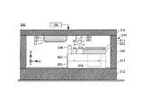
図6は、貼り合わせ部300の構造を示す模式的断面図である。また、図6は、基板211、213および基板ホルダ221、223が搬入された直後の貼り合わせ部300の状態を示す図でもある。貼り合わせ部300は、枠体310、上ステージ322および下ステージ332を備える。   FIG. 6 is a schematic cross-sectional view showing the structure of the bonding unit 300. FIG. 6 is also a diagram illustrating a state of the bonding unit 300 immediately after the substrates 211 and 213 and the substrate holders 221 and 223 are loaded. The bonding unit 300 includes a frame 310, an upper stage 322, and a lower stage 332.

枠体310は、水平な床面301に対して平行な底板312および天板316と、床板に対して垂直な複数の支柱314とを有する。底板312、支柱314および天板316は、貼り合わせ部300の他の部材を収容する直方体の枠体310を形成する。   The frame 310 includes a bottom plate 312 and a top plate 316 that are parallel to the horizontal floor surface 301, and a plurality of columns 314 that are perpendicular to the floor plate. The bottom plate 312, the support column 314, and the top plate 316 form a rectangular frame 310 that accommodates other members of the bonding unit 300.

上ステージ322は、天板316の図中下面に下向きに固定される。上ステージ322は、真空チャック、静電チャック等の保持機能を有して、基板ホルダ221を保持する保持部を形成する。図示の状態において、上ステージ322には、既に、基板211を保持した基板ホルダ221が保持されている。   The upper stage 322 is fixed downward on the lower surface of the top plate 316 in the drawing. The upper stage 322 has a holding function such as a vacuum chuck or an electrostatic chuck, and forms a holding unit that holds the substrate holder 221. In the state shown in the drawing, the upper stage 322 already holds the substrate holder 221 that holds the substrate 211.

下ステージ332は、上ステージ322に対向して配置され、底板312の上面に配されたX方向駆動部331に重ねられたY方向駆動部333の図中上面に搭載される。下ステージ332は、上ステージ322に保持された基板211に対向して、基板213を保持する保持を形成する。図示の状態において、下ステージ332には、既に、基板213を保持した基板ホルダ223を保持する。   The lower stage 332 is disposed opposite to the upper stage 322, and is mounted on the upper surface in the figure of the Y-direction drive unit 333 superimposed on the X-direction drive unit 331 disposed on the upper surface of the bottom plate 312. The lower stage 332 is opposed to the substrate 211 held on the upper stage 322 and forms a holding for holding the substrate 213. In the illustrated state, the lower stage 332 already holds the substrate holder 223 that holds the substrate 213.

なお、図示の状態では、湾曲した保持面222を有する基板ホルダ221が、図中下側に位置する上ステージ322に、平坦な保持面224を有する基板ホルダ223に保持された基板213が、図中下側に位置する下ステージ332に、それぞれ保持されている。しかしながら、上ステージ322および下ステージ332と、基板ホルダ221、223との組み合わせはこれに限らない。また、上ステージ322および下ステージ332の両方に、平坦な基板ホルダ223または湾曲した基板ホルダ221を搬入してもよい。   In the state shown in the drawing, the substrate holder 221 having the curved holding surface 222 is mounted on the upper stage 322 positioned on the lower side in the figure, and the substrate 213 held by the substrate holder 223 having the flat holding surface 224 is shown in FIG. Each is held by a lower stage 332 located on the middle lower side. However, the combination of the upper stage 322 and the lower stage 332 and the substrate holders 221 and 223 is not limited to this. Further, a flat substrate holder 223 or a curved substrate holder 221 may be carried into both the upper stage 322 and the lower stage 332.

貼り合わせ部300において、X方向駆動部331は、底板312と平行に、図中に矢印Xで示す方向に移動する。Y方向駆動部333は、X方向駆動部331上で、底板312と平行に、図中に矢印Yで示す方向に移動する。これら、X方向駆動部331およびY方向駆動部333の動作を組み合わせて、下ステージ332は、底板312と平行に二次元的に移動する。これにより、下ステージ332に搭載した基板213を、上ステージ322に保持した基板211に対して位置合わせできる。   In the bonding unit 300, the X-direction driving unit 331 moves in the direction indicated by the arrow X in the drawing in parallel with the bottom plate 312. The Y direction drive unit 333 moves on the X direction drive unit 331 in parallel with the bottom plate 312 in the direction indicated by the arrow Y in the drawing. The lower stage 332 moves two-dimensionally in parallel with the bottom plate 312 by combining the operations of the X-direction drive unit 331 and the Y-direction drive unit 333. Accordingly, the substrate 213 mounted on the lower stage 332 can be aligned with the substrate 211 held on the upper stage 322.

また、下ステージ332は、底板312に対して垂直に、矢印Zで示す方向に昇降する昇降駆動部338により支持される。下ステージ332は、Y方向駆動部333に対して昇降できる。これにより、貼り合わせ部300は、下ステージ332に搭載した基板213を、上ステージ322に保持した基板213に押し付ける押し付け部の一例である。   The lower stage 332 is supported by an elevating drive unit 338 that elevates in the direction indicated by the arrow Z perpendicular to the bottom plate 312. The lower stage 332 can move up and down with respect to the Y-direction drive unit 333. Accordingly, the bonding unit 300 is an example of a pressing unit that presses the substrate 213 mounted on the lower stage 332 against the substrate 213 held on the upper stage 322.

X方向駆動部331、Y方向駆動部333および昇降駆動部338による下ステージ332の移動量は、干渉計等を用いて精密に計測される。また、X方向駆動部331およびY方向駆動部333は、粗動部と微動部との2段構成としてもよい。これにより、高精度な位置合わせと、高いスループットとを両立させて、下ステージ332に搭載された基板211の移動を、制御精度を低下させることなく高速に貼り合わせできる。   The amount of movement of the lower stage 332 by the X direction drive unit 331, the Y direction drive unit 333, and the elevating drive unit 338 is accurately measured using an interferometer or the like. Further, the X direction drive unit 331 and the Y direction drive unit 333 may have a two-stage configuration of a coarse movement unit and a fine movement unit. Thereby, high-accuracy alignment and high throughput can be achieved at the same time, and the movement of the substrate 211 mounted on the lower stage 332 can be bonded at a high speed without reducing the control accuracy.

Y方向駆動部333には、顕微鏡334および活性化装置326が、それぞれ下ステージ332の側方に更に搭載される。顕微鏡334は、上ステージ322に保持された下向きの基板213の下面を観察できる。活性化装置336は、上ステージ322に保持された基板213の下面を清浄化するプラズマを発生する。   A microscope 334 and an activation device 326 are further mounted on the side of the lower stage 332 in the Y direction driving unit 333. The microscope 334 can observe the lower surface of the downward substrate 213 held by the upper stage 322. The activation device 336 generates plasma that cleans the lower surface of the substrate 213 held by the upper stage 322.

なお、貼り合わせ部300は、底板312に対して垂直な回転軸の回りに下ステージ332を回転させる回転駆動部、および、下ステージ332を揺動させる揺動駆動部を更に備えてもよい。これにより、下ステージ332を上ステージ322に対して平行にすると共に、下ステージ332に保持された基板211を回転させて、基板211、213の位置合わせ精度を向上させることができる。   Note that the bonding unit 300 may further include a rotation driving unit that rotates the lower stage 332 around a rotation axis perpendicular to the bottom plate 312 and a swing driving unit that swings the lower stage 332. Accordingly, the lower stage 332 can be made parallel to the upper stage 322, and the substrate 211 held by the lower stage 332 can be rotated to improve the alignment accuracy of the substrates 211 and 213.

更に、貼り合わせ部300は、一対の顕微鏡324、334と、一対の活性化装置326、336とを有する。一方の顕微鏡324および活性化装置326は、天板316の下面において、上ステージ322の側方に固定される。顕微鏡324は、下ステージ332に保持された基板213の上面を観察できる。活性化装置326は、下ステージ332に保持された基板213の上面を清浄化するプラズマを発生する。   Furthermore, the bonding unit 300 includes a pair of microscopes 324 and 334 and a pair of activation devices 326 and 336. One microscope 324 and the activation device 326 are fixed to the side of the upper stage 322 on the lower surface of the top plate 316. The microscope 324 can observe the upper surface of the substrate 213 held on the lower stage 332. The activation device 326 generates plasma that cleans the upper surface of the substrate 213 held by the lower stage 332.

また、他方の顕微鏡334および活性化装置336は、Y方向駆動部333において、下ステージ332の側方に搭載される。顕微鏡334は、上ステージ322に保持された基板211の下面を観察できる。活性化装置336は、上ステージ322に保持された基板211の下面を清浄化するプラズマを発生する。   The other microscope 334 and the activation device 336 are mounted on the side of the lower stage 332 in the Y-direction drive unit 333. The microscope 334 can observe the lower surface of the substrate 211 held on the upper stage 322. The activation device 336 generates plasma that cleans the lower surface of the substrate 211 held on the upper stage 322.

顕微鏡324、334は、ステップS102において次のような手順で使用できる。制御部150は、図6に示すように、顕微鏡324、334の焦点を相互に合わせることにより、顕微鏡324、334の相対位置を較正する。   The microscopes 324 and 334 can be used in the following procedure in step S102. As shown in FIG. 6, the control unit 150 calibrates the relative positions of the microscopes 324 and 334 by focusing the microscopes 324 and 334 with each other.

制御部150は、図7に示すように、X方向駆動部331およびY方向駆動部333を動作させて、顕微鏡324、334により基板211、213の各々に設けられたアライメントマーク218を検出させる(図3のステップS102)。制御部150は、アライメントマーク218を検出するまでの、X方向駆動部331およびY方向駆動部333による下ステージ332の移動量を把握している。   As shown in FIG. 7, the control unit 150 operates the X direction driving unit 331 and the Y direction driving unit 333 to detect the alignment marks 218 provided on each of the substrates 211 and 213 by the microscopes 324 and 334 ( Step S102 in FIG. 3). The control unit 150 grasps the amount of movement of the lower stage 332 by the X direction driving unit 331 and the Y direction driving unit 333 until the alignment mark 218 is detected.

こうして、相対位置が既知である顕微鏡324、334で基板211、213のアライメントマーク218の位置を検出することにより、基板211、213の相対位置が判る(図3のステップS103)。これにより、重ね合わせる基板211、213を位置合わせする場合には、基板211、213間の表面に沿った面方向の位置ずれ量が所定の値よりも小さくなるように、基板211、213の相対的な移動量および回転量を含む相対移動量を算出すればよい。所定の値は、基板211、213の相互の貼り合わせが完了したときに、基板211,213間に電気的な導通が可能となるずれ量であり、基板211、213にそれぞれ接続部等の構造物が設けられている場合は、構造物同士が少なくとも一部で接触するときのずれ量である。所定の値は、例えば1.0μm以下であり、より好ましくは、0.5μm以下である。基板211,213間の位置ずれが閾値以上になった場合は、接続部同士が接触しない又は適切な電気的導通が得られない、もしくは接合部間に所定の接合強度が得られない。   In this way, the relative positions of the substrates 211 and 213 can be determined by detecting the positions of the alignment marks 218 on the substrates 211 and 213 with the microscopes 324 and 334 whose relative positions are known (step S103 in FIG. 3). Thereby, when aligning the substrates 211 and 213 to be superimposed, the relative positions of the substrates 211 and 213 are set so that the amount of positional deviation in the surface direction along the surface between the substrates 211 and 213 is smaller than a predetermined value. What is necessary is just to calculate the relative movement amount including the general movement amount and the rotation amount. The predetermined value is a shift amount that enables electrical conduction between the substrates 211 and 213 when the bonding of the substrates 211 and 213 is completed. In the case where an object is provided, this is the amount of deviation when the structures contact at least partly. The predetermined value is, for example, 1.0 μm or less, and more preferably 0.5 μm or less. When the positional deviation between the substrates 211 and 213 is equal to or greater than the threshold value, the connection portions do not contact each other, or appropriate electrical conduction cannot be obtained, or a predetermined bonding strength cannot be obtained between the bonding portions.

ただし、貼り合わせ基板230を形成する個々の基板211、213には、個別に歪みが生じている場合がある。このため、基板211、213間の相対的な位置ずれ量が統計的に最小になるように、下ステージ332を平行移動させ、且つ、回転させても、この基板211、213間の歪み量の差によって生じる位置ずれにより、二つの基板211、213のアライメントマーク218の多くが一致しない場合がある。このため、基板211、213がそれぞれ個別に異なる歪みを有する場合は、ステップS106において、相対移動量を計算しても、基板211、213の位置ずれ量が所定の値よりも小さくならない場合がある。   However, the individual substrates 211 and 213 forming the bonded substrate 230 may be individually distorted. For this reason, even if the lower stage 332 is translated and rotated so that the relative positional deviation amount between the substrates 211 and 213 is statistically minimized, the amount of distortion between the substrates 211 and 213 can be reduced. Due to misalignment caused by the difference, many of the alignment marks 218 on the two substrates 211 and 213 may not match. For this reason, if the substrates 211 and 213 have different distortions, the amount of displacement of the substrates 211 and 213 may not be smaller than a predetermined value even if the relative movement amount is calculated in step S106. .

基板211、213に生じる歪みには、基板211、213の反り、撓み等、基板211、213全体で一定の傾向を有する歪みすなわちX方向およびY方向のシフト成分、基板の中心周りの回転成分、および、基板の中心から放射方向に歪む倍率成分と、直交成分と、それら以外の非線形成分とが含まれる。直交成分は、例えば基板の中心を通る線分で分けた二つの領域で線分に沿って互いに反対方向に生じた歪みである。なお、倍率成分には、X方向およびY方向に同じ量だけ変形する等方倍率と、異なる量で変形する非等方倍率とが含まれ、非等方倍率は非線形成分に含まれる。   The distortions generated in the substrates 211 and 213 include warping and bending of the substrates 211 and 213, such as distortions having a certain tendency throughout the substrates 211 and 213, that is, shift components in the X and Y directions, rotation components around the center of the substrate, In addition, a magnification component distorted in the radial direction from the center of the substrate, an orthogonal component, and other nonlinear components are included. The orthogonal component is, for example, distortion generated in opposite directions along the line segment in two regions divided by the line segment passing through the center of the substrate. Note that the magnification component includes an isotropic magnification that is deformed by the same amount in the X direction and the Y direction, and an anisotropic magnification that is deformed by a different amount, and the anisotropic magnification is included in the nonlinear component.

これらの歪みは、基板211、213におけるアライメントマーク218や回路領域216を形成するプロセスにより生じた応力、基板211、213の結晶配向に起因する異方性、スクライブライン212、回路領域216等の配置等に起因する周期的な剛性の変化等により生じる。また、基板211、213を貼り合わせる前に歪みが生じていない場合であっても、接触領域が拡大していく貼り合わせの過程で、既に接触した領域である接触領域と未だ接触していない領域である非接触領域との境界で基板211、213が変形して歪みを生じる場合もある。   These distortions include stress generated by the process of forming the alignment marks 218 and the circuit regions 216 in the substrates 211 and 213, anisotropy due to the crystal orientation of the substrates 211 and 213, the arrangement of the scribe lines 212, the circuit regions 216, and the like. This is caused by a periodic change in rigidity caused by the above. Further, even in the case where no distortion occurs before the substrates 211 and 213 are bonded together, in the process of bonding in which the contact area expands, the area that has not yet been in contact with the contact area that has already been in contact In some cases, the substrates 211 and 213 are deformed and distorted at the boundary with the non-contact region.

このような基板211、213の歪み量の差により生じる基板211、213間の面方向の位置ずれを、少なくとも一方の基板の温度調節により補正する(ステップS105)。つまり、基板211、213の少なくとも一方の温度を調節することによって熱膨張または熱収縮を生じさせることにより、基板211、213の少なくとも一方の全体の大きさを変化させて、他方の基板との位置ずれを補正する。   The positional deviation in the surface direction between the substrates 211 and 213 caused by such a difference in distortion between the substrates 211 and 213 is corrected by adjusting the temperature of at least one of the substrates (step S105). That is, by adjusting the temperature of at least one of the substrates 211 and 213, thermal expansion or thermal contraction is caused, thereby changing the overall size of at least one of the substrates 211 and 213, and the position of the other substrate. Correct the deviation.

温調により位置ずれを補正するとき、制御部150は、位置ずれを解消する補正量を、図示しない算出部に算出させる。算出部は、ステップS103で検出した二つの基板211、213の相対位置すなわち位置ずれ量に基づいて、一方の基板に対する他方の基板の拡大率または縮小率を算出する。このとき、接触領域が拡大する過程で基板211、213の少なくとも一方に生じる歪みによる位置ずれ量を予測または計測し、そのずれ量と、ステップS103で検出した位置ずれ量とに基づいて、拡大率または縮小率を算出してもよい。   When correcting the positional deviation by temperature control, the control unit 150 causes a calculation unit (not shown) to calculate a correction amount for eliminating the positional deviation. The calculation unit calculates an enlargement ratio or a reduction ratio of the other substrate with respect to one substrate based on the relative position of the two substrates 211 and 213 detected in step S103, that is, the amount of displacement. At this time, a displacement amount due to distortion generated in at least one of the substrates 211 and 213 in the process of expanding the contact area is predicted or measured, and the enlargement rate is based on the displacement amount and the displacement amount detected in step S103. Alternatively, the reduction rate may be calculated.

次に、算出部は、補正対象となる基板211、213の熱膨張率を用いて、そのような拡大率または縮小率で基板を拡大または縮小するために求められる目標温度差を算出する。このとき、温度差と補正量との関係を対応付けたテーブルを予め記憶しておき、目標温度差の算出時にこのテーブルを参照してもよい。   Next, the calculation unit calculates a target temperature difference required for enlarging or reducing the substrate at such an enlargement rate or reduction rate using the thermal expansion coefficients of the substrates 211 and 213 to be corrected. At this time, a table in which the relationship between the temperature difference and the correction amount is associated may be stored in advance, and this table may be referred to when calculating the target temperature difference.

尚、温調による補正に加えて、保持面222が湾曲または屈曲した基板ホルダ221に基板211を保持させることにより、基板211の位置ずれを補正することもできる。   In addition to correction by temperature control, the substrate 211 can be held by the substrate holder 221 whose holding surface 222 is curved or bent, so that the positional deviation of the substrate 211 can be corrected.

更に、貼り合わせ部300において、基板211、213を搭載する上ステージ322および下ステージ332の少なくとも一方に、基板211、213を機械的に変形させるアクチュエータを設けて、基板211、213の少なくとも一方を変形させて補正することもできる。これにより、貼り合わせ部300は、基板211、213の位置ずれを、位置ずれの原因となる歪みの成分(線形成分、非線形成分)を問わず補正できる。   Further, in the bonding unit 300, an actuator that mechanically deforms the substrates 211 and 213 is provided on at least one of the upper stage 322 and the lower stage 332 on which the substrates 211 and 213 are mounted, and at least one of the substrates 211 and 213 is attached. It can also be corrected by deformation. Thereby, the bonding unit 300 can correct the positional deviation of the substrates 211 and 213 regardless of the distortion component (linear component or nonlinear component) that causes the positional deviation.

図8は、貼り合わせ部300が基板211、213を活性化する動作(図3のステップS104)を示す。制御部150は、下ステージ332の位置を初期位置にリセットした後に水平に移動させることにより、活性化装置326、336が生成したプラズマを基板211、213の表面に端から順に照射する。これにより、基板211、213のそれぞれの表面が清浄化され、化学的な活性が高くなる。このため、基板211、213は、互いに接触した場合に、自律的に吸着して貼り合わされる状態になる。   FIG. 8 shows an operation in which the bonding unit 300 activates the substrates 211 and 213 (step S104 in FIG. 3). The control unit 150 resets the position of the lower stage 332 to the initial position and then moves it horizontally to irradiate the surfaces of the substrates 211 and 213 sequentially with the plasma generated by the activation devices 326 and 336 from the end. Thereby, the surfaces of the substrates 211 and 213 are cleaned, and the chemical activity is increased. For this reason, when the substrates 211 and 213 come into contact with each other, the substrates 211 and 213 are in an autonomously adsorbed and bonded state.

なお、活性化装置326、336は、顕微鏡324、334の各々から遠ざかる方向にプラズマPを放射する。これにより、プラズマが照射された基板211、213から発生した破片が顕微鏡324を汚染することが防止される。   The activation devices 326 and 336 emit plasma P in a direction away from each of the microscopes 324 and 334. This prevents the fragments generated from the substrates 211 and 213 irradiated with plasma from contaminating the microscope 324.

本実施例では、貼り合わせ部300は、基板211、213を活性化する活性化装置326、326を備えているが、貼り合わせ部300とは別に設けた活性化装置326、326を用いて予め活性化した基板211、213を貼り合わせ部300に搬入することにより、貼り合わせ部300の活性化装置326を省略した構造にすることもできる。   In the present embodiment, the bonding unit 300 includes activation devices 326 and 326 that activate the substrates 211 and 213, but the activation units 326 and 326 provided separately from the bonding unit 300 are used in advance. By bringing the activated substrates 211 and 213 into the bonding unit 300, the activation device 326 of the bonding unit 300 may be omitted.

また、基板211、213の少なくとも一方を活性化するステップS104と、基板211、213のいずれかを温度調節するステップS105とは、順番を入れ換えてもよい。即ち、上記の説明のように、基板211、213を活性化(ステップS104)した後に、基板211、213の少なくとも一方を温度調節(ステップS105)してもよいし、先に基板211、213の少なくとも一方を温度調節した後(ステップS105)に、基板211、213を活性化(ステップS104)してもよい。   The order of step S104 for activating at least one of the substrates 211 and 213 and step S105 for adjusting the temperature of any of the substrates 211 and 213 may be interchanged. That is, as described above, after activating the substrates 211 and 213 (step S104), the temperature of at least one of the substrates 211 and 213 may be adjusted (step S105). After adjusting the temperature of at least one (step S105), the substrates 211 and 213 may be activated (step S104).

図9は、貼り合わせ部300が基板211、213を位置合わせする動作(図3のステップS106)を示す。制御部150は、最初に検出した顕微鏡324、334の相対位置と、ステップS102において検出した基板211、213のアライメントマーク218の位置とに基づいて、下ステージ332を移動させる。このとき、二つの基板211、213の間で互いに対応するアライメントマーク218同士の面方向の位置が一致するように、もしくは、アライメントマーク218同士の相対的な位置ずれ量が前記した所定の値よりも小さくなるように、下ステージ332を移動させてもよい。   FIG. 9 shows an operation (step S106 in FIG. 3) in which the bonding unit 300 aligns the substrates 211 and 213. The control unit 150 moves the lower stage 332 based on the relative position of the microscopes 324 and 334 detected first and the position of the alignment mark 218 on the substrates 211 and 213 detected in step S102. At this time, the positions of the alignment marks 218 corresponding to each other between the two substrates 211 and 213 coincide with each other in the surface direction, or the relative displacement amount between the alignment marks 218 is greater than the predetermined value described above. The lower stage 332 may be moved so as to be smaller.

図10は、図9に示したステップS106の状態における基板211、213の様子を模式的に示す図である。図示のように、それぞれが基板ホルダ221、223を介して上ステージ322および下ステージ332に保持された基板211、213は、互いに位置合わせされた状態で対向する。   FIG. 10 is a diagram schematically showing the state of the substrates 211 and 213 in the state of step S106 shown in FIG. As shown in the drawing, the substrates 211 and 213 held by the upper stage 322 and the lower stage 332 via the substrate holders 221 and 223 respectively face each other while being aligned with each other.

図11は、貼り合わせ部300が下ステージ332に保持された基板213を、上ステージ322に保持された基板211に押し付ける動作(図3のステップS107)を示す。制御部150は、昇降駆動部338を動作させて下ステージ332を上昇させることにより基板211、213を相互に接触させる。   11 shows an operation (step S107 in FIG. 3) in which the bonding unit 300 presses the substrate 213 held on the lower stage 332 against the substrate 211 held on the upper stage 322. The control unit 150 operates the elevating drive unit 338 to raise the lower stage 332 to bring the substrates 211 and 213 into contact with each other.

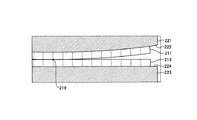
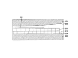
図12は、図10に示したステップS107からステップS108にかけての基板211、213の様子を模式的に示す図である。図示のように、上ステージ322に保持された基板211の中央部が隆起しているので、下ステージ332が上ステージ322に接近すると、まず、基板211、213の中央部が接触する。更に、制御部150が昇降駆動部338の動作を継続することにより、基板211、213の中央部が相互に接触し、図22に示すように、基板211、213に貼り合わせの起点219が形成される。尚、図22から図27は、それぞれ基板211、213の断面図である。また、基板211、213にそれぞれ示されている点線は、基板211、213の断面内における径方向の位置を示しており、基板211、213の中心から径方向に沿って等しい間隔をおき、且つ、二つの基板211、213間で互いに対応する位置に示されている。   FIG. 12 is a diagram schematically showing the state of the substrates 211 and 213 from step S107 to step S108 shown in FIG. As shown in the figure, since the central portion of the substrate 211 held by the upper stage 322 is raised, when the lower stage 332 approaches the upper stage 322, the central portions of the substrates 211 and 213 first come into contact with each other. Further, the control unit 150 continues the operation of the elevating drive unit 338, so that the central portions of the substrates 211 and 213 come into contact with each other, and a starting point 219 for bonding is formed on the substrates 211 and 213 as shown in FIG. Is done. 22 to 27 are sectional views of the substrates 211 and 213, respectively. In addition, dotted lines respectively shown on the substrates 211 and 213 indicate radial positions in the cross sections of the substrates 211 and 213, and are equally spaced from the center of the substrates 211 and 213 along the radial direction, and The two substrates 211 and 213 are shown at positions corresponding to each other.

この状態では、基板ホルダ221は、基板211、213の中央部以外の部分が接触しないように基板211を保持しており、基板211の周縁部は基板213から離れている。   In this state, the substrate holder 221 holds the substrate 211 so that portions other than the central portions of the substrates 211 and 213 do not contact each other, and the peripheral portion of the substrate 211 is separated from the substrate 213.

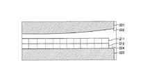
図13は、図3に示したステップS109における基板211、213の状態を示す図である。ステップS109においては、上ステージ322に保持された基板ホルダ221による保持が解除され、基板211が解放される。   FIG. 13 is a diagram showing the state of the substrates 211 and 213 in step S109 shown in FIG. In step S109, the holding by the substrate holder 221 held by the upper stage 322 is released, and the substrate 211 is released.

基板211、213の表面は活性化されているので、一部が密着して貼り合わせの起点219が形成されると、基板211、213同士の分子間力により、隣接する領域が自律的に相互に吸着される。よって、例えば、上ステージ322における基板211の保持を開放することにより、基板211、213の接触領域は、隣接する領域に順次拡がる。   Since the surfaces of the substrates 211 and 213 are activated, when a part of the substrates 211 and 213 are in close contact with each other to form a starting point 219 for bonding, adjacent regions are autonomously mutually connected by the intermolecular force between the substrates 211 and 213. To be adsorbed. Therefore, for example, by releasing the holding of the substrate 211 in the upper stage 322, the contact areas of the substrates 211 and 213 are sequentially expanded to adjacent areas.

換言すれば、上ステージ322において基板211の保持が解除されるまでは、基板211、213の周縁部における接触が規制されている。このため、基板211が上ステージ322に保持されている間は、基板211、213の接触領域の拡大も抑制される。   In other words, the contact at the peripheral edge of the substrates 211 and 213 is restricted until the holding of the substrate 211 in the upper stage 322 is released. For this reason, while the substrate 211 is held by the upper stage 322, the expansion of the contact area of the substrates 211 and 213 is also suppressed.

基板ホルダ221からの基板211の解除により、基板211、213の接触領域が順次拡がっていくボンディングウェイブが発生する。やがて、ボンディングウェイブが基板211、213の周縁部に達したとき、基板211、213は、略全面にわたって貼り合わされる。二つの基板211、213が貼り合わされた状態では、基板211、213が全面的に水素結合のような化学結合により結合されている。こうして、基板211、213は、貼り合わせ基板230を形成する。   The release of the substrate 211 from the substrate holder 221 generates a bonding wave in which the contact areas of the substrates 211 and 213 are sequentially expanded. Eventually, when the bonding wave reaches the peripheral edge of the substrates 211 and 213, the substrates 211 and 213 are bonded over substantially the entire surface. In a state where the two substrates 211 and 213 are bonded together, the substrates 211 and 213 are entirely bonded by chemical bonds such as hydrogen bonds. Thus, the substrates 211 and 213 form a bonded substrate 230.

ステップS107の段階で上ステージ322に保持された状態の基板211は、中央付近が周縁付近よりも突出した状態で保持されている。よって、基板211、213が貼り合わされた領域の拡大は、基板211、213の中央から外縁に向かって拡大する。このため、貼り合わせる前の段階で基板211、213に挟まれていた雰囲気ガス、例えば大気は、基板211、213が貼り合わされた領域の面積が拡がる過程で、基板211、213の内側から外側に向かって押し出され、貼り合わされた基板211、213の間に気泡が残ることが防止される。   The substrate 211 held in the upper stage 322 in the step S107 is held in a state where the vicinity of the center protrudes from the vicinity of the periphery. Therefore, the area where the substrates 211 and 213 are bonded is enlarged from the center of the substrates 211 and 213 toward the outer edge. For this reason, the atmospheric gas sandwiched between the substrates 211 and 213 before the bonding, for example, air, is increased from the inside to the outside of the substrates 211 and 213 in the process of expanding the area of the region where the substrates 211 and 213 are bonded. Air bubbles are prevented from remaining between the substrates 211 and 213 that have been pushed out and bonded together.

基板211、213が重ね合わされる過程で、基板211、213の間から気泡等を円滑に押し出すには、基板211、213の接触が開始された時点で、基板211、213の間に、気泡の移動を妨げない広さを有し、基板211、213の周縁で連続した隙間が形成されていることが好ましい。よって、保持面222が湾曲した基板ホルダ221に吸着させることによる基板211の変形は、ステップS107(図3)で基板213に接触させる段階において、気泡の押し出しが可能な一定の湾曲が残るような変形手順を選択することが好ましい。また、重ね合わせの段階で基板211の湾曲が少なくなることが予測される場合は、気泡を通す間隙を確保する目的で、下ステージ332に保持される基板213を保持する基板ホルダ223として、保持面224が湾曲した基板ホルダを用いてもよい。   In order to smoothly extrude bubbles and the like from between the substrates 211 and 213 in the process of superimposing the substrates 211 and 213, when the contact between the substrates 211 and 213 is started, It is preferable that a gap that does not hinder movement is formed and a continuous gap is formed at the periphery of the substrates 211 and 213. Therefore, the deformation of the substrate 211 caused by the holding surface 222 being attracted to the curved substrate holder 221 leaves a certain curvature that allows the bubbles to be pushed out in the step of contacting the substrate 213 in step S107 (FIG. 3). It is preferable to select a deformation procedure. If it is predicted that the curvature of the substrate 211 is reduced at the stage of superposition, the substrate 211 is held as a substrate holder 223 that holds the substrate 213 held by the lower stage 332 for the purpose of ensuring a gap through which bubbles pass. A substrate holder having a curved surface 224 may be used.

また、上記の例では、ステップS109に、上ステージ322に保持された基板211の保持を解除した。しかしながら、同ステップにおいては、下ステージ332による保持を解除してもよいし、両方のステージにおいて基板211、213の保持を解除してもよい。   In the above example, the holding of the substrate 211 held on the upper stage 322 is released in step S109. However, in the same step, the holding by the lower stage 332 may be released, or the holding of the substrates 211 and 213 may be released in both stages.

ただし、保持を解除した基板211は、基板ホルダ221からの吸着による歪みの補正も解除されることになる。よって、ステップS109において基板の保持を解除する場合は、基板間の位置ずれの原因となる面方向の歪みや反りの変形量が相対的に少なく、補正量がより小さい方の基板211、213の保持を解除することが好ましい。   However, the correction of the distortion due to the suction from the substrate holder 221 is also released from the substrate 211 whose holding has been released. Therefore, when releasing the holding of the substrate in step S109, the deformation of the surface direction distortion or warpage that causes the positional deviation between the substrates is relatively small, and the correction amount of the substrate 211, 213 with the smaller correction amount is set. It is preferable to release the holding.

また、ステップS109において基板211の保持を解除するタイミングは、ステップS108において判断される貼り合わせの起点219が形成されたか否かに依存する。換言すれば、保持部としての基板ホルダ221は、基板211、213の一部に貼り合された領域が形成されるまでの期間、基板211、213を保持し続ける。また、貼り合わせ部300は、制御部150の制御の下に、基板211、213の一部に貼り合された領域が形成されるまでの期間、基板211、213を押し付け続ける。   Further, the timing of releasing the holding of the substrate 211 in step S109 depends on whether or not the bonding start point 219 determined in step S108 has been formed. In other words, the substrate holder 221 as a holding unit continues to hold the substrates 211 and 213 until a region bonded to a part of the substrates 211 and 213 is formed. In addition, the bonding unit 300 continues to press the substrates 211 and 213 until a region bonded to a part of the substrates 211 and 213 is formed under the control of the control unit 150.

ステップS109において基板211の保持を解除するタイミングは、ステップS107の後に基板211、213に形成される貼り合わせの起点219を検知して、検知結果に基づいて決定できる。貼り合わせの起点検知は、例えば、一部または全部が透明なステージを用いて、基板211、213を透過する波長で基板211、213を光学的に観察してもよい。また、下ステージ332を上昇させる昇降駆動部338の機械的負荷または電気的な負荷の変動を検出して、起点219の形成を判断する判断部を制御部150に実装し、この判断部による判断結果に基づいて起点219が形成されたことを判断してもよい。   The timing of releasing the holding of the substrate 211 in step S109 can be determined based on the detection result by detecting the bonding start point 219 formed on the substrates 211 and 213 after step S107. For detection of the starting point of bonding, for example, the substrates 211 and 213 may be optically observed at a wavelength that transmits the substrates 211 and 213 using a stage partially or entirely transparent. In addition, a determination unit that detects the mechanical load or the electrical load of the elevating drive unit 338 that raises the lower stage 332 and determines the formation of the starting point 219 is mounted on the control unit 150, and the determination by the determination unit is performed. It may be determined that the starting point 219 is formed based on the result.

また、貼り合わせ部300における判断部としての制御部150は、ステップS108において、基板211、213の一部を押し付け始めてから、予め定めた時間が経過した場合に、基板211、213の一部が貼り合わされて起点219が形成されたと判断してもよい。判断の閾値となる時間は、例えば、貼り合わせる基板211、213と同じ仕様の基板を貼り合わせて、起点219が確実に形成される時間を予め決定しておいてもよい。   In addition, in step S108, the control unit 150 serving as the determination unit in the bonding unit 300 starts pressing part of the substrates 211 and 213, and when a predetermined time has elapsed, It may be determined that the starting point 219 is formed by pasting. The determination threshold time may be determined in advance, for example, by bonding substrates having the same specifications as the substrates 211 and 213 to be bonded together to reliably form the starting point 219.

また、制御部150が、貼り合わせの起点219が形成されたと判断する時間は、基板211、213のロット毎または基板の種類毎に変更してもよい。時間の変更は、制御部150を通じて、貼り合わせの対象毎に手動で変更してもよいし、貼り合わせる基板211、213の種類と関連付けて保存した情報を参照して自動的に設定してもよい。   The time for which the control unit 150 determines that the bonding start point 219 has been formed may be changed for each lot of the substrates 211 and 213 or for each type of substrate. The change of time may be manually changed for each object to be bonded through the control unit 150, or may be automatically set with reference to information stored in association with the type of substrates 211 and 213 to be bonded. Good.

なお、貼り合わせ部300においては、前記したように算出した温度差に基づいて、貼り合わせる基板211、213の少なくとも一方の温度を調節することにより、基板211、213の倍率差による位置ずれを補正する。   Note that in the bonding unit 300, the positional deviation due to the magnification difference between the substrates 211 and 213 is corrected by adjusting the temperature of at least one of the substrates 211 and 213 to be bonded based on the temperature difference calculated as described above. To do.

貼り合わされる基板211、213に温度差を設けた場合、基板211、213において起点219を形成する過程および接触領域が拡大していく過程で、基板211、213の接触領域において、基板211、213のうち温度が高い方の基板から温度が低い方の基板へと熱が伝わり、基板211、213の間の温度差が設定した温度差からずれる。温度が低い基板の接触領域から非接触領域に当該基板内を熱が伝わることにより非接触領域の温度が変化し、図23に点線で示すように、非接触領域に変形が生じる。非接触領域に熱変形が生じると、図24に示すように、両基板211、213の非接触領域同士を貼り合わせたときに、領域231において基板211、213間に位置ずれが生じる。この位置ずれは、図24において、基板211、213間で互いに対応する点線の位置がずれていることで示されている。この変形には、基板211、213の面方向に沿った伸縮変形や反り変形が含まれる。   When a temperature difference is provided between the substrates 211 and 213 to be bonded, in the process of forming the starting point 219 in the substrates 211 and 213 and the process of expanding the contact area, the substrates 211 and 213 are in contact areas of the substrates 211 and 213. Heat is transferred from the substrate having the higher temperature to the substrate having the lower temperature, and the temperature difference between the substrates 211 and 213 deviates from the set temperature difference. The heat in the substrate is transferred from the contact region of the substrate having a low temperature to the non-contact region, so that the temperature of the non-contact region is changed, and the non-contact region is deformed as indicated by a dotted line in FIG. When thermal deformation occurs in the non-contact region, as shown in FIG. 24, when the non-contact regions of both the substrates 211 and 213 are bonded together, a positional deviation occurs between the substrates 211 and 213 in the region 231. This positional deviation is shown in FIG. 24 by the fact that the positions of the dotted lines corresponding to each other between the substrates 211 and 213 are shifted. This deformation includes expansion and contraction deformation and warpage deformation along the surface direction of the substrates 211 and 213.

そこで、基板211、213の一部が接触して接触領域が形成されて、その一部における211、213温度差が小さくなり始めてから、その温度差が予め定めた許容範囲の値よりも小さくなる前に、すなわち、接触領域からの熱伝達により二つの基板211、213の非接触領域の温度が変化して非接触領域の間の温度差が所定の範囲を超える前に、すなわち、基板211、213の少なくとも一方の非接触領域に変形が生じることにより、非接触領域の間に閾値以上の位置ずれが生じる前に、基板211、213の一方の保持を解除して、接触領域の拡大を開始させる。拡大する接触領域の外周にはボンディングウェイブが発生して、基板211、213の接触領域が拡がっていく。   Therefore, after a part of the substrates 211 and 213 come into contact with each other to form a contact region and the temperature difference 211 and 213 in the part starts to decrease, the temperature difference becomes smaller than a predetermined allowable range value. Before, that is, before the temperature difference between the non-contact areas exceeds the predetermined range due to the heat transfer from the contact areas, the temperature of the non-contact areas of the two substrates 211 and 213 exceeds the predetermined range, that is, the substrates 211, When deformation occurs in at least one of the non-contact areas of 213, the holding of one of the substrates 211 and 213 is released and the enlargement of the contact area is started before a positional shift exceeding the threshold occurs between the non-contact areas. Let A bonding wave is generated on the outer periphery of the expanding contact area, and the contact areas of the substrates 211 and 213 are expanded.

ここで、基板211、213において接触領域となった部分では、基板211、213間の温度差が減少しても、基板211、213相互の機械的な結合により、ずれの発生または拡大は抑制される。一方、基板211、213が未だ接触していないボンディングウェイブの外側になる基板211、213の非接触領域では、隣接する接触領域において接触した基板211、213の間の熱伝導により基板211、213間の温度差が減少する。このため、基板211、213の温度差が予め設定した許容範囲よりも多く減少すると、基板211、213にずれが生じる。   Here, in the part which became the contact region in the substrates 211 and 213, even if the temperature difference between the substrates 211 and 213 decreases, the occurrence or expansion of the shift is suppressed by the mechanical coupling between the substrates 211 and 213. The On the other hand, in the non-contact region of the substrates 211 and 213 that are outside the bonding wave where the substrates 211 and 213 are not yet in contact, the heat transfer between the substrates 211 and 213 that are in contact with each other in the adjacent contact region causes The temperature difference of decreases. For this reason, if the temperature difference between the substrates 211 and 213 decreases more than a preset allowable range, the substrates 211 and 213 are displaced.

なお、非接触領域における温度差の変化は、基板211、213における貼り合わせ面の平坦性等の状態、接触領域の拡大が開始されるまでに基板211、213の接触状態が継続する時間、基板211、213の厚さ、熱伝導率等の諸特性に基づいて予測できる。よって、上記の適切な許容範囲を予め設定することができる。   Note that the change in temperature difference in the non-contact region includes the state of the flatness of the bonding surfaces in the substrates 211 and 213, the time that the contact state of the substrates 211 and 213 continues until the expansion of the contact region is started, Prediction can be made based on various properties such as thicknesses 211 and 213 and thermal conductivity. Therefore, the appropriate allowable range can be set in advance.

また、上記の基板211、213の間の温度差は、互いに接触する面において生じていればよく、基板211、213全体に温度差が生じていなくてもよい。よって、基板211、213の接触を検出してから温度差が予め定めた許容範囲の値よりも小さくなる前に接触領域の拡大を開始させることにより、図25に示すように、実効的な基板211、213の温度差を維持して、位置ずれを生じることなく基板211、213を貼り合わせることができる。   Further, the temperature difference between the substrates 211 and 213 may be generated on the surfaces in contact with each other, and the temperature difference may not be generated on the entire substrates 211 and 213. Therefore, by detecting the contact between the substrates 211 and 213 and starting the expansion of the contact area before the temperature difference becomes smaller than a predetermined allowable range, an effective substrate is obtained as shown in FIG. The substrates 211 and 213 can be bonded together while maintaining the temperature difference between 211 and 213 without causing a positional shift.

図14は、温度差を有する基板211、213を貼り合わせる場合に貼り合わせ基板230に生じた接合後の平均倍率と非線形ずれ量の一例を示すグラフである。平均倍率は、貼り合わされた基板211、213の面内の複数箇所における基板211、213間の倍率差の平均である。非線形ずれ量は、基板211、213の接触から貼り合わせ完了までの過程で生じた非線形成分の歪みによる基板211、213間のずれ量である。   FIG. 14 is a graph showing an example of the average magnification and the amount of non-linear deviation after bonding generated in the bonded substrate 230 when the substrates 211 and 213 having a temperature difference are bonded together. The average magnification is an average of the magnification differences between the substrates 211 and 213 at a plurality of locations in the plane of the bonded substrates 211 and 213. The amount of non-linear deviation is the amount of deviation between the substrates 211 and 213 due to the distortion of the non-linear component generated in the process from the contact of the substrates 211 and 213 to the completion of bonding.

図示の例では、貼り合わせ開始の当初、倍率差および非線形ずれ量が生じていない基板211、213に5℃の温度差を形成し、二つの基板211、213のうち一方の基板に対して他方に正の倍率変形を生じさせている。グラフの横軸には、ステップS107(図3参照)に基板211、213の一部を接触させてから、ステップS109(図3参照)に基板211、213の保持を解除するまでの待機時間が示される。平均倍率および非線形ずれ量のそれぞれのグラフの変化率は、貼り合わされる二つの基板211、213の熱伝達率によって変化する。   In the example shown in the drawing, a temperature difference of 5 ° C. is formed on the substrates 211 and 213 in which the magnification difference and the non-linear deviation amount are not generated at the beginning of the bonding, and the other of the two substrates 211 and 213 is the other. Causes a positive magnification deformation. On the horizontal axis of the graph, a waiting time from when a part of the substrates 211 and 213 is brought into contact with step S107 (see FIG. 3) until the holding of the substrates 211 and 213 is released at step S109 (see FIG. 3). Indicated. The rate of change of each graph of the average magnification and the amount of nonlinear deviation varies depending on the heat transfer rates of the two substrates 211 and 213 to be bonded together.

図示のグラフには、5℃の温度差を設定した基板211、213を貼り合わせるにあたって、基板211、213の一部を接触させてから、1秒後、2秒後、5秒後および10秒後に一方の基板211の保持を解除して基板211、213全体を貼り合わせた場合の、貼り合わせ基板230の平均倍率と、非線形ずれ量とをプロットした。   In the illustrated graph, when the substrates 211 and 213 set with a temperature difference of 5 ° C. are bonded together, 1 second, 2 seconds, 5 seconds, and 10 seconds after contacting a part of the substrates 211 and 213 The average magnification of the bonded substrate 230 and the amount of non-linear deviation when the holding of one substrate 211 was later released and the substrates 211 and 213 were bonded together were plotted.

図示のように、基板211の保持を解除するまでの待機時間すなわち基板211の一部を基板213に接触させた状態を維持した時間が長くなるほど、基板211、213を貼り合わせた後の平均倍率は減少する。これは、基板211、213を押し付けた状態の待機時間が長くなるにつれて、基板211、213の温度が高い方から低い方へと熱が伝達され、二つの基板211、213の温度がほぼ等しくなることにより、二つの基板211、213の熱による変形量もほぼ等しくなるためであると推測される。よって、温度差による倍率補正が施された基板を他の基板に貼り合わせるとき、すなわち、温度差により倍率差が所定の値よりも小さくなっている二つの基板を貼り合わせるときに、待機時間が長くなるほど、貼り合わせ前に一方の基板に生じさせた変形が基板間の熱伝達により解消されて倍率差が大きくなる。   As shown in the figure, the average magnification after bonding the substrates 211 and 213 increases as the standby time until the holding of the substrate 211 is released, that is, the time during which a part of the substrate 211 is kept in contact with the substrate 213 becomes longer. Decrease. This is because heat is transferred from the higher temperature to the lower temperature of the substrates 211 and 213 as the standby time in a state in which the substrates 211 and 213 are pressed is increased, and the temperatures of the two substrates 211 and 213 become substantially equal. Thus, it is assumed that the deformation amounts due to heat of the two substrates 211 and 213 are almost equal. Therefore, when a substrate subjected to magnification correction due to a temperature difference is bonded to another substrate, that is, when two substrates having a magnification difference smaller than a predetermined value due to a temperature difference are bonded, As the length increases, the deformation caused on one of the substrates before bonding is eliminated by heat transfer between the substrates, and the magnification difference increases.

一方、時間の経過と共に、互いに接触した二つの基板211、213の一方から他方への熱の伝達量が大きくなるので、基板211の保持を解除するまでの待機時間が長くなるほど、基板211、213を貼り合わせた後の非線形ずれ量も大きくなる。よって、温度差による倍率補正と、非線形ずれ量の抑制という観点からは、基板211の保持を解除するまでの待機時間は、短い方が好ましいと考えられる。また、二つの基板211、213に設定する温度差が大きいほど熱伝達が早いため、補正量が大きくなるに従って、待機時間を短くすることが好ましく、補正精度が高いほど待機時間を短くすることが好ましい。   On the other hand, since the amount of heat transferred from one of the two substrates 211 and 213 in contact with each other to the other increases with time, the longer the waiting time until the holding of the substrate 211 is released, the longer the substrates 211 and 213 are. The amount of non-linear deviation after bonding is also increased. Therefore, it is considered that a shorter waiting time until the holding of the substrate 211 is released is preferable from the viewpoint of magnification correction based on the temperature difference and suppression of the non-linear deviation amount. In addition, since the heat transfer is faster as the temperature difference set between the two substrates 211 and 213 is larger, it is preferable to shorten the standby time as the correction amount increases, and to shorten the standby time as the correction accuracy is higher. preferable.

ただし、ステップS107(図3参照)において、貼り合わせの起点219が形成される前すなわち二つの基板211、213間に所定の結合力が確保される前に一方の基板211の保持を解除した場合、貼り合わせ過程で基板211、213間に位置ずれが生じる。よって、起点219を形成する観点では、所定の結合力が生じるまで待機時間を確保する必要がある。従って、基板211、213を貼り合わせる場合は、基板211、213に起点219が形成された後であって、且つ、基板211、213の温度差が予め定められた閾値よりも小さくなる前すなわち基板211、213の少なくとも一方に変形が生じることにより基板211、213間の倍率差および非線形ずれ量を含むずれ量が閾値以上になる前に、一方の基板211を解放して接触領域の拡大を開始することが好ましい。   However, in step S107 (see FIG. 3), when the holding of one substrate 211 is released before the bonding starting point 219 is formed, that is, before a predetermined bonding force is secured between the two substrates 211 and 213. In the bonding process, a positional deviation occurs between the substrates 211 and 213. Therefore, from the viewpoint of forming the starting point 219, it is necessary to ensure a waiting time until a predetermined binding force is generated. Therefore, when the substrates 211 and 213 are bonded together, after the starting point 219 is formed on the substrates 211 and 213 and before the temperature difference between the substrates 211 and 213 becomes smaller than a predetermined threshold, that is, the substrate Before the displacement amount including the magnification difference between the substrates 211 and 213 and the nonlinear displacement amount exceeds a threshold due to deformation in at least one of 211 and 213, the one substrate 211 is released to start expanding the contact area. It is preferable to do.

上記の接触領域の拡大を開始するときのずれ量の閾値は、基板211、213の相互の貼り合わせが完了したときに、基板211,213間に電気的な導通が可能となるずれ量であり、基板211、213にそれぞれ接続部等の構造物が設けられている場合は、構造物同士が少なくとも一部で接触するときのずれ量である。基板211,213間の位置ずれが閾値以上になった場合は、接続部同士が接触しない又は適切な電気的導通が得られない、もしくは接合部間に所定の接合強度が得られない。つまり、閾値は、基板211、213の貼り合わせが完了した際の位置ずれの許容範囲の最大値すなわち許容値であり、例えば基板211、213の種類、接合プロセス、および、基板貼り合わせ装置100毎に、予め定められている。例えば、基板211、213間の温度差を小さくして4℃に設定することにより、平均倍率を小さくすることによって、待機時間が1秒で非線形ずれ量を小さくすることができる。   The threshold value of the shift amount when starting the expansion of the contact area is a shift amount that enables electrical conduction between the substrates 211 and 213 when the bonding of the substrates 211 and 213 is completed. In the case where structures such as connection portions are provided on the substrates 211 and 213, the amount of displacement when the structures are in contact with each other at least partially. When the positional deviation between the substrates 211 and 213 is equal to or greater than the threshold value, the connection portions do not contact each other, or appropriate electrical conduction cannot be obtained, or a predetermined bonding strength cannot be obtained between the bonding portions. In other words, the threshold value is the maximum value of the allowable range of misalignment when the bonding of the substrates 211 and 213 is completed, that is, the allowable value. For example, the type of the substrates 211 and 213, the bonding process, and the substrate bonding apparatus 100 Are predetermined. For example, by reducing the temperature difference between the substrates 211 and 213 and setting the temperature difference to 4 ° C., the average magnification can be reduced to reduce the nonlinear deviation amount in one second.

貼り合わせる基板211、213に貼り合わせの起点219が形成されるに足る待機時間を予め測定または算出して、当該待機時間の間に減少する基板211、213の温度差を見込んで、基板211、213の貼り合わせを開始する時点での温度差を、二つの基板211、213のずれ量の補正に必要となる目標温度差よりも大きくしておいてもよい。この場合、基板211、213に当初設定される温度差は、例えば、待機時間後にステップS109を開始した時点で、基板211、213の倍率が補償される温度差となるように決定してもよい。この場合、基板211、213の接触により温度差が、目標温度差を含む所定の範囲を下回る前に、接触領域の拡大を開始することが好ましい。   By measuring or calculating in advance a waiting time sufficient to form the bonding starting point 219 on the substrates 211 and 213 to be bonded, and taking into account the temperature difference between the substrates 211 and 213 that decreases during the waiting time, the substrate 211, The temperature difference at the time of starting the bonding of 213 may be set larger than the target temperature difference required for correcting the shift amount between the two substrates 211 and 213. In this case, the temperature difference initially set on the substrates 211 and 213 may be determined to be a temperature difference at which the magnification of the substrates 211 and 213 is compensated when, for example, step S109 is started after the standby time. . In this case, it is preferable to start expanding the contact area before the temperature difference falls below a predetermined range including the target temperature difference due to the contact between the substrates 211 and 213.

また、基板211、213の温度差による倍率補正の観点からすると、基板211、213の貼り合わせが完了した時点、即ち、基板211、213に形成され起点219からの接触領域の拡大が終了した時点で、基板211、213間の温度差が所定の範囲内に入るように、予め温度差を大きく設定しておいてもよい。所定の範囲は、二つの基板211、213の前記した位置ずれ量の許容範囲に対応して設定され、温度差が所定の範囲を超えると、基板211、213の接続部同士が接触しない又は適切な電気的接続を得ることができない、もしくは接合部間に所定の接合強度が得られない。設定する温度差、および、一方の基板の保持を解除するタイミングは、後述するように、接触領域の拡大中に基板211、213間の伝熱により生じる温度の変化量を考慮して、設定される。   Further, from the viewpoint of magnification correction due to the temperature difference between the substrates 211 and 213, when the bonding of the substrates 211 and 213 is completed, that is, when the expansion of the contact area formed on the substrates 211 and 213 from the starting point 219 is completed. Thus, the temperature difference may be set in advance so that the temperature difference between the substrates 211 and 213 falls within a predetermined range. The predetermined range is set corresponding to the allowable range of the positional deviation amount of the two substrates 211 and 213, and when the temperature difference exceeds the predetermined range, the connecting portions of the substrates 211 and 213 are not in contact with each other. Can not be obtained, or a predetermined bonding strength cannot be obtained between the bonding portions. The temperature difference to be set and the timing for releasing the holding of one substrate are set in consideration of the amount of change in temperature caused by heat transfer between the substrates 211 and 213 during expansion of the contact area, as will be described later. The

図15は、貼り合わせ部300において基板211、213の温度調節をする温度調節部の一例を示す模式図である。前記したように、起点形成時に二つの基板211、213の接触により熱伝達が生じ、基板211、213間の温度差が設定した温度差よりも小さくなる。この現象は、基板211、213の接触領域が拡大する過程でも同様に生じる。このため、温度調節部は、基板211、213が互いに接触してから貼り合わせが完了するまでの間において、温度差を付けた基板211、213の少なくとも一方の基板と外部との熱の交流を制御し、基板211、213の温度差を所定の範囲内に維持する。外部には、他方の基板、および、基板211、213の雰囲気ガス等が含まれる。   FIG. 15 is a schematic diagram illustrating an example of a temperature adjustment unit that adjusts the temperature of the substrates 211 and 213 in the bonding unit 300. As described above, heat transfer occurs due to the contact between the two substrates 211 and 213 when the starting point is formed, and the temperature difference between the substrates 211 and 213 becomes smaller than the set temperature difference. This phenomenon also occurs in the process where the contact area between the substrates 211 and 213 is enlarged. For this reason, the temperature adjustment unit exchanges heat between at least one of the substrates 211 and 213 having a temperature difference and the outside between the contact between the substrates 211 and 213 and the completion of bonding. And the temperature difference between the substrates 211 and 213 is maintained within a predetermined range. The outside includes the other substrate, the atmospheric gas of the substrates 211 and 213, and the like.

図15に示す例では、温度調節部は、下ステージ332に内蔵された複数のヒータ339を有する。複数のヒータ339は、接触領域が拡大していく方向すなわち下ステージ332の径方向に分割して設けられ、制御部150により個別に発熱量が調節される。複数のヒータ339は、基板213を保持する基板ホルダ223を加熱して温度調節することにより、基板ホルダ223に保持された基板213を複数のヒータ339に対応する領域毎に温度調節する。   In the example illustrated in FIG. 15, the temperature adjustment unit includes a plurality of heaters 339 built in the lower stage 332. The plurality of heaters 339 are provided separately in the direction in which the contact area expands, that is, in the radial direction of the lower stage 332, and the amount of heat generated is individually adjusted by the control unit 150. The plurality of heaters 339 adjust the temperature of the substrate 213 held by the substrate holder 223 for each region corresponding to the plurality of heaters 339 by heating the substrate holder 223 holding the substrate 213 and adjusting the temperature.

基板213を温調するとき、基板ホルダ223への基板213の保持を一旦解除し、温調により基板213を変形させた後、図26に示すように、基板213を基板ホルダ223に再度保持する。これにより、基板213の倍率を含む歪み量を、基板211の歪み量に応じて調整して、図27に示すように、位置ずれの抑制された貼り合わせ基板230を作製できる。ヒータ339としては、抵抗加熱ヒータの他、ペルチェ効果素子、誘導加熱装置、赤外線照射装置等、他の加熱装置を用いてもよい。   When the temperature of the substrate 213 is adjusted, the holding of the substrate 213 to the substrate holder 223 is once released, the substrate 213 is deformed by the temperature adjustment, and then the substrate 213 is held again on the substrate holder 223 as shown in FIG. . Thus, the amount of strain including the magnification of the substrate 213 is adjusted according to the amount of strain of the substrate 211, and as shown in FIG. 27, a bonded substrate 230 with suppressed displacement can be manufactured. As the heater 339, other heating devices such as a Peltier effect element, an induction heating device, and an infrared irradiation device may be used in addition to the resistance heater.

制御部150は、二つの基板211、213の接触領域が拡大していく過程において、接触領域と非接触領域との境界の移動位置すなわち基板211、213が接触して熱伝達が行われる位置に応じて、その位置に対応するヒータ339の温度を順に調整する。ヒータ339の温度は、少なくとも熱伝達により基板213の温度が下がった分を上昇させて、二つの基板211、213の温度差が所定の範囲内で維持するように設定される。   In the process of expanding the contact area between the two substrates 211 and 213, the controller 150 moves the boundary between the contact area and the non-contact area, that is, a position where the substrates 211 and 213 come into contact with each other and heat transfer is performed. Accordingly, the temperature of the heater 339 corresponding to the position is sequentially adjusted. The temperature of the heater 339 is set so that the temperature difference between the two substrates 211 and 213 is maintained within a predetermined range by increasing at least the amount by which the temperature of the substrate 213 has decreased due to heat transfer.

具体的には、基板213の非接触領域のうち境界に隣接する部分の熱が基板213内を伝わって基板213の接触領域から基板211に伝わるため、当該部分と当該部分に対応する基板211の部分との間の温度差が予め設定された所定の範囲内に入るように、当該部分に対応するヒータ339を制御する。境界の移動に伴って、基板213の中心から周縁部に向けて、複数のヒータ339の制御を順に行う。これにより、基板211、213の非接触領域の互いに対応する部分が互いに接触するまで、当該部分の間の温度差が所定の範囲内に維持される。つまり、接触領域の相互の接触時の熱交換によって非接触領域の互いに対応する部分の間の温度差が所定の範囲外になることが抑制される。接触領域と非接触領域との境界の位置を検出する検出部を設け、この検出部の検出結果に基づいて制御すべきヒータ339を決定してもよい。   Specifically, the heat of the portion adjacent to the boundary in the non-contact region of the substrate 213 is transmitted through the substrate 213 and is transmitted from the contact region of the substrate 213 to the substrate 211, so that the portion and the substrate 211 corresponding to the portion are in contact. The heater 339 corresponding to the part is controlled so that the temperature difference with the part falls within a predetermined range set in advance. As the boundary moves, the plurality of heaters 339 are sequentially controlled from the center of the substrate 213 toward the peripheral edge. Accordingly, the temperature difference between the corresponding portions of the non-contact regions of the substrates 211 and 213 is maintained within a predetermined range until the portions corresponding to each other come into contact with each other. That is, it is suppressed that the temperature difference between the parts corresponding to each other in the non-contact area is outside a predetermined range due to heat exchange at the time of contact of the contact areas. A detection unit that detects the position of the boundary between the contact region and the non-contact region may be provided, and the heater 339 to be controlled may be determined based on the detection result of the detection unit.

尚、基板ホルダ223への基板213の保持力が、温度低下による基板213の熱変形力よりも大きい場合は、接触領域の境界の位置変化に応じたヒータ339の制御を不要とすることができる。   When the holding force of the substrate 213 to the substrate holder 223 is larger than the thermal deformation force of the substrate 213 due to a temperature drop, it is unnecessary to control the heater 339 according to the change in the position of the boundary of the contact region. .

また、図示の例では、温度調節部は、上ステージ322に保持された基板ホルダ221に形成された複数の通気孔225を有する。基板ホルダ221の通気孔225は、上ステージ322に設けられた給気孔に連通している。温度調節部は、基板211の保持を解除するとき又は解除した後に、基板211に向かって気体を噴射して吹きつける。このとき、接触領域と非接触領域との境界の移動位置に応じて、その位置に対応する通気孔225から基板211に気体を噴射する。   In the illustrated example, the temperature adjustment unit has a plurality of air holes 225 formed in the substrate holder 221 held by the upper stage 322. A vent hole 225 of the substrate holder 221 communicates with an air supply hole provided in the upper stage 322. The temperature adjusting unit sprays and blows gas toward the substrate 211 when or after releasing the holding of the substrate 211. At this time, according to the movement position of the boundary between the contact area and the non-contact area, gas is injected from the vent hole 225 corresponding to the position to the substrate 211.

また、温度調節部は、通気孔225を通して噴出する気体の温度を調節する。図示の例のように、基板211の歪み量を基準にして基板213が加熱により変形されている場合、基板213からの熱伝達により基板211が変形するため、気体の温度は、その変形により基板211、213間に生じるずれが抑制される温度に設定される。   Further, the temperature adjusting unit adjusts the temperature of the gas ejected through the vent hole 225. As shown in the example, when the substrate 213 is deformed by heating with reference to the amount of distortion of the substrate 211, the substrate 211 is deformed by heat transfer from the substrate 213. It is set to a temperature at which the deviation between 211 and 213 is suppressed.

具体的には、基板213から接触領域を通して基板211に伝わった熱が基板211内を伝わって基板211の非接触領域のうち境界に隣接する部分に伝わるため、当該部分と当該部分に対応する基板213の部分との間の温度差が予め設定された所定の範囲内に入るように、当該部分に対応する通気孔225からの気体の温度を制御する。   Specifically, since heat transferred from the substrate 213 to the substrate 211 through the contact region is transmitted through the substrate 211 to a portion adjacent to the boundary in the non-contact region of the substrate 211, the portion and the substrate corresponding to the portion. The temperature of the gas from the vent hole 225 corresponding to the portion is controlled so that the temperature difference with the portion 213 falls within a predetermined range set in advance.

図示の状態は、図3におけるステップS109の直後の状態を示し、基板211、213は、中央部において貼り合わされているが、周縁は未だ貼り合わされていない。この状態で、通気孔225から図中上側の基板211に向かって噴射する気体の温度を調節することにより、保持を解除した後の基板211の温度を能動的に調節しつつ、基板211、213の貼り合わせを進行させることができる。   The state shown in FIG. 3 shows a state immediately after step S109 in FIG. 3, and the substrates 211 and 213 are bonded at the central portion, but the peripheral edge is not yet bonded. In this state, by adjusting the temperature of the gas injected from the vent hole 225 toward the upper substrate 211 in the figure, the temperature of the substrate 211 after releasing the holding is actively adjusted, while the substrates 211 and 213 are being adjusted. Can be progressed.

このような温度調節部による温調により、二つの基板211、213の少なくとも一方において、接触領域における熱交換により、まだ接触していない非接触領域の温度が変化することが抑制される。   Such temperature control by the temperature control unit suppresses a change in the temperature of the non-contact region that is not yet in contact due to heat exchange in the contact region in at least one of the two substrates 211 and 213.

上記した例において、基板211の領域毎に補正量が異なる場合は、各領域に対応する通気孔225から噴射される気体の温度、および、ヒータ339の温度の少なくとも一つを、その領域の補正量に応じた温度に設定してもよい。   In the above-described example, when the correction amount is different for each region of the substrate 211, at least one of the temperature of the gas injected from the vent hole 225 corresponding to each region and the temperature of the heater 339 is corrected for that region. You may set to the temperature according to quantity.

また、例えば赤外線温度センサのような温度センサ等の検出部の検出結果に基づいて、起点形成の過程および接触領域が拡大する過程で変化する基板211、213の温度をリアルタイムで検出または予測し、検出または予測した温度に基づいて、噴射される気体の温度およびヒータ339の温度を調整してもよい。   Further, based on the detection result of a detection unit such as a temperature sensor such as an infrared temperature sensor, the temperatures of the substrates 211 and 213 that change in the process of forming the starting point and the process of expanding the contact area are detected or predicted in real time, The temperature of the injected gas and the temperature of the heater 339 may be adjusted based on the detected or predicted temperature.

また、上記した例では、接触領域の拡大の進行に応じてヒータ339および気体の温度を順に調整する例を示したが、これに代えて、または、これに加えて、以下の方法でヒータ339および気体の温度を設定してもよい。   In the above example, the heater 339 and the temperature of the gas are sequentially adjusted according to the progress of the enlargement of the contact area. Instead of or in addition to this, the heater 339 is adjusted by the following method. And the gas temperature may be set.

基板211、213を互いに接触させる前に、貼り合わせ過程で生じる基板211、213の温度変化を予測し、その温度変化に基づいて、複数のヒータ339の個々の温度、および、複数の通気孔225の個々から噴射される気体の温度を設定する。この場合、例えば、基板211、213の表面の活性化度合、基板211、213同士が接触してから貼り合わせが完了するまでの時間、接触領域が拡大する速度すなわち境界の進行速度、および、基板211、213の厚さ、基板211、213内の熱伝達速度等を考慮して、基板211、213の温度変化が予測される。   Before the substrates 211 and 213 are brought into contact with each other, a temperature change of the substrates 211 and 213 generated in the bonding process is predicted, and based on the temperature change, individual temperatures of the plurality of heaters 339 and a plurality of vent holes 225 are estimated. The temperature of the gas injected from each of the above is set. In this case, for example, the degree of activation of the surfaces of the substrates 211 and 213, the time from the contact between the substrates 211 and 213 to the completion of the bonding, the speed at which the contact area expands, that is, the boundary traveling speed, and the substrate The temperature change of the substrates 211 and 213 is predicted in consideration of the thickness of 211 and 213, the heat transfer rate in the substrates 211 and 213, and the like.

または、貼り合わされる二つの基板211、213と同じ条件で製造された基板を予め実験的に貼り合わせ、その結果から、ヒータ339または気体の温度と、基板211、213の変形量と、基板211、213間の温度差との関係を記憶しておき、これに基づいてヒータ339および気体の温度を設定する。   Alternatively, substrates manufactured under the same conditions as the two substrates 211 and 213 to be bonded together are experimentally bonded in advance, and from the result, the temperature of the heater 339 or gas, the deformation amount of the substrates 211 and 213, and the substrate 211 213 is stored, and the heater 339 and gas temperature are set based on the relationship.

図15の例では、貼り合わせ時に保持が解除される基板211の歪み量を基準として基板213を温調した例を示したが、基板213の歪み量を基準として基板211を温調してもよい。この場合も、制御部150は、基板211、213が互いに接触してから貼り合わせが完了するまでの間において、基板211、213の温度差が所定の範囲内に維持されるようにヒータ339および気体の噴出の少なくとも一方を制御する。   In the example of FIG. 15, an example is shown in which the temperature of the substrate 213 is controlled based on the strain amount of the substrate 211 that is released from holding at the time of bonding, but even if the substrate 211 is temperature controlled based on the strain amount of the substrate 213. Good. Also in this case, the control unit 150 includes the heater 339 and the heater 339 so that the temperature difference between the substrates 211 and 213 is maintained within a predetermined range from when the substrates 211 and 213 come into contact with each other until the bonding is completed. Control at least one of the gas jets.

このように、貼り合わせ部300は、基板211、213の各々に個別の温度調節デバイスを有し、基板211、213を個別に温度調節することにより、上ステージ322による保持から解放された後であっても、基板211を能動的に温度調節できる。よって、基板211が解放された後も、基板211、213の温度差を維持できる。   As described above, the bonding unit 300 includes individual temperature adjustment devices for each of the substrates 211 and 213, and after being released from being held by the upper stage 322 by individually adjusting the temperature of the substrates 211 and 213. Even in such a case, the temperature of the substrate 211 can be actively adjusted. Therefore, the temperature difference between the substrates 211 and 213 can be maintained even after the substrate 211 is released.

図15に示す例では、起点形成過程および貼り合わせ過程において基板211、213間の温度差を維持する例を示したが、これに代えて、または、これに加えて、以下の方法により基板211、213の温度差が設定した温度差よりも小さくなることを抑制することができる。   In the example shown in FIG. 15, an example in which the temperature difference between the substrates 211 and 213 is maintained in the starting point formation process and the bonding process is shown, but instead of or in addition to this, the substrate 211 is processed by the following method. It is possible to suppress the temperature difference 213 from becoming smaller than the set temperature difference.

二つの基板211、213の起点形成にかかる時間の短縮および接触領域の拡大の速度の向上を図り、基板211、213間の熱伝達によって基板211、213の少なくとも一方が変形する前に、基板211、213を互いに接合する。この場合、基板211、213間の水素結合等の化学結合力を向上させるために、基板211、213の表面の活性化度合を変更する。   In order to shorten the time required for forming the starting points of the two substrates 211 and 213 and increase the speed of expansion of the contact area, before at least one of the substrates 211 and 213 is deformed by heat transfer between the substrates 211 and 213, the substrate 211 213 are joined together. In this case, in order to improve the chemical bonding force such as hydrogen bonding between the substrates 211 and 213, the activation degree of the surface of the substrates 211 and 213 is changed.

二つの基板211、213を減圧下で接合してもよい。これにより、二つの基板211、213間で気体を介した熱伝達が抑制される。この場合、貼り合わせ部300内を予め減圧しておいてもよく、起点形成開始の段階から貼り合わせ完了までの貼り合わせ過程においてのみ、貼り合わせ部300内または基板211、213の周囲だけを減圧してもよい。   The two substrates 211 and 213 may be bonded under reduced pressure. Thereby, the heat transfer via gas between the two substrates 211 and 213 is suppressed. In this case, the inside of the bonding unit 300 may be depressurized in advance, and only the inside of the bonding unit 300 or the periphery of the substrates 211 and 213 is depressurized only in the bonding process from the start of the starting point formation to the completion of bonding. May be.

二つの基板211、213のうち少なくとも温度調節された基板の周囲の温度を、当該基板の温度に対する差が所定の範囲となるように制御してもよい。所定の範囲は、二つの基板211、213のずれ量の許容範囲に対応して設定される。例えば、基板211を温調により補正している場合は、基板ホルダ221と基板213との間の温度を、基板211の温度に対する差が所定の範囲になるように制御する。   Of the two substrates 211 and 213, the temperature around at least the temperature-adjusted substrate may be controlled such that the difference with respect to the temperature of the substrate falls within a predetermined range. The predetermined range is set corresponding to the allowable range of the deviation amount between the two substrates 211 and 213. For example, when the substrate 211 is corrected by temperature control, the temperature between the substrate holder 221 and the substrate 213 is controlled so that the difference with respect to the temperature of the substrate 211 falls within a predetermined range.

図16は、貼り合わせ基板230のずれ量および倍率の分布を示すグラフである。図16においては、当初、上ステージ322に保持されていた基板211を、基板ホルダ221の保持から解放された後も通気孔225を使用して温度調節を継続しつつ貼り合わせ場合について、貼り合わせ基板230におけるずれ量および倍率の分布を示す。なお、基板211、213の貼り合わせにおいては、基板211、213の中央部において、下ステージ332側の基板213の温度が、上ステージ322側の基板211の温度よりも5℃高くなるように温度調節した。   FIG. 16 is a graph showing a deviation amount and a magnification distribution of the bonded substrate 230. In FIG. 16, the substrate 211 originally held on the upper stage 322 is bonded while the temperature adjustment is continued using the air holes 225 even after the substrate 211 is released from the holding of the substrate holder 221. The deviation amount and magnification distribution in the substrate 230 are shown. Note that in bonding the substrates 211 and 213, the temperature of the substrate 213 on the lower stage 332 side is 5 ° C. higher than the temperature of the substrate 211 on the upper stage 322 side in the center of the substrates 211 and 213. Adjusted.

図16に示すグラフの横軸は、基板ホルダ221から解放された基板211に対する熱伝達率を示す。また、同グラフの縦軸は、図14と同様に、貼り合わせ後の平均倍率と、貼り合わせ基板230における非線形ずれ量とを示す。   The horizontal axis of the graph shown in FIG. 16 indicates the heat transfer coefficient with respect to the substrate 211 released from the substrate holder 221. The vertical axis of the graph shows the average magnification after bonding and the amount of nonlinear deviation in the bonded substrate 230, as in FIG.

図示のように、基板ホルダ221から解放された後も能動的な温度調節を継続することにより、基板211の温度による倍率補正が維持される。これにより、貼り合わせ後に得られた貼り合わせ基板230においても、非線形ずれ量が低減される。   As shown in the figure, the magnification correction based on the temperature of the substrate 211 is maintained by continuing the active temperature adjustment even after the substrate holder 221 is released. Thereby, also in the bonded substrate 230 obtained after bonding, the amount of non-linear deviation is reduced.

このように、貼り合わせ部300は、ステップS107(図3参照)からステップS109(図3参照)までの待機時間中および貼り合わせ過程に、基板211、213の少なくとも一方の温度を積極的に調節する温度調節部を設けてもよい。この温度調節部は、ステップS109(図3参照)が実行されるまでの間、予め決定された補正量が得られる温度差を維持すべく、待機時間中も、基板211、213の少なくとも一方の加熱または冷却を継続する。これにより、基板211、213の温度差が維持された状態で基板211、213の貼り合わせが進行し、基板211、213を精度よく位置合わせした状態で貼り合わせることができる。   In this way, the bonding unit 300 positively adjusts the temperature of at least one of the substrates 211 and 213 during the waiting time from step S107 (see FIG. 3) to step S109 (see FIG. 3) and during the bonding process. A temperature adjusting unit may be provided. The temperature adjusting unit maintains at least one of the substrates 211 and 213 during the standby time so as to maintain a temperature difference that can obtain a predetermined correction amount until step S109 (see FIG. 3) is executed. Continue heating or cooling. Thereby, the bonding of the substrates 211 and 213 proceeds in a state where the temperature difference between the substrates 211 and 213 is maintained, and the substrates 211 and 213 can be bonded in a state of being accurately aligned.

図17は、貼り合わせ基板230のずれ量および倍率の分布を示すグラフである。図17においては、図15に示した下ステージ332のヒータ339を用いて温度調節することにより、図中下側の基板213に、径方向の温度勾配を持たせつつ貼り合わせした場合について、貼り合わせ基板230におけるずれ量および倍率の分布を示す。   FIG. 17 is a graph showing the amount of displacement and the magnification distribution of the bonded substrate 230. In FIG. 17, the temperature is adjusted using the heater 339 of the lower stage 332 shown in FIG. 15, so that the substrate 213 is bonded to the lower substrate 213 with a radial temperature gradient. The deviation amount and magnification distribution in the laminated substrate 230 are shown.

ここで、基板213に形成した温度勾配は、基板213の中央部に対して、基板213の周縁側がより高くなるように設定した。   Here, the temperature gradient formed on the substrate 213 was set so that the peripheral side of the substrate 213 was higher than the central portion of the substrate 213.

これにより、基板211、213の貼り合わせが進行する間に、基板213に対して貼り合わされる基板211に基板213から熱が伝達されることにより基板211の温度が上昇した場合であっても、基板211、213が貼り合わされた領域が基板の周縁まで拡がるまで、基板211、213相互の温度差が維持される。よって、温度差による倍率補正が、基板211、213全体の貼り合わせに対して有効になる。   Accordingly, even when the temperature of the substrate 211 is increased by transferring heat from the substrate 213 to the substrate 211 bonded to the substrate 213 while the bonding of the substrates 211 and 213 proceeds, The temperature difference between the substrates 211 and 213 is maintained until the region where the substrates 211 and 213 are bonded extends to the periphery of the substrate. Therefore, the magnification correction based on the temperature difference is effective for bonding the entire substrates 211 and 213.

なお、図15には、下ステージ332のヒータ339と、上ステージ322に保持される基板ホルダ221の通気孔225とを併せて示した。しかしながら、ヒータ339および通気孔225のいずれか一方でも、貼り合わせ基板230における位置ずれを抑制することができる。また、基板211、213の少なくとも一方を温度調節する場合には、ヒータ339および通気孔225以外の他の温度調節デバイスを用いてもよい。また、温度調節デバイスとしては、加熱装置ばかりではなく、冷却装置を用いてもよい。   In FIG. 15, the heater 339 of the lower stage 332 and the air holes 225 of the substrate holder 221 held by the upper stage 322 are shown together. However, any one of the heater 339 and the vent hole 225 can suppress the displacement in the bonded substrate 230. Further, in the case where the temperature of at least one of the substrates 211 and 213 is adjusted, a temperature adjusting device other than the heater 339 and the vent hole 225 may be used. Moreover, as a temperature control device, not only a heating apparatus but a cooling apparatus may be used.

図18、19、20、および21は、基板211、213を貼り合わせる場合の条件を変えて作製した貼り合わせ基板230における基板211、213相互の実測ずれ量、予想ずれ量、および、平均倍率を示すグラフである。予測ずれ量は、基板211、213間の倍率差を表す。平均倍率は、実測の平均倍率であり、図14から図17に示した平均倍率とは異なり、実測ずれ量を半径の値で割ったものである。ずれ量および倍率は、貼り合わせ基板230の径方向の分布により示す。   18, 19, 20, and 21 show the measured deviation amount, the expected deviation amount, and the average magnification between the substrates 211 and 213 in the bonded substrate 230 manufactured by changing the conditions for bonding the substrates 211 and 213 together. It is a graph to show. The predicted deviation amount represents a magnification difference between the substrates 211 and 213. The average magnification is an actually measured average magnification, and is different from the average magnification shown in FIGS. 14 to 17 by dividing the actually measured deviation amount by the radius value. The deviation amount and the magnification are indicated by the radial distribution of the bonded substrate 230.

図18にずれ量および倍率の分布を示す貼り合わせ基板230は、温度差を設定していない基板211、213(温度差:0℃)を貼り合わせて作製した。貼り合わせ部300において貼り合わせる場合に、基板211、213が接触してから一方の基板211の保持を解除するまでの待機時間は1秒とした。この貼り合わせ基板230においては、貼り合わせる前の基板211、213が有していた倍率差により、基板211、213の周縁に近づくほど、予想ずれ量と略同じにように実測ずれ量が増加している。しかしながら、貼り合わせ基板230の実測の平均倍率は、径方向の位置にかかわらず安定している。   A bonded substrate 230 whose deviation amount and magnification distribution are shown in FIG. 18 was prepared by bonding substrates 211 and 213 (temperature difference: 0 ° C.) on which no temperature difference was set. When bonding is performed at the bonding unit 300, the waiting time from when the substrates 211 and 213 are in contact until the holding of the one substrate 211 is released is 1 second. In this bonded substrate 230, due to the difference in magnification that the substrates 211 and 213 before bonding have, the measured deviation increases as the expected deviation becomes closer to the periphery of the substrates 211 and 213. ing. However, the measured average magnification of the bonded substrate 230 is stable regardless of the radial position.

図19にずれ量および倍率の分布を示す貼り合わせ基板230は、5℃の温度差を設定した基板211、213(温度差:5℃)を、待機時間は1秒として貼り合わせて作製した。この貼り合わせ基板230においては、基板211、213に温度差を設けたことにより、基板211、213の倍率差に起因する実測ずれ量は、予想ずれ量に概ね従って抑制されている。ただし、貼り合わせ基板230の中央部および貼り合わせ基板230の周縁部では、線形の倍率成分を示す予想ずれ量に対して実測ずれ量に差が生じている。すなわち、中央部および周縁部に、非線形成分の歪みが生じている。ただし、実測の平均倍率は、貼り合わせ基板230の中央付近を除いて、絶対値が小さい。   A bonded substrate 230 showing the distribution of displacement and magnification in FIG. 19 was manufactured by bonding substrates 211 and 213 (temperature difference: 5 ° C.) set with a temperature difference of 5 ° C. with a waiting time of 1 second. In this bonded substrate 230, by providing a temperature difference between the substrates 211 and 213, the actually measured deviation due to the magnification difference between the substrates 211 and 213 is generally suppressed according to the expected deviation. However, in the central portion of the bonded substrate 230 and the peripheral portion of the bonded substrate 230, there is a difference in the measured deviation amount with respect to the expected deviation amount indicating a linear magnification component. That is, distortion of a non-linear component is generated in the central part and the peripheral part. However, the measured average magnification has a small absolute value except for the vicinity of the center of the bonded substrate 230.

図20にずれ量および倍率の分布を示す貼り合わせ基板230は、温度差を設定していない基板211、213(温度差:0℃)を貼り合わせて作製した。貼り合わせ部300において貼り合わせる場合に、基板211、213が接触してから一方の基板211の保持を解除するまでの待機時間を10秒とした。よって、基板211、213の一方が解放された時点で、押し付けられた中央部には基板211、213の間に、既に貼り合わされた領域が形成されている。しかしながら、基板211、213相互に温度差を設けず倍率が補正されていないので、中央付近のずれ量が待機時間の長さに応じて拡大していることを除くと、ずれ量の径方向の分布は、図18に示した例と同じ傾向を有する。   A bonded substrate 230 whose deviation amount and magnification distribution are shown in FIG. 20 was manufactured by bonding substrates 211 and 213 (temperature difference: 0 ° C.) on which no temperature difference was set. When bonding is performed in the bonding unit 300, the waiting time from when the substrates 211 and 213 come into contact to when the holding of the one substrate 211 is released is 10 seconds. Therefore, when one of the substrates 211 and 213 is released, an already bonded region is formed between the substrates 211 and 213 in the pressed central portion. However, since there is no temperature difference between the substrates 211 and 213 and the magnification is not corrected, the deviation amount in the radial direction of the deviation amount is excluding that the deviation amount near the center is enlarged according to the length of the standby time. The distribution has the same tendency as the example shown in FIG.

図21にずれ量および倍率の分布を示す貼り合わせ基板230は、5℃の温度差を設定した基板211、213(温度差:5℃)を、待機時間は10秒として貼り合わせて作製した。よって、この貼り合わせ基板230を作製する場合も、基板211、213の一方が解放された時点で、押し付けられた中央部には基板211、213の間に、既に貼り合わされた領域が形成されている。   A bonded substrate 230 having a deviation amount and a magnification distribution shown in FIG. 21 was prepared by bonding substrates 211 and 213 (temperature difference: 5 ° C.) set with a temperature difference of 5 ° C. with a waiting time of 10 seconds. Therefore, even when the bonded substrate 230 is manufactured, when one of the substrates 211 and 213 is released, an already bonded region is formed between the substrates 211 and 213 in the pressed central portion. Yes.

図21の例では、貼り合わせ基板230の中央部および貼り合わせ基板230の周縁部において、予想ずれ量に対する実測ずれ量の差が生じており、特に中央部では、図19の例における差よりも大きい。このため、図14に示す例でも述べたように、待機時間をより短くした方がよいことが分かる。   In the example of FIG. 21, there is a difference in the measured deviation amount with respect to the expected deviation amount in the central portion of the bonded substrate 230 and the peripheral edge portion of the bonded substrate 230, particularly in the central portion than the difference in the example of FIG. large. For this reason, as described in the example shown in FIG. 14, it is understood that it is better to shorten the waiting time.

上記のような基板貼り合わせ装置100は、シリコン単結晶基板を用いた基板211、213を貼り合わせる場合の他、基板211、213の一面に配されたSiO面同士の貼り合わせに用いてもよい。また、基板211、213の貼り合わせ面に離散的に配されたCuバンプ同士を貼り合わせる場合にも、基板貼り合わせ装置100を用いてもよい。The substrate bonding apparatus 100 as described above may be used for bonding the SiO 2 surfaces arranged on one surface of the substrates 211 and 213 in addition to bonding the substrates 211 and 213 using a silicon single crystal substrate. Good. The substrate bonding apparatus 100 may also be used when Cu bumps discretely arranged on the bonding surfaces of the substrates 211 and 213 are bonded together.

また、上記した実施例では、基板211、213の少なくとも一方を基板ホルダ221または基板ホルダ223から解除することにより接触領域の拡大を開始した例を示したが、これに代えて、基板211、213の両方を保持した状態で接触領域を拡大してもよい。この場合、例えば、基板211、213の少なくとも一方の面方向に沿って複数のアクチュエータを配置し、基板211、213の中心に対応するアクチュエータを駆動して起点219を形成した後、一方の基板を中心部から周縁部に向けて順に他方の基板に向けて押圧するように複数のアクチュエータを制御することにより、一方の基板の他方の基板への接触の進行すなわち接触領域の拡大の進行を制御することができる。   In the above-described embodiment, the example in which the expansion of the contact area is started by releasing at least one of the substrates 211 and 213 from the substrate holder 221 or the substrate holder 223. However, instead of this, the substrates 211 and 213 are replaced. You may expand a contact area in the state which hold | maintained both. In this case, for example, a plurality of actuators are arranged along at least one surface direction of the substrates 211 and 213, the actuator corresponding to the center of the substrates 211 and 213 is driven to form the starting point 219, and then one substrate is mounted. By controlling a plurality of actuators so as to press toward the other substrate in order from the central portion toward the peripheral portion, the progress of the contact of one substrate with the other substrate, that is, the progress of the expansion of the contact region is controlled. be able to.

また、上記した例では、基板211、213の全体を温調する例を示したが、基板211、213の少なくとも一方の基板の回路領域が形成された表面だけを温調してもよく、また、基板211、213の全体ではなく基板211、213間で位置ずれが生じている部分だけを温調してもよい。   In the above example, the temperature of the entire substrate 211, 213 is shown. However, only the surface of the substrate 211, 213 on which the circuit area is formed may be temperature-controlled. The temperature of only the portion where the positional deviation occurs between the substrates 211 and 213 instead of the entire substrates 211 and 213 may be adjusted.

表面だけを温調する場合、表面の伸縮変形により基板が撓むが、この基板をステージや基板ホルダに保持したときに、これらの吸着力により、ステージおよび基板ホルダの保持面の形状に基板を倣わせることができる。   When temperature is controlled only on the surface, the substrate bends due to the expansion and contraction of the surface, but when this substrate is held on the stage or substrate holder, the adsorption force of these substrates causes the substrate to be in the shape of the holding surface of the stage and substrate holder. Can be imitated.

位置ずれが生じている部分だけを温調する場合、基板211、213の当該部分間に温度差を生じさせる。この場合、接触領域が拡大していく過程において、当該部分同士の接触による熱交換により、当該部分に隣接する非接触領域のそれぞれの温度または非接触領域間の温度差が変化することを抑制するように、温度調節部により基板211、213が温調される。非接触領域間に温度差を積極的に生じさせていない場合には、基板211、213のそれぞれの非接触領域の温度が同じ温度を基準とした所定の範囲内に維持される。
また、本実施例において「貼り合わせ」とは、本実施例に記載の方法で積層された二つの基板に設けられた端子が互いに接続され、これにより、二つの基板間に電気的な導通が確保された場合もしくは二つの基板の接合強度が所定の強度以上となる場合には、それらの状態を指す。また、本実施例に記載の方法で積層された二つの基板をその後にアニール等の処理を行うことにより、二つの基板が最終的に電気的に接続される場合もしくは二つの基板の接合強度が所定の強度以上となる場合は、「貼り合わせ」は、アニール等の処理前に二つの基板が一時的に結合している状態、すなわち仮接合されている状態を指す。
In the case where the temperature of only the portion where the positional deviation occurs is controlled, a temperature difference is generated between the portions of the substrates 211 and 213. In this case, in the process of expanding the contact area, it is possible to suppress a change in temperature of each non-contact area adjacent to the part or a temperature difference between the non-contact areas due to heat exchange by contact between the parts. As described above, the temperature of the substrates 211 and 213 is adjusted by the temperature adjusting unit. When no temperature difference is positively generated between the non-contact areas, the temperatures of the non-contact areas of the substrates 211 and 213 are maintained within a predetermined range based on the same temperature.
Further, in this embodiment, “bonding” means that terminals provided on two substrates stacked by the method described in this embodiment are connected to each other, whereby electrical conduction is established between the two substrates. When secured or when the bonding strength of the two substrates is equal to or higher than a predetermined strength, these states are indicated. In addition, by performing a treatment such as annealing on the two substrates laminated by the method described in this embodiment, when the two substrates are finally electrically connected, or the bonding strength between the two substrates is When the strength is higher than a predetermined strength, “bonding” refers to a state where two substrates are temporarily bonded before a treatment such as annealing, that is, a state where they are temporarily bonded.

アニールにより接合強度が所定の強度以上になる状態は、例えば、二つの基板の表面同士が互いに共有結合により結合されている状態を含む。また、仮接合されている状態は、重なり合った二つの基板を分離して再利用することができる状態を含む。
また、本実施例では、基板211、213間に閾値以上の位置ずれが生じる前に、接触領域の拡大を開始させる例を示したが、これに代えて、基板211、213の少なくとも一方に閾値以上の変形が生じる前に接触領域の拡大を開始してもよい。この場合、一方の基板のみが変形する場合は、基板211、213の一部同士が接触する前の状態もしくは基板211、213が位置合わせされた状態を基準として、その一方の基板に生じる変形量の大きさが、基板211、213の接続部間に適切な電気的接続や接合強度が得られないずれを発生する大きさにならないように、閾値が設定される。一方、基板211、213の両方が変形する場合は、変形量の差が、基板211、213の接続部間に適切な電気的接続や接合強度が得られないずれを発生する大きさにならないように、閾値が設定される。
The state where the bonding strength becomes equal to or higher than a predetermined strength by annealing includes, for example, a state where the surfaces of two substrates are bonded to each other by a covalent bond. Further, the temporarily bonded state includes a state in which two overlapping substrates can be separated and reused.
In the present embodiment, an example is shown in which expansion of the contact area is started before a positional deviation greater than or equal to the threshold value occurs between the substrates 211 and 213, but instead, at least one of the substrates 211 and 213 has a threshold value. The contact area may be expanded before the above deformation occurs. In this case, when only one of the substrates is deformed, the amount of deformation generated in the one substrate on the basis of the state before the parts of the substrates 211 and 213 are in contact with each other or the state where the substrates 211 and 213 are aligned. The threshold value is set so that the size of the substrate does not become a size that does not generate an appropriate electrical connection or bonding strength between the connecting portions of the substrates 211 and 213. On the other hand, when both of the substrates 211 and 213 are deformed, the difference in the amount of deformation does not become such a size that an appropriate electrical connection or bonding strength cannot be obtained between the connecting portions of the substrates 211 and 213. A threshold is set.

以上、実施の形態を説明したが、本発明の技術的範囲は上記実施の形態に記載の範囲には限定されない。上記実施の形態に、多様な変更または改良を加えることが可能であることが当業者に明らかである。その様な変更または改良を加えた形態も本発明の技術的範囲に含まれ得ることが、請求の範囲の記載から明らかである。   Although the embodiment has been described above, the technical scope of the present invention is not limited to the scope described in the embodiment. It will be apparent to those skilled in the art that various modifications or improvements can be added to the above-described embodiment. It is apparent from the scope of the claims that the embodiments added with such changes or improvements can be included in the technical scope of the present invention.

請求の範囲、明細書、および図面中において示した装置、システム、プログラム、および方法における動作、手順、ステップ、および段階等の各処理の実行順序は、特段「より前に」、「先立って」等と明示しておらず、また、前の処理の出力を後の処理で用いるのでない限り、任意の順序で実現しうることに留意すべきである。請求の範囲、明細書、および図面中の動作フローに関して、便宜上「まず、」、「次に、」等を用いて説明したとしても、この順で実施することが必須であることを意味するものではない。   The execution order of each process such as operations, procedures, steps, and stages in the apparatus, system, program, and method shown in the claims, the description, and the drawings is particularly “before” or “prior”. It should be noted that they can be implemented in any order unless the output of the previous process is used in the subsequent process. Regarding the operation flow in the claims, the description, and the drawings, even if it is described using “first”, “next”, etc. for the sake of convenience, it means that it is essential to carry out in this order. is not.

100 基板貼り合わせ装置、110 筐体、120、130 基板カセット、140 搬送部、150 制御部、210、211、213 基板、212 スクライブライン、214 ノッチ、216 回路領域、218 アライメントマーク、219 起点、220、221、223 基板ホルダ、222、224 保持面、225 通気孔、230 貼り合わせ基板、231 領域、300 貼り合わせ部、301 床面、310 枠体、312 底板、314 支柱、316 天板、322 上ステージ、324、334 顕微鏡、326、336 活性化装置、331 X方向駆動部、332 下ステージ、333 Y方向駆動部、338 昇降駆動部、339 ヒータ、500 プリアライナ 100 substrate bonding apparatus, 110 housing, 120, 130 substrate cassette, 140 transport unit, 150 control unit, 210, 211, 213 substrate, 212 scribe line, 214 notch, 216 circuit region, 218 alignment mark, 219 origin, 220 , 221, 223 Substrate holder, 222, 224 Holding surface, 225 Vent hole, 230 Bonded substrate, 231 region, 300 Bonding part, 301 Floor surface, 310 Frame body, 312 Bottom plate, 314 Column, 316 Top plate, 322 Top Stage, 324, 334 Microscope, 326, 336 Activation device, 331 X direction drive unit, 332 Lower stage, 333 Y direction drive unit, 338 Lifting drive unit, 339 Heater, 500 Pre-aligner

Claims (21)

第1の基板における表面の一部と第2の基板における表面の一部とを、前記第1の基板および前記第2の基板の間に温度差を設けて相対位置を補正した状態で接触させて前記一部に接触領域を形成した後に、前記接触領域を拡大させて、前記第1の基板および前記第2の基板を貼り合わせる基板貼り合わせ装置であって、
前記第1の基板および前記第2の基板の間の位置ずれが閾値を超える前に前記接触領域の拡大を開始させ、
前記閾値は、前記第1の基板および前記第2の基板を貼り合わせた後に前記第1の基板および前記第2の基板の間に電気的な導通が可能となるずれ量である基板貼り合わせ装置。
A part of the surface of the first substrate and a part of the surface of the second substrate are brought into contact with each other in a state in which the relative position is corrected by providing a temperature difference between the first substrate and the second substrate. A substrate bonding apparatus for bonding the first substrate and the second substrate by enlarging the contact region after forming a contact region in the part,
Starting the expansion of the contact area before the displacement between the first substrate and the second substrate exceeds a threshold,
The threshold value is a substrate bonding amount that is a deviation amount that enables electrical conduction between the first substrate and the second substrate after the first substrate and the second substrate are bonded together. apparatus.
前記位置ずれは、前記第1の基板および前記第2の基板の少なくとも一方の歪みにより生じるずれを含む、請求項1に記載の基板貼り合せ装置。  The substrate bonding apparatus according to claim 1, wherein the displacement includes a displacement caused by distortion of at least one of the first substrate and the second substrate. 前記第1の基板および前記第2の基板のそれぞれの前記表面のまだ接触していない非接触領域の温度差が前記位置ずれの閾値に対応する所定の範囲外になる前に、前記接触領域の拡大を開始する請求項1または2に記載の基板貼り合わせ装置。 Before the temperature difference between the non-contact areas of the surfaces of the first substrate and the second substrate that are not in contact with each other is outside a predetermined range corresponding to the threshold value of the positional deviation , The board | substrate bonding apparatus of Claim 1 or 2 which starts expansion. 前記一部に形成された前記接触領域において、前記第1の基板および前記第2の基板の面方向の相対位置が固定される結合力で前記第1の基板および前記第2の基板が互いに結合された後、前記接触領域の拡大を開始する請求項1から3のいずれか一項に記載の基板貼り合わせ装置。 In the contact region formed in the part, the first substrate and the second substrate are coupled to each other with a coupling force that fixes the relative positions in the surface direction of the first substrate and the second substrate. The substrate bonding apparatus according to any one of claims 1 to 3 , wherein the contact area starts to be enlarged after being applied. 前記結合力で結合された前記接触領域が前記一部に形成されたか否かを判断する判断部を備え、前記判断部による判断結果に基づいて、前記接触領域の拡大が開始される請求項に記載の基板貼り合わせ装置。 Comprising a determining unit that said contact region coupled with the coupling force is determined whether formed in a part above, based on a determination result by the determination unit, according to claim 4 in which enlargement of the contact area is started The board | substrate bonding apparatus of description. 前記第1の基板を保持する保持部を備え、
前記保持部による前記第1の基板の保持を解除することにより前記接触領域が拡大され、
前記保持部は、前記第1の基板および前記第2の基板の間に閾値以上の位置ずれが生じる前に、前記第1の基板の保持を解除する請求項1からのいずれか一項に記載の基板貼り合わせ装置。
A holding unit for holding the first substrate;
The contact area is enlarged by releasing the holding of the first substrate by the holding unit,
The holding portion before the positional deviation of the threshold value or more is generated between the first substrate and the second substrate, in any one of claims 1 to 5 for releasing the holding of said first substrate The board | substrate bonding apparatus of description.
前記閾値は、前記第1の基板および前記第2の基板にそれぞれ設けられた接続部同士が少なくとも一部で接触するときの前記第1の基板および前記第2の基板の間の位置ずれ量に対応する値である請求項に記載の基板貼り合わせ装置。 The threshold value is the amount of positional deviation between the first substrate and the second substrate when the connection portions provided on the first substrate and the second substrate are at least partially in contact with each other. The board | substrate bonding apparatus of Claim 6 which is a corresponding value. 前記位置ずれは、前記第1の基板および前記第2の基板の少なくとも一方の温調により前記第1の基板および前記第2の基板の相対位置が補正された状態に対するずれである請求項1からのいずれか一項に記載の基板貼り合わせ装置。 The displacement is a displacement with respect to a state in which a relative position between the first substrate and the second substrate is corrected by temperature control of at least one of the first substrate and the second substrate. The substrate bonding apparatus according to claim 7 . 前記補正の補正量を算出する算出部を備え、
前記算出部は、前記接触領域が拡大する過程で前記第1の基板および前記第2の基板の少なくとも一方に生じる歪みによる位置ずれに基づいて、前記補正量を算出する請求項に記載の基板貼り合わせ装置。
A calculation unit for calculating a correction amount of the correction;
9. The substrate according to claim 8 , wherein the calculation unit calculates the correction amount based on a positional shift due to distortion generated in at least one of the first substrate and the second substrate in a process in which the contact area is enlarged. Bonding device.
前記第1の基板および前記第2の基板の少なくとも一方と外部との熱の交流を制御する温度調節部をさらに備える請求項1から9のいずれか一項に記載の基板貼り合わせ装置。  The board | substrate bonding apparatus as described in any one of Claim 1 to 9 further equipped with the temperature control part which controls the alternating current of the heat | fever with at least one of the said 1st board | substrate and the said 2nd board | substrate, and the exterior. 第1の基板における表面の一部と第2の基板における表面の一部とを、前記第1の基板および前記第2の基板の間に温度差を設けて相対位置を補正した状態で接触させて前記一部に接触領域を形成した後に、前記接触領域を拡大させて、前記第1の基板および前記第2の基板を貼り合わせる基板貼り合わせ方法であって、
前記第1の基板および前記第2の基板の間の位置ずれが閾値を超える前に前記接触領域の拡大を開始させる段階を含み、
前記閾値は、前記第1の基板および前記第2の基板を貼り合わせた後に前記第1の基板および前記第2の基板の間に電気的な導通が可能となるずれ量である基板貼り合わせ方法。
A part of the surface of the first substrate and a part of the surface of the second substrate are brought into contact with each other in a state in which the relative position is corrected by providing a temperature difference between the first substrate and the second substrate. A substrate bonding method for bonding the first substrate and the second substrate by expanding the contact region after forming a contact region in the part,
Initiating expansion of the contact area before a misalignment between the first substrate and the second substrate exceeds a threshold;
The threshold value is a substrate bonding amount that is a deviation amount that enables electrical conduction between the first substrate and the second substrate after the first substrate and the second substrate are bonded together. Method.
前記位置ずれは、前記第1の基板および前記第2の基板の少なくとも一方の歪みにより生じるずれを含む、請求項11に記載の基板貼り合わせ方法。  The substrate bonding method according to claim 11, wherein the displacement includes a displacement caused by distortion of at least one of the first substrate and the second substrate. 前記第1の基板および前記第2の基板のそれぞれの前記表面のまだ接触していない非接触領域の温度差が前記位置ずれの閾値に対応する所定の範囲外になる前に、前記接触領域の拡大を開始する請求項11または12に記載の基板貼り合わせ方法。 Before the temperature difference between the non-contact areas of the surfaces of the first substrate and the second substrate that are not in contact with each other is outside a predetermined range corresponding to the threshold value of the positional deviation , The substrate bonding method according to claim 11 or 12 , wherein expansion is started. 前記一部に形成された前記接触領域において、前記第1の基板および前記第2の基板の面方向の相対位置が固定される結合力で前記第1の基板および前記第2の基板が互いに結合された後、前記接触領域の拡大を開始する開始段階を有する請求項11から13のいずれか一項に記載の基板貼り合わせ方法。 In the contact region formed in the part, the first substrate and the second substrate are coupled to each other with a coupling force that fixes the relative positions in the surface direction of the first substrate and the second substrate. The substrate bonding method according to claim 11 , further comprising: a start step of starting expansion of the contact area after being performed. 前記結合力で結合された前記接触領域が前記一部に形成されたか否かを判断する判断段階を含み、前記開始段階は、前記判断段階での判断結果に基づいて、前記接触領域の拡大を開始する請求項14に記載の基板貼り合わせ方法。 A determination step of determining whether or not the contact region combined with the binding force has been formed in the part, wherein the starting step includes expanding the contact region based on a determination result in the determination step; The board | substrate bonding method of Claim 14 which starts. 前記第1の基板を保持部に保持する保持段階を含み、
前記開始段階は、前記第1の基板および前記第2の基板の間に閾値以上の位置ずれが生じる前に、前記保持部による前記第1の基板の保持を解除する請求項14または15に記載の基板貼り合わせ方法。
A holding step of holding the first substrate on a holding unit;
The initiation stage, before the positional deviation of more than the threshold value between the first substrate and the second substrate is generated, according to claim 14 or 15 releases the hold of the first substrate by the holding portion The substrate bonding method.
前記保持段階では、前記第1の基板および前記第2の基板の歪み量の差による位置ずれを補正する場合に、補正量が小さい方の基板を前記保持部に保持する請求項16に記載の基板貼り合わせ方法。 17. The substrate according to claim 16 , wherein in the holding step, when correcting a positional shift due to a difference in distortion amount between the first substrate and the second substrate, a substrate having a smaller correction amount is held in the holding unit. Substrate bonding method. 前記閾値は、前記第1の基板および前記第2の基板にそれぞれ設けられた接続部同士が少なくとも一部で接触するときの前記第1の基板および前記第2の基板の間の位置ずれ量に対応する値である請求項16に記載の基板貼り合わせ方法。 The threshold value is the amount of positional deviation between the first substrate and the second substrate when the connection portions provided on the first substrate and the second substrate are at least partially in contact with each other. The substrate bonding method according to claim 16 , which has a corresponding value. 前記位置ずれは、前記第1の基板および前記第2の基板の少なくとも一方の温調により前記第1の基板および前記第2の基板の相対位置が補正された状態に対するずれである請求項11から18のいずれか一項に記載の基板貼り合わせ方法。 The positional deviation from claim 11 which is a deviation from the state in which the relative positions of the first substrate and the second substrate is corrected by at least one of temperature control of the first substrate and the second substrate The substrate bonding method according to claim 18 . 前記補正の補正量を算出する算出段階を備え、
前記算出段階は、前記接触領域が拡大する過程で前記第1の基板および前記第2の基板の少なくとも一方に生じる歪みによる位置ずれに基づいて、前記補正量を算出する請求項19に記載の基板貼り合わせ方法。
A calculation step of calculating a correction amount of the correction;
The substrate according to claim 19 , wherein the calculating step calculates the correction amount based on a positional shift due to distortion generated in at least one of the first substrate and the second substrate in the process of expanding the contact area. Pasting method.
前記第1の基板および前記第2の基板の少なくとも一方と外部との熱の交流を制御する段階をさらに備える請求項11から20のいずれか一項に記載の基板貼り合わせ方法。  The substrate bonding method according to any one of claims 11 to 20, further comprising a step of controlling heat exchange between at least one of the first substrate and the second substrate and the outside.
JP2018507853A 2016-03-28 2016-03-28 Substrate bonding apparatus and substrate bonding method Expired - Fee Related JP6569802B2 (en)

Applications Claiming Priority (1)

Application Number Priority Date Filing Date Title
PCT/JP2016/059985 WO2017168531A1 (en) 2016-03-28 2016-03-28 Substrate bonding device and substrate bonding method

Publications (2)

Publication Number Publication Date
JPWO2017168531A1 JPWO2017168531A1 (en) 2018-12-13
JP6569802B2 true JP6569802B2 (en) 2019-09-04

Family

ID=59962738

Family Applications (1)

Application Number Title Priority Date Filing Date
JP2018507853A Expired - Fee Related JP6569802B2 (en) 2016-03-28 2016-03-28 Substrate bonding apparatus and substrate bonding method

Country Status (4)

Country Link
US (1) US20190027462A1 (en)
JP (1) JP6569802B2 (en)
TW (1) TW201801136A (en)
WO (1) WO2017168531A1 (en)

Families Citing this family (7)

* Cited by examiner, † Cited by third party
Publication number Priority date Publication date Assignee Title
WO2019017341A1 (en) * 2017-07-18 2019-01-24 株式会社村田製作所 Electrode pressing device
TWI782169B (en) * 2018-01-23 2022-11-01 日商東京威力科創股份有限公司 Joining system and joining method
CN112424908A (en) * 2018-07-25 2021-02-26 株式会社尼康 Bonding method and bonding apparatus
AT525844A1 (en) * 2019-05-13 2023-07-15 Suss Microtec Lithography Gmbh Bonding device and method for bonding substrates
JP7357288B2 (en) 2020-03-06 2023-10-06 本田技研工業株式会社 Manufacturing method of semiconductor device
CN112967965B (en) * 2021-03-12 2023-11-07 长江存储科技有限责任公司 Alignment method, alignment device, alignment apparatus, and computer storage medium
CN115755769B (en) * 2022-12-23 2023-06-30 深圳市小铭工业互联网有限公司 Method for improving AOI yield of PCBA manufacture

Family Cites Families (12)

* Cited by examiner, † Cited by third party
Publication number Priority date Publication date Assignee Title
JP3328878B2 (en) * 1998-10-26 2002-09-30 澁谷工業株式会社 Bonding equipment
WO2005071735A1 (en) * 2004-01-22 2005-08-04 Bondtech Inc. Joining method and device produced by this method and joining unit
TW200707799A (en) * 2005-04-21 2007-02-16 Aonex Technologies Inc Bonded intermediate substrate and method of making same
US7947570B2 (en) * 2008-01-16 2011-05-24 Semiconductor Energy Laboratory Co., Ltd. Manufacturing method and manufacturing apparatus of semiconductor substrate
WO2010121068A2 (en) * 2009-04-16 2010-10-21 Suss Microtec, Inc. Improved apparatus for temporary wafer bonding and debonding
JP4801769B2 (en) * 2009-11-30 2011-10-26 三菱重工業株式会社 Joining method, joining device control device, joining device
JP2013008921A (en) * 2011-06-27 2013-01-10 Toshiba Corp Semiconductor manufacturing apparatus and manufacturing method
JP5935542B2 (en) * 2012-06-28 2016-06-15 株式会社ニコン Substrate bonding apparatus and substrate bonding method
JP6344240B2 (en) * 2012-10-26 2018-06-20 株式会社ニコン Substrate alignment apparatus, substrate bonding apparatus, substrate alignment method, and substrate bonding method
US9650723B1 (en) * 2013-04-11 2017-05-16 Soraa, Inc. Large area seed crystal for ammonothermal crystal growth and method of making
JP6317933B2 (en) * 2014-01-30 2018-04-25 芝浦メカトロニクス株式会社 Bonded substrate manufacturing apparatus and bonded substrate manufacturing method
JP2015149339A (en) * 2014-02-05 2015-08-20 株式会社東芝 Method of manufacturing semiconductor device, and apparatus of manufacturing semiconductor device

Also Published As

Publication number Publication date
JPWO2017168531A1 (en) 2018-12-13
US20190027462A1 (en) 2019-01-24
TW201801136A (en) 2018-01-01
WO2017168531A1 (en) 2017-10-05

Similar Documents

Publication Publication Date Title
JP6579262B2 (en) Substrate bonding apparatus and substrate bonding method
JP6569802B2 (en) Substrate bonding apparatus and substrate bonding method
JP6952853B2 (en) Joining system and joining method
JP6617718B2 (en) Substrate overlay apparatus and substrate processing method
JP7420185B2 (en) Board bonding equipment and board bonding method
JP7416119B2 (en) Laminated substrate manufacturing method, laminated substrate manufacturing device, laminated substrate manufacturing system, and substrate processing device
WO2018221391A1 (en) Substrate bonding method, laminated substrate manufacturing device, and laminated substrate manufacturing system
JP2019129286A (en) Lamination apparatus, activation apparatus, control apparatus, laminate manufacturing apparatus, and laminate manufacturing method
JP2018190817A (en) Joint device and joint method
JP7234494B2 (en) Joining device and joining method
WO2020179716A1 (en) Layered product forming device and layered product forming method
KR20240017966A (en) Layered substrate manufacturing method and manufacturing device
JP7105956B2 (en) Welding equipment
TWI834891B (en) Substrate overlay method

Legal Events

Date Code Title Description
A521 Request for written amendment filed

Free format text: JAPANESE INTERMEDIATE CODE: A523

Effective date: 20180625

A621 Written request for application examination

Free format text: JAPANESE INTERMEDIATE CODE: A621

Effective date: 20180820

A131 Notification of reasons for refusal

Free format text: JAPANESE INTERMEDIATE CODE: A131

Effective date: 20190521

A521 Request for written amendment filed

Free format text: JAPANESE INTERMEDIATE CODE: A523

Effective date: 20190618

TRDD Decision of grant or rejection written
A01 Written decision to grant a patent or to grant a registration (utility model)

Free format text: JAPANESE INTERMEDIATE CODE: A01

Effective date: 20190709

A61 First payment of annual fees (during grant procedure)

Free format text: JAPANESE INTERMEDIATE CODE: A61

Effective date: 20190722

R150 Certificate of patent or registration of utility model

Ref document number: 6569802

Country of ref document: JP

Free format text: JAPANESE INTERMEDIATE CODE: R150

LAPS Cancellation because of no payment of annual fees