JP6569802B2 - 基板貼り合わせ装置および基板貼り合わせ方法 - Google Patents
基板貼り合わせ装置および基板貼り合わせ方法 Download PDFInfo
- Publication number
- JP6569802B2 JP6569802B2 JP2018507853A JP2018507853A JP6569802B2 JP 6569802 B2 JP6569802 B2 JP 6569802B2 JP 2018507853 A JP2018507853 A JP 2018507853A JP 2018507853 A JP2018507853 A JP 2018507853A JP 6569802 B2 JP6569802 B2 JP 6569802B2
- Authority
- JP
- Japan
- Prior art keywords
- substrate
- substrates
- bonding
- contact
- holding
- Prior art date
- Legal status (The legal status is an assumption and is not a legal conclusion. Google has not performed a legal analysis and makes no representation as to the accuracy of the status listed.)
- Expired - Fee Related
Links
- 239000000758 substrate Substances 0.000 title claims description 841
- 238000000034 method Methods 0.000 title claims description 66
- 230000008569 process Effects 0.000 claims description 37
- 238000006073 displacement reaction Methods 0.000 claims description 24
- 238000012937 correction Methods 0.000 claims description 23
- 238000004364 calculation method Methods 0.000 claims description 6
- 230000008878 coupling Effects 0.000 claims description 4
- 238000010168 coupling process Methods 0.000 claims description 4
- 238000005859 coupling reaction Methods 0.000 claims description 4
- 230000000977 initiatory effect Effects 0.000 claims description 3
- 206010037660 Pyrexia Diseases 0.000 claims 1
- 239000007789 gas Substances 0.000 description 19
- 230000004913 activation Effects 0.000 description 18
- 238000010586 diagram Methods 0.000 description 16
- 238000009826 distribution Methods 0.000 description 16
- 238000012546 transfer Methods 0.000 description 15
- 230000002093 peripheral effect Effects 0.000 description 13
- 230000008859 change Effects 0.000 description 12
- 230000032258 transport Effects 0.000 description 8
- 238000001514 detection method Methods 0.000 description 7
- 230000007423 decrease Effects 0.000 description 6
- 238000010438 heat treatment Methods 0.000 description 6
- 230000001965 increasing effect Effects 0.000 description 6
- 230000003028 elevating effect Effects 0.000 description 5
- 239000001257 hydrogen Substances 0.000 description 4
- 229910052739 hydrogen Inorganic materials 0.000 description 4
- 238000003825 pressing Methods 0.000 description 4
- 239000000126 substance Substances 0.000 description 4
- 230000003213 activating effect Effects 0.000 description 3
- 238000000137 annealing Methods 0.000 description 3
- 230000015572 biosynthetic process Effects 0.000 description 3
- 230000008602 contraction Effects 0.000 description 3
- 239000013078 crystal Substances 0.000 description 3
- 238000004519 manufacturing process Methods 0.000 description 3
- 230000009467 reduction Effects 0.000 description 3
- XUIMIQQOPSSXEZ-UHFFFAOYSA-N Silicon Chemical compound [Si] XUIMIQQOPSSXEZ-UHFFFAOYSA-N 0.000 description 2
- 238000001816 cooling Methods 0.000 description 2
- 230000000694 effects Effects 0.000 description 2
- 238000010884 ion-beam technique Methods 0.000 description 2
- 239000004065 semiconductor Substances 0.000 description 2
- 229910052710 silicon Inorganic materials 0.000 description 2
- 239000010703 silicon Substances 0.000 description 2
- PNEYBMLMFCGWSK-UHFFFAOYSA-N Alumina Chemical compound [O-2].[O-2].[O-2].[Al+3].[Al+3] PNEYBMLMFCGWSK-UHFFFAOYSA-N 0.000 description 1
- UFHFLCQGNIYNRP-UHFFFAOYSA-N Hydrogen Chemical compound [H][H] UFHFLCQGNIYNRP-UHFFFAOYSA-N 0.000 description 1
- CBENFWSGALASAD-UHFFFAOYSA-N Ozone Chemical compound [O-][O+]=O CBENFWSGALASAD-UHFFFAOYSA-N 0.000 description 1
- 230000005679 Peltier effect Effects 0.000 description 1
- 229910004298 SiO 2 Inorganic materials 0.000 description 1
- 229910000577 Silicon-germanium Inorganic materials 0.000 description 1
- 238000013459 approach Methods 0.000 description 1
- 238000005452 bending Methods 0.000 description 1
- 238000004140 cleaning Methods 0.000 description 1
- 150000001875 compounds Chemical class 0.000 description 1
- 230000003247 decreasing effect Effects 0.000 description 1
- 238000013461 design Methods 0.000 description 1
- 238000005516 engineering process Methods 0.000 description 1
- 239000012634 fragment Substances 0.000 description 1
- 239000011521 glass Substances 0.000 description 1
- 125000002887 hydroxy group Chemical group [H]O* 0.000 description 1
- 230000006698 induction Effects 0.000 description 1
- 239000011261 inert gas Substances 0.000 description 1
- 239000007788 liquid Substances 0.000 description 1
- 239000000463 material Substances 0.000 description 1
- 238000012986 modification Methods 0.000 description 1
- 230000004048 modification Effects 0.000 description 1
- 230000000737 periodic effect Effects 0.000 description 1
- 238000000206 photolithography Methods 0.000 description 1
- 238000005498 polishing Methods 0.000 description 1
- 238000012545 processing Methods 0.000 description 1
- 230000001681 protective effect Effects 0.000 description 1
- 238000001179 sorption measurement Methods 0.000 description 1
- 239000007921 spray Substances 0.000 description 1
- 238000000992 sputter etching Methods 0.000 description 1
- 230000001629 suppression Effects 0.000 description 1
- 239000011800 void material Substances 0.000 description 1
Images


Classifications
-
- H—ELECTRICITY
- H01—ELECTRIC ELEMENTS
- H01L—SEMICONDUCTOR DEVICES NOT COVERED BY CLASS H10
- H01L21/00—Processes or apparatus adapted for the manufacture or treatment of semiconductor or solid state devices or of parts thereof
- H01L21/67—Apparatus specially adapted for handling semiconductor or electric solid state devices during manufacture or treatment thereof; Apparatus specially adapted for handling wafers during manufacture or treatment of semiconductor or electric solid state devices or components ; Apparatus not specifically provided for elsewhere
- H01L21/67005—Apparatus not specifically provided for elsewhere
- H01L21/67011—Apparatus for manufacture or treatment
- H01L21/67092—Apparatus for mechanical treatment
-
- H—ELECTRICITY
- H01—ELECTRIC ELEMENTS
- H01L—SEMICONDUCTOR DEVICES NOT COVERED BY CLASS H10
- H01L21/00—Processes or apparatus adapted for the manufacture or treatment of semiconductor or solid state devices or of parts thereof
- H01L21/02—Manufacture or treatment of semiconductor devices or of parts thereof
- H01L21/04—Manufacture or treatment of semiconductor devices or of parts thereof the devices having potential barriers, e.g. a PN junction, depletion layer or carrier concentration layer
- H01L21/18—Manufacture or treatment of semiconductor devices or of parts thereof the devices having potential barriers, e.g. a PN junction, depletion layer or carrier concentration layer the devices having semiconductor bodies comprising elements of Group IV of the Periodic Table or AIIIBV compounds with or without impurities, e.g. doping materials
- H01L21/185—Joining of semiconductor bodies for junction formation
-
- H—ELECTRICITY
- H01—ELECTRIC ELEMENTS
- H01L—SEMICONDUCTOR DEVICES NOT COVERED BY CLASS H10
- H01L21/00—Processes or apparatus adapted for the manufacture or treatment of semiconductor or solid state devices or of parts thereof
- H01L21/02—Manufacture or treatment of semiconductor devices or of parts thereof
- H01L21/04—Manufacture or treatment of semiconductor devices or of parts thereof the devices having potential barriers, e.g. a PN junction, depletion layer or carrier concentration layer
- H01L21/18—Manufacture or treatment of semiconductor devices or of parts thereof the devices having potential barriers, e.g. a PN junction, depletion layer or carrier concentration layer the devices having semiconductor bodies comprising elements of Group IV of the Periodic Table or AIIIBV compounds with or without impurities, e.g. doping materials
- H01L21/20—Deposition of semiconductor materials on a substrate, e.g. epitaxial growth solid phase epitaxy
- H01L21/2003—Deposition of semiconductor materials on a substrate, e.g. epitaxial growth solid phase epitaxy characterised by the substrate
- H01L21/2007—Bonding of semiconductor wafers to insulating substrates or to semiconducting substrates using an intermediate insulating layer
-
- H—ELECTRICITY
- H01—ELECTRIC ELEMENTS
- H01L—SEMICONDUCTOR DEVICES NOT COVERED BY CLASS H10
- H01L21/00—Processes or apparatus adapted for the manufacture or treatment of semiconductor or solid state devices or of parts thereof
- H01L21/67—Apparatus specially adapted for handling semiconductor or electric solid state devices during manufacture or treatment thereof; Apparatus specially adapted for handling wafers during manufacture or treatment of semiconductor or electric solid state devices or components ; Apparatus not specifically provided for elsewhere
- H01L21/68—Apparatus specially adapted for handling semiconductor or electric solid state devices during manufacture or treatment thereof; Apparatus specially adapted for handling wafers during manufacture or treatment of semiconductor or electric solid state devices or components ; Apparatus not specifically provided for elsewhere for positioning, orientation or alignment
- H01L21/681—Apparatus specially adapted for handling semiconductor or electric solid state devices during manufacture or treatment thereof; Apparatus specially adapted for handling wafers during manufacture or treatment of semiconductor or electric solid state devices or components ; Apparatus not specifically provided for elsewhere for positioning, orientation or alignment using optical controlling means
-
- H—ELECTRICITY
- H01—ELECTRIC ELEMENTS
- H01L—SEMICONDUCTOR DEVICES NOT COVERED BY CLASS H10
- H01L21/00—Processes or apparatus adapted for the manufacture or treatment of semiconductor or solid state devices or of parts thereof
- H01L21/70—Manufacture or treatment of devices consisting of a plurality of solid state components formed in or on a common substrate or of parts thereof; Manufacture of integrated circuit devices or of parts thereof
- H01L21/71—Manufacture of specific parts of devices defined in group H01L21/70
- H01L21/76—Making of isolation regions between components
- H01L21/762—Dielectric regions, e.g. EPIC dielectric isolation, LOCOS; Trench refilling techniques, SOI technology, use of channel stoppers
- H01L21/7624—Dielectric regions, e.g. EPIC dielectric isolation, LOCOS; Trench refilling techniques, SOI technology, use of channel stoppers using semiconductor on insulator [SOI] technology
- H01L21/76251—Dielectric regions, e.g. EPIC dielectric isolation, LOCOS; Trench refilling techniques, SOI technology, use of channel stoppers using semiconductor on insulator [SOI] technology using bonding techniques
-
- H—ELECTRICITY
- H01—ELECTRIC ELEMENTS
- H01L—SEMICONDUCTOR DEVICES NOT COVERED BY CLASS H10
- H01L24/00—Arrangements for connecting or disconnecting semiconductor or solid-state bodies; Methods or apparatus related thereto
- H01L24/74—Apparatus for manufacturing arrangements for connecting or disconnecting semiconductor or solid-state bodies
- H01L24/75—Apparatus for connecting with bump connectors or layer connectors
-
- H—ELECTRICITY
- H01—ELECTRIC ELEMENTS
- H01L—SEMICONDUCTOR DEVICES NOT COVERED BY CLASS H10
- H01L24/00—Arrangements for connecting or disconnecting semiconductor or solid-state bodies; Methods or apparatus related thereto
- H01L24/80—Methods for connecting semiconductor or other solid state bodies using means for bonding being attached to, or being formed on, the surface to be connected
-
- H—ELECTRICITY
- H01—ELECTRIC ELEMENTS
- H01L—SEMICONDUCTOR DEVICES NOT COVERED BY CLASS H10
- H01L24/00—Arrangements for connecting or disconnecting semiconductor or solid-state bodies; Methods or apparatus related thereto
- H01L24/93—Batch processes
- H01L24/94—Batch processes at wafer-level, i.e. with connecting carried out on a wafer comprising a plurality of undiced individual devices
-
- H—ELECTRICITY
- H01—ELECTRIC ELEMENTS
- H01L—SEMICONDUCTOR DEVICES NOT COVERED BY CLASS H10
- H01L2224/00—Indexing scheme for arrangements for connecting or disconnecting semiconductor or solid-state bodies and methods related thereto as covered by H01L24/00
- H01L2224/01—Means for bonding being attached to, or being formed on, the surface to be connected, e.g. chip-to-package, die-attach, "first-level" interconnects; Manufacturing methods related thereto
- H01L2224/10—Bump connectors; Manufacturing methods related thereto
- H01L2224/12—Structure, shape, material or disposition of the bump connectors prior to the connecting process
- H01L2224/13—Structure, shape, material or disposition of the bump connectors prior to the connecting process of an individual bump connector
- H01L2224/13001—Core members of the bump connector
- H01L2224/13099—Material
- H01L2224/131—Material with a principal constituent of the material being a metal or a metalloid, e.g. boron [B], silicon [Si], germanium [Ge], arsenic [As], antimony [Sb], tellurium [Te] and polonium [Po], and alloys thereof
- H01L2224/13138—Material with a principal constituent of the material being a metal or a metalloid, e.g. boron [B], silicon [Si], germanium [Ge], arsenic [As], antimony [Sb], tellurium [Te] and polonium [Po], and alloys thereof the principal constituent melting at a temperature of greater than or equal to 950°C and less than 1550°C
- H01L2224/13147—Copper [Cu] as principal constituent
-
- H—ELECTRICITY
- H01—ELECTRIC ELEMENTS
- H01L—SEMICONDUCTOR DEVICES NOT COVERED BY CLASS H10
- H01L2224/00—Indexing scheme for arrangements for connecting or disconnecting semiconductor or solid-state bodies and methods related thereto as covered by H01L24/00
- H01L2224/74—Apparatus for manufacturing arrangements for connecting or disconnecting semiconductor or solid-state bodies and for methods related thereto
- H01L2224/75—Apparatus for connecting with bump connectors or layer connectors
- H01L2224/7501—Means for cleaning, e.g. brushes, for hydro blasting, for ultrasonic cleaning, for dry ice blasting, using gas-flow, by etching, by applying flux or plasma
-
- H—ELECTRICITY
- H01—ELECTRIC ELEMENTS
- H01L—SEMICONDUCTOR DEVICES NOT COVERED BY CLASS H10
- H01L2224/00—Indexing scheme for arrangements for connecting or disconnecting semiconductor or solid-state bodies and methods related thereto as covered by H01L24/00
- H01L2224/74—Apparatus for manufacturing arrangements for connecting or disconnecting semiconductor or solid-state bodies and for methods related thereto
- H01L2224/75—Apparatus for connecting with bump connectors or layer connectors
- H01L2224/7525—Means for applying energy, e.g. heating means
- H01L2224/75251—Means for applying energy, e.g. heating means in the lower part of the bonding apparatus, e.g. in the apparatus chuck
-
- H—ELECTRICITY
- H01—ELECTRIC ELEMENTS
- H01L—SEMICONDUCTOR DEVICES NOT COVERED BY CLASS H10
- H01L2224/00—Indexing scheme for arrangements for connecting or disconnecting semiconductor or solid-state bodies and methods related thereto as covered by H01L24/00
- H01L2224/74—Apparatus for manufacturing arrangements for connecting or disconnecting semiconductor or solid-state bodies and for methods related thereto
- H01L2224/75—Apparatus for connecting with bump connectors or layer connectors
- H01L2224/755—Cooling means
- H01L2224/75502—Cooling means in the upper part of the bonding apparatus, e.g. in the bonding head
-
- H—ELECTRICITY
- H01—ELECTRIC ELEMENTS
- H01L—SEMICONDUCTOR DEVICES NOT COVERED BY CLASS H10
- H01L2224/00—Indexing scheme for arrangements for connecting or disconnecting semiconductor or solid-state bodies and methods related thereto as covered by H01L24/00
- H01L2224/74—Apparatus for manufacturing arrangements for connecting or disconnecting semiconductor or solid-state bodies and for methods related thereto
- H01L2224/75—Apparatus for connecting with bump connectors or layer connectors
- H01L2224/757—Means for aligning
- H01L2224/75701—Means for aligning in the lower part of the bonding apparatus, e.g. in the apparatus chuck
-
- H—ELECTRICITY
- H01—ELECTRIC ELEMENTS
- H01L—SEMICONDUCTOR DEVICES NOT COVERED BY CLASS H10
- H01L2224/00—Indexing scheme for arrangements for connecting or disconnecting semiconductor or solid-state bodies and methods related thereto as covered by H01L24/00
- H01L2224/74—Apparatus for manufacturing arrangements for connecting or disconnecting semiconductor or solid-state bodies and for methods related thereto
- H01L2224/75—Apparatus for connecting with bump connectors or layer connectors
- H01L2224/757—Means for aligning
- H01L2224/75702—Means for aligning in the upper part of the bonding apparatus, e.g. in the bonding head
-
- H—ELECTRICITY
- H01—ELECTRIC ELEMENTS
- H01L—SEMICONDUCTOR DEVICES NOT COVERED BY CLASS H10
- H01L2224/00—Indexing scheme for arrangements for connecting or disconnecting semiconductor or solid-state bodies and methods related thereto as covered by H01L24/00
- H01L2224/74—Apparatus for manufacturing arrangements for connecting or disconnecting semiconductor or solid-state bodies and for methods related thereto
- H01L2224/75—Apparatus for connecting with bump connectors or layer connectors
- H01L2224/757—Means for aligning
- H01L2224/75703—Mechanical holding means
- H01L2224/75704—Mechanical holding means in the lower part of the bonding apparatus, e.g. in the apparatus chuck
-
- H—ELECTRICITY
- H01—ELECTRIC ELEMENTS
- H01L—SEMICONDUCTOR DEVICES NOT COVERED BY CLASS H10
- H01L2224/00—Indexing scheme for arrangements for connecting or disconnecting semiconductor or solid-state bodies and methods related thereto as covered by H01L24/00
- H01L2224/74—Apparatus for manufacturing arrangements for connecting or disconnecting semiconductor or solid-state bodies and for methods related thereto
- H01L2224/75—Apparatus for connecting with bump connectors or layer connectors
- H01L2224/757—Means for aligning
- H01L2224/75703—Mechanical holding means
- H01L2224/75705—Mechanical holding means in the upper part of the bonding apparatus, e.g. in the bonding head
-
- H—ELECTRICITY
- H01—ELECTRIC ELEMENTS
- H01L—SEMICONDUCTOR DEVICES NOT COVERED BY CLASS H10
- H01L2224/00—Indexing scheme for arrangements for connecting or disconnecting semiconductor or solid-state bodies and methods related thereto as covered by H01L24/00
- H01L2224/74—Apparatus for manufacturing arrangements for connecting or disconnecting semiconductor or solid-state bodies and for methods related thereto
- H01L2224/75—Apparatus for connecting with bump connectors or layer connectors
- H01L2224/757—Means for aligning
- H01L2224/75723—Electrostatic holding means
- H01L2224/75724—Electrostatic holding means in the lower part of the bonding apparatus, e.g. in the apparatus chuck
-
- H—ELECTRICITY
- H01—ELECTRIC ELEMENTS
- H01L—SEMICONDUCTOR DEVICES NOT COVERED BY CLASS H10
- H01L2224/00—Indexing scheme for arrangements for connecting or disconnecting semiconductor or solid-state bodies and methods related thereto as covered by H01L24/00
- H01L2224/74—Apparatus for manufacturing arrangements for connecting or disconnecting semiconductor or solid-state bodies and for methods related thereto
- H01L2224/75—Apparatus for connecting with bump connectors or layer connectors
- H01L2224/757—Means for aligning
- H01L2224/75743—Suction holding means
- H01L2224/75744—Suction holding means in the lower part of the bonding apparatus, e.g. in the apparatus chuck
-
- H—ELECTRICITY
- H01—ELECTRIC ELEMENTS
- H01L—SEMICONDUCTOR DEVICES NOT COVERED BY CLASS H10
- H01L2224/00—Indexing scheme for arrangements for connecting or disconnecting semiconductor or solid-state bodies and methods related thereto as covered by H01L24/00
- H01L2224/74—Apparatus for manufacturing arrangements for connecting or disconnecting semiconductor or solid-state bodies and for methods related thereto
- H01L2224/75—Apparatus for connecting with bump connectors or layer connectors
- H01L2224/757—Means for aligning
- H01L2224/75743—Suction holding means
- H01L2224/75745—Suction holding means in the upper part of the bonding apparatus, e.g. in the bonding head
-
- H—ELECTRICITY
- H01—ELECTRIC ELEMENTS
- H01L—SEMICONDUCTOR DEVICES NOT COVERED BY CLASS H10
- H01L2224/00—Indexing scheme for arrangements for connecting or disconnecting semiconductor or solid-state bodies and methods related thereto as covered by H01L24/00
- H01L2224/74—Apparatus for manufacturing arrangements for connecting or disconnecting semiconductor or solid-state bodies and for methods related thereto
- H01L2224/75—Apparatus for connecting with bump connectors or layer connectors
- H01L2224/757—Means for aligning
- H01L2224/75753—Means for optical alignment, e.g. sensors
-
- H—ELECTRICITY
- H01—ELECTRIC ELEMENTS
- H01L—SEMICONDUCTOR DEVICES NOT COVERED BY CLASS H10
- H01L2224/00—Indexing scheme for arrangements for connecting or disconnecting semiconductor or solid-state bodies and methods related thereto as covered by H01L24/00
- H01L2224/74—Apparatus for manufacturing arrangements for connecting or disconnecting semiconductor or solid-state bodies and for methods related thereto
- H01L2224/75—Apparatus for connecting with bump connectors or layer connectors
- H01L2224/759—Means for monitoring the connection process
-
- H—ELECTRICITY
- H01—ELECTRIC ELEMENTS
- H01L—SEMICONDUCTOR DEVICES NOT COVERED BY CLASS H10
- H01L2224/00—Indexing scheme for arrangements for connecting or disconnecting semiconductor or solid-state bodies and methods related thereto as covered by H01L24/00
- H01L2224/74—Apparatus for manufacturing arrangements for connecting or disconnecting semiconductor or solid-state bodies and for methods related thereto
- H01L2224/75—Apparatus for connecting with bump connectors or layer connectors
- H01L2224/75981—Apparatus chuck
- H01L2224/75982—Shape
- H01L2224/75983—Shape of the mounting surface
-
- H—ELECTRICITY
- H01—ELECTRIC ELEMENTS
- H01L—SEMICONDUCTOR DEVICES NOT COVERED BY CLASS H10
- H01L2224/00—Indexing scheme for arrangements for connecting or disconnecting semiconductor or solid-state bodies and methods related thereto as covered by H01L24/00
- H01L2224/80—Methods for connecting semiconductor or other solid state bodies using means for bonding being attached to, or being formed on, the surface to be connected
- H01L2224/80001—Methods for connecting semiconductor or other solid state bodies using means for bonding being attached to, or being formed on, the surface to be connected by connecting a bonding area directly to another bonding area, i.e. connectorless bonding, e.g. bumpless bonding
- H01L2224/80009—Pre-treatment of the bonding area
- H01L2224/8001—Cleaning the bonding area, e.g. oxide removal step, desmearing
- H01L2224/80013—Plasma cleaning
-
- H—ELECTRICITY
- H01—ELECTRIC ELEMENTS
- H01L—SEMICONDUCTOR DEVICES NOT COVERED BY CLASS H10
- H01L2224/00—Indexing scheme for arrangements for connecting or disconnecting semiconductor or solid-state bodies and methods related thereto as covered by H01L24/00
- H01L2224/80—Methods for connecting semiconductor or other solid state bodies using means for bonding being attached to, or being formed on, the surface to be connected
- H01L2224/80001—Methods for connecting semiconductor or other solid state bodies using means for bonding being attached to, or being formed on, the surface to be connected by connecting a bonding area directly to another bonding area, i.e. connectorless bonding, e.g. bumpless bonding
- H01L2224/8012—Aligning
- H01L2224/80121—Active alignment, i.e. by apparatus steering, e.g. optical alignment using marks or sensors
- H01L2224/8013—Active alignment, i.e. by apparatus steering, e.g. optical alignment using marks or sensors using marks formed on the semiconductor or solid-state body
-
- H—ELECTRICITY
- H01—ELECTRIC ELEMENTS
- H01L—SEMICONDUCTOR DEVICES NOT COVERED BY CLASS H10
- H01L2224/00—Indexing scheme for arrangements for connecting or disconnecting semiconductor or solid-state bodies and methods related thereto as covered by H01L24/00
- H01L2224/80—Methods for connecting semiconductor or other solid state bodies using means for bonding being attached to, or being formed on, the surface to be connected
- H01L2224/80001—Methods for connecting semiconductor or other solid state bodies using means for bonding being attached to, or being formed on, the surface to be connected by connecting a bonding area directly to another bonding area, i.e. connectorless bonding, e.g. bumpless bonding
- H01L2224/802—Applying energy for connecting
- H01L2224/80201—Compression bonding
- H01L2224/80203—Thermocompression bonding, e.g. diffusion bonding, pressure joining, thermocompression welding or solid-state welding
-
- H—ELECTRICITY
- H01—ELECTRIC ELEMENTS
- H01L—SEMICONDUCTOR DEVICES NOT COVERED BY CLASS H10
- H01L2224/00—Indexing scheme for arrangements for connecting or disconnecting semiconductor or solid-state bodies and methods related thereto as covered by H01L24/00
- H01L2224/80—Methods for connecting semiconductor or other solid state bodies using means for bonding being attached to, or being formed on, the surface to be connected
- H01L2224/80001—Methods for connecting semiconductor or other solid state bodies using means for bonding being attached to, or being formed on, the surface to be connected by connecting a bonding area directly to another bonding area, i.e. connectorless bonding, e.g. bumpless bonding
- H01L2224/808—Bonding techniques
- H01L2224/80894—Direct bonding, i.e. joining surfaces by means of intermolecular attracting interactions at their interfaces, e.g. covalent bonds, van der Waals forces
- H01L2224/80896—Direct bonding, i.e. joining surfaces by means of intermolecular attracting interactions at their interfaces, e.g. covalent bonds, van der Waals forces between electrically insulating surfaces, e.g. oxide or nitride layers
-
- H—ELECTRICITY
- H01—ELECTRIC ELEMENTS
- H01L—SEMICONDUCTOR DEVICES NOT COVERED BY CLASS H10
- H01L2224/00—Indexing scheme for arrangements for connecting or disconnecting semiconductor or solid-state bodies and methods related thereto as covered by H01L24/00
- H01L2224/80—Methods for connecting semiconductor or other solid state bodies using means for bonding being attached to, or being formed on, the surface to be connected
- H01L2224/80001—Methods for connecting semiconductor or other solid state bodies using means for bonding being attached to, or being formed on, the surface to be connected by connecting a bonding area directly to another bonding area, i.e. connectorless bonding, e.g. bumpless bonding
- H01L2224/80908—Methods for connecting semiconductor or other solid state bodies using means for bonding being attached to, or being formed on, the surface to be connected by connecting a bonding area directly to another bonding area, i.e. connectorless bonding, e.g. bumpless bonding involving monitoring, e.g. feedback loop
-
- H—ELECTRICITY
- H01—ELECTRIC ELEMENTS
- H01L—SEMICONDUCTOR DEVICES NOT COVERED BY CLASS H10
- H01L2224/00—Indexing scheme for arrangements for connecting or disconnecting semiconductor or solid-state bodies and methods related thereto as covered by H01L24/00
- H01L2224/80—Methods for connecting semiconductor or other solid state bodies using means for bonding being attached to, or being formed on, the surface to be connected
- H01L2224/80001—Methods for connecting semiconductor or other solid state bodies using means for bonding being attached to, or being formed on, the surface to be connected by connecting a bonding area directly to another bonding area, i.e. connectorless bonding, e.g. bumpless bonding
- H01L2224/80986—Specific sequence of steps, e.g. repetition of manufacturing steps, time sequence
-
- H—ELECTRICITY
- H01—ELECTRIC ELEMENTS
- H01L—SEMICONDUCTOR DEVICES NOT COVERED BY CLASS H10
- H01L2224/00—Indexing scheme for arrangements for connecting or disconnecting semiconductor or solid-state bodies and methods related thereto as covered by H01L24/00
- H01L2224/80—Methods for connecting semiconductor or other solid state bodies using means for bonding being attached to, or being formed on, the surface to be connected
- H01L2224/81—Methods for connecting semiconductor or other solid state bodies using means for bonding being attached to, or being formed on, the surface to be connected using a bump connector
- H01L2224/8112—Aligning
- H01L2224/81121—Active alignment, i.e. by apparatus steering, e.g. optical alignment using marks or sensors
- H01L2224/8113—Active alignment, i.e. by apparatus steering, e.g. optical alignment using marks or sensors using marks formed on the semiconductor or solid-state body
-
- H—ELECTRICITY
- H01—ELECTRIC ELEMENTS
- H01L—SEMICONDUCTOR DEVICES NOT COVERED BY CLASS H10
- H01L2224/00—Indexing scheme for arrangements for connecting or disconnecting semiconductor or solid-state bodies and methods related thereto as covered by H01L24/00
- H01L2224/93—Batch processes
- H01L2224/94—Batch processes at wafer-level, i.e. with connecting carried out on a wafer comprising a plurality of undiced individual devices
-
- H—ELECTRICITY
- H01—ELECTRIC ELEMENTS
- H01L—SEMICONDUCTOR DEVICES NOT COVERED BY CLASS H10
- H01L2924/00—Indexing scheme for arrangements or methods for connecting or disconnecting semiconductor or solid-state bodies as covered by H01L24/00
- H01L2924/30—Technical effects
- H01L2924/35—Mechanical effects
- H01L2924/351—Thermal stress
- H01L2924/3511—Warping
Landscapes
- Engineering & Computer Science (AREA)
- Computer Hardware Design (AREA)
- Microelectronics & Electronic Packaging (AREA)
- Power Engineering (AREA)
- Manufacturing & Machinery (AREA)
- Physics & Mathematics (AREA)
- Condensed Matter Physics & Semiconductors (AREA)
- General Physics & Mathematics (AREA)
- Container, Conveyance, Adherence, Positioning, Of Wafer (AREA)
Description
特許文献1 特開2013−258377号公報
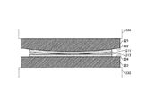
また、本実施例において「貼り合わせ」とは、本実施例に記載の方法で積層された二つの基板に設けられた端子が互いに接続され、これにより、二つの基板間に電気的な導通が確保された場合もしくは二つの基板の接合強度が所定の強度以上となる場合には、それらの状態を指す。また、本実施例に記載の方法で積層された二つの基板をその後にアニール等の処理を行うことにより、二つの基板が最終的に電気的に接続される場合もしくは二つの基板の接合強度が所定の強度以上となる場合は、「貼り合わせ」は、アニール等の処理前に二つの基板が一時的に結合している状態、すなわち仮接合されている状態を指す。
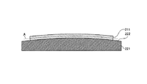
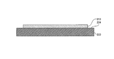
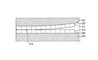
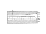
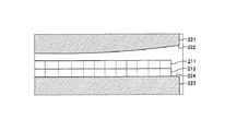
また、本実施例では、基板211、213間に閾値以上の位置ずれが生じる前に、接触領域の拡大を開始させる例を示したが、これに代えて、基板211、213の少なくとも一方に閾値以上の変形が生じる前に接触領域の拡大を開始してもよい。この場合、一方の基板のみが変形する場合は、基板211、213の一部同士が接触する前の状態もしくは基板211、213が位置合わせされた状態を基準として、その一方の基板に生じる変形量の大きさが、基板211、213の接続部間に適切な電気的接続や接合強度が得られないずれを発生する大きさにならないように、閾値が設定される。一方、基板211、213の両方が変形する場合は、変形量の差が、基板211、213の接続部間に適切な電気的接続や接合強度が得られないずれを発生する大きさにならないように、閾値が設定される。
Claims (21)
- 第1の基板における表面の一部と第2の基板における表面の一部とを、前記第1の基板および前記第2の基板の間に温度差を設けて相対位置を補正した状態で接触させて前記一部に接触領域を形成した後に、前記接触領域を拡大させて、前記第1の基板および前記第2の基板を貼り合わせる基板貼り合わせ装置であって、
前記第1の基板および前記第2の基板の間の位置ずれが閾値を超える前に前記接触領域の拡大を開始させ、
前記閾値は、前記第1の基板および前記第2の基板を貼り合わせた後に前記第1の基板および前記第2の基板の間に電気的な導通が可能となるずれ量である基板貼り合わせ装置。 - 前記位置ずれは、前記第1の基板および前記第2の基板の少なくとも一方の歪みにより生じるずれを含む、請求項1に記載の基板貼り合せ装置。
- 前記第1の基板および前記第2の基板のそれぞれの前記表面のまだ接触していない非接触領域の温度差が前記位置ずれの閾値に対応する所定の範囲外になる前に、前記接触領域の拡大を開始する請求項1または2に記載の基板貼り合わせ装置。
- 前記一部に形成された前記接触領域において、前記第1の基板および前記第2の基板の面方向の相対位置が固定される結合力で前記第1の基板および前記第2の基板が互いに結合された後、前記接触領域の拡大を開始する請求項1から3のいずれか一項に記載の基板貼り合わせ装置。
- 前記結合力で結合された前記接触領域が前記一部に形成されたか否かを判断する判断部を備え、前記判断部による判断結果に基づいて、前記接触領域の拡大が開始される請求項4に記載の基板貼り合わせ装置。
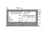
- 前記第1の基板を保持する保持部を備え、
前記保持部による前記第1の基板の保持を解除することにより前記接触領域が拡大され、
前記保持部は、前記第1の基板および前記第2の基板の間に閾値以上の位置ずれが生じる前に、前記第1の基板の保持を解除する請求項1から5のいずれか一項に記載の基板貼り合わせ装置。 - 前記閾値は、前記第1の基板および前記第2の基板にそれぞれ設けられた接続部同士が少なくとも一部で接触するときの前記第1の基板および前記第2の基板の間の位置ずれ量に対応する値である請求項6に記載の基板貼り合わせ装置。
- 前記位置ずれは、前記第1の基板および前記第2の基板の少なくとも一方の温調により前記第1の基板および前記第2の基板の相対位置が補正された状態に対するずれである請求項1から7のいずれか一項に記載の基板貼り合わせ装置。
- 前記補正の補正量を算出する算出部を備え、
前記算出部は、前記接触領域が拡大する過程で前記第1の基板および前記第2の基板の少なくとも一方に生じる歪みによる位置ずれに基づいて、前記補正量を算出する請求項8に記載の基板貼り合わせ装置。 - 前記第1の基板および前記第2の基板の少なくとも一方と外部との熱の交流を制御する温度調節部をさらに備える請求項1から9のいずれか一項に記載の基板貼り合わせ装置。
- 第1の基板における表面の一部と第2の基板における表面の一部とを、前記第1の基板および前記第2の基板の間に温度差を設けて相対位置を補正した状態で接触させて前記一部に接触領域を形成した後に、前記接触領域を拡大させて、前記第1の基板および前記第2の基板を貼り合わせる基板貼り合わせ方法であって、
前記第1の基板および前記第2の基板の間の位置ずれが閾値を超える前に前記接触領域の拡大を開始させる段階を含み、
前記閾値は、前記第1の基板および前記第2の基板を貼り合わせた後に前記第1の基板および前記第2の基板の間に電気的な導通が可能となるずれ量である基板貼り合わせ方法。 - 前記位置ずれは、前記第1の基板および前記第2の基板の少なくとも一方の歪みにより生じるずれを含む、請求項11に記載の基板貼り合わせ方法。
- 前記第1の基板および前記第2の基板のそれぞれの前記表面のまだ接触していない非接触領域の温度差が前記位置ずれの閾値に対応する所定の範囲外になる前に、前記接触領域の拡大を開始する請求項11または12に記載の基板貼り合わせ方法。
- 前記一部に形成された前記接触領域において、前記第1の基板および前記第2の基板の面方向の相対位置が固定される結合力で前記第1の基板および前記第2の基板が互いに結合された後、前記接触領域の拡大を開始する開始段階を有する請求項11から13のいずれか一項に記載の基板貼り合わせ方法。
- 前記結合力で結合された前記接触領域が前記一部に形成されたか否かを判断する判断段階を含み、前記開始段階は、前記判断段階での判断結果に基づいて、前記接触領域の拡大を開始する請求項14に記載の基板貼り合わせ方法。
- 前記第1の基板を保持部に保持する保持段階を含み、
前記開始段階は、前記第1の基板および前記第2の基板の間に閾値以上の位置ずれが生じる前に、前記保持部による前記第1の基板の保持を解除する請求項14または15に記載の基板貼り合わせ方法。 - 前記保持段階では、前記第1の基板および前記第2の基板の歪み量の差による位置ずれを補正する場合に、補正量が小さい方の基板を前記保持部に保持する請求項16に記載の基板貼り合わせ方法。
- 前記閾値は、前記第1の基板および前記第2の基板にそれぞれ設けられた接続部同士が少なくとも一部で接触するときの前記第1の基板および前記第2の基板の間の位置ずれ量に対応する値である請求項16に記載の基板貼り合わせ方法。
- 前記位置ずれは、前記第1の基板および前記第2の基板の少なくとも一方の温調により前記第1の基板および前記第2の基板の相対位置が補正された状態に対するずれである請求項11から18のいずれか一項に記載の基板貼り合わせ方法。
- 前記補正の補正量を算出する算出段階を備え、
前記算出段階は、前記接触領域が拡大する過程で前記第1の基板および前記第2の基板の少なくとも一方に生じる歪みによる位置ずれに基づいて、前記補正量を算出する請求項19に記載の基板貼り合わせ方法。 - 前記第1の基板および前記第2の基板の少なくとも一方と外部との熱の交流を制御する段階をさらに備える請求項11から20のいずれか一項に記載の基板貼り合わせ方法。
Applications Claiming Priority (1)
| Application Number | Priority Date | Filing Date | Title |
|---|---|---|---|
| PCT/JP2016/059985 WO2017168531A1 (ja) | 2016-03-28 | 2016-03-28 | 基板貼り合わせ装置および基板貼り合わせ方法 |
Publications (2)
| Publication Number | Publication Date |
|---|---|
| JPWO2017168531A1 JPWO2017168531A1 (ja) | 2018-12-13 |
| JP6569802B2 true JP6569802B2 (ja) | 2019-09-04 |
Family
ID=59962738
Family Applications (1)
| Application Number | Title | Priority Date | Filing Date |
|---|---|---|---|
| JP2018507853A Expired - Fee Related JP6569802B2 (ja) | 2016-03-28 | 2016-03-28 | 基板貼り合わせ装置および基板貼り合わせ方法 |
Country Status (4)
| Country | Link |
|---|---|
| US (1) | US20190027462A1 (ja) |
| JP (1) | JP6569802B2 (ja) |
| TW (1) | TW201801136A (ja) |
| WO (1) | WO2017168531A1 (ja) |
Families Citing this family (7)
| Publication number | Priority date | Publication date | Assignee | Title |
|---|---|---|---|---|
| CN110959218B (zh) * | 2017-07-18 | 2023-05-16 | 株式会社村田制作所 | 电极压接装置 |
| TWI823598B (zh) * | 2018-01-23 | 2023-11-21 | 日商東京威力科創股份有限公司 | 接合系統及接合方法 |
| WO2020022015A1 (ja) * | 2018-07-25 | 2020-01-30 | 株式会社ニコン | 接合方法および接合装置 |
| AT525844A1 (de) * | 2019-05-13 | 2023-07-15 | Suss Microtec Lithography Gmbh | Bondvorrichtung sowie Verfahren zum Bonden von Substraten |
| JP7357288B2 (ja) | 2020-03-06 | 2023-10-06 | 本田技研工業株式会社 | 半導体装置の製造方法 |
| CN112967965B (zh) * | 2021-03-12 | 2023-11-07 | 长江存储科技有限责任公司 | 对准方法、对准装置、对准设备及计算机存储介质 |
| CN115755769B (zh) * | 2022-12-23 | 2023-06-30 | 深圳市小铭工业互联网有限公司 | 提高pcba制造aoi良率的方法 |
Family Cites Families (12)
| Publication number | Priority date | Publication date | Assignee | Title |
|---|---|---|---|---|
| JP3328878B2 (ja) * | 1998-10-26 | 2002-09-30 | 澁谷工業株式会社 | ボンディング装置 |
| JP3790995B2 (ja) * | 2004-01-22 | 2006-06-28 | 有限会社ボンドテック | 接合方法及びこの方法により作成されるデバイス並びに接合装置 |
| WO2006116030A2 (en) * | 2005-04-21 | 2006-11-02 | Aonex Technologies, Inc. | Bonded intermediate substrate and method of making same |
| US7947570B2 (en) * | 2008-01-16 | 2011-05-24 | Semiconductor Energy Laboratory Co., Ltd. | Manufacturing method and manufacturing apparatus of semiconductor substrate |
| US8267143B2 (en) * | 2009-04-16 | 2012-09-18 | Suss Microtec Lithography, Gmbh | Apparatus for mechanically debonding temporary bonded semiconductor wafers |
| JP4801769B2 (ja) * | 2009-11-30 | 2011-10-26 | 三菱重工業株式会社 | 接合方法、接合装置制御装置、接合装置 |
| JP2013008921A (ja) * | 2011-06-27 | 2013-01-10 | Toshiba Corp | 半導体製造装置及び製造方法 |
| JP5935542B2 (ja) * | 2012-06-28 | 2016-06-15 | 株式会社ニコン | 基板貼り合わせ装置および基板貼り合わせ方法 |
| WO2014064944A1 (ja) * | 2012-10-26 | 2014-05-01 | 株式会社ニコン | 基板貼り合わせ装置、位置合わせ装置、基板貼り合わせ方法、位置合わせ方法、及び、積層半導体装置の製造方法 |
| US9650723B1 (en) * | 2013-04-11 | 2017-05-16 | Soraa, Inc. | Large area seed crystal for ammonothermal crystal growth and method of making |
| JP6317933B2 (ja) * | 2014-01-30 | 2018-04-25 | 芝浦メカトロニクス株式会社 | 貼合基板製造装置及び貼合基板製造方法 |
| JP2015149339A (ja) * | 2014-02-05 | 2015-08-20 | 株式会社東芝 | 半導体装置の製造方法および半導体装置の製造装置 |
-
2016
- 2016-03-28 WO PCT/JP2016/059985 patent/WO2017168531A1/ja active Application Filing
- 2016-03-28 JP JP2018507853A patent/JP6569802B2/ja not_active Expired - Fee Related
-
2017
- 2017-03-24 TW TW106109907A patent/TW201801136A/zh unknown
-
2018
- 2018-09-26 US US16/142,968 patent/US20190027462A1/en not_active Abandoned
Also Published As
| Publication number | Publication date |
|---|---|
| WO2017168531A1 (ja) | 2017-10-05 |
| TW201801136A (zh) | 2018-01-01 |
| US20190027462A1 (en) | 2019-01-24 |
| JPWO2017168531A1 (ja) | 2018-12-13 |
Similar Documents
| Publication | Publication Date | Title |
|---|---|---|
| JP6579262B2 (ja) | 基板貼り合わせ装置および基板貼り合わせ方法 | |
| JP6569802B2 (ja) | 基板貼り合わせ装置および基板貼り合わせ方法 | |
| JP6952853B2 (ja) | 接合システム、および接合方法 | |
| JP6617718B2 (ja) | 基板重ね合わせ装置および基板処理方法 | |
| JP7420185B2 (ja) | 基板貼り合わせ装置および基板貼り合わせ方法 | |
| JP7416119B2 (ja) | 積層基板製造方法、積層基板製造装置、積層基板製造システム、および基板処理装置 | |
| WO2018221391A1 (ja) | 基板貼り合わせ方法、積層基板製造装置及び積層基板製造システム | |
| JP2019129286A (ja) | 積層装置、活性化装置、制御装置、積層体の製造装置、および積層体の製造方法 | |
| JP2018190817A (ja) | 接合装置および接合方法 | |
| JP7234494B2 (ja) | 接合装置および接合方法 | |
| JP7494875B2 (ja) | 基板重ね合わせ装置および基板処理方法 | |
| WO2020179716A1 (ja) | 積層体形成装置および積層体形成方法 | |
| KR20240017966A (ko) | 적층 기판의 제조 방법 및 제조 장치 | |
| JP7105956B2 (ja) | 接合装置 | |
| TWI834891B (zh) | 基板重合方法 |
Legal Events
| Date | Code | Title | Description |
|---|---|---|---|
| A521 | Request for written amendment filed |
Free format text: JAPANESE INTERMEDIATE CODE: A523 Effective date: 20180625 |
|
| A621 | Written request for application examination |
Free format text: JAPANESE INTERMEDIATE CODE: A621 Effective date: 20180820 |
|
| A131 | Notification of reasons for refusal |
Free format text: JAPANESE INTERMEDIATE CODE: A131 Effective date: 20190521 |
|
| A521 | Request for written amendment filed |
Free format text: JAPANESE INTERMEDIATE CODE: A523 Effective date: 20190618 |
|
| TRDD | Decision of grant or rejection written | ||
| A01 | Written decision to grant a patent or to grant a registration (utility model) |
Free format text: JAPANESE INTERMEDIATE CODE: A01 Effective date: 20190709 |
|
| A61 | First payment of annual fees (during grant procedure) |
Free format text: JAPANESE INTERMEDIATE CODE: A61 Effective date: 20190722 |
|
| R150 | Certificate of patent or registration of utility model |
Ref document number: 6569802 Country of ref document: JP Free format text: JAPANESE INTERMEDIATE CODE: R150 |
|
| LAPS | Cancellation because of no payment of annual fees |