JP6435901B2 - Touch panel sensor, touch panel device, and conductive pattern substrate - Google Patents
Touch panel sensor, touch panel device, and conductive pattern substrate Download PDFInfo
- Publication number
- JP6435901B2 JP6435901B2 JP2015024365A JP2015024365A JP6435901B2 JP 6435901 B2 JP6435901 B2 JP 6435901B2 JP 2015024365 A JP2015024365 A JP 2015024365A JP 2015024365 A JP2015024365 A JP 2015024365A JP 6435901 B2 JP6435901 B2 JP 6435901B2
- Authority
- JP
- Japan
- Prior art keywords
- dummy
- touch panel
- electrode
- panel sensor
- constituting
- Prior art date
- Legal status (The legal status is an assumption and is not a legal conclusion. Google has not performed a legal analysis and makes no representation as to the accuracy of the status listed.)
- Active
Links
Images


Description
本発明は、タッチパネルセンサに関する。また本発明は、タッチパネルセンサと保護カバーとを組み合わせることによって得られるタッチパネル装置に関する。また本発明は、導電性を有するパターンを備えた導電性パターン基板に関する。 The present invention relates to a touch panel sensor. The present invention also relates to a touch panel device obtained by combining a touch panel sensor and a protective cover. Moreover, this invention relates to the electroconductive pattern board | substrate provided with the pattern which has electroconductivity.
今日、入力手段として、タッチパネル装置が広く用いられている。タッチパネル装置は一般に、タッチパネルセンサ、保護カバー、タッチパネルセンサ上への接触位置を検出する制御回路、配線およびFPC(フレキシブルプリント基板)などを含んでいる。タッチパネル装置は、多くの場合、液晶ディスプレイや有機ELディスプレイ等の表示装置が組み込まれた種々の装置等(例えば、券売機、ATM装置、携帯電話、ゲーム機)に対する入力手段として、表示装置とともに用いられている。このような装置においては、タッチパネルセンサが表示装置の表示面上に配置されており、これによって、表示装置に対する極めて直接的な入力が可能になっている。タッチパネルセンサのうち表示装置の表示領域に対面する領域は透明になっており、タッチパネルセンサのこの領域が、接触位置(接近位置)を検出し得るアクティブエリアを構成するようになる。 Today, touch panel devices are widely used as input means. The touch panel device generally includes a touch panel sensor, a protective cover, a control circuit for detecting a contact position on the touch panel sensor, wiring, an FPC (flexible printed circuit board), and the like. In many cases, the touch panel device is used together with the display device as an input means for various devices including a display device such as a liquid crystal display or an organic EL display (for example, a ticket vending machine, an ATM device, a mobile phone, a game machine) It has been. In such a device, the touch panel sensor is disposed on the display surface of the display device, thereby enabling extremely direct input to the display device. The area | region which faces the display area of a display apparatus among touch panel sensors is transparent, and this area | region of a touch panel sensor comprises the active area which can detect a contact position (approach position).
タッチパネルセンサとして、投影型容量結合方式のタッチパネルセンサが知られている。容量結合方式のタッチパネルセンサにおいては、位置を検知されるべき外部導体(典型的には、指)が誘電体を介してタッチパネルセンサに接触(接近)する際、新たに奇生容量が発生する。この奇生容量に起因する静電容量の変化に基づいて、タッチパネルセンサ上における外部導体の位置が検出される。このような投影型容量結合方式のタッチパネルセンサは例えば、PETなどからなる基材と、基材の観察者側の面に設けられた複数の第1電極と、基材の表示装置側の面に設けられた複数の第2電極と、を備えている。第1電極および第2電極は、例えば、透光性および導電性を有する透明導電材料から構成される。 As a touch panel sensor, a projection capacitive coupling type touch panel sensor is known. In the capacitive coupling type touch panel sensor, when an external conductor (typically, a finger) whose position is to be detected contacts (approaches) the touch panel sensor via a dielectric, a strange capacitance is newly generated. The position of the external conductor on the touch panel sensor is detected on the basis of the change in capacitance caused by this strange capacitance. Such a projected capacitive coupling type touch panel sensor includes, for example, a base material made of PET or the like, a plurality of first electrodes provided on the surface of the base material on the viewer side, and a surface of the base material on the display device side. A plurality of second electrodes provided. The first electrode and the second electrode are made of a transparent conductive material having translucency and conductivity, for example.
また第1電極および第2電極の電気抵抗値を低くするため、第1電極および第2電極を構成する材料として、透明導電材料よりも高い導電性を有する銀や銅などの金属材料を用いることが提案されている。第1電極および第2電極が金属材料から構成される場合、第1電極および第2電極には、表示装置からの映像光を適切な比率で透過させるための開口部が形成されている。例えば第1電極および第2電極は、金属材料からなり、網目状に配置された導線によって構成されている。 In addition, in order to reduce the electrical resistance values of the first electrode and the second electrode, a metal material such as silver or copper having higher conductivity than the transparent conductive material is used as a material constituting the first electrode and the second electrode. Has been proposed. When the first electrode and the second electrode are made of a metal material, the first electrode and the second electrode are formed with openings for transmitting image light from the display device at an appropriate ratio. For example, the first electrode and the second electrode are made of a metal material and are constituted by conductive wires arranged in a mesh shape.
ところで、第1電極および第2電極が金属材料からなる導線によって構成される場合、金属材料が不透明であることに起因して第1電極および第2電極のパターンが観察者(ユーザー)に視認されてしまうことが考えられる。パターンが視認されることは、金属材料からなる導線がアクティブエリアに不均一に配置されている場合に特に生じやすくなる。このような課題を考慮し、例えば隣接する第1電極の間の領域に、第1電極を構成している導線と同一または同様の導線をダミーパターンとして網目状に配置し、これによって、導線の分布密度を均一化することが考えられる(例えば、特許文献1参照)。この場合、第1電極の領域とその他の領域との区別がつきにくくなり、このため、第1電極のパターンが視認されてしまうことを抑制することができる。このようなダミーパターンは、第1電極間の寄生容量を低下させるという効果をもたらすこともできる。隣接する第2電極の間の領域にも同様のダミーパターンが設けられてもよい。 By the way, when the first electrode and the second electrode are configured by conducting wires made of a metal material, the pattern of the first electrode and the second electrode is visually recognized by an observer (user) because the metal material is opaque. It can be considered. The visibility of the pattern is particularly likely to occur when conductive wires made of a metal material are unevenly arranged in the active area. Considering such a problem, for example, in the region between adjacent first electrodes, conductive wires that are the same as or similar to the conductive wires constituting the first electrodes are arranged in a mesh pattern as a dummy pattern. It is conceivable to make the distribution density uniform (for example, see Patent Document 1). In this case, it becomes difficult to distinguish between the region of the first electrode and the other region, and therefore, it is possible to suppress the first electrode pattern from being visually recognized. Such a dummy pattern can also bring about an effect of reducing the parasitic capacitance between the first electrodes. A similar dummy pattern may be provided in a region between adjacent second electrodes.
電極を構成する導線と、ダミーパターンを構成する導線との間には、両者の導通を防止するよう導線を分断する分断部が多数設けられる。また、ダミーパターンを構成する導線同士の間にも、すなわちダミーパターン内にも分断部が設けられることがある。ところで、分断部が形成された場所において、光は、導線によって遮蔽されることなくタッチパネルセンサを透過することができる。従って、分断部を設けることは、その分だけ光の透過率が局所的に上昇することを導く。一方、電極を構成する導線は、通常は一連のものとして構成されている。すなわち電極内には、分断部が設けられていない。従って、電極が設けられている領域における光の透過率は一般に、分断部を含む、例えばダミーパターンが設けられている領域における光の透過率よりも低くなる。両者の間での透過率の差が大きくなると、電極が観察者に視認されてしまうことになる。 Between the conducting wire constituting the electrode and the conducting wire constituting the dummy pattern, there are provided a number of dividing portions for dividing the conducting wire so as to prevent conduction between the two. Further, a dividing portion may be provided between the conductive wires constituting the dummy pattern, that is, in the dummy pattern. By the way, in the place where the dividing part is formed, the light can pass through the touch panel sensor without being shielded by the conducting wire. Therefore, providing the dividing portion leads to a local increase in the light transmittance. On the other hand, the conducting wire constituting the electrode is usually configured as a series. That is, the dividing part is not provided in the electrode. Therefore, the light transmittance in the region where the electrode is provided is generally lower than the light transmittance in the region including the dividing portion, for example, the region where the dummy pattern is provided. When the difference in transmittance between the two becomes large, the electrode is visually recognized by an observer.
本発明は、このような点を考慮してなされたものであり、電極が設けられている領域における光の透過率と、分断部を含む領域における光の透過率との差が大きくなることを抑制することができるタッチパネルセンサを提供することを目的とする。 The present invention has been made in consideration of such points, and it is noted that the difference between the light transmittance in the region where the electrode is provided and the light transmittance in the region including the dividing portion is increased. It aims at providing the touch panel sensor which can be suppressed.
第1の本発明は、タッチパネルセンサであって、前記タッチパネルセンサの一方の側に設けられ、第1方向に延びる複数の第1電極と、前記タッチパネルセンサの一方の側において前記第1電極の間に設けられた複数の第1ダミー部と、前記タッチパネルセンサの他方の側に設けられ、前記第1方向と交差する第2方向に沿って延びる複数の第2電極と、前記タッチパネルセンサの他方の側において前記第2電極の間に設けられた複数の第2ダミー部と、を備え、前記第1電極および前記第1ダミー部は、遮光性および導電性を有する第1導線を網目状に配置することによって構成されており、前記第2電極および前記第2ダミー部は、遮光性および導電性を有する第2導線を網目状に配置することによって構成されており、前記第1電極を構成する前記第1導線と前記第1ダミー部を構成する前記第1導線との間、または、前記第1ダミー部を構成する前記第1導線同士の間、の少なくともいずれか一方には、隣接する前記第1導線を電気的に絶縁するための複数の第1分断部が設けられており、前記タッチパネルセンサの一方の側から見た場合に、前記複数の第1分断部の少なくとも一部は、前記第2導線と部分的に重なっている、タッチパネルセンサである。 1st this invention is a touch-panel sensor, Comprising: Between the 1st electrode provided in the one side of the said touch-panel sensor, the some 1st electrode extended in a 1st direction, and the said 1st electrode in the one side of the said touch-panel sensor A plurality of first dummy parts provided on the other side of the touch panel sensor, a plurality of second electrodes extending along a second direction intersecting the first direction, and the other side of the touch panel sensor. A plurality of second dummy portions provided between the second electrodes on the side, wherein the first electrode and the first dummy portion have a first conductive wire having light shielding properties and conductivity arranged in a mesh shape The second electrode and the second dummy portion are configured by arranging light-shielding and conductive second conductors in a mesh pattern, and the first electrode is Adjacent to at least one of the first conducting wire and the first conducting wire constituting the first dummy portion, or between the first conducting wires constituting the first dummy portion. A plurality of first dividing portions for electrically insulating the first conducting wire are provided, and when viewed from one side of the touch panel sensor, at least a part of the plurality of first dividing portions is The touch panel sensor partially overlaps the second conductive wire.
第2の本発明は、タッチパネルセンサであって、第1方向に延びる複数の第1電極が設けられた第1の基材と、前記第1の基材において前記第1電極の間に設けられた複数の第1ダミー部と、前記第1の基材と向かい合うよう配置され、前記第1方向と交差する第2方向に沿って延びる複数の第2電極が設けられた第2の基材と、前記第2の基材において前記第2電極の間に設けられた複数の第2ダミー部と、を備え、前記第1電極および前記第1ダミー部は、遮光性および導電性を有する第1導線を網目状に配置することによって構成されており、前記第2電極および前記第2ダミー部は、遮光性および導電性を有する第2導線を網目状に配置することによって構成されており、前記第1電極を構成する前記第1導線と前記第1ダミー部を構成する前記第1導線との間、または、前記第1ダミー部を構成する前記第1導線同士の間、の少なくともいずれか一方には、隣接する前記第1導線を電気的に絶縁するための複数の第1分断部が設けられており、前記タッチパネルセンサの一方の側から見た場合に、前記複数の第1分断部の少なくとも一部は、前記第2導線と部分的に重なっている、タッチパネルセンサである。 2nd this invention is a touch panel sensor, Comprising: The 1st base material provided with the some 1st electrode extended in a 1st direction, and the said 1st base material, It is provided between the said 1st electrode. A plurality of first dummy portions, and a second base material provided with a plurality of second electrodes arranged to face the first base material and extending along a second direction intersecting the first direction. A plurality of second dummy portions provided between the second electrodes in the second base material, wherein the first electrode and the first dummy portion have a light shielding property and a conductivity. The second electrode and the second dummy portion are configured by arranging a second conductive wire having light shielding properties and conductivity in a mesh shape, and the second electrode and the second dummy portion are configured by arranging the conductive wire in a mesh shape, The first conductive wire and the first dummy part constituting the first electrode In order to electrically insulate the adjacent first conductors between at least one of the first conductors formed or between the first conductors constituting the first dummy portion. A plurality of first dividing portions are provided, and when viewed from one side of the touch panel sensor, at least a part of the plurality of first dividing portions partially overlaps the second conducting wire. It is a touch panel sensor.
本発明によるタッチパネルセンサにおいて、前記第2電極を構成する前記第2導線と前記第2ダミー部を構成する前記第2導線との間、または、前記第2ダミー部を構成する前記第2導線同士の間、の少なくともいずれか一方には、隣接する前記第2導線を電気的に絶縁するための複数の第2分断部が設けられていてもよい。この場合、好ましくは、前記タッチパネルセンサの一方の側から見た場合に、前記複数の第2分断部の少なくとも一部は、前記第1導線と少なくとも部分的に重なっている。 In the touch panel sensor according to the present invention, the second conductors constituting the second electrode and the second conductors constituting the second dummy part, or the second conductors constituting the second dummy part. A plurality of second dividing portions for electrically insulating the adjacent second conducting wires may be provided in at least one of the two. In this case, preferably, when viewed from one side of the touch panel sensor, at least a part of the plurality of second dividing portions at least partially overlaps the first conductor.
本発明によるタッチパネルセンサにおいて、前記第1ダミー部を構成する前記第1導線同士の間には、隣接する前記第1導線を電気的に絶縁するための前記複数の第1分断部が設けられており、前記第2ダミー部を構成する前記第2導線同士の間には、隣接する前記第2導線を電気的に絶縁するための前記複数の第2分断部が設けられていてもよい。この場合、好ましくは、前記第1ダミー部と前記第2ダミー部とが重なる領域には、前記第1分断部が前記第2導線と少なくとも部分的に重なっている部分、および、前記第2分断部が前記第1導線と少なくとも部分的に重なっている部分の両方が存在している。さらに好ましくは、前記第1分断部が前記第2導線と少なくとも部分的に重なっている部分、および、前記第2分断部が前記第1導線と少なくとも部分的に重なっている部分は、所定の方向に沿って交互に並んでいる。 In the touch panel sensor according to the present invention, the plurality of first dividing portions for electrically insulating the adjacent first conductive wires are provided between the first conductive wires constituting the first dummy portion. In addition, a plurality of second dividing portions for electrically insulating the adjacent second conductive wires may be provided between the second conductive wires constituting the second dummy portion. In this case, preferably, in a region where the first dummy portion and the second dummy portion overlap, a portion where the first dividing portion at least partially overlaps the second conductor, and the second dividing portion There are both portions where the portion at least partially overlaps the first conductor. More preferably, the portion where the first divided portion at least partially overlaps the second conductor, and the portion where the second divided portion at least partially overlaps the first conductor are in a predetermined direction. Are lined up alternately.
本発明によるタッチパネルセンサにおいて、前記第1電極は、前記第1方向に沿って並べられた複数の第1膨出部と、隣接する2つの前記第1膨出部を接続する第1ライン部と、を含み、前記第2方向における前記第1膨出部の幅は、前記第2方向における前記第1ライン部の幅よりも大きくなっており、前記第2電極は、前記第2方向に沿って並べられた複数の第2膨出部と、隣接する2つの前記第2膨出部を接続する第2ライン部と、を含み、前記第1方向における前記第2膨出部の幅は、前記第1方向における前記第2ライン部の幅よりも大きくなっており、前記タッチパネルセンサの一方の側から見た場合の、前記第1膨出部と前記第2膨出部との間の間隔が、1mm以下になっていてもよい。 In the touch panel sensor according to the present invention, the first electrode includes a plurality of first bulging portions arranged along the first direction, and a first line portion connecting the two adjacent first bulging portions. The width of the first bulge portion in the second direction is larger than the width of the first line portion in the second direction, and the second electrode extends along the second direction. A plurality of second bulging portions arranged in parallel and a second line portion connecting two adjacent second bulging portions, and the width of the second bulging portion in the first direction is: The distance between the first bulging portion and the second bulging portion, which is larger than the width of the second line portion in the first direction and viewed from one side of the touch panel sensor. However, it may be 1 mm or less.
本発明によるタッチパネルセンサにおいて、前記複数の第1導線は、複数の第1導線が互いに交わることによって形成される複数の交点が不規則に並ぶよう配置されており、前記複数の第2導線は、複数の第2導線が互いに交わることによって形成される複数の交点が不規則に並ぶよう配置されていてもよい。 In the touch panel sensor according to the present invention, the plurality of first conductors are arranged such that a plurality of intersections formed by the plurality of first conductors intersecting each other are irregularly arranged, and the plurality of second conductors are A plurality of intersections formed by a plurality of second conducting wires crossing each other may be arranged irregularly.
第3の本発明は、上記記載のタッチパネルセンサと、タッチパネルセンサの観察者側に配置された保護カバーと、を備えるタッチパネル装置であって、前記保護カバーは、ガラス又は合成樹脂から構成されている、タッチパネル装置である。 3rd this invention is a touchscreen apparatus provided with the touchscreen sensor of the said description, and the protective cover arrange | positioned at the observer side of a touchscreen sensor, Comprising: The said protective cover is comprised from glass or a synthetic resin. The touch panel device.
第4の本発明は、導電性パターン基板であって、前記導電性パターン基板の一方の側に設けられ、第1方向に延びる複数の第1電極と、前記導電性パターン基板の一方の側において前記第1電極の間に設けられた複数の第1ダミー部と、前記導電性パターン基板の他方の側に設けられ、前記第1方向と交差する第2方向に沿って延びる複数の第2電極と、前記導電性パターン基板の他方の側において前記第2電極の間に設けられた複数の第2ダミー部と、を備え、前記第1電極および前記第1ダミー部は、遮光性および導電性を有する第1導線を網目状に配置することによって構成されており、前記第2電極および前記第2ダミー部は、遮光性および導電性を有する第2導線を網目状に配置することによって構成されており、前記第1電極を構成する前記第1導線と前記第1ダミー部を構成する前記第1導線との間、または、前記第1ダミー部を構成する前記第1導線同士の間、の少なくともいずれか一方には、隣接する前記第1導線を電気的に絶縁するための複数の第1分断部が設けられており、前記導電性パターン基板の一方の側から見た場合に、前記複数の第1分断部の少なくとも一部は、前記第2導線と部分的に重なっている、導電性パターン基板である。 4th this invention is an electroconductive pattern board | substrate, Comprising: The 1st electrode provided in one side of the said electroconductive pattern board | substrate and extended in a 1st direction, and the one side of the said electroconductive pattern board | substrate A plurality of first dummy portions provided between the first electrodes, and a plurality of second electrodes provided on the other side of the conductive pattern substrate and extending along a second direction intersecting the first direction And a plurality of second dummy portions provided between the second electrodes on the other side of the conductive pattern substrate, wherein the first electrode and the first dummy portion are light-shielding and conductive. The second electrode and the second dummy part are configured by disposing a second conductive wire having light shielding properties and conductivity in a mesh shape. The first electrode Adjacent to at least one of the first conducting wire and the first conducting wire constituting the first dummy portion, or between the first conducting wires constituting the first dummy portion. A plurality of first dividing portions for electrically insulating the first conducting wire to be at least one of the plurality of first dividing portions when viewed from one side of the conductive pattern substrate. The part is a conductive pattern substrate partially overlapping the second conductive wire.
第5の本発明は、導電性パターン基板であって、第1方向に延びる複数の第1電極が設けられた第1の基材と、前記第1の基材において前記第1電極の間に設けられた複数の第1ダミー部と、前記第1の基材と向かい合うよう配置され、前記第1方向と交差する第2方向に沿って延びる複数の第2電極が設けられた第2の基材と、前記第2の基材において前記第2電極の間に設けられた複数の第2ダミー部と、を備え、前記第1電極および前記第1ダミー部は、遮光性および導電性を有する第1導線を網目状に配置することによって構成されており、前記第2電極および前記第2ダミー部は、遮光性および導電性を有する第2導線を網目状に配置することによって構成されており、前記第1電極を構成する前記第1導線と前記第1ダミー部を構成する前記第1導線との間、または、前記第1ダミー部を構成する前記第1導線同士の間、の少なくともいずれか一方には、隣接する前記第1導線を電気的に絶縁するための複数の第1分断部が設けられており、前記導電性パターン基板の一方の側から見た場合に、前記複数の第1分断部の少なくとも一部は、前記第2導線と部分的に重なっている、導電性パターン基板である。 5th this invention is an electroconductive pattern board | substrate, Comprising: Between the 1st base material provided with the several 1st electrode extended in a 1st direction, and the said 1st base material between the said 1st electrode A second base provided with a plurality of first dummy portions provided and a plurality of second electrodes arranged to face the first base material and extending along a second direction intersecting the first direction; And a plurality of second dummy portions provided between the second electrodes in the second base material, wherein the first electrode and the first dummy portion have light shielding properties and conductivity. The first conductive wire is configured by arranging in a mesh shape, and the second electrode and the second dummy portion are configured by arranging a second conductive wire having light shielding properties and conductivity in a mesh shape. The first conductive wire and the first dummy portion constituting the first electrode In order to electrically insulate the adjacent first conductors between at least one of the first conductors formed or between the first conductors constituting the first dummy portion. A plurality of first divided portions are provided, and when viewed from one side of the conductive pattern substrate, at least a part of the plurality of first divided portions partially overlaps the second conductive wire. A conductive pattern substrate.
本発明において、タッチパネルセンサまたは導電性パターン基板の一方の側に設けられる第1電極および第1ダミー部はいずれも、遮光性および導電性を有する第1導線を網目状に配置することによって構成されている。また、タッチパネルセンサまたは導電性パターン基板の他方の側に設けられる第2電極および第2ダミー部はいずれも、遮光性および導電性を有する第2導線を網目状に配置することによって構成されている。また、第1電極を構成する第1導線と第1ダミー部を構成する第1導線との間、または、第1ダミー部を構成する第1導線同士の間、の少なくともいずれか一方には、隣接する第1導線を電気的に絶縁するための複数の第1分断部が設けられている。そして、タッチパネルセンサまたは導電性パターン基板の一方の側から見た場合に、複数の第1分断部の少なくとも一部が、第2導線と少なくとも部分的に重なるよう、第1導線および第2導線が配置されている。この場合、第1分断部が設けられている領域において、光は、少なくとも部分的に第2導線によって遮蔽されることになる。このため、第1分断部を設けることに起因する光の透過率の上昇の程度を小さくすることができる。従って、電極が設けられている領域における光の透過率と、分断部を含む領域における光の透過率との差が大きくなることを抑制することができる。このことにより、電極が観察者に視認されてしまうことを抑制することができる。 In the present invention, each of the first electrode and the first dummy portion provided on one side of the touch panel sensor or the conductive pattern substrate is configured by arranging first conductive wires having light shielding properties and conductivity in a mesh shape. ing. In addition, the second electrode and the second dummy portion provided on the other side of the touch panel sensor or the conductive pattern substrate are both configured by arranging the second conductive wires having light shielding properties and conductivity in a mesh shape. . Further, at least one of the first conductor constituting the first electrode and the first conductor constituting the first dummy part, or between the first conductors constituting the first dummy part, A plurality of first dividing portions for electrically insulating adjacent first conducting wires are provided. And when it sees from one side of a touch panel sensor or a conductive pattern board | substrate, a 1st conducting wire and a 2nd conducting wire are so that at least one part of several 1st part part may overlap with a 2nd conducting wire at least partially. Has been placed. In this case, light is shielded at least partially by the second conductor in the region where the first dividing portion is provided. For this reason, it is possible to reduce the degree of increase in light transmittance caused by providing the first dividing portion. Therefore, it is possible to suppress an increase in the difference between the light transmittance in the region where the electrode is provided and the light transmittance in the region including the dividing portion. This can suppress the electrode from being visually recognized by the observer.
第1の実施の形態
以下、図1乃至図8(a)〜(e)を参照して、本発明の第1の実施の形態の一例について説明する。なお、本明細書に添付する図面においては、図示と理解のしやすさの便宜上、適宜縮尺および縦横の寸法比等を、実物のそれらから変更し誇張してある。
First Embodiment Hereinafter, an example of a first embodiment of the present invention will be described with reference to FIGS. 1 to 8A to 8E. In the drawings attached to the present specification, for the sake of illustration and ease of understanding, the scale, the vertical / horizontal dimension ratio, and the like are appropriately changed and exaggerated from those of the actual ones.
タッチパネル装置およびタッチ位置検出機能付き表示装置
はじめに図1を参照して、タッチ位置検出機能付き表示装置10について説明する。図1に示すように、タッチ位置検出機能付き表示装置10は、液晶ディスプレイや有機ELディスプレイなどの表示装置15と、表示装置15の観察者側に配置されたタッチパネルセンサ30と、タッチパネルセンサ30の観察者側に配置された保護カバー12と、を組み合わせることによって構成されている。表示装置15は、表示面16aを有する表示パネル16と、表示パネル16に接続された表示制御部(図示せず)と、を有している。表示パネル16は、映像を表示することができる矩形状のアクティブエリアA1と、アクティブエリアA1を取り囲むようにしてアクティブエリアA1の外側に配置された非アクティブエリア(額縁領域とも呼ばれる)A2と、を含んでいる。表示制御部は、表示されるべき映像に関する情報を処理し、映像情報に基づいて表示パネル16を駆動する。表示パネル16は、表示制御部の制御信号に基づいて、所定の映像を表示面16aに表示する。すなわち、表示装置15は、文字や図等の情報を映像として出力する出力装置としての役割を担っている。
Touch Panel Device and Display Device with Touch Position Detection Function First, a
タッチパネルセンサ30は、表示装置15の表示面16aに、例えば接着層(図示せず)を介して接着されている。同様に、保護カバー12も、接着層(図示せず)などを介してタッチパネルセンサ30に接着されている。図1において、タッチパネルセンサ30のうち観察者側に位置する面に符号30aが付され、表示装置15側に位置する面に符号30bが付されている。タッチパネルセンサ30および保護カバー12の組み合わせによって、タッチパネル装置20が構成されている。
The
タッチパネルセンサ
次に図2を参照して、タッチパネルセンサ30について説明する。図2は、観察者側から見た場合のタッチパネルセンサ30を示す平面図である。
Touch Panel Sensor Next, the
ここでは、タッチパネルセンサ30が、投影型の静電容量結合方式のタッチパネルセンサとして構成される例について説明する。なお、「容量結合」方式は、タッチパネルの技術分野において「静電容量」方式や「静電容量結合」方式等とも呼ばれており、本件では、これらの「静電容量」方式や「静電容量結合」方式等と同義の用語として取り扱う。典型的な静電容量結合方式のタッチパネルセンサは、透光性を有する導電性のパターンを有しており、外部の導体(典型的には人間の指)がタッチパネルセンサに接近することにより、外部の導体とタッチパネルセンサの導電性のパターンとの間でコンデンサ(静電容量)が形成される。そして、このコンデンサの形成に伴った電気的な状態の変化に基づき、タッチパネルセンサ上において外部導体が接近している位置の位置座標が特定される。なお本実施の形態によるタッチパネルセンサ30において採用されている、後述する技術思想は、自己容量方式または相互容量方式のいずれにも対応可能である。
Here, an example in which the
(第1電極および第2電極)
図2に示すように、タッチパネルセンサ30は、タッチパネルセンサ30の一方の側(観察者側)に設けられ、第1方向D1に延びる複数の第1電極41と、タッチパネルセンサ30の他方の側(表示装置15側)に設けられ、第1方向D1と交差する第2方向D2に沿って延びる複数の第2電極46と、を備えている。なお図2においては図示を省略しているが、タッチパネルセンサ30は、タッチパネルセンサ30の一方の側において第1電極41の間に設けられた複数の第1ダミー部42と、タッチパネルセンサ30の他方の側において第2電極46の間に設けられた複数の第2ダミー部47と、をさらに備えている。本実施の形態において、第1電極41および第1ダミー部42は、基材32の第1面(観察者側の面)32a上に設けられている。また第2電極46および第2ダミー部47は、基材32の第2面(表示装置15側の面)32b上に設けられている。なお図2においては、基材32の第1面32a側に設けられている構成要素が実線で表され、基材32の第2面32b側に設けられている構成要素が点線で表されている。後述するように、第1電極41、第1ダミー部42、第2電極46および第2ダミー部47はいずれも、金属材料を含む導線によって構成されている。
(First electrode and second electrode)
As shown in FIG. 2, the
相互容量方式が採用される場合、第1電極41および第2電極46の一方が駆動電極になり、他方が、駆動電極からの信号電圧が印加される検出電極となる。例えば、タッチパネルセンサ30の観察者側に設けられた第1電極41が検出電極になり、タッチパネルセンサ30の表示装置15側に設けられた第2電極46が駆動電極になる。
When the mutual capacitance method is employed, one of the
第1電極41は、第1方向D1に沿って並べられた複数の第1膨出部41aと、隣接する2つの第1膨出部41aを接続するよう第1方向D1に延びる第1ライン部41bと、を含んでいる。第1膨出部41aとは、第1方向D1と交差する第2方向D2における寸法が、第2方向D2における第1ライン部41bの寸法よりも大きくなっている部分のことである。また第2電極46は、第2方向D2に沿って並べられた複数の第2膨出部46aと、隣接する2つの第2膨出部46aを接続するよう第2方向D2に延びる第2ライン部46bと、を含んでいる。第2膨出部46aとは、第2方向D2と交差する第1方向D1における寸法が、第1方向D1における第2ライン部46bの寸法よりも大きくなっている部分のことである。
The
図2に示すように、タッチパネルセンサ30は、タッチ位置を検出され得る領域に対応する矩形状のアクティブエリアAa1と、アクティブエリアAa1の周辺に位置する矩形枠状の非アクティブエリアAa2と、を含んでいる。アクティブエリアAa1および非アクティブエリアAa2はそれぞれ、表示パネル16のアクティブエリアA1および非アクティブエリアA2に対応して区画されたものである。
As shown in FIG. 2, the
上述の第1電極41、第1ダミー部42、第2電極46および第2ダミー部47は、アクティブエリアAa1内に配置されている。また非アクティブエリアAa2のうち基材32の第1面32a上には、各第1電極41に電気的に接続された複数の第1額縁配線43と、基材32の外縁近傍に配置され、各第1額縁配線43に電気的に接続された複数の第1端子部44と、が設けられている。さらに、非アクティブエリアAa2のうち基材32の第2面32b上には、各第2電極46に電気的に接続された複数の第2額縁配線48と、基材32の外縁近傍に配置され、各第2額縁配線48に電気的に接続された複数の第2端子部49と、が設けられている。
The
信号を適切に伝達することができる限りにおいて、第1額縁配線43および第1端子部44並びに第2額縁配線48および第2端子部49の具体的な構成が特に限られることはない。例えば第1額縁配線43および第1端子部44は、第1電極41や第1ダミー部42を構成する後述する第1導線51と同一の層構成で第1導線51と同時に形成されるものであってもよい。同様に、第2額縁配線48および第2端子部49は、第2電極46や第2ダミー部47を構成する後述する第2導線56と同一の層構成で第2導線56と同時に形成されるものであってもよい。
As long as signals can be appropriately transmitted, the specific configurations of the
(基材)
基材32を構成する材料としては、例えば、ポリエチレンテレフタレート(PET)、シクロオレフィンポリマー(COP)やガラスなど、十分な透光性を有する材料が用いられる。基材32が例えばPETを含む場合、PETの厚みは例えば100〜200μmの範囲内になっている。なお電極41,46やダミー部42,47を適切に保持することができる限りにおいて、基材32の具体的な構成が特に限られることはない。例えば、PET層などの表面に設けられたハードコート層がさらに基材32に含まれていてもよい。すなわち本実施の形態において、基材32とは、何らかの具体的な構造や材料を意味するものではなく、タッチパネルセンサ30を構成する第1電極41や第2電極46などのパターンの下地となるものを意味するに過ぎない。
(Base material)
As a material constituting the
(保護カバー)
保護カバー12は、表示装置15やタッチパネルセンサ30を保護するためのものである。保護カバー12を構成する材料としては、ガラスを用いてもよく、若しくは、アクリル樹脂、ポリカーボネート樹脂、ポリエチレンテレフタレート樹脂などの合成樹脂やそれらの積層体を用いてもよい。ガラスは、合成樹脂に比べて高い比誘電率を有しており、このため、合成樹脂が用いられる場合に比べてタッチパネル装置20の検出感度を高くすることができる。一方、合成樹脂は、ガラスに比べて低い温度で成形され得る。このため、合成樹脂を用いて保護カバー12を作製することにより、様々な形状を容易に保護カバー12に持たせることができる。例えば図1に示すように、合成樹脂によって構成された保護カバー12に湾曲面13aを設けることが容易に可能になる。
(Protective cover)
The
(第1電極および第1ダミー部の詳細について)
次に図3Aおよび図3Bを参照して、第1電極41および第1ダミー部42について説明する。図3Aは、タッチパネルセンサ30の一方の側から見た場合の第1電極41および第1ダミー部42を拡大して示す平面図であり、図3Bは、図3Aにおいて符号IIIBが付された二点鎖線で囲まれた部分における第1電極41および第1ダミー部42をさらに拡大して示す平面図である。
(Details of first electrode and first dummy part)
Next, the
第1電極41および第1ダミー部42は、遮光性および導電性を有する第1導線51を、各第1導線51の間に開口部52が形成されるよう網目状に配置することによって構成されている。第1導線51は、後述するように、金属材料からなる第1金属層61を含んでいる。第1導線51に含まれる金属材料としては、例えば、銀、銅、アルミニウムまたはこれらの合金等を挙げることができる。
The
第1電極41や第1ダミー部42が広がる領域の面積のうち開口部52によって占められる面積の比率(以下、開口率と称する)が十分に高くなり、これによって、表示装置15からの映像光が適切な透過率でタッチパネルセンサ30のアクティブエリアAa1を透過することができる限りにおいて、第1導線51の寸法や形状が特に限られることはない。例えば第1電極41および第1ダミー部42は、開口部52の形状が菱形の形状になるように複数の第1導線51を配置することによって構成されている。本実施の形態においては、菱形の内角のうち鋭角になる内角が第1方向D1に沿って並ぶよう、第1導線51が構成されている。開口率の範囲は、表示装置から放出される映像光の特性などに応じて適宜設定される。
The ratio of the area occupied by the opening 52 (hereinafter referred to as the opening ratio) out of the area of the region where the
第1導線51の線幅は、求められる開口率などに応じて設定されるが、例えば第1導線51の幅は1〜10μmの範囲内、より好ましくは2〜7μmの範囲内に設定されている。これによって、観察者が視認する映像に対して第1導線51が及ぼす影響を、無視可能な程度まで低くすることができる。第1導線51の厚みは、第1電極41に対して求められる電気抵抗値などに応じて適宜設定されるが、例えば0.1〜0.5μmの範囲内となっている。
The line width of the
図3Aおよび図3Bに示すように、第1電極41を構成する第1導線51と第1ダミー部42を構成する第1導線51との間には、複数の第1分断部53が設けられている。このような第1分断部53を設けることにより、第1電極41と第1ダミー部42との間を電気的に絶縁することができる。通常は、1つの第1分断部53を挟んで隣接する2つの第1導線51の一方を延長すると他方の第1導線51に重なるよう、第1分断部53および第1導線51が構成されている。第1導線51が延びる方向における第1分断部53の寸法は、例えば1〜500μmの範囲内に設定される。
As shown in FIGS. 3A and 3B, a plurality of
第1電極41と第1ダミー部42との間の境界部の形状、すなわち第1電極41の輪郭は、第1電極41と第1ダミー部42との間の第1分断部53の配置によって画定される。図3Aおよび図3Bにおいて、タッチパネルセンサ30の一方の側からタッチパネルセンサ30を見た場合における、すなわち平面視における第1電極41の輪郭が、符号B1が付された一点鎖線によって示されている。
The shape of the boundary portion between the
また図3Bに示すように、第1ダミー部42を構成する第1導線51同士の間にも、複数の第1分断部53が設けられていてもよい。なお図3Aにおいては、第1ダミー部42内の第1分断部53が便宜上省略されている。
Further, as shown in FIG. 3B, a plurality of
(第2電極および第2ダミー部の詳細について)
次に図4Aおよび図4Bを参照して、第2電極46および第2ダミー部47について説明する。図4Aは、タッチパネルセンサ30の一方の側から見た場合の第2電極46および第2ダミー部47を拡大して示す平面図であり、図4Bは、図4Aにおいて符号IVBが付された二点鎖線で囲まれた部分における第2電極46および第2ダミー部47をさらに拡大して示す平面図である。
(Details of second electrode and second dummy part)
Next, the
第1電極41および第1ダミー部42の場合と同様に、第2電極46および第2ダミー部47は、遮光性および導電性を有する第2導線56を、各第2導線56の間に開口部57が形成されるよう網目状に配置することによって構成されている。第2導線56は、後述するように、金属材料からなる第2金属層66を含んでいる。第2導線56に含まれる金属材料としては、第1導線51の場合と同様に、例えば、銀、銅、アルミニウムまたはこれらの合金等を挙げることができる。
As in the case of the
第1導線51の場合と同様に、第2導線56の寸法や形状が特に限られることはない。ここでは、第2電極46および第2ダミー部47が、開口部57の形状が菱形の形状になるように複数の第2導線56を配置することによって構成される例が示されている。具体的には、菱形の内角のうち鈍角になる内角が第2方向D2に沿って並ぶよう、第2導線56が構成されている。
As in the case of the
第2導線56の線幅や厚みは、第1導線51と同等に設定されてもよく、若しくは、第1導線51とは異なるように設定されてもよい。
The line width and thickness of the
図4Aおよび図4Bに示すように、第2電極46を構成する第2導線56と第2ダミー部47を構成する第2導線56との間には、複数の第2分断部58が設けられている。このような第2分断部58を設けることにより、第2電極46と第2ダミー部47との間を電気的に絶縁することができる。通常は、1つの第2分断部58を挟んで隣接する2つの第2導線56の一方を延長すると他方の第2導線56に重なるよう、第2分断部58および第2導線56が構成されている。第2導線56が延びる方向における第2分断部58の寸法は、例えば1〜500μmの範囲内に設定される。
As shown in FIGS. 4A and 4B, a plurality of
第2電極46と第2ダミー部47との間の境界部の形状、すなわち第2電極46の輪郭は、第2電極46と第2ダミー部47との間の第2分断部58の配置によって画定される。図4Aおよび図4Bにおいて、平面視における第2電極46の輪郭が、符号B2が付された一点鎖線によって示されている。
The shape of the boundary portion between the
また図4Bに示すように、第1ダミー部42を構成する第2導線56同士の間にも、複数の第2分断部58が設けられていてもよい。なお図4Aにおいては、第2ダミー部47内の第2分断部58が便宜上省略されている。
As shown in FIG. 4B, a plurality of
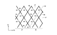
図5Aは、図3Aに示す第1電極41および第1ダミー部42並びに図4Aに示す第2電極46および第2ダミー部47を重ねて示す平面図である。また図5Bは、図5Aにおいて符号VBが付された二点鎖線で囲まれた部分を拡大して示す平面図である。なお図5Aおよび図5Bにおいては、便宜上、タッチパネルセンサ30の一方の側に設けられている、第1電極41や第1ダミー部42などの構成要素が、タッチパネルセンサ30の他方の側に設けられている、第2電極46や第2ダミー部47などの構成要素よりも太い線で表されている。ここでは、図5Aおよび図5Bに示すように、第1導線51同士の交点51aと第2導線56同士の交点56aとが互いに重ならないように第1導線51および第2導線56が配置されている例が示されている。
FIG. 5A is a plan view showing the
ところで、第1分断部53または第2分断部58が形成された場所においては、光は、第1導線51または第2導線56によって遮蔽されることなくタッチパネルセンサ30を透過することができる。従って、第1分断部53や第2分断部58が無秩序に配置される場合、第1分断部53や第2分断部58によって占められる領域の面積の分だけ、分断部53,58を含まない、電極41,46が設けられている領域における光の透過率と、分断部53,58を含む、ダミー部42,47が設けられている領域における光の透過率との差が大きくなってしまう。
By the way, in the place where the
例えば、タッチパネルセンサ30のアクティブエリアAa1を、平面視において第1電極41と第2電極46とが重なる領域(以下、第1領域とも称する)、平面視において第1電極41と第2ダミー部47とが重なる領域または第2電極46と第1ダミー部42とが重なる領域(以下、第2領域とも称する)、および、平面視において第1ダミー部42と第2ダミー部47とが重なる領域(以下、第3領域とも称する)に分類して考える。この場合、第1領域においては、タッチパネルセンサ30の一方の側および他方の側のいずれにも分断部53,58が存在しない。一方、第2領域においては、タッチパネルセンサ30の一方の側および他方の側のいずれか一方に分断部53,58が存在する。また第3領域においては、タッチパネルセンサ30の一方の側および他方の側の両方に分断部53,58が存在する。従って、第1分断部53や第2分断部58の位置が無秩序に設定される場合、第1領域における光の透過率T1、第2領域における光の透過率T2および第3領域における光の透過率T3は、T1<T2<T3という関係を示すようになる。例えば、第1導線51および第2導線56の開口率が95%であり、基材32における光の透過率が100%であると仮定する場合、T1=95%、T2=96%、T3=97%というような透過率の分布になり得る。この場合、第1領域、第2領域および第3領域は、観察者によって比較的に容易に識別され得る。
For example, the active area Aa1 of the
また、保護カバー12を構成する材料として上述のように合成樹脂が用いられる場合、合成樹脂の比誘電率がガラスに比べて低いため、その分だけタッチパネル装置20の検出感度が低下してしまう。このような問題を解決する方法の1つとして、平面視における第1電極41と第2電極46との間の間隔dを大きくすることが考えられる。なぜなら、間隔dを大きくすることにより、第1電極41から第2電極46に至る電気力線の経路がより観察者側にまで広がるようにすることができ、これによって、外部導体の接近や接触をより精度良く検出できるようになるからである。間隔dは、保護カバー12を構成する材料の比誘電率や保護カバー12の厚みに応じて適宜設定されるが、例えば0.1〜1mmの範囲内に設定される。
一方、平面視において第1電極41と第2電極46との間に位置することになる領域は、第1ダミー部42と第2ダミー部47とが重なる上述の第3領域である。従って、間隔dが大きくなることは、アクティブエリアAa1における上述の第3領域の面積の比率がより大きくなることを意味している。このことは、第1領域、すなわち電極41,46が観察者により視認され易くなってしまうことを導く可能性がある。
Further, when a synthetic resin is used as a material constituting the
On the other hand, the region located between the
このような課題を考慮し、本件発明者は、タッチパネルセンサ30の一方の側から見た場合に、各第1分断部53が第2導線56に少なくとも部分的に重なり、各第2分断部58が第1導線51に少なくとも部分的に重なるよう、第1導線51および第1分断部53並びに第2導線56および第2分断部58を配置することを提案する。図6は、タッチパネルセンサ30を図5BのVI線に沿って切断した場合を示す断面図であり、図7は、タッチパネルセンサ30を図5BのVII線に沿って切断した場合を示す断面図である。図6には、基材32の法線方向に沿って一方の側からタッチパネルセンサ30を見た場合に、各第1分断部53が第2導線56に少なくとも部分的に重なっている様子が示されている。図7には、基材32の法線方向に沿って一方の側からタッチパネルセンサ30を見た場合に、各第2分断部58が第1導線51に少なくとも部分的に重なっている様子が示されている。
In view of such a problem, the present inventor, when viewed from one side of the
本実施の形態によれば、第1分断部53が設けられている領域において、光は、少なくとも部分的に第2導線56によって遮蔽されることになる。同様に、第2分断部58が設けられている領域において、光は、少なくとも部分的に第1導線51によって遮蔽されることになる。このため、第1分断部53または第2分断部58が設けられている上述の第2領域や第3領域における光の透過率T2,T3と、第1分断部53および第2分断部58が存在しない上述の第1領域における光の透過率T1との差が大きくなってしまうことを抑制することができる。このことにより、電極41,46が観察者に視認されてしまうことを抑制することができる。また、第3領域における光の透過率T3と第1領域における光の透過率T1との差を小さくすることができるので、比誘電率の低い合成樹脂を含む保護カバー12が用いられる場合に、タッチパネル装置20の検出感度向上という目的を重視して第1電極41と第2電極46との間の間隔dを大きく設定する、という構成を採用することが可能になる。従って、電極41,46が視認されることが抑制され、かつ十分な検出感度が達成されたタッチパネル装置20を提供することができる。
According to the present embodiment, light is shielded at least partially by the
好ましくは、平面視において第1ダミー部42と第2ダミー部47とが重なる上述の第3領域には、第1分断部53が第2導線56と少なくとも部分的に重なっている部分、および、第2分断部58が第1導線51と少なくとも部分的に重なっている部分の両方が存在している。これによって、第1領域における光の透過率T1と第3領域における光の透過率T3との差をより小さくすることができる。
Preferably, in the above-described third region where the
また好ましくは、平面視において第1ダミー部42と第2ダミー部47とが重なる上述の第3領域には、第1分断部53が第2導線56と少なくとも部分的に重なっている部分、および、第2分断部58が第1導線51と少なくとも部分的に重なっている部分が、所定の方向に沿って交互に並ぶようになっている。例えば図5Bにおいては、第3領域において、第1分断部53が第2導線56と少なくとも部分的に重なっている部分、および、第2分断部58が第1導線51と少なくとも部分的に重なっている部分が、第2方向D2に平行な矢印L2で示す方向に沿って交互に並んでいる様子が示されている。このように第1分断部53と第2分断部58とが交互に並ぶようにすることによって、第3領域における透過率の分布をより均一化することができ、これによって、タッチパネルセンサ30の意匠性をより向上させることができる。
Preferably, in the above-described third region where the
タッチパネルセンサの製造方法
次に、以上のような構成からなるタッチパネルセンサ30を製造する方法について、図8(a)〜(e)を参照して説明する。
Method for Manufacturing Touch Panel Sensor Next, a method for manufacturing the
はじめに図8(a)に示すように、タッチパネルセンサ30を作製するための元材としての積層体60(ブランクとも呼ばれる)を準備する。積層体60は、基材32と、基材32の第1面32a上に設けられ、遮光性および導電性を有する第1金属層61と、基材32の第2面32b上に設けられ、遮光性および導電性を有する第2金属層66と、を備えている。基材32の各面32a,32b上に金属層61,66を設ける方法が特に限られることはなく、蒸着法やスパッタリング法などの公知の方法が適宜用いられ得る。
First, as shown in FIG. 8A, a laminate 60 (also referred to as a blank) as a base material for producing the
次に図8(b)に示すように、第1金属層61上に第1感光層71を設け、かつ、第2金属層66上に第2感光層76を設ける。第1感光層71および第2感光層76は、特定波長域の光、例えば紫外線に対する感光性を有している。感光層71,76のタイプが特に限られることはない。例えば光硬化型の感光層が用いられてもよく、若しくは光硬化型の感光層が用いられてもよい。ここでは、光溶解型の感光層が用いられる例について説明する。第1金属層61上および第2金属層66上に第1感光層71および第2感光層76を設ける方法としては、例えば、ドライフィルムレジストを第1金属層61上および第2金属層66上にそれぞれ貼付するという方法や、感光材を第1金属層61上および第2金属層66上にそれぞれ塗布するという方法を採用することができる。
Next, as shown in FIG. 8B, the first
(露光工程)
その後、図8(b)に示すように、所定のパターンで遮光部72aおよび開口部72bが形成された第1露光マスク72を第1感光層71の近傍に設置し、かつ、所定のパターンで遮光部77aおよび開口部77bが形成された第2露光マスク77を第2感光層76の近傍に設置する。第1露光マスク72の遮光部72aのパターンは、開口部52および第1分断部53のパターンに対応しており、第1露光マスク72の開口部72bのパターンは、第1導線51のパターンに対応している。また第2露光マスク77の遮光部77aのパターンは、開口部57および第2分断部58のパターンに対応しており、第2露光マスク77の開口部77bのパターンは、第2導線56のパターンに対応している。次に、第1露光マスク72に対する第2露光マスク77の相対位置を調整する。例えば、第1露光マスク72または第2露光マスク77のいずれか一方の露光マスクに形成されているアライメントマークを基準として、他方の露光マスクの位置を調整する。若しくは、基材32などに設けられている同一のアライメントマークを共通に用いて、第1露光マスク72および第2露光マスク77の位置を調整する。これによって、第1露光マスク72に対して高い位置精度で第2露光マスク77を配置することができる。その後、第1露光マスク72を介して第1感光層71に所定のパターンで露光光を照射し、かつ、第2露光マスク77を介して第2感光層76に所定のパターンで露光光を照射する露光工程を実施する。なお、第1感光層71に対する露光光の照射と、第2感光層76に対する露光光の照射は、同時に実施されてもよく、異なるタイミングで実施されてもよい。
(Exposure process)
After that, as shown in FIG. 8B, a
(現像工程)
次に、第1感光層71および第2感光層76を現像する。これによって、図8(c)に示すように、パターニングされた第1感光層71および第2感光層76を得ることができる。
(Development process)
Next, the first
(エッチング工程)
その後、図8(d)に示すように、第1感光層71をレジストとして第1金属層61をウェットエッチングする。これによって、電極41および第1ダミー部42の第1導線51に対応するパターンで第1金属層61をパターニングすることができる。また、第2感光層76をレジストとして第2金属層66をウェットエッチングする。これによって、第2電極46および第2ダミー部47の第2導線56に対応するパターンで第2金属層66をパターニングすることができる。次に、図8(e)に示すように、感光層71,76を除去する。このようにして、上述のタッチパネルセンサ30を得ることができる。
(Etching process)
Thereafter, as shown in FIG. 8D, the
なお図示はしないが、第1導線51および第2導線56には、第1導線51および第2導線56による光の反射を抑制するための低反射処理が施されていてもよい。例えば第1導線51の表面には、黒化処理が施されていてもよい。また、第2導線56は、金属材料からなる層に加えて、金属材料からなる層と基材32の第2面32bとの間に設けられた低反射層をさらに含んでいてもよい。
Although not illustrated, the
本実施の形態によれば、タッチパネルセンサ30の一方の側から見た場合に、第1分断部53が第2導線56と少なくとも部分的に重なり、かつ第2分断部58が第1導線51と少なくとも部分的に重なるよう、第1導線51および第2導線56が配置されている。このため、分断部53,58を設けることに起因する光の透過率の上昇の程度を小さくすることができる。従って、分断部53,58を含まない領域における光の透過率と、分断部53,58を含む領域における光の透過率との差が大きくなることを抑制することができる。このことにより、電極41,46が観察者に視認されてしまうことを抑制することができる。
According to the present embodiment, when viewed from one side of the
また本実施の形態によれば、露光工程において、第1露光マスク72に対する第2露光マスク77の相対位置が調整される。このため、基材32の第1面32a側に設けられる第1導線51や第1分断部53に対する、基材32の第2面32b側に設けられる第2導線56や第2分断部58の相対的な位置精度を高めることができる。従って、第1分断部53と第2導線56とを精度良く重ねることができ、また、第2分断部58と第1導線51とを精度良く重ねることができる。このことにより、分断部53,58を設けることに起因する光の透過率の上昇の程度をより小さくすることができる。
Further, according to the present embodiment, the relative position of the second exposure mask 77 with respect to the
第2の実施の形態
次に図9および図10を参照して、本発明の第2の実施の形態について説明する。ここでは、ウェットエッチングによって金属層61,66をパターニングして導線51,56を作製する場合に金属層61,66上に形成される感光層71,76を露光するための露光マスク72,77の具体的なパターンの例について説明する。本実施の形態において、図1乃至図8に示す第1の実施の形態と同一部分には同一符号を付して詳細な説明は省略する。また、第1の実施の形態において得られる作用効果が本実施の形態においても得られることが明らかである場合、その説明を省略することもある。
Second Embodiment Next, with reference to FIGS. 9 and 10, a second embodiment of the present invention will be described. Here, when the
図9(a)は、第1感光層71を露光するための第1露光マスク72のパターンの一例を示す平面図である。ここでは、第1導線51の交点51aとなる部分およびその周辺の部分に照射される露光光を生成するための第1露光マスク72のパターンについて具体的に説明する。図9(a)に示すように、第1露光マスク72は、第1導線51に対応するパターンで線状に延びる複数の開口部72bと、線状に延びる開口部72bを画定するように広がる遮光部72aと、を含んでいる。図9(a)において、異なる方向に線状に延びる開口部72bが互いに接続される部分(以下、接続部分とも称する)が符号72kで表され、また線状に延びる開口部72bの交点が符号72cで表されている。図9(a)に示す例において、第1露光マスク72の線状に延びる開口部72bは、交点72cからの距離に依らず同一の幅sを有している。
FIG. 9A is a plan view showing an example of a pattern of the
図9(b)は、図9(a)に示す第1露光マスク72を用いて露光することにより得られた第1感光層71をレジストとして第1金属層61をウェットエッチングすることによって得られる第1導線51のパターンの一例を示す平面図である。図9(b)に示すように、異なる方向に延びる第1導線51が互いに接続される接続部分51kの形状は、第1露光マスク72の対応する接続部分72kの形状とは異なっている。具体的には、第1導線51の接続部分51kは、第1露光マスク72の接続部分72kよりも広がった形状を有している。このことは、第1露光マスク72を用いて第1感光層71を露光する際に、第1感光層71の解像性の限界のため、接続部分72kの形状が完全には第1感光層71に反映されず、第1露光マスク72の接続部分72kに対応する第1感光層71の接続部分の形状が、図9(b)に示す第1導線51の接続部分51kのように鈍った形状になることに起因していると考えられる。また、第1金属層61をウェットエッチングする際に、第1露光マスク72の接続部分72kに対応する第1感光層71の接続部分のところにまでエッチング液が十分に侵入することができないことにも起因していると考えられる。接続部分51kにおける第1金属層61のエッチングが不完全なものであるため、図9(b)に示すように、交点51aの近傍における第1導線51の幅w1が、交点51aから遠い部分における第1導線51の幅w2よりも大きくなってしまう。このことは、交点51a近傍の領域における光の反射率が、交点51aから遠い領域における光の反射率よりも高くなり、この結果、交点51aが視認されやすくなる、ということを導く。すなわち、交点51aからの距離に応じて、光の反射率および透過率が局所的にばらついてしまうことが考えられる。
FIG. 9B is obtained by wet etching the
このような課題を考慮すると、図10(a)に示すようなパターンで第1露光マスク72の接続部分72kが形成されることが好ましいと考えらえる。図10(a)に示す例において、第1露光マスク72の線状に延びる開口部72bのうち、接続部分72kに接しているまたは接続部分72kを含む部分(以下、第1部分とも称する)が符号72xで表されている。また、第1露光マスク72の線状に延びる開口部72bのうち、第1部分72xよりも交点72cから遠位に設けられ、かつ第1部分72xに接続されている部分(以下、第2部分とも称する)が符号72yで表されている。また、第2部分72yを交点72c近傍にまで仮想的に延長した場合の線が点線で表されている。図10(a)に示すように、第1露光マスク72の線状に延びる開口部72bの第1部分72xは、第2部分72yを延長した点線よりも交点72c側に位置するよう設けられている。すなわち、第1露光マスク72の遮光部72aは、図9(a)に示す場合に比べて、交点72cに向かって突出している。この結果、第1露光マスク72の線状に延びる開口部72bの第1部分72xの幅s1は、第2部分72yの幅s2よりも小さくなっている。
Considering such a problem, it can be considered that the
図10(b)は、図10(a)に示す第1露光マスク72を用いて露光することにより得られた第1感光層71をレジストとして第1金属層61をウェットエッチングすることによって得られる第1導線51のパターンの一例を示す平面図である。上述のように、図10(a)に示す例において、第1露光マスク72の線状に延びる開口部72bの第1部分72xは、第2部分72yを延長した点線よりも交点72c側に位置するよう設けられている。このことは、ウェットエッチングの際に、第2部分72yを延長した仮想的な点線が互いに交わる部分に対応して除去された第1感光層71の位置にまでエッチング液が侵入し易くなることを導く。このため図10(b)に示すように、交点51a近傍の領域における第1導線51の幅w1が、交点51aから遠い領域における第1導線51の幅w2よりも大きくなってしまうことを抑制することができる。これによって、交点51a近傍の領域における光の反射率が、交点51aから遠い領域における光の反射率よりも高くなってしまうことを抑制することができる。このことにより、交点51aが視認されることを抑制することができる。
FIG. 10B is obtained by wet etching the
なお、第1露光マスク72の接続部分72kに対応して形成される第1感光層71の接続部分にエッチング液が侵入し易くなるようにすることができる限りにおいて、第1露光マスク72の線状に延びる開口部72bの第1部分72xの具体的な形状が特に限られることはなく、様々な形状が適宜採用され得る。また図示はしないが、第2露光マスク77の線状に延びる開口部77bも、第1露光マスク72の場合と同様の第1部分および第2部分を有していてもよい。
As long as the etching solution can easily enter the connection portion of the first
変形例
上述した実施の形態に対して様々な変更を加えることが可能である。以下、図面を参照しながら、いくつかの変形例について説明する。以下の説明および以下の説明で用いる図面では、上述した実施の形態と同様に構成され得る部分について、上述の各実施の形態における対応する部分に対して用いた符号と同一の符号を用いることとし、重複する説明を省略する。また、上述した実施の形態において得られる作用効果が変形例においても得られることが明らかである場合、その説明を省略することもある。
Modifications Various modifications can be made to the above-described embodiment. Hereinafter, some modifications will be described with reference to the drawings. In the following description and the drawings used in the following description, the same reference numerals as those used for the corresponding parts in each of the above embodiments are used for the parts that can be configured in the same manner as in the above embodiments. The duplicated explanation is omitted. In addition, when it is clear that the operational effects obtained in the above-described embodiment can be obtained in the modified example, the description thereof may be omitted.
(第1の変形例)
上述の実施の形態の形態においては、第1導線51および第2導線56がそれぞれ規則的に配置される例を示した。具体的には、第1導線51の複数の交点51aおよび第2導線56の複数の交点56aがそれぞれ所定の方向に沿って周期的に並ぶよう、第1導線51および第2導線56が配置される例を示した。しかしながら、図11に示すように、第1導線51は、複数の交点51aが不規則に並ぶように配置されていてもよい。図11に示すような第1導線51のパターンは、例えば、はじめに、複数の交点51aがそれぞれ所定の方向に沿って周期的に並ぶように第1導線51を配置し、次に、隣接する交点51a間の距離よりも小さい距離だけ様々な方向で各交点51aをランダムに変位させることにより、作製され得る。複数の交点51aが不規則に並ぶように第1導線51を配置することにより、例えば、モアレを低減するという効果が期待される。なお図示はしないが、第2導線56も、第1導線51の場合と同様に、複数の交点56aが不規則に並ぶように配置されていてもよい。
(First modification)
In the form of the above-described embodiment, an example in which the
図11に示す本変形例においても、第1分断部53が第2導線56と少なくとも部分的に重なり、第2分断部58が第1導線51と少なくとも部分的に重なるよう、第1分断部53の位置および第2分断部58の位置を設定することにより、電極41,46が観察者に視認されてしまうことを抑制することができる。
Also in this modified example shown in FIG. 11, the
(第2の変形例)
また上述の実施の形態の形態においては、第1電極41および第1ダミー部42を構成する第1導線51が、基材32の第1面32a上に設けられ、第2電極46および第2ダミー部47を構成する第2導線56が、基材32の第2面32b上に設けられる例を示した。しかしながら、タッチパネルセンサ30の一方の側から見た場合に、第1分断部53が第2導線56と少なくとも部分的に重なり、第2分断部58が第1導線51と少なくとも部分的に重なることができる限りにおいて、タッチパネルセンサ30の層構成が特に限られることはない。例えば図12Aに示すように、互いに対向する2つの基材32A,32Bの対向面の一方(第1の基材32A)に第1導線51を設け、他方(第2の基材32B)に第2導線56を設け、そして2つの基材32を貼り合わせてもよい。このように2つの基材32A,32Bを貼り合わせる場合であっても、第1導線51によって、タッチパネルセンサ30の一方の側に設けられる第1電極41および第1ダミー部42を構成することができ、また第2導線56によって、タッチパネルセンサ30の他方の側に設けられる第2電極46および第2ダミー部47を構成することができる。また、第1分断部53が第2導線56と少なくとも部分的に重なり、第2分断部58(図示せず)が第1導線51と少なくとも部分的に重なるよう、第1導線51、第1分断部53、第2導線56および第2分断部58を配置することにより、電極41,46が観察者に視認されてしまうことを抑制することができる。
(Second modification)
In the embodiment described above, the first
なお図12Aにおいては、第1の基材32Aのうち第1導線51が設けられている面と、第2の基材32Bのうち第2導線56が設けられている面とが向かい合うように2つの基材32A,32Bを貼りあわせ、これによって、タッチパネルセンサ30の一方の側に設けられる第1導線51の間の第1分断部53が、タッチパネルセンサ30の他方の側に設けられる第2導線56と少なくとも部分的に重なる例を示した。しかしながら、これに限られることはなく、図12Bに示すように、第1の基材32Aのうち第1導線51が設けられている面とは反対側の面と、第2の基材32Bのうち第2導線56が設けられている面とは反対側の面とが向かい合うように、2つの基材32A,32Bを貼りあわせてもよい。その他にも、図12Cに示すように、第1の基材32Aのうち第1導線51が設けられている面とは反対側の面と、第2の基材32Bのうち第2導線56が設けられている面とが向かい合うように、2つの基材32A,32Bを貼りあわせてもよい。これらの場合であっても、第1分断部53が第2導線56と少なくとも部分的に重なり、第2分断部58(図示せず)が第1導線51と少なくとも部分的に重なるよう、第1導線51、第1分断部53、第2導線56および第2分断部58を配置することにより、電極41,46が観察者に視認されてしまうことを抑制することができる。
In FIG. 12A, the surface of the
(第3の変形例)
また上述の実施の形態の形態においては、電極41,46が膨出部41a,46aおよびライン部41b,46bを含む例を示した。すなわち、電極41,46のパターンがいわゆるダイヤモンドパターンである例を示した。しかしながら、電極41,46のパターンが特に限られることはない。例えば図13に示すように、電極41,46のパターンとして、いわゆるストライプパターンが採用されてもよい。この場合であっても、第1分断部53が第2導線56と少なくとも部分的に重なり、第2分断部58が第1導線51と少なくとも部分的に重なるよう、第1導線51、第1分断部53、第2導線56および第2分断部58を配置することにより、電極41,46が観察者に視認されてしまうことを抑制することができる。
(Third Modification)
Moreover, in the form of the above-mentioned embodiment, the
(その他の変形例)
また上述の実施の形態の形態においては、第1分断部53が第2導線56と少なくとも部分的に重なり、かつ第2分断部58が第1導線51と少なくとも部分的に重なる例を示した。しかしながら、これに限られることはなく、第1分断部53は第2導線56と少なくとも部分的に重なっているが、第2分断部58は第1導線51と重なっていなくてもよい。この場合であっても、第1分断部53および第2分断部58が無秩序に配置されている場合に比べれば、電極41,46が設けられている領域における光の透過率と、分断部53,58を含む領域における光の透過率との差を小さくすることができる。
(Other variations)
Further, in the above-described embodiment, the example in which the
また上述の実施の形態の形態においては、複数の第1分断部53の全てが第2導線56に重なっている例を示した。しかしながら、これに限られることはなく、複数の第1分断部53の少なくとも一部が第2導線56に重なっていればよい。例えば、第1電極41と第1ダミー部42との境界を区画する第1分断部53は第2導線56に重なっているが、第1ダミー部42内の第1分断部53は第2導線56に重なっていない、という配置が採用されてもよい。反対に、第1ダミー部42内の第1分断部53は第2導線56に重なっているが、第1電極41と第1ダミー部42との境界を区画する第1分断部53は第2導線56に重なっていない、という配置が採用されてもよい。また、複数の第1分断部53が一定の比率で第2導線56に重なるようになっていてもよい。第2分断部58についても同様に、複数の第2分断部58の少なくとも一部が第1導線51に重なっていればよい。この場合であっても、第1分断部53が無秩序に配置されている場合に比べれば、電極41,46が設けられている領域における光の透過率と、分断部53,58を含む領域における光の透過率との差を小さくすることができる。
Moreover, in the form of the above-mentioned embodiment, the example in which all the some
また上述の実施の形態の形態においては、第1分断部53が第2導線56に少なくとも部分的に重なるように構成された第1電極41、第1ダミー部42、第2電極46および第2ダミー部47を用いて、タッチパネルセンサ30を構成する例を示した。しかしながら、これに限られることはなく、タッチパネルセンサ30以外にも、第1分断部53が第2導線56に少なくとも部分的に重なるように構成された第1電極41、第1ダミー部42、第2電極46および第2ダミー部47を用いて、導電性を有するパターンを備えた導電性パターン基板を構成してもよい。この場合にも、導電性パターン基板において、第1分断部53を設けることに起因する光の透過率の上昇の程度を小さくすることができる。従って、第1電極41が設けられている領域における光の透過率と、第1分断部53を含む領域における光の透過率との差が大きくなることを抑制することができる。このことにより、第1電極41が観察者に視認されてしまうことを抑制することができる。
Further, in the embodiment described above, the
導電性パターン基板の用途は特には限られないが、例えば、導電性パターン基板を用いて移動体用メッシュアンテナや電磁波シールド等を構成することができる。 Although the use of the conductive pattern substrate is not particularly limited, for example, a mesh antenna for a moving body, an electromagnetic wave shield, and the like can be configured using the conductive pattern substrate.
導電性パターン基板においても、タッチパネルセンサ30の場合と同様に、第2分断部58が第1導線51に少なくとも部分的に重なるように第1電極41、第1ダミー部42、第2電極46および第2ダミー部47が構成されていてもよい。またパターン基板においても、タッチパネルセンサ30の場合と同様に、第1電極41および第1ダミー部42を構成する第1導線51と、第2電極46および第2ダミー部47を構成する第2導線56とが、1つの基材の異なる面にそれぞれ設けられていてもよく、若しくは、互いに貼り合わされる2つの基材にそれぞれ設けられていてもよい。
Also in the conductive pattern substrate, as in the case of the
なお、上述した実施の形態に対するいくつかの変形例を説明してきたが、当然に、複数の変形例を適宜組み合わせて適用することも可能である。 In addition, although some modified examples with respect to the above-described embodiment have been described, naturally, a plurality of modified examples can be applied in combination as appropriate.
10 タッチ位置検出機能付き表示装置
12 保護カバー
15 表示装置
20 タッチパネル装置
30 タッチパネルセンサ
32 基材
41 第1電極
41a 第1膨出部
41b 第1ライン部
42 第1ダミー部
46 第2電極
46a 第2膨出部
46b 第2ライン部
47 第2ダミー部
51 第1導線
51a 交点
52 開口部
53 第1分断部
56 第2導線
56a 交点
57 開口部
58 第2分断部
60 積層体
61 第1金属層
66 第2金属層
71 第1感光層
72 第1露光マスク
76 第2感光層
77 第2露光マスク
D1 第1方向
D2 第2方向
DESCRIPTION OF
Claims (8)
前記タッチパネルセンサの一方の側に設けられ、第1方向に延びる複数の第1電極と、
前記タッチパネルセンサの一方の側において前記第1電極の間に設けられた複数の第1ダミー部と、
前記タッチパネルセンサの他方の側に設けられ、前記第1方向と交差する第2方向に沿って延びる複数の第2電極と、
前記タッチパネルセンサの他方の側において前記第2電極の間に設けられた複数の第2ダミー部と、を備え、
前記第1電極および前記第1ダミー部は、遮光性および導電性を有する第1導線を網目状に配置することによって構成されており、
前記第2電極および前記第2ダミー部は、遮光性および導電性を有する第2導線を網目状に配置することによって構成されており、
前記第1電極を構成する前記第1導線と前記第1ダミー部を構成する前記第1導線との間、または、前記第1ダミー部を構成する前記第1導線同士の間、のうち、少なくとも前記第1ダミー部を構成する前記第1導線同士の間には、隣接する前記第1導線を電気的に絶縁するための複数の第1分断部が設けられており、
前記タッチパネルセンサの一方の側から見た場合に、前記第1ダミー部を構成する前記第1導線同士の間の前記複数の第1分断部の少なくとも一部は、前記第2ダミー部を構成する前記第2導線と部分的に重なっている、タッチパネルセンサ。 A touch panel sensor,
A plurality of first electrodes provided on one side of the touch panel sensor and extending in a first direction;
A plurality of first dummy portions provided between the first electrodes on one side of the touch panel sensor;
A plurality of second electrodes provided on the other side of the touch panel sensor and extending along a second direction intersecting the first direction;
A plurality of second dummy portions provided between the second electrodes on the other side of the touch panel sensor,
The first electrode and the first dummy portion are configured by arranging first conductive wires having light shielding properties and conductivity in a mesh shape,
The second electrode and the second dummy portion are configured by arranging second conductive wires having light shielding properties and conductivity in a mesh shape,
Among the first conductors constituting the first electrode and the first conductors constituting the first dummy part, or between the first conductors constituting the first dummy part , at least Between the first conductive wires constituting the first dummy portion, a plurality of first dividing portions for electrically insulating the adjacent first conductive wires are provided,
When viewed from one side of the touch panel sensor, at least a part of the plurality of first dividing portions between the first conductors constituting the first dummy portion constitutes the second dummy portion. A touch panel sensor partially overlapping the second conductive wire.
第1方向に延びる複数の第1電極が設けられた第1の基材と、
前記第1の基材において前記第1電極の間に設けられた複数の第1ダミー部と、
前記第1の基材と向かい合うよう配置され、前記第1方向と交差する第2方向に沿って延びる複数の第2電極が設けられた第2の基材と、
前記第2の基材において前記第2電極の間に設けられた複数の第2ダミー部と、を備え、
前記第1電極および前記第1ダミー部は、遮光性および導電性を有する第1導線を網目状に配置することによって構成されており、
前記第2電極および前記第2ダミー部は、遮光性および導電性を有する第2導線を網目状に配置することによって構成されており、
前記第1電極を構成する前記第1導線と前記第1ダミー部を構成する前記第1導線との間、または、前記第1ダミー部を構成する前記第1導線同士の間、のうち、少なくとも前記第1ダミー部を構成する前記第1導線同士の間には、隣接する前記第1導線を電気的に絶縁するための複数の第1分断部が設けられており、
前記タッチパネルセンサの一方の側から見た場合に、前記第1ダミー部を構成する前記第1導線同士の間の前記複数の第1分断部の少なくとも一部は、前記第2ダミー部を構成する前記第2導線と部分的に重なっている、タッチパネルセンサ。 A touch panel sensor,
A first substrate provided with a plurality of first electrodes extending in a first direction;
A plurality of first dummy portions provided between the first electrodes in the first base material;
A second base material provided with a plurality of second electrodes arranged to face the first base material and extending along a second direction intersecting the first direction;
A plurality of second dummy portions provided between the second electrodes in the second base material,
The first electrode and the first dummy portion are configured by arranging first conductive wires having light shielding properties and conductivity in a mesh shape,
The second electrode and the second dummy portion are configured by arranging second conductive wires having light shielding properties and conductivity in a mesh shape,
Among the first conductors constituting the first electrode and the first conductors constituting the first dummy part, or between the first conductors constituting the first dummy part , at least Between the first conductive wires constituting the first dummy portion, a plurality of first dividing portions for electrically insulating the adjacent first conductive wires are provided,
When viewed from one side of the touch panel sensor, at least a part of the plurality of first dividing portions between the first conductors constituting the first dummy portion constitutes the second dummy portion. A touch panel sensor partially overlapping the second conductive wire.
前記タッチパネルセンサの一方の側から見た場合に、前記第2ダミー部を構成する前記第2導線同士の間の前記複数の第2分断部の少なくとも一部は、前記第1ダミー部を構成する前記第1導線と少なくとも部分的に重なっている、請求項1または2に記載のタッチパネルセンサ。 At least among the second conductor constituting the second electrode and the second conductor constituting the second dummy portion, or between the second conductors constituting the second dummy portion. A plurality of second dividing portions for electrically insulating the adjacent second conductive wires are provided between the second conductive wires constituting the second dummy portion ,
When viewed from one side of the touch panel sensor, at least a part of the plurality of second dividing portions between the second conductors constituting the second dummy portion constitutes the first dummy portion. The touch panel sensor according to claim 1, wherein the touch panel sensor overlaps at least partially with the first conductive wire.
前記複数の第2導線は、複数の第2導線が互いに交わることによって形成される複数の交点が不規則に並ぶよう配置されている、請求項1乃至4のいずれか一項に記載のタッチパネルセンサ。 The plurality of first conductors are arranged such that a plurality of intersections formed by the plurality of first conductors intersecting each other are irregularly arranged,
It said plurality of second conductors, a plurality of intersections where a plurality of second conductor is formed by intersecting each other are arranged so as to align irregular, touch sensor according to any one of claims 1 to 4 .
前記タッチパネルセンサは、請求項1乃至5のいずれか一項のタッチパネルセンサからなり、
前記保護カバーは、合成樹脂から構成されている、タッチパネル装置。 A touch panel device comprising a touch panel sensor and a protective cover disposed on an observer side of the touch panel sensor,
The touch panel sensor comprises the touch panel sensor according to any one of claims 1 to 5 ,
The protective cover is a touch panel device made of synthetic resin.
前記導電性パターン基板の一方の側に設けられ、第1方向に延びる複数の第1電極と、
前記導電性パターン基板の一方の側において前記第1電極の間に設けられた複数の第1ダミー部と、
前記導電性パターン基板の他方の側に設けられ、前記第1方向と交差する第2方向に沿って延びる複数の第2電極と、
前記導電性パターン基板の他方の側において前記第2電極の間に設けられた複数の第2ダミー部と、を備え、
前記第1電極および前記第1ダミー部は、遮光性および導電性を有する第1導線を網目状に配置することによって構成されており、
前記第2電極および前記第2ダミー部は、遮光性および導電性を有する第2導線を網目状に配置することによって構成されており、
前記第1電極を構成する前記第1導線と前記第1ダミー部を構成する前記第1導線との間、または、前記第1ダミー部を構成する前記第1導線同士の間、のうち、少なくとも前記第1ダミー部を構成する前記第1導線同士の間には、隣接する前記第1導線を電気的に絶縁するための複数の第1分断部が設けられており、
前記導電性パターン基板の一方の側から見た場合に、前記第1ダミー部を構成する前記第1導線同士の間の前記複数の第1分断部の少なくとも一部は、前記第2ダミー部を構成する前記第2導線と部分的に重なっている、導電性パターン基板。 A conductive pattern substrate,
A plurality of first electrodes provided on one side of the conductive pattern substrate and extending in a first direction;
A plurality of first dummy portions provided between the first electrodes on one side of the conductive pattern substrate;
A plurality of second electrodes provided on the other side of the conductive pattern substrate and extending along a second direction intersecting the first direction;
A plurality of second dummy portions provided between the second electrodes on the other side of the conductive pattern substrate,
The first electrode and the first dummy portion are configured by arranging first conductive wires having light shielding properties and conductivity in a mesh shape,
The second electrode and the second dummy portion are configured by arranging second conductive wires having light shielding properties and conductivity in a mesh shape,
Among the first conductors constituting the first electrode and the first conductors constituting the first dummy part, or between the first conductors constituting the first dummy part , at least Between the first conductive wires constituting the first dummy portion, a plurality of first dividing portions for electrically insulating the adjacent first conductive wires are provided,
When viewed from one side of the conductive pattern substrate, at least a part of the plurality of first dividing portions between the first conductors constituting the first dummy portion is the second dummy portion. A conductive pattern substrate partially overlapping with the second conducting wire constituting the same .
第1方向に延びる複数の第1電極が設けられた第1の基材と、
前記第1の基材において前記第1電極の間に設けられた複数の第1ダミー部と、
前記第1の基材と向かい合うよう配置され、前記第1方向と交差する第2方向に沿って延びる複数の第2電極が設けられた第2の基材と、
前記第2の基材において前記第2電極の間に設けられた複数の第2ダミー部と、を備え、
前記第1電極および前記第1ダミー部は、遮光性および導電性を有する第1導線を網目状に配置することによって構成されており、
前記第2電極および前記第2ダミー部は、遮光性および導電性を有する第2導線を網目状に配置することによって構成されており、
前記第1電極を構成する前記第1導線と前記第1ダミー部を構成する前記第1導線との間、または、前記第1ダミー部を構成する前記第1導線同士の間、のうち、少なくとも前記第1ダミー部を構成する前記第1導線同士の間には、隣接する前記第1導線を電気的に絶縁するための複数の第1分断部が設けられており、
前記導電性パターン基板の一方の側から見た場合に、前記第1ダミー部を構成する前記第1導線同士の間の前記複数の第1分断部の少なくとも一部は、前記第2ダミー部を構成する前記第2導線と部分的に重なっている、導電性パターン基板。 A conductive pattern substrate,
A first substrate provided with a plurality of first electrodes extending in a first direction;
A plurality of first dummy portions provided between the first electrodes in the first base material;
A second base material provided with a plurality of second electrodes arranged to face the first base material and extending along a second direction intersecting the first direction;
A plurality of second dummy portions provided between the second electrodes in the second base material,
The first electrode and the first dummy portion are configured by arranging first conductive wires having light shielding properties and conductivity in a mesh shape,
The second electrode and the second dummy portion are configured by arranging second conductive wires having light shielding properties and conductivity in a mesh shape,
Among the first conductors constituting the first electrode and the first conductors constituting the first dummy part, or between the first conductors constituting the first dummy part , at least Between the first conductive wires constituting the first dummy portion, a plurality of first dividing portions for electrically insulating the adjacent first conductive wires are provided,
When viewed from one side of the conductive pattern substrate, at least a part of the plurality of first dividing portions between the first conductors constituting the first dummy portion is the second dummy portion. A conductive pattern substrate partially overlapping with the second conducting wire constituting the same .
Priority Applications (1)
| Application Number | Priority Date | Filing Date | Title |
|---|---|---|---|
| JP2015024365A JP6435901B2 (en) | 2015-02-10 | 2015-02-10 | Touch panel sensor, touch panel device, and conductive pattern substrate |
Applications Claiming Priority (1)
| Application Number | Priority Date | Filing Date | Title |
|---|---|---|---|
| JP2015024365A JP6435901B2 (en) | 2015-02-10 | 2015-02-10 | Touch panel sensor, touch panel device, and conductive pattern substrate |
Publications (2)
| Publication Number | Publication Date |
|---|---|
| JP2016148926A JP2016148926A (en) | 2016-08-18 |
| JP6435901B2 true JP6435901B2 (en) | 2018-12-12 |
Family
ID=56688375
Family Applications (1)
| Application Number | Title | Priority Date | Filing Date |
|---|---|---|---|
| JP2015024365A Active JP6435901B2 (en) | 2015-02-10 | 2015-02-10 | Touch panel sensor, touch panel device, and conductive pattern substrate |
Country Status (1)
| Country | Link |
|---|---|
| JP (1) | JP6435901B2 (en) |
Families Citing this family (3)
| Publication number | Priority date | Publication date | Assignee | Title |
|---|---|---|---|---|
| JP6869040B2 (en) * | 2017-01-31 | 2021-05-12 | 京セラ株式会社 | Input device and liquid crystal display device |
| KR101844294B1 (en) * | 2017-02-24 | 2018-04-02 | 오현석 | Electromagnetic shielding material for display using nano structure |
| JP2019144562A (en) * | 2019-03-22 | 2019-08-29 | 大日本印刷株式会社 | Photomask and manufacturing method of conductive pattern |
Family Cites Families (6)
| Publication number | Priority date | Publication date | Assignee | Title |
|---|---|---|---|---|
| US8599150B2 (en) * | 2009-10-29 | 2013-12-03 | Atmel Corporation | Touchscreen electrode configuration |
| JP2011175412A (en) * | 2010-02-24 | 2011-09-08 | Shin Etsu Polymer Co Ltd | Electrostatic capacitance type touch panel switch |
| JP5615856B2 (en) * | 2011-02-18 | 2014-10-29 | 富士フイルム株式会社 | Conductive sheet and touch panel |
| JP5638027B2 (en) * | 2011-05-17 | 2014-12-10 | 富士フイルム株式会社 | Conductive sheet and capacitive touch panel |
| JP2012243119A (en) * | 2011-05-20 | 2012-12-10 | Kyodo Printing Co Ltd | Capacitance type touch panel |
| CN103336609B (en) * | 2013-06-17 | 2016-05-18 | 业成光电(深圳)有限公司 | Contact panel and touch control display apparatus |
-
2015
- 2015-02-10 JP JP2015024365A patent/JP6435901B2/en active Active
Also Published As
| Publication number | Publication date |
|---|---|
| JP2016148926A (en) | 2016-08-18 |
Similar Documents
| Publication | Publication Date | Title |
|---|---|---|
| JP5892419B2 (en) | Touch panel sensor | |
| KR101247915B1 (en) | Translucent inputting device and method of manufacturing thereof | |
| JP5594601B2 (en) | Touch panel sensor, method for manufacturing the touch panel sensor, and method for manufacturing an input / output device including the touch panel sensor | |
| JP2011095806A (en) | Electrostatic capacitance-type input device, method of manufacturing electrostatic capacitance-type input device, and electro-optical device with input function | |
| JP2011138261A (en) | Capacitive input device and input function-equipped electrooptical device | |
| TW201516815A (en) | Capacitive touch panel and method of fabricating the same | |
| JP5375692B2 (en) | Manufacturing method of touch panel sensor | |
| JP5892418B2 (en) | Touch panel sensor, touch panel sensor manufacturing method, and laminate for manufacturing touch panel sensor | |
| JP6435901B2 (en) | Touch panel sensor, touch panel device, and conductive pattern substrate | |
| JP6245509B2 (en) | Display device with touch panel sensor and touch position detection function | |
| TWI606377B (en) | Touch panel | |
| JP2017004519A (en) | Conductive pattern substrate | |
| JP5707949B2 (en) | Touch panel sensor and method for manufacturing touch panel sensor | |
| JP6406578B2 (en) | Touch panel sensor, touch panel sensor manufacturing method, and display device with touch position detection function | |
| JP2016192188A (en) | Touch panel sensor | |
| JP6205995B2 (en) | Display device with touch panel sensor and touch position detection function | |
| JP2015152946A (en) | Electrode substrate for touch panel, touch panel, and display device | |
| JP2015032214A (en) | Touch panel sensor and display unit with touch position detection function | |
| JP6233689B2 (en) | Touch panel sensor, touch panel sensor manufacturing method, and display device with touch position detection function | |
| JP6428233B2 (en) | Touch panel sensor | |
| JP6747084B2 (en) | Conductive pattern substrate and display device with touch position detection function | |
| JP7212854B2 (en) | Conductive pattern substrate and method for manufacturing conductive pattern substrate | |
| JP6238109B2 (en) | Display device with touch panel sensor and touch position detection function | |
| JP2015046034A (en) | Touch panel sensor, manufacturing method of touch panel sensor and display unit with touch position detection function | |
| KR102093940B1 (en) | Touch panel |
Legal Events
| Date | Code | Title | Description |
|---|---|---|---|
| A621 | Written request for application examination |
Free format text: JAPANESE INTERMEDIATE CODE: A621 Effective date: 20171225 |
|
| A131 | Notification of reasons for refusal |
Free format text: JAPANESE INTERMEDIATE CODE: A131 Effective date: 20180814 |
|
| A977 | Report on retrieval |
Free format text: JAPANESE INTERMEDIATE CODE: A971007 Effective date: 20180815 |
|
| A521 | Written amendment |
Free format text: JAPANESE INTERMEDIATE CODE: A523 Effective date: 20181001 |
|
| TRDD | Decision of grant or rejection written | ||
| A01 | Written decision to grant a patent or to grant a registration (utility model) |
Free format text: JAPANESE INTERMEDIATE CODE: A01 Effective date: 20181016 |
|
| A61 | First payment of annual fees (during grant procedure) |
Free format text: JAPANESE INTERMEDIATE CODE: A61 Effective date: 20181029 |
|
| R150 | Certificate of patent or registration of utility model |
Ref document number: 6435901 Country of ref document: JP Free format text: JAPANESE INTERMEDIATE CODE: R150 |