JP6278625B2 - Color measuring device and image forming apparatus having the same - Google Patents
Color measuring device and image forming apparatus having the same Download PDFInfo
- Publication number
- JP6278625B2 JP6278625B2 JP2013147644A JP2013147644A JP6278625B2 JP 6278625 B2 JP6278625 B2 JP 6278625B2 JP 2013147644 A JP2013147644 A JP 2013147644A JP 2013147644 A JP2013147644 A JP 2013147644A JP 6278625 B2 JP6278625 B2 JP 6278625B2
- Authority
- JP
- Japan
- Prior art keywords
- light
- substrate
- diffraction grating
- color
- measured
- Prior art date
- Legal status (The legal status is an assumption and is not a legal conclusion. Google has not performed a legal analysis and makes no representation as to the accuracy of the status listed.)
- Active
Links
- 239000000758 substrate Substances 0.000 claims description 87
- 239000000463 material Substances 0.000 claims description 51
- 230000003287 optical effect Effects 0.000 claims description 21
- 239000000853 adhesive Substances 0.000 claims description 9
- 230000001070 adhesive effect Effects 0.000 claims description 9
- 238000004737 colorimetric analysis Methods 0.000 claims description 4
- 230000001678 irradiating effect Effects 0.000 claims description 4
- 230000003595 spectral effect Effects 0.000 description 29
- 238000001514 detection method Methods 0.000 description 27
- 238000005259 measurement Methods 0.000 description 25
- 238000012546 transfer Methods 0.000 description 25
- 238000012937 correction Methods 0.000 description 10
- 238000010586 diagram Methods 0.000 description 10
- 230000000052 comparative effect Effects 0.000 description 9
- 239000003822 epoxy resin Substances 0.000 description 9
- 238000000034 method Methods 0.000 description 9
- 229920000647 polyepoxide Polymers 0.000 description 9
- 230000005540 biological transmission Effects 0.000 description 8
- 230000000694 effects Effects 0.000 description 7
- 238000012545 processing Methods 0.000 description 6
- 230000009467 reduction Effects 0.000 description 6
- 230000009471 action Effects 0.000 description 5
- 230000008569 process Effects 0.000 description 5
- 229920005989 resin Polymers 0.000 description 5
- 239000011347 resin Substances 0.000 description 5
- 230000015572 biosynthetic process Effects 0.000 description 4
- 239000003086 colorant Substances 0.000 description 4
- 239000004744 fabric Substances 0.000 description 4
- 239000003365 glass fiber Substances 0.000 description 4
- 238000009825 accumulation Methods 0.000 description 3
- 238000006243 chemical reaction Methods 0.000 description 3
- 239000013074 reference sample Substances 0.000 description 3
- 238000000926 separation method Methods 0.000 description 3
- 238000001228 spectrum Methods 0.000 description 3
- 230000001360 synchronised effect Effects 0.000 description 3
- KAKZBPTYRLMSJV-UHFFFAOYSA-N Butadiene Chemical compound C=CC=C KAKZBPTYRLMSJV-UHFFFAOYSA-N 0.000 description 2
- OKTJSMMVPCPJKN-UHFFFAOYSA-N Carbon Chemical compound [C] OKTJSMMVPCPJKN-UHFFFAOYSA-N 0.000 description 2
- 230000008859 change Effects 0.000 description 2
- 238000013461 design Methods 0.000 description 2
- 230000031700 light absorption Effects 0.000 description 2
- -1 polyethylene Polymers 0.000 description 2
- NLHHRLWOUZZQLW-UHFFFAOYSA-N Acrylonitrile Chemical compound C=CC#N NLHHRLWOUZZQLW-UHFFFAOYSA-N 0.000 description 1
- 239000004698 Polyethylene Substances 0.000 description 1
- 239000004743 Polypropylene Substances 0.000 description 1
- PPBRXRYQALVLMV-UHFFFAOYSA-N Styrene Natural products C=CC1=CC=CC=C1 PPBRXRYQALVLMV-UHFFFAOYSA-N 0.000 description 1
- XAGFODPZIPBFFR-UHFFFAOYSA-N aluminium Chemical compound [Al] XAGFODPZIPBFFR-UHFFFAOYSA-N 0.000 description 1
- 229910052782 aluminium Inorganic materials 0.000 description 1
- PNEYBMLMFCGWSK-UHFFFAOYSA-N aluminium oxide Inorganic materials [O-2].[O-2].[O-2].[Al+3].[Al+3] PNEYBMLMFCGWSK-UHFFFAOYSA-N 0.000 description 1
- 238000005452 bending Methods 0.000 description 1
- 229910052799 carbon Inorganic materials 0.000 description 1
- 239000000919 ceramic Substances 0.000 description 1
- 238000004140 cleaning Methods 0.000 description 1
- 229920001577 copolymer Polymers 0.000 description 1
- PMHQVHHXPFUNSP-UHFFFAOYSA-M copper(1+);methylsulfanylmethane;bromide Chemical compound Br[Cu].CSC PMHQVHHXPFUNSP-UHFFFAOYSA-M 0.000 description 1
- 238000011161 development Methods 0.000 description 1
- 230000007613 environmental effect Effects 0.000 description 1
- 230000004907 flux Effects 0.000 description 1
- 230000007774 longterm Effects 0.000 description 1
- 230000007246 mechanism Effects 0.000 description 1
- 239000000155 melt Substances 0.000 description 1
- 238000000465 moulding Methods 0.000 description 1
- 239000004417 polycarbonate Substances 0.000 description 1
- 229920000515 polycarbonate Polymers 0.000 description 1
- 229920000573 polyethylene Polymers 0.000 description 1
- 229920001155 polypropylene Polymers 0.000 description 1
- 230000003014 reinforcing effect Effects 0.000 description 1
- 230000035945 sensitivity Effects 0.000 description 1
- 230000006641 stabilisation Effects 0.000 description 1
- 238000011105 stabilization Methods 0.000 description 1
- 239000002699 waste material Substances 0.000 description 1
Images


Classifications
-
- G—PHYSICS
- G01—MEASURING; TESTING
- G01J—MEASUREMENT OF INTENSITY, VELOCITY, SPECTRAL CONTENT, POLARISATION, PHASE OR PULSE CHARACTERISTICS OF INFRARED, VISIBLE OR ULTRAVIOLET LIGHT; COLORIMETRY; RADIATION PYROMETRY
- G01J3/00—Spectrometry; Spectrophotometry; Monochromators; Measuring colours
- G01J3/46—Measurement of colour; Colour measuring devices, e.g. colorimeters
- G01J3/50—Measurement of colour; Colour measuring devices, e.g. colorimeters using electric radiation detectors
- G01J3/502—Measurement of colour; Colour measuring devices, e.g. colorimeters using electric radiation detectors using a dispersive element, e.g. grating, prism
-
- G—PHYSICS
- G01—MEASURING; TESTING
- G01J—MEASUREMENT OF INTENSITY, VELOCITY, SPECTRAL CONTENT, POLARISATION, PHASE OR PULSE CHARACTERISTICS OF INFRARED, VISIBLE OR ULTRAVIOLET LIGHT; COLORIMETRY; RADIATION PYROMETRY
- G01J3/00—Spectrometry; Spectrophotometry; Monochromators; Measuring colours
- G01J3/46—Measurement of colour; Colour measuring devices, e.g. colorimeters
- G01J3/50—Measurement of colour; Colour measuring devices, e.g. colorimeters using electric radiation detectors
-
- G—PHYSICS
- G01—MEASURING; TESTING
- G01J—MEASUREMENT OF INTENSITY, VELOCITY, SPECTRAL CONTENT, POLARISATION, PHASE OR PULSE CHARACTERISTICS OF INFRARED, VISIBLE OR ULTRAVIOLET LIGHT; COLORIMETRY; RADIATION PYROMETRY
- G01J1/00—Photometry, e.g. photographic exposure meter
- G01J1/02—Details
- G01J1/04—Optical or mechanical part supplementary adjustable parts
- G01J1/0488—Optical or mechanical part supplementary adjustable parts with spectral filtering
-
- G—PHYSICS
- G01—MEASURING; TESTING
- G01J—MEASUREMENT OF INTENSITY, VELOCITY, SPECTRAL CONTENT, POLARISATION, PHASE OR PULSE CHARACTERISTICS OF INFRARED, VISIBLE OR ULTRAVIOLET LIGHT; COLORIMETRY; RADIATION PYROMETRY
- G01J3/00—Spectrometry; Spectrophotometry; Monochromators; Measuring colours
- G01J3/12—Generating the spectrum; Monochromators
- G01J3/18—Generating the spectrum; Monochromators using diffraction elements, e.g. grating
-
- G—PHYSICS
- G03—PHOTOGRAPHY; CINEMATOGRAPHY; ANALOGOUS TECHNIQUES USING WAVES OTHER THAN OPTICAL WAVES; ELECTROGRAPHY; HOLOGRAPHY
- G03G—ELECTROGRAPHY; ELECTROPHOTOGRAPHY; MAGNETOGRAPHY
- G03G15/00—Apparatus for electrographic processes using a charge pattern
- G03G15/01—Apparatus for electrographic processes using a charge pattern for producing multicoloured copies
-
- G—PHYSICS
- G03—PHOTOGRAPHY; CINEMATOGRAPHY; ANALOGOUS TECHNIQUES USING WAVES OTHER THAN OPTICAL WAVES; ELECTROGRAPHY; HOLOGRAPHY
- G03G—ELECTROGRAPHY; ELECTROPHOTOGRAPHY; MAGNETOGRAPHY
- G03G15/00—Apparatus for electrographic processes using a charge pattern
- G03G15/50—Machine control of apparatus for electrographic processes using a charge pattern, e.g. regulating differents parts of the machine, multimode copiers, microprocessor control
- G03G15/5062—Machine control of apparatus for electrographic processes using a charge pattern, e.g. regulating differents parts of the machine, multimode copiers, microprocessor control by measuring the characteristics of an image on the copy material
-
- G—PHYSICS
- G03—PHOTOGRAPHY; CINEMATOGRAPHY; ANALOGOUS TECHNIQUES USING WAVES OTHER THAN OPTICAL WAVES; ELECTROGRAPHY; HOLOGRAPHY
- G03G—ELECTROGRAPHY; ELECTROPHOTOGRAPHY; MAGNETOGRAPHY
- G03G2215/00—Apparatus for electrophotographic processes
- G03G2215/00172—Apparatus for electrophotographic processes relative to the original handling
- G03G2215/00206—Original medium
- G03G2215/00219—Paper
- G03G2215/00244—Non-standard property
- G03G2215/00257—Non-standard property coloured
Description
本発明は、測色装置及び画像形成装置に関するものである。 The present invention relates to a color measurement device and an image forming apparatus.
近年、カラープリンタ、カラー複写機等のカラー画像形成装置には、出力画像の高画質化が求められている。特に、画像階調や画像色の安定性は、画像の品位に大きな影響を与える。しかしながら、カラープリンタは温度や湿度のような環境変化や長期間の使用により、得られる画像の色味が変化してしまう。従って、安定した色味を実現するためには、測色センサを用いて画像の色味を検出し画像形成装置のプロセス条件にフィードバックをかける必要がある。
従来、印刷物や物体色の色味(色度)を測定する装置の一つとして測色器が用いられている。一般的な測色器としては、被測色物に白色の光を照射し、反射光をRGBのカラーフィルタを通して受光センサで受光することにより色成分毎の強度を測定するフィルタタイプの測色器がある。また、反射光を回折格子・プリズム等を用いて波長分散した後、波長毎の強度をラインセンサで検出し、検出された分散光の波長分布、光源の光の波長分布、センサの分光感度等を考慮した演算を行って被測色物の分光反射率を求める分光測色器が知られている。測色精度の観点では、分光測色器の方が有利なため、カラープリンタの色味の安定化の制御で用いる測色センサとしては、分光測色器が用いられることが多い。特許文献1では、紙がバタツキを伴って搬送された場合であっても、紙の色情報を高精度に測定することができる分光測色器が提案されている。また特許文献2では、トナー付着量が変動しても、分光測色器を用いて、定着条件をより高精度に制御する画像形成装置が提案されている。
In recent years, color image forming apparatuses such as color printers and color copiers are required to improve the output image quality. In particular, the stability of the image gradation and the image color greatly affects the image quality. However, color printers change the color of the resulting image due to environmental changes such as temperature and humidity and long-term use. Therefore, in order to realize a stable color, it is necessary to detect the color of the image using a colorimetric sensor and to feed back the process conditions of the image forming apparatus.
Conventionally, a colorimeter has been used as one of devices for measuring the color (chromaticity) of printed matter and object colors. As a general colorimeter, a filter-type colorimeter that measures the intensity of each color component by irradiating the object to be measured with white light and receiving the reflected light through a RGB color filter with a light receiving sensor. There is. In addition, after the reflected light is wavelength-dispersed using a diffraction grating / prism, etc., the intensity for each wavelength is detected by a line sensor, the wavelength distribution of the detected dispersed light, the wavelength distribution of the light from the light source, the spectral sensitivity of the sensor, etc. There is known a spectral colorimeter that calculates a spectral reflectance of a color object to be measured by performing an operation taking into account the above. Since the spectrocolorimeter is more advantageous from the viewpoint of colorimetric accuracy, a spectrocolorimeter is often used as a colorimetric sensor used for controlling the stabilization of the color of a color printer.
しかし、従来の分光測色器は、以下のような課題があった。
まず、分光測色器は、測色の検知精度は高いものの、コストが高いことが課題としてある。特に、光源から被測色物までの距離が長いと、被測色物に照射する光量を確保するために、発光光量を上げる必要があり、電流を多く流すための回路のコスト上昇、発光素子のコスト上昇等が懸念される。また、前述したように光源から被測色物までの距離が長いと、分光測色器のサイズが大きくなってしまう。その場合、測色器を搭載する画像形成装置そのもののサイズアップを招いてしまい、すなわち装置全体のコスト上昇につながってしまう。
また、分光測色器は、反射光を回折格子・プリズム等を用いて波長分散した後に、波長毎の強度をラインセンサで検出する構成のため、ラインセンサの位置が分光測色器の熱変形により変動すると、検知精度が低下してしまうことが懸念される。ここで、分光測色器のハウジングは、成型のし易さ、コスト、重量等の観点から、モールド樹脂が一般的に使用されている。このため、画像形成装置が生産されてからユーザまで輸送される間に、雰囲気温度が上昇した場合、分光測色器のハウジングも温度上昇し、常温に戻っても熱変形(クリープ)したままで固定されてしまうことが懸念される。また、画像形成装置が電子写真方式の場合、定着工程で発生する熱が、分光測色器に伝わり、熱変形してしまう可能性もある。これら熱変形によるラインセンサの位置変動は僅かであるものの、反射光を回
折格子・プリズム等を用いて波長分散しラインセンサで検出する仕組みである分光測色器においては、検知精度に影響を及ぼすことが懸念される。
However, the conventional spectrocolorimeter has the following problems.
First, although the spectrocolorimeter has high colorimetric detection accuracy, it has a problem of high cost. In particular, if the distance from the light source to the color object to be measured is long, it is necessary to increase the amount of emitted light in order to secure the amount of light emitted to the color object to be measured. There is a concern that the cost will increase. Further, as described above, when the distance from the light source to the color object to be measured is long, the size of the spectrocolorimeter becomes large. In this case, the size of the image forming apparatus itself equipped with the colorimeter is increased, that is, the cost of the entire apparatus is increased.
In addition, the spectrocolorimeter is configured to detect the intensity for each wavelength with a line sensor after the reflected light is wavelength-dispersed using a diffraction grating, prism, etc., so the position of the line sensor is thermally deformed by the spectrocolorimeter. If it fluctuates due to this, there is a concern that the detection accuracy will be reduced. Here, a mold resin is generally used for the housing of the spectrocolorimeter from the viewpoint of ease of molding, cost, weight, and the like. For this reason, if the ambient temperature rises while the image forming apparatus is produced and transported to the user, the spectral colorimeter housing also rises in temperature and remains thermally deformed (creeped) even when it returns to room temperature. There is concern about being fixed. In addition, when the image forming apparatus is an electrophotographic system, heat generated in the fixing process may be transferred to the spectrocolorimeter and thermally deformed. Although the position variation of the line sensor due to these thermal deformations is slight, it affects the detection accuracy in the spectrocolorimeter, which is a mechanism that scatters the wavelength of reflected light using a diffraction grating, prism, etc. and detects it with the line sensor. There is concern.
また、分光測色器を画像形成装置に配置するには、当然、分光測色器のスペースが必要となる。しかし、分光測色器が大きい場合、画像形成装置も大きくする必要があり、画像形成装置の商品価値を下げてしまう要因となってしまう。よって、分光測色器のサイズは小さい方が好ましい。
しかしながら、分光測色器は光源、回折格子・プリズム、ラインセンサ等に加え、反射光を回折格子・プリズム、ラインセンサ等に導くための導光体や、平行光にするためのレンズ等が必要となる。さらには、回折格子・プリズムにより波長分散された光が、ラインセンサで適切に検出されるため、ある程度の光路長が必要になるなど、分光測色器の小型化を妨げる要因の1つとなっていた。
In addition, in order to arrange the spectrocolorimeter in the image forming apparatus, naturally, a space for the spectrocolorimeter is required. However, when the spectrocolorimeter is large, the image forming apparatus needs to be enlarged, which causes a reduction in the commercial value of the image forming apparatus. Therefore, it is preferable that the spectrocolorimeter has a small size.
However, in addition to the light source, diffraction grating / prism, line sensor, etc., the spectrocolorimeter requires a light guide for guiding reflected light to the diffraction grating / prism, line sensor, etc., and a lens for making parallel light, etc. It becomes. Furthermore, light that has been wavelength-dispersed by the diffraction grating / prism is appropriately detected by the line sensor, which requires a certain optical path length, and is one of the factors that hinder the miniaturization of the spectrocolorimeter. It was.
本発明は、測色装置のコストを抑える、検知精度の低下を抑える、又は、装置本体の小型化を実現することを目的とする。 An object of the present invention is to suppress the cost of a color measuring device, suppress a decrease in detection accuracy, or realize downsizing of an apparatus main body.
上記目的を達成するために本発明にあっては、
被測色材の表面に光を照射する発光素子と、前記発光素子により光を照射され被測色材で反射された光を波長毎に分光する回折格子と、複数の画素を備え、前記回折格子により分光された光を前記複数の画素で波長毎に受光する受光素子と、を有する測色装置において、前記発光素子と前記受光素子とは、同一基板上に配設されており、前記回折格子により分光され前記受光素子に受光される光の光路が、被測色材の表面に平行な仮想面に沿うように、前記回折格子と前記受光素子とが配置されていることを特徴とする。
また、上記目的を達成するために本発明にあっては、
被測色材の表面に光を照射する発光素子と、
前記発光素子により光を照射され被測色材で反射された光を波長毎に分光する回折格子と、
複数の画素を備え、前記回折格子により分光された光を前記複数の画素で波長毎に受光
する受光素子と、
を有する測色装置において、
前記発光素子と前記受光素子とは、同一基板上の同一側面に配置され、
前記基板に垂直な方向に見たときに、前記複数の画素における画素の並ぶ方向と、前記発光素子、前記回折格子及び前記受光素子の並ぶ方向と、が平行であることを特徴とする。
In order to achieve the above object, the present invention provides:
A light emitting element that irradiates light on the surface of the color material to be measured; a diffraction grating that divides the light irradiated by the light emitting element and reflected by the color material to be measured for each wavelength; and a plurality of pixels. And a light receiving element that receives light separated by a grating for each wavelength by the plurality of pixels. The light emitting element and the light receiving element are disposed on the same substrate, and the diffraction The diffraction grating and the light receiving element are arranged such that an optical path of light split by a grating and received by the light receiving element is along a virtual plane parallel to the surface of the color material to be measured. .
In order to achieve the above object, in the present invention,
A light emitting element for irradiating light on the surface of the color material to be measured;
A diffraction grating that divides the light irradiated by the light emitting element and reflected by the color material to be measured for each wavelength;
A plurality of pixels are provided, and the light dispersed by the diffraction grating is received for each wavelength by the plurality of pixels.
A light receiving element that
In a color measuring device having
The light emitting element and the light receiving element are disposed on the same side surface on the same substrate,
When viewed in a direction perpendicular to the substrate, the arrangement direction of the pixels in the plurality of pixels and the arrangement direction of the light emitting element, the diffraction grating, and the light receiving element are parallel.
本発明によれば、測色装置のコストを抑える、検知精度の低下を抑える、又は、装置本体の小型化を実現させることができる。 According to the present invention, it is possible to reduce the cost of the color measuring device, to suppress a decrease in detection accuracy, or to realize downsizing of the device main body.
以下に図面を参照して、この発明を実施するための形態を例示的に詳しく説明する。ただし、この実施の形態に記載されている構成部品の寸法、材質、形状それらの相対配置などは、発明が適用される装置の構成や各種条件により適宜変更されるべきものであり、この発明の範囲を以下の実施の形態に限定する趣旨のものではない。
本発明は、インクジェット方式や電子写真方式等の複写機、プリンタなどの画像形成装
置に関し、特に、画像形成装置で出力された画像(測色用パッチ)を測色するための測色装置に関するものである。
DETAILED DESCRIPTION Exemplary embodiments for carrying out the present invention will be described in detail below with reference to the drawings. However, the dimensions, materials, shapes, and relative arrangements of the components described in this embodiment should be appropriately changed according to the configuration of the apparatus to which the invention is applied and various conditions. It is not intended to limit the scope to the following embodiments.
BACKGROUND OF THE
以下に、実施例1について説明する。
図1(a)は、本実施例の測色装置としての分光測色器10の概略構成を説明するための図である。ここで、図1(a)では、被測色物(被測色材)14の被検知面(表面)に対して垂直方向の断面(XZ断面)を示している。
本実施例の分光測色器10は、可視光全体にわたる発光波長分布を有する白色光源(以下、光源)12、照射側の集光・導光レンズ(以下、照射ライトガイド)19、入射側の集光・導光レンズ(以下、入射ライトガイド)17、スリット22、回折格子(凹面反射回折格子)18、複数の画素を備える電荷蓄積型ラインセンサ(以下、ラインセンサ)11を有する。ここで、光源12は発光素子に相当する。また、回折格子18は分光手段に相当する。また、ラインセンサ11は受光素子に相当する。
本実施例においては、光源12とラインセンサ11が、同一の基板21上(基板21の表面、同一基板上)に実装(配設)されていることを特徴とする。基板21は、紙にエポキシ樹脂を含浸したもの、またはガラス繊維製の布を重ねエポキシ樹脂を含浸したものが好適に使用される。基板上には、分光測色器10の動作を制御する制御演算部21c(図8参照)が設けられている。制御演算部21cは、光源12の発光量や発光タイミングを制御するための回路、及び、ラインセンサ11からの出力された信号を処理するための演算回路を備えている。
Example 1 will be described below.
FIG. 1A is a diagram for explaining a schematic configuration of a
The
In the present embodiment, the
本実施例の分光測色器10のより具体的な構成について説明する。図8はより具体的な構成を示すXZ断面図である。この図に示すように、分光測色器10は、ハウシングを構成する筐体10aと蓋10bを有する。このハウジングの筐体10aに照射ライトガイド19、入射ライトガイド17、スリット22、回折格子18、及び、基板21がそれぞれ位置決め固定される。
次に、筐体10aに対する照射ライトガイド19、入射ライトガイド17、スリット22、回折格子18、の位置決め固定方法について説明する。図9は、分光測色器10をZ方向から見た概略図と、各断面(YZ断面)での断面図である。断面Aは、照射ライトガイド19と筐体10aとの関係を示しており、照射ライトガイド19は、Y方向(矢印が向く方向)に筐体10aに突き当たった状態でその位置が決め、そのまま紫外線硬化接着剤によって筐体10aに固定される。その他の入射ライトガイド17(断面B)、スリット22(断面C)、回折格子18(断面D)も同様にY方向(矢印が向く方向)に筐体10aに突き当たった状態でその位置が決め、そのまま紫外線硬化接着剤によって筐体10aに固定される。
A more specific configuration of the
Next, a method for positioning and fixing the irradiation
次に、筐体10a、蓋10b、基板21との関係について詳しく説明する。図10はハウジングの斜視図である。図10(a)は、分光測色器10のハウジングが組み立てられた状態を示す。図10(b)は、分光測色器10のハウジングが組み立てられる前の状態を示す図である。なお、内部に固定されている照射ライトガイド19、入射ライトガイド17、スリット22、回折格子18は不図示。これらの図からわかるように、筐体10aに対してZ方向で蓋10b及び基板21が取り付けられる。蓋10bは筐体10aに設けられた溝に嵌ることでその位置が決まり、紫外線硬化接着剤によって固定される。一方基板21には、X方向及びY方向の位置決めの基準となる基準穴21aが設けられ、筐体10aに設けられた不図示のボスと嵌合することで基板21のX方向及びY方向の位置を決める。さらに、基板21には切欠き部21bが設けられ、この部分が筐体10aに設けられた不図示の凸部に嵌合することで、基板21のZ軸回りの回転止めとなる。基板21は紫外線硬化接着剤によって筐体10aに固定される。
Next, the relationship between the
光源12から発せられた(照射された)光15は、照射側の照射ライトガイド19により集光され、開口13を介して被測色物14の被検知面に約45°の角度で入射するよう、方向を変えられる。ここで、被測色物14は、分光測色器10の予め設定された位置(図1では分光測色器10の上方の開口13に対向する位置)に位置した状態で測色される。
被測色物14に約45°の角度で入射した光15は、被測色物14の光吸収特性に応じた散乱光(反射光)となる。散乱光16の一部は、入射側の入射ライトガイド17に取り込まれて平行光となった後、スリット22に入射するよう、方向を変えられる。そして、散乱光16はスリット22を通過し回折格子18に入射する。回折格子18に入射した散乱光16は、回折格子18で反射すると、回折格子18により分光され、且つ、波長毎に分光及び集光された分光光束となる。ラインセンサ11は、実質的に回折格子18のローランド円(不図示)の接線上に配置されており、該分光光束を波長毎に各画素で受光し検出する。
図1(a)に示す本実施例の構成の場合、ローランド円(不図示)の中心軸はX軸及びZ軸に直交し、被検知面に平行である。
The light 15 emitted (irradiated) from the
The light 15 incident on the measured
In the case of the configuration of this embodiment shown in FIG. 1A, the center axis of a Roland circle (not shown) is orthogonal to the X axis and the Z axis and is parallel to the detected surface.
図1(b)は、本実施例のラインセンサ11を示す概略図である。
図1(b)に示すように、本実施例では、波長が約350nmから約750nmの可視光を約3nm単位で検出するために必要な1方向に並んだ134画素でラインセンサ11を構成している。
ラインセンサ11は、入射(受光)した分散光の強度に応じて各画素ごとに電圧信号(電気信号)を出力(発生)する。そして、出力された信号をAD変換器(不図示)によってAD変換することにより、被測色物14からの反射光を画素毎のデジタル強度信号として得ることができる。本実施例のラインセンサ11は電荷蓄積型ラインセンサであり、所定の蓄積時間に入射した分散光の強度に応じて、各画素ごとに電圧信号を出力する。蓄積時間は制御演算部21cの作用によって、適宜調整することが可能である。
FIG. 1B is a schematic diagram showing the
As shown in FIG. 1B, in this embodiment, the
The
これら各画素のデジタル強度信号は制御演算部21cに送られ、以下の演算がなされる。
ラインセンサ11の各画素は、そのアドレス番号n(n=1〜134)と対応する波長λとが予め対応付けられ(即ち値付けられ)、メモリ部(不図示)に保持されている。この値付けの作業は、例えばセンサの出荷時に波長が既知の基準単一波長スペクトルを用いるなどして従来公知の方法にて行うことができる。
このように、各画素と波長λが対応付けられることで、先に述べた各画素ごとの電圧信号出力によって、被測色物14からの反射光の波長−信号強度スペクトルOi(λ)が得られる。
これを用いることで、被測色物の分光反射率Or(λ)は、次式により求められる。
Or(λ)={Oi(λ)/Wi(λ)}×Wr(λ)・・・式(1)
ここで、Wi(λ)は、別途測定される分光反射率が既知の基準試料(一般には白色基準試料)に光源12の光を照射したときの反射光の波長−信号強度スペクトルである。また、Wr(λ)は、基準試料自身が有する分光反射率である。
さらに、演算部(不図示)は得られた分光反射率Or(λ)を元に、380nmから730nmの範囲の分光反射率を10nm毎に補間演算して外部へ出力する。
The digital intensity signals of these pixels are sent to the
Each pixel of the
Thus, by associating each pixel with the wavelength λ, the wavelength-signal intensity spectrum Oi (λ) of the reflected light from the measured
By using this, the spectral reflectance Or (λ) of the color object to be measured can be obtained by the following equation.
Or (λ) = {Oi (λ) / Wi (λ)} × Wr (λ) (1)
Here, Wi (λ) is a wavelength-signal intensity spectrum of reflected light when the light of the
Further, the calculation unit (not shown) interpolates and outputs the spectral reflectance in the range of 380 nm to 730 nm every 10 nm based on the obtained spectral reflectance Or (λ).
以下、本実施例の分光測色器10にて被測定物を測色する場合について説明する。
まず、制御演算部21cが式(1)に示された波長λを画素アドレスnに置き換え、予め測定しておいた白基準の出力信号Oi(n)と、被測定物を測定した際の出力信号Wi(n)から、各画素についてOi(n)/Wi(n)を演算する。
その後、本補正方法にて対応付けしたラインセンサ11の各画素と波長の関係をメモリ部(不図示)から読み出し、画素アドレスnを波長λに置き換えてOi(λ)/Wi(λ
)を得る。そして、メモリ部(不図示)に記憶されているWr(λ)の値を読み出し、式(1)に従って被測色物の分光反射率Or(λ)を得ることができる。
Hereinafter, the case where the color to be measured is measured by the
First, the
Thereafter, the relationship between each pixel of the
) Then, the value of Wr (λ) stored in the memory unit (not shown) is read, and the spectral reflectance Or (λ) of the color object to be measured can be obtained according to the equation (1).
本実施例の分光測色器10は、例えば電子写真方式のカラー画像形成装置に適用することが可能である。その一例として、中間転写ベルトを採用したタンデム方式のカラー画像形成装置に分光測色器10を適用した場合について説明する。
図2は、本実施例の分光測色器10を適用した画像形成装置の概略構成を示す断面図である。
まず、図2を用いて本実施例の画像形成装置の画像形成部の動作について説明する。ここで、各画像形成部(画像形成手段)の構成及び動作は、用いるトナーの色(イエロー(Y)、マゼンタ(M)、シアン(C)、ブラック(K))が異なることを除いて実質的に同じである。従って、以下の説明において特に区別を要しない場合は、いずれかの色用に設けられた要素であることを表すために図2中符号に与えた添え字Y,M,C,Kは省略して総括的に説明する。
The
FIG. 2 is a cross-sectional view illustrating a schematic configuration of an image forming apparatus to which the
First, the operation of the image forming unit of the image forming apparatus according to the present exemplary embodiment will be described with reference to FIG. Here, the configuration and operation of each image forming unit (image forming unit) are substantially the same except that the toner colors (yellow (Y), magenta (M), cyan (C), and black (K)) used are different. Are the same. Accordingly, in the following description, if no distinction is required, the subscripts Y, M, C, and K given to the reference numerals in FIG. 2 are omitted to indicate the elements provided for any color. The overall explanation is as follows.
本実施例の画像形成部は、以下に示す部材によって構成されている。
それは、給送部44、各色のステーション毎の感光体(像担持体、以下、感光ドラム)31、1次帯電手段としての帯電ローラ32、露光光スキャナ部33、現像手段としての現像器38である。またそれは、中間転写ベルト37、中間転写ベルトを駆動する駆動ローラ41、張架ローラ40、補助ローラ42、1次転写ローラ34、2次転写ローラ43、定着部51、画像形成部の画像形成動作を制御する制御部55及びコントローラ部56である。
The image forming unit of the present embodiment is configured by the following members.
That is, a
感光ドラム31は、アルミシリンダの外周に有機光導伝層が塗布されて構成され、図示しない駆動モータの駆動力が伝達されて回転するもので、駆動モータは感光ドラム31を画像形成動作に応じて図2において時計回り方向に回転させる。
前述の制御部55が画像信号(入力信号)を受け取ると、記録材Pは、給送部44(カセット等)から給送ローラ45、46によって画像形成装置内に送り出される。その後、記録材Pは、後述の画像形成動作と記録材Pの搬送との同期をとるためのローラ状同期回転体、即ち、搬送(レジスト)ローラ対47に一旦挟持され、停止して待機する。
The photosensitive drum 31 is configured by applying an organic optical transmission layer on the outer periphery of an aluminum cylinder, and rotates by receiving a driving force of a driving motor (not shown). The driving motor moves the photosensitive drum 31 in accordance with an image forming operation. In FIG. 2, it is rotated clockwise.
When the
一方、コントローラ部56は、受け取った画像信号に応じて、露光光スキャナ部33によって帯電ローラ32の作用により一定電位に帯電させた感光ドラム31の表面に静電潜像を形成させる。
現像器38は、前記静電潜像を可視化する手段であり、ステーション毎にイエロー(Y)、マゼンダ(M)、シアン(C)、ブラック(K)の現像を行う。各現像器には、スリーブ35が設けられており、前記静電潜像を可視化するための現像バイアスが印加されている。
このように、各感光ドラム31の表面に形成された前記静電潜像は、各現像器の作用により単色トナー像としてそれぞれ現像される。各々の感光ドラム31・帯電ローラ32・現像器38は一体構成となっており、画像形成装置本体から脱着可能なトナーカートリッジ39の形態で、画像形成装置本体に取り付けられている。
On the other hand, the
The developing unit 38 is a means for visualizing the electrostatic latent image, and develops yellow (Y), magenta (M), cyan (C), and black (K) for each station. Each developing device is provided with a sleeve 35 to which a developing bias for visualizing the electrostatic latent image is applied.
In this manner, the electrostatic latent image formed on the surface of each photosensitive drum 31 is developed as a single color toner image by the action of each developing device. Each of the photosensitive drum 31, the charging roller 32, and the developing unit 38 is integrally configured, and is attached to the image forming apparatus main body in the form of a toner cartridge 39 that is detachable from the image forming apparatus main body.
中間転写ベルト37は、各感光ドラム31に接触しており、カラー画像形成時に図2において反時計回り方向に各感光ドラム31の回転と同期して回転する。現像された単色トナー像は1次転写ローラ34に印加された1次転写バイアスの作用により順次転写され(1次転写)、中間転写ベルト37上で多色トナー像となる。
その後、中間転写ベルト37上に形成された多色トナー像は、駆動ローラ41と2次転写ローラ43とで形成される2次転写部(ニップ部)に搬送される。
これと同時に、搬送ローラ対47に挟持された状態で待機していた記録材Pが搬送ロー
ラ対47の作用により中間転写ベルト37上の多色トナー像と同期を取りながら2次転写部に搬送される。そして、中間転写ベルト37上の多色トナー像が2次転写ローラ43に印加された2次転写バイアスの作用により記録材Pに一括転写される(2次転写)。
The
Thereafter, the multicolor toner image formed on the
At the same time, the recording material P waiting in a state of being sandwiched between the conveying
定着部51は、記録材Pを搬送させながら、転写された多色トナー像を溶融定着させるものであり、記録材Pを加熱する定着ローラ51aと、記録材Pを定着ローラ51aに圧接させるための加圧ローラ51bを備えている。定着ローラ51aと加圧ローラ51bは中空状に形成され、内部にそれぞれヒータ51ah、51bhが内蔵されている。
多色トナー像を保持した記録材Pは、定着ローラ51aと加圧ローラ51bにより搬送されるとともに、熱及び圧力を加えられることで、トナーが表面に定着される。
The fixing unit 51 melts and fixes the transferred multi-color toner image while conveying the recording material P. The fixing unit 51 presses the recording material P against the fixing
The recording material P holding the multicolor toner image is conveyed by the fixing
トナー像定着後の記録材Pは、排出ローラ50によって排出トレイ52に排出され画像形成動作が終了されるか、もしくは2面目への画像形成が行われる場合には排出部でスイッチバックされる(折り返して搬送される)。2面目への画像形成が行われる場合、1面(片面)に多色トナー像を保持した記録材Pは、排出部でのスイッチバック動作によって両面搬送路Dを経由して再び搬送(レジスト)ローラ対47に一旦挟持されて停止して待機する。その後、上述した一連の画像形成動作が行われて記録材Pの2面目への画像形成が行われる。
クリーニング手段48は、中間転写ベルト37上に残留したトナー(転写残トナー)をクリーニングするものであり、ここで回収された転写残トナーは廃トナーとしてクリーナ容器49に蓄えられる。
The recording material P after the toner image is fixed is discharged to the
The
本実施例の分光測色器10は、被測色材としての記録材Pに形成されたトナーパッチ(測色用パッチ)を測色する目的で、両面搬送路中の長手方向の中央位置に配置されている。ここで、長手方向とは、両面搬送路を搬送される記録材Pの画像形成面における搬送方向に直交する方向(感光ドラム31の回転軸方向)をいう。
本実施例の画像形成装置においては、画像形成装置内に設けられた制御部55が、分光測色器10による測色結果に基づいて、各画像形成部の画像形成条件を調整している。画像形成条件の調整とは、画像データの補正や、露光光量、現像バイアス、転写バイアス等の調整である。
The
In the image forming apparatus according to the present exemplary embodiment, the
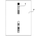
以下に、分光測色器10によるトナーパッチの測色動作について説明する。図3は、記録材Pに形成された測色用パッチ画像Tを示す概略図である。
分光測色器10によるトナーパッチの測色動作が開始されると、まず初めに前述した一連の画像形成動作により記録材Pに図3に示すような測色用パッチ画像Tが形成される。定着部51を通過した記録材Pは、排出部でのスイッチバック動作によって両面搬送路Dへと引き込まれ、両面搬送路D中に配置された分光測色器10にて、記録材Pに形成された測色用パッチ画像Tが、記録材Pの搬送と同期しながら順次測色される。その後、搬送ローラ対47を通過した記録材Pは、2次転写部・定着部51を通過して排出ローラ50によって排出トレイ52に排出される。
このような一連の画像形成動作は、画像形成装置内に設けられた制御部55によって制御動作される。
Hereinafter, the color measurement operation of the toner patch by the
When the color measurement operation of the toner patch by the
Such a series of image forming operations is controlled by a
次に、本実施例の画像形成装置における画像処理動作の一例を、図4に示すブロック図を用いて説明する。
画像形成装置のコントローラ部56と制御部55は、ビデオインターフェースで接続され、コントローラ部56が外部端末のホストコンピュータ57や不図示のネットワークに接続される。コントローラ部56の記憶手段には、色変換に用いるカラーマッチングテーブル(CM)、色分解テーブル(C1)、カラー補正テーブル(C2)が記憶されている。また、制御部55には、分光測色器10、画像形成処理や分光測色器10からの測色結
果を処理するCPU202と、計測結果を一時保管するメモリ203が搭載されている。
Next, an example of an image processing operation in the image forming apparatus of this embodiment will be described with reference to the block diagram shown in FIG.
The
画像形成動作が開始されると、次のような処理が行われる。
まず、コントローラ部56は予め用意されているカラーマッチングテーブル(CM)により、ホストコンピュータ等から送られてくる画像の色を表すRGB信号をカラー画像形成装置の色再現域に合わせたデバイスRGB信号(以下、DevRGB)に変換する。続いて色分解テーブル(C1)及び後述するカラー補正テーブル(C2)により、前記DevRGB信号をカラー画像形成装置のトナー色材色であるCMYK信号に変換する。そして、各々のカラー画像形成装置に固有の階調‐濃度特性を補正する濃度補正テーブル(D)により、前記CMYK信号を階調‐濃度特性の補正を加えたC’M’Y’K’信号へ変換する。その後ハーフトーン処理を行い、C’’M’’Y’’K’’信号へ変換した後に、PWMテーブル(PW)により、前記C’’M’’Y’’K’’信号に対応する露光光スキャナ部(33C、33M、33Y、33K)の露光時間Tc、Tm、Ty、Tkへ変換する。ここで、PWMは、パルス幅変調(Pulse Width Modulation)である。
コントローラ部56は、これら露光時間Tc、Tm、Ty、Tkに従って露光光スキャナ部33を制御することで、感光ドラム31C、31M、31Y、31Kの表面に静電潜像を形成し、先に述べた一連の画像形成動作が行われる。
When the image forming operation is started, the following processing is performed.
First, the
The
また、分光測色器10によるトナーパッチ画像の測色動作においては、予めカラーパッチデータとしてコントローラ部56に格納されている複数個のCMYK形式のカラーパッチデータ(CPD)に従って記録材Pに測色用パッチ画像Tが形成される。記録材上(被測色材上)に形成された測色用パッチ画像Tは、分光測色器10で測色され、それぞれのパッチ毎に分光反射率Or(λ)が読み取られ、制御演算部21cから出力される。
読み取られた分光反射率データは、制御部55によって色度値(例えば、CIEL*a*b*)に変換されてコントローラ部56の色変換部へ送られる。そして、不図示のCMS(カラーマネージメントシステム)を利用して、色度値が画像形成装置に依存するCMYK形式のデータ(CSD)に変換される。その後、前記変換されたCMYKデータ(CSD)と、デフォルトのカラーパッチデータ(CPD)を比較することによって、その差を補正するような補正テーブル(C2)が生成される。
Further, in the color measurement operation of the toner patch image by the
The read spectral reflectance data is converted into a chromaticity value (for example, CIE L * a * b *) by the
これらの処理は、測色された全ての測色用パッチに対して行われるが、測色されるパッチは画像形成装置で再現可能な全ての色を必ずしも揃えている必要はない。例えば、混色グレーのパッチを作成してグレー軸補正のみを行ってもよい。測色用パッチとして記録材Pに形成されていないCMYKデータに関しては、測色されたパッチを基に補間処理を行うことで補正テーブル(C2)を作成すればよい。このようにして作成された補正テーブル(C2)は色分解テーブル(C1)と共にコントローラ部56に更新・保持される。
These processes are performed on all colorimetric patches that have been colorimetrically measured, but the colorimetric patches need not necessarily have all colors that can be reproduced by the image forming apparatus. For example, a mixed gray patch may be created to perform only the gray axis correction. For CMYK data that is not formed on the recording material P as a colorimetric patch, a correction table (C2) may be created by performing an interpolation process based on the colorimetric patch. The correction table (C2) created in this way is updated and held in the
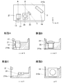
次に、本実施例の効果を明確にするための比較例について説明する。
図5は、比較例の分光測色器310の概略図である。なお、説明の便宜上、本実施例と同様の構成部分については同一の符号を付している。
比較例では、光源12が実装されている基板24と、ラインセンサ11が実装されている基板25が別基板となっている。
一方、前述したように本実施例の分光測色器10は、光源12とラインセンサ11が、同一の基板21上に実装されている。これにより、比較例のように基板24と基板25を各々組み立てる必要が無くなり、分光測色器10の組立時の作業性が向上し、結果としてコストの削減に寄与できる。
Next, a comparative example for clarifying the effect of the present embodiment will be described.
FIG. 5 is a schematic diagram of a
In the comparative example, the
On the other hand, as described above, in the
また、分光測色器においては、前述したように熱変形による検知精度低下が課題としてある。これは、分光測色器のハウジングに好適に使用されるモールド樹脂の熱変形(クリ
ープ)により、特にラインセンサ11の位置が変動することに起因するものである。ラインセンサ11の位置が変動することで、本来、検知されるべき分光波長とラインセンサ11の各画素との対応が変化してしまい、その結果、検知精度が低下してしまうことが懸念される。
Further, in the spectrocolorimeter, as described above, there is a problem of a decrease in detection accuracy due to thermal deformation. This is because the position of the
本実施例では、光源12とラインセンサ11が同一基板21に実装されており、本実施例の基板21の大きさは、比較例におけるラインセンサ11のみが実装されている基板25よりも大きい。基板21、25には、紙にエポキシ樹脂を含浸したもの、またはガラス繊維製の布を重ねエポキシ樹脂を含浸したものが好適に使用されており、熱変形(クリープ)による影響はモールド樹脂製のハウジングと比べ非常に小さい。よって、分光測色器において熱変形によりラインセンサ11の位置が変動することを抑制するには、本実施例の構成の方が比較例よりも有利となる。
In this embodiment, the
本実施例では、さらに、次のような効果が得られる。
ハウジングに好適に使用されるモールド樹脂として、ポリカーボネート、ABS(アクリロニトリル・ブタジエン・スチレン共重合体)、ポリエチレン、ポリプロピレン等がある。しかし、これらのモールド樹脂は、基板21に好適に使用される、紙にエポキシ樹脂を含浸したもの、またはガラス繊維製の布を重ねエポキシ樹脂を含浸したものに対し、引っ張り弾性率、曲げ強さは小さい。
よって、カラー画像形成装置の熱変形等により外部から力が加わった際、基板21が補強部材としての役割を発揮し、本実施例のように基板21の大きさが大きい方が、ラインセンサ11の位置変動を抑える効果が大きい。結果として、検知精度の低下を防止することが可能となる。
In the present embodiment, the following effects are further obtained.
Examples of the mold resin suitably used for the housing include polycarbonate, ABS (acrylonitrile / butadiene / styrene copolymer), polyethylene, and polypropylene. However, these mold resins are preferably used for the
Therefore, when a force is applied from the outside due to thermal deformation or the like of the color image forming apparatus, the
また、比較例のように、光源12が実装されている基板24と、ラインセンサ11が実装されている基板25が別基板となっている場合には、分光測色器310のハウジングが熱変形した場合に、基板24と基板25それぞれの位置が変動してしまうこととなる。このため、光源12とラインセンサ11の位置はそれぞれ別々に変動することとなり、検知精度の低下が大きくなってしまうことが懸念される。
これに対して本実施例では、光源12とラインセンサ11が同一の基板21に実装されているので、分光測色器10のハウジングが熱変形した場合、光源12とラインセンサ11は基板21の変動に従うこととなる。このため、本実施例では、光源12とラインセンサ11の位置がそれぞれ別々に変動してしまう比較例の場合よりも検知精度の低下を抑えることができる。
Further, as in the comparative example, when the
On the other hand, in the present embodiment, the
以上説明したように、本実施例では、光源12とラインセンサ11が同一基板21に実装されるので、光源12とラインセンサ11をそれぞれ実装するために別々に基板を用意する必要がなくなり、コストを下げることができる。また、同一基板21の適用により、分光測色器10の組み立ての際に、1つの基板をハウジングに組み付ければよくなり、組立作業性を改善することができる。その結果、コスト低減に寄与することができる。さらには、熱変形の影響を低減することができるので、検知精度の低下を防止することが可能となる。
さらに、分光測色器10を画像形成装置に搭載し、出力された測色用パッチを画像形成装置内に設置された分光測色器10によって読み取り、測色結果を画像形成条件にフィードバックさせることで、色再現性の良い出力物(画像)を得ることが可能となる。
As described above, in the present embodiment, since the
Further, the
次に、実施例2について説明する。なお、実施例1と同様の構成部分については同一の符号を付して、その説明は省略する。
本実施例では、回折格子18により分光されラインセンサ11に受光される光(分光光
束)の光路が、被測色物14の被検知面(表面)に略平行になるように、回折格子18及びラインセンサ11が配置されていることを特徴としている。つまり、回折格子18のローランド円(不図示)の中心軸はZ軸に平行で被検知面(表面)に直交している。
このために、本実施例では、回折格子18及びラインセンサ11が配置されている面(仮想面)と、被測色物14の被検知面とが略平行になるように構成されている。また、光源12とラインセンサ11が実装されている基板21表面(基板21のうち光源12とラインセンサ11が実装されている表面)と、被測色物14の被検知面とが互いに略垂直となるように構成されている。
Next, Example 2 will be described. In addition, the same code | symbol is attached | subjected about the component similar to Example 1, and the description is abbreviate | omitted.
In the present embodiment, the
Therefore, in this embodiment, the surface (virtual surface) on which the
図6は、本実施例の分光測色器210の概略構成を説明するための図である。図6(a)は、分光測色器210を被検知面に対して垂直方向(上側)から見た概略断面(XY断面)図である。また、図6(b)は、被測色物14の被検知面に対して垂直方向の断面(XZ断面)を示し、分光測色器210を正面側から見た図となっている。
本実施例の分光測色器210においては、被測色物14の被検知面に対して略垂直の関係にある基板21上の光源12からY方向に光15が発せられる。ここで、被測色物14の被検知面はXY平面上に存在し、基板21表面はXZ平面上に存在している。
Y方向に発せられた光15は、照射側の照射ライトガイド27により集光され、光源12の照射方向(Y方向)に対して平行関係にある被測色物14に、約45°の角度で入射するよう、照射ライトガイド27によりXZ平面上を進行するように方向を変えられる。被測色物14に約45°の角度で入射した光15は、被測色物14の光吸収特性に応じた散乱光となる。散乱光16の一部は、入射側の入射ライトガイド28に取り込まれ、平行光となった後、スリット22に入射するよう、XY平面上を進行するように方向を変えられる。そして、散乱光16はスリット22を通過し、回折格子18により分光され、XY平面に沿うように進んでラインセンサ11で検出される。
FIG. 6 is a diagram for explaining a schematic configuration of the
In the
The light 15 emitted in the Y direction is collected by the irradiation
このように本実施例では、回折格子18により分光されラインセンサ11で検出される光の光路と、被測色物14の被検知面とがそれぞれXY平面上に存在することで、互いに略平行の関係にある。一方、実施例1では、回折格子18により分光されラインセンサ11で検出される光の光路は、XZ平面上に存在しており、XY平面上に存在する被測色物14の被検知面に対して、略垂直の関係にあることが、本実施例と異なっている。ここで、実施例1では、基板21表面と、被測色物14の被検知面とが略平行となるように構成されている。
As described above, in this embodiment, the optical path of the light split by the
本実施例の分光測色器210のより具体的な構成について説明する。図11(a)はより具体的な構成を示すXY断面図である。図11(b)はより具体的な構成を示すXZ断面図である。これらの図に示すように、分光測色器210は、ハウシングを構成する筐体210aと蓋210bを有する。このハウジングの筐体210aに照射ライトガイド27、入射ライトガイド28、スリット22、回折格子18、及び、基板21がそれぞれ位置決め固定される。
次に、筐体210aに対する照射ライトガイド27、入射ライトガイド28、スリット22、回折格子18、の位置決め固定方法について説明する。図12は、分光測色器210をZ方向から見た概略図と、各断面での断面図である。断面Aは、照射ライトガイド27と筐体210aとの関係を示しており、照射ライトガイド27は、Y方向(矢印が向く方向)に筐体210aに突き当たった状態でその位置が決め、そのまま紫外線硬化接着剤によって筐体210aに固定される。その他の入射ライトガイド28(断面B)、スリット22(断面C)、回折格子18(断面D)も同様にY方向(矢印が向く方向)に筐体210aに突き当たった状態でその位置が決め、そのまま紫外線硬化接着剤によって筐体210aに固定される。
A more specific configuration of the
Next, a method for positioning and fixing the irradiation
次に、筐体210a、蓋210b、基板21との関係について詳しく説明する。図13
はハウジングの斜視図である。図13(a)は、分光測色器210のハウジングが組み立てられた状態を示す。図13(b)は、分光測色器210のハウジングが組み立てられる前の状態を示す図である。なお、内部に固定されている照射ライトガイド27、入射ライトガイド28、スリット22、回折格子18は不図示。これらの図からわかるように、筐体210aに対してZ方向で蓋210bが取り付けられ、Y方向で基板21が取り付けられる。蓋210bは筐体210aに設けられた溝に嵌ることでその位置が決まり、紫外線硬化接着剤によって固定される。一方基板21には、X方向及びZ方向の位置決めの基準となる基準穴21aが設けられ、筐体210aに設けられた不図示のボスと嵌合することで基板21のX方向及びZ方向の位置を決める。さらに、基板21には切欠き部21bが設けられ、この部分が筐体210aに設けられた不図示の凸部に嵌合することで、基板21のY軸回りの回転止めとなる。基板21は紫外線硬化接着剤によって筐体210bに固定される。
Next, the relationship between the
FIG. 3 is a perspective view of a housing. FIG. 13A shows a state in which the housing of the
ここで、回折格子18により波長分散された光を、ラインセンサ11で検出する際、波長分解能を確保するには、回折格子18からラインセンサ11までの光路に関して、ある程度の光路長が必要になる。
実施例1の構成では、回折格子18により分光されラインセンサ11で検出される光の光路がXZ平面上に存在し、被測色物14の被検知面に対して略垂直の関係にある。このため、被測色物14の被検知面に対して垂直方向(Z方向)においては、回折格子18からラインセンサ11までの光路長を所望の長さに設定する必要があり、分光測色器210のサイズ(寸法)を小さくすることが困難となることが懸念される。ここで、以下の説明では、被測色物14の被検知面に対して垂直方向(Z方向)における分光測色器210のサイズを、説明の便宜上、分光測色器210の高さ(被検知面と平行にある2面間の距離)という。
これに対して、本実施例においては、上述のように、回折格子18により分光されラインセンサ11で検出される光の光路がXY平面上に存在し、被測色物14の被検知面に略平行の関係にある。このため、本実施例では、分光測色器210の高さを、実施例1の構成よりも小さくすることが可能となる。
Here, when detecting the wavelength-dispersed light by the
In the configuration of the first embodiment, the optical path of the light that is split by the
On the other hand, in the present embodiment, as described above, the optical path of the light that is split by the
本実施例の画像形成装置においては、図2に示すように、分光測色器210が両面搬送路中の記録材Pに対向する位置に配置されている。このような構成において、分光測色器210の高さが小さくできることにより、画像形成装置の小型化が可能となり、また、分光測色器210が例えば2次転写ローラ43等の他部材と干渉してしまうことを懸念する必要がなくなり、設計の自由度を大きくできる。
In the image forming apparatus of this embodiment, as shown in FIG. 2, the
また、実施例1では、回折格子18により分光されラインセンサ11で検出される光の光路がXZ平面上に存在し、被測色物14の被検知面に対して略垂直の関係にある。このため、回折格子18からラインセンサ11までの光路長が所望の長さに設定された場合、光源12から被測色物14までの光路長が長くなってしまうことが懸念される。
これに対して、本実施例においては、分光測色器210の高さを、実施例1よりも小さくすることができるので、光源12から被測色物14までの光路長を実施例1よりも短くすることが可能となる。実施例1と比較すると、本実施例では光源12から被測色物14までの光路長を60%に短くすることができ、光源12の発光光量を略半減することができる。よって、本実施例では、被測色物14に照射する光量を確保するために発光光量を上げる必要がなくなり、電流を多く流す必要もなくなり、回路のコスト上昇、発光素子のコスト上昇を抑えることができ、結果、コストを低減することが可能となる。
In the first embodiment, the optical path of light that is split by the
On the other hand, in the present embodiment, the height of the
以上説明したように、本実施例によれば、光源12が実装されている基板21と、被検知面を略垂直の関係にすることで、実施例1の効果に加えて、分光測色器210における被検知面と垂直方向の高さを小さくすることが可能となる効果が得られる。さらには、光
源12から被測色物14までの光路長を短くすることができるので、分光測色器210のコストを低減することが可能となる。
ここで、本実施例では、回折格子18により分光されラインセンサ11で検出される光の光路は、XY平面上に存在し被測色物14の被検知面に略平行であるが、これに限らず、XY平面(被検知面に平行な仮想面)に沿うように構成されるものであればよい。
また、本実施例では、光源12とラインセンサ11が実装されている基板21表面と、被測色物14の被検知面とが互いに略垂直となるように構成されているが、これに限るものではない。すなわち、回折格子18により分光されラインセンサ11に受光されてラインセンサ11で検出される光の光路が、XY平面に沿うように構成されるものであれば、基板21表面と、被測色物14の被検知面との関係は互いに略垂直でなくてもよい。
また、本実施例の構成により、分光測色器210のサイズのうち分光測色器210の高さ(被測色物14の被検知面に対して垂直方向(Z方向)のサイズ)を抑えることが可能となった。これに対して、分光測色器210のサイズのうち分光測色器210における被測色物14の被検知面に平行な方向(Y方向)のサイズを抑えたい場合には、実施例1の構成を用いるとよい。
As described above, according to the present embodiment, the
Here, in this embodiment, the optical path of the light that is split by the
In the present embodiment, the surface of the
Further, with the configuration of this embodiment, the height of the spectrocolorimeter 210 (the size in the direction perpendicular to the detection surface of the color measurement object 14 (Z direction)) among the sizes of the
次に、実施例3について説明する。なお、実施例1,2と同様の構成部分については同一の符号を付して、その説明は省略する。
本実施例では、基板21上のうち光源12とラインセンサ11の間の領域が、光の伝達を低減させる(光源12から照射された光の一部が基板21を介してラインセンサ11に入射することを抑制する)光伝達低減構造となっていることを特徴とする。
Next, Example 3 will be described. In addition, the same code | symbol is attached | subjected about the component similar to Example 1, 2, and the description is abbreviate | omitted.
In the present embodiment, the region between the
図7は、基板21を示す概略図である。基板21上には、光源12とラインセンサ11が実装されている。また、基板21のうち光源12とラインセンサ11の間の領域には、穴26が設けられている。本実施例では、穴26としてスリットが設けられている。
FIG. 7 is a schematic view showing the
本実施例では、図7に示すように、高さ(図7で鉛直方向の長さ)が15mm、幅(図7で水平方向の長さ)が90mmの基板21上に、光源12とラインセンサ11を基板21の中心(図7で鉛直方向の中心)に配置した。さらに、高さ13mm、幅2mmの穴26を、図7における基板21の鉛直方向の中心位置であって、光源12からラインセンサ11方向に5mm離れた位置に設けた。
これにより、光源12から照射された光の一部(迷光)が基板21を介してラインセンサ11に入射することを低減することが可能となる。本実施例では、光源12から基板21を伝わりラインセンサ11に入射する迷光を、実施例1に対して98%低減することができた。
ここで、迷光の影響を受けた場合には、検知精度が低下してしまうことが懸念される。これは、回折格子18により分光された光以外に、外乱成分としての迷光をラインセンサ11が検出してしまうためである。特に、被測色物からの反射光が少なくなる明度の低いトナーパッチを測色する際、検知精度の低下が顕著となるので、迷光は極力抑制することが望ましい。
In the present embodiment, as shown in FIG. 7, a
Thereby, it becomes possible to reduce that a part of the light (stray light) emitted from the
Here, when affected by stray light, there is a concern that the detection accuracy may decrease. This is because the
次に、本実施例により迷光が低減できる理由について詳述する。
基板21は、紙にエポキシ樹脂を含浸したもの、またはガラス繊維製の布を重ねエポキシ樹脂を含浸したものが好適に使用される。このため、基板21は光を良く伝達する構造となっている。
このため、光源12から照射された光の一部が、照射側の照射ライトガイド19、27に入らず反射し、基板21に入射した場合、この光は、基板21内を伝わり、ラインセンサ11に迷光として検出されてしまう。また、照射側の照射ライトガイド19、27から出た光の一部が開口13へ向かって照射されず、分光測色器10、210内を反射し、基
板21に入射した場合、この光は、基板21内を伝わり、ラインセンサ11に迷光として検出されてしまう。
本実施例では、光源12とラインセンサ11の間の領域に、光伝達低減構造として穴26を設けているので、基板21を伝わる迷光を低減することができ、検知精度を向上することができる。
Next, the reason why stray light can be reduced by this embodiment will be described in detail.
As the
For this reason, when a part of the light emitted from the
In the present embodiment, since the
尚、光伝達低減構造としては、本構成に限らず、基板21のうち少なくとも、光源12とラインセンサ11の間の一部の領域が、光の伝達を低減する材質(材料)から成る部材で形成されることで、迷光の低減を図るものであってもよい。これに加えて、上述したような穴26を設けることで、更なる迷光の低減を図ってもよい。
基板21に用いる光伝達低減の材質としては、エポキシ樹脂に例えばカーボン粉末、グラファイト粉末等の着色剤を混合するのが好適である。また、基板21にアルミナ、窒化アルミ等のセラミックを用いるのも好適である。
The light transmission reduction structure is not limited to this configuration, and at least a part of the
As a material for reducing light transmission used for the
以上説明したように、本実施例によれば、基板21のうち光源12とラインセンサ11との間の領域に光伝達低減構造を設けることで、上述した実施例の効果に加えて、迷光による検知精度の低下を低減することが可能となる効果が得られる。
As described above, according to the present embodiment, by providing the light transmission reduction structure in the region between the
10…分光測色器、11…ラインセンサ、12…光源、14…被測色物、15…光、21…基板
DESCRIPTION OF
Claims (12)
前記発光素子により光を照射され被測色材で反射された光を波長毎に分光する回折格子と、
複数の画素を備え、前記回折格子により分光された光を前記複数の画素で波長毎に受光する受光素子と、
を有する測色装置において、
前記発光素子と前記受光素子とは、同一基板上の同一側面に配置されており、
前記回折格子により分光され前記受光素子に受光される光の光路が、被測色材の表面に平行な仮想面に沿うように、前記回折格子と前記受光素子とが配置されていることを特徴とする測色装置。 A light emitting element for irradiating light on the surface of the color material to be measured;
A diffraction grating that divides the light irradiated by the light emitting element and reflected by the color material to be measured for each wavelength;
A light receiving element comprising a plurality of pixels, and receiving light separated by the diffraction grating for each wavelength by the plurality of pixels;
In a color measuring device having
The light emitting element and the light receiving element are disposed on the same side surface on the same substrate ,
The diffraction grating and the light receiving element are arranged so that an optical path of light split by the diffraction grating and received by the light receiving element is along a virtual plane parallel to the surface of the color material to be measured. Color measuring device.
前記発光素子により光を照射され被測色材で反射された光を波長毎に分光する回折格子と、A diffraction grating that divides the light irradiated by the light emitting element and reflected by the color material to be measured for each wavelength;
複数の画素を備え、前記回折格子により分光された光を前記複数の画素で波長毎に受光する受光素子と、A light receiving element comprising a plurality of pixels, and receiving light separated by the diffraction grating for each wavelength by the plurality of pixels;
を有する測色装置において、In a color measuring device having
前記発光素子と前記受光素子とは、同一基板上の同一側面に配置され、The light emitting element and the light receiving element are disposed on the same side surface on the same substrate,
前記基板に垂直な方向に見たときに、前記複数の画素における画素の並ぶ方向と、前記発光素子、前記回折格子及び前記受光素子の並ぶ方向と、が平行であることを特徴とする測色装置。When viewed in a direction perpendicular to the substrate, the direction in which the pixels of the plurality of pixels are arranged is parallel to the direction in which the light emitting element, the diffraction grating, and the light receiving element are arranged. apparatus.
伝達しにくい材質の部分が設けられていることを特徴とする請求項1乃至3のいずれか一項に記載の測色装置。 4. The substrate according to claim 1, wherein a portion made of a material that is less likely to transmit light than other portions of the substrate is provided between the light emitting element and the light receiving element. The color measuring device according to claim 1.
前記発光素子から照射された光を前記被測色材に導光する第1導光手段と、
前記被測色材で反射された光を前記回折格子に導光する第2導光手段と、を備え、
前記ハウジングには、前記第1導光手段と、前記第2導光手段と、前記回折格子が配置されていることを特徴とする請求項1乃至6のいずれか一項に記載の測色装置。 A housing for positioning the substrate;
First light guiding means for guiding light emitted from the light emitting element to the color material to be measured;
A second light guide means for guiding the light reflected by the color material to be measured to the diffraction grating,
The colorimetric apparatus according to any one of claims 1 to 6, wherein the first light guide unit, the second light guide unit, and the diffraction grating are arranged in the housing. .
記録材上に画像を形成する画像形成手段と、
制御手段と、
を有し、被測色材としての記録材に前記発光素子から光を照射し、前記記録材で反射された光を前記回折格子によって波長毎に分光して前記受光素子で受光し、前記制御手段が前記受光素子の出力に基づいて前記画像形成手段の画像形成条件を調整することを特徴とする画像形成装置。 A colorimetric device according to any one of claims 1 to 11,
Image forming means for forming an image on a recording material;
Control means;
The recording material as a color material to be measured is irradiated with light from the light emitting element, the light reflected by the recording material is spectrally separated by the diffraction grating for each wavelength, and received by the light receiving element, and the control An image forming apparatus characterized in that the means adjusts an image forming condition of the image forming means based on an output of the light receiving element.
Priority Applications (4)
| Application Number | Priority Date | Filing Date | Title |
|---|---|---|---|
| JP2013147644A JP6278625B2 (en) | 2012-07-30 | 2013-07-16 | Color measuring device and image forming apparatus having the same |
| US13/951,869 US20140029963A1 (en) | 2012-07-30 | 2013-07-26 | Colorimetry apparatus and image forming apparatus |
| US15/460,364 US10359315B2 (en) | 2012-07-30 | 2017-03-16 | Colorimetry apparatus and image forming apparatus |
| US16/282,339 US10837835B2 (en) | 2012-07-30 | 2019-02-22 | Colorimetry apparatus and image forming apparatus |
Applications Claiming Priority (3)
| Application Number | Priority Date | Filing Date | Title |
|---|---|---|---|
| JP2012168501 | 2012-07-30 | ||
| JP2012168501 | 2012-07-30 | ||
| JP2013147644A JP6278625B2 (en) | 2012-07-30 | 2013-07-16 | Color measuring device and image forming apparatus having the same |
Publications (3)
| Publication Number | Publication Date |
|---|---|
| JP2014044199A JP2014044199A (en) | 2014-03-13 |
| JP2014044199A5 JP2014044199A5 (en) | 2016-09-01 |
| JP6278625B2 true JP6278625B2 (en) | 2018-02-14 |
Family
ID=49995001
Family Applications (1)
| Application Number | Title | Priority Date | Filing Date |
|---|---|---|---|
| JP2013147644A Active JP6278625B2 (en) | 2012-07-30 | 2013-07-16 | Color measuring device and image forming apparatus having the same |
Country Status (2)
| Country | Link |
|---|---|
| US (3) | US20140029963A1 (en) |
| JP (1) | JP6278625B2 (en) |
Families Citing this family (14)
| Publication number | Priority date | Publication date | Assignee | Title |
|---|---|---|---|---|
| JP6251073B2 (en) | 2014-02-05 | 2017-12-20 | 浜松ホトニクス株式会社 | Spectrometer and method of manufacturing the spectrometer |
| JP6370091B2 (en) * | 2014-04-28 | 2018-08-08 | キヤノン株式会社 | Image forming apparatus and detection apparatus |
| CN106574897B (en) * | 2014-06-10 | 2020-02-14 | 赛诺菲-安万特德国有限公司 | Apparatus for determining information related to surface reflection characteristics |
| US10663348B2 (en) * | 2014-12-08 | 2020-05-26 | Konica Minolta, Inc. | Colorimetric sensor device and image formation apparatus |
| US10728424B2 (en) * | 2015-01-13 | 2020-07-28 | Canon Kabushiki Kaisha | Color measuring apparatus and image forming apparatus |
| JP6652295B2 (en) * | 2015-01-13 | 2020-02-19 | キヤノン株式会社 | Colorimetric device and image forming device |
| EP3372966B1 (en) * | 2017-03-10 | 2021-09-01 | Hitachi High-Tech Analytical Science Limited | A portable analyzer using optical emission spectoscopy |
| CN108968112B (en) | 2017-06-01 | 2021-05-18 | 志勇无限创意股份有限公司 | Bean drying device |
| EP3657204A4 (en) * | 2017-07-18 | 2021-04-28 | Pioneer Corporation | Optical device |
| JP2019159203A (en) * | 2018-03-15 | 2019-09-19 | 株式会社リコー | Optical member, projection device, head-mounted display, head-up display, vehicle, spectrometer, and image forming apparatus |
| US11639873B2 (en) * | 2020-04-15 | 2023-05-02 | Viavi Solutions Inc. | High resolution multi-pass optical spectrum analyzer |
| JP2022077576A (en) * | 2020-11-12 | 2022-05-24 | セイコーエプソン株式会社 | Color measuring device |
| JP2022077753A (en) * | 2020-11-12 | 2022-05-24 | セイコーエプソン株式会社 | Color measuring device |
| JP2022143831A (en) * | 2021-03-18 | 2022-10-03 | セイコーエプソン株式会社 | Color measurement device |
Family Cites Families (67)
| Publication number | Priority date | Publication date | Assignee | Title |
|---|---|---|---|---|
| JPH02103426A (en) * | 1988-10-12 | 1990-04-16 | Kuraray Co Ltd | Color sensor |
| US5262840A (en) * | 1990-01-30 | 1993-11-16 | Sequa Corporation | Multispectral reflectometer |
| US5476108A (en) * | 1990-04-05 | 1995-12-19 | R. J. Reynolds Tobacco Company | Method and apparatus for detecting foreign matter within a layer of tabacco |
| US5489980A (en) * | 1992-03-18 | 1996-02-06 | Anthony; Michael | Apparatus for rapid and accurate analysis of the composition of samples |
| US5319433A (en) | 1992-05-18 | 1994-06-07 | Canon Kabushiki Kaisha | Electrophotographing apparatus for forming color image |
| JPH0611943A (en) | 1992-06-26 | 1994-01-21 | Canon Inc | Image forming device |
| JPH0811943A (en) | 1994-06-28 | 1996-01-16 | Nidaiki Kk | Air permeable bag to prevent germs from entering |
| DE4434168B4 (en) * | 1994-09-24 | 2004-12-30 | Byk-Gardner Gmbh | Device and method for measuring and evaluating spectral radiation and in particular for measuring and evaluating color properties |
| US7119337B1 (en) * | 1997-08-04 | 2006-10-10 | Ion Optics, Inc. | Infrared radiation sources, sensors and source combinations, and methods of manufacture |
| US5737113A (en) | 1995-08-04 | 1998-04-07 | Canon Kabushiki Kaisha | Optical modulators and color image display device employing the same |
| DK0918984T3 (en) * | 1996-08-16 | 2001-10-22 | Zeptosens Ag | Optical detection device |
| US5880834A (en) * | 1996-10-16 | 1999-03-09 | The United States Of America As Represented By The Administrator Of The National Aeronautics And Space Administration | Convex diffraction grating imaging spectrometer |
| US6560019B2 (en) | 1998-02-05 | 2003-05-06 | Canon Kabushiki Kaisha | Diffractive optical element and optical system having the same |
| JP4336412B2 (en) | 1998-06-16 | 2009-09-30 | キヤノン株式会社 | Diffractive optical element and optical system using the same |
| JP3787474B2 (en) | 1998-12-24 | 2006-06-21 | キヤノン株式会社 | Method for setting two design wavelengths in a diffractive optical element |
| US6424416B1 (en) * | 1999-10-25 | 2002-07-23 | Textron Systems Corporation | Integrated optics probe for spectral analysis |
| US6836325B2 (en) * | 1999-07-16 | 2004-12-28 | Textron Systems Corporation | Optical probes and methods for spectral analysis |
| JP3530776B2 (en) | 1999-07-28 | 2004-05-24 | キヤノン株式会社 | Diffractive optical element and optical system using the same |
| JP3564027B2 (en) * | 2000-02-01 | 2004-09-08 | シャープ株式会社 | Optical coupling device and manufacturing method thereof |
| JP2001235368A (en) * | 2000-02-24 | 2001-08-31 | Matsushita Electric Works Ltd | Micro spectrometer |
| US6449045B1 (en) * | 2000-05-01 | 2002-09-10 | Xerox Corporation | System and method from reconstruction of spectral curves using measurements for a color sensor and statistical techniques |
| US6650477B2 (en) | 2000-06-07 | 2003-11-18 | Canon Kabushiki Kaisha | Diffractive optical element and optical apparatus having the same |
| US6657197B2 (en) * | 2000-12-22 | 2003-12-02 | Honeywell International Inc. | Small profile spectrometer |
| US6515752B2 (en) * | 2000-12-28 | 2003-02-04 | Coretek, Inc. | Wavelength monitoring system |
| US6764158B2 (en) * | 2001-10-02 | 2004-07-20 | Hewlett-Packard Development Company, L.P. | Compact optical sensing system |
| JP3870057B2 (en) | 2001-10-04 | 2007-01-17 | キヤノン株式会社 | Image forming apparatus |
| DE50115561D1 (en) * | 2001-11-26 | 2010-08-26 | X Rite Europe Gmbh | Spectrophotometer and use thereof |
| JP2004309146A (en) * | 2003-04-02 | 2004-11-04 | Olympus Corp | Spectrophotometer |
| US7315378B2 (en) * | 2003-06-04 | 2008-01-01 | Inverness Medical Switzerland Gmbh | Optical arrangement for assay reading device |
| JP2005164300A (en) * | 2003-11-28 | 2005-06-23 | Nippon Aleph Corp | Color sensor |
| JP2005172568A (en) * | 2003-12-10 | 2005-06-30 | Canon Inc | Optical device and measuring device having same |
| US7067819B2 (en) * | 2004-05-14 | 2006-06-27 | Kla-Tencor Technologies Corp. | Systems and methods for measurement or analysis of a specimen using separated spectral peaks in light |
| US7359052B2 (en) * | 2004-05-14 | 2008-04-15 | Kla-Tencor Technologies Corp. | Systems and methods for measurement of a specimen with vacuum ultraviolet light |
| JP4422039B2 (en) | 2005-01-31 | 2010-02-24 | ニチコン株式会社 | Toner adhesion measuring device |
| US7518380B2 (en) * | 2005-05-17 | 2009-04-14 | Honeywell International Inc. | Chemical impedance detectors for fluid analyzers |
| US20070013904A1 (en) * | 2005-07-15 | 2007-01-18 | Chia Chee W | Apparatus and system for characterizing a target |
| US7495761B2 (en) * | 2006-02-03 | 2009-02-24 | Foster-Miller, Inc. | Array detector coupled spectroanalytical system and graded blaze angle grating |
| JP5016855B2 (en) * | 2006-06-15 | 2012-09-05 | キヤノン株式会社 | Spectrometer and spectroscopic method |
| US7602496B2 (en) * | 2006-10-19 | 2009-10-13 | Sporian Microsystems, Inc. | Optical sensor with biologically reactive surface |
| JP2009008471A (en) | 2007-06-27 | 2009-01-15 | Canon Inc | Optical spectrometer and optical apparatus using same |
| US20090008471A1 (en) * | 2007-07-02 | 2009-01-08 | Chadwick Loring Wilson | Control Devices For Irrigation Systems |
| US8284401B2 (en) * | 2007-07-10 | 2012-10-09 | Nanolambda, Inc. | Digital filter spectrum sensor |
| US7869036B2 (en) * | 2007-08-31 | 2011-01-11 | Canon Kabushiki Kaisha | Analysis apparatus for analyzing a specimen by obtaining electromagnetic spectrum information |
| US7817274B2 (en) * | 2007-10-05 | 2010-10-19 | Jingyun Zhang | Compact spectrometer |
| US8345226B2 (en) * | 2007-11-30 | 2013-01-01 | Jingyun Zhang | Spectrometers miniaturized for working with cellular phones and other portable electronic devices |
| DE102008019600B4 (en) * | 2008-04-18 | 2021-03-04 | Fraunhofer-Gesellschaft zur Förderung der angewandten Forschung e.V. | Stacked optical device and method of making the same |
| US8482381B2 (en) * | 2008-07-31 | 2013-07-09 | Palm, Inc. | Multi-purpose detector-based input feature for a computing device |
| JP5453856B2 (en) | 2009-03-11 | 2014-03-26 | 株式会社リコー | Image forming apparatus, image forming method, program, and recording medium |
| JP5440110B2 (en) * | 2009-03-30 | 2014-03-12 | 株式会社リコー | Spectral characteristic acquisition apparatus, spectral characteristic acquisition method, image evaluation apparatus, and image forming apparatus |
| JP5424957B2 (en) * | 2009-04-30 | 2014-02-26 | キヤノン株式会社 | Spectral colorimetry apparatus and image forming apparatus using the same |
| JP5663900B2 (en) * | 2010-03-05 | 2015-02-04 | セイコーエプソン株式会社 | Spectroscopic sensor device and electronic device |
| JP5537194B2 (en) * | 2010-03-05 | 2014-07-02 | キヤノン株式会社 | Color image forming apparatus |
| JP5402740B2 (en) * | 2010-03-15 | 2014-01-29 | 株式会社リコー | Spectral characteristic acquisition device, image evaluation device, and image forming device |
| JP5605687B2 (en) | 2010-06-29 | 2014-10-15 | 株式会社リコー | Spectral characteristic measuring method, spectral characteristic measuring apparatus, and image forming apparatus having the same |
| CN102401796B (en) * | 2010-09-09 | 2017-02-01 | 艾博生物医药(杭州)有限公司 | Device for reading assay result from assay carrier |
| US8461513B2 (en) * | 2010-09-28 | 2013-06-11 | Texas Advanced Optoelectronic Solutions, Inc. | Method and apparatus for device with minimized optical cross-talk |
| EP2447686B1 (en) * | 2010-10-28 | 2014-05-21 | Canon Kabushiki Kaisha | Spectral colorimetric apparatus and image forming apparatus including the same |
| US8941062B2 (en) * | 2010-11-16 | 2015-01-27 | 1087 Systems, Inc. | System for identifying and sorting living cells |
| US8604436B1 (en) * | 2011-03-24 | 2013-12-10 | Maxim Integrated Products, Inc. | Proximity sensor device |
| JP5744655B2 (en) * | 2011-07-15 | 2015-07-08 | キヤノン株式会社 | Spectral color sensor and image forming apparatus |
| JP6051543B2 (en) * | 2012-03-09 | 2016-12-27 | 株式会社リコー | Spectroscopic measurement apparatus, image evaluation apparatus, and image forming apparatus |
| JP5910989B2 (en) * | 2012-03-09 | 2016-04-27 | 株式会社リコー | Spectroscopic measurement apparatus, image evaluation apparatus, and image forming apparatus |
| US20120176599A1 (en) * | 2012-03-16 | 2012-07-12 | Hong Kong Applied Science And Technology Research Institute Co. Ltd. | Optical transceiver |
| CH709865A1 (en) * | 2014-07-11 | 2016-01-15 | Tecan Trading Ag | Spectrometer with monochromator and order-sorting filter. |
| CA2904850C (en) * | 2014-09-22 | 2021-04-20 | Ngp Inc. | Analytes monitoring by differential swept wavelength absorption spectroscopy methods |
| US10728424B2 (en) * | 2015-01-13 | 2020-07-28 | Canon Kabushiki Kaisha | Color measuring apparatus and image forming apparatus |
| JP6918481B2 (en) * | 2016-12-16 | 2021-08-11 | キヤノン株式会社 | Image reader |
-
2013
- 2013-07-16 JP JP2013147644A patent/JP6278625B2/en active Active
- 2013-07-26 US US13/951,869 patent/US20140029963A1/en not_active Abandoned
-
2017
- 2017-03-16 US US15/460,364 patent/US10359315B2/en active Active
-
2019
- 2019-02-22 US US16/282,339 patent/US10837835B2/en active Active
Also Published As
| Publication number | Publication date |
|---|---|
| US20140029963A1 (en) | 2014-01-30 |
| US20170184454A1 (en) | 2017-06-29 |
| US20190186997A1 (en) | 2019-06-20 |
| US10359315B2 (en) | 2019-07-23 |
| US10837835B2 (en) | 2020-11-17 |
| JP2014044199A (en) | 2014-03-13 |
Similar Documents
| Publication | Publication Date | Title |
|---|---|---|
| JP6278625B2 (en) | Color measuring device and image forming apparatus having the same | |
| JP5537194B2 (en) | Color image forming apparatus | |
| US9165227B2 (en) | Color image forming apparatus | |
| US9066052B2 (en) | Image forming apparatus for forming a measurement image on a sheet | |
| CN102968011B (en) | Image forming apparatus, image forming method, and document management system | |
| US8908243B2 (en) | Image forming apparatus for measuring fixed image | |
| EP1311110B1 (en) | Method of making correction for color sensor output values in color image forming apparatus | |
| US20140125982A1 (en) | Image forming apparatus | |
| US9097587B2 (en) | Image forming apparatus for forming a measurement image | |
| JP5600477B2 (en) | Printing apparatus, measuring apparatus, and control method thereof | |
| JP7140592B2 (en) | Measuring device, image forming device | |
| US8989605B2 (en) | Image forming apparatus | |
| JP6468752B2 (en) | Color measuring device, image forming apparatus, and color measuring method | |
| JP5586652B2 (en) | Image processing apparatus and automatic gradation correction method | |
| KR100882288B1 (en) | Image forming apparatus and image forming method | |
| JP6669383B2 (en) | Measuring device, image forming device and image measuring device | |
| JP5921318B2 (en) | Image forming apparatus | |
| JP4502373B2 (en) | Image forming apparatus and control method thereof | |
| JP5253602B2 (en) | Image output apparatus and image output method | |
| US20220417375A1 (en) | Image reading apparatus and image forming apparatus | |
| JP2009068842A (en) | Photodetector | |
| JP2005027276A (en) | Image forming method and its apparatus | |
| JP2020048088A (en) | Measuring apparatus, image formation device and image formation system | |
| JP2013171212A (en) | Light detection device and image formation device | |
| JP2013205463A (en) | Image formation |
Legal Events
| Date | Code | Title | Description |
|---|---|---|---|
| A521 | Request for written amendment filed |
Free format text: JAPANESE INTERMEDIATE CODE: A523 Effective date: 20160714 |
|
| A621 | Written request for application examination |
Free format text: JAPANESE INTERMEDIATE CODE: A621 Effective date: 20160714 |
|
| A977 | Report on retrieval |
Free format text: JAPANESE INTERMEDIATE CODE: A971007 Effective date: 20170526 |
|
| A131 | Notification of reasons for refusal |
Free format text: JAPANESE INTERMEDIATE CODE: A131 Effective date: 20170606 |
|
| A521 | Request for written amendment filed |
Free format text: JAPANESE INTERMEDIATE CODE: A523 Effective date: 20170802 |
|
| TRDD | Decision of grant or rejection written | ||
| A01 | Written decision to grant a patent or to grant a registration (utility model) |
Free format text: JAPANESE INTERMEDIATE CODE: A01 Effective date: 20171219 |
|
| A61 | First payment of annual fees (during grant procedure) |
Free format text: JAPANESE INTERMEDIATE CODE: A61 Effective date: 20180116 |
|
| R151 | Written notification of patent or utility model registration |
Ref document number: 6278625 Country of ref document: JP Free format text: JAPANESE INTERMEDIATE CODE: R151 |