JP5684076B2 - Analog to digital converter and radio receiver - Google Patents
Analog to digital converter and radio receiver Download PDFInfo
- Publication number
- JP5684076B2 JP5684076B2 JP2011193965A JP2011193965A JP5684076B2 JP 5684076 B2 JP5684076 B2 JP 5684076B2 JP 2011193965 A JP2011193965 A JP 2011193965A JP 2011193965 A JP2011193965 A JP 2011193965A JP 5684076 B2 JP5684076 B2 JP 5684076B2
- Authority
- JP
- Japan
- Prior art keywords
- analog
- digital
- digital converter
- sampling
- output
- Prior art date
- Legal status (The legal status is an assumption and is not a legal conclusion. Google has not performed a legal analysis and makes no representation as to the accuracy of the status listed.)
- Expired - Fee Related
Links
Images


Classifications
-
- H—ELECTRICITY
- H03—ELECTRONIC CIRCUITRY
- H03M—CODING; DECODING; CODE CONVERSION IN GENERAL
- H03M1/00—Analogue/digital conversion; Digital/analogue conversion
- H03M1/06—Continuously compensating for, or preventing, undesired influence of physical parameters
- H03M1/08—Continuously compensating for, or preventing, undesired influence of physical parameters of noise
- H03M1/0836—Continuously compensating for, or preventing, undesired influence of physical parameters of noise of phase error, e.g. jitter
-
- H—ELECTRICITY
- H03—ELECTRONIC CIRCUITRY
- H03M—CODING; DECODING; CODE CONVERSION IN GENERAL
- H03M1/00—Analogue/digital conversion; Digital/analogue conversion
- H03M1/12—Analogue/digital converters
-
- H—ELECTRICITY
- H03—ELECTRONIC CIRCUITRY
- H03M—CODING; DECODING; CODE CONVERSION IN GENERAL
- H03M1/00—Analogue/digital conversion; Digital/analogue conversion
- H03M1/12—Analogue/digital converters
- H03M1/1205—Multiplexed conversion systems
- H03M1/121—Interleaved, i.e. using multiple converters or converter parts for one channel
- H03M1/1215—Interleaved, i.e. using multiple converters or converter parts for one channel using time-division multiplexing
Landscapes
- Engineering & Computer Science (AREA)
- Theoretical Computer Science (AREA)
- Analogue/Digital Conversion (AREA)
- Stabilization Of Oscillater, Synchronisation, Frequency Synthesizers (AREA)
Description
本発明は、デジタル補正機能付のアナログデジタル変換器及び当該アナログデジタル変換器を搭載する無線受信機に関する。 The present invention relates to an analog-digital converter with a digital correction function and a wireless receiver equipped with the analog-digital converter.
次世代の半導体検査装置や半導体製造装置に代表される産業用高度計測途の分野、ソフトウェア無線、コグニティブ無線に代表される次世代の無線通信システムの分野等においては、10ビット以上の高い有効分解能と1GS/s以上の極めて高い変換レートを両立できるアナログデジタル変換器が要求される。 High effective resolution of 10 bits or more in the field of industrial advanced measurement represented by next-generation semiconductor inspection equipment and semiconductor manufacturing equipment, and the field of next-generation wireless communication systems represented by software defined radio and cognitive radio And an analog-digital converter that can achieve both an extremely high conversion rate of 1 GS / s or more are required.
このような超高速かつ高分解能のアナログデジタル変換器の実現には、アナログデジタル変換器を構成するアナログ回路部が有する様々な非理想的な性質をデジタル補正する必要がある。このうち、アナログ回路内のアンプの利得不足(非特許文献1、2)やアナログデジタル変換器のサンプリングタイミングの静的な時間ずれであるスキューの影響(非特許文献3、4)を補正する技術については、従来より様々な技術が提案されている。
In order to realize such an ultra-high-speed and high-resolution analog-digital converter, it is necessary to digitally correct various non-ideal properties of the analog circuit unit constituting the analog-digital converter. Among these, a technique for correcting the effect of the skew (Non-Patent Documents 3 and 4), which is a lack of gain (
しかし、サンプリングタイミングのランダムな時間ずれであるジッタの影響は、そのランダムな性質ゆえにLMS(Least Mean Square)アルゴリズムなどによる適応制御を用いる補正が困難である。例えば10ビット以上の有効分解能を1GS/sの変換レートにおいて実現するためには、サンプリングクロックのジッタが1ps rms程度以下である必要がある。なお、rmsは、2乗平均値の平方根である。 However, the influence of jitter, which is a random time difference in sampling timing, is difficult to correct using adaptive control based on an LMS (Least Mean Square) algorithm or the like because of its random nature. For example, in order to realize an effective resolution of 10 bits or more at a conversion rate of 1 GS / s, the jitter of the sampling clock needs to be about 1 ps rms or less. Note that rms is the square root of the mean square value.
このような低ジッタのクロックを、1GS/sの高周波で、かつ、十分に低消費電力で実現することは困難である。すなわち、現状では、サンプリングクロックに含まれるジッタが、超高速、かつ、高分解能のアナログデジタル変換器の実現を困難にしている。 It is difficult to realize such a low jitter clock with a high frequency of 1 GS / s and sufficiently low power consumption. In other words, at present, jitter included in the sampling clock makes it difficult to realize an ultra-high speed and high resolution analog-digital converter.
前述したサンプリングクロックのジッタによるアナログデジタル変換器の有効分解能の劣化を軽減するために、特許文献1には、ジッタによる影響をアナログデジタル変換器の出力側においてデジタル補正する仕組が開示されている。図1に、当該仕組みを採用するアナログデジタル変換器を示す。以下に、アナログデジタル変換器10の構成を簡単に説明する。
In order to reduce the deterioration of the effective resolution of the analog-digital converter due to the jitter of the sampling clock described above,
アナログデジタル変換器10は、位相同期ループ(PLL:Phase Locked Loop)11と、分周器12と、アナログデジタル変換部13と、時間デジタル変換器(TDC:Time to Digital Converter)14と、デジタル補正部15で構成される。
The analog-
このアナログデジタル変換器10は、水晶発振器の出力等を源振とする位相同期ループ(PLL)11の出力を分周器12により分周し、分周後のクロック信号をサンプリングクロック(ADC CLK)としてアナログデジタル変換部13に供給する。アナログデジタル変換部13は、サンプリングクロックを用いて入力アナログ電圧をサンプリングし、サンプリング電圧をアナログデジタル変換して出力する。ただし、このアナログデジタル変換部13の出力値には、サンプリングクロックのジッタの影響が含まれている。
The analog-to-
そこで、アナログデジタル変換器10は、サンプリングクロックとPLL11の出力とを時間デジタル変換器14に入力し、各電圧遷移タイミングにおけるサンプリングクロックとPLL出力間の時間差(ジッタ値)をデジタル補正部15に与えてジッタの影響を補正する仕組みを採用する。
Therefore, the analog-
時間デジタル変換器14の研究開発は近年盛んであり、例えば非特許文献5には、1ps程度の時間分解能を有するものが開示されている。時間デジタル変換器14は、位相同期ループ11の出力が十分無視できるほど低ジッタであるものとし、同出力を基準に、サンプリングクロックに含まれるジッタ値を検出する。
Research and development of the time
デジタル補正部15は、時間デジタル変換器14において検出された時間差(ジッタ値)から各サンプリングタイミングにおけるサンプリング電圧誤差を推測し、その推測結果に基づいてアナログデジタル変換部13の生デジタル出力を補正する。このような仕組みにより、引用文献1のアナログデジタル変換器10は、アナログデジタル変換部13の生デジタル出力からサンプリングクロックに含まれるジッタの影響を取り除いている。
The
前述した特許文献1が開示する回路構成は、位相同期ループ11の出力の周波数及び周期が、アナログデジタル変換部13のサンプリングクロックよりも高周波、かつ、短周期であることに着目する。すなわち、同回路構成は、位相同期ループ11の出力に含まれるジッタが、サンプリングクロックのそれよりも小さくなることを利用する。
The circuit configuration disclosed in
しかしながら、位相同期ループ11をサンプリングクロックよりも高周波で動作させるには、大きな消費電力を必要とする。例えば特許文献1の場合、250MHzのサンプリングクロックに対し、位相同期ループの出力は8GHzと遥かに高周波である。これは、サンプリングクロックが1GHzの場合に、位相同期ループの出力が32GHzもの高周波になる換算であり、大きな消費電力と困難な高周波回路実装が必要になる。従って、特許文献1に開示されたアナログデジタル変換器を、次世代の産業用高度計測用途や無線通信システムで要求される超高速かつ高分解能のアナログデジタル変換器に適用することは困難である。
However, large power consumption is required to operate the phase-locked loop 11 at a higher frequency than the sampling clock. For example, in
上述の通り、サンプリングクロックに含まれるジッタの影響を、より低消費電力でデジタル補正することができるアナログデジタル変換器の実用化が求められている。 As described above, there is a demand for practical use of an analog-to-digital converter that can digitally correct the influence of jitter included in a sampling clock with lower power consumption.
そこで、本発明者は、以下の各部を有するアナログデジタル変換器を提供する。
(1) 基準クロックを源振とし、前記基準クロックより高周波数であり、かつ、前記基準クロックと同期したサンプリングクロックを生成する位相同期ループ
(2) 前記入力アナログ電圧を前記サンプリングクロックを用いてサンプリングし、デジタル値に変換するアナログデジタル変換部
(3) 前記基準クロックの電圧遷移タイミングに対する前記サンプリングクロックの時間遷移タイミングの時間差を検出し、前記時間差を差分デジタル値に変換する時間デジタル変換器
(4) 前記差分デジタル値を補間して各サンプリングタイミングに対応する補間値を求め、前記補間値により前記アナログデジタル変換部の生デジタル出力に含まれる前記サンプリングクロックのジッタの影響をデジタル補正するデジタル補正部
Therefore, the present inventor provides an analog-digital converter having the following units.
(1) A phase-locked loop that generates a sampling clock having a reference clock as a source and having a higher frequency than the reference clock and synchronized with the reference clock
(2) An analog-to-digital converter that samples the input analog voltage using the sampling clock and converts it to a digital value
(3) A time digital converter that detects a time difference in time transition timing of the sampling clock with respect to a voltage transition timing of the reference clock and converts the time difference into a differential digital value.
(4) A digital that interpolates the difference digital value to obtain an interpolation value corresponding to each sampling timing, and digitally corrects the influence of jitter of the sampling clock included in the raw digital output of the analog-to-digital conversion unit by the interpolation value Correction unit
本発明によれば、アナログデジタル変換器で使用するサンプリングクロックのジッタの影響を、低消費電力によりデジタル補正することができる。この結果、1GS/s以上の超高速で、10bit以上の高分解能を両立するアナログデジタル変換器を実現できる。 上記した以外の課題、構成及び効果は、以下の実施形態の説明により明らかにされる。 According to the present invention, the influence of jitter of a sampling clock used in an analog-digital converter can be digitally corrected with low power consumption. As a result, it is possible to realize an analog-to-digital converter that achieves both high resolution of 10 bits or more at an ultrahigh speed of 1 GS / s or more. Problems, configurations, and effects other than those described above will be clarified by the following description of embodiments.
以下の実施の形態においては、便宜上その必要があるときは、複数のセクションまたは実施の形態に分割して説明する。特に明示した場合を除き、それらは互いに無関係ではなく、一方は他方の一部または全部の変形例、応用例、詳細説明、補足説明等の関係にある。また、以下の実施の形態において、要素の数等(個数、数値、量、範囲等を含む)に言及する場合、特に明示した場合および原理的に明らかに特定の数に限定される場合等を除き、その特定の数に限定されるものではなく、特定の数以上でも以下でもよい。 In the following embodiment, when it is necessary for the sake of convenience, the description will be divided into a plurality of sections or embodiments. Unless otherwise specified, they are not irrelevant to each other, and one is in the relationship of some or all of the other, modification, application, detailed explanation, supplementary explanation, and the like. Further, in the following embodiments, when referring to the number of elements (including the number, numerical value, quantity, range, etc.), especially when clearly indicated and when clearly limited to a specific number in principle, etc. Except, it is not limited to the specific number, and may be more or less than the specific number.
さらに、以下の実施の形態において、その構成要素(要素ステップ等も含む)は、特に明示した場合および原理的に明らかに必須であると考えられる場合等を除き、必ずしも必須のものではない。同様に、以下の実施の形態において、構成要素等の形状、位置関係等に言及するときは、特に明示した場合および原理的に明らかにそうでないと考えられる場合等を除き、実質的にその形状等に近似または類似するもの等を含むものとする。このことは、上記数等(個数、数値、量、範囲等を含む)についても同様である。 Furthermore, in the following embodiments, the constituent elements (including element steps and the like) are not necessarily indispensable unless otherwise specified and apparently essential in principle. Similarly, in the following embodiments, when referring to the shapes, positional relationships, etc. of the components, etc., the shapes are substantially the same unless otherwise specified, or otherwise apparent in principle. And the like are included. The same applies to the above numbers and the like (including the number, numerical value, quantity, range, etc.).
以下、本発明の実施の形態を図面に基づいて詳細に説明する。なお、実施の形態を説明するための全図において、同一の機能を有する部材には同一または関連する符号を付し、その繰り返しの説明は省略する。また、以下の実施の形態では、特に必要なとき以外は同一または同様な部分の説明を原則として繰り返さない。 Hereinafter, embodiments of the present invention will be described in detail with reference to the drawings. Note that components having the same function are denoted by the same or related reference symbols throughout the drawings for describing the embodiments, and the repetitive description thereof is omitted. In the following embodiments, the description of the same or similar parts will not be repeated in principle unless particularly necessary.
[実施例1]
図2に、第一の実施例に係るアナログデジタル変換器の構成例を示す。本実施例の場合、アナログデジタル変換器で使用するサンプリングクロック(ADC CLK)は、基準クロック(REF CLK)を源振とする位相同期ループ(PLL)20において生成する。
[Example 1]
FIG. 2 shows a configuration example of the analog-digital converter according to the first embodiment. In the case of the present embodiment, the sampling clock (ADC CLK) used in the analog-digital converter is generated in a phase locked loop (PLL) 20 having a reference clock (REF CLK) as a source oscillation.
位相同期ループ20は、位相比較器21、ループフィルタ22、電圧制御発振器(VCO)23、分周器24等から構成される。なお、位相比較器21は位相周波数比較器であってもよく、位相比較器21とループフィルタ22の間にチャージポンプ回路を備えていてもよい。一般に、ループフィルタ22には、ローパスフィルタが用いられる。
The phase locked
位相同期ループ20の回路構成は、一般的に知られているものである。従って、位相同期ループ20は、一般的に知られている通常の動作を行う。すなわち、電圧制御発振器23の出力は、基準クロックの位相に同期する。また、電圧制御発振器23の出力には、基準クロックの周波数を分周器24の分周数倍した周波数の正弦波やクロック信号が現われる。この電圧制御発振器23の出力を、サンプリングクロック(ADC CLK)として使用する。このように、本実施例における基準クロックは、サンプリングクロック(ADC CLK)よりも低周波である。
The circuit configuration of the phase locked
アナログデジタル変換器は、アナログデジタル変換部(ADC)25と、時間デジタル変換器(TDC)26と、補間器27と、デジタル補正部とからなる。
The analog-digital converter includes an analog-digital conversion unit (ADC) 25, a time digital converter (TDC) 26, an
デジタル補正部は、アナログデジタル変換部25の出力側に接続される。デジタル補正部は、アナログデジタル変換部25の生デジタル出力から、サンプリングクロックのジッタによるサンプリング誤差電圧を差し引くことにより、アナログデジタル変換部25の生デジタル出力をデジタル補正する。以下、本明細書においては、アナログデジタル変換部25から出力された直後の出力、すなわち何らのデジタル補正を受けていない出力を「生デジタル出力」と呼び、何らかのデジタル補正を受けた出力と区別する。
The digital correction unit is connected to the output side of the analog /
デジタル補正部は、アナログデジタル変換部25の出力に接続された微分器28、その出力とジッタの見積り値を乗算する乗算器29、乗算器29の乗算結果をアナログデジタル変換部25の出力から減算する減算器210等から構成される。
The digital correction unit includes a
アナログデジタル変換部25は、サンプリングクロック(ADC CLK)の電圧遷移タイミング(例えば電圧ローから電圧ハイへの立上りタイミング)において、入力アナログ電圧をサンプリングし、そのサンプリング電圧に対してアナログデジタル変換を実行する。
The analog-to-
例えばサンプリングクロック(ADC CLK)の電圧遷移タイミングが、理想のサンプリングタイミングnT(Tは1変換周期であり、サンプリングクロックの周波数の逆数。nはサンプリング番号。)に対してΔtだけずれている場合、サンプリング電圧はV(nT+Δt)で表される。Δtが、ジッタ値に相当する。 For example, when the voltage transition timing of the sampling clock (ADC CLK) is shifted by Δt with respect to the ideal sampling timing nT (T is one conversion period, the reciprocal of the sampling clock frequency, n is the sampling number), The sampling voltage is represented by V (nT + Δt). Δt corresponds to the jitter value.
サンプリング電圧をΔtについての1次近似式で表すと、以下のようになる。
V(nT+Δt)=V(nT)+Δt*dV/dt(nT)
このように、アナログデジタル変換部25の生デジタル出力には、理想的なタイミングでサンプリングされる電圧V(nT)に対し、Δt*dV/dt(nT)で表されるサンプリング電圧誤差が含くまれる。
The sampling voltage can be expressed as a first-order approximation expression for Δt as follows.
V (nT + Δt) = V (nT) + Δt * dV / dt (nT)
Thus, the raw digital output of the analog-to-
ここで、dV/dt(nT)は、微分器28によって求められる。ΔtとdV/dt(nT)の乗算値は、乗算器29において算出される。この乗算値が、サンプリング誤差電圧の推定値、すなわちΔt*dV/dt(nT)を与える。減算器210は、算出されたΔt*dV/dt(nT)を生デジタル出力から減算し、サンプリング誤差電圧の影響をデジタル補正する。
Here, dV / dt (nT) is obtained by the
次に、サンプリングクロック(ADC CLK)にランダムに重畳するジッタ値(すなわち、Δt)の求め方を説明する。まず、サンプリングクロック(ADC CLK)と基準クロック(REF CLK)が、時間デジタル変換器(TDC)26に入力される。前述したように、基準クロック(REF CLK)の周波数は、サンプリングクロック(ADC CLK)の周波数の分周数分の1である。 Next, how to obtain a jitter value (that is, Δt) randomly superimposed on the sampling clock (ADC CLK) will be described. First, the sampling clock (ADC CLK) and the reference clock (REF CLK) are input to the time digital converter (TDC) 26. As described above, the frequency of the reference clock (REF CLK) is a fraction of the frequency of the sampling clock (ADC CLK).
時間デジタル変換器26は、基準クロック(REF CLK)の各電圧遷移タイミングにおいて、その電圧遷移タイミングに対応するサンプリングクロック(ADC CLK)の電圧遷移タイミングとの時間差を検出し、デジタル値に変換する。
The time
サンプリングクロック(ADC CLK)は、アナログデジタル変換部25と時間デジタル変換器26の両方に共通に印加される。このため、時間デジタル変換器26のデジタル出力は、基準クロック(REF CLK)の各電圧遷移タイミングにおけるサンプリングクロック(ADC CLK)の電圧遷移タイミングずれ、すなわちジッタ値のデジタル値とみなすことができる。
The sampling clock (ADC CLK) is applied in common to both the analog-
補間器27は、時間デジタル変換器26の出力側に接続される。補間器27は、時間デジタル変換器26から入力されるデジタル値を補間し、サンプリングクロック(ADC CLK)の全てのサンプリングタイミングにおけるジッタの推定値を求める。このジッタ推定値Δtはデジタル補正部に与えられ、前述のとおり、サンプリング誤差電圧のデジタル補正に用いられる。
The
なお、時間デジタル変換器26に入力されるサンプリングクロック(ADC CLK)と基準クロック(REF CLK)の間には、配線遅延などに起因する遅延時間差により、もともと一定の時間差、すなわちスキューを持つ場合も考えられる。ただし、スキューを持つ場合でも、スキューは、時間デジタル変換器26の出力に直流成分として出現する。このため、ジッタ値だけを得るには、時間デジタル変換器26の出力からスキューに相当する直流成分を演算により取り除けばよい。
In some cases, the sampling clock (ADC CLK) and the reference clock (REF CLK) input to the time
本実施例では、基準クロック(REF CLK)が十分に低ジッタであることを前提とする。実際、基準クロックとして、一般的な水晶振動子、セラミック振動子、SAW振動子などの発振出力を用いれば、十分に低ジッタの基準クロック(REF CLK)を得ることができる。 In this embodiment, it is assumed that the reference clock (REF CLK) has sufficiently low jitter. Actually, if an oscillation output of a general crystal resonator, ceramic resonator, SAW resonator or the like is used as the reference clock, a sufficiently low jitter reference clock (REF CLK) can be obtained.
図3に、アナログデジタル変換部25のサンプリングクロック(ADC CLK)が、基準クロック(REF CLK)の2倍の周波数である場合について、両クロックの波形関係を示す。すなわち、図3に示す波形は、位相同期ループ20において、分周器24の分周数が2の場合に対応する。
FIG. 3 shows the waveform relationship between both clocks when the sampling clock (ADC CLK) of the analog-
例えばサンプリングクロック(ADC CLK)が1GHz、基準クロック(REF CLK)が50MHzの場合、両クロックの周波数は互いに20倍異なることになる。しかし、一般性を失わないための説明の便宜上、図3の場合には、両クロックの周波数が2倍だけ異なる場合を示している。 For example, when the sampling clock (ADC CLK) is 1 GHz and the reference clock (REF CLK) is 50 MHz, the frequencies of both clocks are 20 times different from each other. However, for convenience of explanation in order not to lose generality, FIG. 3 shows a case where the frequencies of both clocks differ by a factor of two.
図3に示す通り、基準クロック(REF CLK)の立上りタイミング(上向き矢印を付して示す。)は、サンプリングクロック(ADC CLK)の奇数番目のサンプリングタイミング(t1,t3,t5,t7,…)において同期する。 As shown in FIG. 3, the rising timing of the reference clock (REF CLK) (shown with an upward arrow) is the odd-numbered sampling timing (t1, t3, t5, t7,...) Of the sampling clock (ADC CLK). Synchronize at
このため、これら奇数番目のサンプリングタイミングにおけるサンプリングクロック(ADC CLK)のジッタ値は、前述したように、時間デジタル変換器(TDC)26のデジタル出力値から直接取得することができる。補間器27は、このデジタル出力値をそのまま乗算器29に出力する。
Therefore, the jitter value of the sampling clock (ADC CLK) at these odd-numbered sampling timings can be directly obtained from the digital output value of the time digital converter (TDC) 26 as described above. The
一方、偶数番目のサンプリングタイミング(t2,t4,t6,…)には、基準クロック(REF CLK)の立上りタイミングが存在しない。前述したように、サンプリングクロック(ADC CLK)の方が、基準クロック(REF CLK)よりも2倍高速なためである。従って、偶数番目のサンプリングタイミングでは、サンプリングクロック(ADC CLK)のジッタ値を時間デジタル変換器(TDC)26において検出することができない。 On the other hand, the rising timing of the reference clock (REF CLK) does not exist at the even-numbered sampling timings (t2, t4, t6,...). As described above, the sampling clock (ADC CLK) is twice as fast as the reference clock (REF CLK). Therefore, the jitter value of the sampling clock (ADC CLK) cannot be detected by the time digital converter (TDC) 26 at the even-numbered sampling timing.
そこで、補間器27は、偶数番目のサンプリングタイミングには、奇数番目のサンプリングタイミングに取得された1つ又は複数のデジタル出力値よりジッタ値を推定し、当該推定値を乗算器29に出力する。
Therefore, the
以下では、図4及び図5を用い、補間器27が偶数番目のサンプリングタイミングにおけるジッタ値を推定できることを説明する。図4及び図5は、サンプリングクロック(ADC CLK)のジッタを、時間的に変化する信号としてみなしたときの周波数スペクトルと時間波形をそれぞれ示す。
Hereinafter, it will be described with reference to FIGS. 4 and 5 that the
前述したように、サンプリングクロック(ADC CLK)は、位相同期ループ(PLL)20の出力である。従って、そのジッタは、低周波成分が支配的となる。一般に、位相同期ループ20の出力には、その構成要素である電圧制御発振器(VCO)23の雑音がジッタとして現れる。電圧制御発振器(VCO)23の雑音電圧は、非特許文献6に示すとおり、周波数に反比例し、ジッタとして発振出力中に現れる。このため、ジッタは、低周波成分が支配的となる。
As described above, the sampling clock (ADC CLK) is the output of the phase locked loop (PLL) 20. Therefore, the low frequency component is dominant in the jitter. In general, the noise of the voltage controlled oscillator (VCO) 23 as a component appears as jitter at the output of the phase locked
しかも、電圧制御発振器23に起因するジッタは、位相同期ループ20のループ帯域(BW)以下の周波数において、ハイパスフィルタされる。このため、ループ帯域以下の周波数のジッタは概ね一定レベルとなる。
Moreover, the jitter caused by the voltage controlled
一方、位相同期ループ20を構成するその他の回路ブロックからの雑音は、位相同期ループ20のループ帯域(BW)程度をカットオフ周波数とするローパスフィルタにより抑圧され、位相同期ループ20の出力にジッタとして現れる。このため、電圧制御発振器23以外の回路に起因するジッタについても、低周波成分が支配的となる。
On the other hand, noise from other circuit blocks constituting the phase-locked
例えば図4において、位相同期ループ20のループ帯域(BW)を80kHz、基準クロック(REF CLK)を50MHzと仮定すると、基準クロック(REF CLK)のナイキスト周波数である25MHz(=50MHz/2)付近のジッタは、50dB程度(=20*log10(25MHz/80kHz))となる。すなわち、ジッタの高周波成分は、ジッタの低周波成分と比較して、位相同期ループ20の出力において抑圧される。換言すると、ジッタ信号は、基準クロック(REF CLK)のナイキスト周波数未満の周波数成分が大半である。
For example, in FIG. 4, assuming that the loop band (BW) of the phase-locked
一方、時間デジタル変換器(TDC)26のデジタル出力は、サンプリングクロック(ADC CLK)中のジッタ信号を、基準クロック(REF CLK)の周波数で標本化した値と等価である。従って、ジッタの信号帯域がナイキスト周波数以下であるならば、サンプリング定理(Sampling Theorem)により、時間デジタル変換器(TDC)26の各出力サンプルに対して所定の演算を行うことにより、任意の時間におけるジッタ信号値を再現することができる。 On the other hand, the digital output of the time digital converter (TDC) 26 is equivalent to a value obtained by sampling the jitter signal in the sampling clock (ADC CLK) at the frequency of the reference clock (REF CLK). Therefore, if the signal band of jitter is equal to or lower than the Nyquist frequency, a predetermined calculation is performed on each output sample of the time digital converter (TDC) 26 by the sampling theorem, so that an arbitrary time can be obtained. The jitter signal value can be reproduced.
従って、補間器27は、図5に示すように、時間デジタル変換器(TDC)26の出力(黒丸)にサンプリング定理等による演算を適用し、基準クロック(REF CLK)の立上りタイミングが存在しないために時間デジタル変換器(TDC)26の出力が得られないサンプリングタイミング(白丸)におけるジッタ値を推定する。図4及び図5は、図3の場合と同様、サンプリングクロック(ADC CLK)が、基準クロック(REF CLK)の2倍の周波数である場合について表している。
Therefore, as shown in FIG. 5, the
なお、補間器27には、サンプリング定理のような厳密な補間以外の方法も適用できる。例えば線形補間やサンプル値と同一値の保持(0次ホールド)等のより簡単な補間方法も考えられる。補間器27に適用する補間方法は、許容される実装規模等を勘案して適宜選択すればよい。
Note that a method other than strict interpolation such as the sampling theorem can be applied to the
図6に、本実施例において使用する微分器28の実装例を示す。非特許文献3及び4に示されている通り、任意の離散時間信号(一定時間間隔Tでサンプリングされた信号)は、その周波数帯域がナイキスト周波数(1/2T)以下であれば、所定の固定のタップ係数値のFIR(Finite Impulse Response)デジタルフィルタにより、その微分値を得ることができる。
FIG. 6 shows an implementation example of the
図6は、微分器28を、(K+1)タップ(ただし、Kは偶数)のFIRフィルタとして構成した例である。各タップ係数値tap0〜tapKには、非特許文献3及び4に記載された固定値を用いることができる。
FIG. 6 shows an example in which the
入力信号(アナログデジタル変換部25の生デジタル出力)は、各遅延器61〜65により、それぞれ1,2,3,…K−1,Kサンプル遅延された後、各遅延出力に対応する定数倍器66〜611によりtap0〜tapK倍される。最後に、各定数倍器66〜611の出力が加算器612において加算され、微分出力として出力される。
The input signal (the raw digital output of the analog-to-digital converter 25) is delayed by 1, 2, 3,... K-1, K samples by the
なお、前述した微分器28では、微分出力が、入力よりもK/2サンプル分だけ時間遅延する。従って、デジタル補正部の各演算に際しては、遅延器を適宜挿入し、この時間遅延を勘案したタイミングで各演算を実行する。
In the
図7に、簡易版の微分器28の構成例を示す。具体的には、差分器を採用する場合の構成を示す。図7に示す微分器28は、遅延器71により1サンプル遅延した1サンプル前信号と現サンプル信号との差分を加算器72において求めて出力する。アナログデジタル変換部25に入力されるアナログ入力信号の周波数帯域が十分小さい場合には、図7のように加算器72で構成した微分器28で代用してもよい。
FIG. 7 shows a configuration example of a simplified version of the
(まとめ)
以上説明したように、本実施例においては、サンプリングクロック(ADC CLK)を、より低速の基準クロック(REF CLK)を源振とする位相同期ループ20において生成する。このため、サンプリングクロック(ADC CLK)が超高速化する場合でも、低消費電力のまま、ジッタの影響をデジタル補正できるアナログデジタル変換器を実現することができる。すなわち、1GS/s以上の超高速で、10bit以上の高分解能を両立するアナログデジタル変換器を実現できる。
(Summary)
As described above, in this embodiment, the sampling clock (ADC CLK) is generated in the phase-locked
[実施例2]
図8に、第二の実施例に係るアナログデジタル変換器の構成例を示す。本実施例は、実施例1の位相同期ループ20を後述する回路構成に置換している点を除き、実施例1と同一の回路構成を有するアナログデジタル変換器について説明する。具体的には、位相同期ループ20を、デューティ調整部(Duty)81と、その出力に接続されたバンドパスフィルタ(BPF)82と、その出力に接続されたバッファ83で構成される回路で置換する場合について説明する。従って、アナログデジタル変換部(ADC)25、デジタル補正部、時間デジタル変換器26、補間器27の構成や動作は、実施例1と同様である。
[Example 2]
FIG. 8 shows a configuration example of the analog-digital converter according to the second embodiment. In the present embodiment, an analog-digital converter having the same circuit configuration as that of the first embodiment will be described except that the phase locked
図9に、デューティ調整部81と、バンドパスフィルタ82と、バッファ83の各出力に対応する波形を示す。同図は、アナログデジタル変換部25のサンプリングクロック(ADC CLK)が、基準クロック(REF CLK)の8倍の周波数である場合について表している。
FIG. 9 shows waveforms corresponding to the outputs of the
基準クロック(REF CLK)のデューティが1/2の場合、基準クロック(REF CLK)の周波数の偶数倍の高調波成分は含まれない。しかし、図9に示すように、デューティ調整部81において出力クロックのデューティを1/3程度に減らすと、その出力クロックに基準クロック(REF CLK)の周波数の8倍の高調波成分を所定量だけ含めることができる。デューティ調整部81は、インバータ遅延器やANDゲート等により容易に実現することができる。
When the duty of the reference clock (REF CLK) is ½, a harmonic component that is an even multiple of the frequency of the reference clock (REF CLK) is not included. However, as shown in FIG. 9, when the duty of the output clock is reduced to about 1/3 in the
バンドパスフィルタ82は、Q値の高い急峻な特性を有するものを使用する。これにより、本実施例では、デューティ調整部81の出力クロックに含まれる基準クロック(REF CLK)の周波数の8倍の高調波成分だけを通過させる。
The band pass filter 82 has a steep characteristic with a high Q value. Thereby, in the present embodiment, only the harmonic component of 8 times the frequency of the reference clock (REF CLK) included in the output clock of the
バッファ83は、例えばカスケード接続されたインバータ等で構成し、バンドパスフィルタ82の出力である8倍の高調波成分を論理レベル(ローレベル、ハイレベル)まで増幅する。これにより、バッファ83の出力段には矩形パルスが出現し、当該矩形パルスをアナログデジタル変換部25のサンプリングクロック(ADC CLK)として出力する。
The
なお、サンプリングクロック(ADC CLK)の周波数は、基準クロック(REF CLK)の周波数に対して厳密に8倍に同期する。このため、実施例1の場合と同様に、時間デジタル変換器(TDC)26を用いてジッタを検出することができる。 Note that the frequency of the sampling clock (ADC CLK) is strictly synchronized with the frequency of the reference clock (REF CLK) by eight times. For this reason, as in the case of the first embodiment, the jitter can be detected using the time digital converter (TDC) 26.
従って、本実施例においても、第1の実施例と同様、サンプリングクロック(ADC CLK)が超高速化する場合でも、低消費電力のまま、ジッタの影響をデジタル補正できるアナログデジタル変換器を実現することができる。 Therefore, in this embodiment as well, as in the first embodiment, an analog-to-digital converter capable of digitally correcting the influence of jitter with low power consumption even when the sampling clock (ADC CLK) is extremely fast is realized. be able to.
[実施例3]
図10に、第三の実施例に係るアナログデジタル変換器の構成例を示す。本実施例でも、実施例1の位相同期ループ20を後述する回路構成に置換している点を除き、実施例1と同一の回路構成を有するアナログデジタル変換器について説明する。具体的には、位相同期ループ20を、デューティ調整部(Duty)81と、その出力に接続された注入同期型(Injection locking)発振器101と、その出力に接続されたバッファ83で構成される回路で置換する場合について説明する。従って、アナログデジタル変換部(ADC)25、デジタル補正部、時間デジタル変換器26、補間器27の構成や動作は、実施例1と同様である。
[Example 3]
FIG. 10 shows a configuration example of the analog-digital converter according to the third embodiment. In this embodiment, an analog-digital converter having the same circuit configuration as that of the first embodiment will be described except that the phase locked
図11に、デューティ調整部81と、注入同期型発振器101と、バッファ83の各出力に対応する波形を示す。同図は、アナログデジタル変換部25のサンプリングクロック(ADC CLK)が、基準クロック(REF CLK)の8倍の周波数である場合について表している。
FIG. 11 shows waveforms corresponding to the outputs of the
本実施例におけるデューティ調整部81も、第二の実施例の場合と同様に、基準クロック(REF CLK)のデューティを1/3程度に減らし、その出力クロックに、基準クロック(REF CLK)の周波数の8倍の高調波成分を所定量だけ発生させる。
Similarly to the case of the second embodiment, the
注入同期型発振器101は、例えば特許文献2に説明されているように、通常の発振回路の内部ノードに外部クロックを注入することにより、その発振周波数を注入したクロックの整数倍の周波数に強制的にロックさせることができる。
For example, as described in
ロックする発振周波数は、発振回路の時定数に応じて決まる。本実施例では、デューティ調整部81から出力されるクロックを注入同期型発振器101に注入する。また、注入同期型発振器101の発振回路の時定数を、基準クロック(REF CLK)の周波数の8倍程度に設定する。これにより、注入同期型発振器101の発振周波数を、基準クロック(REF CLK)の周波数の8倍にロックさせる。
The oscillation frequency to be locked is determined according to the time constant of the oscillation circuit. In this embodiment, the clock output from the
バッファ83は、第二の実施例と同様、カスケード接続されたインバータ等で構成し、バンドパスフィルタ82の出力である8倍の高調波成分を論理レベル(ローレベル、ハイレベル)まで増幅する。これにより、バッファ83の出力段には矩形パルスが出現し、当該矩形パルスをアナログデジタル変換部25のサンプリングクロック(ADC CLK)として出力する。
As in the second embodiment, the
なお、サンプリングクロック(ADC CLK)の周波数は、基準クロック(REF CLK)の周波数に対して厳密に8倍に同期する。このため、実施例1の場合と同様に、時間デジタル変換器(TDC)26を用いてジッタを検出することができる。 Note that the frequency of the sampling clock (ADC CLK) is strictly synchronized with the frequency of the reference clock (REF CLK) by eight times. For this reason, as in the case of the first embodiment, the jitter can be detected using the time digital converter (TDC) 26.
従って、本実施例においても、第1及び第2の実施例と同様、サンプリングクロック(ADC CLK)が超高速化する場合でも、低消費電力のまま、ジッタの影響をデジタル補正できるアナログデジタル変換器を実現することができる。 Accordingly, in this embodiment as well, as in the first and second embodiments, even when the sampling clock (ADC CLK) is extremely fast, an analog-to-digital converter capable of digitally correcting the influence of jitter while maintaining low power consumption. Can be realized.
[実施例4]
図12に、第四の実施例に係るアナログデジタル変換器の構成例を示す。本実施例は、タイムインターリーブ型のアナログデジタル変換器について説明する。タイムインターリーブ型のアナログデジタル変換器は、非特許文献3及び4などに記載されているように、複数(例えば、L個)の同一構成のアナログデジタル変換部により入力信号をアナログデジタル変換する。
[Example 4]
FIG. 12 shows a configuration example of the analog-digital converter according to the fourth embodiment. In this embodiment, a time interleave type analog-digital converter will be described. As described in Non-Patent Documents 3 and 4, the time interleave type analog-digital converter converts an input signal from analog to digital by a plurality of (for example, L) analog-digital conversion units having the same configuration.
各アナログデジタル変換部で使用するサンプリングクロックは、周波数が互いに同じであるが、位相が360度/Lずつ異なっている。このため、実質的に、サンプリングクロック(ADC CLK)の周波数のL倍の変換レートにより、入力信号をアナログデジタル変換することができる。 The sampling clocks used in each analog-digital converter have the same frequency, but differ in phase by 360 degrees / L. Therefore, the input signal can be converted from analog to digital at a conversion rate substantially L times the frequency of the sampling clock (ADC CLK).
本実施例においては、説明を簡単にするため、L=2の場合について説明する。もっとも、後述する説明は、Lが3以上の自然数の場合にも、同様に適用することができる。 In this embodiment, the case of L = 2 will be described in order to simplify the description. However, the description to be described later can be similarly applied when L is a natural number of 3 or more.
図12に示すアナログデジタル変換器は、第一のアナログデジタル変換部121(ADC1)と、第二のアナログデジタル変換部127(ADC2)を有し、それぞれに共通の入力信号が接続される。 The analog-digital converter illustrated in FIG. 12 includes a first analog-digital conversion unit 121 (ADC1) and a second analog-digital conversion unit 127 (ADC2), and a common input signal is connected to each.
第一のアナログデジタル変換部121のサンプリングクロック(ADC CLK1)と第二のアナログデジタル変換部127のサンプリングクロック(ADC CLK2)は、いずれも、基準クロック(REF CLK)を源振とする位相同期ループ(PLL)20により生成されている。この点は、第一の実施例と同じである。勿論、PLLループ20に替えて、第二の実施例や第三の実施例で説明した回路構成によりサンプリングクロック(ADC CLK)を生成しても良い。
The sampling clock (ADC CLK1) of the first analog /
位相同期ループ(PLL)20は、位相比較器(PFD)21、ループフィルタ(LPF)22、電圧制御発振器(VCO)23、分周器(1/N)24等から構成される。位相比較器21は位相周波数比較器であってもよく、位相比較器21とループフィルタ22の間にチャージポンプ回路を備えていてもよい。一般に、ループフィルタ22には、ローパスフィルタが用いられる。
The phase locked loop (PLL) 20 includes a phase comparator (PFD) 21, a loop filter (LPF) 22, a voltage controlled oscillator (VCO) 23, a frequency divider (1 / N) 24, and the like. The
位相同期ループ20の回路構成は、一般的に知られているものである。従って、位相同期ループ20は、一般的に知られている通常の動作を行う。すなわち、電圧制御発振器23の出力は、基準クロックの位相に同期する。また、電圧制御発振器23の出力には、基準クロックの周波数を分周器24の分周数倍(N倍)した周波数の正弦波やクロック信号が現われる。
The circuit configuration of the phase locked
本実施例では、この位相同期ループ20の出力(すなわち、電圧制御発振器23の出力)を、2分周器120に印加する。2分周器120は、印加されたクロックから、第一のサンプリングクロック(ADC CLK1)と第二のサンプリングクロック(ADC CLK2)を生成する。
In this embodiment, the output of the phase-locked loop 20 (that is, the output of the voltage controlled oscillator 23) is applied to the divide-by-2 120. The two-
第一のサンプリングクロック(ADC CLK1)は、第一のアナログデジタル変換部121のサンプリングクロックとして用いられ、第二のサンプリングクロック(ADC CLK2)は、第二のアナログデジタル変換部127のサンプリングクロックとして用いられる。第一のサンプリングクロック(ADC CLK1)と第二のサンプリングクロック(ADC CLK2)は、各周波数が位相同期ループ20の出力の周波数の1/2であり、かつ、各位相が互いに180度(=360度/2)ずれたクロック信号である。
The first sampling clock (ADC CLK1) is used as a sampling clock for the first analog-
分周数Nが2より大きい数の場合、基準クロック(REF CLK)は、第一のサンプリングクロック(ADC CLK1)及び第二のサンプリングクロック(ADC CLK2)よりも低周波になる。 When the frequency division number N is larger than 2, the reference clock (REF CLK) has a lower frequency than the first sampling clock (ADC CLK1) and the second sampling clock (ADC CLK2).
第一のアナログデジタル変換部121の出力側には、第一の実施例の場合と同様、第一のデジタル補正部が接続される。第一のデジタル補正部は、第一のアナログデジタル変換部121の生デジタル出力に含まれるジッタ成分をデジタル補正する。この実施例の場合、サンプリングクロック(ADC CLK1)のジッタに起因するサンプリング誤差電圧を生デジタル出力から差し引く動作を実行する。
As in the case of the first embodiment, a first digital correction unit is connected to the output side of the first analog-
第一のデジタル補正部は、第一のアナログデジタル変換部121の出力に接続された微分器124、微分器124の出力とジッタの見積り値を乗算する乗算器125、その乗算結果を第一のアナログデジタル変換部121の生デジタル出力から減算する減算器126等から構成される。
The first digital correction unit includes a
第一のアナログデジタル変換部121は、サンプリングクロック(ADC CLK1)の電圧遷移タイミング(例えば電圧ローから電圧ハイへの立上りタイミング)において、入力アナログ電圧をサンプリングし、そのサンプリング電圧に対してアナログデジタル変換を実行する。
The first analog-to-
例えばサンプリングクロック(ADC CLK1)の電圧遷移タイミングが、理想のサンプリングタイミングnT(Tは1変換周期であり、サンプリングクロックの周波数の逆数。nはサンプリング番号。)に対してΔt1だけずれている場合、サンプリング電圧はV(nT+Δt1)で表される。Δt1が、ジッタ値に相当する。 For example, when the voltage transition timing of the sampling clock (ADC CLK1) is deviated by Δt1 with respect to the ideal sampling timing nT (T is one conversion period, the reciprocal of the sampling clock frequency, n is a sampling number), The sampling voltage is represented by V (nT + Δt1). Δt1 corresponds to a jitter value.
サンプリング電圧をΔt1についての1次近似式で表すと、以下のようになる。
V(nT+Δt1)=V(nT)+Δt1*dV/dt(nT)
The sampling voltage can be expressed as a first-order approximation expression for Δt1 as follows.
V (nT + Δt1) = V (nT) + Δt1 * dV / dt (nT)
このように、第一のアナログデジタル変換部121の生デジタル出力には、理想的なタイミングでサンプリングされる電圧V(nT)に対し、Δt1*dV/dt(nT)で表されるサンプリング電圧誤差が含まれる。
Thus, the raw digital output of the first analog-
ここで、dV/dt(nT)は、微分器124において算出される。Δt1とdV/dt(nT)の乗算値は、乗算器125において算出される。この乗算値が、サンプリング誤差電圧の推定値、すなわちΔt1*dV/dt(nT)を与える。減算器126は、算出されたΔt1*dV/dt(nT)を生デジタル出力から減算し、サンプリング誤差電圧の影響をデジタル補正する。
Here, dV / dt (nT) is calculated by the
次に、サンプリングクロック(ADC CLK1)にランダムに重畳するジッタ値(すなわち、Δt)の求め方を説明する。まず、サンプリングクロック(ADC CLK1)と基準クロック(REF CLK)が、時間デジタル変換器122に入力される。前述したように、基準クロック(REF CLK)の周波数は、サンプリングクロック(ADC CLK1)の周波数の分周数分の1である。
Next, how to obtain a jitter value (that is, Δt) randomly superimposed on the sampling clock (ADC CLK1) will be described. First, the sampling clock (ADC CLK1) and the reference clock (REF CLK) are input to the time
時間デジタル変換器122は、基準クロック(REF CLK)の各電圧遷移タイミングにおいて、その電圧遷移タイミングに対応するサンプリングクロック(ADC CLK1)の電圧遷移タイミングとの時間差を検出し、デジタル値に変換する。
The time
サンプリングクロック(ADC CLK1)は、第一のアナログデジタル変換部121と時間デジタル変換器122の両方に共通に印加される。このため、時間デジタル変換器122のデジタル出力は、基準クロック(REF CLK)の各電圧遷移タイミングにおけるサンプリングクロック(ADC CLK1)の電圧遷移タイミングずれ、すなわちジッタ値のデジタル値とみなすことができる。
The sampling clock (ADC CLK1) is applied in common to both the first analog-to-
補間器123は、時間デジタル変換器122の出力側に接続される。補間器123は、時間デジタル変換器122から入力されるデジタル値を補間し、サンプリングクロック(ADC CLK1)の全てのサンプリングタイミングにおけるジッタの推定値を求める。このジッタ推定値Δt1はデジタル補正部に与えられ、上記の通り、サンプリング誤差電圧のデジタル補正に用いられる。
The
なお、時間デジタル変換器122に入力されるサンプリングクロック(ADC CLK1)と基準クロック(REF CLK)の間には、配線遅延などに起因する遅延時間差により、もともと一定の時間差、すなわちスキューを持つ場合も考えられる。ただし、スキューを持つ場合でも、スキューは、時間デジタル変換器122の出力に直流成分として出現する。このため、ジッタ値だけを得るには、時間デジタル変換器122の出力からスキューに相当する直流成分を演算により取り除けばよい。
In some cases, the sampling clock (ADC CLK1) input to the time
同様に、第二のアナログデジタル変換部127の出力側には、第二のデジタル補正部が接続される。第二のデジタル補正部も、第二のアナログデジタル変換部127の生デジタル出力に含まれるジッタ成分をデジタル補正する。この実施例の場合、サンプリングクロック(ADC CLK2)のジッタに起因するサンプリング誤差電圧を生デジタル出力から差し引く動作を実行する。
Similarly, a second digital correction unit is connected to the output side of the second analog-
第二のデジタル補正部は、第二のアナログデジタル変換部127の出力に接続された微分器1210、微分器1210の出力とジッタの見積り値を乗算する乗算器1211、その乗算結果を第二のアナログデジタル変換部127の生デジタル出力から減算する減算器1212等から構成される。
The second digital correction unit includes a
第二のアナログデジタル変換部127は、サンプリングクロック(ADC CLK2)の電圧遷移タイミング(例えば電圧ローから電圧ハイへの立上りタイミング)において、入力アナログ電圧をサンプリングし、そのサンプリング電圧に対してアナログデジタル変換を実行する。
The second analog-to-
例えばサンプリングクロック(ADC CLK2)の電圧遷移タイミングが、理想のサンプリングタイミングnT+T/2(Tは1変換周期であり、サンプリングクロックの周波数の逆数。nはサンプリング番号。)に対してΔt2だけずれている場合、サンプリング電圧はV(nT+T/2+Δt2)で表される。Δt2が、ジッタ値に相当する。 For example, the voltage transition timing of the sampling clock (ADC CLK2) is deviated by Δt2 with respect to the ideal sampling timing nT + T / 2 (T is one conversion period, the reciprocal of the sampling clock frequency, n is the sampling number). In this case, the sampling voltage is represented by V (nT + T / 2 + Δt2). Δt2 corresponds to a jitter value.
サンプリング電圧をΔt2についての1次近似式で表すと、以下のようになる。
V(nT+T/2+Δt2)=V(nT+T/2)+Δt2*dV/dt(nT+T/2)
このように、第二のアナログデジタル変換部127の生デジタル出力には、理想的なタイミングでサンプリングされる電圧V(nT+T/2)に対し、Δt2*dV/dt(nT+T/2)で表されるサンプリング電圧誤差が含まれる。
The sampling voltage can be expressed as a first-order approximation expression for Δt2 as follows.
V (nT + T / 2 + Δt2) = V (nT + T / 2) + Δt2 * dV / dt (nT + T / 2)
Thus, the raw digital output of the second analog-
ここで、dV/dt(nT+T/2)は、微分器1210において算出される。Δt2とdV/dt(nT+T/2)の乗算値は、乗算器1211において算出される。この乗算値が、サンプリング誤差電圧の推定値、すなわちΔt2*dV/dt(nT+T/2)を与える。減算器1212は、算出されたΔt2*dV/dt(nT+T/2)を生デジタル出力から減算し、サンプリング誤差電圧の影響をデジタル補正する。
Here, dV / dt (nT + T / 2) is calculated by the
次に、サンプリングクロック(ADC CLK2)にランダムに重畳するジッタ値(すなわち、Δt)の求め方を説明する。まず、サンプリングクロック(ADC CLK2)と基準クロック(REF CLK)が、時間デジタル変換器128に入力される。前述したように、基準クロック(REF CLK)の周波数は、サンプリングクロック(ADC CLK2)の周波数の分周数分の1である。
Next, how to obtain a jitter value (that is, Δt) randomly superimposed on the sampling clock (ADC CLK2) will be described. First, the sampling clock (ADC CLK2) and the reference clock (REF CLK) are input to the time
時間デジタル変換器128は、基準クロック(REF CLK)の各電圧遷移タイミングにおいて、その電圧遷移タイミングに対応するサンプリングクロック(ADC CLK2)の電圧遷移タイミングとの時間差を検出し、デジタル値に変換する。
The time
サンプリングクロック(ADC CLK2)は、第二のアナログデジタル変換部127と時間デジタル変換器128の両方に共通に印加される。このため、時間デジタル変換器128のデジタル出力は、基準クロック(REF CLK)の各電圧遷移タイミングにおけるサンプリングクロック(ADC CLK2)の電圧遷移タイミングずれ、すなわちジッタ値のデジタル値とみなすことができる。
The sampling clock (ADC CLK2) is commonly applied to both the second analog-
補間器129は、時間デジタル変換器128の出力側に接続される。補間器129は、時間デジタル変換器128から入力されるデジタル値を補間し、サンプリングクロック(ADC CLK2)の全てのサンプリングタイミングにおけるジッタの推定値を求める。このジッタ推定値Δt2はデジタル補正部に与えられ、上記の通り、サンプリング誤差電圧のデジタル補正に用いられる。
The
なお、時間デジタル変換器128に入力されるサンプリングクロック(ADC CLK2)と基準クロック(REF CLK)の間には、配線遅延などに起因する遅延時間差により、もともと一定の時間差、すなわちスキューを持つ場合も考えられる。ただし、スキューを持つ場合でも、スキューは、時間デジタル変換器128の出力中の直流成分として出現する。このため、ジッタ値だけを得るには、時間デジタル変換器128の出力からスキューに相当する直流成分を演算により取り除けばよい。
In some cases, the sampling clock (ADC CLK2) and the reference clock (REF CLK) input to the time
なお、本実施例の場合、微分器124は第一のアナログデジタル変換部121の出力だけに接続され、微分器1210は第二のアナログデジタル変換部127の出力だけに接続されている。この場合、1/(2T)以下の入力周波数まで正しい微分値を出力することができる。
In the present embodiment, the
また、非特許文献3及び4に示されているように、全てのアナログデジタル変換部(本実施例であれば、第一のアナログデジタル変換部121と第二のアナログデジタル変換部127)の出力を用いて図6の場合と同様の演算を実行すれば、タイムインターリーブ型アナログデジタル変換器としてのナイキスト周波数である1/Tまで正しい微分値を出力することができる。
Further, as shown in Non-Patent Documents 3 and 4, the outputs of all analog-digital converters (in this embodiment, the first analog-
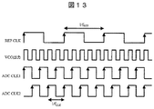
図13に、本実施例に係るタイムインターリーブ型アナログデジタル変換器の動作タイミングを示す。位相同期ループ内の電圧制御発振器(VCO)23の出力は、基準クロック(REF CLK)と同期し、かつ、周波数がN倍のクロックである。Nは分周器24の分周数であり、本図ではN=5である。
FIG. 13 shows the operation timing of the time interleave type analog-digital converter according to this embodiment. The output of the voltage controlled oscillator (VCO) 23 in the phase-locked loop is a clock that is synchronized with the reference clock (REF CLK) and has a frequency N times. N is the frequency dividing number of the
前述したように、第一のアナログデジタル変換部121のサンプリングクロック(ADC CLK1)と、第二のアナログデジタル変換部127のサンプリングクロック(ADC CLK2)は、電圧制御発振器(VCO)23の出力を分周器120で2分周することにより生成される。また、サンプリングクロック(ADC CLK1)とサンプリングクロック(ADC CLK2)の位相は2分の1周期ずれている。
As described above, the sampling clock (ADC CLK1) of the first analog-
これらの波形は、図13に示した通りである。同図に示す通り、第一のサンプリングクロック(ADC CLK1)と第二のサンプリングクロック(ADC CLK2)は、いずれも、基準クロック(REF CLK)と同期し、かつ、立上りタイミング(上向き矢印を付して示す。)の5回に1度、基準クロック(REF CLK)の立上りタイミングと同期する。 These waveforms are as shown in FIG. As shown in the figure, the first sampling clock (ADC CLK1) and the second sampling clock (ADC CLK2) are both synchronized with the reference clock (REF CLK) and rise timing (with an upward arrow). Are synchronized with the rising timing of the reference clock (REF CLK) once every five times.
従って、前述したように、時間デジタル変換器122及び128を用いたジッタの検出が可能である。また、補間器123及び129により、同期タイミングの中間に出現する4つの各サンプリングタイミングにおけるジッタ推定値を補間演算により求めることができる。
Therefore, as described above, it is possible to detect jitter using the time
前述したように、図13では、アナログデジタル変換部の個数Lが2であり、かつ、分周器24の分周数Nが5である場合について、基準クロック(REF CLK)とサンプリングクロック(ADC CLK1及び2)の動作タイミングの関係を説明したが、各数値は他の自然数であっても構わない。ただし、LとNは「互いに素」になるように選定する。この場合、N回に1度ずつ、各サンプリングクロックと基準クロックの立上りタイミングが同期するため、前述した時間デジタル変換器122及び128と同様の補正動作が可能となる。
As described above, in FIG. 13, the reference clock (REF CLK) and the sampling clock (ADC) in the case where the number L of the analog-digital conversion units is 2 and the frequency division number N of the
本実施例の場合も、基準クロック(REF CLK)が十分に低ジッタであることを前提とする。実際、基準クロックとして、一般的な水晶振動子、セラミック振動子、SAW振動子などの発振出力を用いれば、十分に低ジッタの基準クロック(REF CLK)を得ることができる。 Also in the present embodiment, it is assumed that the reference clock (REF CLK) has sufficiently low jitter. Actually, if an oscillation output of a general crystal resonator, ceramic resonator, SAW resonator or the like is used as the reference clock, a sufficiently low jitter reference clock (REF CLK) can be obtained.
(まとめ)
以上説明したように、タイムインターリーブ型アナログデジタル変換器を構成することにより、変換器全体としてのサンプリングクロックが超高速化する場合でも、低消費電力のまま、ジッタの影響をデジタル補正できるアナログデジタル変換器を実現することができる。
(Summary)
As described above, by configuring a time interleaved analog-to-digital converter, analog-to-digital conversion that can digitally correct the effects of jitter while maintaining low power consumption even when the sampling clock of the converter as a whole is extremely fast. Can be realized.
[実施例5]
図14に、第五の実施例に係るアナログデジタル変換器の構成例を示す。本実施例も、タイムインターリーブ型アナログデジタル変換器について説明する。ただし、本実施例に係るアナログデジタル変換器は、各アナログデジタル変換部におけるサンプリングタイミングのスキューをデジタル補正するための機構を有する点において第四の実施例と異なっている。
[Example 5]
FIG. 14 shows a configuration example of the analog-digital converter according to the fifth embodiment. This embodiment also describes a time interleave type analog-digital converter. However, the analog-digital converter according to this embodiment is different from the fourth embodiment in that it has a mechanism for digitally correcting the sampling timing skew in each analog-digital converter.
本実施例の場合も、第四の実施例の場合と同様に、アナログデジタル変換部の個数Lは2であり、第一のアナログデジタル変換部121と第二のアナログデジタル変換部127を備えている。
In the case of the present embodiment as well, as in the case of the fourth embodiment, the number L of analog-digital conversion units is 2, and the first analog-
図12に示す回路構成に加え、本実施例のアナログデジタル変換器は、参照アナログデジタル変換部(ADC0)141と、スキュー探索部142と、加算器143、144を備えている。加算器143は第一のアナログデジタル変換部121用であり、加算器144は第二のアナログデジタル変換部127用である。
In addition to the circuit configuration shown in FIG. 12, the analog-digital converter of the present embodiment includes a reference analog-digital conversion unit (ADC0) 141, a
なお、ジッタの補正に係る部分の回路構成と動作原理は、第四の実施例と同様であるため、本実施例での説明は割愛する。 Note that the circuit configuration and operation principle of the portion relating to the correction of jitter are the same as those in the fourth embodiment, and the description in this embodiment is omitted.
本実施例において、第一のアナログデジタル変換部121のサンプリングクロック(ADC CLK1)と第二のアナログデジタル変換部127のサンプリングクロック(ADC CLK2)のスキュー(ランダムでない一定の時間ずれ)の影響は、以下のようにデジタル補正される。
In the present embodiment, the influence of the skew (a constant non-random time shift) between the sampling clock (ADC CLK1) of the first analog-
参照アナログデジタル変換部141には、2つのアナログデジタル変換部121及び127と同様、入力アナログ電圧が与えられる。すなわち、参照アナログデジタル変換部141は、入力に対し、2つのアナログデジタル変換部121及び127と並列に接続される。
The reference analog-to-
参照アナログデジタル変換部141は、専用のサンプリングクロックにより入力アナログ電圧をサンプリングし、そのサンプリング電圧に対してアナログデジタル変換を実行する。本実施例の場合、参照アナログデジタル変換部用のサンプリングクロックには、位相同期ループ(PLL)20の源振である基準クロック(REF CLK)を使用する。勿論、他のクロックを用いても良い。
The reference analog-to-
スキュー探索部142は、参照アナログデジタル変換部141の出力側に接続される。スキュー探索部142は、参照アナログデジタル変換部141の変換出力、第一のデジタル補正部の出力(図14の「出力1」)、第二のデジタル補正部の出力(図14の「出力2」)等を入力し、第一のサンプリングクロック(ADC CLK1)のスキューと第二のサンプリングクロック(ADC CLK2)のスキューを探索する。各スキューは、参照アナログデジタル変換部用のサンプリングクロックを基準に探索する。この実施例の場合、基準クロック(REF CLK)を基準に探索する。
The
第一のサンプリングクロック(ADC CLK1)と第二のサンプリングクロック(ADC CLK2)のそれぞれについて探索された各スキューの推定値ΔtS1及びΔtS2は、スキュー探索部142から加算器143及び144にそれぞれ出力される。加算器143は、補間器123の出力側に接続され、補間器123から入力されるジッタ推定値とスキュー推定値ΔtS1との加算結果を、乗算器125に出力する。同様に、加算器144は、補間器129の出力側に接続され、補間器129から入力されるジッタ推定値とスキュー推定値ΔtS2との加算結果を、乗算器1211に出力する。
The skew estimated values Δt S1 and Δt S2 searched for the first sampling clock (ADC CLK1) and the second sampling clock (ADC CLK2) are output from the
従って、乗算器125及び1211は、加算器143及び144の出力に、対応する微分器124及び1210の微分出力を乗算した結果を減算器126及び1212に出力する。減算器126及び1212はそれぞれ、アナログデジタル変換部121及び127の生デジタル出力から乗算器125及び1211の出力を減算する。これにより、減算器126及び1212のそれぞれからは、ジッタとスキューによるサンプリング電圧誤差の影響を補正したデジタル値が出力される。
Accordingly, the
なお、図14においては、主要でない結線の一部を省略している。また、スキューの補正に関係するより厳密な構成と動作は、非特許文献3及び4に示されている通りである。 In FIG. 14, some of the non-major connections are omitted. Further, more strict configuration and operation related to skew correction are as shown in Non-Patent Documents 3 and 4.
(まとめ)
以上説明したように、本実施例によれば、サンプリングクロックが超高速化する場合でも、低消費電力のまま、スキューとジッタの影響をデジタル補正できるアナログデジタル変換器を実現することができる。
(Summary)
As described above, according to this embodiment, it is possible to realize an analog-to-digital converter that can digitally correct the effects of skew and jitter while maintaining low power consumption even when the sampling clock is extremely fast.
[実施例6]
図15に、第六の実施例を示す。本実施例は、実施例1で説明したアナログデジタル変換器を、一般の無線送受信機に適用した場合の例である。
[Example 6]
FIG. 15 shows a sixth embodiment. The present embodiment is an example in which the analog-digital converter described in the first embodiment is applied to a general wireless transceiver.
まず、無線受信回路の構成を説明する。アンテナ151で受信された高周波無線信号は、送受切換えスイッチ152を経由し、フロントエンドモジュール(FEM)153に入力される。フロントエンドモジュール153は、フィルタやシングル差動変換用のバラン(平衡不均衡変換器)等で構成される。フロントエンドモジュール153の出力は、RF(Radio Frequency)回路に与えられ信号処理される。RF回路は、例えば低雑音増幅器(LNA)154等で構成される。
First, the configuration of the wireless reception circuit will be described. The high-frequency radio signal received by the
低雑音増幅器154の出力は、受信ミキサ155に与えられ、受信周波数より低周波の信号に周波数変換される。周波数変換された信号は、プリアンプ、可変利得アンプ、フィルタ等から構成されるアナログフロントエンド部(AFE)156により信号処理される。アナログフロントエンド部156の出力信号は、アナログデジタル変換部25等から構成されるアナログデジタル変換器に入力される。
The output of the
アナログデジタル変換器は、受信信号をアナログデジタル変換し、その変換出力をデジタルベースバンド部157に出力する。デジタルベースバンド部157は、妨害波信号のフィルタリングや受信データの復調等を実行し、外部インターフェースに受信データを出力する。
The analog-digital converter converts the received signal from analog to digital and outputs the converted output to the
まず、無線送信回路の構成を説明する。デジタルベースバンド部157は、外部インターフェースから送信データを入力し、当該送信データに基づいて送信ベースバンド信号を生成する。送信ベースバンド信号は、デジタルアナログ変換器158においてアナログ信号に変換される。このアナログ信号はフィルタ159に入力され、送信スペクトルマスクを遵守できるように、帯域制限される。
First, the configuration of the wireless transmission circuit will be described. The
フィルタ159の出力信号は送信ミキサ1510に入力され、高周波信号に周波数変換される。周波数変換後の信号は、パワーアンプ(PA)1511において、所望の送信電力まで電力増幅される。その後、電力増幅後の信号は、送受切換えスイッチ152を経由してアンテナ151に与えられ、送信される。
The output signal of the
受信ミキサ155や送信ミキサ1510は、それぞれの入力信号を、位相同期ループ20から供給される局部発振信号と乗算することにより、所望の周波数変換を実行する。局部発振信号は、基準クロック(REF CLK)を源振とした位相同期ループ20により生成される。
The
この実施例の場合、アナログデジタル変換部25のサンプリングクロック(ADC CLK)は、周波数変換に使用した位相同期ループ20の出力を流用して生成する。このため、位相同期ループ20の出力側に分周器150を接続し、位相同期ループ20の局部発振信号をM分周(Mは整数)してサンプリングクロック(ADC CLK)を生成する。
In the case of this embodiment, the sampling clock (ADC CLK) of the analog-
アナログデジタル変換器を構成するアナログデジタル変換部25、デジタル補正部、時間デジタル変換器26、補間器27の各構成と動作は第一の実施例と同様である。すなわち、アナログデジタル変換器は、時間デジタル変換器26を用いて検出されたジッタ値及びその推定値に基づいてサンプリングクロック(ADC CLK)のジッタの影響をデジタル補正する。
The configurations and operations of the analog-
サンプリングクロック(ADC CLK)と基準クロック(REF CLK)は、周波数が厳密に同期しているため、定期的に両者の立上りタイミングが同期する。従って、第一の実施例と同様の補正動作を実行できる。 Since the sampling clock (ADC CLK) and the reference clock (REF CLK) are strictly synchronized in frequency, the rising timings of both are periodically synchronized. Accordingly, the correction operation similar to that in the first embodiment can be executed.
(まとめ)
以上説明したように、本実施例によれば、超高速のサンプリングクロックで動作するアナログデジタル変換器の無線送受信機への実装が実現される。しかも、本実施例で使用するアナログデジタル変換器は低消費電力である。このため、携帯型の無線送受信機に特に効果的である。
(Summary)
As described above, according to the present embodiment, an analog-digital converter that operates with an ultra-high-speed sampling clock can be mounted on a wireless transceiver. In addition, the analog-digital converter used in this embodiment has low power consumption. For this reason, it is particularly effective for a portable radio transceiver.
[実施例7]
図16に、第七の実施例を示す。本実施例は、実施例1で説明したアナログデジタル変換器を、マイコンチップに適用した場合の例である。
[Example 7]
FIG. 16 shows a seventh embodiment. In this embodiment, the analog-digital converter described in the first embodiment is applied to a microcomputer chip.
マイコンチップは、マイクロプロセッシングユニット(MPU)161やRAM(Random Access Memory)162、ROM(Read Only Memory)163、アナログデジタル変換器、位相同期ループ20等を備えている。
The microcomputer chip includes a microprocessing unit (MPU) 161, a RAM (Random Access Memory) 162, a ROM (Read Only Memory) 163, an analog-digital converter, a phase locked
アナログ入力端子から入力されたアナログ信号は、アナログフロントエンド部156において所要のアナログ信号処理を受ける。この後、アナログ信号は、アナログデジタル変換部25等から構成されるアナログデジタル変換器に入力される。アナログデジタル変換器は、アナログ信号をアナログデジタル変換し、その変換出力をマイクロプロセッシングユニット161に出力する。マイクロプロセッシングユニット161は、処理対象とするアナログ信号について予め定めた処理を実行する。
The analog signal input from the analog input terminal is subjected to required analog signal processing in the analog
マイクロプロセッシングユニット161、RAM162、ROM163の動作に必要な各クロック信号は、位相同期ループ20において生成され、供給される。アナログデジタル変換部25のサンプリングクロック(ADC CLK)も、位相同期ループ20の出力を流用して生成される。具体的には、位相同期ループ20の局部発振信号を分周器150に与えてM分周(Mは整数)し、サンプリングクロック(ADC CLK)を生成する。
Each clock signal necessary for the operation of the
アナログデジタル変換部25、デジタル補正部、時間デジタル変換器26、補間器27の構成と動作は第一の実施例と同様である。すなわち、アナログデジタル変換器は、時間デジタル変換器26を用いて検出されたジッタ値及びその推定値に基づいてサンプリングクロック(ADC CLK)のジッタの影響をデジタル補正する。
The configurations and operations of the analog-
サンプリングクロック(ADC CLK)と基準クロック(REF CLK)は、周波数が厳密に同期しているため、定期的に両者の立上りタイミングが同期する。従って、第一の実施例と同様の補正動作を実行できる。 Since the sampling clock (ADC CLK) and the reference clock (REF CLK) are strictly synchronized in frequency, the rising timings of both are periodically synchronized. Accordingly, the correction operation similar to that in the first embodiment can be executed.
(まとめ)
以上説明したように、本実施例によれば、超高速のサンプリングクロックで動作するアナログデジタル変換器のマイコンチップへの実装が実現される。しかも、本実施例で使用するアナログデジタル変換器は低消費電力である。このため、携帯機器に搭載されるマイコンチップに特に効果的である。
(Summary)
As described above, according to this embodiment, the analog-digital converter that operates with the ultra-high-speed sampling clock can be mounted on the microcomputer chip. In addition, the analog-digital converter used in this embodiment has low power consumption. For this reason, it is particularly effective for a microcomputer chip mounted on a portable device.
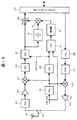
[時間デジタル変換器の具体例]
図17に、各実施例で使用する時間デジタル変換器(TDC)の回路実装例を示す。すなわち、時間デジタル変換器26(図2、図8、図10、図15、図16)や時間デジタル変換器122、128(図12、図14)に用いて好適な回路実装例を示す。
[Specific examples of time digital converters]
FIG. 17 shows a circuit implementation example of a time digital converter (TDC) used in each embodiment. That is, a circuit implementation example suitable for the time digital converter 26 (FIGS. 2, 8, 10, 15, and 16) and the time
「IN1」からADC CLKが、「IN2」からREF CLKが入力される。これら2つのクロック入力は位相周波数比較器171に入力される。位相周波数比較器171は、2つのクロックの立上りタイミングに応じて、チャージポンプ172を制御する。その制御に応じてチャージポンプ172の出力から容量素子CINT173に対して電流が充放電される。その結果、チャージポンプ172の出力には、ADC CLKとREF CLKの立上りタイミングの時間差に応じた電圧が生じる。この電圧は、抵抗ラダー176、コンパレータ列177、温度計コードTOバイナリコード変換部178からなる従来のフラッシュADC(Analog to Digital Conveter)構成により、デジタル値にA/D変換される。以上の通り、2つの入力CLKの立上りタイミング時間差に応じたデジタル値が出力「OUT」に得られる。
ADC CLK from the "IN 1" is, REF CLK from the "IN 2" is input. These two clock inputs are input to the phase frequency comparator 171. The phase frequency comparator 171 controls the charge pump 172 according to the rising timings of the two clocks. In accordance with the control, current is charged and discharged from the output of the charge pump 172 to the
以下、時間デジタル変換器を構成する各部の構成と動作を詳細に説明する。位相周波数比較器171は、従来のPLLでしばしば用いられる位相周波数比較器と同じ構成でよい。すなわち、2つのDフリップフロップ171A、171Bは、クロック入力端子「CK」がそれぞれIN1(ADC CLK)とIN2(REF CLK)に接続され、データ入力端子「D」が電源電圧VDDに接続される。また、遅延ANDゲート171Cの入力には、これら2つのDフリップフロップの出力が接続される。また、遅延ANDゲート171Cの出力は、2つのDフリップフロップ171A、171Bのリセット端子「Reset」に接続される。
Hereinafter, the configuration and operation of each unit constituting the time digital converter will be described in detail. The phase frequency comparator 171 may have the same configuration as the phase frequency comparator often used in the conventional PLL. That is, in the two D flip-
図18に、TDCを構成する各部の動作波形を示す。図18に示すように、Dフリップフロップ171Aの出力(図17の「VA」)は、ADC CLKの立上りタイミングに同期して、出力がローレベルからハイレベルに変化する。一方、Dフリップフロップ171Bの出力(図17の「VB」)は、REF CLKの立上りタイミングに同期して、出力がローレベルからハイレベルに変化する。
FIG. 18 shows operation waveforms of respective parts constituting the TDC. As shown in FIG. 18, the output of the D flip-
2つのDフリップフロップ171A、171Bの出力がともにハイレベルになると、遅延ANDゲート171Cの出力は、意図的に設定したTOVの遅延時間の後、ローレベルからハイレベルに変化する。その結果、2つのDフリップフロップ171A、171Bの各出力がローレベルにリセットされる。すなわち、図18に示す通り、出力VA、VBは、ADC CLKとREF CLKのいずれか立上りタイミングの遅い方の立上りタイミングから更にTOVの時間だけ経過した後、ともに出力がローレベルになる。なお、前述したように意図的なTOV期間を設けるのは、ADC CLKとREF CLKの立上りタイミングの時間差が極めて小さい時にも、CLKを正しく検出できるようにするためである。この技術は、PLLの位相周波数比較器171の「デッドゾーン」回避技術として一般的に知られている。
When the outputs of the two D flip-
まず、ADC CLKの立上がりタイミングの方が、REF CLKの立上りタイミングよりも早い場合(図18の「ケース1」)について説明する。ADC CLKの立上りタイミングにおいて、Dフリップフロップ171Aの出力VAがハイレベルになると、反転ゲート171Dの出力がローレベルになる。この場合、チャージポンプ172内のPMOSスイッチ172Aがオンになる。その結果、PMOS電流源172CよりPMOSスイッチ172Aを経由して、容量素子CINT173に電流が充電される。この充電の間、チャージポンプ172の出力電圧VCは直線的に増加する。
First, the case where the rising timing of ADC CLK is earlier than the rising timing of REF CLK (“
その後、REF CLKの立上りタイミングにおいて、Dフリップフロップ171Bの出力VBもハイレベルになると、NMOSスイッチ172Bもオンになる。この場合、NMOSスイッチ172Bを経由して、容量素子CINT173からNMOS電流源172Dに電流が吸い出される。ここで、PMOS電流源172Cによる供給電流値とNMOS電流源172Dによる吸い込み電流値は、同一値に設定されている。そのため、供給電流と吸い込み電流が相殺され、容量素子CINT173には電流が流れなくなる。その結果、REF CLKの立上りタイミング以降、チャージポンプ172の出力電圧VCは一定に保持される。すなわち、容量素子CINT173には、ADC CLKとREF CLKの立上りタイミング時間差に相当する期間だけ電流が充電され、充電後の電圧値がそのまま保持される。
Thereafter, when the output V B of the D flip-flop 171B becomes high level at the rising timing of REF CLK, the
次に、REF CLKの立上がりタイミングの方が、ADC CLKの立上りタイミングより早い場合(図18「ケース2」)について説明する。この場合、Dフリップフロップ171Bの出力VBが、Dフリップフロップ171Aの出力VAよりも先にオンになる。このため、REF CLKとADC CLKの立上りタイミング時間差に相当する期間だけ容量素子CINT173から電流が放電され、放電後の電圧値がそのまま保持される。
以上から、チャージポンプ172の出力電圧VCは、次式となる。
Next, the case where the rising timing of REF CLK is earlier than the rising timing of ADC CLK (“
From the above, the output voltage V C of the charge pump 172 is expressed by the following equation.

ここで、ICPはPMOS電流源172CとNMOS電流源172Dの電流値、Δtは、ADC CLKとREF CLKの立上りタイミング時間差(ADC CLKのほうが立上りタイミングが早い場合を正符号に定義)である。また、図17に示す通り、容量素子CINT173の下部電極を電圧源175に接続することで、出力電圧VCに直流バイアスを与えている。本例では、後段に位置するフラッシュADC部の動作に都合のよいVDD/2を直流バイアスとして与える。このため、電圧源175の電圧値はVDD/2に設定している。
Here, I CP is a current value of the PMOS
フラッシュADC部では、チャージポンプ172の出力電圧VCをmビットでA/D変換する。フラッシュADC部のコンパレータ列177を構成する各コンパレータ(図中、三角形の記号で示す)は、クロック生成部179(CLKGEN)がREF CLKから生成するCMPCLKの立上りタイミングをトリガに用い、出力電圧VCと、抵抗ラダー176から供給される各比較用電圧とを比較する。各コンパレータは、その比較結果に応じてハイレベルかローレベルのいずれかを出力する。
The flash ADC unit, the output voltage V C of the charge pump 172 to A / D conversion in m bits. Each comparator (indicated by a triangular symbol in the figure) constituting the
温度計コードTOバイナリコード変換部178は、各コンパレータの出力をバイナリコードに変換して「OUT」として出力する。ここで、容量素子CINT173に保持された電荷は、チャージポンプ172内のPMOSスイッチ172AとNMOSスイッチ172Bや、容量素子CINT173に対して並列に接続されたリセットスイッチ174などを経由してリークする恐れがある。そのため、リーク期間(出力電圧VCが確定してから各コンパレータが判定を開始するまでの期間(図18のTAD))を、必要最小限に留めるべきである。
The thermometer code TO binary
フラッシュADC部におけるA/D変換が完了した後(すなわち、図18における「OUT」の確定後)、RSTCLKをハイレベルに立上げてリセットスイッチ174をオンにする。これにより、容量素子CINT173の電荷はゼロにリセットされる。すなわち、容量素子CINT173は、ADC CLKの立上がりタイミングとREF CLKの立上がりタイミングの次回の比較に備える状態になる。RSTCLKもCMPCLKと同様にクロック生成部179において、REF CLKから生成することができる。
After the A / D conversion in the flash ADC unit is completed (that is, after “OUT” in FIG. 18 is determined), RSTCLK is raised to a high level and the
なお、式(1)が示す通り、図17に示すTDCの変換利得は、ICP/CINTで与えられる。この変換利得を高めることにより、フラッシュADC部で発生する雑音電圧は、TDCの入力換算ジッタとしては十分に小さくすることができる。また、2つのDフリップフロップ171Aと171Bの入力換算ジッタは、そのままTDCの入力換算ジッタになる。このため、2つのDフリップフロップ171Aと171Bの入力換算ジッタは十分に低減する必要がある。TDCの入力換算ジッタの低減は、各実施例に適用するTDCとして最も要求される性能である。
As shown in equation (1), the conversion gain of TDC shown in FIG. 17 is given by I CP / C INT . By increasing the conversion gain, the noise voltage generated in the flash ADC unit can be sufficiently reduced as the input conversion jitter of the TDC. The input conversion jitter of the two D flip-
例えば最大±8psのジッタを想定し、4ビットのTDCにより変換する場合、1LSBは、8ps×2/24=1psである。このTDCを用いて各実施例の補正を行うことにより、補正後の残留ジッタを±1/2 LSB以下(すなわち、±0.5ps以下)に低減することができる。上記の通り、ADC CLKとREF CLKの立上りタイミング時間差は、変換利得ICP/CINTにより電圧に変換される。例えば、ICP=2mA、CINT=50fFの場合、1psの時間差は40mVの電圧に変換される。従って、フラッシュADC部は、1LSBが40mVで、フルスケール電圧は、40mV×24=640mVで設計する。 For example, assuming a maximum jitter of ± 8 ps and converting by 4-bit TDC, 1 LSB is 8 ps × 2/2 4 = 1 ps. By performing correction of each embodiment using this TDC, the corrected residual jitter can be reduced to ± 1/2 LSB or less (that is, ± 0.5 ps or less). As described above, the rise timing time difference between ADC CLK and REF CLK is converted into a voltage by the conversion gain I CP / C INT . For example, when I CP = 2 mA and C INT = 50 fF, a time difference of 1 ps is converted into a voltage of 40 mV. Therefore, the flash ADC unit is designed so that 1 LSB is 40 mV and the full-scale voltage is 40 mV × 2 4 = 640 mV.
なお、反転ゲート171Dやチャージポンプ172内のPMOSスイッチ172A、NMOSスイッチ172Bなどの応答遅延により生じる可能性のあるTDCの入力換算直流オフセットは、容易に検出して除去することが可能である。このため、入力換算直流オフセットは問題にならないと考えられる。
It is possible to easily detect and remove the TDC input-converted DC offset that may be caused by response delays of the inverting
10:アナログデジタル変換器
11:位相同期ループ
12:分周器
13:アナログデジタル変換部
14:時間デジタル変換器
15:デジタル補正部
20:位相同期ループ
21:位相比較器
22:ループフィルタ
23:電圧制御発振器
24:分周器
25:アナログデジタル変換部
26:TDC(時間デジタル変換器)
27:補間器
28:微分器
29:乗算器
210:減算器
61〜65:遅延器
66〜611:定数倍器
612:加算器
71:遅延器
72:加算器
81:デューティ調整部
82:バンドパスフィルタ
83:バッファ
101:注入同期型発振器
120:1/2分周器
121、127:アナログデジタル変換部
122、128:TDC
123、129:補間器
124、1210:微分器
125、1211:乗算器
126、1212:減算器
141:参照アナログデジタル変換部
142:スキュー探索部
143、144:加算器
150:分周器
151:アンテナ
152:スイッチ
153:フロントエンドモジュール
154:低雑音増幅器
155:受信ミキサ
156:アナログフロントエンド部
157:デジタルベースバンド部
158:デジタルアナログ変換器
159:フィルタ
1510:送信ミキサ
1511:パワーアンプ
161:MPU(マイクロプロセッシングユニット)
162:RAM(ランダムアクセスメモリ)
163:ROM(リードオンリーメモリ)
171:位相周波数比較器
171A、171B:Dフリップフロップ
171C:遅延AND(アンド)ゲート
171D:反転(インバータ)ゲート
172:チャージポンプ
172A:PMOSスイッチ
172B:NMOSスイッチ
172C:PMOS電流源
172D:NMOS電流源
173:容量素子
174:リセットスイッチ
175:電圧源
176:抵抗ラダー
177:コンパレータ列
178:温度計コードTOバイナリコード変換部
179:クロック生成部
10: analog-digital converter 11: phase-locked loop 12: frequency divider 13: analog-digital converter 14: time digital converter 15: digital correction unit 20: phase-locked loop 21: phase comparator 22: loop filter 23: voltage Control oscillator 24: Frequency divider 25: Analog-digital converter 26: TDC (time digital converter)
27: Interpolator 28: Differentiator 29: Multiplier 210: Subtractors 61-65: Delayers 66-611: Constant multiplier 612: Adder 71: Delayer 72: Adder 81: Duty adjuster 82: Band pass Filter 83: Buffer 101: Injection locked oscillator 120: 1/2
123, 129:
162: RAM (random access memory)
163: ROM (Read Only Memory)
171:
Claims (15)
基準クロックを源振とし、前記基準クロックより高周波数であり、かつ、前記基準クロックと同期したサンプリングクロックを生成する位相同期ループと、
前記入力アナログ電圧を前記サンプリングクロックを用いてサンプリングし、デジタル値に変換するアナログデジタル変換部と、
前記基準クロックの電圧遷移タイミングに対する前記サンプリングクロックの時間遷移タイミングの時間差を検出し、前記時間差を差分デジタル値に変換する時間デジタル変換器と、
前記差分デジタル値を補間して各サンプリングタイミングに対応する補間値を求め、前記補間値により前記アナログデジタル変換部の生デジタル出力に含まれる前記サンプリングクロックのジッタの影響をデジタル補正するデジタル補正部と
を有することを特徴とするアナログデジタル変換器。 In the analog-digital converter that samples the input analog voltage and converts it to a digital value,
A phase-locked loop that generates a sampling clock having a reference clock as a source and having a higher frequency than the reference clock and synchronized with the reference clock;
The input analog voltage is sampled using the sampling clock, and converted to a digital value, an analog-to-digital converter,
A time digital converter that detects a time difference of a time transition timing of the sampling clock with respect to a voltage transition timing of the reference clock, and converts the time difference into a differential digital value;
A digital correction unit that interpolates the difference digital value to obtain an interpolation value corresponding to each sampling timing, and digitally corrects the influence of jitter of the sampling clock included in the raw digital output of the analog-to-digital conversion unit by the interpolation value; An analog-to-digital converter characterized by comprising:
前記デジタル補正部は、前記アナログデジタル変換部の生デジタル出力の微分値を求め、前記微分値と前記補間値に基づいて前記生デジタル出力をデジタル補正する
ことを特徴とするアナログデジタル変換器。 The analog-digital converter according to claim 1,
The analog-to-digital converter, wherein the digital correction unit obtains a differential value of the raw digital output of the analog-digital conversion unit and digitally corrects the raw digital output based on the differential value and the interpolated value.
それぞれが、対応する第1のサンプリングクロックを用いて前記入力アナログ電圧をサンプリングし、デジタル値に変換する複数のアナログデジタル変換部であって、複数の前記第1のサンプリングクロックは、周波数が互いに同一であり、かつ、位相が互いに異なる関係を有する、複数のアナログデジタル変換部と、
各アナログデジタル変換部に対応して設けられ、それぞれが、基準クロックの電圧遷移タイミングに対する前記第1のサンプリングクロックの時間遷移タイミングの時間差を検出し、前記時間差を差分デジタル値に変換する複数の時間デジタル変換器であり、前記第1のサンプリングクロックの周波数は、位相同期ループ用である前記基準クロックの周波数より低周波数である、複数の時間デジタル変換器と、
各アナログデジタル変換部に対応して設けられ、それぞれが、前記差分デジタル値を補間して各サンプリングタイミングに対応する補間値を求め、前記補間値により対応する前記アナログデジタル変換部の生デジタル出力に含まれる前記第1のサンプリングクロックのジッタの影響をデジタル補正する複数のデジタル補正部と
を有することを特徴とするアナログデジタル変換器。 In the analog-digital converter that samples the input analog voltage and converts it to a digital value,
Each of the plurality of analog-to-digital converters samples the input analog voltage using a corresponding first sampling clock and converts it into a digital value, and the plurality of first sampling clocks have the same frequency. And a plurality of analog-digital converters having different relationships in phase, and
A plurality of times provided corresponding to each analog-to-digital converter, each detecting a time difference of the time transition timing of the first sampling clock with respect to the voltage transition timing of the reference clock, and converting the time difference into a differential digital value A plurality of time digital converters, wherein the frequency of the first sampling clock is lower than the frequency of the reference clock for a phase locked loop ;
Provided corresponding to each analog-to-digital conversion unit, each interpolates the difference digital value to obtain an interpolation value corresponding to each sampling timing, and to the raw digital output of the corresponding analog-to-digital conversion unit by the interpolation value An analog-to-digital converter, comprising: a plurality of digital correction units that digitally correct the influence of jitter of the first sampling clock included.
参照アナログデジタル変換器と
スキュー探索部とを有し、
前記参照アナログデジタル変換器は、各アナログデジタル変換部に対応する複数の第1のサンプリングクロックとサンプリングタイミングを順次同期できる周波数の第2のサンプリングクロックにより前記入力アナログ電圧をサンプリングして参照用デジタル値を生成し、
前記スキュー探索部は、前記参照用デジタル値を用いて、複数の前記第1のサンプリングクロックにそれぞれ含まれるサンプリングタイミングスキューを探索し、得られたサンプリングタイミングスキューをそれぞれ対応する前記デジタル補正部に与え、
前記複数のデジタル補正部は、それぞれが、対応する前記補間値と前記サンプリングタイミングスキューとに基づいて、対応する前記アナログデジタル変換部の生デジタル出力に含まれる前記第1のサンプリングクロックのジッタとスキューの影響をデジタル補正する
ことを特徴とするアナログデジタル変換器。 The analog-digital converter according to claim 3,
A reference analog-to-digital converter and a skew search unit,
The reference analog-to-digital converter samples the input analog voltage with a second sampling clock having a frequency that can sequentially synchronize the sampling timing with a plurality of first sampling clocks corresponding to each analog-to-digital converter, and a reference digital value Produces
The skew search unit searches the sampling timing skew included in each of the plurality of first sampling clocks using the reference digital value, and gives the obtained sampling timing skew to the corresponding digital correction unit. ,
Each of the plurality of digital correction units includes a jitter and a skew of the first sampling clock included in the raw digital output of the corresponding analog-to-digital conversion unit based on the corresponding interpolation value and the sampling timing skew. An analog-to-digital converter characterized by digitally correcting the effects of
複数の前記第1のサンプリングクロックは、前記第1のサンプリングクロックよりも低周波数である基準クロックを源振とする位相同期ループにより生成される前記基準クロックと同期した第3のサンプリングクロックを分周することにより生成する
ことを特徴とするアナログデジタル変換器。 The analog-digital converter according to claim 3,
The plurality of first sampling clocks divide a third sampling clock synchronized with the reference clock generated by a phase-locked loop that uses a reference clock having a lower frequency than the first sampling clock as a source. An analog-to-digital converter characterized by being generated by
複数の前記第1のサンプリングクロックは、前記第1のサンプリングクロックよりも低周波数である基準クロックを源振とする位相同期ループにより生成される前記基準クロックと同期した第4のサンプリングクロックを分周することにより生成する
ことを特徴とするアナログデジタル変換器。 The analog-digital converter according to claim 4,
The plurality of first sampling clocks divide a fourth sampling clock synchronized with the reference clock generated by a phase-locked loop using a reference clock having a frequency lower than that of the first sampling clock as a source. An analog-to-digital converter characterized by being generated by
複数の前記デジタル補正部のそれぞれは、対応する前記アナログデジタル変換部の生デジタル出力の微分値を求め、前記微分値と対応する前記補間値に基づいて前記生デジタル出力をデジタル補正する
ことを特徴とするアナログデジタル変換器。 The analog-digital converter according to claim 3,
Each of the plurality of digital correction units obtains a differential value of the raw digital output of the corresponding analog-digital conversion unit, and digitally corrects the raw digital output based on the interpolation value corresponding to the differential value. Analog to digital converter.
複数の前記デジタル補正部のそれぞれは、対応する前記アナログデジタル変換部の生デジタル出力の微分値を求め、前記微分値と対応する前記補間値に基づいて前記生デジタル出力をデジタル補正する
ことを特徴とするアナログデジタル変換器。 The analog-digital converter according to claim 4,
Each of the plurality of digital correction units obtains a differential value of the raw digital output of the corresponding analog-digital conversion unit, and digitally corrects the raw digital output based on the interpolation value corresponding to the differential value. Analog to digital converter.
複数の前記デジタル補正部のそれぞれは、対応する前記アナログデジタル変換部の生デジタル出力の微分値を求め、前記微分値と対応する前記補間値に基づいて前記生デジタル出力をデジタル補正する
ことを特徴とするアナログデジタル変換器。 The analog-digital converter according to claim 5,
Each of the plurality of digital correction units obtains a differential value of the raw digital output of the corresponding analog-digital conversion unit, and digitally corrects the raw digital output based on the interpolation value corresponding to the differential value. Analog to digital converter.
複数の前記デジタル補正部のそれぞれは、対応する前記アナログデジタル変換部の生デジタル出力の微分値を求め、前記微分値と対応する前記補間値に基づいて前記生デジタル出力をデジタル補正する
ことを特徴とするアナログデジタル変換器。 The analog-digital converter according to claim 6,
Each of the plurality of digital correction units obtains a differential value of the raw digital output of the corresponding analog-digital conversion unit, and digitally corrects the raw digital output based on the interpolation value corresponding to the differential value. Analog to digital converter.
前記基準クロック又はその分周出力に含まれる高調波をフィルタにより抽出し、さらに、抽出された前記高調波を分周することにより、複数の各アナログデジタル変換部に対応する前記第1のサンプリングクロックを生成する
ことを特徴とするアナログデジタル変換器。 The analog-digital converter according to claim 3,
The first sampling clock corresponding to each of the plurality of analog-digital converters is extracted by extracting the harmonics included in the reference clock or the frequency-divided output by a filter, and further dividing the extracted harmonics. An analog-to-digital converter characterized by generating
前記基準クロック又はその分周出力に含まれる高調波をフィルタにより抽出し、さらに、抽出された前記高調波を分周することにより、複数の各アナログデジタル変換部に対応する前記第1のサンプリングクロックを生成する
ことを特徴とするアナログデジタル変換器。 The analog-digital converter according to claim 4,
The first sampling clock corresponding to each of the plurality of analog-digital converters is extracted by extracting the harmonics included in the reference clock or the frequency-divided output by a filter, and further dividing the extracted harmonics. An analog-to-digital converter characterized by generating
前記基準クロック又はその分周出力を注入同期型発振器に注入し、前記注入同期型発振器の発振出力を分周し、得られた分周出力を用いて、複数の前記アナログデジタル変換部のそれぞれに対応する複数の前記第1のサンプリングクロックを生成する
ことを特徴とするアナログデジタル変換器。 The analog-digital converter according to claim 3,
Injecting the reference clock or the divided output thereof into an injection-locked oscillator, dividing the oscillation output of the injection-locked oscillator, and using the obtained divided output, each of the plurality of analog-digital converters A plurality of corresponding first sampling clocks are generated. An analog-to-digital converter, characterized in that:
前記基準クロック又はその分周出力を注入同期型発振器に注入し、前記注入同期型発振器の発振出力を分周し、得られた分周出力を用いて、複数の前記アナログデジタル変換部のそれぞれに対応する複数の前記第1のサンプリングクロックを生成する
ことを特徴とするアナログデジタル変換器。 The analog-digital converter according to claim 4,
Injecting the reference clock or the divided output thereof into an injection-locked oscillator, dividing the oscillation output of the injection-locked oscillator, and using the obtained divided output, each of the plurality of analog-digital converters A plurality of corresponding first sampling clocks are generated. An analog-to-digital converter, characterized in that:
基準クロックを源振とし、前記基準クロックより高周波数であり、かつ、前記基準クロックと同期したサンプリングクロックを生成する位相同期ループと、
前記入力アナログ電圧を前記サンプリングクロックを用いてサンプリングし、デジタル値に変換するアナログデジタル変換部と、
前記基準クロックの電圧遷移タイミングに対する前記サンプリングクロックの時間遷移タイミングの時間差を検出し、前記時間差を差分デジタル値に変換する時間デジタル変換器と、
前記差分デジタル値を補間して各サンプリングタイミングに対応する補間値を求め、前記補間値により前記アナログデジタル変換部の生デジタル出力に含まれる前記サンプリングクロックのジッタの影響をデジタル補正するデジタル補正部と
を有するアナログデジタル変換器を有する受信回路部と、
前記無線信号を周波数変換するための局部発振信号を生成する位相同期ループと
を有することを特徴とする無線受信機。 A receiving circuit unit for receiving a radio signal,
A phase-locked loop that generates a sampling clock having a reference clock as a source and having a higher frequency than the reference clock and synchronized with the reference clock;
The input analog voltage is sampled using the sampling clock, and converted to a digital value, an analog-to-digital converter,
A time digital converter that detects a time difference of a time transition timing of the sampling clock with respect to a voltage transition timing of the reference clock, and converts the time difference into a differential digital value;
A digital correction unit that interpolates the difference digital value to obtain an interpolation value corresponding to each sampling timing, and digitally corrects the influence of jitter of the sampling clock included in the raw digital output of the analog-to-digital conversion unit by the interpolation value; A receiving circuit unit having an analog-digital converter having
And a phase-locked loop for generating a local oscillation signal for frequency-converting the radio signal.
Priority Applications (2)
| Application Number | Priority Date | Filing Date | Title |
|---|---|---|---|
| JP2011193965A JP5684076B2 (en) | 2011-09-06 | 2011-09-06 | Analog to digital converter and radio receiver |
| US13/570,228 US8933831B2 (en) | 2011-09-06 | 2012-08-08 | Analog-to-digital converter and wireless receiver |
Applications Claiming Priority (1)
| Application Number | Priority Date | Filing Date | Title |
|---|---|---|---|
| JP2011193965A JP5684076B2 (en) | 2011-09-06 | 2011-09-06 | Analog to digital converter and radio receiver |
Publications (2)
| Publication Number | Publication Date |
|---|---|
| JP2013055598A JP2013055598A (en) | 2013-03-21 |
| JP5684076B2 true JP5684076B2 (en) | 2015-03-11 |
Family
ID=47753175
Family Applications (1)
| Application Number | Title | Priority Date | Filing Date |
|---|---|---|---|
| JP2011193965A Expired - Fee Related JP5684076B2 (en) | 2011-09-06 | 2011-09-06 | Analog to digital converter and radio receiver |
Country Status (2)
| Country | Link |
|---|---|
| US (1) | US8933831B2 (en) |
| JP (1) | JP5684076B2 (en) |
Cited By (1)
| Publication number | Priority date | Publication date | Assignee | Title |
|---|---|---|---|---|
| KR20190143028A (en) * | 2018-06-19 | 2019-12-30 | 세종대학교산학협력단 | Time digital converting counter and lidar system comprising the same |
Families Citing this family (37)
| Publication number | Priority date | Publication date | Assignee | Title |
|---|---|---|---|---|
| US8461886B1 (en) * | 2010-10-20 | 2013-06-11 | Marvell International Ltd. | Circuit and circuit method for reduction of PFD noise contribution for ADPLL |
| JP6192259B2 (en) * | 2011-04-21 | 2017-09-06 | 三星電子株式会社Samsung Electronics Co.,Ltd. | DTV analog front end, digital TV system including the same, and methods of operation thereof |
| US8669794B2 (en) * | 2012-02-21 | 2014-03-11 | Qualcomm Incorporated | Circuit for detecting a voltage change using a time-to-digital converter |
| US8922184B2 (en) * | 2012-03-22 | 2014-12-30 | Realtek Semiconductor Corp. | Integrated switch-capacitor DC-DC converter and method thereof |
| US8830106B2 (en) * | 2012-08-30 | 2014-09-09 | Texas Instruments Incorporated | Asynchronous analog-to-digital converter having adapative reference control |
| US8754797B2 (en) * | 2012-08-30 | 2014-06-17 | Texas Instruments Incorporated | Asynchronous analog-to-digital converter having rate control |
| US8878577B2 (en) * | 2012-09-05 | 2014-11-04 | IQ-Analog Corporation | System and method for frequency multiplier jitter correction |
| US8994423B2 (en) * | 2013-01-29 | 2015-03-31 | Perceptia Devices Australia, Pty Ltd. | Phase-locked loop apparatus and method |
| JP6273931B2 (en) * | 2014-03-14 | 2018-02-07 | シンフォニアテクノロジー株式会社 | Signal converter for power converter |
| KR101624507B1 (en) | 2014-04-03 | 2016-05-26 | 한국과학기술원 | Clock signal processor, receiver and transmitting/receiving system |
| KR101615435B1 (en) * | 2014-06-09 | 2016-04-26 | 한국과학기술원 | An appratus for sensing temperature using a sensor resistor and a method thereof |
| US9651646B2 (en) * | 2014-06-24 | 2017-05-16 | Tektronix, Inc. | Phase noise correction system for discrete time signal processing |
| WO2016081046A2 (en) * | 2014-09-03 | 2016-05-26 | University Of Southern California | Wideband nyquist vco-based analog-to-digital converter |
| US9231602B1 (en) * | 2014-09-18 | 2016-01-05 | Intel IP Corporation | A-priori-probability-phase-estimation for digital phase-locked loops |
| JP6416607B2 (en) * | 2014-12-10 | 2018-10-31 | 日立オートモティブシステムズ株式会社 | Electronic control unit |
| US9379880B1 (en) * | 2015-07-09 | 2016-06-28 | Xilinx, Inc. | Clock recovery circuit |
| JP6694728B2 (en) * | 2016-02-18 | 2020-05-20 | 日本電波工業株式会社 | Signal processor |
| US9588497B1 (en) * | 2016-07-27 | 2017-03-07 | Silicon Laboratories Inc. | Differential voltage-controlled oscillator analog-to-digital converter using input-referred offset |
| US10454483B2 (en) * | 2016-10-24 | 2019-10-22 | Analog Devices, Inc. | Open loop oscillator time-to-digital conversion |
| US9991898B1 (en) * | 2016-11-16 | 2018-06-05 | Perceptia Devices, Inc. | Fractional-N jitter attenuator |
| US10044383B2 (en) | 2016-12-30 | 2018-08-07 | Silicon Laboratories Inc. | Sinewave generation from multi-phase signals |
| US9979404B1 (en) | 2016-12-30 | 2018-05-22 | Silicon Laboratories Inc. | Multi-phase amplitude and phase modulation |
| EP3442129B1 (en) * | 2017-08-11 | 2020-06-03 | Samsung Electronics Co., Ltd. | Receiver and reception method based on pulse |
| KR102370285B1 (en) * | 2017-08-11 | 2022-03-07 | 삼성전자주식회사 | Receiver and receiving method based on pulse |
| KR102452620B1 (en) * | 2017-09-29 | 2022-10-07 | 삼성전자주식회사 | Apparatus and method for detecting touch |
| US10291247B1 (en) * | 2018-03-07 | 2019-05-14 | Xilinx, Inc. | Chopping switch time-skew calibration in time-interleaved analog-to-digital converters |
| US10483996B1 (en) * | 2018-05-29 | 2019-11-19 | Xilinx, Inc. | Time skew calibration of time-interleaved analog to digital converters |
| US10509104B1 (en) * | 2018-08-13 | 2019-12-17 | Analog Devices Global Unlimited Company | Apparatus and methods for synchronization of radar chips |
| US11231741B1 (en) * | 2018-10-11 | 2022-01-25 | Marvell Asia Pte, Ltd. | Systems and methods for generating clock signals |
| CN110069008B (en) * | 2019-04-29 | 2020-05-22 | 复旦大学 | Time-to-digital converter system and multiple delay phase-locked loop comprising same |
| CN110212912B (en) * | 2019-06-06 | 2020-07-03 | 复旦大学 | Multiple delay phase-locked loop with high-precision time-to-digital converter |
| US11283437B2 (en) * | 2019-12-17 | 2022-03-22 | Skyworks Solutions, Inc. | Measuring pin-to-pin delays between clock routes |
| US10958257B1 (en) * | 2020-04-28 | 2021-03-23 | Taiwan Semiconductor Manufacturing Company Limited | System and method for adjusting duty cycle of a signal |
| EP3996280A1 (en) * | 2020-11-05 | 2022-05-11 | Stichting IMEC Nederland | Circuit and method for random edge injection locking |
| CN112698363B (en) * | 2020-12-29 | 2024-04-16 | 成都国星通信有限公司 | High-precision data acquisition method and acquisition circuit for Beidou anti-interference antenna |
| JP2022146460A (en) * | 2021-03-22 | 2022-10-05 | キオクシア株式会社 | Semiconductor circuit, reception device, and memory system |
| CN116015287B (en) * | 2022-12-31 | 2024-03-19 | 成都电科星拓科技有限公司 | Method and device for correcting TDC stepping based on frequency-to-voltage circuit |
Family Cites Families (13)
| Publication number | Priority date | Publication date | Assignee | Title |
|---|---|---|---|---|
| DE10007408A1 (en) * | 2000-02-18 | 2001-09-06 | Infineon Technologies Ag | Analog-to-digital converter circuit arrangement - includes control device for supplying a given input signal value for calibration purposes and for evaluating the resultant digital output signal value of converter |
| JP2003133954A (en) | 2001-10-26 | 2003-05-09 | Agilent Technologies Japan Ltd | Calibration method for interleave system a/d converter |
| JP3692405B2 (en) * | 2003-04-18 | 2005-09-07 | 独立行政法人情報通信研究機構 | Analog / digital converter performance measurement system and performance measurement method, and digital / analog converter performance measurement system and performance measurement method |
| US7248194B2 (en) * | 2003-06-04 | 2007-07-24 | Koninklijke Philips Electronics N.V. | Bit-detection arrangement and apparatus for reproducing information |
| US7332973B2 (en) * | 2005-11-02 | 2008-02-19 | Skyworks Solutions, Inc. | Circuit and method for digital phase-frequency error detection |
| US7365607B2 (en) * | 2006-08-10 | 2008-04-29 | Newport Media, Inc. | Low-power, low-jitter, fractional-N all-digital phase-locked loop (PLL) |
| CN101632229A (en) * | 2007-02-28 | 2010-01-20 | 松下电器产业株式会社 | A/D converter and A/D converting method |
| JP4271244B2 (en) * | 2007-03-26 | 2009-06-03 | 株式会社半導体理工学研究センター | Analog-digital (AD) converter and analog-digital conversion method |
| CA2688528C (en) * | 2007-06-21 | 2015-04-14 | Signal Processing Devices Sweden Ab | Compensation of mismatch errors in a time-interleaved analog-to-digital converter |
| JP4977570B2 (en) * | 2007-10-03 | 2012-07-18 | 株式会社日立製作所 | DIGITAL CALIBRATION TYPE ANALOG / DIGITAL CONVERTER AND RADIO RECEIVING CIRCUIT AND RADIO TRANSMITTING / RECEIVER CIRCUIT USING THE SAME |
| JP2009117894A (en) * | 2007-11-01 | 2009-05-28 | Univ Of Tokyo | Injection-locked oscillator |
| WO2011039859A1 (en) * | 2009-09-30 | 2011-04-07 | 株式会社日立製作所 | Analog/digital converter and semiconductor integrated circuit device using the same |
| JP5458806B2 (en) * | 2009-10-28 | 2014-04-02 | 日本電気株式会社 | A / D converter |
-
2011
- 2011-09-06 JP JP2011193965A patent/JP5684076B2/en not_active Expired - Fee Related
-
2012
- 2012-08-08 US US13/570,228 patent/US8933831B2/en not_active Expired - Fee Related
Cited By (2)
| Publication number | Priority date | Publication date | Assignee | Title |
|---|---|---|---|---|
| KR20190143028A (en) * | 2018-06-19 | 2019-12-30 | 세종대학교산학협력단 | Time digital converting counter and lidar system comprising the same |
| KR102077626B1 (en) * | 2018-06-19 | 2020-02-14 | 세종대학교산학협력단 | Time digital converting counter and lidar system comprising the same |
Also Published As
| Publication number | Publication date |
|---|---|
| JP2013055598A (en) | 2013-03-21 |
| US20130058437A1 (en) | 2013-03-07 |
| US8933831B2 (en) | 2015-01-13 |
Similar Documents
| Publication | Publication Date | Title |
|---|---|---|
| JP5684076B2 (en) | Analog to digital converter and radio receiver | |
| EP2711725B1 (en) | Phase noise tolerant sampling | |
| JP5673808B2 (en) | Clock generation circuit | |
| Lee et al. | A low-noise wideband digital phase-locked loop based on a coarse–fine time-to-digital converter with subpicosecond resolution | |
| US9941891B2 (en) | Adaptive spur cancellation techniques and multi-phase injection locked TDC for digital phase locked loop circuit | |
| JP7132554B2 (en) | High linearity phase interpolator | |
| Gao et al. | Spur reduction techniques for phase-locked loops exploiting a sub-sampling phase detector | |
| JP5284131B2 (en) | Phase synchronization circuit and receiver using the same | |
| US20180267482A1 (en) | Time-to-digital converter | |
| JP5347534B2 (en) | Phase comparator, PLL circuit, and phase comparator control method | |
| US9246670B2 (en) | Compact low-power fully digital CMOS clock generation apparatus for high-speed SerDes | |
| US20080238752A1 (en) | Analog-to-digital (AD) converter and analog-to-digital conversion method | |
| US8963750B2 (en) | Time-to-digital conversion with analog dithering | |
| Kurchuk et al. | Event-driven GHz-range continuous-time digital signal processor with activity-dependent power dissipation | |
| US11329660B2 (en) | VCO-based continuous-time pipelined ADC | |
| JP5609585B2 (en) | PLL circuit, PLL circuit error compensation method, and communication apparatus | |
| US7924191B2 (en) | Integrated poly-phase fir filter in double-sampled analog to digital converters | |
| Yu et al. | A 148fs rms integrated noise 4MHz bandwidth all-digital second-order ΔΣ time-to-digital converter using gated switched-ring oscillator | |
| Nagaraj et al. | Architectures and circuit techniques for multi-purpose digital phase lock loops | |
| CN110212912B (en) | Multiple delay phase-locked loop with high-precision time-to-digital converter | |
| US9136862B2 (en) | Quantizer | |
| Zhao et al. | A low-power digital design of all digital PLL for 2.4 G wireless communication applications | |
| Shen et al. | Correcting ADC jitter using DPLL timing error signal | |
| GB2555413A (en) | Sampling circuitry | |
| CN116155268A (en) | Arbitrary frequency clock generating system |
Legal Events
| Date | Code | Title | Description |
|---|---|---|---|
| A621 | Written request for application examination |
Free format text: JAPANESE INTERMEDIATE CODE: A621 Effective date: 20131111 |
|
| A977 | Report on retrieval |
Free format text: JAPANESE INTERMEDIATE CODE: A971007 Effective date: 20140526 |
|
| A131 | Notification of reasons for refusal |
Free format text: JAPANESE INTERMEDIATE CODE: A131 Effective date: 20140610 |
|
| A521 | Request for written amendment filed |
Free format text: JAPANESE INTERMEDIATE CODE: A523 Effective date: 20140731 |
|
| TRDD | Decision of grant or rejection written | ||
| A01 | Written decision to grant a patent or to grant a registration (utility model) |
Free format text: JAPANESE INTERMEDIATE CODE: A01 Effective date: 20141216 |
|
| A61 | First payment of annual fees (during grant procedure) |
Free format text: JAPANESE INTERMEDIATE CODE: A61 Effective date: 20150114 |
|
| R151 | Written notification of patent or utility model registration |
Ref document number: 5684076 Country of ref document: JP Free format text: JAPANESE INTERMEDIATE CODE: R151 |
|
| LAPS | Cancellation because of no payment of annual fees |