JP5437626B2 - Semiconductor device and manufacturing method of semiconductor device - Google Patents
Semiconductor device and manufacturing method of semiconductor device Download PDFInfo
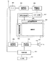
- Publication number
- JP5437626B2 JP5437626B2 JP2008318615A JP2008318615A JP5437626B2 JP 5437626 B2 JP5437626 B2 JP 5437626B2 JP 2008318615 A JP2008318615 A JP 2008318615A JP 2008318615 A JP2008318615 A JP 2008318615A JP 5437626 B2 JP5437626 B2 JP 5437626B2
- Authority
- JP
- Japan
- Prior art keywords
- single crystal
- substrate
- layer
- crystal semiconductor
- semiconductor
- Prior art date
- Legal status (The legal status is an assumption and is not a legal conclusion. Google has not performed a legal analysis and makes no representation as to the accuracy of the status listed.)
- Expired - Fee Related
Links
- 239000004065 semiconductor Substances 0.000 title claims description 683
- 238000004519 manufacturing process Methods 0.000 title claims description 37
- 239000000758 substrate Substances 0.000 claims description 512
- 239000013078 crystal Substances 0.000 claims description 368
- 238000000034 method Methods 0.000 claims description 140
- 229920005989 resin Polymers 0.000 claims description 108
- 239000011347 resin Substances 0.000 claims description 108
- 150000002500 ions Chemical class 0.000 claims description 79
- 238000010438 heat treatment Methods 0.000 claims description 51
- 238000005520 cutting process Methods 0.000 claims description 22
- 239000011521 glass Substances 0.000 claims description 14
- 230000003313 weakening effect Effects 0.000 claims description 8
- 239000010410 layer Substances 0.000 description 522
- 239000010408 film Substances 0.000 description 170
- 239000012535 impurity Substances 0.000 description 57
- 239000007789 gas Substances 0.000 description 51
- VYPSYNLAJGMNEJ-UHFFFAOYSA-N Silicium dioxide Chemical compound O=[Si]=O VYPSYNLAJGMNEJ-UHFFFAOYSA-N 0.000 description 32
- 229910052814 silicon oxide Inorganic materials 0.000 description 31
- 239000011241 protective layer Substances 0.000 description 30
- 239000001257 hydrogen Substances 0.000 description 29
- 229910052739 hydrogen Inorganic materials 0.000 description 29
- 230000008569 process Effects 0.000 description 29
- 239000000463 material Substances 0.000 description 27
- 230000006870 function Effects 0.000 description 26
- 239000004973 liquid crystal related substance Substances 0.000 description 26
- 229910052581 Si3N4 Inorganic materials 0.000 description 25
- HQVNEWCFYHHQES-UHFFFAOYSA-N silicon nitride Chemical compound N12[Si]34N5[Si]62N3[Si]51N64 HQVNEWCFYHHQES-UHFFFAOYSA-N 0.000 description 25
- 238000005530 etching Methods 0.000 description 24
- 229910052710 silicon Inorganic materials 0.000 description 21
- UFHFLCQGNIYNRP-UHFFFAOYSA-N Hydrogen Chemical compound [H][H] UFHFLCQGNIYNRP-UHFFFAOYSA-N 0.000 description 20
- XUIMIQQOPSSXEZ-UHFFFAOYSA-N Silicon Chemical compound [Si] XUIMIQQOPSSXEZ-UHFFFAOYSA-N 0.000 description 20
- 239000010703 silicon Substances 0.000 description 20
- 229910052736 halogen Inorganic materials 0.000 description 19
- 230000007547 defect Effects 0.000 description 18
- -1 silver halide Chemical class 0.000 description 18
- 150000002367 halogens Chemical class 0.000 description 17
- 239000011159 matrix material Substances 0.000 description 17
- 235000012431 wafers Nutrition 0.000 description 16
- 229910052782 aluminium Inorganic materials 0.000 description 15
- 238000005229 chemical vapour deposition Methods 0.000 description 15
- 229910052751 metal Inorganic materials 0.000 description 15
- 239000002184 metal Substances 0.000 description 15
- 239000002245 particle Substances 0.000 description 15
- 238000005498 polishing Methods 0.000 description 15
- 238000012545 processing Methods 0.000 description 15
- 239000000126 substance Substances 0.000 description 15
- 230000002829 reductive effect Effects 0.000 description 14
- XAGFODPZIPBFFR-UHFFFAOYSA-N aluminium Chemical compound [Al] XAGFODPZIPBFFR-UHFFFAOYSA-N 0.000 description 13
- 230000015572 biosynthetic process Effects 0.000 description 13
- 230000000903 blocking effect Effects 0.000 description 13
- XKRFYHLGVUSROY-UHFFFAOYSA-N Argon Chemical compound [Ar] XKRFYHLGVUSROY-UHFFFAOYSA-N 0.000 description 12
- KRHYYFGTRYWZRS-UHFFFAOYSA-N Fluorane Chemical compound F KRHYYFGTRYWZRS-UHFFFAOYSA-N 0.000 description 12
- BLRPTPMANUNPDV-UHFFFAOYSA-N Silane Chemical compound [SiH4] BLRPTPMANUNPDV-UHFFFAOYSA-N 0.000 description 12
- 239000012298 atmosphere Substances 0.000 description 12
- 229910021421 monocrystalline silicon Inorganic materials 0.000 description 12
- 239000001301 oxygen Substances 0.000 description 12
- 229910052760 oxygen Inorganic materials 0.000 description 12
- 239000000460 chlorine Substances 0.000 description 11
- 230000003647 oxidation Effects 0.000 description 11
- 238000007254 oxidation reaction Methods 0.000 description 11
- 238000004544 sputter deposition Methods 0.000 description 11
- IJGRMHOSHXDMSA-UHFFFAOYSA-N Atomic nitrogen Chemical compound N#N IJGRMHOSHXDMSA-UHFFFAOYSA-N 0.000 description 10
- 230000001133 acceleration Effects 0.000 description 10
- 230000001070 adhesive effect Effects 0.000 description 10
- QVGXLLKOCUKJST-UHFFFAOYSA-N atomic oxygen Chemical compound [O] QVGXLLKOCUKJST-UHFFFAOYSA-N 0.000 description 10
- 230000002093 peripheral effect Effects 0.000 description 10
- 229910000077 silane Inorganic materials 0.000 description 10
- 125000004429 atom Chemical group 0.000 description 9
- 238000004140 cleaning Methods 0.000 description 9
- 239000000701 coagulant Substances 0.000 description 9
- 239000011261 inert gas Substances 0.000 description 9
- 238000005468 ion implantation Methods 0.000 description 9
- 229910021420 polycrystalline silicon Inorganic materials 0.000 description 9
- 239000000565 sealant Substances 0.000 description 9
- 239000010409 thin film Substances 0.000 description 9
- GQPLMRYTRLFLPF-UHFFFAOYSA-N Nitrous Oxide Chemical compound [O-][N+]#N GQPLMRYTRLFLPF-UHFFFAOYSA-N 0.000 description 8
- 230000000694 effects Effects 0.000 description 8
- 239000011737 fluorine Substances 0.000 description 8
- 229910052731 fluorine Inorganic materials 0.000 description 8
- 229910052734 helium Inorganic materials 0.000 description 8
- TWNQGVIAIRXVLR-UHFFFAOYSA-N oxo(oxoalumanyloxy)alumane Chemical compound O=[Al]O[Al]=O TWNQGVIAIRXVLR-UHFFFAOYSA-N 0.000 description 8
- 241000894007 species Species 0.000 description 8
- VEXZGXHMUGYJMC-UHFFFAOYSA-N Hydrochloric acid Chemical compound Cl VEXZGXHMUGYJMC-UHFFFAOYSA-N 0.000 description 7
- 229910052786 argon Inorganic materials 0.000 description 7
- 238000003776 cleavage reaction Methods 0.000 description 7
- 239000001307 helium Substances 0.000 description 7
- SWQJXJOGLNCZEY-UHFFFAOYSA-N helium atom Chemical compound [He] SWQJXJOGLNCZEY-UHFFFAOYSA-N 0.000 description 7
- 238000005268 plasma chemical vapour deposition Methods 0.000 description 7
- 229920005591 polysilicon Polymers 0.000 description 7
- 230000007017 scission Effects 0.000 description 7
- ZAMOUSCENKQFHK-UHFFFAOYSA-N Chlorine atom Chemical compound [Cl] ZAMOUSCENKQFHK-UHFFFAOYSA-N 0.000 description 6
- MHAJPDPJQMAIIY-UHFFFAOYSA-N Hydrogen peroxide Chemical compound OO MHAJPDPJQMAIIY-UHFFFAOYSA-N 0.000 description 6
- PXHVJJICTQNCMI-UHFFFAOYSA-N Nickel Chemical compound [Ni] PXHVJJICTQNCMI-UHFFFAOYSA-N 0.000 description 6
- 230000009471 action Effects 0.000 description 6
- 239000000853 adhesive Substances 0.000 description 6
- 239000000956 alloy Substances 0.000 description 6
- 229910052801 chlorine Inorganic materials 0.000 description 6
- 238000000576 coating method Methods 0.000 description 6
- 238000005247 gettering Methods 0.000 description 6
- 239000011777 magnesium Substances 0.000 description 6
- 150000002739 metals Chemical class 0.000 description 6
- 150000001282 organosilanes Chemical class 0.000 description 6
- 239000010936 titanium Substances 0.000 description 6
- 238000007740 vapor deposition Methods 0.000 description 6
- 238000001039 wet etching Methods 0.000 description 6
- OKTJSMMVPCPJKN-UHFFFAOYSA-N Carbon Chemical compound [C] OKTJSMMVPCPJKN-UHFFFAOYSA-N 0.000 description 5
- YCKRFDGAMUMZLT-UHFFFAOYSA-N Fluorine atom Chemical compound [F] YCKRFDGAMUMZLT-UHFFFAOYSA-N 0.000 description 5
- FYYHWMGAXLPEAU-UHFFFAOYSA-N Magnesium Chemical compound [Mg] FYYHWMGAXLPEAU-UHFFFAOYSA-N 0.000 description 5
- 238000005411 Van der Waals force Methods 0.000 description 5
- 229910045601 alloy Inorganic materials 0.000 description 5
- 238000000137 annealing Methods 0.000 description 5
- 239000010949 copper Substances 0.000 description 5
- 238000009792 diffusion process Methods 0.000 description 5
- KPUWHANPEXNPJT-UHFFFAOYSA-N disiloxane Chemical class [SiH3]O[SiH3] KPUWHANPEXNPJT-UHFFFAOYSA-N 0.000 description 5
- 239000010931 gold Substances 0.000 description 5
- 238000000227 grinding Methods 0.000 description 5
- 229910052749 magnesium Inorganic materials 0.000 description 5
- 229910044991 metal oxide Inorganic materials 0.000 description 5
- 150000004706 metal oxides Chemical class 0.000 description 5
- 230000001590 oxidative effect Effects 0.000 description 5
- QGZKDVFQNNGYKY-UHFFFAOYSA-N Ammonia Chemical compound N QGZKDVFQNNGYKY-UHFFFAOYSA-N 0.000 description 4
- KDLHZDBZIXYQEI-UHFFFAOYSA-N Palladium Chemical compound [Pd] KDLHZDBZIXYQEI-UHFFFAOYSA-N 0.000 description 4
- BOTDANWDWHJENH-UHFFFAOYSA-N Tetraethyl orthosilicate Chemical compound CCO[Si](OCC)(OCC)OCC BOTDANWDWHJENH-UHFFFAOYSA-N 0.000 description 4
- GWEVSGVZZGPLCZ-UHFFFAOYSA-N Titan oxide Chemical compound O=[Ti]=O GWEVSGVZZGPLCZ-UHFFFAOYSA-N 0.000 description 4
- 229910021417 amorphous silicon Inorganic materials 0.000 description 4
- 229910052799 carbon Inorganic materials 0.000 description 4
- 239000000919 ceramic Substances 0.000 description 4
- 230000008859 change Effects 0.000 description 4
- 238000006243 chemical reaction Methods 0.000 description 4
- 239000004020 conductor Substances 0.000 description 4
- 238000002425 crystallisation Methods 0.000 description 4
- 238000000151 deposition Methods 0.000 description 4
- 230000005669 field effect Effects 0.000 description 4
- 229910052737 gold Inorganic materials 0.000 description 4
- 229910000041 hydrogen chloride Inorganic materials 0.000 description 4
- IXCSERBJSXMMFS-UHFFFAOYSA-N hydrogen chloride Substances Cl.Cl IXCSERBJSXMMFS-UHFFFAOYSA-N 0.000 description 4
- 230000006386 memory function Effects 0.000 description 4
- 229910052757 nitrogen Inorganic materials 0.000 description 4
- 239000001272 nitrous oxide Substances 0.000 description 4
- 238000009832 plasma treatment Methods 0.000 description 4
- BASFCYQUMIYNBI-UHFFFAOYSA-N platinum Chemical compound [Pt] BASFCYQUMIYNBI-UHFFFAOYSA-N 0.000 description 4
- 238000007517 polishing process Methods 0.000 description 4
- 230000001681 protective effect Effects 0.000 description 4
- 239000002994 raw material Substances 0.000 description 4
- 230000002441 reversible effect Effects 0.000 description 4
- 238000000926 separation method Methods 0.000 description 4
- 230000005236 sound signal Effects 0.000 description 4
- 229910052712 strontium Inorganic materials 0.000 description 4
- CIOAGBVUUVVLOB-UHFFFAOYSA-N strontium atom Chemical compound [Sr] CIOAGBVUUVVLOB-UHFFFAOYSA-N 0.000 description 4
- IATRAKWUXMZMIY-UHFFFAOYSA-N strontium oxide Chemical compound [O-2].[Sr+2] IATRAKWUXMZMIY-UHFFFAOYSA-N 0.000 description 4
- WGTYBPLFGIVFAS-UHFFFAOYSA-M tetramethylammonium hydroxide Chemical compound [OH-].C[N+](C)(C)C WGTYBPLFGIVFAS-UHFFFAOYSA-M 0.000 description 4
- 229920001187 thermosetting polymer Polymers 0.000 description 4
- JBRZTFJDHDCESZ-UHFFFAOYSA-N AsGa Chemical compound [As]#[Ga] JBRZTFJDHDCESZ-UHFFFAOYSA-N 0.000 description 3
- 229910001218 Gallium arsenide Inorganic materials 0.000 description 3
- OAICVXFJPJFONN-UHFFFAOYSA-N Phosphorus Chemical compound [P] OAICVXFJPJFONN-UHFFFAOYSA-N 0.000 description 3
- 239000004642 Polyimide Substances 0.000 description 3
- 229910003902 SiCl 4 Inorganic materials 0.000 description 3
- NIXOWILDQLNWCW-UHFFFAOYSA-N acrylic acid group Chemical group C(C=C)(=O)O NIXOWILDQLNWCW-UHFFFAOYSA-N 0.000 description 3
- 150000001805 chlorine compounds Chemical class 0.000 description 3
- 150000001875 compounds Chemical class 0.000 description 3
- 229910052802 copper Inorganic materials 0.000 description 3
- 230000008025 crystallization Effects 0.000 description 3
- 238000001723 curing Methods 0.000 description 3
- 230000008021 deposition Effects 0.000 description 3
- 238000001312 dry etching Methods 0.000 description 3
- 230000009977 dual effect Effects 0.000 description 3
- 239000000428 dust Substances 0.000 description 3
- 238000005401 electroluminescence Methods 0.000 description 3
- 239000003822 epoxy resin Substances 0.000 description 3
- 230000006355 external stress Effects 0.000 description 3
- 229910052732 germanium Inorganic materials 0.000 description 3
- PCHJSUWPFVWCPO-UHFFFAOYSA-N gold Chemical compound [Au] PCHJSUWPFVWCPO-UHFFFAOYSA-N 0.000 description 3
- AMGQUBHHOARCQH-UHFFFAOYSA-N indium;oxotin Chemical compound [In].[Sn]=O AMGQUBHHOARCQH-UHFFFAOYSA-N 0.000 description 3
- 238000010884 ion-beam technique Methods 0.000 description 3
- 230000001678 irradiating effect Effects 0.000 description 3
- 229910052743 krypton Inorganic materials 0.000 description 3
- 230000007246 mechanism Effects 0.000 description 3
- 229910052754 neon Inorganic materials 0.000 description 3
- 229910052759 nickel Inorganic materials 0.000 description 3
- 239000012299 nitrogen atmosphere Substances 0.000 description 3
- 230000003287 optical effect Effects 0.000 description 3
- 150000002894 organic compounds Chemical class 0.000 description 3
- 239000012071 phase Substances 0.000 description 3
- 229910052698 phosphorus Inorganic materials 0.000 description 3
- 239000011574 phosphorus Substances 0.000 description 3
- 238000000016 photochemical curing Methods 0.000 description 3
- 229920003023 plastic Polymers 0.000 description 3
- 239000004033 plastic Substances 0.000 description 3
- 229920000647 polyepoxide Polymers 0.000 description 3
- 229920006267 polyester film Polymers 0.000 description 3
- 229920001721 polyimide Polymers 0.000 description 3
- 229920002620 polyvinyl fluoride Polymers 0.000 description 3
- 238000007639 printing Methods 0.000 description 3
- 230000003252 repetitive effect Effects 0.000 description 3
- 229910052709 silver Inorganic materials 0.000 description 3
- 229910000679 solder Inorganic materials 0.000 description 3
- 230000035882 stress Effects 0.000 description 3
- 229910052715 tantalum Inorganic materials 0.000 description 3
- 229910052719 titanium Inorganic materials 0.000 description 3
- XLYOFNOQVPJJNP-UHFFFAOYSA-N water Substances O XLYOFNOQVPJJNP-UHFFFAOYSA-N 0.000 description 3
- 229910052724 xenon Inorganic materials 0.000 description 3
- WZJUBBHODHNQPW-UHFFFAOYSA-N 2,4,6,8-tetramethyl-1,3,5,7,2$l^{3},4$l^{3},6$l^{3},8$l^{3}-tetraoxatetrasilocane Chemical compound C[Si]1O[Si](C)O[Si](C)O[Si](C)O1 WZJUBBHODHNQPW-UHFFFAOYSA-N 0.000 description 2
- DDFHBQSCUXNBSA-UHFFFAOYSA-N 5-(5-carboxythiophen-2-yl)thiophene-2-carboxylic acid Chemical compound S1C(C(=O)O)=CC=C1C1=CC=C(C(O)=O)S1 DDFHBQSCUXNBSA-UHFFFAOYSA-N 0.000 description 2
- 239000004925 Acrylic resin Substances 0.000 description 2
- 229920000178 Acrylic resin Polymers 0.000 description 2
- ZOXJGFHDIHLPTG-UHFFFAOYSA-N Boron Chemical compound [B] ZOXJGFHDIHLPTG-UHFFFAOYSA-N 0.000 description 2
- RYGMFSIKBFXOCR-UHFFFAOYSA-N Copper Chemical compound [Cu] RYGMFSIKBFXOCR-UHFFFAOYSA-N 0.000 description 2
- GPXJNWSHGFTCBW-UHFFFAOYSA-N Indium phosphide Chemical compound [In]#P GPXJNWSHGFTCBW-UHFFFAOYSA-N 0.000 description 2
- ZOKXTWBITQBERF-UHFFFAOYSA-N Molybdenum Chemical compound [Mo] ZOKXTWBITQBERF-UHFFFAOYSA-N 0.000 description 2
- 238000001237 Raman spectrum Methods 0.000 description 2
- 229910002808 Si–O–Si Inorganic materials 0.000 description 2
- QAOWNCQODCNURD-UHFFFAOYSA-N Sulfuric acid Chemical compound OS(O)(=O)=O QAOWNCQODCNURD-UHFFFAOYSA-N 0.000 description 2
- RTAQQCXQSZGOHL-UHFFFAOYSA-N Titanium Chemical compound [Ti] RTAQQCXQSZGOHL-UHFFFAOYSA-N 0.000 description 2
- 229910021529 ammonia Inorganic materials 0.000 description 2
- 229910052788 barium Inorganic materials 0.000 description 2
- 239000011230 binding agent Substances 0.000 description 2
- 229910052796 boron Inorganic materials 0.000 description 2
- DQXBYHZEEUGOBF-UHFFFAOYSA-N but-3-enoic acid;ethene Chemical compound C=C.OC(=O)CC=C DQXBYHZEEUGOBF-UHFFFAOYSA-N 0.000 description 2
- 239000003990 capacitor Substances 0.000 description 2
- 150000001768 cations Chemical class 0.000 description 2
- 239000011651 chromium Substances 0.000 description 2
- 239000011248 coating agent Substances 0.000 description 2
- 238000004891 communication Methods 0.000 description 2
- 230000000295 complement effect Effects 0.000 description 2
- 238000011109 contamination Methods 0.000 description 2
- 238000010586 diagram Methods 0.000 description 2
- 238000007598 dipping method Methods 0.000 description 2
- 230000005684 electric field Effects 0.000 description 2
- 238000010894 electron beam technology Methods 0.000 description 2
- 229920006332 epoxy adhesive Polymers 0.000 description 2
- 239000005038 ethylene vinyl acetate Substances 0.000 description 2
- 230000005281 excited state Effects 0.000 description 2
- 239000011152 fibreglass Substances 0.000 description 2
- 239000000945 filler Substances 0.000 description 2
- 239000010419 fine particle Substances 0.000 description 2
- 125000001153 fluoro group Chemical group F* 0.000 description 2
- GNPVGFCGXDBREM-UHFFFAOYSA-N germanium atom Chemical compound [Ge] GNPVGFCGXDBREM-UHFFFAOYSA-N 0.000 description 2
- 150000002431 hydrogen Chemical class 0.000 description 2
- 238000005984 hydrogenation reaction Methods 0.000 description 2
- 229910003437 indium oxide Inorganic materials 0.000 description 2
- PJXISJQVUVHSOJ-UHFFFAOYSA-N indium(iii) oxide Chemical compound [O-2].[O-2].[O-2].[In+3].[In+3] PJXISJQVUVHSOJ-UHFFFAOYSA-N 0.000 description 2
- 238000002347 injection Methods 0.000 description 2
- 239000007924 injection Substances 0.000 description 2
- 239000011810 insulating material Substances 0.000 description 2
- 239000011229 interlayer Substances 0.000 description 2
- DNNSSWSSYDEUBZ-UHFFFAOYSA-N krypton atom Chemical compound [Kr] DNNSSWSSYDEUBZ-UHFFFAOYSA-N 0.000 description 2
- 239000002346 layers by function Substances 0.000 description 2
- 239000007788 liquid Substances 0.000 description 2
- 239000000395 magnesium oxide Substances 0.000 description 2
- CPLXHLVBOLITMK-UHFFFAOYSA-N magnesium oxide Inorganic materials [Mg]=O CPLXHLVBOLITMK-UHFFFAOYSA-N 0.000 description 2
- AXZKOIWUVFPNLO-UHFFFAOYSA-N magnesium;oxygen(2-) Chemical compound [O-2].[Mg+2] AXZKOIWUVFPNLO-UHFFFAOYSA-N 0.000 description 2
- 239000003550 marker Substances 0.000 description 2
- 239000002923 metal particle Substances 0.000 description 2
- 229910021424 microcrystalline silicon Inorganic materials 0.000 description 2
- 239000011259 mixed solution Substances 0.000 description 2
- 229910052750 molybdenum Inorganic materials 0.000 description 2
- 239000011733 molybdenum Substances 0.000 description 2
- GKAOGPIIYCISHV-UHFFFAOYSA-N neon atom Chemical compound [Ne] GKAOGPIIYCISHV-UHFFFAOYSA-N 0.000 description 2
- QGLKJKCYBOYXKC-UHFFFAOYSA-N nonaoxidotritungsten Chemical compound O=[W]1(=O)O[W](=O)(=O)O[W](=O)(=O)O1 QGLKJKCYBOYXKC-UHFFFAOYSA-N 0.000 description 2
- HMMGMWAXVFQUOA-UHFFFAOYSA-N octamethylcyclotetrasiloxane Chemical compound C[Si]1(C)O[Si](C)(C)O[Si](C)(C)O[Si](C)(C)O1 HMMGMWAXVFQUOA-UHFFFAOYSA-N 0.000 description 2
- 125000000962 organic group Chemical group 0.000 description 2
- 229910052763 palladium Inorganic materials 0.000 description 2
- 238000001020 plasma etching Methods 0.000 description 2
- 229910052697 platinum Inorganic materials 0.000 description 2
- 229920001200 poly(ethylene-vinyl acetate) Polymers 0.000 description 2
- 229920002037 poly(vinyl butyral) polymer Polymers 0.000 description 2
- 229920000915 polyvinyl chloride Polymers 0.000 description 2
- 239000004800 polyvinyl chloride Substances 0.000 description 2
- 229910021426 porous silicon Inorganic materials 0.000 description 2
- 150000003254 radicals Chemical class 0.000 description 2
- 238000004151 rapid thermal annealing Methods 0.000 description 2
- 230000009467 reduction Effects 0.000 description 2
- 238000007650 screen-printing Methods 0.000 description 2
- 239000011359 shock absorbing material Substances 0.000 description 2
- 229910021332 silicide Inorganic materials 0.000 description 2
- FVBUAEGBCNSCDD-UHFFFAOYSA-N silicide(4-) Chemical compound [Si-4] FVBUAEGBCNSCDD-UHFFFAOYSA-N 0.000 description 2
- 239000013464 silicone adhesive Substances 0.000 description 2
- 239000004332 silver Substances 0.000 description 2
- 239000002356 single layer Substances 0.000 description 2
- 239000007790 solid phase Substances 0.000 description 2
- 125000006850 spacer group Chemical group 0.000 description 2
- 238000005507 spraying Methods 0.000 description 2
- 238000004381 surface treatment Methods 0.000 description 2
- GUVRBAGPIYLISA-UHFFFAOYSA-N tantalum atom Chemical compound [Ta] GUVRBAGPIYLISA-UHFFFAOYSA-N 0.000 description 2
- CZDYPVPMEAXLPK-UHFFFAOYSA-N tetramethylsilane Chemical compound C[Si](C)(C)C CZDYPVPMEAXLPK-UHFFFAOYSA-N 0.000 description 2
- 238000002230 thermal chemical vapour deposition Methods 0.000 description 2
- OGIDPMRJRNCKJF-UHFFFAOYSA-N titanium oxide Inorganic materials [Ti]=O OGIDPMRJRNCKJF-UHFFFAOYSA-N 0.000 description 2
- 238000012546 transfer Methods 0.000 description 2
- 229910052721 tungsten Inorganic materials 0.000 description 2
- 229910001930 tungsten oxide Inorganic materials 0.000 description 2
- 238000004506 ultrasonic cleaning Methods 0.000 description 2
- FHNFHKCVQCLJFQ-UHFFFAOYSA-N xenon atom Chemical compound [Xe] FHNFHKCVQCLJFQ-UHFFFAOYSA-N 0.000 description 2
- YVTHLONGBIQYBO-UHFFFAOYSA-N zinc indium(3+) oxygen(2-) Chemical compound [O--].[Zn++].[In+3] YVTHLONGBIQYBO-UHFFFAOYSA-N 0.000 description 2
- MGWGWNFMUOTEHG-UHFFFAOYSA-N 4-(3,5-dimethylphenyl)-1,3-thiazol-2-amine Chemical compound CC1=CC(C)=CC(C=2N=C(N)SC=2)=C1 MGWGWNFMUOTEHG-UHFFFAOYSA-N 0.000 description 1
- 229910017073 AlLi Inorganic materials 0.000 description 1
- PIGFYZPCRLYGLF-UHFFFAOYSA-N Aluminum nitride Chemical compound [Al]#N PIGFYZPCRLYGLF-UHFFFAOYSA-N 0.000 description 1
- VYZAMTAEIAYCRO-UHFFFAOYSA-N Chromium Chemical compound [Cr] VYZAMTAEIAYCRO-UHFFFAOYSA-N 0.000 description 1
- GYHNNYVSQQEPJS-UHFFFAOYSA-N Gallium Chemical compound [Ga] GYHNNYVSQQEPJS-UHFFFAOYSA-N 0.000 description 1
- 206010052128 Glare Diseases 0.000 description 1
- DGAQECJNVWCQMB-PUAWFVPOSA-M Ilexoside XXIX Chemical compound C[C@@H]1CC[C@@]2(CC[C@@]3(C(=CC[C@H]4[C@]3(CC[C@@H]5[C@@]4(CC[C@@H](C5(C)C)OS(=O)(=O)[O-])C)C)[C@@H]2[C@]1(C)O)C)C(=O)O[C@H]6[C@@H]([C@H]([C@@H]([C@H](O6)CO)O)O)O.[Na+] DGAQECJNVWCQMB-PUAWFVPOSA-M 0.000 description 1
- 239000004640 Melamine resin Substances 0.000 description 1
- 229920000877 Melamine resin Polymers 0.000 description 1
- 229910052779 Neodymium Inorganic materials 0.000 description 1
- CBENFWSGALASAD-UHFFFAOYSA-N Ozone Chemical compound [O-][O+]=O CBENFWSGALASAD-UHFFFAOYSA-N 0.000 description 1
- XYFCBTPGUUZFHI-UHFFFAOYSA-N Phosphine Chemical compound P XYFCBTPGUUZFHI-UHFFFAOYSA-N 0.000 description 1
- 239000004952 Polyamide Substances 0.000 description 1
- BQCADISMDOOEFD-UHFFFAOYSA-N Silver Chemical compound [Ag] BQCADISMDOOEFD-UHFFFAOYSA-N 0.000 description 1
- 241000862969 Stella Species 0.000 description 1
- MCMNRKCIXSYSNV-UHFFFAOYSA-N ZrO2 Inorganic materials O=[Zr]=O MCMNRKCIXSYSNV-UHFFFAOYSA-N 0.000 description 1
- LEVVHYCKPQWKOP-UHFFFAOYSA-N [Si].[Ge] Chemical compound [Si].[Ge] LEVVHYCKPQWKOP-UHFFFAOYSA-N 0.000 description 1
- 230000004913 activation Effects 0.000 description 1
- 239000012790 adhesive layer Substances 0.000 description 1
- 230000002411 adverse Effects 0.000 description 1
- 125000000217 alkyl group Chemical group 0.000 description 1
- 239000005407 aluminoborosilicate glass Substances 0.000 description 1
- 239000005354 aluminosilicate glass Substances 0.000 description 1
- 150000001408 amides Chemical class 0.000 description 1
- 230000003321 amplification Effects 0.000 description 1
- 239000007864 aqueous solution Substances 0.000 description 1
- 229910052785 arsenic Inorganic materials 0.000 description 1
- RQNWIZPPADIBDY-UHFFFAOYSA-N arsenic atom Chemical compound [As] RQNWIZPPADIBDY-UHFFFAOYSA-N 0.000 description 1
- 125000003118 aryl group Chemical group 0.000 description 1
- 238000001505 atmospheric-pressure chemical vapour deposition Methods 0.000 description 1
- LDDQLRUQCUTJBB-UHFFFAOYSA-O azanium;hydrofluoride Chemical compound [NH4+].F LDDQLRUQCUTJBB-UHFFFAOYSA-O 0.000 description 1
- DSAJWYNOEDNPEQ-UHFFFAOYSA-N barium atom Chemical compound [Ba] DSAJWYNOEDNPEQ-UHFFFAOYSA-N 0.000 description 1
- 230000004888 barrier function Effects 0.000 description 1
- UMIVXZPTRXBADB-UHFFFAOYSA-N benzocyclobutene Chemical compound C1=CC=C2CCC2=C1 UMIVXZPTRXBADB-UHFFFAOYSA-N 0.000 description 1
- 239000005388 borosilicate glass Substances 0.000 description 1
- 229910052791 calcium Inorganic materials 0.000 description 1
- 239000002041 carbon nanotube Substances 0.000 description 1
- 229910021393 carbon nanotube Inorganic materials 0.000 description 1
- 239000000969 carrier Substances 0.000 description 1
- 230000001413 cellular effect Effects 0.000 description 1
- 239000003795 chemical substances by application Substances 0.000 description 1
- SLLGVCUQYRMELA-UHFFFAOYSA-N chlorosilicon Chemical compound Cl[Si] SLLGVCUQYRMELA-UHFFFAOYSA-N 0.000 description 1
- 229910052804 chromium Inorganic materials 0.000 description 1
- 239000003086 colorant Substances 0.000 description 1
- 239000000356 contaminant Substances 0.000 description 1
- PMHQVHHXPFUNSP-UHFFFAOYSA-M copper(1+);methylsulfanylmethane;bromide Chemical compound Br[Cu].CSC PMHQVHHXPFUNSP-UHFFFAOYSA-M 0.000 description 1
- 238000007872 degassing Methods 0.000 description 1
- 238000013461 design Methods 0.000 description 1
- 239000010432 diamond Substances 0.000 description 1
- 229910003460 diamond Inorganic materials 0.000 description 1
- ZOCHARZZJNPSEU-UHFFFAOYSA-N diboron Chemical compound B#B ZOCHARZZJNPSEU-UHFFFAOYSA-N 0.000 description 1
- 238000007865 diluting Methods 0.000 description 1
- 229910001873 dinitrogen Inorganic materials 0.000 description 1
- PZPGRFITIJYNEJ-UHFFFAOYSA-N disilane Chemical compound [SiH3][SiH3] PZPGRFITIJYNEJ-UHFFFAOYSA-N 0.000 description 1
- 239000002270 dispersing agent Substances 0.000 description 1
- 238000006073 displacement reaction Methods 0.000 description 1
- 238000009429 electrical wiring Methods 0.000 description 1
- 238000009713 electroplating Methods 0.000 description 1
- 239000012530 fluid Substances 0.000 description 1
- 239000011888 foil Substances 0.000 description 1
- 230000008014 freezing Effects 0.000 description 1
- 238000007710 freezing Methods 0.000 description 1
- 229910052733 gallium Inorganic materials 0.000 description 1
- 229910000078 germane Inorganic materials 0.000 description 1
- 230000005283 ground state Effects 0.000 description 1
- 229910021480 group 4 element Inorganic materials 0.000 description 1
- 229910000449 hafnium oxide Inorganic materials 0.000 description 1
- WIHZLLGSGQNAGK-UHFFFAOYSA-N hafnium(4+);oxygen(2-) Chemical compound [O-2].[O-2].[Hf+4] WIHZLLGSGQNAGK-UHFFFAOYSA-N 0.000 description 1
- FFUAGWLWBBFQJT-UHFFFAOYSA-N hexamethyldisilazane Chemical compound C[Si](C)(C)N[Si](C)(C)C FFUAGWLWBBFQJT-UHFFFAOYSA-N 0.000 description 1
- 230000005525 hole transport Effects 0.000 description 1
- GPRLSGONYQIRFK-UHFFFAOYSA-N hydron Chemical compound [H+] GPRLSGONYQIRFK-UHFFFAOYSA-N 0.000 description 1
- 230000005660 hydrophilic surface Effects 0.000 description 1
- 230000001771 impaired effect Effects 0.000 description 1
- 150000002484 inorganic compounds Chemical class 0.000 description 1
- 229910010272 inorganic material Inorganic materials 0.000 description 1
- 238000009434 installation Methods 0.000 description 1
- 229910052741 iridium Inorganic materials 0.000 description 1
- 229910052742 iron Inorganic materials 0.000 description 1
- XEEYBQQBJWHFJM-UHFFFAOYSA-N iron Substances [Fe] XEEYBQQBJWHFJM-UHFFFAOYSA-N 0.000 description 1
- 238000005499 laser crystallization Methods 0.000 description 1
- 238000003698 laser cutting Methods 0.000 description 1
- 238000004518 low pressure chemical vapour deposition Methods 0.000 description 1
- 238000005259 measurement Methods 0.000 description 1
- 238000002844 melting Methods 0.000 description 1
- 230000008018 melting Effects 0.000 description 1
- QSHDDOUJBYECFT-UHFFFAOYSA-N mercury Chemical compound [Hg] QSHDDOUJBYECFT-UHFFFAOYSA-N 0.000 description 1
- 229910052753 mercury Inorganic materials 0.000 description 1
- 229910001507 metal halide Inorganic materials 0.000 description 1
- 150000005309 metal halides Chemical class 0.000 description 1
- 229910021645 metal ion Inorganic materials 0.000 description 1
- 239000000203 mixture Substances 0.000 description 1
- QEFYFXOXNSNQGX-UHFFFAOYSA-N neodymium atom Chemical compound [Nd] QEFYFXOXNSNQGX-UHFFFAOYSA-N 0.000 description 1
- 230000007935 neutral effect Effects 0.000 description 1
- 150000004767 nitrides Chemical class 0.000 description 1
- 238000005121 nitriding Methods 0.000 description 1
- JCXJVPUVTGWSNB-UHFFFAOYSA-N nitrogen dioxide Inorganic materials O=[N]=O JCXJVPUVTGWSNB-UHFFFAOYSA-N 0.000 description 1
- 150000002831 nitrogen free-radicals Chemical class 0.000 description 1
- QJGQUHMNIGDVPM-UHFFFAOYSA-N nitrogen group Chemical group [N] QJGQUHMNIGDVPM-UHFFFAOYSA-N 0.000 description 1
- 229920003986 novolac Polymers 0.000 description 1
- 238000003199 nucleic acid amplification method Methods 0.000 description 1
- 238000007645 offset printing Methods 0.000 description 1
- 239000012788 optical film Substances 0.000 description 1
- 239000011368 organic material Substances 0.000 description 1
- AHLBNYSZXLDEJQ-FWEHEUNISA-N orlistat Chemical compound CCCCCCCCCCC[C@H](OC(=O)[C@H](CC(C)C)NC=O)C[C@@H]1OC(=O)[C@H]1CCCCCC AHLBNYSZXLDEJQ-FWEHEUNISA-N 0.000 description 1
- 230000010355 oscillation Effects 0.000 description 1
- BPUBBGLMJRNUCC-UHFFFAOYSA-N oxygen(2-);tantalum(5+) Chemical compound [O-2].[O-2].[O-2].[O-2].[O-2].[Ta+5].[Ta+5] BPUBBGLMJRNUCC-UHFFFAOYSA-N 0.000 description 1
- RVTZCBVAJQQJTK-UHFFFAOYSA-N oxygen(2-);zirconium(4+) Chemical compound [O-2].[O-2].[Zr+4] RVTZCBVAJQQJTK-UHFFFAOYSA-N 0.000 description 1
- 230000036961 partial effect Effects 0.000 description 1
- SLIUAWYAILUBJU-UHFFFAOYSA-N pentacene Chemical compound C1=CC=CC2=CC3=CC4=CC5=CC=CC=C5C=C4C=C3C=C21 SLIUAWYAILUBJU-UHFFFAOYSA-N 0.000 description 1
- 239000005011 phenolic resin Substances 0.000 description 1
- 229920002120 photoresistant polymer Polymers 0.000 description 1
- 238000005240 physical vapour deposition Methods 0.000 description 1
- 229920002647 polyamide Polymers 0.000 description 1
- 229920001709 polysilazane Polymers 0.000 description 1
- 238000003825 pressing Methods 0.000 description 1
- 230000003405 preventing effect Effects 0.000 description 1
- 239000010453 quartz Substances 0.000 description 1
- 238000001552 radio frequency sputter deposition Methods 0.000 description 1
- 238000005546 reactive sputtering Methods 0.000 description 1
- 230000006798 recombination Effects 0.000 description 1
- 238000005215 recombination Methods 0.000 description 1
- 238000004064 recycling Methods 0.000 description 1
- 230000001172 regenerating effect Effects 0.000 description 1
- 230000008929 regeneration Effects 0.000 description 1
- 238000011069 regeneration method Methods 0.000 description 1
- 229910052703 rhodium Inorganic materials 0.000 description 1
- 239000003566 sealing material Substances 0.000 description 1
- 229910052990 silicon hydride Inorganic materials 0.000 description 1
- 239000002210 silicon-based material Substances 0.000 description 1
- 239000010944 silver (metal) Substances 0.000 description 1
- 239000011734 sodium Substances 0.000 description 1
- 229910052708 sodium Inorganic materials 0.000 description 1
- 229910001415 sodium ion Inorganic materials 0.000 description 1
- 238000003746 solid phase reaction Methods 0.000 description 1
- 239000000243 solution Substances 0.000 description 1
- 239000002904 solvent Substances 0.000 description 1
- 238000004528 spin coating Methods 0.000 description 1
- 239000007921 spray Substances 0.000 description 1
- 238000000992 sputter etching Methods 0.000 description 1
- 239000010935 stainless steel Substances 0.000 description 1
- 229910001220 stainless steel Inorganic materials 0.000 description 1
- 125000001424 substituent group Chemical group 0.000 description 1
- 239000004094 surface-active agent Substances 0.000 description 1
- PBCFLUZVCVVTBY-UHFFFAOYSA-N tantalum pentoxide Inorganic materials O=[Ta](=O)O[Ta](=O)=O PBCFLUZVCVVTBY-UHFFFAOYSA-N 0.000 description 1
- 239000013077 target material Substances 0.000 description 1
- 229920002803 thermoplastic polyurethane Polymers 0.000 description 1
- 239000004408 titanium dioxide Substances 0.000 description 1
- 230000007704 transition Effects 0.000 description 1
- QQQSFSZALRVCSZ-UHFFFAOYSA-N triethoxysilane Chemical compound CCO[SiH](OCC)OCC QQQSFSZALRVCSZ-UHFFFAOYSA-N 0.000 description 1
- PQDJYEQOELDLCP-UHFFFAOYSA-N trimethylsilane Chemical compound C[SiH](C)C PQDJYEQOELDLCP-UHFFFAOYSA-N 0.000 description 1
- VEDJZFSRVVQBIL-UHFFFAOYSA-N trisilane Chemical compound [SiH3][SiH2][SiH3] VEDJZFSRVVQBIL-UHFFFAOYSA-N 0.000 description 1
- WFKWXMTUELFFGS-UHFFFAOYSA-N tungsten Chemical compound [W] WFKWXMTUELFFGS-UHFFFAOYSA-N 0.000 description 1
- 239000010937 tungsten Substances 0.000 description 1
- 238000001947 vapour-phase growth Methods 0.000 description 1
- 125000000391 vinyl group Chemical group [H]C([*])=C([H])[H] 0.000 description 1
- 229920002554 vinyl polymer Polymers 0.000 description 1
- 229910052725 zinc Inorganic materials 0.000 description 1
- 239000011701 zinc Substances 0.000 description 1
- 229910052726 zirconium Inorganic materials 0.000 description 1
Images


Classifications
-
- H—ELECTRICITY
- H01—ELECTRIC ELEMENTS
- H01L—SEMICONDUCTOR DEVICES NOT COVERED BY CLASS H10
- H01L27/00—Devices consisting of a plurality of semiconductor or other solid-state components formed in or on a common substrate
- H01L27/02—Devices consisting of a plurality of semiconductor or other solid-state components formed in or on a common substrate including semiconductor components specially adapted for rectifying, oscillating, amplifying or switching and having at least one potential-jump barrier or surface barrier; including integrated passive circuit elements with at least one potential-jump barrier or surface barrier
- H01L27/12—Devices consisting of a plurality of semiconductor or other solid-state components formed in or on a common substrate including semiconductor components specially adapted for rectifying, oscillating, amplifying or switching and having at least one potential-jump barrier or surface barrier; including integrated passive circuit elements with at least one potential-jump barrier or surface barrier the substrate being other than a semiconductor body, e.g. an insulating body
- H01L27/1214—Devices consisting of a plurality of semiconductor or other solid-state components formed in or on a common substrate including semiconductor components specially adapted for rectifying, oscillating, amplifying or switching and having at least one potential-jump barrier or surface barrier; including integrated passive circuit elements with at least one potential-jump barrier or surface barrier the substrate being other than a semiconductor body, e.g. an insulating body comprising a plurality of TFTs formed on a non-semiconducting substrate, e.g. driving circuits for AMLCDs
- H01L27/1259—Multistep manufacturing methods
- H01L27/1262—Multistep manufacturing methods with a particular formation, treatment or coating of the substrate
- H01L27/1266—Multistep manufacturing methods with a particular formation, treatment or coating of the substrate the substrate on which the devices are formed not being the final device substrate, e.g. using a temporary substrate
-
- H—ELECTRICITY
- H01—ELECTRIC ELEMENTS
- H01L—SEMICONDUCTOR DEVICES NOT COVERED BY CLASS H10
- H01L21/00—Processes or apparatus adapted for the manufacture or treatment of semiconductor or solid state devices or of parts thereof
- H01L21/70—Manufacture or treatment of devices consisting of a plurality of solid state components formed in or on a common substrate or of parts thereof; Manufacture of integrated circuit devices or of parts thereof
- H01L21/71—Manufacture of specific parts of devices defined in group H01L21/70
- H01L21/76—Making of isolation regions between components
- H01L21/762—Dielectric regions, e.g. EPIC dielectric isolation, LOCOS; Trench refilling techniques, SOI technology, use of channel stoppers
- H01L21/7624—Dielectric regions, e.g. EPIC dielectric isolation, LOCOS; Trench refilling techniques, SOI technology, use of channel stoppers using semiconductor on insulator [SOI] technology
- H01L21/76251—Dielectric regions, e.g. EPIC dielectric isolation, LOCOS; Trench refilling techniques, SOI technology, use of channel stoppers using semiconductor on insulator [SOI] technology using bonding techniques
- H01L21/76254—Dielectric regions, e.g. EPIC dielectric isolation, LOCOS; Trench refilling techniques, SOI technology, use of channel stoppers using semiconductor on insulator [SOI] technology using bonding techniques with separation/delamination along an ion implanted layer, e.g. Smart-cut, Unibond
-
- H—ELECTRICITY
- H01—ELECTRIC ELEMENTS
- H01L—SEMICONDUCTOR DEVICES NOT COVERED BY CLASS H10
- H01L27/00—Devices consisting of a plurality of semiconductor or other solid-state components formed in or on a common substrate
- H01L27/02—Devices consisting of a plurality of semiconductor or other solid-state components formed in or on a common substrate including semiconductor components specially adapted for rectifying, oscillating, amplifying or switching and having at least one potential-jump barrier or surface barrier; including integrated passive circuit elements with at least one potential-jump barrier or surface barrier
- H01L27/12—Devices consisting of a plurality of semiconductor or other solid-state components formed in or on a common substrate including semiconductor components specially adapted for rectifying, oscillating, amplifying or switching and having at least one potential-jump barrier or surface barrier; including integrated passive circuit elements with at least one potential-jump barrier or surface barrier the substrate being other than a semiconductor body, e.g. an insulating body
- H01L27/1214—Devices consisting of a plurality of semiconductor or other solid-state components formed in or on a common substrate including semiconductor components specially adapted for rectifying, oscillating, amplifying or switching and having at least one potential-jump barrier or surface barrier; including integrated passive circuit elements with at least one potential-jump barrier or surface barrier the substrate being other than a semiconductor body, e.g. an insulating body comprising a plurality of TFTs formed on a non-semiconducting substrate, e.g. driving circuits for AMLCDs
-
- H—ELECTRICITY
- H01—ELECTRIC ELEMENTS
- H01L—SEMICONDUCTOR DEVICES NOT COVERED BY CLASS H10
- H01L2224/00—Indexing scheme for arrangements for connecting or disconnecting semiconductor or solid-state bodies and methods related thereto as covered by H01L24/00
- H01L2224/01—Means for bonding being attached to, or being formed on, the surface to be connected, e.g. chip-to-package, die-attach, "first-level" interconnects; Manufacturing methods related thereto
- H01L2224/42—Wire connectors; Manufacturing methods related thereto
- H01L2224/47—Structure, shape, material or disposition of the wire connectors after the connecting process
- H01L2224/48—Structure, shape, material or disposition of the wire connectors after the connecting process of an individual wire connector
- H01L2224/4805—Shape
- H01L2224/4809—Loop shape
- H01L2224/48091—Arched
-
- H—ELECTRICITY
- H01—ELECTRIC ELEMENTS
- H01L—SEMICONDUCTOR DEVICES NOT COVERED BY CLASS H10
- H01L2224/00—Indexing scheme for arrangements for connecting or disconnecting semiconductor or solid-state bodies and methods related thereto as covered by H01L24/00
- H01L2224/01—Means for bonding being attached to, or being formed on, the surface to be connected, e.g. chip-to-package, die-attach, "first-level" interconnects; Manufacturing methods related thereto
- H01L2224/42—Wire connectors; Manufacturing methods related thereto
- H01L2224/47—Structure, shape, material or disposition of the wire connectors after the connecting process
- H01L2224/48—Structure, shape, material or disposition of the wire connectors after the connecting process of an individual wire connector
- H01L2224/484—Connecting portions
- H01L2224/48463—Connecting portions the connecting portion on the bonding area of the semiconductor or solid-state body being a ball bond
- H01L2224/48464—Connecting portions the connecting portion on the bonding area of the semiconductor or solid-state body being a ball bond the other connecting portion not on the bonding area also being a ball bond, i.e. ball-to-ball
-
- H—ELECTRICITY
- H01—ELECTRIC ELEMENTS
- H01L—SEMICONDUCTOR DEVICES NOT COVERED BY CLASS H10
- H01L2224/00—Indexing scheme for arrangements for connecting or disconnecting semiconductor or solid-state bodies and methods related thereto as covered by H01L24/00
- H01L2224/73—Means for bonding being of different types provided for in two or more of groups H01L2224/10, H01L2224/18, H01L2224/26, H01L2224/34, H01L2224/42, H01L2224/50, H01L2224/63, H01L2224/71
- H01L2224/732—Location after the connecting process
- H01L2224/73251—Location after the connecting process on different surfaces
- H01L2224/73265—Layer and wire connectors
-
- H—ELECTRICITY
- H01—ELECTRIC ELEMENTS
- H01L—SEMICONDUCTOR DEVICES NOT COVERED BY CLASS H10
- H01L29/00—Semiconductor devices adapted for rectifying, amplifying, oscillating or switching, or capacitors or resistors with at least one potential-jump barrier or surface barrier, e.g. PN junction depletion layer or carrier concentration layer; Details of semiconductor bodies or of electrodes thereof ; Multistep manufacturing processes therefor
- H01L29/66—Types of semiconductor device ; Multistep manufacturing processes therefor
- H01L29/66007—Multistep manufacturing processes
- H01L29/66075—Multistep manufacturing processes of devices having semiconductor bodies comprising group 14 or group 13/15 materials
- H01L29/66227—Multistep manufacturing processes of devices having semiconductor bodies comprising group 14 or group 13/15 materials the devices being controllable only by the electric current supplied or the electric potential applied, to an electrode which does not carry the current to be rectified, amplified or switched, e.g. three-terminal devices
- H01L29/66409—Unipolar field-effect transistors
- H01L29/66477—Unipolar field-effect transistors with an insulated gate, i.e. MISFET
- H01L29/66742—Thin film unipolar transistors
- H01L29/66772—Monocristalline silicon transistors on insulating substrates, e.g. quartz substrates
-
- H—ELECTRICITY
- H01—ELECTRIC ELEMENTS
- H01L—SEMICONDUCTOR DEVICES NOT COVERED BY CLASS H10
- H01L2924/00—Indexing scheme for arrangements or methods for connecting or disconnecting semiconductor or solid-state bodies as covered by H01L24/00
- H01L2924/10—Details of semiconductor or other solid state devices to be connected
- H01L2924/11—Device type
- H01L2924/12—Passive devices, e.g. 2 terminal devices
- H01L2924/1204—Optical Diode
- H01L2924/12044—OLED
-
- H—ELECTRICITY
- H01—ELECTRIC ELEMENTS
- H01L—SEMICONDUCTOR DEVICES NOT COVERED BY CLASS H10
- H01L2924/00—Indexing scheme for arrangements or methods for connecting or disconnecting semiconductor or solid-state bodies as covered by H01L24/00
- H01L2924/30—Technical effects
- H01L2924/301—Electrical effects
- H01L2924/3025—Electromagnetic shielding
Description
本発明は、半導体集積回路を実装された半導体装置及び半導体装置の作製方法に関する。 The present invention relates to a semiconductor device mounted with a semiconductor integrated circuit and a method for manufacturing the semiconductor device.
マトリクス型の表示機能を有する半導体装置としては、パッシブマトリクス型とアクティブマトリクス型の構造が知られている。マトリクス型の表示機能を有する半導体装置においては、通常画素マトリクスを駆動するための半導体集積回路を取り付ける必要がある。しかしながら、マトリクスの規模は数100行にも及ぶ大規模なものであるので、長方形状のICパッケージや半導体チップである半導体集積回路の端子を基板上の電気配線と接続するために配線を引き回す必要から、表示画面に比して、周辺部分の面積が無視できないほど大きくなった。 As a semiconductor device having a matrix type display function, a passive matrix type and an active matrix type structure are known. In a semiconductor device having a matrix type display function, it is necessary to attach a semiconductor integrated circuit for driving a normal pixel matrix. However, since the matrix has a large scale of several hundred lines, it is necessary to route wiring in order to connect the terminals of the semiconductor integrated circuit, which is a rectangular IC package or semiconductor chip, to the electrical wiring on the substrate. Therefore, compared with the display screen, the area of the peripheral part has become so large that it cannot be ignored.
この問題を解決する方法として、より周辺部分の面積を縮小できるような半導体集積回路の実装方法が開示されている(例えば、特許文献1乃至3参照。)。例えば、特許文献1では半導体集積回路を、画素マトリクスの1辺とほぼ同じ程度の細長い基板(スティック、もしくは、スティック・クリスタルという)上に形成し、これを端子部に接続するという方法が開示されている。
しかし、半導体装置の作製工程において、半導体集積回路を実装する際に、圧力等の外部ストレスが加わる場合がある。このような外部ストレスによって、半導体集積回路が破損してしまう恐れがある。 However, when a semiconductor integrated circuit is mounted in a manufacturing process of a semiconductor device, external stress such as pressure may be applied. Such external stress may damage the semiconductor integrated circuit.
上述した問題に鑑み、外部ストレスによる半導体集積回路の破損を低減することを課題の一とする。半導体集積回路が設けられる基板を薄くすることを課題の一とする。また、薄型化された半導体集積回路の製造歩留まりを向上させることを課題の一とする。さらに、薄型化された半導体集積回路の製造コストを低減することを課題の一とする。 In view of the above problems, an object is to reduce damage to a semiconductor integrated circuit due to external stress. Another object is to reduce the thickness of a substrate over which a semiconductor integrated circuit is provided. Another object is to improve the manufacturing yield of a thinned semiconductor integrated circuit. Another object is to reduce the manufacturing cost of a thinned semiconductor integrated circuit.
本発明は、別途支持基板上に形成された半導体素子層を有する半導体集積回路を、駆動回路(ドライバー)として、絶縁表面を有する基板上に実装する。半導体集積回路は、絶縁表面を有する基板上形成される画素部と電気的に接続し、駆動回路として機能する。半導体集積回路に含まれる半導体素子は単結晶半導体基板より分離された単結晶半導体層を用いている。 In the present invention, a semiconductor integrated circuit having a semiconductor element layer separately formed on a supporting substrate is mounted on a substrate having an insulating surface as a driver circuit (driver). The semiconductor integrated circuit is electrically connected to a pixel portion formed over a substrate having an insulating surface and functions as a driver circuit. A semiconductor element included in a semiconductor integrated circuit uses a single crystal semiconductor layer separated from a single crystal semiconductor substrate.
本発明は、支持基板を分断することによって、複数の半導体集積回路をチップ(或いは細長いスティック)状で取り出す。本発明は、分断方法において、まず、支持基板の厚さを薄く加工し、分断にかかる工程時間の短縮、及び分断に用いるダイサーなど加工手段の摩耗を軽減する。さらに分断工程は、一度に行わず、まず、支持基板に半導体素子層を分断するための溝を形成し、溝の形成された支持基板上に樹脂層を設ける。その後、樹脂層及び支持基板を溝において、切断して、複数の半導体集積回路に分断(分割)する。本発明において、溝とは、溝周辺の凹領域を含む溝部も指す。 In the present invention, a plurality of semiconductor integrated circuits are taken out in the form of chips (or elongated sticks) by dividing the support substrate. In the cutting method, the thickness of the support substrate is first processed to reduce the process time required for cutting, and the wear of processing means such as a dicer used for cutting is reduced. Further, the dividing step is not performed at one time. First, a groove for dividing the semiconductor element layer is formed on the support substrate, and a resin layer is provided on the support substrate on which the groove is formed. Thereafter, the resin layer and the support substrate are cut at the grooves to be divided (divided) into a plurality of semiconductor integrated circuits. In the present invention, the groove also refers to a groove portion including a recessed region around the groove.
樹脂層及び支持基板を切断する切断面の幅を、溝の幅より狭くすることによって、支持基板側面に溝に形成された樹脂層を残存させることができる。従って、半導体集積回路において、半導体素子層の設けられていない面及び側面の一部は樹脂層で覆われる構造となる。 By making the width of the cut surface for cutting the resin layer and the support substrate narrower than the width of the groove, the resin layer formed in the groove can be left on the side surface of the support substrate. Therefore, the semiconductor integrated circuit has a structure in which the semiconductor element layer is not provided and a part of the side surface is covered with the resin layer.
従って、本発明の半導体装置に含まれる半導体集積回路において、支持基板の側面は段差を有し、基板の幅寸法は、段差よりも先の部分が小さい、凸字形状ともいえる。また、支持基板は断面において、側面が階段状の台形であり、階段状の台形は、上段の厚さが下段の厚さより厚い。溝の形状によっては、台形の上段は下段に向かって湾曲している形状となり、樹脂層が接している支持基板の側面は、裾広がりの曲面を有する。また、基板の底面及び上面は四角形であり、底面の面積の方が上面の面積より大きい。 Therefore, in the semiconductor integrated circuit included in the semiconductor device of the present invention, the side surface of the support substrate has a step, and the width dimension of the substrate can be said to be a convex shape in which the portion ahead of the step is small. In addition, the support substrate has a step-like trapezoidal side surface in the cross section, and the step-like trapezoid has an upper thickness larger than a lower thickness. Depending on the shape of the groove, the upper stage of the trapezoid is curved toward the lower stage, and the side surface of the support substrate in contact with the resin layer has a curved surface that spreads out from the bottom. Also, the bottom and top surfaces of the substrate are square, and the area of the bottom surface is larger than the area of the top surface.
上記のように本発明の半導体装置は複雑な形状であるため、半導体装置の天地左右の判別が容易であり、機械による自動操作においても誤認を軽減することができる。 As described above, since the semiconductor device of the present invention has a complicated shape, it is easy to distinguish the top and bottom of the semiconductor device, and misidentification can be reduced even in automatic operation by a machine.
半導体集積回路は、COG(Chip on Glass)方式や、TAB(Tape Automated Bonding)方式により、画素部が形成された絶縁表面を有する基板に実装することができる。 A semiconductor integrated circuit can be mounted on a substrate having an insulating surface on which a pixel portion is formed by a COG (Chip on Glass) method or a TAB (Tape Automated Bonding) method.
半導体集積回路が設けられた薄く成形された基板は樹脂層で覆われているため工程上取扱い易く、破損などの不良が生じにくい。よって、より薄型の高性能な半導体装置を歩留まり良く作製することができる。 A thinly molded substrate provided with a semiconductor integrated circuit is covered with a resin layer, so that it is easy to handle in the process and hardly causes defects such as breakage. Accordingly, a thinner high-performance semiconductor device can be manufactured with high yield.
本発明において、半導体集積回路が駆動回路(ドライバー)として実装される表示機能を有する半導体装置は、パッシブマトリクス型でもアクティブマトリクス型でもよい。さらに、半導体駆動回路は、メモリ素子の駆動回路として実装し、メモリ機能を有する半導体装置を作製することもできる。 In the present invention, a semiconductor device having a display function in which a semiconductor integrated circuit is mounted as a driver circuit (driver) may be a passive matrix type or an active matrix type. Further, the semiconductor drive circuit can be mounted as a drive circuit for a memory element to manufacture a semiconductor device having a memory function.
本発明の半導体装置の一形態は、支持基板上に設けられた単結晶半導体層を含む半導体素子層が設けられた半導体集積回路を有し、支持基板は半導体素子層の形成面と反対の面及び側面の一部を樹脂層で覆われている。 One embodiment of a semiconductor device of the present invention includes a semiconductor integrated circuit in which a semiconductor element layer including a single crystal semiconductor layer provided over a supporting substrate is provided, and the supporting substrate is a surface opposite to a surface on which the semiconductor element layer is formed. And a part of side surface is covered with the resin layer.
本発明の半導体装置の一形態は、絶縁表面を有する基板上に画素部と、画素部と電気的に接続し、かつ絶縁表面を有する基板に実装された半導体集積回路とを有する。半導体集積回路は支持基板上に設けられた単結晶半導体層を含む半導体素子層を有し、支持基板は半導体素子層の形成面と反対の面及び側面の一部を樹脂層で覆われている。支持基板は、研削、研磨工程を用いて厚さを薄くしているため、絶縁表面を有する基板の厚さより薄くすることができる。 One embodiment of a semiconductor device of the present invention includes a pixel portion on a substrate having an insulating surface, and a semiconductor integrated circuit which is electrically connected to the pixel portion and mounted on the substrate having an insulating surface. A semiconductor integrated circuit has a semiconductor element layer including a single crystal semiconductor layer provided on a supporting substrate, and the supporting substrate is covered with a resin layer on a surface opposite to the surface on which the semiconductor element layer is formed and a part of the side surface. . Since the thickness of the supporting substrate is reduced by grinding and polishing processes, the supporting substrate can be thinner than the substrate having an insulating surface.
本発明の半導体装置の作製方法の一形態は、単結晶半導体基板の一つの面からイオンを添加して、単結晶半導体基板の一つの面から一定の深さに脆弱化層を形成する。単結晶半導体基板の一つの面上、又は支持基板上のどちらか一方に絶縁層を形成し、単結晶半導体基板と支持基板を、絶縁層を挟んで重ね合わせた状態で、脆弱化層に亀裂を生じさせ、単結晶半導体基板を脆弱化層で分離する熱処理を行い、単結晶半導体基板より単結晶半導体層を支持基板上に形成する。支持基板上に単結晶半導体層を含む複数の半導体素子層を形成する。支持基板の厚さを薄くする。支持基板の複数の半導体素子層の間に溝を形成する。溝を形成された支持基板上に樹脂層を形成する。支持基板の溝及び樹脂層を切断して複数の半導体集積回路を形成する。そして、例えば、半導体集積回路を画素部が設けられた絶縁表面を有する基板(例えばガラス基板)に実装する。 In one embodiment of a method for manufacturing a semiconductor device of the present invention, ions are added from one surface of a single crystal semiconductor substrate to form a weakened layer at a certain depth from one surface of the single crystal semiconductor substrate. An insulating layer is formed either on one surface of the single crystal semiconductor substrate or on the supporting substrate, and the single crystal semiconductor substrate and the supporting substrate are cracked in the weakened layer with the insulating layer sandwiched therebetween. Then, heat treatment is performed to separate the single crystal semiconductor substrate with the weakened layer, and a single crystal semiconductor layer is formed over the supporting substrate from the single crystal semiconductor substrate. A plurality of semiconductor element layers including a single crystal semiconductor layer are formed over a supporting substrate. Reduce the thickness of the support substrate. Grooves are formed between the plurality of semiconductor element layers of the support substrate. A resin layer is formed on the support substrate in which the groove is formed. A plurality of semiconductor integrated circuits are formed by cutting the groove and the resin layer of the support substrate. For example, the semiconductor integrated circuit is mounted on a substrate (eg, a glass substrate) having an insulating surface provided with a pixel portion.
溝の形成された支持基板及び樹脂層を切断する際は、支持基板側でも樹脂層側からでも切断することができる。支持基板にアライメント合わせのマーカーを形成する場合は、支持基板側よりダイサー等の切断手段を用いて切断すると、切断箇所の正確性を高くすることができる。 When cutting the support substrate and the resin layer in which the grooves are formed, the support substrate and the resin layer side can be cut. When forming an alignment marker on the support substrate, cutting with a cutting means such as a dicer from the support substrate side can increase the accuracy of the cut portion.
本発明により、薄型で高性能な半導体装置を歩留まり良く作製することができる。 According to the present invention, a thin and high-performance semiconductor device can be manufactured with high yield.
また、薄型であっても取り扱いやすく、信頼性の高い半導体装置を提供することができる。 In addition, it is possible to provide a highly reliable semiconductor device that is easy to handle even if it is thin.
本発明の実施の形態について、図面を用いて詳細に説明する。但し、本発明は以下の説明に限定されず、本発明の趣旨及びその範囲から逸脱することなくその形態及び詳細を様々に変更し得ることは当業者であれば容易に理解される。従って、本発明は以下に示す実施の形態の記載内容に限定して解釈されるものではない。なお、以下に説明する本発明の構成において、同一部分又は同様な機能を有する部分には同一の符号を異なる図面間で共通して用い、その繰り返しの説明は省略する。 Embodiments of the present invention will be described in detail with reference to the drawings. However, the present invention is not limited to the following description, and it is easily understood by those skilled in the art that modes and details can be variously changed without departing from the spirit and scope of the present invention. Therefore, the present invention should not be construed as being limited to the description of the embodiments below. Note that in structures of the present invention described below, the same portions or portions having similar functions are denoted by the same reference numerals in different drawings, and description thereof is not repeated.
(実施の形態1)
本実施の形態では、より薄型化、及び小型化を付与することを目的とした半導体装置、及びその半導体装置を歩留まり良く作製する方法を、図1乃至図5を用いて詳細に説明する。
(Embodiment 1)
In this embodiment mode, a semiconductor device intended to be thinner and smaller and a method for manufacturing the semiconductor device with high yield will be described in detail with reference to FIGS.
本実施の形態では、別途支持基板上に形成された半導体素子層を有する半導体集積回路を、駆動回路(ドライバー)として、絶縁表面を有する基板上に実装する。半導体集積回路は、絶縁表面を有する基板上形成される画素部と電気的に接続し、駆動回路として機能する。半導体集積回路に含まれる半導体素子は単結晶半導体基板より分離された単結晶半導体層を用いている。 In this embodiment mode, a semiconductor integrated circuit including a semiconductor element layer which is separately formed over a supporting substrate is mounted over a substrate having an insulating surface as a driver circuit (driver). The semiconductor integrated circuit is electrically connected to a pixel portion formed over a substrate having an insulating surface and functions as a driver circuit. A semiconductor element included in a semiconductor integrated circuit uses a single crystal semiconductor layer separated from a single crystal semiconductor substrate.
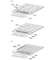
図1(A)に支持基板100上に設けられた単結晶半導体層を有する半導体素子層101a、101b、101cを示す。半導体素子層101a、101b、101cに含まれる単結晶半導体層は単結晶半導体基板より分離された単結晶半導体層である。
FIG. 1A illustrates
次に、支持基板100の厚さを研削、研磨処理によって薄くする工程を行う。工程時の支持基板100を固定する固定テープ103に半導体素子層101a、101b、101c側を向けて支持基板100を固定し、支持基板100を加工して、厚さの薄い支持基板102とする(図1(B)参照。)。支持基板100が厚さ0.5mmのガラス基板であるとすれば、支持基板102は、半分の0.25〜0.3mm程度に薄型化することが好ましい。支持基板の厚さを薄く加工することで、支持基板の分断にかかる工程時間の短縮、及び分断に用いるダイサーなど加工手段の摩耗を軽減することができる。研削処理及び研磨処理は好適に組み合わせて用いることができ、本実施の形態では、研削機により研削した後、研磨機により研磨処理で表面を平坦化する。研磨処理として化学的機械研磨を行ってもよい。
Next, a process of reducing the thickness of the
本発明は、支持基板を分断することによって、複数の半導体集積回路をチップ(或いは細長いスティック)状で取り出す。分断工程は、一度に行わず、まず、支持基板102に半導体素子層101a、101b、101cを分断するための溝106a、106b、106c、106dをダイサー104のダイシングブレードで形成する(図1(C)参照。)。支持基板105の溝106a、106b、106c、106dにおいて支持基板105は意図的に残存させる。残存させる支持基板105の厚さは、30μm〜50μm程度とすればよい。
In the present invention, a plurality of semiconductor integrated circuits are taken out in the form of chips (or elongated sticks) by dividing the support substrate. First,
次に、溝106a、106b、106c、106dの形成された支持基板105上に樹脂層107を形成する(図1(D)参照。)。樹脂層107は膜厚1μm〜20μmとすればよい。樹脂層の材料は、樹脂層形成後の工程において(例えば、半導体集積回路の実装時)加熱処理を用いる場合はその加熱温度に耐えうる樹脂材料を用いる。
Next, the
衝撃吸収材として機能する樹脂層を形成すると、半導体集積回路に、より耐ストレス性を付与することができる。例えば、本発明の樹脂層が設けられた半導体集積回路においては、約20Nの圧力を加えても破損することなく耐えることができる。 When a resin layer functioning as a shock absorbing material is formed, more stress resistance can be imparted to the semiconductor integrated circuit. For example, a semiconductor integrated circuit provided with the resin layer of the present invention can withstand without being damaged even when a pressure of about 20 N is applied.
樹脂層としては、ビニル樹脂、エポキシ樹脂、フェノール樹脂、ノボラック樹脂、アクリル樹脂、メラミン樹脂、ウレタン樹脂、シロキサン樹脂等の樹脂材料を用いることができる。樹脂層の作製方法はスピンコート法などの塗布法を用いることができ、その他液滴吐出法、印刷法、ディッピング法、ディスペンサ法、刷毛塗り法、スプレー法、フローコート法などを用いることもできる。 As the resin layer, a resin material such as a vinyl resin, an epoxy resin, a phenol resin, a novolac resin, an acrylic resin, a melamine resin, a urethane resin, or a siloxane resin can be used. As a method for producing the resin layer, a coating method such as a spin coating method can be used, and a droplet discharge method, a printing method, a dipping method, a dispenser method, a brush coating method, a spray method, a flow coating method, or the like can also be used. .
その後、樹脂層107及び支持基板105を溝106a、106b、106c、106dにおいて、切断して、複数の半導体集積回路に分断(分割)する。本実施の形態では、支持基板105及び樹脂層107を固定テープ111に固定し、支持基板105側より溝106a、106b、106c、106dに残存する支持基板105及び樹脂層107を、ダイサー108によって切断する。ダイサー108によって、支持基板105及び樹脂層107は分割され、支持基板109a、109b、109c、樹脂層110a、110b、110cとなる(図1(E)参照。)。本実施の形態では、固定テープ103、111として、ダイシングテープを用いる。
Thereafter, the
溝の形成された支持基板105及び樹脂層107を切断する際は、支持基板105側でも樹脂層107側からでも切断することができる。支持基板105にアライメント合わせのマーカーを形成する場合は、支持基板105側よりダイサー等の切断手段を用いて切断すると、切断箇所の正確性を高くすることができる。
When cutting the
以上の工程で、半導体集積回路112a、112b、112cを形成することができる(図1(F)参照。)。樹脂層107及び支持基板105を切断する切断面の幅を、溝の幅より狭くすることによって、支持基板側面に、溝に形成された樹脂層を残存させることができる。本実施の形態では、ダイサー104及びダイサー108の幅とは処理領域(ダイサーによって加工される領域)を決定するダイシングブレードの厚さとなる。
Through the above steps, the semiconductor integrated
溝の幅はダイサー104のダイシングブレードの幅a1に、切断面の幅は、ダイサー108のダイシングブレードの幅a2によって制御できるため、ダイサー104のダイシングブレードの幅a1よりダイサー108のダイシングブレードの幅a2を狭くすればよい。例えば、本実施の形態では、ダイサー104のダイシングブレードの幅a1を0.16mm、ダイサー108のダイシングブレードの幅a2を0.1mmとする。
Since the width of the groove can be controlled by the width a1 of the dicing blade of the
従って、半導体集積回路112a、112b、112cにおいて、半導体素子層101a、101b、101cの設けられていない面及び側面の一部は樹脂層110a、110b、110cで覆われる構造となる。
Therefore, in the semiconductor integrated
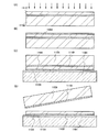
支持基板に形成される溝の形状は加工手段に依存する。本実施の形態ではダイサー104のやや丸みを帯びたダイシングブレードの形状が反映され、溝106a、106b、106c、106dも図1(C)の断面において丸み(曲率を有する)を帯びた形状となっている。ダイシングブレードの形状を矩形とすれば、溝の形状も矩形となり、分断後の半導体集積回路の支持基板の端部も矩形を有する形状とすることができる。
The shape of the groove formed in the support substrate depends on the processing means. In the present embodiment, the shape of the dicing blade having a slightly round shape of the
図18に矩形のダイシングブレードで加工する例を示す。図18(A)は、図1(B)と対応しており、半導体素子層101a、101b、101cが設けられた支持基板102は固定テープ103上で研削、研磨加工されている。
FIG. 18 shows an example of processing with a rectangular dicing blade. 18A corresponds to FIG. 1B, and the
支持基板102に半導体素子層101a、101b、101cを分断するための溝126a、126b、126c、126dをダイサー124で形成する(図18(B)参照。)。ダイサー124は矩形のダイシングブレードを用いるために、支持基板125の溝126a、126b、126c、126dは断面図において矩形となっている。
次に、溝126a、126b、126c、126dの形成された支持基板125上に樹脂層127を形成する(図18(C)参照。)。
Next, a
その後、樹脂層127及び支持基板125を溝126a、126b、126c、126dにおいて、切断して、複数の半導体集積回路に分断(分割)する。本実施の形態では、支持基板125及び樹脂層127を固定テープ131に固定し、支持基板125側より溝126a、126b、126c、126dに残存する支持基板125及び樹脂層127を、ダイサー128によって切断する。ダイサー128によって、支持基板125及び樹脂層127は分割され、支持基板129a、129b、129c、樹脂層130a、130b、130cとなる(図18(D)参照。)。
Thereafter, the
以上の工程で、半導体集積回路132a、132b、132cを形成することができる(図18(E)参照。)。半導体集積回路132a、132b、132cは矩形の形状の溝126a、126b、126c、126dの形状を反映し、断面図において側面に段差を有する形状となっている。
Through the above steps, the semiconductor integrated
また、基板の厚さは樹脂層と比較して厚いため、基板端部での被覆性を向上させるために、樹脂層も厚くすると好ましい。樹脂層を厚く形成するために積層構造としてもよい。樹脂層の構造や膜厚、また切断箇所によっても完成する半導体集積回路の形状を自由に変化させる(異ならせる)ことができる。図17に、樹脂層を積層する例を示す。 In addition, since the thickness of the substrate is thicker than that of the resin layer, it is preferable to increase the thickness of the resin layer in order to improve the coverage at the edge of the substrate. A laminated structure may be used in order to form the resin layer thick. The shape of the semiconductor integrated circuit to be completed can be freely changed (varied) depending on the structure and film thickness of the resin layer and the cutting location. FIG. 17 shows an example in which resin layers are stacked.
図17(A)は、図1(D)と対応しており、支持基板105の半導体素子層101a、101b、101cが設けられた反対面上に、樹脂層107が形成されている。次に樹脂層107上にさらに樹脂層を形成し、樹脂層113を形成する。本実施の形態では、樹脂層107と同材料の樹脂層を積層する(図17(B)参照。)。図1(E)と同様に固定テープ111を設けて固定した樹脂層113及び支持基板105を、ダイサー118によって分断し、支持基板109a、109b、109c、樹脂層114a、114b、114cとする(図17(C)参照。)。以上の工程で、形成される半導体集積回路115a、115b、115cは、図1(F)より樹脂層を厚く形成しているために、各半導体集積回路115a、115b、115cにおいて、支持基板109a、109b、109cと樹脂層114a、114b、114c端部とが一致する形状となる(図17(D)参照。)。
FIG. 17A corresponds to FIG. 1D, and the
ダイシングブレードの幅の細いダイサーを用いて分断すると、支持基板の溝の領域に、樹脂を、完成した半導体集積回路に多く残すこともできる。衝撃吸収材として機能する樹脂層を積層すると、半導体集積回路に、より耐ストレス性を付与することができる。 When the dicing blade is cut using a thin dicer, a large amount of resin can be left in the completed semiconductor integrated circuit in the groove region of the support substrate. When a resin layer that functions as a shock absorbing material is stacked, more stress resistance can be imparted to the semiconductor integrated circuit.
また、本発明では、溝を形成し、溝上に樹脂層を形成するので、溝底面に厚く樹脂層を形成することができる。さらに樹脂層を形成後、樹脂層と支持基板を積層して切断するため、側面において樹脂層の端部と支持基板の端部とが一致する。側面において支持基板の半導体素子層の形成面と反対側の端部が露出しないために、支持基板の端部の破損や欠けを防止することができる。また、樹脂層を積層により厚く形成すると、半導体集積回路の側面において支持基板の端部と樹脂層の端部との距離を長くすることができるため、より支持基板端部に与えるダメージを軽減することができる。 Moreover, in this invention, since a groove | channel is formed and a resin layer is formed on a groove | channel, a resin layer can be thickly formed in a groove | channel bottom face. Further, after the resin layer is formed, the resin layer and the support substrate are stacked and cut, so that the end of the resin layer and the end of the support substrate coincide with each other on the side surface. Since the end portion of the side surface of the support substrate opposite to the surface on which the semiconductor element layer is formed is not exposed, breakage or chipping of the end portion of the support substrate can be prevented. Further, when the resin layer is formed thickly by stacking, the distance between the end portion of the support substrate and the end portion of the resin layer can be increased on the side surface of the semiconductor integrated circuit, thereby further reducing damage to the end portion of the support substrate be able to.
半導体集積回路は、COG(Chip on Glass)方式や、TAB(Tape Automated Bonding)方式により、画素部が形成された絶縁表面を有する基板に実装することができる。本実施の形態で示すように、半導体集積回路において、樹脂層が半導体素子層側に露出しないために、はんだや異方性導電膜を用いて半導体集積回路を実装する際に行う加熱処理に対しても耐熱性を持たせることができる。 A semiconductor integrated circuit can be mounted on a substrate having an insulating surface on which a pixel portion is formed by a COG (Chip on Glass) method or a TAB (Tape Automated Bonding) method. As shown in this embodiment mode, in the semiconductor integrated circuit, since the resin layer is not exposed to the semiconductor element layer side, the heat treatment performed when mounting the semiconductor integrated circuit using solder or an anisotropic conductive film is used. However, heat resistance can be imparted.
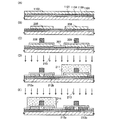
図2に固定テープ111に形成された半導体集積回路112aを画素部156が形成された絶縁表面を有する基板155にCOG方式で実装する例を示す。
FIG. 2 shows an example in which the semiconductor integrated
半導体集積回路112a、112b、112cにおいて薄く成形された支持基板109a、109b、109cは樹脂層110a、110b、110cで覆われているため工程上取扱い易く、破損などの不良が生じにくい。よって、より薄型の高性能な半導体装置を歩留まり良く作製することができる。
Since the
半導体集積回路112a、112b、112cにおいては、半導体素子層表面に実装時に電気的接続を行う端子として導電層が設けられている。
In the semiconductor integrated
例えば、スクリーン印刷法を用いて導電層を形成する場合には、粒径が数nmから数十μmの導電体粒子を有機樹脂に溶解または分散させた導電性のペーストを選択的に印刷することによって設けることができる。導電体粒子としては、銀(Ag)、金(Au)、銅(Cu)、ニッケル(Ni)、白金(Pt)、パラジウム(Pd)、タンタル(Ta)、モリブデン(Mo)およびチタン(Ti)等のいずれか一つ以上の金属粒子やハロゲン化銀の微粒子を用いることができる。また、導電性ペーストに含まれる有機樹脂は、金属粒子のバインダー、溶媒、分散剤および被覆材として機能する有機樹脂から選ばれた一つまたは複数を用いることができる。代表的には、エポキシ樹脂、シリコン樹脂等の有機樹脂が挙げられる。また、導電層の形成の際は、導電性のペーストを押し出した後に焼成することが好ましい。また、はんだや鉛フリーのはんだを主成分とする微粒子を用いてもよい。 For example, when a conductive layer is formed using a screen printing method, a conductive paste in which conductive particles having a particle size of several nanometers to several tens of micrometers are dissolved or dispersed in an organic resin is selectively printed. Can be provided. Conductor particles include silver (Ag), gold (Au), copper (Cu), nickel (Ni), platinum (Pt), palladium (Pd), tantalum (Ta), molybdenum (Mo) and titanium (Ti). Any one or more metal particles such as silver halide fine particles can be used. In addition, as the organic resin contained in the conductive paste, one or more selected from organic resins functioning as a binder of metal particles, a solvent, a dispersant, and a coating material can be used. Typically, an organic resin such as an epoxy resin or a silicon resin can be given. In forming the conductive layer, it is preferable to fire after extruding the conductive paste. Further, fine particles mainly composed of solder or lead-free solder may be used.
また、半導体集積回路と画素部に設けられた素子と電気的に接続されている配線との接続部分の構造としては、基板上の配線と半導体集積回路の電極に設けられた導電性の突起物であるバンプとを接触させ、基板と半導体集積回路間を樹脂で固定してもよい。また基板上の配線と半導体集積回路の電極端子の間に導電性の粒子を分散させた樹脂を設け、この導電性の粒子で半導体集積回路と基板上の配線との接続を行い、導電性の粒子を分散させた有機樹脂で接着、固定してもよい。また、接着に使用する樹脂としては光硬化性の樹脂や熱硬化性のものあるいは自然硬化性の樹脂等を用いることができる。 In addition, as a structure of a connection portion between the semiconductor integrated circuit and a wiring electrically connected to an element provided in the pixel portion, a conductive protrusion provided on the wiring on the substrate and the electrode of the semiconductor integrated circuit A bump may be contacted, and the substrate and the semiconductor integrated circuit may be fixed with resin. In addition, a resin in which conductive particles are dispersed is provided between the wiring on the substrate and the electrode terminal of the semiconductor integrated circuit, and the conductive particles are used to connect the semiconductor integrated circuit and the wiring on the substrate. You may adhere | attach and fix with the organic resin to which particle | grains were disperse | distributed. As the resin used for adhesion, a photo-curing resin, a thermosetting resin, a natural-curing resin, or the like can be used.
従来の半導体装置では、走査用、信号用にそれぞれ6〜10個ものドライバICを必要である。そのために半導体装置の周辺は多くの配線が複雑に形成されてしまう。しかしながら、本実施の形態で示した棒状のドライバーを装着することによって、半導体装置の周辺は非常にコンパクトになり、デザイン的にも洗練されたものになる。 A conventional semiconductor device requires 6 to 10 driver ICs for scanning and signals. Therefore, many wirings are complicatedly formed around the semiconductor device. However, by mounting the rod-shaped driver shown in this embodiment, the periphery of the semiconductor device becomes very compact and refined in design.
また、画素部が形成された絶縁表面を有する基板と、半導体集積回路の支持基板とは同じ材料を用いることができるので、その後の熱処理によっても熱膨張係数の違いから剥がれるなどの不良を防止することができる。さらに従来のドライバICは不透明で大きさに制限があったが、透光性のガラス基板を用いた半導体集積回路であれば、実質的に透明(回路部は不透明であるが、肉眼では判別できない。)であり、大きさも比較的自由に設定することができる。 In addition, since the same material can be used for the substrate having an insulating surface on which the pixel portion is formed and the supporting substrate of the semiconductor integrated circuit, defects such as peeling due to a difference in thermal expansion coefficient can be prevented by subsequent heat treatment. be able to. Furthermore, conventional driver ICs are opaque and limited in size. However, a semiconductor integrated circuit using a light-transmitting glass substrate is substantially transparent (the circuit portion is opaque, but cannot be identified with the naked eye). And the size can be set relatively freely.
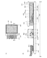
本発明の半導体装置において、半導体集積回路の他の実装例を図3に示す。 FIG. 3 shows another mounting example of the semiconductor integrated circuit in the semiconductor device of the present invention.
図3(A)に示すように、COG(Chip on Glass)方式によりドライバICである別途形成された半導体集積回路6013を、画素部6012が形成された基板6011上に実装しても良い。また他の実装形態として、図3(B)に示すようなTAB(Tape Automated Bonding)方式を用いて、半導体集積回路6023を、基板6021上に形成された画素部6022と電気的に接続するように実装してもよい。図3(A)乃至(C)において、半導体集積回路6013、6023、6033aは、FPC(Flexible printed Circuit)6015、6025、6035とそれぞれ接続している。なお、図では示されていないが半導体集積回路6033aと6033bは電気的に接続されている。
As shown in FIG. 3A, a separately formed semiconductor integrated
本発明の半導体集積回路は、自由に形状や設置領域を選択できるため、図3(A)のように短い複数の半導体集積回路6013を基板6011の1辺に隣接して設けてもよいし、図3(C)のように、基板6031の2辺に、1つずつ長い半導体集積回路6033a、6033bを設けてもよい。
Since the semiconductor integrated circuit of the present invention can freely select the shape and installation area, a plurality of short semiconductor
また、周辺駆動回路の一部を基板上に直接形成してもよい。例えば、走査線側駆動回路を基板上に形成し信号線側駆動回路を別途半導体集積回路として実装することもできる。 Further, a part of the peripheral driver circuit may be formed directly on the substrate. For example, the scanning line side driving circuit can be formed over a substrate and the signal line side driving circuit can be separately mounted as a semiconductor integrated circuit.
半導体集積回路が有する半導体素子には単結晶半導体基板より分離された単結晶半導体層を用いている。さらに半導体集積回路が設けられた薄く成形された基板は樹脂層で覆われているため工程上取扱い易く、破損などの不良が生じにくい。よって、より薄型の高性能な半導体装置を歩留まり良く作製することができる。 A semiconductor element included in a semiconductor integrated circuit uses a single crystal semiconductor layer separated from a single crystal semiconductor substrate. Further, a thinly molded substrate provided with a semiconductor integrated circuit is covered with a resin layer, so that it is easy to handle in the process and hardly causes defects such as breakage. Accordingly, a thinner high-performance semiconductor device can be manufactured with high yield.
なお、別途形成した基板の接続方法は、特に限定されるものではなく、COG方法、ワイヤボンディング方法、或いはTAB方法などを用いることができる。また接続する位置は、電気的な接続が可能であるならば、図3に示した位置に限定されない。また、コントローラ、CPU、メモリ等を別途形成し、接続するようにしても良い。 Note that a method for connecting a separately formed substrate is not particularly limited, and a COG method, a wire bonding method, a TAB method, or the like can be used. Further, the connection position is not limited to the position illustrated in FIG. 3 as long as electrical connection is possible. In addition, a controller, a CPU, a memory, and the like may be separately formed and connected.
なお本発明で用いる半導体集積回路が形成する回路は、シフトレジスタとアナログスイッチのみを有する形態に限定されない。シフトレジスタとアナログスイッチに加え、バッファ、レベルシフタ、ソースフォロワ等、他の回路を有していても良い。また、シフトレジスタとアナログスイッチは必ずしも設ける必要はなく、例えばシフトレジスタの代わりにデコーダ回路のような信号線の選択ができる別の回路を用いても良いし、アナログスイッチの代わりにラッチ等を用いても良い。 Note that a circuit formed by a semiconductor integrated circuit used in the present invention is not limited to a mode having only a shift register and an analog switch. In addition to the shift register and the analog switch, other circuits such as a buffer, a level shifter, and a source follower may be included. The shift register and the analog switch are not necessarily provided. For example, another circuit that can select a signal line such as a decoder circuit may be used instead of the shift register, or a latch or the like may be used instead of the analog switch. May be.
本発明において、半導体集積回路が駆動回路(ドライバー)として実装される表示機能を有する半導体装置は、パッシブマトリクス型でもアクティブマトリクス型でもよい。さらに、半導体駆動回路は、メモリ素子の駆動回路として実装し、メモリ機能を有する半導体装置を作製することもできる。 In the present invention, a semiconductor device having a display function in which a semiconductor integrated circuit is mounted as a driver circuit (driver) may be a passive matrix type or an active matrix type. Further, the semiconductor drive circuit can be mounted as a drive circuit for a memory element to manufacture a semiconductor device having a memory function.
また、本発明において画素部が設けられる基板に直接形成されるトランジスタの有する半導体層は、非晶質半導体、微結晶半導体、多結晶半導体などを用いることができる。 In the present invention, an amorphous semiconductor, a microcrystalline semiconductor, a polycrystalline semiconductor, or the like can be used for a semiconductor layer included in a transistor directly formed over a substrate provided with a pixel portion.
以下、絶縁表面を有する基板である支持基板上に、単結晶半導体基板より単結晶半導体層を設け、半導体集積回路に含まれる半導体素子を形成する方法を図4及び図5を用いて説明する。 Hereinafter, a method for forming a semiconductor element included in a semiconductor integrated circuit by providing a single crystal semiconductor layer from a single crystal semiconductor substrate over a supporting substrate which is a substrate having an insulating surface will be described with reference to FIGS.
図4(A)に示す単結晶半導体基板1108は清浄化されており、その表面から電界で加速されたイオンを所定の深さに添加し、脆弱化層1110を形成する。イオンの添加は支持基板に転置する単結晶半導体層の厚さを考慮して行われる。イオンを添加する際の加速電圧はこのような厚さを考慮して、単結晶半導体基板1108に添加されるようにする。本発明では、単結晶半導体基板へイオンを添加し、イオンにより微小な空洞を有するように脆弱化された領域を脆弱化層という。
A single
単結晶半導体基板1108には、市販の単結晶半導体基板を用いることができ、例えば、単結晶シリコン基板、単結晶ゲルマニウム基板、単結晶シリコンゲルマニウム基板など、第4族元素でなる単結晶半導体基板を用いることができる。また、ガリウムヒ素やインジウムリン等の化合物半導体基板も用いることができる。半導体基板として多結晶半導体基板を用いてもよい。もちろん、単結晶半導体基板は、円形のウエハに限定されるものではなく、様々な形状の単結晶半導体基板を用いることができる。例えば、長方形、五角形、六角形などの多角形の基板を用いることができる。もちろん、市販の円形状の単結晶半導体ウエハを単結晶半導体基板に用いることも可能である。円形状の単結晶半導体ウエハには、シリコンやゲルマニウムなどの半導体ウエハ、ガリウムヒ素やインジウムリンなどの化合物半導体ウエハなどがある。単結晶半導体ウエハの代表例は、単結晶シリコンウエハであり、直径5インチ(125mm)、直径6インチ(150mm)、直径8インチ(200mm)、直径12インチ(300mm)サイズ、直径400mm、直径450mmの円形のウエハを用いることができる。また、長方形の単結晶半導体基板は、市販の円形状の単結晶半導体ウエハを切断することで形成することができる。基板の切断には、ダイサー或いはワイヤソー等の切断装置、レーザ切断、プラズマ切断、電子ビーム切断、その他任意の切断手段を用いることができる。また、基板として薄片化する前の半導体基板製造用のインゴットを、その断面が長方形になるように直方体状に加工し、この直方体状のインゴットを薄片化することでも、長方形状の単結晶半導体基板を製造することができる。また、単結晶半導体基板の厚さは特に限定されないが、単結晶半導体基板を再利用することを考慮すれば、厚い方が1枚の原料ウエハからより多くの単結晶半導体層を形成することができるため、好ましい。市場に流通している単結晶シリコンウエハの厚さは、そのサイズはSEMI規格に準じており、例えば直径6インチのウエハは膜厚625μm、直径8インチのウエハは膜厚725μm、直径12インチのウエハは775μmとされている。なお、SEMI規格のウエハの厚さは公差±25μmを含んでいる。もちろん、原料となる単結晶半導体基板の厚さはSEMI規格に限定されず、インゴットをスライスするときに、その厚さを適宜調節することができる。もちろん、再利用された単結晶半導体基板1108を用いるときには、その厚さは、SEMI規格よりも薄くなる。支持基板上に得られる単結晶半導体層は母体となる半導体基板を選択することによって決定することができる。
As the single
また、単結晶半導体基板1108は、作製する半導体素子(本実施の形態においては電界効果トランジスタ)によって、結晶面方位を選択すればよい。例えば、結晶面方位として{100}面、{110}面など有する単結晶半導体基板を用いることができる。
Further, the crystal plane orientation of the single
本実施の形態は、単結晶半導体基板の所定の深さに水素、ヘリウム、又はフッ素をイオン添加し、その後熱処理を行って表層の単結晶半導体層を剥離するイオン添加剥離法で形成するが、ポーラスシリコン上に単結晶シリコンをエピタキシャル成長させた後、ポーラスシリコン層をウオータージェットで劈開して剥離する方法を適用しても良い。 In this embodiment mode, hydrogen, helium, or fluorine is ion-added to a predetermined depth of the single crystal semiconductor substrate, and then heat treatment is performed to form the surface single crystal semiconductor layer, which is formed by an ion addition peeling method. A method may be applied in which single crystal silicon is epitaxially grown on porous silicon, and then the porous silicon layer is cleaved with a water jet and peeled off.
単結晶半導体基板1108として単結晶シリコン基板を用い、希フッ酸で表面を処理し、自然酸化膜の除去と表面に付着するゴミ等の汚染物も除去して単結晶半導体基板1108表面を清浄化する。
A single crystal silicon substrate is used as the single
脆弱化層1110は、イオンをイオンドーピング法(ID法と略記する)やイオン注入法(II法と略記する)によって添加(導入)すればよい。脆弱化層1110は水素、ヘリウム若しくはフッ素に代表されるハロゲンのイオンを添加することで形成される。ハロゲン元素としてフッ素イオンを添加する場合にはソースガスとしてBF3を用いれば良い。なお、イオン注入とはイオン化したガスを質量分離して半導体に添加する方式をいう。
The
例えば、イオン注入法を用いて、イオン化した水素ガスを質量分離し、H+のみ、(又はH2 +のみ)を選択的に加速して添加することができる。 For example, ionized hydrogen gas can be mass-separated using an ion implantation method, and H + alone (or H 2 + alone) can be selectively accelerated and added.
イオンドープ法は、イオン化したガスを質量分離せずに、プラズマ中で複数種のイオン種を作り、それらを加速して単結晶半導体基板にドープする。例えば、H+、H2 +、H3 +イオンを含む水素では、ドープされるイオンは、代表的にH3 +イオンが50%以上、例えばH3 +イオンが80%、他のイオン(H+、H2 +イオン)が20%、が一般的である。H3 +イオンのイオン種のみとして添加することもここではイオンドープとする。 In the ion doping method, a plurality of types of ion species are generated in plasma without mass separation of ionized gas, and they are accelerated to dope a single crystal semiconductor substrate. For example, H +, H 2 +, the hydrogen containing H 3 + ions, ions to be doped is typically H 3 + ions is 50% or more, for example H 3 + ions is 80%, other ions (H + , H 2 + ion) is typically 20%. Here, adding only as an ion species of H 3 + ions is also referred to as ion doping.
また、一又は複数の同一の原子から成る質量の異なるイオンを添加してもよい。例えば、水素イオンを添加する場合には、H+、H2 +、H3 +イオンを含ませると共に、H3 +イオンの割合を高めておくことが好ましい。水素イオンを添加する場合には、H+、H2 +、H3 +イオンを含ませると共に、H3 +イオンの割合を高めておくと添加効率を高めることができ、添加時間を短縮することができる。このような構成とすることで、剥離を容易に行うことができる。 In addition, ions having different masses composed of one or a plurality of the same atoms may be added. For example, when hydrogen ions are added, it is preferable to include H + , H 2 + , and H 3 + ions and to increase the ratio of H 3 + ions. When hydrogen ions are added, H + , H 2 + , H 3 + ions are included, and if the ratio of H 3 + ions is increased, the addition efficiency can be increased and the addition time can be shortened. Can do. With such a configuration, peeling can be easily performed.
以下、イオンドーピング法とイオン注入法について詳細に説明する。イオンドーピング法に用いるイオンドーピング装置(ID装置ともいう)では、プラズマ空間が大きく、大量のイオンを単結晶半導体基板に添加することができる。一方、イオン注入法に用いるイオン注入装置(II装置ともいう)は、プラズマから取り出したイオンを質量分析して特定のイオン種だけを半導体基板に打ち込めるという特徴があり、基本的に点ビ−ムをスキャンさせて処理する。 Hereinafter, the ion doping method and the ion implantation method will be described in detail. In an ion doping apparatus (also referred to as an ID apparatus) used for an ion doping method, a plasma space is large and a large amount of ions can be added to a single crystal semiconductor substrate. On the other hand, an ion implantation apparatus (also referred to as an II apparatus) used for the ion implantation method is characterized by mass-analyzing ions extracted from plasma and implanting only specific ion species into a semiconductor substrate. Scan and process.
プラズマ発生方法としては、どちらの装置も、例えば、フィラメントを熱して出てくる熱電子によりプラズマ状態を作っている。しかし、生成される水素イオン(H+、H2 +、H3 +)が半導体基板に添加される(打ち込まれる)際の水素イオン種の割合は、イオンドーピング法とイオン注入法で大きく異なる。 As a plasma generation method, both apparatuses create a plasma state by, for example, thermoelectrons that are generated by heating a filament. However, the ratio of the hydrogen ion species when the generated hydrogen ions (H + , H 2 + , H 3 + ) are added (implanted) to the semiconductor substrate is greatly different between the ion doping method and the ion implantation method.
H3 +をより多く打ち込むという観点からすれば、イオン注入装置よりイオンドーピング装置を用いる方が好ましいといえる。 From the viewpoint of implanting more H 3 + , it can be said that it is preferable to use an ion doping apparatus rather than an ion implantation apparatus.
単結晶シリコン基板に水素イオンやフッ素イオンのようなハロゲンイオンを添加した場合、添加されたフッ素等が、シリコン結晶格子内のシリコン原子をノックアウトする(追い出す)ことによって空白部分を効果的に作り出し、脆弱化層に微小な空洞を作る。この場合、比較的低温の熱処理によって脆弱化層に形成された微小な空洞の体積変化が起こり、脆弱化層に沿って劈開することにより薄い単結晶半導体層を形成することができる。フッ素イオンを添加した後に、水素イオンを添加して空洞内に水素を含ませるようにしても良い。単結晶半導体基板から薄い単結晶半導体層を剥離するために形成する脆弱化層は、脆弱化層に形成された微小な空洞の体積変化を利用して劈開をするので、このようにフッ素イオンや水素イオンの作用を有効利用することが好ましい。 When halogen ions such as hydrogen ions and fluorine ions are added to a single crystal silicon substrate, the added fluorine or the like effectively creates a blank portion by knocking out (displacing) silicon atoms in the silicon crystal lattice, Create a small cavity in the weakened layer. In this case, a volume change of a minute cavity formed in the weakened layer occurs by heat treatment at a relatively low temperature, and a thin single crystal semiconductor layer can be formed by cleaving along the weakened layer. After adding fluorine ions, hydrogen ions may be added so that the cavities contain hydrogen. The weakening layer formed to peel the thin single crystal semiconductor layer from the single crystal semiconductor substrate is cleaved by utilizing the volume change of a minute cavity formed in the weakening layer. It is preferable to effectively use the action of hydrogen ions.
また、単結晶半導体基板と上記単結晶半導体層と接合する絶縁層との間に、保護層を形成してもよい。保護層は、窒化シリコン層、酸化シリコン層、窒化酸化シリコン層、又は酸化窒化シリコン層から選ばれた一層又は複数の層による積層構造により形成することができる。これらの層は、単結晶半導体基板に脆弱化層が形成される前に単結晶半導体基板上に形成することができる。また、単結晶半導体基板に脆弱化層を形成した後に単結晶半導体基板上に形成してもよい。 Further, a protective layer may be formed between the single crystal semiconductor substrate and the insulating layer bonded to the single crystal semiconductor layer. The protective layer can be formed by a single layer or a stacked layer structure including a plurality of layers selected from a silicon nitride layer, a silicon oxide layer, a silicon nitride oxide layer, and a silicon oxynitride layer. These layers can be formed over the single crystal semiconductor substrate before the weakening layer is formed over the single crystal semiconductor substrate. Alternatively, the weakening layer may be formed over the single crystal semiconductor substrate and then formed over the single crystal semiconductor substrate.
脆弱化層の形成に当たってはイオンを高ドーズ条件で添加する必要があり、単結晶半導体基板1108の表面が粗くなってしまう場合がある。そのためイオンが添加される表面に窒化シリコン膜、窒化酸化シリコン膜、若しくは酸化シリコン膜などによりイオン添加に対する保護層を50nm乃至200nmの厚さで設けておいても良い。
In forming the weakened layer, ions must be added under a high dose condition, and the surface of the single
例えば、単結晶半導体基板1108上に保護層としてプラズマCVD法により酸化窒化シリコン膜(膜厚5nm〜300nm、望ましくは30nm〜150nm(例えば50nm))と窒化酸化シリコン膜(膜厚5nm〜150nm、望ましくは10nm〜100nm(例えば50nm))の積層を形成する。一例としては、単結晶半導体基板1108上に酸化窒化シリコン膜を膜厚50nm形成し、該酸化窒化シリコン膜上に窒化酸化シリコン膜を膜厚50nm形成し、積層する。酸化窒化シリコン膜は有機シランガスを用いて化学気相成長法により作製される酸化シリコン膜でもよい。
For example, a silicon oxynitride film (film thickness: 5 nm to 300 nm, desirably 30 nm to 150 nm (eg, 50 nm)) and a silicon nitride oxide film (film thickness: 5 nm to 150 nm, desirably, as a protective layer over the single
また、単結晶半導体基板1108を脱脂洗浄し、表面の酸化膜を除去して熱酸化を行ってもよい。熱酸化としては通常のドライ酸化でも良いが、酸化雰囲気中にハロゲンを添加した酸化を行うことが好ましい。例えば、酸素に対しHClを0.5〜10体積%(好ましくは3体積%)の割合で含む雰囲気中で、700℃以上の温度で熱処理を行う。好適には950℃〜1100℃の温度で熱酸化を行うと良い。処理時間は0.1〜6時間、好ましくは0.5〜3.5時間とすれば良い。形成される酸化膜の膜厚としては、10nm〜1000nm(好ましくは50nm〜200nm)、例えば100nmの厚さとする。
Alternatively, the single
ハロゲンを含むものとしてはHClの他に、HF、NF3、HBr、Cl2、ClF3、BCl3、F2、Br2などから選ばれた一種又は複数種を適用することができる。 In addition to HCl, one or more selected from HF, NF 3 , HBr, Cl 2 , ClF 3 , BCl 3 , F 2 , Br 2 and the like can be used as the halogen-containing material.
このような温度範囲で熱処理を行うことで、ハロゲン元素によるゲッタリング効果を得ることができる。ゲッタリングとしては、特に金属不純物を除去する効果がある。すなわち、塩素の作用により、金属などの不純物が揮発性の塩化物となって気相中へ離脱して除去される。単結晶半導体基板1108の表面を化学的機械研磨(CMP)処理をしたものに対しては有効である。また、水素は単結晶半導体基板1108と形成される絶縁層との界面の欠陥を補償して界面の局在準位密度を低減する作用を奏し、単結晶半導体基板1108と絶縁層との界面が不活性化されて電気的特性が安定化する。
By performing heat treatment in such a temperature range, a gettering effect by a halogen element can be obtained. Gettering is particularly effective in removing metal impurities. That is, by the action of chlorine, impurities such as metals become volatile chlorides and are released into the gas phase and removed. This is effective for the surface of the single
この熱処理により形成される酸化膜中にハロゲンを含ませることができる。ハロゲン元素は1×10¹⁷atoms/cm3〜5×1020atoms/cm3の濃度で含まれることにより金属などの不純物を捕獲して単結晶半導体基板1108の汚染を防止する保護層としての機能を発現させることができる。
Halogen can be contained in the oxide film formed by this heat treatment. Since the halogen element is contained at a concentration of 1 × 10 17 atoms / cm 3 to 5 × 10 20 atoms / cm 3 , it functions as a protective layer that captures impurities such as metals and prevents contamination of the single
脆弱化層1110を形成する際、加速電圧と全イオン数は、単結晶半導体基板上に堆積した膜の厚さと、目的とする単結晶半導体基板より分離して支持基板上に転置される単結晶半導体層の膜厚と、添加するイオン種によって調整することができる。
When the
例えば、イオンドーピング法で原料として水素ガスを用い、加速電圧を40kV、全イオン数2×10¹⁶ions/cm2でイオンを添加して脆弱化層を形成することができる。保護層の膜厚を厚くすれば、同一条件でイオンを添加し脆弱化層を形成した場合、目的とする単結晶半導体基板より分離して支持基板上に転置(転載)される単結晶半導体層として、膜厚の薄い単結晶半導体層を形成することができる。例えば、イオン種(H+、H2 +、H3 +イオン)の割合にもよるが、上記条件で脆弱化層を形成するとし、保護層として単結晶半導体基板上に酸化窒化シリコン膜(膜厚50nm)と窒化酸化シリコン膜(膜厚50nm)を保護層として積層する場合、支持基板に転置される単結晶半導体層の膜厚は約120nmとなり、単結晶半導体基板上に酸化窒化シリコン膜(膜厚100nm)と窒化酸化シリコン膜(膜厚50nm)を保護層として積層する場合は、支持基板に転置される単結晶半導体層の膜厚は約70nmとなる。 For example, the weakened layer can be formed by using hydrogen gas as a raw material in the ion doping method, adding ions at an acceleration voltage of 40 kV, and a total number of ions of 2 × 10 16 ions / cm 2 . If the thickness of the protective layer is increased, when a weakened layer is formed by adding ions under the same conditions, the single crystal semiconductor layer separated from the target single crystal semiconductor substrate and transferred (transferred) onto the support substrate As described above, a thin single crystal semiconductor layer can be formed. For example, although depending on the ratio of ion species (H + , H 2 + , H 3 + ions), a weakened layer is formed under the above conditions, and a silicon oxynitride film (film) is formed on the single crystal semiconductor substrate as a protective layer. When a protective layer is formed by stacking a silicon nitride oxide film (thickness 50 nm) and a silicon nitride oxide film (film thickness 50 nm), the thickness of the single crystal semiconductor layer transferred to the supporting substrate is approximately 120 nm, and a silicon oxynitride film ( In the case where a film thickness of 100 nm) and a silicon nitride oxide film (film thickness of 50 nm) are stacked as a protective layer, the thickness of the single crystal semiconductor layer transferred to the supporting substrate is approximately 70 nm.
ヘリウム(He)や水素を原料ガスにする場合、加速電圧を10kV〜200kVの範囲で、ドーズ量を1×10¹⁶ions/cm2〜6×1016ions/cm2の範囲で添加し脆弱化層を形成することができる。ヘリウムを原料ガスにすると、質量分離を行わなくてもHe+イオンを主なイオンとして添加することができる。また、水素を原料ガスとするとH3 +イオンやH2 +イオンを主なイオンとして添加することができる。イオン種は、プラズマの生成方法、圧力、原料ガス供給量、加速電圧によっても変化する。 When helium (He) or hydrogen is used as a source gas, it is weakened by adding an acceleration voltage in the range of 10 kV to 200 kV and a dose amount in the range of 1 × 10 16 ions / cm 2 to 6 × 10 16 ions / cm 2 . A layer can be formed. When helium is used as a source gas, He + ions can be added as main ions without mass separation. In addition, when hydrogen is used as a source gas, H 3 + ions and H 2 + ions can be added as main ions. The ion species also varies depending on the plasma generation method, pressure, source gas supply amount, and acceleration voltage.
脆弱化層形成の例としては、単結晶半導体基板上に酸化窒化シリコン膜(膜厚50nm)、窒化酸化シリコン膜(膜厚50nm)、及び酸化シリコン膜(膜厚50nm)を保護層として積層し、水素を加速電圧40kV、ドーズ量2×10¹⁶ions/cm2で添加し単結晶半導体基板に脆弱化層を形成する。その後保護層の最上層である該酸化シリコン膜上に接合面を有する絶縁層として酸化シリコン膜(膜厚50nm)を形成する。脆弱化層形成の他の例としては、単結晶半導体基板上に酸化シリコン膜(膜厚100nm)、及び窒化酸化シリコン膜(膜厚50nm)を保護層として積層し、水素を加速電圧40kV、ドーズ量2×1016ions/cm2で添加し単結晶半導体基板に脆弱化層を形成する。その後保護層の最上層である該窒化酸化シリコン膜上に接合面を有する絶縁層として酸化シリコン膜(膜厚50nm)を形成する。なお、上記酸化窒化シリコン膜及び窒化酸化シリコン膜はプラズマCVD法により形成すればよく、上記酸化シリコン膜は有機シランガスを用いてCVD法により形成すればよい。 As an example of forming a weakened layer, a silicon oxynitride film (film thickness 50 nm), a silicon nitride oxide film (film thickness 50 nm), and a silicon oxide film (film thickness 50 nm) are stacked as a protective layer over a single crystal semiconductor substrate. Hydrogen is added at an acceleration voltage of 40 kV and a dose of 2 × 10 16 ions / cm 2 to form a weakened layer on the single crystal semiconductor substrate. Thereafter, a silicon oxide film (film thickness: 50 nm) is formed as an insulating layer having a bonding surface over the silicon oxide film which is the uppermost layer of the protective layer. As another example of forming the weakened layer, a silicon oxide film (film thickness: 100 nm) and a silicon nitride oxide film (film thickness: 50 nm) are stacked over a single crystal semiconductor substrate as a protective layer, and hydrogen is accelerated at a voltage of 40 kV and a dose. An amount of 2 × 10 16 ions / cm 2 is added to form a weakened layer on the single crystal semiconductor substrate. After that, a silicon oxide film (film thickness: 50 nm) is formed as an insulating layer having a bonding surface over the silicon nitride oxide film which is the uppermost layer of the protective layer. Note that the silicon oxynitride film and the silicon nitride oxide film may be formed by a plasma CVD method, and the silicon oxide film may be formed by a CVD method using an organosilane gas.
また、支持基板と単結晶半導体基板との間に絶縁層を形成してもよい。絶縁層は支持基板側、あるいは単結晶半導体基板側どちらか一方でもよいし、両方に形成してもよい。接合を形成する面に形成する絶縁層は平滑面を有し親水性表面を形成する。該絶縁層としては、酸化シリコン膜を用いることができる。酸化シリコン膜としては有機シランガスを用いて化学気相成長法により作製される酸化シリコン膜が好ましい。その他に、シランガスを用いて化学気相成長法により作製される酸化シリコン膜を適用することもできる。 An insulating layer may be formed between the supporting substrate and the single crystal semiconductor substrate. The insulating layer may be formed on either the supporting substrate side, the single crystal semiconductor substrate side, or both. The insulating layer formed on the surface where the bond is formed has a smooth surface and forms a hydrophilic surface. As the insulating layer, a silicon oxide film can be used. As the silicon oxide film, a silicon oxide film formed by a chemical vapor deposition method using an organosilane gas is preferable. In addition, a silicon oxide film manufactured by a chemical vapor deposition method using silane gas can be used.
有機シランガスとしては、珪酸エチル(TEOS:化学式Si(OC2H5)4)、トリメチルシラン(TMS:(CH3)3SiH)、テトラメチルシラン(化学式Si(CH3)4)、テトラメチルシクロテトラシロキサン(TMCTS)、オクタメチルシクロテトラシロキサン(OMCTS)、ヘキサメチルジシラザン(HMDS)、トリエトキシシラン(SiH(OC2H5)3)、トリスジメチルアミノシラン(SiH(N(CH3)2)3)等のシリコン含有化合物を用いることができる。なお、原料ガスに有機シランを用いて化学気相成長法により酸化シリコン層を形成する場合、酸素を付与するガスを混合させることが好ましい。酸素を付与するガスとしては、酸素、亜酸化窒素、二酸化窒素等を用いることができる。さらに、アルゴン、ヘリウム、窒素又は水素等の不活性ガスを混合させてもよい。 Examples of the organic silane gas include ethyl silicate (TEOS: chemical formula Si (OC 2 H 5 ) 4 ), trimethylsilane (TMS: (CH 3 ) 3 SiH), tetramethylsilane (chemical formula Si (CH 3 ) 4 ), tetramethylcyclo Tetrasiloxane (TMCTS), octamethylcyclotetrasiloxane (OMCTS), hexamethyldisilazane (HMDS), triethoxysilane (SiH (OC 2 H 5 ) 3 ), trisdimethylaminosilane (SiH (N (CH 3 ) 2 ) 3 ) and other silicon-containing compounds can be used. Note that in the case where a silicon oxide layer is formed by a chemical vapor deposition method using organosilane as a source gas, it is preferable to mix an oxygen-providing gas. As a gas for imparting oxygen, oxygen, nitrous oxide, nitrogen dioxide, or the like can be used. Further, an inert gas such as argon, helium, nitrogen or hydrogen may be mixed.
また、接合を形成する面に形成する絶縁層として、モノシラン、ジシラン、又はトリシラン等のシランを原料ガスに用いて化学気相成長法により形成される酸化シリコン膜を適用することもできる。この場合も、酸素を付与するガスや不活性ガス等を混合させることが好ましい。また、単結晶半導体層と接合する絶縁層となる酸化シリコン膜は、塩素を含んでいてもよい。なお、本明細書において、化学気相成長(CVD;Chemical Vapor Deposition)法は、プラズマCVD法、熱CVD法、光CVD法を範疇に含む。 Alternatively, a silicon oxide film formed by a chemical vapor deposition method using silane such as monosilane, disilane, or trisilane as a source gas can be used as an insulating layer formed on a surface where a bond is formed. Also in this case, it is preferable to mix an oxygen-providing gas, an inert gas, or the like. Further, the silicon oxide film to be an insulating layer bonded to the single crystal semiconductor layer may contain chlorine. Note that in this specification, a chemical vapor deposition (CVD) method includes, in its category, a plasma CVD method, a thermal CVD method, and a photo CVD method.
その他、接合を形成する面に形成する絶縁層として、酸化性雰囲気下において熱処理することにより形成される酸化シリコン、酸素ラジカルの反応により成長する酸化シリコン、酸化性の薬液により形成されるケミカルオキサイドなどを適用することもできる。絶縁層として、シロキサン(Si−O−Si)結合を含む絶縁層を適用してもよい。また、前記有機シランガスと、酸素ラジカル又は窒素ラジカルとを反応させて絶縁層を形成してもよい。 In addition, as an insulating layer formed on the surface to form a bond, silicon oxide formed by heat treatment in an oxidizing atmosphere, silicon oxide grown by reaction of oxygen radicals, chemical oxide formed by an oxidizing chemical, etc. Can also be applied. An insulating layer containing a siloxane (Si—O—Si) bond may be used as the insulating layer. Further, the insulating layer may be formed by reacting the organic silane gas with oxygen radicals or nitrogen radicals.
絶縁層において、接合を形成する面の表面は、算術平均粗さRaが0.8nm未満、二乗平均平方根粗さRmsが0.9nm未満が望ましく、Raが0.4nm以下、Rmsが0.5nm以下がより望ましく、さらにはRaが0.3nm以下、Rmsが0.4nm以下がより望ましい。例えば、Raが0.27nm、Rmsが0.34nmである。本明細書においてRaは算術平均粗さであり、Rmsは二乗平均平方根粗さであり、測定範囲は2μm2、又は10μm2である。 In the insulating layer, the surface of the surface where the junction is formed preferably has an arithmetic average roughness Ra of less than 0.8 nm, a root mean square roughness Rms of less than 0.9 nm, an Ra of 0.4 nm or less, and an Rms of 0.5 nm. More preferably, Ra is 0.3 nm or less, and Rms is 0.4 nm or less. For example, Ra is 0.27 nm and Rms is 0.34 nm. In this specification, Ra is the arithmetic mean roughness, Rms is the root mean square roughness, and the measurement range is 2 μm 2 or 10 μm 2 .
支持基板と単結晶半導体基板とを接合するに際し、接合を形成する面の一方若しくは双方に、好ましくは有機シランを原材料として成膜した酸化シリコン膜でなる絶縁層を設けると強固な接合を形成することができる。 When the support substrate and the single crystal semiconductor substrate are bonded to each other, a strong bond is formed by providing an insulating layer made of a silicon oxide film, preferably formed using organosilane as a raw material, on one or both surfaces of the bond. be able to.
本実施の形態では、図4(B)で示すように支持基板と接合を形成する面に絶縁層1104として酸化シリコン膜を形成する。酸化シリコン膜としては有機シランガスを用いて化学気相成長法により作製される酸化シリコン膜が好ましい。その他に、シランガスを用いて化学気相成長法により作製される酸化シリコン膜を適用することもできる。化学気相成長法による成膜では、単結晶半導体基板に形成した脆弱化層1110から脱ガスが起こらない温度として、例えば350℃以下(具体的な例としては300℃)の成膜温度が適用される。また、単結晶半導体基板から単結晶半導体層を剥離する熱処理は、成膜温度よりも高い熱処理温度が適用される。
In this embodiment mode, as illustrated in FIG. 4B, a silicon oxide film is formed as the insulating
支持基板には、不純物元素の拡散を防止する窒化シリコン膜又は窒化酸化シリコン膜をブロッキング層(バリア層ともいう)として設けてもよい。さらに応力を緩和する作用のある絶縁膜として酸化窒化シリコン膜を組み合わせても良い。 The supporting substrate may be provided with a silicon nitride film or a silicon nitride oxide film which prevents diffusion of an impurity element as a blocking layer (also referred to as a barrier layer). Further, a silicon oxynitride film may be combined as an insulating film having a function of relieving stress.
図4(C)は支持基板1101上に設けられたブロッキング層1109と単結晶半導体基板1108の絶縁層1104が形成された面とを密接させ、この両者を接合させる態様を示す。接合を形成する面は、十分に清浄化しておく。支持基板1101上に設けられたブロッキング層1109と単結晶半導体基板1108の絶縁層1104が形成された面は、メガソニック洗浄などによって清浄化すればよい。また、メガソニック洗浄後にオゾン水で洗浄し、有機物の除去と表面の親水性向上を行ってもよい。
FIG. 4C illustrates a mode in which the
支持基板1101上のブロッキング層1109と絶縁層1104とを対向させて、一箇所を外部から押しつけると、局所的に接合面同士の距離が縮まる事によるファン・デル・ワールス力の強まりや水素結合の寄与によって、お互いに引きつけ合う。更に、隣接した領域でも対向する支持基板1101上のブロッキング層1109と絶縁層1104との間の距離が縮まるので、ファン・デル・ワールス力が強く作用する領域や水素結合が関与する領域が広がる事によって、接合(ボンディングともいう)が進行し接合面全域に接合が広がる。例えば、押しつける圧力は、100kPa〜5000kPa程度とすればよい。また、支持基板と半導体基板とを重ねるように配置し、重ねる基板の重みでも接合を広げることもできる。
When the
良好な接合を形成するために、表面を活性化しておいても良い。例えば、接合を形成する面に原子ビーム若しくはイオンビームを照射する。原子ビーム若しくはイオンビームを利用する場合には、アルゴン等の不活性ガス中性原子ビーム若しくは不活性ガスイオンビームを用いることができる。その他に、プラズマ照射若しくはラジカル処理を行う。このような表面処理により200℃乃至400℃の温度であっても異種材料間の接合を形成することが容易となる。 In order to form a good bond, the surface may be activated. For example, an atomic beam or an ion beam is irradiated to the surface on which the junction is formed. When an atomic beam or an ion beam is used, an inert gas neutral atom beam or inert gas ion beam such as argon can be used. In addition, plasma irradiation or radical treatment is performed. Such surface treatment makes it easy to form a bond between different materials even at a temperature of 200 ° C. to 400 ° C.
また、支持基板と絶縁層との接合界面の接合強度を向上させるために、加熱処理を行うと好ましい。例えば、オーブンや炉などで70℃〜350℃(例えば200℃で2時間)の温度条件で熱処理を行う。 In addition, heat treatment is preferably performed in order to improve the bonding strength at the bonding interface between the support substrate and the insulating layer. For example, heat treatment is performed in a temperature condition of 70 ° C. to 350 ° C. (for example, 200 ° C. for 2 hours) in an oven or a furnace.
図4(D)において、支持基板1101と単結晶半導体基板1108を貼り合わせた後、加熱処理を行い脆弱化層1110を劈開面として単結晶半導体基板1108を支持基板1101から剥離する。例えば、400℃〜700℃の熱処理を行うことにより、脆弱化層1110に形成された微小な空洞の体積変化が起こり、脆弱化層1110に沿って劈開することが可能となる。絶縁層1104はブロッキング層1109を介して支持基板1101と接合しているので、支持基板1101上には単結晶半導体基板1108と同じ結晶性の単結晶半導体層1102が残存することとなる。
4D, after the
400℃〜700℃の温度域での熱処理は、前述の接合強度を向上させるための熱処理と同じ装置で連続して行ってもよいし、別の装置で行ってもよい。例えば炉で200℃2時間熱処理した後に、600℃近傍まで昇温し2時間保持し、400℃から室温までの温度域に降温した後炉より取り出す。また、熱処理は室温から昇温してもよい。また、炉で200℃2時間熱処理した後に、瞬間熱アニール(RTA)装置によって600℃〜700℃の温度域で、1分間〜30分間(例えば600℃7分間、650℃7分間)熱処理を行ってもよい。 The heat treatment in the temperature range of 400 ° C. to 700 ° C. may be continuously performed with the same apparatus as the heat treatment for improving the above-described bonding strength, or may be performed with another apparatus. For example, after heat treatment at 200 ° C. for 2 hours in a furnace, the temperature is raised to near 600 ° C., held for 2 hours, the temperature is lowered to a temperature range from 400 ° C. to room temperature, and then removed from the furnace. Further, the heat treatment may be performed from room temperature. In addition, after heat treatment at 200 ° C. for 2 hours in a furnace, heat treatment is performed in a temperature range of 600 ° C. to 700 ° C. for 1 minute to 30 minutes (for example, 600 ° C. for 7 minutes, 650 ° C. for 7 minutes) using a rapid thermal annealing (RTA) apparatus. May be.
400℃〜700℃の温度域での熱処理により、絶縁層と支持基板との接合は水素結合から共有結合に移行し、脆弱化層に添加された元素が析出し圧力が上昇し、単結晶半導体基板より単結晶半導体層を剥離することができる。熱処理を行った後は支持基板と単結晶半導体基板は、一方が他方に載っている状態であり、大きな力を加えずに支持基板と単結晶半導体基板を離すことができる。例えば、上方に載っている基板を真空チャックで持ち上げることにより簡単に離すことができる。この際、下側の基板の真空チャックやメカニカルチャックで固定しておくと水平方向のずれがなく支持基板及び単結晶半導体基板の両基板を離すことができる。 By heat treatment in the temperature range of 400 ° C. to 700 ° C., the bonding between the insulating layer and the supporting substrate is changed from a hydrogen bond to a covalent bond, and an element added to the weakened layer is precipitated and the pressure is increased. The single crystal semiconductor layer can be peeled from the substrate. After the heat treatment, one of the supporting substrate and the single crystal semiconductor substrate is placed on the other, and the supporting substrate and the single crystal semiconductor substrate can be separated without applying a large force. For example, the substrate placed above can be easily separated by lifting it with a vacuum chuck. At this time, if the lower substrate is fixed by a vacuum chuck or a mechanical chuck, the supporting substrate and the single crystal semiconductor substrate can be separated from each other without horizontal displacement.
なお、図4、図5においては、単結晶半導体基板1108が支持基板1101より小さいサイズの例を示すが、本発明はそれに限定されず、単結晶半導体基板1108と支持基板1101が同じサイズであってもよいし、単結晶半導体基板1108が支持基板1101より大きいサイズであってもよい。
4 and 5 illustrate examples in which the single
図5は支持基板側に絶縁層を設けて単結晶半導体層を形成する工程を示す。図5(A)は保護層1121として酸化シリコン膜が形成された単結晶半導体基板1108に電界で加速されたイオンを所定の深さに添加し、脆弱化層1110を形成する工程を示している。イオンの添加は図4(A)の場合と同様である。単結晶半導体基板1108の表面に保護層1121を形成しておくことでイオン添加によって表面がダメージを受け、平坦性が損なわれるのを防ぐことができる。また、保護層1121によって、単結晶半導体基板1108から形成される単結晶半導体層1102に対する不純物の拡散防止効果を発現する。
FIG. 5 shows a step of forming a single crystal semiconductor layer by providing an insulating layer on the supporting substrate side. FIG. 5A shows a step of forming a weakened
図5(B)は、ブロッキング層1109及び絶縁層1104が形成された支持基板1101と単結晶半導体基板1108の保護層1121が形成された面を密着させて接合を形成する工程を示している。支持基板1101上の絶縁層1104と単結晶半導体基板1108の保護層1121を密着させることにより接合が形成される。
FIG. 5B shows a step of forming a bond by closely attaching the supporting
その後、図5(C)で示すように単結晶半導体基板1108を剥離する。単結晶半導体層を剥離する熱処理は図4(D)の場合と同様にして行う。このようにして図5(C)で示す絶縁層を介して単結晶半導体層を有する本発明のSOI構造の半導体基板を得ることができる。
After that, the single
また、単結晶半導体基板より分離し、支持基板に転置された単結晶半導体層は、分離工程およびイオン注入工程によって、結晶欠陥が生じ、また、その表面は平坦性が損なわれ、凹凸が形成されてしまう場合がある。単結晶半導体層を用いて半導体素子としてトランジスタを作製する場合、このような凹凸のある単結晶半導体層の上面に薄く、絶縁耐圧性の高いゲート絶縁層を形成することは困難である。また、単結晶半導体層に結晶欠陥があると、ゲート絶縁層との局在界面準位密度が高くなるなど、トランジスタの性能および信頼性に影響を与える。 In addition, the single crystal semiconductor layer separated from the single crystal semiconductor substrate and transferred to the support substrate has crystal defects caused by the separation process and the ion implantation process, and the surface is not flat and uneven. May end up. In the case of manufacturing a transistor as a semiconductor element using a single crystal semiconductor layer, it is difficult to form a thin gate insulating layer with high withstand voltage on the top surface of the uneven single crystal semiconductor layer. In addition, a crystal defect in the single crystal semiconductor layer affects the performance and reliability of the transistor, such as an increase in the density of localized interface states with the gate insulating layer.
従って単結晶半導体層にレーザ光のような電磁波を照射し、結晶欠陥を低減させることが好ましい。電磁波を照射することによって、単結晶半導体層の少なくとも一部の領域を溶融させ、単結晶半導体層中の結晶欠陥を低減させることができる。なお、電磁波の照射前に単結晶半導体層表面に形成された酸化膜(自然酸化膜、あるいはケミカル酸化膜)を希フッ酸で除去するとよい。 Accordingly, it is preferable to reduce crystal defects by irradiating the single crystal semiconductor layer with electromagnetic waves such as laser light. By irradiation with electromagnetic waves, at least part of the single crystal semiconductor layer can be melted and crystal defects in the single crystal semiconductor layer can be reduced. Note that an oxide film (a natural oxide film or a chemical oxide film) formed on the surface of the single crystal semiconductor layer is preferably removed with dilute hydrofluoric acid before irradiation with electromagnetic waves.
電磁波は単結晶半導体層に高いエネルギーを供給できるものであればよく、好適にはレーザ光を用いることができる。 Any electromagnetic wave may be used as long as it can supply high energy to the single crystal semiconductor layer, and laser light can be preferably used.
またエネルギーの供給は、高エネルギーを有する粒子を照射などによって単結晶半導体層に衝突させ、主として熱伝導によって行うこともできる。高エネルギーを有する粒子を提供する熱源としては、プラズマを用いることができ、常圧プラズマ、高圧プラズマ、熱プラズマジェット、ガスバーナーなどの炎を用いることができる、又、他の熱源としては電子ビームなどを用いることができる。 The energy can also be supplied mainly by heat conduction by causing particles having high energy to collide with the single crystal semiconductor layer by irradiation or the like. As a heat source for providing particles having high energy, a plasma can be used, and a flame such as an atmospheric plasma, a high pressure plasma, a thermal plasma jet, a gas burner can be used, and an electron beam is used as another heat source. Etc. can be used.
電磁波の波長は、単結晶半導体層に吸収される波長とする。その波長は、電磁波の表皮深さ(skin depth)などを考慮して決定することができる。例えば、電磁波の波長は190nm〜600nmを用いることができる。また、電磁波のエネルギーは、電磁波の波長、電磁波の表皮深さ、照射する単結晶半導体層の膜厚などを考慮して決定することができる。 The wavelength of the electromagnetic wave is a wavelength that is absorbed by the single crystal semiconductor layer. The wavelength can be determined in consideration of the skin depth of the electromagnetic wave. For example, the wavelength of the electromagnetic wave can be 190 nm to 600 nm. The energy of the electromagnetic wave can be determined in consideration of the wavelength of the electromagnetic wave, the skin depth of the electromagnetic wave, the thickness of the single crystal semiconductor layer to be irradiated, and the like.
レーザ光を発振するレーザは、連続発振レーザ、疑似連続発振レーザ及びパルス発振レーザを用いることができる。部分溶融させるためパルス発振レーザが好ましい。例えば、KrFレーザなどのエキシマレーザ、Arレーザ、Krレーザなどの気体レーザがある。その他、固体レーザとして、YAGレーザ、YVO4レーザ、YLFレーザ、YAlO3レーザ、GdVO4レーザ、KGWレーザ、KYWレーザ、アレキサンドライトレーザ、Ti:サファイアレーザ、Y2O3レーザなどがある。なお、エキシマレーザはパルス発振レーザであるが、YAGレーザなどの固体レーザには、連続発振レーザにも、疑似連続発振レーザにも、パルス発振レーザにもなるものがある。なお、固体レーザにおいては、基本波の第2高調波〜第5高調波を適用するのが好ましい。また、GaN、GaAs、GaAlAs、InGaAsP等の半導体レーザも用いることができる。 As a laser that oscillates laser light, a continuous wave laser, a pseudo continuous wave laser, or a pulsed laser can be used. A pulsed laser is preferable for partial melting. For example, there is an excimer laser such as a KrF laser, or a gas laser such as an Ar laser or a Kr laser. Other solid-state lasers include YAG laser, YVO 4 laser, YLF laser, YAlO 3 laser, GdVO 4 laser, KGW laser, KYW laser, alexandrite laser, Ti: sapphire laser, and Y 2 O 3 laser. An excimer laser is a pulsed laser, but some solid-state lasers such as a YAG laser can be a continuous wave laser, a pseudo continuous wave laser, or a pulsed laser. In the solid-state laser, it is preferable to apply the second to fifth harmonics of the fundamental wave. A semiconductor laser such as GaN, GaAs, GaAlAs, InGaAsP, or the like can also be used.
また、電磁波のエネルギーを単結晶半導体層に照射できるならば、ランプ光を用いてもよい。例えば、紫外線ランプ、ブラックライト、ハロゲンランプ、メタルハライドランプ、キセノンアークランプ、カーボンアークランプ、高圧ナトリウムランプ、または高圧水銀ランプから射出された光を用いてもよい。上記ランプ光を用いたフラッシュアニールを用いてもよい。ハロゲンランプやキセノンランプなどを好適に用いて行うフラッシュアニールは極短時間の処理でよいため、支持基板の温度上昇を抑えることができる。 If the single crystal semiconductor layer can be irradiated with electromagnetic wave energy, lamp light may be used. For example, light emitted from an ultraviolet lamp, black light, halogen lamp, metal halide lamp, xenon arc lamp, carbon arc lamp, high pressure sodium lamp, or high pressure mercury lamp may be used. Flash annealing using the lamp light may be used. The flash annealing performed suitably using a halogen lamp, a xenon lamp, or the like may be performed in a very short time, and thus the temperature rise of the support substrate can be suppressed.
電磁波の形状や電磁波の進路を調整するため、シャッター、ミラー又はハーフミラー等の反射体、シリンドリカルレンズや凸レンズなどによって構成される光学系が設置されていてもよい。 In order to adjust the shape of the electromagnetic wave and the path of the electromagnetic wave, an optical system including a reflector such as a shutter, a mirror or a half mirror, a cylindrical lens, or a convex lens may be installed.
なお、電磁波の照射方法は、選択的に電磁波を照射してもよいし、光(電磁波)をXY軸方向に走査して光(電磁波)を照射することができる。この場合、光学系にポリゴンミラーやガルバノミラーを用いることが好ましい。 Note that an electromagnetic wave irradiation method may selectively irradiate electromagnetic waves, or light (electromagnetic waves) may be irradiated by scanning light (electromagnetic waves) in the XY axis direction. In this case, it is preferable to use a polygon mirror or a galvanometer mirror for the optical system.
電磁波の照射は、大気雰囲気のような酸素を含む雰囲気、または窒素雰囲気のような不活性雰囲気で行うことができる。不活性雰囲気中で電磁波を照射するには、気密性のあるチャンバー内で電磁波を照射し、このチャンバー内の雰囲気を制御すればよい。チャンバーを用いない場合は、電磁波の被照射面に窒素ガスなど不活性ガスを吹き付けることで、窒素雰囲気を形成することもできる。 Irradiation with electromagnetic waves can be performed in an atmosphere containing oxygen such as an air atmosphere or an inert atmosphere such as a nitrogen atmosphere. In order to irradiate electromagnetic waves in an inert atmosphere, electromagnetic waves may be irradiated in an airtight chamber and the atmosphere in the chamber may be controlled. When a chamber is not used, a nitrogen atmosphere can be formed by spraying an inert gas such as nitrogen gas on the surface irradiated with electromagnetic waves.
さらに、電磁波照射などの高エネルギーを供給され、結晶欠陥を低減された単結晶半導体層表面に研磨処理を行ってもよい。研磨処理によって単結晶半導体層表面の平坦性を高めることができる。 Further, polishing treatment may be performed on the surface of the single crystal semiconductor layer which is supplied with high energy such as electromagnetic wave irradiation and crystal defects are reduced. The planarity of the surface of the single crystal semiconductor layer can be improved by the polishing treatment.
研磨処理としては、化学的機械研磨(CMP)法や液体ジェット研磨法を用いることができる。なお、研磨処理前に単結晶半導体層表面を洗浄し、清浄化する。洗浄は、メガソニック洗浄や2流体ジェット洗浄等を用いればよく、洗浄により単結晶半導体層表面のゴミ等を除去する。また、希フッ酸を用いて単結晶半導体層表面上の自然酸化膜等を除去して単結晶半導体層を露出させると好適である。 As the polishing treatment, a chemical mechanical polishing (CMP) method or a liquid jet polishing method can be used. Note that the surface of the single crystal semiconductor layer is cleaned and cleaned before the polishing treatment. Cleaning may be performed using megasonic cleaning, two-fluid jet cleaning, or the like, and dust or the like on the surface of the single crystal semiconductor layer is removed by cleaning. In addition, it is preferable that a natural oxide film or the like on the surface of the single crystal semiconductor layer be removed using diluted hydrofluoric acid to expose the single crystal semiconductor layer.
また、電磁波を照射する前にも単結晶半導体層表面に研磨処理(又はエッチング処理)を行ってもよい。 In addition, polishing treatment (or etching treatment) may be performed on the surface of the single crystal semiconductor layer before irradiation with electromagnetic waves.
本実施の形態において、単結晶半導体基板1108として単結晶シリコン基板を適用した場合は、単結晶半導体層1102として単結晶シリコン層を得ることが可能である。また、本実施の形態の半導体装置の製造方法は、プロセス温度を700℃以下とすることができるため、支持基板1101としてガラス基板を適用することができる。すなわち、従来の薄膜トランジスタと同様にガラス基板上に形成することができ、かつ単結晶シリコン層を半導体層に適用することが可能となる。これらのことにより、高速動作が可能で、サブスレッショルド値が低く、電界効果移動度が高く、低消費電圧で駆動可能など高性能、高信頼性のトランジスタをガラス基板等の支持基板上に作製することができる。
In this embodiment, when a single crystal silicon substrate is used as the single
なお、本発明において、半導体装置とは、半導体特性を利用することで機能しうる装置を指す。本発明を用いて半導体素子(トランジスタ、メモリ素子やダイオードなど)を含む回路を有する装置や、プロセッサ回路を有するチップなどの半導体装置を作製することができる。 Note that in the present invention, a semiconductor device refers to a device that can function by utilizing semiconductor characteristics. By using the present invention, a device having a circuit including a semiconductor element (a transistor, a memory element, a diode, or the like) or a semiconductor device such as a chip having a processor circuit can be manufactured.
また、本発明の半導体集積回路としては、駆動回路の他に、CPU、バッファ回路、電源回路、増幅回路、光電変換素子などを含んで作製することができる。また、本発明の半導体集積回路を用いて、マイクロプロセッサ及び非接触でデータの送受信を行うことのできる演算機能を備えた半導体装置を作製することができる。非接触でデータの送受信を行うことのできる演算機能を備えた半導体装置においては、本発明の半導体集積回路を、例えば共振容量を有する共振回路、整流回路、定電圧回路、リセット回路、発振回路、復調回路、変調回路、インターフェース、レジスタ、メモリとして用いることができる。 In addition to the driver circuit, the semiconductor integrated circuit of the present invention can be manufactured including a CPU, a buffer circuit, a power supply circuit, an amplifier circuit, a photoelectric conversion element, and the like. Further, by using the semiconductor integrated circuit of the present invention, a semiconductor device having an arithmetic function capable of transmitting and receiving data without contact with a microprocessor can be manufactured. In a semiconductor device having an arithmetic function capable of transmitting and receiving data without contact, the semiconductor integrated circuit of the present invention includes, for example, a resonant circuit having a resonant capacitor, a rectifier circuit, a constant voltage circuit, a reset circuit, an oscillation circuit, It can be used as a demodulation circuit, a modulation circuit, an interface, a register, or a memory.
本発明は表示機能を有する装置である半導体装置(表示装置ともいう)にも用いることができ、本発明を用いる半導体装置には、エレクトロルミネセンス(以下「EL」ともいう。)と呼ばれる発光を発現する有機物、無機物、若しくは有機物と無機物の混合物を含む層を、電極間に介在させた発光素子とトランジスタとが接続された半導体装置(発光表示装置)や、液晶材料を有する液晶素子(液晶表示素子)を表示素子として用いる半導体装置(液晶表示装置)などがある。本明細書において、表示装置とは表示素子を有する装置のことを指し、表示装置は、基板上に表示素子を含む複数の画素やそれらの画素を駆動させる周辺駆動回路が形成された表示パネル本体のことも含む。さらに、ICや抵抗素子や容量素子やインダクタやトランジスタなどが取り付けられたフレキシブルプリントサーキット(FPC)やプリント配線基盤(PWB)も含んでもよい。さらに、偏光板や位相差板などの光学シートを含んでいても良い。さらに、バックライト(導光板やプリズムシートや拡散シートや反射シートや光源(LEDや冷陰極管など)を含んでいても良い)を含んでいても良い。 The present invention can be used for a semiconductor device (also referred to as a display device) which is a device having a display function, and the semiconductor device using the present invention emits light called electroluminescence (hereinafter also referred to as “EL”). A semiconductor device (light-emitting display device) in which a light-emitting element and a transistor in which a layer containing an organic substance, an inorganic substance, or a mixture of an organic substance and an inorganic substance is interposed between electrodes is connected, or a liquid crystal element (liquid crystal display) having a liquid crystal material And a semiconductor device (liquid crystal display device) using the element as a display element. In this specification, a display device refers to a device having a display element, and the display device includes a display panel body in which a plurality of pixels including a display element and a peripheral drive circuit for driving these pixels are formed on a substrate. Including. Furthermore, a flexible printed circuit (FPC) or a printed wiring board (PWB) to which an IC, a resistor element, a capacitor element, an inductor, a transistor, or the like is attached may be included. Furthermore, an optical sheet such as a polarizing plate or a retardation plate may be included. Furthermore, a backlight (which may include a light guide plate, a prism sheet, a diffusion sheet, a reflection sheet, or a light source (such as an LED or a cold cathode tube)) may be included.
なお、表示素子や半導体装置は、様々な形態及び様々な素子を用いることができる。例えば、EL素子(有機EL素子、無機EL素子又は有機物及び無機物を含むEL素子)、電子放出素子、液晶素子、電子インク、グレーティングライトバルブ(GLV)、プラズマディスプレイ(PDP)、デジタルマイクロミラーデバイス(DMD)、圧電セラミックディスプレイ、カーボンナノチューブ、など、電気磁気的作用によりコントラストが変化する表示媒体を適用することができる。なお、EL素子を用いた半導体装置としてはELディスプレイ、電子放出素子を用いた半導体装置としてはフィールドエミッションディスプレイ(FED)やSED方式平面型ディスプレイ(SED:Surface−conduction Electron−emitter Disply)など、液晶素子を用いた半導体装置としては液晶ディスプレイ(透過型液晶ディスプレイ、半透過型液晶ディスプレイ、反射型液晶ディスプレイ)、電子インクを用いた半導体装置としては電子ペーパーがある。 Note that various forms and various elements can be used for the display element and the semiconductor device. For example, EL elements (organic EL elements, inorganic EL elements or EL elements including organic and inorganic substances), electron-emitting elements, liquid crystal elements, electronic ink, grating light valves (GLV), plasma displays (PDP), digital micromirror devices ( DMD), piezoelectric ceramic displays, carbon nanotubes, and the like, which can be applied to display media whose contrast is changed by an electromagnetic action. Note that a semiconductor device using an EL element is an EL display, and a semiconductor device using an electron-emitting element is a liquid crystal display such as a field emission display (FED) or a SED type flat display (SED: Surface-Conduction Electron-Emitter Display). As a semiconductor device using the element, there is a liquid crystal display (a transmissive liquid crystal display, a transflective liquid crystal display, a reflective liquid crystal display), and as a semiconductor device using electronic ink, there is an electronic paper.
このように、薄型の高性能な半導体装置を歩留まり良く作製することができる。 As described above, a thin high-performance semiconductor device can be manufactured with high yield.
(実施の形態2)
本実施の形態では、実施の形態1において、単結晶半導体基板より支持基板へ単結晶半導体層を接合する工程の異なる例を示す。従って、実施の形態1と同一部分又は同様な機能を有する部分の繰り返しの説明は省略する。
(Embodiment 2)
In this embodiment, an example in which the single crystal semiconductor layer is bonded to the supporting substrate from the single crystal semiconductor substrate in
まず、単結晶基板側の処理を説明する。本実施の形態では、単結晶半導体基板を脱脂洗浄し、表面の酸化膜を除去して熱酸化を行う。熱酸化としては、酸化雰囲気中にハロゲンを添加した酸化を行うことが好ましい。例えば、酸素に対しHClを0.5〜10体積%(好ましくは3体積%)の割合で含む雰囲気中で、700℃以上の温度で熱処理を行う。好適には950℃〜1100℃の温度で熱酸化を行うと良い。処理時間は0.1〜6時間、好ましくは0.5〜3.5時間とすれば良い。形成される酸化膜の膜厚としては、10nm〜1000nm(好ましくは50nm〜200nm)、例えば100nmの厚さとする。 First, processing on the single crystal substrate side will be described. In this embodiment, the single crystal semiconductor substrate is degreased and cleaned, and the surface oxide film is removed to perform thermal oxidation. As thermal oxidation, it is preferable to perform oxidation with halogen added in an oxidizing atmosphere. For example, heat treatment is performed at a temperature of 700 ° C. or higher in an atmosphere containing HCl at 0.5 to 10% by volume (preferably 3% by volume) with respect to oxygen. The thermal oxidation is preferably performed at a temperature of 950 ° C. to 1100 ° C. The treatment time may be 0.1 to 6 hours, preferably 0.5 to 3.5 hours. The thickness of the oxide film to be formed is 10 nm to 1000 nm (preferably 50 nm to 200 nm), for example, 100 nm.
ハロゲンを含むものとしてはHClの他に、HF、NF3、HBr、Cl2、ClF3、BCl3、F2、Br2などから選ばれた一種又は複数種を適用することができる。 In addition to HCl, one or more selected from HF, NF 3 , HBr, Cl 2 , ClF 3 , BCl 3 , F 2 , Br 2 and the like can be used as the halogen-containing material.
このような温度範囲で熱処理を行うことで、ハロゲン元素によるゲッタリング効果を得ることができる。ゲッタリングとしては、特に金属不純物を除去する効果がある。すなわち、塩素の作用により、金属などの不純物が揮発性の塩化物となって気相中へ離脱して除去される。単結晶半導体基板の表面を化学的機械研磨(CMP)処理をしたものに対しては有効である。また、水素は単結晶半導体基板と、支持基板に形成される絶縁層との界面の欠陥を補償して界面の局在準位密度を低減する作用を奏し、単結晶半導体基板と絶縁層との界面が不活性化されて電気的特性が安定化する。 By performing heat treatment in such a temperature range, a gettering effect by a halogen element can be obtained. Gettering is particularly effective in removing metal impurities. That is, by the action of chlorine, impurities such as metals become volatile chlorides and are released into the gas phase and removed. This is effective for a single crystal semiconductor substrate whose surface has been subjected to chemical mechanical polishing (CMP). Hydrogen also acts to compensate for defects at the interface between the single crystal semiconductor substrate and the insulating layer formed on the supporting substrate to reduce the localized level density of the interface. The interface is inactivated and the electrical characteristics are stabilized.
この熱処理により形成される酸化膜中にハロゲンを含ませることができる。ハロゲン元素は1×10¹⁷atoms/cm3〜5×1020atoms/cm3の濃度で含まれることにより金属などの不純物を捕獲して単結晶半導体基板の汚染を防止する保護層としての機能を発現させることができる。 Halogen can be contained in the oxide film formed by this heat treatment. Since the halogen element is contained at a concentration of 1 × 10 17 atoms / cm 3 to 5 × 10 20 atoms / cm 3 , it functions as a protective layer that captures impurities such as metals and prevents contamination of the single crystal semiconductor substrate. Can be expressed.
単結晶半導体基板にイオンを導入し、脆弱化層を形成する。脆弱化層が形成される領域の深さは、導入されるイオンの加速エネルギーと入射角によって調節することができる。加速エネルギーは加速電圧などにより調節できる。 Ions are introduced into the single crystal semiconductor substrate to form a weakened layer. The depth of the region where the weakened layer is formed can be adjusted by the acceleration energy and incident angle of the introduced ions. The acceleration energy can be adjusted by the acceleration voltage.
イオンの導入の際に用いるガスとしては、水素ガス、希ガス等があるが、本実施の形態では水素ガスを用いることが好ましい。イオンドーピング法で水素ガスを用いた場合、生成するイオン種は、H+、H2 +及びH3 +であるが、H3 +が最も多く導入されることが好ましい。H3 +はH+、H2 +よりもイオンの導入効率がよく、導入時間の短縮を図ることができる。また、後の工程において脆弱化層に亀裂が生じやすくなる。 As a gas used for the introduction of ions, there are a hydrogen gas, a rare gas, and the like. In this embodiment, it is preferable to use a hydrogen gas. When hydrogen gas is used in the ion doping method, the ion species to be generated are H + , H 2 + and H 3 + , but it is preferable that H 3 + is introduced in the largest amount. H 3 + has higher ion introduction efficiency than H + and H 2 +, and can shorten the introduction time. Moreover, it becomes easy to produce a crack in a weakened layer in a later process.
次に、支持基板側の処理を説明する。まず支持基板の表面を洗浄する。洗浄は、塩酸過水(HPM)、硫酸過水(SPM)、アンモニア過水(APM)、希フッ酸(DHF)等を用いて超音波洗浄を行えばよく、本実施の形態では、塩酸過水を用いて超音波洗浄を行う。 Next, processing on the support substrate side will be described. First, the surface of the support substrate is cleaned. The cleaning may be performed by ultrasonic cleaning using hydrochloric acid / hydrogen peroxide (HPM), sulfuric acid / hydrogen peroxide (SPM), ammonia / hydrogen peroxide (APM), dilute hydrofluoric acid (DHF), and the like. Perform ultrasonic cleaning with water.
次に、洗浄によって表面のゴミ等の不純物などを除去された支持基板にプラズマ処理による平坦化処理を行う。本実施の形態では、プラズマ処理は真空チャンバー内でアルゴン(Ar)ガスなどの不活性ガスを用い、被処理物である支持基板にバイアス電圧を印加してプラズマ状態として行う。不活性ガスとともに、酸素(O2)ガス、窒素(N2)ガスを導入してもよい。 Next, planarization treatment by plasma treatment is performed on the support substrate from which impurities such as dust on the surface have been removed by cleaning. In this embodiment mode, plasma treatment is performed in a plasma state by using an inert gas such as argon (Ar) gas in a vacuum chamber and applying a bias voltage to a supporting substrate which is an object to be processed. Oxygen (O 2 ) gas and nitrogen (N 2 ) gas may be introduced together with the inert gas.
支持基板を陰極方向とし、プラズマ中のArの陽イオンを陰極方向に加速し、支持基板に衝突させる。Arの陽イオンの衝突によって支持基板表面がスパッタエッチングされ、支持基板表面の凸部をエッチングし、支持基板の表面を平坦化することができる。反応ガスは、支持基板表面のスパッタエッチングによって生じる欠陥を補修する効果がある。 The support substrate is set to the cathode direction, and Ar cations in the plasma are accelerated in the cathode direction to collide with the support substrate. The surface of the support substrate can be sputter-etched by the collision of Ar cations, and the convex portion of the support substrate surface can be etched to flatten the surface of the support substrate. The reactive gas has an effect of repairing defects caused by sputter etching on the support substrate surface.
次に、支持基板上に絶縁層を形成する。本実施の形態では、シリコン系の絶縁層以外の絶縁層である酸化アルミニウムを主成分とする酸化膜を用いる。酸化アルミニウムを主成分とする酸化膜とは、当該酸化膜に含まれる成分の合計を100重量%とするときに、酸化アルミニウムを10重量%以上含む酸化膜をいう。他にも、絶縁層としては、酸化アルミニウムを主成分とし、酸化マグネシウムと酸化ストロンチウムの一方又は両方が含まれる膜を適用することができる。また、窒素を含む酸化アルミニウムを用いてもよい。 Next, an insulating layer is formed on the support substrate. In this embodiment, an oxide film containing aluminum oxide as a main component, which is an insulating layer other than a silicon-based insulating layer, is used. An oxide film containing aluminum oxide as a main component refers to an oxide film containing 10% by weight or more of aluminum oxide when the total of components contained in the oxide film is 100% by weight. In addition, as the insulating layer, a film containing aluminum oxide as a main component and containing one or both of magnesium oxide and strontium oxide can be used. Alternatively, aluminum oxide containing nitrogen may be used.
絶縁層は、スパッタリング法により形成することができる。スパッタリング法に用いるターゲットとしては、例えば、アルミニウムを含む金属又は酸化アルミニウム等の金属酸化物を用いることができる。なお、ターゲットの材料は、形成する膜に応じて適宜選択すればよい。 The insulating layer can be formed by a sputtering method. As a target used in the sputtering method, for example, a metal containing aluminum or a metal oxide such as aluminum oxide can be used. Note that a target material may be selected as appropriate depending on a film to be formed.
ターゲットとして金属を用いる場合には、反応ガス(例えば、酸素)を導入しながらスパッタすること(反応性スパッタリング法)により、絶縁層を形成する。金属としては、アルミニウムの他に、マグネシウム(Mg)、アルミニウムとマグネシウムを含む合金、アルミニウムとストロンチウム(Sr)を含む合金、アルミニウムとマグネシウムとストロンチウムを含む合金を用いることができる。この場合、スパッタリングは直流(DC)電源又は高周波(RF)電源を用いて行えばよい。 When a metal is used as the target, the insulating layer is formed by sputtering (reactive sputtering method) while introducing a reactive gas (for example, oxygen). As the metal, in addition to aluminum, magnesium (Mg), an alloy containing aluminum and magnesium, an alloy containing aluminum and strontium (Sr), or an alloy containing aluminum, magnesium and strontium can be used. In this case, sputtering may be performed using a direct current (DC) power source or a radio frequency (RF) power source.
ターゲットとして金属酸化物を用いる場合には、高周波(RF)電源を用いてスパッタすること(RFスパッタリング法)により、絶縁層を形成する。金属酸化物としては、酸化アルミニウムの他に、酸化マグネシウム、酸化ストロンチウム、アルミニウムとマグネシウムを含有する酸化物、アルミニウムとストロンチウムを含有する酸化物、アルミニウムとマグネシウムとストロンチウムを含有する酸化物を用いることができる。 In the case where a metal oxide is used as a target, the insulating layer is formed by sputtering using a radio frequency (RF) power source (RF sputtering method). As the metal oxide, in addition to aluminum oxide, magnesium oxide, strontium oxide, an oxide containing aluminum and magnesium, an oxide containing aluminum and strontium, or an oxide containing aluminum, magnesium and strontium may be used. it can.
他にも、バイアススパッタリング法を用いて、絶縁層を形成してもよい。バイアススパッタリング法を用いると、膜の堆積と表面の平坦化を両方行うことができる。 In addition, the insulating layer may be formed using a bias sputtering method. When bias sputtering is used, both film deposition and surface planarization can be performed.
アルミニウムを主成分とする酸化膜は支持基板に含まれる可動イオンや水分等の不純物が、後に支持基板上に形成される単結晶半導体層に拡散することを防ぐことができる。 An oxide film containing aluminum as its main component can prevent impurities such as mobile ions and moisture contained in the supporting substrate from diffusing into a single crystal semiconductor layer formed over the supporting substrate later.
次に、単結晶半導体基板の表面と支持基板の表面とを対向させ、単結晶半導体基板と絶縁層とをボンディングする。単結晶半導体基板と支持基板上に形成された絶縁層の表面とを密着させることにより接合が形成される。 Next, the surface of the single crystal semiconductor substrate and the surface of the support substrate are opposed to each other, and the single crystal semiconductor substrate and the insulating layer are bonded. A bond is formed by closely contacting the single crystal semiconductor substrate and the surface of the insulating layer formed over the supporting substrate.
なお、単結晶半導体基板と支持基板をボンディングさせる前に、支持基板上に形成された絶縁層の表面処理を行うことが好ましい。 Note that surface treatment of the insulating layer formed over the supporting substrate is preferably performed before bonding the single crystal semiconductor substrate and the supporting substrate.
次に、実施の形態1と同様に、加熱処理を行い脆弱化層にて分離(劈開)することにより、支持基板上に絶縁層を介して単結晶半導体層を形成することができる。
Next, in a manner similar to that in
支持基板上に設けられた単結晶半導体層を用いて半導体素子層を形成することができる。 A semiconductor element layer can be formed using a single crystal semiconductor layer provided over a supporting substrate.
次に、分離された単結晶半導体基板を繰り返し利用する工程(半導体基板再生処理)について説明する。 Next, a process of repeatedly using the separated single crystal semiconductor substrate (semiconductor substrate recycling process) will be described.
まず、分離された単結晶半導体基板を取り出す。エッジロールオフの影響により、単結晶半導体基板の端部において支持基板との貼り合わせが十分に行われない場合がある。その結果、端部において単結晶半導体基板は脆弱化層にて分離されず、絶縁層等が残存する場合がある。 First, the separated single crystal semiconductor substrate is taken out. Due to the influence of edge roll-off, the end portion of the single crystal semiconductor substrate may not be sufficiently bonded to the supporting substrate. As a result, the single crystal semiconductor substrate is not separated by the weakened layer at the end portion, and an insulating layer or the like may remain.
単結晶半導体基板の端部における残渣部分を除去する。残渣部分は、ウェットエッチング処理を行うことにより除去することができる。具体的には、フッ化水素酸とフッ化アンモニウムと界面活性剤を含む混合溶液(例えば、ステラケミファ社製、商品名:LAL500)をエッチャントとして用いてウェットエッチングを行う。 A residue portion at an end portion of the single crystal semiconductor substrate is removed. The residual portion can be removed by performing a wet etching process. Specifically, wet etching is performed using a mixed solution containing hydrofluoric acid, ammonium fluoride, and a surfactant (for example, product name: LAL500, manufactured by Stella Chemifa Corporation) as an etchant.
また、水素イオンが導入された脆弱化層は、TMAH(Tetra Methyl Ammonium Hydroxide、テトラメチルアンモニウムヒドロキシド)に代表される有機アルカリ系水溶液を用いてウェットエッチングすることにより、除去することができる。このような処理を行うことにより、単結晶半導体基板の端部における残渣物による段差が緩和される。 In addition, the weakened layer into which hydrogen ions are introduced can be removed by wet etching using an organic alkaline aqueous solution typified by TMAH (Tetra Methyl Ammonium Hydroxide). By performing such treatment, a step due to a residue at the end portion of the single crystal semiconductor substrate is reduced.
次に、単結晶半導体基板をハロゲン雰囲気中で酸化することにより、酸化膜を形成し、その後当該酸化膜を除去する。ハロゲンとしては塩化水素(HCl)を用いることができる。こうすることでハロゲン元素によるゲッタリング効果を得ることができる。ゲッタリングとしては、特に金属不純物を除去する効果がある。すなわち、塩素の作用により、金属などの不純物が揮発性の塩化物となって気相中へ離脱して除去される。 Next, the single crystal semiconductor substrate is oxidized in a halogen atmosphere to form an oxide film, and then the oxide film is removed. Hydrogen chloride (HCl) can be used as the halogen. By doing so, a gettering effect by a halogen element can be obtained. Gettering is particularly effective in removing metal impurities. That is, by the action of chlorine, impurities such as metals become volatile chlorides and are released into the gas phase and removed.
次に、単結晶半導体基板に研磨処理としてCMP処理を行う。その結果、単結晶半導体基板の端部における段差を除去し、単結晶半導体基板の表面を平坦にすることができる。その後、得られた単結晶半導体基板を母体ウエハーとして再度利用する。 Next, a CMP process is performed on the single crystal semiconductor substrate as a polishing process. As a result, a step at the end portion of the single crystal semiconductor substrate can be removed, and the surface of the single crystal semiconductor substrate can be flattened. Thereafter, the obtained single crystal semiconductor substrate is reused as a base wafer.
本実施の形態で示したように、単結晶半導体基板の再生処理工程により単結晶半導体基板を繰り返し利用することによって、低コスト化を図ることができる。また、本実施の形態で示した単結晶半導体基板の再生処理工程を用いることにより、単結晶半導体基板を繰り返し利用した場合であっても、単結晶半導体基板の表面を十分に平坦化することができるため、単結晶半導体基板と支持基板との密着性を向上させ、貼り合わせ不良を低減することができる。 As described in this embodiment mode, cost reduction can be achieved by repeatedly using a single crystal semiconductor substrate in a process for regenerating the single crystal semiconductor substrate. Further, by using the single crystal semiconductor substrate regeneration process described in this embodiment, the surface of the single crystal semiconductor substrate can be sufficiently planarized even when the single crystal semiconductor substrate is repeatedly used. Therefore, adhesion between the single crystal semiconductor substrate and the supporting substrate can be improved, and bonding defects can be reduced.
本実施の形態は実施の形態1と適宜組み合わせることができる。
This embodiment can be combined with
(実施の形態3)
本実施の形態では、実施の形態1において、単結晶半導体基板より支持基板へ単結晶半導体層を接合する工程の異なる例を示す。従って、実施の形態1と同一部分又は同様な機能を有する部分の繰り返しの説明は省略する。
(Embodiment 3)
In this embodiment, an example in which the single crystal semiconductor layer is bonded to the supporting substrate from the single crystal semiconductor substrate in
本実施の形態は、単結晶半導体基板より単結晶半導体層を転載する際、単結晶半導体基板を選択的にエッチングし、形状を加工された複数の単結晶半導体層を、支持基板に転載する。従って、支持基板には、複数の島状の単結晶半導体層を形成することができる。予め、単結晶半導体基板で形状を加工して転載するために、単結晶半導体基板の大きさや形状に制限を受けない。そのために大型の支持基板への単結晶半導体層の転載がより効率よく行うことができる。 In this embodiment, when a single crystal semiconductor layer is transferred from the single crystal semiconductor substrate, the single crystal semiconductor substrate is selectively etched, and the plurality of single crystal semiconductor layers whose shapes are processed are transferred to the supporting substrate. Accordingly, a plurality of island-shaped single crystal semiconductor layers can be formed over the supporting substrate. Since the shape is processed and transferred in advance using a single crystal semiconductor substrate, the size and shape of the single crystal semiconductor substrate are not limited. Therefore, the transfer of the single crystal semiconductor layer to the large support substrate can be performed more efficiently.
さらに、支持基板上に形成された半導体層に対して、エッチングを行い、半導体層の形状を加工、修正し精密に制御する。これにより、半導体素子の単結晶半導体層の形状に加工でき、またレジストマスク形成時の露光の回り込みなどによるパターンズレや、転載時の貼り合わせ工程による位置ズレなどによる単結晶半導体層の形成位置の誤差や形状不良を修正することができる。 Further, etching is performed on the semiconductor layer formed on the support substrate, and the shape of the semiconductor layer is processed and corrected to be precisely controlled. As a result, it can be processed into the shape of the single crystal semiconductor layer of the semiconductor element, and the formation position of the single crystal semiconductor layer due to the pattern deviation due to exposure wraparound at the time of resist mask formation or the positional deviation due to the bonding process at the time of transfer, etc. Errors and shape defects can be corrected.
従って、支持基板に所望の形状の複数の単結晶半導体層を、歩留まりよく形成することができる。よって、大面積基板により精密な高性能の半導体素子及び集積回路を有する半導体装置を高スループットで生産性よく作製することができる。 Accordingly, a plurality of single crystal semiconductor layers having a desired shape can be formed over the supporting substrate with high yield. Therefore, a semiconductor device including a high-performance semiconductor element and an integrated circuit that are precise with a large-area substrate can be manufactured with high throughput and high productivity.
図15(A)において、単結晶半導体基板1158上に保護層1154と窒化シリコン膜1152が形成された状態を示している。窒化シリコン膜1152は、単結晶半導体基板1158をエッチング加工する際のハードマスクとして用いる。窒化シリコン膜1152は、シランとアンモニアを用いて気相成長法により堆積させることで形成すれば良い。
FIG. 15A illustrates a state where a
次に、イオンを添加し、単結晶半導体基板1158の全面に脆弱化層1150を形成する(図15(B)参照。)。イオンの添加は支持基板に転載する単結晶半導体層の厚さを考慮して行われる。イオンを添加する際の加速電圧はこのような厚さを考慮して、単結晶半導体基板1158の深部に添加されるようにする。この処理によって単結晶半導体基板1158の表面から一定の深さの領域に脆弱化層1150が形成される。
Next, ions are added to form a weakened
エッチング加工は、半導体素子の単結晶半導体層の形状を考慮して行われる。すなわち半導体素子の単結晶半導体層が支持基板に転載できるように、その部位が凸状部として残存するように単結晶半導体基板1158に対してエッチング加工を行う。
The etching process is performed in consideration of the shape of the single crystal semiconductor layer of the semiconductor element. That is, the single
フォトレジストでマスク1153を形成する。マスク1153を用いて、窒化シリコン膜1152及び保護層1154をエッチングし、保護層1162、及び窒化シリコン層1163を形成する(図15(C)参照。)。
A mask 1153 is formed using a photoresist. The
次いで、窒化シリコン層1163をハードマスクとして単結晶半導体基板1158のエッチングを行い、脆弱化層1165、単結晶半導体層1166を有する単結晶半導体基板1158を形成する(図15(D)参照。)。本発明では、脆弱化層及びエッチング加工によって凸状に加工された単結晶半導体基板の一部である半導体領域を図15(D)のように単結晶半導体層1166という。
Next, the single
単結晶半導体基板1158をエッチングする深さは、支持基板に転載する単結晶半導体層の厚さを考慮して適宜設定される。当該単結晶半導体層の厚さは水素イオンを添加する深さで設定することが可能である。単結晶半導体基板1158に形成する凹部の深さは、脆弱化層よりも深くなるように形成することが好ましい。このエッチング加工において、凹部の深さを脆弱化層よりも深く加工することで、脆弱化層を剥離すべき単結晶半導体層の領域のみに残すことができる。
The depth for etching the single
表面の窒化シリコン層1163を除去する(図15(E)参照。)。そして、単結晶半導体基板1158における保護層1162の表面と支持基板1151を接合させる(図16(A)参照。)。
The silicon nitride layer 1163 on the surface is removed (see FIG. 15E). Then, the surface of the
支持基板1151の表面には、ブロッキング層1159及び絶縁層1157が形成されている。ブロッキング層1159は支持基板1151からナトリウムイオンなどの不純物が拡散して単結晶半導体層を汚染しないために設けられている。もっとも、支持基板1151から単結晶半導体層に悪影響を与える不純物の拡散を心配する必要のない場合には、ブロッキング層1159を省略することも可能である。一方、絶縁層1157は、保護層1162と接合を形成するために設けられている。
A
接合は、表面が清浄化された単結晶半導体基板1158側の保護層1162と、支持基板側の絶縁層1157が密接することにより形成される。接合の形成は室温で行うことが可能である。この接合は原子レベルで行われ、ファン・デル・ワールス力が作用して室温で強固な接合が形成される。単結晶半導体基板1158にエッチング加工がされているので、単結晶半導体層を形成する凸状部が支持基板1151上の絶縁層1157と接することとなる。
The junction is formed by bringing the
単結晶半導体基板1158と支持基板1151の間で接合を形成した後、熱処理を行うことにより、図16(B)で示すように単結晶半導体基板1158から単結晶半導体層1164を剥離して支持基板1151に固定することができる。単結晶半導体層の剥離は、脆弱化層1165に形成された微小な空洞の体積変化が起こり、脆弱化層1165に沿って破断面を発生させることにより行う。その後、接合をさらに強固なものとするために、熱処理を行うことが好ましい。このようにして、絶縁表面上に単結晶半導体層が形成される。図16(B)では単結晶半導体層1164が支持基板1151上に接合された状態を示している。
A bond is formed between the single
本実施の形態は、予め、単結晶半導体層の形状を加工して転載するために、単結晶半導体基板そのものの大きさや形状に制限を受けない。従って、基板上で様々な形状の単結晶半導体層を形成することができる。例えば、エッチングの際に用いる露光装置のマスク毎、該マスクパターンを形成するための露光装置が有するステッパー毎、大型基板より切り出す半導体装置のパネル又はチップサイズ毎に、自由に単結晶半導体層を形成することができる。 In this embodiment, since the shape of the single crystal semiconductor layer is processed and transferred in advance, the size and shape of the single crystal semiconductor substrate itself are not limited. Accordingly, single crystal semiconductor layers having various shapes can be formed over the substrate. For example, a single crystal semiconductor layer can be freely formed for each mask of an exposure apparatus used for etching, for each stepper included in the exposure apparatus for forming the mask pattern, or for each panel or chip size of a semiconductor device cut out from a large substrate. can do.
作製する半導体素子に対応させて、単結晶半導体層1164上にマスク1167を選択的に形成する(図16(C)参照。)。
A
マスク1167を用いて、単結晶半導体層1164をエッチングし、単結晶半導体層1169を形成する。本実施の形態では、単結晶半導体層下の保護層1162も単結晶半導体層と共にエッチングし、保護層1168とする(図16(D)参照。)。このように、支持基板に転載した後さらに形状を加工することによって、作製工程で生じた形成領域のズレや、形状不良なども修正することができる。
The single
支持基板に設けられた単結晶半導体層1169からトランジスタなどの半導体素子を作製することで、薄型の高性能な半導体基板及び半導体装置を歩留まり良く作製することができる。
By manufacturing a semiconductor element such as a transistor from the single
本実施の形態は実施の形態1又は実施の形態2と適宜組み合わせることができる。
This embodiment can be combined with
(実施の形態4)
本実施の形態では、実施の形態1において、単結晶半導体基板より支持基板へ単結晶半導体層を接合する工程の異なる例を示す。従って、実施の形態1と同一部分又は同様な機能を有する部分の繰り返しの説明は省略する。
(Embodiment 4)
In this embodiment, an example in which the single crystal semiconductor layer is bonded to the supporting substrate from the single crystal semiconductor substrate in
本実施の形態では、単結晶半導体基板より単結晶半導体層を分離してから、支持基板に接合する例を示す。 In this embodiment, an example in which a single crystal semiconductor layer is separated from a single crystal semiconductor substrate and then bonded to a supporting substrate is described.
実施の形態3の図15で示したように、単結晶半導体基板に脆弱化層を形成し、凸部を形成する。このエッチング加工は、半導体素子の単結晶半導体層の形状を考慮して行われる。すなわち半導体素子の単結晶半導体層が支持基板に転載できるように、その部位が凸状部として残存するように単結晶半導体基板401に対してエッチング加工を行う。図12(A)において、単結晶半導体基板401、脆弱化層402、単結晶半導体基板の一部である単結晶半導体層408、絶縁膜404が形成されている。本実施の形態では、酸化珪素を絶縁膜404として用いる。
As shown in FIG. 15 in Embodiment Mode 3, a weakened layer is formed on the single crystal semiconductor substrate, and a convex portion is formed. This etching process is performed in consideration of the shape of the single crystal semiconductor layer of the semiconductor element. That is, the single
次に、熱処理を行うことにより、脆弱化層402において隣接する微小ボイドどうしが結合して、微小ボイドの体積が増大する。その結果、脆弱化層402において単結晶半導体基板401が劈開し、単結晶半導体層408が、絶縁膜404と共に、単結晶半導体基板401から剥離する。熱処理は、例えば400℃乃至600℃の温度範囲内で行えば良い。
Next, by performing heat treatment, adjacent microvoids in the weakened
なお、熱処理は、マイクロ波などの高周波による誘電加熱を用いて行っても良い。上記誘電加熱による熱処理は、高周波発生装置において生成された周波数300MHz乃至3THzの高周波を単結晶半導体基板401に照射することで行うことができる。具体的には、例えば、2.45GHzのマイクロ波を900W、14分間照射することで、脆弱化層において隣接する微小ボイドどうしを結合させ、最終的に単結晶半導体基板401を劈開させることができる。
Note that the heat treatment may be performed using dielectric heating by a high frequency such as a microwave. The heat treatment by the dielectric heating can be performed by irradiating the single
そして、図12(B)に示すように、コレット405を単結晶半導体層408上に形成された絶縁膜404に固着させ、単結晶半導体層408を単結晶半導体基板401から引き離す。上記熱処理による単結晶半導体基板401の劈開が不完全である場合でも、コレット405を用いて力を加えることで、単結晶半導体層408を単結晶半導体基板401から完全に剥離させ、単結晶半導体層403を得ることができる。コレット405として、真空チャック、メカニカルチャックなどのチャック、先端に接着剤が付着したマイクロニードルなど、単結晶半導体層408の一つに選択的に固着させることができる手段を用いる。図12(B)では、コレット405として真空チャックを用いる場合を例示している。
Then, as illustrated in FIG. 12B, the
また、マイクロニードルに付着させる接着剤として、エポキシ系接着剤、セラミック系接着剤、シリコーン系接着剤、低温凝固剤などを用いることができる。低温凝固剤は、例えばMW−1(株式会社エミネントサプライ製)を用いることができる。MW−1は、凝固点が17度であり、それ以下の温度(好ましくは、10度以下)で接着効果を有し、17度以上(好ましくは25度程度)では接着効果を有さない。 In addition, as an adhesive to be attached to the microneedle, an epoxy adhesive, a ceramic adhesive, a silicone adhesive, a low-temperature coagulant, or the like can be used. For example, MW-1 (manufactured by Eminent Supply Co., Ltd.) can be used as the low temperature coagulant. MW-1 has a freezing point of 17 degrees, has an adhesive effect at a temperature lower than that (preferably 10 degrees or less), and has no adhesive effect at 17 degrees or higher (preferably about 25 degrees).
なお、単結晶半導体基板401を劈開させる前に、単結晶半導体基板401に水素化処理を行うようにしても良い。水素化処理は、例えば、水素雰囲気中において350℃、2時間程度行う。
Note that hydrogenation treatment may be performed on the single
次に、図12(C)に示すように、単結晶半導体層403の剥離により露出した面が支持基板410側を向くように、単結晶半導体層403と支持基板410とを貼り合わせる。本実施の形態では、支持基板410上に、絶縁膜411が形成されており、絶縁膜411と単結晶半導体層403とが接合することで、単結晶半導体層403と支持基板410とを貼り合わせることができる。単結晶半導体層403と絶縁膜411とを接合させた後、該接合をさらに強固にするため、400℃乃至600℃の熱処理を行うのが好ましい。
Next, as illustrated in FIG. 12C, the single
接合の形成はファン・デル・ワールス力を用いて行われているため、室温でも強固な接合が形成される。なお、上記接合は低温で行うことが可能であるため、支持基板410は様々なものを用いることが可能である。例えば支持基板410としては、アルミノシリケートガラスバリウムホウケイ酸ガラス、アルミノホウケイ酸ガラスなどのガラス基板の他、石英基板などの基板を用いることが出来る。
Since the bond is formed using van der Waals force, a strong bond is formed even at room temperature. Note that since the bonding can be performed at a low temperature, a variety of
なお、絶縁膜411と単結晶半導体層403との間にさらに絶縁層を設けてもよい。
Note that an insulating layer may be further provided between the insulating
なお、単結晶半導体層403を支持基板410上に貼り合わせる前または貼り合わせた後に、単結晶半導体層403の剥離により露出した面に、レーザ光の照射による熱アニールを施しても良い。単結晶半導体層403を支持基板410上に貼り合わせる前に熱アニールを施すと、剥離により露出した面が平坦化され、接合の強度をより高めることができる。また、単結晶半導体層403を支持基板410上に貼り合わせた後に熱アニールを施すと、単結晶半導体層403が一部溶解し、接合の強度をより高めることができる。
Note that before or after the single
また、単結晶半導体層403を支持基板410上に接合のみによって貼り合わせるのではなく、単結晶半導体層403に10MHz〜1THz程度の高周波数の振動を加えることで、単結晶半導体層403と支持基板410の間に摩擦熱を生じさせ、該熱により単結晶半導体層403を部分的に溶解させ、単結晶半導体層403を支持基板410上に貼り合わせるようにしても良い。
In addition, the single
なお、MW−1を低温凝固剤として用いる場合、まず低温凝固剤が接着効果を有しない温度(例えば25度程度)において、マイクロニードルの先端に付着した低温凝固剤を、絶縁膜404に接触させる。次に、低温凝固剤が接着効果を有する温度(例えば5度程度)まで温度を下げて、低温凝固剤を凝固させることで、マイクロニードルと絶縁膜404とを固着させる。そして、単結晶半導体基板401から引き離した単結晶半導体層403を、支持基板410上に貼り合わせた後、再び接着効果を有しない温度(例えば25度程度)まで低温凝固剤の温度を高めることで、マイクロニードルを単結晶半導体層403から引き離すことができる。
When MW-1 is used as a low-temperature coagulant, first, the low-temperature coagulant adhering to the tip of the microneedle is brought into contact with the insulating
単結晶半導体層403上の絶縁膜404を除去し、支持基板410及び絶縁膜411上に島状の単結晶半導体層403が形成される(図12(D)参照。)。単結晶半導体層403にさらにエッチングをし、形状を加工してもよい。
The insulating
図12(C)のように、劈開により露出される単結晶半導体層の表面を支持基板側に向けると、より平坦性の高い側の表面がゲート絶縁膜に接するため、単結晶半導体層とゲート絶縁膜の間の界面準位密度を低く、なおかつ均一にすることができる。よって、ゲート絶縁膜に接する単結晶半導体層の表面を平坦化するための研磨を省略、もしくは研磨時間を短縮化することができ、コストを抑えスループットを向上させることができる。 As shown in FIG. 12C, when the surface of the single crystal semiconductor layer exposed by cleavage is directed to the supporting substrate side, the surface with higher flatness is in contact with the gate insulating film; thus, the single crystal semiconductor layer and the gate The interface state density between the insulating films can be made low and uniform. Accordingly, polishing for planarizing the surface of the single crystal semiconductor layer in contact with the gate insulating film can be omitted or the polishing time can be shortened, whereby cost can be reduced and throughput can be improved.
なお、劈開により露出される単結晶半導体層の表面と、ゲート絶縁膜とが接するように、単結晶半導体層を支持基板上に貼り合わせることもできる。この例を図13及び図14を用いて説明する。 Note that the single crystal semiconductor layer can be attached to the supporting substrate so that the surface of the single crystal semiconductor layer exposed by cleavage is in contact with the gate insulating film. This example will be described with reference to FIGS.
図13(A)において、図12(A)と同様に、単結晶半導体基板421、脆弱化層422、単結晶半導体基板の一部である単結晶半導体層428、絶縁膜424が形成されている。本実施の形態では、酸化珪素を絶縁膜424として用いる。
13A, a single
次に、図13(B)に示すように単結晶半導体基板421を保持手段425に固着させる。単結晶半導体基板421の固着は、単結晶半導体層428が保持手段425側を向くように行う。保持手段425として、後の熱処理に耐えることができ、なおかつ複数の単結晶半導体層(図13では単結晶半導体層428)と重なるように固着させることができる大型の真空チャックまたはメカニカルチャック、具体的には多孔質真空チャック、非接触式真空チャックなどを用いることができる。本実施の形態では、真空チャックを保持手段425として用いる例を示す。
Next, the single
次に、熱処理を行うことにより、脆弱化層422において隣接する微小ボイドどうしが結合して、微小ボイドの体積が増大する。その結果、図13(C)に示すように、脆弱化層422において単結晶半導体基板421が劈開し、単結晶半導体基板421の一部であった単結晶半導体層428が、単結晶半導体層423となり、絶縁膜424と共に、単結晶半導体基板421から剥離する。熱処理は、例えば400℃乃至600℃の温度範囲内で行えば良い。
Next, by performing heat treatment, adjacent microvoids in the weakened
なお、熱処理は、マイクロ波などの高周波による誘電加熱を用いて行っても良い。 Note that the heat treatment may be performed using dielectric heating by a high frequency such as a microwave.
また、単結晶半導体基板421を劈開させる前に、単結晶半導体基板421に水素化処理を行うようにしても良い。
Alternatively, hydrogen treatment may be performed on the single
そして、図13(D)及び図14(A)に示すように、コレット427を単結晶半導体層423の劈開により露出した面に固着させ、単結晶半導体層423を保持手段425から引き離す。コレット427として、真空チャック、メカニカルチャックなどのチャック、先端に接着剤が付着したマイクロニードルなど、単結晶半導体層423に選択的に固着させることができる手段を用いる。図13(D)及び図14(A)では、コレット427として真空チャックを用いる場合を例示している。
Then, as illustrated in FIGS. 13D and 14A, the
なお、本実施の形態では、コレット427が単結晶半導体層423の劈開により露出した面に固着している例を示しているがコレット427により傷つくのを防ぐために、絶縁膜などの保護膜を形成しても良い。ただし、上記保護膜は、後に支持基板430に単結晶半導体層423を貼り合わせた後に、除去する。
Note that although an example in which the
また、マイクロニードルに付着させる接着剤として、エポキシ系接着剤、セラミック系接着剤、シリコーン系接着剤、低温凝固剤などを用いることができる。 In addition, as an adhesive to be attached to the microneedle, an epoxy adhesive, a ceramic adhesive, a silicone adhesive, a low-temperature coagulant, or the like can be used.
次に、図14(B)に示すように、絶縁膜424が支持基板430側を向くように、すなわち劈開により露出した面の反対側の面が支持基板430側を向くように、単結晶半導体層423と支持基板430とを貼り合わせる。本実施の形態では、支持基板430上に、絶縁膜431が形成されており、絶縁膜424と絶縁膜431とが接合することで、単結晶半導体層423と支持基板430とを貼り合わせることができる(図14(C)参照。)。絶縁膜424と絶縁膜431とを接合させた後、該接合をさらに強固にするため、400℃乃至600℃の熱処理を行うのが好ましい。
Next, as illustrated in FIG. 14B, the single crystal semiconductor has the insulating
接合の形成はファン・デル・ワールス力を用いて行われているため、室温でも強固な接合が形成される。なお、上記接合は低温で行うことが可能であるため、支持基板430は様々なものを用いることが可能である。
Since the bond is formed using van der Waals force, a strong bond is formed even at room temperature. Note that since the bonding can be performed at a low temperature, a variety of
なお、単結晶半導体基板は、反りや撓みを有している場合や、端部に若干丸みを帯びている場合がある。また、単結晶半導体基板から単結晶半導体層を剥離するために水素又は希ガス、或いは水素イオン又は希ガスイオンを添加する際、単結晶半導体基板の端部において上記ガスまたはイオンの添加を十分に行うことができない場合もある。そのため、単結晶半導体基板の端部に位置する部分は、単結晶半導体層を剥離させるのが難しく、単結晶半導体基板を支持基板に貼り合わせた後に単結晶半導体基板を劈開して単結晶半導体層を形成する場合、単結晶半導体層間の間隔が数mm〜数cmとなってしまう。しかし、本実施の形態では、単結晶半導体基板を支持基板に貼り合わせる前に、単結晶半導体基板を劈開させて単結晶半導体層を形成している。よって、単結晶半導体層を支持基板上に貼り合わせる際、単結晶半導体層間の間隔を、数十μm程度に小さく抑えることができ、単結晶半導体層間の隙間をまたぐように半導体装置を作製することが容易となる。 Note that the single crystal semiconductor substrate may be warped or bent, or may have a slightly rounded end portion. In addition, when hydrogen or a rare gas, or hydrogen ions or rare gas ions are added to separate the single crystal semiconductor layer from the single crystal semiconductor substrate, the addition of the gas or ions is sufficiently performed at an end portion of the single crystal semiconductor substrate. Sometimes it can't be done. Therefore, it is difficult to peel off the single crystal semiconductor layer in a portion located at an end portion of the single crystal semiconductor substrate. After the single crystal semiconductor substrate is bonded to the supporting substrate, the single crystal semiconductor substrate is cleaved to Is formed, the distance between the single crystal semiconductor layers is several mm to several cm. However, in this embodiment, before the single crystal semiconductor substrate is attached to the supporting substrate, the single crystal semiconductor substrate is cleaved to form the single crystal semiconductor layer. Therefore, when the single crystal semiconductor layer is bonded to the supporting substrate, the distance between the single crystal semiconductor layers can be reduced to about several tens of μm, and a semiconductor device is manufactured so as to straddle the gap between the single crystal semiconductor layers. Becomes easy.
本実施の形態の半導体装置の作製方法では、複数の単結晶半導体基板を用いて一つの支持基板に複数の単結晶半導体層を貼り合わせることができるので、高スループットで処理を行うことができる。また、半導体素子の有する極性に合わせて単結晶半導体層の面方位を適宜選択することができるので、半導体素子の移動度を高めることができ、より高速駆動が可能な半導体装置を提供することができる。 In the method for manufacturing a semiconductor device of this embodiment mode, a plurality of single crystal semiconductor layers can be attached to one supporting substrate using a plurality of single crystal semiconductor substrates, so that processing can be performed with high throughput. In addition, since the plane orientation of the single crystal semiconductor layer can be selected as appropriate in accordance with the polarity of the semiconductor element, it is possible to increase the mobility of the semiconductor element and provide a semiconductor device that can be driven at higher speed. it can.
また、単結晶半導体基板の複数箇所において劈開することで複数の単結晶半導体層を形成し、該複数の単結晶半導体層を支持基板上に貼り合わせることができるので、半導体装置における半導体素子の極性及びレイアウトに合わせて、複数の各単結晶半導体層を貼り合わせる位置を選択することができる。 In addition, since a plurality of single crystal semiconductor layers can be formed by cleaving at a plurality of positions of the single crystal semiconductor substrate and the plurality of single crystal semiconductor layers can be attached to the supporting substrate, the polarity of the semiconductor element in the semiconductor device In addition, a position where a plurality of single crystal semiconductor layers are attached can be selected in accordance with the layout.
本実施の形態は、実施の形態1及び実施の形態2と適宜組み合わせて実施することが可能である。
This embodiment can be implemented in combination with
(実施の形態5)
本実施の形態では、薄型で高性能な半導体素子を有する半導体集積回路を実装し、歩留まりよく作製することを目的とした半導体装置の作製方法の一例としてCMOS(相補型金属酸化物半導体:Complementary Metal Oxide Semiconductor)に関して図6及び図7を用いて説明する。なお、実施の形態1と同一部分又は同様な機能を有する部分の繰り返しの説明は省略する。
(Embodiment 5)
In this embodiment, a CMOS (Complementary Metal Oxide Semiconductor: Complementary Metal Oxide Semiconductor) is used as an example of a method for manufacturing a semiconductor device in which a semiconductor integrated circuit including a thin and high-performance semiconductor element is mounted and manufactured with high yield. Oxide Semiconductor) will be described with reference to FIGS. Note that repeated description of the same portions as those in
図6(A)は、支持基板1101上にブロッキング層1109、絶縁層1104、保護層1121、単結晶半導体層1102が形成されている。単結晶半導体層1102、ブロッキング層1109、絶縁層1104、保護層1121は図5(C)と対応している。なお、ここでは図6(A)に示す構成の半導体基板を適用する例を示すが、本明細書で示すその他の構成の半導体基板も適用できる。なお、ブロッキング層1109、絶縁層1104、保護層1121を支持基板1101と単結晶半導体層1102との間に設けられたバッファ層ということもでき、バッファ層は上記構成に限定されない。
In FIG. 6A, a
単結晶半導体層1102には、分離した単結晶半導体基板の導電型(含まれる一導電型を付与する不純物元素)によって、しきい値電圧を制御するためにnチャネル型電界効果トランジスタ及びpチャネル型電界効果トランジスタの形成領域に合わせて、硼素、アルミニウム、ガリウムなどのp型を付与する不純物元素、若しくはリン、砒素などのn型を付与する不純物元素を添加してもよい。不純物元素のドーズ量は1×10¹²ions/ccm2から1×1014ions/ccm2程度で行えば良い。
The single
単結晶半導体層1102をエッチングして、半導体素子の配置に合わせて島状に分離した単結晶半導体層205、206を形成する(図6(B)参照。)。
The single
単結晶半導体層上の酸化膜を除去し、単結晶半導体層205、206を覆うゲート絶縁層207を形成する。本実施の形態における単結晶半導体層205、206は平坦性が高いため、単結晶半導体層205、206上に形成されるゲート絶縁層が薄膜のゲート絶縁層であっても被覆性よく覆うことができる。従ってゲート絶縁層の被覆不良による特性不良を防ぐことができ、高信頼性の半導体装置を歩留まりよく作製することができる。ゲート絶縁層207の薄膜化は、トランジスタを低電圧で高速に動作させる効果がある。
The oxide film over the single crystal semiconductor layer is removed, and a
ゲート絶縁層207は酸化珪素、若しくは酸化珪素と窒化珪素の積層構造で形成すればよい。ゲート絶縁層207は、プラズマCVD法や減圧CVD法により絶縁膜を堆積することで形成しても良いし、プラズマ処理による固相酸化若しくは固相窒化で形成すると良い。単結晶半導体層を、プラズマ処理により酸化又は窒化することにより形成するゲート絶縁層は、緻密で絶縁耐圧が高く信頼性に優れているためである。例えば、亜酸化窒素(N2O)をArで1〜3倍(流量比)に希釈して、10〜30Paの圧力にて3〜5kWのマイクロ波(2.45GHz)電力を印加して単結晶半導体層205、206の表面を酸化若しくは窒化させる。この処理により1nm〜10nm(好ましくは2nm〜6nm)の絶縁膜を形成する。さらに亜酸化窒素(N2O)とシラン(SiH4)を導入し、10〜30Paの圧力にて3〜5kWのマイクロ波(2.45GHz)電力を印加して気相成長法により酸化窒化シリコン膜を形成してゲート絶縁層を形成する。固相反応と気相成長法による反応を組み合わせることにより界面準位密度が低く絶縁耐圧の優れたゲート絶縁層を形成することができる。
The
また、ゲート絶縁層207として、二酸化ジルコニウム、酸化ハフニウム、二酸化チタン、五酸化タンタルなどの高誘電率材料を用いても良い。ゲート絶縁層207に高誘電率材料を用いることにより、ゲートリーク電流を低減することができる。
For the
ゲート絶縁層207上にゲート電極層208及びゲート電極層209を形成する(図6(C)参照。)。ゲート電極層208、209は、スパッタリング法、蒸着法、CVD法等の手法により形成することができる。ゲート電極層208、209はタンタル(Ta)、タングステン(W)、チタン(Ti)、モリブデン(Mo)、アルミニウム(Al)、銅(Cu)、クロム(Cr)、ネオジム(Nd)から選ばれた元素、又は前記元素を主成分とする合金材料もしくは化合物材料で形成すればよい。また、ゲート電極層208、209としてリン等の不純物元素をドーピングした多結晶シリコン膜に代表される半導体膜や、AgPdCu合金を用いてもよい。
A
単結晶半導体層206を覆うマスク211を形成する。マスク211及びゲート電極層208をマスクとして、n型を付与する不純物元素210を添加し、第1のn型不純物領域212a、212bを形成する(図6(D)参照。)。本実施の形態では、不純物元素を含むドーピングガスとしてホスフィン(PH3)を用いる。ここでは、第1のn型不純物領域212a、212bに、n型を付与する不純物元素が1×10¹⁷〜5×10¹⁸atoms/cm3程度の濃度で含まれるように添加する。本実施の形態では、n型を付与する不純物元素としてリン(P)を用いる。
A
次に、単結晶半導体層205を覆うマスク214を形成する。マスク214、ゲート電極層209をマスクとしてp型を付与する不純物元素213を添加し、第1のp型不純物領域215a、第1のp型不純物領域215bを形成する(図6(E)参照。)。本実施の形態では、不純物元素としてボロン(B)を用いるため、不純物元素を含むドーピングガスとしてはジボラン(B2H6)などを用いる。
Next, a
マスク214を除去し、ゲート電極層208、209の側面にサイドウォール構造の側壁絶縁層216a乃至216d、ゲート絶縁層233a、233bを形成する(図7(A)参照。)。側壁絶縁層216a乃至216dは、ゲート電極層208、209を覆う絶縁層を形成した後、これをRIE(Reactive ion etching:反応性イオンエッチング)法による異方性のエッチングによって加工し、ゲート電極層208、209の側壁に自己整合的にサイドウォール構造の側壁絶縁層216a乃至216dを形成すればよい。ここで、絶縁層について特に限定はなく、TEOS(Tetraethyl−Ortho−Silicate)若しくはシラン等と、酸素若しくは亜酸化窒素等とを反応させて形成した段差被覆性のよい酸化珪素であることが好ましい。絶縁層は熱CVD、プラズマCVD、常圧CVD、バイアスECRCVD、スパッタリング等の方法によって形成することができる。ゲート絶縁層233a、233bはゲート電極層208、209、及び側壁絶縁層216a乃至216dをマスクとしてゲート絶縁層207をエッチングして形成することができる。
The
また、本実施の形態では、絶縁層をエッチングする際、ゲート電極層上の絶縁層を除去し、ゲート電極層を露出させるが、絶縁層をゲート電極層上に残すような形状に側壁絶縁層216a乃至216dを形成してもよい。また、後工程でゲート電極層上に保護膜を形成してもよい。このようにゲート電極層を保護することによって、エッチング加工する際、ゲート電極層の膜減りを防ぐことができる。また、ソース領域及びドレイン領域にシリサイドを形成する場合、シリサイド形成時に成膜する金属膜とゲート電極層とが接しないので、金属膜の材料とゲート電極層の材料とが反応しやすい材料であっても、化学反応や拡散などの不良を防止することができる。エッチング方法は、ドライエッチング法でもウェットエッチング法でもよく、種々のエッチング方法を用いることができる。本実施の形態では、ドライエッチング法を用いる。エッチング用ガスとしては、Cl2、BCl3、SiCl4もしくはCCl4などを代表とする塩素系ガス、CF4、SF6もしくはNF3などを代表とするフッ素系ガス又はO2を適宜用いることができる。 Further, in this embodiment, when the insulating layer is etched, the insulating layer on the gate electrode layer is removed to expose the gate electrode layer, but the side wall insulating layer is formed so as to leave the insulating layer on the gate electrode layer. 216a to 216d may be formed. In addition, a protective film may be formed over the gate electrode layer in a later step. By protecting the gate electrode layer in this way, it is possible to prevent the gate electrode layer from being reduced during etching. Further, when silicide is formed in the source and drain regions, the metal film and the gate electrode layer are not in contact with each other because the metal film formed during the silicide formation is not in contact with the gate electrode layer. However, defects such as chemical reaction and diffusion can be prevented. The etching method may be a dry etching method or a wet etching method, and various etching methods can be used. In this embodiment mode, a dry etching method is used. As an etching gas, a chlorine-based gas typified by Cl 2 , BCl 3 , SiCl 4 or CCl 4 , a fluorine-based gas typified by CF 4 , SF 6 or NF 3, or O 2 is appropriately used. it can.
次に単結晶半導体層206を覆うマスク218を形成する。マスク218、ゲート電極層208、側壁絶縁層216a、216bをマスクとしてn型を付与する不純物元素217を添加し、第2のn型不純物領域219a、219b、第3のn型不純物領域220a、220bが形成される。本実施の形態では、不純物元素を含むドーピングガスとしてPH3を用いる。ここでは、第2のn型不純物領域219a、219bにn型を付与する不純物元素が5×10¹⁹〜5×10²⁰atoms/cm3程度の濃度で含まれるように添加する。また、単結晶半導体層205にチャネル形成領域221が形成される(図7(B)参照。)。
Next, a
第2のn型不純物領域219a、第2のn型不純物領域219bは高濃度n型不純物領域であり、ソース、ドレインとして機能する。一方、第3のn型不純物領域220a、220bは低濃度不純物領域であり、LDD(LightlyDoped Drain)領域となる。第3のn型不純物領域220a、220bはゲート電極層208に覆われていないLoff領域に形成されるため、オフ電流を低減する効果がある。この結果、さらに信頼性の高く、低消費電力の半導体装置を作製することが可能である。
The second n-
マスク218を除去し、単結晶半導体層205を覆うマスク223を形成する。マスク223、ゲート電極層209、側壁絶縁層216c、216dをマスクとして、p型を付与する不純物元素222を添加し、第2のp型不純物領域224a、224b、第3のp型不純物領域225a、225bを形成する。
The
第2のp型不純物領域224a、224bにp型を付与する不純物元素が1×10²⁰〜5×10²¹atoms/cm3程度の濃度で含まれるように添加する。本実施の形態では、第3のp型不純物領域225a、225bは、側壁絶縁層216c、216dにより、自己整合的に第2のp型不純物領域224a、224bより低濃度となるように形成する。また、単結晶半導体層206にチャネル形成領域226が形成される(図7(C)参照。)。
The second p-
第2のp型不純物領域224a、224bは高濃度p型不純物領域であり、ソース、ドレインとして機能する。一方、第3のp型不純物領域225a、225bは低濃度不純物領域であり、LDD(LightlyDoped Drain)領域となる。第3のp型不純物領域225a、225bはゲート電極層209に覆われていないLoff領域に形成されるため、オフ電流を低減する効果がある。この結果、さらに信頼性の高く、低消費電力の半導体装置を作製することが可能である。
The second p-
マスク223を除去し、不純物元素を活性化するために加熱処理、強光の照射、又はレーザ光の照射を行ってもよい。活性化と同時にゲート絶縁層へのプラズマダメージやゲート絶縁層と単結晶半導体層との界面へのプラズマダメージを回復することができる。 In order to remove the mask 223 and activate the impurity element, heat treatment, intense light irradiation, or laser light irradiation may be performed. Simultaneously with activation, plasma damage to the gate insulating layer and plasma damage to the interface between the gate insulating layer and the single crystal semiconductor layer can be recovered.
次いで、ゲート電極層、ゲート絶縁層を覆う層間絶縁層を形成する。本実施の形態では、保護膜となる水素を含む絶縁膜227と、絶縁層228との積層構造とする。絶縁膜227と絶縁層228は、スパッタ法、またはプラズマCVDを用いた窒化珪素膜、窒化酸化珪素膜、酸化窒化珪素膜、酸化珪素膜でもよく、他の珪素を含む絶縁膜を単層または3層以上の積層構造として用いても良い。
Next, an interlayer insulating layer is formed to cover the gate electrode layer and the gate insulating layer. In this embodiment mode, a stacked structure of an insulating
さらに、窒素雰囲気中で、300〜550℃で1〜12時間の熱処理を行い、単結晶半導体層を水素化する工程を行う。好ましくは、400〜500℃で行う。この工程は層間絶縁層である絶縁膜227に含まれる水素により単結晶半導体層のダングリングボンドを終端する工程である。本実施の形態では、410度(℃)で1時間加熱処理を行う。
Further, a step of hydrogenating the single crystal semiconductor layer is performed by performing heat treatment at 300 to 550 ° C. for 1 to 12 hours in a nitrogen atmosphere. Preferably, it carries out at 400-500 degreeC. This step is a step of terminating dangling bonds in the single crystal semiconductor layer with hydrogen contained in the insulating
絶縁膜227、絶縁層228としては他に窒化アルミニウム(AlN)、酸化窒化アルミニウム(AlON)、窒素含有量が酸素含有量よりも多い窒化酸化アルミニウム(AlNO)または酸化アルミニウム、ダイアモンドライクカーボン(DLC)、窒素含有炭素(CN)、ポリシラザン、その他の無機絶縁性材料を含む物質から選ばれた材料で形成することができる。また、シロキサン樹脂を用いてもよい。なお、シロキサン樹脂とは、Si−O−Si結合を含む樹脂に相当する。シロキサンは、シリコン(Si)と酸素(O)との結合で骨格構造が構成される。置換基として、有機基(例えばアルキル基、アリール基)やフルオロ基を用いてもよい。有機基は、フルオロ基を有していてもよい。また、有機絶縁性材料を用いてもよく、有機材料としては、ポリイミド、アクリル、ポリアミド、ポリイミドアミド、レジスト又はベンゾシクロブテンを用いることができる。平坦性のよい塗布法によって形成される塗布膜を用いてもよい。
In addition, as the insulating
絶縁膜227、絶縁層228は、ディップ、スプレー塗布、ドクターナイフ、ロールコーター、カーテンコーター、ナイフコーター、CVD法、蒸着法等を採用することができる。液滴吐出法により絶縁膜227、絶縁層228を形成してもよい。液滴吐出法を用いた場合には材料液を節約することができる。また、液滴吐出法のようにパターンが転写、または描写できる方法、例えば印刷法(スクリーン印刷やオフセット印刷などパターンが形成される方法)なども用いることができる。
As the insulating
次いで、レジストからなるマスクを用いて絶縁膜227、絶縁層228に単結晶半導体層に達するコンタクトホール(開口)を形成する。エッチングは、用いる材料の選択比によって、一回で行っても複数回行っても良い。エッチングによって、絶縁膜227、絶縁層228を除去し、ソース領域又はドレイン領域である第2のn型不純物領域219a、219b、第2のp型不純物領域224a、224bに達する開口を形成する。エッチングは、ウェットエッチングでもドライエッチングでもよく、両方用いてもよい。ウェットエッチングのエッチャントは、フッ素水素アンモニウム及びフッ化アンモニウムを含む混合溶液のようなフッ酸系の溶液を用いるとよい。エッチング用ガスとしては、Cl2、BCl3、SiCl4もしくはCCl4などを代表とする塩素系ガス、CF4、SF6もしくはNF3などを代表とするフッ素系ガス又はO2を適宜用いることができる。また用いるエッチング用ガスに不活性気体を添加してもよい。添加する不活性元素としては、He、Ne、Ar、Kr、Xeから選ばれた一種または複数種の元素を用いることができる。
Next, contact holes (openings) reaching the single crystal semiconductor layer are formed in the insulating
開口を覆うように導電膜を形成し、導電膜をエッチングして各ソース領域又はドレイン領域の一部とそれぞれ電気的に接続するソース電極層又はドレイン電極層として機能する配線層229a、229b、230a、230bを形成する。配線層は、PVD法、CVD法、蒸着法等により導電膜を成膜した後、所望の形状にエッチングして形成することができる。また、液滴吐出法、印刷法、電解メッキ法等により、所定の場所に選択的に導電層を形成することができる。更にはリフロー法、ダマシン法を用いても良い。配線層の材料は、Ag、Au、Cu、Ni、Pt、Pd、Ir、Rh、W、Al、Ta、Mo、Cd、Zn、Fe、Ti、Zr、Ba等の金属、及びSi、Ge、又はその合金、若しくはその窒化物を用いて形成する。また、これらの積層構造としても良い。
A conductive film is formed so as to cover the opening, and the conductive layer is etched to form
以上の工程でCMOS構造のnチャネル型薄膜トランジスタであるトランジスタ231及びpチャネル型薄膜トランジスタであるトランジスタ232を含む半導体装置を作製することができる(図7(D)参照。)。図示しないが、本実施の形態はCMOS構造であるため、トランジスタ231とトランジスタ232とは電気的に接続している。
Through the above process, a semiconductor device including the
本実施の形態に限定されず、トランジスタはチャネル形成領域が一つ形成されるシングルゲート構造でも、二つ形成されるダブルゲート構造もしくは三つ形成されるトリプルゲート構造であっても良い。 Without being limited to this embodiment mode, the transistor may have a single gate structure in which one channel formation region is formed, a double gate structure in which two channel formation regions are formed, or a triple gate structure in which three transistors are formed.
以上のように、単結晶半導体基板より支持基板に転載された単結晶半導体層を有する半導体基板を用いるため、単結晶半導体層は結晶性が高い。 As described above, since the semiconductor substrate including the single crystal semiconductor layer transferred from the single crystal semiconductor substrate to the supporting substrate is used, the single crystal semiconductor layer has high crystallinity.
従って、薄型の高性能な半導体装置を歩留まり良く作製することができる。 Accordingly, a thin high-performance semiconductor device can be manufactured with high yield.
本実施の形態は、実施の形態1乃至4と適宜組み合わせることができる。
This embodiment can be combined with any of
(実施の形態6)
次に、本発明の半導体装置の一形態である表示パネルの構成について、以下に示す。本実施の形態では、表示素子として液晶素子を有する半導体装置の一形態である液晶表示パネル(液晶パネルともいう)について説明する。
(Embodiment 6)
Next, a structure of a display panel which is one embodiment of the semiconductor device of the present invention is described below. In this embodiment, a liquid crystal display panel (also referred to as a liquid crystal panel) which is one embodiment of a semiconductor device including a liquid crystal element as a display element is described.
本発明の半導体装置の一形態に相当する液晶表示パネルの外観及び断面について、図8を用いて説明する。図8(A)は、第1の基板4001上に形成されたトランジスタ4010及び液晶素子4013を、第2の基板4006との間にシール材4005によって封止した、パネルの上面図であり、図8(B)は、図8(A)のM−Nにおける断面図に相当する。
The appearance and a cross section of a liquid crystal display panel, which is one embodiment of the semiconductor device of the present invention, will be described with reference to FIGS. FIG. 8A is a top view of a panel in which a
第1の基板4001上に設けられた画素部4002を囲むようにして、シール材4005が設けられている。また画素部4002上に第2の基板4006が設けられている。よって画素部4002は、第1の基板4001とシール材4005と第2の基板4006とによって、液晶4008と共に封止されている。
A
また第1の基板4001上のシール材4005によって囲まれている領域とは異なる領域に、別途用意された基板上に単結晶半導体層で形成された半導体集積回路4003が実装されている。半導体集積回路4003は、走査線駆動回路、及び信号線駆動回路として機能する周辺駆動回路(ドライバー)である。半導体集積回路4003は実施の形態1と同様に作製されるものであり、例示されているトランジスタ4009は単結晶半導体基板より分離された単結晶半導体層を用いている。さらに半導体集積回路が設けられた薄く成形された基板は樹脂層で覆われているため工程上取扱い易く、破損などの不良が生じにくい。よって、より薄型の高性能な半導体装置を歩留まり良く作製することができる。
A semiconductor integrated
なお、周辺駆動回路の一部、例えば走査線駆動回路を画素部とともに第1の基板上に直接形成してもよい。この場合、画素部と走査線駆動回路を囲むようにシール材を形成し、第2の基板で封止する構造とすることもできる。 Note that a part of the peripheral driver circuit, for example, the scan line driver circuit may be directly formed over the first substrate together with the pixel portion. In this case, a sealant may be formed so as to surround the pixel portion and the scan line driver circuit and sealed with the second substrate.
また第1の基板4001上に設けられた画素部4002は、トランジスタを複数有しており、図8(B)では、画素部4002に含まれるトランジスタ4010を例示している。図8の半導体装置においては、トランジスタ4010として非晶質半導体膜を有するチャネルエッチ型逆スタガ薄膜トランジスタを用いている。逆スタガ薄膜トランジスタとしてはチャネル保護型を用いることもできる。
In addition, the
液晶素子4013が有する画素電極4030は、トランジスタ4010と配線4040を介して電気的に接続されている。そして液晶素子4013の対向電極4031は第2の基板4006上に形成されている。画素電極4030と対向電極4031と液晶4008とが重なっている部分が、液晶素子4013に相当する。なお、画素電極4030に接して配向膜4037、対向電極4031に接して配向膜4036がそれぞれ形成されている。
A
なお、第1の基板4001、第2の基板4006としては、ガラス、金属(代表的にはステンレス)、セラミックス、プラスチックを用いることができる。プラスチックとしては、FRP(Fiberglass−Reinforced Plastics)板、PVF(ポリビニルフルオライド)フィルム、ポリエステルフィルム、またはアクリル樹脂フィルムを用いることができる。また、アルミニウムホイルをPVFフィルムやポリエステルフィルムで挟んだ構造のシートを用いることもできる。しかし、第1の基板4001及び第2の基板4006は、透過型液晶表示装置の場合は両方に透光性を有する基板を用いる必要があり、反射型液晶表示装置の場合は少なくとも光を透過する基板に透光性を有する基板を用いる。
Note that as the
また4035は球状のスペーサであり、画素電極4030と対向電極4031との間の距離(セルギャップ)を制御するために設けられている。なお絶縁膜を選択的にエッチングすることで得られるスペーサを用いていても良い。
また別途形成された周辺駆動回路である半導体集積回路4003、または画素部4002に与えられる各種信号及び電位は、接続端子4016と異方性導電膜4019を介してFPC4018から供給されている。
In addition, a variety of signals and potentials are supplied to the semiconductor integrated
半導体集積回路と画素部に設けられた素子と電気的に接続されている配線との接続部分の構造としては、基板上の配線と半導体集積回路の電極に設けられた導電性の突起物であるバンプとを接触させ、基板と半導体集積回路間を樹脂で固定してもよい。また基板上の配線と半導体集積回路の電極端子の間に導電性の粒子を分散させた樹脂を設け、この導電性の粒子で半導体集積回路と基板上の配線との接続を行い、導電性の粒子を分散させた有機樹脂で接着、固定してもよい。また、接着に使用する樹脂としては光硬化性の樹脂や熱硬化性のものあるいは自然硬化性の樹脂等を用いることができる。本実施の形態では、半導体集積回路4003は、画素部4002と接続する配線4014と、バンプ4015a(例えば本実施の形態では金バンプを用いる)及び異方性導電膜4038を介して電気的に接続されている。
The structure of the connection portion between the semiconductor integrated circuit and the wiring electrically connected to the element provided in the pixel portion is a conductive protrusion provided on the wiring on the substrate and the electrode of the semiconductor integrated circuit. Bumps may be contacted and the substrate and the semiconductor integrated circuit may be fixed with resin. In addition, a resin in which conductive particles are dispersed is provided between the wiring on the substrate and the electrode terminal of the semiconductor integrated circuit, and the conductive particles are used to connect the semiconductor integrated circuit and the wiring on the substrate. You may adhere | attach and fix with the organic resin to which particle | grains were disperse | distributed. As the resin used for adhesion, a photo-curing resin, a thermosetting resin, a natural-curing resin, or the like can be used. In this embodiment mode, the semiconductor integrated
本実施の形態では、接続端子4016及び配線4014は、トランジスタ4010のゲート電極層と同じ導電膜で形成されている。
In this embodiment, the
また、本実施の形態では、半導体集積回路4003は、接続端子4016、バンプ4015b(例えば本実施の形態では金バンプを用いる)及び異方性導電膜4038を介して、FPC4018と電気的に接続されている。
In this embodiment, the semiconductor integrated
なお図示していないが、本実施の形態に示した半導体装置は偏光板を有し、更にカラーフィルタや遮蔽膜を有していても良い。 Although not illustrated, the semiconductor device described in this embodiment includes a polarizing plate and may further include a color filter and a shielding film.
また図8においては、信号線駆動回路及び走査駆動回路として半導体集積回路4003を別途形成し、第1の基板4001に実装している例を示しているが、本実施の形態はこの構成に限定されない。信号線駆動回路のみ、又は走査線駆動回路のみを半導体集積回路として別途形成して実装しても良いし、信号線駆動回路の一部または走査線駆動回路の一部のみを半導体集積回路として別途形成して実装しても良い。
8 illustrates an example in which a semiconductor integrated
本発明において、半導体集積回路が駆動回路(ドライバー)として実装される表示機能を有する半導体装置は、パッシブマトリクス型でもアクティブマトリクス型でもよい。さらに、半導体駆動回路は、メモリ素子の駆動回路として実装し、メモリ機能を有する半導体装置を作製することもできる。 In the present invention, a semiconductor device having a display function in which a semiconductor integrated circuit is mounted as a driver circuit (driver) may be a passive matrix type or an active matrix type. Further, the semiconductor drive circuit can be mounted as a drive circuit for a memory element to manufacture a semiconductor device having a memory function.
また、本発明において画素部が設けられる基板に直接形成されるトランジスタの有する半導体層を形成する材料は、シランやゲルマンに代表される半導体材料ガスを用いて気相成長法やスパッタリング法で作製される非晶質半導体、微結晶半導体、非晶質半導体を光エネルギーや熱エネルギーを利用して結晶化させた多結晶半導体などを用いることができる。 In the present invention, a material for forming a semiconductor layer included in a transistor directly formed over a substrate provided with a pixel portion is formed by a vapor deposition method or a sputtering method using a semiconductor material gas typified by silane or germane. An amorphous semiconductor, a microcrystalline semiconductor, a polycrystalline semiconductor obtained by crystallizing an amorphous semiconductor using light energy or heat energy, or the like can be used.
画素部が設けられる基板上に直接形成される半導体層の非晶質半導体としては、代表的には水素化アモルファスシリコン、結晶性半導体としては代表的にはポリシリコンなどがあげられる。ポリシリコン(多結晶シリコン)には、800℃以上のプロセス温度を経て形成されるポリシリコンを主材料として用いた所謂高温ポリシリコンや、600℃以下のプロセス温度で形成されるポリシリコンを主材料として用いた所謂低温ポリシリコン、また結晶化を促進する元素などを用いてアモルファスシリコンを結晶化させたポリシリコンなどを含んでいる。 A typical example of an amorphous semiconductor in a semiconductor layer directly formed on a substrate over which a pixel portion is provided is hydrogenated amorphous silicon, and a typical example of a crystalline semiconductor is polysilicon. Polysilicon (polycrystalline silicon) is mainly made of so-called high-temperature polysilicon using polysilicon formed through a process temperature of 800 ° C. or higher as a main material, or polysilicon formed at a process temperature of 600 ° C. or lower. And so-called low-temperature polysilicon, and polysilicon obtained by crystallizing amorphous silicon using an element that promotes crystallization.
画素部が設けられる基板上に直接形成される半導体層に、結晶性半導体層を用いる場合、その結晶性半導体層の作製方法は、種々の方法(レーザ結晶化法、熱結晶化法、またはニッケルなどの結晶化を助長する元素を用いた熱結晶化法等)を用いれば良い。 In the case where a crystalline semiconductor layer is used for a semiconductor layer directly formed over a substrate over which a pixel portion is provided, there are various methods for manufacturing the crystalline semiconductor layer (laser crystallization, thermal crystallization, nickel Or the like, a thermal crystallization method using an element that promotes crystallization or the like may be used.
また、画素部が設けられる基板上に直接形成される半導体層の半導体材料として、ペンタセンなどの有機半導体材料や、酸化物半導体材料などを用いてもよい。 Alternatively, an organic semiconductor material such as pentacene, an oxide semiconductor material, or the like may be used as a semiconductor material of a semiconductor layer directly formed over the substrate over which the pixel portion is provided.
画素部及び画素部が設けられる基板上に直接形成されるトランジスタはチャネル形成領域が一つ形成されるシングルゲート構造でも、二つ形成されるダブルゲート構造もしくは三つ形成されるトリプルゲート構造であっても良い。 The transistor directly formed on the pixel portion and the substrate on which the pixel portion is provided may have a single gate structure in which one channel formation region is formed, a double gate structure in which two channel formation regions are formed, or a triple gate structure in which three transistors are formed. May be.
また、画素部及び画素部が設けられる基板上に直接形成されるトランジスタは、トップゲート型(例えば順スタガ型、コプラナ型)、ボトムゲート型(例えば、逆スタガ型、逆コプラナ型)、あるいはチャネル領域の上下にゲート絶縁膜を介して配置された2つのゲート電極層を有する、デュアルゲート型やその他の構造を用いてもよい。 In addition, a pixel portion and a transistor directly formed over the substrate over which the pixel portion is provided can be a top gate type (eg, a forward stagger type or a coplanar type), a bottom gate type (eg, a reverse stagger type or a reverse coplanar type), or a channel A dual gate type or other structure having two gate electrode layers arranged above and below the region with a gate insulating film interposed therebetween may be used.
本実施の形態は、他の実施の形態に記載した構成と適宜組み合わせて実施することが可能である。 This embodiment can be implemented in appropriate combination with the structures described in the other embodiments.
(実施の形態7)
次に、本発明の半導体装置の一形態である表示パネルの構成について、以下に示す。本実施の形態では、表示素子として発光素子を有する半導体装置の一形態である発光表示パネル(発光パネルともいう)について説明する。
(Embodiment 7)
Next, a structure of a display panel which is one embodiment of the semiconductor device of the present invention is described below. In this embodiment, a light-emitting display panel (also referred to as a light-emitting panel) which is an embodiment of a semiconductor device including a light-emitting element as a display element will be described.
本発明の半導体装置の一形態に相当する発光表示パネルの外観及び断面について、図9を用いて説明する。図9(A)は、本発明を用いて作製される半導体集積回路を実装し、第1の基板上に形成されたトランジスタ及び発光素子を第2の基板との間にシール材によって封止した、表示パネルの上面図であり、図9(B)は、図9(A)のE−Fにおける断面図に相当する。 The appearance and a cross section of a light-emitting display panel, which is one embodiment of the semiconductor device of the present invention, will be described with reference to FIGS. In FIG. 9A, a semiconductor integrated circuit manufactured using the present invention is mounted, and a transistor and a light-emitting element formed over the first substrate are sealed between the second substrate and a sealing material. FIG. 9B is a top view of the display panel, and FIG. 9B corresponds to a cross-sectional view taken along line E-F in FIG.
表示パネルの有する発光素子としては、ここではエレクトロルミネッセンスを利用する発光素子を用いることができる。エレクトロルミネッセンスを利用する発光素子は、発光材料が有機化合物であるか、無機化合物であるかによって区別され、一般的に、前者は有機EL素子、後者は無機EL素子と呼ばれている。 As a light-emitting element included in the display panel, a light-emitting element utilizing electroluminescence can be used here. A light-emitting element using electroluminescence is distinguished depending on whether the light-emitting material is an organic compound or an inorganic compound. Generally, the former is called an organic EL element and the latter is called an inorganic EL element.
有機EL素子は、発光素子に電圧を印加することにより、一対の電極から電子および正孔がそれぞれ発光性の有機化合物を含む層に注入され、電流が流れる。そして、それらキャリア(電子および正孔)が再結合することにより、発光性の有機化合物が励起状態を形成し、その励起状態が基底状態に戻る際に発光する。このようなメカニズムから、このような発光素子は、電流励起型の発光素子と呼ばれる。 In the organic EL element, by applying a voltage to the light emitting element, electrons and holes are respectively injected from the pair of electrodes into the layer containing the light emitting organic compound, and a current flows. Then, these carriers (electrons and holes) recombine, whereby the light-emitting organic compound forms an excited state, and emits light when the excited state returns to the ground state. Due to such a mechanism, such a light-emitting element is referred to as a current-excitation light-emitting element.
無機EL素子は、その素子構成により、分散型無機EL素子と薄膜型無機EL素子とに分類される。分散型無機EL素子は、発光材料の粒子をバインダ中に分散させた発光層を有するものであり、発光メカニズムはドナー準位とアクセプター準位を利用するドナー−アクセプター再結合型発光である。薄膜型無機EL素子は、発光層を誘電体層で挟み込み、さらにそれを電極で挟んだ構造であり、発光メカニズムは金属イオンの内殻電子遷移を利用する局在型発光である。 Inorganic EL elements are classified into a dispersion-type inorganic EL element and a thin-film inorganic EL element depending on the element structure. The dispersion-type inorganic EL element has a light-emitting layer in which particles of a light-emitting material are dispersed in a binder, and the light emission mechanism is donor-acceptor recombination light emission using a donor level and an acceptor level. The thin-film inorganic EL element has a structure in which a light emitting layer is sandwiched between dielectric layers and further sandwiched between electrodes, and the light emission mechanism is localized light emission utilizing inner-shell electron transition of metal ions.
第1の基板4501上に設けられた画素部4502を囲むようにして、シール材4505が設けられている。また画素部4502の上に第2の基板4506が設けられている。よって画素部4502は、第1の基板4501とシール材4505と第2の基板4506とによって、充填材4507と共に密封されている。
A
また第1の基板4501上のシール材4505によって囲まれている領域とは異なる領域に、別途用意された基板上に単結晶半導体層で形成された半導体集積回路4503が実装されている。半導体集積回路4503は、走査線駆動回路、及び信号線駆動回路として機能する周辺駆動回路(ドライバー)である。半導体集積回路4503は実施の形態1と同様に作製されるものであり、例示されているトランジスタ4509は単結晶半導体基板より分離された単結晶半導体層を用いている。さらに半導体集積回路が設けられた薄く成形された基板は樹脂層で覆われているため工程上取扱い易く、破損などの不良が生じにくい。よって、より薄型の高性能な半導体装置を歩留まり良く作製することができる。
In addition, a semiconductor integrated
なお、周辺駆動回路の一部、例えば走査線駆動回路を画素部とともに第1の基板上に直接形成してもよい。この場合、画素部と走査線駆動回路を囲むようにシール材を形成し、第2の基板で封止する構造とすることもできる。 Note that a part of the peripheral driver circuit, for example, the scan line driver circuit may be directly formed over the first substrate together with the pixel portion. In this case, a sealant may be formed so as to surround the pixel portion and the scan line driver circuit and sealed with the second substrate.
また第1の基板4501上に設けられた画素部4502は、薄膜トランジスタを複数有しており、図9(B)では、画素部4502に含まれるトランジスタ4510、4520とを例示している。なお本実施の形態では、トランジスタ4510が駆動用TFTであると仮定するが、トランジスタ4510は電流制御用TFTであっても良いし、消去用TFTであっても良い。本実施の形態では、トランジスタ4510、4520に微結晶半導体膜を用いた薄膜トランジスタを用いる例を示す。
The
トランジスタ4510、4520は、ゲート電極層、ゲート絶縁層、微結晶半導体膜である半導体層、バッファ層、ソース領域又はドレイン領域、ソース電極又はドレイン電極として機能する配線を含む。バッファ層は、半導体層とソース領域又はドレイン領域との間に形成される。
The
半導体層上にバッファ層を設ける構造であるため、半導体層に対する工程時におけるダメージ(エッチング時のプラズマによるラジカルやエッチング剤による膜減りや、酸化など)を防ぐことができる。従ってトランジスタ4510、4520の信頼性を向上させることができる。
Since the buffer layer is provided over the semiconductor layer, damage to the semiconductor layer during the process (eg, radical reduction due to plasma during etching, film loss due to an etching agent, oxidation, and the like) can be prevented. Accordingly, the reliability of the
微結晶半導体膜は、非晶質と結晶構造(単結晶、多結晶を含む)の中間的な構造の半導体を含む膜である。この半導体は、自由エネルギー的に安定な第3の状態を有する半導体であって、短距離秩序を持ち格子歪みを有する結晶質なものであり、その膜表面より見た粒径が0.5〜20nmの柱状または針状結晶が基板表面に対して法線方向に成長している。また、微結晶半導体と非晶質半導体とが混在している。微結晶半導体の代表例である微結晶シリコンは、そのラマンスペクトルが単結晶シリコンを示す521cm−1よりも低波数側に、シフトしている。即ち、単結晶シリコンを示す521cm−1とアモルファスシリコンを示す480cm−1の間に微結晶シリコンのラマンスペクトルのピークがある。また、未結合手(ダングリングボンド)を終端するため水素またはハロゲンを少なくとも1原子%またはそれ以上含ませている。さらに、ヘリウム、アルゴン、クリプトン、ネオンなどの希ガス元素を含ませて格子歪みをさらに助長させることで、安定性が増し良好な微結晶半導体膜が得られる。 A microcrystalline semiconductor film is a film including a semiconductor having an intermediate structure between amorphous and crystalline structures (including single crystal and polycrystal). This semiconductor is a semiconductor having a third state which is stable in terms of free energy, and is a crystalline one having a short-range order and having a lattice distortion. A 20 nm columnar or needle crystal grows in the normal direction to the substrate surface. In addition, a microcrystalline semiconductor and an amorphous semiconductor are mixed. Microcrystalline silicon which is a typical example of a microcrystalline semiconductor has its Raman spectrum shifted to a lower wave number side than 521 cm −1 indicating single crystal silicon. That is, the peak of the Raman spectrum of the microcrystalline silicon exists between 480 cm -1 indicating the 521 cm -1 and the amorphous silicon which represents single crystal silicon. In addition, at least 1 atomic% or more of hydrogen or halogen is contained to terminate dangling bonds (dangling bonds). Further, by adding a rare gas element such as helium, argon, krypton, or neon to further promote lattice distortion, stability can be improved and a good microcrystalline semiconductor film can be obtained.
バッファ層は、SiH4、Si2H6、SiH2Cl2、SiHCl3、SiCl4、SiF4などの珪素気体(水素化珪素気体、ハロゲン化珪素気体)を用いて、プラズマCVD法により形成することができる。また、上記シランに、ヘリウム、アルゴン、クリプトン、ネオンから選ばれた一種または複数種の希ガス元素で希釈して非晶質半導体膜を形成することができる。例えば、バッファ層として非晶質シリコン膜を用いればよい。 The buffer layer is formed by a plasma CVD method using a silicon gas (silicon hydride gas, silicon halide gas) such as SiH 4 , Si 2 H 6 , SiH 2 Cl 2 , SiHCl 3 , SiCl 4 , or SiF 4. be able to. Further, an amorphous semiconductor film can be formed by diluting the silane with one or more kinds of rare gas elements selected from helium, argon, krypton, and neon. For example, an amorphous silicon film may be used as the buffer layer.
また4511は発光素子に相当し、発光素子4511が有する画素電極は、トランジスタ4510のソース電極またはドレイン電極と、配線4517を介して電気的に接続されている。そして本実施の形態では、発光素子4511の共通電極と透光性を有する導電膜4512が電気的に接続されている。なお発光素子4511の構成は、本実施の形態に示した構成に限定されない。発光素子4511から取り出す光の方向や、トランジスタ4510の極性などに合わせて、発光素子4511の構成は適宜変えることができる。
4511 corresponds to a light-emitting element, and a pixel electrode included in the light-emitting
また、別途形成された周辺駆動回路である半導体集積回路4503、または画素部4502に与えられる各種信号及び電位は、図9(B)に示す断面図では図示されていないが、接続端子4516を介して、FPC4518から供給されている。
In addition, a variety of signals and potentials are supplied to the semiconductor integrated
半導体集積回路と画素部に設けられた素子と電気的に接続されている配線との接続部分の構造としては、基板上の配線と半導体集積回路の電極に設けられた導電性の突起物であるバンプとを接触させ、基板と半導体集積回路間を樹脂で固定してもよい。また基板上の配線と半導体集積回路の電極端子の間に導電性の粒子を分散させた樹脂を設け、この導電性の粒子で半導体集積回路と基板上の配線との接続を行い、導電性の粒子を分散させた有機樹脂で接着、固定してもよい。また、接着に使用する樹脂としては光硬化性の樹脂や熱硬化性のものあるいは自然硬化性の樹脂等を用いることができる。 The structure of the connection portion between the semiconductor integrated circuit and the wiring electrically connected to the element provided in the pixel portion is a conductive protrusion provided on the wiring on the substrate and the electrode of the semiconductor integrated circuit. Bumps may be contacted and the substrate and the semiconductor integrated circuit may be fixed with resin. In addition, a resin in which conductive particles are dispersed is provided between the wiring on the substrate and the electrode terminal of the semiconductor integrated circuit, and the conductive particles are used to connect the semiconductor integrated circuit and the wiring on the substrate. You may adhere | attach and fix with the organic resin to which particle | grains were disperse | distributed. As the resin used for adhesion, a photo-curing resin, a thermosetting resin, a natural-curing resin, or the like can be used.
また、実装方法として、ワイヤーボンディング法を用いてもよい。本実施の形態では、半導体集積回路4503の樹脂層を画素部の設けられた第1の基板4501と接するように半導体集積回路4503が実装される例を示す。設け、半導体集積回路4503は、画素部4502と接続する配線4514と、導電材料4540a、4540b、導電層4515aを介してワイヤーボンディング法によって電気的に接続されている。
Moreover, you may use the wire bonding method as a mounting method. In this embodiment, an example in which the semiconductor integrated
本実施の形態では、接続端子4516、配線4514が、発光素子4511が有する画素電極と同じ導電膜から形成されている。
In this embodiment, the
また、半導体集積回路4503は、FPC4518と、異方性導電膜4519、接続端子4516、導電材料4540c、4540d、導電層4515bを介してワイヤーボンディング法によって電気的に接続されている。
The semiconductor integrated
半導体集積回路4503は接着層によって第1の基板4501上に接着することができる。
The semiconductor integrated
発光素子は発光を取り出すために少なくとも一対の電極の一方が透明であればよい。また、トランジスタ及び発光素子を形成された素子基板とは逆側の面(対向基板側)から発光を取り出す上面射出や、素子基板側の面から発光を取り出す下面射出や、素子基板側及び基板とは反対側の面(対向基板側)から発光を取り出す両面射出構造の発光素子があり、本発明はどの射出構造の発光素子にも適用することができる。 In order to extract light emitted from the light-emitting element, at least one of the pair of electrodes may be transparent. In addition, top emission for extracting light emission from the surface opposite to the element substrate on which the transistor and the light emitting element are formed (opposite substrate side), bottom emission for extracting light emission from the surface on the element substrate side, element substrate side and substrate There is a light emitting element having a dual emission structure in which light emission is extracted from the opposite surface (opposite substrate side), and the present invention can be applied to a light emitting element having any emission structure.
発光素子の反射性を有する電極としては、光を反射する導電膜であれば様々の材料を用いることができる。例えば、Ca、Al、CaF、MgAg、AlLi等が望ましい。発光素子の透光性を有する電極としては、少なくとも可視光の波長領域において光を透過する透光性を有する導電性材料を用いて形成し、例えば酸化タングステンを含むインジウム酸化物、酸化タングステンを含むインジウム亜鉛酸化物、酸化チタンを含むインジウム酸化物、酸化チタンを含むインジウム錫酸化物、インジウム錫酸化物(以下、ITOと示す。)、インジウム亜鉛酸化物、酸化ケイ素を添加したインジウム錫酸化物などを用いることができる。なお、本発明において、透光性とは少なくとも可視光の波長領域において光を透過する性質のことを意味する。 Various materials can be used for the reflective electrode of the light-emitting element as long as the conductive film reflects light. For example, Ca, Al, CaF, MgAg, AlLi, etc. are desirable. The light-transmitting electrode of the light-emitting element is formed using a light-transmitting conductive material that transmits light at least in the wavelength region of visible light, and includes, for example, indium oxide including tungsten oxide and tungsten oxide. Indium zinc oxide, indium oxide including titanium oxide, indium tin oxide including titanium oxide, indium tin oxide (hereinafter referred to as ITO), indium zinc oxide, indium tin oxide added with silicon oxide, etc. Can be used. In the present invention, translucency means a property of transmitting light at least in the wavelength region of visible light.
一対の電極に挟持される発光層は、単数の層で構成されていても、複数の層が積層されるように構成されていてもどちらでも良い。また、発光層と電極との間に機能層を有してもよく、機能層としては電子注入層、電子輸送層、正孔輸送層、正孔注入層などを用いることができる。 The light emitting layer sandwiched between the pair of electrodes may be composed of a single layer or may be composed of a plurality of layers stacked. Further, a functional layer may be provided between the light emitting layer and the electrode, and as the functional layer, an electron injection layer, an electron transport layer, a hole transport layer, a hole injection layer, or the like can be used.
発光素子4511からの光の取り出し方向に位置する基板は透明でなければならない。その場合には、ガラス板、プラスチック板、ポリエステルフィルムまたはアクリルフィルムのような透光性を有する材料を用いる。
The substrate positioned in the direction in which light is extracted from the
また、充填材4507としては窒素やアルゴンなどの不活性な気体の他に、紫外線硬化樹脂または熱硬化樹脂を用いることができ、PVC(ポリビニルクロライド)、アクリル、ポリイミド、エポキシ樹脂、シリコン樹脂、PVB(ポリビニルブチラル)またはEVA(エチレンビニルアセテート)を用いることができる。
In addition to inert gas such as nitrogen and argon, an ultraviolet curable resin or a thermosetting resin can be used as the
また、必要であれば、発光素子の射出面に偏光板、又は円偏光板(楕円偏光板を含む)、位相差板(λ/4板、λ/2板)、カラーフィルタなどの光学フィルムを適宜設けてもよい。また、偏光板又は円偏光板に反射防止膜を設けてもよい。例えば、表面の凹凸により反射光を拡散し、映り込みを低減できるアンチグレア処理を施すことができる。 If necessary, an optical film such as a polarizing plate, a circular polarizing plate (including an elliptical polarizing plate), a retardation plate (λ / 4 plate, λ / 2 plate), a color filter, or the like is provided on the light emitting element exit surface. You may provide suitably. Further, an antireflection film may be provided on the polarizing plate or the circularly polarizing plate. For example, anti-glare treatment can be performed that diffuses reflected light due to surface irregularities and reduces reflection.
なお、図9では、走査線駆動回路及び信号線駆動回路として半導体集積回路4503を別途形成し、第1の基板4501に実装している例を示しているが、本実施の形態はこの構成に限定されない。走査線駆動回路として機能する半導体集積回路を別途形成して実装しても良いし、信号線駆動回路の一部または走査線駆動回路の一部のみを半導体集積回路として別途形成して実装しても良い。
Note that FIG. 9 illustrates an example in which a semiconductor integrated
本発明において、半導体集積回路が駆動回路(ドライバー)として実装される表示機能を有する半導体装置は、パッシブマトリクス型でもアクティブマトリクス型でもよい。さらに、半導体駆動回路は、メモリ素子の駆動回路として実装し、メモリ機能を有する半導体装置を作製することもできる。 In the present invention, a semiconductor device having a display function in which a semiconductor integrated circuit is mounted as a driver circuit (driver) may be a passive matrix type or an active matrix type. Further, the semiconductor drive circuit can be mounted as a drive circuit for a memory element to manufacture a semiconductor device having a memory function.
また、本発明において画素部が設けられる基板に直接形成されるトランジスタの有する半導体層は、非晶質半導体、微結晶半導体、多結晶半導体などを用いることができる。 In the present invention, an amorphous semiconductor, a microcrystalline semiconductor, a polycrystalline semiconductor, or the like can be used for a semiconductor layer included in a transistor directly formed over a substrate provided with a pixel portion.
また、画素部及び画素部が設けられる基板上に直接形成されるトランジスタは、トップゲート型(例えば順スタガ型、コプラナ型)、ボトムゲート型(例えば、逆スタガ型、逆コプラナ型)、あるいはチャネル領域の上下にゲート絶縁膜を介して配置された2つのゲート電極層を有する、デュアルゲート型やその他の構造を用いてもよい。 In addition, a pixel portion and a transistor directly formed over the substrate over which the pixel portion is provided can be a top gate type (eg, a forward stagger type or a coplanar type), a bottom gate type (eg, a reverse stagger type or a reverse coplanar type), or a channel A dual gate type or other structure having two gate electrode layers arranged above and below the region with a gate insulating film interposed therebetween may be used.
本実施の形態は、他の実施の形態に記載した構成と適宜組み合わせて実施することが可能である。 This embodiment can be implemented in appropriate combination with the structures described in the other embodiments.
(実施の形態8)
本発明により得られる半導体装置等によって、表示モジュール(パッシブマトリクスELモジュール又は液晶モジュール、又はアクティブマトリクス型ELモジュール又は液晶モジュール)に用いることができる。即ち、それらを表示部に組み込んだ電子機器全てに本発明を実施できる。
(Embodiment 8)
The semiconductor device or the like obtained by the present invention can be used for a display module (passive matrix EL module or liquid crystal module, or active matrix EL module or liquid crystal module). That is, the present invention can be implemented in all electronic devices in which they are incorporated in the display portion.
その様な電子機器としては、ビデオカメラ、デジタルカメラ等のカメラ、ヘッドマウントディスプレイ(ゴーグル型ディスプレイ)、カーナビゲーション、プロジェクタ、カーステレオ、パーソナルコンピュータ、携帯情報端末(モバイルコンピュータ、携帯電話または電子書籍等)などが挙げられる。それらの一例を図11に示す。 Such electronic devices include cameras such as video cameras and digital cameras, head mounted displays (goggles type displays), car navigation, projectors, car stereos, personal computers, personal digital assistants (mobile computers, mobile phones, electronic books, etc.) ) And the like. An example of them is shown in FIG.
図11(A)はテレビジョン装置である。表示モジュールを、図11(A)に示すように、筐体に組みこんで、テレビジョン装置を完成させることができる。FPCまで取り付けられた表示パネルのことを表示モジュールとも呼ぶ。表示モジュールにより主画面2003が形成され、その他付属設備としてスピーカー部2009、操作スイッチなどが備えられている。このように、テレビジョン装置を完成させることができる。
FIG. 11A illustrates a television device. As shown in FIG. 11A, the display module can be incorporated into a housing to complete the television device. A display panel attached to the FPC is also called a display module. A
図11(A)に示すように、筐体2001に表示素子を利用した表示用パネル2002が組みこまれ、受信機2005により一般のテレビ放送の受信をはじめ、モデム2004を介して有線又は無線による通信ネットワークに接続することにより一方向(送信者から受信者)又は双方向(送信者と受信者間、又は受信者間同士)の情報通信をすることもできる。テレビジョン装置の操作は、筐体に組みこまれたスイッチ又は別体のリモコン操作機2006により行うことが可能であり、このリモコン装置にも出力する情報を表示する表示部2007が設けられていても良い。
As shown in FIG. 11A, a
また、テレビジョン装置にも、主画面2003の他にサブ画面2008を第2の表示用パネルで形成し、チャネルや音量などを表示する構成が付加されていても良い。この構成において、主画面2003を視野角の優れた発光表示パネルで形成し、サブ画面を低消費電力で表示可能な液晶表示パネルで形成しても良い。また、低消費電力化を優先させるためには、主画面2003を液晶表示パネルで形成し、サブ画面を発光表示パネルで形成し、サブ画面は点滅可能とする構成としても良い。
In addition, the television device may have a configuration in which a
図10はテレビ装置の主要な構成を示すブロック図を示している。表示パネルには、画素部901が形成されている。信号線駆動回路902と走査線駆動回路903は、本発明の半導体集積回路をCOG方式により実装して形成されている。
FIG. 10 is a block diagram illustrating a main configuration of the television device. A
その他の外部回路の構成として、映像信号の入力側では、チューナ904で受信した信号のうち、映像信号を増幅する映像信号増幅回路905と、そこから出力される信号を赤、緑、青の各色に対応した色信号に変換する映像信号処理回路906と、その映像信号をドライバICの入力仕様に変換するためのコントロール回路907などを有している。コントロール回路907は、走査線側と信号線側にそれぞれ信号が出力する。デジタル駆動する場合には、信号線側に信号分割回路908を設け、入力デジタル信号をm個に分割して供給する構成としても良い。
As other external circuit configurations, on the input side of the video signal, among the signals received by the
チューナ904で受信した信号のうち、音声信号は、音声信号増幅回路909に送られ、その出力は音声信号処理回路910を経てスピーカ913に供給される。制御回路911は受信局(受信周波数)や音量の制御情報を入力部912から受け、チューナ904や音声信号処理回路910に信号を送出する。
Of the signals received by the
勿論、本発明はテレビジョン装置に限定されず、パーソナルコンピュータのモニタをはじめ、鉄道の駅や空港などにおける情報表示盤や、街頭における広告表示盤など大面積の表示媒体としても様々な用途に適用することができる。 Of course, the present invention is not limited to a television device, but can be applied to various applications such as personal computer monitors, information display boards at railway stations and airports, and advertisement display boards on streets. can do.
図11(B)は携帯電話機2301の一例を示している。この携帯電話機2301は、表示部2302、操作部2303などを含んで構成されている。表示部2302においては、上記実施の形態で説明した半導体装置を適用することで、信頼性及び量産性を高めることができる。
FIG. 11B illustrates an example of a
また、図11(C)に示す携帯型のコンピュータは、本体2401、表示部2402等を含んでいる。表示部2402に、上記実施の形態に示す半導体装置を適用することにより、信頼性及び量産性を高めることができる。
A portable computer illustrated in FIG. 11C includes a
図11(D)は卓上照明器具であり、照明部2501、傘2502、可変アーム2503、支柱2504、台2505、電源2506を含む。本発明の半導体装置を照明部2501に用いることにより作製される。なお、照明器具には天井固定型の照明器具または壁掛け型の照明器具なども含まれる。上記実施の形態に示す半導体装置を適用することにより、信頼性及び量産性を高めることができる。
FIG. 11D illustrates a table lamp, which includes a
Claims (4)
前記単結晶半導体基板の第1の面上、又は支持基板の第1の面上のどちらか一方に絶縁層を形成し、
前記単結晶半導体基板の第1の面と前記支持基板の第1の面とを、前記絶縁層を挟んで重ね合わせた状態で熱処理を行って、前記単結晶半導体基板を前記脆弱化層で分離させ、単結晶半導体層を前記支持基板の第1の面上に形成し、
前記支持基板の第1の面上に前記単結晶半導体層を含む複数の半導体素子層を形成し、
前記支持基板の第1の面と反対の第2の面側から前記支持基板の厚さを薄くし、
前記第2の面上で、かつ、前記複数の半導体素子層の間に溝を形成し、
前記第2の面上に樹脂層を形成し、
前記溝及び前記樹脂層を切断して複数の半導体集積回路を形成し、
前記イオンは、H + イオン、H 2 + イオン、及びH 3 + イオンを含み、
前記H + イオン、前記H 2 + イオン、及び前記H 3 + イオンにおける前記H 3 + イオンの割合は50%以上であり、
前記溝及び前記樹脂層の切断後、前記支持基板の前記第2の面及び側面の一部は、前記樹脂層で覆われていることを特徴とする半導体装置の作製方法。 Adding ions to the first surface of the single crystal semiconductor substrate to form a weakened layer at a predetermined depth from the first surface of the single crystal semiconductor substrate;
Forming an insulating layer on either the first surface of the single crystal semiconductor substrate or the first surface of the support substrate;
Heat treatment is performed with the first surface of the single crystal semiconductor substrate and the first surface of the support substrate overlapped with the insulating layer interposed therebetween, and the single crystal semiconductor substrate is separated by the weakening layer. Forming a single crystal semiconductor layer on the first surface of the support substrate;
Forming a plurality of semiconductor element layers including the single crystal semiconductor layer on the first surface of the support substrate;
Reducing the thickness of the support substrate from the second surface side opposite to the first surface of the support substrate;
Forming a groove on the second surface and between the plurality of semiconductor element layers;
Forming a resin layer on the second surface;
Cutting the groove and the resin layer to form a plurality of semiconductor integrated circuits;
The ions include H + ions, H 2 + ions, and H 3 + ions,
The H + ions, the H 2 + ions, and the ratio of the H 3 + ions in the H 3 + ions is at least 50%,
A method for manufacturing a semiconductor device, wherein the second surface and a part of the side surface of the support substrate are covered with the resin layer after cutting the groove and the resin layer.
Priority Applications (1)
| Application Number | Priority Date | Filing Date | Title |
|---|---|---|---|
| JP2008318615A JP5437626B2 (en) | 2007-12-28 | 2008-12-15 | Semiconductor device and manufacturing method of semiconductor device |
Applications Claiming Priority (3)
| Application Number | Priority Date | Filing Date | Title |
|---|---|---|---|
| JP2007339385 | 2007-12-28 | ||
| JP2007339385 | 2007-12-28 | ||
| JP2008318615A JP5437626B2 (en) | 2007-12-28 | 2008-12-15 | Semiconductor device and manufacturing method of semiconductor device |
Publications (3)
| Publication Number | Publication Date |
|---|---|
| JP2009177144A JP2009177144A (en) | 2009-08-06 |
| JP2009177144A5 JP2009177144A5 (en) | 2012-01-12 |
| JP5437626B2 true JP5437626B2 (en) | 2014-03-12 |
Family
ID=40797190
Family Applications (1)
| Application Number | Title | Priority Date | Filing Date |
|---|---|---|---|
| JP2008318615A Expired - Fee Related JP5437626B2 (en) | 2007-12-28 | 2008-12-15 | Semiconductor device and manufacturing method of semiconductor device |
Country Status (4)
| Country | Link |
|---|---|
| US (1) | US7897483B2 (en) |
| JP (1) | JP5437626B2 (en) |
| CN (1) | CN101471349B (en) |
| TW (1) | TWI480984B (en) |
Families Citing this family (36)
| Publication number | Priority date | Publication date | Assignee | Title |
|---|---|---|---|---|
| EP2075840B1 (en) * | 2007-12-28 | 2014-08-27 | Semiconductor Energy Laboratory Co., Ltd. | Method for dicing a wafer with semiconductor elements formed thereon and corresponding device |
| JP5317712B2 (en) | 2008-01-22 | 2013-10-16 | 株式会社半導体エネルギー研究所 | Semiconductor device and manufacturing method of semiconductor device |
| JP5376961B2 (en) * | 2008-02-01 | 2013-12-25 | 株式会社半導体エネルギー研究所 | Semiconductor device |
| JP5496608B2 (en) * | 2008-11-12 | 2014-05-21 | 信越化学工業株式会社 | Method for manufacturing SOI substrate |
| US20100207227A1 (en) * | 2009-02-16 | 2010-08-19 | Georg Meyer-Berg | Electronic Device and Method of Manufacturing Same |
| US8384114B2 (en) | 2009-06-27 | 2013-02-26 | Cooledge Lighting Inc. | High efficiency LEDs and LED lamps |
| US8222078B2 (en) * | 2009-07-22 | 2012-07-17 | Alpha And Omega Semiconductor Incorporated | Chip scale surface mounted semiconductor device package and process of manufacture |
| WO2011034068A1 (en) | 2009-09-16 | 2011-03-24 | Semiconductor Energy Laboratory Co., Ltd. | Light-emitting device and manufacturing method thereof |
| US9480133B2 (en) | 2010-01-04 | 2016-10-25 | Cooledge Lighting Inc. | Light-emitting element repair in array-based lighting devices |
| US8653539B2 (en) | 2010-01-04 | 2014-02-18 | Cooledge Lighting, Inc. | Failure mitigation in arrays of light-emitting devices |
| US8088685B2 (en) | 2010-02-09 | 2012-01-03 | Taiwan Semiconductor Manufacturing Company, Ltd. | Integration of bottom-up metal film deposition |
| WO2012000114A1 (en) | 2010-06-29 | 2012-01-05 | Cooledge Lightning Inc. | Electronic devices with yielding substrates |
| RU2460170C1 (en) * | 2011-05-06 | 2012-08-27 | Сергей Фёдорович Соболев | Method for manufacturing of electronic unit |
| JP5883250B2 (en) * | 2011-07-29 | 2016-03-09 | リンテック株式会社 | Transfer apparatus and transfer method |
| TWI474437B (en) * | 2011-09-08 | 2015-02-21 | Innolux Corp | Thin film transistor substrate and manufacturing method thereof and flat display apparatus |
| KR101420265B1 (en) * | 2011-10-21 | 2014-07-21 | 주식회사루미지엔테크 | Method of manufacturing a substrate |
| KR101976212B1 (en) | 2011-10-24 | 2019-05-07 | 가부시키가이샤 한도오따이 에네루기 켄큐쇼 | Semiconductor device and method for manufacturing the same |
| JP5953033B2 (en) * | 2011-11-21 | 2016-07-13 | リンテック株式会社 | Sheet sticking device and sticking method |
| FR2984597B1 (en) * | 2011-12-20 | 2016-07-29 | Commissariat Energie Atomique | FABRICATION OF A SOFT STRUCTURE BY LAYER TRANSFER |
| US9324449B2 (en) | 2012-03-28 | 2016-04-26 | Semiconductor Energy Laboratory Co., Ltd. | Driver circuit, signal processing unit having the driver circuit, method for manufacturing the signal processing unit, and display device |
| US9231178B2 (en) | 2012-06-07 | 2016-01-05 | Cooledge Lighting, Inc. | Wafer-level flip chip device packages and related methods |
| JP6131605B2 (en) * | 2013-01-21 | 2017-05-24 | 住友電気工業株式会社 | Method for manufacturing silicon carbide semiconductor device |
| JP6152729B2 (en) * | 2013-03-26 | 2017-06-28 | ソニー株式会社 | Imaging apparatus and imaging display system |
| CN105009253B (en) * | 2013-04-04 | 2017-11-14 | 富士电机株式会社 | The manufacture method of semiconductor devices |
| CN103354210B (en) * | 2013-06-27 | 2016-08-10 | 清华大学 | A kind of bonding method and use the bonding structure that this bonding method formed |
| JP5549769B1 (en) * | 2013-08-26 | 2014-07-16 | Tdk株式会社 | Manufacturing method of module parts |
| CN106158917A (en) * | 2014-01-29 | 2016-11-23 | 青岛海信电器股份有限公司 | Luminescence display backboard, OLED and preparation method thereof |
| KR102649456B1 (en) | 2016-10-31 | 2024-03-19 | 미코노스 리미티드 | An array of needle manipulators for biological cell injection |
| JP7118618B2 (en) * | 2017-10-17 | 2022-08-16 | 株式会社ジャパンディスプレイ | Display device |
| FR3075773B1 (en) * | 2017-12-22 | 2020-01-24 | Commissariat A L'energie Atomique Et Aux Energies Alternatives | PROCESS FOR PRODUCING SEMICONDUCTOR DEVICES AND CUTTING PATHS |
| WO2020252213A1 (en) * | 2019-06-13 | 2020-12-17 | Mekonos Inc. | Micro-electro-mechanical-system structures and applications thereof |
| CN113396475B (en) * | 2019-10-21 | 2022-04-15 | 新唐科技日本株式会社 | Semiconductor device and singulation method |
| WO2021189491A1 (en) * | 2020-03-27 | 2021-09-30 | 京东方科技集团股份有限公司 | Display module and display device |
| US11963406B2 (en) | 2020-03-27 | 2024-04-16 | Boe Technology Group Co., Ltd. | Display and display device |
| CN111675190A (en) * | 2020-06-18 | 2020-09-18 | 苏州恒之清生物科技有限公司 | Preparation method of miniature solid silicon needle |
| CN113766769B (en) * | 2021-11-09 | 2022-02-01 | 四川英创力电子科技股份有限公司 | Manufacturing method of multilayer trapezoidal blind slot printed board |
Family Cites Families (27)
| Publication number | Priority date | Publication date | Assignee | Title |
|---|---|---|---|---|
| US5261156A (en) * | 1991-02-28 | 1993-11-16 | Semiconductor Energy Laboratory Co., Ltd. | Method of electrically connecting an integrated circuit to an electric device |
| JP2564728B2 (en) | 1991-02-28 | 1996-12-18 | 株式会社半導体エネルギー研究所 | Semiconductor integrated circuit chip mounting method |
| JPH0677510A (en) * | 1992-08-24 | 1994-03-18 | Canon Inc | Photovolatic element |
| US5757456A (en) * | 1995-03-10 | 1998-05-26 | Semiconductor Energy Laboratory Co., Ltd. | Display device and method of fabricating involving peeling circuits from one substrate and mounting on other |
| JP3406727B2 (en) * | 1995-03-10 | 2003-05-12 | 株式会社半導体エネルギー研究所 | Display device |
| JP3638656B2 (en) | 1995-03-18 | 2005-04-13 | 株式会社半導体エネルギー研究所 | Display device and manufacturing method thereof |
| US5834327A (en) * | 1995-03-18 | 1998-11-10 | Semiconductor Energy Laboratory Co., Ltd. | Method for producing display device |
| JPH11160734A (en) * | 1997-11-28 | 1999-06-18 | Semiconductor Energy Lab Co Ltd | Liquid crystal electrooptical device |
| JP4379943B2 (en) * | 1999-04-07 | 2009-12-09 | 株式会社デンソー | Semiconductor substrate manufacturing method and semiconductor substrate manufacturing apparatus |
| JP2001064029A (en) | 1999-08-27 | 2001-03-13 | Toyo Commun Equip Co Ltd | Multilayered glass substrate and its cutting method |
| US6882012B2 (en) * | 2000-02-28 | 2005-04-19 | Semiconductor Energy Laboratory Co., Ltd. | Semiconductor device and a method of manufacturing the same |
| JP2002329576A (en) * | 2001-04-27 | 2002-11-15 | Semiconductor Energy Lab Co Ltd | Light emitting device and its manufacturing method |
| JP2002366051A (en) * | 2001-06-08 | 2002-12-20 | Sanyo Electric Co Ltd | Integrated circuit chip and display device using the same |
| JP2003255386A (en) | 2002-03-01 | 2003-09-10 | Matsushita Electric Ind Co Ltd | Liquid crystal display |
| TWI227550B (en) * | 2002-10-30 | 2005-02-01 | Sanyo Electric Co | Semiconductor device manufacturing method |
| JP2004265889A (en) * | 2003-01-16 | 2004-09-24 | Tdk Corp | Photoelectric conversion element, photoelectric conversion device, and iron silicide film |
| JP2005005380A (en) * | 2003-06-10 | 2005-01-06 | Sanyo Electric Co Ltd | Method of manufacturing semiconductor device |
| JP4610982B2 (en) * | 2003-11-11 | 2011-01-12 | シャープ株式会社 | Manufacturing method of semiconductor device |
| US8704803B2 (en) * | 2004-08-27 | 2014-04-22 | Semiconductor Energy Laboratory Co., Ltd. | Display device and electronic appliance using the display device |
| KR100634528B1 (en) * | 2004-12-03 | 2006-10-16 | 삼성전자주식회사 | Fabrication method of single crystal Si film |
| JP2006229112A (en) * | 2005-02-21 | 2006-08-31 | Casio Comput Co Ltd | Semiconductor device and its fabrication process |
| JP4042749B2 (en) * | 2005-02-21 | 2008-02-06 | カシオ計算機株式会社 | Manufacturing method of semiconductor device |
| JP4103896B2 (en) * | 2005-03-16 | 2008-06-18 | ヤマハ株式会社 | Semiconductor device manufacturing method and semiconductor device |
| US8153511B2 (en) * | 2005-05-30 | 2012-04-10 | Semiconductor Energy Laboratory Co., Ltd. | Method for manufacturing semiconductor device |
| JP2007219347A (en) * | 2006-02-20 | 2007-08-30 | Seiko Epson Corp | Liquid crystal display device and electronic equipment |
| US20090004764A1 (en) * | 2007-06-29 | 2009-01-01 | Semiconductor Energy Laboratory Co., Ltd. | Method for manufacturing SOI substrate and method for manufacturing semiconductor device |
| EP2075840B1 (en) * | 2007-12-28 | 2014-08-27 | Semiconductor Energy Laboratory Co., Ltd. | Method for dicing a wafer with semiconductor elements formed thereon and corresponding device |
-
2008
- 2008-12-15 JP JP2008318615A patent/JP5437626B2/en not_active Expired - Fee Related
- 2008-12-19 US US12/339,128 patent/US7897483B2/en not_active Expired - Fee Related
- 2008-12-24 TW TW097150456A patent/TWI480984B/en not_active IP Right Cessation
- 2008-12-26 CN CN2008101897273A patent/CN101471349B/en not_active Expired - Fee Related
Also Published As
| Publication number | Publication date |
|---|---|
| US7897483B2 (en) | 2011-03-01 |
| JP2009177144A (en) | 2009-08-06 |
| US20090166896A1 (en) | 2009-07-02 |
| CN101471349A (en) | 2009-07-01 |
| CN101471349B (en) | 2012-11-14 |
| TW200945514A (en) | 2009-11-01 |
| TWI480984B (en) | 2015-04-11 |
Similar Documents
| Publication | Publication Date | Title |
|---|---|---|
| JP5437626B2 (en) | Semiconductor device and manufacturing method of semiconductor device | |
| JP5275608B2 (en) | Method for manufacturing semiconductor substrate | |
| JP5317712B2 (en) | Semiconductor device and manufacturing method of semiconductor device | |
| JP5433272B2 (en) | Semiconductor device and manufacturing method of semiconductor device | |
| JP5376961B2 (en) | Semiconductor device | |
| US8003483B2 (en) | Method for manufacturing SOI substrate | |
| JP5511172B2 (en) | Method for manufacturing semiconductor device | |
| JP4954498B2 (en) | Method for manufacturing semiconductor device | |
| JP2009135448A (en) | Method for manufacturing semiconductor substrate, and method for manufacturing semiconductor device | |
| JP2009033136A (en) | Method of manufacturing soi substrate and method of manufacturing semiconductor device | |
| US8143170B2 (en) | Manufacturing method of semiconductor device | |
| US20110129987A1 (en) | Semiconductor device and manufacturing method thereof | |
| JP5303161B2 (en) | Method for manufacturing semiconductor device | |
| JP5805973B2 (en) | Method for manufacturing semiconductor substrate |
Legal Events
| Date | Code | Title | Description |
|---|---|---|---|
| A521 | Request for written amendment filed |
Free format text: JAPANESE INTERMEDIATE CODE: A821 Effective date: 20111014 |
|
| RD02 | Notification of acceptance of power of attorney |
Free format text: JAPANESE INTERMEDIATE CODE: A7422 Effective date: 20111014 |
|
| A521 | Request for written amendment filed |
Free format text: JAPANESE INTERMEDIATE CODE: A523 Effective date: 20111121 |
|
| A621 | Written request for application examination |
Free format text: JAPANESE INTERMEDIATE CODE: A621 Effective date: 20111121 |
|
| A977 | Report on retrieval |
Free format text: JAPANESE INTERMEDIATE CODE: A971007 Effective date: 20130829 |
|
| A131 | Notification of reasons for refusal |
Free format text: JAPANESE INTERMEDIATE CODE: A131 Effective date: 20130903 |
|
| A521 | Request for written amendment filed |
Free format text: JAPANESE INTERMEDIATE CODE: A523 Effective date: 20130927 |
|
| TRDD | Decision of grant or rejection written | ||
| A01 | Written decision to grant a patent or to grant a registration (utility model) |
Free format text: JAPANESE INTERMEDIATE CODE: A01 Effective date: 20131203 |
|
| A61 | First payment of annual fees (during grant procedure) |
Free format text: JAPANESE INTERMEDIATE CODE: A61 Effective date: 20131212 |
|
| R150 | Certificate of patent or registration of utility model |
Free format text: JAPANESE INTERMEDIATE CODE: R150 Ref document number: 5437626 Country of ref document: JP Free format text: JAPANESE INTERMEDIATE CODE: R150 |
|
| R250 | Receipt of annual fees |
Free format text: JAPANESE INTERMEDIATE CODE: R250 |
|
| R250 | Receipt of annual fees |
Free format text: JAPANESE INTERMEDIATE CODE: R250 |
|
| R250 | Receipt of annual fees |
Free format text: JAPANESE INTERMEDIATE CODE: R250 |
|
| R250 | Receipt of annual fees |
Free format text: JAPANESE INTERMEDIATE CODE: R250 |
|
| R250 | Receipt of annual fees |
Free format text: JAPANESE INTERMEDIATE CODE: R250 |
|
| R250 | Receipt of annual fees |
Free format text: JAPANESE INTERMEDIATE CODE: R250 |
|
| LAPS | Cancellation because of no payment of annual fees |