JP5376961B2 - Semiconductor device - Google Patents
Semiconductor device Download PDFInfo
- Publication number
- JP5376961B2 JP5376961B2 JP2009010493A JP2009010493A JP5376961B2 JP 5376961 B2 JP5376961 B2 JP 5376961B2 JP 2009010493 A JP2009010493 A JP 2009010493A JP 2009010493 A JP2009010493 A JP 2009010493A JP 5376961 B2 JP5376961 B2 JP 5376961B2
- Authority
- JP
- Japan
- Prior art keywords
- layer
- substrate
- semiconductor
- light
- film
- Prior art date
- Legal status (The legal status is an assumption and is not a legal conclusion. Google has not performed a legal analysis and makes no representation as to the accuracy of the status listed.)
- Expired - Fee Related
Links
- 239000004065 semiconductor Substances 0.000 title claims abstract description 586
- 239000000758 substrate Substances 0.000 claims abstract description 411
- 229920005989 resin Polymers 0.000 claims abstract description 192
- 239000011347 resin Substances 0.000 claims abstract description 192
- 238000006243 chemical reaction Methods 0.000 claims abstract description 44
- 238000003892 spreading Methods 0.000 claims description 2
- 230000007480 spreading Effects 0.000 claims description 2
- 238000004519 manufacturing process Methods 0.000 abstract description 35
- 239000003086 colorant Substances 0.000 abstract description 9
- 230000006355 external stress Effects 0.000 abstract description 7
- 239000010410 layer Substances 0.000 description 477
- 239000010408 film Substances 0.000 description 291
- 239000013078 crystal Substances 0.000 description 188
- 238000000034 method Methods 0.000 description 128
- 150000002500 ions Chemical class 0.000 description 66
- 230000006870 function Effects 0.000 description 43
- 239000007789 gas Substances 0.000 description 43
- 238000010438 heat treatment Methods 0.000 description 42
- 239000001257 hydrogen Substances 0.000 description 42
- 229910052739 hydrogen Inorganic materials 0.000 description 42
- VYPSYNLAJGMNEJ-UHFFFAOYSA-N Silicium dioxide Chemical compound O=[Si]=O VYPSYNLAJGMNEJ-UHFFFAOYSA-N 0.000 description 36
- 229910052814 silicon oxide Inorganic materials 0.000 description 36
- 230000008569 process Effects 0.000 description 35
- 238000005520 cutting process Methods 0.000 description 33
- IJGRMHOSHXDMSA-UHFFFAOYSA-N Atomic nitrogen Chemical compound N#N IJGRMHOSHXDMSA-UHFFFAOYSA-N 0.000 description 32
- UFHFLCQGNIYNRP-UHFFFAOYSA-N Hydrogen Chemical compound [H][H] UFHFLCQGNIYNRP-UHFFFAOYSA-N 0.000 description 32
- 239000012535 impurity Substances 0.000 description 30
- 239000000463 material Substances 0.000 description 28
- 229910052710 silicon Inorganic materials 0.000 description 27
- XUIMIQQOPSSXEZ-UHFFFAOYSA-N Silicon Chemical compound [Si] XUIMIQQOPSSXEZ-UHFFFAOYSA-N 0.000 description 26
- 229910052751 metal Inorganic materials 0.000 description 26
- 239000002184 metal Substances 0.000 description 26
- 239000010703 silicon Substances 0.000 description 25
- XKRFYHLGVUSROY-UHFFFAOYSA-N Argon Chemical compound [Ar] XKRFYHLGVUSROY-UHFFFAOYSA-N 0.000 description 24
- 239000001301 oxygen Substances 0.000 description 24
- 229910052760 oxygen Inorganic materials 0.000 description 24
- PXHVJJICTQNCMI-UHFFFAOYSA-N Nickel Chemical compound [Ni] PXHVJJICTQNCMI-UHFFFAOYSA-N 0.000 description 23
- 229910052581 Si3N4 Inorganic materials 0.000 description 23
- HQVNEWCFYHHQES-UHFFFAOYSA-N silicon nitride Chemical compound N12[Si]34N5[Si]62N3[Si]51N64 HQVNEWCFYHHQES-UHFFFAOYSA-N 0.000 description 23
- QVGXLLKOCUKJST-UHFFFAOYSA-N atomic oxygen Chemical compound [O] QVGXLLKOCUKJST-UHFFFAOYSA-N 0.000 description 22
- 239000011229 interlayer Substances 0.000 description 21
- 239000011241 protective layer Substances 0.000 description 21
- 238000002425 crystallisation Methods 0.000 description 20
- -1 silver halide Chemical class 0.000 description 20
- 229910052736 halogen Inorganic materials 0.000 description 19
- 239000012298 atmosphere Substances 0.000 description 18
- 238000004544 sputter deposition Methods 0.000 description 18
- 239000010936 titanium Substances 0.000 description 18
- 230000015572 biosynthetic process Effects 0.000 description 17
- 238000005229 chemical vapour deposition Methods 0.000 description 17
- 230000008025 crystallization Effects 0.000 description 17
- 230000007547 defect Effects 0.000 description 17
- 150000002367 halogens Chemical class 0.000 description 17
- 235000012431 wafers Nutrition 0.000 description 17
- KRHYYFGTRYWZRS-UHFFFAOYSA-N Fluorane Chemical compound F KRHYYFGTRYWZRS-UHFFFAOYSA-N 0.000 description 16
- 238000005247 gettering Methods 0.000 description 16
- 238000005498 polishing Methods 0.000 description 16
- 230000035939 shock Effects 0.000 description 16
- BLRPTPMANUNPDV-UHFFFAOYSA-N Silane Chemical compound [SiH4] BLRPTPMANUNPDV-UHFFFAOYSA-N 0.000 description 15
- 229910052757 nitrogen Inorganic materials 0.000 description 15
- 229910021417 amorphous silicon Inorganic materials 0.000 description 14
- 230000003287 optical effect Effects 0.000 description 14
- 238000005268 plasma chemical vapour deposition Methods 0.000 description 14
- 230000001681 protective effect Effects 0.000 description 14
- 229910021421 monocrystalline silicon Inorganic materials 0.000 description 13
- 229910021420 polycrystalline silicon Inorganic materials 0.000 description 13
- 238000012545 processing Methods 0.000 description 13
- KDLHZDBZIXYQEI-UHFFFAOYSA-N Palladium Chemical compound [Pd] KDLHZDBZIXYQEI-UHFFFAOYSA-N 0.000 description 12
- 229910052786 argon Inorganic materials 0.000 description 12
- 230000004888 barrier function Effects 0.000 description 12
- BASFCYQUMIYNBI-UHFFFAOYSA-N platinum Chemical compound [Pt] BASFCYQUMIYNBI-UHFFFAOYSA-N 0.000 description 12
- 239000000126 substance Substances 0.000 description 12
- XLOMVQKBTHCTTD-UHFFFAOYSA-N Zinc monoxide Chemical compound [Zn]=O XLOMVQKBTHCTTD-UHFFFAOYSA-N 0.000 description 11
- 239000011521 glass Substances 0.000 description 11
- 230000003647 oxidation Effects 0.000 description 11
- 238000007254 oxidation reaction Methods 0.000 description 11
- 229910052782 aluminium Inorganic materials 0.000 description 10
- XAGFODPZIPBFFR-UHFFFAOYSA-N aluminium Chemical compound [Al] XAGFODPZIPBFFR-UHFFFAOYSA-N 0.000 description 10
- 229910000077 silane Inorganic materials 0.000 description 10
- 238000004140 cleaning Methods 0.000 description 9
- 239000010931 gold Substances 0.000 description 9
- 238000007689 inspection Methods 0.000 description 9
- 238000005468 ion implantation Methods 0.000 description 9
- 229910021424 microcrystalline silicon Inorganic materials 0.000 description 9
- 229910052759 nickel Inorganic materials 0.000 description 9
- 238000007789 sealing Methods 0.000 description 9
- 229910000679 solder Inorganic materials 0.000 description 9
- MHAJPDPJQMAIIY-UHFFFAOYSA-N Hydrogen peroxide Chemical compound OO MHAJPDPJQMAIIY-UHFFFAOYSA-N 0.000 description 8
- 230000001133 acceleration Effects 0.000 description 8
- 230000000903 blocking effect Effects 0.000 description 8
- 230000005669 field effect Effects 0.000 description 8
- 229910052731 fluorine Inorganic materials 0.000 description 8
- 239000011737 fluorine Substances 0.000 description 8
- 239000001307 helium Substances 0.000 description 8
- 229910052734 helium Inorganic materials 0.000 description 8
- SWQJXJOGLNCZEY-UHFFFAOYSA-N helium atom Chemical compound [He] SWQJXJOGLNCZEY-UHFFFAOYSA-N 0.000 description 8
- 230000001678 irradiating effect Effects 0.000 description 8
- 239000002356 single layer Substances 0.000 description 8
- 241000894007 species Species 0.000 description 8
- 229910052719 titanium Inorganic materials 0.000 description 8
- XLYOFNOQVPJJNP-UHFFFAOYSA-N water Chemical compound O XLYOFNOQVPJJNP-UHFFFAOYSA-N 0.000 description 8
- VEXZGXHMUGYJMC-UHFFFAOYSA-N Hydrochloric acid Chemical compound Cl VEXZGXHMUGYJMC-UHFFFAOYSA-N 0.000 description 7
- RTAQQCXQSZGOHL-UHFFFAOYSA-N Titanium Chemical compound [Ti] RTAQQCXQSZGOHL-UHFFFAOYSA-N 0.000 description 7
- 239000000460 chlorine Substances 0.000 description 7
- 238000000576 coating method Methods 0.000 description 7
- 150000001875 compounds Chemical class 0.000 description 7
- 239000011261 inert gas Substances 0.000 description 7
- TWNQGVIAIRXVLR-UHFFFAOYSA-N oxo(oxoalumanyloxy)alumane Chemical compound O=[Al]O[Al]=O TWNQGVIAIRXVLR-UHFFFAOYSA-N 0.000 description 7
- 239000002245 particle Substances 0.000 description 7
- 229920005591 polysilicon Polymers 0.000 description 7
- GQPLMRYTRLFLPF-UHFFFAOYSA-N Nitrous Oxide Chemical compound [O-][N+]#N GQPLMRYTRLFLPF-UHFFFAOYSA-N 0.000 description 6
- 239000002585 base Substances 0.000 description 6
- 239000010949 copper Substances 0.000 description 6
- 230000000694 effects Effects 0.000 description 6
- 229910052732 germanium Inorganic materials 0.000 description 6
- GNPVGFCGXDBREM-UHFFFAOYSA-N germanium atom Chemical compound [Ge] GNPVGFCGXDBREM-UHFFFAOYSA-N 0.000 description 6
- 239000011777 magnesium Substances 0.000 description 6
- 150000001282 organosilanes Chemical class 0.000 description 6
- 230000001590 oxidative effect Effects 0.000 description 6
- 238000009832 plasma treatment Methods 0.000 description 6
- 239000010948 rhodium Substances 0.000 description 6
- 238000000926 separation method Methods 0.000 description 6
- 239000010409 thin film Substances 0.000 description 6
- YCKRFDGAMUMZLT-UHFFFAOYSA-N Fluorine atom Chemical compound [F] YCKRFDGAMUMZLT-UHFFFAOYSA-N 0.000 description 5
- FYYHWMGAXLPEAU-UHFFFAOYSA-N Magnesium Chemical compound [Mg] FYYHWMGAXLPEAU-UHFFFAOYSA-N 0.000 description 5
- CBENFWSGALASAD-UHFFFAOYSA-N Ozone Chemical compound [O-][O+]=O CBENFWSGALASAD-UHFFFAOYSA-N 0.000 description 5
- 239000000956 alloy Substances 0.000 description 5
- 239000004020 conductor Substances 0.000 description 5
- 230000002950 deficient Effects 0.000 description 5
- KPUWHANPEXNPJT-UHFFFAOYSA-N disiloxane Chemical class [SiH3]O[SiH3] KPUWHANPEXNPJT-UHFFFAOYSA-N 0.000 description 5
- 238000005530 etching Methods 0.000 description 5
- 229910052737 gold Inorganic materials 0.000 description 5
- 238000000227 grinding Methods 0.000 description 5
- 229910052749 magnesium Inorganic materials 0.000 description 5
- 239000002994 raw material Substances 0.000 description 5
- 229910052721 tungsten Inorganic materials 0.000 description 5
- 239000010937 tungsten Substances 0.000 description 5
- 230000003313 weakening effect Effects 0.000 description 5
- JBRZTFJDHDCESZ-UHFFFAOYSA-N AsGa Chemical compound [As]#[Ga] JBRZTFJDHDCESZ-UHFFFAOYSA-N 0.000 description 4
- ZOXJGFHDIHLPTG-UHFFFAOYSA-N Boron Chemical compound [B] ZOXJGFHDIHLPTG-UHFFFAOYSA-N 0.000 description 4
- OKTJSMMVPCPJKN-UHFFFAOYSA-N Carbon Chemical compound [C] OKTJSMMVPCPJKN-UHFFFAOYSA-N 0.000 description 4
- ZAMOUSCENKQFHK-UHFFFAOYSA-N Chlorine atom Chemical compound [Cl] ZAMOUSCENKQFHK-UHFFFAOYSA-N 0.000 description 4
- 229910001218 Gallium arsenide Inorganic materials 0.000 description 4
- ZOKXTWBITQBERF-UHFFFAOYSA-N Molybdenum Chemical compound [Mo] ZOKXTWBITQBERF-UHFFFAOYSA-N 0.000 description 4
- OAICVXFJPJFONN-UHFFFAOYSA-N Phosphorus Chemical compound [P] OAICVXFJPJFONN-UHFFFAOYSA-N 0.000 description 4
- GWEVSGVZZGPLCZ-UHFFFAOYSA-N Titan oxide Chemical compound O=[Ti]=O GWEVSGVZZGPLCZ-UHFFFAOYSA-N 0.000 description 4
- 230000009471 action Effects 0.000 description 4
- 125000004429 atom Chemical group 0.000 description 4
- 229910052796 boron Inorganic materials 0.000 description 4
- 239000003054 catalyst Substances 0.000 description 4
- 229910052801 chlorine Inorganic materials 0.000 description 4
- 238000004040 coloring Methods 0.000 description 4
- 238000000151 deposition Methods 0.000 description 4
- 238000009792 diffusion process Methods 0.000 description 4
- PCHJSUWPFVWCPO-UHFFFAOYSA-N gold Chemical compound [Au] PCHJSUWPFVWCPO-UHFFFAOYSA-N 0.000 description 4
- IXCSERBJSXMMFS-UHFFFAOYSA-N hydrogen chloride Substances Cl.Cl IXCSERBJSXMMFS-UHFFFAOYSA-N 0.000 description 4
- 229910000041 hydrogen chloride Inorganic materials 0.000 description 4
- 239000004973 liquid crystal related substance Substances 0.000 description 4
- 229910052750 molybdenum Inorganic materials 0.000 description 4
- 239000011733 molybdenum Substances 0.000 description 4
- 239000012299 nitrogen atmosphere Substances 0.000 description 4
- 229910052763 palladium Inorganic materials 0.000 description 4
- 239000012071 phase Substances 0.000 description 4
- 229910052698 phosphorus Inorganic materials 0.000 description 4
- 239000011574 phosphorus Substances 0.000 description 4
- 229910052697 platinum Inorganic materials 0.000 description 4
- 238000007639 printing Methods 0.000 description 4
- 238000004151 rapid thermal annealing Methods 0.000 description 4
- 229910052712 strontium Inorganic materials 0.000 description 4
- CIOAGBVUUVVLOB-UHFFFAOYSA-N strontium atom Chemical compound [Sr] CIOAGBVUUVVLOB-UHFFFAOYSA-N 0.000 description 4
- IATRAKWUXMZMIY-UHFFFAOYSA-N strontium oxide Chemical compound [O-2].[Sr+2] IATRAKWUXMZMIY-UHFFFAOYSA-N 0.000 description 4
- 229910052715 tantalum Inorganic materials 0.000 description 4
- GUVRBAGPIYLISA-UHFFFAOYSA-N tantalum atom Chemical compound [Ta] GUVRBAGPIYLISA-UHFFFAOYSA-N 0.000 description 4
- WGTYBPLFGIVFAS-UHFFFAOYSA-M tetramethylammonium hydroxide Chemical compound [OH-].C[N+](C)(C)C WGTYBPLFGIVFAS-UHFFFAOYSA-M 0.000 description 4
- 239000011787 zinc oxide Substances 0.000 description 4
- RYGMFSIKBFXOCR-UHFFFAOYSA-N Copper Chemical compound [Cu] RYGMFSIKBFXOCR-UHFFFAOYSA-N 0.000 description 3
- GPXJNWSHGFTCBW-UHFFFAOYSA-N Indium phosphide Chemical compound [In]#P GPXJNWSHGFTCBW-UHFFFAOYSA-N 0.000 description 3
- KJTLSVCANCCWHF-UHFFFAOYSA-N Ruthenium Chemical compound [Ru] KJTLSVCANCCWHF-UHFFFAOYSA-N 0.000 description 3
- 238000005411 Van der Waals force Methods 0.000 description 3
- 238000010521 absorption reaction Methods 0.000 description 3
- 229910045601 alloy Inorganic materials 0.000 description 3
- 238000000137 annealing Methods 0.000 description 3
- 238000013459 approach Methods 0.000 description 3
- 229910052799 carbon Inorganic materials 0.000 description 3
- 230000003197 catalytic effect Effects 0.000 description 3
- 230000008859 change Effects 0.000 description 3
- 150000001805 chlorine compounds Chemical class 0.000 description 3
- 238000003776 cleavage reaction Methods 0.000 description 3
- 229910017052 cobalt Inorganic materials 0.000 description 3
- 239000010941 cobalt Substances 0.000 description 3
- GUTLYIVDDKVIGB-UHFFFAOYSA-N cobalt atom Chemical compound [Co] GUTLYIVDDKVIGB-UHFFFAOYSA-N 0.000 description 3
- 229910052802 copper Inorganic materials 0.000 description 3
- 239000000428 dust Substances 0.000 description 3
- 238000001678 elastic recoil detection analysis Methods 0.000 description 3
- 150000002431 hydrogen Chemical class 0.000 description 3
- AMGQUBHHOARCQH-UHFFFAOYSA-N indium;oxotin Chemical compound [In].[Sn]=O AMGQUBHHOARCQH-UHFFFAOYSA-N 0.000 description 3
- 239000011810 insulating material Substances 0.000 description 3
- 238000010884 ion-beam technique Methods 0.000 description 3
- 229910052741 iridium Inorganic materials 0.000 description 3
- GKOZUEZYRPOHIO-UHFFFAOYSA-N iridium atom Chemical compound [Ir] GKOZUEZYRPOHIO-UHFFFAOYSA-N 0.000 description 3
- 229910052743 krypton Inorganic materials 0.000 description 3
- DNNSSWSSYDEUBZ-UHFFFAOYSA-N krypton atom Chemical compound [Kr] DNNSSWSSYDEUBZ-UHFFFAOYSA-N 0.000 description 3
- 239000011159 matrix material Substances 0.000 description 3
- 229910044991 metal oxide Inorganic materials 0.000 description 3
- 150000004706 metal oxides Chemical class 0.000 description 3
- 150000002739 metals Chemical class 0.000 description 3
- 239000013081 microcrystal Substances 0.000 description 3
- 229910052754 neon Inorganic materials 0.000 description 3
- GKAOGPIIYCISHV-UHFFFAOYSA-N neon atom Chemical compound [Ne] GKAOGPIIYCISHV-UHFFFAOYSA-N 0.000 description 3
- 150000004767 nitrides Chemical class 0.000 description 3
- 239000001272 nitrous oxide Substances 0.000 description 3
- 229910052762 osmium Inorganic materials 0.000 description 3
- SYQBFIAQOQZEGI-UHFFFAOYSA-N osmium atom Chemical compound [Os] SYQBFIAQOQZEGI-UHFFFAOYSA-N 0.000 description 3
- 230000000737 periodic effect Effects 0.000 description 3
- 238000007517 polishing process Methods 0.000 description 3
- 230000003405 preventing effect Effects 0.000 description 3
- 150000003254 radicals Chemical class 0.000 description 3
- 229910052703 rhodium Inorganic materials 0.000 description 3
- MHOVAHRLVXNVSD-UHFFFAOYSA-N rhodium atom Chemical compound [Rh] MHOVAHRLVXNVSD-UHFFFAOYSA-N 0.000 description 3
- 229910052707 ruthenium Inorganic materials 0.000 description 3
- 238000005001 rutherford backscattering spectroscopy Methods 0.000 description 3
- 230000007017 scission Effects 0.000 description 3
- 229910052990 silicon hydride Inorganic materials 0.000 description 3
- 229910052709 silver Inorganic materials 0.000 description 3
- 239000004332 silver Substances 0.000 description 3
- 239000000243 solution Substances 0.000 description 3
- 230000035882 stress Effects 0.000 description 3
- 125000001424 substituent group Chemical group 0.000 description 3
- WFKWXMTUELFFGS-UHFFFAOYSA-N tungsten Chemical compound [W] WFKWXMTUELFFGS-UHFFFAOYSA-N 0.000 description 3
- 238000007740 vapor deposition Methods 0.000 description 3
- 238000001039 wet etching Methods 0.000 description 3
- 229910052724 xenon Inorganic materials 0.000 description 3
- FHNFHKCVQCLJFQ-UHFFFAOYSA-N xenon atom Chemical compound [Xe] FHNFHKCVQCLJFQ-UHFFFAOYSA-N 0.000 description 3
- WZJUBBHODHNQPW-UHFFFAOYSA-N 2,4,6,8-tetramethyl-1,3,5,7,2$l^{3},4$l^{3},6$l^{3},8$l^{3}-tetraoxatetrasilocane Chemical compound C[Si]1O[Si](C)O[Si](C)O[Si](C)O1 WZJUBBHODHNQPW-UHFFFAOYSA-N 0.000 description 2
- QGZKDVFQNNGYKY-UHFFFAOYSA-N Ammonia Chemical compound N QGZKDVFQNNGYKY-UHFFFAOYSA-N 0.000 description 2
- 229910052779 Neodymium Inorganic materials 0.000 description 2
- 238000001237 Raman spectrum Methods 0.000 description 2
- BQCADISMDOOEFD-UHFFFAOYSA-N Silver Chemical compound [Ag] BQCADISMDOOEFD-UHFFFAOYSA-N 0.000 description 2
- 229910006404 SnO 2 Inorganic materials 0.000 description 2
- QAOWNCQODCNURD-UHFFFAOYSA-N Sulfuric acid Chemical compound OS(O)(=O)=O QAOWNCQODCNURD-UHFFFAOYSA-N 0.000 description 2
- BOTDANWDWHJENH-UHFFFAOYSA-N Tetraethyl orthosilicate Chemical compound CCO[Si](OCC)(OCC)OCC BOTDANWDWHJENH-UHFFFAOYSA-N 0.000 description 2
- NRTOMJZYCJJWKI-UHFFFAOYSA-N Titanium nitride Chemical compound [Ti]#N NRTOMJZYCJJWKI-UHFFFAOYSA-N 0.000 description 2
- 239000007864 aqueous solution Substances 0.000 description 2
- 229910052785 arsenic Inorganic materials 0.000 description 2
- RQNWIZPPADIBDY-UHFFFAOYSA-N arsenic atom Chemical compound [As] RQNWIZPPADIBDY-UHFFFAOYSA-N 0.000 description 2
- GPBUGPUPKAGMDK-UHFFFAOYSA-N azanylidynemolybdenum Chemical compound [Mo]#N GPBUGPUPKAGMDK-UHFFFAOYSA-N 0.000 description 2
- 230000009286 beneficial effect Effects 0.000 description 2
- 150000001768 cations Chemical class 0.000 description 2
- 238000011109 contamination Methods 0.000 description 2
- 230000006378 damage Effects 0.000 description 2
- 230000008021 deposition Effects 0.000 description 2
- 230000006866 deterioration Effects 0.000 description 2
- 238000007598 dipping method Methods 0.000 description 2
- 230000005684 electric field Effects 0.000 description 2
- 238000010894 electron beam technology Methods 0.000 description 2
- 239000003822 epoxy resin Substances 0.000 description 2
- 239000005007 epoxy-phenolic resin Substances 0.000 description 2
- 239000010419 fine particle Substances 0.000 description 2
- 229910052733 gallium Inorganic materials 0.000 description 2
- 238000003384 imaging method Methods 0.000 description 2
- 229910052738 indium Inorganic materials 0.000 description 2
- 229910003437 indium oxide Inorganic materials 0.000 description 2
- PJXISJQVUVHSOJ-UHFFFAOYSA-N indium(iii) oxide Chemical compound [O-2].[O-2].[O-2].[In+3].[In+3] PJXISJQVUVHSOJ-UHFFFAOYSA-N 0.000 description 2
- 238000005499 laser crystallization Methods 0.000 description 2
- 238000004518 low pressure chemical vapour deposition Methods 0.000 description 2
- 239000000395 magnesium oxide Substances 0.000 description 2
- CPLXHLVBOLITMK-UHFFFAOYSA-N magnesium oxide Inorganic materials [Mg]=O CPLXHLVBOLITMK-UHFFFAOYSA-N 0.000 description 2
- AXZKOIWUVFPNLO-UHFFFAOYSA-N magnesium;oxygen(2-) Chemical compound [O-2].[Mg+2] AXZKOIWUVFPNLO-UHFFFAOYSA-N 0.000 description 2
- 239000003550 marker Substances 0.000 description 2
- 230000007246 mechanism Effects 0.000 description 2
- 239000002923 metal particle Substances 0.000 description 2
- 239000000203 mixture Substances 0.000 description 2
- QEFYFXOXNSNQGX-UHFFFAOYSA-N neodymium atom Chemical compound [Nd] QEFYFXOXNSNQGX-UHFFFAOYSA-N 0.000 description 2
- QGLKJKCYBOYXKC-UHFFFAOYSA-N nonaoxidotritungsten Chemical compound O=[W]1(=O)O[W](=O)(=O)O[W](=O)(=O)O1 QGLKJKCYBOYXKC-UHFFFAOYSA-N 0.000 description 2
- HMMGMWAXVFQUOA-UHFFFAOYSA-N octamethylcyclotetrasiloxane Chemical compound C[Si]1(C)O[Si](C)(C)O[Si](C)(C)O[Si](C)(C)O1 HMMGMWAXVFQUOA-UHFFFAOYSA-N 0.000 description 2
- 230000010287 polarization Effects 0.000 description 2
- 229920000647 polyepoxide Polymers 0.000 description 2
- 229910021426 porous silicon Inorganic materials 0.000 description 2
- VSZWPYCFIRKVQL-UHFFFAOYSA-N selanylidenegallium;selenium Chemical compound [Se].[Se]=[Ga].[Se]=[Ga] VSZWPYCFIRKVQL-UHFFFAOYSA-N 0.000 description 2
- 239000007790 solid phase Substances 0.000 description 2
- 238000004528 spin coating Methods 0.000 description 2
- 239000007921 spray Substances 0.000 description 2
- 238000005507 spraying Methods 0.000 description 2
- 238000004381 surface treatment Methods 0.000 description 2
- MZLGASXMSKOWSE-UHFFFAOYSA-N tantalum nitride Chemical compound [Ta]#N MZLGASXMSKOWSE-UHFFFAOYSA-N 0.000 description 2
- JBQYATWDVHIOAR-UHFFFAOYSA-N tellanylidenegermanium Chemical compound [Te]=[Ge] JBQYATWDVHIOAR-UHFFFAOYSA-N 0.000 description 2
- CZDYPVPMEAXLPK-UHFFFAOYSA-N tetramethylsilane Chemical compound C[Si](C)(C)C CZDYPVPMEAXLPK-UHFFFAOYSA-N 0.000 description 2
- XOLBLPGZBRYERU-UHFFFAOYSA-N tin dioxide Chemical compound O=[Sn]=O XOLBLPGZBRYERU-UHFFFAOYSA-N 0.000 description 2
- 229910001887 tin oxide Inorganic materials 0.000 description 2
- OGIDPMRJRNCKJF-UHFFFAOYSA-N titanium oxide Inorganic materials [Ti]=O OGIDPMRJRNCKJF-UHFFFAOYSA-N 0.000 description 2
- 238000012546 transfer Methods 0.000 description 2
- 238000002834 transmittance Methods 0.000 description 2
- 229910001930 tungsten oxide Inorganic materials 0.000 description 2
- 238000004506 ultrasonic cleaning Methods 0.000 description 2
- YVTHLONGBIQYBO-UHFFFAOYSA-N zinc indium(3+) oxygen(2-) Chemical compound [O--].[Zn++].[In+3] YVTHLONGBIQYBO-UHFFFAOYSA-N 0.000 description 2
- WSLDOOZREJYCGB-UHFFFAOYSA-N 1,2-Dichloroethane Chemical group ClCCCl WSLDOOZREJYCGB-UHFFFAOYSA-N 0.000 description 1
- MGWGWNFMUOTEHG-UHFFFAOYSA-N 4-(3,5-dimethylphenyl)-1,3-thiazol-2-amine Chemical compound CC1=CC(C)=CC(C=2N=C(N)SC=2)=C1 MGWGWNFMUOTEHG-UHFFFAOYSA-N 0.000 description 1
- DDFHBQSCUXNBSA-UHFFFAOYSA-N 5-(5-carboxythiophen-2-yl)thiophene-2-carboxylic acid Chemical compound S1C(C(=O)O)=CC=C1C1=CC=C(C(O)=O)S1 DDFHBQSCUXNBSA-UHFFFAOYSA-N 0.000 description 1
- 239000004925 Acrylic resin Substances 0.000 description 1
- 229920000178 Acrylic resin Polymers 0.000 description 1
- 229910018072 Al 2 O 3 Inorganic materials 0.000 description 1
- 239000004593 Epoxy Substances 0.000 description 1
- GYHNNYVSQQEPJS-UHFFFAOYSA-N Gallium Chemical compound [Ga] GYHNNYVSQQEPJS-UHFFFAOYSA-N 0.000 description 1
- DGAQECJNVWCQMB-PUAWFVPOSA-M Ilexoside XXIX Chemical compound C[C@@H]1CC[C@@]2(CC[C@@]3(C(=CC[C@H]4[C@]3(CC[C@@H]5[C@@]4(CC[C@@H](C5(C)C)OS(=O)(=O)[O-])C)C)[C@@H]2[C@]1(C)O)C)C(=O)O[C@H]6[C@@H]([C@H]([C@@H]([C@H](O6)CO)O)O)O.[Na+] DGAQECJNVWCQMB-PUAWFVPOSA-M 0.000 description 1
- XEEYBQQBJWHFJM-UHFFFAOYSA-N Iron Chemical compound [Fe] XEEYBQQBJWHFJM-UHFFFAOYSA-N 0.000 description 1
- 239000004640 Melamine resin Substances 0.000 description 1
- 229920000877 Melamine resin Polymers 0.000 description 1
- 239000004642 Polyimide Substances 0.000 description 1
- 229910003902 SiCl 4 Inorganic materials 0.000 description 1
- 229910000577 Silicon-germanium Inorganic materials 0.000 description 1
- 229910002808 Si–O–Si Inorganic materials 0.000 description 1
- 241000862969 Stella Species 0.000 description 1
- 229910010413 TiO 2 Inorganic materials 0.000 description 1
- ATJFFYVFTNAWJD-UHFFFAOYSA-N Tin Chemical compound [Sn] ATJFFYVFTNAWJD-UHFFFAOYSA-N 0.000 description 1
- MCMNRKCIXSYSNV-UHFFFAOYSA-N ZrO2 Inorganic materials O=[Zr]=O MCMNRKCIXSYSNV-UHFFFAOYSA-N 0.000 description 1
- LEVVHYCKPQWKOP-UHFFFAOYSA-N [Si].[Ge] Chemical compound [Si].[Ge] LEVVHYCKPQWKOP-UHFFFAOYSA-N 0.000 description 1
- 239000006096 absorbing agent Substances 0.000 description 1
- MQRWBMAEBQOWAF-UHFFFAOYSA-N acetic acid;nickel Chemical compound [Ni].CC(O)=O.CC(O)=O MQRWBMAEBQOWAF-UHFFFAOYSA-N 0.000 description 1
- 230000003213 activating effect Effects 0.000 description 1
- 238000001994 activation Methods 0.000 description 1
- 229910052783 alkali metal Inorganic materials 0.000 description 1
- 150000001340 alkali metals Chemical class 0.000 description 1
- 125000000217 alkyl group Chemical group 0.000 description 1
- AZDRQVAHHNSJOQ-UHFFFAOYSA-N alumane Chemical group [AlH3] AZDRQVAHHNSJOQ-UHFFFAOYSA-N 0.000 description 1
- 229910021529 ammonia Inorganic materials 0.000 description 1
- 229910052787 antimony Inorganic materials 0.000 description 1
- WATWJIUSRGPENY-UHFFFAOYSA-N antimony atom Chemical compound [Sb] WATWJIUSRGPENY-UHFFFAOYSA-N 0.000 description 1
- 125000003118 aryl group Chemical group 0.000 description 1
- 239000011230 binding agent Substances 0.000 description 1
- 229910052797 bismuth Inorganic materials 0.000 description 1
- JCXGWMGPZLAOME-UHFFFAOYSA-N bismuth atom Chemical compound [Bi] JCXGWMGPZLAOME-UHFFFAOYSA-N 0.000 description 1
- 239000002041 carbon nanotube Substances 0.000 description 1
- 229910021393 carbon nanotube Inorganic materials 0.000 description 1
- 230000001413 cellular effect Effects 0.000 description 1
- 239000000919 ceramic Substances 0.000 description 1
- SLLGVCUQYRMELA-UHFFFAOYSA-N chlorosilicon Chemical compound Cl[Si] SLLGVCUQYRMELA-UHFFFAOYSA-N 0.000 description 1
- GPTXWRGISTZRIO-UHFFFAOYSA-N chlorquinaldol Chemical compound ClC1=CC(Cl)=C(O)C2=NC(C)=CC=C21 GPTXWRGISTZRIO-UHFFFAOYSA-N 0.000 description 1
- 239000011248 coating agent Substances 0.000 description 1
- 239000000356 contaminant Substances 0.000 description 1
- 239000002826 coolant Substances 0.000 description 1
- 229910021419 crystalline silicon Inorganic materials 0.000 description 1
- 238000001723 curing Methods 0.000 description 1
- 230000007423 decrease Effects 0.000 description 1
- 238000007872 degassing Methods 0.000 description 1
- 238000010586 diagram Methods 0.000 description 1
- ZOCHARZZJNPSEU-UHFFFAOYSA-N diboron Chemical compound B#B ZOCHARZZJNPSEU-UHFFFAOYSA-N 0.000 description 1
- 238000007865 diluting Methods 0.000 description 1
- 239000012895 dilution Substances 0.000 description 1
- 238000010790 dilution Methods 0.000 description 1
- 229910001873 dinitrogen Inorganic materials 0.000 description 1
- PZPGRFITIJYNEJ-UHFFFAOYSA-N disilane Chemical compound [SiH3][SiH3] PZPGRFITIJYNEJ-UHFFFAOYSA-N 0.000 description 1
- 239000002270 dispersing agent Substances 0.000 description 1
- 238000006073 displacement reaction Methods 0.000 description 1
- 239000012530 fluid Substances 0.000 description 1
- 229910000078 germane Inorganic materials 0.000 description 1
- QUZPNFFHZPRKJD-UHFFFAOYSA-N germane Chemical compound [GeH4] QUZPNFFHZPRKJD-UHFFFAOYSA-N 0.000 description 1
- 229910052986 germanium hydride Inorganic materials 0.000 description 1
- 229910021480 group 4 element Inorganic materials 0.000 description 1
- 229910000449 hafnium oxide Inorganic materials 0.000 description 1
- WIHZLLGSGQNAGK-UHFFFAOYSA-N hafnium(4+);oxygen(2-) Chemical compound [O-2].[O-2].[Hf+4] WIHZLLGSGQNAGK-UHFFFAOYSA-N 0.000 description 1
- FFUAGWLWBBFQJT-UHFFFAOYSA-N hexamethyldisilazane Chemical compound C[Si](C)(C)N[Si](C)(C)C FFUAGWLWBBFQJT-UHFFFAOYSA-N 0.000 description 1
- GPRLSGONYQIRFK-UHFFFAOYSA-N hydron Chemical compound [H+] GPRLSGONYQIRFK-UHFFFAOYSA-N 0.000 description 1
- 230000005660 hydrophilic surface Effects 0.000 description 1
- 238000005286 illumination Methods 0.000 description 1
- 230000001771 impaired effect Effects 0.000 description 1
- APFVFJFRJDLVQX-UHFFFAOYSA-N indium atom Chemical compound [In] APFVFJFRJDLVQX-UHFFFAOYSA-N 0.000 description 1
- 229920000592 inorganic polymer Polymers 0.000 description 1
- 230000010354 integration Effects 0.000 description 1
- 238000003475 lamination Methods 0.000 description 1
- 238000003698 laser cutting Methods 0.000 description 1
- 239000007788 liquid Substances 0.000 description 1
- 230000007257 malfunction Effects 0.000 description 1
- 238000005259 measurement Methods 0.000 description 1
- 238000002844 melting Methods 0.000 description 1
- 230000008018 melting Effects 0.000 description 1
- QSHDDOUJBYECFT-UHFFFAOYSA-N mercury Chemical compound [Hg] QSHDDOUJBYECFT-UHFFFAOYSA-N 0.000 description 1
- 229910052753 mercury Inorganic materials 0.000 description 1
- 229910001507 metal halide Inorganic materials 0.000 description 1
- 150000005309 metal halides Chemical class 0.000 description 1
- 239000011259 mixed solution Substances 0.000 description 1
- 238000002156 mixing Methods 0.000 description 1
- 230000007935 neutral effect Effects 0.000 description 1
- 229940078494 nickel acetate Drugs 0.000 description 1
- 238000005121 nitriding Methods 0.000 description 1
- JCXJVPUVTGWSNB-UHFFFAOYSA-N nitrogen dioxide Inorganic materials O=[N]=O JCXJVPUVTGWSNB-UHFFFAOYSA-N 0.000 description 1
- 150000002831 nitrogen free-radicals Chemical class 0.000 description 1
- QJGQUHMNIGDVPM-UHFFFAOYSA-N nitrogen group Chemical group [N] QJGQUHMNIGDVPM-UHFFFAOYSA-N 0.000 description 1
- 229910052756 noble gas Inorganic materials 0.000 description 1
- 229920003986 novolac Polymers 0.000 description 1
- 229920000620 organic polymer Polymers 0.000 description 1
- 230000010355 oscillation Effects 0.000 description 1
- BPUBBGLMJRNUCC-UHFFFAOYSA-N oxygen(2-);tantalum(5+) Chemical compound [O-2].[O-2].[O-2].[O-2].[O-2].[Ta+5].[Ta+5] BPUBBGLMJRNUCC-UHFFFAOYSA-N 0.000 description 1
- RVTZCBVAJQQJTK-UHFFFAOYSA-N oxygen(2-);zirconium(4+) Chemical compound [O-2].[O-2].[Zr+4] RVTZCBVAJQQJTK-UHFFFAOYSA-N 0.000 description 1
- 230000000149 penetrating effect Effects 0.000 description 1
- 239000005011 phenolic resin Substances 0.000 description 1
- 238000000016 photochemical curing Methods 0.000 description 1
- 238000000206 photolithography Methods 0.000 description 1
- 238000007747 plating Methods 0.000 description 1
- 229920001721 polyimide Polymers 0.000 description 1
- 238000003825 pressing Methods 0.000 description 1
- 230000001737 promoting effect Effects 0.000 description 1
- 238000001552 radio frequency sputter deposition Methods 0.000 description 1
- 238000005546 reactive sputtering Methods 0.000 description 1
- 238000004064 recycling Methods 0.000 description 1
- 230000009467 reduction Effects 0.000 description 1
- 230000001172 regenerating effect Effects 0.000 description 1
- 230000008929 regeneration Effects 0.000 description 1
- 238000011069 regeneration method Methods 0.000 description 1
- 230000003252 repetitive effect Effects 0.000 description 1
- 239000012266 salt solution Substances 0.000 description 1
- 238000007650 screen-printing Methods 0.000 description 1
- SBIBMFFZSBJNJF-UHFFFAOYSA-N selenium;zinc Chemical compound [Se]=[Zn] SBIBMFFZSBJNJF-UHFFFAOYSA-N 0.000 description 1
- 230000035945 sensitivity Effects 0.000 description 1
- HBMJWWWQQXIZIP-UHFFFAOYSA-N silicon carbide Chemical compound [Si+]#[C-] HBMJWWWQQXIZIP-UHFFFAOYSA-N 0.000 description 1
- 239000002210 silicon-based material Substances 0.000 description 1
- 229910052708 sodium Inorganic materials 0.000 description 1
- 239000011734 sodium Substances 0.000 description 1
- 238000003746 solid phase reaction Methods 0.000 description 1
- 239000002904 solvent Substances 0.000 description 1
- 238000001179 sorption measurement Methods 0.000 description 1
- 238000000992 sputter etching Methods 0.000 description 1
- 239000004094 surface-active agent Substances 0.000 description 1
- PBCFLUZVCVVTBY-UHFFFAOYSA-N tantalum pentoxide Inorganic materials O=[Ta](=O)O[Ta](=O)=O PBCFLUZVCVVTBY-UHFFFAOYSA-N 0.000 description 1
- 239000013077 target material Substances 0.000 description 1
- 238000002230 thermal chemical vapour deposition Methods 0.000 description 1
- 230000008646 thermal stress Effects 0.000 description 1
- 229920002803 thermoplastic polyurethane Polymers 0.000 description 1
- 229920001187 thermosetting polymer Polymers 0.000 description 1
- 239000004408 titanium dioxide Substances 0.000 description 1
- 230000007704 transition Effects 0.000 description 1
- QQQSFSZALRVCSZ-UHFFFAOYSA-N triethoxysilane Chemical compound CCO[SiH](OCC)OCC QQQSFSZALRVCSZ-UHFFFAOYSA-N 0.000 description 1
- PQDJYEQOELDLCP-UHFFFAOYSA-N trimethylsilane Chemical compound C[SiH](C)C PQDJYEQOELDLCP-UHFFFAOYSA-N 0.000 description 1
- VEDJZFSRVVQBIL-UHFFFAOYSA-N trisilane Chemical compound [SiH3][SiH2][SiH3] VEDJZFSRVVQBIL-UHFFFAOYSA-N 0.000 description 1
- 238000001947 vapour-phase growth Methods 0.000 description 1
- 125000000391 vinyl group Chemical group [H]C([*])=C([H])[H] 0.000 description 1
- 229920002554 vinyl polymer Polymers 0.000 description 1
Images


Classifications
-
- H—ELECTRICITY
- H01—ELECTRIC ELEMENTS
- H01L—SEMICONDUCTOR DEVICES NOT COVERED BY CLASS H10
- H01L31/00—Semiconductor devices sensitive to infrared radiation, light, electromagnetic radiation of shorter wavelength or corpuscular radiation and specially adapted either for the conversion of the energy of such radiation into electrical energy or for the control of electrical energy by such radiation; Processes or apparatus specially adapted for the manufacture or treatment thereof or of parts thereof; Details thereof
- H01L31/02—Details
- H01L31/0216—Coatings
- H01L31/02161—Coatings for devices characterised by at least one potential jump barrier or surface barrier
- H01L31/02162—Coatings for devices characterised by at least one potential jump barrier or surface barrier for filtering or shielding light, e.g. multicolour filters for photodetectors
-
- H—ELECTRICITY
- H01—ELECTRIC ELEMENTS
- H01L—SEMICONDUCTOR DEVICES NOT COVERED BY CLASS H10
- H01L27/00—Devices consisting of a plurality of semiconductor or other solid-state components formed in or on a common substrate
- H01L27/14—Devices consisting of a plurality of semiconductor or other solid-state components formed in or on a common substrate including semiconductor components sensitive to infrared radiation, light, electromagnetic radiation of shorter wavelength or corpuscular radiation and specially adapted either for the conversion of the energy of such radiation into electrical energy or for the control of electrical energy by such radiation
- H01L27/144—Devices controlled by radiation
- H01L27/146—Imager structures
- H01L27/14601—Structural or functional details thereof
- H01L27/1462—Coatings
- H01L27/14621—Colour filter arrangements
-
- H—ELECTRICITY
- H01—ELECTRIC ELEMENTS
- H01L—SEMICONDUCTOR DEVICES NOT COVERED BY CLASS H10
- H01L31/00—Semiconductor devices sensitive to infrared radiation, light, electromagnetic radiation of shorter wavelength or corpuscular radiation and specially adapted either for the conversion of the energy of such radiation into electrical energy or for the control of electrical energy by such radiation; Processes or apparatus specially adapted for the manufacture or treatment thereof or of parts thereof; Details thereof
- H01L31/02—Details
- H01L31/02002—Arrangements for conducting electric current to or from the device in operations
- H01L31/02005—Arrangements for conducting electric current to or from the device in operations for device characterised by at least one potential jump barrier or surface barrier
- H01L31/02008—Arrangements for conducting electric current to or from the device in operations for device characterised by at least one potential jump barrier or surface barrier for solar cells or solar cell modules
-
- H—ELECTRICITY
- H01—ELECTRIC ELEMENTS
- H01L—SEMICONDUCTOR DEVICES NOT COVERED BY CLASS H10
- H01L25/00—Assemblies consisting of a plurality of individual semiconductor or other solid state devices ; Multistep manufacturing processes thereof
- H01L25/03—Assemblies consisting of a plurality of individual semiconductor or other solid state devices ; Multistep manufacturing processes thereof all the devices being of a type provided for in the same subgroup of groups H01L27/00 - H01L33/00, or in a single subclass of H10K, H10N, e.g. assemblies of rectifier diodes
- H01L25/04—Assemblies consisting of a plurality of individual semiconductor or other solid state devices ; Multistep manufacturing processes thereof all the devices being of a type provided for in the same subgroup of groups H01L27/00 - H01L33/00, or in a single subclass of H10K, H10N, e.g. assemblies of rectifier diodes the devices not having separate containers
- H01L25/065—Assemblies consisting of a plurality of individual semiconductor or other solid state devices ; Multistep manufacturing processes thereof all the devices being of a type provided for in the same subgroup of groups H01L27/00 - H01L33/00, or in a single subclass of H10K, H10N, e.g. assemblies of rectifier diodes the devices not having separate containers the devices being of a type provided for in group H01L27/00
- H01L25/0655—Assemblies consisting of a plurality of individual semiconductor or other solid state devices ; Multistep manufacturing processes thereof all the devices being of a type provided for in the same subgroup of groups H01L27/00 - H01L33/00, or in a single subclass of H10K, H10N, e.g. assemblies of rectifier diodes the devices not having separate containers the devices being of a type provided for in group H01L27/00 the devices being arranged next to each other
-
- H—ELECTRICITY
- H01—ELECTRIC ELEMENTS
- H01L—SEMICONDUCTOR DEVICES NOT COVERED BY CLASS H10
- H01L27/00—Devices consisting of a plurality of semiconductor or other solid-state components formed in or on a common substrate
- H01L27/14—Devices consisting of a plurality of semiconductor or other solid-state components formed in or on a common substrate including semiconductor components sensitive to infrared radiation, light, electromagnetic radiation of shorter wavelength or corpuscular radiation and specially adapted either for the conversion of the energy of such radiation into electrical energy or for the control of electrical energy by such radiation
- H01L27/144—Devices controlled by radiation
- H01L27/146—Imager structures
- H01L27/14643—Photodiode arrays; MOS imagers
-
- H—ELECTRICITY
- H01—ELECTRIC ELEMENTS
- H01L—SEMICONDUCTOR DEVICES NOT COVERED BY CLASS H10
- H01L2924/00—Indexing scheme for arrangements or methods for connecting or disconnecting semiconductor or solid-state bodies as covered by H01L24/00
- H01L2924/0001—Technical content checked by a classifier
- H01L2924/0002—Not covered by any one of groups H01L24/00, H01L24/00 and H01L2224/00
-
- Y—GENERAL TAGGING OF NEW TECHNOLOGICAL DEVELOPMENTS; GENERAL TAGGING OF CROSS-SECTIONAL TECHNOLOGIES SPANNING OVER SEVERAL SECTIONS OF THE IPC; TECHNICAL SUBJECTS COVERED BY FORMER USPC CROSS-REFERENCE ART COLLECTIONS [XRACs] AND DIGESTS
- Y02—TECHNOLOGIES OR APPLICATIONS FOR MITIGATION OR ADAPTATION AGAINST CLIMATE CHANGE
- Y02E—REDUCTION OF GREENHOUSE GAS [GHG] EMISSIONS, RELATED TO ENERGY GENERATION, TRANSMISSION OR DISTRIBUTION
- Y02E10/00—Energy generation through renewable energy sources
- Y02E10/50—Photovoltaic [PV] energy
Landscapes
- Engineering & Computer Science (AREA)
- Power Engineering (AREA)
- Physics & Mathematics (AREA)
- Computer Hardware Design (AREA)
- General Physics & Mathematics (AREA)
- Condensed Matter Physics & Semiconductors (AREA)
- Electromagnetism (AREA)
- Microelectronics & Electronic Packaging (AREA)
- Life Sciences & Earth Sciences (AREA)
- Sustainable Development (AREA)
- Sustainable Energy (AREA)
- Solid State Image Pick-Up Elements (AREA)
- Light Receiving Elements (AREA)
Abstract
Description
半導体装置、並びに半導体装置の作製方法に関する。特に光電変換素子を有する半導体装置に関する。 The present invention relates to a semiconductor device and a method for manufacturing the semiconductor device. In particular, the present invention relates to a semiconductor device having a photoelectric conversion element.
センサにおいて、波長400nm〜700nmの可視光線領域に感度を持つものは光センサ若しくは可視光センサと呼ばれている。光センサ若しくは可視光センサは、光信号を検知して情報を読み取る用途、周辺環境の明るさを検知して電子機器等の動作を制御する用途などが知られている。 Sensors having sensitivity in the visible light region with a wavelength of 400 nm to 700 nm are called optical sensors or visible light sensors. Optical sensors or visible light sensors are known for use in detecting information by detecting an optical signal and for controlling the operation of an electronic device by detecting the brightness of the surrounding environment.
例えば、携帯電話機やテレビジョン装置では、表示画面の明るさを、それが置かれた周辺環境の明るさに応じて調節するために光センサが用いられている。 For example, in a mobile phone or a television device, an optical sensor is used to adjust the brightness of a display screen according to the brightness of the surrounding environment where the display screen is placed.
このような、光センサ若しくは可視光センサを例とする半導体装置は、ガラスやウエハ等の基板上にトランジスタを形成し、次に、基板を切断(分断)することにより形成される。 Such a semiconductor device such as an optical sensor or a visible light sensor is formed by forming a transistor on a substrate such as glass or a wafer and then cutting (dividing) the substrate.
基板の分断は、多くの場合において、まず、スクライブ装置を用いて、基板の表面に溝(スクライブラインともいう)を形成する。次に、カッティング装置を用いて、溝に沿って、強制的に基板を分断する。また、レーザービームを用いた基板の分断は、まず、基板にレーザービームを選択的に照射し、局所的に基板を加熱する。次に、加熱した基板の表面を、冷媒により局所的に冷却する。続いて、基板に発生する熱応力を利用して亀裂を形成することにより、基板を分断する(例えば、特許文献1参照。)。 In many cases, the substrate is divided by first forming a groove (also referred to as a scribe line) on the surface of the substrate using a scribing device. Next, the substrate is forcibly divided along the groove using a cutting device. In order to divide the substrate using a laser beam, first, the substrate is selectively irradiated with the laser beam to locally heat the substrate. Next, the surface of the heated substrate is locally cooled with a coolant. Subsequently, the substrate is divided by forming a crack using thermal stress generated in the substrate (see, for example, Patent Document 1).
しかし、半導体装置の作製工程、または検査工程において加わる圧力等の外部ストレスによって、半導体装置が破損してしまう恐れがある。亀裂、ヒビ、カケなどの破損は、基板が薄くなり強度が低くなるにつれ発生頻度が多くなる。 However, the semiconductor device may be damaged by external stress such as pressure applied in the manufacturing process or the inspection process of the semiconductor device. Breakage such as cracks, cracks, and cracks occurs more frequently as the substrate becomes thinner and the strength decreases.
またスクライブ装置は、ダイサー等を用いることが多く、このようなダイサー等の刃(ダイシングブレード)は、複数回使用すると摩耗するため、交換する必要があった。ダイシングブレードは高価であるため作製費用の削減が困難であった。 The scribing device often uses a dicer or the like, and the blade (dicing blade) of such a dicer or the like is worn when used a plurality of times, and therefore needs to be replaced. Since the dicing blade is expensive, it is difficult to reduce the manufacturing cost.
上述した問題に鑑み、外部ストレスによる亀裂、ヒビ、カケなどの半導体集積回路及び半導体装置の破損を低減することを課題の一とする。半導体集積回路が設けられる基板を薄くすることを課題の一とする。また、薄型化された半導体装置の製造歩留まりを向上させることを課題の一とする。さらに、薄型化された半導体装置の製造コストを低減することを課題の一とする。 In view of the above problems, an object is to reduce damage to a semiconductor integrated circuit and a semiconductor device such as a crack, a crack, and a chip caused by external stress. Another object is to reduce the thickness of a substrate over which a semiconductor integrated circuit is provided. Another object is to improve the manufacturing yield of a thinned semiconductor device. Another object is to reduce the manufacturing cost of a thinned semiconductor device.
大面積基板を半導体素子層ごとに分断することによって、複数の半導体集積回路をチップ状で取り出す。半導体集積回路は光電変換素子及び有彩色の透光性樹脂を含み、チップ状の半導体集積回路はインターポーザに実装される。インターポーザに実装される複数の半導体集積回路は、自由に選択することができるため、それぞれ含む有彩色の透光性樹脂の色が異なる半導体集積回路をインターポーザに実装し、カラーセンサとしての機能を有する半導体集積回路を複数色含む半導体装置を作製することができる。 By dividing the large-area substrate into semiconductor element layers, a plurality of semiconductor integrated circuits are taken out in a chip shape. The semiconductor integrated circuit includes a photoelectric conversion element and a chromatic translucent resin, and the chip-shaped semiconductor integrated circuit is mounted on an interposer. Since a plurality of semiconductor integrated circuits mounted on the interposer can be freely selected, semiconductor integrated circuits having different chromatic color translucent resin colors are mounted on the interposer and have a function as a color sensor. A semiconductor device including a plurality of colors of semiconductor integrated circuits can be manufactured.
例えば、赤色の透光性樹脂を含む半導体集積回路と、緑色の透光性樹脂を含む半導体集積回路と、青色の透光性樹脂を含む半導体集積回路とをインターポーザに実装し、赤(R)、緑(G)、青(B)三色の光を検出する光電変換素子を含む半導体集積回路を含む半導体装置を作製することができる。 For example, a semiconductor integrated circuit including a red translucent resin, a semiconductor integrated circuit including a green translucent resin, and a semiconductor integrated circuit including a blue translucent resin are mounted on an interposer, and red (R) A semiconductor device including a semiconductor integrated circuit including a photoelectric conversion element that detects light of three colors of green (G) and blue (B) can be manufactured.
また、インターポーザに実装する際に、半導体集積回路に検査工程を行い、良品のみを選別してインターポーザに実装することができるため、作製工程において半導体装置の歩留まりが向上する。特に、半導体集積回路に増幅回路など複雑な構成を含む半導体素子層を有する構成の場合、チップ状の半導体集積回路に不良が生じる恐れがあるため、インターポーザに実装する前に半導体集積回路の不良検査が行えることは有益である。さらに、良品の中でも高品質の半導体集積回路を選別しインターポーザに実装することでより高品質の半導体装置も作製することができる。 In addition, when mounting on the interposer, the semiconductor integrated circuit can be inspected and only good products can be selected and mounted on the interposer. Therefore, the yield of the semiconductor device is improved in the manufacturing process. In particular, in the case where the semiconductor integrated circuit has a semiconductor element layer including a complicated configuration such as an amplifier circuit, there is a possibility that the chip-shaped semiconductor integrated circuit may be defective. Therefore, the semiconductor integrated circuit is inspected for defects before being mounted on the interposer. It is beneficial to be able to Further, by selecting high-quality semiconductor integrated circuits among non-defective products and mounting them on an interposer, a higher-quality semiconductor device can be manufactured.
さらに、本明細書に開示する半導体集積回路は、透光性基板の半導体素子層の形成面と反対側の一面及び端部(側面)の一部とを少なくとも有彩色の透光性樹脂層で覆う構成である。従って透光性樹脂層が、作製工程、または検査工程において加わる圧力等の外部ストレスからの衝撃吸収層としても機能するため、半導体集積回路のキズ、クラックなどの不良を低減し、信頼性の高い半導体装置を作製することができる。 Further, in the semiconductor integrated circuit disclosed in this specification, at least one chromatic color translucent resin layer is formed on one surface and a part of the end (side surface) opposite to the surface on which the semiconductor element layer of the translucent substrate is formed. It is the structure which covers. Therefore, the translucent resin layer also functions as a shock absorbing layer from external stress such as pressure applied in the manufacturing process or the inspection process, thereby reducing defects such as scratches and cracks in the semiconductor integrated circuit and high reliability. A semiconductor device can be manufactured.
半導体集積回路の分断方法において、まず、透光性基板の厚さを薄く加工し、分断にかかる工程時間の短縮、及び分断に用いるダイサーなど加工手段の摩耗を軽減する。さらに分断工程は、一度に行わず、まず、透光性基板に半導体素子層を分断するための溝を形成し、溝の形成された透光性基板上に透光性樹脂層を設ける。その後、透光性樹脂層及び透光性基板を溝において、切断して、複数の半導体集積回路に分断(分割)する。透光性樹脂層は、少なくともカラーフィルタとして機能する有彩色の着色層であり、その上にさらに衝撃吸収層として透明な透光性樹脂層を積層してもよい。 In the method for dividing a semiconductor integrated circuit, first, the thickness of the light-transmitting substrate is processed to reduce the process time required for the division, and the wear of a processing means such as a dicer used for the division is reduced. Further, the dividing step is not performed at one time. First, a groove for dividing the semiconductor element layer is formed in the light-transmitting substrate, and the light-transmitting resin layer is provided on the light-transmitting substrate in which the groove is formed. Thereafter, the light-transmitting resin layer and the light-transmitting substrate are cut at the groove to be divided (divided) into a plurality of semiconductor integrated circuits. The translucent resin layer is a chromatic colored layer that functions as at least a color filter, and a transparent translucent resin layer may be further laminated thereon as an impact absorbing layer.
有彩色は、黒、灰、白などの無彩色を除く色であり、着色層はカラーフィルタとして機能させるため、その着色された有彩色の光のみを透過する材料で形成される。有彩色としては、赤色、緑色、青色などを用いることができる。また、シアン、マゼンダ、イエロー(黄)などを用いてもよい。 The chromatic color is a color excluding achromatic colors such as black, gray, and white, and the colored layer is formed of a material that transmits only the colored chromatic light in order to function as a color filter. As the chromatic color, red, green, blue, or the like can be used. Further, cyan, magenta, yellow (yellow), or the like may be used.
光電変換素子を含む半導体集積回路は、インターポーザにはんだや異方性導電層によって実装することができる。また、半導体集積回路とインターポーザとの間に樹脂を設けて固着すると、固着強度が向上するために好ましい。 A semiconductor integrated circuit including a photoelectric conversion element can be mounted on an interposer with solder or an anisotropic conductive layer. In addition, it is preferable to provide a resin between the semiconductor integrated circuit and the interposer to fix the resin because the fixing strength is improved.
従って、本明細書に開示する半導体装置の一形態は、インターポーザ上に実装された複数の半導体集積回路を有する。複数の半導体集積回路はそれぞれ、光電変換素子と、側面に段差を有し幅寸法は段差よりも一方の面に向かう先の部分が小さい透光性基板と、透光性基板の他方の面に設けられた半導体素子層と、透光性基板の一方の面及び側面の一部を覆う有彩色の透光性樹脂層とを含む。複数の半導体集積回路において、有彩色の透光性樹脂層の色が異なる。よって、透光性基板の断面は、凸字形状(逆さまのT字ブロック形状)ともいえる。段差よりも先の部分とは、透光性基板において半導体素子層の形成面を下とした場合の上方向の部分である。 Therefore, one embodiment of a semiconductor device disclosed in this specification includes a plurality of semiconductor integrated circuits mounted over an interposer. Each of the plurality of semiconductor integrated circuits includes a photoelectric conversion element, a translucent substrate having a step on a side surface, and having a width dimension that is smaller than the step toward one surface, and the other surface of the translucent substrate. A semiconductor element layer provided; and a chromatic color translucent resin layer covering a part of one surface and side surface of the translucent substrate. In a plurality of semiconductor integrated circuits, the color of the chromatic translucent resin layer is different. Therefore, it can be said that the cross section of the translucent substrate has a convex shape (upside-down T-shaped block shape). The portion ahead of the step is an upward portion when the surface on which the semiconductor element layer is formed is down on the translucent substrate.
透光性基板の断面が凸字形状であると、凸字形上において透光性基板端部の切欠き部を埋めるように、透光性樹脂層を設けることができる。 When the cross section of the translucent substrate is a convex shape, the translucent resin layer can be provided so as to fill the notch at the end of the translucent substrate on the convex shape.
本明細書に開示する半導体装置の一形態は、インターポーザ上に実装された複数の半導体集積回路を有する。複数の半導体集積回路はそれぞれ、光電変換素子と、一方の面を上底面とする断面において、側面が上段の厚さが下段の厚さより厚い階段状の台形である透光性基板と、透光性基板の他方の面に設けられた半導体素子層と、透光性基板の一方の面及び側面の一部を覆う有彩色の透光性樹脂層とを含む。複数の半導体集積回路において、有彩色の透光性樹脂層の色が異なる。溝の形状によっては、台形の上段は下段に向かって湾曲している形状となる。 One embodiment of a semiconductor device disclosed in this specification includes a plurality of semiconductor integrated circuits mounted over an interposer. Each of the plurality of semiconductor integrated circuits includes a photoelectric conversion element, a translucent substrate having a stepped trapezoidal shape in which a side surface of the upper surface is thicker than a thickness of the lower surface in a cross section with one surface being an upper bottom surface, A semiconductor element layer provided on the other surface of the transparent substrate, and a chromatic color transparent resin layer covering a part of one surface and the side surface of the transparent substrate. In a plurality of semiconductor integrated circuits, the color of the chromatic translucent resin layer is different. Depending on the shape of the groove, the upper stage of the trapezoid is curved toward the lower stage.
透光性基板の台形の断面形状において、台形の上段が下段に向かって湾曲している形状であると、湾曲部に設けられる透光性樹脂層の被覆性がよい。 In the trapezoidal cross-sectional shape of the translucent substrate, when the upper stage of the trapezoid is curved toward the lower stage, the coverage of the translucent resin layer provided in the curved part is good.
透光性基板と接する透光性樹脂層を、有彩色の透光性樹脂層とし、透光性樹脂層上にさらに透光性樹脂層を形成すると、保護層として機能し、衝撃吸収性も向上させ、有彩色の透光性樹脂層の劣化も防止する効果がある。また、衝撃吸収層として機能する透光性樹脂層の膜厚は、着色層として機能する透光性樹脂層より厚くてもよい。衝撃吸収層として機能する透光性樹脂層は膜厚を厚く形成することによって、より衝撃吸収層として耐衝撃性を向上させることができる。一方、有彩色の透光性樹脂層は、着色層(カラーフィルタ)として機能させるため、含ませる着色材料の濃度と光の透過率の関係に考慮して、最適な膜厚を適宜制御するとよい。 When the translucent resin layer in contact with the translucent substrate is a chromatic translucent resin layer, and a translucent resin layer is further formed on the translucent resin layer, it functions as a protective layer and also has shock absorption. It is effective to improve and prevent deterioration of the chromatic color translucent resin layer. Moreover, the film thickness of the translucent resin layer which functions as an impact absorption layer may be thicker than the translucent resin layer which functions as a colored layer. By forming the translucent resin layer functioning as the shock absorbing layer thick, the shock resistance can be further improved as the shock absorbing layer. On the other hand, since the chromatic translucent resin layer functions as a colored layer (color filter), the optimum film thickness may be appropriately controlled in consideration of the relationship between the concentration of the coloring material to be included and the light transmittance. .
上記構造において、半導体装置の一形態は、透光性樹脂層が接している透光性基板の側面は、裾広がりの曲面を有する。透光性基板の側面が裾広がりの曲面を有するために、その曲面に透光性樹脂層を覆うように設けることができる。また、透光性基板の下底面及び上底面は四角形であり、下底面の面積の方が上底面の面積より大きい。本明細書の半導体装置の透光性基板においては、透光性樹脂層と接する面を上底面と呼び、半導体素子層が設けられる面を下底面と呼ぶものとする。透光性基板において下底面の面積の方が上底面の面積より大きいと、下底面と上底面が重なっていない領域の側面に、透光性基板周囲を囲むように透光性樹脂層を設けることができる。 In the above structure, in one embodiment of the semiconductor device, a side surface of the light-transmitting substrate with which the light-transmitting resin layer is in contact has a curved surface that spreads toward the bottom. Since the side surface of the translucent substrate has a curved surface that spreads at the bottom, the translucent resin layer can be provided to cover the curved surface. Further, the lower bottom surface and the upper bottom surface of the translucent substrate are rectangular, and the area of the lower bottom surface is larger than the area of the upper bottom surface. In the light-transmitting substrate of the semiconductor device in this specification, a surface in contact with the light-transmitting resin layer is referred to as an upper bottom surface, and a surface on which a semiconductor element layer is provided is referred to as a lower bottom surface. When the area of the lower bottom surface is larger than the area of the upper bottom surface in the light transmitting substrate, a light transmitting resin layer is provided on the side surface of the region where the lower bottom surface and the upper bottom surface do not overlap so as to surround the periphery of the light transmitting substrate. be able to.
上記のように本明細書に開示する半導体装置は複雑な形状であるため、半導体装置の天地左右の判別が容易であり、機械による自動操作においても誤認を低減することができる。 As described above, since the semiconductor device disclosed in this specification has a complicated shape, it is easy to distinguish the top and bottom of the semiconductor device, and false recognition can be reduced even in automatic operation by a machine.
また、半導体集積回路において、半導体素子層に光電変換素子の出力を増幅する増幅回路を有し、光電変換素子はp型半導体層と、i型半導体層と、n型半導体層が積層された構造を含む構造でもよい。 In addition, in the semiconductor integrated circuit, the semiconductor element layer includes an amplifier circuit that amplifies the output of the photoelectric conversion element, and the photoelectric conversion element has a structure in which a p-type semiconductor layer, an i-type semiconductor layer, and an n-type semiconductor layer are stacked. A structure including
本明細書においてi型半導体とは、該半導体に含まれるp型若しくはn型を付与する不純物が1×1020cm−3以下の濃度であり、酸素及び窒素が1×1020cm−3以下の濃度であり、暗伝導度に対して光伝導度が100倍以上である半導体を指す。このi型半導体には、周期表第13族若しくは第15族の不純物元素が含まれるものを含む。すなわち、i型半導体は、価電子制御を目的とした不純物元素を意図的に添加しないときに弱いn型の電気伝導性を示すので、i型半導体層においては、p型を付与する不純物元素を成膜と同時に、或いは成膜後に、意図的若しくは意図的でなく添加されたものを含む。 In this specification, an i-type semiconductor means that a p-type or n-type impurity contained in the semiconductor has a concentration of 1 × 10 20 cm −3 or less, and oxygen and nitrogen have a concentration of 1 × 10 20 cm −3 or less. It means a semiconductor whose photoconductivity is 100 times or more of dark conductivity. This i-type semiconductor includes those containing an impurity element belonging to Group 13 or Group 15 of the periodic table. That is, an i-type semiconductor exhibits weak n-type conductivity when an impurity element for the purpose of controlling valence electrons is not intentionally added. Therefore, in an i-type semiconductor layer, an impurity element imparting p-type is not present. Including those added intentionally or unintentionally at the same time as film formation or after film formation.
本明細書に開示する半導体装置の作製方法の一形態において、第1の有彩色の透光性樹脂層及び第1の光電変換素子を含む第1の半導体集積回路を第1の透光性基板より切り出し、第2の有彩色の透光性樹脂層及び第2の光電変換素子を含む第1の半導体集積回路を第2の透光性基板より切り出し、第3の有彩色の透光性樹脂層及び第3の光電変換素子を含む第3の半導体集積回路を第3の透光性基板より切り出す。第1の有彩色の透光性樹脂層及び第1の光電変換素子を含む第1の半導体集積回路と、第2の有彩色の透光性樹脂層及び第2の光電変換素子を含む第1の半導体集積回路と、第3の有彩色の透光性樹脂層及び第3の光電変換素子を含む第3の半導体集積回路とをインターポーザ上に実装する。第1の有彩色の透光性樹脂層と、第2の有彩色の透光性樹脂層と、第3の有彩色の透光性樹脂層とは異なる着色材料を含ませて形成する。 In one embodiment of a method for manufacturing a semiconductor device disclosed in this specification, a first semiconductor integrated circuit including a first chromatic light-transmitting resin layer and a first photoelectric conversion element is used as a first light-transmitting substrate. The first chromatic colored translucent resin is cut out from the second translucent substrate by cutting out the first semiconductor integrated circuit including the second chromatic translucent resin layer and the second photoelectric conversion element. A third semiconductor integrated circuit including the layer and the third photoelectric conversion element is cut out from the third light-transmitting substrate. A first semiconductor integrated circuit including a first chromatic color translucent resin layer and a first photoelectric conversion element, and a first chromatic color translucent resin layer and a first photoelectric conversion element including a second photoelectric conversion element. And a third semiconductor integrated circuit including a third chromatic color translucent resin layer and a third photoelectric conversion element are mounted on the interposer. The first chromatic color translucent resin layer, the second chromatic color translucent resin layer, and the third chromatic color translucent resin layer are formed by including different coloring materials.
上記構成において、インターポーザに実装する前に、第1の半導体集積回路、第2の半導体集積回路、及び第3の半導体集積回路に検査工程を行ってもよい。検査工程を行うことで良品を選択してインターポーザに実装し半導体装置を作製することができる。 In the above structure, an inspection process may be performed on the first semiconductor integrated circuit, the second semiconductor integrated circuit, and the third semiconductor integrated circuit before mounting on the interposer. By performing the inspection process, a non-defective product can be selected and mounted on an interposer to manufacture a semiconductor device.
上記構成において、第1の半導体集積回路、第2の半導体集積回路、及び第3の半導体集積回路はそれぞれ、第1の透光性基板、第2の透光性基板、又は第3の透光性基板上に複数の半導体素子層を形成する。第1の透光性基板、第2の透光性基板、又は第3の透光性基板の厚さを薄くする。第1の透光性基板、第2の透光性基板、又は第3の透光性基板上の複数の半導体素子層同士の間に溝を形成する。溝を形成された第1の透光性基板、第2の透光性基板、又は第3の透光性基板上に第1の有彩色の透光性樹脂層、第2の有彩色の透光性樹脂層、又は第3の有彩色の透光性樹脂層を形成する。第1の透光性基板、第2の透光性基板、又は第3の透光性基板の溝、及び第1の有彩色の透光性樹脂層、第2の有彩色の透光性樹脂層、又は第3の有彩色の透光性樹脂層を切断して形成する。 In the above structure, the first semiconductor integrated circuit, the second semiconductor integrated circuit, and the third semiconductor integrated circuit are each a first light-transmitting substrate, a second light-transmitting substrate, or a third light-transmitting substrate. A plurality of semiconductor element layers are formed on the conductive substrate. The thickness of the first light-transmitting substrate, the second light-transmitting substrate, or the third light-transmitting substrate is reduced. A groove is formed between a plurality of semiconductor element layers on the first light-transmitting substrate, the second light-transmitting substrate, or the third light-transmitting substrate. A first chromatic color translucent resin layer and a second chromatic color translucent layer are formed on the first translucent substrate, the second translucent substrate, or the third translucent substrate in which the groove is formed. A light-sensitive resin layer or a third chromatic color light-transmitting resin layer is formed. 1st translucent board | substrate, 2nd translucent board | substrate, groove | channel of 3rd translucent board | substrate, 1st chromatic color translucent resin layer, 2nd chromatic color translucent resin The layer or the third chromatic color translucent resin layer is cut and formed.
溝の形成された透光性基板及び透光性樹脂層を切断する際に、透光性基板にアライメント合わせのマーカーを形成する場合は、透光性基板側よりダイサー等の切断手段を用いて切断すると、切断箇所の正確性を高くすることができる。 When the alignment marker is formed on the translucent substrate when cutting the translucent substrate and the translucent resin layer in which the groove is formed, a cutting means such as a dicer is used from the translucent substrate side. When cut, the accuracy of the cut portion can be increased.
溝を形成する工程、透光性基板を分断する工程では、いずれも切削工具としてダイサー、スクライバー等を用いることができ、好適にはダイサーを用いる。ダイサーで溝を設ける工程、及び透光性基板及び半導体素子層を分断する工程はダイシングブレードを用いるが、溝を設ける工程のダイシングブレードは、分断する工程のダイシングブレードより、刃の厚みが薄いものを用いる。すなわちそれぞれの切削痕を比較したとき、溝を設ける工程の方が広くなるようにする。ここでいう切削痕とは、溝の場合は溝の幅、分断する工程の場合は分断前後で透光性基板の位置を固定したときに素子間にて透光性基板部材が消失した領域の幅(切断面の幅ともいう)を意味する。 In each of the step of forming the groove and the step of dividing the translucent substrate, a dicer, a scriber, or the like can be used as a cutting tool, and a dicer is preferably used. A dicing blade is used in the step of providing a groove with a dicer and the step of dividing the light-transmitting substrate and the semiconductor element layer, but the dicing blade in the step of providing a groove has a thinner blade than the dicing blade in the step of dividing. Is used. That is, when each cutting trace is compared, the process of providing a groove is made wider. In this case, the cutting trace refers to the width of the groove in the case of a groove, and the region in which the transparent substrate member disappears between the elements when the position of the transparent substrate is fixed before and after the division in the case of dividing. It means the width (also called the width of the cut surface).
透光性基板を研磨し、厚さを小さくする工程は、ガラス研磨機、ガラス研削機等を好適に組み合わせて用いることができる。この研磨する工程によりダイシングブレードの消耗を低減することができる。また、透光性樹脂層を設けることで、厚さの薄い透光性基板をハンドリングする際、および分断する工程にて、所望の素子にクラックが入ることを低減することができる。さらに、分断後のチップ状の半導体集積回路を取り扱う際に半導体集積回路同士が衝突した場合の、キズ、クラックを低減し、半導体装置の外観検査における歩留まりを向上させることができる。さらに分断後の透光性基板の厚さが薄いので、半導体集積回路が搭載される半導体装置のサイズを薄型化することができる。 The step of polishing the light-transmitting substrate and reducing the thickness can be performed by suitably combining a glass polishing machine, a glass grinding machine, and the like. This polishing step can reduce the wear of the dicing blade. Further, by providing the light-transmitting resin layer, it is possible to reduce the occurrence of cracks in a desired element when handling a light-transmitting substrate having a small thickness and in the process of dividing. Furthermore, scratches and cracks can be reduced when semiconductor integrated circuits collide with each other when handling a chip-shaped semiconductor integrated circuit after division, and the yield in appearance inspection of semiconductor devices can be improved. Further, since the light-transmitting substrate after the division is thin, the size of the semiconductor device on which the semiconductor integrated circuit is mounted can be reduced.
切削痕の幅は、溝を設ける工程の方が分断する工程の方より広いため、分断する工程で透光性基板を分断する際に、樹脂層を透光性基板の端面に残すことができる。すなわち、溝が設けられた透光性基板側面の領域には樹脂層が形成される。一方、半導体素子層の形成面、及び分断する工程にてダイシングブレードを用いたとき透光性基板がダイシングブレードに接触した領域には樹脂層は被覆されない。 Since the width of the cutting trace is wider in the step of providing the groove than in the step of dividing, the resin layer can be left on the end surface of the transparent substrate when the transparent substrate is divided in the dividing step. . That is, a resin layer is formed in the region of the side surface of the translucent substrate where the groove is provided. On the other hand, the resin layer is not coated on the surface where the semiconductor element layer is formed and the region where the translucent substrate is in contact with the dicing blade when the dicing blade is used in the dividing step.
透光性基板に形成された半導体素子層側とは反対の面、及び透光性基板側面の一領域を樹脂で被覆することにより、キズ、クラックの発生を低減し、半導体装置の歩留まりを向上することができる。 By covering the surface opposite to the semiconductor element layer side formed on the light-transmitting substrate and a region on the side surface of the light-transmitting substrate with resin, the generation of scratches and cracks is reduced and the yield of semiconductor devices is improved. can do.
よって、薄型であっても取り扱いやすく、信頼性の高い半導体装置を提供することができる。 Therefore, it is possible to provide a highly reliable semiconductor device that is easy to handle even if it is thin.
また、透光性基板を分断する前に、透光性基板の厚さを小さくし、分断工程を2段階で行うことで、透光性基板を分断加工する際の切削工具の消耗を低減することが可能となる。透光性基板の大型化、分断する半導体集積回路の小型化に伴い、切削工具の処理領域は増加するのでさらに切削工具の消耗は大きくなる。よって、切削工具の消耗を低減することができる本明細書に開示する発明は、大面積基板、より小型な半導体集積回路において、特に有益である。これにより半導体装置をより安価に製造することができる。透光性基板の厚さが薄いため、半導体装置のサイズを薄型化することができる。 In addition, the thickness of the light-transmitting substrate is reduced before the light-transmitting substrate is cut, and the cutting process is performed in two stages, thereby reducing the consumption of the cutting tool when the light-transmitting substrate is cut. It becomes possible. As the translucent substrate is increased in size and the semiconductor integrated circuit to be divided is reduced in size, the processing area of the cutting tool is increased, so that the consumption of the cutting tool is further increased. Therefore, the invention disclosed in this specification that can reduce the consumption of the cutting tool is particularly useful in a large-area substrate and a smaller semiconductor integrated circuit. As a result, the semiconductor device can be manufactured at a lower cost. Since the light-transmitting substrate is thin, the size of the semiconductor device can be reduced.
実施の形態について、図面を用いて詳細に説明する。但し、本明細書に開示する発明は以下の説明に限定されず、趣旨及びその範囲から逸脱することなくその形態及び詳細を様々に変更し得ることは当業者であれば容易に理解される。従って、以下に示す実施の形態の記載内容に限定して解釈されるものではない。なお、以下に説明する本明細書に開示する構成において、同一部分又は同様な機能を有する部分には同一の符号を異なる図面間で共通して用い、その繰り返しの説明は省略する。 Embodiments will be described in detail with reference to the drawings. However, the invention disclosed in this specification is not limited to the following description, and it is easily understood by those skilled in the art that modes and details can be variously changed without departing from the spirit and scope of the invention. Therefore, the present invention is not construed as being limited to the description of the embodiments below. Note that in structures disclosed in this specification described below, the same portions or portions having similar functions are denoted by the same reference numerals in different drawings, and description thereof is not repeated.
(実施の形態1)
本実施の形態では、より薄型化、及び小型化を付与することを目的とした半導体装置、及びその半導体装置を歩留まり良く作製する方法を、図1乃至8を用いて詳細に説明する。
(Embodiment 1)
In this embodiment mode, a semiconductor device for the purpose of providing a thinner and smaller device and a method for manufacturing the semiconductor device with high yield will be described in detail with reference to FIGS.
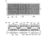
図1(A)(B)に本実施の形態の半導体装置を示す。図1(A)は半導体装置の平面図であり、図1(B)は図1(A)のにおいて線Y−Zの断面図である。 1A and 1B show a semiconductor device of this embodiment mode. 1A is a plan view of the semiconductor device, and FIG. 1B is a cross-sectional view taken along line YZ in FIG.
図1の半導体装置は、半導体集積回路112R、半導体集積回路112G、半導体集積回路112Bをインターポーザ160に実装されて有する構造である。半導体集積回路112R、半導体集積回路112G、半導体集積回路112Bには外部との電気的接続を行うための導電層である端子電極115R1、115R2、115G1、115G2、115B1、115B2が設けられている。
The semiconductor device in FIG. 1 has a structure in which a semiconductor integrated
半導体集積回路112R、半導体集積回路112G、半導体集積回路112Bは、それぞれの端子電極とインターポーザ160に形成された電極161a1、161a2、161b1、161b2、161c1、161c2と異方性導電層162によって電気的に接続されている。インターポーザ160は図1の点線で示すように、表面と裏面とを貫通する開口を有しており、電極161a1と161a2、161b1と161b2、161c1と161c2は開口を介して連続的に接している。従って、電極161a2、161b2、161c2は半導体集積回路112R、半導体集積回路112G、半導体集積回路112Bの電極として、他の基板に実装することができる。
The semiconductor integrated
半導体集積回路112R、半導体集積回路112G、半導体集積回路112Bは、それぞれ透光性基板109R、109G、109B、光電変換素子を含む半導体素子層101R、101G、101B及びカラーフィルタとして機能する有彩色の透光性樹脂層114R、114G、114Bを有しており、カラーセンサとして機能する。本実施の形態においては、半導体集積回路112Rは赤色の透光性樹脂層114R、半導体集積回路112Gは緑色の透光性樹脂層114G、半導体集積回路112Bは青色の透光性樹脂層114Bをそれぞれ有しており、それぞれの透光性樹脂層114R、114G、114Bに着色された色の光を透過し、検知することができる。よって、半導体集積回路112R、半導体集積回路112G、半導体集積回路112Bを含む本実施の形態の半導体装置は、3種類の色(赤色、緑色、青色)の光をそれぞれに検知することのできる半導体装置である。
The semiconductor integrated
さらに、半導体集積回路112R、半導体集積回路112G、半導体集積回路112Bは、透光性基板109R、109G、109Bの半導体素子層101R、101G、101Bの形成面と反対側の一面及び端部(側面)の一部とを少なくとも有彩色の透光性樹脂層114R、114G、114Bで覆う構成である。従って透光性樹脂層114R、114G、114Bが、作製工程、または検査工程において加わる圧力等の外部ストレスからの衝撃吸収層としても機能するため、半導体集積回路112R、112G、112Bのキズ、クラックなどの不良を低減し、信頼性の高い半導体装置を作製することができる。
Further, the semiconductor integrated
有彩色は、黒、灰、白などの無彩色を除く色であり、着色層はカラーフィルタとして機能させるため、その着色された有彩色の光のみを透過する材料で形成される。有彩色としては、赤色、緑色、青色などを用いることができる。また、シアン、マゼンダ、イエロー(黄)などを用いてもよい。 The chromatic color is a color excluding achromatic colors such as black, gray, and white, and the colored layer is formed of a material that transmits only the colored chromatic light in order to function as a color filter. As the chromatic color, red, green, blue, or the like can be used. Further, cyan, magenta, yellow (yellow), or the like may be used.
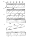
透光性樹脂層114R、114G、114Bは、少なくともカラーフィルタとして機能する有彩色の着色層であり、その上にさらに衝撃吸収層として透明な透光性樹脂層を積層してもよい。図1の半導体装置において、透光性樹脂層を積層する例を図2(A)(B)及び図18(A)(B)に示す。図2(A)図18(A)は半導体装置の平面図であり、図2(B)は図2(A)における線Y−Zの断面図、図18(B)は図18(A)における線Y−Zの断面図である。 The translucent resin layers 114R, 114G, and 114B are at least chromatic colored layers that function as color filters, and a transparent translucent resin layer may be further stacked thereon as an impact absorbing layer. An example in which a light-transmitting resin layer is stacked in the semiconductor device of FIG. 1 is shown in FIGS. 2A and 2B and FIGS. 2A and 18A are plan views of the semiconductor device, FIG. 2B is a cross-sectional view taken along line YZ in FIG. 2A, and FIG. 18B is FIG. 18A. It is sectional drawing of line YZ in.
図2の半導体装置は、透光性樹脂層110R、110G、110Bが各有彩色の透光性樹脂層114R、114G、114B上に積層されている半導体集積回路112R、112G、112Bをインターポーザ160に実装する例である。透光性基板に接して有彩色の透光性樹脂層114R、114G、114Bが形成され、有彩色の透光性樹脂層114R、114G、114Bの上にそれぞれ透明な透光性樹脂層110R、110G、110Bが積層されている。
In the semiconductor device of FIG. 2, the semiconductor integrated
一方、図18の半導体装置は、インターポーザ160に半導体集積回路112R、112G、112Bを実装した後、半導体集積回路112R、112G、112B上を覆うように、有彩色の透光性樹脂層114R、114G、114B上透光性樹脂層110を形成する例である。半導体集積回路112R、112G、112Bをインターポーザ160に実装した後に透光性樹脂層110を形成するため、図18においては、透光性樹脂層110は半導体集積回路112R、112G、112B側面及びインターポーザ160との接続部も連続的に覆う形状とすることができる。
On the other hand, in the semiconductor device of FIG. 18, after the semiconductor integrated
透明な透光性樹脂層110、110R、110G、110Bは、保護層として機能し、衝撃吸収性も向上させ、有彩色の透光性樹脂層114R、114G、114Bの劣化も防止する効果がある。 The transparent translucent resin layers 110, 110R, 110G, and 110B function as a protective layer, improve impact absorption, and have an effect of preventing deterioration of the chromatic translucent resin layers 114R, 114G, and 114B. .
透光性樹脂層の膜厚は1μm〜20μmとすればよい。透光性樹脂層を積層する場合、衝撃吸収層として機能する透光性樹脂層110R、110G、110Bの膜厚と着色層として機能する透光性樹脂層114R、114G、114Bの膜厚は同程度(例えば膜厚1.2μm)でもよいし、異なってもよい。 The film thickness of the translucent resin layer may be 1 μm to 20 μm. When the translucent resin layer is laminated, the film thickness of the translucent resin layers 110R, 110G, and 110B functioning as the shock absorbing layer is the same as the film thickness of the translucent resin layers 114R, 114G, and 114B functioning as the colored layers. The degree (for example, a film thickness of 1.2 μm) may be different or different.
また、衝撃吸収層として機能する透光性樹脂層110R、110G、110Bの膜厚は、着色層として機能する有彩色の透光性樹脂層114R、114G、114Bより厚くてもよい。衝撃吸収層として機能する透光性樹脂層110R、110G、110Bは膜厚を厚く形成することによって、より衝撃吸収層として耐衝撃性を向上させることができる。一方、有彩色の透光性樹脂層114R、114G、114Bは、着色層(カラーフィルタ)として機能させるため、含ませる着色材料の濃度と光の透過率の関係に考慮して、最適な膜厚を適宜制御するとよい。 Moreover, the film thickness of the translucent resin layers 110R, 110G, and 110B that function as the shock absorbing layer may be thicker than the chromatic translucent resin layers 114R, 114G, and 114B that function as the colored layers. By forming the translucent resin layers 110R, 110G, and 110B that function as the shock absorbing layer thick, the shock resistance can be further improved as the shock absorbing layer. On the other hand, the chromatic translucent resin layers 114R, 114G, and 114B function as colored layers (color filters). Therefore, the optimum film thickness is considered in consideration of the relationship between the concentration of the coloring material to be included and the light transmittance. May be controlled appropriately.
例えば、衝撃吸収層として機能する透光性樹脂層110R、110G、110Bの膜厚を、着色層として機能する透光性樹脂層114R、114G、114Bより厚くする場合、例として衝撃吸収層として機能する透光性樹脂層110R、110G、110Bの膜厚を5μm以上10μm以下とし、着色層として機能する透光性樹脂層114R、114G、114Bの膜厚を0.1μm以上1μm以下とすればよい。 For example, when the thickness of the translucent resin layers 110R, 110G, and 110B that function as the shock absorbing layer is made thicker than the translucent resin layers 114R, 114G, and 114B that function as the colored layers, the translucent resin layers function as the shock absorbing layer as an example. The film thickness of the translucent resin layers 110R, 110G, and 110B to be set may be 5 μm to 10 μm, and the film thickness of the translucent resin layers 114R, 114G, and 114B functioning as the colored layers may be 0.1 μm to 1 μm. .
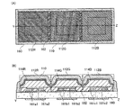
透光性基板109R、109G、109Bの側面に段差を有し、透光性基板109R、109G、109Bの幅寸法は、段差よりも先の部分が小さい。よって、透光性基板109R、109G、109Bの断面は、凸字形状(逆さまのT字ブロック形状)ともいえる。段差よりも先の部分とは、透光性基板109R、109G、109Bにおいて半導体素子層101R、101G、101Bの形成面を下とした場合の上方向の部分である。
The
透光性基板の断面が凸字形状であると、凸字形上において透光性基板端部の切欠き部を埋めるように、透光性樹脂層を設けることができる。 When the cross section of the translucent substrate is a convex shape, the translucent resin layer can be provided so as to fill the notch at the end of the translucent substrate on the convex shape.
本実施の形態の半導体集積回路においては、透光性樹脂層が接している透光性基板の側面は、裾広がりの曲面を有する。透光性基板の側面が裾広がりの曲面を有するために、その曲面に透光性樹脂層を覆うように設けることができる。また、透光性基板の下底面及び上底面は四角形であり、下底面の面積の方が上底面の面積より大きい。透光性基板において下底面の面積の方が上底面の面積より大きいと、下底面と上底面が重なっていない領域の側面に、透光性基板周囲を囲むように透光性樹脂層を設けることができる。 In the semiconductor integrated circuit according to the present embodiment, the side surface of the translucent substrate with which the translucent resin layer is in contact has a curved surface spreading toward the bottom. Since the side surface of the translucent substrate has a curved surface that spreads at the bottom, the translucent resin layer can be provided to cover the curved surface. Further, the lower bottom surface and the upper bottom surface of the translucent substrate are rectangular, and the area of the lower bottom surface is larger than the area of the upper bottom surface. When the area of the lower bottom surface is larger than the area of the upper bottom surface in the light transmitting substrate, a light transmitting resin layer is provided on the side surface of the region where the lower bottom surface and the upper bottom surface do not overlap so as to surround the periphery of the light transmitting substrate. be able to.
大面積な透光性基板を半導体素子層ごとに分断することによって、複数の半導体集積回路をチップ状で取り出す。分断方法において、まず、基板の厚さを薄く加工し、分断にかかる工程時間の短縮、及び分断に用いるダイサーなど加工手段の摩耗を軽減する。さらに分断工程は、一度に行わず、まず、透光性基板に半導体素子層を分断するための溝を形成し、溝の形成された透光性基板上に透光性樹脂層の積層を設ける。その後、透光性樹脂層及び透光性基板を溝において、切断して、複数の半導体集積回路に分断(分割)する。 A plurality of semiconductor integrated circuits are taken out in a chip shape by dividing a large-area translucent substrate into semiconductor element layers. In the cutting method, first, the thickness of the substrate is processed to reduce the process time required for cutting, and wear of processing means such as a dicer used for cutting is reduced. Further, the dividing step is not performed at one time. First, a groove for dividing the semiconductor element layer is formed in the light-transmitting substrate, and a light-transmitting resin layer is stacked on the light-transmitting substrate in which the groove is formed. . Thereafter, the light-transmitting resin layer and the light-transmitting substrate are cut at the groove to be divided (divided) into a plurality of semiconductor integrated circuits.
透光性基板109は断面において、側面が階段状の台形であり、階段状の台形は、上段の厚さが下段の厚さより厚い。溝の形状によっては、図1のように台形の上段は下段に向かって湾曲している形状となる。
The
透光性基板の台形の断面形状において、台形の上段が下段に向かって湾曲している形状であると、湾曲部に設けられる透光性樹脂層の被覆性がよい。 In the trapezoidal cross-sectional shape of the translucent substrate, when the upper stage of the trapezoid is curved toward the lower stage, the coverage of the translucent resin layer provided in the curved part is good.
上記のように本明細書に開示する半導体集積回路は複雑な形状であるため、半導体集積回路の天地左右の判別が容易であり、機械による自動操作においても誤認を低減することができる。 As described above, since the semiconductor integrated circuit disclosed in this specification has a complicated shape, it is easy to distinguish the top and bottom of the semiconductor integrated circuit, and false recognition can be reduced even in automatic operation by a machine.
また、ブラックマトリクスを設ける構成としてもよい。図17にブラックマトリクスとして機能する遮光層を有する半導体装置を示す。図17の半導体装置117R、117G、117Bは、カラーフィルタとして機能する有彩色の透光性樹脂層114R、114G、114B上に選択的に形成された遮光層116R、116G、116Bを有している。遮光層116R、116G、116Bは、スピンコート法などの塗布法によって形成することができ、その他液滴吐出法、印刷法、ディッピング法、ディスペンサ法、刷毛塗り法、スプレー法、フローコート法などによって形成することもできる。印刷法を用いると、遮光層を選択的に形成することができるため、フォトリソグラフィ工程による所望の形状への加工工程を簡略化することができる。
Alternatively, a black matrix may be provided. FIG. 17 shows a semiconductor device having a light shielding layer functioning as a black matrix. The
遮光層116R、116G、116Bは、半導体素子層101R、101G、101Bの光電変換素子が設けられる領域に対応して開口を有するように形成される。遮光層116R、116G、116Bはブラックマトリクスとして機能し、光電変換素子へ外部からの不適切な光が照射し、誤作動を生じないように光を遮断する。よって、遮光層116R、116G、116Bの開口より入射し、カラーフィルタとして機能する有彩色の透光性樹脂層114R、114G、114Bを透過した光のみを光電変換素子は受光することができるため、半導体装置の信頼性が向上する。また、半導体素子層に形成される半導体素子に光が照射されると特性変動が生じる恐れがあるが、遮光層を設けることでそのような不良を防止することができる。 The light shielding layers 116R, 116G, and 116B are formed to have openings corresponding to regions where the photoelectric conversion elements of the semiconductor element layers 101R, 101G, and 101B are provided. The light shielding layers 116R, 116G, and 116B function as a black matrix, and irradiate inappropriate light from the outside to the photoelectric conversion element, and block the light so that malfunction does not occur. Therefore, the photoelectric conversion element can receive only light that has entered through the openings of the light shielding layers 116R, 116G, and 116B and has passed through the chromatic light-transmitting resin layers 114R, 114G, and 114B that function as color filters. The reliability of the semiconductor device is improved. Further, when light is applied to the semiconductor element formed in the semiconductor element layer, there is a risk of characteristic fluctuations. However, such a defect can be prevented by providing a light shielding layer.
以下に、本実施の形態における半導体装置の作製方法を詳細に述べる。 A method for manufacturing a semiconductor device in this embodiment will be described in detail below.
図3(A)に透光性基板100上に設けられた光電変換素子を有する半導体素子層101a、101b、101cを示す。半導体素子層101a、101b、101cはそれぞれ端子電極115a1、115a2、115b1、115b2、115c1、115c2を有している。
FIG. 3A illustrates
次に、透光性基板100の厚さを研削、研磨処理によって薄くする工程を行う。工程時の透光性基板100を固定する固定テープ103に半導体素子層101a、101b、101c側を向けて透光性基板100を固定し、透光性基板100を加工して、厚さの薄い透光性基板102とする(図3(B)参照。)。透光性基板100が厚さ0.5mmのガラス基板であるとすれば、透光性基板102は、0.25〜0.3mm程度に薄型化することが好ましい。透光性基板の厚さを薄く加工することで、透光性基板の分断にかかる工程時間の短縮、及び分断に用いるダイサーなど加工手段の摩耗を軽減することができる。研削処理及び研磨処理は好適に組み合わせて用いることができ、本実施の形態では、研削機により研削した後、研磨機により研磨処理で表面を平坦化する。研磨処理として化学的機械研磨を行ってもよい。
Next, a process of reducing the thickness of the
透光性基板を分断することによって、複数の半導体集積回路をチップ状で取り出す。分断工程は、一度に行わず、まず、透光性基板102に半導体素子層101a、101b、101cを分断するための溝106a、106b、106c、106dをダイサー104のダイシングブレードで形成する(図3(C)参照。)。透光性基板105の溝106a、106b、106c、106dにおいて透光性基板105は意図的に残存させる。残存させる透光性基板105の厚さは、30μm〜100μm(好ましくは30μm〜50μm)程度とすればよい。
By dividing the light-transmitting substrate, a plurality of semiconductor integrated circuits are taken out in a chip shape. First,
次に、溝106a、106b、106c、106dの形成された透光性基板102上に透光性樹脂層113及び透光性樹脂層107の積層を形成する(図3(D)参照。)。透光性樹脂層113、107の材料は、透光性樹脂層形成後の工程において(例えば、インターポーザへの実装時)加熱処理を用いる場合はその加熱温度に耐えうる樹脂材料を用いる。積層して設けられる透光性樹脂層の一方は、カラーフィルタとして機能する有彩色の着色層であり、他方は衝撃吸収層として機能する樹脂層とする。本実施の形態では、透光性樹脂層113を有彩色の着色材料を含んで形成する。
Next, a stack of the light-transmitting
衝撃吸収層として機能する透光性樹脂層107を形成すると、半導体集積回路及び半導体装置に、より耐ストレス性を付与することができる。例えば、本明細書に開示する透光性樹脂層が設けられた半導体集積回路においては、約20Nの圧力を加えても破損することなく耐えることができる。
When the light-transmitting
透光性樹脂層としては、ビニル樹脂、エポキシ樹脂、フェノール樹脂、ノボラック樹脂、アクリル樹脂、メラミン樹脂、ウレタン樹脂、シロキサン樹脂等の樹脂材料を用いることができる。樹脂層の作製方法はスピンコート法などの塗布法を用いることができ、その他液滴吐出法、印刷法、ディッピング法、ディスペンサ法、刷毛塗り法、スプレー法、フローコート法などを用いることもできる。 As the light-transmitting resin layer, a resin material such as a vinyl resin, an epoxy resin, a phenol resin, a novolac resin, an acrylic resin, a melamine resin, a urethane resin, or a siloxane resin can be used. As a method for producing the resin layer, a coating method such as a spin coating method can be used, and a droplet discharge method, a printing method, a dipping method, a dispenser method, a brush coating method, a spray method, a flow coating method, or the like can also be used. .
その後、透光性樹脂層113、107及び透光性基板105を溝106a、106b、106c、106dにおいて、切断して、複数の半導体集積回路に分断(分割)する。本実施の形態では、透光性基板105及び透光性樹脂層113、107を固定テープ111に固定し、透光性基板105側より溝106a、106b、106c、106dに残存する透光性基板102及び透光性樹脂層113、107を、ダイサー108によって切断する。ダイサー108によって、透光性基板105及び透光性樹脂層113、107は分割され、透光性基板109a、109b、109c、透光性樹脂層114a、114b、114c、110a、110b、110cとなる(図3(E)参照。)。本実施の形態では、固定テープ103、111として、ダイシングテープを用いる。
Thereafter, the
溝の形成された透光性基板105及び透光性樹脂層113、107を切断する際は、透光性基板105側でも透光性樹脂層113、107側からでも切断することができる。透光性基板105にアライメント合わせのマーカーを形成する場合は、透光性基板105側よりダイサー等の切断手段を用いて切断すると、切断箇所の正確性を高くすることができる。
When cutting the light-transmitting
以上の工程で、半導体集積回路112a、112b、112cを形成することができる(図3(F)参照。)。透光性樹脂層107及び透光性基板102を切断する切断面の幅を、溝の幅より狭くすることによって、透光性基板側面に、溝に形成された樹脂層を残存させることができる。本実施の形態では、ダイサー104及びダイサー108の幅とは処理領域(ダイサーによって加工される領域)を決定するダイシングブレードの厚さとなる。
Through the above steps, the semiconductor integrated
切断面の幅a1はダイサー104のダイシングブレードの幅a1に、溝の幅は、ダイサー108のダイシングブレードの幅a2によって制御できるため、ダイサー104のダイシングブレードの幅a1よりダイサー108のダイシングブレードの幅a2を狭くすればよい。例えば、本実施の形態では、ダイサー104のダイシングブレードの幅a1を0.16mm、ダイサー108のダイシングブレードの幅a2を0.1mmとする。
Since the width a1 of the cut surface can be controlled by the width a1 of the dicing blade of the
従って、半導体集積回路112a、112b、112cにおいて、半導体素子層101a、101b、101cの設けられていない面及び側面の一部は樹脂層110a、110b、110cで覆われる構造となる。
Therefore, in the semiconductor integrated
透光性基板に形成される溝の形状は加工手段に依存する。本実施の形態ではダイサー104のやや丸みを帯びたダイシングブレードの形状が反映され、溝106a、106b、106c、106dも図1の断面において丸み(曲率を有する)を帯びた形状となっている。ダイシングブレードの形状を矩形とすれば、溝の形状も矩形となり、分断後の半導体集積回路の透光性基板の端部も矩形を有する形状とすることができる。
The shape of the groove formed in the translucent substrate depends on the processing means. In the present embodiment, the shape of the dicing blade having a slightly round shape of the
図9に矩形のダイシングブレードで加工する例を示す。図9(A)は、図1(B)と対応しており、半導体素子層101a、101b、101cが設けられた透光性基板102は固定テープ103上で研削、研磨加工されている。
FIG. 9 shows an example of processing with a rectangular dicing blade. 9A corresponds to FIG. 1B, and the light-transmitting
透光性基板102に半導体素子層101a、101b、101cを分断するための溝126a、126b、126c、126dをダイサー124で形成する(図9(B)参照。)。ダイサー124は矩形のダイシングブレードを用いるために、透光性基板125の溝126a、126b、126c、126dは断面図において矩形となっている。
次に、溝126a、126b、126c、126dの形成された透光性基板125上に透光性樹脂層133、127を形成する(図9(C)参照。)。
Next, light-transmitting
その後、透光性樹脂層133、127及び透光性基板125を溝126a、126b、126c、126dにおいて、切断して、複数の半導体集積回路に分断(分割)する。本実施の形態では、透光性基板125及び透光性樹脂層133、127を固定テープ131に固定し、透光性基板125側より溝126a、126b、126c、126dに残存する透光性基板125及び透光性樹脂層133、127を、ダイサー128によって切断する。ダイサー128によって、透光性基板125及び樹脂層127は分割され、透光性基板129a、129b、129c、透光性樹脂層134a、134b、134c、130a、130b、130cとなる(図9(D)参照。)。
Thereafter, the
以上の工程で、半導体集積回路132a、132b、132cを形成することができる(図9(E)参照。)。半導体集積回路132a、132b、132cは矩形の形状の溝126a、126b、126c、126dの形状を反映し、断面図において側面に段差を有する形状となっている。
Through the above steps, the semiconductor integrated
なお、図9(F)は、図4と同様に図9で形成する半導体集積回路をインターポーザ160に実装する例である。図9(F)において、半導体集積回路132R、132G、132Bは図9(E)と同様に各基板で形成された半導体集積回路である。本実施の形態においては、半導体集積回路132Rは赤色の透光性樹脂層134R、半導体集積回路132Gは緑色の透光性樹脂層134G、半導体集積回路132Bは青色の透光性樹脂層134Bをそれぞれ有しており、それぞれの透光性樹脂層134R、134G、134Bに着色された色の光を透過し、検知することができる。なお、図9(F)において、半導体集積回路132R、132G、132Bはインターポーザ160の電極161a1、161b1、161c1とはんだで実装されており、間に固定のための樹脂層163を設ける例である。
Note that FIG. 9F illustrates an example in which the semiconductor integrated circuit formed in FIG. 9 is mounted on the
また、基板端部での被覆性を向上させるために、基板の厚さは透光性樹脂層と比較して厚いため、透光性樹脂層も厚くすると好ましい。図2のように透光性樹脂層を積層構造とすると厚く形成することができる。透光性樹脂層の構造や膜厚、また切断箇所によっても完成する半導体集積回路の形状を自由に変化させる(異ならせる)ことができる。図2においては、透光性樹脂層を厚く形成しているために、各半導体集積回路において、透光性基板と透光性樹脂層端部とが一致する形状となる。 In addition, since the thickness of the substrate is thicker than that of the translucent resin layer in order to improve the coverage at the edge of the substrate, it is preferable that the translucent resin layer is also thickened. When the translucent resin layer has a laminated structure as shown in FIG. 2, it can be formed thick. The shape of the completed semiconductor integrated circuit can be freely changed (varied) depending on the structure and film thickness of the light-transmitting resin layer and the cut portion. In FIG. 2, since the translucent resin layer is formed thick, in each semiconductor integrated circuit, the translucent substrate and the end of the translucent resin layer coincide with each other.
ダイシングブレードの幅の細いダイサーを用いて分断すると、透光性基板の溝の領域を完成した半導体集積回路に多く残すこともできる。衝撃吸収材として機能する透光性樹脂層を積層すると、半導体集積回路に、より耐ストレス性を付与することができる。 When the dicing blade is cut using a thin dicer, it is possible to leave many groove regions of the light-transmitting substrate in the completed semiconductor integrated circuit. When a light-transmitting resin layer that functions as a shock absorber is stacked, stress resistance can be further imparted to the semiconductor integrated circuit.
また、溝を形成し、溝上に透光性樹脂層を形成するので、溝底面に厚く透光性樹脂層を形成することができる。さらに透光性樹脂層を形成後、透光性樹脂層と透光性基板を積層して切断するため、側面において透光性樹脂層の端部と透光性基板の端部とが一致する。側面において透光性基板の上側の端部が露出しないために、透光性基板の端部の破損や欠けを防止することができる。また、透光性樹脂層を積層により厚く形成すると、半導体集積回路の側面において透光性基板の端部と透光性樹脂層の端部との距離を長くすることができるため、より透光性基板端部に与えるダメージを軽減することができる。 Further, since the groove is formed and the translucent resin layer is formed on the groove, the translucent resin layer can be formed thickly on the bottom surface of the groove. Further, after forming the translucent resin layer, the translucent resin layer and the translucent substrate are laminated and cut, so that the end of the translucent resin layer and the end of the translucent substrate coincide on the side surface. . Since the upper end portion of the translucent substrate is not exposed on the side surface, the end portion of the translucent substrate can be prevented from being damaged or chipped. Further, when the light-transmitting resin layer is formed to be thick by lamination, the distance between the end of the light-transmitting substrate and the end of the light-transmitting resin layer can be increased on the side surface of the semiconductor integrated circuit. Damage to the edge of the conductive substrate can be reduced.
図3のように各基板に形成され、分断された複数の半導体集積回路をインターポーザに実装し、複数の半導体集積回路を有する半導体装置を作製する。 As shown in FIG. 3, a plurality of divided semiconductor integrated circuits formed on each substrate are mounted on an interposer, and a semiconductor device having the plurality of semiconductor integrated circuits is manufactured.
図4(A)において、半導体集積回路112R、112G、112Bは図3と同様に各基板で形成された半導体集積回路である。
In FIG. 4A, semiconductor integrated
半導体集積回路112R、半導体集積回路112G、半導体集積回路112Bは、それぞれ透光性基板109R、109G、109B、光電変換素子を含む半導体素子層101R、101G、101B及びカラーフィルタとして機能する有彩色の透光性樹脂層114R、114G、114Bを有しており、カラーセンサとして機能する。本実施の形態においては、半導体集積回路112Rは赤色の透光性樹脂層114R、半導体集積回路112Gは緑色の透光性樹脂層114G、半導体集積回路112Bは青色の透光性樹脂層114Bをそれぞれ有しており、それぞれの透光性樹脂層114R、114G、114Bに着色された色の光を透過し、検知することができる。
The semiconductor integrated
半導体集積回路112R、半導体集積回路112G、半導体集積回路112Bにおいては、半導体素子層表面に実装時に電気的接続を行う端子電極115R1、115R2、115G1、115G2、115B1、115B2として導電層が設けられている。
In the semiconductor integrated
端子電極115R1、115R2、115G1、115G2、115B1、115B2は湿式法を用いて導電性樹脂によって形成されてもよいし、乾式法を用いて導電性薄膜によって形成されてもよい。また、導電性樹脂層と導電性薄膜とを積層してもよい。 The terminal electrodes 115R1, 115R2, 115G1, 115G2, 115B1, and 115B2 may be formed of a conductive resin using a wet method, or may be formed of a conductive thin film using a dry method. Moreover, you may laminate | stack a conductive resin layer and a conductive thin film.
例えば、スクリーン印刷法を用いて導電層を形成する場合には、粒径が数nmから数十μmの導電体粒子を有機樹脂に溶解または分散させた導電性のペーストを選択的に印刷することによって設けることができる。導電体粒子としては、銀(Ag)、金(Au)、銅(Cu)、ニッケル(Ni)、白金(Pt)、パラジウム(Pd)、タンタル(Ta)、モリブデン(Mo)およびチタン(Ti)等のいずれか一つ以上の金属粒子やハロゲン化銀の微粒子を用いることができる。また、導電性ペーストに含まれる有機樹脂は、金属粒子のバインダー、溶媒、分散剤および被覆材として機能する有機樹脂から選ばれた一つまたは複数を用いることができる。代表的には、エポキシ樹脂、シリコン樹脂等の有機樹脂が挙げられる。また、導電層の形成の際は、導電性のペーストを押し出した後に焼成することが好ましい。また、はんだや鉛フリーのはんだを主成分とする微粒子を用いてもよい。 For example, when a conductive layer is formed using a screen printing method, a conductive paste in which conductive particles having a particle size of several nanometers to several tens of micrometers are dissolved or dispersed in an organic resin is selectively printed. Can be provided. Conductor particles include silver (Ag), gold (Au), copper (Cu), nickel (Ni), platinum (Pt), palladium (Pd), tantalum (Ta), molybdenum (Mo) and titanium (Ti). Any one or more metal particles such as silver halide fine particles can be used. In addition, as the organic resin contained in the conductive paste, one or more selected from organic resins functioning as a binder of metal particles, a solvent, a dispersant, and a coating material can be used. Typically, an organic resin such as an epoxy resin or a silicon resin can be given. In forming the conductive layer, it is preferable to fire after extruding the conductive paste. Further, fine particles mainly composed of solder or lead-free solder may be used.
次に電極161a1、161a2、161b1、161b2、161c1、161c2を含むインターポーザ160に半導体集積回路112R、半導体集積回路112G、半導体集積回路112Bを実装する(図4(B)参照。)。
Next, the semiconductor integrated
また、インターポーザに実装する前に、半導体集積回路に検査工程を行ってもよい。検査工程を行うことで良品を選択してインターポーザに実装し半導体装置を作製することができる。 In addition, an inspection process may be performed on the semiconductor integrated circuit before mounting on the interposer. By performing the inspection process, a non-defective product can be selected and mounted on an interposer to manufacture a semiconductor device.
光電変換素子を含む半導体集積回路は、インターポーザにはんだや異方性導電層によって実装することができる。本実施の形態では、半導体集積回路とインターポーザとの間に異方性導電層162を設けている。
A semiconductor integrated circuit including a photoelectric conversion element can be mounted on an interposer with solder or an anisotropic conductive layer. In this embodiment mode, an anisotropic
また、半導体集積回路と実装されるインターポーザの電極との接続部分の構造としては、基板上の配線と半導体集積回路の端子電極に設けられた導電性の突起物であるバンプとを接触させ、インターポーザと半導体集積回路間を樹脂で固定してもよい。またインターポーザの電極と半導体集積回路の端子電極の間に導電性の粒子を分散させた樹脂を設け、この導電性の粒子で半導体集積回路とインターポーザの電極との接続を行い、導電性の粒子を分散させた有機樹脂で接着、固定してもよい。また、接着に使用する樹脂としては光硬化性の樹脂や熱硬化性のものあるいは自然硬化性の樹脂等を用いることができる。 In addition, as a structure of a connection portion between the semiconductor integrated circuit and the electrode of the interposer to be mounted, the wiring on the substrate and a bump which is a conductive protrusion provided on the terminal electrode of the semiconductor integrated circuit are brought into contact with each other. The semiconductor integrated circuit may be fixed with resin. In addition, a resin in which conductive particles are dispersed is provided between the electrode of the interposer and the terminal electrode of the semiconductor integrated circuit, and the conductive particles are used to connect the semiconductor integrated circuit and the electrode of the interposer. You may adhere and fix with the dispersed organic resin. As the resin used for adhesion, a photo-curing resin, a thermosetting resin, a natural-curing resin, or the like can be used.
また、半導体集積回路とインターポーザとの間に樹脂を設けて固着すると、固着強度が向上するために好ましい。 In addition, it is preferable to provide a resin between the semiconductor integrated circuit and the interposer to fix the resin because the fixing strength is improved.
インターポーザ160は図4において点線で示すように、表面と裏面とを貫通する開口を有しており、電極161a1と161a2、161b1と161b2、161c1と161c2は開口を介して連続的に接している。インターポーザの電極構造の例を図4(C)(D)に示す。
As shown by a dotted line in FIG. 4, the
図4(C)(D)はインターポーザ160に設けられた開口を分断するよう示した断面図である。図4(C)は、インターポーザ160の表裏に形成された161a1と161a2、161b1と161b2、161c1と161c2とを接続するように、導電膜164a1、164a2、164b1、164b2、164c1、164c2が形成されている。導電膜164a1、164a2、164b1、164b2、164c1、164c2はめっき法などにより形成することができる。また、開口は樹脂や導電性材料などによって充填される構造であると好ましい。図4(D)は、インターポーザ160に設けられた開口に導電性材料が充填されている例であり、導電層165a、165b、165cによって、161a1と161a2、161b1と161b2、161c1と161c2とは電気的に接続する。充填する導電性材料として導電性樹脂なども用いることができる。
4C and 4D are cross-sectional views illustrating the openings provided in the
従って、電極161a2、161b2、161c2は半導体集積回路112R、半導体集積回路112G、半導体集積回路112Bの電極として、他の基板に実装することができる。
Therefore, the electrodes 161a2, 161b2, and 161c2 can be mounted on another substrate as electrodes of the semiconductor integrated
インターポーザとしては、有機ポリマー、無機ポリマー、ガラスエポキシ系やセラミック系、ポリイミド、フッ素樹脂などの材料などを用いることができる。 As the interposer, an organic polymer, an inorganic polymer, a glass epoxy type, a ceramic type, a polyimide, a fluororesin, or the like can be used.
また、インターポーザの厚さは50μm〜300μm(代表的には100μm〜200μm)程度である。より厚さの薄いインターポーザを用いると、半導体層装置を薄型化の効果をより高めることができる。図1の半導体装置においては、透光性基板109R、109G、109Bとインターポーザ160はほぼ同じ厚さのものを用いる例を示すが、インターポーザは透光性基板より厚さの厚いものを用いても、薄いものを用いてもよい。
The thickness of the interposer is about 50 μm to 300 μm (typically 100 μm to 200 μm). When an interposer having a thinner thickness is used, the effect of thinning the semiconductor layer device can be further enhanced. In the semiconductor device in FIG. 1, the
また、本実施の形態で示すように、半導体集積回路において、透光性樹脂層が半導体素子層側に露出しないために耐熱性が高く、はんだや異方性導電層を用いて半導体集積回路をインターポーザに実装する際に加熱処理を行うことによる不良の発生を軽減させることができる。 Further, as shown in this embodiment mode, in the semiconductor integrated circuit, since the light-transmitting resin layer is not exposed to the semiconductor element layer side, the heat resistance is high, and the semiconductor integrated circuit is formed using solder or an anisotropic conductive layer. It is possible to reduce the occurrence of defects due to heat treatment when mounted on the interposer.
半導体集積回路において薄く成形された透光性基板は透光性樹脂層で覆われているため工程上取扱い易く、破損などの不良が生じにくい。よって、より薄型の高性能な半導半導体集積回路及び半導体装置を歩留まり良く作製することができる。 A light-transmitting substrate that is thinly formed in a semiconductor integrated circuit is covered with a light-transmitting resin layer, so that it is easy to handle in the process and is less likely to be damaged. Therefore, thinner and higher performance semiconductor semiconductor integrated circuits and semiconductor devices can be manufactured with high yield.
インターポーザに実装される複数の半導体集積回路は、自由に選択することができるため、それぞれ含む有彩色の透光性樹脂の色が異なる半導体集積回路をインターポーザに実装し、カラーセンサとしての機能を有する半導体集積回路を複数色含む半導体装置を作製することができる。 Since a plurality of semiconductor integrated circuits mounted on the interposer can be freely selected, semiconductor integrated circuits having different chromatic color translucent resin colors are mounted on the interposer and have a function as a color sensor. A semiconductor device including a plurality of colors of semiconductor integrated circuits can be manufactured.
また、インターポーザに実装する際に、半導体集積回路に検査工程を行い、良品のみを選別してインターポーザに実装することができるため、作製工程において半導体装置の歩留まりが向上する。特に、半導体集積回路に増幅回路など複雑な構成を含む半導体素子層を有する構成の場合、チップ状の半導体集積回路に不良が生じる恐れがあるため、インターポーザに実装する前に半導体集積回路の不良検査が行えることは有益である。 In addition, when mounting on the interposer, the semiconductor integrated circuit can be inspected and only good products can be selected and mounted on the interposer. Therefore, the yield of the semiconductor device is improved in the manufacturing process. In particular, in the case where the semiconductor integrated circuit has a semiconductor element layer including a complicated configuration such as an amplifier circuit, there is a possibility that the chip-shaped semiconductor integrated circuit may be defective. Therefore, the semiconductor integrated circuit is inspected for defects before being mounted on the interposer. It is beneficial to be able to
さらに、本明細書に開示する半導体集積回路は、透光性基板の半導体素子層の形成面と反対側の一面及び端部(側面)の一部とを少なくとも有彩色の透光性樹脂層で覆う構成である。従って透光性樹脂層が、作製工程、または検査工程において加わる圧力等の外部ストレスからの衝撃吸収層としても機能するため、半導体集積回路のキズ、クラックなどの不良を低減し、信頼性の高い半導体装置を作製することができる。 Further, in the semiconductor integrated circuit disclosed in this specification, at least one chromatic color translucent resin layer is formed on one surface and a part of the end (side surface) opposite to the surface on which the semiconductor element layer of the translucent substrate is formed. It is the structure which covers. Therefore, the translucent resin layer also functions as a shock absorbing layer from external stress such as pressure applied in the manufacturing process or the inspection process, thereby reducing defects such as scratches and cracks in the semiconductor integrated circuit and high reliability. A semiconductor device can be manufactured.
分断される半導体素子層として、基板上に光電変換素子及び電界効果トランジスタを形成する方法を、図5(A)乃至(D)、図6(A)乃至(C)、図7(A)(B)の、断面図を用いて説明する。図7(A)では透光性基板310として、ガラス基板の一つであるAN100を用いる。基板上に形成する電界効果トランジスタとしては、薄膜トランジスタを用いることにより、基板上に、光電変換素子と薄膜トランジスタを同一工程で作製することができるため、半導体集積回路の量産化がし易いといった利点がある。なお、カラーフィルタとして機能する透光性樹脂層及び透光性基板を通過して光電変換素子に光を照射する。
As a semiconductor element layer to be divided, a method for forming a photoelectric conversion element and a field effect transistor over a substrate is described with reference to FIGS. 5A to 5D, FIGS. 6A to 6C, and FIG. This will be described with reference to the sectional view of B). In FIG. 7A, as the light-transmitting
まず、プラズマCVD法で下地絶縁膜312となる窒素を含む酸化珪素膜(膜厚100nm)を形成し、さらに大気にふれることなく、半導体膜例えば水素を含む非晶質珪素膜(膜厚54nm)を積層形成する。また、下地絶縁膜312は酸化珪素膜、窒化珪素膜、窒素を含む酸化珪素膜を用いた積層してもよい。例えば、下地絶縁膜312として、酸素を含む窒化珪素膜を50nm、さらに窒素を含む酸化珪素膜を100nm積層した膜を形成してもよい。なお、窒素を含む酸化珪素膜や窒化珪素膜は、ガラス基板からのアルカリ金属などの不純物拡散を防止するブロッキング層として機能する。
First, a silicon oxide film (thickness: 100 nm) containing nitrogen is formed as a
半導体素子が有する半導体層を形成する材料は、シランやゲルマンに代表される半導体材料ガスを用いて気相成長法やスパッタリング法で作製される非晶質(アモルファス、以下「AS」ともいう。)半導体、該非晶質半導体を光エネルギーや熱エネルギーを利用して結晶化させた多結晶半導体、或いは微結晶(セミアモルファス若しくはマイクロクリスタルとも呼ばれる。以下「SAS」ともいう。)半導体などを用いることができる。半導体層はスパッタ法、LPCVD法、またはプラズマCVD法等により成膜することができる。 A material for forming a semiconductor layer included in a semiconductor element is amorphous (hereinafter also referred to as “AS”) manufactured by a vapor deposition method or a sputtering method using a semiconductor material gas typified by silane or germane. A semiconductor, a polycrystalline semiconductor obtained by crystallizing the amorphous semiconductor using light energy or thermal energy, a microcrystalline (also referred to as semi-amorphous or microcrystal, hereinafter referred to as “SAS”) semiconductor, or the like is used. it can. The semiconductor layer can be formed by sputtering, LPCVD, plasma CVD, or the like.
微結晶半導体膜は、ギブスの自由エネルギーを考慮すれば非晶質と単結晶の中間的な準安定状態に属するものである。すなわち、自由エネルギー的に安定な第3の状態を有する半導体であって、短距離秩序を持ち格子歪みを有する。柱状または針状結晶が基板表面に対して法線方向に成長している。微結晶半導体の代表例である微結晶シリコンは、そのラマンスペクトルが単結晶シリコンを示す520cm−1よりも低波数側に、シフトしている。即ち、単結晶シリコンを示す520cm−1とアモルファスシリコンを示す480cm−1の間に微結晶シリコンのラマンスペクトルのピークがある。また、未結合手(ダングリングボンド)を終端するため水素またはハロゲンを少なくとも1原子%またはそれ以上含ませている。さらに、ヘリウム、アルゴン、クリプトン、ネオンなどの希ガス元素を含ませて格子歪みをさらに助長させることで、安定性が増し良好な微結晶半導体膜が得られる。 A microcrystalline semiconductor film belongs to a metastable state between amorphous and single crystal in consideration of Gibbs free energy. That is, it is a semiconductor having a third state that is stable in terms of free energy, and has a short-range order and lattice distortion. Columnar or needle-like crystals grow in the normal direction with respect to the substrate surface. Microcrystalline silicon which is a typical example of a microcrystalline semiconductor has a Raman spectrum shifted to a lower wave number side than 520 cm −1 indicating single crystal silicon. That is, the peak of the Raman spectrum of microcrystalline silicon is between 520 cm −1 indicating single crystal silicon and 480 cm −1 indicating amorphous silicon. In addition, at least 1 atomic% or more of hydrogen or halogen is contained to terminate dangling bonds (dangling bonds). Further, by adding a rare gas element such as helium, argon, krypton, or neon to further promote lattice distortion, stability can be improved and a good microcrystalline semiconductor film can be obtained.
この微結晶半導体膜は、周波数が数十MHz〜数百MHzの高周波プラズマCVD法、または周波数が1GHz以上のマイクロ波プラズマCVD装置により形成することができる。代表的には、SiH4、Si2H6、SiH2Cl2、SiHCl3、SiCl4、SiF4などの水素化珪素を水素で希釈して形成することができる。また、水素化珪素及び水素に加え、ヘリウム、アルゴン、クリプトン、ネオンから選ばれた一種または複数種の希ガス元素で希釈して微結晶半導体膜を形成することができる。これらのときの水素化珪素に対して水素の流量比を5倍以上200倍以下、好ましくは50倍以上150倍以下、更に好ましくは100倍とする。 This microcrystalline semiconductor film can be formed by a high-frequency plasma CVD method with a frequency of several tens to several hundreds of MHz or a microwave plasma CVD apparatus with a frequency of 1 GHz or more. Typically, silicon hydride such as SiH 4 , Si 2 H 6 , SiH 2 Cl 2 , SiHCl 3 , SiCl 4 , and SiF 4 can be formed by diluting with hydrogen. In addition to silicon hydride and hydrogen, the microcrystalline semiconductor film can be formed by dilution with one or more kinds of rare gas elements selected from helium, argon, krypton, and neon. The flow rate ratio of hydrogen to silicon hydride at these times is 5 to 200 times, preferably 50 to 150 times, and more preferably 100 times.
アモルファス半導体としては、代表的には水素化アモルファスシリコン、結晶性半導体としては代表的にはポリシリコンなどがあげられる。ポリシリコン(多結晶シリコン)には、800℃以上のプロセス温度を経て形成されるポリシリコンを主材料として用いた所謂高温ポリシリコンや、600℃以下のプロセス温度で形成されるポリシリコンを主材料として用いた所謂低温ポリシリコン、また結晶化を促進する元素などを用いて、非晶質シリコンを結晶化させたポリシリコンなどを含んでいる。もちろん、前述したように、微結晶半導体又は半導体層の一部に結晶相を含む半導体を用いることもできる。 A typical example of an amorphous semiconductor is hydrogenated amorphous silicon, and a typical example of a crystalline semiconductor is polysilicon. Polysilicon (polycrystalline silicon) is mainly made of so-called high-temperature polysilicon using polysilicon formed through a process temperature of 800 ° C. or higher as a main material, or polysilicon formed at a process temperature of 600 ° C. or lower. And so-called low-temperature polysilicon, and polysilicon obtained by crystallizing amorphous silicon using an element that promotes crystallization. Needless to say, as described above, a microcrystalline semiconductor or a semiconductor including a crystalline phase in part of a semiconductor layer can be used.
また、半導体の材料としてはシリコン(Si)、ゲルマニウム(Ge)などの単体のほかGaAs、InP、SiC、ZnSe、GaN、SiGeなどのような化合物半導体も用いることができる。また酸化物半導体である酸化亜鉛(ZnO)、酸化スズ(SnO2)なども用いることができ、ZnOを半導体層に用いる場合、ゲート絶縁層をY2O3、Al2O3、TiO2、それらの積層などを用いるとよく、ゲート電極層、ソース電極層、ドレイン電極層としては、ITO、Au、Tiなどを用いるとよい。また、ZnOにInやGaなどを添加することもできる。 As a semiconductor material, a compound semiconductor such as GaAs, InP, SiC, ZnSe, GaN, or SiGe can be used in addition to a simple substance such as silicon (Si) or germanium (Ge). Alternatively, zinc oxide (ZnO), tin oxide (SnO 2 ), or the like which is an oxide semiconductor can be used. When ZnO is used for the semiconductor layer, the gate insulating layer is formed of Y 2 O 3 , Al 2 O 3 , TiO 2 , A stacked layer of them is preferably used, and ITO, Au, Ti, or the like is preferably used for the gate electrode layer, the source electrode layer, and the drain electrode layer. In addition, In, Ga, or the like can be added to ZnO.
半導体層に、結晶性半導体膜を用いる場合、その結晶性半導体膜の作製方法は、種々の方法(レーザ結晶化法、熱結晶化法、またはニッケルなどの結晶化を助長する元素を用いた熱結晶化法等)を用いれば良い。また、SASである微結晶半導体をレーザ照射して結晶化し、結晶性を高めることもできる。結晶化を助長する元素を導入しない場合は、非晶質珪素膜にレーザ光を照射する前に、窒素雰囲気下500℃で1時間加熱することによって非晶質珪素膜の含有水素濃度を1×10²⁰atoms/cm3以下にまで放出させる。これは水素を多く含んだ非晶質珪素膜にレーザ光を照射すると非晶質珪素膜が破壊されてしまうからである。 In the case where a crystalline semiconductor film is used for a semiconductor layer, a crystalline semiconductor film can be formed by various methods (laser crystallization method, thermal crystallization method, or heat using an element that promotes crystallization such as nickel). A crystallization method or the like may be used. In addition, a microcrystalline semiconductor that is a SAS can be crystallized by laser irradiation to improve crystallinity. In the case where an element for promoting crystallization is not introduced, the amorphous silicon film is heated at 500 ° C. for 1 hour in a nitrogen atmosphere before irradiating the amorphous silicon film with laser light, whereby the concentration of hydrogen contained in the amorphous silicon film is set to 1 ×. Release to 10 20 atoms / cm 3 or less. This is because the amorphous silicon film is destroyed when the amorphous silicon film containing a large amount of hydrogen is irradiated with laser light.
非晶質半導体層への金属元素の導入の仕方としては、当該金属元素を非晶質半導体膜の表面又はその内部に存在させ得る手法であれば特に限定はなく、例えばスパッタ法、CVD法、プラズマ処理法(プラズマCVD法も含む)、吸着法、金属塩の溶液を塗布する方法を使用することができる。このうち溶液を用いる方法は簡便であり、金属元素の濃度調整が容易であるという点で有用である。また、このとき非晶質半導体膜の表面の濡れ性を改善し、非晶質半導体膜の表面全体に水溶液を行き渡らせるため、酸素雰囲気中でのUV光の照射、熱酸化法、ヒドロキシラジカルを含むオゾン水又は過酸化水素による処理等により、酸化膜を成膜することが望ましい。 The method for introducing the metal element into the amorphous semiconductor layer is not particularly limited as long as the metal element can be present on the surface of the amorphous semiconductor film or inside the amorphous semiconductor film. For example, sputtering, CVD, A plasma treatment method (including a plasma CVD method), an adsorption method, or a method of applying a metal salt solution can be used. Among these, the method using a solution is simple and useful in that the concentration of the metal element can be easily adjusted. At this time, in order to improve the wettability of the surface of the amorphous semiconductor film and to spread the aqueous solution over the entire surface of the amorphous semiconductor film, irradiation with UV light in an oxygen atmosphere, thermal oxidation method, hydroxy radical It is desirable to form an oxide film by treatment with ozone water or hydrogen peroxide.
また、非晶質半導体膜を結晶化し、結晶性半導体膜を形成する結晶化工程で、非晶質半導体膜に結晶化を促進する元素(触媒元素、金属元素とも示す)を添加し、熱処理(550℃〜750℃で3分〜24時間)により結晶化を行ってもよい。結晶化を助長(促進)する元素としては、鉄(Fe)、ニッケル(Ni)、コバルト(Co)、ルテニウム(Ru)、ロジウム(Rh)、パラジウム(Pd)、オスミウム(Os)、イリジウム(Ir)、白金(Pt)、銅(Cu)及び金(Au)から選ばれた一種又は複数種類を用いることができる。 In the crystallization step of crystallizing the amorphous semiconductor film to form the crystalline semiconductor film, an element (also referred to as a catalyst element or a metal element) that promotes crystallization is added to the amorphous semiconductor film, and heat treatment ( Crystallization may be carried out at 550 ° C. to 750 ° C. for 3 minutes to 24 hours. As elements that promote (promote) crystallization, iron (Fe), nickel (Ni), cobalt (Co), ruthenium (Ru), rhodium (Rh), palladium (Pd), osmium (Os), iridium (Ir) ), Platinum (Pt), copper (Cu), and gold (Au) can be used.
結晶化を助長する元素を結晶性半導体膜から除去、又は軽減するため、結晶性半導体膜に接して、不純物元素を含む半導体膜を形成し、ゲッタリングシンクとして機能させる。不純物元素としては、n型を付与する不純物元素、p型を付与する不純物元素や希ガス元素などを用いることができ、例えばリン(P)、窒素(N)、ヒ素(As)、アンチモン(Sb)、ビスマス(Bi)、ボロン(B)、ヘリウム(He)、ネオン(Ne)、アルゴン(Ar)、Kr(クリプトン)、Xe(キセノン)から選ばれた一種または複数種を用いることができる。結晶化を促進する元素を含む結晶性半導体膜に、希ガス元素を含む半導体膜を形成し、熱処理(550℃〜750℃で3分〜24時間)を行う。結晶性半導体膜中に含まれる結晶化を促進する元素は、希ガス元素を含む半導体膜中に移動し、結晶性半導体膜中の結晶化を促進する元素は除去、又は軽減される。その後、ゲッタリングシンクとなった希ガス元素を含む半導体膜を除去する。 In order to remove or reduce an element that promotes crystallization from the crystalline semiconductor film, a semiconductor film containing an impurity element is formed in contact with the crystalline semiconductor film and functions as a gettering sink. As the impurity element, an impurity element imparting n-type conductivity, an impurity element imparting p-type conductivity, a rare gas element, or the like can be used. For example, phosphorus (P), nitrogen (N), arsenic (As), antimony (Sb ), Bismuth (Bi), boron (B), helium (He), neon (Ne), argon (Ar), Kr (krypton), and Xe (xenon) can be used. A semiconductor film containing a rare gas element is formed over the crystalline semiconductor film containing the element that promotes crystallization, and heat treatment (at 550 ° C. to 750 ° C. for 3 minutes to 24 hours) is performed. The element that promotes crystallization contained in the crystalline semiconductor film moves into the semiconductor film containing a rare gas element, and the element that promotes crystallization in the crystalline semiconductor film is removed or reduced. After that, the semiconductor film containing a rare gas element that has become a gettering sink is removed.
非晶質半導体膜の結晶化は、熱処理とレーザ光照射による結晶化を組み合わせてもよく、熱処理やレーザ光照射を単独で、複数回行っても良い。 Crystallization of the amorphous semiconductor film may be a combination of heat treatment and crystallization by laser light irradiation, or may be performed multiple times by heat treatment or laser light irradiation alone.
また、結晶性半導体膜を、直接基板にプラズマ法により形成しても良い。また、プラズマ法を用いて、結晶性半導体膜を選択的に基板に形成してもよい。 Alternatively, the crystalline semiconductor film may be directly formed over the substrate by a plasma method. Alternatively, a crystalline semiconductor film may be selectively formed over the substrate by a plasma method.
本実施の形態では、半導体膜として触媒元素を用いた結晶化方法を用いて多結晶珪素膜を形成する。重量換算で10ppmのニッケルを含む酢酸ニッケル溶液をスピナーで添加する。なお、溶液を添加する方法に代えてスパッタ法でニッケル元素を全面に散布する方法を用いてもよい。次いで、加熱処理を行い結晶化させて結晶構造を有する半導体膜(ここでは多結晶珪素膜)を形成する。ここでは熱処理(500℃、1時間)の後、結晶化のための熱処理(550℃、4時間)を行って多結晶珪素膜を得る。 In this embodiment mode, a polycrystalline silicon film is formed using a crystallization method using a catalytic element as a semiconductor film. A nickel acetate solution containing 10 ppm nickel by weight is added with a spinner. Instead of adding the solution, a method of spraying nickel element over the entire surface by sputtering may be used. Next, heat treatment is performed for crystallization to form a semiconductor film having a crystal structure (here, a polycrystalline silicon film). Here, after heat treatment (500 ° C., 1 hour), heat treatment for crystallization (550 ° C., 4 hours) is performed to obtain a polycrystalline silicon film.
次いで、多結晶珪素膜表面の酸化膜を希フッ酸等で除去する。その後、結晶化率を高め、結晶粒内に残される欠陥を補修するためのレーザ光(XeCl:波長308nm)の照射を大気中、または酸素雰囲気中で行う。 Next, the oxide film on the surface of the polycrystalline silicon film is removed with dilute hydrofluoric acid or the like. After that, irradiation with laser light (XeCl: wavelength 308 nm) for increasing the crystallization rate and repairing defects left in the crystal grains is performed in the air or an oxygen atmosphere.
レーザ光には波長400nm以下のエキシマレーザ光や、YAGレーザの第2高調波又は第3高調波を用いる。ここでは、繰り返し周波数10〜1000Hz程度のパルスレーザ光を用い、当該レーザ光を光学系にて100〜500mJ/cm2に集光し、90〜95%のオーバーラップ率をもって照射し、シリコン膜表面を走査させればよい。本実施の形態では、繰り返し周波数30Hz、エネルギー密度470mJ/cm2でレーザ光の照射を大気中で行なう。 As the laser light, excimer laser light having a wavelength of 400 nm or less or the second harmonic or the third harmonic of a YAG laser is used. Here, a pulsed laser beam having a repetition frequency of about 10 to 1000 Hz is used, the laser beam is condensed to 100 to 500 mJ / cm 2 by an optical system, and irradiated with an overlap rate of 90 to 95%. May be scanned. In this embodiment mode, laser light irradiation is performed in the atmosphere at a repetition frequency of 30 Hz and an energy density of 470 mJ / cm 2 .
なお、大気中、または酸素雰囲気中で行うため、レーザ光の照射により表面に酸化膜が形成される。なお、本実施の形態ではパルスレーザを用いた例を示したが、連続発振のレーザを用いてもよく、半導体膜の結晶化に際し、大粒径に結晶を得るためには、連続発振が可能な固体レーザを用い、基本波の第2高調波〜第4高調波を適用するのが好ましい。代表的には、Nd:YVO4レーザ(基本波1064nm)の第2高調波(532nm)や第3高調波(355nm)を適用すればよい。 Note that an oxide film is formed on the surface by irradiation with a laser beam because it is performed in the air or in an oxygen atmosphere. Note that although an example using a pulse laser is shown in this embodiment mode, a continuous wave laser may be used, and continuous oscillation is possible in order to obtain a crystal with a large grain size when a semiconductor film is crystallized. It is preferable to use a solid-state laser and apply the second to fourth harmonics of the fundamental wave. Typically, a second harmonic (532 nm) or a third harmonic (355 nm) of an Nd: YVO 4 laser (fundamental wave 1064 nm) may be applied.
連続発振のレーザを用いる場合には、出力10Wの連続発振のYVO4レーザから射出されたレーザ光を非線形光学素子により高調波に変換する。また、共振器の中にYVO4結晶と非線形光学素子を入れて、高調波を射出する方法もある。そして、好ましくは光学系により照射面にて矩形状または楕円形状のレーザ光に成形して、被処理体に照射する。このときのエネルギー密度は0.01〜100MW/cm2程度(好ましくは0.1〜10MW/cm2)が必要である。そして、10〜2000cm/s程度の速度でレーザ光に対して相対的に半導体膜を移動させて照射すればよい。 In the case of using a continuous wave laser, laser light emitted from a continuous wave YVO 4 laser having an output of 10 W is converted into a harmonic by a nonlinear optical element. There is also a method of emitting harmonics by putting a YVO 4 crystal and a nonlinear optical element in a resonator. Then, it is preferably formed into a rectangular or elliptical laser beam on the irradiation surface by an optical system, and irradiated to the object to be processed. At this time, the energy density of approximately 0.01 to 100 MW / cm 2 (preferably 0.1 to 10 MW / cm 2) is required. Then, irradiation may be performed by moving the semiconductor film relative to the laser light at a speed of about 10 to 2000 cm / s.
次いで、上記レーザ光の照射により形成された酸化膜に加え、オゾン水で表面を120秒処理して合計1〜5nmの酸化膜からなるバリア層を形成する。このバリア層は、結晶化させるために添加した触媒元素、例えばニッケル(Ni)を膜中から除去するために形成する。ここではオゾン水を用いてバリア層を形成したが、酸素雰囲気下の紫外線の照射で結晶構造を有する半導体膜の表面を酸化する方法や酸素プラズマ処理により結晶構造を有する半導体膜の表面を酸化する方法やプラズマCVD法やスパッタ法や蒸着法などで1〜10nm程度の酸化膜を堆積してバリア層を形成してもよい。また、バリア層を形成する前にレーザ光の照射により形成された酸化膜を除去してもよい。 Next, in addition to the oxide film formed by the laser light irradiation, the surface is treated with ozone water for 120 seconds to form a barrier layer made of an oxide film having a total thickness of 1 to 5 nm. This barrier layer is formed to remove a catalyst element added for crystallization, for example, nickel (Ni) from the film. Here, the barrier layer is formed using ozone water, but the surface of the semiconductor film having a crystal structure is oxidized by a method of oxidizing the surface of the semiconductor film having a crystal structure by irradiation with ultraviolet light in an oxygen atmosphere or the oxygen plasma treatment. The barrier layer may be formed by depositing an oxide film of about 1 to 10 nm by a method, plasma CVD method, sputtering method or vapor deposition method. Further, the oxide film formed by laser light irradiation may be removed before forming the barrier layer.
次いで、バリア層上にスパッタ法にてゲッタリングサイトとなるアルゴン元素を含む非晶質珪素膜を10nm〜400nm、ここでは膜厚100nmで成膜する。ここでは、アルゴン元素を含む非晶質珪素膜は、シリコンターゲットを用いてアルゴンを含む雰囲気下で形成する。プラズマCVD法を用いてアルゴン元素を含む非晶質珪素膜を形成する場合、成膜条件は、モノシランとアルゴンの流量比(SiH4:Ar)を1:99とし、成膜圧力を6.665Paとし、RFパワー密度を0.087W/cm2とし、成膜温度を350℃とする。 Next, an amorphous silicon film containing an argon element serving as a gettering site is formed with a thickness of 10 to 400 nm, here 100 nm, over the barrier layer by a sputtering method. Here, the amorphous silicon film containing an argon element is formed using a silicon target in an atmosphere containing argon. In the case where an amorphous silicon film containing an argon element is formed using a plasma CVD method, the film formation conditions are as follows: the flow ratio of monosilane to argon (SiH 4 : Ar) is 1:99, and the film formation pressure is 6.665 Pa. The RF power density is 0.087 W / cm 2 and the film formation temperature is 350 ° C.
その後、650℃に加熱された炉に入れて3分の熱処理を行い触媒元素を除去(ゲッタリング)する。これにより結晶構造を有する半導体膜中の触媒元素濃度が低減される。炉に代えてランプアニール装置を用いてもよい。 Thereafter, the catalyst element is removed (gettering) by performing a heat treatment for 3 minutes in a furnace heated to 650 ° C. As a result, the concentration of the catalytic element in the semiconductor film having a crystal structure is reduced. A lamp annealing apparatus may be used instead of the furnace.
次いで、バリア層をエッチングストッパとして、ゲッタリングサイトであるアルゴン元素を含む非晶質珪素膜を選択的に除去した後、バリア層を希フッ酸で選択的に除去する。なお、ゲッタリングの際、ニッケルは酸素濃度の高い領域に移動しやすい傾向があるため、酸化膜からなるバリア層をゲッタリング後に除去することが望ましい。 Next, the amorphous silicon film containing an argon element which is a gettering site is selectively removed using the barrier layer as an etching stopper, and then the barrier layer is selectively removed with dilute hydrofluoric acid. Note that during gettering, nickel tends to move to a region with a high oxygen concentration, and thus it is desirable to remove the barrier layer made of an oxide film after gettering.
なお、触媒元素を用いて半導体膜の結晶化を行わない場合には、上述したバリア層の形成、ゲッタリングサイトの形成、ゲッタリングのための熱処理、ゲッタリングサイトの除去、バリア層の除去などの工程は不要である。 Note that in the case where the semiconductor film is not crystallized using a catalytic element, the above-described barrier layer formation, gettering site formation, heat treatment for gettering, gettering site removal, barrier layer removal, etc. This step is unnecessary.
次いで、得られた結晶構造を有する半導体膜(例えば結晶性珪素膜)の表面にオゾン水で薄い酸化膜を形成した後、第1のフォトマスクを用いてレジストからなるマスクを形成し、所望の形状にエッチング処理して島状に分離された半導体層331を形成する(図5(A)参照。)。半導体層331を形成した後、レジストからなるマスクを除去する。
Next, after forming a thin oxide film with ozone water on the surface of the obtained semiconductor film having a crystalline structure (for example, a crystalline silicon film), a mask made of resist is formed using a first photomask, and a desired film is formed. A
次いで、必要があればトランジスタのしきい値電圧を制御するために微量な不純物元素(ホウ素またはリン)のドーピングを行う。ここでは、ジボラン(B2H6)を質量分離しないでプラズマ励起したイオンドープ法を用いる。 Next, if necessary, a small amount of impurity element (boron or phosphorus) is doped in order to control the threshold voltage of the transistor. Here, an ion doping method in which diborane (B 2 H 6 ) is plasma-excited without mass separation is used.
次いで、フッ酸を含むエッチャントで酸化膜を除去すると同時に半導体層331の表面を洗浄した後、ゲート絶縁膜313となる絶縁膜を形成する。
Next, the oxide film is removed with an etchant containing hydrofluoric acid, and at the same time, the surface of the
ゲート絶縁膜313は酸化珪素、若しくは酸化珪素と窒化珪素の積層構造で形成すればよい。ゲート絶縁膜313は、プラズマCVD法や減圧CVD法により絶縁膜を堆積することで形成しても良いし、プラズマ処理による固相酸化若しくは固相窒化で形成すると良い。半導体層を、プラズマ処理により酸化又は窒化することにより形成するゲート絶縁膜は、緻密で絶縁耐圧が高く信頼性に優れているためである。例えば、亜酸化窒素(N2O)をArで1〜3倍(流量比)に希釈して、10〜30Paの圧力にて3〜5kWのマイクロ波(2.45GHz)電力を印加して半導体層の表面を酸化若しくは窒化させる。この処理により1nm〜10nm(好ましくは2nm〜6nm)の絶縁膜を形成する。さらに亜酸化窒素(N2O)とシラン(SiH4)を導入し、10〜30Paの圧力にて3〜5kWのマイクロ波(2.45GHz)電力を印加して気相成長法により酸化窒化シリコン膜を形成してゲート絶縁膜を形成する。固相反応と気相成長法による反応を組み合わせることにより界面準位密度が低く絶縁耐圧の優れたゲート絶縁膜を形成することができる。
The
また、ゲート絶縁膜313として、二酸化ジルコニウム、酸化ハフニウム、二酸化チタン、五酸化タンタルなどの高誘電率材料を用いても良い。ゲート絶縁膜313に高誘電率材料を用いることにより、ゲートリーク電流を低減することができる。
As the
本実施の形態では、ゲート絶縁膜313としてプラズマCVD法により115nmの厚さで窒素を含む酸化珪素膜を形成する。
In this embodiment, a silicon oxide film containing nitrogen with a thickness of 115 nm is formed as the
次いで、ゲート絶縁膜313上に金属膜を形成した後、第2のフォトマスクを用いて、ゲート電極334、配線314及び315、端子電極350を形成する(図5(B)参照)。この金属膜として、例えば窒化タンタル及びタングステン(W)をそれぞれ30nm、370nm積層した膜を用いる。
Next, after a metal film is formed over the
また、ゲート電極334、配線314及び315、端子電極350として、上記以外にもチタン(Ti)、タングステン(W)、タンタル(Ta)、モリブデン(Mo)、ネオジム(Nd)、コバルト(Co)、ジルコニウム(Zr)、亜鉛(Zn)、ルテニウム(Ru)、ロジウム(Rh)、パラジウム(Pd)、オスミウム(Os)、イリジウム(Ir)、白金(Pt)、アルミニウム(Al)、金(Au)、銀(Ag)、銅(Cu)から選ばれた元素、または前記元素を主成分とする合金材料若しくは化合物材料からなる単層膜、或いは、これらの窒化物、例えば、窒化チタン、窒化タングステン、窒化タンタル、窒化モリブデンからなる単層膜を用いることができる。
In addition to the above, as the
また、ゲート電極334、配線314及び315、端子電極350に可視光に対して透光性を有する透光性の材料を用いることもできる。透光性の導電材料としては、インジウム錫酸化物(ITO)、酸化珪素を含むインジウム錫酸化物(ITSO)、有機インジウム、有機スズ、酸化亜鉛等を用いることができる。また、酸化亜鉛(ZnO)を含むインジウム亜鉛酸化物(IZO(Indium Zinc Oxide))、酸化亜鉛(ZnO)、ZnOにガリウム(Ga)をドープしたもの、酸化スズ(SnO2)、酸化タングステンを含むインジウム酸化物、酸化タングステンを含むインジウム亜鉛酸化物、酸化チタンを含むインジウム酸化物、酸化チタンを含むインジウム錫酸化物などを用いてもよい。
Alternatively, a light-transmitting material having a property of transmitting visible light can be used for the
次いで、半導体層331への一導電型を付与する不純物の導入を行って、トランジスタ373のソース領域またはドレイン領域337の形成を行う(図5(C)参照)。本実施の形態ではnチャネル型トランジスタを形成するので、n型を付与する不純物、例えばリン(P)、砒素(As)など半導体層331に導入する。pチャネル型トランジスタを形成する場合は、p型を付与する不純物、例えばボロン(B)を半導体層331に導入すればよい。
Next, an impurity imparting one conductivity type is introduced into the
次いで、CVD法により酸化珪素膜を含む第1の層間絶縁膜(図示しない)を50nm形成した後、それぞれの島状半導体領域に添加された不純物元素を活性化処理する工程を行う。この活性化工程は、ランプ光源を用いたラピッドサーマルアニール法(RTA法)、或いはYAGレーザまたはエキシマレーザを裏面から照射する方法、或いは炉を用いた熱処理、或いはこれらの方法のうち、いずれかと組み合わせた方法によって行う。 Next, after forming a first interlayer insulating film (not shown) including a silicon oxide film by CVD with a thickness of 50 nm, a step of activating the impurity element added to each island-like semiconductor region is performed. This activation process is performed by a rapid thermal annealing method (RTA method) using a lamp light source, a method of irradiating a YAG laser or an excimer laser from the back surface, a heat treatment using a furnace, or a combination thereof. By different methods.
次いで、水素及び酸素を含む窒化珪素膜を含む第2の層間絶縁膜316を、例えば10nmの膜厚で形成する。
Next, a second
次いで、第2の層間絶縁膜316上に絶縁性材料から成る第3の層間絶縁膜317を形成する(図5(D)参照)。第3の層間絶縁膜317はCVD法で得られる絶縁膜を用いることができる。本実施の形態においては密着性を向上させるため、第3の層間絶縁膜317として、900nmの膜厚で形成した窒素を含む酸化珪素膜を形成する。
Next, a third
次に、熱処理(300〜550℃で1〜12時間の熱処理、例えば窒素雰囲気中410℃で1時間)を行い、半導体層を水素化する。この工程は第2の層間絶縁膜316に含まれる水素により半導体層のダングリングボンドを終端させるために行うものである。ゲート絶縁膜313の存在に関係なく半導体層を水素化することができる。
Next, heat treatment (300 to 550 ° C. for 1 to 12 hours, for example, in a nitrogen atmosphere at 410 ° C. for 1 hour) is performed to hydrogenate the semiconductor layer. This step is performed in order to terminate dangling bonds in the semiconductor layer with hydrogen contained in the second
また第3の層間絶縁膜317として、シロキサンを用いた絶縁膜、及びそれらの積層構造を用いることも可能である。シロキサンは、シリコン(Si)と酸素(O)との結合で骨格構造で構成される。置換基として、少なくとも水素を含む化合物(例えばアルキル基、アリール基)が用いられる。置換基として、フッ素を用いてもよい。または置換基として、少なくとも水素を含む化合物と、フッ素とを用いてもよい。
Further, as the third
第3の層間絶縁膜317としてシロキサンを用いた絶縁膜、及びそれらの積層構造を用いた場合は、第2の層間絶縁膜316を形成後、半導体層を水素化するための熱処理を行い、次に第3の層間絶縁膜317を形成することもできる。
In the case where an insulating film using siloxane and a stacked structure thereof are used as the third
次いで、第3のフォトマスクを用いてレジストからなるマスクを形成し、第1の層間絶縁膜、第2の層間絶縁膜316及び第3の層間絶縁膜317またはゲート絶縁膜313を選択的にエッチングしてコンタクトホールを形成する。そして、レジストからなるマスクを除去する。
Next, a resist mask is formed using a third photomask, and the first interlayer insulating film, the second
なお、第3の層間絶縁膜317は必要に応じて形成すればよく、第3の層間絶縁膜317を形成しない場合は、第2の層間絶縁膜316を形成後に第1の層間絶縁膜、第2の層間絶縁膜316及びゲート絶縁膜313を選択的にエッチングしてコンタクトホールを形成する。
Note that the third
次いで、スパッタ法で金属積層膜を成膜した後、第4のフォトマスクを用いてレジストからなるマスクを形成し、選択的に金属膜をエッチングして、配線319、接続電極320、端子電極351、トランジスタ373のソース電極またはドレイン電極341を形成する。そして、レジストからなるマスクを除去する。なお、本実施の形態の金属膜は、膜厚100nmのTi膜と、膜厚350nmのSiを微量に含むAl膜と、膜厚100nmのTi膜との3層を積層したものとする。
Next, after a metal laminated film is formed by a sputtering method, a resist mask is formed using a fourth photomask, and the metal film is selectively etched, so that a wiring 319, a
また配線319、接続電極320、端子電極351、及びトランジスタ373のソース電極又はドレイン電極341を単層の導電膜により形成する場合は、耐熱性及び導電率等の点からチタン膜(Ti膜)が好ましい。またチタン膜に変えて、タングステン(W)、タンタル(Ta)、モリブデン(Mo)、ネオジム(Nd)、コバルト(Co)、ジルコニウム(Zr)、亜鉛(Zn)、ルテニウム(Ru)、ロジウム(Rh)、パラジウム(Pd)、オスミウム(Os)、イリジウム(Ir)、白金(Pt)から選ばれた元素、または前記元素を主成分とする合金材料若しくは化合物材料からなる単層膜、或いは、これらの窒化物、例えば、窒化チタン、窒化タングステン、窒化タンタル、窒化モリブデンからなる単層膜を用いることができる。配線319、接続電極320、端子電極351、及びトランジスタ373のソース電極又はドレイン電極341を単層膜にすることにより、作製工程において成膜回数を減少させることが可能となる。
In the case where the wiring 319, the
以上の工程で、多結晶珪素膜を半導体層として用いたトップゲート型のトランジスタ373を作製することができる。
Through the above steps, a
本実施の形態では、半導体素子層に含まれる半導体素子として、nチャネル型トランジスタを例として示したが、pチャネル型トランジスタを用いてもよい。様々な形態の電界効果トランジスタを用いることができ、用いるトランジスタの種類に限定はない。 In this embodiment mode, an n-channel transistor is described as an example of the semiconductor element included in the semiconductor element layer. However, a p-channel transistor may be used. Various forms of field effect transistors can be used, and the type of transistors used is not limited.
本実施の形態では、シングルゲート構造のトランジスタを説明したが、ダブルゲート構造などのマルチゲート構造でもよい。この場合、半導体層の上方、下方にゲート電極層を設ける構造でも良く、半導体層の片側(上方又は下方)にのみ複数ゲート電極層を設ける構造でもよい。 In this embodiment, a single-gate transistor is described; however, a multi-gate structure such as a double-gate structure may be used. In this case, a gate electrode layer may be provided above and below the semiconductor layer, or a plurality of gate electrode layers may be provided only on one side (above or below) of the semiconductor layer.
インクジェットや印刷法を用いて形成したトランジスタなどを用いることができる。これらにより、室温で製造、低真空度で製造、又は大型基板上に製造することができる。また、マスク(レチクル)を用いなくても製造することが可能となるため、トランジスタのレイアウトを容易に変更することができる。さらに、レジストを用いる必要がないので、材料費が安くなり、工程数を削減できる。さらに、必要な部分にのみ膜を付けるため、全面に成膜した後でエッチングする、という製法よりも、材料が無駄にならず、低コストにできる。 A transistor formed using an inkjet method or a printing method can be used. By these, it can manufacture at room temperature, manufacture at a low vacuum degree, or can manufacture on a large sized board | substrate. Further, since the transistor can be manufactured without using a mask (reticle), the layout of the transistor can be easily changed. Furthermore, since it is not necessary to use a resist, the material cost is reduced and the number of processes can be reduced. Further, since a film is formed only on a necessary portion, the material is not wasted and cost can be reduced as compared with a manufacturing method in which etching is performed after film formation on the entire surface.
または、有機半導体やカーボンナノチューブを有するトランジスタ等を用いることができる。これらにより、曲げることが可能な基板上にトランジスタを形成することができる。そのため、衝撃に強くできる。 Alternatively, a transistor including an organic semiconductor or a carbon nanotube can be used. Thus, a transistor can be formed over a substrate that can be bent. Therefore, it can be strong against impact.
または、半導体層として、単結晶半導体層を用いた透光性のSOI構造を有する基板などを用いてトランジスタを形成してもよい。これらにより、特性やサイズや形状などのバラツキが少なく、電流供給能力が高く、サイズの小さいトランジスタを製造することができる。これらのトランジスタを用いると、回路の低消費電力化、又は回路の高集積化を図ることができる。 Alternatively, the transistor may be formed using a substrate having a light-transmitting SOI structure including a single crystal semiconductor layer as the semiconductor layer. Accordingly, a transistor with small variations in characteristics, size, shape, and the like, high current supply capability, and small size can be manufactured. When these transistors are used, low power consumption of the circuit or high integration of the circuit can be achieved.
本実施の形態の半導体装置は、薄膜トランジスタを用いて電界効果トランジスタを構成することにより、ガラス基板等の透光性基板上に形成することができる。そのため、光電変換素子を基板上面に形成しても、基板の裏面から透光性基板を透過した光を光電変換素子で受光することが可能になる。 The semiconductor device of this embodiment can be formed over a light-transmitting substrate such as a glass substrate by forming a field effect transistor using a thin film transistor. Therefore, even if the photoelectric conversion element is formed on the upper surface of the substrate, the light that has passed through the light-transmitting substrate from the back surface of the substrate can be received by the photoelectric conversion element.
次いで、後に形成される光電変換層(代表的にはアモルファスシリコン)と反応して合金になりにくい導電性の金属膜(チタン(Ti)またはモリブデン(Mo)など)を成膜した後、第5のフォトマスクを用いてレジストからなるマスクを形成し、選択的に導電性の金属膜をエッチングして配線319を覆う保護電極318、保護電極345、保護電極346、及び保護電極348を形成する(図6(A))。ここではスパッタ法で得られる膜厚200nmのTi膜を用いる。なお、同様に接続電極320、端子電極351、トランジスタ373のソース電極またはドレイン電極341も導電性の金属膜で覆われる。従って、導電性の金属膜は、これらの電極における2層目のAl膜が露呈されている側面も覆い、導電性の金属膜は光電変換層へのアルミニウム原子の拡散も防止できる。
Next, after forming a conductive metal film (such as titanium (Ti) or molybdenum (Mo)) that hardly reacts with a photoelectric conversion layer (typically amorphous silicon) to be formed later, A mask made of resist is formed using the photomask, and a conductive metal film is selectively etched to form a
ただし、配線319、接続電極320、端子電極351、及びトランジスタ373のソース電極またはドレイン電極341を、単層の導電膜で形成する場合、保護電極318、保護電極345、保護電極346、及び保護電極348は形成しなくてもよい。
However, in the case where the wiring 319, the
次に第3の層間絶縁膜317上に、p型半導体層371p、i型半導体層371i及びn型半導体層371nを含む光電変換層371を形成する。
Next, a
p型半導体層371pは、周期表第13属の不純物元素、例えばホウ素(B)を含んだセミアモルファス(微結晶、マイクロクリスタルともいう)シリコン膜をプラズマCVD法にて成膜して形成すればよい。
The p-
微結晶シリコン膜を形成する方法の一例は、シランガスと水素及び/又は希ガスを混合してグロー放電プラズマにより成膜する方法が挙げられる。シランは水素及び/又は希ガスで10倍から2000倍に希釈される。そのため多量の水素及び/又は希ガスが必要とされる。基板の加熱温度は100℃〜300℃、好ましくは120℃〜220℃で行う。微結晶シリコン膜の成長表面を水素で不活性化し、微結晶シリコンの成長を促進するためには120℃〜220℃で成膜を行うことが好ましい。成膜処理中、活性種であるSiHラジカル、SiH2ラジカル、SiH3ラジカルは結晶核を基に結晶成長する。また、シラン等のガス中にGeH4、GeF4などの水素化ゲルマニウム、フッ化ゲルマニウムを混合する、あるいはシリコンに炭素又はゲルマニウムを加え、エネルギーバンド幅を調節しても良い。シリコンに炭素を加えた場合はエネルギーバンド幅は広がり、またシリコンにゲルマニウムを加えた場合はエネルギーバンド幅は狭まる。 As an example of a method for forming a microcrystalline silicon film, a method in which a silane gas and hydrogen and / or a rare gas are mixed to form a film by glow discharge plasma can be given. Silane is diluted 10 to 2000 times with hydrogen and / or a noble gas. Therefore, a large amount of hydrogen and / or a rare gas is required. The heating temperature of the substrate is 100 ° C to 300 ° C, preferably 120 ° C to 220 ° C. In order to inactivate the growth surface of the microcrystalline silicon film with hydrogen and promote the growth of the microcrystalline silicon, the film formation is preferably performed at 120 ° C. to 220 ° C. During the film forming process, SiH radicals, SiH 2 radicals, and SiH 3 radicals, which are active species, grow based on crystal nuclei. Further, the energy band width may be adjusted by mixing germanium hydride or germanium such as GeH 4 or GeF 4 in a gas such as silane, or adding carbon or germanium to silicon. When carbon is added to silicon, the energy bandwidth is widened, and when germanium is added to silicon, the energy bandwidth is narrowed.
また配線319及び保護電極318は光電変換層371の最下層、本実施の形態ではp型半導体層371pと接している。
In addition, the wiring 319 and the
p型半導体層371pを形成したら、さらにi型半導体層371i及びn型半導体層371nを順に形成する。これによりp型半導体層371p、i型半導体層371i及びn型半導体層371nを有する光電変換層371が形成される。
After the p-
i型半導体層371iとしては、例えばプラズマCVD法で微結晶シリコン膜を形成すればよい。またn型半導体層371nとしては、周期表第15属の不純物元素、例えばリン(P)を含む微結晶シリコン膜を形成してもよいし、微結晶シリコン膜を形成後、周期表第15属の不純物元素を導入してもよい。
As the i-
またp型半導体層371p、i型半導体層371i、n型半導体層371nとして、微結晶半導体膜だけではなく、アモルファス半導体膜を用いてもよい。また前記の触媒やレーザ結晶化処理により形成される多結晶半導体膜を用いても良い。
Further, as the p-
さらには、微結晶シリコン、スマートカット法により形成される単結晶シリコンにて形成される光電変換層は基板面内の特性のばらつきを低減することができる。 Furthermore, a photoelectric conversion layer formed using microcrystalline silicon or single crystal silicon formed by a smart cut method can reduce variation in characteristics in the substrate surface.
次いで、全面に絶縁性材料(例えば珪素を含む無機絶縁膜)からなる封止層324を厚さ1μm〜30μmで形成して図6(B)の状態を得る。ここでは絶縁性材料膜としてCVD法により、膜厚1μmの窒素を含む酸化珪素膜を形成する。CVD法による絶縁膜を用いることによって密着性の向上を図っている。
Next, a
次いで、封止層324をエッチングして開口部を設けた後、スパッタ法により配線374及び375を形成する。配線374及び375は、チタン膜(Ti膜)(200nm)はスパッタ法により成膜する。
Next, after the
次いで露出している面を覆って、保護膜377を形成する(図7(A)参照。)。保護膜377として、本実施の形態では窒化珪素膜を用いる。この保護膜377により、光電変換層371やトランジスタ373に、水分や有機物等の不純物が混入するのを防ぐことができる。
Next, a
次いで保護膜377上に、封止膜378を形成する。封止膜378も外部ストレスから半導体素子層を保護する機能を有する。本実施の形態では、封止膜378として、感光性のエポキシ−フェノール系樹脂を用い20μmの厚さで形成する。封止膜378としては、エポキシ−フェノール系樹脂であるオームコート1012B(ナミックス株式会社製)を用いてもよい。
Next, a sealing
次いで上層の端子電極が下層の配線374、もしくは配線375と電気的に接続される領域の保護膜をエッチングしてコンタクトホールを形成する。
Next, a contact hole is formed by etching the protective film in a region where the upper terminal electrode is electrically connected to the
次いで、封止膜378上に、例えばニッケル(Ni)ペーストを用い、さらにスパッタ法にてチタン膜(Ti膜)(150nm)と、ニッケル膜(Ni膜)(750nm)と、金膜(Au膜)(50nm)との積層膜を形成する。こうして得られる端子電極115a1及び端子電極115a2の固着強度は5Nを超え、端子電極として十分な固着強度を有している。
Next, on the
以上の工程で、はんだ接続が可能な端子電極115a1及び端子電極115a2が形成され、図7(B)に示す構造が得られる。 Through the above steps, the terminal electrode 115a1 and the terminal electrode 115a2 that can be soldered are formed, and the structure shown in FIG. 7B is obtained.
実際には、図7(B)の時点で形成された、光電変換素子及びトランジスタ等を含む1つの半導体素子層は、大面積基板上にそれぞれ素子材料を形成されることで大量生産が可能である。1枚の大面積基板(例えば600cm×720cm)からは大量の半導体素子層を含む半導体集積回路(例えば2mm×1.5mm)を製造することができる。その様子を図8(A)(B)に示す。 Actually, one semiconductor element layer including a photoelectric conversion element and a transistor formed at the time of FIG. 7B can be mass-produced by forming an element material over a large-area substrate. is there. A semiconductor integrated circuit (for example, 2 mm × 1.5 mm) including a large amount of semiconductor element layers can be manufactured from one large-area substrate (for example, 600 cm × 720 cm). This is shown in FIGS. 8A and 8B.
図8(A)においては、透光性基板100上に、素子層151、封止膜378、端子電極115a1、115a2が形成されている。素子層151とは、図8において、透光性基板100から封止膜378との間に形成されている構造全てを含む。
In FIG. 8A, an
隣り合う素子層151の間にて、透光性基板100は分断され、個々の素子を含む透光性基板109となる。
The light-transmitting
このようにして形成された半導体素子層101が形成された透光性基板109は、さらに端子電極115a1、115a2の部分にて、はんだ363及び364でインターポーザ360へと実装される例である(図7(B)参照。)。なおインターポーザ360上の電極361は、はんだ363で端子電極115a1に実装されている。またインターポーザ360の電極362は、はんだ364にて端子電極115a2に実装される。
The
図7(B)に示す光電変換素子において、光電変換層371に入射する光は、透光性基板109及び透光性樹脂層110、114を用いることにより、透光性基板109及び透光性樹脂層110、114側から入ることができる。
In the photoelectric conversion element illustrated in FIG. 7B, light incident on the
半導体装置は、光電変換素子へ照射する光の入射領域に開口、又は透光性材料を用いて形成する透光性領域を有する筐体に設けられてもよい。有彩色の透光性樹脂層を透過した光を光電変換素子に検知させるので、有彩色の透光性樹脂層の被形成領域を筐体で覆うことで、外部より透光性樹脂層の被形成領域を透過して光電変換素子へ入射する光を遮断することができる。よって、センサとして半導体装置の精度を高め、誤差を軽減することができる。 The semiconductor device may be provided in a housing having a light-transmitting region formed using an opening or a light-transmitting material in an incident region of light irradiated to the photoelectric conversion element. Since the photoelectric conversion element detects the light that has passed through the chromatic color translucent resin layer, covering the region where the chromatic color translucent resin layer is formed with a housing allows the translucent resin layer to be covered from the outside. Light that passes through the formation region and enters the photoelectric conversion element can be blocked. Therefore, the accuracy of the semiconductor device as a sensor can be increased and errors can be reduced.
以上の様な作製方法にて、半導体装置を作製すれば、単価を安く、かつ歩留まりを向上させることができる。 If a semiconductor device is manufactured by the above manufacturing method, the unit price can be reduced and the yield can be improved.
透光性基板を分断する前に、透光性基板の厚さを小さくし、分断工程を2段階で行うことで、透光性基板を分断加工する際の切削工具の消耗を低減することが可能となる。透光性基板の大型化、分断する半導体集積回路の小型化に伴い、切削工具の処理領域は増加するのでさらに切削工具の消耗は大きくなる。よって、切削工具の消耗を低減することができる本明細書に開示する発明は、大面積基板、より小型な半導体集積回路において、特に有益である。これにより半導体集積回路及び半導体装置をより安価に製造することができる。透光性基板の厚さが薄いため、半導体集積回路及び半導体装置のサイズを薄型化することができる。 Before the light-transmitting substrate is cut, the thickness of the light-transmitting substrate is reduced and the cutting process is performed in two stages, thereby reducing the consumption of the cutting tool when the light-transmitting substrate is cut. It becomes possible. As the translucent substrate is increased in size and the semiconductor integrated circuit to be divided is reduced in size, the processing area of the cutting tool is increased, so that the consumption of the cutting tool is further increased. Therefore, the invention disclosed in this specification that can reduce the consumption of the cutting tool is particularly useful in a large-area substrate and a smaller semiconductor integrated circuit. Thereby, the semiconductor integrated circuit and the semiconductor device can be manufactured at a lower cost. Since the light-transmitting substrate is thin, the size of the semiconductor integrated circuit and the semiconductor device can be reduced.
よって、薄型であっても取り扱いやすく、信頼性の高い半導体装置を提供することができる。 Therefore, it is possible to provide a highly reliable semiconductor device that is easy to handle even if it is thin.
(実施の形態2)
本明細書に開示する半導体装置において、半導体素子層に含まれる半導体素子として様々な形態の電界効果トランジスタを用いることができる。本実施の形態では、半導体素子として、単結晶半導体層を有する電界効果トランジスタについて詳細に説明する。
(Embodiment 2)
In the semiconductor device disclosed in this specification, various forms of field-effect transistors can be used as semiconductor elements included in the semiconductor element layer. In this embodiment, a field-effect transistor having a single crystal semiconductor layer will be described in detail as a semiconductor element.
以下、透光性基板上に、単結晶半導体基板より単結晶半導体層を設け、半導体素子層に含まれる半導体素子を形成する方法を図15及び図16を用いて説明する。 Hereinafter, a method for forming a semiconductor element included in a semiconductor element layer by providing a single crystal semiconductor layer from a single crystal semiconductor substrate over a light-transmitting substrate will be described with reference to FIGS.
図15(A)に示す単結晶半導体基板1108は清浄化されており、その表面から電界で加速されたイオンを所定の深さに照射し、脆弱化層1110を形成する。イオンの照射は透光性基板に転置する単結晶半導体層の厚さを考慮して行われる。イオンを照射する際の加速電圧はこのような厚さを考慮して、単結晶半導体基板1108に照射されるようにする。本明細書では、単結晶半導体基板へイオンを照射し、イオンにより微小な空洞を有するように脆弱化された領域を脆弱化層という。
A single
単結晶半導体基板1108には、市販の単結晶半導体基板を用いることができ、例えば、単結晶シリコン基板、単結晶ゲルマニウム基板、単結晶シリコンゲルマニウム基板など、第4族元素でなる単結晶半導体基板を用いることができる。また、ガリウムヒ素やインジウムリン等の化合物半導体基板も用いることができる。半導体基板として多結晶半導体基板を用いてもよい。もちろん、単結晶半導体基板は、円形のウエハに限定されるものではなく、様々な形状の単結晶半導体基板を用いることができる。例えば、円形、長方形、五角形、六角形などの多角形の基板を用いることができる。もちろん、市販の円形状の単結晶半導体ウエハを単結晶半導体基板に用いることも可能である。円形状の単結晶半導体ウエハには、シリコンやゲルマニウムなどの半導体ウエハ、ガリウムヒ素やインジウムリンなどの化合物半導体ウエハなどがある。単結晶半導体ウエハの代表例は、単結晶シリコンウエハであり、直径5インチ(125mm)、直径6インチ(150mm)、直径8インチ(200mm)、直径12インチ(300mm)サイズ、直径400mm、直径450mmの円形のウエハを用いることができる。また、長方形の単結晶半導体基板は、市販の円形状の単結晶半導体ウエハを切断することで形成することができる。基板の切断には、ダイサー或いはワイヤソー等の切断装置、レーザ切断、プラズマ切断、電子ビーム切断、その他任意の切断手段を用いることができる。また、基板として薄片化する前の半導体基板製造用のインゴットを、その断面が長方形になるように直方体状に加工し、この直方体状のインゴットを薄片化することでも、長方形状の単結晶半導体基板を製造することができる。また、単結晶半導体基板の厚さは特に限定されないが、単結晶半導体基板を再利用することを考慮すれば、厚い方が1枚の原料ウエハからより多くの単結晶半導体層を形成することができるため、好ましい。市場に流通している単結晶シリコンウエハの厚さは、そのサイズはSEMI規格に準じており、例えば直径6インチのウエハは膜厚625μm、直径8インチのウエハは膜厚725μm、直径12インチのウエハは775μmとされている。なお、SEMI規格のウエハの厚さは公差±25μmを含んでいる。もちろん、原料となる単結晶半導体基板の厚さはSEMI規格に限定されず、インゴットをスライスするときに、その厚さを適宜調節することができる。もちろん、再利用された単結晶半導体基板1108を用いるときには、その厚さは、SEMI規格よりも薄くなる。透光性基板上に得られる単結晶半導体層は母体となる半導体基板を選択することによって決定することができる。
As the single
また、単結晶半導体基板1108は、作製する半導体素子(本実施の形態においては電界効果トランジスタ)によって、結晶面方位を選択すればよい。例えば、結晶面方位として{100}面、{110}面など有する単結晶半導体基板を用いることができる。
Further, the crystal plane orientation of the single
本実施の形態は、単結晶半導体基板の所定の深さに水素、ヘリウム、又はフッ素をイオン照射して添加し、その後熱処理を行って表層の単結晶半導体層を剥離するイオン照射剥離法で形成するが、ポーラスシリコン上に単結晶シリコンをエピタキシャル成長させた後、ポーラスシリコン層をウオータージェットで劈開して剥離する方法を適用しても良い。 This embodiment mode is formed by an ion irradiation separation method in which hydrogen, helium, or fluorine is added by ion irradiation to a predetermined depth of a single crystal semiconductor substrate and then heat treatment is performed to separate the surface single crystal semiconductor layer. However, a method of epitaxially growing single crystal silicon on porous silicon, and then cleaving the porous silicon layer with a water jet may be applied.
単結晶半導体基板1108として単結晶シリコン基板を用い、希フッ酸で表面を処理し、自然酸化膜の除去と表面に付着するゴミ等の汚染物も除去して単結晶半導体基板1108表面を清浄化する。
A single crystal silicon substrate is used as the single
脆弱化層1110は、イオンをイオンドーピング法(ID法と略記する)やイオン注入法(II法と略記する)によって照射すればよい。脆弱化層1110は水素、ヘリウム若しくはフッ素に代表されるハロゲンのイオンを照射することで形成される。ハロゲン元素としてフッ素イオンを照射する場合にはソースガスとしてBF3を用いれば良い。なお、イオン注入とはイオン化したガスを質量分離して半導体基板に照射する方式をいう。
The
例えば、イオン注入法を用いて、イオン化した水素ガスを質量分離し、H+のみ、(又はH2 +のみ)を選択的に加速して単結晶半導体基板に照射することができる。 For example, ion-implanted hydrogen gas can be mass-separated using an ion implantation method, and H + alone (or H 2 + alone) can be selectively accelerated and irradiated to the single crystal semiconductor substrate.
イオンドープ法は、イオン化したガスを質量分離せずに、プラズマ中で複数種のイオン種を作り、それらを加速して単結晶半導体基板に照射する。例えば、H+、H2 +、H3 +イオンを含む水素では、照射されるイオンは、代表的にH3 +イオンが50%以上、例えばH3 +イオンが80%、他のイオン(H2 +、H3 +イオン)が20%、が一般的である。H3 +イオンのイオン種のみとして照射することもここではイオンドープとする。 In the ion doping method, a plurality of types of ion species are generated in plasma without mass separation of ionized gas, and these are accelerated to irradiate a single crystal semiconductor substrate. For example, H +, H 2 +, the hydrogen containing H 3 + ions, ions irradiated is typically H 3 + ions is 50% or more, for example H 3 + ions is 80%, other ions (H 2 + , H 3 + ions) is typically 20%. Irradiation as only the ion species of H 3 + ions is also referred to as ion doping here.
また、一又は複数の同一の原子から成る質量の異なるイオンを照射してもよい。例えば、水素イオンを照射する場合には、H+、H2 +、H3 +イオンを含ませると共に、H3 +イオンの割合を高めておくことが好ましい。水素イオンを照射する場合には、H+、H2 +、H3 +イオンを含ませると共に、H3 +イオンの割合を高めておくと照射効率を高めることができ、照射時間を短縮することができる。このような構成とすることで、剥離を容易に行うことができる。 Moreover, you may irradiate the ion from which the mass which consists of one or several same atoms differs. For example, when irradiating with hydrogen ions, it is preferable to include H + , H 2 + and H 3 + ions and to increase the ratio of H 3 + ions. In the case of irradiation with hydrogen ions, H + , H 2 + , H 3 + ions are included, and if the ratio of H 3 + ions is increased, the irradiation efficiency can be increased and the irradiation time can be shortened. Can do. With such a configuration, peeling can be easily performed.
以下、イオンドーピング法とイオン注入法について詳細に説明する。イオンドーピング法に用いるイオンドーピング装置(ID装置ともいう)では、プラズマ空間が大きく、大量のイオンを単結晶半導体基板に照射することができる。一方、イオン注入法に用いるイオン注入装置(II装置ともいう)は、プラズマから取り出したイオンを質量分析して特定のイオン種だけを半導体基板に打ち込めるという特徴があり、基本的に点ビ−ムをスキャンさせて処理する。 Hereinafter, the ion doping method and the ion implantation method will be described in detail. In an ion doping apparatus (also referred to as an ID apparatus) used for an ion doping method, a plasma space is large and a single crystal semiconductor substrate can be irradiated with a large amount of ions. On the other hand, an ion implantation apparatus (also referred to as an II apparatus) used for the ion implantation method is characterized by mass-analyzing ions extracted from plasma and implanting only specific ion species into a semiconductor substrate. Scan and process.
プラズマ発生方法としては、どちらの装置も、例えば、フィラメントを熱して出てくる熱電子によりプラズマ状態を作っている。しかし、生成される水素イオン(H+、H2 +、H3 +)が半導体基板に照射される際の水素イオン種の割合は、イオンドーピング法とイオン注入法で大きく異なる。 As a plasma generation method, both apparatuses create a plasma state by, for example, thermoelectrons that are generated by heating a filament. However, the proportion of hydrogen ion species when the semiconductor substrate is irradiated with the generated hydrogen ions (H + , H 2 + , H 3 + ) differs greatly between the ion doping method and the ion implantation method.
H3 +をより多く照射するという観点からすれば、イオン注入装置よりイオンドーピング装置を用いる方が好ましいといえる。 From the viewpoint of irradiating more H 3 + , it can be said that it is preferable to use an ion doping apparatus rather than an ion implantation apparatus.
単結晶シリコン基板に水素イオンやフッ素イオンのようなハロゲンイオンを照射した場合、添加されたフッ素が、シリコン結晶格子内のシリコン原子をノックアウトする(追い出す)ことによって空白部分を効果的に作り出し、脆弱化層に微小な空洞を作る。この場合、比較的低温の熱処理によって脆弱化層に形成された微小な空洞の体積変化が起こり、脆弱化層に沿って分離することにより薄い単結晶半導体層を形成することができる。フッ素イオンを照射した後に、水素イオンを照射して空洞内に水素を含ませるようにしても良い。単結晶半導体基板から薄い単結晶半導体層を分離するために形成する脆弱化層は、脆弱化層に形成された微小な空洞の体積変化を利用して分離をするので、このようにフッ素イオンや水素イオンの作用を有効利用することが好ましい。 When a single crystal silicon substrate is irradiated with halogen ions such as hydrogen ions or fluorine ions, the added fluorine effectively creates a blank portion by knocking out (displacing) silicon atoms in the silicon crystal lattice, making it vulnerable. Create a small cavity in the layer. In this case, a volume change of minute cavities formed in the weakened layer occurs by heat treatment at a relatively low temperature, and a thin single crystal semiconductor layer can be formed by separation along the weakened layer. After irradiation with fluorine ions, hydrogen ions may be irradiated so that hydrogen is included in the cavity. The weakened layer formed to separate the thin single crystal semiconductor layer from the single crystal semiconductor substrate is separated by utilizing the volume change of the minute cavity formed in the weakened layer. It is preferable to effectively use the action of hydrogen ions.
また、単結晶半導体基板と上記単結晶半導体層と接合する絶縁層との間に、保護層を形成してもよい。保護層は、窒化シリコン層、酸化シリコン層、窒化酸化シリコン層、又は酸化窒化シリコン層から選ばれた一層又は複数の層による積層構造により形成することができる。これらの層は、単結晶半導体基板に脆弱化層が形成される前に単結晶半導体基板上に形成することができる。また、単結晶半導体基板に脆弱化層を形成した後に単結晶半導体基板上に形成してもよい。 Further, a protective layer may be formed between the single crystal semiconductor substrate and the insulating layer bonded to the single crystal semiconductor layer. The protective layer can be formed by a single layer or a stacked layer structure including a plurality of layers selected from a silicon nitride layer, a silicon oxide layer, a silicon nitride oxide layer, and a silicon oxynitride layer. These layers can be formed over the single crystal semiconductor substrate before the weakening layer is formed over the single crystal semiconductor substrate. Alternatively, the weakening layer may be formed over the single crystal semiconductor substrate and then formed over the single crystal semiconductor substrate.
なお、酸化窒化シリコン膜とは、その組成として、窒素よりも酸素の含有量が多いものであって、ラザフォード後方散乱法(RBS:Rutherford Backscattering Spectrometry)及び水素前方散乱法(HFS:Hydrogen Forward Scattering)を用いて測定した場合に、濃度範囲として酸素が50〜70原子%、窒素が0.5〜15原子%、Siが25〜35原子%、水素が0.1〜10原子%の範囲で含まれるものをいう。また、窒化酸化シリコン膜とは、その組成として、酸素よりも窒素の含有量が多いものであって、RBS及びHFSを用いて測定した場合に、濃度範囲として酸素が5〜30原子%、窒素が20〜55原子%、Siが25〜35原子%、水素が10〜30原子%の範囲で含まれるものをいう。但し、酸化窒化シリコンまたは窒化酸化シリコンを構成する原子の合計を100原子%としたとき、窒素、酸素、Si及び水素の含有比率が上記の範囲内に含まれるものとする。 Note that the silicon oxynitride film has a composition that contains more oxygen than nitrogen, and includes Rutherford Backscattering Spectroscopy (RBS) and Hydrogen Forward Scattering (HFS). As a concentration range, oxygen is included in the range of 50 to 70 atomic%, nitrogen is 0.5 to 15 atomic%, Si is 25 to 35 atomic%, and hydrogen is 0.1 to 10 atomic%. Means what In addition, the silicon nitride oxide film has a composition containing more nitrogen than oxygen. When measured using RBS and HFS, the concentration range of oxygen is 5 to 30 atomic%, nitrogen. In the range of 20 to 55 atomic%, Si in the range of 25 to 35 atomic%, and hydrogen in the range of 10 to 30 atomic%. However, when the total number of atoms constituting silicon oxynitride or silicon nitride oxide is 100 atomic%, the content ratio of nitrogen, oxygen, Si, and hydrogen is included in the above range.
脆弱化層の形成に当たってはイオンを高ドーズ条件で照射する必要があり、単結晶半導体基板1108の表面が粗くなってしまう場合がある。そのためイオンが照射される表面に窒化シリコン膜、窒化酸化シリコン膜、若しくは酸化シリコン膜などによりイオン照射に対する保護層を50nm乃至200nmの厚さで設けておいても良い。
In formation of the weakened layer, it is necessary to irradiate ions with a high dose condition, and the surface of the single
例えば、単結晶半導体基板1108上に保護層としてプラズマCVD法により酸化窒化シリコン膜(膜厚5nm〜300nm、望ましくは30nm〜150nm(例えば50nm))と窒化酸化シリコン膜(膜厚5nm〜150nm、望ましくは10nm〜100nm(例えば50nm))の積層を形成する。一例としては、単結晶半導体基板1108上に酸化窒化シリコン膜を膜厚50nm形成し、該酸化窒化シリコン膜上に窒化酸化シリコン膜を膜厚50nm形成し、積層する。酸化窒化シリコン膜は有機シランガスを用いて化学気相成長法により作製される酸化シリコン膜でもよい。
For example, a silicon oxynitride film (film thickness: 5 nm to 300 nm, desirably 30 nm to 150 nm (eg, 50 nm)) and a silicon nitride oxide film (film thickness: 5 nm to 150 nm, desirably, as a protective layer over the single
また、単結晶半導体基板1108を脱脂洗浄し、表面の酸化膜を除去して熱酸化を行ってもよい。熱酸化としては通常のドライ酸化でも良いが、酸化雰囲気中にハロゲンを添加した酸化を行うことが好ましい。例えば、酸素に対しHClを0.5〜10体積%(好ましくは3体積%)の割合で含む雰囲気中で、700℃以上の温度で熱処理を行う。好適には950℃〜1100℃の温度で熱酸化を行うと良い。処理時間は0.1〜6時間、好ましくは0.5〜3.5時間とすれば良い。形成される酸化膜の膜厚としては、10nm〜1000nm(好ましくは50nm〜200nm)、例えば100nmの厚さとする。
Alternatively, the single
ハロゲンを含むものとしてはHClの他に、HF、NF3、HBr、Cl2、ClF3、BCl3、F2、Br2、ジクロロエチレンなどから選ばれた一種又は複数種を適用することができる。 In addition to HCl, one or a plurality selected from HF, NF 3 , HBr, Cl 2 , ClF 3 , BCl 3 , F 2 , Br 2 , dichloroethylene, and the like can be used as the halogen-containing material.
このような温度範囲で熱処理を行うことで、ハロゲン元素によるゲッタリング効果を得ることができる。ゲッタリングとしては、特に金属不純物を除去する効果がある。すなわち、塩素の作用により、金属などの不純物が揮発性の塩化物となって気相中へ離脱して除去される。単結晶半導体基板1108の表面を化学的機械研磨(CMP)処理をしたものに対しては有効である。また、水素は単結晶半導体基板1108と形成される絶縁層との界面の欠陥を補償して界面の局在準位密度を低減する作用を奏し、単結晶半導体基板1108と絶縁層との界面が不活性化されて電気的特性が安定化する。
By performing heat treatment in such a temperature range, a gettering effect by a halogen element can be obtained. Gettering is particularly effective in removing metal impurities. That is, by the action of chlorine, impurities such as metals become volatile chlorides and are released into the gas phase and removed. This is effective for the surface of the single
この熱処理により形成される酸化膜中にハロゲンを含ませることができる。ハロゲン元素は1×10¹⁷/cm3〜5×1020/cm3の濃度で含まれることにより金属などの不純物を捕獲して単結晶半導体基板1108の汚染を防止する保護層としての機能を発現させることができる。
Halogen can be contained in the oxide film formed by this heat treatment. The halogen element is contained at a concentration of 1 × 10 17 / cm 3 to 5 × 10 20 / cm 3 so that it functions as a protective layer that captures impurities such as metal and prevents contamination of the single
脆弱化層1110を形成する際、加速電圧と全イオン数は、単結晶半導体基板上に堆積した膜の厚さと、目的とする単結晶半導体基板より分離して透光性基板上に転置される単結晶半導体層の膜厚と、照射するイオン種によって調整することができる。
When the
例えば、イオンドーピング法で原料として水素ガスを用い、加速電圧を40kV、全イオン数2×10¹⁶ions/cm2でイオンを照射して脆弱化層を形成することができる。保護層の膜厚を厚くすれば、同一条件でイオンを照射し脆弱化層を形成した場合、目的とする単結晶半導体基板より分離して透光性基板上に転置(転載)される単結晶半導体層として、膜厚の薄い単結晶半導体層を形成することができる。例えば、イオン種(H+、H2 +、H3 +イオン)の割合にもよるが、上記条件で脆弱化層を形成するとし、保護層として単結晶半導体基板上に酸化窒化シリコン膜(膜厚50nm)と窒化酸化シリコン膜(膜厚50nm)を保護層として積層する場合、透光性基板に転置される単結晶半導体層の膜厚は約120nmとなり、単結晶半導体基板上に酸化窒化シリコン膜(膜厚100nm)と窒化酸化シリコン膜(膜厚50nm)を保護層として積層する場合は、透光性基板に転置される単結晶半導体層の膜厚は約70nmとなる。 For example, the weakened layer can be formed by using hydrogen gas as a raw material by ion doping, irradiating ions with an acceleration voltage of 40 kV and a total number of ions of 2 × 10 16 ions / cm 2 . If the thickness of the protective layer is increased, a single crystal that is separated from the target single crystal semiconductor substrate and transferred (reprinted) onto the light-transmitting substrate when the weakened layer is formed by ion irradiation under the same conditions. As the semiconductor layer, a thin single crystal semiconductor layer can be formed. For example, although depending on the ratio of ion species (H + , H 2 + , H 3 + ions), a weakened layer is formed under the above conditions, and a silicon oxynitride film (film) is formed on the single crystal semiconductor substrate as a protective layer. When a protective layer is formed by stacking a silicon nitride oxide film (thickness 50 nm) and a silicon nitride oxide film (film thickness 50 nm), the thickness of the single crystal semiconductor layer transferred to the light-transmitting substrate is approximately 120 nm, and silicon oxynitride is formed over the single crystal semiconductor substrate. In the case where a film (film thickness: 100 nm) and a silicon nitride oxide film (film thickness: 50 nm) are stacked as a protective layer, the thickness of the single crystal semiconductor layer transferred to the light-transmitting substrate is approximately 70 nm.
ヘリウム(He)や水素を原料ガスにする場合、加速電圧を10kV〜200kVの範囲で、ドーズ量を1×10¹⁶ions/cm2〜6×1016ions/cm2の範囲で照射し脆弱化層を形成することができる。ヘリウムを原料ガスにすると、質量分離を行わなくてもHe+イオンを主なイオンとして照射することができる。また、水素を原料ガスとするとH3 +イオンやH2 +イオンを主なイオンとして照射することができる。イオン種は、プラズマの生成方法、圧力、原料ガス供給量、加速電圧によっても変化する。 When helium (He) or hydrogen is used as a raw material gas, irradiation is accelerated by accelerating voltage in the range of 10 kV to 200 kV and dose in the range of 1 × 10 16 ions / cm 2 to 6 × 10 16 ions / cm 2 . A layer can be formed. When helium is used as a source gas, He + ions can be irradiated as main ions without mass separation. In addition, when hydrogen is used as a source gas, irradiation can be performed using H 3 + ions or H 2 + ions as main ions. The ion species also varies depending on the plasma generation method, pressure, source gas supply amount, and acceleration voltage.
脆弱化層形成の例としては、単結晶半導体基板上に酸化窒化シリコン膜(膜厚50nm)、窒化酸化シリコン膜(膜厚50nm)、及び酸化シリコン膜(膜厚50nm)を保護層として積層し、水素を加速電圧40kV、ドーズ量2×10¹⁶ions/cm2で照射し単結晶半導体基板に脆弱化層を形成する。その後保護層の最上層である該酸化シリコン膜上に接合面を有する絶縁層として酸化シリコン膜(膜厚50nm)を形成する。脆弱化層形成の他の例としては、単結晶半導体基板上に酸化シリコン膜(膜厚100nm)、及び窒化酸化シリコン膜(膜厚50nm)を保護層として積層し、水素を加速電圧40kV、ドーズ量2×1016ions/cm2で照射し単結晶半導体基板に脆弱化層を形成する。その後保護層の最上層である該窒化酸化シリコン膜上に接合面を有する絶縁層として酸化シリコン膜(膜厚50nm)を形成する。なお、上記酸化窒化シリコン膜及び窒化酸化シリコン膜はプラズマCVD法により形成すればよく、上記酸化シリコン膜は有機シランガスを用いてCVD法により形成すればよい。 As an example of forming a weakened layer, a silicon oxynitride film (film thickness 50 nm), a silicon nitride oxide film (film thickness 50 nm), and a silicon oxide film (film thickness 50 nm) are stacked as a protective layer over a single crystal semiconductor substrate. Then, hydrogen is irradiated at an acceleration voltage of 40 kV and a dose of 2 × 10 16 ions / cm 2 to form a weakened layer on the single crystal semiconductor substrate. Thereafter, a silicon oxide film (film thickness: 50 nm) is formed as an insulating layer having a bonding surface over the silicon oxide film which is the uppermost layer of the protective layer. As another example of forming the weakened layer, a silicon oxide film (film thickness: 100 nm) and a silicon nitride oxide film (film thickness: 50 nm) are stacked over a single crystal semiconductor substrate as a protective layer, and hydrogen is accelerated at a voltage of 40 kV and a dose. Irradiation is performed in an amount of 2 × 10 16 ions / cm 2 to form a weakened layer on the single crystal semiconductor substrate. After that, a silicon oxide film (film thickness: 50 nm) is formed as an insulating layer having a bonding surface over the silicon nitride oxide film which is the uppermost layer of the protective layer. Note that the silicon oxynitride film and the silicon nitride oxide film may be formed by a plasma CVD method, and the silicon oxide film may be formed by a CVD method using an organosilane gas.
また、透光性基板と単結晶半導体基板との間に絶縁層を形成してもよい。絶縁層は透光性基板側、あるいは単結晶半導体基板側どちらか一方でもよいし、両方に形成してもよい。接合を形成する面に形成する絶縁層は平滑面を有し親水性表面を形成する。該絶縁層としては、酸化シリコン膜を用いることができる。酸化シリコン膜としては有機シランガスを用いて化学気相成長法により作製される酸化シリコン膜が好ましい。その他に、シランガスを用いて化学気相成長法により作製される酸化シリコン膜を適用することもできる。 Further, an insulating layer may be formed between the light-transmitting substrate and the single crystal semiconductor substrate. The insulating layer may be formed on either the light-transmitting substrate side, the single crystal semiconductor substrate side, or both. The insulating layer formed on the surface where the bond is formed has a smooth surface and forms a hydrophilic surface. As the insulating layer, a silicon oxide film can be used. As the silicon oxide film, a silicon oxide film formed by a chemical vapor deposition method using an organosilane gas is preferable. In addition, a silicon oxide film manufactured by a chemical vapor deposition method using silane gas can be used.
有機シランガスとしては、珪酸エチル(TEOS:化学式Si(OC2H5)4)、トリメチルシラン(TMS:(CH3)3SiH)、テトラメチルシラン(化学式Si(CH3)4)、テトラメチルシクロテトラシロキサン(TMCTS)、オクタメチルシクロテトラシロキサン(OMCTS)、ヘキサメチルジシラザン(HMDS)、トリエトキシシラン(SiH(OC2H5)3)、トリスジメチルアミノシラン(SiH(N(CH3)2)3)等のシリコン含有化合物を用いることができる。なお、原料ガスに有機シランを用いて化学気相成長法により酸化シリコン層を形成する場合、酸素を付与するガスを混合させることが好ましい。酸素を付与するガスとしては、酸素、亜酸化窒素、二酸化窒素等を用いることができる。さらに、アルゴン、ヘリウム、窒素又は水素等の不活性ガスを混合させてもよい。 Examples of the organic silane gas include ethyl silicate (TEOS: chemical formula Si (OC 2 H 5 ) 4 ), trimethylsilane (TMS: (CH 3 ) 3 SiH), tetramethylsilane (chemical formula Si (CH 3 ) 4 ), tetramethylcyclo Tetrasiloxane (TMCTS), octamethylcyclotetrasiloxane (OMCTS), hexamethyldisilazane (HMDS), triethoxysilane (SiH (OC 2 H 5 ) 3 ), trisdimethylaminosilane (SiH (N (CH 3 ) 2 ) 3 ) and other silicon-containing compounds can be used. Note that in the case where a silicon oxide layer is formed by a chemical vapor deposition method using organosilane as a source gas, it is preferable to mix an oxygen-providing gas. As a gas for imparting oxygen, oxygen, nitrous oxide, nitrogen dioxide, or the like can be used. Further, an inert gas such as argon, helium, nitrogen or hydrogen may be mixed.
また、接合を形成する面に形成する絶縁層として、モノシラン、ジシラン、又はトリシラン等のシランを原料ガスに用いて化学気相成長法により形成される酸化シリコン膜を適用することもできる。この場合も、酸素を付与するガスや不活性ガス等を混合させることが好ましい。また、単結晶半導体層と接合する絶縁層となる酸化シリコン膜は、塩素を含んでいてもよい。なお、本明細書において、化学気相成長(CVD;Chemical Vapor Deposition)法は、プラズマCVD法、熱CVD法、光CVD法を範疇に含む。 Alternatively, a silicon oxide film formed by a chemical vapor deposition method using silane such as monosilane, disilane, or trisilane as a source gas can be used as an insulating layer formed on a surface where a bond is formed. Also in this case, it is preferable to mix an oxygen-providing gas, an inert gas, or the like. Further, the silicon oxide film to be an insulating layer bonded to the single crystal semiconductor layer may contain chlorine. Note that in this specification, a chemical vapor deposition (CVD) method includes, in its category, a plasma CVD method, a thermal CVD method, and a photo CVD method.
その他、接合を形成する面に形成する絶縁層として、酸化性雰囲気下において熱処理することにより形成される酸化シリコン、酸素ラジカルの反応により成長する酸化シリコン、酸化性の薬液により形成されるケミカルオキサイドなどを適用することもできる。絶縁層として、シロキサン(Si−O−Si)結合を含む絶縁層を適用してもよい。また、前記有機シランガスと、酸素ラジカル又は窒素ラジカルとを反応させて絶縁層を形成してもよい。 In addition, as an insulating layer formed on the surface to form a bond, silicon oxide formed by heat treatment in an oxidizing atmosphere, silicon oxide grown by reaction of oxygen radicals, chemical oxide formed by an oxidizing chemical, etc. Can also be applied. An insulating layer containing a siloxane (Si—O—Si) bond may be used as the insulating layer. Further, the insulating layer may be formed by reacting the organic silane gas with oxygen radicals or nitrogen radicals.
絶縁層において、接合を形成する面の表面は、算術平均粗さRaが0.8nm未満、二乗平均平方根粗さRmsが0.9nm未満が望ましく、Raが0.4nm以下、Rmsが0.5nm以下がより望ましく、さらにはRaが0.3nm以下、Rmsが0.4nm以下がより望ましい。例えば、Raが0.27nm、Rmsが0.34nmである。本明細書においてRaは算術平均粗さであり、Rmsは二乗平均平方根粗さであり、測定範囲は2μm2、又は10μm2である。 In the insulating layer, the surface of the surface where the junction is formed preferably has an arithmetic average roughness Ra of less than 0.8 nm, a root mean square roughness Rms of less than 0.9 nm, an Ra of 0.4 nm or less, and an Rms of 0.5 nm. More preferably, Ra is 0.3 nm or less, and Rms is 0.4 nm or less. For example, Ra is 0.27 nm and Rms is 0.34 nm. In this specification, Ra is the arithmetic mean roughness, Rms is the root mean square roughness, and the measurement range is 2 μm 2 or 10 μm 2 .
透光性基板と単結晶半導体基板とを接合するに際し、接合を形成する面の一方若しくは双方に、好ましくは有機シランを原材料として成膜した酸化シリコン膜でなる絶縁層を設けると強固な接合を形成することができる。 When the light-transmitting substrate and the single crystal semiconductor substrate are bonded to each other, an insulating layer made of a silicon oxide film preferably formed using organosilane as a raw material is provided on one or both surfaces of the bonding. Can be formed.
本実施の形態では、図15(B)で示すように透光性基板と接合を形成する面に絶縁層1104として酸化シリコン膜を形成する。酸化シリコン膜としては有機シランガスを用いて化学気相成長法により作製される酸化シリコン膜が好ましい。その他に、シランガスを用いて化学気相成長法により作製される酸化シリコン膜を適用することもできる。化学気相成長法による成膜では、単結晶半導体基板に形成した脆弱化層1110から脱ガスが起こらない温度として、例えば350℃以下(具体的な例としては300℃)の成膜温度が適用される。また、単結晶半導体基板から単結晶半導体層を剥離する熱処理は、成膜温度よりも高い熱処理温度が適用される。
In this embodiment mode, as illustrated in FIG. 15B, a silicon oxide film is formed as the insulating
透光性基板には、不純物元素の拡散を防止する窒化シリコン膜又は窒化酸化シリコン膜をブロッキング層(バリア層ともいう)として設けてもよい。さらに応力を緩和する作用のある絶縁膜として酸化窒化シリコン膜を組み合わせても良い。 A light-transmitting substrate may be provided with a silicon nitride film or a silicon nitride oxide film which prevents diffusion of an impurity element as a blocking layer (also referred to as a barrier layer). Further, a silicon oxynitride film may be combined as an insulating film having a function of relieving stress.
図15(C)は透光性基板1101上に設けられたブロッキング層1109と単結晶半導体基板1108の絶縁層1104が形成された面とを密接させ、この両者を接合させる態様を示す。接合を形成する面は、十分に清浄化しておく。透光性基板1101上に設けられたブロッキング層1109と単結晶半導体基板1108の絶縁層1104が形成された面は、メガソニック洗浄などによって清浄化すればよい。また、メガソニック洗浄後にオゾン水で洗浄し、有機物の除去と表面の親水性向上を行ってもよい。
FIG. 15C illustrates a mode in which the
透光性基板1101上のブロッキング層1109と絶縁層1104を対向させて、一箇所を外部から押しつけると、局所的に接合面同士の距離が縮まる事による、ファン・デル・ワールス力の強まりや水素結合の寄与によって、お互いに引きつけ合う。更に、隣接した領域でも対向する透光性基板1101上のブロッキング層1109と絶縁層1104間の距離が縮まるので、ファン・デル・ワールス力が強く作用する領域や水素結合が関与する領域が広がる事によって、接合(ボンディングともいう)が進行し接合面全域に接合が広がる。
When the
押しつける際に、基板四隅の一ヶ所を100kPa〜5000kPaの圧力で抑えると、接合面同士が近づき、ファン・デル・ワールス力から水素結合へ移行することができる。基板内において一ヶ所の接合面が近接すると、隣接する接合面も近接し水素結合へ移行するため、接合面全域が水素結合へ移行することができる。 When pressing, if one of the four corners of the substrate is suppressed by a pressure of 100 kPa to 5000 kPa, the joint surfaces approach each other, and a transition from van der Waals force to hydrogen bonding can be achieved. When one bonding surface in the substrate approaches, the adjacent bonding surfaces also approach and shift to hydrogen bonds, so that the entire bonding surface can shift to hydrogen bonds.
良好な接合を形成するために、表面を活性化しておいても良い。例えば、接合を形成する面に原子ビーム若しくはイオンビームを照射する。原子ビーム若しくはイオンビームを利用する場合には、アルゴン等の不活性ガス中性原子ビーム若しくは不活性ガスイオンビームを用いることができる。その他に、プラズマ照射若しくはラジカル処理を行う。このような表面処理により200℃乃至400℃の温度であっても異種材料間の接合を形成することが容易となる。 In order to form a good bond, the surface may be activated. For example, an atomic beam or an ion beam is irradiated to the surface on which the junction is formed. When an atomic beam or an ion beam is used, an inert gas neutral atom beam or inert gas ion beam such as argon can be used. In addition, plasma irradiation or radical treatment is performed. Such surface treatment makes it easy to form a bond between different materials even at a temperature of 200 ° C. to 400 ° C.
また、透光性基板と絶縁層との接合界面の接合強度を向上させるために、加熱処理を行うと好ましい。例えば、オーブンや炉などで70℃〜350℃(例えば200℃で2時間)の温度条件で熱処理を行う。 In addition, heat treatment is preferably performed in order to improve the bonding strength at the bonding interface between the light-transmitting substrate and the insulating layer. For example, heat treatment is performed in a temperature condition of 70 ° C. to 350 ° C. (for example, 200 ° C. for 2 hours) in an oven or a furnace.
図15(D)において、透光性基板1101と単結晶半導体基板1108を貼り合わせた後、加熱処理を行い脆弱化層1110を劈開面として単結晶半導体基板1108を透光性基板1101から剥離する。例えば、400℃〜700℃の熱処理を行うことにより、脆弱化層1110に形成された微小な空洞の体積変化が起こり、脆弱化層1110に沿って劈開することが可能となる。絶縁層1104はブロッキング層1109を介して透光性基板1101と接合しているので、透光性基板1101上には単結晶半導体基板1108と同じ結晶性の単結晶半導体層1102が残存することとなる。
15D, after the light-transmitting
400℃〜700℃の温度域での熱処理は、前述の接合強度を向上させるための熱処理と同じ装置で連続して行ってもよいし、別の装置で行ってもよい。例えば炉で200℃2時間熱処理した後に、600℃近傍まで昇温し2時間保持し、400℃から室温までの温度域に降温した後炉より取り出す。また、熱処理は室温から昇温してもよい。また、炉で200℃2時間熱処理した後に、瞬間熱アニール(RTA)装置によって600℃〜700℃の温度域で、1分間〜30分間(例えば600℃7分間、650℃7分間)熱処理を行ってもよい。 The heat treatment in the temperature range of 400 ° C. to 700 ° C. may be continuously performed with the same apparatus as the heat treatment for improving the above-described bonding strength, or may be performed with another apparatus. For example, after heat treatment at 200 ° C. for 2 hours in a furnace, the temperature is raised to near 600 ° C., held for 2 hours, the temperature is lowered to a temperature range from 400 ° C. to room temperature, and then removed from the furnace. Further, the heat treatment may be performed from room temperature. In addition, after heat treatment at 200 ° C. for 2 hours in a furnace, heat treatment is performed in a temperature range of 600 ° C. to 700 ° C. for 1 minute to 30 minutes (for example, 600 ° C. for 7 minutes, 650 ° C. for 7 minutes) using a rapid thermal annealing (RTA) apparatus. May be.
400℃〜700℃の温度域での熱処理により、絶縁層と透光性基板との接合は水素結合から共有結合に移行し、脆弱化層に添加された元素が析出し圧力が上昇し、単結晶半導体基板より単結晶半導体層を剥離することができる。熱処理を行った後は透光性基板と単結晶半導体基板は、一方が他方に載っている状態であり、大きな力を加えずに透光性基板と単結晶半導体基板を離すことができる。例えば、上方に載っている基板を真空チャックで持ち上げることにより簡単に話すことができる。この際、下側の基板の真空チャックやメカニカルチャックで固定しておくと水平方向のずれがなく透光性基板及び単結晶半導体基板の両基板を離すことができる。 By heat treatment in the temperature range of 400 ° C. to 700 ° C., the bonding between the insulating layer and the light-transmitting substrate is changed from a hydrogen bond to a covalent bond, and the element added to the weakened layer is precipitated and the pressure is increased. The single crystal semiconductor layer can be peeled from the crystal semiconductor substrate. After the heat treatment, one of the light-transmitting substrate and the single crystal semiconductor substrate is placed on the other, and the light-transmitting substrate and the single crystal semiconductor substrate can be separated without applying a large force. For example, the user can speak easily by lifting the substrate placed above with a vacuum chuck. At this time, if the lower substrate is fixed by a vacuum chuck or a mechanical chuck, both the translucent substrate and the single crystal semiconductor substrate can be separated without horizontal displacement.
なお、図15、図16においては、単結晶半導体基板1108が透光性基板1101より小さいサイズの例を示すが、それに限定されず、単結晶半導体基板1108と透光性基板1101が同じサイズであってもよいし、単結晶半導体基板1108が透光性基板1101より大きいサイズであってもよい。
15 and 16 illustrate examples in which the single
図16は透光性基板側に絶縁層を設けて単結晶半導体層を形成する工程を示す。図16(A)は保護層1121として酸化シリコン膜が形成された単結晶半導体基板1108に電界で加速されたイオンを所定の深さに照射し、脆弱化層1110を形成する工程を示している。イオンの照射は図15(A)の場合と同様である。単結晶半導体基板1108の表面に保護層1121を形成しておくことでイオン照射によって表面がダメージを受け、平坦性が損なわれるのを防ぐことができる。また、保護層1121によって、単結晶半導体基板1108から形成される単結晶半導体層1102に対する不純物の拡散防止効果を発現する。
FIG. 16 illustrates a step of forming a single crystal semiconductor layer by providing an insulating layer on the light-transmitting substrate side. FIG. 16A illustrates a step of forming a weakened
図16(B)は、ブロッキング層1109及び絶縁層1104が形成された透光性基板1101と単結晶半導体基板1108の保護層1121が形成された面を密着させて接合を形成する工程を示している。透光性基板1101上の絶縁層1104と単結晶半導体基板1108の保護層1121を密着させることにより接合が形成される。
FIG. 16B illustrates a process in which the light-transmitting
その後、図16(C)で示すように単結晶半導体基板1108を剥離する。単結晶半導体層を剥離する熱処理は図15(D)の場合と同様にして行う。このようにして図16(C)で示す絶縁層を介して単結晶半導体層を有するSOI構造の半導体基板を得ることができる。
After that, the single
また、単結晶半導体基板より分離し、透光性基板に転置された単結晶半導体層は、分離工程およびイオン注入工程によって、結晶欠陥が生じ、また、その表面は平坦性が損なわれ、凹凸が形成されてしまう場合がある。単結晶半導体層を用いて半導体素子としてトランジスタを作製する場合、このような凹凸のある単結晶半導体層の上面に薄く、絶縁耐圧性の高いゲート絶縁層を形成することは困難である。また、単結晶半導体層に結晶欠陥があると、ゲート絶縁層との局在界面準位密度が高くなるなど、トランジスタの性能および信頼性に影響を与える。 In addition, the single crystal semiconductor layer separated from the single crystal semiconductor substrate and transferred to the light-transmitting substrate has crystal defects due to the separation step and the ion implantation step, and the surface is not flat and has unevenness. It may be formed. In the case of manufacturing a transistor as a semiconductor element using a single crystal semiconductor layer, it is difficult to form a thin gate insulating layer with high withstand voltage on the top surface of the uneven single crystal semiconductor layer. In addition, a crystal defect in the single crystal semiconductor layer affects the performance and reliability of the transistor, such as an increase in the density of localized interface states with the gate insulating layer.
従って単結晶半導体層にレーザ光のような電磁波を照射し、結晶欠陥を低減させることが好ましい。電磁波を照射することによって、単結晶半導体層の少なくとも一部の領域を溶融させ、単結晶半導体層中の結晶欠陥を低減させることができる。なお、電磁波の照射前に単結晶半導体層表面に形成された酸化膜(自然酸化膜、あるいはケミカル酸化膜)を希フッ酸で除去するとよい。 Accordingly, it is preferable to reduce crystal defects by irradiating the single crystal semiconductor layer with electromagnetic waves such as laser light. By irradiation with electromagnetic waves, at least part of the single crystal semiconductor layer can be melted and crystal defects in the single crystal semiconductor layer can be reduced. Note that an oxide film (a natural oxide film or a chemical oxide film) formed on the surface of the single crystal semiconductor layer is preferably removed with dilute hydrofluoric acid before irradiation with electromagnetic waves.
電磁波は単結晶半導体層に高いエネルギーを供給できるものであればよく、好適にはレーザ光を用いることができる。 Any electromagnetic wave may be used as long as it can supply high energy to the single crystal semiconductor layer, and laser light can be preferably used.
またエネルギーの供給は、高エネルギーを有する粒子を照射などによって単結晶半導体層に衝突させ、主として熱伝導によって行うこともできる。高エネルギーを有する粒子を提供する熱源としては、プラズマを用いることができ、常圧プラズマ、高圧プラズマ、熱プラズマジェット、ガスバーナーなどの炎を用いることができる、又、他の熱源としては電子ビームなどを用いることができる。 The energy can also be supplied mainly by heat conduction by causing particles having high energy to collide with the single crystal semiconductor layer by irradiation or the like. As a heat source for providing particles having high energy, a plasma can be used, and a flame such as an atmospheric plasma, a high pressure plasma, a thermal plasma jet, a gas burner can be used, and an electron beam is used as another heat source. Etc. can be used.
電磁波の波長は、単結晶半導体層に吸収される波長とする。その波長は、電磁波の表皮深さ(skin depth)などを考慮して決定することができる。例えば、電磁波の波長は190nm〜600nmを用いることができる。また、電磁波のエネルギーは、電磁波の波長、電磁波の表皮深さ、照射する単結晶半導体層の膜厚などを考慮して決定することができる。 The wavelength of the electromagnetic wave is a wavelength that is absorbed by the single crystal semiconductor layer. The wavelength can be determined in consideration of the skin depth of the electromagnetic wave. For example, the wavelength of the electromagnetic wave can be 190 nm to 600 nm. The energy of the electromagnetic wave can be determined in consideration of the wavelength of the electromagnetic wave, the skin depth of the electromagnetic wave, the thickness of the single crystal semiconductor layer to be irradiated, and the like.
レーザ光を発振するレーザは、連続発振レーザ、疑似連続発振レーザ及びパルス発振レーザを用いることができる。部分溶融させるためパルス発振レーザが好ましい。例えば、KrFレーザなどのエキシマレーザ、Arレーザ、Krレーザなどの気体レーザがある。その他、固体レーザとして、YAGレーザ、YVO4レーザ、YLFレーザ、YAlO3レーザ、GdVO4レーザ、KGWレーザ、KYWレーザ、アレキサンドライトレーザ、Ti:サファイアレーザ、Y2O3レーザなどがある。なお、エキシマレーザはパルス発振レーザであるが、YAGレーザなどの固体レーザには、連続発振レーザにも、疑似連続発振レーザにも、パルス発振レーザにもなるものがある。なお、固体レーザにおいては、基本波の第2高調波〜第5高調波を適用するのが好ましい。また、GaN、GaAs、GaAlAs、InGaAsP等の半導体レーザも用いることができる。 As a laser that oscillates laser light, a continuous wave laser, a pseudo continuous wave laser, or a pulsed laser can be used. A pulsed laser is preferable for partial melting. For example, there is an excimer laser such as a KrF laser, or a gas laser such as an Ar laser or a Kr laser. Other solid-state lasers include YAG laser, YVO 4 laser, YLF laser, YAlO 3 laser, GdVO 4 laser, KGW laser, KYW laser, alexandrite laser, Ti: sapphire laser, and Y 2 O 3 laser. An excimer laser is a pulsed laser, but some solid-state lasers such as a YAG laser can be a continuous wave laser, a pseudo continuous wave laser, or a pulsed laser. In the solid-state laser, it is preferable to apply the second to fifth harmonics of the fundamental wave. A semiconductor laser such as GaN, GaAs, GaAlAs, InGaAsP, or the like can also be used.
また、電磁波のエネルギーを単結晶半導体層に照射できるならば、ランプ光を用いてもよい。例えば、紫外線ランプ、ブラックライト、ハロゲンランプ、メタルハライドランプ、キセノンアークランプ、カーボンアークランプ、高圧ナトリウムランプ、または高圧水銀ランプから射出された光を用いてもよい。上記ランプ光を用いたフラッシュアニールを用いてもよい。ハロゲンランプやキセノンランプなどを好適に用いて行うフラッシュアニールは極短時間の処理でよいため、透光性基板の温度上昇を抑えることができる。 If the single crystal semiconductor layer can be irradiated with electromagnetic wave energy, lamp light may be used. For example, light emitted from an ultraviolet lamp, black light, halogen lamp, metal halide lamp, xenon arc lamp, carbon arc lamp, high pressure sodium lamp, or high pressure mercury lamp may be used. Flash annealing using the lamp light may be used. Flash annealing performed preferably using a halogen lamp, a xenon lamp, or the like can be performed in an extremely short time, and thus the temperature rise of the light-transmitting substrate can be suppressed.
電磁波の形状や電磁波の進路を調整するため、シャッター、ミラー又はハーフミラー等の反射体、シリンドリカルレンズや凸レンズなどによって構成される光学系が設置されていてもよい。 In order to adjust the shape of the electromagnetic wave and the path of the electromagnetic wave, an optical system including a reflector such as a shutter, a mirror or a half mirror, a cylindrical lens, or a convex lens may be installed.
なお、電磁波の照射方法は、選択的に電磁波を照射してもよいし、光(電磁波)をXY軸方向に走査して光(電磁波)を照射することができる。この場合、光学系にポリゴンミラーやガルバノミラーを用いることが好ましい。 Note that an electromagnetic wave irradiation method may selectively irradiate electromagnetic waves, or light (electromagnetic waves) may be irradiated by scanning light (electromagnetic waves) in the XY axis direction. In this case, it is preferable to use a polygon mirror or a galvanometer mirror for the optical system.
電磁波の照射は、大気雰囲気のような酸素を含む雰囲気、または窒素雰囲気のような不活性雰囲気で行うことができる。不活性雰囲気中で電磁波を照射するには、気密性のあるチャンバー内で電磁波を照射し、このチャンバー内の雰囲気を制御すればよい。チャンバーを用いない場合は、電磁波の被照射面に窒素ガスなど不活性ガスを吹き付けることで、窒素雰囲気を形成することもできる。 Irradiation with electromagnetic waves can be performed in an atmosphere containing oxygen such as an air atmosphere or an inert atmosphere such as a nitrogen atmosphere. In order to irradiate electromagnetic waves in an inert atmosphere, electromagnetic waves may be irradiated in an airtight chamber and the atmosphere in the chamber may be controlled. When a chamber is not used, a nitrogen atmosphere can be formed by spraying an inert gas such as nitrogen gas on the surface irradiated with electromagnetic waves.
さらに、電磁波照射などの高エネルギーを供給され、結晶欠陥を低減された単結晶半導体層表面に研磨処理を行ってもよい。研磨処理によって単結晶半導体層表面の平坦性を高めることができる。 Further, polishing treatment may be performed on the surface of the single crystal semiconductor layer which is supplied with high energy such as electromagnetic wave irradiation and crystal defects are reduced. The planarity of the surface of the single crystal semiconductor layer can be improved by the polishing treatment.
研磨処理としては、化学的機械研磨(CMP)法や液体ジェット研磨法を用いることができる。なお、研磨処理前に単結晶半導体層表面を洗浄し、清浄化する。洗浄は、メガソニック洗浄や2流体ジェット洗浄等を用いればよく、洗浄により単結晶半導体層表面のゴミ等を除去する。また、希フッ酸を用いて単結晶半導体層表面上の自然酸化膜等を除去して単結晶半導体層を露出させると好適である。 As the polishing treatment, a chemical mechanical polishing (CMP) method or a liquid jet polishing method can be used. Note that the surface of the single crystal semiconductor layer is cleaned and cleaned before the polishing treatment. Cleaning may be performed using megasonic cleaning, two-fluid jet cleaning, or the like, and dust or the like on the surface of the single crystal semiconductor layer is removed by cleaning. In addition, it is preferable that a natural oxide film or the like on the surface of the single crystal semiconductor layer be removed using diluted hydrofluoric acid to expose the single crystal semiconductor layer.
また、電磁波を照射する前にも単結晶半導体層表面に研磨処理(又はエッチング処理)を行ってもよい。 In addition, polishing treatment (or etching treatment) may be performed on the surface of the single crystal semiconductor layer before irradiation with electromagnetic waves.
また、単結晶半導体基板より単結晶半導体層を転載する際、単結晶半導体基板を選択的にエッチングし、形状を加工された複数の単結晶半導体層を、透光性基板に転載してもよい。透光性基板には、複数の島状の単結晶半導体層を形成することができる。予め、単結晶半導体基板で形状を加工して転載するために、単結晶半導体基板の大きさや形状に制限を受けない。そのために大型の透光性基板への単結晶半導体層の転載がより効率よく行うことができる。 Further, when the single crystal semiconductor layer is transferred from the single crystal semiconductor substrate, the single crystal semiconductor substrate may be selectively etched, and the plurality of single crystal semiconductor layers whose shapes are processed may be transferred to the light-transmitting substrate. . A plurality of island-shaped single crystal semiconductor layers can be formed over the light-transmitting substrate. Since the shape is processed and transferred in advance using a single crystal semiconductor substrate, the size and shape of the single crystal semiconductor substrate are not limited. Therefore, the transfer of the single crystal semiconductor layer to the large light-transmitting substrate can be performed more efficiently.
さらに、透光性基板上に貼り合わせられた単結晶半導体層に対して、エッチングを行い、単結晶半導体層の形状を加工、修正し精密に制御してもよい。これにより、半導体素子の単結晶半導体層の形状に加工でき、レジストマスク形成時の露光の回り込みなどによるパターンズレや、転載時の貼り合わせ工程による位置ズレなどによる単結晶半導体層の形成位置の誤差や形状不良を修正することができる。 Further, the single crystal semiconductor layer bonded to the light-transmitting substrate may be etched, and the shape of the single crystal semiconductor layer may be processed and corrected to be precisely controlled. This allows processing into the shape of a single crystal semiconductor layer of a semiconductor element, and an error in the formation position of the single crystal semiconductor layer due to pattern misalignment due to exposure wraparound at the time of resist mask formation or misalignment due to the bonding process during transfer. And shape defects can be corrected.
従って、透光性基板に所望の形状の複数の単結晶半導体層を、歩留まりよく形成することができる。よって、大面積基板により精密な高性能の半導体素子及び集積回路を有する半導体装置を高スループットで生産性よく作製することができる。 Therefore, a plurality of single crystal semiconductor layers having a desired shape can be formed over the light-transmitting substrate with high yield. Therefore, a semiconductor device including a high-performance semiconductor element and an integrated circuit that are precise with a large-area substrate can be manufactured with high throughput and high productivity.
また、単結晶半導体基板より単結晶半導体層を分離してから、透光性基板に貼り合わせてもよい。劈開により露出される単結晶半導体層の表面を透光性基板側に向けて貼り合わせてもよいし、劈開により露出される単結晶半導体層の表面とゲート絶縁膜とが接するように、単結晶半導体層を透光性基板上に貼り合わせてもよい。 Alternatively, the single crystal semiconductor layer may be separated from the single crystal semiconductor substrate and then bonded to the light-transmitting substrate. The surface of the single crystal semiconductor layer exposed by cleavage may be bonded toward the light-transmitting substrate side, or the single crystal semiconductor layer exposed by cleavage may be in contact with the gate insulating film. The semiconductor layer may be attached to the light-transmitting substrate.
本実施の形態において、単結晶半導体基板1108として単結晶シリコン基板を適用した場合は、単結晶半導体層1102として単結晶シリコン層を得ることが可能である。また、本実施の形態の半導体装置の製造方法は、プロセス温度を700℃以下とすることができるため、透光性基板1101としてガラス基板を適用することができる。すなわち、従来の薄膜トランジスタと同様にガラス基板上に形成することができ、かつ単結晶シリコン層を半導体層に適用することが可能となる。これらのことにより、高速動作が可能で、サブスレッショルド値が低く、電界効果移動度が高く、低消費電圧で駆動可能など高性能、高信頼性のトランジスタをガラス基板等の透光性基板上に作製することができる。
In this embodiment, when a single crystal silicon substrate is used as the single
本実施の形態は、実施の形態1と適宜組み合わせることができる。 This embodiment can be combined with Embodiment 1 as appropriate.
(実施の形態3)
本実施の形態では、実施の形態2において、単結晶半導体基板より透光性基板へ単結晶半導体層を接合する工程の異なる例を示す。従って、実施の形態2と同一部分又は同様な機能を有する部分の繰り返しの説明は省略する。
(Embodiment 3)
In this embodiment, an example in which the single crystal semiconductor layer is bonded to the light-transmitting substrate from the single crystal semiconductor substrate in Embodiment 2 will be described. Therefore, repetitive description of the same portions as those in Embodiment 2 or portions having similar functions is omitted.
まず、単結晶基板側の処理を説明する。本実施の形態では、単結晶半導体基板を脱脂洗浄し、表面の酸化膜を除去して熱酸化を行う。熱酸化としては、酸化雰囲気中にハロゲンを添加した酸化を行うことが好ましい。例えば、酸素に対しHClを0.5〜10体積%(好ましくは3体積%)の割合で含む雰囲気中で、700℃以上の温度で熱処理を行う。好適には950℃〜1100℃の温度で熱酸化を行うと良い。処理時間は0.1〜6時間、好ましくは0.5〜3.5時間とすれば良い。形成される酸化膜の膜厚としては、10nm〜1000nm(好ましくは50nm〜200nm)、例えば100nmの厚さとする。 First, processing on the single crystal substrate side will be described. In this embodiment, the single crystal semiconductor substrate is degreased and cleaned, and the surface oxide film is removed to perform thermal oxidation. As thermal oxidation, it is preferable to perform oxidation with halogen added in an oxidizing atmosphere. For example, heat treatment is performed at a temperature of 700 ° C. or higher in an atmosphere containing HCl at 0.5 to 10% by volume (preferably 3% by volume) with respect to oxygen. The thermal oxidation is preferably performed at a temperature of 950 ° C. to 1100 ° C. The treatment time may be 0.1 to 6 hours, preferably 0.5 to 3.5 hours. The thickness of the oxide film to be formed is 10 nm to 1000 nm (preferably 50 nm to 200 nm), for example, 100 nm.
ハロゲンを含むものとしてはHClの他に、HF、NF3、HBr、Cl2、ClF3、BCl3、F2、Br2などから選ばれた一種又は複数種を適用することができる。 In addition to HCl, one or more selected from HF, NF 3 , HBr, Cl 2 , ClF 3 , BCl 3 , F 2 , Br 2 and the like can be used as the halogen-containing material.
このような温度範囲で熱処理を行うことで、ハロゲン元素によるゲッタリング効果を得ることができる。ゲッタリングとしては、特に金属不純物を除去する効果がある。すなわち、塩素の作用により、金属などの不純物が揮発性の塩化物となって気相中へ離脱して除去される。単結晶半導体基板の表面を化学的機械研磨(CMP)処理をしたものに対しては有効である。また、水素は単結晶半導体基板と、透光性基板に形成される絶縁層との界面の欠陥を補償して界面の局在準位密度を低減する作用を奏し、単結晶半導体基板と絶縁層との界面が不活性化されて電気的特性が安定化する。 By performing heat treatment in such a temperature range, a gettering effect by a halogen element can be obtained. Gettering is particularly effective in removing metal impurities. That is, by the action of chlorine, impurities such as metals become volatile chlorides and are released into the gas phase and removed. This is effective for a single crystal semiconductor substrate whose surface has been subjected to chemical mechanical polishing (CMP). Hydrogen also acts to compensate for defects at the interface between the single crystal semiconductor substrate and the insulating layer formed on the light-transmitting substrate to reduce the localized level density of the interface. And the electrical characteristics are stabilized.
この熱処理により形成される酸化膜中にハロゲンを含ませることができる。ハロゲン元素は1×10¹⁷/cm3〜5×1020/cm3の濃度で含まれることにより金属などの不純物を捕獲して単結晶半導体基板の汚染を防止する保護層としての機能を発現させることができる。 Halogen can be contained in the oxide film formed by this heat treatment. When the halogen element is contained at a concentration of 1 × 10 17 / cm 3 to 5 × 10 20 / cm 3 , it captures impurities such as metal and exhibits a function as a protective layer that prevents contamination of the single crystal semiconductor substrate. be able to.
単結晶半導体基板にイオンを導入し、脆弱化層を形成する。脆弱化層が形成される領域の深さは、導入されるイオンの加速エネルギーと入射角によって調節することができる。加速エネルギーは加速電圧、ドーズ量などにより調節できる。 Ions are introduced into the single crystal semiconductor substrate to form a weakened layer. The depth of the region where the weakened layer is formed can be adjusted by the acceleration energy and incident angle of the introduced ions. The acceleration energy can be adjusted by the acceleration voltage, the dose amount, and the like.
イオンの導入の際に用いるガスとしては、水素ガス、希ガス等があるが、本実施の形態では水素ガスを用いることが好ましい。イオンドーピング法で水素ガスを用いた場合、生成するイオン種は、H+、H2 +及びH3 +であるが、H3 +が最も多く導入されることが好ましい。H3 +はH+、H2 +よりもイオンの導入効率がよく、導入時間の短縮を図ることができる。また、後の工程において脆弱化層に亀裂が生じやすくなる。 As a gas used for the introduction of ions, there are a hydrogen gas, a rare gas, and the like. In this embodiment, it is preferable to use a hydrogen gas. When hydrogen gas is used in the ion doping method, the ion species to be generated are H + , H 2 + and H 3 + , but it is preferable that H 3 + is introduced in the largest amount. H 3 + has higher ion introduction efficiency than H + and H 2 +, and can shorten the introduction time. Moreover, it becomes easy to produce a crack in a weakened layer in a later process.
次に、透光性基板側の処理を説明する。まず透光性基板の表面を洗浄する。洗浄は、塩酸過水(HPM)、硫酸過水(SPM)、アンモニア過水(APM)、希フッ酸(DHF)等を用いて超音波洗浄を行えばよく、本実施の形態では、塩酸過水を用いて超音波洗浄を行う。 Next, the process on the translucent substrate side will be described. First, the surface of the translucent substrate is cleaned. The cleaning may be performed by ultrasonic cleaning using hydrochloric acid / hydrogen peroxide (HPM), sulfuric acid / hydrogen peroxide (SPM), ammonia / hydrogen peroxide (APM), dilute hydrofluoric acid (DHF), and the like. Perform ultrasonic cleaning with water.
次に、洗浄によって表面のゴミ等の不純物などを除去された透光性基板にプラズマ処理による平坦化処理を行う。本実施の形態では、プラズマ処理は真空チャンバー内でアルゴン(Ar)ガスなどの不活性ガスを用い、被処理物である透光性基板にバイアス電圧を印加してプラズマ状態として行う。不活性ガスとともに、酸素(O2)ガス、窒素(N2)ガスを導入してもよい。 Next, planarization treatment by plasma treatment is performed on the light-transmitting substrate from which impurities such as dust on the surface are removed by cleaning. In this embodiment mode, plasma treatment is performed in a plasma state by using an inert gas such as argon (Ar) gas in a vacuum chamber and applying a bias voltage to a light-transmitting substrate which is an object to be processed. Oxygen (O 2 ) gas and nitrogen (N 2 ) gas may be introduced together with the inert gas.
透光性基板を陰極方向とし、プラズマ中のArの陽イオンを陰極方向に加速し、透光性基板に衝突させる。Arの陽イオンの衝突によって透光性基板表面がスパッタエッチングされ、透光性基板表面の凸部をエッチングし、透光性基板の表面を平坦化することができる。反応ガスは、透光性基板表面のスパッタエッチングによって生じる欠陥を補修する効果がある。 The translucent substrate is set to the cathode direction, and Ar cations in the plasma are accelerated in the cathode direction to collide with the translucent substrate. The surface of the light-transmitting substrate is sputter-etched by collision of Ar cations, and the convex portion of the surface of the light-transmitting substrate can be etched to flatten the surface of the light-transmitting substrate. The reactive gas has an effect of repairing defects caused by sputter etching on the surface of the light transmitting substrate.
次に、透光性基板上に絶縁層を形成する。本実施の形態では、シリコン系の絶縁層以外の絶縁層である酸化アルミニウムを主成分とする酸化膜を用いる。酸化アルミニウムを主成分とする酸化膜とは、当該酸化膜に含まれる成分の合計を100重量%とするときに、酸化アルミニウムを10重量%以上含む酸化膜をいう。他にも、絶縁層としては、酸化アルミニウムを主成分とし、酸化マグネシウムと酸化ストロンチウムの一方又は両方が含まれる膜を適用することができる。また、窒素を含む酸化アルミニウムを用いてもよい。 Next, an insulating layer is formed over the light-transmitting substrate. In this embodiment, an oxide film containing aluminum oxide as a main component, which is an insulating layer other than a silicon-based insulating layer, is used. An oxide film containing aluminum oxide as a main component refers to an oxide film containing 10% by weight or more of aluminum oxide when the total of components contained in the oxide film is 100% by weight. In addition, as the insulating layer, a film containing aluminum oxide as a main component and containing one or both of magnesium oxide and strontium oxide can be used. Alternatively, aluminum oxide containing nitrogen may be used.
絶縁層は、スパッタリング法により形成することができる。スパッタリング法に用いるターゲットとしては、例えば、アルミニウムを含む金属又は酸化アルミニウム等の金属酸化物を用いることができる。なお、ターゲットの材料は、形成する膜に応じて適宜選択すればよい。 The insulating layer can be formed by a sputtering method. As a target used in the sputtering method, for example, a metal containing aluminum or a metal oxide such as aluminum oxide can be used. Note that a target material may be selected as appropriate depending on a film to be formed.
ターゲットとして金属を用いる場合には、反応ガス(例えば、酸素)を導入しながらスパッタすること(反応性スパッタリング法)により、絶縁層を形成する。金属としては、アルミニウムの他に、マグネシウム(Mg)、アルミニウムとマグネシウムを含む合金、アルミニウムとストロンチウム(Sr)を含む合金、アルミニウムとマグネシウムとストロンチウムを含む合金を用いることができる。この場合、スパッタリングは直流(DC)電源又は高周波(RF)電源を用いて行えばよい。 When a metal is used as the target, the insulating layer is formed by sputtering (reactive sputtering method) while introducing a reactive gas (for example, oxygen). As the metal, in addition to aluminum, magnesium (Mg), an alloy containing aluminum and magnesium, an alloy containing aluminum and strontium (Sr), or an alloy containing aluminum, magnesium and strontium can be used. In this case, sputtering may be performed using a direct current (DC) power source or a radio frequency (RF) power source.
ターゲットとして金属酸化物を用いる場合には、高周波(RF)電源を用いてスパッタすること(RFスパッタリング法)により、絶縁層を形成する。金属酸化物としては、酸化アルミニウムの他に、酸化マグネシウム、酸化ストロンチウム、アルミニウムとマグネシウムを含有する酸化物、アルミニウムとストロンチウムを含有する酸化物、アルミニウムとマグネシウムとストロンチウムを含有する酸化物を用いることができる。 In the case where a metal oxide is used as a target, the insulating layer is formed by sputtering using a radio frequency (RF) power source (RF sputtering method). As the metal oxide, in addition to aluminum oxide, magnesium oxide, strontium oxide, an oxide containing aluminum and magnesium, an oxide containing aluminum and strontium, or an oxide containing aluminum, magnesium and strontium may be used. it can.
他にも、バイアススパッタリング法を用いて、絶縁層を形成してもよい。バイアススパッタリング法を用いると、膜の体積と表面の平坦化を両方行うことができる。 In addition, the insulating layer may be formed using a bias sputtering method. When the bias sputtering method is used, both the volume of the film and the planarization of the surface can be performed.
アルミニウムを主成分とする酸化膜は透光性基板に含まれる可動イオンや水分等の不純物が、後に透光性基板上に形成される単結晶半導体膜に拡散することを防ぐことができる。 An oxide film containing aluminum as its main component can prevent impurities such as mobile ions and moisture contained in the light-transmitting substrate from diffusing into a single crystal semiconductor film formed later on the light-transmitting substrate.
次に、単結晶半導体基板の表面と透光性基板の表面とを対向させ、単結晶半導体基板と絶縁層とをボンディングする。単結晶半導体基板と透光性基板上に形成された絶縁層の表面とを密着させることにより接合が形成される。 Next, the surface of the single crystal semiconductor substrate and the surface of the light-transmitting substrate are opposed to each other, and the single crystal semiconductor substrate and the insulating layer are bonded to each other. A bond is formed by closely attaching the single crystal semiconductor substrate and the surface of the insulating layer formed over the light-transmitting substrate.
なお、単結晶半導体基板と透光性基板をボンディングさせる前に、透光性基板上に形成された絶縁層の表面処理を行うことが好ましい。 Note that surface treatment of the insulating layer formed over the light-transmitting substrate is preferably performed before the single crystal semiconductor substrate and the light-transmitting substrate are bonded to each other.
次に、実施の形態2と同様に、加熱処理を行い脆弱化層にて分離(劈開)することにより、透光性基板上に絶縁層を介して単結晶半導体層を形成することができる。 Next, similarly to Embodiment Mode 2, heat treatment is performed and the weakened layer is separated (cleaved), whereby a single crystal semiconductor layer can be formed over the light-transmitting substrate with an insulating layer interposed therebetween.
透光性基板上に設けられた単結晶半導体層を用いて半導体素子層を形成することができる。 A semiconductor element layer can be formed using a single crystal semiconductor layer provided over a light-transmitting substrate.
次に、分離された単結晶半導体基板を繰り返し利用する工程(半導体基板再生処理)について説明する。 Next, a process of repeatedly using the separated single crystal semiconductor substrate (semiconductor substrate recycling process) will be described.
まず、分離された単結晶半導体基板を取り出す。エッジロールオフの影響により、単結晶半導体基板の端部において透光性基板との貼り合わせが十分に行われない場合がある。その結果、端部において単結晶半導体基板は脆弱化層にて分離されず、絶縁層等が残存する場合がある。 First, the separated single crystal semiconductor substrate is taken out. Due to the influence of edge roll-off, the end portion of the single crystal semiconductor substrate may not be sufficiently bonded to the light-transmitting substrate. As a result, the single crystal semiconductor substrate is not separated by the weakened layer at the end portion, and an insulating layer or the like may remain.
単結晶半導体基板の端部における残渣部分を除去する。残渣部分は、ウェットエッチング処理を行うことにより除去することができる。具体的には、フッ化水素酸とフッ化アンモニウムと界面活性剤を含む混合溶液(例えば、ステラケミファ社製、商品名:LAL500)をエッチャントとして用いてウェットエッチングを行う。 A residue portion at an end portion of the single crystal semiconductor substrate is removed. The residual portion can be removed by performing a wet etching process. Specifically, wet etching is performed using a mixed solution containing hydrofluoric acid, ammonium fluoride, and a surfactant (for example, product name: LAL500, manufactured by Stella Chemifa Corporation) as an etchant.
また、水素イオンが導入された脆弱化層は、TMAH(Tetra Methyl Ammonium Hydroxide、テトラメチルアンモニウムヒドロキシド)に代表される有機アルカリ系水溶液を用いてウェットエッチングすることにより、除去することができる。このような処理を行うことにより、単結晶半導体基板の端部における残渣物による段差が緩和される。 In addition, the weakened layer into which hydrogen ions are introduced can be removed by wet etching using an organic alkaline aqueous solution typified by TMAH (Tetra Methyl Ammonium Hydroxide). By performing such treatment, a step due to a residue at the end portion of the single crystal semiconductor substrate is reduced.
次に、単結晶半導体基板をハロゲン雰囲気中で酸化することにより、酸化膜を形成し、その後当該酸化膜を除去する。ハロゲンとしては塩化水素(HCl)を用いることができる。こうすることでハロゲン元素によるゲッタリング効果を得ることができる。ゲッタリングとしては、特に金属不純物を除去する効果がある。すなわち、塩素の作用により、金属などの不純物が揮発性の塩化物となって気相中へ離脱して除去される。 Next, the single crystal semiconductor substrate is oxidized in a halogen atmosphere to form an oxide film, and then the oxide film is removed. Hydrogen chloride (HCl) can be used as the halogen. By doing so, a gettering effect by a halogen element can be obtained. Gettering is particularly effective in removing metal impurities. That is, by the action of chlorine, impurities such as metals become volatile chlorides and are released into the gas phase and removed.
次に、単結晶半導体基板に研磨処理としてCMP処理を行う。その結果、単結晶半導体基板の端部における段差を除去し、単結晶半導体基板の表面を平坦にすることができる。その後、得られた単結晶半導体基板を母体ウエハーとして再度利用する。 Next, a CMP process is performed on the single crystal semiconductor substrate as a polishing process. As a result, a step at the end portion of the single crystal semiconductor substrate can be removed, and the surface of the single crystal semiconductor substrate can be flattened. Thereafter, the obtained single crystal semiconductor substrate is reused as a base wafer.
本実施の形態で示したように、単結晶半導体基板の再生処理工程により単結晶半導体基板を繰り返し利用することによって、低コスト化を図ることができる。また、本実施の形態で示した単結晶半導体基板の再生処理工程を用いることにより、単結晶半導体基板を繰り返し利用した場合であっても、単結晶半導体基板の表面を十分に平坦化することができるため、単結晶半導体基板と透光性基板との密着性を向上させ、貼り合わせ不良を低減することができる。 As described in this embodiment mode, cost reduction can be achieved by repeatedly using a single crystal semiconductor substrate in a process for regenerating the single crystal semiconductor substrate. Further, by using the single crystal semiconductor substrate regeneration process described in this embodiment, the surface of the single crystal semiconductor substrate can be sufficiently planarized even when the single crystal semiconductor substrate is repeatedly used. Therefore, adhesion between the single crystal semiconductor substrate and the light-transmitting substrate can be improved, and bonding defects can be reduced.
本実施の形態は実施の形態1及び実施の形態2と適宜組み合わせることができる。 This embodiment can be combined with Embodiment 1 and Embodiment 2 as appropriate.
(実施の形態4)
本実施の形態では、本明細書に開示する発明により得られたセンサを含む様々な電子機器の例について説明する。本明細書に開示する発明が適用される電子機器として、コンピュータ、ディスプレイ、携帯電話、テレビジョン装置などが挙げられる。それらの電子機器の具体例を図10(A)乃至(C)、図11(A)(B)、図12、図13(A)(B)、及び図14に示す。
(Embodiment 4)
In this embodiment, examples of various electronic devices including a sensor obtained by the invention disclosed in this specification will be described. As electronic devices to which the invention disclosed in this specification is applied, a computer, a display, a mobile phone, a television device, and the like can be given. Specific examples of these electronic devices are shown in FIGS. 10A to 10C, FIGS. 11A and 11B, FIGS. 12, 13A and 13B, and FIG.
図10(A)乃至(C)は携帯電話であり、図10(A)は、本体(A)701、本体(B)702、筐体703、操作キー704、音声出力部705、音声入力部706、回路基板707、表示パネル(A)708、表示パネル(B)709、蝶番710、透光性材料部711、センサ712を有している。
10A to 10C illustrate a mobile phone. FIG. 10A illustrates a main body (A) 701, a main body (B) 702, a
センサ712は透光性材料部711を透過した光を検知し、検知した外部光の照度に合わせて表示パネル(A)708及び表示パネル(B)709の輝度コントロールや、センサ712で得られる照度に合わせて操作キー704の照明制御を行う。これにより携帯電話の消費電流を抑えることができる。
The
図10(B)及び図10(C)に携帯電話の別の例を示す。図10(B)及び図10(C)において、本体721、筐体722、表示パネル723、操作キー724、音声出力部725、音声入力部726、センサ727、センサ728を示している。
FIG. 10B and FIG. 10C illustrate another example of a mobile phone. 10B and 10C, a
図10(B)に示す携帯電話では、本体721に設けられたセンサ727により外部の光を検知することにより表示パネル723及び操作キー724の輝度を制御することが可能である。
In the mobile phone illustrated in FIG. 10B, the brightness of the
また図10(C)に示す携帯電話では、図10(A)の構成に加えて、本体721の内部にセンサ728を設けている。センサ728により、表示パネル723に設けられているバックライトの輝度を検出することも可能となる。
In addition, in the cellular phone illustrated in FIG. 10C, a
図11(A)はコンピュータであり、本体731、筐体732、表示部733、キーボード734、外部接続ポート735、ポインティングデバイス736等を含む。
FIG. 11A illustrates a computer, which includes a
また図11(B)は表示装置の例であるテレビジョン装置であり、筐体741、支持台742、表示部743などによって構成されている。
FIG. 11B illustrates a television device which is an example of a display device, which includes a
図11(A)のコンピュータに設けられる表示部733、及び図11(B)に示す表示装置の表示部743として、液晶パネルを用いた場合の詳しい構成を図12に示す。
FIG. 12 shows a detailed structure in the case where a liquid crystal panel is used as the
図12に示す液晶パネル762は、筐体761に内蔵されており、基板751a及び基板751b、基板751a及び基板751bに挟まれた液晶層755、偏光フィルタ752a及び偏光フィルタ752b、及びバックライト753等を有している。また筐体761にはセンサ754が形成されている。
A
本明細書に開示する発明を用いて作製されたセンサ754はバックライト753からの光量を感知し、その情報がフィードバックされて液晶パネル762の輝度が調節される。
A
図13(A)及び図13(B)は、本明細書に開示する発明を用いたセンサ810を含むカメラ、例えばデジタルカメラの例を示す図である。図13(A)は、デジタルカメラの前面方向から見た斜視図、図13(B)は、後面方向から見た斜視図である。図13(A)において、デジタルカメラには、リリースボタン801、メインスイッチ802、ファインダ窓803、フラッシュ804、レンズ805、鏡胴806、筺体807、センサ810が備えられている。
FIG. 13A and FIG. 13B are diagrams illustrating an example of a camera including a
また、図13(B)において、ファインダ接眼窓811、モニタ812、操作ボタン813a、813bが備えられている。
In FIG. 13B, a
リリースボタン801は、半分の位置まで押下されると、焦点調整機構および露出調整機構が作動し、最下部まで押下されるとシャッターが開く。
When the
メインスイッチ802は、押下又は回転によりデジタルカメラの電源のオン、オフを切り替える。
A
ファインダ窓803は、デジタルカメラの前面のレンズ805の上部に配置されており、図13(B)に示すファインダ接眼窓811から撮影する範囲やピントの位置を確認するための装置である。
The
フラッシュ804は、デジタルカメラの前面上部に配置され、被写体輝度が低いときに、リリースボタンが押下されてシャッターが開くと同時に補助光を照射する。
The
レンズ805は、デジタルカメラの正面に配置されている。レンズは、フォーカシングレンズ、ズームレンズ等により構成され、図示しないシャッター及び絞りと共に撮影光学系を構成する。また、レンズの後方には、CCD(Charge Coupled Device)等の撮像素子が設けられている。
The
鏡胴806は、フォーカシングレンズ、ズームレンズ等のピントを合わせるためにレンズの位置を移動するものであり、撮影時には、鏡胴を繰り出すことにより、レンズ805を手前に移動させる。また、携帯時は、レンズ805を沈銅させてコンパクトにする。なお、本実施の形態においては、鏡胴を繰り出すことにより被写体をズーム撮影することができる構造としているが、この構造に限定されるものではなく、筺体807内での撮影光学系の構成により鏡胴を繰り出さずともズーム撮影が可能なデジタルカメラでもよい。
The
ファインダ接眼窓811は、デジタルカメラの後面上部に設けられており、撮影する範囲やピントの位置を確認する際に接眼するために設けられた窓である。
The
操作ボタン813は、デジタルカメラの後面に設けられた各種機能ボタンであり、セットアップボタン、メニューボタン、ディスプレイボタン、機能ボタン、選択ボタン等により構成されている。 The operation buttons 813 are various function buttons provided on the rear surface of the digital camera, and include a setup button, a menu button, a display button, a function button, a selection button, and the like.
本明細書に開示する発明を適用し、センサ810を図13(A)及び図13(B)に示すカメラに組み込むと、センサ810が光の有無及び強さを感知することができ、これによりカメラの露出調整等を行うことができる。本明細書に開示するセンサは、薄型なため、実装しても装置を小型化することができる。センサのような部品の小型化は、携帯用電子機器に利用する場合に特に有用である。
When the invention disclosed in this specification is applied and the
本明細書に開示する発明は、音響再生機能を有する携帯情報端末にも適用することができる。図14は、デジタルプレーヤーを示しており、オーディオ装置の1つの代表例である。図14に示すデジタルプレーヤーは、本体2130、表示部2131、メモリ部2132、操作部2133、イヤホン2134、センサ2135、センサ2136、制御部2137等を含んでいる。なお、イヤホン2134の代わりにヘッドホンや無線式イヤホンを用いることができる。
The invention disclosed in this specification can also be applied to a portable information terminal having a sound reproduction function. FIG. 14 shows a digital player, which is one typical example of an audio device. A digital player shown in FIG. 14 includes a
センサ2135は光を検出する光センサであるので、イヤホンにおいて、イヤホン装着時に遮光される領域に設けられる。一方、センサ2136は感圧センサであるので、イヤホンにおいてイヤホン装着時に耳と接触する領域に設けられる。センサ2135においては光の検出の有無、センサ2136では圧力の検出の有無により、イヤホンの装着、非装着を検出することができる。センサ2135及びセンサ2136より検出された情報により制御部2137が、イヤホンの装着時はデジタルプレーヤーがオン、非装着時はオフとなるように制御する。従って、デジタルプレーヤー本体2130の操作部2133を直接操作しなくても、イヤホンの装着、非装着によって自動的にデジタルプレーヤーのオン、オフの切り替えを行うことができる。
Since the
センサ2138として本明細書に開示するカラーセンサを用いることができ、外部からの光を検知し、検知した外部光の照度に合わせて表示部2131の輝度コントロールを行うことができる。
A color sensor disclosed in this specification can be used as the sensor 2138. Light from the outside can be detected, and luminance of the
また、メモリ部2132を用いて、操作部2133を操作することにより、映像や音声(音楽)を記録、再生することができる。なお、表示部2131は黒色の背景に白色の文字を表示することで消費電力を抑えられる。なお、メモリ部2132に設けられたメモリは、取り出し可能な構成としてもよい。
In addition, by operating the
また本明細書に開示する発明の半導体装置はその他の電子機器、例えばプロジェクションテレビ、ナビゲーションシステム等に応用することが可能である。すなわち光を検出する必要のあるものであればいかなるものにも用いることが可能である。 The semiconductor device of the invention disclosed in this specification can be applied to other electronic devices such as a projection television and a navigation system. In other words, it can be used for any object that needs to detect light.
なお本実施の形態は、実施の形態1乃至3と適宜組み合わせることができる。 Note that this embodiment can be combined with any of Embodiments 1 to 3 as appropriate.
Claims (4)
前記複数の半導体集積回路はそれぞれ、光電変換素子と、側面に段差を有し幅寸法は前記段差よりも一方の面に向かう先の部分が小さい透光性基板と、前記透光性基板の他方の面に設けられた半導体素子層と、前記透光性基板の一方の面及び側面の一部を覆う有彩色の透光性樹脂層とを含み、
前記複数の半導体集積回路において、前記有彩色の透光性樹脂層の色が異なっており、
前記透光性基板は、前記側面に前記段差を境とした第1の領域と第2の領域を有し、前記第1の領域は前記半導体素子層が設けられた前記透光性基板の他方の面側であり、前記第2の領域は前記透光性基板の一方の面側であり、前記透光性基板の厚さ方向において、前記第2の領域の膜厚は前記第1の領域の膜厚より大きく、
前記有彩色の透光性樹脂層上に、透光性樹脂層が積層されて設けられており、
前記透光性樹脂層は、さらに前記複数の半導体集積回路の側面及び前記インターポーザとの接続部を覆うように設けられていることを特徴とする半導体装置。 Having a plurality of semiconductor integrated circuits mounted on an interposer;
Each of the plurality of semiconductor integrated circuits includes a photoelectric conversion element, a translucent substrate having a step on a side surface, and having a width dimension smaller than the step toward one surface, and the other of the translucent substrate A semiconductor element layer provided on the surface, and a chromatic translucent resin layer covering a part of one surface and side surface of the translucent substrate,
In the plurality of semiconductor integrated circuits, the color of the chromatic color translucent resin layer is different,
The translucent substrate has a first region and a second region on the side surface with the step as a boundary, and the first region is the other of the translucent substrate on which the semiconductor element layer is provided. The second region is one surface side of the translucent substrate, and the thickness of the second region is the first region in the thickness direction of the translucent substrate. greater than the thickness rather,
On the chromatic color translucent resin layer, a translucent resin layer is laminated and provided,
The translucent resin layer is further provided so as to cover side surfaces of the plurality of semiconductor integrated circuits and a connection portion with the interposer .
前記透光性樹脂層の膜厚が、前記有彩色の透光性樹脂層の膜厚より大きいことを特徴とする半導体装置。 In claim 1 ,
2. The semiconductor device according to claim 1, wherein a thickness of the translucent resin layer is larger than a thickness of the chromatic translucent resin layer.
前記透光性樹脂層と前記有彩色の透光性樹脂層との間に遮光層が選択的に設けられていることを特徴とする半導体装置。 In claim 1 or 2 ,
A semiconductor device, wherein a light shielding layer is selectively provided between the translucent resin layer and the chromatic translucent resin layer.
前記有彩色の透光性樹脂層が接している前記透光性基板の側面は、裾広がりの曲面を有することを特徴とする半導体装置。 In any one of Claims 1 thru | or 3 ,
The semiconductor device according to claim 1, wherein a side surface of the translucent substrate in contact with the chromatic color translucent resin layer has a curved surface spreading toward the bottom.
Priority Applications (1)
| Application Number | Priority Date | Filing Date | Title |
|---|---|---|---|
| JP2009010493A JP5376961B2 (en) | 2008-02-01 | 2009-01-21 | Semiconductor device |
Applications Claiming Priority (3)
| Application Number | Priority Date | Filing Date | Title |
|---|---|---|---|
| JP2008022550 | 2008-02-01 | ||
| JP2008022550 | 2008-02-01 | ||
| JP2009010493A JP5376961B2 (en) | 2008-02-01 | 2009-01-21 | Semiconductor device |
Publications (3)
| Publication Number | Publication Date |
|---|---|
| JP2009206504A JP2009206504A (en) | 2009-09-10 |
| JP2009206504A5 JP2009206504A5 (en) | 2011-12-22 |
| JP5376961B2 true JP5376961B2 (en) | 2013-12-25 |
Family
ID=40930476
Family Applications (1)
| Application Number | Title | Priority Date | Filing Date |
|---|---|---|---|
| JP2009010493A Expired - Fee Related JP5376961B2 (en) | 2008-02-01 | 2009-01-21 | Semiconductor device |
Country Status (3)
| Country | Link |
|---|---|
| US (1) | US8227886B2 (en) |
| JP (1) | JP5376961B2 (en) |
| KR (1) | KR101706068B1 (en) |
Families Citing this family (15)
| Publication number | Priority date | Publication date | Assignee | Title |
|---|---|---|---|---|
| EP2075840B1 (en) * | 2007-12-28 | 2014-08-27 | Semiconductor Energy Laboratory Co., Ltd. | Method for dicing a wafer with semiconductor elements formed thereon and corresponding device |
| JP5317712B2 (en) | 2008-01-22 | 2013-10-16 | 株式会社半導体エネルギー研究所 | Semiconductor device and manufacturing method of semiconductor device |
| JP5518381B2 (en) | 2008-07-10 | 2014-06-11 | 株式会社半導体エネルギー研究所 | Color sensor and electronic apparatus including the color sensor |
| KR20100088833A (en) * | 2009-02-02 | 2010-08-11 | 삼성전자주식회사 | Earphone device and method using it |
| US9564542B2 (en) * | 2009-09-17 | 2017-02-07 | Tetrasun, Inc. | Selective transformation in functional films, and solar cell applications thereof |
| KR101128546B1 (en) * | 2010-09-06 | 2012-03-27 | 삼성전기주식회사 | Solar cell module and method for manufacturing the same, and mobile apparatus with the solar cell module |
| US9496454B2 (en) | 2011-03-22 | 2016-11-15 | Micron Technology, Inc. | Solid state optoelectronic device with plated support substrate |
| JP5982172B2 (en) * | 2012-05-15 | 2016-08-31 | 株式会社ディスコ | Wafer laser processing method |
| JP6264211B2 (en) * | 2014-07-10 | 2018-01-24 | 住友電気工業株式会社 | Semiconductor device manufacturing method and semiconductor device |
| CN104218190B (en) * | 2014-08-26 | 2017-02-15 | 京东方科技集团股份有限公司 | Organic electroluminescence light-emitting device and manufacturing method thereof and display device |
| WO2017024994A1 (en) | 2015-08-13 | 2017-02-16 | 苏州晶方半导体科技股份有限公司 | Packaging structure and packaging method |
| CN105097724A (en) * | 2015-08-13 | 2015-11-25 | 苏州晶方半导体科技股份有限公司 | Package structure and packaging method |
| TWI730017B (en) * | 2016-08-09 | 2021-06-11 | 日商半導體能源研究所股份有限公司 | Manufacturing method of display device, display device, display module and electronic device |
| JP2018113281A (en) * | 2017-01-06 | 2018-07-19 | 株式会社ディスコ | Processing method of resin package substrate |
| DE102019116103B4 (en) * | 2019-06-13 | 2021-04-22 | Notion Systems GmbH | Method for labeling a printed circuit board by creating shading in a functional lacquer layer |
Family Cites Families (49)
| Publication number | Priority date | Publication date | Assignee | Title |
|---|---|---|---|---|
| WO1990008802A1 (en) * | 1989-01-25 | 1990-08-09 | Asahi Kasei Kogyo Kabushiki Kaisha | New prepreg and composite molding, and production of composite molding |
| JP2564728B2 (en) | 1991-02-28 | 1996-12-18 | 株式会社半導体エネルギー研究所 | Semiconductor integrated circuit chip mounting method |
| US5261156A (en) * | 1991-02-28 | 1993-11-16 | Semiconductor Energy Laboratory Co., Ltd. | Method of electrically connecting an integrated circuit to an electric device |
| JPH0677510A (en) * | 1992-08-24 | 1994-03-18 | Canon Inc | Photovolatic element |
| FR2714425B1 (en) * | 1993-12-24 | 1996-03-15 | Inst Francais Du Petrole | Device and method for remote actuation of equipment - application to a drill string. |
| JP3406727B2 (en) | 1995-03-10 | 2003-05-12 | 株式会社半導体エネルギー研究所 | Display device |
| US5757456A (en) * | 1995-03-10 | 1998-05-26 | Semiconductor Energy Laboratory Co., Ltd. | Display device and method of fabricating involving peeling circuits from one substrate and mounting on other |
| JP3638656B2 (en) | 1995-03-18 | 2005-04-13 | 株式会社半導体エネルギー研究所 | Display device and manufacturing method thereof |
| US5834327A (en) * | 1995-03-18 | 1998-11-10 | Semiconductor Energy Laboratory Co., Ltd. | Method for producing display device |
| JPH1092980A (en) | 1996-09-13 | 1998-04-10 | Toshiba Corp | Wireless card and production thereof |
| US5910687A (en) * | 1997-01-24 | 1999-06-08 | Chipscale, Inc. | Wafer fabrication of die-bottom contacts for electronic devices |
| JPH11160734A (en) * | 1997-11-28 | 1999-06-18 | Semiconductor Energy Lab Co Ltd | Liquid crystal electrooptical device |
| JP3847494B2 (en) * | 1998-12-14 | 2006-11-22 | シャープ株式会社 | Manufacturing method of two-dimensional image detector |
| US6224965B1 (en) * | 1999-06-25 | 2001-05-01 | Honeywell International Inc. | Microfiber dielectrics which facilitate laser via drilling |
| JP2001064029A (en) | 1999-08-27 | 2001-03-13 | Toyo Commun Equip Co Ltd | Multilayered glass substrate and its cutting method |
| JP4423779B2 (en) * | 1999-10-13 | 2010-03-03 | 味の素株式会社 | Epoxy resin composition, adhesive film and prepreg using the composition, multilayer printed wiring board using the same, and method for producing the same |
| US6882012B2 (en) * | 2000-02-28 | 2005-04-19 | Semiconductor Energy Laboratory Co., Ltd. | Semiconductor device and a method of manufacturing the same |
| JP2002329576A (en) * | 2001-04-27 | 2002-11-15 | Semiconductor Energy Lab Co Ltd | Light emitting device and its manufacturing method |
| US20050009298A1 (en) * | 2001-09-20 | 2005-01-13 | Shuichi Suzuki | Method for manufacturing semiconductor device |
| KR100430001B1 (en) * | 2001-12-18 | 2004-05-03 | 엘지전자 주식회사 | Manufacturing method of multi-layer pcb, pad fabricating method of multi-layer pcb, semiconductor pkg manufacturing method using multi-layer pcb |
| US6607941B2 (en) * | 2002-01-11 | 2003-08-19 | National Semiconductor Corporation | Process and structure improvements to shellcase style packaging technology |
| JP2003255386A (en) | 2002-03-01 | 2003-09-10 | Matsushita Electric Ind Co Ltd | Liquid crystal display |
| US6908784B1 (en) * | 2002-03-06 | 2005-06-21 | Micron Technology, Inc. | Method for fabricating encapsulated semiconductor components |
| US7485489B2 (en) * | 2002-06-19 | 2009-02-03 | Bjoersell Sten | Electronics circuit manufacture |
| US7033664B2 (en) * | 2002-10-22 | 2006-04-25 | Tessera Technologies Hungary Kft | Methods for producing packaged integrated circuit devices and packaged integrated circuit devices produced thereby |
| TWI227550B (en) * | 2002-10-30 | 2005-02-01 | Sanyo Electric Co | Semiconductor device manufacturing method |
| JP2004265889A (en) * | 2003-01-16 | 2004-09-24 | Tdk Corp | Photoelectric conversion element, photoelectric conversion device, and iron silicide film |
| JP2004363380A (en) * | 2003-06-05 | 2004-12-24 | Sanyo Electric Co Ltd | Optical semiconductor device and its fabricating process |
| JP2005026314A (en) * | 2003-06-30 | 2005-01-27 | Sanyo Electric Co Ltd | Method of manufacturing solid-state imaging device |
| EP1589797A3 (en) * | 2004-04-19 | 2008-07-30 | Matsushita Electric Industrial Co., Ltd. | Manufacturing method of laminated substrate, and manufacturing apparatus of semiconductor device for module and laminated substrate for use therein |
| JP2006032886A (en) * | 2004-06-15 | 2006-02-02 | Fuji Photo Film Co Ltd | Solid-state imaging device, its manufacturing method, and camera module |
| JP4365743B2 (en) * | 2004-07-27 | 2009-11-18 | 富士通マイクロエレクトロニクス株式会社 | Imaging device |
| US8704803B2 (en) * | 2004-08-27 | 2014-04-22 | Semiconductor Energy Laboratory Co., Ltd. | Display device and electronic appliance using the display device |
| US8153511B2 (en) * | 2005-05-30 | 2012-04-10 | Semiconductor Energy Laboratory Co., Ltd. | Method for manufacturing semiconductor device |
| JP2007134454A (en) * | 2005-11-09 | 2007-05-31 | Toshiba Corp | Method of manufacturing semiconductor device |
| US7936062B2 (en) * | 2006-01-23 | 2011-05-03 | Tessera Technologies Ireland Limited | Wafer level chip packaging |
| JP2007331983A (en) | 2006-06-15 | 2007-12-27 | Sony Corp | Scribing method for glass |
| US9159888B2 (en) * | 2007-01-22 | 2015-10-13 | Cree, Inc. | Wafer level phosphor coating method and devices fabricated utilizing method |
| US7833881B2 (en) * | 2007-03-02 | 2010-11-16 | Micron Technology, Inc. | Methods for fabricating semiconductor components and packaged semiconductor components |
| EP1970951A3 (en) * | 2007-03-13 | 2009-05-06 | Semiconductor Energy Laboratory Co., Ltd. | Semiconductor device and manufacturing method thereof |
| EP2372756A1 (en) * | 2007-03-13 | 2011-10-05 | Semiconductor Energy Laboratory Co, Ltd. | Semiconductor device and manufacturing method thereof |
| JP5268395B2 (en) * | 2007-03-26 | 2013-08-21 | 株式会社半導体エネルギー研究所 | Method for manufacturing semiconductor device |
| EP1986238A3 (en) * | 2007-04-27 | 2010-12-29 | Semiconductor Energy Laboratory Co., Ltd. | Resin molded optical semiconductor device and corresponding fabrication method |
| US20090004764A1 (en) * | 2007-06-29 | 2009-01-01 | Semiconductor Energy Laboratory Co., Ltd. | Method for manufacturing SOI substrate and method for manufacturing semiconductor device |
| KR101401528B1 (en) * | 2007-06-29 | 2014-06-03 | 가부시키가이샤 한도오따이 에네루기 켄큐쇼 | Photoelectric conversion device and electronic device provided with the photoelectric conversion device |
| JP5437626B2 (en) * | 2007-12-28 | 2014-03-12 | 株式会社半導体エネルギー研究所 | Semiconductor device and manufacturing method of semiconductor device |
| EP2075840B1 (en) * | 2007-12-28 | 2014-08-27 | Semiconductor Energy Laboratory Co., Ltd. | Method for dicing a wafer with semiconductor elements formed thereon and corresponding device |
| JP5317712B2 (en) * | 2008-01-22 | 2013-10-16 | 株式会社半導体エネルギー研究所 | Semiconductor device and manufacturing method of semiconductor device |
| US8049292B2 (en) * | 2008-03-27 | 2011-11-01 | Semiconductor Energy Laboratory Co., Ltd. | Semiconductor device and method for manufacturing semiconductor device |
-
2009
- 2009-01-21 JP JP2009010493A patent/JP5376961B2/en not_active Expired - Fee Related
- 2009-01-23 US US12/358,449 patent/US8227886B2/en active Active
- 2009-01-30 KR KR1020090007498A patent/KR101706068B1/en active IP Right Grant
Also Published As
| Publication number | Publication date |
|---|---|
| US20090194154A1 (en) | 2009-08-06 |
| KR20090084749A (en) | 2009-08-05 |
| US8227886B2 (en) | 2012-07-24 |
| JP2009206504A (en) | 2009-09-10 |
| KR101706068B1 (en) | 2017-02-14 |
Similar Documents
| Publication | Publication Date | Title |
|---|---|---|
| JP5317712B2 (en) | Semiconductor device and manufacturing method of semiconductor device | |
| JP5376961B2 (en) | Semiconductor device | |
| JP5433272B2 (en) | Semiconductor device and manufacturing method of semiconductor device | |
| JP5437626B2 (en) | Semiconductor device and manufacturing method of semiconductor device | |
| US9804080B2 (en) | Color sensor and electronic device having the same | |
| JP5393726B2 (en) | Method for manufacturing semiconductor device | |
| JP5072157B2 (en) | Method for manufacturing semiconductor device | |
| JP5587558B2 (en) | Photoelectric conversion device | |
| JP2006352098A (en) | Photoelectric conversion device, manufacturing method thereof and semiconductor device | |
| JP5303161B2 (en) | Method for manufacturing semiconductor device | |
| JP4342843B2 (en) | Method for manufacturing semiconductor device |
Legal Events
| Date | Code | Title | Description |
|---|---|---|---|
| A521 | Request for written amendment filed |
Free format text: JAPANESE INTERMEDIATE CODE: A523 Effective date: 20111109 |
|
| A621 | Written request for application examination |
Free format text: JAPANESE INTERMEDIATE CODE: A621 Effective date: 20111109 |
|
| A977 | Report on retrieval |
Free format text: JAPANESE INTERMEDIATE CODE: A971007 Effective date: 20130227 |
|
| A131 | Notification of reasons for refusal |
Free format text: JAPANESE INTERMEDIATE CODE: A132 Effective date: 20130529 |
|
| A521 | Request for written amendment filed |
Free format text: JAPANESE INTERMEDIATE CODE: A523 Effective date: 20130708 |
|
| A131 | Notification of reasons for refusal |
Free format text: JAPANESE INTERMEDIATE CODE: A132 Effective date: 20130730 |
|
| A521 | Request for written amendment filed |
Free format text: JAPANESE INTERMEDIATE CODE: A523 Effective date: 20130828 |
|
| TRDD | Decision of grant or rejection written | ||
| A01 | Written decision to grant a patent or to grant a registration (utility model) |
Free format text: JAPANESE INTERMEDIATE CODE: A01 Effective date: 20130917 |
|
| A61 | First payment of annual fees (during grant procedure) |
Free format text: JAPANESE INTERMEDIATE CODE: A61 Effective date: 20130924 |
|
| R150 | Certificate of patent or registration of utility model |
Ref document number: 5376961 Country of ref document: JP Free format text: JAPANESE INTERMEDIATE CODE: R150 Free format text: JAPANESE INTERMEDIATE CODE: R150 |
|
| R250 | Receipt of annual fees |
Free format text: JAPANESE INTERMEDIATE CODE: R250 |
|
| R250 | Receipt of annual fees |
Free format text: JAPANESE INTERMEDIATE CODE: R250 |
|
| R250 | Receipt of annual fees |
Free format text: JAPANESE INTERMEDIATE CODE: R250 |
|
| LAPS | Cancellation because of no payment of annual fees |