JP5284198B2 - Display device and driving method thereof - Google Patents
Display device and driving method thereof Download PDFInfo
- Publication number
- JP5284198B2 JP5284198B2 JP2009154728A JP2009154728A JP5284198B2 JP 5284198 B2 JP5284198 B2 JP 5284198B2 JP 2009154728 A JP2009154728 A JP 2009154728A JP 2009154728 A JP2009154728 A JP 2009154728A JP 5284198 B2 JP5284198 B2 JP 5284198B2
- Authority
- JP
- Japan
- Prior art keywords
- voltage
- gate
- transistor
- capacitor
- setting circuit
- Prior art date
- Legal status (The legal status is an assumption and is not a legal conclusion. Google has not performed a legal analysis and makes no representation as to the accuracy of the status listed.)
- Expired - Fee Related
Links
Images


Classifications
-
- G—PHYSICS
- G09—EDUCATION; CRYPTOGRAPHY; DISPLAY; ADVERTISING; SEALS
- G09G—ARRANGEMENTS OR CIRCUITS FOR CONTROL OF INDICATING DEVICES USING STATIC MEANS TO PRESENT VARIABLE INFORMATION
- G09G3/00—Control arrangements or circuits, of interest only in connection with visual indicators other than cathode-ray tubes
- G09G3/20—Control arrangements or circuits, of interest only in connection with visual indicators other than cathode-ray tubes for presentation of an assembly of a number of characters, e.g. a page, by composing the assembly by combination of individual elements arranged in a matrix no fixed position being assigned to or needed to be assigned to the individual characters or partial characters
- G09G3/22—Control arrangements or circuits, of interest only in connection with visual indicators other than cathode-ray tubes for presentation of an assembly of a number of characters, e.g. a page, by composing the assembly by combination of individual elements arranged in a matrix no fixed position being assigned to or needed to be assigned to the individual characters or partial characters using controlled light sources
- G09G3/30—Control arrangements or circuits, of interest only in connection with visual indicators other than cathode-ray tubes for presentation of an assembly of a number of characters, e.g. a page, by composing the assembly by combination of individual elements arranged in a matrix no fixed position being assigned to or needed to be assigned to the individual characters or partial characters using controlled light sources using electroluminescent panels
- G09G3/32—Control arrangements or circuits, of interest only in connection with visual indicators other than cathode-ray tubes for presentation of an assembly of a number of characters, e.g. a page, by composing the assembly by combination of individual elements arranged in a matrix no fixed position being assigned to or needed to be assigned to the individual characters or partial characters using controlled light sources using electroluminescent panels semiconductive, e.g. using light-emitting diodes [LED]
- G09G3/3208—Control arrangements or circuits, of interest only in connection with visual indicators other than cathode-ray tubes for presentation of an assembly of a number of characters, e.g. a page, by composing the assembly by combination of individual elements arranged in a matrix no fixed position being assigned to or needed to be assigned to the individual characters or partial characters using controlled light sources using electroluminescent panels semiconductive, e.g. using light-emitting diodes [LED] organic, e.g. using organic light-emitting diodes [OLED]
- G09G3/3225—Control arrangements or circuits, of interest only in connection with visual indicators other than cathode-ray tubes for presentation of an assembly of a number of characters, e.g. a page, by composing the assembly by combination of individual elements arranged in a matrix no fixed position being assigned to or needed to be assigned to the individual characters or partial characters using controlled light sources using electroluminescent panels semiconductive, e.g. using light-emitting diodes [LED] organic, e.g. using organic light-emitting diodes [OLED] using an active matrix
- G09G3/3233—Control arrangements or circuits, of interest only in connection with visual indicators other than cathode-ray tubes for presentation of an assembly of a number of characters, e.g. a page, by composing the assembly by combination of individual elements arranged in a matrix no fixed position being assigned to or needed to be assigned to the individual characters or partial characters using controlled light sources using electroluminescent panels semiconductive, e.g. using light-emitting diodes [LED] organic, e.g. using organic light-emitting diodes [OLED] using an active matrix with pixel circuitry controlling the current through the light-emitting element
-
- G—PHYSICS
- G09—EDUCATION; CRYPTOGRAPHY; DISPLAY; ADVERTISING; SEALS
- G09G—ARRANGEMENTS OR CIRCUITS FOR CONTROL OF INDICATING DEVICES USING STATIC MEANS TO PRESENT VARIABLE INFORMATION
- G09G2300/00—Aspects of the constitution of display devices
- G09G2300/08—Active matrix structure, i.e. with use of active elements, inclusive of non-linear two terminal elements, in the pixels together with light emitting or modulating elements
- G09G2300/0809—Several active elements per pixel in active matrix panels
- G09G2300/0814—Several active elements per pixel in active matrix panels used for selection purposes, e.g. logical AND for partial update
-
- G—PHYSICS
- G09—EDUCATION; CRYPTOGRAPHY; DISPLAY; ADVERTISING; SEALS
- G09G—ARRANGEMENTS OR CIRCUITS FOR CONTROL OF INDICATING DEVICES USING STATIC MEANS TO PRESENT VARIABLE INFORMATION
- G09G2300/00—Aspects of the constitution of display devices
- G09G2300/08—Active matrix structure, i.e. with use of active elements, inclusive of non-linear two terminal elements, in the pixels together with light emitting or modulating elements
- G09G2300/0809—Several active elements per pixel in active matrix panels
- G09G2300/0819—Several active elements per pixel in active matrix panels used for counteracting undesired variations, e.g. feedback or autozeroing
-
- G—PHYSICS
- G09—EDUCATION; CRYPTOGRAPHY; DISPLAY; ADVERTISING; SEALS
- G09G—ARRANGEMENTS OR CIRCUITS FOR CONTROL OF INDICATING DEVICES USING STATIC MEANS TO PRESENT VARIABLE INFORMATION
- G09G2300/00—Aspects of the constitution of display devices
- G09G2300/08—Active matrix structure, i.e. with use of active elements, inclusive of non-linear two terminal elements, in the pixels together with light emitting or modulating elements
- G09G2300/0809—Several active elements per pixel in active matrix panels
- G09G2300/0871—Several active elements per pixel in active matrix panels with level shifting
-
- G—PHYSICS
- G09—EDUCATION; CRYPTOGRAPHY; DISPLAY; ADVERTISING; SEALS
- G09G—ARRANGEMENTS OR CIRCUITS FOR CONTROL OF INDICATING DEVICES USING STATIC MEANS TO PRESENT VARIABLE INFORMATION
- G09G2320/00—Control of display operating conditions
- G09G2320/02—Improving the quality of display appearance
- G09G2320/0271—Adjustment of the gradation levels within the range of the gradation scale, e.g. by redistribution or clipping
Landscapes
- Engineering & Computer Science (AREA)
- Physics & Mathematics (AREA)
- Computer Hardware Design (AREA)
- General Physics & Mathematics (AREA)
- Theoretical Computer Science (AREA)
- Control Of Indicators Other Than Cathode Ray Tubes (AREA)
- Control Of El Displays (AREA)
- Electroluminescent Light Sources (AREA)
Description
本発明は、自発光型素子、特に有機EL素子をマトリクス状に配置した表示装置とその駆動方法に関する。 The present invention relates to a display device in which self-luminous elements, particularly organic EL elements, are arranged in a matrix and a driving method thereof.
有機EL等に代表される自発光型の表示装置は、自発光素子からなる複数の画素を基板上にマトリクス状に配置して構成される。自発光型表示装置の駆動回路において、各画素に正確に階調をかけるためには、各画素の自発光素子に流す電流量、又は電圧を正確に制御しなければならない。一般に、自発光型の表示装置は、画素毎に薄膜トランジスタ(TFT)等のスイッチング素子(アクティブ素子、以下TFTとして説明する)を備えたアクティブマトリクス構成を有している。 A self-luminous display device typified by an organic EL or the like is configured by arranging a plurality of pixels made of self-luminous elements on a substrate in a matrix. In order to accurately apply gradation to each pixel in the drive circuit of the self-luminous display device, it is necessary to accurately control the amount of current or voltage that flows through the self-luminous element of each pixel. In general, a self-luminous display device has an active matrix configuration including a switching element (active element, hereinafter described as TFT) such as a thin film transistor (TFT) for each pixel.
このようなアクティブマトリクス構成の表示装置においては、表示画像の平均輝度に応じて表示素子に印加する電流又は電圧を制御し、表示装置の表示品位を向上させる技術が知られている。その1つとして、特許文献1には、表示画像の平均輝度に応じてガンマ参照電圧を段階的に変化させることによって、表示輝度を全体的に変化させ、自発光素子とその駆動用TFTに与えるダメージを減少させる方法が提案されている。
In a display device having such an active matrix configuration, a technique for improving the display quality of the display device by controlling the current or voltage applied to the display element in accordance with the average luminance of the display image is known. As one of them, in
従来の表示装置は、ガンマ参照電圧に基づいて変換されたアナログデータ電圧をデータ駆動部から出力し、データ線にプログラムしているため、有機EL素子の最大輝度を上昇させる場合、アナログデータ電圧も上昇する。その結果、アナログデータ電圧の振幅が大きくなり、アナログデータ電圧を出力するブロックの消費電力、特に電圧出力アンプ部での消費電力が増加するという課題がある。さらに、アナログデータ電圧の振幅が大きくなると、データ駆動部の電圧耐圧も高耐圧プロセスにする必要があり、コスト増加につながる。 The conventional display device outputs an analog data voltage converted based on the gamma reference voltage from the data driver and programs the data line. Therefore, when the maximum luminance of the organic EL element is increased, the analog data voltage is also increased. To rise. As a result, there is a problem that the amplitude of the analog data voltage is increased and the power consumption of the block that outputs the analog data voltage, particularly the power consumption in the voltage output amplifier unit, is increased. Furthermore, when the amplitude of the analog data voltage is increased, the voltage withstand voltage of the data driving unit needs to be a high withstand voltage process, leading to an increase in cost.
本発明は、データ線電圧駆動部の電圧振幅を大きくせずに発光素子の最大輝度を上昇させる表示装置を提供することを目的とする。 An object of the present invention is to provide a display device that increases the maximum luminance of a light emitting element without increasing the voltage amplitude of a data line voltage driving unit.
上記課題を解決する本発明は、電流が流れることによって発光する発光素子と、
ソースが電源に接続され、ドレインが前記発光素子に電流を供給するトランジスタと、
前記トランジスタのゲートに一端が接続された容量と、
前記トランジスタのゲートに切り離し可能に接続され、前記トランジスタのゲートを初期電圧に設定するゲート電圧設定回路と、
前記容量の他端に接続され、前記容量の前記他端の電圧を、画像情報に対応したデータ電圧と画像情報によらない一定の参照電圧のいずれかに設定する容量端電圧設定回路と、を備え、
前記ゲート電圧設定回路が前記トランジスタのゲート電圧を前記初期電圧に設定するとともに、前記容量端電圧設定回路が、前記容量の前記他端の電圧を、前記データ電圧および前記参照電圧のうちのいずれか一方に設定し、
前記トランジスタのゲート電圧を前記初期電圧に設定した後、前記容量の前記他端の電圧を、前記設定された一方の電圧から他方の電圧に切り替えることにより、前記トランジスタのゲート電圧が前記データ電圧に依存する書き込み電圧に設定され、
前記書き込み電圧によって定まる電流を前記発光素子に供給する表示装置であって、
前記ゲート電圧設定回路が、前記トランジスタのドレインから前記発光素子に供給される電流を遮断する手段と、前記トランジスタのゲート−ドレイン間を短絡する短絡スイッチとを含んでおり、
前記短絡スイッチによる前記ゲート−ドレイン間の短絡を終了するタイミングを変化させて前記初期電圧を変化させることにより、前記発光素子に流れる電流が前記データ電圧に依存して変動する範囲をシフトさせる調整手段を有することを特徴とする。
The present invention for solving the above problems is a light-emitting element that emits light when a current flows;
A transistor having a source connected to a power source and a drain supplying current to the light emitting element;
A capacitor having one end connected to the gate of the transistor;
A gate voltage setting circuit that is detachably connected to the gate of the transistor and sets the gate of the transistor to an initial voltage;
Connected to the other end of the capacitor, the voltage of the other end of the capacitor, and the capacitor terminal voltage setting circuit for setting to one of the constant reference voltage which does not depend on the data voltage and the image information corresponding to the image information, the Prepared,
Together with the gate voltage setting circuit sets the gate voltage of the transistor to the initial voltage, the capacitor terminal voltage setting circuit, a voltage of the other end of the capacitor, one of the data voltage and the reference voltage Set to one,
After setting the gate voltage of the transistor to the initial voltage, the voltage of the other end of the capacitor, by switching to other voltage from the set one of the voltage, the gate voltage of the transistor is the data voltage Depending on the write voltage,
A display device for supplying a current determined by the writing voltage to the light emitting element ,
The gate voltage setting circuit includes means for interrupting a current supplied from the drain of the transistor to the light emitting element, and a short-circuit switch for short-circuiting between the gate and drain of the transistor;
Wherein by the short-circuit switch gate - by varying the initial voltage by changing the timing to terminate the short circuit between the drain, the adjustment for shifting the range the current flowing in the light emitting element varies depending on the data voltage It has the means.
また、本発明は、電流が流れることによって発光する発光素子と、
ソースが電源に接続され、ドレインから前記発光素子に電流を供給するトランジスタと、前記トランジスタのゲートに一端が接続された容量と、
前記トランジスタのゲートに切り離し可能に接続され、前記トランジスタのゲート電圧を初期電圧に設定するゲート電圧設定回路と、
前記容量の他端に接続され、前記容量の前記他端の電圧を、画像情報に対応したデータ電圧と画像情報によらない一定の参照電圧のいずれかに設定する容量端電圧設定回路と、
を備えた表示装置の駆動方法であって、
前記ゲート電圧設定回路が、前記トランジスタのドレインから前記発光素子に供給される電流を遮断する手段と、前記トランジスタのゲート−ドレイン間を短絡する短絡スイッチとを含んでおり、
(1)前記ゲート電圧設定回路が、前記トランジスタのゲート電圧を前記初期電圧に設定する工程と、
(2)前記容量端電圧設定回路が、前記容量の前記他端の電圧を前記データ電圧および前記参照電圧のうちのいずれか一方に設定する工程と、
(3)前記トランジスタのゲート電圧を前記初期電圧に設定した後、前記容量の前記他端の電圧を前記(2)で設定された一方の電圧から他方の電圧に切り替えることにより、前記トランジスタのゲート電圧を前記データ電圧に依存する書き込み電圧に設定する工程と、
(4)前記書き込み電圧に応じた電流を前記発光素子に供給する工程と、
を有し、前記短絡スイッチによる前記ゲート−ドレイン間の短絡を終了するタイミングを変化させて前記初期電圧を変化させることにより、前記発光素子に流れる電流が前記データ電圧に依存して変動する範囲をシフトさせることを特徴とする。
The present invention also provides a light emitting element that emits light when a current flows;
A transistor having a source connected to a power supply and supplying a current from a drain to the light emitting element; a capacitor having one end connected to the gate of the transistor;
A gate voltage setting circuit that is detachably connected to the gate of the transistor and sets the gate voltage of the transistor to an initial voltage;
Connected to the other end of the capacitor, the voltage of the other end of the capacitor, and the capacitor terminal voltage setting circuit for setting to one of the constant reference voltage which does not depend on the data voltage and the image information corresponding to image information,
A driving method of a display device comprising:
The gate voltage setting circuit includes means for interrupting a current supplied from the drain of the transistor to the light emitting element, and a short-circuit switch for short-circuiting between the gate and drain of the transistor;
(1) the gate voltage setting circuit setting the gate voltage of the transistor to the initial voltage;
(2) a step wherein the capacitor terminal voltage setting circuit sets the voltage of the other end of the capacitor to one of said data voltage and the reference voltage,
(3) After the gate voltage of the transistor is set to the initial voltage, by switching the voltage of the other end of the capacitor to the voltage of the other side from one of the voltage set by the (2), said transistor Setting a gate voltage to a write voltage depending on the data voltage ;
(4) and a current corresponding to the write voltage as engineering you supplied to the light emitting element,
Has the gate by the short-circuit switch - by varying the initial voltage by changing the timing to terminate the short circuit between the drain, the range of current flowing to the light emitting element varies depending on the data voltage It is characterized by shifting.
本発明によれば、階調表示データを供給するデータ線の電圧の出力振幅を大きくすることなく、発光素子の最大輝度を上昇させることができ、データ線の電圧出力部の消費電力を抑制することができる。 According to the present invention, the maximum luminance of the light emitting element can be increased without increasing the output amplitude of the voltage of the data line that supplies the gradation display data, and the power consumption of the voltage output unit of the data line is suppressed. be able to.
本発明について、以下では、有機EL素子を用いた有機EL表示装置を例に挙げて説明するが、本発明に係る表示装置は、これに限定されるものではなく、自発光素子の発光を制御しうる装置であれば、好ましく適用される。 The present invention will be described below by taking an organic EL display device using an organic EL element as an example. However, the display device according to the present invention is not limited to this, and controls the light emission of the self-light-emitting element. If it is an apparatus which can do, it is applied preferably.
図1は、本発明に係る表示装置の一例であり、表示装置の全体構成を示している。図1の表示装置は、画素1をm行×n列(m、nは自然数)の2次元状に配列した画像表示部(以下、「表示領域」ということもある。)を備えている。画素1は、RGB原色数の有機EL素子と、有機EL素子に電流を供給するための画素回路2(図2)とを含む。画素回路2にはTFTが用いられる。
FIG. 1 is an example of a display device according to the present invention, and shows the overall configuration of the display device. The display device of FIG. 1 includes an image display unit (hereinafter, also referred to as a “display region”) in which
図1の表示装置は、表示領域の周辺に画素回路2の動作を制御するための行制御回路3と、画素回路2に映像信号に応じた階調表示データを供給するための列制御回路4を備えている。
The display device of FIG. 1 includes a
行制御回路3からは、画素回路2の動作を制御する3本の制御信号P1、P2、P3が、1からmの各行に対して出力される。制御信号の本数は画素回路の構成に応じて決まり、ここでは3本であるが、以下に説明する具体例では1本や2本の場合もある。
From the
列制御回路4は、表示される画像に対応した画像信号が入力され、階調表示データであるデータ電圧Vdataが出力される。出力されたデータ電圧Vdataは、データ線8を介して各列の画素回路2に入力される。
The
以下、画素回路の具体例を示し、本発明に係る表示装置とその駆動方法について説明する。 Hereinafter, a specific example of a pixel circuit will be described, and a display device and a driving method thereof according to the present invention will be described.
本発明に係る表示装置の実施例を以下に示す。
〔実施例1(参考例)〕
Examples of the display device according to the present invention will be described below.
[Example 1 (reference example)]
図2は、本発明に係る有機EL素子を含む表示装置に用いられる画素回路2の一例である。図1と同じ部分には同じ符号を付した。
FIG. 2 is an example of the
画素回路2は、有機EL素子EL、階調表示信号に応じた電流を有機EL素子ELへ供給する電流供給回路部21、電流供給回路部21に制御信号P1−P3を伝える制御線5−7を有する。その他、データ電圧と参照電圧をそれぞれ伝えるデータ線8と参照電圧線9、および電力供給配線Vccを有する。
The
電流供給回路部21は、階調表示信号に応じた電流を生成する駆動トランジスタTRと、階調表示信号を保持し、駆動トランジスタTRのゲートに伝達するための容量Cと、を有する。その他、駆動トランジスタTRのゲートに接続され、ゲート電圧を設定するためのゲート電圧設定回路22を有する。
The current
ゲート電圧設定回路22は、制御線6の制御信号P2によってスイッチSW1がオンになっている期間に、駆動トランジスタTRのゲート電圧を初期値Vg1に設定する。ゲート電圧設定回路22はスイッチSW1をオフにすることにより駆動トランジスタTRのゲートと切断可能であって、切断によってゲートをハイインピーダンス状態にする。図2のゲート電圧設定回路22は、Vg1の定電圧源とスイッチSW1とで構成される。次の実施例2では、スイッチSW1が駆動トランジスタのゲートとドレインとを短絡するスイッチであるようなゲート電圧設定回路22が用いられている。
The gate
駆動トランジスタTRのソースは電源Vccに接続され、ドレインは有機EL素子ELに接続されている。本実施例では、駆動トランジスタTRとしてN型トランジスタ(以下、NMOSという。)を使用している。P型トランジスタ(以下、PMOSという。)を用いることもできる。 The source of the driving transistor TR is connected to the power supply Vcc, and the drain is connected to the organic EL element EL. In this embodiment, an N-type transistor (hereinafter referred to as NMOS) is used as the drive transistor TR. A P-type transistor (hereinafter referred to as PMOS) can also be used.
なお、トランジスタのソースは、ゲートに対する電圧がそのトランジスタの導通状態を決めるほうの端子、ドレインはソースと反対側の端子である。駆動トランジスタがNMOSの場合はドレインは電流が流れ込む端子、PMOSの場合は電流が流れ出る端子となる。ドレインは、駆動トランジスタがNMOSの場合は有機EL素子のカソードに接続され、PMOSの場合はアノードに接続されることになる。 Note that the source of the transistor is a terminal on which the voltage with respect to the gate determines the conduction state of the transistor, and the drain is a terminal opposite to the source. When the driving transistor is NMOS, the drain is a terminal through which current flows, and when it is PMOS, the drain is a terminal from which current flows. The drain is connected to the cathode of the organic EL element when the driving transistor is NMOS, and is connected to the anode when the driving transistor is PMOS.
容量Cは、一端に駆動トランジスタTRのゲートが接続され、他端にスイッチSW2、SW3が接続され、これらのスイッチの切り換えによって参照電圧線9またはデータ線8が接続される。参照電圧線9及びデータ線8は、スイッチSW2,SW3で切替えて容量Cのゲートに接続された端子とは反対側の端子(以下、データ線側端子と言う)の電圧を設定する。参照電圧線9とデータ線8と切り替えスイッチSW2,SW3とは、容量Cのデータ線側の端子電圧を設定する回路手段23を構成する。以下これを容量端電圧設定回路23と言う。
The capacitor C has one end connected to the gate of the driving transistor TR and the other end connected to the switches SW2 and SW3. The reference voltage line 9 or the
電流供給回路部21には、参照電圧Vrefを入力する参照電圧線9、データ電圧Vdataを入力するデータ線8、データ線8を容量Cに接続するスイッチSW3をオンオフ制御する制御信号P1を伝える制御線5が接続されている。さらに、ゲート電圧設定回路22をゲートに接続するスイッチSW1と、参照電圧線9を容量Cに接続するスイッチSW2とを同時にオンオフ制御する制御信号P2を伝えるための制御線6が接続されている。その他、有機EL素子への電流供給路を導通または遮断するスイッチSW4を制御する制御信号P3を伝えるための制御線7が接続されている。
Control for transmitting to the current supply circuit unit 21 a reference voltage line 9 for inputting the reference voltage Vref, a
容量端電圧設定回路23には、図2には示されていない各信号生成回路(電圧Vrefを生成し参照電圧線に与える回路や、データ電圧を生成しデータ線に与える列制御回路4など)が含まれていてもよい。
The capacitor end
データ線8と参照電圧線9は、本実施例では別々に設けてあるが、1本の配線にして、タイミングを分けて、参照信号Vrefとデータ信号Vdataとが印加されるようにしてもよい。その場合は、列制御回路4が参照電圧も発生する。
図2ではNMOSの駆動トランジスタを用いているため、低電圧電源配線GNDが駆動トランジスタTRのソースに接続され、高電圧電源配線Vccが有機EL素子ELのアノードに接続されている。駆動トランジスタがPMOSの場合、高電圧電源配線は駆動トランジスタのソースに接続され、低電圧電源配線が有機EL素子のカソードに接続される。 In FIG. 2, since the NMOS driving transistor is used, the low voltage power wiring GND is connected to the source of the driving transistor TR, and the high voltage power wiring Vcc is connected to the anode of the organic EL element EL. When the drive transistor is a PMOS, the high voltage power supply line is connected to the source of the drive transistor, and the low voltage power supply line is connected to the cathode of the organic EL element.
図2の画素回路2の動作を説明するために、参照電圧Vref、データ電圧Vdata、駆動トランジスタの初期のゲート電圧Vg1、駆動時のゲート電圧の関係を図3に示した。
In order to explain the operation of the
図3は、(a)通常モードと(b)高輝度モードにおける、データ線側容量端子の電位とゲート電位の初期値(白い棒グラフ)およびその後の変動(黒い棒グラフ)を示す図である。以下、電圧は、駆動トランジスタのソースの電位を0として、そこからの電位差を言うものとする。駆動トランジスタがNMOSの場合は、ソースは最低電位にあるから、図3の縦軸は正の値を持つ。駆動トランジスタがPMOSの場合は、ソース電位が最高電位であるから、図3の縦軸は負の値になる。以下、NMOSとして説明する。 FIG. 3 is a diagram showing initial values (white bar graph) and subsequent fluctuations (black bar graph) of the potential and gate potential of the data line side capacitance terminal in (a) normal mode and (b) high luminance mode. Hereinafter, the voltage refers to a potential difference from the potential of the source of the driving transistor as 0. When the driving transistor is NMOS, the source is at the lowest potential, and the vertical axis in FIG. 3 has a positive value. When the drive transistor is a PMOS, the source potential is the highest potential, so the vertical axis in FIG. 3 is a negative value. Hereinafter, it will be described as NMOS.
Vrefは参照電圧である。データ電圧Vdataは、データ線に印加される電圧であり、図3に示すように一定の範囲にある。データ電圧Vdataは表示すべき画像情報に依存した電圧である。 Vref is a reference voltage. The data voltage Vdata is a voltage applied to the data line and is in a certain range as shown in FIG. The data voltage Vdata is a voltage depending on image information to be displayed.
データ電圧Vdataは、最小のときに有機EL素子へ供給する電流が十分小さくなって黒状態が表現でき、最大のときに有機EL素子へ供給する電流が十分大きくなって白状態が表現できるような電圧範囲に設定する。(PMOSの場合はデータ電圧の最小が白状態、最大が黒状態となる。)
まず、図3(a)の通常モードの動作を説明する。
When the data voltage Vdata is minimum, the current supplied to the organic EL element is sufficiently small to express a black state, and when the data voltage Vdata is maximum, the current supplied to the organic EL element is sufficiently large to express a white state. Set to voltage range. (In the case of PMOS, the minimum data voltage is white and the maximum is black.)
First, the operation in the normal mode of FIG.
有機EL素子ELを発光させるのに先立ち、ゲート電圧設定回路22により、駆動トランジスタTRのゲートに初期電圧Vg1を設定する。
Prior to causing the organic EL element EL to emit light, the gate
初期電圧Vg1は、駆動トランジスタTRのドレイン電流が限りなくゼロに近いときのゲート電圧、すなわち駆動トランジスタが導通状態から非導通状態に移る境界のゲート電圧(以下、閾値電圧Vthという)になるように設定することができる。これについて詳しくは下の実施例4で説明する。これにより、閾値電圧が駆動トランジスタTRによって異なっていても、閾値電圧の不均一によらない電流を有機EL素子ELに供給することができる。この場合、ゲート電圧設定回路22は、駆動トランジスタTRのドレインから有機EL素子ELに供給される電流を遮断する手段と、駆動トランジスタTRのゲート−ドレイン間を短絡するスイッチSW1とを含んでいてもよい。その他、短絡スイッチの開閉をコントロールする制御信号を発生する行制御回路3などを含んでいてもよい。
The initial voltage Vg1 is set to a gate voltage when the drain current of the driving transistor TR is as close to zero as possible, that is, a boundary gate voltage (hereinafter referred to as a threshold voltage Vth) at which the driving transistor shifts from a conductive state to a non-conductive state. Can be set. This will be described in detail in Example 4 below. As a result, even if the threshold voltage varies depending on the drive transistor TR, a current that does not depend on nonuniformity of the threshold voltage can be supplied to the organic EL element EL. In this case, the gate
しかし、本発明においては、ゲートに設定される初期電圧Vg1は必ずしも閾値電圧である必要はなく、高電圧電源配線の電圧Vccや、低電圧電源配線の電圧GND、それ以外のある電圧など、設定可能な任意の電圧であって良い。また、初期電圧Vg1を設定するのに際して、必ず駆動トランジスタTRから有機EL素子ELへの電流を遮断すると言うものでもない。 However, in the present invention, the initial voltage Vg1 set to the gate does not necessarily need to be a threshold voltage, and the voltage Vcc of the high voltage power supply wiring, the voltage GND of the low voltage power supply wiring, and some other voltage are set. It can be any possible voltage. Further, when setting the initial voltage Vg1, it does not necessarily mean that the current from the driving transistor TR to the organic EL element EL is cut off.
前記ゲート初期電圧Vg1を設定している期間に、容量端電圧設定回路23のスイッチSW2もオン(SW3はオフ)になって、容量Cのデータ線側の端子を参照電圧Vrefに設定する。この結果、容量Cの両端電圧は、Vg1−Vrefになる。
During the period when the gate initial voltage Vg1 is set, the switch SW2 of the capacitor end
ゲート初期電圧Vg1、容量Cのデータ線側端子電圧Vrefをそれぞれ設定し終わった後、ゲート電圧設定回路22のスイッチSW1を切断する。駆動トランジスタTRのゲートは高インピーダンス状態となり、ゲート電圧は変動可能な状態になる。また、容量C1への電荷の流入出がなくなるので、端子間電圧がVg1−Vrefに固定される。図3では、この電圧をΔVで示してある。
After setting the gate initial voltage Vg1 and the data line side terminal voltage Vref of the capacitor C, the switch SW1 of the gate
続いて、容量端電圧設定回路23のスイッチSW2をオン、SW3をオフにしてデータ線8側に接続し、容量Cのデータ線側の端子をデータ電圧Vdataに設定する。図3では、片方向の矢印でこの切り換え動作を表している。
Subsequently, the switch SW2 of the capacitor end
容量Cのデータ線側の端子電圧がVrefからVdataに変化することで、容量Cのゲート側の端子電圧、すなわち駆動トランジスタTRのゲート電圧も変化する。容量Cの両端電圧がVg1−Vrefに固定されているから、ゲート電圧は、容量Cのデータ線側の電極の電圧の変化に追随し、Vg1−Vref+Vdataになる。 When the terminal voltage on the data line side of the capacitor C changes from Vref to Vdata, the terminal voltage on the gate side of the capacitor C, that is, the gate voltage of the driving transistor TR also changes. Since the voltage across the capacitor C is fixed at Vg1−Vref, the gate voltage follows the change in the voltage of the electrode on the data line side of the capacitor C and becomes Vg1−Vref + Vdata.
ゲート電圧が上のように変化した後、制御信号が他の画素回路の制御に移り、ゲート電圧設定回路22のスイッチと、容量端電圧設定回路23の2つのスイッチはすべてオフになる。上の動作で最終的に決められた駆動トランジスタTRのゲート−ソース間電圧Vg1−Vref+Vdata(これを書き込み電圧という)は、容量Cに保持され、その後の発光期間において、この電圧に対応した駆動電流が有機EL素子ELへ供給される。
After the gate voltage changes as described above, the control signal shifts to control of another pixel circuit, and the switches of the gate
次に、高輝度モードについて説明する。 Next, the high luminance mode will be described.
図3(b)は、高輝度モードでの設定電圧および動作電圧をあらわしている。図3(b)に示すように、有機EL素子の輝度レベルを上げる場合、すなわち高輝度モードを選択するときは、参照電圧Vrefを通常モードよりも低くする。 FIG. 3B shows a set voltage and an operating voltage in the high luminance mode. As shown in FIG. 3B, when the luminance level of the organic EL element is increased, that is, when the high luminance mode is selected, the reference voltage Vref is set lower than that in the normal mode.
参照電圧が通常モードよりも低いので、データ電圧が最大電圧のときも最小電圧のときも、ゲートの書き込み電圧Vg1−Vref+Vdataが通常モードよりも高くなる。故に、データ電圧範囲が通常モードと同じであるにも関らず、有機EL素子へ供給される電流量が通常モードよりも大きくなる。 Since the reference voltage is lower than that in the normal mode, the gate write voltage Vg1−Vref + Vdata is higher than that in the normal mode regardless of whether the data voltage is the maximum voltage or the minimum voltage. Therefore, although the data voltage range is the same as that in the normal mode, the amount of current supplied to the organic EL element is larger than that in the normal mode.
図4は、画素回路2の電流供給回路部21における、書き込み電圧のうちの供給電流を決める部分Vdata−Vrefの電圧と、有機EL素子へ供給される電流Iの関係の一例を示した図である。前者は、参照電圧線9とデータ線8によりそれぞれ供給される電圧の差分Vdata−Vrefに他ならない。この電圧の範囲は、通常モードと高輝度モードで参照電圧の違い分だけ異なっている。データ電圧の振幅の範囲は、通常モードと高輝度モードで等しい。図4から分かるように、高輝度モードでは、通常モードに比べて、動作範囲全体の電流が大きくなるようにシフトしている。
FIG. 4 is a diagram showing an example of the relationship between the voltage Vdata-Vref that determines the supply current of the writing voltage and the current I supplied to the organic EL element in the current
通常モードと高輝度モードにおける有機EL素子の輝度については、以下の関係が成り立つ。
(高輝度モードでの階調表示データ最大時の有機EL素子に流れる電流)>(通常モードでの階調表示データ最大時の有機EL素子に流れる電流)、
かつ、(高輝度モードでの階調表示データ最小時の有機EL素子に流れる電流)>(通常モードでの階調表示データ最小時の有機EL素子に流れる電流)。
The following relationship holds for the luminance of the organic EL element in the normal mode and the high luminance mode.
(Current flowing in organic EL element when gradation display data is maximum in high luminance mode)> (Current flowing in organic EL element when gradation display data is maximum in normal mode),
And (current flowing in the organic EL element when the gradation display data is minimum in the high luminance mode)> (current flowing in the organic EL element when the gradation display data is minimum in the normal mode).
したがって、通常モードでの階調表示データ最大時の輝度と階調表示データ最小時の輝度の比は、高輝度モードでの階調表示データ最大時の輝度と階調表示データ最小時の輝度の比よりも大きい。すなわち、高輝度モードでは輝度が全体に高くなるが、コントラストは低くなる。 Therefore, the ratio of the luminance at the maximum gradation display data and the luminance at the minimum gradation display data in the normal mode is the ratio of the luminance at the maximum gradation display data and the luminance at the minimum gradation display data in the high luminance mode. Greater than ratio. That is, in the high luminance mode, the luminance is increased overall, but the contrast is decreased.
図3及び図4では、高輝度モードと通常モードの2種類を例としたが、参照電圧を連続的に変更することにより、高輝度モードと通常モード以外に中間の輝度調整も可能である。 3 and 4 exemplify two types of the high luminance mode and the normal mode, but intermediate luminance adjustment is possible in addition to the high luminance mode and the normal mode by continuously changing the reference voltage.
良好な表示が得られる有機EL素子のコントラスト(最大輝度と最小輝度の輝度比)は、好ましくは500以上である。 The contrast (luminance ratio between the maximum luminance and the minimum luminance) of the organic EL element that can provide good display is preferably 500 or more.
参照電圧は、データ電圧の最小値から最大値の範囲内で設定できるようにすることが好ましい。データ電圧と参照電圧が同一のデータ電圧出力部から出力される場合、データ電圧出力部の電圧振幅を大きくせずに、データ電圧出力部の消費電力を抑制するという本発明の効果が、より効果的に得られるためである。 It is preferable that the reference voltage can be set within a range from the minimum value to the maximum value of the data voltage. When the data voltage and the reference voltage are output from the same data voltage output unit, the effect of the present invention of suppressing the power consumption of the data voltage output unit without increasing the voltage amplitude of the data voltage output unit is more effective. It is because it is obtained.
通常モードと高輝度モードとの切り換えは、表示装置に使用者が選べるようになっている。表示装置の1箇所に高輝度モード切り替えスイッチを備え、使用者がそのスイッチを高輝度モードに切替えると、表示装置のコントローラ(不図示)、または列制御回路4が参照電圧Vrefを低いほうに調整して参照電圧線9に出力する。
The switching between the normal mode and the high luminance mode can be selected by the user for the display device. A high brightness mode changeover switch is provided at one location of the display device, and when the user switches the switch to the high brightness mode, the controller (not shown) of the display device or the
駆動トランジスタがPMOSの場合は、高電圧電源配線及び有機EL素子と駆動トランジスタとの接続が図2と逆になること以外は、NMOSの場合と同様である。 When the drive transistor is a PMOS, it is the same as the case of the NMOS except that the connection between the high voltage power supply wiring and the organic EL element and the drive transistor is opposite to that in FIG.
以上のように、データ電圧Vdataの振幅は変更せず、参照電圧Vrefの変更により通常モードと高輝度モードを切り替える。高輝度モードでは最大輝度が上昇するだけでなく最小輝度も上昇するが、コントラストが良好な表示の範囲内であれば問題はない。列制御回路4内のデータ電圧生成回路(不図示)の出力振幅を大きくする必要がないので消費電力を抑制できる。耐圧の小さい通常の回路を得るためのプロセスが使えるので、製造コストの上昇を防ぐことができる。
〔実施例2(参考例)〕
As described above, the amplitude of the data voltage Vdata is not changed, and the normal mode and the high luminance mode are switched by changing the reference voltage Vref. In the high luminance mode, not only the maximum luminance increases but also the minimum luminance increases, but there is no problem as long as the contrast is within the display range. Since it is not necessary to increase the output amplitude of a data voltage generation circuit (not shown) in the
[Example 2 (reference example)]
図5は、本発明に係る表示装置の画素回路2の別の例であり、図2の画素回路2において、参照電圧線9とデータ線8を1本の配線8で兼用したものである。容量Cは、駆動トランジスタTRのゲートとデータ線8との間に接続される。図5の回路では、制御信号P1、スイッチSW2、SW3がない。容量端電圧設定回路23は、この場合、容量Cとデータ線8を結ぶ結線と、データ線8と、データ線8にデータ電圧および参照電圧を供給する回路(図1の列制御回路4)とからなる。
FIG. 5 shows another example of the
本実施例では、駆動トランジスタとしてPMOSを使用しているが、NMOSを使用しても良い。その他の図2の画素回路2と同じ機能を持つものは同じ名称を用いている。
In this embodiment, PMOS is used as the drive transistor, but NMOS may be used. Other components having the same functions as those of the
制御線は、ゲート電圧設定回路22のスイッチSW1を制御する制御信号P2を伝える制御線6と、ELへの電流を遮断するスイッチSW4の制御信号P3を伝える制御線7の2本である。
There are two control lines: a
図5の画素回路2の動作について、図3と同様の図6を用いて説明する。図5の画素回路2は、駆動トランジスタTRにPMOSを用いている。駆動トランジスタTRのソースがVcc、有機EL素子ELのカソードがGNDに接続される。電圧はソース電位Vccを基準とするから、図6の縦軸は負の電位を示し、ゲート電位が低いほどPMOSトランジスタの導通状態が深くなる。
The operation of the
まず、ゲート電圧設定回路22により、駆動トランジスタTRのゲートに任意の初期電圧Vg1を設定する。初期電圧Vg1は、駆動トランジスタTRの閾値電圧にセットしておくことができる。その場合、ゲート電圧設定回路22は、駆動トランジスタのゲートとドレインを短絡するスイッチSW1と、ドレインと有機EL素子の間を遮断するSW4で構成される。
First, the gate
しかし、初期電圧Vg1は、それ以外の電圧であってもよく、高電圧電源配線の電圧Vccや低電圧電源配線の電圧GNDであっても良い。 However, the initial voltage Vg1 may be a voltage other than that, or may be the voltage Vcc of the high voltage power supply wiring or the voltage GND of the low voltage power supply wiring.
本実施例においては、参照電圧とデータ電圧の設定順を先の実施例とは逆にする。すなわち、制御線P2により、行ごとにゲート電圧設定回路22のスイッチSW1がオンになり、ゲートの初期電圧Vg1を設定している期間、容量Cのデータ線側の電極にはデータ電圧Vdataが設定される。
In this embodiment, the setting order of the reference voltage and the data voltage is reversed from the previous embodiment. That is, the switch SW1 of the gate
この設定を全行にわたって行う。この間、SW4はオフである。また、1つの行が選択されている期間、他の行のSW1はオフである。各行のデータ電圧によってデータ線電圧は変動するが、容量Cの端子間電圧は保持される。 This setting is performed over all lines. During this time, SW4 is off. In addition, during a period when one row is selected, SW1 of the other row is off. Although the data line voltage varies depending on the data voltage of each row, the voltage across the terminals of the capacitor C is maintained.
全行の画素回路2の初期電圧Vg1と容量端電圧Vdataの設定が終了した後、SW4をオンにするとともに、列制御回路4によってデータ線の電圧が参照電圧Vrefに切り替えられる。これにより、駆動トランジスタTRのゲート電圧は、Vg1−Vdata+Vrefになり、それに対応した駆動電流が有機EL素子ELへ供給される。
After the setting of the initial voltage Vg1 and the capacitor end voltage Vdata of the
高輝度モードで動作させる場合は、図6(b)に示すように、データ電圧Vdataはそのままにして、参照電圧Vrefを通常モードよりも低くする。データ電圧が最大電圧のときも最小電圧のときも、容量Cの端子間電圧Vdata−Vrefが通常モードよりも大きいので、Vg1−Vdata+Vrefの電圧は通常モードよりも低くなり、有機EL素子ELへ供給される電流量が大きくなる。実施例1と同様に、高輝度モードでは、通常モードに比べて、動作範囲全体の電流が大きくなるようにシフトする。 When operating in the high luminance mode, as shown in FIG. 6B, the data voltage Vdata is left as it is, and the reference voltage Vref is set lower than that in the normal mode. When the data voltage is the maximum voltage or the minimum voltage, the voltage Vdata−Vref between the terminals of the capacitor C is larger than that in the normal mode, so that the voltage Vg1−Vdata + Vref is lower than that in the normal mode and is supplied to the organic EL element EL. The amount of current that is generated increases. As in the first embodiment, the high luminance mode shifts so that the current in the entire operation range becomes larger than that in the normal mode.
以上のように、図5の画素回路を用いた本実施例においても、データ線の電圧出力部の出力電圧振幅を大きくすることなく、最大輝度を上昇させることができ、データ線の電圧出力部の消費電力を抑制できる。また、本例によれば、上記の効果だけではなく、実施例1と同様の効果が得られる。
〔実施例3(参考例)〕
As described above, also in this embodiment using the pixel circuit of FIG. 5, the maximum luminance can be increased without increasing the output voltage amplitude of the voltage output unit of the data line, and the voltage output unit of the data line can be increased. Power consumption can be suppressed. Further, according to the present example, not only the above effects but also the same effects as those of the first embodiment can be obtained.
[Example 3 (reference example)]
図1の表示装置に、表示画像の全体的な明るさを検出する表示量検出手段を設けることができる。本実施例は、表示量検出手段によって検出された結果に応じて参照電圧を決定する方式である。 The display device of FIG. 1 can be provided with a display amount detection means for detecting the overall brightness of the display image. In this embodiment, the reference voltage is determined according to the result detected by the display amount detection means.
表示画像の全体的な明るさを表す指標としての表示量とは、全画素に100%の白を表示させたときを基準とする、階調表示データの全画素についての和で定義される。全画素が50%の明るさのとき、表示量は0.5である。半分の画素が100%、残りの半分の画素が0%を表示しているときも、表示量は0.5になる。表示量は平均輝度と言い換えることもできる。表示量は画像表示データから算出されるので、表示量検出手段は、列制御回路4内部またはそれに画像信号を送るコントローラ(不図示)内に設けることができる。画素回路は、実施例1または実施例2の画素回路の何れであってもよい。
The display amount as an index representing the overall brightness of the display image is defined as the sum of all the pixels of the gradation display data with reference to when 100% white is displayed on all the pixels. When all the pixels are 50% bright, the display amount is 0.5. Even when half of the pixels are displaying 100% and the other half are displaying 0%, the display amount is 0.5. The display amount can be paraphrased as average luminance. Since the display amount is calculated from the image display data, the display amount detection means can be provided in the
本実施例では、表示量が一定の値以下である場合に、高輝度モードで表示するように制御する。具体的には、表示量が0.5以下のとき、画素の最大輝度が2倍になるように参照電圧を設定する。さらに、表示量が0.25以下のとき、画素の最大輝度が4倍になるように参照電圧を設定する。このように参照電圧を制御すると、高輝度モードになっても、表示領域に流れ込む総電流量は通常モードのときと変わらない。したがって、通常モードで総電流量の上限を決めたとき、高輝度モードでもそれを超える電流は流れない。このように設定することによって、電源部に定格電流の大きな部品を用いる必要が無くなり、低コスト化につながる。さらに、配線抵抗による電源電圧の降下も、通常モードより大きくはならないので、余分なマージンを考慮せずにすむ。 In the present embodiment, control is performed so that display is performed in the high luminance mode when the display amount is equal to or less than a certain value. Specifically, the reference voltage is set so that the maximum luminance of the pixel is doubled when the display amount is 0.5 or less. Further, when the display amount is 0.25 or less, the reference voltage is set so that the maximum luminance of the pixel is quadrupled. When the reference voltage is controlled in this way, the total amount of current flowing into the display area is the same as in the normal mode even when the high luminance mode is entered. Therefore, when the upper limit of the total current amount is determined in the normal mode, no current exceeding that flows even in the high luminance mode. By setting in this way, it is not necessary to use a component with a large rated current for the power supply unit, leading to cost reduction. Furthermore, since the power supply voltage drop due to the wiring resistance does not become larger than that in the normal mode, it is not necessary to consider an extra margin.
ここで、表示画面に表示される表示量の検出は、階調表示データをホワイトバランス処理した後の階調表示データを用いて、全画素のホワイトバランス処理後の階調表示データの和を計算してから算出するのが好ましい。その際、ホワイトバランス処理した後の階調表示データの全Bitで表示量を検出しても良いし、計算量を低減するために、ホワイトバランス処理した後の階調表示データの上位NBit(Nは整数)で表示量を検出しても良い。 Here, the display amount displayed on the display screen is detected by calculating the sum of gradation display data after white balance processing of all pixels using gradation display data after white balance processing of gradation display data. It is preferable to calculate after that. At this time, the display amount may be detected in all bits of the gradation display data after the white balance processing, or in order to reduce the calculation amount, the upper NBit (N May be an integer).
表示量の検出は、階調表示データをガンマ変換処理した後の階調表示データを用いて算出するのが好ましい。あるいは、ガンマ変換処理前のデータにガンマ変換処理の係数を乗じた値を用いてもよい。 The detection of the display amount is preferably calculated using the gradation display data after the gradation display data is subjected to the gamma conversion process. Alternatively, a value obtained by multiplying data before gamma conversion processing by a coefficient of gamma conversion processing may be used.
以上のように、本発明によれば、画素に階調表示データを書き込む時に、参照電圧を変更することで容易に表示装置の有機EL素子のピーク輝度を制御できる。その際、参照電圧は階調表示データ電圧振幅の範囲内にあるので、ピーク輝度を上昇させる場合でも、データ線の電圧出力部の出力電圧振幅を抑制でき、データ線の電圧出力部の低消費電力化になる。また、本例によれば、上記の効果だけではなく、実施例1と同様の効果が得られる。
〔実施例4〕
As described above, according to the present invention, when gradation display data is written to a pixel, the peak luminance of the organic EL element of the display device can be easily controlled by changing the reference voltage. At this time, since the reference voltage is within the range of the gradation display data voltage amplitude, even when the peak luminance is increased, the output voltage amplitude of the data line voltage output section can be suppressed, and the data line voltage output section can be reduced in consumption. Become electric. Further, according to the present example, not only the above effects but also the same effects as those of the first embodiment can be obtained.
Example 4
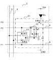
図7は、図1の表示装置等の本発明に係る表示装置に好適に用いられる有機EL素子を含む画素回路の一例である。 FIG. 7 is an example of a pixel circuit including an organic EL element preferably used in the display device according to the present invention such as the display device of FIG.
制御信号P1を伝達する制御線は、トランジスタTr1のゲートに接続され、データ電圧Vdataを供給するデータ線は、トランジスタTr1のソースに接続されている。オートゼロ期間を決める制御信号P2を伝達する制御線は、トランジスタTr3のゲートに接続され、発光期間を制御する制御信号P3を伝達する制御線は、トランジスタTr4のゲートに接続されている。+VCC配線は、駆動トランジスタTr2のソース及び容量C1の一端に接続されている。有機EL素子のアノードは、トランジスタTr4のドレインに接続され、有機ELのカソードは、CGND配線に接続されている。トランジスタTr4のソースは、駆動トランジスタTr2及びトランジスタTr3のドレインに接続されている。トランジスタTr1のドレインは、容量C2の1つの端子に接続され、容量C2のもう1つの端子は、駆動トランジスタTr2のゲート、トランジスタTr3のソース、及び容量C1のVccに接続されていないほうの端子が接続されている。 The control line for transmitting the control signal P1 is connected to the gate of the transistor Tr1, and the data line for supplying the data voltage Vdata is connected to the source of the transistor Tr1. A control line for transmitting the control signal P2 for determining the auto-zero period is connected to the gate of the transistor Tr3, and a control line for transmitting the control signal P3 for controlling the light emission period is connected to the gate of the transistor Tr4. The + VCC wiring is connected to the source of the driving transistor Tr2 and one end of the capacitor C1. The anode of the organic EL element is connected to the drain of the transistor Tr4, and the cathode of the organic EL is connected to the CGND wiring. The source of the transistor Tr4 is connected to the drains of the drive transistor Tr2 and the transistor Tr3. The drain of the transistor Tr1 is connected to one terminal of the capacitor C2, and the other terminal of the capacitor C2 is connected to the gate of the driving transistor Tr2, the source of the transistor Tr3, and the terminal not connected to Vcc of the capacitor C1. It is connected.
図7において、画素回路は3つのNMOSトランジスタ(Tr1、Tr3、Tr4)、駆動トランジスタであるPMOSトランジスタ(Tr2)、2つの容量C1及びC2、有機EL素子(OLED)、データ線、制御線(P1、P2、P3)を有する。さらに、画素回路は+VCC配線及びGND配線を有する。 In FIG. 7, the pixel circuit includes three NMOS transistors (Tr1, Tr3, Tr4), a PMOS transistor (Tr2) as a driving transistor, two capacitors C1 and C2, an organic EL element (OLED), a data line, and a control line (P1). , P2, P3). Further, the pixel circuit has a + VCC wiring and a GND wiring.
図7では、データ電圧Vdataを供給するデータ線は、参照電圧を供給する参照電圧線としての働きも兼ねている参照電圧線兼データ線である。なお、参照電圧線とデータ線を別々の配線としても良い。 In FIG. 7, the data line for supplying the data voltage Vdata is a reference voltage line / data line that also functions as a reference voltage line for supplying the reference voltage. The reference voltage line and the data line may be separate wirings.
容量C1はデータ線の信号電圧を保持するための保持容量、容量C2はデータ線の電圧信号を容量C1と駆動トランジスタTr2のゲートに伝えるための結合容量である。 The capacitor C1 is a holding capacitor for holding the signal voltage of the data line, and the capacitor C2 is a coupling capacitor for transferring the voltage signal of the data line to the capacitor C1 and the gate of the driving transistor Tr2.
駆動トランジスタTr2は、有機EL素子に電流を供給する駆動トランジスタである。図7では、駆動トランジスタTr2としてPMOSを使用している。 The drive transistor Tr2 is a drive transistor that supplies current to the organic EL element. In FIG. 7, a PMOS is used as the drive transistor Tr2.
トランジスタTr1はデータ線と容量C2のデータ線側の電極の間を接続するスイッチとして機能する。トランジスタTr3は駆動トランジスタTr2のドレインとゲートの間を短絡するスイッチ、トランジスタTr4は駆動トランジスタTr2から有機EL素子ELに流れる電流径路を遮断するスイッチである。 The transistor Tr1 functions as a switch that connects between the data line and the electrode on the data line side of the capacitor C2. The transistor Tr3 is a switch that short-circuits between the drain and gate of the drive transistor Tr2, and the transistor Tr4 is a switch that blocks a current path flowing from the drive transistor Tr2 to the organic EL element EL.
制御信号P1−P3は3つのNMOSスイッチングトランジスタTr1、Tr3、Tr4の動作を制御する。 Control signals P1-P3 control the operation of the three NMOS switching transistors Tr1, Tr3, Tr4.
図8は、図7の画素回路の動作を示すタイミングチャートである。 FIG. 8 is a timing chart showing the operation of the pixel circuit of FIG.
図8のタイミングチャートに示されているように、図7の回路は1つの行(i番目の行とする)について(A)プリチャージ、(B)オートゼロ、(C)サンプリング、(D)発光の4つの期間がある。 As shown in the timing chart of FIG. 8, the circuit of FIG. 7 has (A) precharge, (B) auto-zero, (C) sampling, and (D) light emission for one row (assumed to be the i-th row). There are four periods.
まず(A)のプリチャージ期間で、P1−P3がすべてH(High)になる。この期間、スイッチングトランジスタTr1、Tr3、Tr4はすべてオンになり、駆動トランジスタTr2がダイオード接続された状態で有機EL素子ELに電流が流れる。またデータ線には参照電圧Vrefがかかっている。この結果、Tr2のゲート電圧は低いレベルにリセットされる。 First, in the precharge period of (A), all of P1-P3 become H (High). During this period, the switching transistors Tr1, Tr3, Tr4 are all turned on, and a current flows through the organic EL element EL in a state where the driving transistor Tr2 is diode-connected. A reference voltage Vref is applied to the data line. As a result, the gate voltage of Tr2 is reset to a low level.
(B)のオートゼロ期間は、Tr4がオフになるので、Tr2のドレイン電流はTr3を通ってC1とC2の電荷を放電する。放電が進むにつれてTr2のゲート電位が上昇し、十分長い時間の経過後にはTr2が非導通状態になる。このときのTr2のゲートはVccから閾値電圧Vthだけ下がった電位になる。 During the auto-zero period (B), Tr4 is turned off, so that the drain current of Tr2 discharges the charges of C1 and C2 through Tr3. As the discharge proceeds, the gate potential of Tr2 rises, and after a sufficiently long time, Tr2 becomes non-conductive. At this time, the gate of Tr2 becomes a potential lower than Vcc by the threshold voltage Vth.
(C)のサンプリング期間は、Tr3がオフになるとともにデータ線にデータ電圧V(i)が印加される。VrefとV(i)の電圧差が、容量C1とC2の比に応じた割合でTr2のゲート電位を降下させ、降下分に応じた深さでTr2が導通状態になる。サンプリング期間の終了時にTr1がオフになり、この導通状態のTr2のゲート電圧がC2の端子間電圧として保持される。 During the sampling period (C), Tr3 is turned off and the data voltage V (i) is applied to the data line. The voltage difference between Vref and V (i) causes the gate potential of Tr2 to drop at a rate corresponding to the ratio between the capacitors C1 and C2, and Tr2 becomes conductive at a depth corresponding to the drop. At the end of the sampling period, Tr1 is turned off, and the gate voltage of Tr2 in the conductive state is held as the C2 terminal voltage.
(D)の期間は、Tr4がオンとなり、C2に保持されたTr2の導通状態に応じて、Tr2から有機EL素子ELに電流が流れ、有機EL素子ELが発光する。 During the period (D), Tr4 is turned on, and current flows from Tr2 to the organic EL element EL according to the conducting state of Tr2 held in C2, and the organic EL element EL emits light.
このように、Tr3とTr4とは、駆動トランジスタTr2のゲート初期電圧を設定する機能を持っているので、実施例1のゲート電圧設定回路22を構成する。ゲート電圧設定回路22は、これらのスイッチを制御する制御線P2とP3、それらに制御信号を送る回路(図1の行制御回路3)も含んでいるとみなしてもよい。また、設定されるゲート初期電圧Vg1は、今の場合、Vcc−Vthである。
Thus, since Tr3 and Tr4 have a function of setting the gate initial voltage of the drive transistor Tr2, the gate
また、トランジスタTr1とデータ線8と図1の列制御回路が、容量端電圧設定回路23を構成する。
Further, the transistor Tr1, the
本実施例では、図8(c)のようにオートゼロ期間を短くして、ゲート電位がVcc−Vthに収束する前にオートゼロ期間を終了する。通常モードでは、ゲート電位がVcc−Vthに収束するまで、あるいはその電位に近い値になるまでオートゼロ期間を維持する。高輝度モードでは、オートゼロ期間が通常モードより短いので、ゲート電位はVcc−Vthより低い電位にとどまる。 In this embodiment, the auto-zero period is shortened as shown in FIG. 8C, and the auto-zero period ends before the gate potential converges to Vcc-Vth. In the normal mode, the auto-zero period is maintained until the gate potential converges to Vcc-Vth or becomes a value close to the potential. In the high luminance mode, since the auto zero period is shorter than that in the normal mode, the gate potential remains lower than Vcc−Vth.
ゲート初期電圧が低いと、サンプリング期間後のゲート電圧もその分だけ低くなる。したがって、ゲート初期電圧の変化は、参照電圧の変化と同じ効果を生じる。すなわち、ゲート初期電圧が下がると、データに応じて定まるゲート電圧も全体に低いレベルにシフトするので、Vrefを低くしたのと同じ効果を生じ、高輝度モードが実現される。 If the gate initial voltage is low, the gate voltage after the sampling period also decreases accordingly. Therefore, the change in the initial gate voltage has the same effect as the change in the reference voltage. That is, when the gate initial voltage is lowered, the gate voltage determined according to the data is also shifted to a lower level as a whole, so that the same effect as when Vref is lowered is produced and the high luminance mode is realized.
オートゼロ期間の調節は、表示装置のコントローラ(不図示)または行制御回路3に設けられる。表示装置の使用者が切り換えスイッチを高輝度モード側にすると、その信号がコントローラまたは行制御回路3に送られ、制御信号P2のパルス幅を短くする。
The adjustment of the auto-zero period is provided in a controller (not shown) or the
オートゼロ期間の長さの変更と、参照電圧の変更は独立しており、いずれか一方の調節で高輝度モードを造ることができる。しかし、オートゼロ期間の長さを変更し、かつ、参照電圧を変更することで、より大きな最大輝度の上昇効果を得ることも可能である。 The change in the length of the auto-zero period and the change in the reference voltage are independent, and a high brightness mode can be created by adjusting either one. However, it is also possible to obtain a larger maximum brightness increase effect by changing the length of the auto-zero period and changing the reference voltage.
本実施例によれば、オートゼロ期間を変更することで容易に有機EL素子の輝度を制御できる。データ電圧や参照電圧は変更する必要はない。 According to the present embodiment, the luminance of the organic EL element can be easily controlled by changing the auto-zero period. There is no need to change the data voltage or the reference voltage.
1 画素、2 画素回路、3 行制御回路、4 列制御回路、5、6、7 制御線、8 データ線、9 参照電圧線、EL 有機EL素子、21 電流供給回路部、22 ゲート電圧設定回路、23 容量端電圧設定回路 1 pixel, 2 pixel circuit, 3 row control circuit, 4 column control circuit, 5, 6, 7 control line, 8 data line, 9 reference voltage line, EL organic EL element, 21 current supply circuit unit, 22 gate voltage setting circuit , 23 Capacitor end voltage setting circuit
Claims (4)
ソースが電源に接続され、ドレインが前記発光素子に電流を供給するトランジスタと、
前記トランジスタのゲートに一端が接続された容量と、
前記トランジスタのゲートに切り離し可能に接続され、前記トランジスタのゲートを初期電圧に設定するゲート電圧設定回路と、
前記容量の他端に接続され、前記容量の前記他端の電圧を、画像情報に対応したデータ電圧と画像情報によらない一定の参照電圧のいずれかに設定する容量端電圧設定回路と、を備え、
前記ゲート電圧設定回路が前記トランジスタのゲート電圧を前記初期電圧に設定するとともに、前記容量端電圧設定回路が、前記容量の前記他端の電圧を、前記データ電圧および前記参照電圧のうちのいずれか一方に設定し、
前記トランジスタのゲート電圧を前記初期電圧に設定した後、前記容量の前記他端の電圧を、前記設定された一方の電圧から他方の電圧に切り替えることにより、前記トランジスタのゲート電圧が前記データ電圧に依存する書き込み電圧に設定され、
前記書き込み電圧によって定まる電流を前記発光素子に供給する表示装置であって、
前記ゲート電圧設定回路が、前記トランジスタのドレインから前記発光素子に供給される電流を遮断する手段と、前記トランジスタのゲート−ドレイン間を短絡する短絡スイッチとを含んでおり、
前記短絡スイッチによる前記ゲート−ドレイン間の短絡を終了するタイミングを変化させて前記初期電圧を変化させることにより、前記発光素子に流れる電流が前記データ電圧に依存して変動する範囲をシフトさせる調整手段を有することを特徴とする表示装置。 A light emitting element that emits light when a current flows;
A transistor having a source connected to a power source and a drain supplying current to the light emitting element;
A capacitor having one end connected to the gate of the transistor;
A gate voltage setting circuit that is detachably connected to the gate of the transistor and sets the gate of the transistor to an initial voltage;
A capacitor end voltage setting circuit that is connected to the other end of the capacitor and sets a voltage at the other end of the capacitor to either a data voltage corresponding to image information or a constant reference voltage not depending on image information; Prepared,
The gate voltage setting circuit sets the gate voltage of the transistor to the initial voltage, and the capacitor end voltage setting circuit sets the voltage at the other end of the capacitor to one of the data voltage and the reference voltage. Set to one,
After setting the gate voltage of the transistor to the initial voltage, the gate voltage of the transistor is changed to the data voltage by switching the voltage at the other end of the capacitor from the set one voltage to the other voltage. Depending on the write voltage,
A display device for supplying a current determined by the writing voltage to the light emitting element,
The gate voltage setting circuit includes means for interrupting a current supplied from the drain of the transistor to the light emitting element, and a short-circuit switch for short-circuiting between the gate and drain of the transistor;
Wherein by the short-circuit switch gate - by varying the initial voltage by changing the timing to terminate the short circuit between the drain, the adjustment for shifting the range the current flowing in the light emitting element varies depending on the data voltage A display device comprising means.
ソースが電源に接続され、ドレインから前記発光素子に電流を供給するトランジスタと、前記トランジスタのゲートに一端が接続された容量と、
前記トランジスタのゲートに切り離し可能に接続され、前記トランジスタのゲート電圧を初期電圧に設定するゲート電圧設定回路と、
前記容量の他端に接続され、前記容量の前記他端の電圧を、画像情報に対応したデータ電圧と画像情報によらない一定の参照電圧のいずれかに設定する容量端電圧設定回路と、
を備えた表示装置の駆動方法であって、
前記ゲート電圧設定回路が、前記トランジスタのドレインから前記発光素子に供給される電流を遮断する手段と、前記トランジスタのゲート−ドレイン間を短絡する短絡スイッチとを含んでおり、
(1)前記ゲート電圧設定回路が、前記トランジスタのゲート電圧を前記初期電圧に設定する工程と、
(2)前記容量端電圧設定回路が、前記容量の前記他端の電圧を前記データ電圧および前記参照電圧のうちのいずれか一方に設定する工程と、
(3)前記トランジスタのゲート電圧を前記初期電圧に設定した後、前記容量の前記他端の電圧を前記(2)で設定された一方の電圧から他方の電圧に切り替えることにより、前記トランジスタのゲート電圧を前記データ電圧に依存する書き込み電圧に設定する工程と、
(4)前記書き込み電圧に応じた電流を前記発光素子に供給する工程と、
を有し、前記短絡スイッチによる前記ゲート−ドレイン間の短絡を終了するタイミングを変化させて前記初期電圧を変化させることにより、前記発光素子に流れる電流が前記データ電圧に依存して変動する範囲をシフトさせることを特徴とする表示装置の駆動方法。 A light emitting element that emits light when a current flows;
A transistor having a source connected to a power supply and supplying a current from a drain to the light emitting element; a capacitor having one end connected to the gate of the transistor;
A gate voltage setting circuit that is detachably connected to the gate of the transistor and sets the gate voltage of the transistor to an initial voltage;
Connected to the other end of the capacitor, the voltage of the other end of the capacitor, and the capacitor terminal voltage setting circuit for setting to one of the constant reference voltage which does not depend on the data voltage and the image information corresponding to image information,
A driving method of a display device comprising:
The gate voltage setting circuit includes means for interrupting a current supplied from the drain of the transistor to the light emitting element, and a short-circuit switch for short-circuiting between the gate and drain of the transistor;
(1) the gate voltage setting circuit setting the gate voltage of the transistor to the initial voltage;
(2) a step wherein the capacitor terminal voltage setting circuit sets the voltage of the other end of the capacitor to one of said data voltage and the reference voltage,
(3) After the gate voltage of the transistor is set to the initial voltage, by switching the voltage of the other end of the capacitor to the voltage of the other side from one of the voltage set by the (2), said transistor Setting a gate voltage to a write voltage depending on the data voltage ;
(4) and a current corresponding to the write voltage as engineering you supplied to the light emitting element,
Has the gate by the short-circuit switch - by varying the initial voltage by changing the timing to terminate the short circuit between the drain, the range of current flowing to the light emitting element varies depending on the data voltage The display device is driven by a shift method.
Priority Applications (3)
| Application Number | Priority Date | Filing Date | Title |
|---|---|---|---|
| JP2009154728A JP5284198B2 (en) | 2009-06-30 | 2009-06-30 | Display device and driving method thereof |
| US12/795,137 US20100328365A1 (en) | 2009-06-30 | 2010-06-07 | Semiconductor device |
| CN201010215149.3A CN101937645A (en) | 2009-06-30 | 2010-06-25 | Semiconductor device and driving method thereof |
Applications Claiming Priority (1)
| Application Number | Priority Date | Filing Date | Title |
|---|---|---|---|
| JP2009154728A JP5284198B2 (en) | 2009-06-30 | 2009-06-30 | Display device and driving method thereof |
Publications (3)
| Publication Number | Publication Date |
|---|---|
| JP2011013256A JP2011013256A (en) | 2011-01-20 |
| JP2011013256A5 JP2011013256A5 (en) | 2013-02-28 |
| JP5284198B2 true JP5284198B2 (en) | 2013-09-11 |
Family
ID=43380224
Family Applications (1)
| Application Number | Title | Priority Date | Filing Date |
|---|---|---|---|
| JP2009154728A Expired - Fee Related JP5284198B2 (en) | 2009-06-30 | 2009-06-30 | Display device and driving method thereof |
Country Status (3)
| Country | Link |
|---|---|
| US (1) | US20100328365A1 (en) |
| JP (1) | JP5284198B2 (en) |
| CN (1) | CN101937645A (en) |
Families Citing this family (23)
| Publication number | Priority date | Publication date | Assignee | Title |
|---|---|---|---|---|
| JP5495510B2 (en) * | 2007-06-19 | 2014-05-21 | キヤノン株式会社 | Display device and electronic apparatus using the same |
| JP2009014836A (en) * | 2007-07-02 | 2009-01-22 | Canon Inc | Active matrix type display and driving method therefor |
| US8497885B2 (en) * | 2007-08-21 | 2013-07-30 | Canon Kabushiki Karsha | Display apparatus and drive method thereof |
| JP2009080272A (en) * | 2007-09-26 | 2009-04-16 | Canon Inc | Active matrix type display device |
| JP2009109641A (en) * | 2007-10-29 | 2009-05-21 | Canon Inc | Driving circuit and active matrix type display device |
| JP2011013415A (en) * | 2009-07-01 | 2011-01-20 | Canon Inc | Active matrix type display apparatus |
| JP2011028135A (en) * | 2009-07-29 | 2011-02-10 | Canon Inc | Display device and driving method of the same |
| JP5409511B2 (en) * | 2010-05-20 | 2014-02-05 | 株式会社日立ハイテクノロジーズ | Electron microscope and method of adjusting optical axis of electron microscope |
| JP6124573B2 (en) | 2011-12-20 | 2017-05-10 | キヤノン株式会社 | Display device |
| JP5821685B2 (en) | 2012-02-22 | 2015-11-24 | セイコーエプソン株式会社 | Electro-optical device and electronic apparatus |
| KR101411619B1 (en) | 2012-09-27 | 2014-06-25 | 엘지디스플레이 주식회사 | Pixel circuit and method for driving thereof, and organic light emitting display device using the same |
| KR102068263B1 (en) * | 2013-07-10 | 2020-01-21 | 삼성디스플레이 주식회사 | Organic light emitting display device and method of driving the same |
| JP6478518B2 (en) | 2014-08-11 | 2019-03-06 | キヤノン株式会社 | Light emitting device and image forming apparatus |
| KR102218642B1 (en) * | 2014-11-27 | 2021-02-23 | 삼성디스플레이 주식회사 | Display device and method of driving a display device |
| KR102288961B1 (en) * | 2014-12-24 | 2021-08-12 | 엘지디스플레이 주식회사 | Rganic light emitting display panel, organic light emitting display device, and the method for the organic light emitting display device |
| JP6052365B2 (en) * | 2015-10-02 | 2016-12-27 | セイコーエプソン株式会社 | Electro-optical device and electronic apparatus |
| US10297191B2 (en) | 2016-01-29 | 2019-05-21 | Samsung Display Co., Ltd. | Dynamic net power control for OLED and local dimming LCD displays |
| US11381149B2 (en) * | 2017-09-25 | 2022-07-05 | Shindengen Electric Manufacturing Co., Ltd. | Switching element control circuit and power module |
| CN108877674A (en) * | 2018-07-27 | 2018-11-23 | 京东方科技集团股份有限公司 | A kind of pixel circuit and its driving method, display device |
| CN109712568B (en) * | 2019-02-27 | 2021-04-23 | 京东方科技集团股份有限公司 | Pixel driving circuit and driving method thereof, display panel and display device |
| CN111402798B (en) * | 2020-03-30 | 2021-12-21 | 合肥鑫晟光电科技有限公司 | Pixel driving circuit, control method thereof and display device |
| CN112309320A (en) * | 2020-11-05 | 2021-02-02 | 重庆惠科金渝光电科技有限公司 | Display panel drive circuit and display device |
| JP2023114122A (en) * | 2022-02-04 | 2023-08-17 | 有限会社大平技研 | display system |
Family Cites Families (65)
| Publication number | Priority date | Publication date | Assignee | Title |
|---|---|---|---|---|
| JPH0555881A (en) * | 1991-08-27 | 1993-03-05 | Toshiba Corp | Delay circuit |
| US6078318A (en) * | 1995-04-27 | 2000-06-20 | Canon Kabushiki Kaisha | Data transfer method, display driving circuit using the method, and image display apparatus |
| JP3062418B2 (en) * | 1995-06-02 | 2000-07-10 | キヤノン株式会社 | Display device, display system, and display control method |
| US6188378B1 (en) * | 1995-06-02 | 2001-02-13 | Canon Kabushiki Kaisha | Display apparatus, display system, and display control method for display system |
| JP3503727B2 (en) * | 1996-09-06 | 2004-03-08 | パイオニア株式会社 | Driving method of plasma display panel |
| GB9803441D0 (en) * | 1998-02-18 | 1998-04-15 | Cambridge Display Tech Ltd | Electroluminescent devices |
| GB9812742D0 (en) * | 1998-06-12 | 1998-08-12 | Philips Electronics Nv | Active matrix electroluminescent display devices |
| JP2001159877A (en) * | 1999-09-20 | 2001-06-12 | Sharp Corp | Matrix type image display device |
| US6587086B1 (en) * | 1999-10-26 | 2003-07-01 | Semiconductor Energy Laboratory Co., Ltd. | Electro-optical device |
| JP3301422B2 (en) * | 1999-11-08 | 2002-07-15 | 日本電気株式会社 | Display driving method and circuit thereof |
| SG114502A1 (en) * | 2000-10-24 | 2005-09-28 | Semiconductor Energy Lab | Light emitting device and method of driving the same |
| KR100370286B1 (en) * | 2000-12-29 | 2003-01-29 | 삼성에스디아이 주식회사 | circuit of electroluminescent display pixel for voltage driving |
| WO2002075709A1 (en) * | 2001-03-21 | 2002-09-26 | Canon Kabushiki Kaisha | Circuit for driving active-matrix light-emitting element |
| US6661180B2 (en) * | 2001-03-22 | 2003-12-09 | Semiconductor Energy Laboratory Co., Ltd. | Light emitting device, driving method for the same and electronic apparatus |
| EP3716257B1 (en) * | 2001-09-07 | 2021-01-20 | Joled Inc. | El display panel, method of driving the same, and el display device |
| SG120075A1 (en) * | 2001-09-21 | 2006-03-28 | Semiconductor Energy Lab | Semiconductor device |
| JP2003173163A (en) * | 2001-09-27 | 2003-06-20 | Sharp Corp | Display device |
| US7876294B2 (en) * | 2002-03-05 | 2011-01-25 | Nec Corporation | Image display and its control method |
| KR100649243B1 (en) * | 2002-03-21 | 2006-11-24 | 삼성에스디아이 주식회사 | Organic electroluminescent display and driving method thereof |
| JP4416456B2 (en) * | 2002-09-02 | 2010-02-17 | キヤノン株式会社 | Electroluminescence device |
| JP3832415B2 (en) * | 2002-10-11 | 2006-10-11 | ソニー株式会社 | Active matrix display device |
| JP2004191752A (en) * | 2002-12-12 | 2004-07-08 | Seiko Epson Corp | Electrooptical device, driving method for electrooptical device, and electronic equipment |
| US7253812B2 (en) * | 2003-02-12 | 2007-08-07 | Sanyo Electric Co., Ltd. | El display driver and El display |
| JP3950845B2 (en) * | 2003-03-07 | 2007-08-01 | キヤノン株式会社 | Driving circuit and evaluation method thereof |
| WO2004086348A1 (en) * | 2003-03-25 | 2004-10-07 | Canon Kabushiki Kaisha | Driving method of display apparatus in which a handwriting can be overweitten on the displayed image |
| JP2004341144A (en) * | 2003-05-15 | 2004-12-02 | Hitachi Ltd | Image display device |
| JP4838498B2 (en) * | 2003-05-21 | 2011-12-14 | キヤノン株式会社 | Display device |
| JP4062179B2 (en) * | 2003-06-04 | 2008-03-19 | ソニー株式会社 | Pixel circuit, display device, and driving method of pixel circuit |
| KR100515351B1 (en) * | 2003-07-08 | 2005-09-15 | 삼성에스디아이 주식회사 | Display panel, light emitting display device using the panel and driving method thereof |
| GB0319963D0 (en) * | 2003-08-27 | 2003-09-24 | Koninkl Philips Electronics Nv | Display device |
| JP4054794B2 (en) * | 2003-12-04 | 2008-03-05 | キヤノン株式会社 | DRIVE DEVICE, DISPLAY DEVICE, AND RECORDING DEVICE |
| US7605899B2 (en) * | 2003-12-05 | 2009-10-20 | Canon Kabushiki Kaisha | Electrophoretic dispersion liquid and electrophoretic display device |
| US7608861B2 (en) * | 2004-06-24 | 2009-10-27 | Canon Kabushiki Kaisha | Active matrix type display having two transistors of opposite conductivity acting as a single switch for the driving transistor of a display element |
| KR100748308B1 (en) * | 2004-09-15 | 2007-08-09 | 삼성에스디아이 주식회사 | Pixel and light emitting display having the same and driving method thereof |
| KR100606416B1 (en) * | 2004-11-17 | 2006-07-31 | 엘지.필립스 엘시디 주식회사 | Driving Apparatus And Method For Organic Light-Emitting Diode |
| JP4438066B2 (en) * | 2004-11-26 | 2010-03-24 | キヤノン株式会社 | Active matrix display device and current programming method thereof |
| JP4438067B2 (en) * | 2004-11-26 | 2010-03-24 | キヤノン株式会社 | Active matrix display device and current programming method thereof |
| JP4438069B2 (en) * | 2004-12-03 | 2010-03-24 | キヤノン株式会社 | Current programming device, active matrix display device, and current programming method thereof |
| JP2006215296A (en) * | 2005-02-04 | 2006-08-17 | Sony Corp | Display device and pixel driving method |
| JP2006285116A (en) * | 2005-04-05 | 2006-10-19 | Eastman Kodak Co | Driving circuit |
| JP4752315B2 (en) * | 2005-04-19 | 2011-08-17 | セイコーエプソン株式会社 | Electronic circuit, driving method thereof, electro-optical device, and electronic apparatus |
| KR100639007B1 (en) * | 2005-05-26 | 2006-10-25 | 삼성에스디아이 주식회사 | Light emitting display and driving method thereof |
| US8044891B2 (en) * | 2005-08-05 | 2011-10-25 | Chimei Innolux Corporation | Systems and methods for providing threshold voltage compensation of pixels |
| WO2007029374A1 (en) * | 2005-09-01 | 2007-03-15 | Sharp Kabushiki Kaisha | Display device |
| US7872617B2 (en) * | 2005-10-12 | 2011-01-18 | Canon Kabushiki Kaisha | Display apparatus and method for driving the same |
| JP4923527B2 (en) * | 2005-11-14 | 2012-04-25 | ソニー株式会社 | Display device and driving method thereof |
| JP2007271969A (en) * | 2006-03-31 | 2007-10-18 | Canon Inc | Color display device and active matrix device |
| JP5058505B2 (en) * | 2006-03-31 | 2012-10-24 | キヤノン株式会社 | Display device |
| US8325118B2 (en) * | 2006-05-30 | 2012-12-04 | Sharp Kabushiki Kaisha | Electric current driving type display device |
| KR101245218B1 (en) * | 2006-06-22 | 2013-03-19 | 엘지디스플레이 주식회사 | Organic light emitting diode display |
| JP2008009276A (en) * | 2006-06-30 | 2008-01-17 | Canon Inc | Display device and information processing device using the same |
| KR101279117B1 (en) * | 2006-06-30 | 2013-06-26 | 엘지디스플레이 주식회사 | OLED display and drive method thereof |
| JP4964527B2 (en) * | 2006-07-24 | 2012-07-04 | エルジー ディスプレイ カンパニー リミテッド | Driving method of image display device |
| JP5240542B2 (en) * | 2006-09-25 | 2013-07-17 | カシオ計算機株式会社 | Display driving device and driving method thereof, and display device and driving method thereof |
| JP5495510B2 (en) * | 2007-06-19 | 2014-05-21 | キヤノン株式会社 | Display device and electronic apparatus using the same |
| JP2009014836A (en) * | 2007-07-02 | 2009-01-22 | Canon Inc | Active matrix type display and driving method therefor |
| JP2009037123A (en) * | 2007-08-03 | 2009-02-19 | Canon Inc | Active matrix display device and its driving method |
| US8497885B2 (en) * | 2007-08-21 | 2013-07-30 | Canon Kabushiki Karsha | Display apparatus and drive method thereof |
| US20090066615A1 (en) * | 2007-09-11 | 2009-03-12 | Canon Kabushiki Kaisha | Display apparatus and driving method thereof |
| JP2009080272A (en) * | 2007-09-26 | 2009-04-16 | Canon Inc | Active matrix type display device |
| JP2009109641A (en) * | 2007-10-29 | 2009-05-21 | Canon Inc | Driving circuit and active matrix type display device |
| JP2009128601A (en) * | 2007-11-22 | 2009-06-11 | Canon Inc | Display device and integrated circuit |
| JP2010122355A (en) * | 2008-11-18 | 2010-06-03 | Canon Inc | Display apparatus and camera |
| JP2011013415A (en) * | 2009-07-01 | 2011-01-20 | Canon Inc | Active matrix type display apparatus |
| JP2011028135A (en) * | 2009-07-29 | 2011-02-10 | Canon Inc | Display device and driving method of the same |
-
2009
- 2009-06-30 JP JP2009154728A patent/JP5284198B2/en not_active Expired - Fee Related
-
2010
- 2010-06-07 US US12/795,137 patent/US20100328365A1/en not_active Abandoned
- 2010-06-25 CN CN201010215149.3A patent/CN101937645A/en active Pending
Also Published As
| Publication number | Publication date |
|---|---|
| US20100328365A1 (en) | 2010-12-30 |
| JP2011013256A (en) | 2011-01-20 |
| CN101937645A (en) | 2011-01-05 |
Similar Documents
| Publication | Publication Date | Title |
|---|---|---|
| JP5284198B2 (en) | Display device and driving method thereof | |
| EP2255354B1 (en) | Oled display panel with pwm control | |
| TWI417840B (en) | Pixel circuit, active matrix organic light emitting diode (oled) display and driving method for pixel circuit | |
| JP5096103B2 (en) | Display device | |
| EP1318499A2 (en) | Display apparatus with active matrix type display panel | |
| US11551606B2 (en) | LED driving circuit, display panel, and pixel driving device | |
| US20120069059A1 (en) | Organic Light Emitting Diode Display Device and Low Power Driving Method Thereof | |
| US20090167644A1 (en) | Resetting drive transistors in electronic displays | |
| JP2011191449A (en) | Image display device | |
| KR20110139764A (en) | Display device using capacitor coupled light emission control transitors | |
| US9165508B2 (en) | Display apparatus using reference voltage line for parasitic capacitance, electronic apparatus using the display apparatus and driving method of the display apparatus | |
| JP2009258275A (en) | Display device and output buffer circuit | |
| JP2005134880A (en) | Image display apparatus, driving method thereof, and precharge voltage setting method | |
| US11049474B2 (en) | Display device | |
| JP2009080272A (en) | Active matrix type display device | |
| US20160232843A1 (en) | Display device | |
| US7427970B2 (en) | Circuit for driving light emitting element and current-control-type light-emitting display | |
| CN112470210A (en) | Clock and voltage generating circuit and display device including the same | |
| US20130293527A1 (en) | Display device, method of driving display device, and electronic apparatus | |
| CN101140733A (en) | Driver circuit having electromechanical excitation light dipolar body and driving method thereof | |
| JP2009244411A (en) | Display apparatus and driving method thereof | |
| KR20090073688A (en) | Luminescence dispaly and driving method thereof | |
| JP2010008987A (en) | Drive circuit | |
| KR20070002891A (en) | Unit for driving organic electroluminescence display device | |
| JP2007086328A (en) | Driving circuit and driving method of display device |
Legal Events
| Date | Code | Title | Description |
|---|---|---|---|
| A621 | Written request for application examination |
Free format text: JAPANESE INTERMEDIATE CODE: A621 Effective date: 20120627 |
|
| A521 | Request for written amendment filed |
Free format text: JAPANESE INTERMEDIATE CODE: A523 Effective date: 20130110 |
|
| A977 | Report on retrieval |
Free format text: JAPANESE INTERMEDIATE CODE: A971007 Effective date: 20130122 |
|
| A131 | Notification of reasons for refusal |
Free format text: JAPANESE INTERMEDIATE CODE: A131 Effective date: 20130205 |
|
| A521 | Request for written amendment filed |
Free format text: JAPANESE INTERMEDIATE CODE: A523 Effective date: 20130408 |
|
| TRDD | Decision of grant or rejection written | ||
| A01 | Written decision to grant a patent or to grant a registration (utility model) |
Free format text: JAPANESE INTERMEDIATE CODE: A01 Effective date: 20130430 |
|
| A61 | First payment of annual fees (during grant procedure) |
Free format text: JAPANESE INTERMEDIATE CODE: A61 Effective date: 20130529 |
|
| LAPS | Cancellation because of no payment of annual fees |