JP2004191752A - Electrooptical device, driving method for electrooptical device, and electronic equipment - Google Patents
Electrooptical device, driving method for electrooptical device, and electronic equipment Download PDFInfo
- Publication number
- JP2004191752A JP2004191752A JP2002360978A JP2002360978A JP2004191752A JP 2004191752 A JP2004191752 A JP 2004191752A JP 2002360978 A JP2002360978 A JP 2002360978A JP 2002360978 A JP2002360978 A JP 2002360978A JP 2004191752 A JP2004191752 A JP 2004191752A
- Authority
- JP
- Japan
- Prior art keywords
- data
- scanning line
- pixel
- current
- written
- Prior art date
- Legal status (The legal status is an assumption and is not a legal conclusion. Google has not performed a legal analysis and makes no representation as to the accuracy of the status listed.)
- Pending
Links
Images


Classifications
-
- G—PHYSICS
- G09—EDUCATION; CRYPTOGRAPHY; DISPLAY; ADVERTISING; SEALS
- G09G—ARRANGEMENTS OR CIRCUITS FOR CONTROL OF INDICATING DEVICES USING STATIC MEANS TO PRESENT VARIABLE INFORMATION
- G09G3/00—Control arrangements or circuits, of interest only in connection with visual indicators other than cathode-ray tubes
- G09G3/20—Control arrangements or circuits, of interest only in connection with visual indicators other than cathode-ray tubes for presentation of an assembly of a number of characters, e.g. a page, by composing the assembly by combination of individual elements arranged in a matrix no fixed position being assigned to or needed to be assigned to the individual characters or partial characters
- G09G3/22—Control arrangements or circuits, of interest only in connection with visual indicators other than cathode-ray tubes for presentation of an assembly of a number of characters, e.g. a page, by composing the assembly by combination of individual elements arranged in a matrix no fixed position being assigned to or needed to be assigned to the individual characters or partial characters using controlled light sources
- G09G3/30—Control arrangements or circuits, of interest only in connection with visual indicators other than cathode-ray tubes for presentation of an assembly of a number of characters, e.g. a page, by composing the assembly by combination of individual elements arranged in a matrix no fixed position being assigned to or needed to be assigned to the individual characters or partial characters using controlled light sources using electroluminescent panels
- G09G3/32—Control arrangements or circuits, of interest only in connection with visual indicators other than cathode-ray tubes for presentation of an assembly of a number of characters, e.g. a page, by composing the assembly by combination of individual elements arranged in a matrix no fixed position being assigned to or needed to be assigned to the individual characters or partial characters using controlled light sources using electroluminescent panels semiconductive, e.g. using light-emitting diodes [LED]
- G09G3/3208—Control arrangements or circuits, of interest only in connection with visual indicators other than cathode-ray tubes for presentation of an assembly of a number of characters, e.g. a page, by composing the assembly by combination of individual elements arranged in a matrix no fixed position being assigned to or needed to be assigned to the individual characters or partial characters using controlled light sources using electroluminescent panels semiconductive, e.g. using light-emitting diodes [LED] organic, e.g. using organic light-emitting diodes [OLED]
- G09G3/3225—Control arrangements or circuits, of interest only in connection with visual indicators other than cathode-ray tubes for presentation of an assembly of a number of characters, e.g. a page, by composing the assembly by combination of individual elements arranged in a matrix no fixed position being assigned to or needed to be assigned to the individual characters or partial characters using controlled light sources using electroluminescent panels semiconductive, e.g. using light-emitting diodes [LED] organic, e.g. using organic light-emitting diodes [OLED] using an active matrix
- G09G3/3233—Control arrangements or circuits, of interest only in connection with visual indicators other than cathode-ray tubes for presentation of an assembly of a number of characters, e.g. a page, by composing the assembly by combination of individual elements arranged in a matrix no fixed position being assigned to or needed to be assigned to the individual characters or partial characters using controlled light sources using electroluminescent panels semiconductive, e.g. using light-emitting diodes [LED] organic, e.g. using organic light-emitting diodes [OLED] using an active matrix with pixel circuitry controlling the current through the light-emitting element
- G09G3/3241—Control arrangements or circuits, of interest only in connection with visual indicators other than cathode-ray tubes for presentation of an assembly of a number of characters, e.g. a page, by composing the assembly by combination of individual elements arranged in a matrix no fixed position being assigned to or needed to be assigned to the individual characters or partial characters using controlled light sources using electroluminescent panels semiconductive, e.g. using light-emitting diodes [LED] organic, e.g. using organic light-emitting diodes [OLED] using an active matrix with pixel circuitry controlling the current through the light-emitting element the current through the light-emitting element being set using a data current provided by the data driver, e.g. by using a two-transistor current mirror
-
- G—PHYSICS
- G09—EDUCATION; CRYPTOGRAPHY; DISPLAY; ADVERTISING; SEALS
- G09G—ARRANGEMENTS OR CIRCUITS FOR CONTROL OF INDICATING DEVICES USING STATIC MEANS TO PRESENT VARIABLE INFORMATION
- G09G3/00—Control arrangements or circuits, of interest only in connection with visual indicators other than cathode-ray tubes
- G09G3/20—Control arrangements or circuits, of interest only in connection with visual indicators other than cathode-ray tubes for presentation of an assembly of a number of characters, e.g. a page, by composing the assembly by combination of individual elements arranged in a matrix no fixed position being assigned to or needed to be assigned to the individual characters or partial characters
- G09G3/22—Control arrangements or circuits, of interest only in connection with visual indicators other than cathode-ray tubes for presentation of an assembly of a number of characters, e.g. a page, by composing the assembly by combination of individual elements arranged in a matrix no fixed position being assigned to or needed to be assigned to the individual characters or partial characters using controlled light sources
- G09G3/30—Control arrangements or circuits, of interest only in connection with visual indicators other than cathode-ray tubes for presentation of an assembly of a number of characters, e.g. a page, by composing the assembly by combination of individual elements arranged in a matrix no fixed position being assigned to or needed to be assigned to the individual characters or partial characters using controlled light sources using electroluminescent panels
-
- G—PHYSICS
- G09—EDUCATION; CRYPTOGRAPHY; DISPLAY; ADVERTISING; SEALS
- G09G—ARRANGEMENTS OR CIRCUITS FOR CONTROL OF INDICATING DEVICES USING STATIC MEANS TO PRESENT VARIABLE INFORMATION
- G09G3/00—Control arrangements or circuits, of interest only in connection with visual indicators other than cathode-ray tubes
- G09G3/20—Control arrangements or circuits, of interest only in connection with visual indicators other than cathode-ray tubes for presentation of an assembly of a number of characters, e.g. a page, by composing the assembly by combination of individual elements arranged in a matrix no fixed position being assigned to or needed to be assigned to the individual characters or partial characters
- G09G3/2007—Display of intermediate tones
- G09G3/2011—Display of intermediate tones by amplitude modulation
-
- G—PHYSICS
- G09—EDUCATION; CRYPTOGRAPHY; DISPLAY; ADVERTISING; SEALS
- G09G—ARRANGEMENTS OR CIRCUITS FOR CONTROL OF INDICATING DEVICES USING STATIC MEANS TO PRESENT VARIABLE INFORMATION
- G09G3/00—Control arrangements or circuits, of interest only in connection with visual indicators other than cathode-ray tubes
- G09G3/20—Control arrangements or circuits, of interest only in connection with visual indicators other than cathode-ray tubes for presentation of an assembly of a number of characters, e.g. a page, by composing the assembly by combination of individual elements arranged in a matrix no fixed position being assigned to or needed to be assigned to the individual characters or partial characters
- G09G3/22—Control arrangements or circuits, of interest only in connection with visual indicators other than cathode-ray tubes for presentation of an assembly of a number of characters, e.g. a page, by composing the assembly by combination of individual elements arranged in a matrix no fixed position being assigned to or needed to be assigned to the individual characters or partial characters using controlled light sources
- G09G3/30—Control arrangements or circuits, of interest only in connection with visual indicators other than cathode-ray tubes for presentation of an assembly of a number of characters, e.g. a page, by composing the assembly by combination of individual elements arranged in a matrix no fixed position being assigned to or needed to be assigned to the individual characters or partial characters using controlled light sources using electroluminescent panels
- G09G3/32—Control arrangements or circuits, of interest only in connection with visual indicators other than cathode-ray tubes for presentation of an assembly of a number of characters, e.g. a page, by composing the assembly by combination of individual elements arranged in a matrix no fixed position being assigned to or needed to be assigned to the individual characters or partial characters using controlled light sources using electroluminescent panels semiconductive, e.g. using light-emitting diodes [LED]
- G09G3/3208—Control arrangements or circuits, of interest only in connection with visual indicators other than cathode-ray tubes for presentation of an assembly of a number of characters, e.g. a page, by composing the assembly by combination of individual elements arranged in a matrix no fixed position being assigned to or needed to be assigned to the individual characters or partial characters using controlled light sources using electroluminescent panels semiconductive, e.g. using light-emitting diodes [LED] organic, e.g. using organic light-emitting diodes [OLED]
- G09G3/3225—Control arrangements or circuits, of interest only in connection with visual indicators other than cathode-ray tubes for presentation of an assembly of a number of characters, e.g. a page, by composing the assembly by combination of individual elements arranged in a matrix no fixed position being assigned to or needed to be assigned to the individual characters or partial characters using controlled light sources using electroluminescent panels semiconductive, e.g. using light-emitting diodes [LED] organic, e.g. using organic light-emitting diodes [OLED] using an active matrix
- G09G3/3233—Control arrangements or circuits, of interest only in connection with visual indicators other than cathode-ray tubes for presentation of an assembly of a number of characters, e.g. a page, by composing the assembly by combination of individual elements arranged in a matrix no fixed position being assigned to or needed to be assigned to the individual characters or partial characters using controlled light sources using electroluminescent panels semiconductive, e.g. using light-emitting diodes [LED] organic, e.g. using organic light-emitting diodes [OLED] using an active matrix with pixel circuitry controlling the current through the light-emitting element
- G09G3/3241—Control arrangements or circuits, of interest only in connection with visual indicators other than cathode-ray tubes for presentation of an assembly of a number of characters, e.g. a page, by composing the assembly by combination of individual elements arranged in a matrix no fixed position being assigned to or needed to be assigned to the individual characters or partial characters using controlled light sources using electroluminescent panels semiconductive, e.g. using light-emitting diodes [LED] organic, e.g. using organic light-emitting diodes [OLED] using an active matrix with pixel circuitry controlling the current through the light-emitting element the current through the light-emitting element being set using a data current provided by the data driver, e.g. by using a two-transistor current mirror
- G09G3/325—Control arrangements or circuits, of interest only in connection with visual indicators other than cathode-ray tubes for presentation of an assembly of a number of characters, e.g. a page, by composing the assembly by combination of individual elements arranged in a matrix no fixed position being assigned to or needed to be assigned to the individual characters or partial characters using controlled light sources using electroluminescent panels semiconductive, e.g. using light-emitting diodes [LED] organic, e.g. using organic light-emitting diodes [OLED] using an active matrix with pixel circuitry controlling the current through the light-emitting element the current through the light-emitting element being set using a data current provided by the data driver, e.g. by using a two-transistor current mirror the data current flowing through the driving transistor during a setting phase, e.g. by using a switch for connecting the driving transistor to the data driver
-
- G—PHYSICS
- G09—EDUCATION; CRYPTOGRAPHY; DISPLAY; ADVERTISING; SEALS
- G09G—ARRANGEMENTS OR CIRCUITS FOR CONTROL OF INDICATING DEVICES USING STATIC MEANS TO PRESENT VARIABLE INFORMATION
- G09G3/00—Control arrangements or circuits, of interest only in connection with visual indicators other than cathode-ray tubes
- G09G3/20—Control arrangements or circuits, of interest only in connection with visual indicators other than cathode-ray tubes for presentation of an assembly of a number of characters, e.g. a page, by composing the assembly by combination of individual elements arranged in a matrix no fixed position being assigned to or needed to be assigned to the individual characters or partial characters
- G09G3/22—Control arrangements or circuits, of interest only in connection with visual indicators other than cathode-ray tubes for presentation of an assembly of a number of characters, e.g. a page, by composing the assembly by combination of individual elements arranged in a matrix no fixed position being assigned to or needed to be assigned to the individual characters or partial characters using controlled light sources
- G09G3/30—Control arrangements or circuits, of interest only in connection with visual indicators other than cathode-ray tubes for presentation of an assembly of a number of characters, e.g. a page, by composing the assembly by combination of individual elements arranged in a matrix no fixed position being assigned to or needed to be assigned to the individual characters or partial characters using controlled light sources using electroluminescent panels
- G09G3/32—Control arrangements or circuits, of interest only in connection with visual indicators other than cathode-ray tubes for presentation of an assembly of a number of characters, e.g. a page, by composing the assembly by combination of individual elements arranged in a matrix no fixed position being assigned to or needed to be assigned to the individual characters or partial characters using controlled light sources using electroluminescent panels semiconductive, e.g. using light-emitting diodes [LED]
- G09G3/3208—Control arrangements or circuits, of interest only in connection with visual indicators other than cathode-ray tubes for presentation of an assembly of a number of characters, e.g. a page, by composing the assembly by combination of individual elements arranged in a matrix no fixed position being assigned to or needed to be assigned to the individual characters or partial characters using controlled light sources using electroluminescent panels semiconductive, e.g. using light-emitting diodes [LED] organic, e.g. using organic light-emitting diodes [OLED]
- G09G3/3225—Control arrangements or circuits, of interest only in connection with visual indicators other than cathode-ray tubes for presentation of an assembly of a number of characters, e.g. a page, by composing the assembly by combination of individual elements arranged in a matrix no fixed position being assigned to or needed to be assigned to the individual characters or partial characters using controlled light sources using electroluminescent panels semiconductive, e.g. using light-emitting diodes [LED] organic, e.g. using organic light-emitting diodes [OLED] using an active matrix
- G09G3/3258—Control arrangements or circuits, of interest only in connection with visual indicators other than cathode-ray tubes for presentation of an assembly of a number of characters, e.g. a page, by composing the assembly by combination of individual elements arranged in a matrix no fixed position being assigned to or needed to be assigned to the individual characters or partial characters using controlled light sources using electroluminescent panels semiconductive, e.g. using light-emitting diodes [LED] organic, e.g. using organic light-emitting diodes [OLED] using an active matrix with pixel circuitry controlling the voltage across the light-emitting element
-
- G—PHYSICS
- G09—EDUCATION; CRYPTOGRAPHY; DISPLAY; ADVERTISING; SEALS
- G09G—ARRANGEMENTS OR CIRCUITS FOR CONTROL OF INDICATING DEVICES USING STATIC MEANS TO PRESENT VARIABLE INFORMATION
- G09G2300/00—Aspects of the constitution of display devices
- G09G2300/08—Active matrix structure, i.e. with use of active elements, inclusive of non-linear two terminal elements, in the pixels together with light emitting or modulating elements
- G09G2300/0809—Several active elements per pixel in active matrix panels
- G09G2300/0819—Several active elements per pixel in active matrix panels used for counteracting undesired variations, e.g. feedback or autozeroing
-
- G—PHYSICS
- G09—EDUCATION; CRYPTOGRAPHY; DISPLAY; ADVERTISING; SEALS
- G09G—ARRANGEMENTS OR CIRCUITS FOR CONTROL OF INDICATING DEVICES USING STATIC MEANS TO PRESENT VARIABLE INFORMATION
- G09G2300/00—Aspects of the constitution of display devices
- G09G2300/08—Active matrix structure, i.e. with use of active elements, inclusive of non-linear two terminal elements, in the pixels together with light emitting or modulating elements
- G09G2300/0809—Several active elements per pixel in active matrix panels
- G09G2300/0842—Several active elements per pixel in active matrix panels forming a memory circuit, e.g. a dynamic memory with one capacitor
- G09G2300/0852—Several active elements per pixel in active matrix panels forming a memory circuit, e.g. a dynamic memory with one capacitor being a dynamic memory with more than one capacitor
-
- G—PHYSICS
- G09—EDUCATION; CRYPTOGRAPHY; DISPLAY; ADVERTISING; SEALS
- G09G—ARRANGEMENTS OR CIRCUITS FOR CONTROL OF INDICATING DEVICES USING STATIC MEANS TO PRESENT VARIABLE INFORMATION
- G09G2300/00—Aspects of the constitution of display devices
- G09G2300/08—Active matrix structure, i.e. with use of active elements, inclusive of non-linear two terminal elements, in the pixels together with light emitting or modulating elements
- G09G2300/0809—Several active elements per pixel in active matrix panels
- G09G2300/0842—Several active elements per pixel in active matrix panels forming a memory circuit, e.g. a dynamic memory with one capacitor
- G09G2300/0861—Several active elements per pixel in active matrix panels forming a memory circuit, e.g. a dynamic memory with one capacitor with additional control of the display period without amending the charge stored in a pixel memory, e.g. by means of additional select electrodes
-
- G—PHYSICS
- G09—EDUCATION; CRYPTOGRAPHY; DISPLAY; ADVERTISING; SEALS
- G09G—ARRANGEMENTS OR CIRCUITS FOR CONTROL OF INDICATING DEVICES USING STATIC MEANS TO PRESENT VARIABLE INFORMATION
- G09G2310/00—Command of the display device
- G09G2310/02—Addressing, scanning or driving the display screen or processing steps related thereto
- G09G2310/0262—The addressing of the pixel, in a display other than an active matrix LCD, involving the control of two or more scan electrodes or two or more data electrodes, e.g. pixel voltage dependent on signals of two data electrodes
-
- G—PHYSICS
- G09—EDUCATION; CRYPTOGRAPHY; DISPLAY; ADVERTISING; SEALS
- G09G—ARRANGEMENTS OR CIRCUITS FOR CONTROL OF INDICATING DEVICES USING STATIC MEANS TO PRESENT VARIABLE INFORMATION
- G09G2320/00—Control of display operating conditions
- G09G2320/02—Improving the quality of display appearance
- G09G2320/0238—Improving the black level
-
- G—PHYSICS
- G09—EDUCATION; CRYPTOGRAPHY; DISPLAY; ADVERTISING; SEALS
- G09G—ARRANGEMENTS OR CIRCUITS FOR CONTROL OF INDICATING DEVICES USING STATIC MEANS TO PRESENT VARIABLE INFORMATION
- G09G2320/00—Control of display operating conditions
- G09G2320/02—Improving the quality of display appearance
- G09G2320/0247—Flicker reduction other than flicker reduction circuits used for single beam cathode-ray tubes
-
- G—PHYSICS
- G09—EDUCATION; CRYPTOGRAPHY; DISPLAY; ADVERTISING; SEALS
- G09G—ARRANGEMENTS OR CIRCUITS FOR CONTROL OF INDICATING DEVICES USING STATIC MEANS TO PRESENT VARIABLE INFORMATION
- G09G2320/00—Control of display operating conditions
- G09G2320/04—Maintaining the quality of display appearance
- G09G2320/043—Preventing or counteracting the effects of ageing
-
- G—PHYSICS
- G09—EDUCATION; CRYPTOGRAPHY; DISPLAY; ADVERTISING; SEALS
- G09G—ARRANGEMENTS OR CIRCUITS FOR CONTROL OF INDICATING DEVICES USING STATIC MEANS TO PRESENT VARIABLE INFORMATION
- G09G3/00—Control arrangements or circuits, of interest only in connection with visual indicators other than cathode-ray tubes
- G09G3/20—Control arrangements or circuits, of interest only in connection with visual indicators other than cathode-ray tubes for presentation of an assembly of a number of characters, e.g. a page, by composing the assembly by combination of individual elements arranged in a matrix no fixed position being assigned to or needed to be assigned to the individual characters or partial characters
- G09G3/2007—Display of intermediate tones
- G09G3/2018—Display of intermediate tones by time modulation using two or more time intervals
-
- G—PHYSICS
- G09—EDUCATION; CRYPTOGRAPHY; DISPLAY; ADVERTISING; SEALS
- G09G—ARRANGEMENTS OR CIRCUITS FOR CONTROL OF INDICATING DEVICES USING STATIC MEANS TO PRESENT VARIABLE INFORMATION
- G09G3/00—Control arrangements or circuits, of interest only in connection with visual indicators other than cathode-ray tubes
- G09G3/20—Control arrangements or circuits, of interest only in connection with visual indicators other than cathode-ray tubes for presentation of an assembly of a number of characters, e.g. a page, by composing the assembly by combination of individual elements arranged in a matrix no fixed position being assigned to or needed to be assigned to the individual characters or partial characters
- G09G3/2007—Display of intermediate tones
- G09G3/2077—Display of intermediate tones by a combination of two or more gradation control methods
- G09G3/2081—Display of intermediate tones by a combination of two or more gradation control methods with combination of amplitude modulation and time modulation
Landscapes
- Engineering & Computer Science (AREA)
- Physics & Mathematics (AREA)
- Computer Hardware Design (AREA)
- General Physics & Mathematics (AREA)
- Theoretical Computer Science (AREA)
- Control Of Indicators Other Than Cathode Ray Tubes (AREA)
- Control Of El Displays (AREA)
- Electroluminescent Light Sources (AREA)
Abstract
Description
【0001】
【発明の属する技術分野】
本発明は、電流によって発光輝度が制御される電気光学素子を用いた電気光学装置、電気光学装置の駆動方法および電子機器に係り、特に、駆動電流の電流経路を遮断する技術に関する。
【0002】
【従来の技術】
近年、有機EL(Electronic Luminescence)素子を用いたフラットパネルディスプレイ(FPD)が注目されている。有機EL素子は、自己を流れる電流によって駆動する典型的な電流駆動型素子であり、その電流レベルに応じた輝度で自己発光する。有機EL素子を用いたアクティブマトリクス型ディスプレイの駆動方式は、電圧プログラム方式と電流プログラム方式とに大別される。
【0003】
例えば、電圧プログラム方式に関する特許文献1には、有機EL素子に駆動電流を供給する電流経路中に、この経路を遮断するトランジスタ(同文献の図5に示すTFT3)を設けた画素回路が開示されている。このトランジスタは、1フレーム期間の前半においてオン状態に制御されるとともに、その後半においてオフ状態に制御される。したがって、トランジスタがオンして駆動電流が流れる前半期間では、その電流レベルに応じた輝度で有機EL素子が発光する。また、トランジスタがオフして駆動電流が遮断される後半期間では、有機EL素子が強制的に消灯するため、黒が表示される。このような手法はブリンキング(Blinking)と呼ばれており、この手法によって、人間の目が感じる残像を断ち切り、動画表示品質の改善を図ることができる。
【0004】
また、例えば、特許文献2および特許文献3には、電流プログラム方式を用いた画素回路の構成が開示されている。特許文献2は、一対のトランジスタによって構成されたカレントミラー回路を用いた画素回路に関する。また、特許文献3は、有機EL素子に供給する駆動電流の設定源となる駆動トランジスタにおいて、その電流不均一性と閾値電圧変化との低減を図る画素回路に関する。
【0005】
【特許文献1】
特開2001−60076号公報
【特許文献2】
特開2001−147659号公報
【特許文献3】
特表2002−514320号公報。
【0006】
【発明が解決しようとする課題】
本発明の目的は、駆動電流に応じた輝度で発光する電気光学素子を用いた電気光学装置において、表示品質の改善を図ることである。
【0007】
【課題を解決するための手段】
かかる課題を解決するために、第1の発明は、複数の走査線と、複数のデータ線と、走査線とデータ線との交差に対応して配置された複数の画素と、走査線に走査信号を出力することにより、データの書込対象となる画素に対応する走査線を選択する走査線駆動回路と、走査線駆動回路と協働し、書込対象となる画素に対応するデータ線にデータを出力するデータ線駆動回路とを有する電気光学装置を提供する。ここで、画素のそれぞれは、駆動電流に応じた輝度で発光する電気光学素子と、データ線を介して供給されたデータに応じた電荷を蓄積することにより、データの書き込みが行われるキャパシタと、駆動トランジスタと、制御トランジスタとを有する。駆動トランジスタは、キャパシタに蓄積された電荷に応じて、駆動電流を設定し、設定された駆動電流を電気光学素子に供給する。制御トランジスタは、書込対象となる画素に対応する走査線が選択されてから、この走査線が次に選択されるまでの期間において、駆動電流の電流経路の遮断を繰り返す。
【0008】
ここで、第1の発明を電流プログラム方式に適用してもよい。電流プログラム方式を適用する場合、データ線駆動回路は、データ線に対して、データ電流としてデータを出力する。また、画素のそれぞれは、プログラミングトランジスタをさらに有する。このプログラミングトランジスタは、自己のチャネルにデータ電流が流れることによりゲート電圧を発生させる。キャパシタには、発生したゲート電圧に応じた電荷が蓄積され、これによって、キャパシタに対するデータの書き込みが行われる。
【0009】
また、第1の発明を電圧プログラム方式に適用してもよい。電圧プログラム方式に適用する場合、データ線駆動回路は、データ線に対して、データ電圧としてデータを出力する。キャパシタに対するデータの書き込みは、データ電圧に基づいて行われる。
【0010】
第1の発明において、制御トランジスタは、走査線駆動回路より出力されるパルス信号によって導通制御されることが好ましい。この場合、走査線駆動回路は、書込対象となる画素に供給する走査信号と同期して、書込対象となる画素に供給するパルス信号を、高レベルと低レベルとが交互に繰り返されるパルス状にすることが好ましい。
【0011】
第2の発明は、複数の走査線と、複数のデータ線と、走査線とデータ線との交差に対応して配置された複数の画素と、走査線に第1の走査信号を出力することにより、データの書込対象となる画素に対応する走査線を選択するとともに、第1の走査信号と同期した第2の走査信号と、第1の走査信号と同期したパルス信号とを出力する走査線駆動回路と、走査線駆動回路と協働し、書込対象となる画素に対応するデータ線にデータ電流を出力するデータ線駆動回路とを有する電気光学装置を提供する。ここで、画素のそれぞれは、5つのトランジスタと、キャパシタと、電気光学素子とを有することを特徴とする。第1のスイッチングトランジスタは、ソースまたはドレインの一方の端子がデータ線に接続され、第1の走査信号によって制御される。第2のスイッチングトランジスタは、ソースまたはドレインの一方の端子が第1のスイッチングトランジスタの他方の端子に接続され、第2の走査信号によって制御される。キャパシタは、第2のスイッチングトランジスタの他方の端子に接続されている。プログラミングトランジスタは、ドレインが第1のスイッチングトランジスタの他方の端子と第2のスイッチングトランジスタの一方の端子とに共通接続され、ゲートが第2のスイッチングトランジスタの他方の端子とキャパシタとに共通接続されており、データ電流に応じた電荷を自己のゲートに接続されたキャパシタに蓄積させる。駆動トランジスタは、プログラミングトランジスタと対になってカレントミラー回路を構成し、ゲートに接続されたキャパシタに蓄積された電荷に応じて、駆動電流を設定する。電気光学素子は、駆動電流に応じた輝度で発光する。制御トランジスタは、駆動電流の電流経路中に設けられ、パルス信号の導通制御によって、駆動電流の電流経路を遮断する。
【0012】
ここで、第2の発明において、制御トランジスタは、書込対象となる画素に対応する走査線が選択されてから、この走査線が次に選択されるまでの期間において、駆動電流の電流経路の遮断を繰り返すことが好ましい。この場合、制御トランジスタは、書込対象となる画素に対応する走査線が選択されてから、この走査線が次に選択されるまでの期間のうち、プログラミング期間において、駆動電流の電流経路を遮断し続けるとともに、プログラミング期間に続く駆動期間において、駆動電流の電流経路の遮断を繰り返すことが望ましい。
【0013】
また、第2の発明において、駆動トランジスタのリーク電流を防止する観点でいえば、制御トランジスタは、書込対象となる画素に対応する走査線が選択されてから、この走査線が次に選択されるまでの期間のうち、プログラミング期間において、駆動電流の電流経路を遮断し、プログラミング期間に続く駆動期間において、駆動電流の電流経路を遮断しないようにしてもよい。
【0014】
第3の発明は、複数の走査線と、複数のデータ線と、走査線とデータ線との交差に対応して配置された複数の画素と、走査線に走査信号を出力することにより、データの書込対象となる画素に対応する走査線を選択するとともに、走査信号と同期したパルス信号を出力する走査線駆動回路と、走査線駆動回路と協働し、書込対象となる画素に対応するデータ線にデータ電流を出力するデータ線駆動回路とを有する電気光学装置を提供する。ここで、画素のそれぞれは、4つのトランジスタと、キャパシタと、電気光学素子とを有する。第1のスイッチングトランジスタは、ソースまたはドレインの一方の端子がデータ線に接続され、走査信号によって制御される。第2のスイッチングトランジスタは、走査信号によって制御される。キャパシタは、第1のスイッチングトランジスタの他方の端子と第2のスイッチングトランジスタの一方の端子との間に接続されている。駆動トランジスタは、ソースが第1のスイッチングトランジスタの他方の端子に接続され、ゲートが第2のスイッチングトランジスタの一方の端子に接続され、ドレインが第2のスイッチングトランジスタの他方の端子に接続されている。この駆動トランジスタは、データ電流に応じた電荷を自己のゲートと自己のソースとの間に接続されたキャパシタに蓄積させるとともに、キャパシタに蓄積された電荷に応じて、駆動電流を設定する。電気光学素子は、駆動電流に応じた輝度で発光する。制御トランジスタは、書込対象となる画素に対応する走査線が選択されてから、この走査線が次に選択されるまでの期間において、パルス信号の導通制御によって、駆動電流の電流経路の遮断を繰り返す。
【0015】
ここで、第3の発明において、制御トランジスタは、書込対象となる画素に対応する走査線が選択されてから、この走査線が次に選択されるまでの期間のうち、プログラミング期間において、駆動電流の電流経路を遮断し続けるとともに、プログラミング期間に続く駆動期間において、駆動電流の電流経路の遮断を繰り返すことが好ましい。
【0016】
第4の発明は、複数の走査線と、複数のデータ線と、走査線とデータ線との交差に対応して配置された複数の画素と、走査線に走査信号を出力することにより、データの書込対象となる画素に対応する走査線を選択するとともに、走査信号と同期したパルス信号を出力する走査線駆動回路と、走査線駆動回路と協働し、書込対象となる画素に対応するデータ線にデータ電流を出力するデータ線駆動回路とを有する電気光学装置を提供する。ここで、画素のそれぞれは、4つのトランジスタと、キャパシタと、電気光学素子とを有する。第1のスイッチングトランジスタは、ソースまたはドレインの一方の端子がデータ線に接続され、走査信号によって制御される。第2のスイッチングトランジスタは、ソースまたはドレインの一方の端子が第1のスイッチングトランジスタの他方の端子に接続され、走査信号によって制御される。キャパシタは、第2のスイッチングトランジスタの他方の端子に接続されている。駆動トランジスタは、ゲートが第2のスイッチングトランジスタの他方の端子とキャパシタとに共通接続され、ドレインが第1のスイッチングトランジスタの他方の端子と第2のスイッチングトランジスタの一方の端子とに共通接続されている。この駆動トランジスタは、データ電流に応じた電荷を自己のゲートに接続されたキャパシタに蓄積させるとともに、キャパシタに蓄積された電荷に応じて、駆動電流を設定する。電気光学素子は、駆動電流に応じた輝度で発光する。制御トランジスタは、書込対象となる画素に対応する走査線が選択されてから、この走査線が次に選択されるまでの期間において、パルス信号の導通制御によって、駆動電流の電流経路の遮断を繰り返す。
【0017】
ここで、第4の発明において、制御トランジスタは、書込対象となる画素に対応する走査線が選択されてから、この走査線が次に選択されるまでの期間のうち、プログラミング期間において、駆動電流の電流経路を遮断し続けるとともに、プログラミング期間に続く駆動期間において、駆動電流の電流経路の遮断を繰り返すことが好ましい。
【0018】
第5の発明は、複数の走査線と、複数のデータ線と、走査線とデータ線との交差に対応して配置された複数の画素と、走査線に走査信号を出力することにより、データの書込対象となる画素に対応する走査線を選択するとともに、走査信号と同期したパルス信号を出力する走査線駆動回路と、走査線駆動回路と協働し、書込対象となる画素に対応するデータ線にデータ電圧を出力するデータ線駆動回路とを有する電気光学装置を提供する。ここで、画素のそれぞれは、3つのトランジスタと、キャパシタと、電気光学素子とを有する。スイッチングトランジスタは、ソースまたはドレインの一方の端子がデータ線に接続され、走査信号によって制御される。キャパシタは、スイッチングトランジスタの他方の端子に接続され、データ電圧に応じた電荷を蓄積する。駆動トランジスタは、ゲートがスイッチングトランジスタの他方の端子とキャパシタとに共通接続され、キャパシタに蓄積された電荷に応じて、駆動電流を設定する。電気光学素子は、駆動電流に応じた輝度で発光する。制御トランジスタは、書込対象となる画素に対応する走査線が選択されてから、この走査線が次に選択されるまでの期間において、パルス信号の導通制御によって、駆動電流の電流経路の遮断を繰り返す。
【0019】
ここで、第5の発明において、制御トランジスタは、書込対象となる画素に対応する走査線が選択されてから、この走査線が次に選択されるまでの期間のうち、前半の期間において、駆動電流の電流経路を遮断し続けるとともに、前半の期間に続く後半の期間において、駆動電流の電流経路の遮断を繰り返すことが好ましい。
【0020】
第6の発明は、複数の走査線と、複数のデータ線と、走査線とデータ線との交差に対応して配置された複数の画素と、走査線に第1の走査信号を出力することにより、データの書込対象となる画素に対応する走査線を選択するとともに、第1の走査信号と同期した第2の走査信号と、第1の走査信号と同期したパルス信号とを出力する走査線駆動回路と、走査線駆動回路と協働し、書込対象となる画素に対応するデータ線にデータ電圧を出力するデータ線駆動回路とを有する電気光学装置を提供する。ここで、画素のそれぞれは、4つのトランジスタと、2つのキャパシタと、電気光学素子とを有する。第1のスイッチングトランジスタは、ソースまたはドレインの一方の端子がデータ線に接続され、第1の走査信号によって制御される。第1のキャパシタは、一方の電極が第1のスイッチングトランジスタの他方の端子に接続されており、第2のキャパシタは、一方の電極に電源電位が印加されている。第2のスイッチングトランジスタは、ソースまたはドレインの一方の端子が第1のキャパシタの他方の電極と第2のキャパシタの他方の電極とに共通接続され、第2の走査信号によって制御される。駆動トランジスタは、ゲートが第2のスイッチングトランジスタの一方の端子と第1のキャパシタの他方の端子と第2のキャパシタの他方の端子とに共通接続され、ソースに第2のキャパシタの一方の電極が接続され、ドレインに第2のスイッチングトランジスタの他方の端子が接続されている。この駆動トランジスタは、データ電流に応じた電荷を第2のキャパシタに蓄積させるとともに、第2のキャパシタに蓄積された電荷に応じて、駆動電流を設定する。電気光学素子は、駆動電流に応じた輝度で発光する。制御トランジスタは、書込対象となる画素に対応する走査線が選択されてから、この走査線が次に選択されるまでの期間において、パルス信号の導通制御によって、駆動電流の電流経路の遮断を繰り返す。
【0021】
ここで、第6の発明において、制御トランジスタは、書込対象となる画素に対応する走査線が選択されてから、この走査線が次に選択されるまでの期間のうち、駆動期間において、駆動電流の電流経路の遮断を繰り返し、駆動期間を除く期間において、駆動電流の電流経路を遮断し続けることが好ましい。
【0022】
第7の発明は、上述した第1から第6の発明のいずれかに係る電気光学装置を実装した電子機器を提供する。
【0023】
第8の発明は、走査線とデータ線との交差に対応して配置された複数の画素と、走査線に走査信号を出力することにより、データの書込対象となる画素に対応する走査線を選択する走査線駆動回路と、走査線駆動回路と協働し、書込対象となる画素に対応するデータ線にデータを出力するデータ線駆動回路とを有する電気光学装置の駆動方法を提供する。この駆動方法は、書込対象となる画素に対応するデータ線にデータを出力する第1のステップと、書込対象となる画素が有するキャパシタに、データ線を介して供給されたデータに応じた電荷を蓄積する第2のステップと、書込対象となる画素が有する駆動トランジスタによって、キャパシタに蓄積された電荷に応じた駆動電流を設定し、設定された駆動電流を、駆動電流に応じた輝度で発光する電気光学素子に供給する第3のステップと、書込対象となる画素に対応する走査線が選択されてから、この走査線が次に選択されるまでの期間において、駆動電流の電流経路の遮断を繰り返す第4のステップとを有する。
【0024】
ここで、第8の発明において、第1のステップは、データ線に対して、データ電流としてデータを出力するステップであり、第2のステップにおいて、データ線に供給されたデータ電流が電圧に変換され、変換された電圧に応じて、キャパシタに対するデータの書き込みを行ってもよい。
【0025】
また、第8の発明において、第1のステップは、データ線に対して、データ電圧としてデータを出力するステップであり、第2のステップにおいて、データ線に供給されたデータ電圧に応じて、キャパシタに対するデータの書き込みを行ってもよい。
【0026】
さらに、第8の発明の第4のステップにおいて、駆動電流の電流経路の遮断の繰り返しは、書込対象となる画素に供給する走査信号と同期して行われることが好ましい。
【0027】
第9の発明は、複数の走査線と、複数のデータ線と、走査線と複数のデータ線との交差に対応して配置された複数の画素と、走査線に走査信号を出力することにより、データの書込対象となる画素に対応する走査線を選択する走査線駆動回路と、走査線駆動回路と協働し、書込対象となる画素に対応するデータ線にデータを出力するデータ線駆動回路とを有する電気光学装置を提供する。ここで、画素のそれぞれは、駆動電流に応じた輝度で発光する電気光学素子と、データ線を介して供給されたデータを保持する保持手段と、保持手段で保持されたデータに応じて、電気光学素子に供給する駆動電流を設定する駆動素子と、書込対象となる画素に対応する走査線の選択されてから、この走査線が次に選択されるまでの期間において、駆動電流の電流経路の遮断を繰り返す制御素子とを有する。
【0028】
第10の発明は、走査線とデータ線との交差に対応して配置された複数の画素と、走査線に走査信号を出力することにより、データの書込対象となる画素に対応する走査線を選択する走査線駆動回路と、走査線駆動回路と協働し、書込対象となる画素に対応するデータ線にデータを出力するデータ線駆動回路とを有する電気光学装置の駆動方法を提供する。この駆動方法は、書込対象となる画素に対応するデータ線にデータを出力する第1のステップと、書込対象となる画素が有する保持手段に、データ線を介して供給されたデータを保持することにより、データの書き込みを行う第2のステップと、書込対象となる画素が有する駆動素子によって、保持手段に保持されたデータに応じた駆動電流を設定し、設定された駆動電流を、駆動電流に応じた輝度で発光する電流駆動型の電気光学素子に供給する第3のステップと、書込対象となる画素に対応する走査線が選択されてから、この走査線が次に選択されるまでの期間において、駆動電流の電流経路の遮断を繰り返す第4のステップとを有する。
【0029】
【発明の実施の形態】
(第1の実施形態)
本実施形態は、電流プログラム方式を用いた電気光学装置に係り、特に、それぞれの画素がカレントミラー回路を含んでいるアクティブマトリクス型ディスプレイの表示制御に関する。ここで、「電流プログラム方式」とは、データ線に対するデータの供給を電流ベースで行う方式をいう。
【0030】
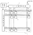
図1は、電気光学装置のブロック構成図である。表示部1には、mドット×nライン分の画素2がマトリクス状(二次元平面的)に並んでいるとともに、水平方向に延在している水平ライン群Y1〜Ynと、垂直方向に延在しているデータ線群X1〜Xmとが配置されている。1つの水平ラインY(YはY1〜Ynの任意の1つを指す)は、2本の走査線と1本の信号線で構成されており、それぞれに対して、第1の走査信号SEL1、第2の走査信号SEL2、パルス信号PLSが出力される。これらの走査信号SEL1,SEL2は、基本的に、互いに排他的な論理レベルをとるが、一方の変化タイミングを若干ずらすこともある。それぞれの画素2は、水平ライン群Y1〜Ynとデータ線群X1〜Xmとの各交差に対応して配置されている。パルス信号PLSは、ある画素2が選択されてから、この画素2が次に選択されるまでの期間(本実施形態では1垂直走査期間)において、その画素2を構成する電気光学素子をインパルス駆動させる制御信号である。なお、本実施形態では、1つの画素2を画像の最小表示単位としているが、1つの画素2を複数のサブ画素で構成してもよい。また、図1では、各画素2に所定の固定電位Vdd,Vssを供給する電源線等が省略されている。
【0031】
制御回路5は、図示しない上位装置より入力される垂直同期信号Vs、水平同期信号Hs、ドットクロック信号DCLKおよび階調データD等に基づいて、走査線駆動回路3とデータ線駆動回路4とを同期制御する。この同期制御の下、走査線駆動回路3およびデータ線駆動回路4は、互いに協働して、表示部1の表示制御を行う。
【0032】
走査線駆動回路3は、シフトレジスタ、出力回路等を主体に構成されており、走査線に走査信号SEL1,SEL2を出力することによって、走査線を順番に選択していく。このような線順次走査により、1垂直走査期間において、所定の走査方向に(一般的には最上から最下に向かって)、1水平ライン分の画素群に相当する画素行が順番に選択されていく。
【0033】
一方、データ線駆動回路4は、シフトレジスタ、ラインラッチ回路、出力回路等を主体に構成されている。本実施形態において、データ線駆動回路4は、電流プログラム方式を用いる関係上、画素2の表示階調に相当するデータ(データ電圧Vdata)をデータ電流Idataへと変換する可変電流源を含む。データ線駆動回路4は、1水平走査期間において、今回データを書き込む画素行に対するデータ電流Idataの一斉出力と、次の水平走査期間で書き込みを行う画素行に関するデータの点順次的なラッチとを同時に行う。ある水平走査期間において、データ線Xの本数に相当するm個のデータが順次ラッチされる。そして、次の水平走査期間において、ラッチされたm個のデータは、データ電流Idataに変換された上で、それぞれのデータ線X1〜Xmに対して一斉に出力される。なお、データ線駆動回路4に対してフレームメモリ等(図示せず)から直接データを線順次的に入力する構成でも本発明を適用できるが、その場合においても本発明の主眼とする部分の動作は同様であるので説明を省略する。この場合、データ線駆動回路4にシフトレジスタを含む必要がなくなる。
【0034】
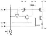
図2は、本実施形態に係る画素2の回路図である。1つの画素2は、有機EL素子OLED、能動素子である5つのトランジスタT1〜T5、および、データを保持するキャパシタCによって構成されている。ダイオードとして表記された有機EL素子OLEDは、自己に供給された駆動電流Ioledによって発光輝度が制御される電流駆動型の素子である。なお、この画素回路では、nチャネル型のトランジスタT1,T5と、pチャネル型のトランジスタT2〜T4とが用いられているが、これは一例であって、本発明はこれに限定されるものではない。
【0035】
第1のスイッチングトランジスタT1のゲートは、第1の走査信号SEL1が供給される走査線に接続され、そのソースは、データ電流Idataが供給されるデータ線X(XはX1〜Xmの任意の1本を指す)に接続されている。また、第1のスイッチングトランジスタT1のドレインは、第2のスイッチングトランジスタT2のドレインと、プログラミングトランジスタT3のドレインとに共通接続されている。第2の走査信号SEL2がゲートに供給された第2のスイッチングトランジスタT2のソースは、カレントミラー回路を構成する一対のトランジスタT3,T4のゲートと、キャパシタCの一方の電極とに共通接続されている。プログラミングトランジスタT3のソース、駆動素子の一形態である駆動トランジスタT4のソースおよびキャパシタCの他方の電極には、電源電位Vddが印加されている。制御素子の一形態であって、パルス信号PLSがゲートに供給された制御トランジスタT5は、駆動電流Ioledの電流経路中、具体的には、駆動トランジスタT4のドレインと有機EL素子OLEDのアノード(陽極)との間に設けられている。この有機EL素子OLEDのカソード(陰極)には、電源電位Vddより低い電位Vssが印加されている。プログラミングトランジスタT3および駆動トランジスタT4は、両者のゲートが互いに接続されたカレントミラー回路を構成している。したがって、プログラミングトランジスタT3のチャネルを流れるデータ電流Idataの電流レベルと、駆動トランジスタT4のチャネルを流れる駆動電流Ioledの電流レベルとは、比例関係になる。
【0036】
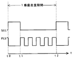
図3は、本実施形態に係る画素2の駆動タイミングチャートである。走査線駆動回路3の線順次走査によって、ある画素2の選択が開始されるタイミングをt0とし、その画素2の選択が次に開始されるタイミングをt2とする。この1垂直走査期間t0〜t2は、前半のプログラミング期間t0〜t1と、後半の駆動期間t1〜t2とに分けられる。
【0037】
まず、プログラミング期間t0〜t1では、画素2の選択によって、キャパシタCに対するデータの書き込みが行われる。タイミングt0において、第1の走査信号SEL1が高レベル(以下、「Hレベル」という)に立ち上がり、第1のスイッチングトランジスタT1がオンする。これにより、データ線XとプログラミングトランジスタT3のドレインとが電気的に接続される。この第1の走査信号SEL1の立ち上がりと同期して、第2の走査信号SEL2が低レベル(以下、「Lレベル」という)に立ち下がって、第2のスイッチングトランジスタT2もオンする。これにより、プログラミングトランジスタT3は、自己のゲートが自己のドレインに接続されたダイオード接続となり、非線形な抵抗素子として機能する。したがって、プログラミングトランジスタT3は、データ線Xより供給されたデータ電流Idataを自己のチャネルに流し、データ電流Idataに応じたゲート電圧Vgを自己のゲートに発生させる。プログラミングトランジスタT3のゲートに接続されたキャパシタCには、発生したゲート電圧Vgに応じた電荷が蓄積され、データが書き込まれる。
【0038】
プログラミング期間t0〜t1では、パルス信号PLSがLレベルに維持されているため、制御トランジスタT5はオフのままである。したがって、カレントミラー回路を構成する一対のトランジスタT3,T4の閾値の関係に拘わらず、有機EL素子OLEDに対する電流経路が遮断され続ける。そのため、この期間t0〜t1において、有機EL素子OLEDは発光しない。
【0039】
つぎに、駆動期間t1〜t2では、キャパシタCの蓄積電荷に応じた駆動電流Ioledが有機EL素子OLEDを流れ、有機EL素子OLEDが発光する。まず、タイミングt1において、第1の走査信号SEL1がLレベルに立ち下がり、第1のスイッチングトランジスタT1がオフする。これにより、データ線XとプログラミングトランジスタT3のドレインとが電気的に分離され、プログラミングトランジスタT3に対するデータ電流Idataの供給が停止する。この第1の走査信号SEL1の立ち下がりと同期して、第2の走査信号SEL2がHレベルに立ち上がって、第2のスイッチングトランジスタT2もオフする。これにより、プログラミングトランジスタT3のゲートとドレインとの間が電気的に分離される。駆動トランジスタT4のゲートには、キャパシタCに蓄積された電荷によって、ゲート電圧Vg相当が印加される。
【0040】
タイミングt1における第1の走査信号SEL1の立ち下がりと同期して、それ以前はLレベルだったパルス信号PLSは、HレベルとLレベルとが交互に繰り返されるパルス状の波形へと変化する。このパルス波形は、画素2の次の選択が開始されるタイミングt2に至るまで継続される。これにより、パルス信号PLSによって導通制御される制御トランジスタT5は、オンとオフとを交互に繰り返すことになる。制御トランジスタT5がオンの場合、電源電位Vddから電位Vssに向かって、駆動トランジスタT4と制御トランジスタT5と有機EL素子OLEDとを介した電流経路が形成される。有機EL素子OLEDを流れる駆動電流Ioledは、その電流値を設定する駆動トランジスタT4のチャネル電流に相当し、キャパシタCの蓄積電荷に起因したゲート電圧Vgによって制御される。有機EL素子OLEDは、駆動電流Ioledに応じた輝度で発光する。上述したカレントミラー構成により、有機EL素子OLEDの発光輝度を規定する駆動電流Ioled(駆動トランジスタT4のチャネル電流)は、データ線Xより供給されたデータ電流Idata(プログラミングトランジスタT3のチャネル電流)に比例する。一方、制御トランジスタT5がオフの場合、駆動電流Ioledの電流経路が制御トランジスタT5によって強制的に遮断される。したがって、制御トランジスタT5のオフ期間では、有機EL素子OLEDの発光が一時的に停止し、黒表示となる。このように、駆動期間t1〜t2では、駆動電流Ioledの電流経路中に設けられた制御トランジスタT5のオンとオフとが複数回行われるため、有機EL素子OLEDの発光と非発光とが複数回繰り返される。
【0041】
このように、本実施形態では、制御トランジスタT5の導通制御により、画素2が選択されてから次に選択されるまでの期間t0〜t2において、駆動電流Ioledの電流経路の遮断が繰り返される。このため、駆動期間t1〜t2において、有機EL素子OLEDの発光と非発光とが複数回行われる。その結果、画素2の光学応答をインパルス型に近づけることができる。また、この期間t1〜t2において、有機EL素子OLEDが非発光となる期間(黒表示の期間)が分散されるため、表示画像のちらつきの低減を図ることができる。その結果、表示品質の一層の向上を図ることができる。それとともに、画素2の光学応答を改善することにより、動画表示等における疑似輪郭の発生も有効に抑制可能となる。
【0042】
また、本実施形態によれば、駆動電流Ioledの電流経路中に制御トランジスタT5を設けることにより、カレントミラー回路を構成する一対のトランジスタT3,T4の閾値の制約を解消できる。上述した特許文献1に開示されたカレントミラー回路を有する画素回路では、駆動電流Ioledの電流経路中に、制御トランジスタT5が設けられていない。そのため、駆動トランジスタT4の閾値は、プログラミングトランジスタT3の閾値よりも低くならないように設定する必要がある。なぜなら、この関係を具備しない場合、キャパシタCに対するデータの書き込みが十分に完了しないうちに、駆動トランジスタT4がオンしてしまい、これに起因したリーク電流によって、有機EL素子OLEDが発光してしまうからである。さらに、駆動トランジスタT4を完全にオフすることができずに有機EL素子OLEDを完全に消灯できない、つまり「黒」表示ができないという問題が発生する場合がある。これに対して、本実施形態のように、駆動電流Ioledの電流経路中に制御トランジスタT5を追加し、プログラミング期間t0〜t1中、これをオフさせておけば、トランジスタT3,T4の閾値の関係に依存することなく、駆動電流Ioledの電流経路を強制的に遮断できる。その結果、プログラミング期間t0〜t1において、駆動トランジスタT4のリーク電流に起因した有機EL素子OLEDの発光を確実に防止でき、表示品質の一層の向上を図ることができる。
【0043】
なお、上述した実施形態では、駆動期間t1〜t2において、パルス信号PLSの波形をパルス状にした例について説明した。しかしながら、上述したリーク電流に起因した有機EL素子OLEDの発光防止のみに着目するならば、少なくともプログラミング期間t0〜t1において、制御トランジスタT5がオフしていれば足りる。したがって、例えば、図4に示すように、プログラミング期間t0〜t1ではパルス信号PLSをLレベルに維持し、これに続く駆動期間t1〜t2ではパルス信号PLSをHレベルに維持してもよい。また、第2のスイッチングトランジスタT2をnチャネル型に変更してT2のゲートに走査信号SEL1を接続する構成でも同様の効果が得られる。その場合は走査線SEL1が不要となるので画素を構成する回路規模が小さくなり、歩留まり向上や開口率向上に貢献できる。
【0044】
(第2の実施形態)
本実施形態は、駆動トランジスタがプログラミングトランジスタとしての機能も担う、電流プログラム方式における画素回路の構成に関する。なお、後述する各実施形態を含めて、電気光学装置の全体構成は、基本的には、1つの水平ラインYの構成を除いて、図1と同様である。本実施形態において、1つの水平ラインYは、走査信号SELが供給される1本の走査線と、パルス信号PLSが供給される1本の信号線とによって構成されている。
【0045】
図5は、本実施形態に係る画素2の回路図である。1つの画素2は、有機EL素子OLED、4つのトランジスタT1,T2,T4,T5およびキャパシタCによって構成されている。なお、本実施形態に係る画素回路において、トランジスタT1,T2,T4,T5のタイプはすべてpチャネル型であるが、これは一例であって、本発明はこれに限定されるものではない。
【0046】
第1のスイッチングトランジスタT1のゲートは、走査信号SELが供給される走査線に接続され、そのソースは、データ電流Idataが供給されるデータ線Xに接続されている。第1のスイッチングトランジスタT1のドレインは、制御トランジスタT5のドレインと、駆動トランジスタT4のソースと、キャパシタCの一方の電極とに共通接続されている。キャパシタCの他方の電極は、駆動トランジスタT4のゲートと、第2のスイッチングトランジスタT2のソースとに共通接続されている。第2のスイッチングトランジスタT2のゲートは、第1のスイッチングトランジスタT1と同様に、走査信号SELが供給される走査線に接続されている。第2のスイッチングトランジスタT2のドレインは、駆動トランジスタT4のドレインと、有機EL素子OLEDのアノードとに共通接続されている。この有機EL素子OLEDのカソードには、電位Vssが印加されている。制御トランジスタT5のゲートは、パルス信号PLSが供給される信号線に接続され、そのソースには、電源電位Vddが印加されている。
【0047】
図6は、本実施形態に係る画素2の駆動タイミングチャートである。図5の画素回路では、1垂直走査期間t0〜t2のほぼ全体に亘って、有機EL素子OLEDに電流が流れるため、有機EL素子OLEDが発光する。上述した実施形態と同様に、1垂直走査期間t0〜t2は、プログラミング期間t0〜t1と駆動期間t1〜t2とに分けられる。
【0048】
まず、プログラミング期間t0〜t1では、画素2の選択によって、キャパシタCに対するデータの書き込みが行われる。タイミングt0において、走査信号SELがLレベルに立ち下がり、スイッチングトランジスタT1,T2が共にオンする。これにより、データ線Xと駆動トランジスタT4のソースとが電気的に接続されるとともに、駆動トランジスタT4は、自己のゲートと自己のドレインとが電気的に接続されたダイオード接続となる。これにより、駆動トランジスタT4は、データ線Xより供給されたデータ電流Idataを自己のチャネルに流し、このデータ電流Idataに応じたゲート電圧Vgを自己のゲートに発生させる。駆動トランジスタT4のゲートとソースとの間に接続されたキャパシタCには、発生したゲート電圧Vgに応じた電荷が蓄積され、データが書き込まれる。このように、プログラミング期間t0〜t1において、駆動トランジスタT4は、キャパシタCにデータを書き込むプログラミングトランジスタとして機能する。
【0049】
プログラミング期間t0〜t1では、パルス信号PLSがHレベルに維持されているため、制御トランジスタT5はオフのままである。したがって、電源電位Vddから電位Vssに向かう駆動電流Ioledの電流経路自体は遮断され続ける。しかしながら、データ線Xと電位Vssとの間に、第1のスイッチングトランジスタT1と駆動トランジスタT4と有機EL素子OLEDとを介した、データ電流Idataの電流経路が形成される。したがって、プログラミング期間t0〜t1においても、データ電流Idataに応じた輝度で有機EL素子OLEDが発光する。
【0050】
つぎに、駆動期間t1〜t2では、キャパシタCに蓄積された電荷に応じた駆動電流Ioledが有機EL素子OLEDを流れ、有機EL素子OLEDが発光する。まず、駆動開始タイミングt1において、走査信号SELがHレベルに立ち上がり、スイッチングトランジスタT1,T2が共にオフする。これにより、データ電流Idataが供給されたデータ線Xと駆動トランジスタT4のソースとが電気的に分離され、駆動トランジスタT4のゲートとドレインとの間も電気的に分離される。駆動トランジスタT4のゲートには、キャパシタCの蓄積電荷に応じて、ゲート電圧Vg相当が印加される。
【0051】
タイミングt1における走査信号SELの立ち上がりと同期して、それ以前はHレベルだったパルス信号PLSは、パルス波形へと変化する。これにより、パルス信号PLSによって導通制御される制御トランジスタT5は、オンとオフとを交互に繰り返すことになる。制御トランジスタT5がオンの場合、駆動電流Ioledの電流経路が形成される。有機EL素子OLEDを流れる駆動電流Ioledは、キャパシタCの蓄積電荷に起因したゲート電圧Vgによって制御され、この電流レベルに応じた輝度で、有機EL素子OLEDが発光する。一方、制御トランジスタT5がオフの場合、駆動電流Ioledの電流経路が制御トランジスタT5によって強制的に遮断される。このような制御トランジスタT5の導通制御を通じて、駆動期間t1〜t2において、有機EL素子OLEDの発光が断続的に繰り返される。
【0052】
本実施形態によれば、制御トランジスタT5の導通制御により、画素2が選択されてから次に選択されるまでの期間t0〜t2において、駆動電流Ioledの電流経路の遮断が複数回行われる。このため、駆動期間t1〜t2において、有機EL素子OLEDの発光と非発光とが繰り返される。その結果、第1の実施形態と同様に、画素2の光学応答をインパルス型に近づけることができ、かつ、黒表示を分散させることによって、表示画像のちらつきの低減を図ることができる。その結果、表示品質の一層の向上を図ることが可能となる。
【0053】
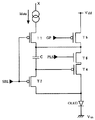
なお、本実施形態では、有機EL素子OLEDの断続的な発光を、駆動電流Ioledの電流経路中に存在する制御トランジスタT5の導通制御により行っている。しかしながら、例えば、図7または図8に示すように、駆動電流Ioledの電流経路中に、制御トランジスタT5とは別に第2の制御トランジスタT6を追加した場合でも、同様のことを実現できる。図7の画素回路では、第2の制御トランジスタT6を、第1の制御トランジスタT5のドレインと駆動トランジスタT4のソースとの間に設けている。また、図8の画素回路では、第2の制御トランジスタT6を、駆動トランジスタT4のドレインと有機EL素子OLEDのアノードとの間に設けている。第2の制御トランジスタT6は、一例として、nチャネル型のトランジスタであり、そのゲートには、パルス信号PLSが供給される。一方、第1の制御トランジスタT5のゲートには、制御信号GPが供給される。
【0054】
図9は、図7または図8の画素2の駆動のタイミングチャートである。制御信号GPは、プログラミング期間t0〜t1において、Hレベルに維持される。したがって、駆動電流Ioledの電流経路は、制御信号GPで導通制御される制御トランジスタT5によって複数回遮断される。また、このプログラミング期間t0〜t1では、パルス信号PLSがHレベルになるため、第2の制御トランジスタT6がオンする。したがって、図5の画素回路と同様に、データ電流Idataの電流経路が形成されて、キャパシタCにデータが書き込まれるとともに、有機EL素子OLEDが発光する。続く駆動期間t1〜t2では、制御信号GPがHレベルになるとともに、パルス信号PLSがパルス波形になる。したがって、パルス信号PLSによる第2の制御トランジスタT6の導通制御を通じて、有機EL素子OLEDの発光が断続的に繰り返される。
【0055】
(第3の実施形態)
本実施形態は、駆動トランジスタがプログラミングトランジスタとしての機能も担う、電流プログラム方式における画素回路の構成に関する。本実施形態において、1つの水平ラインYは、走査信号SELが供給される1本の走査線と、パルス信号PLSが供給される1本の信号線とによって構成されている。
【0056】
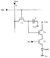
図10は、本実施形態に係る画素2の回路図である。1つの画素2は、有機EL素子OLED、4つのトランジスタT1,T2,T4,T5およびキャパシタCによって構成されている。なお、本実施形態に係る画素回路では、nチャネル型のトランジスタT1,T2,T5とpチャネル型のトランジスタT4とが用いられているが、これは一例であって、本発明はこれに限定されるものではない。
【0057】
第1のスイッチングトランジスタT1のゲートは、走査信号SELが供給される走査線に接続され、そのソースは、データ電流Idataが供給されるデータ線Xに接続されている。第1のスイッチングトランジスタT1のドレインは、第2のスイッチングトランジスタT2のソースと、駆動トランジスタT4のドレインと、制御トランジスタT5のドレインとに共通接続されている。第2のスイッチングトランジスタT2のゲートは、第1のスイッチングトランジスタT1と同様に、走査信号SELが供給される走査線に接続されている。第2のスイッチングトランジスタT2のドレインは、キャパシタCの一方の電極と、駆動トランジスタT4のゲートとに共通接続されている。キャパシタCの他方の電極と駆動トランジスタT4のソースとには、電源電位Vddが印加されている。パルス信号PLSがゲートに供給された制御トランジスタT5は、駆動トランジスタT4のドレインと有機EL素子OLEDのアノードとの間に設けられている。この有機EL素子OLEDのカソードには、電位Vssが印加されている。
【0058】
図11は、本実施形態に係る画素2の駆動タイミングチャートである。上述した実施形態と同様、1垂直走査期間t0〜t2は、プログラミング期間t0〜t1と駆動期間t1〜t2とに分けられる。
【0059】
まず、プログラミング期間t0〜t1では、画素2の選択によって、キャパシタCに対するデータの書き込みが行われる。タイミングt0において、走査信号SELがHレベルに立ち上がり、スイッチングトランジスタT1,T2が共にオンする。これにより、データ線Xと駆動トランジスタT4のドレインとが電気的に接続されるとともに、駆動トランジスタT4は、自己のゲートと自己のドレインとが電気的に接続されたダイオード接続となる。これにより、駆動トランジスタT4は、データ線Xより供給されたデータ電流Idataを自己のチャネルに流し、このデータ電流Idataに応じたゲート電圧Vgを自己のゲートに発生させる。駆動トランジスタT4のゲートに接続されたキャパシタCには、発生したゲート電圧Vgに応じた電荷が蓄積され、データが書き込まれる。このように、プログラミング期間t0〜t1において、駆動トランジスタT4は、キャパシタCにデータを書き込むプログラミングトランジスタとして機能する。
【0060】
プログラミング期間t0〜t1では、パルス信号PLSがLレベルに維持されているため、制御トランジスタT5はオフのままである。したがって、有機EL素子OLEDに対する駆動電流Ioledの電流経路が遮断され続けるため、この期間t0〜t1において、有機EL素子OLEDは発光しない。
【0061】
つぎに、駆動期間t1〜t2では、キャパシタCに蓄積された電荷に応じた駆動電流Ioledが有機EL素子OLEDを流れ、有機EL素子OLEDが発光する。まず、駆動開始タイミングt1において、走査信号SELがLレベルに立ち下がり、スイッチングトランジスタT1,T2が共にオフする。これにより、データ電流Idataが供給されたデータ線Xと駆動トランジスタT4のドレインとが電気的に分離され、駆動トランジスタT4のゲートとドレインとの間も電気的に分離される。駆動トランジスタT4のゲートには、キャパシタCの蓄積電荷に応じて、ゲート電圧Vg相当が印加される。
【0062】
タイミングt1における走査信号SELの立ち下がりと同期して、それ以前はLレベルだったパルス信号PLSは、パルス波形へと変化する。このパルス波形は、画素2の次の選択が開始されるタイミングt2に至るまで継続される。これにより、パルス信号PLSによって導通制御される制御トランジスタT5は、オンとオフとを交互に繰り返すことになる。制御トランジスタT5がオンの場合、駆動電流Ioledの電流経路が形成されるため、有機EL素子OLEDは、駆動電流Ioledに応じた輝度で発光する。一方、制御トランジスタT5がオフの場合、駆動電流Ioledの電流経路が制御トランジスタT5によって強制的に遮断される。このような制御トランジスタT5の導通制御を通じて、駆動電流Ioledの電流経路の遮断が繰り返されるため、有機EL素子OLEDの発光と非発光とが複数回行われる。
【0063】
このように、本実施形態によれば、上述した実施形態と同様に、画素2の光学応答をインパルス型に近づけることができ、かつ、黒表示を分散させることによって、表示画像のちらつきの低減を図ることができる。その結果、表示品質の一層の向上を図ることができる。
【0064】
(第4の実施形態)
本実施形態は、電圧プログラム方式における画素回路の構成に係り、特に、CC(Conductance Control)法と呼ばれるものに関する。ここで、「電圧プログラム方式」とは、データ線Xに対するデータの供給を電圧ベースで行う方式をいう。本実施形態において、1つの水平ラインYは、走査信号SELが供給される1本の走査線と、パルス信号PLSが供給される1本の信号線とによって構成されている。電圧プログラム方式では、データ電圧Vdataをデータ線Xにそのまま出力する関係上、データ線駆動回路4に可変電流源を設ける必要はない。
【0065】
図12は、本実施形態に係る画素2の回路図である。1つの画素2は、有機EL素子OLED、3つのトランジスタT1,T4,T5およびキャパシタCによって構成されている。なお、本実施形態に係る画素回路では、トランジスタT1,T4,T5のタイプはすべてnチャネル型であるが、これは一例であって、本発明はこれに限定されるものではない。
【0066】
スイッチングトランジスタT1のゲートは、走査信号SELが供給される走査線に接続され、そのドレインは、データ電圧Vdataが供給されるデータ線Xに接続されている。スイッチングトランジスタT1のソースは、キャパシタCの一方の電極と、駆動トランジスタT4のゲートとに共通接続されている。キャパシタCの他方の電極には電位Vssが印加されており、駆動トランジスタT4のドレインには電源電位Vddが印加されている。制御トランジスタT5は、パルス信号PLSによって導通制御され、そのソースは、有機EL素子OLEDのアノードに接続されている。この有機EL素子OLEDのカソードには、電位Vssが印加されている。
【0067】
図13は、本実施形態に係る画素2の駆動タイミングチャートである。まず、タイミングt0において、走査線SELがHレベルに立ち上がり、スイッチングトランジスタT1がオンする。これにより、データ線Xに供給されたデータ電圧Vdataが、スイッチングトランジスタT1を介して、キャパシタCの一方の電極に印加され、データ電圧Vdata相当の電荷がキャパシタCに蓄積される(データの書き込み)。なお、タイミングt0からタイミングt1までの期間において、パルス信号PLSはLレベルに維持されるため、制御トランジスタT5はオフのままである。したがって、有機EL素子OLEDに対する駆動電流Ioledの電流経路が遮断されるため、前半の期間t0〜t1において、有機EL素子OLEDは発光しない。
【0068】
前半の期間t0〜t1に続く後半の期間t1〜t2では、キャパシタCに蓄積された電荷に応じた駆動電流Ioledが有機EL素子OLEDを流れ、有機EL素子OLEDが発光する。タイミングt1では、走査信号SELがLレベルに立ち下がり、スイッチングトランジスタT1がオフする。これにより、キャパシタCの一方の電極に対するデータ電圧Vdataの印加が停止するが、キャパシタCの蓄積電荷によって、駆動トランジスタT4のゲートにはゲート電圧Vg相当が印加される。
【0069】
タイミングt1における走査信号SELの立ち下がりと同期して、それ以前はLレベルだったパルス信号PLSは、パルス波形へと変化する。このパルス波形は、画素2の次の選択が開始されるタイミングt2に至るまで継続される。このような制御トランジスタT5の導通制御を通じて、駆動電流Ioledの電流経路の遮断が複数回行われるため、有機EL素子OLEDの発光と非発光とが繰り返される。
【0070】
このように、本実施形態によれば、上述した実施形態と同様に、画素2の光学応答をインパルス型に近づけることができ、かつ、黒表示を分散させることによって、表示画像のちらつきの低減を図ることができる。その結果、表示品質の一層の向上を図ることができる。なお、本実施形態において、パルス信号PLSの波形をパルス状にする開始タイミングは、走査信号SELの立ち下がりタイミングt1と同じでもよいが、特に低階調データの書き込みの安定性を考慮するならば、これよりも所定の時間だけ早く設定してもよい。
【0071】
(第5の実施形態)
本実施形態は、電圧プログラム方式の画素回路を駆動する画素回路の構成に関する。本実施形態において、1つの水平ラインYは、第1の走査信号および第2の走査信号がそれぞれ供給される2本の走査線と、パルス信号PLSが供給される1本の信号線とによって構成されている。
【0072】
図14は、本実施形態に係る画素2の回路図である。1つの画素2は、有機EL素子OLED、4つのトランジスタT1,T2,T4,T5および2つのキャパシタC1,C2によって構成されている。なお、本実施形態に係る画素回路では、トランジスタT1,T2,T4,T5のタイプがすべてpチャネル型であるが、これは一例であって、本発明はこれに限定されるものではない。
【0073】
第1のスイッチングトランジスタT1のゲートは、走査信号SELが供給される走査線が接続され、そのソースは、データ電圧Vdataが供給されるデータ線Xに接続されている。第1のスイッチングトランジスタT1のドレインは、第1のキャパシタC1の一方の電極に接続されている。また、第1のキャパシタC1の他方の電極は、第2のキャパシタC2の一方の電極と、第2のスイッチングトランジスタT2のソースと、駆動トランジスタT4のゲートとに共通接続されている。第2のキャパシタC2の他方の電極と駆動トランジスタT4のソースとには、電源電位Vddが印加されている。第2のスイッチングトランジスタT2のゲートには第2の走査信号SEL2が供給され、そのドレインは、駆動トランジスタT4のドレインと制御トランジスタT5のソースとに共通接続されている。パルス信号PLSがゲートに供給された制御トランジスタT5は、駆動トランジスタT4のドレインと有機EL素子OLEDのアノードとの間に設けられている。この有機EL素子OLEDのカソードには、電位Vssが印加されている。
【0074】
図15は、本実施形態に係る画素2の駆動タイミングチャートである。1垂直走査期間t0〜t4は、期間t0〜t1と、オートゼロ期間t1〜t2と、ロードデータ期間t2〜t3と、駆動期間t3〜t4とに分けられる。
【0075】
まず、期間t0〜t1において、駆動トランジスタT4のドレインの電位が電位Vssに設定される。具体的には、タイミングt0において、第1および第2の走査信号SEL1,SEL2が共にLレベルに立ち下がって、第1および第2のスイッチングトランジスタT1,T2が共にオンする。この期間t0〜t1では、データ線Xに対して電源電位Vddが固定的に印加されているため、第1のキャパシタC1の一方の電極には電源電位Vddが印加される。また、この期間t0〜t1では、パルス信号PLSがLレベルに維持されているため、制御トランジスタT5がオンする。これにより、制御トランジスタT5と有機EL素子OLEDとを介した電流経路が形成され、駆動トランジスタT4のドレイン電位が電位Vssとなる。したがって、駆動トランジスタT4のソースを基準としたゲート電圧Vgsがマイナスになって、駆動トランジスタT4がオンする。
【0076】
つぎに、オートゼロ期間t1〜t2において、駆動トランジスタT4のゲート電圧Vgsが閾値電圧Vthになる。この期間t1〜t2では、走査信号SEL1,SEL2は共にLレベルなので、スイッチングトランジスタT1,T2のオン状態が維持される。タイミングt1において、パルス信号PLSがHレベルに立ち上がり、制御トランジスタT5がオフになるが、第1のキャパシタC1の一方の電極には、データ線からの電源電位Vddの印加が継続される。駆動トランジスタT4のゲートには、自己のチャネルと第2のスイッチングトランジスタT2とを介して、自己のソースに印加された電源電位Vddが印加される。これにより、駆動トランジスタT4のゲート間電圧Vgsは、自己の閾値電圧Vthまで押し上げられ、ゲート電圧Vgsが閾値電圧Vthになった時点で、駆動トランジスタT4がオフになる。その結果、駆動トランジスタT4のゲートに接続された2つのキャパシタC1,C2の電極には、それぞれ閾値電圧Vthが印加されることになる。一方、キャパシタC1,C2の対向する電極には、データ線Xからの電源電位Vddが印加されているので、それぞれのキャパシタC1,C2の電位差は、電源電位Vddと閾値電圧Vthとの差(Vdd−Vth)に設定される(オートゼロ)。
【0077】
続くロードデータ期間t2〜t3において、オートゼロに設定されたキャパシタC1,C2に対するデータの書き込みが行われる。この期間t2〜t3において、第1の走査信号SEL1は、それ以前と同様にLレベルに維持され、パルス信号PLSも、それ以前と同様にHレベルに維持されている。したがって、第1のスイッチングトランジスタT1はオンしたままであり、制御トランジスタT5はオフしたままである。しかしながら、タイミングt2において、第2の走査信号SEL2がHレベルに立ち上がるため、第2のスイッチングトランジスタT2がオンからオフに変化する。また、データ電圧Vdataとして、従前の電源電位VddからΔVdataだけ低下させた電圧レベルがデータ線Xに印加される。変化量ΔVdataは、画素2に書き込むデータに応じた可変値であり、これにより、第1のキャパシタC1の電位差が低下する。このように第1のキャパシタC1の電位差を変化させると、キャパシタC1,C2の容量分割の関係に従い、第2のキャパシタC2の電位差も変化する。変化後の各キャパシタC1,C2の電位差は、オートゼロ期間t1〜t2での電位差(Vdd−Vth)から変化量ΔVdata相当を差し引いた値によって決まる。変化量ΔVdataに起因したキャパシタC1,C2の電位差の変化によって、それぞれのキャパシタC1,C2に対してデータが書き込まれる。
【0078】
最後に、駆動期間t3〜t4において、第2のキャパシタC2に蓄積された電荷に応じた駆動電流Ioledが有機EL素子OLEDを流れ、有機EL素子OLEDが発光する。タイミングt3において、第1の走査信号SEL1がHレベルに立ち上がり、第1のスイッチングトランジスタT1がオンからオフに変化する(第2のスイッチングトランジスタT2はオフのままである)。また、データ線Xの電圧は、電源電位Vddへと復帰する。これにより、データ電源電位Vddが印加されたデータ線Xと第1のキャパシタC1の一方の電極とが分離されるとともに、駆動トランジスタT4のゲートとドレインとの間も分離される。したがって、駆動トランジスタT4のゲートには、第2のキャパシタC2の蓄積電荷に応じた電圧(ソースを基準としたゲート電圧Vgs)が印加される。なお、駆動トランジスタT4を流れる電流Ids(駆動電流Ioledに相当)の算出式には、駆動トランジスタT4の閾値電圧Vthとゲート電圧Vgsとが変数として含まれる。しかしながら、ゲート電圧Vgsとして、第2のキャパシタC2の電位差(Vgsに相当)を代入した場合、駆動電流Ioledの算出式において、閾値電圧Vthが相殺される。その結果、駆動電流Ioledは、駆動トランジスタT4の閾値電圧Vthの影響を受けることなく、データ電圧の変化量ΔVdataのみに依存することになる。
【0079】
駆動電流Ioledの電流経路は、電源電位Vddから電位Vssに向かって、駆動トランジスタT4と制御トランジスタT5と有機EL素子OLEDとを介した経路となる。この駆動電流Ioledは、駆動トランジスタT4のチャネル電流に相当し、第2のキャパシタC2の蓄積電荷に起因したゲート電圧Vgsによって制御される。駆動期間t3〜t4では、上述した各実施形態と同様に、パルス信号PLSがパルス状になるため、この信号PLSによって導通制御される制御トランジスタT5は、オンとオフとを交互に繰り返す。その結果、駆動電流Ioledの電流経路の遮断が繰り返されるため、有機EL素子OLEDの発光と非発光とが交互に行われる。
【0080】
このように、本実施形態において、制御トランジスタT5は、駆動期間t3〜t4において、駆動電流Ioledの電流経路の遮断を繰り返し、この駆動期間t3〜t4を除く期間t0〜t3において、駆動電流Ioledの電流経路を遮断し続ける。これにより、上述した実施形態と同様に、画素2の光学応答をインパルス型に近づけることができ、かつ、黒表示を分散させることによって、表示画像のちらつきの低減を図ることができる。その結果、表示品質の一層の向上を図ることができる。なお、本実施形態では、タイミングt4において、パルス信号PLSのパルス波形を終了しているが、特に低階調データの書き込みの安定性を考慮するならば、タイミングt4よりも所定の時間だけ早く終了させてもよい。
【0081】
なお、上述した各実施形態では、電気光学素子として有機EL素子OLEDを用いた例について説明した。しかしながら、本発明はこれに限定されるものではなく、それ以外の、駆動電流に応じた輝度で発光する電気光学素子に対して適用可能である。
【0082】
また、上述した各実施形態に係る電気光学装置は、例えば、プロジェクタ、携帯電話機、携帯端末、モバイル型コンピュータ、パーソナルコンピュータ等を含む様々な電子機器に実装可能である。これらの電子機器に上述した電気光学装置を実装すれば、電子機器の商品価値を一層高めることができ、市場における電子機器の商品訴求力の向上を図ることができる。
【0083】
【発明の効果】
このように、本発明によれば、駆動電流に応じた輝度で発光する電気光学素子を有する画素において、駆動電流の電流経路を遮断する、制御素子の一形態である制御トランジスタを設ける。そして、ある画素に対応する走査線が選択されてから、この走査線が次に選択されるまでの期間において、制御トランジスタの導通制御によって、駆動電流の電流経路を適宜のタイミングで遮断する。これにより、表示品質の一層の向上を図ることができる。
【図面の簡単な説明】
【図1】第1の実施形態に係る電気光学装置のブロック構成図。
【図2】第1の実施形態に係る画素の回路図。
【図3】第1の実施形態に係る画素の駆動タイミングチャート。
【図4】第1の実施形態に係る画素の他の駆動タイミングチャート。
【図5】第2の実施形態に係る画素の回路図。
【図6】第2の実施形態に係る画素の駆動タイミングチャート。
【図7】第2の実施形態に係る画素の回路図の変形例。
【図8】第2の実施形態に係る画素の回路図の他の変形例。
【図9】第2の実施形態に係る画素の駆動タイミングチャート。
【図10】第3の実施形態に係る画素の回路図。
【図11】第3の実施形態に係る画素の駆動タイミングチャート。
【図12】第4の実施形態に係る画素の回路図。
【図13】第4の実施形態に係る画素の駆動タイミングチャート。
【図14】第5の実施形態に係る画素の回路図。
【図15】第5の実施形態に係る画素の駆動タイミングチャート。
【符号の説明】
1 表示部
2 画素
3 走査線駆動回路
4 データ線駆動回路
5 制御回路
T1 第1のスイッチングトランジスタ
T2 第2のスイッチングトランジスタ
T3 プログラミングトランジスタ
T4 駆動トランジスタ
T5 制御トランジスタ
T6 第2の制御トランジスタ
C キャパシタ
C1 第1のキャパシタ
C2 第2のキャパシタ
OLED 有機EL素子[0001]
TECHNICAL FIELD OF THE INVENTION
The present invention relates to an electro-optical device using an electro-optical element whose emission luminance is controlled by a current, a driving method of the electro-optical device, and an electronic apparatus, and more particularly to a technique for interrupting a current path of a driving current.
[0002]
[Prior art]
In recent years, a flat panel display (FPD) using an organic EL (Electronic Luminescence) element has attracted attention. The organic EL element is a typical current-driven element driven by a current flowing through the element, and emits light at a luminance corresponding to the current level. Driving methods of an active matrix display using an organic EL element are roughly classified into a voltage programming method and a current programming method.
[0003]
For example,
[0004]
Further, for example,
[0005]
[Patent Document 1]
JP 2001-6076 A
[Patent Document 2]
JP 2001-147659 A
[Patent Document 3]
JP-T-2002-514320.
[0006]
[Problems to be solved by the invention]
An object of the present invention is to improve display quality in an electro-optical device using an electro-optical element that emits light at a luminance corresponding to a drive current.
[0007]
[Means for Solving the Problems]
In order to solve such a problem, a first aspect of the present invention provides a plurality of scanning lines, a plurality of data lines, a plurality of pixels arranged corresponding to intersections of the scanning lines and the data lines, and a plurality of scanning lines. By outputting a signal, a scan line driver circuit for selecting a scan line corresponding to a pixel to which data is to be written, and a data line corresponding to a pixel to be written in cooperation with the scan line driver circuit. Provided is an electro-optical device having a data line driving circuit for outputting data. Here, each of the pixels includes an electro-optical element that emits light at a luminance corresponding to the driving current, a capacitor for writing data by accumulating a charge corresponding to data supplied through the data line, It has a driving transistor and a control transistor. The drive transistor sets a drive current in accordance with the charge stored in the capacitor, and supplies the set drive current to the electro-optical element. The control transistor repeatedly cuts off the current path of the drive current during a period from the time when the scanning line corresponding to the pixel to be written is selected to the time when this scanning line is next selected.
[0008]
Here, the first invention may be applied to a current programming method. When the current programming method is applied, the data line driving circuit outputs data as a data current to the data line. Each of the pixels further has a programming transistor. The programming transistor generates a gate voltage when a data current flows through its own channel. Electric charges corresponding to the generated gate voltage are accumulated in the capacitor, whereby data is written to the capacitor.
[0009]
Further, the first invention may be applied to a voltage programming method. When applied to the voltage programming method, the data line driving circuit outputs data as a data voltage to the data line. Writing data to the capacitor is performed based on the data voltage.
[0010]
In the first invention, it is preferable that the conduction of the control transistor be controlled by a pulse signal output from the scanning line driving circuit. In this case, the scanning line driving circuit generates a pulse signal supplied to the pixel to be written in synchronism with the scanning signal supplied to the pixel to be written, by a pulse in which a high level and a low level are alternately repeated. It is preferable to make the shape.
[0011]
A second invention is to output a first scanning signal to a plurality of scanning lines, a plurality of data lines, a plurality of pixels arranged corresponding to intersections of the scanning lines and the data lines, and a scanning line. Selects a scan line corresponding to a pixel to which data is to be written, and outputs a second scan signal synchronized with the first scan signal and a pulse signal synchronized with the first scan signal. An electro-optical device includes a line driving circuit and a data line driving circuit that outputs a data current to a data line corresponding to a pixel to be written in cooperation with a scanning line driving circuit. Here, each of the pixels includes five transistors, a capacitor, and an electro-optical element. The first switching transistor has one of a source and a drain connected to the data line, and is controlled by a first scan signal. One of a source and a drain of the second switching transistor is connected to the other terminal of the first switching transistor, and is controlled by a second scan signal. The capacitor is connected to the other terminal of the second switching transistor. The programming transistor has a drain commonly connected to the other terminal of the first switching transistor and one terminal of the second switching transistor, and a gate commonly connected to the other terminal of the second switching transistor and a capacitor. That is, the charge corresponding to the data current is accumulated in a capacitor connected to its own gate. The drive transistor forms a current mirror circuit in combination with the programming transistor, and sets a drive current in accordance with the charge stored in the capacitor connected to the gate. The electro-optical element emits light at a luminance according to the drive current. The control transistor is provided in the current path of the drive current, and interrupts the current path of the drive current by controlling the conduction of the pulse signal.
[0012]
Here, in the second invention, the control transistor is connected to the current path of the drive current during a period from when a scanning line corresponding to a pixel to be written is selected to when the scanning line is next selected. Preferably, the blocking is repeated. In this case, the control transistor cuts off the current path of the drive current during the programming period during the period from the time when the scanning line corresponding to the pixel to be written is selected to the time when this scanning line is next selected. It is desirable that the current path of the drive current be repeatedly interrupted in the drive period following the programming period.
[0013]
Further, in the second invention, from the viewpoint of preventing leakage current of the drive transistor, the control transistor selects a scan line corresponding to a pixel to be written, and then selects this scan line next. During the programming period, the current path of the driving current may be interrupted during the programming period, and the current path of the driving current may not be interrupted during the driving period following the programming period.
[0014]
According to a third aspect of the present invention, a plurality of scanning lines, a plurality of data lines, a plurality of pixels arranged corresponding to intersections of the scanning lines and the data lines, and a scanning signal are output to the scanning lines. A scanning line driving circuit that outputs a pulse signal synchronized with the scanning signal while selecting a scanning line corresponding to the pixel to be written, and cooperates with the scanning line driving circuit to correspond to the pixel to be written. And a data line driving circuit for outputting a data current to the data line. Here, each of the pixels has four transistors, a capacitor, and an electro-optical element. The first switching transistor has one of a source and a drain connected to the data line, and is controlled by a scan signal. The second switching transistor is controlled by the scan signal. The capacitor is connected between the other terminal of the first switching transistor and one terminal of the second switching transistor. The driving transistor has a source connected to the other terminal of the first switching transistor, a gate connected to one terminal of the second switching transistor, and a drain connected to the other terminal of the second switching transistor. . The drive transistor stores a charge corresponding to the data current in a capacitor connected between its own gate and its own source, and sets a drive current in accordance with the charge stored in the capacitor. The electro-optical element emits light at a luminance according to the drive current. The control transistor interrupts the current path of the driving current by controlling the conduction of the pulse signal during a period from the time when the scanning line corresponding to the pixel to be written is selected to the time when this scanning line is next selected. repeat.
[0015]
Here, in the third invention, the control transistor is driven during a programming period during a period from a time when a scanning line corresponding to a pixel to be written is selected to a time when this scanning line is next selected. It is preferable that the current path of the current is continuously interrupted and the current path of the drive current is repeatedly interrupted in a driving period following the programming period.
[0016]
According to a fourth aspect of the present invention, a plurality of scan lines, a plurality of data lines, a plurality of pixels arranged corresponding to intersections of the scan lines and the data lines, and a scan signal are output to the scan lines, thereby providing data. A scanning line driving circuit that outputs a pulse signal synchronized with the scanning signal while selecting a scanning line corresponding to the pixel to be written, and cooperates with the scanning line driving circuit to correspond to the pixel to be written. And a data line driving circuit for outputting a data current to the data line. Here, each of the pixels has four transistors, a capacitor, and an electro-optical element. The first switching transistor has one of a source and a drain connected to the data line, and is controlled by a scan signal. One of a source and a drain of the second switching transistor is connected to the other terminal of the first switching transistor, and is controlled by a scan signal. The capacitor is connected to the other terminal of the second switching transistor. The drive transistor has a gate commonly connected to the other terminal of the second switching transistor and the capacitor, and a drain commonly connected to the other terminal of the first switching transistor and one terminal of the second switching transistor. I have. The drive transistor stores a charge corresponding to the data current in a capacitor connected to its own gate, and sets a drive current according to the charge stored in the capacitor. The electro-optical element emits light at a luminance according to the drive current. The control transistor interrupts the current path of the driving current by controlling the conduction of the pulse signal during a period from the time when the scanning line corresponding to the pixel to be written is selected to the time when this scanning line is next selected. repeat.
[0017]
Here, in the fourth invention, the control transistor is driven during a programming period during a period from a time when a scanning line corresponding to a pixel to be written is selected to a time when the next scanning line is selected. It is preferable that the current path of the current is continuously interrupted and the current path of the drive current is repeatedly interrupted in a driving period following the programming period.
[0018]
According to a fifth aspect of the present invention, a plurality of scan lines, a plurality of data lines, a plurality of pixels arranged corresponding to intersections of the scan lines and the data lines, and a scan signal are output to the scan lines, thereby providing data. A scanning line driving circuit that outputs a pulse signal synchronized with the scanning signal while selecting a scanning line corresponding to the pixel to be written, and cooperates with the scanning line driving circuit to correspond to the pixel to be written. And a data line driving circuit for outputting a data voltage to the data line. Here, each of the pixels has three transistors, a capacitor, and an electro-optical element. The switching transistor has one of a source and a drain connected to the data line, and is controlled by a scan signal. The capacitor is connected to the other terminal of the switching transistor, and stores a charge according to the data voltage. The drive transistor has a gate commonly connected to the other terminal of the switching transistor and the capacitor, and sets a drive current according to the electric charge stored in the capacitor. The electro-optical element emits light at a luminance according to the drive current. The control transistor interrupts the current path of the driving current by controlling the conduction of the pulse signal during a period from the time when the scanning line corresponding to the pixel to be written is selected to the time when this scanning line is next selected. repeat.
[0019]
Here, in the fifth invention, the control transistor is configured such that in the first half of a period from when a scanning line corresponding to a pixel to be written is selected to when this scanning line is selected next, It is preferable that the current path of the driving current is continuously interrupted, and the interruption of the current path of the driving current is repeated in a second half period following the first half period.
[0020]
A sixth invention is to output a first scanning signal to a plurality of scanning lines, a plurality of data lines, a plurality of pixels arranged corresponding to intersections of the scanning lines and the data lines, and a scanning line. Selects a scan line corresponding to a pixel to which data is to be written, and outputs a second scan signal synchronized with the first scan signal and a pulse signal synchronized with the first scan signal. An electro-optical device includes a line driving circuit and a data line driving circuit that outputs a data voltage to a data line corresponding to a pixel to be written in cooperation with a scanning line driving circuit. Here, each of the pixels has four transistors, two capacitors, and an electro-optical element. The first switching transistor has one of a source and a drain connected to the data line, and is controlled by a first scan signal. The first capacitor has one electrode connected to the other terminal of the first switching transistor, and the second capacitor has a power supply potential applied to one electrode. The second switching transistor has one terminal of a source or a drain commonly connected to the other electrode of the first capacitor and the other electrode of the second capacitor, and is controlled by a second scanning signal. The driving transistor has a gate commonly connected to one terminal of the second switching transistor, the other terminal of the first capacitor, and the other terminal of the second capacitor, and has one electrode of the second capacitor connected to the source. And the other terminal of the second switching transistor is connected to the drain. The drive transistor stores a charge corresponding to the data current in the second capacitor, and sets a drive current in accordance with the charge stored in the second capacitor. The electro-optical element emits light at a luminance according to the drive current. The control transistor interrupts the current path of the driving current by controlling the conduction of the pulse signal during a period from the time when the scanning line corresponding to the pixel to be written is selected to the time when this scanning line is next selected. repeat.
[0021]
Here, in the sixth invention, the control transistor is configured to drive during a driving period in a period from a time when a scanning line corresponding to a pixel to be written is selected to a time when this scanning line is next selected. It is preferable that the current path of the current is repeatedly interrupted and the current path of the drive current is continuously interrupted during a period excluding the driving period.
[0022]
According to a seventh aspect, there is provided an electronic apparatus on which the electro-optical device according to any one of the first to sixth aspects is mounted.
[0023]
According to an eighth aspect, a plurality of pixels arranged corresponding to intersections of a scanning line and a data line and a scanning line corresponding to a pixel to which data is to be written are output by outputting a scanning signal to the scanning line. And a data line driving circuit that cooperates with the scanning line driving circuit and outputs data to a data line corresponding to a pixel to be written. . This driving method includes a first step of outputting data to a data line corresponding to a pixel to be written, and a method according to data supplied to a capacitor of the pixel to be written via a data line. A second step of accumulating the electric charge, and a driving current corresponding to the electric charge stored in the capacitor is set by the driving transistor of the pixel to be written, and the set driving current is changed to a luminance corresponding to the driving current. In the third step of supplying the electro-optical element which emits light in the period, and in the period from the time when the scanning line corresponding to the pixel to be written is selected to the time when this scanning line is next selected, And a fourth step of repeating the blocking of the path.
[0024]
Here, in the eighth invention, the first step is a step of outputting data as a data current to the data line, and in the second step, the data current supplied to the data line is converted into a voltage. Then, data may be written to the capacitor according to the converted voltage.
[0025]
Also, in the eighth invention, the first step is a step of outputting data as a data voltage to the data line, and the second step is a step of outputting a capacitor according to the data voltage supplied to the data line. May be written.
[0026]
Further, in the fourth step of the eighth invention, it is preferable that the interruption of the current path of the drive current is repeated in synchronization with the scanning signal supplied to the pixel to be written.
[0027]
The ninth invention outputs a plurality of scanning lines, a plurality of data lines, a plurality of pixels arranged corresponding to intersections of the scanning lines and the plurality of data lines, and outputting a scanning signal to the scanning lines. A scanning line driving circuit for selecting a scanning line corresponding to a pixel to which data is to be written, and a data line for cooperating with the scanning line driving circuit and outputting data to a data line corresponding to the pixel to be written An electro-optical device having a driving circuit is provided. Here, each of the pixels includes an electro-optical element that emits light at a luminance corresponding to the drive current, a holding unit that holds data supplied via the data line, and an electric device that emits light in accordance with the data held by the holding unit. A drive element for setting a drive current to be supplied to the optical element, and a current path of the drive current during a period from when a scanning line corresponding to a pixel to be written is selected to when this scanning line is next selected. And a control element that repeats the cutoff.
[0028]
According to a tenth aspect, a plurality of pixels arranged corresponding to intersections of a scanning line and a data line and a scanning line corresponding to a pixel to which data is to be written by outputting a scanning signal to the scanning line. And a data line driving circuit that cooperates with the scanning line driving circuit and outputs data to a data line corresponding to a pixel to be written. . This driving method includes a first step of outputting data to a data line corresponding to a pixel to be written, and a step of holding data supplied via the data line to holding means of the pixel to be written. By doing so, a second step of writing data, and a driving element corresponding to the data held in the holding unit is set by a driving element of a pixel to be written, and the set driving current is set to: A third step of supplying a current-driven electro-optical element that emits light at a luminance corresponding to the drive current, and a scan line corresponding to a pixel to be written is selected, and then this scan line is selected next A fourth step of repeatedly interrupting the current path of the drive current during the period until
[0029]
BEST MODE FOR CARRYING OUT THE INVENTION
(1st Embodiment)
The present embodiment relates to an electro-optical device using a current programming method, and particularly to display control of an active matrix display in which each pixel includes a current mirror circuit. Here, the “current programming method” refers to a method of supplying data to the data lines on a current basis.
[0030]
FIG. 1 is a block diagram of the electro-optical device. In the
[0031]
The
[0032]
The scanning
[0033]
On the other hand, the data
[0034]
FIG. 2 is a circuit diagram of the
[0035]
The gate of the first switching transistor T1 is connected to a scanning line to which a first scanning signal SEL1 is supplied, and its source is connected to a data line X (X is any one of X1 to Xm) to which a data current Idata is supplied. Connected to the book). The drain of the first switching transistor T1 is commonly connected to the drain of the second switching transistor T2 and the drain of the programming transistor T3. The source of the second switching transistor T2 whose gate is supplied with the second scanning signal SEL2 is commonly connected to the gates of a pair of transistors T3 and T4 forming a current mirror circuit and one electrode of the capacitor C. I have. A power supply potential Vdd is applied to the source of the programming transistor T3, the source of the drive transistor T4 which is a form of the drive element, and the other electrode of the capacitor C. The control transistor T5, which is an embodiment of the control element and has the pulse signal PLS supplied to its gate, is connected to the drain of the drive transistor T4 and the anode (anode) of the organic EL element OLED in the current path of the drive current Ioled. ). A potential Vss lower than the power supply potential Vdd is applied to a cathode (cathode) of the organic EL element OLED. The programming transistor T3 and the driving transistor T4 form a current mirror circuit in which both gates are connected to each other. Therefore, the current level of the data current Idata flowing through the channel of the programming transistor T3 is proportional to the current level of the driving current Ioled flowing through the channel of the driving transistor T4.
[0036]
FIG. 3 is a driving timing chart of the
[0037]
First, in the programming period t0 to t1, data is written to the capacitor C by selecting the
[0038]
In the programming period t0 to t1, the pulse signal PLS is maintained at the L level, so that the control transistor T5 remains off. Therefore, the current path to the organic EL element OLED continues to be interrupted irrespective of the relationship between the threshold values of the pair of transistors T3 and T4 constituting the current mirror circuit. Therefore, the organic EL element OLED does not emit light during this period t0 to t1.
[0039]
Next, during the drive period t1 to t2, the drive current Ioled according to the charge stored in the capacitor C flows through the organic EL element OLED, and the organic EL element OLED emits light. First, at timing t1, the first scanning signal SEL1 falls to the L level, and the first switching transistor T1 turns off. As a result, the data line X is electrically separated from the drain of the programming transistor T3, and the supply of the data current Idata to the programming transistor T3 is stopped. In synchronization with the fall of the first scan signal SEL1, the second scan signal SEL2 rises to the H level, and the second switching transistor T2 also turns off. Thus, the gate and the drain of the programming transistor T3 are electrically separated. A gate voltage Vg equivalent is applied to the gate of the driving transistor T4 by the electric charge stored in the capacitor C.
[0040]
In synchronization with the fall of the first scanning signal SEL1 at the timing t1, the pulse signal PLS, which was at the L level before that, changes to a pulse-like waveform in which the H level and the L level are alternately repeated. This pulse waveform is continued until the timing t2 when the next selection of the
[0041]
As described above, in the present embodiment, the current path of the drive current Ioled is repeatedly interrupted in the period from t0 to t2 from the time when the
[0042]
Further, according to the present embodiment, by providing the control transistor T5 in the current path of the drive current Ioled, it is possible to eliminate the restriction on the threshold value of the pair of transistors T3 and T4 forming the current mirror circuit. In the pixel circuit having the current mirror circuit disclosed in
[0043]
In the above-described embodiment, an example has been described in which the waveform of the pulse signal PLS is pulsed in the driving period t1 to t2. However, if attention is paid only to the prevention of light emission of the organic EL element OLED caused by the above-described leakage current, it is sufficient that the control transistor T5 is turned off at least in the programming period t0 to t1. Therefore, for example, as shown in FIG. 4, the pulse signal PLS may be maintained at the L level during the programming period t0 to t1, and the pulse signal PLS may be maintained at the H level during the subsequent driving period t1 to t2. The same effect can be obtained by changing the second switching transistor T2 to an n-channel type and connecting the scanning signal SEL1 to the gate of T2. In that case, since the scanning line SEL1 becomes unnecessary, the circuit scale of the pixel is reduced, which can contribute to improvement in yield and aperture ratio.
[0044]
(Second embodiment)
The present embodiment relates to a configuration of a pixel circuit in a current programming system in which a driving transistor also functions as a programming transistor. The overall configuration of the electro-optical device, including the embodiments described below, is basically the same as that of FIG. 1 except for the configuration of one horizontal line Y. In this embodiment, one horizontal line Y includes one scanning line to which the scanning signal SEL is supplied and one signal line to which the pulse signal PLS is supplied.
[0045]
FIG. 5 is a circuit diagram of the
[0046]
The gate of the first switching transistor T1 is connected to the scanning line to which the scanning signal SEL is supplied, and the source is connected to the data line X to which the data current Idata is supplied. The drain of the first switching transistor T1 is commonly connected to the drain of the control transistor T5, the source of the drive transistor T4, and one electrode of the capacitor C. The other electrode of the capacitor C is commonly connected to the gate of the driving transistor T4 and the source of the second switching transistor T2. The gate of the second switching transistor T2 is connected to the scanning line to which the scanning signal SEL is supplied, similarly to the first switching transistor T1. The drain of the second switching transistor T2 is commonly connected to the drain of the driving transistor T4 and the anode of the organic EL element OLED. The potential Vss is applied to the cathode of the organic EL element OLED. The gate of the control transistor T5 is connected to a signal line to which the pulse signal PLS is supplied, and the power supply potential Vdd is applied to its source.
[0047]
FIG. 6 is a driving timing chart of the
[0048]
First, in the programming period t0 to t1, data is written to the capacitor C by selecting the
[0049]
During the programming period t0 to t1, the pulse signal PLS is maintained at the H level, so that the control transistor T5 remains off. Therefore, the current path itself of the drive current Ioled from the power supply potential Vdd to the potential Vss continues to be interrupted. However, a current path of the data current Idata is formed between the data line X and the potential Vss via the first switching transistor T1, the driving transistor T4, and the organic EL element OLED. Therefore, even during the programming period t0 to t1, the organic EL element OLED emits light at a luminance corresponding to the data current Idata.
[0050]
Next, during the driving period t1 to t2, the driving current Ioled according to the electric charge stored in the capacitor C flows through the organic EL element OLED, and the organic EL element OLED emits light. First, at the drive start timing t1, the scanning signal SEL rises to the H level, and both the switching transistors T1 and T2 are turned off. As a result, the data line X to which the data current Idata is supplied is electrically separated from the source of the driving transistor T4, and the gate and drain of the driving transistor T4 are also electrically separated. A gate voltage Vg equivalent is applied to the gate of the driving transistor T4 according to the charge stored in the capacitor C.
[0051]
In synchronization with the rise of the scanning signal SEL at the timing t1, the pulse signal PLS which was at the H level before that changes to a pulse waveform. As a result, the control transistor T5, whose conduction is controlled by the pulse signal PLS, alternately turns on and off. When the control transistor T5 is on, a current path for the drive current Ioled is formed. The drive current Ioled flowing through the organic EL element OLED is controlled by the gate voltage Vg caused by the charge stored in the capacitor C, and the organic EL element OLED emits light at a luminance according to the current level. On the other hand, when the control transistor T5 is off, the current path of the drive current Ioled is forcibly cut off by the control transistor T5. Through the conduction control of the control transistor T5, the light emission of the organic EL element OLED is intermittently repeated in the driving period t1 to t2.
[0052]
According to the present embodiment, the current path of the driving current Ioled is cut off a plurality of times during the period from t0 to t2 from the selection of the
[0053]
In the present embodiment, the organic EL element OLED emits light intermittently by controlling the conduction of the control transistor T5 existing in the current path of the drive current Ioled. However, for example, as shown in FIG. 7 or FIG. 8, the same can be realized even when a second control transistor T6 is added separately from the control transistor T5 in the current path of the drive current Ioled. In the pixel circuit of FIG. 7, the second control transistor T6 is provided between the drain of the first control transistor T5 and the source of the drive transistor T4. In the pixel circuit of FIG. 8, the second control transistor T6 is provided between the drain of the driving transistor T4 and the anode of the organic EL element OLED. The second control transistor T6 is, for example, an n-channel transistor, and has a gate supplied with the pulse signal PLS. On the other hand, the control signal GP is supplied to the gate of the first control transistor T5.
[0054]
FIG. 9 is a timing chart of driving the
[0055]
(Third embodiment)
The present embodiment relates to a configuration of a pixel circuit in a current programming system in which a driving transistor also functions as a programming transistor. In this embodiment, one horizontal line Y includes one scanning line to which the scanning signal SEL is supplied and one signal line to which the pulse signal PLS is supplied.
[0056]
FIG. 10 is a circuit diagram of the
[0057]
The gate of the first switching transistor T1 is connected to the scanning line to which the scanning signal SEL is supplied, and the source is connected to the data line X to which the data current Idata is supplied. The drain of the first switching transistor T1 is commonly connected to the source of the second switching transistor T2, the drain of the driving transistor T4, and the drain of the control transistor T5. The gate of the second switching transistor T2 is connected to the scanning line to which the scanning signal SEL is supplied, similarly to the first switching transistor T1. The drain of the second switching transistor T2 is commonly connected to one electrode of the capacitor C and the gate of the driving transistor T4. The power supply potential Vdd is applied to the other electrode of the capacitor C and the source of the driving transistor T4. The control transistor T5 whose pulse signal PLS is supplied to the gate is provided between the drain of the driving transistor T4 and the anode of the organic EL element OLED. The potential Vss is applied to the cathode of the organic EL element OLED.
[0058]
FIG. 11 is a driving timing chart of the
[0059]
First, in the programming period t0 to t1, data is written to the capacitor C by selecting the
[0060]
In the programming period t0 to t1, the pulse signal PLS is maintained at the L level, so that the control transistor T5 remains off. Therefore, since the current path of the drive current Ioled to the organic EL element OLED is continuously interrupted, the organic EL element OLED does not emit light during this period t0 to t1.
[0061]
Next, during the driving period t1 to t2, the driving current Ioled according to the electric charge stored in the capacitor C flows through the organic EL element OLED, and the organic EL element OLED emits light. First, at the drive start timing t1, the scanning signal SEL falls to the L level, and both the switching transistors T1 and T2 are turned off. Thus, the data line X to which the data current Idata is supplied is electrically separated from the drain of the driving transistor T4, and the gate and drain of the driving transistor T4 are also electrically separated. A gate voltage Vg equivalent is applied to the gate of the driving transistor T4 according to the charge stored in the capacitor C.
[0062]
In synchronization with the falling of the scanning signal SEL at the timing t1, the pulse signal PLS which was at the L level before that changes to a pulse waveform. This pulse waveform is continued until the timing t2 when the next selection of the
[0063]
As described above, according to the present embodiment, similarly to the above-described embodiment, the optical response of the
[0064]
(Fourth embodiment)
The present embodiment relates to a configuration of a pixel circuit in a voltage programming system, and particularly to a configuration called a CC (Conductance Control) method. Here, the “voltage programming method” refers to a method of supplying data to the data line X on a voltage basis. In this embodiment, one horizontal line Y includes one scanning line to which the scanning signal SEL is supplied and one signal line to which the pulse signal PLS is supplied. In the voltage programming method, it is not necessary to provide a variable current source in the data
[0065]
FIG. 12 is a circuit diagram of the
[0066]
The gate of the switching transistor T1 is connected to the scanning line to which the scanning signal SEL is supplied, and the drain is connected to the data line X to which the data voltage Vdata is supplied. The source of the switching transistor T1 is commonly connected to one electrode of the capacitor C and the gate of the driving transistor T4. The potential Vss is applied to the other electrode of the capacitor C, and the power supply potential Vdd is applied to the drain of the drive transistor T4. The conduction of the control transistor T5 is controlled by the pulse signal PLS, and its source is connected to the anode of the organic EL element OLED. The potential Vss is applied to the cathode of the organic EL element OLED.
[0067]
FIG. 13 is a driving timing chart of the
[0068]
In the second half period t1 to t2 following the first half period t0 to t1, the drive current Ioled according to the electric charge accumulated in the capacitor C flows through the organic EL element OLED, and the organic EL element OLED emits light. At timing t1, the scanning signal SEL falls to the L level, and the switching transistor T1 turns off. As a result, the application of the data voltage Vdata to one electrode of the capacitor C is stopped. However, the gate charge of the driving transistor T4 is applied to the gate of the driving transistor T4 by the accumulated charge of the capacitor C.
[0069]
In synchronization with the falling of the scanning signal SEL at the timing t1, the pulse signal PLS which was at the L level before that changes to a pulse waveform. This pulse waveform is continued until the timing t2 when the next selection of the
[0070]
As described above, according to the present embodiment, similarly to the above-described embodiment, the optical response of the
[0071]
(Fifth embodiment)
The present embodiment relates to a configuration of a pixel circuit that drives a pixel circuit of a voltage program method. In the present embodiment, one horizontal line Y includes two scanning lines to which the first scanning signal and the second scanning signal are respectively supplied and one signal line to which the pulse signal PLS is supplied. Have been.
[0072]
FIG. 14 is a circuit diagram of the
[0073]
The gate of the first switching transistor T1 is connected to a scanning line to which the scanning signal SEL is supplied, and its source is connected to the data line X to which the data voltage Vdata is supplied. The drain of the first switching transistor T1 is connected to one electrode of the first capacitor C1. The other electrode of the first capacitor C1 is commonly connected to one electrode of the second capacitor C2, the source of the second switching transistor T2, and the gate of the driving transistor T4. The power supply potential Vdd is applied to the other electrode of the second capacitor C2 and the source of the drive transistor T4. A second scanning signal SEL2 is supplied to a gate of the second switching transistor T2, and a drain thereof is commonly connected to a drain of the driving transistor T4 and a source of the control transistor T5. The control transistor T5 whose pulse signal PLS is supplied to the gate is provided between the drain of the driving transistor T4 and the anode of the organic EL element OLED. The potential Vss is applied to the cathode of the organic EL element OLED.
[0074]
FIG. 15 is a driving timing chart of the
[0075]
First, in the period t0 to t1, the potential of the drain of the driving transistor T4 is set to the potential Vss. Specifically, at timing t0, the first and second scanning signals SEL1 and SEL2 both fall to the L level, and both the first and second switching transistors T1 and T2 are turned on. In this period t0 to t1, the power supply potential Vdd is fixedly applied to the data line X, so the power supply potential Vdd is applied to one electrode of the first capacitor C1. In the period t0 to t1, the pulse signal PLS is maintained at the L level, so that the control transistor T5 is turned on. As a result, a current path is formed through the control transistor T5 and the organic EL element OLED, and the drain potential of the drive transistor T4 becomes the potential Vss. Therefore, the gate voltage Vgs based on the source of the driving transistor T4 becomes negative, and the driving transistor T4 is turned on.
[0076]
Next, in the auto-zero period t1 to t2, the gate voltage Vgs of the driving transistor T4 becomes the threshold voltage Vth. During this period t1 to t2, since the scanning signals SEL1 and SEL2 are both at the L level, the on state of the switching transistors T1 and T2 is maintained. At timing t1, the pulse signal PLS rises to the H level and the control transistor T5 is turned off, but the application of the power supply potential Vdd from the data line to one electrode of the first capacitor C1 is continued. The power supply potential Vdd applied to its own source is applied to the gate of the driving transistor T4 via its own channel and the second switching transistor T2. As a result, the gate-to-gate voltage Vgs of the drive transistor T4 is pushed up to its own threshold voltage Vth, and when the gate voltage Vgs reaches the threshold voltage Vth, the drive transistor T4 is turned off. As a result, the threshold voltage Vth is applied to the electrodes of the two capacitors C1 and C2 connected to the gate of the driving transistor T4. On the other hand, since the power supply potential Vdd from the data line X is applied to the opposing electrodes of the capacitors C1 and C2, the potential difference between the capacitors C1 and C2 is the difference between the power supply potential Vdd and the threshold voltage Vth (Vdd −Vth) (auto zero).
[0077]
In the subsequent load data period t2 to t3, data is written to the capacitors C1 and C2 set to auto-zero. During this period t2 to t3, the first scanning signal SEL1 is maintained at the L level as before, and the pulse signal PLS is also maintained at the H level as before. Therefore, the first switching transistor T1 remains on and the control transistor T5 remains off. However, at the timing t2, since the second scanning signal SEL2 rises to the H level, the second switching transistor T2 changes from on to off. As the data voltage Vdata, a voltage level lower than the previous power supply potential Vdd by ΔVdata is applied to the data line X. The change amount ΔVdata is a variable value according to the data to be written to the
[0078]
Finally, in the driving period t3 to t4, the driving current Ioled according to the electric charge stored in the second capacitor C2 flows through the organic EL element OLED, and the organic EL element OLED emits light. At timing t3, the first scanning signal SEL1 rises to the H level, and the first switching transistor T1 changes from on to off (the second switching transistor T2 remains off). Further, the voltage of the data line X returns to the power supply potential Vdd. As a result, the data line X to which the data power supply potential Vdd is applied is separated from one electrode of the first capacitor C1, and the gate and drain of the driving transistor T4 are also separated. Therefore, a voltage (gate voltage Vgs based on the source) according to the accumulated charge of the second capacitor C2 is applied to the gate of the driving transistor T4. The calculation formula of the current Ids (corresponding to the drive current Ioled) flowing through the drive transistor T4 includes the threshold voltage Vth and the gate voltage Vgs of the drive transistor T4 as variables. However, when the potential difference (corresponding to Vgs) of the second capacitor C2 is substituted for the gate voltage Vgs, the threshold voltage Vth is canceled in the calculation formula of the drive current Ioled. As a result, the drive current Ioled depends on only the data voltage change amount ΔVdata without being affected by the threshold voltage Vth of the drive transistor T4.
[0079]
The current path of the drive current Ioled is from the power supply potential Vdd to the potential Vss via the drive transistor T4, the control transistor T5, and the organic EL element OLED. The drive current Ioled corresponds to the channel current of the drive transistor T4, and is controlled by the gate voltage Vgs caused by the charge stored in the second capacitor C2. In the driving period t3 to t4, the pulse signal PLS becomes pulse-shaped, as in the above-described embodiments, and the control transistor T5, which is controlled to be conductive by this signal PLS, alternately turns on and off. As a result, the interruption of the current path of the drive current Ioled is repeated, so that the organic EL element OLED emits light and emits light alternately.
[0080]
As described above, in the present embodiment, the control transistor T5 repeatedly cuts off the current path of the drive current Ioled in the drive periods t3 to t4, and in the period t0 to t3 excluding the drive periods t3 to t4, Continue to interrupt the current path. Thus, as in the above-described embodiment, the optical response of the
[0081]
In each of the embodiments described above, an example in which the organic EL element OLED is used as the electro-optical element has been described. However, the present invention is not limited to this, and can be applied to other electro-optical elements that emit light at a luminance corresponding to the drive current.
[0082]
Further, the electro-optical device according to each of the embodiments described above can be mounted on various electronic devices including, for example, a projector, a mobile phone, a mobile terminal, a mobile computer, a personal computer, and the like. If the above-described electro-optical device is mounted on these electronic devices, the commercial value of the electronic devices can be further increased, and the product appeal of the electronic devices in the market can be improved.
[0083]
【The invention's effect】
As described above, according to the present invention, in a pixel including an electro-optical element that emits light at a luminance corresponding to a drive current, a control transistor that is a form of a control element that blocks a current path of the drive current is provided. Then, during a period from the time when a scanning line corresponding to a certain pixel is selected to the time when the next scanning line is selected, the current path of the driving current is cut off at an appropriate timing by controlling the conduction of the control transistor. Thereby, the display quality can be further improved.
[Brief description of the drawings]
FIG. 1 is a block diagram of an electro-optical device according to a first embodiment.
FIG. 2 is a circuit diagram of a pixel according to the first embodiment.
FIG. 3 is a driving timing chart of the pixel according to the first embodiment.
FIG. 4 is another driving timing chart of the pixel according to the first embodiment.
FIG. 5 is a circuit diagram of a pixel according to a second embodiment.
FIG. 6 is a driving timing chart of a pixel according to a second embodiment.
FIG. 7 is a modified example of a circuit diagram of a pixel according to the second embodiment.
FIG. 8 is another modified example of the circuit diagram of the pixel according to the second embodiment.
FIG. 9 is a driving timing chart of a pixel according to the second embodiment.
FIG. 10 is a circuit diagram of a pixel according to a third embodiment.
FIG. 11 is a drive timing chart of a pixel according to a third embodiment.
FIG. 12 is a circuit diagram of a pixel according to a fourth embodiment.
FIG. 13 is a driving timing chart of a pixel according to a fourth embodiment.
FIG. 14 is a circuit diagram of a pixel according to a fifth embodiment.
FIG. 15 is a driving timing chart of a pixel according to a fifth embodiment.
[Explanation of symbols]
1 Display
2 pixels
3 Scan line drive circuit
4 Data line drive circuit
5 Control circuit
T1 First switching transistor
T2 Second switching transistor
T3 programming transistor
T4 drive transistor
T5 control transistor
T6 Second control transistor
C capacitor
C1 First capacitor
C2 Second capacitor
OLED Organic EL device
Claims (23)
複数の走査線と、
複数のデータ線と、
前記走査線と前記複数のデータ線との交差に対応して配置された複数の画素と、
前記走査線に走査信号を出力することにより、データの書込対象となる画素に対応する前記走査線を選択する走査線駆動回路と、
前記走査線駆動回路と協働し、前記書込対象となる画素に対応する前記データ線にデータを出力するデータ線駆動回路とを有し、
前記画素のそれぞれは、
駆動電流に応じた輝度で発光する電気光学素子と、
前記データ線を介して供給されたデータを保持する保持手段と、
前記保持手段で保持されたデータに応じて、前記電気光学素子に供給する駆動電流を設定する駆動素子と、
前記書込対象となる画素に対応する前記走査線の選択されてから、当該走査線が次に選択されるまでの期間において、前記駆動電流の電流経路の遮断を繰り返す制御素子と
を有することを特徴とする電気光学装置。In electro-optical devices,
Multiple scan lines,
Multiple data lines,
A plurality of pixels arranged corresponding to intersections of the scanning lines and the plurality of data lines,
A scanning line driving circuit that selects a scanning line corresponding to a pixel to be written with data by outputting a scanning signal to the scanning line;
A data line driving circuit that outputs data to the data line corresponding to the pixel to be written in cooperation with the scanning line driving circuit;
Each of the pixels
An electro-optical element that emits light at a luminance according to the drive current;
Holding means for holding data supplied via the data line,
A driving element for setting a driving current to be supplied to the electro-optical element according to the data held by the holding unit;
A control element that repeats interruption of a current path of the drive current during a period from when the scanning line corresponding to the pixel to be written is selected until the next scanning line is selected. Electro-optical device characterized by the following.
複数の走査線と、
複数のデータ線と、
前記走査線と前記データ線との交差に対応して配置された複数の画素と、
前記走査線に走査信号を出力することにより、データの書込対象となる画素に対応する前記走査線を選択する走査線駆動回路と、
前記走査線駆動回路と協働し、前記書込対象となる画素に対応する前記データ線にデータを出力するデータ線駆動回路とを有し、
前記画素のそれぞれは、
駆動電流に応じた輝度で発光する電気光学素子と、
前記データ線を介して供給されたデータに応じた電荷を蓄積することにより、データの書き込みが行われるキャパシタと、
前記キャパシタに蓄積された電荷に応じて、駆動電流を設定し、当該駆動電流を前記電気光学素子に供給する駆動トランジスタと、
前記書込対象となる画素に対応する前記走査線が選択されてから、当該走査線が次に選択されるまでの期間において、前記駆動電流の電流経路の遮断を繰り返す制御トランジスタと
を有することを特徴とする電気光学装置。In electro-optical devices,
Multiple scan lines,
Multiple data lines,
A plurality of pixels arranged corresponding to the intersection of the scanning line and the data line,
A scanning line driving circuit that selects a scanning line corresponding to a pixel to be written with data by outputting a scanning signal to the scanning line;
A data line driving circuit that outputs data to the data line corresponding to the pixel to be written in cooperation with the scanning line driving circuit;
Each of the pixels
An electro-optical element that emits light at a luminance according to the drive current;
A capacitor for writing data by accumulating charges corresponding to the data supplied through the data line;
A drive transistor that sets a drive current according to the charge stored in the capacitor and supplies the drive current to the electro-optical element.
A control transistor that repeats interruption of a current path of the drive current during a period from when the scanning line corresponding to the pixel to be written is selected until the next scanning line is selected. Electro-optical device characterized by the following.
前記画素のそれぞれは、プログラミングトランジスタをさらに有し、
前記プログラミングトランジスタは、自己のチャネルに前記データ電流が流れることにより発生するゲート電圧に基づいて、前記キャパシタに対するデータの書き込みを行うことを特徴とする請求項2に記載された電気光学装置。The data line driving circuit outputs data as a data current to the data line,
Each of the pixels further comprises a programming transistor;
3. The electro-optical device according to claim 2, wherein the programming transistor writes data to the capacitor based on a gate voltage generated when the data current flows through a channel of the programming transistor.
前記キャパシタに対するデータの書き込みは、前記データ電圧に基づいて行われることを特徴とする請求項2に記載された電気光学装置。The data line driving circuit outputs data as a data voltage to the data line,
3. The electro-optical device according to claim 2, wherein writing of data to the capacitor is performed based on the data voltage.
前記走査線駆動回路は、前記書込対象となる画素に供給する前記走査信号と同期して、当該書込対象となる画素に供給する前記パルス信号を、高レベルと低レベルとが交互に繰り返されるパルス状にすることを特徴とする請求項2から4のいずれかに記載された電気光学装置。The conduction control of the control transistor is performed by a pulse signal output from the scanning line driving circuit,
The scanning line drive circuit repeats the pulse signal supplied to the pixel to be written in a high level and a low level alternately in synchronization with the scanning signal supplied to the pixel to be written. 5. The electro-optical device according to claim 2, wherein the electro-optical device has a pulse shape.
複数の走査線と、
複数のデータ線と、
前記走査線と前記データ線との交差に対応して配置された複数の画素と、
前記走査線に第1の走査信号を出力することにより、データの書込対象となる画素に対応する前記走査線を選択するとともに、前記第1の走査信号と同期した第2の走査信号と、前記第1の走査信号と同期したパルス信号とを出力する走査線駆動回路と、
前記走査線駆動回路と協働し、前記書込対象となる画素に対応する前記データ線にデータ電流を出力するデータ線駆動回路とを有し、
前記画素のそれぞれは、
ソースまたはドレインの一方の端子が前記データ線に接続され、前記第1の走査信号によって制御される第1のスイッチングトランジスタと、
ソースまたはドレインの一方の端子が前記第1のスイッチングトランジスタの他方の端子に接続され、前記第2の走査信号によって制御される第2のスイッチングトランジスタと、
前記第2のスイッチングトランジスタの他方の端子に接続されたキャパシタと、
ドレインが前記第1のスイッチングトランジスタの前記他方の端子と前記第2のスイッチングトランジスタの前記一方の端子とに共通接続され、ゲートが前記第2のスイッチングトランジスタの他方の端子と前記キャパシタとに共通接続され、前記データ電流に応じた電荷を自己のゲートに接続された前記キャパシタに蓄積させるプログラミングトランジスタと、
前記プログラミングトランジスタと対になってカレントミラー回路を構成し、ゲートに接続された前記キャパシタに蓄積された電荷に応じて、駆動電流を設定する駆動トランジスタと、
前記駆動電流に応じた輝度で発光する電気光学素子と、
前記駆動電流の電流経路中に設けられ、前記パルス信号の導通制御によって、前記駆動電流の電流経路を遮断する制御トランジスタと
を有することを特徴とする電気光学装置。In electro-optical devices,
Multiple scan lines,
Multiple data lines,
A plurality of pixels arranged corresponding to the intersection of the scanning line and the data line,
Outputting a first scanning signal to the scanning line to select the scanning line corresponding to a pixel to which data is to be written, and a second scanning signal synchronized with the first scanning signal; A scanning line driving circuit that outputs a pulse signal synchronized with the first scanning signal;
A data line driving circuit that outputs a data current to the data line corresponding to the pixel to be written in cooperation with the scanning line driving circuit;
Each of the pixels
A first switching transistor having one terminal of a source or a drain connected to the data line, and controlled by the first scanning signal;
One terminal of a source or a drain is connected to the other terminal of the first switching transistor, and a second switching transistor controlled by the second scanning signal;
A capacitor connected to the other terminal of the second switching transistor;
A drain is commonly connected to the other terminal of the first switching transistor and the one terminal of the second switching transistor, and a gate is commonly connected to the other terminal of the second switching transistor and the capacitor. A programming transistor that stores charge corresponding to the data current in the capacitor connected to its own gate,
A driving transistor that configures a current mirror circuit in combination with the programming transistor, and sets a driving current according to the charge stored in the capacitor connected to the gate;
An electro-optical element that emits light at a luminance according to the drive current;
An electro-optical device, comprising: a control transistor provided in a current path of the drive current, and interrupting the current path of the drive current by controlling conduction of the pulse signal.
複数の走査線と、
複数のデータ線と、
前記走査線と前記データ線との交差に対応して配置された複数の画素と、
前記走査線に走査信号を出力することにより、データの書込対象となる画素に対応する前記走査線を選択するとともに、前記走査信号と同期したパルス信号を出力する走査線駆動回路と、
前記走査線駆動回路と協働し、前記書込対象となる画素に対応する前記データ線にデータ電流を出力するデータ線駆動回路とを有し、
前記画素のそれぞれは、
ソースまたはドレインの一方の端子が前記データ線に接続され、前記走査信号によって制御される第1のスイッチングトランジスタと、
前記走査信号によって制御される第2のスイッチングトランジスタと、
前記第1のスイッチングトランジスタの他方の端子と前記第2のスイッチングトランジスタの一方の端子との間に接続されたキャパシタと、
ソースが前記第1のスイッチングトランジスタの前記他方の端子に接続され、ゲートが前記第2のスイッチングトランジスタの前記一方の端子に接続され、ドレインが前記第2のスイッチングトランジスタの他方の端子に接続され、前記データ電流に応じた電荷を自己のゲートと自己のソースとの間に接続された前記キャパシタに蓄積させるとともに、前記キャパシタに蓄積された電荷に応じて、駆動電流を設定する駆動トランジスタと、
前記駆動電流に応じた輝度で発光する電気光学素子と、
前記書込対象となる画素に対応する前記走査線が選択されてから、当該走査線が次に選択されるまでの期間において、前記パルス信号の導通制御によって、前記駆動電流の電流経路の遮断を繰り返す制御トランジスタと
を有することを特徴とする電気光学装置。In electro-optical devices,
Multiple scan lines,
Multiple data lines,
A plurality of pixels arranged corresponding to the intersection of the scanning line and the data line,
A scanning line driving circuit that outputs a scanning signal to the scanning line, selects the scanning line corresponding to a pixel to which data is to be written, and outputs a pulse signal synchronized with the scanning signal,
A data line driving circuit that outputs a data current to the data line corresponding to the pixel to be written in cooperation with the scanning line driving circuit;
Each of the pixels
A first switching transistor having one terminal of a source or a drain connected to the data line, and controlled by the scan signal;
A second switching transistor controlled by the scanning signal;
A capacitor connected between the other terminal of the first switching transistor and one terminal of the second switching transistor;
A source is connected to the other terminal of the first switching transistor, a gate is connected to the one terminal of the second switching transistor, a drain is connected to the other terminal of the second switching transistor, A drive transistor for storing a charge corresponding to the data current in the capacitor connected between its own gate and its own source, and setting a drive current in accordance with the charge stored in the capacitor,
An electro-optical element that emits light at a luminance according to the drive current;
From the time when the scanning line corresponding to the pixel to be written is selected to the time when the scanning line is selected next, the conduction of the pulse signal is controlled to cut off the current path of the driving current. An electro-optical device, comprising: a control transistor that repeats.
複数の走査線と、
複数のデータ線と、
前記走査線と前記データ線との交差に対応して配置された複数の画素と、
前記走査線に走査信号を出力することにより、データの書込対象となる画素に対応する前記走査線を選択するとともに、前記走査信号と同期したパルス信号を出力する走査線駆動回路と、
前記走査線駆動回路と協働し、前記書込対象となる画素に対応する前記データ線にデータ電流を出力するデータ線駆動回路とを有し、
前記画素のそれぞれは、
ソースまたはドレインの一方の端子が前記データ線に接続され、前記走査信号によって制御される第1のスイッチングトランジスタと、
ソースまたはドレインの一方の端子が前記第1のスイッチングトランジスタの他方の端子に接続され、前記走査信号によって制御される第2のスイッチングトランジスタと、
前記第2のスイッチングトランジスタの他方の端子に接続されたキャパシタと、
ゲートが前記第2のスイッチングトランジスタの前記他方の端子と前記キャパシタとに共通接続され、ドレインが前記第1のスイッチングトランジスタの前記他方の端子と前記第2のスイッチングトランジスタの前記一方の端子とに共通接続され、前記データ電流に応じた電荷を自己のゲートに接続された前記キャパシタに蓄積させるとともに、前記キャパシタに蓄積された電荷に応じて、駆動電流を設定する駆動トランジスタと、
前記駆動電流に応じた輝度で発光する電気光学素子と、
前記書込対象となる画素に対応する前記走査線が選択されてから、当該走査線が次に選択されるまでの期間において、前記パルス信号の導通制御によって、前記駆動電流の電流経路の遮断を繰り返す制御トランジスタと
を有することを特徴とする電気光学装置。In electro-optical devices,
Multiple scan lines,
Multiple data lines,
A plurality of pixels arranged corresponding to the intersection of the scanning line and the data line,
A scanning line driving circuit that outputs a scanning signal to the scanning line, selects the scanning line corresponding to a pixel to which data is to be written, and outputs a pulse signal synchronized with the scanning signal,
A data line driving circuit that outputs a data current to the data line corresponding to the pixel to be written in cooperation with the scanning line driving circuit;
Each of the pixels
A first switching transistor having one terminal of a source or a drain connected to the data line, and controlled by the scan signal;
One terminal of a source or a drain is connected to the other terminal of the first switching transistor, and a second switching transistor controlled by the scan signal;
A capacitor connected to the other terminal of the second switching transistor;
A gate is commonly connected to the other terminal of the second switching transistor and the capacitor, and a drain is common to the other terminal of the first switching transistor and the one terminal of the second switching transistor. A drive transistor that is connected and stores a charge corresponding to the data current in the capacitor connected to its own gate, and sets a drive current according to the charge stored in the capacitor;
An electro-optical element that emits light at a luminance according to the drive current;
From the time when the scanning line corresponding to the pixel to be written is selected to the time when the scanning line is selected next, the conduction of the pulse signal is controlled to cut off the current path of the driving current. An electro-optical device, comprising: a control transistor that repeats.
複数の走査線と、
複数のデータ線と、
前記走査線と前記データ線との交差に対応して配置された複数の画素と、
前記走査線に走査信号を出力することにより、データの書込対象となる画素に対応する前記走査線を選択するとともに、前記走査信号と同期したパルス信号を出力する走査線駆動回路と、
前記走査線駆動回路と協働し、前記書込対象となる画素に対応する前記データ線にデータ電圧を出力するデータ線駆動回路とを有し、
前記画素のそれぞれは、
ソースまたはドレインの一方の端子が前記データ線に接続され、前記走査信号によって制御されるスイッチングトランジスタと、
前記スイッチングトランジスタの他方の端子に接続され、前記データ電圧に応じた電荷を蓄積するキャパシタと、
ゲートが前記スイッチングトランジスタの前記他方の端子と前記キャパシタとに共通接続され、前記キャパシタに蓄積された電荷に応じて、駆動電流を設定する駆動トランジスタと、
前記駆動電流に応じた輝度で発光する電気光学素子と、
前記書込対象となる画素に対応する前記走査線が選択されてから、当該走査線が次に選択されるまでの期間において、前記パルス信号の導通制御によって、前記駆動電流の電流経路の遮断を繰り返す制御トランジスタと
を有することを特徴とする電気光学装置。In electro-optical devices,
Multiple scan lines,
Multiple data lines,
A plurality of pixels arranged corresponding to the intersection of the scanning line and the data line,
A scanning line driving circuit that outputs a scanning signal to the scanning line, selects the scanning line corresponding to a pixel to which data is to be written, and outputs a pulse signal synchronized with the scanning signal,
A data line driving circuit that cooperates with the scanning line driving circuit and outputs a data voltage to the data line corresponding to the pixel to be written;
Each of the pixels
One terminal of a source or a drain is connected to the data line, and a switching transistor controlled by the scan signal;
A capacitor that is connected to the other terminal of the switching transistor and stores a charge corresponding to the data voltage;
A drive transistor having a gate commonly connected to the other terminal of the switching transistor and the capacitor, and setting a drive current according to the charge stored in the capacitor;
An electro-optical element that emits light at a luminance according to the drive current;
From the time when the scanning line corresponding to the pixel to be written is selected to the time when the scanning line is selected next, the conduction of the pulse signal is controlled to cut off the current path of the driving current. An electro-optical device, comprising: a control transistor that repeats.
複数の走査線と、
複数のデータ線と、
前記走査線と前記データ線との交差に対応して配置された複数の画素と、
前記走査線に第1の走査信号を出力することにより、データの書込対象となる画素に対応する前記走査線を選択するとともに、前記第1の走査信号と同期した第2の走査信号と、前記第1の走査信号と同期したパルス信号とを出力する走査線駆動回路と、
前記走査線駆動回路と協働し、前記書込対象となる画素に対応する前記データ線にデータ電圧を出力するデータ線駆動回路とを有し、
前記画素のそれぞれは、
ソースまたはドレインの一方の端子が前記データ線に接続され、前記第1の走査信号によって制御される第1のスイッチングトランジスタと、
一方の電極が前記第1のスイッチングトランジスタの他方の端子に接続された第1のキャパシタと、
一方の電極に電源電位が印加された第2のキャパシタと、
ソースまたはドレインの一方の端子が前記第1のキャパシタの前記他方の電極と前記第2のキャパシタの前記他方の電極とに共通接続され、前記第2の走査信号によって制御される第2のスイッチングトランジスタと、
ゲートが前記第2のスイッチングトランジスタの前記一方の端子と前記第1のキャパシタの前記他方の端子と前記第2のキャパシタの前記他方の端子とに共通接続され、ソースに前記第2のキャパシタの前記一方の電極が接続され、ドレインに前記第2のスイッチングトランジスタの他方の端子が接続され、前記データ電流に応じた電荷を前記第2のキャパシタに蓄積させるとともに、前記第2のキャパシタに蓄積された電荷に応じて、駆動電流を設定する駆動トランジスタと、
前記駆動電流に応じた輝度で発光する電気光学素子と、
前記書込対象となる画素に対応する前記走査線が選択されてから、当該走査線が次に選択されるまでの期間において、前記パルス信号の導通制御によって、前記駆動電流の電流経路の遮断を繰り返す制御トランジスタと
を有することを特徴とする電気光学装置。In electro-optical devices,
Multiple scan lines,
Multiple data lines,
A plurality of pixels arranged corresponding to the intersection of the scanning line and the data line,
Outputting a first scanning signal to the scanning line to select the scanning line corresponding to a pixel to which data is to be written, and a second scanning signal synchronized with the first scanning signal; A scanning line driving circuit that outputs a pulse signal synchronized with the first scanning signal;
A data line driving circuit that cooperates with the scanning line driving circuit and outputs a data voltage to the data line corresponding to the pixel to be written;
Each of the pixels
A first switching transistor having one terminal of a source or a drain connected to the data line, and controlled by the first scanning signal;
A first capacitor having one electrode connected to the other terminal of the first switching transistor;
A second capacitor having a power supply potential applied to one of the electrodes;
A second switching transistor having one terminal of a source or a drain commonly connected to the other electrode of the first capacitor and the other electrode of the second capacitor, and controlled by the second scanning signal; When,
A gate is commonly connected to the one terminal of the second switching transistor, the other terminal of the first capacitor, and the other terminal of the second capacitor, and a source of the second capacitor is connected to the second terminal of the second capacitor. One electrode is connected, the other terminal of the second switching transistor is connected to the drain, and the charge corresponding to the data current is stored in the second capacitor, and the charge is stored in the second capacitor. A drive transistor for setting a drive current according to the charge;
An electro-optical element that emits light at a luminance according to the drive current;
From the time when the scanning line corresponding to the pixel to be written is selected to the time when the scanning line is selected next, the conduction of the pulse signal is controlled to cut off the current path of the driving current. An electro-optical device, comprising: a control transistor that repeats.
前記書込対象となる画素に対応する前記データ線にデータを出力する第1のステップと、
前記書込対象となる前記画素が有する保持手段に、前記データ線を介して供給されたデータを保持することにより、データの書き込みを行う第2のステップと、
前記書込対象となる画素が有する駆動素子によって、前記保持手段に保持されたデータに応じた駆動電流を設定し、当該駆動電流を、駆動電流に応じた輝度で発光する電流駆動型の電気光学素子に供給する第3のステップと、
前記書込対象となる画素に対応する前記走査線が選択されてから、当該走査線が次に選択されるまでの期間において、前記駆動電流の電流経路の遮断を繰り返す第4のステップと
を有することを特徴とする電気光学装置の駆動方法。A plurality of pixels arranged corresponding to intersections of a scanning line and a data line, and a scan for outputting a scanning signal to the scanning line to select the scanning line corresponding to a pixel to which data is to be written A method for driving an electro-optical device, comprising: a line drive circuit; and a data line drive circuit that cooperates with the scan line drive circuit and outputs data to the data line corresponding to the pixel to be written.
A first step of outputting data to the data line corresponding to the pixel to be written;
A second step of writing data by holding data supplied via the data line in a holding unit of the pixel to be written;
A current-driven electro-optical device that sets a drive current according to data held in the holding unit by a drive element included in the pixel to be written, and emits the drive current with luminance according to the drive current. A third step of supplying the element;
And a fourth step of repeatedly interrupting the current path of the drive current during a period from when the scanning line corresponding to the pixel to be written is selected to when the scanning line is next selected. A method for driving an electro-optical device, comprising:
前記書込対象となる画素に対応する前記データ線にデータを出力する第1のステップと、
前記書込対象となる前記画素が有するキャパシタに、前記データ線を介して供給されたデータに応じた電荷を蓄積することにより、データの書き込みを行う第2のステップと、
前記書込対象となる画素が有する駆動トランジスタによって、キャパシタに蓄積された電荷に応じた駆動電流を設定し、当該駆動電流を、駆動電流に応じた輝度で発光する電気光学素子に供給する第3のステップと、
前記書込対象となる画素に対応する前記走査線が選択されてから、当該走査線が次に選択されるまでの期間において、前記駆動電流の電流経路の遮断を繰り返す第4のステップと
を有することを特徴とする電気光学装置の駆動方法。A plurality of pixels arranged corresponding to intersections of a scanning line and a data line, and a scan for outputting a scanning signal to the scanning line to select the scanning line corresponding to a pixel to which data is to be written A method for driving an electro-optical device, comprising: a line drive circuit; and a data line drive circuit that cooperates with the scan line drive circuit and outputs data to the data line corresponding to the pixel to be written.
A first step of outputting data to the data line corresponding to the pixel to be written;
A second step of writing data by accumulating a charge corresponding to the data supplied via the data line in a capacitor of the pixel to be written,
A driving transistor corresponding to the electric charge stored in the capacitor is set by the driving transistor of the pixel to be written, and the driving current is supplied to the electro-optical element that emits light at a luminance corresponding to the driving current. Steps and
And a fourth step of repeatedly interrupting the current path of the drive current during a period from when the scanning line corresponding to the pixel to be written is selected to when the scanning line is next selected. A method for driving an electro-optical device, comprising:
前記第2のステップにおいて、前記データ線に供給された前記データ電流が電圧に変換され、当該変換された電圧に応じて、前記キャパシタに対するデータの書き込みが行われることを特徴とする請求項20に記載された電気光学装置の駆動方法。The first step is a step of outputting data as a data current to the data line,
21. The method according to claim 20, wherein, in the second step, the data current supplied to the data line is converted into a voltage, and data is written to the capacitor according to the converted voltage. A driving method for the described electro-optical device.
前記第2のステップにおいて、前記データ線に供給された前記データ電圧に応じて、前記キャパシタに対するデータの書き込みが行われることを特徴とする請求項20に記載された電気光学装置の駆動方法。The first step is a step of outputting data as a data voltage to the data line,
21. The method according to claim 20, wherein in the second step, data is written to the capacitor in accordance with the data voltage supplied to the data line.
Priority Applications (11)
| Application Number | Priority Date | Filing Date | Title |
|---|---|---|---|
| JP2002360978A JP2004191752A (en) | 2002-12-12 | 2002-12-12 | Electrooptical device, driving method for electrooptical device, and electronic equipment |
| KR1020030080409A KR100594834B1 (en) | 2002-12-12 | 2003-11-14 | Electro-optic apparatus, method of driving the same, and electronic instrument |
| TW092132170A TWI272569B (en) | 2002-12-12 | 2003-11-17 | Electro-optical device, driving method for electro-optical device, and electronic equipment |
| CN2007101622187A CN101127189B (en) | 2002-12-12 | 2003-11-24 | Electro-optical device, method of driving electro-optical device, and electronic apparatus |
| CNB2003101180573A CN100349199C (en) | 2002-12-12 | 2003-11-24 | Electrooptical device, driving method for electrooptical device and electronic equipment |
| US10/724,263 US7259735B2 (en) | 2002-12-12 | 2003-12-01 | Electro-optical device, method of driving electro-optical device, and electronic apparatus |
| EP03257710A EP1429312B1 (en) | 2002-12-12 | 2003-12-08 | Electro-optical device, method of driving electro optical device, and electronic apparatus |
| DE60317761T DE60317761T2 (en) | 2002-12-12 | 2003-12-08 | Electro-optical device, method for driving an electro-optical device and electronic device |
| EP07075846A EP1870875A3 (en) | 2002-12-12 | 2003-12-08 | Electro-optical device, method of driving electro-optical device, and electronic apparatus |
| US11/826,282 US20070257867A1 (en) | 2002-12-12 | 2007-07-13 | Electro-optical device, method of driving electro-optical device, and electronic apparatus |
| US11/826,287 US7999770B2 (en) | 2002-12-12 | 2007-07-13 | Electro-optical device, method of driving electro-optical device, and electronic apparatus |
Applications Claiming Priority (1)
| Application Number | Priority Date | Filing Date | Title |
|---|---|---|---|
| JP2002360978A JP2004191752A (en) | 2002-12-12 | 2002-12-12 | Electrooptical device, driving method for electrooptical device, and electronic equipment |
Related Child Applications (1)
| Application Number | Title | Priority Date | Filing Date |
|---|---|---|---|
| JP2005299754A Division JP4075922B2 (en) | 2005-10-14 | 2005-10-14 | Electro-optical device, driving method of electro-optical device, and electronic apparatus |
Publications (2)
| Publication Number | Publication Date |
|---|---|
| JP2004191752A true JP2004191752A (en) | 2004-07-08 |
| JP2004191752A5 JP2004191752A5 (en) | 2005-08-25 |
Family
ID=32322124
Family Applications (1)
| Application Number | Title | Priority Date | Filing Date |
|---|---|---|---|
| JP2002360978A Pending JP2004191752A (en) | 2002-12-12 | 2002-12-12 | Electrooptical device, driving method for electrooptical device, and electronic equipment |
Country Status (7)
| Country | Link |
|---|---|
| US (3) | US7259735B2 (en) |
| EP (2) | EP1429312B1 (en) |
| JP (1) | JP2004191752A (en) |
| KR (1) | KR100594834B1 (en) |
| CN (2) | CN100349199C (en) |
| DE (1) | DE60317761T2 (en) |
| TW (1) | TWI272569B (en) |
Cited By (16)
| Publication number | Priority date | Publication date | Assignee | Title |
|---|---|---|---|---|
| JPWO2004057561A1 (en) * | 2002-12-19 | 2006-04-27 | 株式会社半導体エネルギー研究所 | Driving method of light emitting device and electronic apparatus |
| JP2006119626A (en) * | 2004-09-24 | 2006-05-11 | Semiconductor Energy Lab Co Ltd | Method of driving light emitting device |
| JP2006259530A (en) * | 2005-03-18 | 2006-09-28 | Seiko Epson Corp | Organic el device, driving method thereof, and electronic device |
| JP2006285117A (en) * | 2005-04-05 | 2006-10-19 | Seiko Epson Corp | Method and circuit for driving electronic circuit, light emission device, and electronic apparatus |
| JP2007316163A (en) * | 2006-05-23 | 2007-12-06 | Sony Corp | Image display device |
| JP2008224853A (en) * | 2007-03-09 | 2008-09-25 | Canon Inc | Display device |
| JP2008304490A (en) * | 2007-06-05 | 2008-12-18 | Sony Corp | Display panel driving method, display device, display panel driving device, and electronic device |
| JP2008304492A (en) * | 2007-06-05 | 2008-12-18 | Sony Corp | Display panel driving method, display device, display panel driving device, and electronic device |
| JP2008304491A (en) * | 2007-06-05 | 2008-12-18 | Sony Corp | Display panel driving method, display device, display panel driving device, and electronic device |
| JP2009025797A (en) * | 2007-06-19 | 2009-02-05 | Canon Inc | Display apparatus and electronic device using the same |
| US8094097B2 (en) | 2004-09-30 | 2012-01-10 | Seiko Epson Corporation | Data line driving circuit, electro-optical device, data line driving method, and electronic apparatus |
| US8674910B2 (en) | 2007-06-05 | 2014-03-18 | Sony Corporation | Display panel driving method, display apparatus, display panel driving apparatus and electronic apparatus |
| US8872868B2 (en) | 2004-09-24 | 2014-10-28 | Semiconductor Energy Laboratory Co., Ltd. | Driving method of light emitting device |
| US10665160B2 (en) | 2016-11-15 | 2020-05-26 | Seiko Epson Corporation | Electrooptical device, electronic apparatus, and driving method of electrooptical device |
| CN112542144A (en) * | 2020-12-02 | 2021-03-23 | Tcl华星光电技术有限公司 | Panel driving circuit and display panel |
| JP2022095867A (en) * | 2006-10-26 | 2022-06-28 | 株式会社半導体エネルギー研究所 | Display device |
Families Citing this family (161)
| Publication number | Priority date | Publication date | Assignee | Title |
|---|---|---|---|---|
| US7569849B2 (en) * | 2001-02-16 | 2009-08-04 | Ignis Innovation Inc. | Pixel driver circuit and pixel circuit having the pixel driver circuit |
| CA2419704A1 (en) | 2003-02-24 | 2004-08-24 | Ignis Innovation Inc. | Method of manufacturing a pixel with organic light-emitting diode |
| CA2443206A1 (en) * | 2003-09-23 | 2005-03-23 | Ignis Innovation Inc. | Amoled display backplanes - pixel driver circuits, array architecture, and external compensation |
| US7196682B2 (en) * | 2003-09-29 | 2007-03-27 | Wintek Corporation | Driving apparatus and method for active matrix organic light emitting display |
| GB0323622D0 (en) * | 2003-10-09 | 2003-11-12 | Koninkl Philips Electronics Nv | Electroluminescent display-devices |
| KR101054327B1 (en) * | 2004-04-30 | 2011-08-04 | 엘지디스플레이 주식회사 | Current driven active matrix organic electroluminescent display device with pixel structure for improving image quality |
| JP4834876B2 (en) * | 2004-06-25 | 2011-12-14 | 京セラ株式会社 | Image display device |
| CA2472671A1 (en) | 2004-06-29 | 2005-12-29 | Ignis Innovation Inc. | Voltage-programming scheme for current-driven amoled displays |
| CN100363967C (en) * | 2004-07-14 | 2008-01-23 | 友达光电股份有限公司 | Pixel driving circuit of active organic light-emitting display |
| KR100592640B1 (en) * | 2004-07-27 | 2006-06-26 | 삼성에스디아이 주식회사 | Light emitting display and scan driver |
| KR100590068B1 (en) * | 2004-07-28 | 2006-06-14 | 삼성에스디아이 주식회사 | Light emitting display, and display panel and pixel circuit thereof |
| KR100846954B1 (en) * | 2004-08-30 | 2008-07-17 | 삼성에스디아이 주식회사 | Light emitting display and driving method thereof |
| WO2006048801A2 (en) * | 2004-11-03 | 2006-05-11 | Koninklijke Philips Electronics N.V. | Electroluminescent display device |
| CA2490858A1 (en) * | 2004-12-07 | 2006-06-07 | Ignis Innovation Inc. | Driving method for compensated voltage-programming of amoled displays |
| US9171500B2 (en) | 2011-05-20 | 2015-10-27 | Ignis Innovation Inc. | System and methods for extraction of parasitic parameters in AMOLED displays |
| WO2006063448A1 (en) | 2004-12-15 | 2006-06-22 | Ignis Innovation Inc. | Method and system for programming, calibrating and driving a light emitting device display |
| US20140111567A1 (en) | 2005-04-12 | 2014-04-24 | Ignis Innovation Inc. | System and method for compensation of non-uniformities in light emitting device displays |
| US9280933B2 (en) | 2004-12-15 | 2016-03-08 | Ignis Innovation Inc. | System and methods for extraction of threshold and mobility parameters in AMOLED displays |
| US8576217B2 (en) | 2011-05-20 | 2013-11-05 | Ignis Innovation Inc. | System and methods for extraction of threshold and mobility parameters in AMOLED displays |
| US10012678B2 (en) | 2004-12-15 | 2018-07-03 | Ignis Innovation Inc. | Method and system for programming, calibrating and/or compensating, and driving an LED display |
| US10013907B2 (en) | 2004-12-15 | 2018-07-03 | Ignis Innovation Inc. | Method and system for programming, calibrating and/or compensating, and driving an LED display |
| US9799246B2 (en) | 2011-05-20 | 2017-10-24 | Ignis Innovation Inc. | System and methods for extraction of threshold and mobility parameters in AMOLED displays |
| US9275579B2 (en) | 2004-12-15 | 2016-03-01 | Ignis Innovation Inc. | System and methods for extraction of threshold and mobility parameters in AMOLED displays |
| KR100602363B1 (en) * | 2005-01-10 | 2006-07-18 | 삼성에스디아이 주식회사 | Emission driver and light emitting display for using the same |
| US7646367B2 (en) * | 2005-01-21 | 2010-01-12 | Semiconductor Energy Laboratory Co., Ltd. | Semiconductor device, display device and electronic apparatus |
| CA2495726A1 (en) | 2005-01-28 | 2006-07-28 | Ignis Innovation Inc. | Locally referenced voltage programmed pixel for amoled displays |
| JP4934964B2 (en) * | 2005-02-03 | 2012-05-23 | ソニー株式会社 | Display device and pixel driving method |
| CA2496642A1 (en) | 2005-02-10 | 2006-08-10 | Ignis Innovation Inc. | Fast settling time driving method for organic light-emitting diode (oled) displays based on current programming |
| JP5355080B2 (en) | 2005-06-08 | 2013-11-27 | イグニス・イノベイション・インコーポレーテッド | Method and system for driving a light emitting device display |
| CA2518276A1 (en) | 2005-09-13 | 2007-03-13 | Ignis Innovation Inc. | Compensation technique for luminance degradation in electro-luminance devices |
| KR101322195B1 (en) * | 2005-09-15 | 2013-11-04 | 가부시키가이샤 한도오따이 에네루기 켄큐쇼 | Display device and driving method thereof |
| TWI269255B (en) * | 2006-01-03 | 2006-12-21 | Himax Tech Ltd | Organic light-emitting diode (OLED) display and data driver output stage thereof |
| US7545348B2 (en) * | 2006-01-04 | 2009-06-09 | Tpo Displays Corp. | Pixel unit and display and electronic device utilizing the same |
| US9269322B2 (en) | 2006-01-09 | 2016-02-23 | Ignis Innovation Inc. | Method and system for driving an active matrix display circuit |
| US9489891B2 (en) | 2006-01-09 | 2016-11-08 | Ignis Innovation Inc. | Method and system for driving an active matrix display circuit |
| EP1971975B1 (en) * | 2006-01-09 | 2015-10-21 | Ignis Innovation Inc. | Method and system for driving an active matrix display circuit |
| JP5250960B2 (en) * | 2006-01-24 | 2013-07-31 | セイコーエプソン株式会社 | LIGHT EMITTING DEVICE AND ELECTRONIC DEVICE |
| KR101209043B1 (en) * | 2006-01-26 | 2012-12-06 | 삼성디스플레이 주식회사 | Driving apparatus for display device and display device including the same |
| KR101230308B1 (en) * | 2006-02-22 | 2013-02-06 | 삼성디스플레이 주식회사 | Display device |
| KR100761296B1 (en) * | 2006-03-17 | 2007-09-27 | 엘지전자 주식회사 | Light emitting device and method of driving the same |
| JP5058505B2 (en) * | 2006-03-31 | 2012-10-24 | キヤノン株式会社 | Display device |
| EP2008264B1 (en) | 2006-04-19 | 2016-11-16 | Ignis Innovation Inc. | Stable driving scheme for active matrix displays |
| KR101197768B1 (en) * | 2006-05-18 | 2012-11-06 | 엘지디스플레이 주식회사 | Pixel Circuit of Organic Light Emitting Display |
| KR101279115B1 (en) * | 2006-06-27 | 2013-06-26 | 엘지디스플레이 주식회사 | Pixel Circuit of Organic Light Emitting Display |
| KR101202041B1 (en) | 2006-06-30 | 2012-11-16 | 더 리젠츠 오브 더 유니버시티 오브 미시간 | Organic light emitting diode display and driving method thereof |
| KR100852349B1 (en) * | 2006-07-07 | 2008-08-18 | 삼성에스디아이 주식회사 | organic luminescence display device and driving method thereof |
| CA2556961A1 (en) | 2006-08-15 | 2008-02-15 | Ignis Innovation Inc. | Oled compensation technique based on oled capacitance |
| TW200811812A (en) * | 2006-08-16 | 2008-03-01 | Tpo Displays Corp | System for displaying image and driving method for organic light-emitting element |
| JP4240097B2 (en) * | 2006-09-25 | 2009-03-18 | ソニー株式会社 | Pixel circuit and display device |
| KR100857672B1 (en) * | 2007-02-02 | 2008-09-08 | 삼성에스디아이 주식회사 | Organic light emitting display and driving method the same |
| JP4737120B2 (en) * | 2007-03-08 | 2011-07-27 | セイコーエプソン株式会社 | Pixel circuit driving method, electro-optical device, and electronic apparatus |
| US7920110B2 (en) * | 2007-03-28 | 2011-04-05 | Himax Technologies Limited | Pixel circuit |
| US20080238892A1 (en) * | 2007-03-28 | 2008-10-02 | Himax Technologies Limited | Pixel circuit |
| US8237447B2 (en) * | 2007-05-11 | 2012-08-07 | Panasonic Ev Energy Co., Ltd. | Apparatus for detecting state of storage device |
| JP2009014836A (en) * | 2007-07-02 | 2009-01-22 | Canon Inc | Active matrix type display and driving method therefor |
| US8497885B2 (en) * | 2007-08-21 | 2013-07-30 | Canon Kabushiki Karsha | Display apparatus and drive method thereof |
| JP2009080272A (en) * | 2007-09-26 | 2009-04-16 | Canon Inc | Active matrix type display device |
| US20090091264A1 (en) * | 2007-10-04 | 2009-04-09 | Himax Technologies Limited | Pixel circuit |
| JP2009109641A (en) * | 2007-10-29 | 2009-05-21 | Canon Inc | Driving circuit and active matrix type display device |
| JP4715849B2 (en) | 2008-01-15 | 2011-07-06 | ソニー株式会社 | Display device, driving method thereof, and electronic apparatus |
| CN102057418B (en) | 2008-04-18 | 2014-11-12 | 伊格尼斯创新公司 | System and driving method for light emitting device display |
| TWI383355B (en) * | 2008-05-27 | 2013-01-21 | Univ Nat Cheng Kung | A driving circuit and a pixel circuit having the driving circuit |
| JP4816686B2 (en) * | 2008-06-06 | 2011-11-16 | ソニー株式会社 | Scan driver circuit |
| JP2010008521A (en) * | 2008-06-25 | 2010-01-14 | Sony Corp | Display device |
| CA2637343A1 (en) | 2008-07-29 | 2010-01-29 | Ignis Innovation Inc. | Improving the display source driver |
| US8599222B2 (en) | 2008-09-04 | 2013-12-03 | Seiko Epson Corporation | Method of driving pixel circuit, light emitting device, and electronic apparatus |
| CN102239512B (en) * | 2008-12-05 | 2014-12-17 | 皇家飞利浦电子股份有限公司 | Oled with integrated delay structure |
| US9370075B2 (en) | 2008-12-09 | 2016-06-14 | Ignis Innovation Inc. | System and method for fast compensation programming of pixels in a display |
| JP2010243938A (en) * | 2009-04-09 | 2010-10-28 | Sony Corp | Display and method of driving the same |
| CA2688870A1 (en) | 2009-11-30 | 2011-05-30 | Ignis Innovation Inc. | Methode and techniques for improving display uniformity |
| CA2669367A1 (en) | 2009-06-16 | 2010-12-16 | Ignis Innovation Inc | Compensation technique for color shift in displays |
| US10319307B2 (en) | 2009-06-16 | 2019-06-11 | Ignis Innovation Inc. | Display system with compensation techniques and/or shared level resources |
| US9311859B2 (en) | 2009-11-30 | 2016-04-12 | Ignis Innovation Inc. | Resetting cycle for aging compensation in AMOLED displays |
| US9384698B2 (en) | 2009-11-30 | 2016-07-05 | Ignis Innovation Inc. | System and methods for aging compensation in AMOLED displays |
| JP5284198B2 (en) * | 2009-06-30 | 2013-09-11 | キヤノン株式会社 | Display device and driving method thereof |
| JP2011013415A (en) * | 2009-07-01 | 2011-01-20 | Canon Inc | Active matrix type display apparatus |
| JP2011028135A (en) * | 2009-07-29 | 2011-02-10 | Canon Inc | Display device and driving method of the same |
| CN101989000B (en) * | 2009-07-30 | 2012-05-30 | 华映视讯(吴江)有限公司 | Color sequence liquid crystal display and liquid crystal display panel driving method thereof |
| GB2474877A (en) * | 2009-10-29 | 2011-05-04 | Dalmatic Lystrup As | Adjustable safety barrier transmitter |
| US8283967B2 (en) | 2009-11-12 | 2012-10-09 | Ignis Innovation Inc. | Stable current source for system integration to display substrate |
| US10996258B2 (en) | 2009-11-30 | 2021-05-04 | Ignis Innovation Inc. | Defect detection and correction of pixel circuits for AMOLED displays |
| US8803417B2 (en) | 2009-12-01 | 2014-08-12 | Ignis Innovation Inc. | High resolution pixel architecture |
| CA2687631A1 (en) | 2009-12-06 | 2011-06-06 | Ignis Innovation Inc | Low power driving scheme for display applications |
| US10089921B2 (en) | 2010-02-04 | 2018-10-02 | Ignis Innovation Inc. | System and methods for extracting correlation curves for an organic light emitting device |
| US10176736B2 (en) | 2010-02-04 | 2019-01-08 | Ignis Innovation Inc. | System and methods for extracting correlation curves for an organic light emitting device |
| US9881532B2 (en) | 2010-02-04 | 2018-01-30 | Ignis Innovation Inc. | System and method for extracting correlation curves for an organic light emitting device |
| US10163401B2 (en) | 2010-02-04 | 2018-12-25 | Ignis Innovation Inc. | System and methods for extracting correlation curves for an organic light emitting device |
| US20140313111A1 (en) | 2010-02-04 | 2014-10-23 | Ignis Innovation Inc. | System and methods for extracting correlation curves for an organic light emitting device |
| CA2692097A1 (en) | 2010-02-04 | 2011-08-04 | Ignis Innovation Inc. | Extracting correlation curves for light emitting device |
| CA2696778A1 (en) | 2010-03-17 | 2011-09-17 | Ignis Innovation Inc. | Lifetime, uniformity, parameter extraction methods |
| JP2012128407A (en) * | 2010-11-24 | 2012-07-05 | Canon Inc | Organic el display device |
| US8907991B2 (en) | 2010-12-02 | 2014-12-09 | Ignis Innovation Inc. | System and methods for thermal compensation in AMOLED displays |
| US9351368B2 (en) | 2013-03-08 | 2016-05-24 | Ignis Innovation Inc. | Pixel circuits for AMOLED displays |
| US9606607B2 (en) | 2011-05-17 | 2017-03-28 | Ignis Innovation Inc. | Systems and methods for display systems with dynamic power control |
| US9134825B2 (en) | 2011-05-17 | 2015-09-15 | Ignis Innovation Inc. | Systems and methods for display systems with dynamic power control |
| US9886899B2 (en) | 2011-05-17 | 2018-02-06 | Ignis Innovation Inc. | Pixel Circuits for AMOLED displays |
| US20140368491A1 (en) | 2013-03-08 | 2014-12-18 | Ignis Innovation Inc. | Pixel circuits for amoled displays |
| US9530349B2 (en) | 2011-05-20 | 2016-12-27 | Ignis Innovations Inc. | Charged-based compensation and parameter extraction in AMOLED displays |
| US9466240B2 (en) | 2011-05-26 | 2016-10-11 | Ignis Innovation Inc. | Adaptive feedback system for compensating for aging pixel areas with enhanced estimation speed |
| EP3547301A1 (en) | 2011-05-27 | 2019-10-02 | Ignis Innovation Inc. | Systems and methods for aging compensation in amoled displays |
| JP2014522506A (en) | 2011-05-28 | 2014-09-04 | イグニス・イノベイション・インコーポレーテッド | System and method for fast compensation programming of display pixels |
| US9070775B2 (en) | 2011-08-03 | 2015-06-30 | Ignis Innovations Inc. | Thin film transistor |
| US8901579B2 (en) | 2011-08-03 | 2014-12-02 | Ignis Innovation Inc. | Organic light emitting diode and method of manufacturing |
| US10089924B2 (en) | 2011-11-29 | 2018-10-02 | Ignis Innovation Inc. | Structural and low-frequency non-uniformity compensation |
| US9324268B2 (en) | 2013-03-15 | 2016-04-26 | Ignis Innovation Inc. | Amoled displays with multiple readout circuits |
| US9385169B2 (en) | 2011-11-29 | 2016-07-05 | Ignis Innovation Inc. | Multi-functional active matrix organic light-emitting diode display |
| JP6124573B2 (en) | 2011-12-20 | 2017-05-10 | キヤノン株式会社 | Display device |
| US8937632B2 (en) | 2012-02-03 | 2015-01-20 | Ignis Innovation Inc. | Driving system for active-matrix displays |
| US9747834B2 (en) | 2012-05-11 | 2017-08-29 | Ignis Innovation Inc. | Pixel circuits including feedback capacitors and reset capacitors, and display systems therefore |
| US8922544B2 (en) | 2012-05-23 | 2014-12-30 | Ignis Innovation Inc. | Display systems with compensation for line propagation delay |
| US9336717B2 (en) | 2012-12-11 | 2016-05-10 | Ignis Innovation Inc. | Pixel circuits for AMOLED displays |
| US9786223B2 (en) | 2012-12-11 | 2017-10-10 | Ignis Innovation Inc. | Pixel circuits for AMOLED displays |
| CN103021339B (en) * | 2012-12-31 | 2015-09-16 | 昆山工研院新型平板显示技术中心有限公司 | Image element circuit, display device and driving method thereof |
| US9830857B2 (en) | 2013-01-14 | 2017-11-28 | Ignis Innovation Inc. | Cleaning common unwanted signals from pixel measurements in emissive displays |
| DE112014000422T5 (en) | 2013-01-14 | 2015-10-29 | Ignis Innovation Inc. | An emission display drive scheme providing compensation for drive transistor variations |
| US9721505B2 (en) | 2013-03-08 | 2017-08-01 | Ignis Innovation Inc. | Pixel circuits for AMOLED displays |
| CA2894717A1 (en) | 2015-06-19 | 2016-12-19 | Ignis Innovation Inc. | Optoelectronic device characterization in array with shared sense line |
| EP3043338A1 (en) | 2013-03-14 | 2016-07-13 | Ignis Innovation Inc. | Re-interpolation with edge detection for extracting an aging pattern for amoled displays |
| CN105247462A (en) | 2013-03-15 | 2016-01-13 | 伊格尼斯创新公司 | Dynamic adjustment of touch resolutions on AMOLED display |
| DE112014002086T5 (en) | 2013-04-22 | 2016-01-14 | Ignis Innovation Inc. | Test system for OLED display screens |
| US9437137B2 (en) | 2013-08-12 | 2016-09-06 | Ignis Innovation Inc. | Compensation accuracy |
| KR102154709B1 (en) * | 2013-11-08 | 2020-09-11 | 삼성디스플레이 주식회사 | Organic light emitting display, and method of repairing the same and the method of driving the same |
| US9761170B2 (en) | 2013-12-06 | 2017-09-12 | Ignis Innovation Inc. | Correction for localized phenomena in an image array |
| US9741282B2 (en) | 2013-12-06 | 2017-08-22 | Ignis Innovation Inc. | OLED display system and method |
| US9502653B2 (en) | 2013-12-25 | 2016-11-22 | Ignis Innovation Inc. | Electrode contacts |
| US10997901B2 (en) | 2014-02-28 | 2021-05-04 | Ignis Innovation Inc. | Display system |
| US10176752B2 (en) | 2014-03-24 | 2019-01-08 | Ignis Innovation Inc. | Integrated gate driver |
| US10192479B2 (en) | 2014-04-08 | 2019-01-29 | Ignis Innovation Inc. | Display system using system level resources to calculate compensation parameters for a display module in a portable device |
| CN104064149B (en) * | 2014-07-07 | 2016-07-06 | 深圳市华星光电技术有限公司 | Image element circuit, the display floater possessing this image element circuit and display |
| KR102284840B1 (en) * | 2014-11-13 | 2021-08-04 | 엘지디스플레이 주식회사 | Organic Light Emitting Diode |
| CA2872563A1 (en) | 2014-11-28 | 2016-05-28 | Ignis Innovation Inc. | High pixel density array architecture |
| CA2873476A1 (en) | 2014-12-08 | 2016-06-08 | Ignis Innovation Inc. | Smart-pixel display architecture |
| CA2879462A1 (en) | 2015-01-23 | 2016-07-23 | Ignis Innovation Inc. | Compensation for color variation in emissive devices |
| CN104637446B (en) * | 2015-02-03 | 2017-10-24 | 北京大学深圳研究生院 | Image element circuit and its driving method and a kind of display device |
| CA2886862A1 (en) | 2015-04-01 | 2016-10-01 | Ignis Innovation Inc. | Adjusting display brightness for avoiding overheating and/or accelerated aging |
| CA2889870A1 (en) | 2015-05-04 | 2016-11-04 | Ignis Innovation Inc. | Optical feedback system |
| CA2892714A1 (en) | 2015-05-27 | 2016-11-27 | Ignis Innovation Inc | Memory bandwidth reduction in compensation system |
| US10657895B2 (en) | 2015-07-24 | 2020-05-19 | Ignis Innovation Inc. | Pixels and reference circuits and timing techniques |
| CA2898282A1 (en) | 2015-07-24 | 2017-01-24 | Ignis Innovation Inc. | Hybrid calibration of current sources for current biased voltage progra mmed (cbvp) displays |
| US10373554B2 (en) | 2015-07-24 | 2019-08-06 | Ignis Innovation Inc. | Pixels and reference circuits and timing techniques |
| CA2900170A1 (en) | 2015-08-07 | 2017-02-07 | Gholamreza Chaji | Calibration of pixel based on improved reference values |
| CA2908285A1 (en) | 2015-10-14 | 2017-04-14 | Ignis Innovation Inc. | Driver with multiple color pixel structure |
| CA2909813A1 (en) | 2015-10-26 | 2017-04-26 | Ignis Innovation Inc | High ppi pattern orientation |
| KR102570950B1 (en) | 2015-12-28 | 2023-08-25 | 엘지디스플레이 주식회사 | Display device for personal immersion apparatus |
| JP6733361B2 (en) * | 2016-06-28 | 2020-07-29 | セイコーエプソン株式会社 | Display device and electronic equipment |
| DE102017222059A1 (en) | 2016-12-06 | 2018-06-07 | Ignis Innovation Inc. | Pixel circuits for reducing hysteresis |
| KR102309599B1 (en) | 2017-04-11 | 2021-10-08 | 삼성디스플레이 주식회사 | Organic light emitting display device |
| US10714018B2 (en) | 2017-05-17 | 2020-07-14 | Ignis Innovation Inc. | System and method for loading image correction data for displays |
| US11025899B2 (en) | 2017-08-11 | 2021-06-01 | Ignis Innovation Inc. | Optical correction systems and methods for correcting non-uniformity of emissive display devices |
| CN107560769A (en) * | 2017-08-23 | 2018-01-09 | 上海交通大学 | A kind of whole audience pressure testing system based on thin layer area source and pressure sensitive paint |
| KR102462008B1 (en) | 2017-09-22 | 2022-11-03 | 삼성디스플레이 주식회사 | Organic light emitting display device |
| KR102555144B1 (en) * | 2017-12-29 | 2023-07-12 | 엘지디스플레이 주식회사 | Display apparatus |
| US10971078B2 (en) | 2018-02-12 | 2021-04-06 | Ignis Innovation Inc. | Pixel measurement through data line |
| CN108877680A (en) * | 2018-08-30 | 2018-11-23 | 京东方科技集团股份有限公司 | A kind of pixel circuit and its driving method, display panel and display device |
| CN114651298B (en) * | 2019-10-17 | 2023-08-01 | 夏普株式会社 | Display device |
| CN111164669A (en) * | 2019-12-19 | 2020-05-15 | 重庆康佳光电技术研究院有限公司 | Electroluminescent display, pixel compensation circuit and voltage compensation method thereof |
| CN111276097B (en) * | 2020-03-26 | 2022-05-20 | 京东方科技集团股份有限公司 | Pixel driving circuit, driving method thereof and display substrate |
| TWI747550B (en) * | 2020-10-12 | 2021-11-21 | 友達光電股份有限公司 | Pixel circuit and display device |
| EP4016516A1 (en) * | 2020-12-18 | 2022-06-22 | Imec VZW | Pixel circuit |
| CN112837654A (en) * | 2021-03-22 | 2021-05-25 | 上海天马有机发光显示技术有限公司 | Pixel circuit, driving method thereof, display panel and display device |
| CN114708828B (en) * | 2022-04-29 | 2023-05-30 | 深圳市华星光电半导体显示技术有限公司 | Pixel circuit and display panel |
Family Cites Families (16)
| Publication number | Priority date | Publication date | Assignee | Title |
|---|---|---|---|---|
| US5714968A (en) * | 1994-08-09 | 1998-02-03 | Nec Corporation | Current-dependent light-emitting element drive circuit for use in active matrix display device |
| EP0978114A4 (en) | 1997-04-23 | 2003-03-19 | Sarnoff Corp | Active matrix light emitting diode pixel structure and method |
| JP3686769B2 (en) | 1999-01-29 | 2005-08-24 | 日本電気株式会社 | Organic EL element driving apparatus and driving method |
| JP4092857B2 (en) * | 1999-06-17 | 2008-05-28 | ソニー株式会社 | Image display device |
| JP2001108962A (en) * | 1999-10-04 | 2001-04-20 | Hitachi Ltd | Liquid crystal display device and driving method therefor |
| JP2001147659A (en) * | 1999-11-18 | 2001-05-29 | Sony Corp | Display device |
| JP4040826B2 (en) * | 2000-06-23 | 2008-01-30 | 株式会社東芝 | Image processing method and image display system |
| JP4123711B2 (en) * | 2000-07-24 | 2008-07-23 | セイコーエプソン株式会社 | Electro-optical panel driving method, electro-optical device, and electronic apparatus |
| JP3971892B2 (en) * | 2000-09-08 | 2007-09-05 | 株式会社日立製作所 | Liquid crystal display |
| US8339339B2 (en) * | 2000-12-26 | 2012-12-25 | Semiconductor Energy Laboratory Co., Ltd. | Light emitting device, method of driving the same, and electronic device |
| KR100370286B1 (en) * | 2000-12-29 | 2003-01-29 | 삼성에스디아이 주식회사 | circuit of electroluminescent display pixel for voltage driving |
| TWI248319B (en) * | 2001-02-08 | 2006-01-21 | Semiconductor Energy Lab | Light emitting device and electronic equipment using the same |
| JP2002323873A (en) * | 2001-02-21 | 2002-11-08 | Semiconductor Energy Lab Co Ltd | Light emission device and electronic equipment |
| JP3608614B2 (en) * | 2001-03-28 | 2005-01-12 | 株式会社日立製作所 | Display device |
| EP3716257B1 (en) | 2001-09-07 | 2021-01-20 | Joled Inc. | El display panel, method of driving the same, and el display device |
| JP2003216100A (en) | 2002-01-21 | 2003-07-30 | Matsushita Electric Ind Co Ltd | El (electroluminescent) display panel and el display device and its driving method and method for inspecting the same device and driver circuit for the same device |
-
2002
- 2002-12-12 JP JP2002360978A patent/JP2004191752A/en active Pending
-
2003
- 2003-11-14 KR KR1020030080409A patent/KR100594834B1/en active IP Right Grant
- 2003-11-17 TW TW092132170A patent/TWI272569B/en not_active IP Right Cessation
- 2003-11-24 CN CNB2003101180573A patent/CN100349199C/en not_active Expired - Fee Related
- 2003-11-24 CN CN2007101622187A patent/CN101127189B/en not_active Expired - Fee Related
- 2003-12-01 US US10/724,263 patent/US7259735B2/en not_active Expired - Fee Related
- 2003-12-08 DE DE60317761T patent/DE60317761T2/en not_active Expired - Lifetime
- 2003-12-08 EP EP03257710A patent/EP1429312B1/en not_active Expired - Fee Related
- 2003-12-08 EP EP07075846A patent/EP1870875A3/en not_active Withdrawn
-
2007
- 2007-07-13 US US11/826,287 patent/US7999770B2/en not_active Expired - Fee Related
- 2007-07-13 US US11/826,282 patent/US20070257867A1/en not_active Abandoned
Cited By (24)
| Publication number | Priority date | Publication date | Assignee | Title |
|---|---|---|---|---|
| JP5137294B2 (en) * | 2002-12-19 | 2013-02-06 | 株式会社半導体エネルギー研究所 | Driving method of light emitting device |
| JPWO2004057561A1 (en) * | 2002-12-19 | 2006-04-27 | 株式会社半導体エネルギー研究所 | Driving method of light emitting device and electronic apparatus |
| JP2006119626A (en) * | 2004-09-24 | 2006-05-11 | Semiconductor Energy Lab Co Ltd | Method of driving light emitting device |
| US8872868B2 (en) | 2004-09-24 | 2014-10-28 | Semiconductor Energy Laboratory Co., Ltd. | Driving method of light emitting device |
| US8094097B2 (en) | 2004-09-30 | 2012-01-10 | Seiko Epson Corporation | Data line driving circuit, electro-optical device, data line driving method, and electronic apparatus |
| JP2006259530A (en) * | 2005-03-18 | 2006-09-28 | Seiko Epson Corp | Organic el device, driving method thereof, and electronic device |
| US7864139B2 (en) | 2005-03-18 | 2011-01-04 | Seiko Epson Corporation | Organic EL device, driving method thereof, and electronic apparatus |
| JP2006285117A (en) * | 2005-04-05 | 2006-10-19 | Seiko Epson Corp | Method and circuit for driving electronic circuit, light emission device, and electronic apparatus |
| JP2007316163A (en) * | 2006-05-23 | 2007-12-06 | Sony Corp | Image display device |
| US11887535B2 (en) | 2006-10-26 | 2024-01-30 | Semiconductor Energy Laboratory Co., Ltd. | Electronic device, display device, and semiconductor device and method for driving the same |
| JP2022095867A (en) * | 2006-10-26 | 2022-06-28 | 株式会社半導体エネルギー研究所 | Display device |
| JP2008224853A (en) * | 2007-03-09 | 2008-09-25 | Canon Inc | Display device |
| JP2008304490A (en) * | 2007-06-05 | 2008-12-18 | Sony Corp | Display panel driving method, display device, display panel driving device, and electronic device |
| US8674910B2 (en) | 2007-06-05 | 2014-03-18 | Sony Corporation | Display panel driving method, display apparatus, display panel driving apparatus and electronic apparatus |
| US8922466B2 (en) | 2007-06-05 | 2014-12-30 | Sony Corporation | Display panel driving method, display apparatus, display panel driving apparatus and electronic apparatus |
| US8928566B2 (en) | 2007-06-05 | 2015-01-06 | Sony Corporation | Display panel driving method, display apparatus, display panel driving apparatus and electronic apparatus |
| US8982022B2 (en) | 2007-06-05 | 2015-03-17 | Sony Corporation | Display panel driving method, display apparatus, display panel driving apparatus and electronic apparatus |
| US9257073B2 (en) | 2007-06-05 | 2016-02-09 | Joled Inc. | Display panel driving method, display apparatus, display panel driving apparatus and electronic apparatus |
| JP2008304491A (en) * | 2007-06-05 | 2008-12-18 | Sony Corp | Display panel driving method, display device, display panel driving device, and electronic device |
| JP2008304492A (en) * | 2007-06-05 | 2008-12-18 | Sony Corp | Display panel driving method, display device, display panel driving device, and electronic device |
| JP2009025797A (en) * | 2007-06-19 | 2009-02-05 | Canon Inc | Display apparatus and electronic device using the same |
| US10665160B2 (en) | 2016-11-15 | 2020-05-26 | Seiko Epson Corporation | Electrooptical device, electronic apparatus, and driving method of electrooptical device |
| CN112542144A (en) * | 2020-12-02 | 2021-03-23 | Tcl华星光电技术有限公司 | Panel driving circuit and display panel |
| US11705054B2 (en) | 2020-12-02 | 2023-07-18 | Tcl China Star Optoelectronics Technology Co., Ltd. | Display panel driving circuit and display panel |
Also Published As
| Publication number | Publication date |
|---|---|
| CN101127189A (en) | 2008-02-20 |
| KR20040051500A (en) | 2004-06-18 |
| EP1429312A2 (en) | 2004-06-16 |
| US7999770B2 (en) | 2011-08-16 |
| CN100349199C (en) | 2007-11-14 |
| US7259735B2 (en) | 2007-08-21 |
| US20070257868A1 (en) | 2007-11-08 |
| CN1506931A (en) | 2004-06-23 |
| US20070257867A1 (en) | 2007-11-08 |
| EP1429312B1 (en) | 2007-11-28 |
| EP1429312A3 (en) | 2005-03-30 |
| DE60317761D1 (en) | 2008-01-10 |
| CN101127189B (en) | 2010-11-10 |
| EP1870875A3 (en) | 2008-02-20 |
| EP1870875A2 (en) | 2007-12-26 |
| TWI272569B (en) | 2007-02-01 |
| KR100594834B1 (en) | 2006-06-30 |
| US20040150595A1 (en) | 2004-08-05 |
| DE60317761T2 (en) | 2008-11-20 |
| TW200419506A (en) | 2004-10-01 |
Similar Documents
| Publication | Publication Date | Title |
|---|---|---|
| JP3707484B2 (en) | Electro-optical device, driving method of electro-optical device, and electronic apparatus | |
| JP2004191752A (en) | Electrooptical device, driving method for electrooptical device, and electronic equipment | |
| JP4023335B2 (en) | Electro-optical device, driving method of electro-optical device, and electronic apparatus | |
| KR100605347B1 (en) | Electro-optical device, method of driving the same, and electronic apparatus | |
| KR101056281B1 (en) | Organic electroluminescent display and driving method thereof | |
| EP3680885A1 (en) | Display apparatus and method of driving display panel using the same | |
| JP4075922B2 (en) | Electro-optical device, driving method of electro-optical device, and electronic apparatus | |
| JP2005099764A (en) | Electrooptical device and electronic equipment | |
| JP5162807B2 (en) | Electro-optical device and electronic apparatus | |
| JP4412398B2 (en) | Electro-optical device, driving method of electro-optical device, and electronic apparatus | |
| JP2011022462A (en) | Display device, driving method therefor, and electronics device | |
| JP3966270B2 (en) | Pixel circuit driving method, electro-optical device, and electronic apparatus | |
| JP4107101B2 (en) | Electro-optical device, driving method of electro-optical device, and electronic apparatus | |
| JP2004325885A (en) | Optoelectronic device, method for driving optoelectronic device, and electronic equipment | |
| JP2009048212A (en) | Electrooptical device, driving method of the electrooptical device, and electronic equipment | |
| JP2014232195A (en) | Display device and drive method thereof | |
| JP4655497B2 (en) | Pixel circuit driving method, pixel circuit, electro-optical device, and electronic apparatus | |
| JP4821381B2 (en) | Electro-optical device and electronic apparatus |
Legal Events
| Date | Code | Title | Description |
|---|---|---|---|
| A521 | Request for written amendment filed |
Free format text: JAPANESE INTERMEDIATE CODE: A523 Effective date: 20050210 |
|
| A621 | Written request for application examination |
Free format text: JAPANESE INTERMEDIATE CODE: A621 Effective date: 20050210 |
|
| A871 | Explanation of circumstances concerning accelerated examination |
Free format text: JAPANESE INTERMEDIATE CODE: A871 Effective date: 20050210 |
|
| A975 | Report on accelerated examination |
Free format text: JAPANESE INTERMEDIATE CODE: A971005 Effective date: 20050303 |
|
| A131 | Notification of reasons for refusal |
Free format text: JAPANESE INTERMEDIATE CODE: A131 Effective date: 20050412 |
|
| A521 | Request for written amendment filed |
Free format text: JAPANESE INTERMEDIATE CODE: A523 Effective date: 20050609 |
|
| A02 | Decision of refusal |
Free format text: JAPANESE INTERMEDIATE CODE: A02 Effective date: 20050817 |
|
| A521 | Request for written amendment filed |
Free format text: JAPANESE INTERMEDIATE CODE: A523 Effective date: 20051014 |
|
| A911 | Transfer to examiner for re-examination before appeal (zenchi) |
Free format text: JAPANESE INTERMEDIATE CODE: A911 Effective date: 20051031 |
|
| A912 | Re-examination (zenchi) completed and case transferred to appeal board |
Free format text: JAPANESE INTERMEDIATE CODE: A912 Effective date: 20051202 |
|
| RD04 | Notification of resignation of power of attorney |
Free format text: JAPANESE INTERMEDIATE CODE: A7424 Effective date: 20070410 |