JP2006285116A - Driving circuit - Google Patents
Driving circuit Download PDFInfo
- Publication number
- JP2006285116A JP2006285116A JP2005108219A JP2005108219A JP2006285116A JP 2006285116 A JP2006285116 A JP 2006285116A JP 2005108219 A JP2005108219 A JP 2005108219A JP 2005108219 A JP2005108219 A JP 2005108219A JP 2006285116 A JP2006285116 A JP 2006285116A
- Authority
- JP
- Japan
- Prior art keywords
- circuit
- voltage
- gate
- constant current
- drive
- Prior art date
- Legal status (The legal status is an assumption and is not a legal conclusion. Google has not performed a legal analysis and makes no representation as to the accuracy of the status listed.)
- Pending
Links
Images


Classifications
-
- G—PHYSICS
- G09—EDUCATION; CRYPTOGRAPHY; DISPLAY; ADVERTISING; SEALS
- G09G—ARRANGEMENTS OR CIRCUITS FOR CONTROL OF INDICATING DEVICES USING STATIC MEANS TO PRESENT VARIABLE INFORMATION
- G09G3/00—Control arrangements or circuits, of interest only in connection with visual indicators other than cathode-ray tubes
- G09G3/20—Control arrangements or circuits, of interest only in connection with visual indicators other than cathode-ray tubes for presentation of an assembly of a number of characters, e.g. a page, by composing the assembly by combination of individual elements arranged in a matrix no fixed position being assigned to or needed to be assigned to the individual characters or partial characters
- G09G3/22—Control arrangements or circuits, of interest only in connection with visual indicators other than cathode-ray tubes for presentation of an assembly of a number of characters, e.g. a page, by composing the assembly by combination of individual elements arranged in a matrix no fixed position being assigned to or needed to be assigned to the individual characters or partial characters using controlled light sources
- G09G3/30—Control arrangements or circuits, of interest only in connection with visual indicators other than cathode-ray tubes for presentation of an assembly of a number of characters, e.g. a page, by composing the assembly by combination of individual elements arranged in a matrix no fixed position being assigned to or needed to be assigned to the individual characters or partial characters using controlled light sources using electroluminescent panels
- G09G3/32—Control arrangements or circuits, of interest only in connection with visual indicators other than cathode-ray tubes for presentation of an assembly of a number of characters, e.g. a page, by composing the assembly by combination of individual elements arranged in a matrix no fixed position being assigned to or needed to be assigned to the individual characters or partial characters using controlled light sources using electroluminescent panels semiconductive, e.g. using light-emitting diodes [LED]
- G09G3/3208—Control arrangements or circuits, of interest only in connection with visual indicators other than cathode-ray tubes for presentation of an assembly of a number of characters, e.g. a page, by composing the assembly by combination of individual elements arranged in a matrix no fixed position being assigned to or needed to be assigned to the individual characters or partial characters using controlled light sources using electroluminescent panels semiconductive, e.g. using light-emitting diodes [LED] organic, e.g. using organic light-emitting diodes [OLED]
- G09G3/3225—Control arrangements or circuits, of interest only in connection with visual indicators other than cathode-ray tubes for presentation of an assembly of a number of characters, e.g. a page, by composing the assembly by combination of individual elements arranged in a matrix no fixed position being assigned to or needed to be assigned to the individual characters or partial characters using controlled light sources using electroluminescent panels semiconductive, e.g. using light-emitting diodes [LED] organic, e.g. using organic light-emitting diodes [OLED] using an active matrix
- G09G3/3233—Control arrangements or circuits, of interest only in connection with visual indicators other than cathode-ray tubes for presentation of an assembly of a number of characters, e.g. a page, by composing the assembly by combination of individual elements arranged in a matrix no fixed position being assigned to or needed to be assigned to the individual characters or partial characters using controlled light sources using electroluminescent panels semiconductive, e.g. using light-emitting diodes [LED] organic, e.g. using organic light-emitting diodes [OLED] using an active matrix with pixel circuitry controlling the current through the light-emitting element
- G09G3/3241—Control arrangements or circuits, of interest only in connection with visual indicators other than cathode-ray tubes for presentation of an assembly of a number of characters, e.g. a page, by composing the assembly by combination of individual elements arranged in a matrix no fixed position being assigned to or needed to be assigned to the individual characters or partial characters using controlled light sources using electroluminescent panels semiconductive, e.g. using light-emitting diodes [LED] organic, e.g. using organic light-emitting diodes [OLED] using an active matrix with pixel circuitry controlling the current through the light-emitting element the current through the light-emitting element being set using a data current provided by the data driver, e.g. by using a two-transistor current mirror
- G09G3/325—Control arrangements or circuits, of interest only in connection with visual indicators other than cathode-ray tubes for presentation of an assembly of a number of characters, e.g. a page, by composing the assembly by combination of individual elements arranged in a matrix no fixed position being assigned to or needed to be assigned to the individual characters or partial characters using controlled light sources using electroluminescent panels semiconductive, e.g. using light-emitting diodes [LED] organic, e.g. using organic light-emitting diodes [OLED] using an active matrix with pixel circuitry controlling the current through the light-emitting element the current through the light-emitting element being set using a data current provided by the data driver, e.g. by using a two-transistor current mirror the data current flowing through the driving transistor during a setting phase, e.g. by using a switch for connecting the driving transistor to the data driver
-
- G—PHYSICS
- G09—EDUCATION; CRYPTOGRAPHY; DISPLAY; ADVERTISING; SEALS
- G09G—ARRANGEMENTS OR CIRCUITS FOR CONTROL OF INDICATING DEVICES USING STATIC MEANS TO PRESENT VARIABLE INFORMATION
- G09G2300/00—Aspects of the constitution of display devices
- G09G2300/04—Structural and physical details of display devices
- G09G2300/0421—Structural details of the set of electrodes
- G09G2300/043—Compensation electrodes or other additional electrodes in matrix displays related to distortions or compensation signals, e.g. for modifying TFT threshold voltage in column driver
-
- G—PHYSICS
- G09—EDUCATION; CRYPTOGRAPHY; DISPLAY; ADVERTISING; SEALS
- G09G—ARRANGEMENTS OR CIRCUITS FOR CONTROL OF INDICATING DEVICES USING STATIC MEANS TO PRESENT VARIABLE INFORMATION
- G09G2300/00—Aspects of the constitution of display devices
- G09G2300/08—Active matrix structure, i.e. with use of active elements, inclusive of non-linear two terminal elements, in the pixels together with light emitting or modulating elements
- G09G2300/0809—Several active elements per pixel in active matrix panels
- G09G2300/0842—Several active elements per pixel in active matrix panels forming a memory circuit, e.g. a dynamic memory with one capacitor
- G09G2300/0861—Several active elements per pixel in active matrix panels forming a memory circuit, e.g. a dynamic memory with one capacitor with additional control of the display period without amending the charge stored in a pixel memory, e.g. by means of additional select electrodes
- G09G2300/0866—Several active elements per pixel in active matrix panels forming a memory circuit, e.g. a dynamic memory with one capacitor with additional control of the display period without amending the charge stored in a pixel memory, e.g. by means of additional select electrodes by means of changes in the pixel supply voltage
-
- G—PHYSICS
- G09—EDUCATION; CRYPTOGRAPHY; DISPLAY; ADVERTISING; SEALS
- G09G—ARRANGEMENTS OR CIRCUITS FOR CONTROL OF INDICATING DEVICES USING STATIC MEANS TO PRESENT VARIABLE INFORMATION
- G09G2310/00—Command of the display device
- G09G2310/02—Addressing, scanning or driving the display screen or processing steps related thereto
- G09G2310/0243—Details of the generation of driving signals
- G09G2310/0251—Precharge or discharge of pixel before applying new pixel voltage
-
- G—PHYSICS
- G09—EDUCATION; CRYPTOGRAPHY; DISPLAY; ADVERTISING; SEALS
- G09G—ARRANGEMENTS OR CIRCUITS FOR CONTROL OF INDICATING DEVICES USING STATIC MEANS TO PRESENT VARIABLE INFORMATION
- G09G2310/00—Command of the display device
- G09G2310/02—Addressing, scanning or driving the display screen or processing steps related thereto
- G09G2310/0262—The addressing of the pixel, in a display other than an active matrix LCD, involving the control of two or more scan electrodes or two or more data electrodes, e.g. pixel voltage dependent on signals of two data electrodes
Landscapes
- Engineering & Computer Science (AREA)
- Physics & Mathematics (AREA)
- Computer Hardware Design (AREA)
- General Physics & Mathematics (AREA)
- Theoretical Computer Science (AREA)
- Control Of Indicators Other Than Cathode Ray Tubes (AREA)
- Control Of El Displays (AREA)
- Electroluminescent Light Sources (AREA)
Abstract
Description
本発明は、有機EL素子(OLED)等の電流駆動型の発光素子についての駆動回路に関する。 The present invention relates to a drive circuit for a current-driven light-emitting element such as an organic EL element (OLED).
OLEDの駆動回路としては、例えば図1に示すように、2つトランジスタ(薄膜トランジスタ:TFT)を用いる回路があげられる。この図1の回路は、nチャネルの書込みトランジスタT2と、保持容量Cと、nチャネルのドライブトランジスタT1とから構成されている。書き込みトランジスタT2は、ドレインが信号電圧が供給される信号線DLに、ソースがドライブトランジスタT1のゲートおよび保持容量Cの一端に、ゲートが選択信号が供給される制御線に接続されている。従って、制御線をHレベルとすることで信号線DLの信号電圧が保持容量Cの一端(トランジスタT1のゲート)に供給される。保持容量Cの他端は負電源(例えばグランド電位)に接続されているため、保持容量Cに信号電圧に応じた電圧が保持される。 As an OLED drive circuit, for example, as shown in FIG. 1, there is a circuit using two transistors (thin film transistors: TFTs). The circuit of FIG. 1 includes an n-channel write transistor T2, a storage capacitor C, and an n-channel drive transistor T1. The write transistor T2 has a drain connected to the signal line DL to which a signal voltage is supplied, a source connected to the gate of the drive transistor T1 and one end of the storage capacitor C, and a gate connected to a control line to which a selection signal is supplied. Therefore, by setting the control line to the H level, the signal voltage of the signal line DL is supplied to one end of the storage capacitor C (the gate of the transistor T1). Since the other end of the storage capacitor C is connected to a negative power supply (for example, a ground potential), the storage capacitor C holds a voltage corresponding to the signal voltage.
ドライブトランジスタT1のドレインは、アノードが正電源(例えば電源電位)に接続された有機EL素子OLEDのカソードに接続され、ソースは負電源に接続されている。従って、書込みトランジスタT2を通じて保持容量Cにより、ドライブトランジスタT1のゲートノードに諧調に応じた所定の信号電圧を書込むことでドライブトランジスタT1のドレイン電流を制御され、このドレイン電流が有機EL素子OLEDに流れることで、有機EL素子OLEDが信号電圧に応じて発光する。 The drain of the drive transistor T1 is connected to the cathode of the organic EL element OLED whose anode is connected to a positive power supply (for example, power supply potential), and the source is connected to the negative power supply. Accordingly, the drain current of the drive transistor T1 is controlled by writing a predetermined signal voltage corresponding to the gradation to the gate node of the drive transistor T1 by the storage capacitor C through the write transistor T2, and this drain current is applied to the organic EL element OLED. By flowing, the organic EL element OLED emits light according to the signal voltage.
なお、使用するトランジスタの極性はpチャネルでもよく、pチャネルTFTを利用した回路も知られている。 Note that the polarity of the transistor used may be p-channel, and circuits using p-channel TFTs are also known.
ドライブトランジスタの閾値補償を行う有機EL素子の駆動回路は、例えば特許文献1に示されている。 A drive circuit of an organic EL element that performs threshold compensation of a drive transistor is disclosed in Patent Document 1, for example.
ここで、ドライブトランジスタT1は、そのゲートノードに諧調に応じた所定の信号電圧を書込みそのゲート電圧に応じたドレイン電流が有機EL素子OLEDの駆動電流になる。従って、ドライブトランジスタT1の特性にばらつきがあると、均一な諧調表示ができず、表示ムラを生ずるなど表示品質を劣化させる。一方、TFTの特性については、プロセス上均質化することが難しい。このため、ドライブトランジスタT1の特性ばらつきを補償する駆動回路・駆動方法が求められる。 Here, the drive transistor T1 writes a predetermined signal voltage corresponding to the gradation to the gate node, and the drain current corresponding to the gate voltage becomes the drive current of the organic EL element OLED. Therefore, if the characteristics of the drive transistor T1 are varied, uniform gradation display cannot be performed and display quality is deteriorated such as display unevenness. On the other hand, it is difficult to make the characteristics of TFT uniform in the process. Therefore, a driving circuit / driving method that compensates for the characteristic variation of the drive transistor T1 is required.
本発明は、電流で駆動される発光素子への駆動電流を制御する駆動トランジスタを含む、発光素子の駆動回路であって、前記駆動トランジスタに実質一定の電流を流すゲート・ソース間電圧を印加するゲート・ソース間電圧印加手段と、前記駆動トランジスタのゲート・ソース間電圧に所定の信号電圧を加算する加算手段と、を有することを特徴とする。 The present invention is a light emitting element driving circuit including a driving transistor for controlling a driving current to a light emitting element driven by a current, and applies a gate-source voltage for causing a substantially constant current to flow to the driving transistor. Gate-source voltage applying means; and addition means for adding a predetermined signal voltage to the gate-source voltage of the driving transistor.
また、前記ゲート・ソース間電圧印加手段は、外部に設けた定電流源からの定電流を受け入れる定電流受け入れ手段と、前記駆動トランジスタのドレイン・ゲート間をショートするスイッチと、前記駆動トランジスタのドレインまたはソースの一方と、発光素子または定電流源との間の接続を切り替える切り替え手段と、を有することが好適である。 The gate-source voltage applying means includes constant current receiving means for receiving a constant current from an external constant current source, a switch for short-circuiting between the drain and gate of the driving transistor, and a drain of the driving transistor. Alternatively, it is preferable to include switching means for switching the connection between one of the sources and the light emitting element or the constant current source.
また、前記スイッチと、前記切り替え手段がいずれも薄膜トランジスタであることが好適である。 In addition, it is preferable that both the switch and the switching means are thin film transistors.
また、前記切り替え手段がダイオードを含み、このダイオードを順バイアスでオン、逆バイアスでオフさせて接続を切り替えることが好適である。 Further, it is preferable that the switching means includes a diode, and the connection is switched by turning on the diode with a forward bias and turning it off with a reverse bias.
また、前記スイッチと、前記切り替え手段の前記ダイオード以外の構成がいずれも薄膜トランジスタであることが好適である。 In addition, it is preferable that the configuration other than the diode of the switch and the switching unit is a thin film transistor.
また、外部に設けた定電流源が、外付けのドライバICであることが好適である。 Further, it is preferable that the constant current source provided outside is an external driver IC.
また、外部に設けた定電流源が、基板上に形成された単一もしくは複数の薄膜トランジスタで構成されていることが好適である。 In addition, it is preferable that the constant current source provided outside is configured by a single or a plurality of thin film transistors formed on a substrate.
また、発光素子が有機EL素子であることが好適である。 In addition, the light emitting element is preferably an organic EL element.
また、前記加算手段は、一方の端子を駆動トランジスタのゲートに接続した容量についてその他方の端子電位を目的の信号電圧分だけ変化させることが好適である。 Further, the adding means preferably changes the other terminal potential of the capacitor having one terminal connected to the gate of the driving transistor by the target signal voltage.
また、前記容量の端子電圧の変化は、その端子に接続される信号線電位を変化させることが好適である。 Further, it is preferable that the change in the terminal voltage of the capacitor changes the signal line potential connected to the terminal.
また、前記容量の端子電圧の変化は、端子の接続先を、所定電位の信号線と、基準電位線の間で切り替えることが好適である。 In addition, the change in the terminal voltage of the capacitor is preferably performed by switching the connection destination of the terminal between a signal line having a predetermined potential and a reference potential line.
また、前記駆動トランジスタのゲート・ソース間に一定電流に対応する電圧を印加するために要する時間が、信号線から信号電圧を容量に印加するために要する時間に等しいことが好適である。 Further, it is preferable that the time required to apply a voltage corresponding to a constant current between the gate and source of the driving transistor is equal to the time required to apply a signal voltage from the signal line to the capacitor.
このように、本発明によれば、定電流源からの定電流によって、駆動トランジスタのゲートにそのしきい値電圧に応じた電圧をセットする。そこで、その後の信号電圧の加算によって、駆動トランジスタの特性のバラツキを抑えて適切な駆動電圧を得ることができる。 As described above, according to the present invention, a voltage corresponding to the threshold voltage is set to the gate of the driving transistor by the constant current from the constant current source. Therefore, by adding the signal voltages thereafter, an appropriate drive voltage can be obtained while suppressing variations in the characteristics of the drive transistor.
なお、被駆動素子としては、有機EL素子が好適であるが、電流駆動型の素子(特に電流駆動型発光素子)であれば、各種のものを利用することができる。 An organic EL element is suitable as the driven element, but various elements can be used as long as they are current driven elements (particularly current driven light emitting elements).
以下、本発明の一実施形態について、図面に基づいて説明する。本実施形態では、ある諧調電流に対応する一定電流をドライブトランジスタTにプログラミングしたのち、その諧調からの差分を信号電圧としてドライブトランジスタTのゲートに加算する形で目的諧調を書込む。 Hereinafter, an embodiment of the present invention will be described with reference to the drawings. In this embodiment, after programming a constant current corresponding to a certain gradation current in the drive transistor T, the target gradation is written in such a manner that a difference from the gradation is added to the gate of the drive transistor T as a signal voltage.
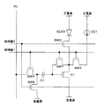
すなわち、図2に示すように、本実施形態の画素回路は、被駆動素子である有機EL素子OLEDと、これに電流を供給するドライブトランジスタT1と、信号電圧を充電する書込みトランジスタSW4と、信号電圧を保持する容量C1と、ある一定の外部参照電流IrをT1にプログラムするためのスイッチSW1,SW2,SW3とから構成されている。 That is, as shown in FIG. 2, the pixel circuit of the present embodiment includes an organic EL element OLED that is a driven element, a drive transistor T1 that supplies current to the organic EL element OLED, a write transistor SW4 that charges a signal voltage, The capacitor C1 that holds the voltage and switches SW1, SW2, and SW3 for programming a certain external reference current Ir to T1.
ドライブトランジスタT1のゲートは、容量C1を介してスイッチSW4の一端に接続される。スイッチSW4の他端、画素の表示階調を示す信号電圧が供給される信号線DLに接続される。従って、スイッチSW4をオンすることで信号電圧がドライブトランジスタT1のゲートに書き込まれる。スイッチSW1は、書き込みトランジスタT1のゲートとドレインの間に設けられ、スイッチSW1をオンすることで、書き込みトランジスタT1のゲートドレイン間が短絡される。 The gate of the drive transistor T1 is connected to one end of the switch SW4 via the capacitor C1. The other end of the switch SW4 is connected to a signal line DL to which a signal voltage indicating the display gradation of the pixel is supplied. Therefore, the signal voltage is written to the gate of the drive transistor T1 by turning on the switch SW4. The switch SW1 is provided between the gate and drain of the write transistor T1, and the gate and drain of the write transistor T1 are short-circuited by turning on the switch SW1.
また、スイッチSW2は、ドライブトランジスタT1のドレイン(またはソース)と有機EL素子OLEDとの間に設けられ、スイッチSW2をオンすることでドライブトランジスタT1のドレイン電流が有機EL素子OLEDに流れる。スイッチSW3はドライブトランジスタT1のドレイン(またはソース)と定電流源CC1との間に設けられ、スイッチSW3をオンすることで、定電流源CC1からの定電流IrがトランジスタT1のドレイン(またはソース)に供給される。 The switch SW2 is provided between the drain (or source) of the drive transistor T1 and the organic EL element OLED, and the drain current of the drive transistor T1 flows to the organic EL element OLED by turning on the switch SW2. The switch SW3 is provided between the drain (or source) of the drive transistor T1 and the constant current source CC1, and by turning on the switch SW3, the constant current Ir from the constant current source CC1 is changed to the drain (or source) of the transistor T1. To be supplied.
このような回路において、スイッチSW1,SW3をオン、スイッチSW2をオフにする。これによって、ドライブトランジスタT1のゲートドレイン間が短絡され、その状態でドライブトランジスタT1のドレインにIrが供給されるため、その定電流Irが負電源に向けて流れる。そして、このようにドライブトランジスタT1のゲートドレイン間を短絡して電流Irを流すことで、ドライブトランジスタT1のゲート・ソース間にドレイン電流Irに対応する電圧Vrが蓄えられる。すなわち、ドライブトランジスタT1のゲート電圧は負電源の電圧より電圧Vrだけ高い電圧になる。電圧Vrは個々のドライブトランジスタT1の特性により異なるため、通常典型的な値VroからdVrだけずれる。すなわち、Vr=Vro+dVrとなる。 In such a circuit, the switches SW1 and SW3 are turned on and the switch SW2 is turned off. As a result, the gate and drain of the drive transistor T1 are short-circuited, and Ir is supplied to the drain of the drive transistor T1 in this state, so that the constant current Ir flows toward the negative power source. By thus short-circuiting the gate and drain of the drive transistor T1 and causing the current Ir to flow, the voltage Vr corresponding to the drain current Ir is stored between the gate and source of the drive transistor T1. That is, the gate voltage of the drive transistor T1 is higher than the negative power supply voltage by the voltage Vr. Since the voltage Vr varies depending on the characteristics of the individual drive transistors T1, it is usually shifted from the typical value Vro by dVr. That is, Vr = Vro + dVr.
次に、スイッチSW1,SW3をオフにし、目的諧調電流Is(有機EL素子OLEDに流したい電流)に対応する目的電圧Vsとするとき、ドライブトランジスタT1のゲート電位がVs−Vroだけ変化するよう、C1のSW4側端子に適当な差分電圧を与える。これにより、ドライブトランジスタT1のゲート・ソース間電圧は目的電圧Vs+dVrになり、ドライブトランジスタT1の特性ばらつきdVr分を補正した電圧がゲート・ソース間に印加される。 Next, when the switches SW1 and SW3 are turned off to obtain the target voltage Vs corresponding to the target gradation current Is (current to be passed through the organic EL element OLED), the gate potential of the drive transistor T1 is changed by Vs−Vro. An appropriate differential voltage is applied to the SW4 side terminal of C1. As a result, the gate-source voltage of the drive transistor T1 becomes the target voltage Vs + dVr, and a voltage obtained by correcting the characteristic variation dVr of the drive transistor T1 is applied between the gate and the source.
最後に、スイッチSW2をオンにして目的電流Isを有機EL素子OLEDに流して発光させる。 Finally, the switch SW2 is turned on to cause the target current Is to flow through the organic EL element OLED to emit light.
ここで、ドライブトランジスタT1のドレイン電流Idとゲート・ソース間電圧Vgsの関係を
Id=f(Vgs)=uCW/L*(Vgs−Vth)2・・・(1)
とすると、あるドライブトランジスタTiのIdi−Vgsの関係fiは、
Idi=fi(Vgs)=ki*fo(Vgs−dVthi)・・・(2)
となる。ただし、uは移動度、Cはゲート容量、W,Lはそれぞれトランジスタのチャネル幅、およびチャネル長である。ここで、foは典型的なId−Vgs関数、fiは典型的な関数foからのばらつきを含んでいることを意味し、kiはTiの移動度の典型値に対する比、dVthiはTiの閾値の典型値との差である。
Here, the relationship between the drain current Id of the drive transistor T1 and the gate-source voltage Vgs is expressed as follows: Id = f (Vgs) = uCW / L * (Vgs−Vth) 2 (1)
Then, the relationship fi of Idi-Vgs of a certain drive transistor Ti is
Idi = fi (Vgs) = ki * fo (Vgs−dVthi) (2)
It becomes. Where u is the mobility, C is the gate capacitance, and W and L are the channel width and channel length of the transistor, respectively. Here, fo means a typical Id-Vgs function, fi means a variation from the typical function fo, ki is a ratio of Ti to a typical value, and dVthi is a Ti threshold value. It is the difference from the typical value.
定電流Irをプログラミングした際のTiのI−V関係は、
Ir=fi(Vri)=ki*fo(Vri−dVthi)・・・(3)
となる。ただし、VriはTiにIrを流したときのゲート・ソース間電圧である。
The IV relationship of Ti when programming the constant current Ir is
Ir = fi (Vri) = ki * fo (Vri−dVthi) (3)
It becomes. Vri is a gate-source voltage when Ir is passed through Ti.
一方、foには逆関数が存在し、これをfo(−1)とすると、上記式(3)は、
Vri−dVthi=fo(−1)(Ir/ki)・・・(4)
と表せる。同様に、典型的なドライブトランジスタToについては、
Vro=fo(−1)(Ir)・・・(5)
と表せる。
On the other hand, an inverse function exists in fo, and when this is fo (−1), the above equation (3) is
Vri−dVthi = fo (−1) (Ir / ki) (4)
It can be expressed. Similarly, for a typical drive transistor To:
Vro = fo (-1) (Ir) (5)
It can be expressed.
従って、容量C1を介して目的信号電圧Vsと典型的参照電圧Vroの差分電圧Vs−Vroを上記で蓄えたVriに加算すると、ドライブトランジスタTiのドレイン電流Iiは、
Ii=fi(Vgsi)=fi(Vs−Vro+Vri)
=ki*fo(Vs−Vro+Vri−dVthi)・・・(6)
となる。
Therefore, when the difference voltage Vs−Vro between the target signal voltage Vs and the typical reference voltage Vro is added to the Vri stored above through the capacitor C1, the drain current Ii of the drive transistor Ti is
Ii = fi (Vgsi) = fi (Vs−Vro + Vri)
= Ki * fo (Vs−Vro + Vri−dVthi) (6)
It becomes.
従って、式(4)、(5)より、
Ii=ki*fo{Vs−fo(−1)(Ir)+fo(−1)(Ir/ki)}
・・・(7)
となる。
Therefore, from the equations (4) and (5),
Ii = ki * fo {Vs−fo (−1) (Ir) + fo (−1) (Ir / ki)}
... (7)
It becomes.
従来の2トランジスタの回路の場合(2)と比べると、dVthiの影響が消え、さらにkiのばらつきの影響も抑えられており、従来の場合に比べてTiを流れる電流のばらつきが抑えられる事がわかる。 Compared with the case of the conventional two-transistor circuit (2), the influence of dVthi disappears and the influence of the variation of ki is also suppressed, and the variation of the current flowing through Ti can be suppressed compared to the conventional case. Recognize.
なお、信号線に供給される信号電圧は、RGB別の輝度信号などから形成される信号である。従って、この輝度信号を信号電圧Vs−Vroに変換すればよい。 The signal voltage supplied to the signal line is a signal formed from a luminance signal for each RGB. Therefore, the luminance signal may be converted into the signal voltage Vs-Vro.
「具体的構成」
上述の図2の構成については、定電流Irのプログラミング方法と差分電圧Vs−Vroの書込み方法によって種々の回路構成と駆動方法が考えられる。
"Specific composition"
Regarding the configuration of FIG. 2 described above, various circuit configurations and driving methods are conceivable depending on the programming method of the constant current Ir and the writing method of the differential voltage Vs-Vro.
以下に、いくつか実施例を挙げるがこれらに限定されるべきものではない。また、これらの実施例には、例としてNチャネル型のTFTをドライブトランジスタとして採用しているが、Pチャネル型でも電流の正負を換えることで全く同じ効果を得ることができる。 Some examples are given below, but should not be construed as being limited thereto. In these embodiments, an N-channel TFT is used as a drive transistor as an example, but the same effect can be obtained by changing the polarity of the current even in the P-channel type.
(具体例1)
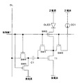
図3に、本発明の駆動を実現する回路の一具体例を示す。図2と同様に、ドライブトランジスタT1のドレインと、そのゲート、有機EL素子OLEDのカソード、定電流源CC1との間に、それぞれSW1、SW2、SW3を挿入配置すると共に、容量C1と信号線との間にスイッチSW4を設けている。さらに、この図3の例では、スイッチSW4と容量C1との接続点がスイッチSW5を介して負電源に接続されている。
(Specific example 1)
FIG. 3 shows a specific example of a circuit for realizing the driving of the present invention. As in FIG. 2, SW1, SW2, and SW3 are inserted between the drain of the drive transistor T1, its gate, the cathode of the organic EL element OLED, and the constant current source CC1, respectively, and the capacitor C1 and the signal line A switch SW4 is provided between the two. Further, in the example of FIG. 3, the connection point between the switch SW4 and the capacitor C1 is connected to the negative power source via the switch SW5.
また、スイッチSW1〜SW5は、すべてnチャネルTFTで構成されており、スイッチSW1,SW3,SW4のゲートは制御線1、スイッチSW2のゲートは制御線2、スイッチSW5のゲートは制御線3に接続されている。 The switches SW1 to SW5 are all composed of n-channel TFTs. The gates of the switches SW1, SW3 and SW4 are connected to the control line 1, the gate of the switch SW2 is connected to the control line 2, and the gate of the switch SW5 is connected to the control line 3. Has been.
この回路において、制御線1をHレベルとしスイッチSW1,SW3,SW4をオン、制御線2,3をLレベルとしてスイッチSW2,SW5をオフにする。これによって、ドライブトランジスタT1のゲートに定電流Irに対応する電圧をプログラミング(対応する電圧Vrをセット)する。このとき、スイッチSW4はオンになっており、容量C1のスイッチSW4側には、−(Vs−Vro)の電圧を信号線DLから印加しておく。このため、容量C1には、Vr−(Vs−Vro)の電圧が充電される。 In this circuit, the control line 1 is set to H level, the switches SW1, SW3, SW4 are turned on, the control lines 2, 3 are set to L level, and the switches SW2, SW5 are turned off. As a result, a voltage corresponding to the constant current Ir is programmed (a corresponding voltage Vr is set) at the gate of the drive transistor T1. At this time, the switch SW4 is turned on, and a voltage of − (Vs−Vro) is applied from the signal line DL to the switch SW4 side of the capacitor C1. Therefore, the capacitor C1 is charged with a voltage of Vr− (Vs−Vro).
次に、制御線1をLレベル、制御線3をHレベルにする。これによって、スイッチSW1,SW3,SW4がオフ、スイッチSW5がオンになるので、スイッチSW4と容量C1との接続点の電圧は、−(Vs−Vro)→0(負電源電圧0V)に変化する。このため、容量C1のドライブトランジスタT1側端子(ゲート)には、Vs−Vroが加算される。これによって、ドライブトランジスタT1のゲートは、Vs−Vro+Vrとなる。そして、スイッチSW2をオンすることで、ドライブトランジスタT1のゲート電圧Vs−Vro+Vrに応じた電流が有機EL素子OLEDに供給される。なお、ここでのVrは、1つの画素のドライブトランジスタT1についてのVrであり、Vriである。 Next, the control line 1 is set to L level and the control line 3 is set to H level. As a result, the switches SW1, SW3, and SW4 are turned off and the switch SW5 is turned on, so that the voltage at the connection point between the switch SW4 and the capacitor C1 changes from − (Vs−Vro) → 0 (negative power supply voltage 0 V). . Therefore, Vs−Vro is added to the drive transistor T1 side terminal (gate) of the capacitor C1. As a result, the gate of the drive transistor T1 becomes Vs−Vro + Vr. Then, by turning on the switch SW2, a current corresponding to the gate voltage Vs−Vro + Vr of the drive transistor T1 is supplied to the organic EL element OLED. Here, Vr is Vr for the drive transistor T1 of one pixel, and is Vri.
図4にそれぞれのスイッチのオン・オフのタイミングを図示する。このように、スイッチSW1,SW3,SW4をオンする時に、スイッチSW2,SW5をオフしておく。これによって、ゲート電圧をVrにセットするプログラミングが行われ、また容量の充電量をVs−Vro+Vriとする。そして、スイッチSW1,SW3,SW4をオフし、スイッチSW5をオンすることで、容量C1の充電電圧が確定する。その後、スイッチSW2をオンすることで有機EL素子OLEDが発光する。なお、スイッチSW2のオンをスイッチSW5のオンなどより遅らせることによって、容量C1の充電電圧の変化を抑制することができる。 FIG. 4 shows the on / off timing of each switch. Thus, when the switches SW1, SW3 and SW4 are turned on, the switches SW2 and SW5 are turned off. Thereby, programming for setting the gate voltage to Vr is performed, and the charge amount of the capacitor is set to Vs−Vro + Vri. Then, the switches SW1, SW3, SW4 are turned off and the switch SW5 is turned on, so that the charging voltage of the capacitor C1 is determined. Thereafter, the organic EL element OLED emits light by turning on the switch SW2. Note that a change in the charging voltage of the capacitor C1 can be suppressed by delaying the turning on of the switch SW2 from the turning on of the switch SW5.
図5は、スイッチSW2,SW5を同一の制御線3に接続したものである。この場合には、図6のように制御線1,3を制御することで、上述の図3と同様の動作が達成される。なお、この図5の構成は、制御線が少なくてよいが、スイッチSW2が、スイッチSW5より先にオンすると、容量C1に充電された電荷が逃げ、ドライブトランジスタT1のゲート電圧が変動しやすいという問題がある。 In FIG. 5, the switches SW2 and SW5 are connected to the same control line 3. In this case, by controlling the control lines 1 and 3 as shown in FIG. 6, the same operation as that of FIG. 3 is achieved. Although the configuration of FIG. 5 requires fewer control lines, when the switch SW2 is turned on before the switch SW5, the charge charged in the capacitor C1 escapes and the gate voltage of the drive transistor T1 is likely to fluctuate. There's a problem.
図7は、スイッチSW1,SW3,SW4をnチャネル、スイッチSW2,SW5をPチャネルとし、1つの制御線1によりすべてのスイッチSW1〜SW5のスイッチングを行うものである。この例の動作は、図5の場合と同様である。 In FIG. 7, the switches SW1, SW3 and SW4 are n-channel, and the switches SW2 and SW5 are P-channel, and all the switches SW1 to SW5 are switched by one control line 1. The operation of this example is the same as in FIG.
図8は、ドライブトランジスタT1のソースにスイッチSW3を介し定電流源CC1を接続すると共に、スイッチSW2を介し有機EL素子OLEDのアノードを接続したものである。なお、有機EL素子OLEDのカソードは、負電源に接続している。 In FIG. 8, the constant current source CC1 is connected to the source of the drive transistor T1 via the switch SW3, and the anode of the organic EL element OLED is connected via the switch SW2. The cathode of the organic EL element OLED is connected to a negative power source.
このような回路によって、上述の図5の回路と同様に動作する。すなわち、スイッチSW1,SW3,SW4をオン、スイッチSW2,SW5をオフして、ドライブトランジスタT1のゲートに定電流に応じた電圧をセットし、その後スイッチSW1,SW3,SW4をオフ、スイッチSW5をオンして、ドライブトランジスタT1のゲート電圧を確定する。そして、スイッチSW2をオンして有機EL素子OLEDが発光する。 Such a circuit operates in the same manner as the circuit shown in FIG. That is, the switches SW1, SW3, and SW4 are turned on, the switches SW2 and SW5 are turned off, the voltage corresponding to the constant current is set to the gate of the drive transistor T1, and then the switches SW1, SW3, and SW4 are turned off and the switch SW5 is turned on. Then, the gate voltage of the drive transistor T1 is determined. Then, the switch SW2 is turned on and the organic EL element OLED emits light.
図9は、ドライブトランジスタT1にpチャネルTFTを用いた例である。この例では、プログラミング期間において、ドライブトランジスタT1のゲートに正電源電圧VDD−Vrの電圧が蓄積され、これから(Vs−Vro)の差分電圧が減算される。そこで、目標電圧を電源電圧から減算する極性が反対(電圧が低いほど輝度が高い)の信号とすることで同様の動作が得られる。 FIG. 9 shows an example in which a p-channel TFT is used for the drive transistor T1. In this example, in the programming period, the voltage of the positive power supply voltage VDD−Vr is accumulated in the gate of the drive transistor T1, and the difference voltage of (Vs−Vro) is subtracted therefrom. Therefore, a similar operation can be obtained by using a signal having the opposite polarity (the luminance is higher as the voltage is lower) for subtracting the target voltage from the power supply voltage.
ここで、上記実施形態においては、1画素回路についてのみ示した。しかし、表示装置は、この画素をマトリクス状に配置して、各画素の表示を制御することで全体としての表示が行える。通常の場合、1水平ラインのすべての画素について、上述のような動作を同時に行う。そこで、水平方向の制御線を1本または2本設けることで上述のような制御が行える。一方、各画素の表示についての輝度信号(ビデオ信号)は、点順次で供給されることが普通であり、このビデオ信号に対応する信号電圧は各信号線に順次セットしてもよいし、1ライン分信号電圧をセットした後、全信号線に一度に信号電圧を供給してもよい。 Here, in the above embodiment, only one pixel circuit is shown. However, the display device can perform display as a whole by arranging the pixels in a matrix and controlling the display of each pixel. In a normal case, the above-described operation is simultaneously performed for all the pixels in one horizontal line. Therefore, the control as described above can be performed by providing one or two horizontal control lines. On the other hand, the luminance signal (video signal) for the display of each pixel is usually supplied in a dot-sequential manner, and the signal voltage corresponding to this video signal may be sequentially set on each signal line. After setting the signal voltage for the line, the signal voltage may be supplied to all the signal lines at once.
C1 容量、CC1 定電流源、DL 信号線、OLED 有機EL素子、SW1〜SW5 スイッチ、T1 ドライブトランジスタ、T2 書き込みトランジスタ。 C1 capacity, CC1 constant current source, DL signal line, OLED organic EL element, SW1 to SW5 switch, T1 drive transistor, T2 write transistor.
Claims (12)
前記駆動トランジスタに実質一定の電流を流すゲート・ソース間電圧を印加するゲート・ソース間電圧印加手段と、
前記駆動トランジスタのゲート・ソース間電圧に所定の信号電圧を加算する加算手段と、
を有する駆動回路。 A drive circuit for a light-emitting element, including a drive transistor that controls a drive current to a light-emitting element driven by a current,
Gate-source voltage applying means for applying a gate-source voltage for flowing a substantially constant current to the drive transistor;
Adding means for adding a predetermined signal voltage to the gate-source voltage of the driving transistor;
A driving circuit having:
前記ゲート・ソース間電圧印加手段は、
外部に設けた定電流源からの定電流を受け入れる定電流受け入れ手段と、
前記駆動トランジスタのドレイン・ゲート間をショートするスイッチと、
前記駆動トランジスタのドレインまたはソースの一方と、発光素子または定電流源との間の接続を切り替える切り替え手段と、
を有する駆動回路。 The circuit of claim 1, wherein
The gate-source voltage applying means includes:
A constant current receiving means for receiving a constant current from an external constant current source;
A switch for short-circuiting between the drain and gate of the driving transistor;
Switching means for switching a connection between one of the drain or source of the driving transistor and a light emitting element or a constant current source;
A driving circuit having:
前記スイッチと、前記切り替え手段がいずれも薄膜トランジスタである駆動回路。 The circuit of claim 2, wherein
A drive circuit in which the switch and the switching means are both thin film transistors.
前記切り替え手段がダイオードを含み、このダイオードを順バイアスでオン、逆バイアスでオフさせて接続を切り替える駆動回路。 The circuit of claim 2, wherein
A drive circuit in which the switching means includes a diode, and the connection is switched by turning on the diode with a forward bias and turning it off with a reverse bias.
前記スイッチと、前記切り替え手段の前記ダイオード以外の構成がいずれも薄膜トランジスタである駆動回路。 The circuit of claim 4, wherein
A drive circuit in which the configuration other than the switch and the diode of the switching means is a thin film transistor.
外部に設けた定電流源が、外付けのドライバICである駆動回路。 In the circuit according to any one of claims 2 to 5,
A drive circuit in which an external constant current source is an external driver IC.
外部に設けた定電流源が、基板上に形成された単一もしくは複数の薄膜トランジスタで構成されている駆動回路。 In the circuit according to any one of claims 2 to 5,
A drive circuit in which a constant current source provided outside is composed of a single or a plurality of thin film transistors formed on a substrate.
発光素子が有機EL素子である駆動回路。 In the circuit according to any one of claims 1 to 7,
A driving circuit in which the light emitting element is an organic EL element.
前記加算手段は、
一方の端子を駆動トランジスタのゲートに接続した容量についてその他方の端子電位を目的の信号電圧分だけ変化させる駆動回路。 The circuit according to any one of claims 1 to 8,
The adding means includes
A drive circuit that changes the potential of the other terminal of a capacitor having one terminal connected to the gate of a drive transistor by an amount corresponding to a target signal voltage.
前記容量の端子電圧の変化は、その端子に接続される信号線電位を変化させる駆動回路。 The circuit of claim 9, wherein
The drive circuit for changing the terminal voltage of the capacitor changes the potential of the signal line connected to the terminal.
前記容量の端子電圧の変化は、端子の接続先を、所定電位の信号線と、基準電位線の間で切り替えることで行う駆動回路。 The circuit of claim 9, wherein
A drive circuit that changes the terminal voltage of the capacitor by switching the connection destination of the terminal between a signal line having a predetermined potential and a reference potential line.
前記駆動トランジスタのゲート・ソース間に一定電流に対応する電圧を印加するために要する時間が、信号線から信号電圧を容量に印加するために要する時間に等しい駆動回路。 The circuit according to claim 10 or 11,
A drive circuit in which a time required to apply a voltage corresponding to a constant current between a gate and a source of the drive transistor is equal to a time required to apply a signal voltage from a signal line to a capacitor.
Priority Applications (2)
| Application Number | Priority Date | Filing Date | Title |
|---|---|---|---|
| JP2005108219A JP2006285116A (en) | 2005-04-05 | 2005-04-05 | Driving circuit |
| US11/385,070 US7995008B2 (en) | 2005-04-05 | 2006-03-21 | Drive circuit for electroluminescent device |
Applications Claiming Priority (1)
| Application Number | Priority Date | Filing Date | Title |
|---|---|---|---|
| JP2005108219A JP2006285116A (en) | 2005-04-05 | 2005-04-05 | Driving circuit |
Publications (2)
| Publication Number | Publication Date |
|---|---|
| JP2006285116A true JP2006285116A (en) | 2006-10-19 |
| JP2006285116A5 JP2006285116A5 (en) | 2007-02-08 |
Family
ID=37069788
Family Applications (1)
| Application Number | Title | Priority Date | Filing Date |
|---|---|---|---|
| JP2005108219A Pending JP2006285116A (en) | 2005-04-05 | 2005-04-05 | Driving circuit |
Country Status (2)
| Country | Link |
|---|---|
| US (1) | US7995008B2 (en) |
| JP (1) | JP2006285116A (en) |
Cited By (9)
| Publication number | Priority date | Publication date | Assignee | Title |
|---|---|---|---|---|
| JP2007323040A (en) * | 2006-06-01 | 2007-12-13 | Lg Philips Lcd Co Ltd | Organic light-emitting diode display device and driving method thereof |
| JP2008233461A (en) * | 2007-03-20 | 2008-10-02 | Seiko Epson Corp | Pixel circuit, electrooptical device, and electronic equipment |
| JP2009058621A (en) * | 2007-08-30 | 2009-03-19 | Kyocera Corp | Image display device, and method for driving image display device |
| JP2011520139A (en) * | 2008-04-18 | 2011-07-14 | イグニス・イノベーション・インコーポレイテッド | System and driving method for light emitting device display |
| JP2011170181A (en) * | 2010-02-19 | 2011-09-01 | Seiko Epson Corp | Light emitting device, method for driving light emitting device, and electronic apparatus |
| JP2013511061A (en) * | 2009-11-12 | 2013-03-28 | イグニス・イノベイション・インコーポレーテッド | Efficient programming and fast calibration for light-emitting displays and their stable current sources and sinks |
| JP2014006893A (en) * | 2012-06-01 | 2014-01-16 | Semiconductor Energy Lab Co Ltd | Semiconductor device and method of driving the same |
| KR101502070B1 (en) * | 2008-12-02 | 2015-03-12 | 삼성디스플레이 주식회사 | Display device and driving method thereof |
| CN105139802A (en) * | 2015-09-10 | 2015-12-09 | 中国科学院上海高等研究院 | AMOLED pixel driving circuit and method realizing voltage and current mixed programming |
Families Citing this family (39)
| Publication number | Priority date | Publication date | Assignee | Title |
|---|---|---|---|---|
| CA2490858A1 (en) | 2004-12-07 | 2006-06-07 | Ignis Innovation Inc. | Driving method for compensated voltage-programming of amoled displays |
| JP5355080B2 (en) | 2005-06-08 | 2013-11-27 | イグニス・イノベイション・インコーポレーテッド | Method and system for driving a light emitting device display |
| US9489891B2 (en) | 2006-01-09 | 2016-11-08 | Ignis Innovation Inc. | Method and system for driving an active matrix display circuit |
| EP1971975B1 (en) | 2006-01-09 | 2015-10-21 | Ignis Innovation Inc. | Method and system for driving an active matrix display circuit |
| US9269322B2 (en) | 2006-01-09 | 2016-02-23 | Ignis Innovation Inc. | Method and system for driving an active matrix display circuit |
| KR100821055B1 (en) * | 2006-12-27 | 2008-04-08 | 삼성에스디아이 주식회사 | Organic light emitting diodes display device and method of the same |
| CN100561552C (en) * | 2007-03-28 | 2009-11-18 | 中国科学院微电子研究所 | The fault tolerable circuit that is used for display of organic electroluminescence or illuminating device |
| JP5096103B2 (en) * | 2007-10-19 | 2012-12-12 | グローバル・オーエルイーディー・テクノロジー・リミテッド・ライアビリティ・カンパニー | Display device |
| JP5073544B2 (en) * | 2008-03-26 | 2012-11-14 | 富士フイルム株式会社 | Display device |
| CA2637343A1 (en) | 2008-07-29 | 2010-01-29 | Ignis Innovation Inc. | Improving the display source driver |
| US8215171B1 (en) * | 2008-08-26 | 2012-07-10 | University Of South Florida | Uniform mass sensitivity thickness shear mode quartz resonator |
| US9370075B2 (en) | 2008-12-09 | 2016-06-14 | Ignis Innovation Inc. | System and method for fast compensation programming of pixels in a display |
| MY149776A (en) * | 2009-02-20 | 2013-10-14 | Lynch John | Memory architecture with a current controller and reduced power requirements |
| JP5284198B2 (en) * | 2009-06-30 | 2013-09-11 | キヤノン株式会社 | Display device and driving method thereof |
| JP5491835B2 (en) * | 2009-12-02 | 2014-05-14 | グローバル・オーエルイーディー・テクノロジー・リミテッド・ライアビリティ・カンパニー | Pixel circuit and display device |
| CA2687631A1 (en) | 2009-12-06 | 2011-06-06 | Ignis Innovation Inc | Low power driving scheme for display applications |
| CA2696778A1 (en) | 2010-03-17 | 2011-09-17 | Ignis Innovation Inc. | Lifetime, uniformity, parameter extraction methods |
| US9886899B2 (en) | 2011-05-17 | 2018-02-06 | Ignis Innovation Inc. | Pixel Circuits for AMOLED displays |
| US20140368491A1 (en) | 2013-03-08 | 2014-12-18 | Ignis Innovation Inc. | Pixel circuits for amoled displays |
| US9351368B2 (en) | 2013-03-08 | 2016-05-24 | Ignis Innovation Inc. | Pixel circuits for AMOLED displays |
| JP2014522506A (en) | 2011-05-28 | 2014-09-04 | イグニス・イノベイション・インコーポレーテッド | System and method for fast compensation programming of display pixels |
| US9747834B2 (en) | 2012-05-11 | 2017-08-29 | Ignis Innovation Inc. | Pixel circuits including feedback capacitors and reset capacitors, and display systems therefore |
| US9336717B2 (en) | 2012-12-11 | 2016-05-10 | Ignis Innovation Inc. | Pixel circuits for AMOLED displays |
| US9786223B2 (en) | 2012-12-11 | 2017-10-10 | Ignis Innovation Inc. | Pixel circuits for AMOLED displays |
| CA2894717A1 (en) | 2015-06-19 | 2016-12-19 | Ignis Innovation Inc. | Optoelectronic device characterization in array with shared sense line |
| US9721505B2 (en) | 2013-03-08 | 2017-08-01 | Ignis Innovation Inc. | Pixel circuits for AMOLED displays |
| CN103236236A (en) * | 2013-04-24 | 2013-08-07 | 京东方科技集团股份有限公司 | Pixel driving circuit, array substrate and display device |
| KR102068589B1 (en) * | 2013-12-30 | 2020-01-21 | 엘지디스플레이 주식회사 | Organic light emitting display device and method for driving thereof |
| CN103985360B (en) * | 2014-05-04 | 2016-04-27 | 深圳市华星光电技术有限公司 | The driving circuit of display panel and liquid crystal indicator |
| CA2873476A1 (en) | 2014-12-08 | 2016-06-08 | Ignis Innovation Inc. | Smart-pixel display architecture |
| CA2886862A1 (en) | 2015-04-01 | 2016-10-01 | Ignis Innovation Inc. | Adjusting display brightness for avoiding overheating and/or accelerated aging |
| CA2898282A1 (en) | 2015-07-24 | 2017-01-24 | Ignis Innovation Inc. | Hybrid calibration of current sources for current biased voltage progra mmed (cbvp) displays |
| US10657895B2 (en) | 2015-07-24 | 2020-05-19 | Ignis Innovation Inc. | Pixels and reference circuits and timing techniques |
| US10373554B2 (en) | 2015-07-24 | 2019-08-06 | Ignis Innovation Inc. | Pixels and reference circuits and timing techniques |
| CA2908285A1 (en) | 2015-10-14 | 2017-04-14 | Ignis Innovation Inc. | Driver with multiple color pixel structure |
| CN105609050B (en) * | 2016-01-04 | 2018-03-06 | 京东方科技集团股份有限公司 | pixel compensation circuit and AMOLED display device |
| KR101856378B1 (en) * | 2016-10-31 | 2018-06-20 | 엘지디스플레이 주식회사 | Organic light emitting diode display device and the method for driving the same |
| US10497310B2 (en) * | 2018-03-23 | 2019-12-03 | Sharp Kabushiki Kaisha | TFT compensation circuit for display device using reference current |
| CN111968585B (en) * | 2020-08-27 | 2021-12-07 | 京东方科技集团股份有限公司 | Pixel circuit, pixel driving method and display device |
Citations (4)
| Publication number | Priority date | Publication date | Assignee | Title |
|---|---|---|---|---|
| JP2004341444A (en) * | 2003-05-19 | 2004-12-02 | Sony Corp | Pixel circuit, display device, and method for driving pixel circuit |
| JP2005141163A (en) * | 2003-11-10 | 2005-06-02 | Sony Corp | Pixel circuit, display device, and method for driving pixel circuit |
| JP2005292436A (en) * | 2004-03-31 | 2005-10-20 | Nec Corp | Electric circuit, driving method for the same, pixel circuit of display apparatus, display apparatus and driving method for the same |
| JP2008521033A (en) * | 2004-11-16 | 2008-06-19 | イグニス・イノベイション・インコーポレーテッド | System and driving method for active matrix light emitting device display |
Family Cites Families (5)
| Publication number | Priority date | Publication date | Assignee | Title |
|---|---|---|---|---|
| JP2001147659A (en) * | 1999-11-18 | 2001-05-29 | Sony Corp | Display device |
| US20050180083A1 (en) * | 2002-04-26 | 2005-08-18 | Toshiba Matsushita Display Technology Co., Ltd. | Drive circuit for el display panel |
| JP2005049430A (en) * | 2003-07-30 | 2005-02-24 | Hitachi Ltd | Image display device |
| JP2005084119A (en) * | 2003-09-04 | 2005-03-31 | Nec Corp | Driving circuit for light emitting element and current controlled light emission display device |
| CN101329766B (en) | 2007-06-18 | 2012-05-30 | 索尼(中国)有限公司 | Apparatus, method and system for analyzing mobile image |
-
2005
- 2005-04-05 JP JP2005108219A patent/JP2006285116A/en active Pending
-
2006
- 2006-03-21 US US11/385,070 patent/US7995008B2/en active Active
Patent Citations (4)
| Publication number | Priority date | Publication date | Assignee | Title |
|---|---|---|---|---|
| JP2004341444A (en) * | 2003-05-19 | 2004-12-02 | Sony Corp | Pixel circuit, display device, and method for driving pixel circuit |
| JP2005141163A (en) * | 2003-11-10 | 2005-06-02 | Sony Corp | Pixel circuit, display device, and method for driving pixel circuit |
| JP2005292436A (en) * | 2004-03-31 | 2005-10-20 | Nec Corp | Electric circuit, driving method for the same, pixel circuit of display apparatus, display apparatus and driving method for the same |
| JP2008521033A (en) * | 2004-11-16 | 2008-06-19 | イグニス・イノベイション・インコーポレーテッド | System and driving method for active matrix light emitting device display |
Cited By (13)
| Publication number | Priority date | Publication date | Assignee | Title |
|---|---|---|---|---|
| JP2007323040A (en) * | 2006-06-01 | 2007-12-13 | Lg Philips Lcd Co Ltd | Organic light-emitting diode display device and driving method thereof |
| JP2008233461A (en) * | 2007-03-20 | 2008-10-02 | Seiko Epson Corp | Pixel circuit, electrooptical device, and electronic equipment |
| JP2009058621A (en) * | 2007-08-30 | 2009-03-19 | Kyocera Corp | Image display device, and method for driving image display device |
| JP2014029533A (en) * | 2008-04-18 | 2014-02-13 | Ignis Innovation Inc | System and driving method for light emitting device display |
| JP2011520139A (en) * | 2008-04-18 | 2011-07-14 | イグニス・イノベーション・インコーポレイテッド | System and driving method for light emitting device display |
| US10555398B2 (en) | 2008-04-18 | 2020-02-04 | Ignis Innovation Inc. | System and driving method for light emitting device display |
| US9064454B2 (en) | 2008-12-02 | 2015-06-23 | Samsung Display Co., Ltd. | Display device and method of driving the same |
| KR101502070B1 (en) * | 2008-12-02 | 2015-03-12 | 삼성디스플레이 주식회사 | Display device and driving method thereof |
| JP2013511061A (en) * | 2009-11-12 | 2013-03-28 | イグニス・イノベイション・インコーポレーテッド | Efficient programming and fast calibration for light-emitting displays and their stable current sources and sinks |
| JP2011170181A (en) * | 2010-02-19 | 2011-09-01 | Seiko Epson Corp | Light emitting device, method for driving light emitting device, and electronic apparatus |
| JP2014006893A (en) * | 2012-06-01 | 2014-01-16 | Semiconductor Energy Lab Co Ltd | Semiconductor device and method of driving the same |
| US9916793B2 (en) | 2012-06-01 | 2018-03-13 | Semiconductor Energy Laboratory Co., Ltd. | Semiconductor device and method of driving the same |
| CN105139802A (en) * | 2015-09-10 | 2015-12-09 | 中国科学院上海高等研究院 | AMOLED pixel driving circuit and method realizing voltage and current mixed programming |
Also Published As
| Publication number | Publication date |
|---|---|
| US20060221009A1 (en) | 2006-10-05 |
| US7995008B2 (en) | 2011-08-09 |
Similar Documents
| Publication | Publication Date | Title |
|---|---|---|
| JP2006285116A (en) | Driving circuit | |
| US10957249B2 (en) | Light emitting display device having normal and standby modes and driving method thereof | |
| US9892688B2 (en) | Organic light-emitting display | |
| JP3949040B2 (en) | Driving device for light emitting display panel | |
| JP5163646B2 (en) | Image display device | |
| US8913090B2 (en) | Pixel circuit, organic electro-luminescent display apparatus, and method of driving the same | |
| US8674914B2 (en) | Display device and method of driving the same | |
| KR100637203B1 (en) | An organic light emitting display device and driving method thereof | |
| US20060244688A1 (en) | Organic electroluminescence display device | |
| WO2004109639A1 (en) | Pixel circuit, display device, and method for driving pixel circuit | |
| TWI537922B (en) | Display device | |
| EP1981019A2 (en) | Pixel, organic light emitting display using the same, and associated methods | |
| JP2006011428A (en) | Light emitting display device and method for driving thereof | |
| WO2006103797A1 (en) | Display device and method for driving same | |
| JP2005352411A (en) | Driving circuit for current drive type display element and display apparatus equipped with the same | |
| JP2005134880A (en) | Image display apparatus, driving method thereof, and precharge voltage setting method | |
| JP4913119B2 (en) | Organic electroluminescent display device and driving method thereof | |
| JP2005031643A (en) | Light emitting device and display device | |
| JP5044883B2 (en) | Display device, electric circuit driving method, and display device driving method | |
| JP2011028214A (en) | Pixel driving device, light emitting device, and driving control method for light emitting device | |
| US7864145B2 (en) | Display units and display panels of light emitting display devices | |
| JP5121124B2 (en) | Organic EL pixel circuit | |
| US7746299B2 (en) | Display, array substrate, and method of driving display | |
| JP2005331774A (en) | Current drive pixel circuit | |
| JP4999281B2 (en) | Organic EL pixel circuit |
Legal Events
| Date | Code | Title | Description |
|---|---|---|---|
| A521 | Request for written amendment filed |
Free format text: JAPANESE INTERMEDIATE CODE: A523 Effective date: 20061220 |
|
| A621 | Written request for application examination |
Free format text: JAPANESE INTERMEDIATE CODE: A621 Effective date: 20071211 |
|
| RD03 | Notification of appointment of power of attorney |
Free format text: JAPANESE INTERMEDIATE CODE: A7423 Effective date: 20100319 |
|
| RD04 | Notification of resignation of power of attorney |
Free format text: JAPANESE INTERMEDIATE CODE: A7424 Effective date: 20100512 |
|
| A711 | Notification of change in applicant |
Free format text: JAPANESE INTERMEDIATE CODE: A711 Effective date: 20100520 |
|
| A977 | Report on retrieval |
Free format text: JAPANESE INTERMEDIATE CODE: A971007 Effective date: 20110127 |
|
| A131 | Notification of reasons for refusal |
Free format text: JAPANESE INTERMEDIATE CODE: A131 Effective date: 20110329 |
|
| A521 | Request for written amendment filed |
Free format text: JAPANESE INTERMEDIATE CODE: A523 Effective date: 20110510 |
|
| A02 | Decision of refusal |
Free format text: JAPANESE INTERMEDIATE CODE: A02 Effective date: 20120508 |
|
| A521 | Request for written amendment filed |
Free format text: JAPANESE INTERMEDIATE CODE: A523 Effective date: 20120802 |
|
| A911 | Transfer to examiner for re-examination before appeal (zenchi) |
Free format text: JAPANESE INTERMEDIATE CODE: A911 Effective date: 20120809 |
|
| A912 | Re-examination (zenchi) completed and case transferred to appeal board |
Free format text: JAPANESE INTERMEDIATE CODE: A912 Effective date: 20121130 |