JP5100012B2 - Semiconductor device and manufacturing method thereof - Google Patents
Semiconductor device and manufacturing method thereof Download PDFInfo
- Publication number
- JP5100012B2 JP5100012B2 JP2006013539A JP2006013539A JP5100012B2 JP 5100012 B2 JP5100012 B2 JP 5100012B2 JP 2006013539 A JP2006013539 A JP 2006013539A JP 2006013539 A JP2006013539 A JP 2006013539A JP 5100012 B2 JP5100012 B2 JP 5100012B2
- Authority
- JP
- Japan
- Prior art keywords
- film
- insulating film
- groove
- layer
- conductive film
- Prior art date
- Legal status (The legal status is an assumption and is not a legal conclusion. Google has not performed a legal analysis and makes no representation as to the accuracy of the status listed.)
- Expired - Fee Related
Links
Images


Classifications
-
- H—ELECTRICITY
- H01—ELECTRIC ELEMENTS
- H01L—SEMICONDUCTOR DEVICES NOT COVERED BY CLASS H10
- H01L2224/00—Indexing scheme for arrangements for connecting or disconnecting semiconductor or solid-state bodies and methods related thereto as covered by H01L24/00
- H01L2224/01—Means for bonding being attached to, or being formed on, the surface to be connected, e.g. chip-to-package, die-attach, "first-level" interconnects; Manufacturing methods related thereto
- H01L2224/26—Layer connectors, e.g. plate connectors, solder or adhesive layers; Manufacturing methods related thereto
- H01L2224/31—Structure, shape, material or disposition of the layer connectors after the connecting process
- H01L2224/32—Structure, shape, material or disposition of the layer connectors after the connecting process of an individual layer connector
- H01L2224/321—Disposition
- H01L2224/32135—Disposition the layer connector connecting between different semiconductor or solid-state bodies, i.e. chip-to-chip
- H01L2224/32145—Disposition the layer connector connecting between different semiconductor or solid-state bodies, i.e. chip-to-chip the bodies being stacked
-
- H—ELECTRICITY
- H01—ELECTRIC ELEMENTS
- H01L—SEMICONDUCTOR DEVICES NOT COVERED BY CLASS H10
- H01L2224/00—Indexing scheme for arrangements for connecting or disconnecting semiconductor or solid-state bodies and methods related thereto as covered by H01L24/00
- H01L2224/01—Means for bonding being attached to, or being formed on, the surface to be connected, e.g. chip-to-package, die-attach, "first-level" interconnects; Manufacturing methods related thereto
- H01L2224/42—Wire connectors; Manufacturing methods related thereto
- H01L2224/47—Structure, shape, material or disposition of the wire connectors after the connecting process
- H01L2224/48—Structure, shape, material or disposition of the wire connectors after the connecting process of an individual wire connector
- H01L2224/4805—Shape
- H01L2224/4809—Loop shape
- H01L2224/48091—Arched
-
- H—ELECTRICITY
- H01—ELECTRIC ELEMENTS
- H01L—SEMICONDUCTOR DEVICES NOT COVERED BY CLASS H10
- H01L2224/00—Indexing scheme for arrangements for connecting or disconnecting semiconductor or solid-state bodies and methods related thereto as covered by H01L24/00
- H01L2224/01—Means for bonding being attached to, or being formed on, the surface to be connected, e.g. chip-to-package, die-attach, "first-level" interconnects; Manufacturing methods related thereto
- H01L2224/42—Wire connectors; Manufacturing methods related thereto
- H01L2224/47—Structure, shape, material or disposition of the wire connectors after the connecting process
- H01L2224/48—Structure, shape, material or disposition of the wire connectors after the connecting process of an individual wire connector
- H01L2224/481—Disposition
- H01L2224/48135—Connecting between different semiconductor or solid-state bodies, i.e. chip-to-chip
- H01L2224/48145—Connecting between different semiconductor or solid-state bodies, i.e. chip-to-chip the bodies being stacked
-
- H—ELECTRICITY
- H01—ELECTRIC ELEMENTS
- H01L—SEMICONDUCTOR DEVICES NOT COVERED BY CLASS H10
- H01L2224/00—Indexing scheme for arrangements for connecting or disconnecting semiconductor or solid-state bodies and methods related thereto as covered by H01L24/00
- H01L2224/01—Means for bonding being attached to, or being formed on, the surface to be connected, e.g. chip-to-package, die-attach, "first-level" interconnects; Manufacturing methods related thereto
- H01L2224/42—Wire connectors; Manufacturing methods related thereto
- H01L2224/47—Structure, shape, material or disposition of the wire connectors after the connecting process
- H01L2224/48—Structure, shape, material or disposition of the wire connectors after the connecting process of an individual wire connector
- H01L2224/484—Connecting portions
- H01L2224/48463—Connecting portions the connecting portion on the bonding area of the semiconductor or solid-state body being a ball bond
- H01L2224/48464—Connecting portions the connecting portion on the bonding area of the semiconductor or solid-state body being a ball bond the other connecting portion not on the bonding area also being a ball bond, i.e. ball-to-ball
-
- H—ELECTRICITY
- H01—ELECTRIC ELEMENTS
- H01L—SEMICONDUCTOR DEVICES NOT COVERED BY CLASS H10
- H01L2224/00—Indexing scheme for arrangements for connecting or disconnecting semiconductor or solid-state bodies and methods related thereto as covered by H01L24/00
- H01L2224/73—Means for bonding being of different types provided for in two or more of groups H01L2224/10, H01L2224/18, H01L2224/26, H01L2224/34, H01L2224/42, H01L2224/50, H01L2224/63, H01L2224/71
- H01L2224/732—Location after the connecting process
- H01L2224/73251—Location after the connecting process on different surfaces
- H01L2224/73265—Layer and wire connectors
Description
本発明は、非接触でデータの送受信が可能である半導体装置および当該半導体装置の作製方法に関する。 The present invention relates to a semiconductor device capable of transmitting and receiving data without contact and a method for manufacturing the semiconductor device.
近年、個々の対象物にID(個体識別番号)を与えることで、その対象物の履歴等の情報を明確にし、生産・管理等に役立てるといった個体認識技術が注目されている。その中でも、非接触でデータの送受信が可能な半導体装置の開発が進められている。このような半導体装置として、RFIDタグ(Radio Frequency Identification)(IDタグ、ICタグ、ICチップ、RFタグ(Radio Frequency)、無線タグ、電子タグ、無線チップともよばれる)等が企業内、市場等で導入され始めている。 2. Description of the Related Art In recent years, attention has been focused on an individual recognition technique in which an ID (individual identification number) is given to an individual object to clarify information such as a history of the object and to be useful for production and management. Among them, development of semiconductor devices capable of transmitting and receiving data without contact is underway. As such a semiconductor device, an RFID tag (Radio Frequency Identification) (ID tag, IC tag, IC chip, RF tag (Radio Frequency), wireless tag, electronic tag, also referred to as a wireless chip) is used in an enterprise, a market, or the like. It has begun to be introduced.
現在実用化されているRFIDタグ等の半導体装置の多くは、トランジスタ等から構成される回路を有する素子形成層(IC(Integrated Circuit)チップとも呼ばれる)とアンテナとを有している。これらの半導体装置は、電磁波によってアンテナを介してリーダ/ライタ間とデータのやりとりを行うことができる。 Many semiconductor devices such as RFID tags that are currently in practical use have an element formation layer (also referred to as an IC (Integrated Circuit) chip) having a circuit including a transistor and an antenna. These semiconductor devices can exchange data with a reader / writer via an antenna using electromagnetic waves.
一般的に、上記半導体装置におけるアンテナとして機能する導電膜の形成方法としては、表面積の増加、抵抗の低減を目的とし厚膜化が可能な方法が用いられている。そのため、多くの場合、めっき法を用いることによる導電膜の形成が広く行われている。しかしながら、めっき法でアンテナとして機能する導電膜を形成する場合、形成される導電膜の膜質が十分でないことや、廃液等が生じるため環境等に悪影響をおよぼす等の問題がある。一方、めっき法以外の方法を用いて導電膜を形成する場合、厚膜化が困難であり導電膜の断面積および表面積を十分に確保することが難しいといった問題がある。 In general, as a method for forming a conductive film functioning as an antenna in the semiconductor device, a method capable of increasing the thickness is used for the purpose of increasing the surface area and reducing resistance. Therefore, in many cases, the formation of a conductive film by using a plating method is widely performed. However, when a conductive film that functions as an antenna is formed by a plating method, there are problems such as insufficient film quality of the formed conductive film and adverse effects on the environment and the like due to waste liquid and the like. On the other hand, when a conductive film is formed using a method other than the plating method, there is a problem that it is difficult to increase the film thickness and it is difficult to ensure a sufficient cross-sectional area and surface area of the conductive film.
上記の実情を鑑み、本発明は、アンテナとして十分に機能する導電膜を有する半導体装置および当該半導体装置の作製方法を提供することを目的とする。 In view of the above circumstances, an object of the present invention is to provide a semiconductor device having a conductive film that functions sufficiently as an antenna and a method for manufacturing the semiconductor device.
上記課題を解決するために、本発明では以下の手段を講ずる。 In order to solve the above problems, the present invention takes the following measures.
本発明の半導体装置は、基板上に設けられたトランジスタを含む素子形成層と、素子形成層上に設けられたアンテナとして機能する導電膜とを有し、トランジスタと導電膜は電気的に接続され、導電膜の断面の形状が凹型であることを特徴としている。トランジスタとしては、薄膜トランジスタ(TFT)や電界効果トランジスタ(FET)等を用いることができる。 A semiconductor device of the present invention includes an element formation layer including a transistor provided over a substrate and a conductive film functioning as an antenna provided over the element formation layer, and the transistor and the conductive film are electrically connected to each other. The cross-sectional shape of the conductive film is concave. As the transistor, a thin film transistor (TFT), a field effect transistor (FET), or the like can be used.
また、本発明の半導体装置の他の構成として、基板上に設けられたトランジスタを含む素子形成層と、素子形成層上に設けられた絶縁膜と、絶縁膜上に設けられたアンテナとして機能する導電膜とを有し、トランジスタと導電膜は電気的に接続され、絶縁膜は溝を有し、絶縁膜の表面および溝に沿って導電膜が設けられていることを特徴としている。絶縁膜が有する溝は、絶縁膜を貫通させて設けてもよいし、絶縁膜を貫通させずに絶縁膜に凹部を形成して設けてもよい。溝の構造はどのように設けてもよく、例えば断面がテーパー状等を有するように溝を設けることができる。 As another structure of the semiconductor device of the present invention, the semiconductor device functions as an element formation layer including a transistor provided over a substrate, an insulating film provided over the element formation layer, and an antenna provided over the insulating film. The transistor and the conductive film are electrically connected, the insulating film has a groove, and the conductive film is provided along the surface of the insulating film and the groove. The groove included in the insulating film may be provided so as to penetrate the insulating film, or may be provided so as to form a recess in the insulating film without penetrating the insulating film. The groove structure may be provided in any manner. For example, the groove may be provided so that the cross section has a tapered shape.
また、本発明の半導体装置の他の構成として、基板上に設けられたトランジスタを含む素子形成層と、絶縁膜と導電膜とを含むアンテナ形成層とを有し、絶縁膜は溝を有し、絶縁膜の表面および溝に沿って導電膜が設けられており、トランジスタと導電膜とが導電性微粒子によって電気的に接続されていることを特徴としている。 As another structure of the semiconductor device of the present invention, the semiconductor device includes an element formation layer including a transistor provided over a substrate, and an antenna formation layer including an insulating film and a conductive film, and the insulating film has a groove. A conductive film is provided along the surface of the insulating film and the groove, and the transistor and the conductive film are electrically connected by conductive fine particles.
また、上記半導体装置はRFIDタグ等への利用が可能であり、電磁誘導方式、電磁結合方式またはマイクロ波方式等のいずれの場合にも適用することが可能である。電磁誘導方式および電磁結合方式の場合は、アンテナの形状をコイル状に形成することが好ましい。マイクロ波方式の場合は、受信する電磁波の波長にアンテナの形状が依存するために、使用状況に応じて適宜形状を変えて設けることが好ましい。 The semiconductor device can be used for an RFID tag or the like, and can be applied to any of an electromagnetic induction method, an electromagnetic coupling method, a microwave method, and the like. In the case of the electromagnetic induction method and the electromagnetic coupling method, the antenna is preferably formed in a coil shape. In the case of the microwave method, since the shape of the antenna depends on the wavelength of the electromagnetic wave to be received, it is preferable to change the shape depending on the use situation.
本発明の半導体装置の作製方法として、基板上にトランジスタを含む素子形成層を作製し、素子形成層上に溝を有する絶縁膜を形成し、絶縁膜表面および前記溝に沿うように導電膜を形成し、絶縁膜表面上に形成制された導電膜の一部を選択的に除去することによって導電膜のパターンを形成し、導電膜を覆うように保護膜を形成することを特徴としている。 As a method for manufacturing a semiconductor device of the present invention, an element formation layer including a transistor is formed over a substrate, an insulating film having a groove is formed over the element formation layer, and the conductive film is formed along the insulating film surface and the groove. A conductive film pattern is formed by selectively removing part of the conductive film formed on the surface of the insulating film, and a protective film is formed so as to cover the conductive film.
本発明の半導体装置の他の作製方法として、基板上に剥離層を形成し、剥離層上にトランジスタを含む素子形成層を作製し、素子形成層上に溝を有する絶縁膜を形成し、絶縁膜表面および溝に沿うように導電膜を形成し、絶縁膜表面上に形成された導電膜の一部を選択的に除去することによって導電膜のパターンを形成し、導電膜を覆うように保護膜を形成し、保護膜、絶縁膜および素子形成層を選択的に除去して開口部を設けることにより剥離層を露出させ、開口部にエッチング剤を導入することによって剥離層を除去し、基板から素子形成層を剥離することを特徴としている。 As another method for manufacturing the semiconductor device of the present invention, a separation layer is formed over a substrate, an element formation layer including a transistor is formed over the separation layer, an insulating film having a groove is formed over the element formation layer, and insulation is performed. A conductive film is formed along the film surface and the groove, and a part of the conductive film formed on the surface of the insulating film is selectively removed to form a conductive film pattern so that the conductive film is covered. Forming a film, selectively removing the protective film, the insulating film, and the element formation layer to provide an opening, exposing the peeling layer, and removing the peeling layer by introducing an etchant into the opening; The element forming layer is peeled from the substrate.
本発明の半導体装置の他の作製方法として、第1の基板上に剥離層を形成し、剥離層上にトランジスタを含む素子形成層を作製し、素子形成層上に溝を有する絶縁膜を形成し、絶縁膜表面および溝に沿うように導電膜を形成し、絶縁膜表面上に形成された導電膜の一部を選択的に除去することによって導電膜のパターンを形成し、導電膜を覆うように保護膜を形成し、保護膜、絶縁膜および素子形成層を選択的に除去して開口部を設けることにより剥離層を露出させ、開口部にエッチング剤を導入することによって剥離層の一部を除去し、保護膜表面に第2の基板を貼り合わせることにより設け、物理的手段を用いて第1の基板から素子形成層を剥離することを特徴としている。 As another method for manufacturing a semiconductor device of the present invention, a separation layer is formed over a first substrate, an element formation layer including a transistor is formed over the separation layer, and an insulating film having a groove is formed over the element formation layer. Then, a conductive film is formed along the surface of the insulating film and the groove, and a part of the conductive film formed on the surface of the insulating film is selectively removed to form a conductive film pattern and cover the conductive film Forming a protective film, selectively removing the protective film, the insulating film, and the element formation layer to provide an opening, exposing the peeling layer, and introducing an etching agent into the opening to The portion is removed, the second substrate is attached to the surface of the protective film, and the element formation layer is peeled from the first substrate using physical means.
本発明の半導体装置の作製方法により、廃液等の有害物質の発生を抑え、アンテナとして機能する導電膜の断面積および表面積を拡大することができる。また、本発明の半導体装置は、平坦な面にアンテナとして機能する導電膜を設ける場合に比べて、導電膜の表面積および断面積を大きく設けることができるため、通信距離や通信帯域等を向上させることが可能となる。また、アンテナとして機能する導電膜と絶縁膜との接触面積が増加することにより密着性の向上を図ることができる。 By the method for manufacturing a semiconductor device of the present invention, generation of harmful substances such as waste liquid can be suppressed, and the cross-sectional area and surface area of a conductive film functioning as an antenna can be increased. In addition, since the semiconductor device of the present invention can have a larger surface area and cross-sectional area of the conductive film than in the case where the conductive film functioning as an antenna is provided on a flat surface, the communication distance, the communication band, and the like are improved. It becomes possible. Further, adhesion can be improved by increasing the contact area between the conductive film functioning as an antenna and the insulating film.
本発明の実施の形態について、図面を用いて以下に説明する。但し、本発明は以下の説明に限定されず、本発明の趣旨及びその範囲から逸脱することなくその形態及び詳細を様々に変更し得ることは当業者であれば容易に理解される。従って、本発明は以下に示す実施の形態の記載内容に限定して解釈されるものではない。なお、以下に説明する本発明の構成において、同じものを指す符号は異なる図面間で共通して用いる場合がある。 Embodiments of the present invention will be described below with reference to the drawings. However, the present invention is not limited to the following description, and it is easily understood by those skilled in the art that modes and details can be variously changed without departing from the spirit and scope of the present invention. Therefore, the present invention should not be construed as being limited to the description of the embodiments below. Note that in the structures of the present invention described below, the same reference numerals may be used in common in different drawings.
(実施の形態1)
本実施の形態では、本発明の半導体装置の一構成例に関して図面を参照して説明する。
(Embodiment 1)
In this embodiment mode, a structural example of a semiconductor device of the present invention will be described with reference to the drawings.
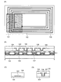
図1に示す半導体装置は、基板100の表面上に第1の絶縁膜103を介してトランジスタ107、第2の絶縁膜104等を有する素子形成層101が設けられ、第2の絶縁膜104上にアンテナとして機能する導電膜102が設けられている。図1では、導電膜102は、少なくとも第2の絶縁膜104および第3の絶縁膜105に接するように設けられている。
In the semiconductor device illustrated in FIG. 1, the
第3の絶縁膜105は、第2の絶縁膜104上に設けられており、断面が凹型形状を有する溝140を有している。溝140は、第3の絶縁膜105を貫通させて第2の絶縁膜104が露出するように設けてもよいし、第3の絶縁膜105を貫通させずに凹ませて設けてもよい。ここでは、第3の絶縁膜105を貫通させて溝140を設けた例を示す。
The third
導電膜102は、溝140によって露出した第2の絶縁膜104の表面と溝140における第3の絶縁膜105の端部を覆うように設けられている。この場合、導電膜102は第3の絶縁膜105の表面の一部と溝140における第3の絶縁膜105の側面に接している。なお、必ずしも第3の絶縁膜の表面に導電膜102が設ける必要はなく、第2の絶縁膜104と溝140における第3の絶縁膜105の側面に接するように設けることも可能である。また、基板の表面に垂直な方向から見た場合に、第3の絶縁膜105に形成された溝140は少なくとも一部がコイル状に形成されている。
The
また、図1では、導電膜102を覆うように保護膜として機能する第4の絶縁膜106が設けられている。この場合、導電膜102の凹みの部分にも第4の絶縁膜106が設けられている。図1(A)は本実施の形態で示す半導体装置の上面図を表し、図1(B)は図1(A)におけるa−b間の断面図を表している。なお、図1においては、説明の都合上、複数のトランジスタ107上にアンテナとして機能する導電膜102を同等の大きさで示しているが、実際には、トランジスタ107と比較して導電膜102の方が各段に大きく設けられている。
In FIG. 1, a fourth
基板100として、バリウムホウケイ酸ガラスや、アルミノホウケイ酸ガラスなどのガラス基板、石英基板、セラミック基板等を用いることができる。また、ステンレスを含む金属基板または半導体基板の表面に絶縁膜を形成したものを用いても良い。他にも、ポリエチレンテレフタレート(PET)、ポリエチレンナフタレート(PEN)、ポリエーテルサルフォン(PES)に代表されるプラスチックや、アクリル等の可撓性を有する合成樹脂からなる基板を用いることも可能である。可撓性を有する基板を用いることによって、半導体装置を曲げることが可能となる。
As the
第1の絶縁膜103として、酸化珪素(SiOx)、窒化珪素(SiNx)、酸化窒化珪素(SiOxNy)(x>y)、窒化酸化珪素(SiNxOy)(x>y)等の酸素または窒素を有する絶縁膜の単層構造、またはこれらの積層構造を用いることができる。また、基板100として可撓性基板等を用いる場合であって、素子形成層101を基板100に貼り合わせて設ける際には、第1の絶縁膜103に酸化珪素、窒化珪素または酸化窒化珪素の他に接着層が含まれていてもよい。接着層としては、アクリル樹脂等を含んだ樹脂材料または合成ゴム材料からなる材料、熱硬化樹脂、紫外線硬化樹脂、エポキシ樹脂系接着剤、光硬化型接着剤、湿気硬化型接着剤、樹脂添加剤等の接着剤が挙げられる。なお、基板100からトランジスタ107等への汚染等の恐れがない場合には、第1の絶縁膜103は必ずしも設ける必要はない。
The first
第2の絶縁膜104、第3の絶縁膜105、第4の絶縁膜106としては、酸化珪素、窒化珪素、酸化窒化珪素、窒化酸化珪素等の酸素または窒素を有する絶縁膜やポリイミド、ポリアミド、ポリビニルフェノール、ベンゾシクロブテン、アクリル、エポキシ等の有機材料、シロキサン系材料等を用いることにより単層又は積層構造として設けることができる。なお、シロキサン系材料とは、シリコンと酸素との結合で骨格構造が構成され、置換基に少なくとも水素を含む物質、又は、シリコンと酸素との結合で骨格構造が構成され、置換基にフッ素、アルキル基、芳香族炭化水素の少なくとも1つを含む物質に相当する。
As the second
素子形成層101は、少なくともトランジスタ107を有している。トランジスタ107としては、例えば、ガラス等の基板上に薄膜トランジスタ(TFT)を形成して設けてもよいし、Si等の半導体基板上に当該基板をチャネルとして電界効果型トランジスタ(FET)を設けてもよいし、可撓性を有する基板上に有機TFTを設けてもよい。また、トランジスタ107によって、CPU、メモリまたはマイクロプロセッサ等のありとあらゆる集積回路を設けることができる。図1では、トランジスタ107として薄膜トランジスタを設けた例を示している。また、トランジスタ107の構造として、nチャネル型半導体とpチャネル型半導体とを組み合わせたCMOSとして設けている。また、半導体膜に不純物領域(ソース領域、ドレイン領域、LDD領域を含む)設け、ゲート電極の側面と接するように絶縁膜(サイドウォール)を設けている。実施の形態1では、nチャネル型の半導体膜にLDDを形成し、pチャネル型の半導体膜にはLDDを設けていない例を示しているが、もちろんpチャネル型の半導体膜にもnチャネル型半導体膜と同様にLDD領域を設けてもよい。また、ソース領域およびドレイン領域とゲート電極の一方または両方に、ニッケル、モリブデンまたはコバルト等のシリサイド層を形成してもよい。
The
導電膜102としては、スパッタ法、CVD法等で形成された銅(Cu)、アルミニウム(Al)や銀(Ag)や金(Au)、クロム(Cr)、モリブデン(Mo)、チタン(Ti)、タンタル(Ta)、タングステン(W)、ニッケル(Ni)、炭素(C)等の金属や金属化合物を1つまたは複数有する導電材料を用いることができる。
As the
図1では、第2の絶縁膜104上に断面が凹型形状の溝140を有する第3の絶縁膜105を形成し、溝140における第2の絶縁膜104の表面と第3の絶縁膜105の側面に沿うように導電膜102を設けている。ここでは、スパッタ法またはCVD法で導電膜を全面に形成した後、フォトリソグラフィ法により選択的にエッチングを行うことにより形成することができる。このように導電膜102を設ける(図1(D))ことにより、平坦な面上に導電膜を断面が矩形状になるように設ける場合(図1(C))と比較して、導電膜102の断面積および表面積を大きくすることができる。つまり、第2の絶縁膜104上に導電膜102を設けた場合(図1(C))は、導電膜102の断面は矩形状となる。一方、第3の絶縁膜105に断面が凹型形状の溝140を設け、当該溝140に沿って導電膜102を形成することによって、導電膜102は断面が凹型形状を有するようになる。そのため、第3の絶縁膜105に設けられた凹型形状の溝140に沿うように導電膜102を設けた場合(図1(D))は、図1(C)と比較して第3の絶縁膜105の側面に接する部分108だけ断面積および表面積が大きくなる。このように、アンテナとして機能する導電膜の断面積および表面積が増加することによって、非接触でデータのやりとりを行う場合に、半導体装置と外部機器(リーダ/ライタ)との通信距離や通信帯域を向上させることが可能となる。また、アンテナとして機能する導電膜と絶縁膜との接触面積が増加することにより密着性の向上を図ることができる。
In FIG. 1, a third
また、図1においては、第2の絶縁膜104上に溝140を有する第3の絶縁膜105を設け、第2の絶縁膜104と第3の絶縁膜105上に選択的に導電膜102を設けているが、本実施の形態で示す半導体装置はこの構造に限られない。他の構造を有する半導体装置の具体例を図2に示す。
In FIG. 1, a third
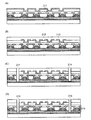
図2(A)に示す半導体装置は、第2の絶縁膜104上に断面が凹型形状の溝を有する第3の絶縁膜105が設けられ、当該溝に沿うように導電膜102が設けられている(領域251)。具体的には、第3の絶縁膜105に設けられた溝は貫通しておらず、導電膜102は、第3の絶縁膜105のみに接触しており、第3の絶縁膜105の凹んだ表面と凹みの端部を覆うように導電膜102が設けられている。第3の絶縁膜105の凹部は、第2の絶縁膜104上に第3の絶縁膜を設けた後に、凹ませる部分を選択的にエッチングすることにより設けることができる。この時エッチング条件を制御することによって任意の形状の凹部を形成することができる。また、他にも第2の絶縁膜104上に第3の絶縁膜105を設けた後に、第3の絶縁膜105および第2の絶縁膜104に凹部を形成し、導電膜102を設ける構成としてもよい(領域252)。
In the semiconductor device illustrated in FIG. 2A, a third
図2(B)に示す半導体装置は、第2の絶縁膜104上に、第3の絶縁膜105の角253を湾曲させることによって、断面がテーパー状の溝を有する第3の絶縁膜105を設け、当該溝における第2の絶縁膜104の表面と第3の絶縁膜105のテーパー部を覆うように導電膜102が設けられている。つまり、図2(B)は図1における第3の絶縁膜105の溝140の断面をテーパー状に設けた場合に相当する。第3の絶縁膜105の溝140の断面をテーパー状に設けることによって、導電膜102を設けた際に深さ方向における導電膜102の段切れを防止することができる。
In the semiconductor device illustrated in FIG. 2B, the third
図2(C)に示す半導体装置は、図1(B)の構造において第2の絶縁膜104上に設ける第3の絶縁膜105に形成される凹部の数を2倍に増やし、導電膜102が凹凸状に設けられている。つまり第3の絶縁膜105の溝140を増やして当該溝に導電膜102を設けることによって、導電膜102の断面積および表面積をより大きくすることができる。また、ここでは凹部の数を2倍としたが、もちろんさらに増やして形成することも可能である。
In the semiconductor device illustrated in FIG. 2C, the number of recesses formed in the third
図2(D)に示す半導体装置は、図2(C)における導電膜102を上下逆に配置した場合を示している。このように、導電膜102を凹凸状に設けることによって、一定の領域における導電膜102の断面積および表面積を大きくすることができる。
The semiconductor device illustrated in FIG. 2D illustrates the case where the
なお、図2(B)〜(D)においても図2(A)と同様に設けることもできる。つまり、図2(B)〜(D)では、第2の絶縁膜104を露出させるように溝を設けているが、第3の絶縁膜105の溝部分を完全に貫通させずに断面が凹型形状の溝を設け、第3の絶縁膜105のみに接触するように導電膜102を設ける構成とすることも可能である。他にも、図2(A)の領域252に示したように、第2の絶縁膜104に断面が凹型形状の溝を設ける構成とすることもできる。
2B to 2D can also be provided similarly to FIG. 2A. That is, in FIGS. 2B to 2D, a groove is provided so as to expose the second
また、図1、図2に示した半導体装置においては、第2の絶縁膜104上に第3の絶縁膜105が設けられているが、第2の絶縁膜104を設けずにトランジスタ107のソースまたはドレイン配線上に第3の絶縁膜105を設けることも可能である。この場合、第3の絶縁膜105に設けられる溝は貫通させて設けてもよいし、貫通させずに設けてもよい。貫通させて設ける場合には、導電膜102をトランジスタ107のソースまたはドレイン配線と同一の層に設けることが可能となる。この場合、導電膜102とソースまたはドレイン配線とを同一の材料で形成することにより工程を簡略化することができる。
In the semiconductor device illustrated in FIGS. 1 and 2, the third
図1では、半導体装置の小型化を図るために、素子形成層101と導電膜102の少なくとも一部が重なるように配置されているが、本実施の形態で示す半導体装置はこの構成に限られず、素子形成層101と導電膜102は重ならないように配置しても良い。また、図1、図2では、電磁結合方式または電磁誘導方式の場合に関して示したが、上述した構成はマイクロ波方式を用いる半導体装置に適用することも可能である。この場合の具体例を図3に示す。
In FIG. 1, in order to reduce the size of the semiconductor device, the
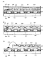
一般的に、電磁結合方式や電磁誘導方式を用いる半導体装置のアンテナはコイル状に設ける必要があるが、マイクロ波方式を用いる半導体装置のアンテナの形状は受信する電磁波に依存する。ここでは、説明を簡単にするために単純な構造であるポール状のアンテナを用いた場合を示す(図3)。 In general, an antenna of a semiconductor device using an electromagnetic coupling method or an electromagnetic induction method needs to be provided in a coil shape, but the shape of the antenna of a semiconductor device using a microwave method depends on received electromagnetic waves. Here, in order to simplify the description, a case where a pole-shaped antenna having a simple structure is used is shown (FIG. 3).
図3(A)において、基板100上に素子形成層111が設けられており、素子形成層111と接続するようにアンテナとして機能する導電膜112a、112bが設けられている。図3(A)におけるa−b間とc−d間の断面構造をそれぞれ図3(B)、(C)に示す。
3A, an
基板100上に第1の絶縁膜103を介してトランジスタ107等を有する素子形成層111が設けられ、素子形成層111の上方に第2の絶縁膜104を介してアンテナとして機能する導電膜112a、112bが設けられている(図3(B)、(C))。導電膜112a、112bは、第2の絶縁膜104上に選択的に設けられた第3の絶縁膜105の端部を覆うように第2の絶縁膜104上および第3の絶縁膜105上に設けられており、素子形成層111のいずれかのトランジスタと電気的に接続している。ここでは、第3の絶縁膜105は開口部を有しており、導電膜112a、112bが第3の絶縁膜の側面と接するように設けられている。また、導電膜112a、112bを覆うように第4の絶縁膜106が設けられている。
An
アンテナとして機能する導電膜112a、112bは、第2の絶縁膜104上および第3の絶縁膜105の端部を覆うように設けられている。また、導電膜112a、112bは、上述した導電膜102と同一の方法や材料を用いて形成することができる。
The
また、上記図1〜3において、アンテナとして機能する導電膜102、またはアンテナとして機能する導電膜112aおよび112bの断面積を増やしたい場合には、導電膜102の凹部に選択的に導電体を設けることが好ましい。例えば、図16(A)に示すように、液滴吐出法を用いてノズル145から導電性を有する組成物146を選択的に導電膜102の凹部に設けることによって断面積を増やすことができる。導電性を有する組成物146としては、Ag、Au、Cu、Pdなどの金属、金属化合物を1つまたは複数有する導電材料を用いる。なお、分散剤により凝集を抑え、溶液に分散させることができるならば、Cr、Mo、Ti、Ta、W、Alなどの金属、金属化合物を1つまたは複数有する導電材料を用いることも可能である。また、他にも、スクリーン印刷法やディスペンサー法を用いて選択的に導電性を有する組成物146を導電膜102の凹部に形成してもよい。その結果、アンテナとして機能する導電膜の断面積は導電膜102と導電体147を合わせたものとなるため、断面積を増加することができる(図16(B))。この場合、第2の絶縁膜104上に形成される導電膜と第3の絶縁膜105上に形成される導電膜の厚さが異なっている。
In FIGS. 1 to 3, in order to increase the cross-sectional area of the
以上のように、アンテナとして機能する導電膜の断面積および表面積を増やすように半導体装置を設けることによって、当該半導体装置の通信距離や通信帯域を向上させることが可能となる。また、アンテナとして機能する導電膜と絶縁膜との接触面積が増加することにより密着性の向上を図ることができる。 As described above, by providing a semiconductor device so as to increase the cross-sectional area and surface area of the conductive film functioning as an antenna, the communication distance and communication band of the semiconductor device can be improved. Further, adhesion can be improved by increasing the contact area between the conductive film functioning as an antenna and the insulating film.
(実施の形態2)
本実施の形態では、上記実施の形態で示した半導体装置の作製方法の一例を図面を用いて説明する。本実施の形態では、素子形成層およびアンテナを一旦ガラス等の剛性を有する基板上に設けた後に、剛性を有する基板から素子形成層やアンテナを剥離し、可撓性を有する基板上に設ける場合に関して示す。
(Embodiment 2)
In this embodiment, an example of a method for manufacturing the semiconductor device described in the above embodiment will be described with reference to drawings. In this embodiment, after the element formation layer and the antenna are once provided over a rigid substrate such as glass, the element formation layer and the antenna are peeled from the rigid substrate and provided over the flexible substrate. To show.
まず、基板200上に下地となる絶縁膜201を形成し、その上に剥離層202を設け、剥離層202上に絶縁膜203、半導体膜204を積層して設ける(図4(A))。下地となる絶縁膜201は、基板200から剥離層202への汚染を防止するために設けているが、基板200からの汚染等の恐れがない場合には絶縁膜201を必ずしも設ける必要はない。また、ここでは絶縁膜201、剥離層202、絶縁膜203および半導体膜204を真空工程で行う場合に連続して成膜することが可能である。
First, the
次に、半導体膜204を選択的にエッチングすることによって島状の半導体膜を複数設け、当該島状の半導体膜上にゲート絶縁膜を介してゲート電極を形成することによって薄膜トランジスタ205を複数設ける(図4(B))。
Next, a plurality of island-shaped semiconductor films are provided by selectively etching the
次に、薄膜トランジスタ205を覆うように絶縁膜206を形成し、さらに平坦化を図るために絶縁膜207を形成する。次に、絶縁膜206、絶縁膜207に選択的に開口部を設け、薄膜トランジスタ205のソース領域およびドレイン領域と電気的に接続するように導電膜208を設け、その後、導電膜208を覆うように絶縁膜209を形成する(図4(C))。
Next, an insulating
次に、絶縁膜209上に選択的に絶縁膜210を設ける(図4(D))。絶縁膜210は、溝218を有しており、絶縁膜209上の全面に絶縁膜210を形成した後にフォトリソグラフィ法により溝218を形成してもよいし、絶縁膜209上にスクリーン印刷等の印刷法や液滴吐出法を用いることによって選択的に絶縁膜210を形成することによって溝218を設けてもよい。印刷法や液滴吐出法等を用いることによって作製工程を減らすことができる。なお、絶縁膜210の溝218は、上記実施の形態で示したいずれかの構造を用いることが可能である。
Next, the insulating
次に、絶縁膜209および絶縁膜210を覆うように導電膜211を形成する(図5(A))。ここでは、導電膜211は、絶縁膜210が有する溝218によって露出している絶縁膜209の表面と絶縁膜210の側面および表面に接して設けられている。なお、導電膜211の溝218における段切れを防止するために、絶縁膜210の角を湾曲するように形成することにより溝218をテーパー状に設けることが好ましい。
Next, a
次に、導電膜211を選択的にエッチングすることにより導電膜212を形成し、その後、導電膜212を覆うように絶縁膜213を形成する(図5(B))。
Next, the
次に、選択的に絶縁膜203、206、207、209、210、213を除去することにより、剥離層202を露出させるように開口部214を形成する(図5(D))。なお、開口部214は、薄膜トランジスタ205を避けた領域に設けるようにする。開口部214は、レーザ光の照射やフォトリソグラフィ法により形成することができる。
Next, by selectively removing the insulating
次に、開口部214からエッチング剤215を導入することによって剥離層202を除去する(図5(D))。剥離層202は全て除去してもよいし、エッチングの条件を制御することによって剥離層202の一部を残すように除去してもよい。剥離層202の一部を残すことによって、剥離層202を除去した後も素子形成層219等が基板200から完全に剥離せずにバラバラになることを防ぐことができる。さらに、エッチング時間の短縮やエッチング剤の低減させることができるため作業効率の向上および低コスト化を図ることができる。
Next, the
次に、絶縁膜213に粘着性を有する基板216を貼り合わせて設け、素子形成層219を基板200から剥離させる(図6(A))。ここでは、基板200と素子形成層219における絶縁膜203とが、一部残存した剥離層によってつながっているため、物理的手段を用いて基板200から素子形成層219等を剥離させる。
Next, an
なお、ここでは、エッチング剤215を用いて剥離層202を除去する例を示したが、必ずしも剥離層202をエッチング剤により除去する必要はない。つまり、開口部214を形成後に素子形成層219と剥離層202との密着性が十分でない場合には、物理的手段を用いて基板200から素子形成層219を剥離することができる。この場合、エッチング剤を用いる必要がないため、工程の短縮化やコストを低減することが可能となる。
Note that although the example in which the
次に、絶縁膜203の表面に可撓性を有する基板217を貼り合わせて設ける(図6(B))。
Next, a
以上の工程によって、可撓性を有する基板上に素子形成層やアンテナ等を有する半導体装置を設けることができる。以下に、上記工程において用いる材料等の具体的な説明を行う。 Through the above steps, a semiconductor device including an element formation layer, an antenna, and the like can be provided over a flexible substrate. Below, the material etc. which are used in the said process are demonstrated concretely.
基板200としては、ガラス基板、石英基板、金属基板やステンレス基板の一表面に絶縁膜を形成したもの等を用いることができる。このような基板であれば、その面積や形状に大きな制限はないため、基板200として、例えば、1辺が1メートル以上であって、矩形状のものを用いれば、生産性を格段に向上させることができる。このような利点は、円形のシリコン基板を用いる場合と比較すると、大きな優位点である。また、本実施の形態では、剥離された基板200は再利用することができため、より低コストで半導体装置を作製することができる。例えば、原価の高い石英基板を用いた場合であっても、繰り返し石英基板を利用することにより、低コストで半導体装置を作製することができるといった利点を有している。
As the
絶縁膜201としては、酸化珪素(SiOx)、窒化珪素(SiNx)、酸化窒化珪素(SiOxNy)(x>y)、窒化酸化珪素(SiNxOy)(x>y)等の酸素または窒素を有する絶縁膜の単層構造、またはこれらの積層構造を用いることができる。これらの絶縁膜は、公知の手段(スパッタ法やプラズマCVD法等の各種CVD法)を用いて形成することができる。
As the insulating
剥離層202としては、金属膜や金属膜と金属酸化膜の積層構造等を用いることができる。金属膜としては、タングステン(W)、モリブデン(Mo)、チタン(Ti)、タンタル(Ta)、ニオブ(Nb)、ニッケル(Ni)、コバルト(Co)、ジルコニウム(Zr)、亜鉛(Zn)、ルテニウム(Ru)、ロジウム(Rh)、パラジウム(Pd)、オスミウム(Os)、イリジウム(Ir)から選択された元素または前記元素を主成分とする合金材料若しくは化合物材料からなる膜を単層又は積層して形成する。また、これらの材料は、スパッタ法やプラズマCVD法等の各種CVD法等を用いて形成することができる。金属膜と金属酸化膜の積層構造としては、上述した金属膜を形成した後に、酸素雰囲気下またはN2O雰囲気下におけるプラズマ処理、酸素雰囲気下またはN2O雰囲気下における加熱処理を行うことによって、金属膜表面に当該金属膜の酸化物または酸化窒化物を設けることができる。例えば、金属膜としてスパッタ法やCVD法等によりタングステン膜を設けた場合、タングステン膜にプラズマ処理を行うことによって、タングステン膜表面にタングステン酸化物からなる金属酸化膜を形成することができる。また、この場合、タングステンの酸化物は、WOxで表され、xは2〜3であり、xが2の場合(WO2)、xが2.5の場合(W2O5)、xが2.75の場合(W4O11)、xが3の場合(WO3)などがある。タングステンの酸化物を形成するにあたり、上記に挙げたxの値に特に制約はなく、エッチングレート等を基に、どの酸化物を形成するかを決めるとよい。他にも、例えば、金属膜(例えば、タングステン)を形成した後に、当該金属膜上にスパッタ法で酸化珪素(SiO2)等の絶縁膜を設けると共に、金属膜上に金属酸化物(例えば、タングステン上にタングステン酸化物)を形成してもよい。また、プラズマ処理として、例えば上述した高密度プラズマ処理を行ってもよい。また、金属酸化膜の他にも、金属窒化物や金属酸化窒化物を用いてもよい。この場合、金属膜に窒素雰囲気下または窒素と酸素雰囲気下でプラズマ処理や加熱処理を行えばよい。
As the
絶縁膜203としては、公知の手段(スパッタ法やプラズマCVD法等)により、酸化珪素(SiOx)、窒化珪素(SiNx)、酸化窒化珪素(SiOxNy)(x>y)、窒化酸化珪素(SiNxOy)(x>y)等の酸素または窒素を有する絶縁膜の単層構造、またはこれらの積層構造を用いて形成することができる。例えば、絶縁膜203を2層構造で設ける場合、1層目の絶縁膜として窒化酸化珪素膜を形成し、2層目の絶縁膜として酸化窒化珪素膜を形成するとよい。また、絶縁膜203を3層構造で設ける場合、1層目の絶縁膜として酸化窒化珪素膜を形成し、2層目の絶縁膜として窒化酸化珪素膜を形成し、3層目の絶縁膜として酸化窒化珪素膜を形成するとよい。
As the insulating
半導体膜204としては、非晶質半導体、非晶質状態と結晶状態とが混在したSAS、非晶質半導体中に0.5nm〜20nmの結晶粒を観察することができる微結晶半導体、及び結晶性半導体のいずれかの状態で設けることができる。また、基板200として、成膜処理温度に耐えうる基板、例えば石英基板を使用するならば、当該基板へCVD法等により結晶性半導体膜を形成してもよい。また、結晶性半導体膜は、非晶質半導体膜を形成し、加熱処理により結晶化することによって形成することができる。なお、加熱処理とは、加熱炉、レーザ照射、もしくはレーザ光の代わりにランプから発する光の照射(ランプアニール)、またはそれらを組み合わせて用いることができる。レーザ照射を用いる場合、連続発振型のレーザ(CWレーザー)やパルス発振型のレーザ(パルスレーザ)を用いることができる。レーザとしては、Arレーザ、Krレーザ、エキシマレーザ、YAGレーザ、Y2O3レーザ、YVO4レーザ、YLFレーザ、YAlO3レーザ、ガラスレーザ、ルビーレーザ、アレキサンドライトレーザ、Ti:サファイアレーザ、銅蒸気レーザまたは金蒸気レーザのうち一種または複数種を用いることができる。このようなレーザの基本波、及び当該基本波の第2高調波から第4高調波のレーザを照射することで、大粒径の結晶を得ることができる。
As the
薄膜トランジスタ205としては、どのような構造としてもよく、例えば不純物領域(ソース領域、ドレイン領域、LDD領域を含む)を形成してもよいし、pチャネル型、nチャネル型またはpチャネル型とnチャネル型の半導体を組み合わせたCMOS回路で設けてもよい。また、半導体膜の上方に設けられるゲート電極の側面と接するように絶縁膜(サイドウォール)を形成してもよいし、ソース領域およびドレイン領域とゲート電極の一方または両方に、ニッケル、モリブデンまたはコバルト等のシリサイド層を形成してもよい。
The
絶縁膜206としては、公知の手段(スパッタ法やプラズマCVD法等)により、酸化珪素(SiOx)、窒化珪素(SiNx)、酸化窒化珪素(SiOxNy)(x>y)、窒化酸化珪素(SiNxOy)(x>y)等の酸素または窒素を有する絶縁膜やDLC(ダイヤモンドライクカーボン)等の炭素を含む膜の単層構造、またはこれらの積層構造を用いて形成することができる。
As the insulating
絶縁膜207、209、210、213としては、上記酸化珪素(SiOx)、窒化珪素(SiNx)、酸化窒化珪素(SiOxNy)(x>y)、窒化酸化珪素(SiNxOy)(x>y)等の酸素または窒素を有する絶縁膜やDLC(ダイヤモンドライクカーボン)等の炭素を含む膜はもちろん、その他にもエポキシ、ポリイミド、ポリアミド、ポリビニルフェノール、ベンゾシクロブテン、アクリル等の有機材料、シロキサン系材料等の単層または積層構造を用いて形成することができる。特にエポキシ、ポリイミド、ポリアミド、ポリビニルフェノール、ベンゾシクロブテン、アクリル等の有機材料、シロキサン系材料等の材料は、スピンコーティング法、液滴吐出法または印刷法等を用いることによって形成することができるため、平坦化や処理時間の効率化を図ることができる。絶縁膜207、209、210、213は、全て同じ材料を用いて形成してもよいし、別々の材料を用いて形成してもよい。
As the insulating
導電膜208としては、Al、Ni、C、W、Mo、Ti、Pt、Cu、Ta、Au、Mnから選ばれた一種の元素または当該元素を複数含む合金からなる単層または積層構造を用いることができる。例えば、当該元素を複数含む合金からなる導電膜として、例えばCとTiを含有したAl合金(Al−Ti−C)、Niを含有したAl合金(Al−Ni)、CとNiを含有したAl合金(Al−Ni−C)、CとMnを含有したAl合金(Al−Mn−C)等を用いることができる。
As the
導電膜211としては、スパッタ法やCVD法等により形成した銅(Cu)、アルミニウム(Al)や銀(Ag)や金(Au)、クロム(Cr)、モリブデン(Mo)、チタン(Ti)、タンタル(Ta)、タングステン(W)、ニッケル(Ni)、炭素(C)等の金属や金属化合物を1つまたは複数有する導電材料を用いることができる。また、他にも、スクリーン印刷法を用いて導電性を有するペースト(例えば、銀ペースト)を選択的に形成することもできる。
As the
基板216としては、ラミネートフィルムを用いることができる。ここでは、ポリエステル等のフィルム上にホットメルトフィルムが形成されたものを利用することができる。また、基板216に絶縁膜213に接着させる際に、加圧処理または加熱処理の一方または両方を行うことによって、効率的に接着することができる。また、封止後にフィルムを通して素子形成層219に水分等が入り込まないように、あらかじめ基板216に、酸化珪素(SiOx)、窒化珪素(SiNx)、酸化窒化珪素(SiOxNy)(x>y)、窒化酸化珪素(SiNxOy)(x>y)の膜をコートしておくと好ましい。
As the
また、基板216として、静電気等を防止する帯電防止対策を施したフィルム(以下、帯電防止フィルムと記す)を用いることもできる。帯電防止フィルムとしては、帯電防止可能な材料を樹脂中に分散させたフィルム、及び帯電防止可能な材料が貼り付けられたフィルム等が挙げられる。帯電防止可能な材料が設けられたフィルムは、片面に帯電防止可能な材料を設けたフィルムであってもよいし、両面に帯電防止可能な材料を設けたフィルムであってもよい。さらに、片面に帯電防止可能な材料が設けられたフィルムは、帯電防止可能な材料が設けられた面をフィルムの内側になるように層に貼り付けてもよいし、フィルムの外側になるように貼り付けてもよい。なお、帯電防止可能な材料はフィルムの全面、あるいは一部に設けてあればよい。ここでの帯電防止可能な材料としては、金属、インジウムと錫の酸化物(ITO)、両性界面活性剤や陽イオン性界面活性剤や非イオン性界面活性剤等の界面活性剤を用いることができる。また、他にも帯電防止材料として、側鎖にカルボキシル基および4級アンモニウム塩基をもつ架橋性共重合体高分子を含む樹脂材料等を用いることができる。これらの材料をフィルムに貼り付けたり、練り込んだり、塗布したりすることによって帯電防止フィルムとすることができる。帯電防止フィルムで封止を行うことによって、商品として取り扱う際に、外部からの静電気等によって半導体素子に悪影響が及ぶことを抑制することができる。
Further, as the
なお、本実施の形態では、コイル状のアンテナを有する半導体装置を作製する場合に関して示したが、もちろんその他の形状のアンテナを有する半導体装置を作製する場合も同様に行うことができる。 Note that although the case where a semiconductor device having a coiled antenna is manufactured has been described in this embodiment mode, it is needless to say that semiconductor devices having antennas having other shapes can be manufactured in the same manner.
本実施の形態は、上記実施の形態と自由に組み合わせて行うことができる。 This embodiment can be freely combined with the above embodiment.
(実施の形態3)
本実施の形態では、上記実施の形態と異なる半導体装置およびその作製方法に関して図面を用いて説明する。具体的には、素子形成層とアンテナを別途作製し、素子形成層とアンテナとを接続して設ける場合に関して説明する。なお、本実施の形態では、コイル状のアンテナを適用した場合に関して説明を行うが、その他の形状のアンテナを適用する場合であっても同様に行うことができる。
(Embodiment 3)
In this embodiment, a semiconductor device and a manufacturing method thereof which are different from those in the above embodiment will be described with reference to drawings. Specifically, a case where an element formation layer and an antenna are separately manufactured and the element formation layer and the antenna are connected to each other will be described. Note that although a case where a coiled antenna is applied is described in this embodiment mode, the present invention can be similarly performed even when antennas of other shapes are applied.
素子形成層は、上記図4に示した作製方法を用いることによって形成することができる。ここではアンテナの作製方法に関して以下に図面を用いて説明する。 The element formation layer can be formed by using the manufacturing method shown in FIG. Here, a method for manufacturing an antenna will be described with reference to the drawings.
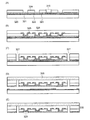
まず、基板310上に溝315を有する絶縁膜311を選択的に形成する(図9(A))。絶縁膜311の溝は、基板310上の全面に絶縁膜311を設けた後にフォトリソグラフィ法を用いて形成してもよいし、スクリーン印刷等の印刷法や液滴吐出法を用いて基板310上に選択的に絶縁膜311を設けることによって形成してもよい。
First, an insulating
次に、溝315における基板310の表面および絶縁膜311を覆うように導電膜312を形成する(図9(B))。導電膜312は、CVD法、スパッタ法、スクリーン印刷法等であって、めっき法以外であればどのような方法で設けてもよい。
Next, a
次に、導電膜312をエッチング法等を用いて選択的に除去することにより導電膜316を設け、当該導電膜316を覆うように絶縁膜313を設ける(図9(C))。導電膜316は、絶縁膜311上に設けられた導電膜312の一部を除去し、溝315内および絶縁膜311の端部を覆うように形成する。
Next, the
次に、絶縁膜313に開口部314を設ける(図9(D))。開口部314は、フォトリソグラフィ法やレーザ光を照射することによって設ける。なお、絶縁膜313を設ける際にスクリーン印刷等の印刷法や液滴吐出法を用いて、開口部314となる領域以外に選択的に絶縁膜313を形成することによって開口部314を設けてもよい。
Next, an
以上の工程により、アンテナ形成層317を得ることができる。次に、素子形成層とアンテナ形成層を貼り合わせて設けた場合に関して図7に示す。図7(A)〜(C)は、別々に形成した素子形成層101とアンテナ形成層317とを電気的に接続する場合の構成例を示している。
Through the above steps, the
図7(A)に示す半導体装置は、図9で示したアンテナ形成層317と素子形成層101とが接着性を有する樹脂305によって貼り合わされることによって設けられている。そして、トランジスタ107のソースまたはドレイン領域に電気的に接続された導電膜304とアンテナとして機能する導電膜312とが接続領域307において、樹脂305中に含まれる導電性微粒子306を介して電気的に接続されている。ここでは、導電性微粒子を用いて素子形成層とアンテナ形成層を電気的に接続した例を示しているが、銀ペースト、銅ペーストまたはカーボンペースト等の導電性接着剤や半田接合等を用いて接続することも可能である。
The semiconductor device illustrated in FIG. 7A is provided by bonding the
図7(B)に示す半導体装置は、図9において凹型に設けた導電膜316を凸型に設けた場合を示している。接続領域307において、導電膜316の凸型の表面と導電膜304とが導電性微粒子306を介して電気的に接続されている。なお、接続領域307に配置される導電膜316の凸部を接続領域以外に配置される導電膜316の凸部より高く設けることによって、導電膜304との間隔を小さくすることができるため導電性微粒子306を用いる場合の接続をより確実なものとすることができる。この場合、アンテナ形成層の作製時に接続領域307に配置される導電膜316の下方に位置する絶縁膜311を他の絶縁膜311より厚く形成しておけばよい。
The semiconductor device illustrated in FIG. 7B illustrates the case where the
図7(C)に示す半導体装置は、配線318を用いたワイヤーボンディング法によってアンテナ形成層317と素子形成層101とが電気的に接続されて設けられている。この場合、アンテナ形成層317は図7(C)に示すように素子形成層101上に接着剤等を用いて貼り合わせて設けてもよいし、他にも素子形成層101と同一平面や下方に設けることも可能である。
In the semiconductor device illustrated in FIG. 7C, the
本実施の形態は、上記実施の形態と自由に組み合わせて行うことができる。 This embodiment can be freely combined with the above embodiment.
(実施の形態4)
本実施の形態では、上記実施の形態と異なる半導体装置に関して図面を用いて説明する。具体的には、素子形成層とアンテナ形成層を別途作製し、素子形成層とアンテナ形成層とを接続して設ける場合に関して上記実施の形態3とは異なる場合に関して説明する。なお、本実施の形態では、コイル状のアンテナを適用した場合に関して説明を行うが、その他の形状のアンテナを適用する場合であっても同様に行うことができる。
(Embodiment 4)
In this embodiment, a semiconductor device different from the above embodiment will be described with reference to drawings. Specifically, a case in which an element formation layer and an antenna formation layer are separately formed and the element formation layer and the antenna formation layer are connected and provided is different from that in Embodiment Mode 3. Note that although a case where a coiled antenna is applied is described in this embodiment mode, the present invention can be similarly performed even when antennas of other shapes are applied.
素子形成層は、上記図4に示した作製方法を用いることによって形成することができる。アンテナ形成層の作製方法に関して図10を用いて以下に説明する。 The element formation layer can be formed by using the manufacturing method shown in FIG. A method for manufacturing the antenna formation layer will be described below with reference to FIGS.
まず、基板320上に下地膜として機能する絶縁膜321、剥離層322および絶縁膜323を積層して設け、絶縁膜323上に溝315を有する絶縁膜324を設ける(図10(A))。
First, the insulating
次に、図5(A)〜(C)に示した方法を用いて、導電膜325および当該導電膜325を覆うように絶縁膜326を形成する(図10(B))。
Next, using the method illustrated in FIGS. 5A to 5C, the
次に、絶縁膜323、324、326を選択的に除去して剥離層322を露出させて開口部327を形成し、開口部327にエッチング剤を導入することによって剥離層322を除去する(図10(C))。
Next, the insulating
次に、絶縁膜326の表面に可撓性を有する基板328を貼り合わせ、絶縁膜323から基板320を剥離する(図10(D))。
Next, a
次に、選択的に絶縁膜323の一部分をレーザ光の照射やエッチング法を用いて除去し、開口部329を設けることによって、導電膜325を露出させる(図10(E))。
Next, part of the insulating
以上の工程により、アンテナ形成層を形成することができる。なお、図10の作製方法は図4〜図6に示した作製方法において、素子形成層の代わりに剥離層の上にアンテナ形成層を設けている。そのため、図10において図4〜図6に示した材料等を適用することができる。 Through the above steps, the antenna formation layer can be formed. Note that the manufacturing method in FIG. 10 is the same as the manufacturing method shown in FIGS. 4 to 6 except that an antenna formation layer is provided over the separation layer instead of the element formation layer. Therefore, the materials shown in FIGS. 4 to 6 in FIG. 10 can be applied.
次に、素子形成層とアンテナ形成層を貼り合わせて設ける場合に関して図8に示す。図8(A)〜(C)は、別々に形成した素子形成層101とアンテナ形成層330とを電気的に接続する場合の構成例を示している。
Next, FIG. 8 illustrates the case where an element formation layer and an antenna formation layer are provided to be bonded to each other. 8A to 8C illustrate a configuration example in the case where the
図8(A)に示す半導体装置は、図10で示したアンテナ形成層330と素子形成層101とが接着性を有する樹脂305によって貼り合わされることによって設けられている。トランジスタ107のソースまたはドレイン領域に電気的に接続された導電膜304とアンテナとして機能する導電膜325とが接続領域307において、樹脂305中に含まれる導電性微粒子306を介して電気的に接続されている。ここでは、導電性微粒子を用いて素子形成層とアンテナ形成層を電気的に接続した例を示しているが、銀ペースト、銅ペーストまたはカーボンペースト等の導電性接着剤や半田接合を用いて接続することも可能である。
The semiconductor device illustrated in FIG. 8A is provided by bonding the
図8(B)に示す半導体装置は、図10において凹型に設けた導電膜316を凸型に設けた場合を示している。接続領域307において、導電膜325の凸型の表面と導電膜304とが導電性微粒子306を介して電気的に接続されている。
The semiconductor device illustrated in FIG. 8B illustrates the case where the
図8(C)に示す半導体装置は、配線318を用いたワイヤーボンディング法によってアンテナ形成層317と素子形成層101とが電気的に接続されて設けられている。この場合、アンテナ形成層317は図7(C)に示すように素子形成層101上に接着剤等を用いて貼り合わせて設けてもよいし、他にも素子形成層101と同一平面や下方に設けることも可能である。
In the semiconductor device illustrated in FIG. 8C, the
本実施の形態で示した方法は、特にアンテナとして機能する導電膜325の形成時の温度が高温で可撓性を有する基板上に直接導電膜325を設けることが困難である場合に有効となる。つまり、一度作製工程の処理温度に耐えることが可能な基板に剥離層を介してアンテナ形成層を設けた後に、基板からアンテナ形成層を剥離することによって、可撓性を有する基板上にアンテナ形成層を設けることができる。
The method described in this embodiment mode is particularly effective when the
本実施の形態は、上記実施の形態と自由に組み合わせて行うことができる。 This embodiment can be freely combined with the above embodiment.
(実施の形態5)
本実施の形態では、本発明の半導体装置の作製方法の一例について、図面を参照して説明する。具体的には、素子形成層におけるトランジスタとして薄膜トランジスタ(TFT)を用い、支持基板上にTFTを含む素子形成層を設けた後に支持基板から素子形成層を分離する剥離法により半導体装置を作製する例を示す。
(Embodiment 5)
In this embodiment, an example of a method for manufacturing a semiconductor device of the present invention will be described with reference to drawings. Specifically, an example in which a thin film transistor (TFT) is used as a transistor in an element formation layer and a semiconductor device is manufactured by a separation method in which an element formation layer including a TFT is provided over a support substrate and then the element formation layer is separated from the support substrate. Indicates.
まず、基板701の一表面に、剥離層702を形成する(図11(A))。基板701は、ガラス基板、石英基板、金属基板やステンレス基板の一表面に絶縁膜を形成したもの、本工程の処理温度に耐えうる耐熱性があるプラスチック基板等を用いるとよい。このような基板701であれば、その面積や形状に大きな制限はないため、基板701として、例えば、1辺が1メートル以上であって、矩形状のものを用いれば、生産性を格段に向上させることができる。このような利点は、円形のシリコン基板を用いる場合と比較すると、大きな優位点である。なお、本工程では、剥離層702は、基板701の全面に設けているが、必要に応じて、基板701の全面に剥離層を設けた後に、フォトリソグラフィ法により選択的にエッチングして設けてもよい。また、基板701に接するように剥離層702を形成しているが、必要に応じて、基板701に接するように下地となる絶縁膜を形成し、当該絶縁膜に接するように剥離層702を形成してもよい。
First, the
剥離層702は、金属膜と当該金属酸化膜により形成されている。金属膜は、公知の手段(スパッタリング法やプラズマCVD法等)により、タングステン(W)、モリブデン(Mo)、チタン(Ti)、タンタル(Ta)、ニオブ(Nd)、ニッケル(Ni)、コバルト(Co)、ジルコニウム(Zr)、亜鉛(Zn)、ルテニウム(Ru)、ロジウム(Rh)、鉛(Pd)、オスミウム(Os)、イリジウム(Ir)から選択された元素または前記元素を主成分とする合金材料若しくは化合物材料からなる層を、単層又は積層して形成する。金属酸化膜は、金属膜に酸素雰囲気下でプラズマ処理を行うか、金属膜に酸素雰囲気下で熱処理を行うことによって金属膜の表面に形成する。なお、金属酸化膜の他にも金属酸化窒化物を用いてもよい。
The
金属膜が単層構造の場合、例えば、タングステン層、モリブデン層またはタングステンとモリブデンの混合物を含む層を形成する。そして、金属膜の表面に、タングステンの酸化物若しくは酸化窒化物を含む層、モリブデンの酸化物若しくは酸化窒化物を含む層またはタングステンとモリブデンの混合物の酸化物若しくは酸化窒化物を含む層を形成する。なお、タングステンとモリブデンの混合物とは、例えば、タングステンとモリブデンの合金に相当する。 In the case where the metal film has a single-layer structure, for example, a tungsten layer, a molybdenum layer, or a layer containing a mixture of tungsten and molybdenum is formed. Then, a layer containing tungsten oxide or oxynitride, a layer containing molybdenum oxide or oxynitride, or a layer containing oxide or oxynitride of a mixture of tungsten and molybdenum is formed on the surface of the metal film. . Note that the mixture of tungsten and molybdenum corresponds to, for example, an alloy of tungsten and molybdenum.
また、剥離層702として、基板701上に金属膜を形成した後に、酸素雰囲気下で上記金属膜の材料をターゲットとして、スパッタ法により金属酸化膜を形成してもよい。この場合、金属膜と金属酸化膜を別の金属元素を用いて形成することもできる。なお、基板701上に、直接金属酸化膜を形成しこれを剥離層702として用いてもよい。
Alternatively, after forming a metal film over the
次に、剥離層702を覆うように、下地となる絶縁膜703を形成する。絶縁膜703は、公知の手段(スパッタ法やプラズマCVD法等)により、珪素の酸化物または珪素の窒化物を含む膜を、単層又は積層で形成する。下地となる絶縁膜が2層構造の場合、例えば、1層目として窒化酸化珪素膜を形成し、2層目として酸化窒化珪素膜を形成するとよい。下地となる絶縁膜が3層構造の場合、1層目の絶縁膜として酸化珪素膜を形成し、2層目の絶縁膜として窒化酸化珪素膜を形成し、3層目の絶縁膜として酸化窒化珪素膜を形成するとよい。または、1層目の絶縁膜として酸化窒化珪素膜を形成し、2層目の絶縁膜として窒化酸化珪素膜を形成し、3層目の絶縁膜として酸化窒化珪素膜を形成するとよい。下地となる絶縁膜は、基板701からの不純物の侵入を防止するブロッキング膜として機能する。
Next, an insulating
次に、絶縁膜703上に、非晶質半導体膜704(例えば非晶質珪素を含む膜)を形成する。非晶質半導体膜704は、公知の手段(スパッタ法、LPCVD法、プラズマCVD法等)により、25〜200nm(好ましくは30〜150nm)の厚さで形成する。続いて、非晶質半導体膜704を公知の結晶化法(レーザ結晶化法、RTA又はファーネスアニール炉を用いる熱結晶化法、結晶化を助長する金属元素を用いる熱結晶化法、結晶化を助長する金属元素を用いる熱結晶化法とレーザ結晶化法を組み合わせた方法等)により結晶化して、結晶質半導体膜を形成する。その後、得られた結晶質半導体膜を所望の形状にエッチングして、結晶質半導体膜706〜710を形成する(図11(B))。なお、剥離層702、絶縁膜703および非晶質半導体膜704は、連続して形成することができる。
Next, an amorphous semiconductor film 704 (eg, a film containing amorphous silicon) is formed over the insulating
結晶質半導体膜706〜710の作製工程の一例を以下に簡単に説明すると、まず、プラズマCVD法を用いて、膜厚66nmの非晶質半導体膜を形成する。次に、結晶化を助長する金属元素であるニッケルを含む溶液を非晶質半導体膜上に保持させた後、非晶質半導体膜に脱水素化の処理(500℃、1時間)と、熱結晶化の処理(550℃、4時間)を行って結晶質半導体膜を形成する。その後、必要に応じてレーザ光を照射し、フォトリソグラフィ法を用いることによって結晶質半導体膜706〜710を形成する。
An example of a manufacturing process of the
レーザ結晶化法で結晶質半導体膜を形成する場合、連続発振またはパルス発振の気体レーザ又は固体レーザを用いる。気体レーザとしては、エキシマレーザ、YAGレーザ、YVO4レーザ、YLFレーザ、YAlO3レーザ、ガラスレーザ、ルビーレーザ、Ti:サファイアレーザ等を用いる。固体レーザとしては、Cr、Nd、Er、Ho、Ce、Co、Ti又はTmがドーピングされたYAG、YVO4、YLF、YAlO3などの結晶を使ったレーザを用いる。特に、連続発振のレーザの基本波、及び当該基本波の第2高調波から第4高調波のレーザを照射することで、大粒径の結晶を得ることができる。例えば、Nd:YVO4レーザ(基本波1064nm)の第2高調波(532nm)や第3高調波(355nm)を用いることができる。なお連続発振の基本波のレーザ光と連続発振の高調波のレーザ光とを照射するようにしてもよいし、連続発振の基本波のレーザ光とパルス発振の高調波のレーザ光とを照射するようにしてもよい。複数のレーザ光を照射することにより、エネルギーを補うことができる。またパルス発振型のレーザであって、半導体膜がレーザ光によって溶融してから固化するまでに、次のパルスのレーザ光を照射できるような発振周波数でレーザ光を発振させることで、走査方向に向かって連続的に成長した結晶粒を得ることができる。すなわち、パルス発振の周期が、半導体膜が溶融してから完全に固化するまでの時間よりも短くなるように、発振の周波数の下限を定めたパルス発振のレーザを使用することができる。このようなレーザとして、発振周波数が10MHz以上のパルス発振のレーザ光を用いてもよい。 In the case of forming a crystalline semiconductor film by a laser crystallization method, a continuous wave or pulsed gas laser or solid state laser is used. As the gas laser, excimer laser, YAG laser, YVO 4 laser, YLF laser, YAlO 3 laser, glass laser, ruby laser, Ti: sapphire laser, or the like is used. As the solid-state laser, a laser using a crystal such as YAG, YVO 4 , YLF, or YAlO 3 doped with Cr, Nd, Er, Ho, Ce, Co, Ti, or Tm is used. In particular, a crystal having a large grain size can be obtained by irradiating a fundamental wave of a continuous wave laser and a second to fourth harmonic laser of the fundamental wave. For example, a second harmonic (532 nm) or a third harmonic (355 nm) of an Nd: YVO 4 laser (fundamental wave 1064 nm) can be used. The continuous wave fundamental laser beam and the continuous wave harmonic laser beam may be irradiated, or the continuous wave fundamental laser beam and the pulsed harmonic laser beam may be irradiated. You may do it. By irradiating a plurality of laser beams, energy can be supplemented. Also, it is a pulse oscillation type laser that oscillates the laser light at an oscillation frequency that can be irradiated with the laser light of the next pulse after the semiconductor film is melted by the laser light and solidifies in the scanning direction. Crystal grains grown continuously can be obtained. That is, it is possible to use a pulsed laser in which the lower limit of the oscillation frequency is set so that the period of pulse oscillation is shorter than the time until the semiconductor film is completely solidified after being melted. As such a laser, a pulsed laser beam having an oscillation frequency of 10 MHz or more may be used.
また、結晶化を助長する金属元素を用いて非晶質半導体膜の結晶化を行うと、低温で短時間の結晶化が可能となるうえ、結晶の方向が揃うという利点がある一方、金属元素が結晶質半導体膜に残存するためにオフ電流が上昇し、特性が安定しないという欠点がある。そこで、結晶質半導体膜上に、ゲッタリングサイトとして機能する非晶質半導体膜を形成するとよい。ゲッタリングサイトとなる非晶質半導体膜には、リンやアルゴンの不純物元素を含有させる必要があるため、好適には、アルゴンを高濃度に含有させることが可能なスパッタ法で形成するとよい。その後、加熱処理(RTA法やファーネスアニール炉を用いた熱アニール等)を行って、非晶質半導体膜中に金属元素を拡散させ、続いて、当該金属元素を含む非晶質半導体膜を除去する。そうすると、結晶質半導体膜中の金属元素の含有量を低減又は除去することができる。 In addition, when an amorphous semiconductor film is crystallized using a metal element that promotes crystallization, it is possible to perform crystallization at a low temperature for a short time, and the crystal orientation is aligned. Remains in the crystalline semiconductor film, so that the off-current increases and the characteristics are not stable. Therefore, an amorphous semiconductor film functioning as a gettering site is preferably formed over the crystalline semiconductor film. Since the amorphous semiconductor film serving as a gettering site needs to contain an impurity element such as phosphorus or argon, it is preferably formed by a sputtering method which can contain argon at a high concentration. Then, heat treatment (RTA method or thermal annealing using a furnace annealing furnace) is performed to diffuse the metal element in the amorphous semiconductor film, and then the amorphous semiconductor film containing the metal element is removed. To do. Then, the content of the metal element in the crystalline semiconductor film can be reduced or removed.
次に、結晶質半導体膜706〜710を覆うゲート絶縁膜705を形成する。ゲート絶縁膜705は、公知の手段(プラズマCVD法やスパッタ法)により、珪素の酸化物又は珪素の窒化物を含む膜を、単層又は積層して形成する。具体的には、酸化珪素を含む膜、酸化窒化珪素を含む膜、窒化酸化珪素を含む膜を、単層又は積層して形成する。
Next, a
次に、ゲート絶縁膜705上に、第1の導電膜と第2の導電膜とを積層して形成する。第1の導電膜は、公知の手段(プラズマCVD法やスパッタリング法)により、20〜100nmの厚さで形成する。第2の導電膜は、公知の手段により、100〜400nmの厚さで形成する。第1の導電膜と第2の導電膜は、タンタル(Ta)、タングステン(W)、チタン(Ti)、モリブデン(Mo)、アルミニウム(Al)、銅(Cu)、クロム(Cr)、ニオブ(Nd)等から選択された元素又はこれらの元素を主成分とする合金材料若しくは化合物材料で形成する。または、リン等の不純物元素をドーピングした多結晶珪素に代表される半導体材料により形成する。第1の導電膜と第2の導電膜の組み合わせの例を挙げると、窒化タンタル(TaN)膜とタングステン(W)膜、窒化タングステン(WN)膜とタングステン膜、窒化モリブデン(MoN)膜とモリブデン(Mo)膜等が挙げられる。タングステンや窒化タンタルは、耐熱性が高いため、第1の導電膜と第2の導電膜を形成した後に、熱活性化を目的とした加熱処理を行うことができる。また、2層構造ではなく、3層構造の場合は、モリブデン膜とアルミニウム膜とモリブデン膜の積層構造を採用するとよい。
Next, a first conductive film and a second conductive film are stacked over the
次に、フォトリソグラフィ法を用いてレジストからなるマスクを形成し、ゲート電極とゲート線を形成するためのエッチング処理を行って、ゲート電極として機能する導電膜(ゲート電極とよぶことがある)716〜725を形成する。 Next, a resist mask is formed using a photolithography method, etching treatment for forming a gate electrode and a gate line is performed, and a conductive film functioning as a gate electrode (also referred to as a gate electrode) 716 ~ 725 are formed.
次に、フォトリソグラフィ法により、レジストからなるマスクを形成して、結晶質半導体膜706、708〜710に、イオンドープ法又はイオン注入法により、N型を付与する不純物元素を低濃度に添加して、N型不純物領域711、713〜715とチャネル形成領域780、782〜784を形成する。N型を付与する不純物元素は、15族に属する元素を用いれば良く、例えばリン(P)、砒素(As)を用いる。
Next, a resist mask is formed by photolithography, and an impurity element imparting N-type is added to the
次に、フォトリソグラフィ法によりレジストからなるマスクを形成して、結晶質半導体膜707に、P型を付与する不純物元素を添加して、P型不純物領域712とチャネル形成領域781を形成する。P型を付与する不純物元素は、例えばボロン(B)を用いる。
Next, a resist mask is formed by photolithography, and an impurity element imparting P-type conductivity is added to the
次に、ゲート絶縁膜705と導電膜716〜725を覆うように、絶縁膜を形成する。絶縁膜は、公知の手段(プラズマCVD法やスパッタ法)により、珪素、珪素の酸化物又は珪素の窒化物の無機材料を含む膜や、有機樹脂などの有機材料を含む膜を、単層又は積層して形成する。次に、絶縁膜を、垂直方向を主体とした異方性エッチングにより選択的にエッチングして、導電膜716〜725の側面に接する絶縁膜(サイドウォールともよばれる)739〜743を形成する(図11(C))。また、絶縁膜739〜743の作製と同時に、絶縁膜705がエッチングされた絶縁膜734〜738を形成する。絶縁膜739〜743は、後にLDD(Lightly Doped drain)領域を形成する際のドーピング用のマスクとして用いる。
Next, an insulating film is formed so as to cover the
次に、フォトリソグラフィ法により形成したレジストからなるマスクと、絶縁膜739〜743をマスクとして用いて、結晶質半導体膜706、708〜710にN型を付与する不純物元素を添加して、第1のN型不純物領域(LDD領域ともよぶ)727、729、731、733と、第2のN型不純物領域726、728、730、732とを形成する。第1のN型不純物領域727、729、731、733が含む不純物元素の濃度は、第2のN型不純物領域726、728、730、732の不純物元素の濃度よりも低い。上記工程を経て、N型の薄膜トランジスタ744、746〜748と、P型の薄膜トランジスタ745が完成する。
Next, an impurity element imparting n-type conductivity is added to the
なお、LDD領域を形成する際には、サイドウォールの絶縁層をマスクとして用いるとよい。サイドウォールの絶縁層をマスクとして用いる手法は、LDD領域の幅の制御が容易であり、また、LDD領域を確実に形成することができる。 Note that when forming the LDD region, an insulating layer of a sidewall is preferably used as a mask. The technique using the sidewall insulating layer as a mask makes it easy to control the width of the LDD region, and the LDD region can be reliably formed.
続いて、薄膜トランジスタ744〜748を覆うように、絶縁膜を単層又は積層して形成する(図12(A))。薄膜トランジスタ744〜748を覆う絶縁膜は、公知の手段(SOG法、液滴吐出法等)により、珪素の酸化物や珪素の窒化物等の無機材料、ポリイミド、ポリアミド、ベンゾシクロブテン、アクリル、エポキシ、シロキサン等の有機材料等により、単層又は積層で形成する。シロキサン系の材料とは、例えば、シリコンと酸素との結合で骨格構造が構成され、置換基に少なくとも水素を含む物質、又は、シリコンと酸素との結合で骨格構造が構成され、置換基にフッ素、アルキル基、芳香族炭化水素の少なくとも1つを含む物質に相当する。例えば、薄膜トランジスタ744〜748を覆う絶縁膜が3層構造の場合、1層目の絶縁膜749として酸化珪素を含む膜を形成し、2層目の絶縁膜750として樹脂を含む膜を形成し、3層目の絶縁膜751として窒化珪素を含む膜を形成するとよい。
Next, an insulating film is formed as a single layer or a stacked layer so as to cover the
なお、絶縁膜749〜751を形成する前、又は絶縁膜749〜751のうちの1つ又は複数の薄膜を形成した後に、半導体膜の結晶性の回復や半導体膜に添加された不純物元素の活性化、半導体膜の水素化を目的とした加熱処理を行うとよい。加熱処理には、熱アニール、レーザアニール法又はRTA法などを適用するとよい。
Note that before the insulating
次に、フォトリソグラフィ法により絶縁膜749〜751をエッチングして、N型不純物領域726、728〜732、P型不純物領域785を露出させるコンタクトホールを形成する。続いて、コンタクトホールを充填するように、導電膜を形成し、当該導電膜をパターン加工して、ソース配線またはドレイン配線として機能する導電膜752〜761を形成する。
Next, the insulating
導電膜752〜761は、公知の手段(プラズマCVD法やスパッタリング法)により、チタン(Ti)、アルミニウム(Al)、ネオジウム(Nd)から選択された元素、又はこれらの元素を主成分とする合金材料若しくは化合物材料で、単層又は積層で形成する。アルミニウムを主成分とする合金材料とは、例えば、アルミニウムを主成分としニッケルを含む材料、又は、アルミニウムを主成分とし、ニッケルと、炭素と珪素の一方又は両方とを含む合金材料に相当する。導電膜752〜761は、例えば、バリア膜とアルミニウムシリコン(Al−Si)膜とバリア膜の積層構造、バリア膜とアルミニウムシリコン(Al−Si)膜と窒化チタン(TiN)膜とバリア膜の積層構造を採用するとよい。なお、バリア膜とは、チタン、チタンの窒化物、モリブデン、又はモリブデンの窒化物からなる薄膜に相当する。アルミニウムやアルミニウムシリコンは抵抗値が低く、安価であるため、導電膜752〜761を形成する材料として最適である。また、上層と下層のバリア層を設けると、アルミニウムやアルミニウムシリコンのヒロックの発生を防止することができる。また、還元性の高い元素であるチタンからなるバリア膜を形成すると、結晶質半導体膜上に薄い自然酸化膜ができていたとしても、この自然酸化膜を還元し、結晶質半導体膜と良好なコンタクトをとることができる。
The
次に、導電膜752〜761を覆うように、絶縁膜762を形成する(図12(B))。絶縁膜762は、公知の手段(SOG法、液滴吐出法等)を用いて、無機材料又は有機材料により、単層又は積層で形成する。また、絶縁膜762は、好適には、0.75μm〜3μmの厚さで形成する。
Next, an insulating
続いて、フォトリソグラフィ法により絶縁膜762をエッチングして、導電膜757、759、761を露出させるコンタクトホールを形成する。続いて、コンタクトホールを充填するように、導電膜を形成する。導電膜は、公知の手段(プラズマCVD法やスパッタリング法)を用いて、導電性材料により形成する。次に、導電膜をパターン加工して、導電膜763〜765を形成する。なお、導電膜763〜765は、記憶素子が含む一対の導電膜のうちの一方の導電膜となる。従って、好適には、導電膜763〜765は、チタン、又はチタンを主成分とする合金材料若しくは化合物材料により、単層又は積層で形成するとよい。チタンは、抵抗値が低いため、記憶素子のサイズの縮小につながり、高集積化を実現することができる。また、導電膜763〜765を形成するためのフォトリソグラフィ法においては、下層の薄膜トランジスタ744〜748にダメージを与えないために、ウエットエッチング加工を行うとよく、エッチング剤にはフッ化水素(HF)又はアンモニア過水を用いるとよい。
Subsequently, the insulating
次に、導電膜763〜765を覆うように、絶縁膜766を形成する。絶縁膜766は、公知の手段(SOG法、液滴吐出法等)を用いて、無機材料又は有機材料により、単層又は積層で形成する。また、絶縁膜762は、好適には、0.75μm〜3μmの厚さで形成する。続いて、フォトリソグラフィ法により、絶縁膜766をエッチングして、導電膜763〜765を露出させるコンタクトホール767〜769を形成する。
Next, an insulating
次に、導電膜765に接し、アンテナとして機能する導電膜786を形成する(図13(A))。導電膜786は、公知の手段(プラズマCVD法、スパッタリング法、印刷法、液滴吐出法)を用いて、導電性材料により形成する。好ましくは、導電膜786は、アルミニウム(Al)、チタン(Ti)、銀(Ag)、銅(Cu)から選択された元素、又はこれらの元素を主成分とする合金材料若しくは化合物材料で、単層又は積層で形成する。ここでは、導電膜786は、スクリーン印刷法により、銀を含むペーストを用いて形成し、その後、50〜350度の加熱処理を行って形成する。又は、スパッタリング法によりアルミニウム膜を形成し、当該アルミニウム膜をパターン加工することにより形成する。アルミニウム膜のパターン加工は、ウエットエッチング加工を用いるとよく、ウエットエッチング加工後は200〜300度の加熱処理を行うとよい。また、導電膜786は、上記実施の形態1に示したいずれかの形状で形成する。
Next, a
次に、導電膜763、764に接するように有機化合物層787を形成する(図13(B))。有機化合物層787は、公知の手段(液滴吐出法や蒸着法等)により形成する。続いて、有機化合物層787に接するように、導電膜771を形成する。導電膜771は、公知の手段(スパッタリング法や蒸着法)により形成する。
Next, an
以上の工程を経て、導電膜763、有機化合物層787及び導電膜771の積層体からなる記憶素子部789と、導電膜764、有機化合物層787及び導電膜771の積層体からなる記憶素子部790が完成する。
Through the above steps, a
なお、上記の作製工程では、有機化合物層787の耐熱性が強くないため、アンテナとして機能する導電膜786を形成する工程の後に、有機化合物層787を形成する工程を行うことを特徴とする。また、アンテナとして機能する導電膜786は、導電膜716〜725と同一の層、導電膜752〜761と同一の層、導電膜763〜765と同一の層または導電膜771と同一の層に設けることも可能である。また、アンテナは、アンテナとして機能する導電膜786を直接形成せずに、別の基板に別途設けた導電膜と導電膜765とを導電性微粒子等を含む接着剤を用いて貼り合わせることによって設けることも可能である。この場合は、有機化合物層787を設けた後であってもアンテナを形成することができる。
Note that in the above manufacturing process, the heat resistance of the
なお、ここでは、記憶素子部789、790として、有機化合物材料を用いた例を示したが、これに限られない。例えば、結晶状態と非晶質状態の間で可逆的に変化する材料や第1の結晶状態と第2の結晶状態の間で可逆的に変化する材料等の相変化材料を用いることができる。また、非晶質状態から結晶状態にのみ変化する材料を用いることも可能である。
Note that here, an example in which an organic compound material is used as the
結晶状態と非晶質状態の間で可逆的に変化する材料とは、ゲルマニウム(Ge)、テルル(Te)、アンチモン(Sb)、硫黄(S)、酸化テルル(TeOx)、スズ(Sn)、金(Au)、ガリウム(Ga)、セレン(Se)、インジウム(In)、タリウム(Tl)、Co(コバルト)及び銀(Ag)から選択された複数を有する材料であり、例えば、Ge−Te−Sb−S、Te−TeO2−Ge−Sn、Te−Ge−Sn−Au、Ge−Te−Sn、Sn−Se−Te、Sb−Se−Te、Sb−Se、Ga−Se−Te、Ga−Se−Te−Ge、In−Se、In−Se−Tl−Co、Ge−Sb−Te、In−Se−Te、Ag−In−Sb−Te系材料が挙げられる。また、第1の結晶状態と第2の結晶状態の間で可逆的に変化する材料とは、銀(Ag)、亜鉛(Zn)、銅(Cu)、アルミニウム(Al)、ニッケル(Ni)、インジウム(In)、アンチモン(Sb)、セレン(Se)及びテルル(Te)から選択された複数を有する材料であり、例えば、Te−TeO2、Te−TeO2−Pd、Sb2Se3/Bi2Te3が挙げられる。この材料の場合、相変化は2つの異なる結晶状態の間で行われる。また、非晶質状態から結晶状態にのみ変化する材料とは、テルル(Te)、酸化テルル(TeOx)、アンチモン(Sb)、セレン(Se)及びビスマス(Bi)から選択された複数を有する材料であり、例えば、Ag−Zn、Cu−Al−Ni、In−Sb、In−Sb−Se、In−Sb−Teが挙げられる。 Materials that reversibly change between a crystalline state and an amorphous state include germanium (Ge), tellurium (Te), antimony (Sb), sulfur (S), tellurium oxide (TeOx), tin (Sn), A material having a plurality of materials selected from gold (Au), gallium (Ga), selenium (Se), indium (In), thallium (Tl), Co (cobalt), and silver (Ag), for example, Ge-Te -Sb-S, Te-TeO 2 -Ge-Sn, Te-Ge-Sn-Au, Ge-Te-Sn, Sn-Se-Te, Sb-Se-Te, Sb-Se, Ga-Se-Te, Ga-Se-Te-Ge, In-Se, In-Se-Tl-Co, Ge-Sb-Te, In-Se-Te, and Ag-In-Sb-Te-based materials can be given. The materials that reversibly change between the first crystal state and the second crystal state are silver (Ag), zinc (Zn), copper (Cu), aluminum (Al), nickel (Ni), A material having a plurality selected from indium (In), antimony (Sb), selenium (Se), and tellurium (Te), for example, Te—TeO 2 , Te—TeO 2 —Pd, Sb 2 Se 3 / Bi. 2 Te 3 is mentioned. In this material, the phase change takes place between two different crystalline states. The material changing only from the amorphous state to the crystalline state is a material having a plurality selected from tellurium (Te), tellurium oxide (TeOx), antimony (Sb), selenium (Se), and bismuth (Bi). Examples thereof include Ag—Zn, Cu—Al—Ni, In—Sb, In—Sb—Se, and In—Sb—Te.
次に、記憶素子部789、790、アンテナとして機能する導電膜786を覆うように、公知の手段(SOG法、液滴吐出法等)により、保護膜として機能する絶縁膜772を形成する。絶縁膜772は、DLC(ダイヤモンドライクカーボン)などの炭素を含む膜、窒化珪素を含む膜、窒化酸化珪素を含む膜、有機材料により形成し、好ましくはエポキシ樹脂により形成する。
Next, an insulating
次に、剥離層702が露出するように、フォトリソグラフィ法またはレーザ光の照射により絶縁膜をエッチングして、開口部773、774を形成する(図14(A))。
Next, the insulating film is etched by photolithography or laser light irradiation so that the
次に、開口部773、774にエッチング剤を導入して、剥離層702を除去する(図14(B))。エッチング剤は、フッ化ハロゲンまたはハロゲン間化合物を含む気体又は液体を使用する。例えば、フッ化ハロゲンを含む気体として三フッ化塩素(ClF3)を使用する。そうすると、素子層791は、基板701から剥離された状態となる。なお、素子層791とは、ここでは、薄膜トランジスタ744〜748、記憶素子部789、790の素子群と、アンテナとして機能する導電膜786を合わせたものとする。なお、剥離層702は、全て除去せず一部分を残存させてもよい。こうすることによって、エッチング剤の消費量を抑え剥離層の除去に要する処理時間を短縮することが可能となる。また、剥離層702の除去を行った後にも、基板701上に素子層791を保持しておくことが可能となる。
Next, an etchant is introduced into the
素子層791が剥離された基板701は、コストの削減のために、再利用することが好ましい。また、絶縁膜772は、剥離層702を除去した後に、素子層791が飛散しないように形成したものである。素子層791は小さく薄く軽いために、剥離層702を除去した後は、基板701に密着していないために飛散しやすい。しかしながら、素子層791上に絶縁膜772を形成することで、素子層791に重みが付き、基板701からの飛散を防止することができる。また、素子層791単体では薄くて軽いが、絶縁膜772を形成することで、基板701から剥離した素子層791が応力等により巻かれた形状になることがなく、ある程度の強度を確保することができる。
The
なお、ここでは、エッチング剤を用いて剥離層702を除去する例を示したが、必ずしも剥離層702をエッチング剤により除去する必要はない。つまり、開口部773、774を形成後に素子層791と剥離層702との密着性が十分でない場合には、物理的手段を用いて基板701から素子層791を剥離することができる。この場合、エッチング剤を用いる必要がないため、工程の短縮化やコストを低減することが可能となる。
Note that although the example in which the
次に、素子層791の一方の面を、第1のシート材775に接着させて基板701から完全に剥離する(図15(A))。剥離層702を全て除去せず一部を残した場合には、物理的手段を用いて基板701から素子層791を剥離する。続いて、素子層791の他方の面に、第2のシート材776を設け、その後加熱処理と加圧処理の一方または両方を行って、第2のシート材776を貼り合わせる。また、第2のシート材776を設けると同時または設けた後に第1のシート材775を剥離し、代わりに第3のシート材777を設ける。そして、加熱処理と加圧処理の一方または両方を行って、第3のシート材777を貼り合わせる。そうすると、第2のシート材776と第3のシート材777により封止された半導体装置が完成する(図15(B))。
Next, one surface of the
なお、第1のシート材775と第2のシート材776によって封止を行っても良いが、基板701から素子層791を剥離するためのシート材と素子層791を封止するためのシート材に異なるシート材を用いる場合には、上述したように、第2のシート材776と第3のシート材777で素子層791を封止する。これは、例えば、基板701から素子層791を剥離する際に、第1のシート材775が素子層791のみならず基板701への接着が懸念される場合等、粘着力が弱いシート材を利用したいときに有効となる。
Note that the
封止に用いる第2のシート材776、第3のシート材777として、ポリプロピレン、ポリエステル、ビニル、ポリフッ化ビニル、塩化ビニルなどからなるフィルム、繊維質な材料からなる紙、基材フィルム(ポリエステル、ポリアミド、無機蒸着フィルム、紙類等)と接着性合成樹脂フィルム(アクリル系合成樹脂、エポキシ系合成樹脂等)との積層フィルム等を利用することができる。また、フィルムは、熱圧着により、被処理体と加熱処理と加圧処理が行われるものであり、加熱処理と加圧処理を行う際には、フィルムの最表面に設けられた接着層か、又は最外層に設けられた層(接着層ではない)を加熱処理によって溶かし、加圧により接着する。また、第2のシート材776と第3のシート材777の表面には接着層が設けられていてもよいし、接着層が設けられていなくてもよい。接着層は、熱硬化樹脂、紫外線硬化樹脂、エポキシ樹脂系接着剤、樹脂添加剤等の接着剤を含む層に相当する。また、封止後に内部への水分等の侵入を防ぐために封止するシート材にシリカコートを行うことが好ましく、例えば、接着層とポリエステル等のフィルムとシリカコートを積層指せたシート材を利用することができる。
As the
また、第2のシート材776と第3のシート材777として、静電気等を防止する帯電防止対策を施したフィルム(以下、帯電防止フィルムと記す)を用いることもできる。帯電防止フィルムとしては、帯電防止可能な材料を樹脂中に分散させたフィルム、及び帯電防止可能な材料が貼り付けられたフィルム等が挙げられる。帯電防止可能な材料が設けられたフィルムは、片面に帯電防止可能な材料を設けたフィルムであってもよいし、両面に帯電防止可能な材料を設けたフィルムであってもよい。さらに、片面に帯電防止可能な材料が設けられたフィルムは、帯電防止可能な材料が設けられた面をフィルムの内側になるように層に貼り付けてもよいし、フィルムの外側になるように貼り付けてもよい。なお、帯電防止可能な材料はフィルムの全面、あるいは一部に設けてあればよい。ここでの帯電防止可能な材料としては、金属、インジウムと錫の酸化物(ITO)、両性界面活性剤や陽イオン性界面活性剤や非イオン性界面活性剤等の界面活性剤を用いることができる。また、他にも帯電防止材料として、側鎖にカルボキシル基および4級アンモニウム塩基をもつ架橋性共重合体高分子を含む樹脂材料等を用いることができる。これらの材料をフィルムに貼り付けたり、練り込んだり、塗布したりすることによって帯電防止フィルムとすることができる。帯電防止フィルムで封止を行うことによって、商品として取り扱う際に、外部からの静電気等によって半導体素子に悪影響が及ぶことを抑制することができる。
In addition, as the
なお、本実施の形態は、上記実施の形態と自由に組み合わせて行うことができる。 Note that this embodiment can be freely combined with the above embodiment.
(実施の形態6)
本実施の形態では、本発明の半導体装置を非接触でデータの送受信が可能であるRFIDタグとして利用した場合に関して図17を用いて説明する。
(Embodiment 6)
In this embodiment, the case where the semiconductor device of the present invention is used as an RFID tag capable of transmitting and receiving data without contact will be described with reference to FIGS.
RFIDタグ80は、非接触でデータを交信する機能を有し、電源回路81、クロック発生回路82、データ復調回路83、データ変調回路84、他の回路を制御する制御回路85、記憶回路86およびアンテナ87を有している(図17(A))。なお、記憶回路は1つに限定されず、複数であっても良く、SRAM、フラッシュメモリ、ROMまたはFeRAM等や上記実施の形態で示した有機化合物層を記憶素子部に用いたものを用いることができる。
The
リーダ/ライタ88から電波として送られてきた信号は、アンテナ87において電磁誘導により交流の電気信号に変換される。電源回路81では、交流の電気信号を用いて電源電圧を生成し、電源配線を用いて各回路へ電源電圧を供給する。クロック発生回路82は、アンテナ87から入力された交流信号を基に、各種クロック信号を生成し、制御回路85に供給する。復調回路83では、当該交流の電気信号を復調し、制御回路85に供給する。制御回路85では、入力された信号に従って各種演算処理を行う。記憶回路86では、制御回路85において用いられるプログラムやデータ等が記憶されている他、演算処理時の作業エリアとしても用いることができる。そして、制御回路85から変調回路84にデータが送られ、変調回路84から当該データに従ってアンテナ87に負荷変調を加えることができる。リーダ/ライタ88は、アンテナ87に加えられた負荷変調を電波で受け取ることにより、結果的にデータを読み取ることが可能となる
A signal transmitted as a radio wave from the reader /
また、RFIDタグは、各回路への電源電圧の供給を電源(バッテリ)を搭載せず電波により行うタイプとしてもよいし、電源(バッテリ)を搭載して電波と電源(バッテリ)により各回路に電源電圧を供給するタイプとしてもよい。 The RFID tag may be of a type in which the power supply voltage is supplied to each circuit by radio waves without mounting the power source (battery), or the power source (battery) is mounted on each circuit by the radio waves and the power source (battery). The power supply voltage may be supplied.
本発明の半導体装置をRFIDタグ等に利用した場合、非接触で通信を行う点、複数読取りが可能である点、データの書き込みが可能である点、様々な形状に加工可能である点、選択する周波数によっては、指向性が広く、認識範囲が広い点等の利点を有する。RFIDタグは、非接触による無線通信で人や物の個々の情報を識別可能なICタグ、ラベル加工を施して目標物への貼り付けを可能としたラベル、イベントやアミューズメント向けのリストバンド等に適用することができる。また、RFIDタグを樹脂材料により成型加工してもよいし、無線通信を阻害する金属に直接固定してもよい。さらに、RFIDタグは、入退室管理システムや精算システムといった、システムの運用に活用することができる。 When the semiconductor device of the present invention is used for an RFID tag or the like, the point of performing contactless communication, the point that multiple reading is possible, the point that data can be written, the point that it can be processed into various shapes, and the selection Depending on the frequency to be used, there are advantages such as wide directivity and wide recognition range. RFID tags can be used for IC tags that can identify individual information about people and objects by wireless communication without contact, labels that can be attached to target objects by label processing, wristbands for events and amusements, etc. Can be applied. Further, the RFID tag may be molded using a resin material, or may be directly fixed to a metal that hinders wireless communication. Furthermore, the RFID tag can be used for system operation such as an entrance / exit management system and a payment system.
次に、半導体装置をRFIDタグとして実際に使用するときの一形態について説明する。表示部3210を含む携帯端末の側面には、リーダ/ライタ3200が設けられ、品物3220の側面にはRFIDタグ3230が設けられる(図17(B))。品物3220が含むRFIDタグ3230にリーダ/ライタ3200をかざすと、表示部3210に品物の原材料や原産地、生産工程ごとの検査結果や流通過程の履歴等、更に商品の説明等の商品に関する情報が表示される。また、商品3260をベルトコンベアにより搬送する際に、リーダ/ライタ3240と、商品3260に設けられたRFIDタグ3250を用いて、該商品3260の検品を行うことができる(図17(C))。このように、システムにRFIDタグを活用することで、情報の取得を簡単に行うことができ、高機能化と高付加価値化を実現する。
Next, one mode when the semiconductor device is actually used as an RFID tag will be described. A reader /
なお、本実施の形態は、上記実施の形態と自由に組み合わせて行うことができる。 Note that this embodiment can be freely combined with the above embodiment.
(実施の形態7)
本発明の半導体装置の用途は広範にわたり、非接触で対象物の履歴等の情報を明確にし、生産・管理等に役立てる商品であればどのようなものにも適用することができる。例えば、紙幣、硬貨、有価証券類、証書類、無記名債券類、包装用容器類、書籍類、記録媒体、身の回り品、乗物類、食品類、衣類、保健用品類、生活用品類、薬品類及び電子機器等に半導体装置20を設けて使用することができる。これらの例に関して図18を用いて説明する。
(Embodiment 7)
The application of the semiconductor device of the present invention is wide-ranging, and can be applied to any product that can be used for production and management by clarifying information such as the history of an object without contact. For example, banknotes, coins, securities, certificate documents, bearer bonds, packaging containers, books, recording media, personal belongings, vehicles, foods, clothing, health supplies, daily necessities, chemicals, etc. The
紙幣、硬貨とは、市場に流通する金銭であり、特定の地域で貨幣と同じように通用するもの(金券)、記念コイン等を含む。有価証券類とは、小切手、証券、約束手形等を指す(図18(A)参照)。証書類とは、運転免許証、住民票等を指す(図18(B)参照)。無記名債券類とは、切手、おこめ券、各種ギフト券等を指す(図18(C)参照)。包装用容器類とは、お弁当等の包装紙、ペットボトル等を指す(図18(D)参照)。書籍類とは、書物、本等を指す(図18(E)参照)。記録媒体とは、DVDソフト、ビデオテープ等を指す(図18(F)参照)。乗物類とは、自転車等の車両、船舶等を指す(図18(G)参照)。身の回り品とは、鞄、眼鏡等を指す(図18(H)参照)。食品類とは、食料品、飲料等を指す。衣類とは、衣服、履物等を指す。保健用品類とは、医療器具、健康器具等を指す。生活用品類とは、家具、照明器具等を指す。薬品類とは、医薬品、農薬等を指す。電子機器とは、液晶表示装置、EL表示装置、テレビジョン装置(テレビ受像機、薄型テレビ受像機)、携帯電話等を指す。 Banknotes and coins are money that circulates in the market, and include those that are used in the same way as money in a specific area (cash vouchers), commemorative coins, and the like. Securities refer to checks, securities, promissory notes, and the like (see FIG. 18A). The certificate refers to a driver's license, a resident's card, etc. (see FIG. 18B). Bearer bonds refer to stamps, gift tickets, various gift certificates, and the like (see FIG. 18C). Packaging containers refer to wrapping paper for lunch boxes, plastic bottles, and the like (see FIG. 18D). Books refer to books, books, and the like (see FIG. 18E). The recording media refer to DVD software, video tapes, and the like (see FIG. 18F). The vehicles refer to vehicles such as bicycles, ships, and the like (see FIG. 18G). Personal belongings refer to bags, glasses, and the like (see FIG. 18H). Foods refer to food products, beverages, and the like. Clothing refers to clothing, footwear, and the like. Health supplies refer to medical equipment, health equipment, and the like. Livingware refers to furniture, lighting equipment, and the like. Chemicals refer to pharmaceuticals, agricultural chemicals, and the like. Electronic devices refer to liquid crystal display devices, EL display devices, television devices (TV receivers, flat-screen TV receivers), mobile phones, and the like.
紙幣、硬貨、有価証券類、証書類、無記名債券類等にRFIDタグを設けることにより、偽造を防止することができる。また、包装用容器類、書籍類、記録媒体等、身の回り品、食品類、生活用品類、電子機器等にRFIDタグを設けることにより、検品システムやレンタル店のシステムなどの効率化を図ることができる。乗物類、保健用品類、薬品類等にRFIDタグを設けることにより、偽造や盗難の防止、薬品類ならば、薬の服用の間違いを防止することができる。RFIDタグの設け方としては、物品の表面に貼ったり、物品に埋め込んだりして設ける。例えば、本ならば紙に埋め込んだり、有機樹脂からなるパッケージなら当該有機樹脂に埋め込んだりするとよい。また、後に光学的作用を加えて書き込み(追記)をする場合には、RFIDタグに設けられた記憶素子の部分に光が照射できるように透明な材料で形成しておくことが好ましい。さらに、一度書き込んだデータの書き換えが不可能である記憶素子を用いることによって、効果的に偽造を防止することが可能となる。また、ユーザーが商品を購入した後のプライバシー等の問題についても、RFIDタグに設けられた記憶素子のデータを消去するシステムを設けておくことによって解決することができる。 Forgery can be prevented by providing RFID tags on bills, coins, securities, certificates, bearer bonds, and the like. In addition, it is possible to improve the efficiency of inspection systems and rental store systems by providing RFID tags for personal items such as packaging containers, books, and recording media, foods, daily necessities, and electronic devices. it can. By providing RFID tags on vehicles, health supplies, medicines, etc., counterfeiting and theft can be prevented, and medicines can prevent mistakes in taking medicines. The RFID tag is provided by being attached to the surface of the article or embedded in the article. For example, a book may be embedded in paper, and a package made of an organic resin may be embedded in the organic resin. In the case where writing (additional writing) is performed by applying an optical action later, it is preferable to form a transparent material so that light can be applied to the portion of the memory element provided in the RFID tag. Furthermore, forgery can be effectively prevented by using a memory element in which data once written cannot be rewritten. In addition, problems such as privacy after a user purchases a product can be solved by providing a system for erasing data in a storage element provided in the RFID tag.
このように、包装用容器類、記録媒体、身の回り品、食品類、衣類、生活用品類、電子機器等にRFIDタグを設けることにより、検品システムやレンタル店のシステムなどの効率化を図ることができる。また乗物類にRFIDタグを設けることにより、偽造や盗難を防止することができる。また、動物等の生き物に埋め込むことによって、個々の生き物の識別を容易に行うことができる。例えば、家畜等の生き物にセンサを備えたRFIDタグを埋め込むことによって、生まれた年や性別または種類等はもちろん現在の体温等の健康状態を容易に管理することが可能となる。 In this way, by providing RFID tags on packaging containers, recording media, personal items, foods, clothing, daily necessities, electronic devices, etc., it is possible to improve the efficiency of inspection systems and rental store systems. it can. In addition, forgery and theft can be prevented by providing an RFID tag in vehicles. Moreover, by embedding it in creatures such as animals, it is possible to easily identify individual creatures. For example, by embedding an RFID tag equipped with a sensor in a living creature such as livestock, it is possible to easily manage the current health condition such as the body temperature as well as the year of birth, gender or type.
以上のように、本発明の半導体装置はどのようなものにでも設けて使用することができる。なお、本実施の形態は、上記実施の形態と自由に組み合わせて行うことができる。 As described above, the semiconductor device of the present invention can be provided and used in any device. Note that this embodiment can be freely combined with the above embodiment.
20 半導体装置
100 基板
101 素子形成層
102 導電膜
103 第1の絶縁膜
104 第2の絶縁膜
105 第3の絶縁膜
106 第4の絶縁膜
107 トランジスタ
140 溝
111 素子形成層
112a 導電膜
112b 導電膜
145 ノズル
146 組成物
147 導電体
200 基板
201 絶縁膜
202 剥離層
203 絶縁膜
204 半導体膜
205 薄膜トランジスタ
206 絶縁膜
207 絶縁膜
208 導電膜
209 絶縁膜
210 絶縁膜
211 導電膜
212 導電膜
213 絶縁膜
214 開口部
215 エッチング剤
216 基板
217 基板
218 溝
219 素子形成層
304 導電膜
305 樹脂
306 導電性微粒子
307 接続領域
310 基板
311 絶縁膜
312 導電膜
313 絶縁膜
314 開口部
315 溝
316 導電膜
317 アンテナ形成層
318 配線
320 基板
321 絶縁膜
322 剥離層
323 絶縁膜
324 絶縁膜
325 導電膜
326 絶縁膜
327 開口部
328 基板
329 開口部
330 アンテナ形成層
335 配線
701 基板
702 剥離層
703 絶縁膜
704 非晶質半導体膜
705 絶縁膜
706 結晶質半導体膜
707 結晶質半導体膜
708 結晶質半導体膜
709 結晶質半導体膜
710 結晶質半導体膜
711 N型不純物領域
712 P型不純物領域
713 N型不純物領域
714 N型不純物領域
715 N型不純物領域
716 導電膜
717 導電膜
718 導電膜
719 導電膜
720 導電膜
721 導電膜
722 導電膜
723 導電膜
724 導電膜
725 導電膜
726 N型不純物領域
727 N型不純物領域
728 N型不純物領域
729 N型不純物領域
730 N型不純物領域
731 N型不純物領域
732 N型不純物領域
733 N型不純物領域
734 絶縁膜
735 絶縁膜
736 絶縁膜
737 絶縁膜
738 絶縁膜
739 絶縁膜
740 絶縁膜
741 絶縁膜
742 絶縁膜
743 絶縁膜
744 薄膜トランジスタ
745 薄膜トランジスタ
746 薄膜トランジスタ
747 薄膜トランジスタ
748 薄膜トランジスタ
749 絶縁膜
750 絶縁膜
751 絶縁膜
752 導電膜
753 導電膜
754 導電膜
755 導電膜
756 導電膜
757 導電膜
758 導電膜
759 導電膜
760 導電膜
761 導電膜
762 絶縁膜
763 導電膜
764 導電膜
765 導電膜
766 絶縁膜
767 コンタクトホール
768 コンタクトホール
769 コンタクトホール
771 導電膜
772 絶縁膜
773 開口部
774 開口部
780 チャネル形成領域
781 チャネル形成領域
782 チャネル形成領域
783 チャネル形成領域
784 チャネル形成領域
785 P型不純物領域
786 導電膜
787 有機化合物層
789 記憶素子部
790 記憶素子部
791 素子層
775 第1のシート材
776 第2のシート材
777 第3のシート材
81 電源回路
82 クロック発生回路
83 データ復調回路
84 データ変調回路
85 制御回路
86 記憶回路
87 アンテナ
88 リーダ/ライタ
3210 表示部
3200 リーダライタ
3220 品物
3230 RFIDタグ
3240 リーダ/ライタ
3250 RFIDタグ
3260 商品
20 Semiconductor device 100 Substrate 101 Element formation layer 102 Conductive film 103 First insulating film 104 Second insulating film 105 Third insulating film 106 Fourth insulating film 107 Transistor 140 Groove 111 Element forming layer 112a Conductive film 112b Conductive film 145 Nozzle 146 Composition 147 Conductor 200 Substrate 201 Insulating film 202 Release layer 203 Insulating film 204 Semiconductor film 205 Thin film transistor 206 Insulating film 207 Insulating film 208 Conductive film 209 Insulating film 210 Insulating film 211 Conductive film 212 Conductive film 213 Insulating film 214 Opening 215 Etching agent 216 Substrate 217 Substrate 218 Groove 219 Element formation layer 304 Conductive film 305 Resin 306 Conductive fine particle 307 Connection region 310 Substrate 311 Insulating film 312 Conductive film 313 Insulating film 314 Opening 315 Groove 316 Conductive film 317 Antenna forming layer 18 wiring 320 substrate 321 insulating film 322 peeling layer 323 insulating film 324 insulating film 325 conductive film 326 insulating film 327 opening 328 substrate 329 opening 330 antenna formation layer 335 wiring 701 substrate 702 peeling layer 703 insulating film 704 amorphous semiconductor film 705 Insulating film 706 Crystalline semiconductor film 707 Crystalline semiconductor film 708 Crystalline semiconductor film 709 Crystalline semiconductor film 710 Crystalline semiconductor film 711 N-type impurity region 712 P-type impurity region 713 N-type impurity region 714 N-type impurity region 715 N N-type impurity region 728 N-type impurity region 728 N-type impurity region 729 N-type impurity region 728 N-type impurity region 728 N-type impurity region 729 N-type impurity region 716 Type impurity region 730 N type impurity Region 731 N-type impurity region 732 N-type impurity region 733 N-type impurity region 734 Insulating film 735 Insulating film 736 Insulating film 737 Insulating film 738 Insulating film 739 Insulating film 740 Insulating film 741 Insulating film 742 Insulating film 743 Insulating film 744 Thin film transistor 745 Thin film transistor 746 thin film transistor 747 thin film transistor 748 thin film transistor 749 insulating film 750 insulating film 751 insulating film 752 conductive film 753 conductive film 754 conductive film 755 conductive film 756 conductive film 757 conductive film 758 conductive film 759 conductive film 760 conductive film 761 conductive film 762 insulating film 763 conductive Film 764 Conductive film 765 Conductive film 766 Insulating film 767 Contact hole 768 Contact hole 769 Contact hole 771 Conductive film 772 Insulating film 773 Opening 774 Opening 780 Channel Formation region 781 channel formation region 782 channel formation region 783 channel formation region 784 channel formation region 785 P-type impurity region 786 conductive film 787 organic compound layer 789 storage element portion 790 storage element portion 791 element layer 775 first sheet material 776 second Sheet material 777 Third sheet material 81 Power supply circuit 82 Clock generation circuit 83 Data demodulation circuit 84 Data modulation circuit 85 Control circuit 86 Memory circuit 87 Antenna 88 Reader / writer 3210 Display unit 3200 Reader / writer 3220 Product 3230 RFID tag 3240 Reader / Writer 3250 RFID Tag 3260 Products
Claims (13)
前記第1の層上に、絶縁膜と前記絶縁膜上の導電膜とを含む第2の層と、を有し、
前記第1の層と前記第2の層は、導電性を有する接着剤によって貼り合わされており、
前記絶縁膜は少なくとも第1の溝及び第2の溝を有し、
前記導電膜は前記第1の溝の側面及び底面、前記第1の溝と前記第2の溝の間に設けられている前記絶縁膜の上面、及び前記第2の溝の側面及び底面に沿って設けられており、
前記第1の溝又は前記第2の溝の底面において前記導電膜は前記接着剤に接しており、かつ、前記接着剤を介して前記トランジスタと電気的に接続されていることを特徴とする半導体装置。 A first layer including a transistor on a substrate;
A second layer including an insulating film and a conductive film on the insulating film on the first layer;
The first layer and the second layer are bonded together by a conductive adhesive,
The insulating film has at least a first groove and a second groove;
The conductive film extends along the side surface and bottom surface of the first groove, the top surface of the insulating film provided between the first groove and the second groove, and the side surface and bottom surface of the second groove. Provided,
The semiconductor, wherein the conductive film is in contact with the adhesive at the bottom surface of the first groove or the second groove, and is electrically connected to the transistor through the adhesive apparatus.
前記基板の表面に垂直な方向において、前記第1の溝及び前記第2の溝がコイル状に設けられていることを特徴とする半導体装置。 In claim 1 ,
The semiconductor device, wherein the first groove and the second groove are provided in a coil shape in a direction perpendicular to the surface of the substrate.
前記基板は可撓性を有していることを特徴とする半導体装置。 In claim 1 or 2 ,
The semiconductor device, wherein the substrate has flexibility.
前記第1の溝又は前記第2の溝に接する前記絶縁膜の端部は湾曲していることを特徴とする半導体装置。 In any one of Claims 1 thru | or 3 ,
An end portion of the insulating film in contact with the first groove or the second groove is curved.
前記第1の溝又は前記第2の溝に接する前記絶縁膜の端部において、前記導電膜は前記絶縁膜の上面と接することを特徴とする半導体装置。 In any one of Claims 1 thru | or 4 ,
The semiconductor device, wherein the conductive film is in contact with an upper surface of the insulating film at an end portion of the insulating film in contact with the first groove or the second groove.
前記導電膜は、銅、アルミニウム、銀、金、クロム、モリブデン、チタン、タンタル、タングステン、ニッケル、又は炭素を含むことを特徴とする半導体装置。 In any one of Claims 1 thru | or 5 ,
The semiconductor device, wherein the conductive film contains copper, aluminum, silver, gold, chromium, molybdenum, titanium, tantalum, tungsten, nickel, or carbon.
前記絶縁膜は第3の溝及び第4の溝を有し、
前記導電膜は前記第3の溝の側面及び底面と、前記第3の溝と前記第4の溝の間に設けられている前記絶縁膜の上面と、前記第4の溝の側面及び底面とに沿って設けられており、
前記第1又は前記第2の溝の底面と前記絶縁膜の上面の間の距離は、前記第3又は前記第4の溝の底面と前記絶縁膜の上面の間の距離よりも大きいことを特徴とする半導体装置。 In any one of Claims 1 thru | or 6 ,
The insulating film has a third groove and a fourth groove;
The conductive film includes a side surface and a bottom surface of the third groove, a top surface of the insulating film provided between the third groove and the fourth groove, and a side surface and a bottom surface of the fourth groove. Is provided along with
The distance between the bottom surface of the first or second groove and the top surface of the insulating film is larger than the distance between the bottom surface of the third or fourth groove and the top surface of the insulating film. A semiconductor device.
前記剥離層上に第1の絶縁膜を形成し、
前記第1の絶縁膜上に第2の絶縁膜を形成し、
前記第2の絶縁膜に少なくとも第1の溝及び第2の溝を形成し、
前記第1の溝の側面及び底面、前記第1の溝と前記第2の溝の間に設けられている前記第2の絶縁膜の上面、及び前記第2の溝の側面及び底面に沿って導電膜を形成し、
前記第1及び前記第2の絶縁膜を部分的に除去して、前記剥離層を露出させる開口を形成し、
前記開口にエッチング剤を導入することによって前記剥離層を除去し、
前記第2の絶縁膜及び前記導電膜上に第2の基板を貼り合わせ、前記第1の絶縁膜から前記第1の基板を剥離し、
前記第1の絶縁膜を部分的に除去し、前記第1の溝又は前記第2の溝の底面において前記導電膜を部分的に露出させて、前記第1及び前記第2の絶縁膜と前記導電膜と前記第2の基板とを含む第1の層を形成し、
第3の基板上に設けられたトランジスタを含む第2の層上に、導電性を有する接着剤を用いて前記第1の層を貼り合わせ、
前記貼り合わせによって、前記第1の溝又は前記第2の溝の底面において前記導電膜は前記接着剤に接し、かつ、前記接着剤を介して前記トランジスタと電気的に接続されることを特徴とする半導体装置の作製方法。 Forming a release layer on the first substrate;
Forming a first insulating film on the release layer;
Forming a second insulating film on the first insulating film;
Forming at least a first groove and a second groove in the second insulating film;
Along the side surface and bottom surface of the first groove, the top surface of the second insulating film provided between the first groove and the second groove, and the side surface and bottom surface of the second groove. Forming a conductive film;
Removing the first and second insulating films partially to form an opening exposing the release layer;
Removing the release layer by introducing an etchant into the opening;
A second substrate is bonded to the second insulating film and the conductive film, and the first substrate is peeled from the first insulating film.
The first insulating film is partially removed, the conductive film is partially exposed at the bottom surface of the first groove or the second groove, and the first and second insulating films and the Forming a first layer including a conductive film and the second substrate;
The first layer is attached to the second layer including the transistor provided over the third substrate using a conductive adhesive,
By the bonding, the conductive film is in contact with the adhesive at the bottom surface of the first groove or the second groove, and is electrically connected to the transistor through the adhesive. A method for manufacturing a semiconductor device.
前記第1の基板の表面に垂直な方向において、前記第1の溝及び前記第2の溝をコイル状に形成することを特徴とする半導体装置の作製方法。 In claim 8 ,
A method for manufacturing a semiconductor device, wherein the first groove and the second groove are formed in a coil shape in a direction perpendicular to the surface of the first substrate.
前記第2及び前記第3の基板は、可撓性を有していることを特徴とする半導体装置の作製方法。 In claim 8 or 9 ,
The method for manufacturing a semiconductor device, wherein the second and third substrates have flexibility.
前記第1の溝又は前記第2の溝に接する前記第2の絶縁膜の端部は、湾曲していることを特徴とする半導体装置の作製方法。 Any one to Oite of claims 8 to 10,
A manufacturing method of a semiconductor device, wherein an end portion of the second insulating film in contact with the first groove or the second groove is curved.
前記第1の溝又は前記第2の溝に接する前記第2の絶縁膜の端部において、前記導電膜は前記第2の絶縁膜の上面と接することを特徴とする半導体装置の作製方法。 In any one of Claims 8 thru | or 11 ,
The method for manufacturing a semiconductor device, wherein the conductive film is in contact with an upper surface of the second insulating film at an end portion of the second insulating film in contact with the first groove or the second groove.
前記導電膜は、銅、アルミニウム、銀、金、クロム、モリブデン、チタン、タンタル、タングステン、ニッケル、又は炭素を含むことを特徴とする半導体装置の作製方法。 In any one of Claims 8 thru | or 12 ,
The method for manufacturing a semiconductor device, wherein the conductive film contains copper, aluminum, silver, gold, chromium, molybdenum, titanium, tantalum, tungsten, nickel, or carbon.
Priority Applications (1)
| Application Number | Priority Date | Filing Date | Title |
|---|---|---|---|
| JP2006013539A JP5100012B2 (en) | 2005-01-28 | 2006-01-23 | Semiconductor device and manufacturing method thereof |
Applications Claiming Priority (3)
| Application Number | Priority Date | Filing Date | Title |
|---|---|---|---|
| JP2005022191 | 2005-01-28 | ||
| JP2005022191 | 2005-01-28 | ||
| JP2006013539A JP5100012B2 (en) | 2005-01-28 | 2006-01-23 | Semiconductor device and manufacturing method thereof |
Publications (3)
| Publication Number | Publication Date |
|---|---|
| JP2006237581A JP2006237581A (en) | 2006-09-07 |
| JP2006237581A5 JP2006237581A5 (en) | 2009-01-22 |
| JP5100012B2 true JP5100012B2 (en) | 2012-12-19 |
Family
ID=37044835
Family Applications (1)
| Application Number | Title | Priority Date | Filing Date |
|---|---|---|---|
| JP2006013539A Expired - Fee Related JP5100012B2 (en) | 2005-01-28 | 2006-01-23 | Semiconductor device and manufacturing method thereof |
Country Status (1)
| Country | Link |
|---|---|
| JP (1) | JP5100012B2 (en) |
Families Citing this family (6)
| Publication number | Priority date | Publication date | Assignee | Title |
|---|---|---|---|---|
| KR20080018052A (en) * | 2006-08-23 | 2008-02-27 | 동부일렉트로닉스 주식회사 | Semiconductor device and fabricating method thereof |
| US8048777B2 (en) * | 2006-09-29 | 2011-11-01 | Semiconductor Energy Laboratory Co., Ltd. | Method for manufacturing semiconductor device |
| US8044813B1 (en) | 2006-11-16 | 2011-10-25 | Semiconductor Energy Laboratory Co., Ltd. | Radio field intensity measurement device, and radio field intensity detector and game console using the same |
| WO2009131132A1 (en) * | 2008-04-25 | 2009-10-29 | Semiconductor Energy Laboratory Co., Ltd. | Semiconductor device and method for manufacturing the same |
| JP2010016240A (en) * | 2008-07-04 | 2010-01-21 | Panasonic Corp | Inductor and method of manufacturing the same |
| JP5407423B2 (en) * | 2009-02-27 | 2014-02-05 | 大日本印刷株式会社 | Electronic apparatus and electronic device |
Family Cites Families (10)
| Publication number | Priority date | Publication date | Assignee | Title |
|---|---|---|---|---|
| JPH01272135A (en) * | 1988-04-25 | 1989-10-31 | Mitsubishi Electric Corp | Semiconductor integrated circuit device |
| JPH04343228A (en) * | 1991-05-21 | 1992-11-30 | Mitsubishi Electric Corp | Manufacture of semiconductor device |
| JPH05175198A (en) * | 1991-12-25 | 1993-07-13 | Kawasaki Steel Corp | Semiconductor device |
| JP4332243B2 (en) * | 1998-10-28 | 2009-09-16 | Tdk株式会社 | Thin film coil parts |
| JP2003243631A (en) * | 2002-02-18 | 2003-08-29 | Mitsubishi Electric Corp | Thin film magnetic storage device and radio chip, distribution management system and manufacturing process management system using the same |
| JP4393859B2 (en) * | 2002-12-27 | 2010-01-06 | 株式会社半導体エネルギー研究所 | Method for producing recording medium |
| JP4323813B2 (en) * | 2003-01-14 | 2009-09-02 | キヤノン株式会社 | Substrate manufacturing method |
| JP4566578B2 (en) * | 2003-02-24 | 2010-10-20 | 株式会社半導体エネルギー研究所 | Method for manufacturing thin film integrated circuit |
| JP2004355337A (en) * | 2003-05-29 | 2004-12-16 | Toppan Forms Co Ltd | Rf-id medium, its manufacturing method, and information writing/reading device |
| KR100598113B1 (en) * | 2005-01-03 | 2006-07-07 | 삼성전자주식회사 | Inductor and method of forming the same |
-
2006
- 2006-01-23 JP JP2006013539A patent/JP5100012B2/en not_active Expired - Fee Related
Also Published As
| Publication number | Publication date |
|---|---|
| JP2006237581A (en) | 2006-09-07 |
Similar Documents
| Publication | Publication Date | Title |
|---|---|---|
| US9728631B2 (en) | Semiconductor device and method for manufacturing the same | |
| JP4942998B2 (en) | Semiconductor device and manufacturing method of semiconductor device | |
| US8716834B2 (en) | Semiconductor device including antenna | |
| US7767516B2 (en) | Semiconductor device, manufacturing method thereof, and manufacturing method of antenna | |
| JP5523593B2 (en) | Semiconductor device | |
| JP4827618B2 (en) | Method for manufacturing antenna, method for manufacturing semiconductor device | |
| JP5726341B2 (en) | Method for manufacturing semiconductor device | |
| JP2008217776A (en) | Semiconductor device | |
| JP5322408B2 (en) | Semiconductor device and manufacturing method thereof | |
| JP5089033B2 (en) | Method for manufacturing semiconductor device | |
| KR101447020B1 (en) | Semiconductor device and manufacturing method thereof | |
| JP5100012B2 (en) | Semiconductor device and manufacturing method thereof | |
| JP5089037B2 (en) | Method for manufacturing semiconductor device | |
| JP5657069B2 (en) | Semiconductor device | |
| JP4908936B2 (en) | Method for manufacturing semiconductor device | |
| JP5027470B2 (en) | Storage device | |
| JP4974621B2 (en) | Semiconductor device and manufacturing method thereof | |
| JP2008235336A (en) | Manufacturing method of semiconductor device |
Legal Events
| Date | Code | Title | Description |
|---|---|---|---|
| A521 | Request for written amendment filed |
Free format text: JAPANESE INTERMEDIATE CODE: A523 Effective date: 20081127 |
|
| A621 | Written request for application examination |
Free format text: JAPANESE INTERMEDIATE CODE: A621 Effective date: 20081127 |
|
| A977 | Report on retrieval |
Free format text: JAPANESE INTERMEDIATE CODE: A971007 Effective date: 20120210 |
|
| A131 | Notification of reasons for refusal |
Free format text: JAPANESE INTERMEDIATE CODE: A131 Effective date: 20120221 |
|
| A521 | Request for written amendment filed |
Free format text: JAPANESE INTERMEDIATE CODE: A523 Effective date: 20120419 |
|
| A131 | Notification of reasons for refusal |
Free format text: JAPANESE INTERMEDIATE CODE: A131 Effective date: 20120612 |
|
| A521 | Request for written amendment filed |
Free format text: JAPANESE INTERMEDIATE CODE: A523 Effective date: 20120723 |
|
| TRDD | Decision of grant or rejection written | ||
| A01 | Written decision to grant a patent or to grant a registration (utility model) |
Free format text: JAPANESE INTERMEDIATE CODE: A01 Effective date: 20120918 |
|
| A01 | Written decision to grant a patent or to grant a registration (utility model) |
Free format text: JAPANESE INTERMEDIATE CODE: A01 |
|
| A61 | First payment of annual fees (during grant procedure) |
Free format text: JAPANESE INTERMEDIATE CODE: A61 Effective date: 20120925 |
|
| FPAY | Renewal fee payment (event date is renewal date of database) |
Free format text: PAYMENT UNTIL: 20151005 Year of fee payment: 3 |
|
| R150 | Certificate of patent or registration of utility model |
Ref document number: 5100012 Country of ref document: JP Free format text: JAPANESE INTERMEDIATE CODE: R150 Free format text: JAPANESE INTERMEDIATE CODE: R150 |
|
| FPAY | Renewal fee payment (event date is renewal date of database) |
Free format text: PAYMENT UNTIL: 20151005 Year of fee payment: 3 |
|
| R250 | Receipt of annual fees |
Free format text: JAPANESE INTERMEDIATE CODE: R250 |
|
| R250 | Receipt of annual fees |
Free format text: JAPANESE INTERMEDIATE CODE: R250 |
|
| R250 | Receipt of annual fees |
Free format text: JAPANESE INTERMEDIATE CODE: R250 |
|
| R250 | Receipt of annual fees |
Free format text: JAPANESE INTERMEDIATE CODE: R250 |
|
| R250 | Receipt of annual fees |
Free format text: JAPANESE INTERMEDIATE CODE: R250 |
|
| R250 | Receipt of annual fees |
Free format text: JAPANESE INTERMEDIATE CODE: R250 |
|
| LAPS | Cancellation because of no payment of annual fees |