JP5084175B2 - Micro structure and manufacturing method thereof - Google Patents
Micro structure and manufacturing method thereof Download PDFInfo
- Publication number
- JP5084175B2 JP5084175B2 JP2006147338A JP2006147338A JP5084175B2 JP 5084175 B2 JP5084175 B2 JP 5084175B2 JP 2006147338 A JP2006147338 A JP 2006147338A JP 2006147338 A JP2006147338 A JP 2006147338A JP 5084175 B2 JP5084175 B2 JP 5084175B2
- Authority
- JP
- Japan
- Prior art keywords
- layer
- microstructure
- structural
- polycrystalline silicon
- silicon
- Prior art date
- Legal status (The legal status is an assumption and is not a legal conclusion. Google has not performed a legal analysis and makes no representation as to the accuracy of the status listed.)
- Expired - Fee Related
Links
Images


Description
本発明は、絶縁表面上に形成された微小構造体およびその作製方法に関する。 The present invention relates to a microstructure formed over an insulating surface and a manufacturing method thereof.
近年、MEMSと呼ばれる微少機械システムの研究が盛んに進められている。MEMS(Micro Electro Mechanical System)は、微少電気機械システムの略称であり、単にマイクロマシンと呼ばれることもある。マイクロマシンとは、一般的には、半導体微細加工技術を用いて「立体構造を有し可動する微小構造体」および「半導体素子を有する電子回路」を集積化した微細デバイスを指す。上記微小構造体は構造が立体的で可動部を有する。そして、スイッチ、可変容量、またはアクチュエータ等の機能を有する事を特徴とする。 In recent years, research on micro mechanical systems called MEMS has been actively promoted. MEMS (Micro Electro Mechanical System) is an abbreviation for a micro electro mechanical system, and is sometimes simply called a micro machine. A micromachine generally refers to a microdevice in which “a microstructure having a three-dimensional structure and a movable microstructure” and “an electronic circuit having a semiconductor element” are integrated using a semiconductor microfabrication technique. The microstructure has a three-dimensional structure and a movable part. And it has the function of a switch, a variable capacitor, or an actuator.
マイクロマシンは、電子回路によって自らの微小構造体を制御することができるため、従来のコンピュータを用いた装置のように中央処理制御型ではなく、センサによって得た情報を電子回路によって処理してアクチュエータ等を介して行動を起こすという一連の動作を行う、自律分散型のシステムを構築する事ができると考えられている。 Micromachines can control their microstructures with electronic circuits, so they are not a central processing control type as with conventional computer-based devices. It is thought that it is possible to build an autonomous decentralized system that performs a series of actions to take action through the.
上記マイクロマシンについては数多くの研究がなされている(特許文献1参照)。特許文献1には、薄膜状の結晶化処理された機械的装置が記載されている。
マイクロマシンを構成する微小構造体は、シリコンウエハを用いた半導体素子作製のプロセスを用いて作製されている。特に、構造体を作製するのに十分な厚さや強度を有する材料を得るために、実用化されているマイクロマシンは、シリコンウエハを用いて作製されるものが主流である。しかし、微小構造体を作製する場合には犠牲層エッチング等、半導体素子を作製する場合とは異なるプロセスを有する。 A microstructure constituting a micromachine is manufactured using a semiconductor element manufacturing process using a silicon wafer. In particular, in order to obtain a material having a thickness and strength sufficient for manufacturing a structure, a micromachine that is put into practical use is mainly manufactured using a silicon wafer. However, a process for manufacturing a microstructure has a process different from that for manufacturing a semiconductor element, such as sacrificial layer etching.
また、微少な構造を有するマイクロマシンの量産性を鑑み、作製コストの低減が望まれている。 In view of mass productivity of a micromachine having a minute structure, reduction in manufacturing cost is desired.
そこで本発明では、シリコンウエハ上に形成されるものではない微小構造体、および微小構造体を有するマイクロマシンを提供することを課題とする。また本発明は、微小構造体およびマイクロマシンの作製方法を提供することを課題とする。 Thus, an object of the present invention is to provide a microstructure that is not formed on a silicon wafer and a micromachine having the microstructure. Another object of the present invention is to provide a method for manufacturing a microstructure and a micromachine.
上記課題を解決するために、本発明のマイクロマシン(以下、半導体装置と呼ぶ)を構成する微小構造体は、金属元素を用いて熱結晶化又はレーザ結晶化された多結晶シリコンを有する層を有し、当該層の下方又は上方に空間(中空とも呼ぶ)を有することを特徴とする。このような多結晶シリコンは、ガラス基板を代表とする絶縁表面上に形成することができ、強度も高いため微小構造体として利用できる。 In order to solve the above problems, a microstructure included in a micromachine of the present invention (hereinafter referred to as a semiconductor device) has a layer including polycrystalline silicon that is thermally crystallized or laser crystallized using a metal element. And a space (also referred to as hollow) is provided below or above the layer. Such polycrystalline silicon can be formed on an insulating surface typified by a glass substrate and has high strength, so that it can be used as a microstructure.
空間は、単層構造を有しても、積層構造を有してもよい。このような空間は、コンタクトホールを介して導入されるエッチング剤によって、犠牲層を除去することによって形成される。そのため、半導体装置のある断面図でみる場合、積層構造を有する空間であっても、空間はコンタクトホール等によって連結されているとよい。その結果、犠牲層を除去する工程を少なくすることができる。 The space may have a single layer structure or a laminated structure. Such a space is formed by removing the sacrificial layer with an etchant introduced through the contact hole. Therefore, when viewed in a cross-sectional view of a semiconductor device, even if the space has a stacked structure, the spaces are preferably connected by contact holes or the like. As a result, the number of steps for removing the sacrificial layer can be reduced.
このような空間によって、多結晶シリコンを有する層が可動する半導体装置を提供することができる。可動とは、上下左右に移動すること、またある軸を中心に回転することを含む。可動させるには、圧力、静電力、又は電磁力を用いることができる。 With such a space, a semiconductor device in which a layer including polycrystalline silicon can move can be provided. The term “movable” includes moving up, down, left and right, and rotating around a certain axis. To move, pressure, electrostatic force, or electromagnetic force can be used.
具体的な本発明を以下に示す。 Specific examples of the present invention are shown below.
本発明の一形態は、絶縁表面上に設けられた第一層と、第一層上に設けられた多結晶シリコンを有する第二層と、を有し、多結晶シリコンは、金属元素を用いて結晶化された多結晶シリコンであり、第一層と、第二層との間には空間を有することを特徴とする微小構造体である。 One embodiment of the present invention includes a first layer provided over an insulating surface and a second layer including polycrystalline silicon provided over the first layer, and the polycrystalline silicon uses a metal element. The microstructure is a polycrystalline silicon that is crystallized in such a manner that there is a space between the first layer and the second layer.
本発明の別形態は、絶縁表面上に設けられた第一層と、第一層上に設けられた多結晶シリコンを有する第二層と、を有し、多結晶シリコンは、金属元素を用いて結晶化された多結晶シリコンであり、第一層上に設けられた金属、金属化合物、シリコン、シリコン酸化物又はシリコン窒化物を有する層がエッチング法により除去され、第一層と、第二層との間には空間を有することを特徴とする微小構造体である。 Another embodiment of the present invention includes a first layer provided on an insulating surface and a second layer having polycrystalline silicon provided on the first layer, and the polycrystalline silicon uses a metal element. A layer of metal, metal compound, silicon, silicon oxide or silicon nitride provided on the first layer is removed by an etching method, and the first layer and the second layer A microstructure is characterized by having a space between layers.
本発明の別形態は、絶縁表面上に設けられた第一層と、第一層上に設けられた多結晶シリコンを有する第二層と、を有し、多結晶シリコンは、金属元素を用いて結晶化された多結晶シリコンであり、第一層上に設けられた金属、金属化合物、シリコン、シリコン酸化物又はシリコン窒化物を有する層がエッチング法により除去され、第二層は、絶縁表面又は第一層に接しない部分を有することを特徴とする微小構造体である。 Another embodiment of the present invention includes a first layer provided on an insulating surface and a second layer having polycrystalline silicon provided on the first layer, and the polycrystalline silicon uses a metal element. Crystallized polycrystalline silicon, a layer having a metal, metal compound, silicon, silicon oxide or silicon nitride provided on the first layer is removed by an etching method, and the second layer has an insulating surface Alternatively, the microstructure has a portion which is not in contact with the first layer.
本発明の別形態は、絶縁表面上に設けられた第一層と、第一層上に設けられた多結晶シリコンを有する第二層と、を有し、多結晶シリコンは、金属元素を用いて結晶化された多結晶シリコンであり、第一層上に設けられた金属、金属化合物、シリコン、シリコン酸化物又はシリコン窒化物を有する層がエッチング法により除去され、第二層は、絶縁表面又は第一層に接しない部分を有する梁構造となることを特徴とする微小構造体である。 Another embodiment of the present invention includes a first layer provided on an insulating surface and a second layer having polycrystalline silicon provided on the first layer, and the polycrystalline silicon uses a metal element. Crystallized polycrystalline silicon, a layer having a metal, metal compound, silicon, silicon oxide or silicon nitride provided on the first layer is removed by an etching method, and the second layer has an insulating surface Alternatively, the microstructure is a beam structure having a portion not in contact with the first layer.
本発明において、第二層は、多結晶シリコン膜と、非晶質シリコン膜とを積層した構造を有することができる。また本発明において、第二層は、多結晶シリコンが積層した構造を有し、多結晶シリコンの結晶状態が異なっていてもよい。 In the present invention, the second layer can have a structure in which a polycrystalline silicon film and an amorphous silicon film are stacked. In the present invention, the second layer may have a structure in which polycrystalline silicon is laminated, and the crystalline state of the polycrystalline silicon may be different.
本発明の別形態は、絶縁表面上に、非晶質シリコンを有する層を形成し、非晶質シリコンを、金属元素を用いて結晶化して多結晶シリコンとし、多結晶シリコンを有する層の上方又は下方に空間を形成することを特徴とする微小構造体の作製方法である。 In another embodiment of the present invention, a layer including amorphous silicon is formed over an insulating surface, and the amorphous silicon is crystallized using a metal element to form polycrystalline silicon, and above the layer including polycrystalline silicon. Alternatively, a method for manufacturing a microstructure is characterized in that a space is formed below.
本発明の別形態は、絶縁表面上に第一層を形成し、第一層上に、第三層を形成し、第三層上に、非晶質シリコンを有する第二層を形成し、非晶質シリコンを、金属元素を用いて結晶化して多結晶シリコンとし、第三層をエッチングにより除去することを特徴とする微小構造体の作製方法である。 Another embodiment of the present invention is to form a first layer on an insulating surface, form a third layer on the first layer, form a second layer having amorphous silicon on the third layer, A method for manufacturing a microstructure is characterized in that amorphous silicon is crystallized using a metal element to form polycrystalline silicon, and a third layer is removed by etching.
本発明の別形態は、絶縁表面上に、第一層を形成し、第一層上に、第三層を形成し、第三層上に、非晶質シリコンを有する第二層を形成し、非晶質シリコンを、金属元素を用いて結晶化して多結晶シリコンとし、多結晶シリコンを覆う絶縁層を形成し、絶縁層にコンタクトホールを形成し、コンタクトホールを介してエッチング剤を導入して第三層をエッチングにより除去することを特徴とする微小構造体の作製方法である。 In another embodiment of the present invention, a first layer is formed on an insulating surface, a third layer is formed on the first layer, and a second layer having amorphous silicon is formed on the third layer. The amorphous silicon is crystallized using a metal element to form polycrystalline silicon, an insulating layer covering the polycrystalline silicon is formed, a contact hole is formed in the insulating layer, and an etching agent is introduced through the contact hole. And a third layer is removed by etching.
本発明の別形態は、絶縁表面上に、第一層を形成し、第一層上に、第三層を形成し、第三層上に、非晶質シリコンを有する第二層を形成し、非晶質シリコンを、金属元素を用いて結晶化して多結晶シリコンとし、第三層をエッチングにより除去することによって、第二層にと絶縁表面又は絶縁表面に接合した層とが接していない部分を形成することを特徴とする微小構造体の作製方法である。 In another embodiment of the present invention, a first layer is formed on an insulating surface, a third layer is formed on the first layer, and a second layer having amorphous silicon is formed on the third layer. Amorphous silicon is crystallized using a metal element to form polycrystalline silicon, and the third layer is removed by etching so that the second layer is not in contact with the insulating surface or the layer bonded to the insulating surface. A method for manufacturing a microstructure is characterized in that a portion is formed.
本発明の別形態は、絶縁表面上に、第一層を形成し、第一層上に、第三層を形成し、第三層上に、非晶質シリコンを有する第二層を形成し、非晶質シリコンを、金属元素を用いて結晶化して多結晶シリコンとし、第三層をエッチングにより除去することによって、第二層を梁構造とすることを特徴とする微小構造体の作製方法である。 In another embodiment of the present invention, a first layer is formed on an insulating surface, a third layer is formed on the first layer, and a second layer having amorphous silicon is formed on the third layer. A method for manufacturing a microstructure, characterized in that amorphous silicon is crystallized using a metal element to form polycrystalline silicon, and the third layer is removed by etching, so that the second layer has a beam structure. It is.
本発明の別形態は、絶縁表面上に、第一層を形成し、第一層上に、第三層を形成し、第三層上に、非晶質シリコンを有する第二層を形成し、非晶質シリコンを、金属元素を用いて結晶化して多結晶シリコンとし、第三層をエッチングにより除去することによって、第二層を梁構造とし、第二層を、圧力、静電力、又は電磁力によって可動させることを特徴とする微小構造体の作製方法である。 In another embodiment of the present invention, a first layer is formed on an insulating surface, a third layer is formed on the first layer, and a second layer having amorphous silicon is formed on the third layer. The amorphous silicon is crystallized using a metal element to form polycrystalline silicon, and the third layer is removed by etching, whereby the second layer has a beam structure, and the second layer has pressure, electrostatic force, or A method for manufacturing a microstructure is characterized by being moved by electromagnetic force.
本発明において、結晶化には熱結晶化又はレーザ結晶化を用いることができる。また本発明において、金属元素を非晶質シリコンの一部に塗布することによって、選択的に結晶化された多結晶シリコンを形成してもよい。また本発明において、レーザを非晶質シリコンの一部に照射することによって、選択的に結晶化された多結晶シリコンを形成してもよい。 In the present invention, thermal crystallization or laser crystallization can be used for crystallization. In the present invention, selectively crystallized polycrystalline silicon may be formed by applying a metal element to part of amorphous silicon. In the present invention, selectively crystallized polycrystalline silicon may be formed by irradiating a part of amorphous silicon with a laser.
本発明は、金属元素を用いて結晶化した多結晶シリコンを、微小構造体の構造層に用いる事で、外力や応力に耐えうる、さらに導電性を制御できる微小構造体を提供することができる。 The present invention can provide a microstructure that can withstand external force and stress and can control conductivity by using polycrystalline silicon crystallized using a metal element for a structural layer of the microstructure. .
本発明の実施の形態について、図面を用いて以下に説明する。ただし、本発明は以下の説明に限定されない。本発明の趣旨およびその範囲から逸脱することなくその形態および詳細を様々に変更し得ることは、当業者であれば容易に理解されるからである。したがって、本発明は以下に示す実施の形態および実施例の記載内容のみに限定して解釈されるものではない。なお、図面を用いて本発明の構成を説明するにあたり、同じものを指す符号は異なる図面間でも共通して用いる。 Embodiments of the present invention will be described below with reference to the drawings. However, the present invention is not limited to the following description. It will be readily understood by those skilled in the art that various changes in form and details can be made without departing from the spirit and scope of the present invention. Therefore, the present invention should not be construed as being limited to the description of the following embodiments and examples. Note that in describing the structure of the present invention with reference to the drawings, the same portions are denoted by the same reference numerals in different drawings.
(実施の形態1)
本実施の形態では、本発明の微小構造体を有する半導体装置の構成例、およびその作製方法について図面を用いて説明する。
(Embodiment 1)
In this embodiment, a structural example of a semiconductor device including a microstructure of the present invention and a manufacturing method thereof will be described with reference to drawings.
本発明の微小構造体を有する半導体装置は、マイクロマシンの分野に属するものであり、マイクロメートルからミリメートル単位の大きさを有する。また、ある機械装置の部品として組み込まれるために作製される場合は、組み立て時に扱いやすいよう、メートル単位の大きさを有する場合もある。 The semiconductor device having the microstructure of the present invention belongs to the field of micromachines, and has a size of micrometer to millimeter unit. Further, when manufactured to be incorporated as a part of a certain mechanical device, it may have a metric size so that it can be easily handled during assembly.
まず図6に、本発明の微小構造体を有する半導体装置の概念図を示す。 First, FIG. 6 shows a conceptual diagram of a semiconductor device having the microstructure of the present invention.
本発明の半導体装置11は、半導体素子を有する電気回路部12、および微小構造体によって構成されている構造体部13と組み合わせて使用することができる。電気回路部12は、微小構造体を制御する制御回路14や、外部の制御装置10と通信を行うインターフェース15等を有する。また構造体部13は、微小構造体により形成される、センサ16やアクチュエータ17、スイッチ等を有する。アクチュエータとは、信号(主に電気信号)を物理量に変換する構成要素である。
The semiconductor device 11 of the present invention can be used in combination with the electric circuit portion 12 having a semiconductor element and the structure portion 13 formed of a microstructure. The electric circuit unit 12 includes a control circuit 14 that controls the microstructure, an interface 15 that communicates with the
また、電気回路部12は、構造体部13が得た情報を処理するための中央演算処理装置等を有することも可能である。 The electric circuit unit 12 can also include a central processing unit for processing information obtained by the structure unit 13.
外部の制御装置10は、半導体装置11を制御する信号を送信する、半導体装置11が得た情報を受信する、または半導体装置11に駆動電力を供給する等の動作を行う。
The
本発明の微小構造体を有する半導体装置は上記構成例のみに限定されることはない。つまり、本発明は電気回路によって制御される微小構造体を有し、新たな微小構造体を提供することを特徴とする。 The semiconductor device having the microstructure of the present invention is not limited to the above structure example. In other words, the present invention has a microstructure controlled by an electric circuit, and provides a new microstructure.
従来、ミリメートル単位以下といった微少なものを扱う場合、微少な対象物の構造を拡大し、人間やコンピュータがその情報を得て情報処理および動作の決定を行い、そして、その動作を縮小して微少な対象物に伝えるというプロセスを必要としていた。 Conventionally, when handling a minute object such as a millimeter or less, the structure of a minute object is enlarged, a human or a computer obtains the information to determine the information processing and operation, and the operation is reduced to a minute amount. Needed a process of communicating to the right object.
しかし、本発明の微小構造体を有する半導体装置は、人間やコンピュータが上位概念的な命令を伝えるだけで、微少なものを扱うことが可能になる。すなわち、人間やコンピュータが目的を決定して命令を伝えると、微小構造体を有する半導体装置はセンサ等を用いて対象物の情報を得て情報処理を行い、動作することができる。 However, a semiconductor device having a microstructure according to the present invention can handle a minute thing only by a person or a computer transmitting a high-level conceptual command. That is, when a human or a computer determines a purpose and transmits a command, a semiconductor device having a microstructure can operate by obtaining information on an object using a sensor or the like to perform information processing.
上記例では、対象物が微少なものであると仮定した。これは例えば、対象物自体はメートル単位の大きさを有するが、その対象物から発せられる微少な信号(例えば、光や圧力の微小な変化)等を含むとしている。 In the above example, it is assumed that the object is very small. For example, the object itself has a size of a meter unit, but includes a minute signal (for example, a minute change in light or pressure) emitted from the object.
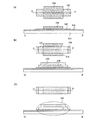
次に、本発明の微小構造体を作製する方法について、図面を用いて説明する。図面において、上側には上面図を示し、下側には上面図O−Pにおける断面図を示す。 Next, a method for manufacturing the microstructure of the present invention will be described with reference to the drawings. In the drawings, a top view is shown on the upper side, and a sectional view in the top view OP is shown on the lower side.
本発明の微小構造体は、絶縁性表面を有する基板(以下、絶縁基板という)上に形成することを特徴とする。絶縁性基板とは、ガラス基板、石英基板、プラスチック基板等である。さらに、金属等の導電性基板や、シリコン等の半導体性基板上に絶縁性を有する層を形成した基板を用いることも可能である。プラスチック基板に微小構造体を形成することにより、柔軟性が高く、薄型な半導体装置を形成することができる。またガラス基板を研磨等により薄くすることによって、薄型な半導体装置を形成することもできる。 The microstructure of the present invention is formed over a substrate having an insulating surface (hereinafter referred to as an insulating substrate). The insulating substrate is a glass substrate, a quartz substrate, a plastic substrate, or the like. Furthermore, it is also possible to use a conductive substrate such as a metal or a substrate in which an insulating layer is formed over a semiconductor substrate such as silicon. By forming a microstructure on a plastic substrate, a highly flexible and thin semiconductor device can be formed. In addition, a thin semiconductor device can be formed by thinning the glass substrate by polishing or the like.
まず、絶縁表面を有する基板101上に下地膜102を形成する(図1(A)参照)。下地膜102は酸化シリコン膜、窒化シリコン膜または酸化窒化シリコン膜などの絶縁層を単層または積層構造で形成することができる。本実施の形態では下地膜102として2層構造を用いる場合を説明するが、下地膜102は単層構造または2層以上の積層構造を用いても良い。
First, the
下地膜102の一層目としては、プラズマCVD法を用い、SiH4、NH3、N2O及びH2を反応ガスとして成膜される酸化窒化シリコン膜を10〜200nm(好ましくは50〜100nm)形成することができ、本実施の形態では、膜厚50nmの酸化窒化シリコン膜を形成する。次いで下地膜102の二層目に、プラズマCVD法を用い、SiH4及びN2Oを反応ガスとして成膜される酸化窒化シリコン膜を50〜200nm(好ましくは100〜150nm)の厚さに積層形成することができ、本実施の形態では膜厚100nmの酸化窒化シリコン膜を形成する。
As the first layer of the
次に、微小構造体を構成する第一の構造層103となる非晶質シリコン層または多結晶シリコン膜を成膜し、任意の形状にパターニングする(図1(A)参照)。多結晶シリコン膜は、珪素を有する材料から形成することができる。珪素を有する材料には、珪素からなる材料、ゲルマニウムを0.01〜4.5atomic%程度に有するシリコンゲルマ材料がある。また上記シリコン膜には、結晶状態を有するもの、非晶質状態を有するものを用いることができるが、本実施の形態では、非晶質シリコン膜を形成し、金属元素を用いた加熱処理により、結晶化された多結晶シリコン膜を用いる。加熱処理には、加熱炉、レーザ照射、若しくはレーザ光の代わりにランプから発する光の照射(以下、ランプアニールと表記する)、又はそれらを組み合わせて用いることができる。
Next, an amorphous silicon layer or a polycrystalline silicon film to be the first
上記のような構造層は、必要な厚さを得るために、多層構造とすることも可能である。たとえば、非晶質シリコン膜の成膜と、加熱処理による結晶化を繰り返すことによって多結晶シリコンの積層構造を形成することができる。この加熱処理によって、先に形成された多結晶シリコン膜内の応力を緩和し、膜剥がれや基板の変形を防ぐことができる。また、さらに膜内の応力を緩和するために、パターニングも含めて繰り返すこともできる。 The structural layer as described above may have a multilayer structure in order to obtain a necessary thickness. For example, a multilayer structure of polycrystalline silicon can be formed by repeating formation of an amorphous silicon film and crystallization by heat treatment. By this heat treatment, the stress in the previously formed polycrystalline silicon film can be relieved, and film peeling and substrate deformation can be prevented. Further, in order to relieve the stress in the film, it can be repeated including patterning.
また構造層は、結晶状態の異なる膜を積層して用いてもよい。例えば、非晶質シリコン膜と、多結晶シリコン膜との積層構造を用いることができる。 The structural layer may be formed by stacking films having different crystal states. For example, a stacked structure of an amorphous silicon film and a polycrystalline silicon film can be used.
このように積層構造を用いる場合、内部応力の大きい材料を構造層として利用する場合、一度に厚い構造層を成膜することができない。この場合には、成膜とパターニングとを繰り返し、構造層を形成することも可能である。 When a laminated structure is used in this way, when a material having a large internal stress is used as the structural layer, a thick structural layer cannot be formed at a time. In this case, the structural layer can be formed by repeating film formation and patterning.
また多結晶シリコンの作製において、レーザ照射を用いる場合、連続発振型のレーザビーム(CWレーザビーム)やパルス発振型のレーザビーム(パルスレーザビーム)を用いることができる。レーザビームとしては、Arレーザ、Krレーザ、エキシマレーザ、YAGレーザ、Y2O3レーザ、YVO4レーザ、YLFレーザ、YAlO3レーザ、ガラスレーザ、ルビーレーザ、アレキサンドライトレーザ、Ti:サファイヤレーザ、銅蒸気レーザまたは金蒸気レーザのうち一種または複数種を用いることができる。このようなレーザビームの基本波、及び当該基本波の第2高調波から第4高調波のレーザビームを照射することで、大粒径の結晶を得ることができる。例えば、Nd:YVO4レーザ(基本波1064nm)の第2高調波(532nm)や第3高調波(355nm)を用いることができる。このときレーザのエネルギー密度は0.01〜100MW/cm2程度(好ましくは0.1〜10MW/cm2)が必要である。そして、走査速度を10〜2000cm/sec程度として照射する。 When laser irradiation is used in the production of polycrystalline silicon, a continuous wave laser beam (CW laser beam) or a pulsed laser beam (pulse laser beam) can be used. As laser beams, Ar laser, Kr laser, excimer laser, YAG laser, Y 2 O 3 laser, YVO 4 laser, YLF laser, YAlO 3 laser, glass laser, ruby laser, alexandrite laser, Ti: sapphire laser, copper vapor One or a plurality of lasers or gold vapor lasers can be used. By irradiating the fundamental wave of such a laser beam and the second to fourth harmonics of the fundamental wave, a crystal having a large grain size can be obtained. For example, a second harmonic (532 nm) or a third harmonic (355 nm) of an Nd: YVO 4 laser (fundamental wave 1064 nm) can be used. Energy density of the laser is about 0.01 to 100 MW / cm 2 (preferably 0.1 to 10 MW / cm 2) is required. Then, irradiation is performed at a scanning speed of about 10 to 2000 cm / sec.
なお連続発振の基本波のレーザビームと連続発振の高調波のレーザビームとを照射するようにしてもよいし、連続発振の基本波のレーザビームとパルス発振の高調波のレーザビームとを照射するようにしてもよい。複数のレーザビームを照射することにより、エネルギーを補うことができる。 The continuous wave fundamental laser beam and the continuous wave harmonic laser beam may be irradiated, or the continuous wave fundamental laser beam and the pulsed harmonic laser beam may be irradiated. You may do it. By irradiating a plurality of laser beams, energy can be supplemented.
またパルス発振型のレーザビームであって、半導体膜がレーザ光によって溶融してから固化するまでに、次のパルスのレーザ光を照射できるような発振周波数でレーザを発振させるレーザビームを用いることもできる。このような周波数でレーザビームを発振させることで、走査方向に向かって連続的に成長した結晶粒を得ることができる。 具体的なレーザビームの発振周波数は10MHz以上であって、通常用いられている数十Hz〜数百Hzの周波数帯よりも著しく高い周波数帯を使用する。 It is also possible to use a pulse oscillation type laser beam that oscillates the laser at an oscillation frequency that allows irradiation of the next pulse of laser light after the semiconductor film is melted by the laser light and solidifies. it can. By oscillating the laser beam at such a frequency, crystal grains continuously grown in the scanning direction can be obtained. A specific oscillation frequency of the laser beam is 10 MHz or more, and a frequency band that is significantly higher than a frequency band of several tens to several hundreds Hz that is normally used is used.
その他の加熱処理として加熱炉を用いる場合には、非晶質半導体膜を400〜550℃で2〜20時間かけて加熱する。このとき、徐々に高温となるように温度を400〜550℃の範囲で多段階に設定するとよい。最初の400℃程度の低温加熱工程により、非晶質半導体膜の水素等が出てくるため、結晶化の際の膜荒れを低減することができる。
さらに、結晶化を促進させる金属元素、例えばニッケル(Ni)を非晶質半導体膜上に形成すると、加熱温度を低減することができ好ましい。金属元素としては、鉄(Fe)、ルチニウム(Ru)、ロジウム(Rh)、パラジウム(Pd)、オスミウム(Os)、イリジウム(Ir)、白金(Pt)、銅(Cu)、金(Au)、コバルト(Co)等の金属を用いることもできる。
In the case of using a heating furnace as other heat treatment, the amorphous semiconductor film is heated at 400 to 550 ° C. for 2 to 20 hours. At this time, the temperature may be set in multiple stages in the range of 400 to 550 ° C. so that the temperature gradually increases. In the first low-temperature heating process at about 400 ° C., hydrogen and the like of the amorphous semiconductor film are generated, so that film roughness during crystallization can be reduced.
Furthermore, it is preferable to form a metal element that promotes crystallization, such as nickel (Ni), over the amorphous semiconductor film because the heating temperature can be reduced. Examples of metal elements include iron (Fe), rutinium (Ru), rhodium (Rh), palladium (Pd), osmium (Os), iridium (Ir), platinum (Pt), copper (Cu), gold (Au), A metal such as cobalt (Co) can also be used.
さらに加熱炉に加えて、上記のようなレーザ照射を行って、多結晶シリコンを形成してもよい。 Furthermore, in addition to the heating furnace, polycrystalline silicon may be formed by performing laser irradiation as described above.
このように形成された多結晶シリコンは、金属元素を用いた加熱処理を行うことで、結晶構造が単結晶を用いた場合とほぼ同じであり、構造層の材料として使用されうる金属元素を用いない加熱処理によって作製される多結晶シリコンに比べて靭性が高い第一の構造層103を得ることができる。これは、金属元素を用いた加熱処理により結晶粒界が連続している多結晶シリコンを作ることができるからである。結晶粒界が連続している多結晶シリコンは、非晶質シリコンや、金属元素を用いない加熱処理によって得られる多結晶シリコンと異なり、結晶粒界で共有結合が途切れることが無い。そのため、結晶粒界が欠陥となって起こる応力集中が起こらず、結果として金属元素を用いずに形成された多結晶シリコンに比べて破壊応力が高くなる。さらに、結晶粒界が連続していることによって電子の移動度が大きいため、構造体を静電力で制御する場合の材料として適している。
The polycrystalline silicon formed in this way is subjected to heat treatment using a metal element, so that the crystal structure is almost the same as when a single crystal is used, and a metal element that can be used as a material for the structural layer is used. Thus, the first
さらに、第一の構造層103は、結晶化を助長させる金属元素を含むと、導電性を有することができ、構造体を静電力で制御する本発明の半導体装置に好適である。
Further, when the first
また、金属元素は半導体装置の汚染源となるため、結晶化した後に除去することも可能である。この場合、金属元素を用いた加熱処理の後、シリコン膜上にゲッタリングシンクとなる層を形成し、加熱することにより、金属元素をゲッタリングシンクへ移動させることができる。ゲッタリングシンクには、多結晶半導体膜や不純物が添加された半導体膜を用いることができる。例えば、半導体膜上にアルゴン等の不活性元素が添加された多結晶半導体膜を形成し、これをゲッタリングシンクとして適用することができる。不活性元素を添加することによって、多結晶半導体膜にひずみを生じさせることができ、ひずみにより効率的に金属元素を捕獲することができる。またリン等の元素を添加した半導体膜を形成することによって、金属元素を捕獲することもできる。 Further, since the metal element becomes a contamination source of the semiconductor device, it can be removed after crystallization. In this case, after the heat treatment using the metal element, a layer serving as a gettering sink is formed over the silicon film, and the metal element can be moved to the gettering sink by heating. As the gettering sink, a polycrystalline semiconductor film or a semiconductor film to which impurities are added can be used. For example, a polycrystalline semiconductor film to which an inert element such as argon is added can be formed over the semiconductor film, and this can be used as a gettering sink. By adding an inert element, the polycrystalline semiconductor film can be distorted, and the metal element can be efficiently captured by the distortion. A metal element can also be captured by forming a semiconductor film to which an element such as phosphorus is added.
このような工程によって作製された第一の構造層103を用いることができる。また、第一の構造層103に導電性が必要な場合は、第一の構造層103に燐や砒素、硼素等の不純物元素を添加することも可能である。導電性を持たせた構造体は、導電性を有する構造を有している静電力で制御する本発明の半導体装置に好適である。
The first
第一の構造層103に不純物領域を形成して導電性を高めてもよい。不純物領域は、フォトリソグラフィ法によりレジストマスクを形成し、不純物元素を添加して形成することができる。不純物元素を添加する方法は、イオンドープ法またはイオン注入法で行うことができる。N型を付与する不純物元素として、典型的にはリン(P)または砒素(As)を用い、p型を付与する不純物元素としては、ボロン(B)を用いる。n型不純物領域、およびp型不純物領域には、1×10²⁰〜1×10²¹/cm3の濃度範囲で不純物元素が添加された不純物領域を形成することができる。
An impurity region may be formed in the
不純物領域を形成した後、不純物元素を活性化するために加熱処理を行ってもよい。加熱処理は、上述した条件で行えばよい。 After the impurity region is formed, heat treatment may be performed to activate the impurity element. The heat treatment may be performed under the conditions described above.
次に犠牲層104を成膜し、任意の形状にパターニングする(図1(A)参照)。犠牲層104は、タングステン等の金属、やシリコンを有する化合物(例えばシリコン酸化物やシリコン窒化物)、金属とシリコンなどの元素の化合物である金属化合物を材料とし、スパッタリング法やCVD法等を用いて成膜することができる。パターニングには、フォトリソグラフィ法を用いてレジストマスクを形成し、異方性のドライエッチングを行う。犠牲層とは、後の工程で除去される層を指し、犠牲層を除去することによって空間が設けられることとなる。このような犠牲層は、金属、金属化合物、シリコン、シリコン酸化物、またはシリコン窒化物を有する材料から形成することができる。また犠牲層は導電層であっても、絶縁層であってもよい。
Next, a
犠牲層104の膜厚は、犠牲層104の材料や、構造体の構造および動作方法、犠牲層を除去するためのエッチング方法等、様々な要因を考慮して決定される。例えば、犠牲層104が薄すぎればエッチング剤が拡散せずにエッチングされない。また、エッチング後に、犠牲層104上に形成される構造層が座屈する(はりつき、スティッキングともいう)といった現象も生じる。さらに、構造体を静電力で動作させる場合、犠牲層が厚すぎると駆動できなくなる恐れがある。そのため、静電力による駆動を行う場合、犠牲層104は例えば0.5μm以上3μm以下の厚さを有し、1μm〜2.5μmを有すると好ましい。
The thickness of the
また、内部応力の大きい材料を犠牲層として利用する場合、一度に厚い犠牲層を成膜することが難しい。この場合には、成膜やパターニングを繰り返し、犠牲層を厚く形成することも可能である。すなわち犠牲層は、単層構造であっても、積層構造であってもよい。 Further, when a material having a large internal stress is used as a sacrificial layer, it is difficult to form a thick sacrificial layer at a time. In this case, the sacrificial layer can be formed thick by repeating film formation and patterning. That is, the sacrificial layer may have a single layer structure or a laminated structure.
次に微小構造体の上部を構成する第二の構造層105を形成する。第二の構造層105は、非晶質シリコン膜または多結晶シリコン膜を形成し、任意の形状にパターニングする(図1(B)参照)。このとき、犠牲層104の一部が露出するようにする(図1(B)上面図参照)。第二の構造層105は、第一の構造層103と同様な材料、同様な結晶構造有するものを用いることができる。そして、第一の構造層103と同様に、金属元素を用いた加熱処理によって多結晶シリコン層を作製することができる。
Next, a second
このような工程によって作製された多結晶シリコンは、第二の構造層105に用いることができる。加熱処理に用いられた金属元素をそのまま有することにより、多結晶シリコンは導電性を有することができる。また、第二の構造層105に導電性が必要な場合は、第一の構造層103と同様に不純物元素を添加することも可能である。
Polycrystalline silicon manufactured through such a process can be used for the second
不純物領域を形成した後、不純物元素の活性化を行ってもよい。活性化手段は、第一の構造層103の場合と同様である。
After the impurity region is formed, the impurity element may be activated. The activation means is the same as in the case of the first
上記第二の構造層105の成膜は、必要な厚さを得るために、第一の構造層103と同様に多層構造とすることも可能である。
The second
第二の構造層105の材料および膜厚は、第一の構造層103との密着性、犠牲層104の厚さ、第二の構造層105の材料、構造体の構造、または犠牲層エッチングの方法等、様々な要因を考慮して決定することができる。例えば、本実施形態のシリコン膜を用いて第二の構造層105を作製する場合、膜厚は1μm以上10μm以下を有することが好ましい。
The material and film thickness of the second
このような第二の構造層105の材料として内部応力の分布差が大きい材料を用いると第二の構造層105に反りが生じる恐れがある。しかしながら、第二の構造層105の反りを利用して構造体を構成することも可能である。
When a material having a large internal stress distribution difference is used as the material of the second
また、第二の構造層105を厚く成膜すると内部応力に分布が生じ、反りや座屈(はりつき、スティッキングともいう)の原因となる。逆に、第二の構造層105の厚さが薄いと、犠牲層エッチング時に用いる溶液の表面張力によって構造体が座屈するおそれがある。これらを考慮して、第二の構造層105の膜厚を決定することができる。
Further, when the second
次に、犠牲層104をエッチングにより除去する(図1(C)参照)。エッチングは、犠牲層104の材料によって適したエッチング剤及びエッチング方法により行うことができる。エッチング方法には、ウエットエッチング法、またはドライエッチング法がある。
Next, the
例えば、犠牲層がタングステン(W)である場合、28%のアンモニアと31%の過酸化水素水を1:2で混合した溶液に20分程度漬けることで行う。犠牲層が二酸化珪素の場合は、フッ酸49%水溶液1に対してフッ化アンモニウムを7の割合で混合したバッファードフッ酸を用いる。 For example, when the sacrificial layer is tungsten (W), the sacrificial layer is immersed in a solution in which 28% ammonia and 31% hydrogen peroxide solution are mixed at a ratio of 1: 2 for about 20 minutes. When the sacrificial layer is silicon dioxide, buffered hydrofluoric acid in which ammonium fluoride is mixed in a ratio of 7 to 49% aqueous solution 1 of hydrofluoric acid is used.
ウエットエッチング後の乾燥に際しては、毛管現象による構造体の座屈を防ぐため、粘性の低い有機溶媒(例えばシクロヘキサン)を用いてリンスを行う、若しくは低温低圧の条件で乾燥させる、またはこの両者の組み合わせによって行うことができる。 When drying after wet etching, in order to prevent buckling of the structure due to capillary action, rinse with a low-viscosity organic solvent (for example, cyclohexane), or dry under low temperature and low pressure conditions, or a combination of both Can be done by.
また、犠牲層は、大気圧など高圧の条件において、F2やXeF2を用いてドライエッチングを行うことができる。毛管現象による構造体の座屈を防ぐため、構造体表面に撥水性を持たせるプラズマ処理を行うこともできる。 The sacrificial layer can be dry-etched using F 2 or XeF 2 under high pressure conditions such as atmospheric pressure. In order to prevent buckling of the structure due to capillary action, plasma treatment for imparting water repellency to the surface of the structure can also be performed.
本実施の形態において、犠牲層104の一部は露出しているため、コンタクトホールを形成することなく、犠牲層104を除去することができる。
In this embodiment mode, part of the
また第二の構造層105や犠牲層104を覆うように絶縁層等を形成する場合、当該絶縁層にコンタクトホールを形成し、コンタクトホールを介してエッチング剤を導入することで、犠牲層104を除去することができる。
In the case where an insulating layer or the like is formed so as to cover the second
このような工程を用いて犠牲層104をエッチング除去することによって、構造体106を作製することができる。
The
構造体106は、犠牲層104をエッチング除去することによって、基板または基板に接合した第一の構造層103に対して、第二の構造層105が固定されていない、または接していない部分を有する構造となる。このような構造とは、たとえば、図1(C)に示したような梁構造がある。梁構造とは、柱部分と梁部分とを有する構造である。
The
また、構造体106を静電力で可動させる場合、下地膜102の下に共通電極や制御電極等として使用することができる導電層107を形成してもよい(図2(A)参照)。また、下地膜102を積層構造にしている場合、下地膜102の間に導電層107を形成することも可能である(図2(B)参照)。導電層107は、タングステン等の金属や導電性を有する物質を材料として、CVD法等により成膜することができる。また、必要に応じて任意の形状にパターニングしても良い。
In the case where the
構造体106を構成する層が、上面からみて角を有するパターンの場合、角の部分が丸みを帯びた形状にパターニングすることが好ましい。これは、後に除去される犠牲層104についても同様である。図7(A)には、導電層107および犠牲層104を形成してパターニングした上面図、及び図7(B)にはその断面図を示す。このように角をとって丸みを帯びた状態にパターニングすることによって、ゴミの発生を抑え歩留まりを向上させることができる。
When the layer forming the
このように構造体106を構成する層は、できる限り滑らかな形状にすることが望ましい。このように鋭い分のない形状にすることによって、ごみの発生を抑え、破壊の原因となる亀裂が入りにくくなる。
As described above, it is desirable that the layers constituting the
また、上記の工程では犠牲層104の上に第二の構造層105を成膜しているが、犠牲層104の上に絶縁層を成膜し、その後第二の構造層105を成膜することも可能である。
すなわち本発明は、構造層に金属元素を用いて形成された多結晶シリコンを用いることを特徴としており、その他の構成には限定されない。
In the above process, the second
That is, the present invention is characterized by using polycrystalline silicon formed using a metal element in the structural layer, and is not limited to other structures.
このように、犠牲層104と、第二の構造層105との間に絶縁層を形成することで、犠牲層104を除去する際に、絶縁層によって第二の構造層105を保護し、第二の構造層105のダメージを低減することができる。
In this manner, by forming the insulating layer between the
以上説明した、構造体106を作製する方法においては、第一の構造層103、第二の構造層105の材料、犠牲層104の材料、および犠牲層を除去するエッチング剤の適当な組み合わせを決定する。例えば、エッチング剤を特定のものに決めた場合、第一の構造層103、第二の構造層105の材料に比べて、エッチングレートが大きい材料を用いて犠牲層104を構成すればよい。
In the method for manufacturing the
また、第一の構造層103、第二の構造層105を構成する多結晶シリコン層は、上記の工程を用いて結晶化させた多結晶シリコンを有する層と、非晶質シリコンを有する層とを積層することができることは上述のとおりである。このように積層構造を有する構造層を用いることで、しなやかさと硬さを併せ持つ構造層を得ることができる。また、積層させる層の厚さの比率によって、しなやかさと堅さのバランスを決めることができる。
The polycrystalline silicon layers constituting the first
また、ニッケルシリサイドのような珪素合金は一般に強度が高いことが知られている。半導体膜の加熱処理時に用いる金属元素を半導体膜中の全体または選択的に残しておき、適当な熱処理を加えることで、さらに硬く、導電性の高い構造体を作製することができる。 Further, it is known that a silicon alloy such as nickel silicide is generally high in strength. By leaving the metal element used in the heat treatment of the semiconductor film entirely or selectively in the semiconductor film and applying an appropriate heat treatment, a harder and more conductive structure can be manufactured.
また、上記のような結晶化に用いた金属元素を残した層と、多結晶シリコンを有する層とを積層させることで、導電性に優れ、しなやかな材料を得ることができる。また、非晶質シリコンを有する層とシリサイドを有する層を積層することで、導電性に優れ、硬い材料にすることができる。 In addition, by laminating the layer including the metal element used for crystallization as described above and the layer including polycrystalline silicon, a flexible material with excellent conductivity can be obtained. In addition, by stacking a layer having amorphous silicon and a layer having silicide, a hard material having excellent conductivity can be obtained.
また、金属元素を全面に添加しレーザ照射や加熱処理を行った場合、シリコンの結晶成長方向が基板に対して垂直方向に進み、金属を選択的に添加しレーザ照射や加熱処理をおこなったり、または金属元素を用いないで結晶化した場合、結晶成長方向が基板に対して平行方向に進む。この結晶方向の異なる層を2層以上積層することで、さらに靭性に優れた材料を得ることができる。結晶方向が異なる膜が積層しているため、一つの層で破壊が起きても、結晶方向の違う層には亀裂が伝播しにくい。その結果として破壊が起こりにくく、強度の高い第二の構造層105を作製することができる。
When a metal element is added to the entire surface and laser irradiation or heat treatment is performed, the crystal growth direction of silicon advances in a direction perpendicular to the substrate, and metal is selectively added to perform laser irradiation or heat treatment. Alternatively, when crystallization is performed without using a metal element, the crystal growth direction proceeds in a direction parallel to the substrate. By laminating two or more layers having different crystal directions, a material having further excellent toughness can be obtained. Since films with different crystal directions are stacked, cracks are unlikely to propagate to layers with different crystal directions even if a single layer breaks down. As a result, the second
そして非晶質シリコンを有する層、多結晶シリコンを有する層、またはニッケルシリサイドを有する層は、必要な厚さを得るために、成膜を繰り返して積層させることも可能である。 The layer having amorphous silicon, the layer having polycrystalline silicon, or the layer having nickel silicide can be stacked by repeated film formation in order to obtain a required thickness.
図10(A)に示すように、様々な性質を持つシリコンおよびシリコンの化合物を積層させることができる。図10(A)には、基板101上に、非晶質シリコンを有する層150、多結晶シリコンを有する層151、およびニッケルシリサイドを有する層152を積層させた場合を示す。本発明は、構造体を構成する層を任意に選択し、積層させることができる。また、上記工程の積層は、容易に行うことが可能である。したがって、所望の性質を有する第二の構造層105を容易に作製することが可能である。
As shown in FIG. 10A, silicon having various properties and silicon compounds can be stacked. FIG. 10A illustrates the case where a
さらに、上記工程のように金属を用いた結晶化は、選択的に金属元素を塗布することで、部分的に結晶化を行うこともできる。たとえば、上記第二の構造層105の、下に犠牲層104がある部分のみ金属を塗布し、結晶化することができる。
Furthermore, the crystallization using a metal as in the above-described step can be partially performed by selectively applying a metal element. For example, the metal can be applied and crystallized only in the portion of the second
上記のような結晶化は、選択的にレーザを照射することで、部分的に結晶化することもできる。たとえば、上記第二の構造層105の、下に犠牲層104がある部分154のみ結晶化することができる。さらには、レーザ条件を変化させることにより図10(B)に示す梁構造の柱部分155のみに非晶質シリコンを残し、梁部分を結晶化させることも可能である。このように、結晶状態の異なるシリコンを用い、微小構造体を形成することができる。
The crystallization as described above can be partially crystallized by selective laser irradiation. For example, only the
上記工程のように、金属元素を用いて加熱処理を行う場合、金属元素を用いずに行う加熱処理に比べて低温で結晶化することができるため、構造体を形成する基板に使用できる材料の幅が広がる。例えば、半導体膜を加熱のみで結晶化させる場合、1000℃程度の温度で1時間程度の加熱を行う必要があり、熱に被弱なガラス基板や、融点が1000℃以下の金属を用いることができない。しかしながら、上記工程を用いることによって、ゆがみ点が593℃であるガラス基板等を用いることが可能になる。 When heat treatment is performed using a metal element as in the above-described process, crystallization can be performed at a lower temperature than heat treatment performed without using a metal element, so that a material that can be used for a substrate for forming a structure is used. The width expands. For example, when a semiconductor film is crystallized only by heating, it is necessary to perform heating for about 1 hour at a temperature of about 1000 ° C., and a glass substrate vulnerable to heat or a metal having a melting point of 1000 ° C. or less is used. Can not. However, by using the above process, a glass substrate or the like having a distortion point of 593 ° C. can be used.
このように本発明は、絶縁表面上に微小構造体を作製することができる。
そして、当該半導体素子によって電気回路を形成することができ、微小構造体の制御を行うことができる。このような微小構造体を有する半導体装置は、作製コストを削減することができる。また従来のように電気回路を別途形成し、微小構造体と電気的に接続する構成と比べ、本発明の半導体装置の作製方法により量産性を向上させることができる。
As described above, the present invention can produce a microstructure on an insulating surface.
Then, an electric circuit can be formed using the semiconductor element, and the microstructure can be controlled. A semiconductor device having such a microstructure can reduce manufacturing costs. In addition, mass productivity can be improved by the method for manufacturing a semiconductor device of the present invention, as compared with a structure in which an electric circuit is separately formed and electrically connected to a microstructure as in the conventional case.
(実施の形態2)
本実施の形態では、上記実施の形態とは異なり、多結晶シリコンを絶縁層で狭持した構造体について、図3を用いて説明する。図面において、上側には上面図を示し、下側には上面図O−Pにおける断面図を示す。
(Embodiment 2)
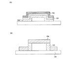
In this embodiment mode, unlike the above embodiment mode, a structure in which polycrystalline silicon is sandwiched between insulating layers will be described with reference to FIGS. In the drawings, a top view is shown on the upper side, and a sectional view in the top view OP is shown on the lower side.
図3(A)に示すように、絶縁基板201上に下地膜202、犠牲層203を形成する。これらの作製方法は、実施の形態1を参照することができる。そして構造体を構成する第一の絶縁層204を形成する。第一の絶縁層には、無機材料又は有機材料を用いることができる。無機材料は、酸化珪素、窒化珪素を用いることができる。有機材料はポリイミド、アクリル、ポリアミド、ポリイミドアミド、ベンゾシクロブテン、シロキサン、ポリシラザンを用いることができる。シロキサンは、シリコン(Si)と酸素(O)との結合で骨格構造が構成される。置換基として、少なくとも水素を含む有機基(例えばアルキル基、芳香族炭化水素)が用いられる。置換基として、フルオロ基を用いてもよい。または置換基として、少なくとも水素を含む有機基と、フルオロ基とを用いてもよい。ポリシラザンは、珪素(Si)と窒素(N)の結合を有するポリマー材料を出発原料として形成される。
As shown in FIG. 3A, a
特に、第一の絶縁層204に無機材料を用いる場合、被形成面の表面を酸化、又は窒化することによって作製することができる。このような酸化、又は窒化する手段として、高密度プラズマ処理がある。高密度プラズマ処理とは、プラズマ密度が1×1011cm−3以上、好ましくは1×1011cm−3から9×1015cm−3以下であり、マイクロ波(例えば周波数2.45GHz)といった高周波を用いたプラズマ処理である。このような条件でプラズマを発生させると、低電子温度が0.2eVから2eVとなる。このように低電子温度が特徴である高密度プラズマは、活性種の運動エネルギーが低いため、プラズマダメージが少なく、欠陥の少ない膜を形成することができる。
In particular, when an inorganic material is used for the first insulating
このようなプラズマ処理を可能とする成膜室に、第一の犠牲層203まで形成された基板を配置し、プラズマ発生用の電極、所謂アンテナと被形成体との距離を20mmから80mm、好ましくは20mmから60mmとして成膜処理を行う。このような高密度プラズマ処理は、低温プロセス(基板温度400℃以下)の実現が可能となる。そのため、耐熱性の低いガラスやプラスチックを絶縁基板201として利用することができる。
A substrate formed up to the first
このような絶縁層の成膜雰囲気は窒素雰囲気、又は酸素雰囲気とすることができる。窒素雰囲気とは、代表的には、窒素と希ガスとの混合雰囲気、又は窒素と水素と希ガスとの混合雰囲気である。希ガスは、ヘリウム、ネオン、アルゴン、クリプトン、キセノンの少なくとも1つを用いることができる。また酸素雰囲気とは、代表的には、酸素と希ガスとの混合雰囲気、酸素と水素と希ガスとの混合雰囲気、又は一酸化二窒素と希ガスとの混合雰囲気である。希ガスは、ヘリウム、ネオン、アルゴン、クリプトン、キセノンの少なくとも1つを用いることができる。 The film formation atmosphere of such an insulating layer can be a nitrogen atmosphere or an oxygen atmosphere. The nitrogen atmosphere is typically a mixed atmosphere of nitrogen and a rare gas, or a mixed atmosphere of nitrogen, hydrogen, and a rare gas. As the rare gas, at least one of helium, neon, argon, krypton, and xenon can be used. The oxygen atmosphere is typically a mixed atmosphere of oxygen and a rare gas, a mixed atmosphere of oxygen, hydrogen, and a rare gas, or a mixed atmosphere of dinitrogen monoxide and a rare gas. As the rare gas, at least one of helium, neon, argon, krypton, and xenon can be used.
このように形成された絶縁層は、他の被膜に与えるダメージが少なく、緻密なものとなる。また高密度プラズマ処理により形成された絶縁層は、当該絶縁層と接触する界面状態を改善することができる。例えば高密度プラズマ処理を用いて第一の絶縁層204を形成すると、被形成面との界面状態を改善することができる。このような絶縁層を構造体層上に成膜することによって、構造体に与えるダメージを少なくすることができる。
The insulating layer formed in this way has little damage to other coatings and becomes dense. An insulating layer formed by high-density plasma treatment can improve an interface state in contact with the insulating layer. For example, when the first insulating
ここでは、ゲート絶縁層の成膜に高密度プラズマ処理を用いる場合を説明したが、半導体膜に高密度プラズマ処理を施してもよい。高密度プラズマ処理によって、半導体膜表面の改質を行うことができる。その結果、界面状態を改善でき、半導体素子の電気特性を向上させることができる。 Although the case where high-density plasma treatment is used for forming the gate insulating layer is described here, high-density plasma treatment may be performed on the semiconductor film. The semiconductor film surface can be modified by high-density plasma treatment. As a result, the interface state can be improved, and the electrical characteristics of the semiconductor element can be improved.
さらに、第一の絶縁層204の成膜のみではなく、下地膜202を成膜する場合にも、高密度プラズマ処理を用いて作製することができる。
Furthermore, not only the first insulating
次いで図3(B)に示すように、第一の絶縁層204上に、多結晶シリコンを有する層(構造層)205を形成し、当該層205を覆うように第二の絶縁層206を形成する。多結晶シリコンを有する層(構造層)205は、上記実施の形態を参照することができる。また第二の絶縁層206は、第一の絶縁層204を参照することができる。
Next, as illustrated in FIG. 3B, a layer (structural layer) 205 including polycrystalline silicon is formed over the first insulating
その後、犠牲層203が露出するよう、第一の絶縁層204および第二の絶縁層206を任意の形状にパターニングを行う(図3(B)上面図参照)。
After that, the first insulating
次に、犠牲層203をエッチングにより除去する(図3(C)参照)。犠牲層203のエッチングは、上記実施の形態を参照することができる。
Next, the
また、構造体207を静電力で可動させる場合、下地膜202の下に共通電極や制御電極等として使用することができる導電層208を形成してもよい(図4(A)参照)。また、下地膜202を積層構造にしている場合、下地膜202の間に導電層208を形成することも可能である(図4(B)参照)。導電層208は、タングステン等の金属や導電性を有する物質を材料として、CVD法等により成膜することができる。また、必要に応じて任意の形状にパターニングしても良い。
In the case where the
構造体207を構成する層が、上面からみて角を有するパターンの場合、角の部分が丸みを帯びた形状にパターニングすることが好ましい。これは、後に除去される犠牲層203についても同様である。図9(A)には、導電層208および犠牲層203を形成してパターニングした上面図、及び図9(B)にはその断面図を示す。このように角をとって丸みを帯びた状態にパターニングすることによって、ゴミの発生を抑え歩留まりを向上させることができる。
In the case where the layer constituting the
なお、本実施の形態は上記実施の形態と自由に組み合わせて行うことができる。 Note that this embodiment mode can be freely combined with the above embodiment modes.
(実施の形態3)
本実施の形態では、上記実施の形態で作製した微小構造体の説明を、図面を用いて説明する。
(Embodiment 3)
In this embodiment, the microstructure manufactured in the above embodiment will be described with reference to drawings.
図5に、上記実施の形態で説明した微小構造体の作製方法を応用して作製した微小構造体301の断面図を示す。微小構造体301は、基板300上に下地膜305、第1の導電層303、第1の絶縁層306が形成され、第1の絶縁層上に、半導体層302および第2の絶縁層307を積層して形成される構造層を有する。構造層の上部には、第3の絶縁層309が部分的領域に形成され、第3の絶縁層に設けられたコンタクトホールを介して、第2の導電層304が第1の導電層および半導体層と電気的に接続される。
FIG. 5 shows a cross-sectional view of a
ここで、構造層を形成する半導体層302に不純物元素や金属元素を添加すれば、半導体層302が導電性を有するため、構造層と第1の導電層とで容量(コンデンサ)を構成することができる。そして、このように作製された構造層は、静電力や圧力、加速度等の外力等を受けて可動することができるため、上記容量は可変容量(可変コンデンサ)となる。したがって、微小構造体301は外力を受けて容量が変化するセンサとして機能することができる。
Here, if an impurity element or a metal element is added to the
したがって、図5に示す微小構造体は、図6で説明した半導体装置11において、外力を検知するセンサ16の役割を担うことができる。 Therefore, the microstructure shown in FIG. 5 can serve as the sensor 16 that detects an external force in the semiconductor device 11 described with reference to FIG.
また、図5に示す微小構造体301において、構造層を、熱膨張率の異なる2種類の物質を積層させたバイメタル構造として作製することができる。この場合、構造層 は温度変化によって可動するので、微小構造体301は、温度検知素子として利用することも可能である。
In the
また図8には、上記実施の形態で説明した微小構造体の作製方法を応用して作製した微小構造体の斜視図を示す。微小構造体310は、基板316上に下地膜317、犠牲層314、および半導体層で形成される構造層315を有する。微小構造体310は、構造層315が可動する片持ち梁313、ならびにその両側にある第1の電極311および第2の電極312を構成し、少なくとも可動する片持ち梁313の下に形成されていた犠牲層314がエッチングにより除去されている。
FIG. 8 is a perspective view of a microstructure manufactured by applying the manufacturing method of the microstructure described in the above embodiment mode. The
このように作製された微小構造体310は、可動する片持ち梁313が可動して、第1の電極311又は第2の電極312と接触する、スイッチ素子として機能することができる。また、可動する片持ち梁313に一定の振動を加えておき、微小構造体310にコリオリの力が働いたときに、それを検知する角運動量センサとして使用することも可能である。
The
このような微小構造体を用いてスイッチ素子を作製すれば、オフ時にスイッチを介した信号伝達経路が完全に絶縁され、オン時には低抵抗の信号伝達経路を形成することができる。また、スイッチのオン・オフを制御する制御系と、信号伝達経路とを絶縁することができ、挿入損失の少ないスイッチを作製することができる。 When a switch element is manufactured using such a microstructure, a signal transmission path through the switch is completely insulated when turned off, and a low-resistance signal transmission path can be formed when turned on. In addition, a control system that controls on / off of the switch and the signal transmission path can be insulated, and a switch with low insertion loss can be manufactured.
また、上記のように作製した微小構造体は、同じ形状でありながら制御方法を変えることによって素子としても、センサとしても利用することができる場合がある。さらには、制御方法を変えることにより、アクチュエータとしても機能させることができ、上記例の微小構造体は、図6に示した半導体装置11において、構造体部13を形成することができる。 In addition, the microstructure manufactured as described above may be used as an element or a sensor by changing a control method while having the same shape. Further, the structure can be made to function as an actuator by changing the control method, and the microstructure in the above example can form the structure portion 13 in the semiconductor device 11 shown in FIG.
本実施例では、上記実施の形態1において図1、2を用いて説明した第二の構造層105や、実施の形態2において図3、4を用いて説明した構造層205のように、半導体層によって構成される構造層の作製方法についての例を示す。
In this example, a semiconductor such as the second
例えば、図10(A)で示したように、構造体が有する構造層は、上記の工程を用いて結晶化させた多結晶シリコンを有する層と、非晶質シリコンを有する層とを積層させて形成することができる。 For example, as illustrated in FIG. 10A, the structure layer included in the structure is formed by stacking a layer including polycrystalline silicon crystallized using the above steps and a layer including amorphous silicon. Can be formed.
上記例で示す多結晶シリコンを有する層と非晶質シリコンを有する層のように、結晶状態の異なるシリコン層は、異なった機械的特性を有する。したがって、上記例のように積層させたり、選択的な領域に形成して構造層を形成することで、様々な用途に応じた構造体を作製することができる。 Like the layer having polycrystalline silicon and the layer having amorphous silicon shown in the above example, silicon layers having different crystal states have different mechanical characteristics. Therefore, by stacking as in the above example or forming the structure layer in a selective region, structures corresponding to various applications can be manufactured.
<複合弾性率およびインデンテーション硬さの測定>
結晶状態が異なるシリコン層の機械的特性の違いを調べるため、CVD法を用いて成膜した非晶質シリコンを有する層と、多結晶シリコンを有する層の複合弾性率、およびインデンテーション硬さの測定を行った。ここで、多結晶シリコンを有する層は、非晶質シリコンを有する層を金属触媒を用いてレーザー結晶化させたものである。
<Measurement of composite elastic modulus and indentation hardness>
In order to investigate the difference in the mechanical properties of silicon layers with different crystal states, the composite elastic modulus and indentation hardness of the layer having amorphous silicon and the layer having polycrystalline silicon formed by CVD are used. Measurements were made. Here, the layer having polycrystalline silicon is obtained by laser crystallization of a layer having amorphous silicon using a metal catalyst.
試料に用いた非晶質シリコンを有する層は、石英基板上に、下地層として厚さ50nmの窒化シリコン層、および厚さ100nmの酸化シリコン層をCVD法により形成し、その下地層上に、非晶質シリコン層をCVD法によって成膜した。また、試料に用いた多結晶シリコンを有する層は、連続発振型のレーザを用いて、上記と同様に形成した非晶質シリコンを有する層を結晶化させた。ここで、結晶化に用いたレーザのエネルギー密度は9〜9.5W/cm2、走査速度は35cm/secとした。ここで、試料の非晶質シリコンを有する層は66nmの厚さで成膜し、レーザ照射によって結晶化した多結晶シリコンを有する層の厚さは約60nmであった。 The layer having amorphous silicon used for the sample was formed by forming a silicon nitride layer with a thickness of 50 nm and a silicon oxide layer with a thickness of 100 nm as a base layer on a quartz substrate by a CVD method. An amorphous silicon layer was formed by a CVD method. In addition, the layer having polycrystalline silicon used for the sample was crystallized from a layer having amorphous silicon formed in the same manner as described above by using a continuous wave laser. Here, the energy density of the laser used for crystallization was 9 to 9.5 W / cm 2 , and the scanning speed was 35 cm / sec. Here, the layer having amorphous silicon as a sample was formed to a thickness of 66 nm, and the thickness of the layer having polycrystalline silicon crystallized by laser irradiation was about 60 nm.
測定は、三角錐形の圧子を試料に押し込むナノインデンテーション測定によって行った。測定条件は圧子の単一押し込みであり、使用した圧子はダイヤモンド製のBerkovich圧子である。したがって、圧子の弾性率は約1000GPa、ポアソン比は約0.1である。 The measurement was performed by nanoindentation measurement in which a triangular pyramid indenter was pushed into the sample. The measurement condition was a single indentation of the indenter, and the indenter used was a Berkovich indenter made of diamond. Therefore, the indenter has an elastic modulus of about 1000 GPa and a Poisson's ratio of about 0.1.
測定した複合弾性率は下記式(1)で表される、試料および圧子の弾性率を複合した弾性率である。式(1)においてErは複合弾性率、Eはヤング率、νはポアソン比である。また、式の第1項(sampleで示す項)は試料の弾性率が寄与する項であり、第2項(indenterで示す項)は圧子の弾性率が寄与する項である。 The measured composite elastic modulus is an elastic modulus obtained by combining the elastic modulus of the sample and the indenter represented by the following formula (1). In the formula (1), Er is a composite elastic modulus, E is a Young's modulus, and ν is a Poisson's ratio. In addition, the first term (term indicated by sample) in the equation is a term contributed by the elastic modulus of the sample, and the second term (term indicated by indenter) is a term contributed by the elastic modulus of the indenter.
式に示されるように、複合弾性率は、試料の弾性率が寄与する第1項と、圧子の弾性率が寄与する第2項との和で求められる。しかしながら、圧子の弾性率は試料に比べて非常に大きいため、第2項は無視することができ、複合弾性率は近似的に試料の弾性率を示す。 As shown in the equation, the composite elastic modulus is obtained by the sum of the first term contributed by the elastic modulus of the sample and the second term contributed by the elastic modulus of the indenter. However, since the elastic modulus of the indenter is much larger than that of the sample, the second term can be ignored, and the composite elastic modulus approximately represents the elastic modulus of the sample.
また、インデンテーション硬さとは、インデンテーション法によって測定される硬さであり、圧子の最大圧入加重を、最大圧入時の射影面積で割って求められる。ここで、圧入時の射影面積は、圧子の幾何学的な形状と、圧子が試料を押し込んだ時の接触深さによって求められる。このインデンテーション硬さに76を乗じることによって、硬さの指標として一般的に使用されているビッカース硬さと等価に扱うことができる。 The indentation hardness is hardness measured by an indentation method, and is obtained by dividing the maximum press-fit weight of the indenter by the projected area at the time of maximum press-fit. Here, the projected area at the time of press-fitting is determined by the geometric shape of the indenter and the contact depth when the indenter pushes the sample. By multiplying this indentation hardness by 76, it can be handled equivalent to the Vickers hardness generally used as an index of hardness.

表1に、多結晶シリコンを有する層と、非晶質シリコンを有する層の複合弾性率およびインデンテーション硬さの測定結果を示す。
結果は3回の測定結果の平均値を示している。
Table 1 shows the measurement results of the composite elastic modulus and indentation hardness of the layer having polycrystalline silicon and the layer having amorphous silicon.
The result has shown the average value of 3 times of measurement results.
表1に示す結果より、多結晶シリコンを有する層は、非晶質シリコンを有する層よりも高い弾性率を有する。すなわち、構造を曲げるような力が働いた場合に、多結晶シリコンを有する層は非晶質シリコンを有する層とよりも、曲げによる破壊に強いということを示している。 From the results shown in Table 1, the layer having polycrystalline silicon has a higher elastic modulus than the layer having amorphous silicon. That is, when a force that bends the structure is applied, the layer having polycrystalline silicon is more resistant to breakage due to bending than the layer having amorphous silicon.
さらに、表1に示す結果より、多結晶シリコンを有する層は非晶質シリコンを有する層よりも硬いことが示されている。
このように弾性率や硬さの異なる半導体層を積層することで、曲げる力に対して強いしなやかさと、硬さを併せ持つ構造体を作製することができる。例えば上記の層を積層させることによって、多結晶シリコンを有する層の結晶欠陥から破壊がおきても、非晶質シリコンを有する層には破壊が伝播しにくいため、多結晶シリコンを有する層と非晶質シリコンを有する層の間で破壊を止めることができる。このように、積層させる層の厚さの比率によって、しなやかさと硬さのバランスを決めることができる。 By stacking semiconductor layers having different elastic moduli and hardness in this manner, a structure having both flexibility and strength that is strong against bending force can be manufactured. For example, by stacking the above-described layers, even if breakdown occurs from a crystal defect of a layer having polycrystalline silicon, the breakdown is not easily propagated to the layer having amorphous silicon. Breakage can be stopped between layers with crystalline silicon. Thus, the balance between flexibility and hardness can be determined by the ratio of the thicknesses of the layers to be laminated.
このように、異なる性質を持つシリコンの層やシリコン化合物の層を、積層させたり、部分的に形成することによって、しなやかさや、かたさ、または導電性等、所望の性質を有する構造層を有する構造体を作製することができる。このような構造体を用いることにより、所望の性質を有する製品を作製することができる。例えば、センサとして用いる場合、所望の範囲を検出するセンサを作製することができる。また、広範囲に渡って検出可能なセンサを作製することも可能である。また、しなやかな構造層を有する構造体は、曲げによる破壊に強いので、寿命の長い構造体および製品を得ることも可能である。 Thus, a structure having a structural layer having desired properties such as flexibility, hardness, or conductivity by laminating or partially forming silicon layers or silicon compound layers having different properties. The body can be made. By using such a structure, a product having desired properties can be manufactured. For example, when used as a sensor, a sensor that detects a desired range can be manufactured. It is also possible to produce a sensor that can be detected over a wide range. In addition, since a structure having a supple structure layer is resistant to breakage due to bending, a structure and a product having a long life can be obtained.
10 制御装置
11 半導体装置
12 電気回路部
13 構造体部
14 制御回路
15 インターフェース
16 センサ
17 アクチュエータ
101 基板
102 下地膜
103 第一の構造層
104 犠牲層
105 第二の構造層
106 構造体
107 導電層
150 非晶質シリコンを有する層
151 多結晶シリコンを有する層
152 ニッケルシリサイドを有する層
154 犠牲層104がある部分
155 梁構造の柱部分
201 絶縁基板
202 下地膜
203 犠牲層
204 第一の絶縁層
205 多結晶シリコンを有する層(構造層)
206 第二の絶縁層
207 構造体
208 導電層
300 基板
301 微小構造体
302 半導体層
303 第1の導電層
304 第2の導電層
305 下地膜
306 第1の絶縁層
307 第2の絶縁層
309 第3の絶縁層
310 微小構造体
311 第1の電極
312 第2の電極
313 梁
314 犠牲層
315 構造層
316 基板
317 下地膜
DESCRIPTION OF
206
Claims (13)
前記第一の構造層上に設けられた第二の構造層と、を有し、
前記第二の構造層は、少なくとも柱部分と梁部分を有し、
前記柱部分は、非晶質シリコン層からなり、
前記梁部分は、第二の多結晶シリコン層からなり、
前記非晶質シリコン層と前記第二の多結晶シリコン層は積層されており、
前記第一の多結晶シリコン層および前記第二の多結晶シリコン層は、金属元素を用いて結晶化された多結晶シリコン層であり、
前記第一の構造層と前記第二の構造層との間に、空間を有することを特徴とする微小構造体。 A first structural layer having a first polycrystalline silicon layer provided on an insulating surface;
A second structural layer provided on the first structural layer,
The second structural layer has at least a column portion and a beam portion,
It said post portion is made of amorphous silicon layer,
The beam portion is made from a second polysilicon layer,
The amorphous silicon layer and the second polycrystalline silicon layer are laminated,
The first polycrystalline silicon layer and the second polycrystalline silicon layer are polycrystalline silicon layers crystallized using a metal element,
A microstructure having a space between the first structural layer and the second structural layer.
前記第二の構造層は、前記第一の構造層と接する部分を有し、
前記接する部分において、前記第二の構造層は、第三の多結晶シリコン層を有することを特徴とする微小構造体。 In claim 1,
The second structural layer has a portion in contact with the first structural layer,
In the contact portion, the second structure layer includes a third polycrystalline silicon layer.
前記結晶化には熱結晶化又はレーザ結晶化が用いられることを特徴とする微小構造体。 In claim 1 or 2,
The microstructure is characterized in that thermal crystallization or laser crystallization is used for the crystallization.
前記結晶化に用いられる前記金属元素は、Ni、Fe、Ru、Rh、Pd、Os、Ir、Pt、Cu、及びAuのいずれか1つ又は複数であることを特徴とする微小構造体。 In any one of Claims 1 thru | or 3,
The microstructure according to claim 1, wherein the metal element used for the crystallization is one or more of Ni, Fe, Ru, Rh, Pd, Os, Ir, Pt, Cu, and Au.
前記第二の構造層は、第一の絶縁層および第二の絶縁層によって挟持されていることを特徴とする微小構造体。 In any one of Claims 1 thru | or 4,
The microstructure is characterized in that the second structural layer is sandwiched between a first insulating layer and a second insulating layer.
前記第一の絶縁層又は前記第二の絶縁層は、高密度プラズマ処理によって形成された無機絶縁層であることを特徴とする微小構造体。 In claim 5,
The microstructure according to claim 1, wherein the first insulating layer or the second insulating layer is an inorganic insulating layer formed by high-density plasma treatment.
前記第一の構造層および前記第二の構造層の上面からみた角の部分は、丸みを帯びた形状にパターニングされていることを特徴とする微小構造体。 In any one of Claims 1 thru | or 6,
The microstructure according to claim 1, wherein corner portions viewed from the upper surfaces of the first structural layer and the second structural layer are patterned in a rounded shape.
前記第一の構造層の非晶質シリコン層を、金属元素を用いて結晶化して多結晶シリコン層とし、
前記第一の構造層上に、犠牲層を形成し、
前記犠牲層上に、少なくとも柱部分と梁部分を有する第二の構造層を形成し、
前記柱部分と前記梁部分は、非晶質シリコン層からなり、
前記梁部分の非晶質シリコン層を、金属元素を用いて結晶化して多結晶シリコン層とし、
前記犠牲層をエッチングにより除去することによって、前記第二の構造層を梁構造とし、
前記第二の構造層において、前記柱部分の非晶質シリコン層と前記梁部分の多結晶シリコン層は積層されていることを特徴とする微小構造体の作製方法。 Forming a first structural layer having an amorphous silicon layer on the insulating surface;
The amorphous silicon layer of the first structural layer, and a polycrystalline silicon layer crystallized using a metal element,
Forming a sacrificial layer on the first structural layer;
Forming a second structural layer having at least a column portion and a beam portion on the sacrificial layer;
The column part and the beam part are made of an amorphous silicon layer ,
The amorphous silicon layer of the beam portion is crystallized using a metal element to form a polycrystalline silicon layer ,
By removing the sacrificial layer by etching, the second structural layer has a beam structure ,
In the second structural layer, the amorphous silicon layer in the column portion and the polycrystalline silicon layer in the beam portion are stacked .
前記犠牲層は、金属、金属化合物、シリコン、シリコン酸化物又はシリコン窒化物を有することを特徴とする微小構造体の作製方法。 In claim 8,
The method for manufacturing a microstructure, wherein the sacrificial layer includes a metal, a metal compound, silicon, silicon oxide, or silicon nitride.
前記第一の構造層の非晶質シリコンの前記結晶化及び前記梁部分の非晶質シリコンの前記結晶化には、熱結晶化又はレーザ結晶化が用いられることを特徴とする微小構造体の作製方法。 In claim 8 or 9 ,
Thermal crystallization or laser crystallization is used for the crystallization of the amorphous silicon of the first structural layer and the crystallization of the amorphous silicon of the beam portion. Manufacturing method.
前記結晶化に用いられる前記金属元素は、Ni、Fe、Ru、Rh、Pd、Os、Ir、Pt、Cu、及びAuのいずれか1つ又は複数であることを特徴とする微小構造体の作製方法。 In any one of Claims 8 thru | or 10 ,
The metal element used for the crystallization is one or more of Ni, Fe, Ru, Rh, Pd, Os, Ir, Pt, Cu, and Au. Method.
前記犠牲層を形成した後、前記犠牲層上に第一の絶縁層を形成し、
前記第一の絶縁層を形成した後、前記第一の絶縁層上に前記第二の構造層を形成し、
前記第二の構造層の前記梁部分を結晶化した後、前記第二の構造層上に第二の絶縁層を形成し、
前記第二の絶縁層を形成した後、前記犠牲層を除去し、
前記第二の構造層は、前記第一の絶縁層および前記第二の絶縁層によって挟持されていることを特徴とする微小構造体の作製方法。 In any one of Claims 8 thru | or 11 ,
After forming the sacrificial layer, forming a first insulating layer on the sacrificial layer,
After forming the first insulating layer, forming the second structural layer on the first insulating layer,
After crystallizing the beam portion of the second structural layer, forming a second insulating layer on the second structural layer;
After forming the second insulating layer, removing the sacrificial layer;
The method for manufacturing a microstructure, wherein the second structural layer is sandwiched between the first insulating layer and the second insulating layer.
前記第一の絶縁層又は前記第二の絶縁層は、高密度プラズマ処理によって形成された無機絶縁層であることを特徴とする微小構造体の作製方法。 In claim 12 ,
The method for manufacturing a microstructure, wherein the first insulating layer or the second insulating layer is an inorganic insulating layer formed by high-density plasma treatment.
Priority Applications (1)
| Application Number | Priority Date | Filing Date | Title |
|---|---|---|---|
| JP2006147338A JP5084175B2 (en) | 2005-05-31 | 2006-05-26 | Micro structure and manufacturing method thereof |
Applications Claiming Priority (3)
| Application Number | Priority Date | Filing Date | Title |
|---|---|---|---|
| JP2005160608 | 2005-05-31 | ||
| JP2005160608 | 2005-05-31 | ||
| JP2006147338A JP5084175B2 (en) | 2005-05-31 | 2006-05-26 | Micro structure and manufacturing method thereof |
Publications (3)
| Publication Number | Publication Date |
|---|---|
| JP2007007845A JP2007007845A (en) | 2007-01-18 |
| JP2007007845A5 JP2007007845A5 (en) | 2009-05-07 |
| JP5084175B2 true JP5084175B2 (en) | 2012-11-28 |
Family
ID=37746962
Family Applications (1)
| Application Number | Title | Priority Date | Filing Date |
|---|---|---|---|
| JP2006147338A Expired - Fee Related JP5084175B2 (en) | 2005-05-31 | 2006-05-26 | Micro structure and manufacturing method thereof |
Country Status (1)
| Country | Link |
|---|---|
| JP (1) | JP5084175B2 (en) |
Families Citing this family (3)
| Publication number | Priority date | Publication date | Assignee | Title |
|---|---|---|---|---|
| US8008735B2 (en) | 2006-03-20 | 2011-08-30 | Semiconductor Energy Laboratory Co., Ltd. | Micromachine device with a spatial portion formed within |
| US7642114B2 (en) | 2006-07-19 | 2010-01-05 | Semiconductor Energy Laboratory Co., Ltd. | Micro electro mechanical device and manufacturing method thereof |
| DE102007022715A1 (en) * | 2007-05-15 | 2008-07-10 | Siemens Ag | Press, especially edge folding press, has drive that moves press element via first elbow lever and via second elbow lever, press element arranged above workpiece application arrangement |
Family Cites Families (13)
| Publication number | Priority date | Publication date | Assignee | Title |
|---|---|---|---|---|
| JP2791858B2 (en) * | 1993-06-25 | 1998-08-27 | 株式会社半導体エネルギー研究所 | Semiconductor device manufacturing method |
| JPH097946A (en) * | 1995-06-26 | 1997-01-10 | Toyota Motor Corp | Manufacture of polycrystal silicon film |
| JPH09246569A (en) * | 1996-03-04 | 1997-09-19 | Toyota Motor Corp | Manufacture of silicon structure, silicon structure and acceleration sensor having silicon structure |
| JP3566809B2 (en) * | 1996-08-12 | 2004-09-15 | 株式会社豊田中央研究所 | Method of manufacturing polycrystalline silicon thin film and polycrystalline silicon thin film structure element |
| JPH1062447A (en) * | 1996-08-19 | 1998-03-06 | Hitachi Ltd | Semiconductor acceleration sensor and its production |
| JPH10214978A (en) * | 1997-01-30 | 1998-08-11 | Aisin Seiki Co Ltd | Semiconductor micromachine and its manufacture |
| JP3592535B2 (en) * | 1998-07-16 | 2004-11-24 | 株式会社半導体エネルギー研究所 | Method for manufacturing semiconductor device |
| US6930364B2 (en) * | 2001-09-13 | 2005-08-16 | Silicon Light Machines Corporation | Microelectronic mechanical system and methods |
| US7128783B2 (en) * | 2002-04-23 | 2006-10-31 | Sharp Laboratories Of America, Inc. | Thin-film crystal-structure-processed mechanical devices, and methods and systems for making |
| JP2004066606A (en) * | 2002-08-06 | 2004-03-04 | Ricoh Co Ltd | Liquid drop ejecting head, its manufacturing process and inkjet recorder |
| JP2004177357A (en) * | 2002-11-29 | 2004-06-24 | Hitachi Metals Ltd | Semiconductor acceleration sensor |
| JP4114552B2 (en) * | 2003-06-10 | 2008-07-09 | ソニー株式会社 | Micromachine manufacturing method |
| JP4519804B2 (en) * | 2005-05-27 | 2010-08-04 | 株式会社半導体エネルギー研究所 | Method for manufacturing semiconductor device |
-
2006
- 2006-05-26 JP JP2006147338A patent/JP5084175B2/en not_active Expired - Fee Related
Also Published As
| Publication number | Publication date |
|---|---|
| JP2007007845A (en) | 2007-01-18 |
Similar Documents
| Publication | Publication Date | Title |
|---|---|---|
| KR101313123B1 (en) | Microstructure and manufacturing method of the same | |
| JP4519804B2 (en) | Method for manufacturing semiconductor device | |
| US7560789B2 (en) | Semiconductor device | |
| US7776665B2 (en) | Semiconductor device and manufacturing method thereof | |
| KR101370666B1 (en) | Microstructure, semiconductor device, and manufacturing method of the microstructure | |
| US9487390B2 (en) | Micromachine and method for manufacturing the same | |
| JP5095244B2 (en) | Micromachine and manufacturing method thereof | |
| JP4907297B2 (en) | Method for manufacturing microstructure and microelectromechanical device | |
| JP5084175B2 (en) | Micro structure and manufacturing method thereof | |
| JP4762621B2 (en) | Method for manufacturing micro electromechanical device | |
| US8093088B2 (en) | Manufacturing method of micro-electro-mechanical device | |
| JP2007069341A (en) | Method of manufacturing micro electromechanical system | |
| JP5178026B2 (en) | MICROSTRUCTURE, SEMICONDUCTOR DEVICE, AND METHOD FOR MANUFACTURING MICROSTRUCTURE | |
| JP2007152554A (en) | Semiconductor device | |
| JP4995503B2 (en) | Method for manufacturing micro electromechanical device | |
| JP2008044096A (en) | Microelectromechanical device and manufacturing method thereof |
Legal Events
| Date | Code | Title | Description |
|---|---|---|---|
| A521 | Request for written amendment filed |
Free format text: JAPANESE INTERMEDIATE CODE: A523 Effective date: 20090319 |
|
| A621 | Written request for application examination |
Free format text: JAPANESE INTERMEDIATE CODE: A621 Effective date: 20090319 |
|
| A131 | Notification of reasons for refusal |
Free format text: JAPANESE INTERMEDIATE CODE: A131 Effective date: 20111004 |
|
| A521 | Request for written amendment filed |
Free format text: JAPANESE INTERMEDIATE CODE: A523 Effective date: 20111130 |
|
| A131 | Notification of reasons for refusal |
Free format text: JAPANESE INTERMEDIATE CODE: A131 Effective date: 20120501 |
|
| A521 | Request for written amendment filed |
Free format text: JAPANESE INTERMEDIATE CODE: A523 Effective date: 20120625 |
|
| TRDD | Decision of grant or rejection written | ||
| A01 | Written decision to grant a patent or to grant a registration (utility model) |
Free format text: JAPANESE INTERMEDIATE CODE: A01 Effective date: 20120828 |
|
| A01 | Written decision to grant a patent or to grant a registration (utility model) |
Free format text: JAPANESE INTERMEDIATE CODE: A01 |
|
| A61 | First payment of annual fees (during grant procedure) |
Free format text: JAPANESE INTERMEDIATE CODE: A61 Effective date: 20120904 |
|
| R150 | Certificate of patent or registration of utility model |
Ref document number: 5084175 Country of ref document: JP Free format text: JAPANESE INTERMEDIATE CODE: R150 Free format text: JAPANESE INTERMEDIATE CODE: R150 |
|
| FPAY | Renewal fee payment (event date is renewal date of database) |
Free format text: PAYMENT UNTIL: 20150914 Year of fee payment: 3 |
|
| FPAY | Renewal fee payment (event date is renewal date of database) |
Free format text: PAYMENT UNTIL: 20150914 Year of fee payment: 3 |
|
| R250 | Receipt of annual fees |
Free format text: JAPANESE INTERMEDIATE CODE: R250 |
|
| R250 | Receipt of annual fees |
Free format text: JAPANESE INTERMEDIATE CODE: R250 |
|
| R250 | Receipt of annual fees |
Free format text: JAPANESE INTERMEDIATE CODE: R250 |
|
| R250 | Receipt of annual fees |
Free format text: JAPANESE INTERMEDIATE CODE: R250 |
|
| R250 | Receipt of annual fees |
Free format text: JAPANESE INTERMEDIATE CODE: R250 |
|
| R250 | Receipt of annual fees |
Free format text: JAPANESE INTERMEDIATE CODE: R250 |
|
| LAPS | Cancellation because of no payment of annual fees |