JP5045000B2 - Film forming apparatus, gas supply apparatus, film forming method, and storage medium - Google Patents
Film forming apparatus, gas supply apparatus, film forming method, and storage medium Download PDFInfo
- Publication number
- JP5045000B2 JP5045000B2 JP2006170585A JP2006170585A JP5045000B2 JP 5045000 B2 JP5045000 B2 JP 5045000B2 JP 2006170585 A JP2006170585 A JP 2006170585A JP 2006170585 A JP2006170585 A JP 2006170585A JP 5045000 B2 JP5045000 B2 JP 5045000B2
- Authority
- JP
- Japan
- Prior art keywords
- gas
- shower head
- cooling
- film forming
- substrate
- Prior art date
- Legal status (The legal status is an assumption and is not a legal conclusion. Google has not performed a legal analysis and makes no representation as to the accuracy of the status listed.)
- Active
Links
- 238000000034 method Methods 0.000 title claims description 66
- 238000003860 storage Methods 0.000 title claims description 8
- 239000007789 gas Substances 0.000 claims description 168
- 239000010408 film Substances 0.000 claims description 127
- 238000001816 cooling Methods 0.000 claims description 97
- 239000000112 cooling gas Substances 0.000 claims description 54
- 239000000758 substrate Substances 0.000 claims description 47
- 238000010438 heat treatment Methods 0.000 claims description 45
- 230000008569 process Effects 0.000 claims description 34
- QGZKDVFQNNGYKY-UHFFFAOYSA-N Ammonia Chemical compound N QGZKDVFQNNGYKY-UHFFFAOYSA-N 0.000 claims description 25
- 238000001514 detection method Methods 0.000 claims description 21
- 238000009792 diffusion process Methods 0.000 claims description 18
- 239000010409 thin film Substances 0.000 claims description 10
- 230000007246 mechanism Effects 0.000 claims description 7
- 238000004590 computer program Methods 0.000 claims description 6
- 150000003609 titanium compounds Chemical class 0.000 claims description 3
- 238000010030 laminating Methods 0.000 claims description 2
- 238000007664 blowing Methods 0.000 claims 1
- 235000012431 wafers Nutrition 0.000 description 52
- 125000006850 spacer group Chemical group 0.000 description 26
- 230000000052 comparative effect Effects 0.000 description 23
- ATJFFYVFTNAWJD-UHFFFAOYSA-N Tin Chemical compound [Sn] ATJFFYVFTNAWJD-UHFFFAOYSA-N 0.000 description 22
- VZSRBBMJRBPUNF-UHFFFAOYSA-N 2-(2,3-dihydro-1H-inden-2-ylamino)-N-[3-oxo-3-(2,4,6,7-tetrahydrotriazolo[4,5-c]pyridin-5-yl)propyl]pyrimidine-5-carboxamide Chemical compound C1C(CC2=CC=CC=C12)NC1=NC=C(C=N1)C(=O)NCCC(N1CC2=C(CC1)NN=N2)=O VZSRBBMJRBPUNF-UHFFFAOYSA-N 0.000 description 14
- AFCARXCZXQIEQB-UHFFFAOYSA-N N-[3-oxo-3-(2,4,6,7-tetrahydrotriazolo[4,5-c]pyridin-5-yl)propyl]-2-[[3-(trifluoromethoxy)phenyl]methylamino]pyrimidine-5-carboxamide Chemical compound O=C(CCNC(=O)C=1C=NC(=NC=1)NCC1=CC(=CC=C1)OC(F)(F)F)N1CC2=C(CC1)NN=N2 AFCARXCZXQIEQB-UHFFFAOYSA-N 0.000 description 11
- 229910000069 nitrogen hydride Inorganic materials 0.000 description 11
- 229910003074 TiCl4 Inorganic materials 0.000 description 9
- XJDNKRIXUMDJCW-UHFFFAOYSA-J titanium tetrachloride Chemical compound Cl[Ti](Cl)(Cl)Cl XJDNKRIXUMDJCW-UHFFFAOYSA-J 0.000 description 9
- 230000015572 biosynthetic process Effects 0.000 description 8
- 238000005229 chemical vapour deposition Methods 0.000 description 8
- 230000009471 action Effects 0.000 description 4
- 229910052782 aluminium Inorganic materials 0.000 description 4
- 239000012159 carrier gas Substances 0.000 description 4
- 230000004044 response Effects 0.000 description 4
- 239000004065 semiconductor Substances 0.000 description 4
- 229910020323 ClF3 Inorganic materials 0.000 description 3
- 101100441092 Danio rerio crlf3 gene Proteins 0.000 description 3
- XAGFODPZIPBFFR-UHFFFAOYSA-N aluminium Chemical compound [Al] XAGFODPZIPBFFR-UHFFFAOYSA-N 0.000 description 3
- 238000006243 chemical reaction Methods 0.000 description 3
- 229910052751 metal Inorganic materials 0.000 description 3
- 239000002184 metal Substances 0.000 description 3
- 239000010936 titanium Substances 0.000 description 3
- JOHWNGGYGAVMGU-UHFFFAOYSA-N trifluorochlorine Chemical compound FCl(F)F JOHWNGGYGAVMGU-UHFFFAOYSA-N 0.000 description 3
- IJGRMHOSHXDMSA-UHFFFAOYSA-N Atomic nitrogen Chemical compound N#N IJGRMHOSHXDMSA-UHFFFAOYSA-N 0.000 description 2
- PXHVJJICTQNCMI-UHFFFAOYSA-N Nickel Chemical compound [Ni] PXHVJJICTQNCMI-UHFFFAOYSA-N 0.000 description 2
- 230000008859 change Effects 0.000 description 2
- 238000004140 cleaning Methods 0.000 description 2
- 238000000151 deposition Methods 0.000 description 2
- 238000007599 discharging Methods 0.000 description 2
- 230000000694 effects Effects 0.000 description 2
- 239000011810 insulating material Substances 0.000 description 2
- 150000002736 metal compounds Chemical class 0.000 description 2
- 239000002052 molecular layer Substances 0.000 description 2
- 238000005121 nitriding Methods 0.000 description 2
- 238000005240 physical vapour deposition Methods 0.000 description 2
- 230000000630 rising effect Effects 0.000 description 2
- 238000009423 ventilation Methods 0.000 description 2
- VEXZGXHMUGYJMC-UHFFFAOYSA-M Chloride anion Chemical compound [Cl-] VEXZGXHMUGYJMC-UHFFFAOYSA-M 0.000 description 1
- ZAMOUSCENKQFHK-UHFFFAOYSA-N Chlorine atom Chemical compound [Cl] ZAMOUSCENKQFHK-UHFFFAOYSA-N 0.000 description 1
- 229910008484 TiSi Inorganic materials 0.000 description 1
- 230000004888 barrier function Effects 0.000 description 1
- 230000008901 benefit Effects 0.000 description 1
- 239000006227 byproduct Substances 0.000 description 1
- 239000000919 ceramic Substances 0.000 description 1
- 239000007795 chemical reaction product Substances 0.000 description 1
- 239000000460 chlorine Substances 0.000 description 1
- 229910052801 chlorine Inorganic materials 0.000 description 1
- 239000002826 coolant Substances 0.000 description 1
- 239000000110 cooling liquid Substances 0.000 description 1
- 230000008021 deposition Effects 0.000 description 1
- 239000011521 glass Substances 0.000 description 1
- 239000011261 inert gas Substances 0.000 description 1
- 238000004519 manufacturing process Methods 0.000 description 1
- 239000011159 matrix material Substances 0.000 description 1
- 150000002739 metals Chemical class 0.000 description 1
- 229910052759 nickel Inorganic materials 0.000 description 1
- 150000002816 nickel compounds Chemical class 0.000 description 1
- 229910052757 nitrogen Inorganic materials 0.000 description 1
- 239000002245 particle Substances 0.000 description 1
- 230000002093 peripheral effect Effects 0.000 description 1
- 238000010926 purge Methods 0.000 description 1
- 239000002994 raw material Substances 0.000 description 1
- 238000006722 reduction reaction Methods 0.000 description 1
- 230000004043 responsiveness Effects 0.000 description 1
- 229910052719 titanium Inorganic materials 0.000 description 1
Images


Classifications
-
- C—CHEMISTRY; METALLURGY
- C23—COATING METALLIC MATERIAL; COATING MATERIAL WITH METALLIC MATERIAL; CHEMICAL SURFACE TREATMENT; DIFFUSION TREATMENT OF METALLIC MATERIAL; COATING BY VACUUM EVAPORATION, BY SPUTTERING, BY ION IMPLANTATION OR BY CHEMICAL VAPOUR DEPOSITION, IN GENERAL; INHIBITING CORROSION OF METALLIC MATERIAL OR INCRUSTATION IN GENERAL
- C23C—COATING METALLIC MATERIAL; COATING MATERIAL WITH METALLIC MATERIAL; SURFACE TREATMENT OF METALLIC MATERIAL BY DIFFUSION INTO THE SURFACE, BY CHEMICAL CONVERSION OR SUBSTITUTION; COATING BY VACUUM EVAPORATION, BY SPUTTERING, BY ION IMPLANTATION OR BY CHEMICAL VAPOUR DEPOSITION, IN GENERAL
- C23C16/00—Chemical coating by decomposition of gaseous compounds, without leaving reaction products of surface material in the coating, i.e. chemical vapour deposition [CVD] processes
- C23C16/44—Chemical coating by decomposition of gaseous compounds, without leaving reaction products of surface material in the coating, i.e. chemical vapour deposition [CVD] processes characterised by the method of coating
- C23C16/455—Chemical coating by decomposition of gaseous compounds, without leaving reaction products of surface material in the coating, i.e. chemical vapour deposition [CVD] processes characterised by the method of coating characterised by the method used for introducing gases into reaction chamber or for modifying gas flows in reaction chamber
- C23C16/45563—Gas nozzles
- C23C16/4557—Heated nozzles
-
- C—CHEMISTRY; METALLURGY
- C23—COATING METALLIC MATERIAL; COATING MATERIAL WITH METALLIC MATERIAL; CHEMICAL SURFACE TREATMENT; DIFFUSION TREATMENT OF METALLIC MATERIAL; COATING BY VACUUM EVAPORATION, BY SPUTTERING, BY ION IMPLANTATION OR BY CHEMICAL VAPOUR DEPOSITION, IN GENERAL; INHIBITING CORROSION OF METALLIC MATERIAL OR INCRUSTATION IN GENERAL
- C23C—COATING METALLIC MATERIAL; COATING MATERIAL WITH METALLIC MATERIAL; SURFACE TREATMENT OF METALLIC MATERIAL BY DIFFUSION INTO THE SURFACE, BY CHEMICAL CONVERSION OR SUBSTITUTION; COATING BY VACUUM EVAPORATION, BY SPUTTERING, BY ION IMPLANTATION OR BY CHEMICAL VAPOUR DEPOSITION, IN GENERAL
- C23C16/00—Chemical coating by decomposition of gaseous compounds, without leaving reaction products of surface material in the coating, i.e. chemical vapour deposition [CVD] processes
- C23C16/22—Chemical coating by decomposition of gaseous compounds, without leaving reaction products of surface material in the coating, i.e. chemical vapour deposition [CVD] processes characterised by the deposition of inorganic material, other than metallic material
- C23C16/30—Deposition of compounds, mixtures or solid solutions, e.g. borides, carbides, nitrides
- C23C16/34—Nitrides
-
- C—CHEMISTRY; METALLURGY
- C23—COATING METALLIC MATERIAL; COATING MATERIAL WITH METALLIC MATERIAL; CHEMICAL SURFACE TREATMENT; DIFFUSION TREATMENT OF METALLIC MATERIAL; COATING BY VACUUM EVAPORATION, BY SPUTTERING, BY ION IMPLANTATION OR BY CHEMICAL VAPOUR DEPOSITION, IN GENERAL; INHIBITING CORROSION OF METALLIC MATERIAL OR INCRUSTATION IN GENERAL
- C23C—COATING METALLIC MATERIAL; COATING MATERIAL WITH METALLIC MATERIAL; SURFACE TREATMENT OF METALLIC MATERIAL BY DIFFUSION INTO THE SURFACE, BY CHEMICAL CONVERSION OR SUBSTITUTION; COATING BY VACUUM EVAPORATION, BY SPUTTERING, BY ION IMPLANTATION OR BY CHEMICAL VAPOUR DEPOSITION, IN GENERAL
- C23C16/00—Chemical coating by decomposition of gaseous compounds, without leaving reaction products of surface material in the coating, i.e. chemical vapour deposition [CVD] processes
- C23C16/44—Chemical coating by decomposition of gaseous compounds, without leaving reaction products of surface material in the coating, i.e. chemical vapour deposition [CVD] processes characterised by the method of coating
- C23C16/455—Chemical coating by decomposition of gaseous compounds, without leaving reaction products of surface material in the coating, i.e. chemical vapour deposition [CVD] processes characterised by the method of coating characterised by the method used for introducing gases into reaction chamber or for modifying gas flows in reaction chamber
- C23C16/45523—Pulsed gas flow or change of composition over time
-
- C—CHEMISTRY; METALLURGY
- C23—COATING METALLIC MATERIAL; COATING MATERIAL WITH METALLIC MATERIAL; CHEMICAL SURFACE TREATMENT; DIFFUSION TREATMENT OF METALLIC MATERIAL; COATING BY VACUUM EVAPORATION, BY SPUTTERING, BY ION IMPLANTATION OR BY CHEMICAL VAPOUR DEPOSITION, IN GENERAL; INHIBITING CORROSION OF METALLIC MATERIAL OR INCRUSTATION IN GENERAL
- C23C—COATING METALLIC MATERIAL; COATING MATERIAL WITH METALLIC MATERIAL; SURFACE TREATMENT OF METALLIC MATERIAL BY DIFFUSION INTO THE SURFACE, BY CHEMICAL CONVERSION OR SUBSTITUTION; COATING BY VACUUM EVAPORATION, BY SPUTTERING, BY ION IMPLANTATION OR BY CHEMICAL VAPOUR DEPOSITION, IN GENERAL
- C23C16/00—Chemical coating by decomposition of gaseous compounds, without leaving reaction products of surface material in the coating, i.e. chemical vapour deposition [CVD] processes
- C23C16/44—Chemical coating by decomposition of gaseous compounds, without leaving reaction products of surface material in the coating, i.e. chemical vapour deposition [CVD] processes characterised by the method of coating
- C23C16/455—Chemical coating by decomposition of gaseous compounds, without leaving reaction products of surface material in the coating, i.e. chemical vapour deposition [CVD] processes characterised by the method of coating characterised by the method used for introducing gases into reaction chamber or for modifying gas flows in reaction chamber
- C23C16/45563—Gas nozzles
- C23C16/45565—Shower nozzles
-
- C—CHEMISTRY; METALLURGY
- C23—COATING METALLIC MATERIAL; COATING MATERIAL WITH METALLIC MATERIAL; CHEMICAL SURFACE TREATMENT; DIFFUSION TREATMENT OF METALLIC MATERIAL; COATING BY VACUUM EVAPORATION, BY SPUTTERING, BY ION IMPLANTATION OR BY CHEMICAL VAPOUR DEPOSITION, IN GENERAL; INHIBITING CORROSION OF METALLIC MATERIAL OR INCRUSTATION IN GENERAL
- C23C—COATING METALLIC MATERIAL; COATING MATERIAL WITH METALLIC MATERIAL; SURFACE TREATMENT OF METALLIC MATERIAL BY DIFFUSION INTO THE SURFACE, BY CHEMICAL CONVERSION OR SUBSTITUTION; COATING BY VACUUM EVAPORATION, BY SPUTTERING, BY ION IMPLANTATION OR BY CHEMICAL VAPOUR DEPOSITION, IN GENERAL
- C23C16/00—Chemical coating by decomposition of gaseous compounds, without leaving reaction products of surface material in the coating, i.e. chemical vapour deposition [CVD] processes
- C23C16/44—Chemical coating by decomposition of gaseous compounds, without leaving reaction products of surface material in the coating, i.e. chemical vapour deposition [CVD] processes characterised by the method of coating
- C23C16/455—Chemical coating by decomposition of gaseous compounds, without leaving reaction products of surface material in the coating, i.e. chemical vapour deposition [CVD] processes characterised by the method of coating characterised by the method used for introducing gases into reaction chamber or for modifying gas flows in reaction chamber
- C23C16/45563—Gas nozzles
- C23C16/45572—Cooled nozzles
-
- C—CHEMISTRY; METALLURGY
- C23—COATING METALLIC MATERIAL; COATING MATERIAL WITH METALLIC MATERIAL; CHEMICAL SURFACE TREATMENT; DIFFUSION TREATMENT OF METALLIC MATERIAL; COATING BY VACUUM EVAPORATION, BY SPUTTERING, BY ION IMPLANTATION OR BY CHEMICAL VAPOUR DEPOSITION, IN GENERAL; INHIBITING CORROSION OF METALLIC MATERIAL OR INCRUSTATION IN GENERAL
- C23C—COATING METALLIC MATERIAL; COATING MATERIAL WITH METALLIC MATERIAL; SURFACE TREATMENT OF METALLIC MATERIAL BY DIFFUSION INTO THE SURFACE, BY CHEMICAL CONVERSION OR SUBSTITUTION; COATING BY VACUUM EVAPORATION, BY SPUTTERING, BY ION IMPLANTATION OR BY CHEMICAL VAPOUR DEPOSITION, IN GENERAL
- C23C16/00—Chemical coating by decomposition of gaseous compounds, without leaving reaction products of surface material in the coating, i.e. chemical vapour deposition [CVD] processes
- C23C16/44—Chemical coating by decomposition of gaseous compounds, without leaving reaction products of surface material in the coating, i.e. chemical vapour deposition [CVD] processes characterised by the method of coating
- C23C16/455—Chemical coating by decomposition of gaseous compounds, without leaving reaction products of surface material in the coating, i.e. chemical vapour deposition [CVD] processes characterised by the method of coating characterised by the method used for introducing gases into reaction chamber or for modifying gas flows in reaction chamber
- C23C16/45563—Gas nozzles
- C23C16/45574—Nozzles for more than one gas
-
- H—ELECTRICITY
- H01—ELECTRIC ELEMENTS
- H01J—ELECTRIC DISCHARGE TUBES OR DISCHARGE LAMPS
- H01J37/00—Discharge tubes with provision for introducing objects or material to be exposed to the discharge, e.g. for the purpose of examination or processing thereof
- H01J37/32—Gas-filled discharge tubes
- H01J37/32431—Constructional details of the reactor
- H01J37/3244—Gas supply means
-
- H—ELECTRICITY
- H01—ELECTRIC ELEMENTS
- H01L—SEMICONDUCTOR DEVICES NOT COVERED BY CLASS H10
- H01L21/00—Processes or apparatus adapted for the manufacture or treatment of semiconductor or solid state devices or of parts thereof
- H01L21/67—Apparatus specially adapted for handling semiconductor or electric solid state devices during manufacture or treatment thereof; Apparatus specially adapted for handling wafers during manufacture or treatment of semiconductor or electric solid state devices or components ; Apparatus not specifically provided for elsewhere
- H01L21/67005—Apparatus not specifically provided for elsewhere
- H01L21/67011—Apparatus for manufacture or treatment
- H01L21/67098—Apparatus for thermal treatment
- H01L21/67109—Apparatus for thermal treatment mainly by convection
-
- H—ELECTRICITY
- H01—ELECTRIC ELEMENTS
- H01L—SEMICONDUCTOR DEVICES NOT COVERED BY CLASS H10
- H01L21/00—Processes or apparatus adapted for the manufacture or treatment of semiconductor or solid state devices or of parts thereof
- H01L21/02—Manufacture or treatment of semiconductor devices or of parts thereof
- H01L21/04—Manufacture or treatment of semiconductor devices or of parts thereof the devices having potential barriers, e.g. a PN junction, depletion layer or carrier concentration layer
- H01L21/18—Manufacture or treatment of semiconductor devices or of parts thereof the devices having potential barriers, e.g. a PN junction, depletion layer or carrier concentration layer the devices having semiconductor bodies comprising elements of Group IV of the Periodic Table or AIIIBV compounds with or without impurities, e.g. doping materials
- H01L21/28—Manufacture of electrodes on semiconductor bodies using processes or apparatus not provided for in groups H01L21/20 - H01L21/268
- H01L21/283—Deposition of conductive or insulating materials for electrodes conducting electric current
- H01L21/285—Deposition of conductive or insulating materials for electrodes conducting electric current from a gas or vapour, e.g. condensation
- H01L21/28506—Deposition of conductive or insulating materials for electrodes conducting electric current from a gas or vapour, e.g. condensation of conductive layers
- H01L21/28512—Deposition of conductive or insulating materials for electrodes conducting electric current from a gas or vapour, e.g. condensation of conductive layers on semiconductor bodies comprising elements of Group IV of the Periodic Table
- H01L21/28556—Deposition of conductive or insulating materials for electrodes conducting electric current from a gas or vapour, e.g. condensation of conductive layers on semiconductor bodies comprising elements of Group IV of the Periodic Table by chemical means, e.g. CVD, LPCVD, PECVD, laser CVD
- H01L21/28562—Selective deposition
-
- H—ELECTRICITY
- H01—ELECTRIC ELEMENTS
- H01L—SEMICONDUCTOR DEVICES NOT COVERED BY CLASS H10
- H01L21/00—Processes or apparatus adapted for the manufacture or treatment of semiconductor or solid state devices or of parts thereof
- H01L21/70—Manufacture or treatment of devices consisting of a plurality of solid state components formed in or on a common substrate or of parts thereof; Manufacture of integrated circuit devices or of parts thereof
- H01L21/71—Manufacture of specific parts of devices defined in group H01L21/70
- H01L21/768—Applying interconnections to be used for carrying current between separate components within a device comprising conductors and dielectrics
- H01L21/76838—Applying interconnections to be used for carrying current between separate components within a device comprising conductors and dielectrics characterised by the formation and the after-treatment of the conductors
- H01L21/76841—Barrier, adhesion or liner layers
Landscapes
- Chemical & Material Sciences (AREA)
- Engineering & Computer Science (AREA)
- General Chemical & Material Sciences (AREA)
- Chemical Kinetics & Catalysis (AREA)
- Materials Engineering (AREA)
- Mechanical Engineering (AREA)
- Metallurgy (AREA)
- Organic Chemistry (AREA)
- Physics & Mathematics (AREA)
- Condensed Matter Physics & Semiconductors (AREA)
- Inorganic Chemistry (AREA)
- General Physics & Mathematics (AREA)
- Manufacturing & Machinery (AREA)
- Computer Hardware Design (AREA)
- Microelectronics & Electronic Packaging (AREA)
- Power Engineering (AREA)
- Plasma & Fusion (AREA)
- Analytical Chemistry (AREA)
- Chemical Vapour Deposition (AREA)
- Electrodes Of Semiconductors (AREA)
Description
本発明は、化学的蒸着(CVD)によって基板に対して所定の薄膜を形成する成膜装置、ガス供給装置、成膜方法及びその方法を実施するコンピュータプログラムを含んだ記憶媒体に関する。 The present invention relates to a film forming apparatus for forming a predetermined thin film on a substrate by chemical vapor deposition (CVD), a gas supply apparatus, a film forming method, and a storage medium including a computer program for executing the method.
半導体製造工程においては、被処理体である半導体ウエハ(以下ウエハと称する)に形成された配線間のホールを埋め込むために、あるいはバリア層として、Ti、Al、Cu等の金属や、WSi、TiN、TiSi等の金属化合物を堆積させて薄膜を形成している。これら金属や金属化合物の薄膜の成膜手法の一つとしてCVD法があり、この方法は物理的蒸着(PVD)に比べて埋め込み性が良好である利点がある。 In a semiconductor manufacturing process, a metal such as Ti, Al, or Cu, WSi, TiN, or the like is used as a barrier layer to fill holes between wirings formed in a semiconductor wafer (hereinafter referred to as a wafer) that is an object to be processed. A thin film is formed by depositing a metal compound such as TiSi. One of the methods for forming a thin film of these metals or metal compounds is a CVD method, and this method has an advantage that the embedding property is better than physical vapor deposition (PVD).
CVD成膜装置は、チャンバー内に設けられたヒータを内蔵したウエハのステージと、前記ステージの上方に対向する、処理ガス吐出用のシャワーヘッドとを備え、チャンバー内の処理空間を所定の真空度にするとともに、ステージ上のウエハを所定の温度に加熱しつつ、シャワーヘッドから処理ガスをチャンバー内に連続的に供給することで、ウエハ表面で化学反応を生じさせ、その反応物をウエハ表面に堆積させて成膜を行う。 The CVD film forming apparatus includes a wafer stage with a built-in heater provided in a chamber, and a shower head for discharging a processing gas facing above the stage, and the processing space in the chamber has a predetermined degree of vacuum. In addition, while the wafer on the stage is heated to a predetermined temperature, a processing gas is continuously supplied from the shower head into the chamber to cause a chemical reaction on the wafer surface, and the reaction product is applied to the wafer surface. The film is deposited.
ところで例えば処理ガスとしてTiCl4とNH3とを用いてウエハ上にTiN膜を形成する時に、処理ガスから生じた低次のTiClxのウエハへ付着を避けるために、シャワーヘッドにおける処理空間に接する部位の温度コントロールが必要となる場合がある。このためシャワーヘッド側にもヒータを設けている。 By the way, for example, when a TiN film is formed on a wafer using TiCl4 and NH3 as processing gases, the temperature of a portion in contact with the processing space in the shower head in order to avoid adhesion of low-order TiClx generated from the processing gas to the wafer. Control may be required. For this reason, a heater is also provided on the shower head side.
一方、良好な膜質の薄膜を密着性及びステップカバレージ良く形成するために、CVDの一つの手法であるSFD(シーケンシャルフローデポジション)とよばれる手法を用いて成膜処理を行う場合がある。このSFDは、成膜原料を含んだ処理ガスをチャンバー内の処理空間に断続的に供給するサイクルを繰り返し行うことでウエハに分子層を積層させて所望の厚さの薄膜を形成する手法である。 On the other hand, in order to form a thin film with good film quality with good adhesion and step coverage, a film forming process may be performed using a technique called SFD (sequential flow deposition) which is one technique of CVD. This SFD is a method of forming a thin film having a desired thickness by laminating a molecular layer on a wafer by repeatedly performing a cycle of intermittently supplying a processing gas containing a film forming raw material to a processing space in a chamber. .
このSFDにより成膜を行う場合、短時間で処理ガスにエネルギーを与えて化学反応を起こさせるため、従来のCVDを行う場合に比べて通常はステージに設けられたヒータの温度が高温に設定される。しかしそのようにステージのヒータの温度を高くすると、成膜処理中において処理空間に接するシャワーヘッド表面の温度が、そのヒータから輻射される熱を受けて上昇して、当該シャワーヘッド表面にも処理ガスによる膜が形成されやすくなる。 When film formation is performed by this SFD, the temperature of the heater provided on the stage is usually set higher than in the case of performing conventional CVD because energy is given to the processing gas in a short time to cause a chemical reaction. The However, when the temperature of the heater of the stage is increased in this way, the temperature of the shower head surface in contact with the processing space rises in response to the heat radiated from the heater during the film forming process, and the shower head surface is also processed. A gas film is easily formed.
そのように膜がシャワーヘッドに付くと、その膜が熱を吸収してシャワーヘッドが昇温し、その昇温により更にシャワーヘッドに膜が付きやすくなり、当該シャワーヘッドが更に昇温するため、ヒータによる温度コントロールができなくなり、その結果として成膜処理に必要な温度制御が行われないおそれがある。またシャワーヘッドがニッケルの場合、ニッケル化合物が生成されてパーティクルの要因になる。 When the film adheres to the shower head as such, the film absorbs heat and the shower head rises in temperature, and the film rises more easily on the shower head due to the temperature rise, and the shower head further rises in temperature. There is a possibility that the temperature control by the heater cannot be performed, and as a result, the temperature control necessary for the film forming process may not be performed. When the shower head is nickel, a nickel compound is generated and becomes a cause of particles.
ここで特許文献1にはシャワーヘッドの上方に加熱手段が設けられ、その加熱手段の上方に冷却手段が設けられた成膜装置について記載されている。しかしSFDのように、処理空間側からの熱によりシャワーヘッドが昇温し、その昇温を抑えるように温度制御する場合には、冷却手段の冷却作用が直接シャワーヘッドに働かずにヒータを介して行われるため、応答性が悪く、処理空間に面するシャワーヘッド表面の温度を精度よく制御できない。
Here,
本発明はこのような問題を解決するためになされたものであって、その目的は、処理空間に面するシャワーヘッドの表面の温度を設定温度に精度よく制御することができる成膜装置、ガス供給装置、成膜方法及びその方法を実施するためのコンピュータプログラムを含んだ記憶媒体を提供することにある。 The present invention has been made to solve such a problem, and its object is to form a film forming apparatus and a gas capable of accurately controlling the temperature of the surface of the shower head facing the processing space to a set temperature. It is an object to provide a supply device, a film forming method, and a storage medium including a computer program for performing the method.
本発明の成膜装置は、基板に成膜処理を施す処理空間を形成するチャンバーと、このチャンバー内に設けられ、基板を載置するステージと、前記ステージに載置された基板を加熱する基板用加熱手段と、前記ステージに対向して設けられた、多数のガス吐出孔を有するシャワーヘッドと、このシャワーヘッドを介してチャンバー内に処理ガスを供給するガス供給機構と、前記シャワーヘッドの上方に設けられた、シャワーヘッドを冷却する冷却手段と、この冷却手段の上方に設けられ、当該冷却手段を介してシャワーヘッドを加熱するシャワーへッド用加熱手段と、を備えていることを特徴とする。
なお本発明の成膜装置により処理される基板としては、半導体ウエハやLCD基板、ガラス基板、セラミックス基板などが挙げられる。
A film forming apparatus according to the present invention includes a chamber for forming a processing space for performing a film forming process on a substrate, a stage provided in the chamber for mounting the substrate, and a substrate for heating the substrate mounted on the stage. Heating means, a shower head having a large number of gas discharge holes provided opposite to the stage, a gas supply mechanism for supplying a processing gas into the chamber through the shower head, and an upper part of the shower head Provided with a cooling means for cooling the shower head, and a heating means for a shower head provided above the cooling means and for heating the shower head via the cooling means. And
Examples of the substrate processed by the film forming apparatus of the present invention include a semiconductor wafer, an LCD substrate, a glass substrate, and a ceramic substrate.
また本発明のガス供給装置は、チャンバー内のステージに載置された基板に処理ガスを供給するためのガス供給装置において、前記ステージに対向して設けられるシャワーヘッドと、前記シャワーヘッドの上方に設けられた、シャワーヘッドを冷却する冷却手段と、この冷却手段の上方に設けられ、当該冷却手段を介してシャワーヘッドを加熱するシャワーへッド用加熱手段と、を備えたことを特徴とする。 The gas supply device of the present invention is a gas supply device for supplying a processing gas to a substrate placed on a stage in a chamber, and a shower head provided opposite to the stage, and above the shower head. And a cooling means for cooling the shower head, and a shower head heating means provided above the cooling means for heating the shower head via the cooling means. .
本発明の成膜装置及びガス供給装置において、冷却手段は、例えば冷却用フィンとこの冷却用フィンに冷却用ガスを供給する冷却用ガス供給路と、を備えており、この場合例えば各冷却用フィンは起立し、横方向に並行状に伸びるように配列され、冷却用ガス供給路は冷却用フィン間の横長の隙間の一端側から他端側に向けて冷却用ガスを通流させるために当該一端側にガス吹き出し口が開口している。 In the film forming apparatus and the gas supply apparatus of the present invention, the cooling means includes, for example, a cooling fin and a cooling gas supply path for supplying a cooling gas to the cooling fin. The fins stand up and are arranged so as to extend in parallel in the lateral direction, and the cooling gas supply path is used to allow the cooling gas to flow from one end side to the other end side of the horizontally long gap between the cooling fins. A gas outlet is opened on the one end side.
また冷却手段及びシャワーへッド用加熱手段は、排気口を備えた筐体の中に収納されていてもよく、シャワーヘッドは、ガス吐出孔に連通するガス拡散室を備え、このガス拡散室には、シャワーヘッドの上面部と下面部との間の熱伝導のための多数の柱部が島状に配置されていてもよい。また、例えばシャワーヘッドの下面に対応する温度を検出するための温度検出部と、この温度検出部の温度検出値に基づいてシャワーへッド用加熱手段を制御する制御部と、を備えていてもよい。
また冷却手段も温度検出値に基づいて温度制御してもよい。
The cooling means and the shower head heating means may be housed in a housing having an exhaust port, and the shower head includes a gas diffusion chamber communicating with the gas discharge hole. In addition, a large number of pillar portions for heat conduction between the upper surface portion and the lower surface portion of the shower head may be arranged in an island shape. Further, for example, a temperature detection unit for detecting a temperature corresponding to the lower surface of the shower head, and a control unit for controlling the heating means for the shower head based on the temperature detection value of the temperature detection unit are provided. Also good.
The cooling means may also be temperature controlled based on the temperature detection value.
なお成膜装置における成膜処理は、例えば第1の処理ガスと第2の処理ガスとを同時あるいは別々に多数回処理空間に供給することにより薄膜の成分層を基板に重ねて積層することで成膜を行うものであり、この場合例えば第1の処理ガスはチタン化合物であり、第2の処理ガスはアンモニアガスである。 The film forming process in the film forming apparatus is performed by, for example, supplying the first processing gas and the second processing gas simultaneously or separately to the processing space a number of times so that the thin film component layers are stacked on the substrate. In this case, for example, the first processing gas is a titanium compound, and the second processing gas is ammonia gas.
本発明の成膜方法は、基板に成膜処理を施す処理空間を形成するチャンバーと、このチャンバー内に設けられ、基板を載置するステージと、前記ステージに載置された基板を加熱する基板用加熱手段と、前記ステージに対向して設けられた多数のガス吐出孔を有するシャワーヘッドと、を備えた成膜装置を用いて基板に成膜を行う方法について、基板をステージに載置する工程と、基板を基板用加熱手段により加熱する工程と、ガス供給機構によりシャワーヘッドを介して処理空間に処理ガスを供給する工程と、シャワーヘッドの上方に設けられた冷却手段によりシャワーヘッドを冷却する工程と、前記冷却手段の上方に設けられた、シャワーヘッド用加熱手段により当該冷却手段を介してシャワーヘッドを加熱する工程と、を含むことを特徴とする。 The film forming method of the present invention includes a chamber for forming a processing space for performing a film forming process on a substrate, a stage provided in the chamber for mounting the substrate, and a substrate for heating the substrate mounted on the stage. A substrate is placed on a stage with respect to a method for forming a film on a substrate using a film forming apparatus provided with a heating means for heating and a shower head having a large number of gas discharge holes provided opposite to the stage. A step of heating the substrate by the substrate heating means, a step of supplying the processing gas to the processing space via the shower head by the gas supply mechanism, and a cooling means provided above the shower head to cool the shower head And a step of heating the shower head via the cooling means by the shower head heating means provided above the cooling means. To.
さらに本発明の記憶媒体は、基板に成膜処理を施す処理空間を形成するチャンバーと、このチャンバー内に設けられ、基板を載置するステージと、前記ステージに載置された基板を加熱する基板用加熱手段と、前記ステージに対向して設けられた多数のガス吐出孔を有するシャワーヘッドと、を備えた成膜装置を用いて基板に成膜を行う方法を実施するコンピュータプログラムを備えた記憶媒体において、既述の成膜方法を実施するためのステップ群を含んだコンピュータプログラムを備えたことを特徴とする。 Furthermore, the storage medium of the present invention includes a chamber for forming a processing space for performing a film forming process on the substrate, a stage provided in the chamber for mounting the substrate, and a substrate for heating the substrate mounted on the stage. A memory having a computer program for carrying out a method for forming a film on a substrate using a film forming apparatus comprising a heating means for heating and a shower head having a large number of gas discharge holes provided opposite to the stage The medium is provided with a computer program including a group of steps for performing the above-described film forming method.
本発明は、シャワーヘッドの上方に冷却手段を設け、更にその上にシャワーへッド用加熱手段を設けている。このため処理空間側からの熱によってシャワーヘッドが昇温しすぎる場合にはシャワーヘッドの直ぐ上に設けられた冷却手段の冷却作用により昇温が抑えられ、そして冷却手段の上方の加熱手段を補助的に活用して冷却作用が調整されるので処理空間に面するシャワーヘッド表面の温度が設定温度より上昇することが抑えられ、しかも設定温度に精度よくコントロールできる。従って基板間で均一性の高い成膜処理を行うことができる。 In the present invention, a cooling means is provided above the shower head, and a shower head heating means is further provided thereon. For this reason, when the temperature of the shower head is excessively raised by heat from the processing space, the temperature rise is suppressed by the cooling action of the cooling means provided immediately above the shower head, and the heating means above the cooling means is assisted. Since the cooling effect is adjusted by utilizing the temperature, the temperature of the shower head surface facing the processing space is prevented from rising above the set temperature, and can be accurately controlled to the set temperature. Therefore, film formation with high uniformity can be performed between the substrates.
図1は本発明の一実施形態に係るSFDにより基板であるウエハWにTiN薄膜を形成する成膜装置を示す概略断面図である。この成膜装置1は、気密に構成された略円筒状のチャンバー2を有しており、チャンバー2の底部中央には下方に突出したステージ保持部材21がシールリングを介して取り付けられている。図中Sはチャンバーに囲まれる処理空間である。チャンバー2、ステージ保持部材21は図示しない加熱機構を有し、これらは図示しない電源から給電されることにより所定の温度に加熱される。
FIG. 1 is a schematic sectional view showing a film forming apparatus for forming a TiN thin film on a wafer W as a substrate by SFD according to an embodiment of the present invention. The
チャンバー2の側壁には、ウエハWの搬入出を行うための搬入出口22と、この搬入出口22を開閉するゲートバルブ23とが設けられている。
On the side wall of the
ステージ保持部材21は、円筒状に構成されており、その側壁には排気管24が接続されている。この排気管24には排気手段25が接続されており、この排気手段25が後述の制御部100からの制御信号を受けて作動することによりチャンバー2内が所定の真空度まで減圧される。
The
チャンバー2の中には基板であるウエハWを水平に載置するための載置台であるステージ3が設けられており、ステージ3は円筒形状の支持部材31により支持されている。支持部材31の下端は図示しないシールリングを介してステージ保持部材21に取り付けられている。
The
前記ステージ3内にはウエハ用ヒータ32が埋め込まれており、このウエハ用ヒータ32は図示しない電源から給電されることによりウエハWを所定の温度に加熱する。ステージ3には、ウエハWを支持して昇降させるための3本(2本のみ図示)のウエハ支持ピン33がステージ3の表面に対して突没可能に設けられ、これらウエハ支持ピン33は支持板34に固定されている。そして、ウエハ支持ピン33は、例えばモータを含んだ駆動機構35により支持板34を介して昇降される。
A
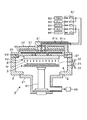
チャンバー2の上部には支持部材2aが設けられており、この支持部材2aを介してステージ3に対向するようにシャワーヘッド4が設けられている。図2はシャワーヘッド4の縦断面図であり、この図を参照しながらシャワーヘッド4の構成について説明する。シャワーヘッド4は、ベース部41、スペーサ部51及びシャワープレート42により構成されており、ベース部41の中央下面部にはスペーサ部51が設けられ、またスペーサ部51の下面側にはシャワープレート42が設けられている。図中40は、スペーサ部51及びシャワープレート42をベース部41に固着するためのねじであり、図中40aはねじ穴である。
A
ベース部41は偏平な円形状に形成されており、その下端の外側にはフランジ部が設けられ、このフランジ部が前記支持部材2aに支持される。ベース部41の内部には互いに区画された第1のガス流路41a及び第2のガス流路41bが夫々形成されている。またベース部41の上側部にはその上側部の温度を検出する検出部であるセンサ4Aが設けられており、この温度検出センサ4Aは、検出した温度に対応する電気信号を後述する制御部100に送信する。なおこの温度検出センサ4Aにより検出される温度はシャワーヘッド4において処理空間Sに面する表面の温度に対応する。
The
図3、図4はスペーサ部51の上面側、下面側の構造を夫々示したものである。スペーサ部51は、円板部52とその円板部52の周縁において上下に夫々突き出した突縁部53、54とを有しており、突縁部53の上面は前記ベース部41に、突縁部54の下面はシャワープレート42に夫々密着する。突縁部53、円板部52及びベース部41に囲まれる空間は第1のガス拡散室52aとして構成されており、また突縁部54、円板部52及びシャワープレート42に囲まれる空間は第2のガス拡散室52bとして構成されている。
3 and 4 show the structures of the upper surface side and the lower surface side of the
第1のガス拡散室52aはベース部41の第1のガス流路41aと連通している。また図3、図4では図示を省略しているが、図2に示すように円板部52の厚さ方向に沿って設けられた、区画された中間路50を介してベース部41の第2のガス供給路41bと第2のガス拡散室52bとが連通している。
The first
図3に示すように円板部52の上面側には例えば互いに間隔をおいて上方に向かう多数の柱部であるボス55が、島状に設けられており、これら各ボス55の上面(先端面)はベース部41の下面に接する。冷却部材6によりベース部41が冷却された際に各ボス55はスペーサ部51に効率良くベース部41の冷気を伝え、当該スペーサ部51の表面及びこのスペーサ部51に接続されるシャワープレート42の表面の温度を高精度に制御する役割を有する。例えばこのスペーサ部51の直径は340mmであり、このスペーサ部51においてベース部41に接する面積の合計は例えば385cm2程度である。この合計面積はスペーサ部51のベース部41への投影領域の面積の約42%である。
As shown in FIG. 3, on the upper surface side of the
図4に示すように円板部52の下面には間隔をおいて、その下面全体に亘り、多数の突起(ボス)56が設けられており、これら各ボス56先端面はシャワープレート42の上面に接する。また各ボス56及び円板部52を厚さ方向に貫くようにガス導入孔57aが穿設されており、この第1のガス導入孔57aは、前記第1のガス拡散室52aと連通している。なお図3では図示の便宜上ガス導入孔57aは数個しか描かれていないが実際は図4のボス56に対応するように多数設けられている。また図3、図4は円板部の上面、下面を夫々模式的に示したものにすぎず、ボス55及びボス56の大きさ、各ボス間の間隔、各ボス55,56の個数は夫々適宜変更し得るものである。
As shown in FIG. 4, a large number of protrusions (bosses) 56 are provided on the lower surface of the
シャワープレート42は円板状に形成された部材であり、厚さ方向に穿設された多数のガス吐出孔を有し、前記ガス吐出孔は、例えばシャワープレート42全体に亘ってマトリクス状に配列されている。これらのガス吐出孔は、第1のガス拡散室52aに連通する第1のガス吐出孔42a及び第2のガス拡散室52bに連通する第2のガス吐出孔42bにより構成されており、第1及び第2のガス吐出孔42a、42bは夫々交互に配列されている。
The
第1のガス流路41aに供給されたガスは、第1のガス拡散室52a及びガス導入孔57aを介してガス吐出口42aからシャワー状に処理空間Sに吐出され、ステージ3上のウエハWに供給される。また第2のガス流路41bに供給されたガスは、中間路50、第2のガス拡散室52bを介してガス吐出口42bからシャワー状に処理空間Sに吐出され、ステージ3上のウエハWに供給される。これら第1及び第2のガス流路41a、41bに供給された各ガスはシャワーヘッド4内では互いに混合されない。
The gas supplied to the first
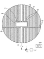
図5はベース部41の上部の構成を示した斜視図であり、この図に示すようにベース部41上には例えばアルミニウムにより構成される冷却部材6が設けられている。図6は冷却部材6の上面図であり、冷却部材6は円板状の基部61と、その基部61の上面に起立する多数の冷却用フィン62とによって構成されており、各冷却用フィン62は基部61の接線方向に沿って夫々並行するように伸長している。基部61の中央は、後述するガス供給ブロック81の接続領域となっており、当該中央には角形の孔61aが基部61の厚さ方向に設けられている。この孔61aを介して後述のガス供給ブロック81がシャワーヘッド4に接続されている。
FIG. 5 is a perspective view showing the configuration of the upper portion of the
この図6に示すように基部61上には当該基部61の一端から中心に向かうように冷却ガス導入管63が配設されており、この冷却ガス導入管63は、基部61上をその直径に沿って伸長する冷却ガス吐出管64の中央部に接続されている。また基部61上には前記ガス供給ブロック81の接続領域を囲うように側管65が設けられ、側管65の両端は冷却ガス吐出管64に接続されている。冷却ガス吐出管64及び側管65には各冷却用フィン62間の横長の隙間に、冷却用フィン62の伸長方向に沿ってガスを吐出するためのガス吹き出し口である冷却ガス吐出孔66が各々間隔をおいて設けられており、また冷却ガス導入管63には冷却ガスとして例えばドライ・エアが貯留された冷却ガス供給源67が接続されている。図中V1はバルブであり制御部100の電気信号を受けて冷却ガス供給源67から冷却ガス導入管63への冷却ガスの給断を制御する。
As shown in FIG. 6, a cooling
制御部100の電気信号を受けてバルブV1が開かれると、図7に示すように所定の流量の冷却ガスが、冷却ガス供給源67から冷却ガス導入管63を介して冷却ガス吐出管64及び側管65に流入し、冷却ガス吐出孔66から吐出される。吐出された冷却ガスは、図中矢印で示すように冷却用フィン62に沿って冷却部材6の周縁部へと向かい、冷却用フィン62及び基部61の表面がこの冷却ガスの気流に曝されて冷却される。このように冷却部材6が冷却されると、隣接するシャワーヘッド4が冷却される。なお冷却部材6、冷却ガス導入管63、冷却ガス吐出管64、側管65及び冷却ガス供給源67は特許請求の範囲でいう冷却手段を構成し、また冷却ガス導入管63、冷却ガス吐出管64及び側管65は冷却用ガス供給路を構成する。
When the valve V1 is opened in response to an electric signal from the
また図8に示すように冷却用フィン62の上部にはアルミニウムからなる板状部材70を介してシャワーへッド用加熱手段である円板状のシャワーへッド用ヒータ71が設けられており、このヒータ71は、板状部材70及び冷却部材6を介してシャワーヘッド4を加熱する。シャワーへッド用ヒータ71は、発熱抵抗体72を上下から絶縁材であるゴムシート73で挟んだ構成を有する。図中74は例えばアルミニウムからなる板状部材である。このヒータ71としては金属板に発熱抵抗体が埋め込まれたようなものを用いてもよいが、装置の軽量化を図る観点から上述のような構成にすることが好ましい。
Further, as shown in FIG. 8, a disc-shaped
シャワーヘッド4の温度検出センサ4Aから電気信号を受けた制御部100は、その温度検出センサ4Aが例えば予め設定された温度となるようにシャワーへッド用ヒータ71に電気信号を送信して、そのヒータ71の出力を調整し、ヒータ71は冷却部材6を介してシャワーヘッド4を加熱する。
Upon receiving the electrical signal from the
ヒータ71から発する熱と既述の冷却部材6の冷気とによって、シャワーヘッド4の処理空間Sに面する表面が、その表面においてTiN膜の成膜が抑えられ、かつ処理空間SにおいてウエハWに良好な成膜処理が行える温度に制御される。なお成膜処理中において前記シャワーヘッド4表面へのTiN膜の形成を防ぐためにその表面の温度は、185℃以下に制御されることが好ましい。
Due to the heat generated from the
ベース部41の上部中央にはガス供給ブロック81が設けられている。図1に示すようにガス供給ブロック81には第1のガス供給管81a、第2のガス供給管81bが設けられている。第1のガス供給管81aの一端は第1のガス流路41aに接続されており、その他端は分岐して第1の処理ガスであるNH3ガス及びキャリアガスであるN2(窒素)ガスが夫々貯留されたガス供給源82,83に接続されている。
A
また第2のガス供給管81bの一端は第2のガス流路41bに接続されており、その他端は分岐して第2の処理ガスであるTiCl4ガス、キャリアガスであるN2ガス及びクリーニングガスであるClF3ガスが夫々貯留されたガス供給源84,85,86に接続されている。また各ガス供給管81a,81bにはバルブ及びマスフローコントローラなどにより構成されるガス供給機器群87が介設されており、このガス供給機器群87は後述の制御部100からの制御信号を受信して各処理ガスの給断を制御する。なお各ガス供給源82〜86、各ガス供給管81a,81b、ガス供給機器群87は特許請求の範囲でいうガス供給機構を構成する。
One end of the second
図9は成膜装置1の上面を示した斜視図であり、この図に示すようにチャンバー2上には板部材2bを介して、冷却部材6及びヒータ71を収納するように筺体であるカバー27が設けられている。図1中27aはこのカバー27に囲まれる排気空間であり、カバー27の上部にはこの排気空間27aに向けて開口した排気口28aが設けられている。排気口28aには排気管29の一端が接続されており、排気管29の他端は排気手段29aに接続されている。
FIG. 9 is a perspective view showing the upper surface of the
吐出孔66から吐出された冷却ガスは、冷却部材6を冷却した後、排気手段29aによって排気空間27aを介して排気管29に流入して除去される。
The cooling gas discharged from the
この成膜装置1には例えばコンピュータからなる制御部100が設けられている。制御部100はプログラム、メモリ、CPUからなるデータ処理部などを備えており、前記プログラムには制御部100が成膜装置1の各部に制御信号を送り、後述の作用を実施することでウエハWに対してTiN膜が成膜できるように命令が組まれている。また、例えばメモリには処理圧力、処理時間、ガス流量、電力値などの処理パラメータの値が書き込まれる領域を備えており、CPUがプログラムの各命令を実行する際これらの処理パラメータが読み出され、そのパラメータ値に応じた制御信号がこの成膜装置1の各部に送られることになる。
The
このプログラム(処理パラメータの入力用画面に関連するプログラムも含む)は、例えばフレキシブルディスク、コンパクトディスク、MO(光磁気ディスク)などにより構成される記憶媒体である記憶部101に格納されて制御部100にインストールされる。 This program (including a program related to a process parameter input screen) is stored in the storage unit 101 which is a storage medium constituted by, for example, a flexible disk, a compact disk, an MO (magneto-optical disk), and the like. Installed on.
次いで上述の成膜装置1の作用としてウエハW表面にTiN膜を成膜する成膜方法について図10を参照しながら説明する。先ず排気手段25によりチャンバー2内を真空引きし、ガス供給源83から不活性ガスであるN2ガスが所定の流量でチャンバー2内に供給される。またこのときヒータ32によりステージ3が所定の温度例えば600℃〜700℃程度まで加熱されると共にチャンバー2の不図示のヒータが加熱され、チャンバー2内が所定の温度に維持される。
Next, a film forming method for forming a TiN film on the surface of the wafer W as an operation of the
ヒータ32及びチャンバー2の前記不図示のヒータの昇温後、冷却ガス供給源67から冷却ガスが、冷却ガス吐出管64に例えば流量150L/minで供給され、その冷却ガスがガス吐出孔66から吐出されて冷却部材6が冷却され(ステップS1)、例えば冷却ガスの供給と略同時に、排気手段29aが作動して排気空間27aが排気される。また冷却ガスが供給されると、ガスシャワーヘッド用ヒータ71が昇温して、冷却部材6を介してシャワーヘッド4に熱が伝わり、例えば温度検出センサ4Aにより検出される温度が、例えば165℃に維持されるようにシャワーヘッド4の温度が制御される(ステップS2)。
After the heaters (not shown) in the
その後、ゲートバルブ23を開き、図示しない搬送アームによりウエハWがチャンバー2内に搬入される。そして当該搬送アームとウエハ支持ピン33との協働作業によりウエハWをステージ3の上面に載置し、ゲートバルブ23を閉にする(ステップS3)。
Thereafter, the
図11は、ウエハWにTiN膜の薄膜を形成する工程におけるガスの給断及び圧力の制御を時系列に沿って示したものである。ステージ3に載置されたウエハWが所定の温度で加熱され(ステップS4)、チャンバー2内の温度が所定の温度に維持されると共にチャンバー2内の圧力が例えば260Paに維持されると、図示するように時刻t1にて両処理ガスの供給がONになり、先ず時刻t1からt2に至るまで例えばTiCl4ガスとNH3ガスとが夫々所定の流量でチャンバー2内に供給され、これらTiCl4ガスとNH3ガスとが下記の(1)式のように反応してウエハWの表面にTiN膜が成膜される(ステップS5)。
6TiCl4+8NH3→6TiN+24HCl+N2 …(1)
FIG. 11 shows the gas supply and pressure control and the pressure control in the process of forming a thin TiN film on the wafer W in chronological order. When the wafer W placed on the
6TiCl4 + 8NH3 → 6TiN + 24HCl + N2 (1)
続いて時刻t2にてTiCl4ガス及びNH3ガスの供給を停止し、チャンバー2内に残留した未反応のガスや反応副生成物を除去する。この際には、例えばN2ガスを供給してもよい。その後TiCl4ガスの供給を停止したまま、NH3ガスの供給を所定の流量で所定時間行い(詳しくはNH3ガスに加えてそのキャリアガスとしてN2ガスも供給される)、ウエハW上に成膜したTiNの中に含まれる残留塩素をNH3ガスにより還元し、この還元反応によって生じた塩化物がチャンバー2内から除去される。
Subsequently, at time t2, the supply of TiCl4 gas and NH3 gas is stopped, and unreacted gas and reaction byproducts remaining in the
そしてNH3ガスの供給を停止し、当該チャンバー2内の残留NH3ガスが排気される。このとき例えばN2ガスを供給してもよい。以上で時刻t3に至った時点で1サイクルが終了する。
Then, the supply of
この後、時刻t1から当該時刻t3に至るまでに行ったのと同様のステップ群が繰り返され、それ以後このステップ群が繰り返されて例えば時刻t1〜t3までのステップが10サイクル以上、好ましくは30サイクル以上、所望のTiN膜を得られるまで繰り返される。このサイクル数については1サイクルで形成される薄膜の膜厚によって適宜調整される。 Thereafter, the same step group as that performed from time t1 to the time t3 is repeated, and thereafter, this step group is repeated. For example, the steps from time t1 to t3 are 10 cycles or more, preferably 30. The cycle is repeated until the desired TiN film is obtained. The number of cycles is appropriately adjusted depending on the thickness of the thin film formed in one cycle.
ウエハW表面へのTiN膜の形成完了後、TiCl4及びNH3の両処理ガスの供給を停止し、所定の時間チャンバー2内のパージを行い、しかる後NH3ガスをキャリアガスであるN2ガスと共にチャンバ2内に供給して、ウエハW上のTiN膜表面の窒化処理を行う。こうして所定枚数のウエハWに対して同様の工程で繰り返し成膜処理が行われる。
After the formation of the TiN film on the surface of the wafer W is completed, the supply of both processing gases of TiCl4 and NH3 is stopped, the purge in the
所定枚数のウエハWへの成膜処理後、チャンバー2内に付着した不要な成膜物を除去するため、当該チャンバー2内にClF3ガスを供給してクリーニングが行われる。
After the film formation process on the predetermined number of wafers W, cleaning is performed by supplying ClF3 gas into the
上述の成膜装置1によれば、シャワーヘッド4の上方に冷却ガスにより冷却される冷却部材6を設け、更にその上にシャワーへッド用ヒータ71を設けている。このため処理空間S側からのウエハ用ヒータ32により輻射された熱やチャンバー2の図示しない加熱手段から輻射された熱によってシャワーヘッド4の温度が昇温しすぎる場合にはシャワーヘッド4の直ぐ上に設けられた冷却部材6の冷却作用により昇温が抑えられ、そして冷却手段6の上方のシャワーヘッド用ヒータ71を補助的に活用して冷却作用が調整されるので処理空間Sに面するシャワーヘッド表面の温度が設定温度より上昇することが抑えられ、しかも設定温度に精度よくコントロールできる。従って、ウエハW間で均一性の高いTiN膜の成膜処理を行うことができる。
According to the
またシャワーヘッド4に設けられた処理ガスの第1の拡散室52aを構成するスペーサ部51の上面には、多数のボス55が設けられ、処理ガスの第2の拡散室を構成するスペーサ部51の下面には多数のボス56が設けられ、ボス55はベース部41に、ボス56はシャワープレート42に夫々接することにより、ベース部41とスペーサ部51及びシャワープレート42との間で熱伝導が効率良く行われるため、スペーサ部51及びシャワープレート42表面の温度をより高い精度で設定温度に制御することができる。
A large number of
なお冷却手段として上述の成膜装置のように冷却部材6及びガス吐出管64などを設ける代わりに、例えば内部に通気室を設けたブロックをシャワーヘッド4とヒータ71との間に設置し、当該通気室に冷却ガスを流通させるようなものであってもよく、またペルチェ素子により構成された冷却部材を用いてもよい。
Instead of providing the cooling
また例えば冷却液が通流する流路が表面に設けられたプレートを冷却手段としてシャワーヘッド4上に設けてもよいが、既述の実施形態のように冷却ガスによる冷却手段を設けた方が冷却液が通流する配管の引き回しが不要になり、成膜装置1を構成する部品のレイアウトの自由度が高くなると共に装置の大型化を抑えることができるため好ましい。また上述の実施形態において、各冷却用フィン62は起立して設けられ、各フィン62間の隙間に冷却ガスが通流される構成であるため、冷却ガスに曝される冷却部材6の表面積を大きくとることができる一方で冷却部材6の床面積を抑えることができる。従って装置の大型化をより抑えることができる。
Further, for example, a plate having a flow path through which the coolant flows may be provided on the shower head 4 as a cooling means. However, it is preferable to provide a cooling means by cooling gas as in the above-described embodiment. It is preferable because it is not necessary to route piping through which the cooling liquid flows, and the degree of freedom in layout of components constituting the
なお上述の成膜工程では処理ガスをパルス的にチャンバー2内に導入するプロセスを繰り返し行い、膜を段階的に積層させているが、処理ガスを連続的に供給するCVD成膜処理を行ってもよい。またTiCl4ガス及びNH3ガスを同時にチャンバー2内に供給するのではなく夫々交互に供給することにより処理空間Sの雰囲気をTiCl4ガスによる雰囲気と、NH3ガスによる雰囲気とに交互に多数回、切り替えて、ウエハW上にTi原子層(あるいは分子層)の形成と窒化とを交互に形成することでTiN膜を形成してもよい。
例えばシャワーヘッド4に高周波を印加し、チャンバー2内にプラズマを発生させ、そのプラズマのエネルギーとウエハ用ヒータ32の熱エネルギーとを利用してウエハWに成膜を行ってもよい。その他に上記実施の形態ではTiN膜の成膜処理を例にとって説明したが、これに限らず成膜装置1は、Ti膜など他の膜のCVD成膜処理に適用することもできる。
In the above-described film forming process, the process of introducing the processing gas into the
For example, a high frequency may be applied to the shower head 4 to generate plasma in the
また上述の成膜装置1のシャワーヘッド4と、その上方の冷却部材6及びその冷却部材6に冷却ガスを供給する各配管と、ヒータ71とからなるガス供給装置を構成してもよい。
A gas supply device including the shower head 4 of the
なお成膜装置1を含む本発明の成膜装置及びガス供給装置は、SFDのように何も温度コントロールをしなかったらシャワーヘッド4が設定温度よりも高くなってしまうプロセスを行う場合に有効である。
The film forming apparatus and the gas supply apparatus of the present invention including the
続いて本発明の効果を確認するために以下の実施例及び比較例を行った。以下の実施例においては既述の成膜装置1を用いて、比較例においては図12に示した成膜装置9を用いてウエハWに対して処理を行った。成膜装置9は成膜装置1と略同様に構成されており、図中、成膜装置1と同様の構成を有する各部については成膜装置1に対して用いた符号と同一の符号を用いている。なおこの成膜装置9に設けられる制御部の図示は省略しているが、この成膜装置9の制御部は制御部100と同様にウエハWにTiN膜が成膜されるように当該成膜装置9の各部を制御する。
Subsequently, in order to confirm the effect of the present invention, the following examples and comparative examples were performed. In the following examples, the wafer W was processed using the
成膜装置9においてはシャワーヘッド4の上方には冷却部材6及びカバー29などが設けられておらず、その代わりにヒータ91がシャワーヘッド4上に積層されている。またヒータ91上には断熱材92が積層されている。
In the
またこの成膜装置9のシャワーヘッド4はスペーサ部51の代わりに、従来のシャワーヘッドに用いられるスペーサ部93を備えており、図13はこのスペーサ部93の上面の構成を示した図である。この図に示すように円板部52の上面にはボス55が設けられておらず、その代わりに円板部52の直径方向に沿って、互いに直交する2本のリブ94が設けられている。リブ94の上面はベース部41の下面に密着する。またスペーサ部93の直径は成膜装置1のスペーサ部51の直径と同じ340mmである。スペーサ部93においてベース部41に接する面積の合計は276cm2であり、これはスペーサ部93のベース部41への投影領域の面積の約30%に相当し、スペーサ部51がベース部41に接する面積よりも小さい。
Further, the shower head 4 of the
(実施例1−1)
成膜装置1を用いて上述の実施の形態に示した手順に従ってウエハWに対してTiN膜の成膜を行った。成膜処理中のヒータ71の温度は165℃に設定し、またガス供給源67から冷却部材6に供給される冷却ガスの流量は150L/minに設定した。またシャワーヘッド4の表面に熱電対からなる温度検出センサ(TC)を取り付け、そしてステージ3のウエハ用ヒータ32の温度を変更して、前記TCにより検出されるシャワーヘッド4の温度を調べた。
(Example 1-1)
A TiN film was formed on the wafer W using the
(比較例1−1)
実施例1−1と同様の手順でステージ3のウエハ用ヒータ32の設定温度を変更して、実施例1−1と同様に、シャワーヘッド4の表面に取り付けたTCにより検出される当該シャワーヘッド4の温度を調べた。ただしシャワーヘッド4上のヒータ91の設定温度は170℃とした。
(Comparative Example 1-1)
The set temperature of the
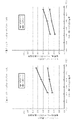
図14(a)は実施例1−1及び比較例1−1の結果を示したグラフである。このグラフに示すようにステージ3のヒータ32の温度が高く設定されると、実施例1−1に比べて比較例1−1は急激にシャワーヘッド4表面のTCにより検出される温度が高くなっている。従ってこのグラフから実施例1−1における処理空間Sに面するシャワーヘッド4の表面温度は、比較例1−1におけるシャワーヘッド4の表面温度に比べて抑えられているといえる。
FIG. 14A is a graph showing the results of Example 1-1 and Comparative Example 1-1. As shown in this graph, when the temperature of the
また実施例1−1のグラフの傾きは、比較例1−1のグラフの傾きに比べて小さいことから、実施例1−1では比較例1−1に比べてシャワーヘッド4の温度上昇が抑えられているといえる。 Moreover, since the slope of the graph of Example 1-1 is smaller than the slope of the graph of Comparative Example 1-1, the temperature rise of the shower head 4 is suppressed in Example 1-1 compared to Comparative Example 1-1. It can be said that.
(実施例1−2)
予め処理空間Sに面するシャワーヘッド4表面にTiN膜を形成(プリコート)してから既述の実施形態と同様にウエハWの処理を行った他は実施例1−1と同じく、ステージ3のヒータ32の設定温度を変更して、シャワーヘッド4表面のTCにより検出される温度を調べた。
(Example 1-2)
As in Example 1-1, the wafer W was processed in the same manner as in the above-described embodiment after the TiN film was formed (precoated) on the surface of the shower head 4 facing the processing space S in advance. The temperature detected by TC on the surface of the shower head 4 was examined by changing the set temperature of the
(比較例1−2)
実施例1−2と同様に予め処理空間Sに面するシャワーヘッド4表面にTiN膜をプリコートした他は比較例1−1と同様にステージ3のヒータ32の設定温度を変更して、シャワーヘッド4表面のTCにより検出される温度を調べた。
(Comparative Example 1-2)
Similar to Example 1-2, the set temperature of the
図14(b)は実施例1−2及び比較例1−2の結果を示したグラフである。このグラフに示すように比較例1−2に比べて実施例1−2で前記TCにより検出されるシャワーヘッド4の温度は低く、従って実施例1−2のシャワーヘッド4の表面温度は比較例1−2のシャワーヘッド4の表面温度に比べて抑えられていることが分かる。 FIG. 14B is a graph showing the results of Example 1-2 and Comparative Example 1-2. As shown in this graph, the temperature of the showerhead 4 detected by the TC in Example 1-2 is lower than that in Comparative Example 1-2. Therefore, the surface temperature of the showerhead 4 in Example 1-2 is comparative. It turns out that it is suppressed compared with the surface temperature of the shower head 4 of 1-2.
また図14(b)のグラフの600℃〜700℃付近の温度範囲において実施例1−2のグラフの傾きは比較例1−2のグラフの傾きよりも小さく、従ってこの範囲において実施例1−2では比較例1−2に比べてシャワーヘッド4の温度上昇が抑えられているといえる。 In addition, in the temperature range of 600 ° C. to 700 ° C. in the graph of FIG. 14B, the slope of the graph of Example 1-2 is smaller than the slope of the graph of Comparative Example 1-2. 2, it can be said that the temperature rise of the shower head 4 is suppressed as compared with Comparative Example 1-2.
(実施例2)
実施例2では既述の成膜装置1を用いて実施の形態に示した手順に従って500枚のウエハWに順次TiN膜を成膜し、この成膜時における温度検出センサ4Aが示すシャワーヘッド4の温度の変化と、シャワーヘッド4上のヒータ71の出力とをモニタした。なお制御部100のプログラムには成膜処理中にセンサ4Aの温度が165℃に維持されるようにヒータ71の温度が調整されるように設定されている。
(Example 2)
In Example 2, TiN films are sequentially formed on 500 wafers W according to the procedure described in the embodiment using the
(比較例2)
比較例2では既述の成膜装置9を用いて実施の形態に示した手順に従って500枚のウエハWに順次TiN膜を成膜し、この成膜時における温度検出センサ4Aの示す値の変化と、シャワーヘッド4上のヒータ92の出力とをモニタした。なおこの成膜装置9の制御部のプログラムには成膜処理中にセンサ4Aの温度が170℃に維持されるようにヒータ92の温度が調整されるように設定されている。
(Comparative Example 2)
In Comparative Example 2, TiN films are sequentially formed on 500 wafers W according to the procedure described in the embodiment using the
図15(a)は実施例2及び比較例2のモニタされた温度を示しており、実施例2では設定通りの温度165℃で推移しているのに対し、比較例2では処理開始直後に設定された温度170℃を超え、その後時間が経過するにつれて温度が上昇している。 FIG. 15A shows the monitored temperatures of Example 2 and Comparative Example 2. In Example 2, the set temperature was 165 ° C., whereas in Comparative Example 2, immediately after the start of processing. The set temperature exceeds 170 ° C., and thereafter the temperature increases as time passes.
図15(b)は実施例2のヒータ71及び比較例2のヒータ92の出力を示しており、このグラフの横軸に示す時間は、図15(a)のグラフの横軸に示す時間に対応している。このグラフに示すように実施例のヒータ71の出力は処理開始直後に90%程度に上昇した後50%に下降し、その50%周辺で安定しているが、比較例2においては開始直後から出力が低下し、略0%になっている。
FIG. 15B shows the outputs of the
従って図15(a),(b)のグラフから実施例2においては冷却部材6及びヒータ71によりシャワーヘッド4を安定して温度制御することができるため、シャワーヘッド4の処理空間Sに向かう表面の温度を制御でき、その表面においてTiN膜の成膜を抑えることができることが示された。一方、比較例2においてはヒータ71の出力がゼロになってもシャワーヘッド4の温度は上昇し続けており、そのシャワーヘッド4の温度が制御できなくなっていることが分かる。
Accordingly, in the second embodiment, the temperature of the shower head 4 can be stably controlled by the cooling
W 半導体ウエハ
1 成膜装置
2 チャンバー
3 ステージ
32 ウエハ用ヒータ
4 シャワーヘッド
6 冷却部材
71 シャワーへッド用ヒータ
Claims (23)
このチャンバー内に設けられ、基板を載置するステージと、
前記ステージに載置された基板を加熱する基板用加熱手段と、
前記ステージに対向して設けられた、多数のガス吐出孔を有するシャワーヘッドと、
このシャワーヘッドを介してチャンバー内に処理ガスを供給するガス供給機構と、
前記シャワーヘッドの上方に設けられた、シャワーヘッドを冷却する冷却手段と、
この冷却手段の上方に設けられ、当該冷却手段を介してシャワーヘッドを加熱するシャワーへッド用加熱手段と、
を備えていることを特徴とする成膜装置。 A chamber for forming a processing space for performing a film forming process on the substrate;
A stage provided in the chamber and on which a substrate is placed;
Substrate heating means for heating the substrate placed on the stage;
A shower head having a large number of gas discharge holes provided opposite to the stage;
A gas supply mechanism for supplying a processing gas into the chamber via the shower head;
Cooling means provided above the shower head for cooling the shower head;
A heating means for a shower head that is provided above the cooling means and heats the shower head via the cooling means;
A film forming apparatus comprising:
この冷却用フィンに冷却用ガスを供給する冷却用ガス供給路と、を備えていることを特徴とする請求項1記載の成膜装置。 The cooling means includes a cooling fin,
The film forming apparatus according to claim 1, further comprising: a cooling gas supply path that supplies a cooling gas to the cooling fin.
前記ステージに対向して設けられるシャワーヘッドと、
前記シャワーヘッドの上方に設けられた、シャワーヘッドを冷却する冷却手段と、
この冷却手段の上方に設けられ、当該冷却手段を介してシャワーヘッドを加熱するシャワーへッド用加熱手段と、
を備えたことを特徴とするガス供給装置。 In a gas supply apparatus for supplying a processing gas to a substrate placed on a stage in a chamber,
A shower head provided facing the stage;
Cooling means provided above the shower head for cooling the shower head;
A heating means for a shower head that is provided above the cooling means and heats the shower head via the cooling means;
A gas supply device comprising:
この冷却用フィンに冷却用ガスを供給する冷却用ガス供給路と、を備えていることを特徴とする請求項9に記載のガス供給装置。 The cooling means includes a cooling fin,
The gas supply device according to claim 9, further comprising a cooling gas supply path that supplies a cooling gas to the cooling fin.
基板をステージに載置する工程と、
基板を基板用加熱手段により加熱する工程と、
ガス供給機構によりシャワーヘッドを介して処理空間に処理ガスを供給する工程と、
シャワーヘッドの上方に設けられた冷却手段によりシャワーヘッドを冷却する工程と、
前記冷却手段の上方に設けられた、シャワーヘッド用加熱手段により当該冷却手段を介してシャワーヘッドを加熱する工程と、
を含むことを特徴とする成膜方法。 A chamber for forming a processing space for performing a film forming process on the substrate; a stage provided in the chamber for mounting the substrate; a substrate heating means for heating the substrate mounted on the stage; and the stage About a method of forming a film on a substrate using a film forming apparatus provided with a shower head having a large number of gas discharge holes provided facing each other.
Placing the substrate on the stage;
Heating the substrate by the substrate heating means;
Supplying a processing gas to the processing space via a shower head by a gas supply mechanism;
Cooling the shower head by cooling means provided above the shower head;
A step of heating the shower head via the cooling means by the heating means for the shower head provided above the cooling means;
A film forming method comprising:
その温度検出部の温度検出値に基づいてシャワーへッド用加熱手段を制御する工程と、
を備えたことを特徴とする請求項15ないし19のいずれか一に記載の成膜方法。 Detecting the temperature corresponding to the lower surface of the shower head by the temperature detector;
Controlling the shower head heating means based on the temperature detection value of the temperature detection unit;
The film forming method according to claim 15, further comprising:
The film forming method according to claim 21, wherein the first processing gas is a titanium compound, and the second processing gas is ammonia gas.
請求項15ないし22のいずれか一に記載の成膜方法を実施するためのステップ群を含んだコンピュータプログラムを備えたことを特徴とする記憶媒体。
A chamber for forming a processing space for performing a film forming process on the substrate; a stage provided in the chamber for mounting the substrate; a substrate heating means for heating the substrate mounted on the stage; and the stage In a storage medium provided with a computer program for performing a method of forming a film on a substrate using a film forming apparatus provided with a shower head having a large number of gas discharge holes provided facing each other,
23. A storage medium comprising a computer program including a group of steps for performing the film forming method according to claim 15.
Priority Applications (6)
| Application Number | Priority Date | Filing Date | Title |
|---|---|---|---|
| JP2006170585A JP5045000B2 (en) | 2006-06-20 | 2006-06-20 | Film forming apparatus, gas supply apparatus, film forming method, and storage medium |
| CN2007800020357A CN101365823B (en) | 2006-06-20 | 2007-06-19 | Film forming apparatus and film forming method |
| PCT/JP2007/062328 WO2007148692A1 (en) | 2006-06-20 | 2007-06-19 | Film forming apparatus and film forming method |
| KR1020087030964A KR101089977B1 (en) | 2006-06-20 | 2007-06-19 | Film forming apparatus and method, gas supply device and storage medium |
| TW096122094A TWI427679B (en) | 2006-06-20 | 2007-06-20 | Film forming apparatus and film forming method |
| US12/340,058 US8133323B2 (en) | 2006-06-20 | 2008-12-19 | Film forming apparatus and method, gas supply device and storage medium |
Applications Claiming Priority (1)
| Application Number | Priority Date | Filing Date | Title |
|---|---|---|---|
| JP2006170585A JP5045000B2 (en) | 2006-06-20 | 2006-06-20 | Film forming apparatus, gas supply apparatus, film forming method, and storage medium |
Publications (3)
| Publication Number | Publication Date |
|---|---|
| JP2008001923A JP2008001923A (en) | 2008-01-10 |
| JP2008001923A5 JP2008001923A5 (en) | 2009-07-02 |
| JP5045000B2 true JP5045000B2 (en) | 2012-10-10 |
Family
ID=38833434
Family Applications (1)
| Application Number | Title | Priority Date | Filing Date |
|---|---|---|---|
| JP2006170585A Active JP5045000B2 (en) | 2006-06-20 | 2006-06-20 | Film forming apparatus, gas supply apparatus, film forming method, and storage medium |
Country Status (6)
| Country | Link |
|---|---|
| US (1) | US8133323B2 (en) |
| JP (1) | JP5045000B2 (en) |
| KR (1) | KR101089977B1 (en) |
| CN (1) | CN101365823B (en) |
| TW (1) | TWI427679B (en) |
| WO (1) | WO2007148692A1 (en) |
Families Citing this family (361)
| Publication number | Priority date | Publication date | Assignee | Title |
|---|---|---|---|---|
| JP5202050B2 (en) * | 2008-03-14 | 2013-06-05 | 東京エレクトロン株式会社 | Shower head and substrate processing apparatus |
| FR2930561B1 (en) * | 2008-04-28 | 2011-01-14 | Altatech Semiconductor | DEVICE AND METHOD FOR CHEMICAL TREATMENT IN STEAM PHASE. |
| US20110070370A1 (en) | 2008-05-28 | 2011-03-24 | Aixtron Ag | Thermal gradient enhanced chemical vapour deposition (tge-cvd) |
| WO2009144456A1 (en) * | 2008-05-28 | 2009-12-03 | Aixtron Ag | Thermal gradient enhanced chemical vapour deposition (tge-cvd) |
| JP2010016225A (en) * | 2008-07-04 | 2010-01-21 | Tokyo Electron Ltd | Thermal control mechanism and semiconductor manufacturing device using the same |
| JP5231117B2 (en) * | 2008-07-24 | 2013-07-10 | 株式会社ニューフレアテクノロジー | Film forming apparatus and film forming method |
| JP5106331B2 (en) | 2008-09-16 | 2012-12-26 | 東京エレクトロン株式会社 | Method for lowering temperature of substrate mounting table, computer-readable storage medium, and substrate processing system |
| US10378106B2 (en) | 2008-11-14 | 2019-08-13 | Asm Ip Holding B.V. | Method of forming insulation film by modified PEALD |
| US8931431B2 (en) * | 2009-03-25 | 2015-01-13 | The Regents Of The University Of Michigan | Nozzle geometry for organic vapor jet printing |
| US9394608B2 (en) | 2009-04-06 | 2016-07-19 | Asm America, Inc. | Semiconductor processing reactor and components thereof |
| US8802201B2 (en) | 2009-08-14 | 2014-08-12 | Asm America, Inc. | Systems and methods for thin-film deposition of metal oxides using excited nitrogen-oxygen species |
| KR101108879B1 (en) * | 2009-08-31 | 2012-01-30 | 주식회사 원익아이피에스 | Gas injecting device and Substrate processing apparatus using the same |
| US20110061810A1 (en) * | 2009-09-11 | 2011-03-17 | Applied Materials, Inc. | Apparatus and Methods for Cyclical Oxidation and Etching |
| US20110065276A1 (en) * | 2009-09-11 | 2011-03-17 | Applied Materials, Inc. | Apparatus and Methods for Cyclical Oxidation and Etching |
| US20110061812A1 (en) * | 2009-09-11 | 2011-03-17 | Applied Materials, Inc. | Apparatus and Methods for Cyclical Oxidation and Etching |
| JP5323628B2 (en) * | 2009-09-17 | 2013-10-23 | 東京エレクトロン株式会社 | Plasma processing equipment |
| WO2011044451A2 (en) * | 2009-10-09 | 2011-04-14 | Applied Materials, Inc. | Multi-gas centrally cooled showerhead design |
| JP2011168881A (en) * | 2010-01-25 | 2011-09-01 | Hitachi Kokusai Electric Inc | Method of manufacturing semiconductor device and substrate processing apparatus |
| JP5409413B2 (en) * | 2010-01-26 | 2014-02-05 | 日本パイオニクス株式会社 | III-nitride semiconductor vapor phase growth system |
| US9441295B2 (en) * | 2010-05-14 | 2016-09-13 | Solarcity Corporation | Multi-channel gas-delivery system |
| JP5982758B2 (en) * | 2011-02-23 | 2016-08-31 | 東京エレクトロン株式会社 | Microwave irradiation device |
| US20120225203A1 (en) * | 2011-03-01 | 2012-09-06 | Applied Materials, Inc. | Apparatus and Process for Atomic Layer Deposition |
| US9312155B2 (en) | 2011-06-06 | 2016-04-12 | Asm Japan K.K. | High-throughput semiconductor-processing apparatus equipped with multiple dual-chamber modules |
| US10364496B2 (en) | 2011-06-27 | 2019-07-30 | Asm Ip Holding B.V. | Dual section module having shared and unshared mass flow controllers |
| US10854498B2 (en) | 2011-07-15 | 2020-12-01 | Asm Ip Holding B.V. | Wafer-supporting device and method for producing same |
| US20130023129A1 (en) | 2011-07-20 | 2013-01-24 | Asm America, Inc. | Pressure transmitter for a semiconductor processing environment |
| CN103014668B (en) * | 2011-09-23 | 2014-12-24 | 理想能源设备(上海)有限公司 | Chemical vapor deposition (CVD) device |
| CN103014669B (en) * | 2011-09-23 | 2014-11-26 | 理想能源设备(上海)有限公司 | Chemical vapor deposition (CVD) device |
| CN103014665B (en) * | 2011-09-23 | 2015-02-18 | 理想能源设备(上海)有限公司 | Chemical vapor deposition apparatus for metallorganic compounds and gas conveying method thereof |
| CN103014666B (en) * | 2011-09-23 | 2014-11-26 | 理想能源设备(上海)有限公司 | Chemical vapor deposition (CVD) device |
| CN103014667B (en) * | 2011-09-23 | 2015-07-01 | 理想能源设备(上海)有限公司 | Chemical vapor deposition (CVD) device |
| US9017481B1 (en) | 2011-10-28 | 2015-04-28 | Asm America, Inc. | Process feed management for semiconductor substrate processing |
| JP6038618B2 (en) * | 2011-12-15 | 2016-12-07 | 株式会社ニューフレアテクノロジー | Film forming apparatus and film forming method |
| KR101327458B1 (en) * | 2012-01-10 | 2013-11-08 | 주식회사 유진테크 | Showerhead having cooling system and substrate processing apparatus including the showerhead |
| CN103388132B (en) * | 2012-05-11 | 2015-11-25 | 中微半导体设备(上海)有限公司 | Gas spray, its manufacture method and film growth reactor |
| US9659799B2 (en) | 2012-08-28 | 2017-05-23 | Asm Ip Holding B.V. | Systems and methods for dynamic semiconductor process scheduling |
| US9021985B2 (en) | 2012-09-12 | 2015-05-05 | Asm Ip Holdings B.V. | Process gas management for an inductively-coupled plasma deposition reactor |
| US9132436B2 (en) * | 2012-09-21 | 2015-09-15 | Applied Materials, Inc. | Chemical control features in wafer process equipment |
| US10714315B2 (en) * | 2012-10-12 | 2020-07-14 | Asm Ip Holdings B.V. | Semiconductor reaction chamber showerhead |
| US20160376700A1 (en) | 2013-02-01 | 2016-12-29 | Asm Ip Holding B.V. | System for treatment of deposition reactor |
| KR102231596B1 (en) * | 2013-02-06 | 2021-03-25 | 어플라이드 머티어리얼스, 인코포레이티드 | Gas injection apparatus and substrate process chamber incorporating same |
| US9589770B2 (en) | 2013-03-08 | 2017-03-07 | Asm Ip Holding B.V. | Method and systems for in-situ formation of intermediate reactive species |
| US9484191B2 (en) | 2013-03-08 | 2016-11-01 | Asm Ip Holding B.V. | Pulsed remote plasma method and system |
| JP2013110440A (en) * | 2013-03-11 | 2013-06-06 | Tokyo Electron Ltd | Electrode unit and substrate processing apparatus |
| TWI627305B (en) * | 2013-03-15 | 2018-06-21 | 應用材料股份有限公司 | Atmospheric lid with rigid plate for carousel processing chambers |
| JP2014192372A (en) * | 2013-03-27 | 2014-10-06 | Tokyo Electron Ltd | Microwave heating apparatus |
| KR101467195B1 (en) * | 2013-05-14 | 2014-12-01 | 주식회사 아바코 | Gas sprayer and thin film depositing apparatus having the same |
| KR101526505B1 (en) * | 2013-06-20 | 2015-06-09 | 피에스케이 주식회사 | Unit and method for cooling, and apparatus and method for treating substrate |
| JP6180208B2 (en) * | 2013-07-08 | 2017-08-16 | 株式会社ニューフレアテクノロジー | Vapor growth apparatus and vapor growth method |
| US9240412B2 (en) | 2013-09-27 | 2016-01-19 | Asm Ip Holding B.V. | Semiconductor structure and device and methods of forming same using selective epitaxial process |
| KR20150055227A (en) * | 2013-11-13 | 2015-05-21 | 삼성전자주식회사 | Showerhead and apparatus for processing a substrate including the same |
| JP6135475B2 (en) * | 2013-11-20 | 2017-05-31 | 東京エレクトロン株式会社 | Gas supply apparatus, film forming apparatus, gas supply method, and storage medium |
| JP5971870B2 (en) | 2013-11-29 | 2016-08-17 | 株式会社日立国際電気 | Substrate processing apparatus, semiconductor device manufacturing method, and recording medium |
| JP5726281B1 (en) * | 2013-12-27 | 2015-05-27 | 株式会社日立国際電気 | Substrate processing apparatus and semiconductor device manufacturing method |
| JP6123688B2 (en) * | 2014-01-29 | 2017-05-10 | 東京エレクトロン株式会社 | Deposition equipment |
| US10683571B2 (en) | 2014-02-25 | 2020-06-16 | Asm Ip Holding B.V. | Gas supply manifold and method of supplying gases to chamber using same |
| US10167557B2 (en) | 2014-03-18 | 2019-01-01 | Asm Ip Holding B.V. | Gas distribution system, reactor including the system, and methods of using the same |
| US11015245B2 (en) | 2014-03-19 | 2021-05-25 | Asm Ip Holding B.V. | Gas-phase reactor and system having exhaust plenum and components thereof |
| FR3018825B1 (en) * | 2014-03-21 | 2017-09-01 | Altatech Semiconductor | GAS PHASE DEPOSITION METHOD |
| KR102386812B1 (en) * | 2014-05-16 | 2022-04-15 | 어플라이드 머티어리얼스, 인코포레이티드 | Showerhead design |
| US9911579B2 (en) * | 2014-07-03 | 2018-03-06 | Applied Materials, Inc. | Showerhead having a detachable high resistivity gas distribution plate |
| US10858737B2 (en) | 2014-07-28 | 2020-12-08 | Asm Ip Holding B.V. | Showerhead assembly and components thereof |
| US9890456B2 (en) | 2014-08-21 | 2018-02-13 | Asm Ip Holding B.V. | Method and system for in situ formation of gas-phase compounds |
| US10407771B2 (en) * | 2014-10-06 | 2019-09-10 | Applied Materials, Inc. | Atomic layer deposition chamber with thermal lid |
| US9657845B2 (en) | 2014-10-07 | 2017-05-23 | Asm Ip Holding B.V. | Variable conductance gas distribution apparatus and method |
| US10941490B2 (en) | 2014-10-07 | 2021-03-09 | Asm Ip Holding B.V. | Multiple temperature range susceptor, assembly, reactor and system including the susceptor, and methods of using the same |
| KR102263121B1 (en) | 2014-12-22 | 2021-06-09 | 에이에스엠 아이피 홀딩 비.브이. | Semiconductor device and manufacuring method thereof |
| US10529542B2 (en) | 2015-03-11 | 2020-01-07 | Asm Ip Holdings B.V. | Cross-flow reactor and method |
| US10276355B2 (en) | 2015-03-12 | 2019-04-30 | Asm Ip Holding B.V. | Multi-zone reactor, system including the reactor, and method of using the same |
| JP6193284B2 (en) * | 2015-03-18 | 2017-09-06 | 株式会社東芝 | Channel structure, intake / exhaust member, and processing apparatus |
| CN104789943A (en) * | 2015-04-01 | 2015-07-22 | 沈阳拓荆科技有限公司 | Temperature-controllable double-gas channel spraying plate with uniform gas spraying function |
| US20160359080A1 (en) | 2015-06-07 | 2016-12-08 | Solarcity Corporation | System, method and apparatus for chemical vapor deposition |
| US10458018B2 (en) | 2015-06-26 | 2019-10-29 | Asm Ip Holding B.V. | Structures including metal carbide material, devices including the structures, and methods of forming same |
| US10600673B2 (en) | 2015-07-07 | 2020-03-24 | Asm Ip Holding B.V. | Magnetic susceptor to baseplate seal |
| US10083836B2 (en) | 2015-07-24 | 2018-09-25 | Asm Ip Holding B.V. | Formation of boron-doped titanium metal films with high work function |
| US11421321B2 (en) | 2015-07-28 | 2022-08-23 | Asm Ip Holding B.V. | Apparatuses for thin film deposition |
| US20170029948A1 (en) * | 2015-07-28 | 2017-02-02 | Asm Ip Holding B.V. | Methods and apparatuses for temperature-indexed thin film deposition |
| US10204790B2 (en) | 2015-07-28 | 2019-02-12 | Asm Ip Holding B.V. | Methods for thin film deposition |
| US9960072B2 (en) | 2015-09-29 | 2018-05-01 | Asm Ip Holding B.V. | Variable adjustment for precise matching of multiple chamber cavity housings |
| US10211308B2 (en) | 2015-10-21 | 2019-02-19 | Asm Ip Holding B.V. | NbMC layers |
| US10322384B2 (en) | 2015-11-09 | 2019-06-18 | Asm Ip Holding B.V. | Counter flow mixer for process chamber |
| US11139308B2 (en) | 2015-12-29 | 2021-10-05 | Asm Ip Holding B.V. | Atomic layer deposition of III-V compounds to form V-NAND devices |
| US10468251B2 (en) | 2016-02-19 | 2019-11-05 | Asm Ip Holding B.V. | Method for forming spacers using silicon nitride film for spacer-defined multiple patterning |
| US10529554B2 (en) | 2016-02-19 | 2020-01-07 | Asm Ip Holding B.V. | Method for forming silicon nitride film selectively on sidewalls or flat surfaces of trenches |
| US10501866B2 (en) | 2016-03-09 | 2019-12-10 | Asm Ip Holding B.V. | Gas distribution apparatus for improved film uniformity in an epitaxial system |
| US10343920B2 (en) | 2016-03-18 | 2019-07-09 | Asm Ip Holding B.V. | Aligned carbon nanotubes |
| US9892913B2 (en) | 2016-03-24 | 2018-02-13 | Asm Ip Holding B.V. | Radial and thickness control via biased multi-port injection settings |
| US10190213B2 (en) | 2016-04-21 | 2019-01-29 | Asm Ip Holding B.V. | Deposition of metal borides |
| US10865475B2 (en) | 2016-04-21 | 2020-12-15 | Asm Ip Holding B.V. | Deposition of metal borides and silicides |
| US10032628B2 (en) | 2016-05-02 | 2018-07-24 | Asm Ip Holding B.V. | Source/drain performance through conformal solid state doping |
| US10367080B2 (en) | 2016-05-02 | 2019-07-30 | Asm Ip Holding B.V. | Method of forming a germanium oxynitride film |
| KR102592471B1 (en) | 2016-05-17 | 2023-10-20 | 에이에스엠 아이피 홀딩 비.브이. | Method of forming metal interconnection and method of fabricating semiconductor device using the same |
| US9748434B1 (en) | 2016-05-24 | 2017-08-29 | Tesla, Inc. | Systems, method and apparatus for curing conductive paste |
| US11453943B2 (en) | 2016-05-25 | 2022-09-27 | Asm Ip Holding B.V. | Method for forming carbon-containing silicon/metal oxide or nitride film by ALD using silicon precursor and hydrocarbon precursor |
| EP3255173B1 (en) * | 2016-06-06 | 2018-11-21 | Meyer Burger (Germany) AG | Layered gas distributor with temperature-controlled fluid |
| JP6696322B2 (en) * | 2016-06-24 | 2020-05-20 | 東京エレクトロン株式会社 | Gas processing apparatus, gas processing method and storage medium |
| US10388509B2 (en) | 2016-06-28 | 2019-08-20 | Asm Ip Holding B.V. | Formation of epitaxial layers via dislocation filtering |
| US9859151B1 (en) | 2016-07-08 | 2018-01-02 | Asm Ip Holding B.V. | Selective film deposition method to form air gaps |
| US10612137B2 (en) | 2016-07-08 | 2020-04-07 | Asm Ip Holdings B.V. | Organic reactants for atomic layer deposition |
| US10714385B2 (en) | 2016-07-19 | 2020-07-14 | Asm Ip Holding B.V. | Selective deposition of tungsten |
| KR102354490B1 (en) | 2016-07-27 | 2022-01-21 | 에이에스엠 아이피 홀딩 비.브이. | Method of processing a substrate |
| US9887082B1 (en) | 2016-07-28 | 2018-02-06 | Asm Ip Holding B.V. | Method and apparatus for filling a gap |
| US10395919B2 (en) | 2016-07-28 | 2019-08-27 | Asm Ip Holding B.V. | Method and apparatus for filling a gap |
| KR102532607B1 (en) | 2016-07-28 | 2023-05-15 | 에이에스엠 아이피 홀딩 비.브이. | Substrate processing apparatus and method of operating the same |
| US9812320B1 (en) | 2016-07-28 | 2017-11-07 | Asm Ip Holding B.V. | Method and apparatus for filling a gap |
| US9954136B2 (en) | 2016-08-03 | 2018-04-24 | Tesla, Inc. | Cassette optimized for an inline annealing system |
| US10410943B2 (en) | 2016-10-13 | 2019-09-10 | Asm Ip Holding B.V. | Method for passivating a surface of a semiconductor and related systems |
| US10643826B2 (en) | 2016-10-26 | 2020-05-05 | Asm Ip Holdings B.V. | Methods for thermally calibrating reaction chambers |
| US11532757B2 (en) | 2016-10-27 | 2022-12-20 | Asm Ip Holding B.V. | Deposition of charge trapping layers |
| US10115856B2 (en) | 2016-10-31 | 2018-10-30 | Tesla, Inc. | System and method for curing conductive paste using induction heating |
| US10229833B2 (en) | 2016-11-01 | 2019-03-12 | Asm Ip Holding B.V. | Methods for forming a transition metal nitride film on a substrate by atomic layer deposition and related semiconductor device structures |
| US10435790B2 (en) | 2016-11-01 | 2019-10-08 | Asm Ip Holding B.V. | Method of subatmospheric plasma-enhanced ALD using capacitively coupled electrodes with narrow gap |
| US10643904B2 (en) | 2016-11-01 | 2020-05-05 | Asm Ip Holdings B.V. | Methods for forming a semiconductor device and related semiconductor device structures |
| US10714350B2 (en) | 2016-11-01 | 2020-07-14 | ASM IP Holdings, B.V. | Methods for forming a transition metal niobium nitride film on a substrate by atomic layer deposition and related semiconductor device structures |
| WO2018083989A1 (en) * | 2016-11-02 | 2018-05-11 | 東京エレクトロン株式会社 | Shower head and substrate processing device |
| US10134757B2 (en) | 2016-11-07 | 2018-11-20 | Asm Ip Holding B.V. | Method of processing a substrate and a device manufactured by using the method |
| KR102546317B1 (en) | 2016-11-15 | 2023-06-21 | 에이에스엠 아이피 홀딩 비.브이. | Gas supply unit and substrate processing apparatus including the same |
| US10340135B2 (en) | 2016-11-28 | 2019-07-02 | Asm Ip Holding B.V. | Method of topologically restricted plasma-enhanced cyclic deposition of silicon or metal nitride |
| KR20180068582A (en) | 2016-12-14 | 2018-06-22 | 에이에스엠 아이피 홀딩 비.브이. | Substrate processing apparatus |
| US11447861B2 (en) | 2016-12-15 | 2022-09-20 | Asm Ip Holding B.V. | Sequential infiltration synthesis apparatus and a method of forming a patterned structure |
| US11581186B2 (en) | 2016-12-15 | 2023-02-14 | Asm Ip Holding B.V. | Sequential infiltration synthesis apparatus |
| KR20180070971A (en) | 2016-12-19 | 2018-06-27 | 에이에스엠 아이피 홀딩 비.브이. | Substrate processing apparatus |
| US10269558B2 (en) | 2016-12-22 | 2019-04-23 | Asm Ip Holding B.V. | Method of forming a structure on a substrate |
| US10867788B2 (en) | 2016-12-28 | 2020-12-15 | Asm Ip Holding B.V. | Method of forming a structure on a substrate |
| US10655221B2 (en) | 2017-02-09 | 2020-05-19 | Asm Ip Holding B.V. | Method for depositing oxide film by thermal ALD and PEALD |
| US10468261B2 (en) | 2017-02-15 | 2019-11-05 | Asm Ip Holding B.V. | Methods for forming a metallic film on a substrate by cyclical deposition and related semiconductor device structures |
| US10529563B2 (en) | 2017-03-29 | 2020-01-07 | Asm Ip Holdings B.V. | Method for forming doped metal oxide films on a substrate by cyclical deposition and related semiconductor device structures |
| US10283353B2 (en) | 2017-03-29 | 2019-05-07 | Asm Ip Holding B.V. | Method of reforming insulating film deposited on substrate with recess pattern |
| KR102096700B1 (en) * | 2017-03-29 | 2020-04-02 | 도쿄엘렉트론가부시키가이샤 | Substrate processing apparatus and substrate procesing method |
| KR102457289B1 (en) | 2017-04-25 | 2022-10-21 | 에이에스엠 아이피 홀딩 비.브이. | Method for depositing a thin film and manufacturing a semiconductor device |
| US10446393B2 (en) | 2017-05-08 | 2019-10-15 | Asm Ip Holding B.V. | Methods for forming silicon-containing epitaxial layers and related semiconductor device structures |
| US10770286B2 (en) | 2017-05-08 | 2020-09-08 | Asm Ip Holdings B.V. | Methods for selectively forming a silicon nitride film on a substrate and related semiconductor device structures |
| US10892156B2 (en) | 2017-05-08 | 2021-01-12 | Asm Ip Holding B.V. | Methods for forming a silicon nitride film on a substrate and related semiconductor device structures |
| US10504742B2 (en) | 2017-05-31 | 2019-12-10 | Asm Ip Holding B.V. | Method of atomic layer etching using hydrogen plasma |
| US10886123B2 (en) | 2017-06-02 | 2021-01-05 | Asm Ip Holding B.V. | Methods for forming low temperature semiconductor layers and related semiconductor device structures |
| US11306395B2 (en) | 2017-06-28 | 2022-04-19 | Asm Ip Holding B.V. | Methods for depositing a transition metal nitride film on a substrate by atomic layer deposition and related deposition apparatus |
| US10685834B2 (en) | 2017-07-05 | 2020-06-16 | Asm Ip Holdings B.V. | Methods for forming a silicon germanium tin layer and related semiconductor device structures |
| KR20190009245A (en) | 2017-07-18 | 2019-01-28 | 에이에스엠 아이피 홀딩 비.브이. | Methods for forming a semiconductor device structure and related semiconductor device structures |
| US10541333B2 (en) | 2017-07-19 | 2020-01-21 | Asm Ip Holding B.V. | Method for depositing a group IV semiconductor and related semiconductor device structures |
| US11018002B2 (en) | 2017-07-19 | 2021-05-25 | Asm Ip Holding B.V. | Method for selectively depositing a Group IV semiconductor and related semiconductor device structures |
| US11374112B2 (en) | 2017-07-19 | 2022-06-28 | Asm Ip Holding B.V. | Method for depositing a group IV semiconductor and related semiconductor device structures |
| US10312055B2 (en) | 2017-07-26 | 2019-06-04 | Asm Ip Holding B.V. | Method of depositing film by PEALD using negative bias |
| US10590535B2 (en) | 2017-07-26 | 2020-03-17 | Asm Ip Holdings B.V. | Chemical treatment, deposition and/or infiltration apparatus and method for using the same |
| US10605530B2 (en) | 2017-07-26 | 2020-03-31 | Asm Ip Holding B.V. | Assembly of a liner and a flange for a vertical furnace as well as the liner and the vertical furnace |
| US10692741B2 (en) | 2017-08-08 | 2020-06-23 | Asm Ip Holdings B.V. | Radiation shield |
| US10770336B2 (en) | 2017-08-08 | 2020-09-08 | Asm Ip Holding B.V. | Substrate lift mechanism and reactor including same |
| US11769682B2 (en) | 2017-08-09 | 2023-09-26 | Asm Ip Holding B.V. | Storage apparatus for storing cassettes for substrates and processing apparatus equipped therewith |
| US11139191B2 (en) | 2017-08-09 | 2021-10-05 | Asm Ip Holding B.V. | Storage apparatus for storing cassettes for substrates and processing apparatus equipped therewith |
| US10249524B2 (en) | 2017-08-09 | 2019-04-02 | Asm Ip Holding B.V. | Cassette holder assembly for a substrate cassette and holding member for use in such assembly |
| US10236177B1 (en) | 2017-08-22 | 2019-03-19 | ASM IP Holding B.V.. | Methods for depositing a doped germanium tin semiconductor and related semiconductor device structures |
| USD900036S1 (en) | 2017-08-24 | 2020-10-27 | Asm Ip Holding B.V. | Heater electrical connector and adapter |
| US11830730B2 (en) | 2017-08-29 | 2023-11-28 | Asm Ip Holding B.V. | Layer forming method and apparatus |
| US11295980B2 (en) | 2017-08-30 | 2022-04-05 | Asm Ip Holding B.V. | Methods for depositing a molybdenum metal film over a dielectric surface of a substrate by a cyclical deposition process and related semiconductor device structures |
| KR102491945B1 (en) | 2017-08-30 | 2023-01-26 | 에이에스엠 아이피 홀딩 비.브이. | Substrate processing apparatus |
| US11056344B2 (en) | 2017-08-30 | 2021-07-06 | Asm Ip Holding B.V. | Layer forming method |
| US10607895B2 (en) | 2017-09-18 | 2020-03-31 | Asm Ip Holdings B.V. | Method for forming a semiconductor device structure comprising a gate fill metal |
| KR102630301B1 (en) | 2017-09-21 | 2024-01-29 | 에이에스엠 아이피 홀딩 비.브이. | Method of sequential infiltration synthesis treatment of infiltrateable material and structures and devices formed using same |
| US10844484B2 (en) | 2017-09-22 | 2020-11-24 | Asm Ip Holding B.V. | Apparatus for dispensing a vapor phase reactant to a reaction chamber and related methods |
| US10658205B2 (en) | 2017-09-28 | 2020-05-19 | Asm Ip Holdings B.V. | Chemical dispensing apparatus and methods for dispensing a chemical to a reaction chamber |
| US10403504B2 (en) | 2017-10-05 | 2019-09-03 | Asm Ip Holding B.V. | Method for selectively depositing a metallic film on a substrate |
| US10319588B2 (en) | 2017-10-10 | 2019-06-11 | Asm Ip Holding B.V. | Method for depositing a metal chalcogenide on a substrate by cyclical deposition |
| US10923344B2 (en) | 2017-10-30 | 2021-02-16 | Asm Ip Holding B.V. | Methods for forming a semiconductor structure and related semiconductor structures |
| US10910262B2 (en) | 2017-11-16 | 2021-02-02 | Asm Ip Holding B.V. | Method of selectively depositing a capping layer structure on a semiconductor device structure |
| KR102443047B1 (en) | 2017-11-16 | 2022-09-14 | 에이에스엠 아이피 홀딩 비.브이. | Method of processing a substrate and a device manufactured by the same |
| US11022879B2 (en) | 2017-11-24 | 2021-06-01 | Asm Ip Holding B.V. | Method of forming an enhanced unexposed photoresist layer |
| KR102597978B1 (en) | 2017-11-27 | 2023-11-06 | 에이에스엠 아이피 홀딩 비.브이. | Storage device for storing wafer cassettes for use with batch furnaces |
| US11639811B2 (en) | 2017-11-27 | 2023-05-02 | Asm Ip Holding B.V. | Apparatus including a clean mini environment |
| US10290508B1 (en) | 2017-12-05 | 2019-05-14 | Asm Ip Holding B.V. | Method for forming vertical spacers for spacer-defined patterning |
| US10872771B2 (en) | 2018-01-16 | 2020-12-22 | Asm Ip Holding B. V. | Method for depositing a material film on a substrate within a reaction chamber by a cyclical deposition process and related device structures |
| US11482412B2 (en) | 2018-01-19 | 2022-10-25 | Asm Ip Holding B.V. | Method for depositing a gap-fill layer by plasma-assisted deposition |
| TW202325889A (en) | 2018-01-19 | 2023-07-01 | 荷蘭商Asm 智慧財產控股公司 | Deposition method |
| USD903477S1 (en) | 2018-01-24 | 2020-12-01 | Asm Ip Holdings B.V. | Metal clamp |
| US11018047B2 (en) | 2018-01-25 | 2021-05-25 | Asm Ip Holding B.V. | Hybrid lift pin |
| USD880437S1 (en) | 2018-02-01 | 2020-04-07 | Asm Ip Holding B.V. | Gas supply plate for semiconductor manufacturing apparatus |
| US10535516B2 (en) | 2018-02-01 | 2020-01-14 | Asm Ip Holdings B.V. | Method for depositing a semiconductor structure on a surface of a substrate and related semiconductor structures |
| US11081345B2 (en) | 2018-02-06 | 2021-08-03 | Asm Ip Holding B.V. | Method of post-deposition treatment for silicon oxide film |
| US10896820B2 (en) | 2018-02-14 | 2021-01-19 | Asm Ip Holding B.V. | Method for depositing a ruthenium-containing film on a substrate by a cyclical deposition process |
| WO2019158960A1 (en) | 2018-02-14 | 2019-08-22 | Asm Ip Holding B.V. | A method for depositing a ruthenium-containing film on a substrate by a cyclical deposition process |
| US10731249B2 (en) | 2018-02-15 | 2020-08-04 | Asm Ip Holding B.V. | Method of forming a transition metal containing film on a substrate by a cyclical deposition process, a method for supplying a transition metal halide compound to a reaction chamber, and related vapor deposition apparatus |
| KR102636427B1 (en) | 2018-02-20 | 2024-02-13 | 에이에스엠 아이피 홀딩 비.브이. | Substrate processing method and apparatus |
| US10658181B2 (en) | 2018-02-20 | 2020-05-19 | Asm Ip Holding B.V. | Method of spacer-defined direct patterning in semiconductor fabrication |
| US10975470B2 (en) | 2018-02-23 | 2021-04-13 | Asm Ip Holding B.V. | Apparatus for detecting or monitoring for a chemical precursor in a high temperature environment |
| US11473195B2 (en) | 2018-03-01 | 2022-10-18 | Asm Ip Holding B.V. | Semiconductor processing apparatus and a method for processing a substrate |
| US11629406B2 (en) | 2018-03-09 | 2023-04-18 | Asm Ip Holding B.V. | Semiconductor processing apparatus comprising one or more pyrometers for measuring a temperature of a substrate during transfer of the substrate |
| US11114283B2 (en) | 2018-03-16 | 2021-09-07 | Asm Ip Holding B.V. | Reactor, system including the reactor, and methods of manufacturing and using same |
| KR102646467B1 (en) | 2018-03-27 | 2024-03-11 | 에이에스엠 아이피 홀딩 비.브이. | Method of forming an electrode on a substrate and a semiconductor device structure including an electrode |
| US11230766B2 (en) | 2018-03-29 | 2022-01-25 | Asm Ip Holding B.V. | Substrate processing apparatus and method |
| US11088002B2 (en) | 2018-03-29 | 2021-08-10 | Asm Ip Holding B.V. | Substrate rack and a substrate processing system and method |
| US10510536B2 (en) | 2018-03-29 | 2019-12-17 | Asm Ip Holding B.V. | Method of depositing a co-doped polysilicon film on a surface of a substrate within a reaction chamber |
| KR102501472B1 (en) | 2018-03-30 | 2023-02-20 | 에이에스엠 아이피 홀딩 비.브이. | Substrate processing method |
| JP7093667B2 (en) * | 2018-04-11 | 2022-06-30 | 東京エレクトロン株式会社 | Film forming equipment and film forming method |
| TWI811348B (en) | 2018-05-08 | 2023-08-11 | 荷蘭商Asm 智慧財產控股公司 | Methods for depositing an oxide film on a substrate by a cyclical deposition process and related device structures |
| TWI816783B (en) | 2018-05-11 | 2023-10-01 | 荷蘭商Asm 智慧財產控股公司 | Methods for forming a doped metal carbide film on a substrate and related semiconductor device structures |
| KR102596988B1 (en) | 2018-05-28 | 2023-10-31 | 에이에스엠 아이피 홀딩 비.브이. | Method of processing a substrate and a device manufactured by the same |
| US11270899B2 (en) | 2018-06-04 | 2022-03-08 | Asm Ip Holding B.V. | Wafer handling chamber with moisture reduction |
| US11718913B2 (en) | 2018-06-04 | 2023-08-08 | Asm Ip Holding B.V. | Gas distribution system and reactor system including same |
| US11286562B2 (en) | 2018-06-08 | 2022-03-29 | Asm Ip Holding B.V. | Gas-phase chemical reactor and method of using same |
| KR102568797B1 (en) | 2018-06-21 | 2023-08-21 | 에이에스엠 아이피 홀딩 비.브이. | Substrate processing system |
| US10797133B2 (en) | 2018-06-21 | 2020-10-06 | Asm Ip Holding B.V. | Method for depositing a phosphorus doped silicon arsenide film and related semiconductor device structures |
| CN112292477A (en) | 2018-06-27 | 2021-01-29 | Asm Ip私人控股有限公司 | Cyclic deposition methods for forming metal-containing materials and films and structures containing metal-containing materials |
| JP2021529254A (en) | 2018-06-27 | 2021-10-28 | エーエスエム・アイピー・ホールディング・ベー・フェー | Periodic deposition methods for forming metal-containing materials and films and structures containing metal-containing materials |
| KR20200002519A (en) | 2018-06-29 | 2020-01-08 | 에이에스엠 아이피 홀딩 비.브이. | Method for depositing a thin film and manufacturing a semiconductor device |
| US10612136B2 (en) | 2018-06-29 | 2020-04-07 | ASM IP Holding, B.V. | Temperature-controlled flange and reactor system including same |
| US10388513B1 (en) | 2018-07-03 | 2019-08-20 | Asm Ip Holding B.V. | Method for depositing silicon-free carbon-containing film as gap-fill layer by pulse plasma-assisted deposition |
| US10755922B2 (en) | 2018-07-03 | 2020-08-25 | Asm Ip Holding B.V. | Method for depositing silicon-free carbon-containing film as gap-fill layer by pulse plasma-assisted deposition |
| US10767789B2 (en) | 2018-07-16 | 2020-09-08 | Asm Ip Holding B.V. | Diaphragm valves, valve components, and methods for forming valve components |
| US10483099B1 (en) | 2018-07-26 | 2019-11-19 | Asm Ip Holding B.V. | Method for forming thermally stable organosilicon polymer film |
| US11053591B2 (en) | 2018-08-06 | 2021-07-06 | Asm Ip Holding B.V. | Multi-port gas injection system and reactor system including same |
| JP6715894B2 (en) * | 2018-08-07 | 2020-07-01 | 株式会社Kokusai Electric | Semiconductor device manufacturing method, substrate processing apparatus, and program |
| US10883175B2 (en) | 2018-08-09 | 2021-01-05 | Asm Ip Holding B.V. | Vertical furnace for processing substrates and a liner for use therein |
| US10829852B2 (en) | 2018-08-16 | 2020-11-10 | Asm Ip Holding B.V. | Gas distribution device for a wafer processing apparatus |
| US11430674B2 (en) | 2018-08-22 | 2022-08-30 | Asm Ip Holding B.V. | Sensor array, apparatus for dispensing a vapor phase reactant to a reaction chamber and related methods |
| US11024523B2 (en) | 2018-09-11 | 2021-06-01 | Asm Ip Holding B.V. | Substrate processing apparatus and method |
| KR20200030162A (en) | 2018-09-11 | 2020-03-20 | 에이에스엠 아이피 홀딩 비.브이. | Method for deposition of a thin film |
| US11049751B2 (en) | 2018-09-14 | 2021-06-29 | Asm Ip Holding B.V. | Cassette supply system to store and handle cassettes and processing apparatus equipped therewith |
| CN110970344A (en) | 2018-10-01 | 2020-04-07 | Asm Ip控股有限公司 | Substrate holding apparatus, system including the same, and method of using the same |
| US11232963B2 (en) | 2018-10-03 | 2022-01-25 | Asm Ip Holding B.V. | Substrate processing apparatus and method |
| KR102592699B1 (en) | 2018-10-08 | 2023-10-23 | 에이에스엠 아이피 홀딩 비.브이. | Substrate support unit and apparatuses for depositing thin film and processing the substrate including the same |
| US10847365B2 (en) | 2018-10-11 | 2020-11-24 | Asm Ip Holding B.V. | Method of forming conformal silicon carbide film by cyclic CVD |
| US10811256B2 (en) | 2018-10-16 | 2020-10-20 | Asm Ip Holding B.V. | Method for etching a carbon-containing feature |
| KR102546322B1 (en) | 2018-10-19 | 2023-06-21 | 에이에스엠 아이피 홀딩 비.브이. | Substrate processing apparatus and substrate processing method |
| KR102605121B1 (en) | 2018-10-19 | 2023-11-23 | 에이에스엠 아이피 홀딩 비.브이. | Substrate processing apparatus and substrate processing method |
| USD948463S1 (en) | 2018-10-24 | 2022-04-12 | Asm Ip Holding B.V. | Susceptor for semiconductor substrate supporting apparatus |
| US10381219B1 (en) | 2018-10-25 | 2019-08-13 | Asm Ip Holding B.V. | Methods for forming a silicon nitride film |
| US11087997B2 (en) | 2018-10-31 | 2021-08-10 | Asm Ip Holding B.V. | Substrate processing apparatus for processing substrates |
| KR20200051105A (en) | 2018-11-02 | 2020-05-13 | 에이에스엠 아이피 홀딩 비.브이. | Substrate support unit and substrate processing apparatus including the same |
| US11572620B2 (en) | 2018-11-06 | 2023-02-07 | Asm Ip Holding B.V. | Methods for selectively depositing an amorphous silicon film on a substrate |
| US11031242B2 (en) | 2018-11-07 | 2021-06-08 | Asm Ip Holding B.V. | Methods for depositing a boron doped silicon germanium film |
| US10847366B2 (en) | 2018-11-16 | 2020-11-24 | Asm Ip Holding B.V. | Methods for depositing a transition metal chalcogenide film on a substrate by a cyclical deposition process |
| US10818758B2 (en) | 2018-11-16 | 2020-10-27 | Asm Ip Holding B.V. | Methods for forming a metal silicate film on a substrate in a reaction chamber and related semiconductor device structures |
| US10559458B1 (en) | 2018-11-26 | 2020-02-11 | Asm Ip Holding B.V. | Method of forming oxynitride film |
| US11217444B2 (en) | 2018-11-30 | 2022-01-04 | Asm Ip Holding B.V. | Method for forming an ultraviolet radiation responsive metal oxide-containing film |
| KR102636428B1 (en) | 2018-12-04 | 2024-02-13 | 에이에스엠 아이피 홀딩 비.브이. | A method for cleaning a substrate processing apparatus |
| US11158513B2 (en) | 2018-12-13 | 2021-10-26 | Asm Ip Holding B.V. | Methods for forming a rhenium-containing film on a substrate by a cyclical deposition process and related semiconductor device structures |
| JP2020096183A (en) | 2018-12-14 | 2020-06-18 | エーエスエム・アイピー・ホールディング・ベー・フェー | Method of forming device structure using selective deposition of gallium nitride, and system for the same |
| JP7224175B2 (en) * | 2018-12-26 | 2023-02-17 | 東京エレクトロン株式会社 | Deposition apparatus and method |
| TWI819180B (en) | 2019-01-17 | 2023-10-21 | 荷蘭商Asm 智慧財產控股公司 | Methods of forming a transition metal containing film on a substrate by a cyclical deposition process |
| KR20200091543A (en) | 2019-01-22 | 2020-07-31 | 에이에스엠 아이피 홀딩 비.브이. | Semiconductor processing device |
| CN111524788B (en) | 2019-02-01 | 2023-11-24 | Asm Ip私人控股有限公司 | Method for topologically selective film formation of silicon oxide |
| US11482533B2 (en) | 2019-02-20 | 2022-10-25 | Asm Ip Holding B.V. | Apparatus and methods for plug fill deposition in 3-D NAND applications |
| KR102626263B1 (en) | 2019-02-20 | 2024-01-16 | 에이에스엠 아이피 홀딩 비.브이. | Cyclical deposition method including treatment step and apparatus for same |
| JP2020136677A (en) | 2019-02-20 | 2020-08-31 | エーエスエム・アイピー・ホールディング・ベー・フェー | Periodic accumulation method for filing concave part formed inside front surface of base material, and device |
| KR102638425B1 (en) | 2019-02-20 | 2024-02-21 | 에이에스엠 아이피 홀딩 비.브이. | Method and apparatus for filling a recess formed within a substrate surface |
| JP2020133004A (en) | 2019-02-22 | 2020-08-31 | エーエスエム・アイピー・ホールディング・ベー・フェー | Base material processing apparatus and method for processing base material |
| KR20200108243A (en) | 2019-03-08 | 2020-09-17 | 에이에스엠 아이피 홀딩 비.브이. | Structure Including SiOC Layer and Method of Forming Same |
| US11742198B2 (en) | 2019-03-08 | 2023-08-29 | Asm Ip Holding B.V. | Structure including SiOCN layer and method of forming same |
| KR20200108242A (en) | 2019-03-08 | 2020-09-17 | 에이에스엠 아이피 홀딩 비.브이. | Method for Selective Deposition of Silicon Nitride Layer and Structure Including Selectively-Deposited Silicon Nitride Layer |
| KR20210127768A (en) * | 2019-03-11 | 2021-10-22 | 어플라이드 머티어리얼스, 인코포레이티드 | Lid assembly apparatus and methods for substrate processing chambers |
| JP2020167398A (en) | 2019-03-28 | 2020-10-08 | エーエスエム・アイピー・ホールディング・ベー・フェー | Door opener and substrate processing apparatus provided therewith |
| KR20200116855A (en) | 2019-04-01 | 2020-10-13 | 에이에스엠 아이피 홀딩 비.브이. | Method of manufacturing semiconductor device |
| US11447864B2 (en) | 2019-04-19 | 2022-09-20 | Asm Ip Holding B.V. | Layer forming method and apparatus |
| KR20200125453A (en) | 2019-04-24 | 2020-11-04 | 에이에스엠 아이피 홀딩 비.브이. | Gas-phase reactor system and method of using same |
| KR20200130118A (en) | 2019-05-07 | 2020-11-18 | 에이에스엠 아이피 홀딩 비.브이. | Method for Reforming Amorphous Carbon Polymer Film |
| KR20200130121A (en) | 2019-05-07 | 2020-11-18 | 에이에스엠 아이피 홀딩 비.브이. | Chemical source vessel with dip tube |
| KR20200130652A (en) | 2019-05-10 | 2020-11-19 | 에이에스엠 아이피 홀딩 비.브이. | Method of depositing material onto a surface and structure formed according to the method |
| JP2020188255A (en) | 2019-05-16 | 2020-11-19 | エーエスエム アイピー ホールディング ビー.ブイ. | Wafer boat handling device, vertical batch furnace, and method |
| USD947913S1 (en) | 2019-05-17 | 2022-04-05 | Asm Ip Holding B.V. | Susceptor shaft |
| USD975665S1 (en) | 2019-05-17 | 2023-01-17 | Asm Ip Holding B.V. | Susceptor shaft |
| USD935572S1 (en) | 2019-05-24 | 2021-11-09 | Asm Ip Holding B.V. | Gas channel plate |
| USD922229S1 (en) | 2019-06-05 | 2021-06-15 | Asm Ip Holding B.V. | Device for controlling a temperature of a gas supply unit |
| KR20200141002A (en) | 2019-06-06 | 2020-12-17 | 에이에스엠 아이피 홀딩 비.브이. | Method of using a gas-phase reactor system including analyzing exhausted gas |
| KR20200143254A (en) | 2019-06-11 | 2020-12-23 | 에이에스엠 아이피 홀딩 비.브이. | Method of forming an electronic structure using an reforming gas, system for performing the method, and structure formed using the method |
| USD944946S1 (en) | 2019-06-14 | 2022-03-01 | Asm Ip Holding B.V. | Shower plate |
| USD931978S1 (en) | 2019-06-27 | 2021-09-28 | Asm Ip Holding B.V. | Showerhead vacuum transport |
| KR20210005515A (en) | 2019-07-03 | 2021-01-14 | 에이에스엠 아이피 홀딩 비.브이. | Temperature control assembly for substrate processing apparatus and method of using same |
| KR102268559B1 (en) * | 2019-07-03 | 2021-06-22 | 세메스 주식회사 | Shower head unit and system for treating substrate with the shower head unit |
| JP2021015791A (en) | 2019-07-09 | 2021-02-12 | エーエスエム アイピー ホールディング ビー.ブイ. | Plasma device and substrate processing method using coaxial waveguide |
| CN112216646A (en) | 2019-07-10 | 2021-01-12 | Asm Ip私人控股有限公司 | Substrate supporting assembly and substrate processing device comprising same |
| KR20210010307A (en) | 2019-07-16 | 2021-01-27 | 에이에스엠 아이피 홀딩 비.브이. | Substrate processing apparatus |
| KR20210010816A (en) | 2019-07-17 | 2021-01-28 | 에이에스엠 아이피 홀딩 비.브이. | Radical assist ignition plasma system and method |
| KR20210010820A (en) | 2019-07-17 | 2021-01-28 | 에이에스엠 아이피 홀딩 비.브이. | Methods of forming silicon germanium structures |
| US11643724B2 (en) | 2019-07-18 | 2023-05-09 | Asm Ip Holding B.V. | Method of forming structures using a neutral beam |
| CN112242296A (en) | 2019-07-19 | 2021-01-19 | Asm Ip私人控股有限公司 | Method of forming topologically controlled amorphous carbon polymer films |
| TW202113936A (en) | 2019-07-29 | 2021-04-01 | 荷蘭商Asm Ip私人控股有限公司 | Methods for selective deposition utilizing n-type dopants and/or alternative dopants to achieve high dopant incorporation |
| CN112309899A (en) | 2019-07-30 | 2021-02-02 | Asm Ip私人控股有限公司 | Substrate processing apparatus |
| CN112309900A (en) | 2019-07-30 | 2021-02-02 | Asm Ip私人控股有限公司 | Substrate processing apparatus |
| US11227782B2 (en) | 2019-07-31 | 2022-01-18 | Asm Ip Holding B.V. | Vertical batch furnace assembly |
| US11587815B2 (en) | 2019-07-31 | 2023-02-21 | Asm Ip Holding B.V. | Vertical batch furnace assembly |
| US11587814B2 (en) | 2019-07-31 | 2023-02-21 | Asm Ip Holding B.V. | Vertical batch furnace assembly |
| CN112323048B (en) | 2019-08-05 | 2024-02-09 | Asm Ip私人控股有限公司 | Liquid level sensor for chemical source container |
| USD965044S1 (en) | 2019-08-19 | 2022-09-27 | Asm Ip Holding B.V. | Susceptor shaft |
| USD965524S1 (en) | 2019-08-19 | 2022-10-04 | Asm Ip Holding B.V. | Susceptor support |
| JP2021031769A (en) | 2019-08-21 | 2021-03-01 | エーエスエム アイピー ホールディング ビー.ブイ. | Production apparatus of mixed gas of film deposition raw material and film deposition apparatus |
| USD949319S1 (en) | 2019-08-22 | 2022-04-19 | Asm Ip Holding B.V. | Exhaust duct |
| USD979506S1 (en) | 2019-08-22 | 2023-02-28 | Asm Ip Holding B.V. | Insulator |
| USD930782S1 (en) | 2019-08-22 | 2021-09-14 | Asm Ip Holding B.V. | Gas distributor |
| USD940837S1 (en) | 2019-08-22 | 2022-01-11 | Asm Ip Holding B.V. | Electrode |
| KR20210024423A (en) | 2019-08-22 | 2021-03-05 | 에이에스엠 아이피 홀딩 비.브이. | Method for forming a structure with a hole |
| US11286558B2 (en) | 2019-08-23 | 2022-03-29 | Asm Ip Holding B.V. | Methods for depositing a molybdenum nitride film on a surface of a substrate by a cyclical deposition process and related semiconductor device structures including a molybdenum nitride film |
| KR20210024420A (en) | 2019-08-23 | 2021-03-05 | 에이에스엠 아이피 홀딩 비.브이. | Method for depositing silicon oxide film having improved quality by peald using bis(diethylamino)silane |
| KR20210029090A (en) | 2019-09-04 | 2021-03-15 | 에이에스엠 아이피 홀딩 비.브이. | Methods for selective deposition using a sacrificial capping layer |
| KR20210029663A (en) | 2019-09-05 | 2021-03-16 | 에이에스엠 아이피 홀딩 비.브이. | Substrate processing apparatus |
| US11562901B2 (en) | 2019-09-25 | 2023-01-24 | Asm Ip Holding B.V. | Substrate processing method |
| CN112593212B (en) | 2019-10-02 | 2023-12-22 | Asm Ip私人控股有限公司 | Method for forming topologically selective silicon oxide film by cyclic plasma enhanced deposition process |
| TW202129060A (en) | 2019-10-08 | 2021-08-01 | 荷蘭商Asm Ip控股公司 | Substrate processing device, and substrate processing method |
| TW202115273A (en) | 2019-10-10 | 2021-04-16 | 荷蘭商Asm Ip私人控股有限公司 | Method of forming a photoresist underlayer and structure including same |
| KR20210045930A (en) | 2019-10-16 | 2021-04-27 | 에이에스엠 아이피 홀딩 비.브이. | Method of Topology-Selective Film Formation of Silicon Oxide |
| US11637014B2 (en) | 2019-10-17 | 2023-04-25 | Asm Ip Holding B.V. | Methods for selective deposition of doped semiconductor material |
| KR20210047808A (en) | 2019-10-21 | 2021-04-30 | 에이에스엠 아이피 홀딩 비.브이. | Apparatus and methods for selectively etching films |
| US11646205B2 (en) | 2019-10-29 | 2023-05-09 | Asm Ip Holding B.V. | Methods of selectively forming n-type doped material on a surface, systems for selectively forming n-type doped material, and structures formed using same |
| KR20210054983A (en) | 2019-11-05 | 2021-05-14 | 에이에스엠 아이피 홀딩 비.브이. | Structures with doped semiconductor layers and methods and systems for forming same |
| US11501968B2 (en) | 2019-11-15 | 2022-11-15 | Asm Ip Holding B.V. | Method for providing a semiconductor device with silicon filled gaps |
| KR20210062561A (en) | 2019-11-20 | 2021-05-31 | 에이에스엠 아이피 홀딩 비.브이. | Method of depositing carbon-containing material on a surface of a substrate, structure formed using the method, and system for forming the structure |
| CN112951697A (en) | 2019-11-26 | 2021-06-11 | Asm Ip私人控股有限公司 | Substrate processing apparatus |
| US11450529B2 (en) | 2019-11-26 | 2022-09-20 | Asm Ip Holding B.V. | Methods for selectively forming a target film on a substrate comprising a first dielectric surface and a second metallic surface |
| CN112885693A (en) | 2019-11-29 | 2021-06-01 | Asm Ip私人控股有限公司 | Substrate processing apparatus |
| CN112885692A (en) | 2019-11-29 | 2021-06-01 | Asm Ip私人控股有限公司 | Substrate processing apparatus |
| JP2021090042A (en) | 2019-12-02 | 2021-06-10 | エーエスエム アイピー ホールディング ビー.ブイ. | Substrate processing apparatus and substrate processing method |
| KR20210070898A (en) | 2019-12-04 | 2021-06-15 | 에이에스엠 아이피 홀딩 비.브이. | Substrate processing apparatus |
| JP2021097227A (en) | 2019-12-17 | 2021-06-24 | エーエスエム・アイピー・ホールディング・ベー・フェー | Method of forming vanadium nitride layer and structure including vanadium nitride layer |
| US11527403B2 (en) | 2019-12-19 | 2022-12-13 | Asm Ip Holding B.V. | Methods for filling a gap feature on a substrate surface and related semiconductor structures |
| JP2021109175A (en) | 2020-01-06 | 2021-08-02 | エーエスエム・アイピー・ホールディング・ベー・フェー | Gas supply assembly, components thereof, and reactor system including the same |
| KR20210095050A (en) | 2020-01-20 | 2021-07-30 | 에이에스엠 아이피 홀딩 비.브이. | Method of forming thin film and method of modifying surface of thin film |
| TW202130846A (en) | 2020-02-03 | 2021-08-16 | 荷蘭商Asm Ip私人控股有限公司 | Method of forming structures including a vanadium or indium layer |
| TW202146882A (en) | 2020-02-04 | 2021-12-16 | 荷蘭商Asm Ip私人控股有限公司 | Method of verifying an article, apparatus for verifying an article, and system for verifying a reaction chamber |
| US11776846B2 (en) | 2020-02-07 | 2023-10-03 | Asm Ip Holding B.V. | Methods for depositing gap filling fluids and related systems and devices |
| US11781243B2 (en) | 2020-02-17 | 2023-10-10 | Asm Ip Holding B.V. | Method for depositing low temperature phosphorous-doped silicon |
| TW202203344A (en) | 2020-02-28 | 2022-01-16 | 荷蘭商Asm Ip控股公司 | System dedicated for parts cleaning |
| KR20210116240A (en) | 2020-03-11 | 2021-09-27 | 에이에스엠 아이피 홀딩 비.브이. | Substrate handling device with adjustable joints |
| US11876356B2 (en) | 2020-03-11 | 2024-01-16 | Asm Ip Holding B.V. | Lockout tagout assembly and system and method of using same |
| CN113394086A (en) | 2020-03-12 | 2021-09-14 | Asm Ip私人控股有限公司 | Method for producing a layer structure having a target topological profile |
| KR20210124042A (en) | 2020-04-02 | 2021-10-14 | 에이에스엠 아이피 홀딩 비.브이. | Thin film forming method |
| TW202146689A (en) | 2020-04-03 | 2021-12-16 | 荷蘭商Asm Ip控股公司 | Method for forming barrier layer and method for manufacturing semiconductor device |
| TW202145344A (en) | 2020-04-08 | 2021-12-01 | 荷蘭商Asm Ip私人控股有限公司 | Apparatus and methods for selectively etching silcon oxide films |
| US11821078B2 (en) | 2020-04-15 | 2023-11-21 | Asm Ip Holding B.V. | Method for forming precoat film and method for forming silicon-containing film |
| CN113555279A (en) | 2020-04-24 | 2021-10-26 | Asm Ip私人控股有限公司 | Method of forming vanadium nitride-containing layers and structures including the same |
| KR20210132600A (en) | 2020-04-24 | 2021-11-04 | 에이에스엠 아이피 홀딩 비.브이. | Methods and systems for depositing a layer comprising vanadium, nitrogen, and a further element |
| TW202146831A (en) | 2020-04-24 | 2021-12-16 | 荷蘭商Asm Ip私人控股有限公司 | Vertical batch furnace assembly, and method for cooling vertical batch furnace |
| KR20210134226A (en) | 2020-04-29 | 2021-11-09 | 에이에스엠 아이피 홀딩 비.브이. | Solid source precursor vessel |
| KR20210134869A (en) | 2020-05-01 | 2021-11-11 | 에이에스엠 아이피 홀딩 비.브이. | Fast FOUP swapping with a FOUP handler |
| KR20210141379A (en) | 2020-05-13 | 2021-11-23 | 에이에스엠 아이피 홀딩 비.브이. | Laser alignment fixture for a reactor system |
| TW202147383A (en) | 2020-05-19 | 2021-12-16 | 荷蘭商Asm Ip私人控股有限公司 | Substrate processing apparatus |
| KR20210145078A (en) | 2020-05-21 | 2021-12-01 | 에이에스엠 아이피 홀딩 비.브이. | Structures including multiple carbon layers and methods of forming and using same |
| KR20210145080A (en) | 2020-05-22 | 2021-12-01 | 에이에스엠 아이피 홀딩 비.브이. | Apparatus for depositing thin films using hydrogen peroxide |
| TW202201602A (en) | 2020-05-29 | 2022-01-01 | 荷蘭商Asm Ip私人控股有限公司 | Substrate processing device |
| TW202218133A (en) | 2020-06-24 | 2022-05-01 | 荷蘭商Asm Ip私人控股有限公司 | Method for forming a layer provided with silicon |
| TW202217953A (en) | 2020-06-30 | 2022-05-01 | 荷蘭商Asm Ip私人控股有限公司 | Substrate processing method |
| KR20220010438A (en) | 2020-07-17 | 2022-01-25 | 에이에스엠 아이피 홀딩 비.브이. | Structures and methods for use in photolithography |
| TW202204662A (en) | 2020-07-20 | 2022-02-01 | 荷蘭商Asm Ip私人控股有限公司 | Method and system for depositing molybdenum layers |
| TW202212623A (en) | 2020-08-26 | 2022-04-01 | 荷蘭商Asm Ip私人控股有限公司 | Method of forming metal silicon oxide layer and metal silicon oxynitride layer, semiconductor structure, and system |
| USD990534S1 (en) | 2020-09-11 | 2023-06-27 | Asm Ip Holding B.V. | Weighted lift pin |
| US20220093361A1 (en) * | 2020-09-22 | 2022-03-24 | Applied Materials, Inc. | Showerhead assembly with recursive gas channels |
| USD1012873S1 (en) | 2020-09-24 | 2024-01-30 | Asm Ip Holding B.V. | Electrode for semiconductor processing apparatus |
| CN116194616A (en) * | 2020-09-25 | 2023-05-30 | 朗姆研究公司 | Axial cooling metal spray head for high-temperature process |
| TW202229613A (en) | 2020-10-14 | 2022-08-01 | 荷蘭商Asm Ip私人控股有限公司 | Method of depositing material on stepped structure |
| TW202217037A (en) | 2020-10-22 | 2022-05-01 | 荷蘭商Asm Ip私人控股有限公司 | Method of depositing vanadium metal, structure, device and a deposition assembly |
| TW202223136A (en) | 2020-10-28 | 2022-06-16 | 荷蘭商Asm Ip私人控股有限公司 | Method for forming layer on substrate, and semiconductor processing system |
| KR20220076343A (en) | 2020-11-30 | 2022-06-08 | 에이에스엠 아이피 홀딩 비.브이. | an injector configured for arrangement within a reaction chamber of a substrate processing apparatus |
| US11946137B2 (en) | 2020-12-16 | 2024-04-02 | Asm Ip Holding B.V. | Runout and wobble measurement fixtures |
| TW202231903A (en) | 2020-12-22 | 2022-08-16 | 荷蘭商Asm Ip私人控股有限公司 | Transition metal deposition method, transition metal layer, and deposition assembly for depositing transition metal on substrate |
| US11705312B2 (en) * | 2020-12-26 | 2023-07-18 | Applied Materials, Inc. | Vertically adjustable plasma source |
| JP7114763B1 (en) * | 2021-02-15 | 2022-08-08 | 株式会社Kokusai Electric | Semiconductor device manufacturing method, substrate processing apparatus, program, and substrate processing method |
| CN113136568B (en) * | 2021-04-07 | 2022-10-11 | 拓荆科技股份有限公司 | Energy-saving type active temperature control spray head |
| USD980813S1 (en) | 2021-05-11 | 2023-03-14 | Asm Ip Holding B.V. | Gas flow control plate for substrate processing apparatus |
| USD1023959S1 (en) | 2021-05-11 | 2024-04-23 | Asm Ip Holding B.V. | Electrode for substrate processing apparatus |
| USD981973S1 (en) | 2021-05-11 | 2023-03-28 | Asm Ip Holding B.V. | Reactor wall for substrate processing apparatus |
| USD980814S1 (en) | 2021-05-11 | 2023-03-14 | Asm Ip Holding B.V. | Gas distributor for substrate processing apparatus |
| WO2023283375A1 (en) * | 2021-07-08 | 2023-01-12 | Applied Materials, Inc. | Showerhead assembly with recursive gas channels |
| USD990441S1 (en) | 2021-09-07 | 2023-06-27 | Asm Ip Holding B.V. | Gas flow control plate |
| WO2023054531A1 (en) * | 2021-09-29 | 2023-04-06 | 京セラ株式会社 | Shower plate |
| EP4190938B1 (en) * | 2021-12-03 | 2024-03-06 | Semsysco GmbH | Distribution body for distributing a process gas for treating a substrate by means of the process gas |
Family Cites Families (32)
| Publication number | Priority date | Publication date | Assignee | Title |
|---|---|---|---|---|
| US4590042A (en) * | 1984-12-24 | 1986-05-20 | Tegal Corporation | Plasma reactor having slotted manifold |
| US4793975A (en) * | 1985-05-20 | 1988-12-27 | Tegal Corporation | Plasma Reactor with removable insert |
| JP2747036B2 (en) * | 1989-07-07 | 1998-05-06 | 日本電信電話株式会社 | Thin film formation method |
| DE4011933C2 (en) * | 1990-04-12 | 1996-11-21 | Balzers Hochvakuum | Process for the reactive surface treatment of a workpiece and treatment chamber therefor |
| US5647945A (en) * | 1993-08-25 | 1997-07-15 | Tokyo Electron Limited | Vacuum processing apparatus |
| DE69629412T2 (en) * | 1995-04-20 | 2004-06-24 | Ebara Corp. | Plant for vapor deposition of thin layers |
| US5950925A (en) * | 1996-10-11 | 1999-09-14 | Ebara Corporation | Reactant gas ejector head |
| US6537418B1 (en) * | 1997-09-19 | 2003-03-25 | Siemens Aktiengesellschaft | Spatially uniform gas supply and pump configuration for large wafer diameters |
| US6190732B1 (en) * | 1998-09-03 | 2001-02-20 | Cvc Products, Inc. | Method and system for dispensing process gas for fabricating a device on a substrate |
| US6700089B1 (en) * | 1999-03-30 | 2004-03-02 | Tokyo Electron Limited | Plasma processing device, its maintenance method, and its installation method |
| KR100476845B1 (en) * | 1999-04-06 | 2005-03-17 | 동경 엘렉트론 주식회사 | Electrode, wafer stage, plasma device, method of manufacturing electrode and wafer stage |
| KR100302609B1 (en) * | 1999-05-10 | 2001-09-13 | 김영환 | Temperature controllable gas distributor |
| US6759325B2 (en) * | 2000-05-15 | 2004-07-06 | Asm Microchemistry Oy | Sealing porous structures |
| KR100444149B1 (en) * | 2000-07-22 | 2004-08-09 | 주식회사 아이피에스 | ALD thin film depositin equipment cleaning method |
| AU2001288225A1 (en) * | 2000-07-24 | 2002-02-05 | The University Of Maryland College Park | Spatially programmable microelectronics process equipment using segmented gas injection showerhead with exhaust gas recirculation |
| TWI334888B (en) * | 2000-09-08 | 2010-12-21 | Tokyo Electron Ltd | |
| JP4260404B2 (en) * | 2001-02-09 | 2009-04-30 | 東京エレクトロン株式会社 | Deposition equipment |
| KR100735932B1 (en) * | 2001-02-09 | 2007-07-06 | 동경 엘렉트론 주식회사 | Film forming device |
| JP4121269B2 (en) * | 2001-11-27 | 2008-07-23 | 日本エー・エス・エム株式会社 | Plasma CVD apparatus and method for performing self-cleaning |
| JP3869778B2 (en) * | 2002-09-11 | 2007-01-17 | エア・ウォーター株式会社 | Deposition equipment |
| JP2005019606A (en) * | 2003-06-25 | 2005-01-20 | Anelva Corp | Device for fixing gas shower head or target plate to electrode in plasma treatment apparatus |
| EP1667217A1 (en) * | 2003-09-03 | 2006-06-07 | Tokyo Electron Limited | Gas treatment device and heat readiting method |
| US7408225B2 (en) * | 2003-10-09 | 2008-08-05 | Asm Japan K.K. | Apparatus and method for forming thin film using upstream and downstream exhaust mechanisms |
| EP1681715A4 (en) * | 2003-11-05 | 2009-12-30 | Tadahiro Ohmi | Plasma processing apparatus |
| US7273526B2 (en) * | 2004-04-15 | 2007-09-25 | Asm Japan K.K. | Thin-film deposition apparatus |
| US7712434B2 (en) * | 2004-04-30 | 2010-05-11 | Lam Research Corporation | Apparatus including showerhead electrode and heater for plasma processing |
| JP4451221B2 (en) * | 2004-06-04 | 2010-04-14 | 東京エレクトロン株式会社 | Gas processing apparatus and film forming apparatus |
| KR100587686B1 (en) | 2004-07-15 | 2006-06-08 | 삼성전자주식회사 | Method for forming TiN and method for manufacturing capacitor used the same |
| KR100628888B1 (en) * | 2004-12-27 | 2006-09-26 | 삼성전자주식회사 | Apparatus for controlling temperature of a showerhead and apparatus for forming a layer having the same |
| US7608549B2 (en) * | 2005-03-15 | 2009-10-27 | Asm America, Inc. | Method of forming non-conformal layers |
| US7718030B2 (en) * | 2005-09-23 | 2010-05-18 | Tokyo Electron Limited | Method and system for controlling radical distribution |
| JP5044931B2 (en) * | 2005-10-31 | 2012-10-10 | 東京エレクトロン株式会社 | Gas supply apparatus and substrate processing apparatus |
-
2006
- 2006-06-20 JP JP2006170585A patent/JP5045000B2/en active Active
-
2007
- 2007-06-19 KR KR1020087030964A patent/KR101089977B1/en active IP Right Grant
- 2007-06-19 WO PCT/JP2007/062328 patent/WO2007148692A1/en active Application Filing
- 2007-06-19 CN CN2007800020357A patent/CN101365823B/en active Active
- 2007-06-20 TW TW096122094A patent/TWI427679B/en active
-
2008
- 2008-12-19 US US12/340,058 patent/US8133323B2/en active Active
Also Published As
| Publication number | Publication date |
|---|---|
| CN101365823A (en) | 2009-02-11 |
| TWI427679B (en) | 2014-02-21 |
| WO2007148692A1 (en) | 2007-12-27 |
| JP2008001923A (en) | 2008-01-10 |
| KR20090017622A (en) | 2009-02-18 |
| CN101365823B (en) | 2012-07-18 |
| TW200814149A (en) | 2008-03-16 |
| US8133323B2 (en) | 2012-03-13 |
| US20090104351A1 (en) | 2009-04-23 |
| KR101089977B1 (en) | 2011-12-05 |
Similar Documents
| Publication | Publication Date | Title |
|---|---|---|
| JP5045000B2 (en) | Film forming apparatus, gas supply apparatus, film forming method, and storage medium | |
| JP4889683B2 (en) | Deposition equipment | |
| JP6937403B2 (en) | Board mount | |
| WO2012099064A1 (en) | Substrate processing apparatus, substrate supporting tool, and semiconductor device manufacturing method | |
| KR102076643B1 (en) | Manufacturing Method of Substrate Processing Apparatus and Semiconductor Device | |
| US11784070B2 (en) | Heat treatment apparatus, heat treatment method, and film forming method | |
| US20100064972A1 (en) | Cvd film forming apparatus | |
| TW201724393A (en) | Substrate processing apparatus | |
| JP4260404B2 (en) | Deposition equipment | |
| WO2011033918A1 (en) | Film forming device, film forming method and storage medium | |
| US20200026314A1 (en) | Heat treatment apparatus and heat treatment method | |
| JP7407521B2 (en) | Film-forming method and film-forming equipment | |
| JP2015142016A (en) | substrate processing apparatus | |
| JP4782761B2 (en) | Deposition equipment | |
| WO2018150537A1 (en) | Substrate treatment device, method for manufacturing semiconductor device, and program | |
| JP2019021910A (en) | Substrate processing apparatus, substrate retainer and semiconductor device manufacturing method | |
| US20080078743A1 (en) | Elevated temperature chemical oxide removal module and process | |
| KR20070046349A (en) | Method of forming a layer and method of removing a by-products of a process | |
| KR101878268B1 (en) | Thin film deposition apparatus and control method thereof | |
| JP6561148B2 (en) | Substrate processing apparatus, joint portion, and semiconductor device manufacturing method | |
| JP7317912B2 (en) | Furnace throat structure, substrate processing apparatus, and semiconductor device manufacturing method | |
| KR20060085358A (en) | Apparatus for forming a layer | |
| JP2014055558A (en) | Substrate treatment device, method for manufacturing semiconductor device, and program | |
| JP2013201333A (en) | Substrate processing apparatus, manufacturing method of semiconductor device, and substrate processing method | |
| JP2014013841A (en) | Processing method and conditioning method |
Legal Events
| Date | Code | Title | Description |
|---|---|---|---|
| A521 | Request for written amendment filed |
Free format text: JAPANESE INTERMEDIATE CODE: A523 Effective date: 20090515 |
|
| A621 | Written request for application examination |
Free format text: JAPANESE INTERMEDIATE CODE: A621 Effective date: 20090515 |
|
| TRDD | Decision of grant or rejection written | ||
| A01 | Written decision to grant a patent or to grant a registration (utility model) |
Free format text: JAPANESE INTERMEDIATE CODE: A01 Effective date: 20120619 |
|
| A01 | Written decision to grant a patent or to grant a registration (utility model) |
Free format text: JAPANESE INTERMEDIATE CODE: A01 |
|
| A61 | First payment of annual fees (during grant procedure) |
Free format text: JAPANESE INTERMEDIATE CODE: A61 Effective date: 20120702 |
|
| FPAY | Renewal fee payment (event date is renewal date of database) |
Free format text: PAYMENT UNTIL: 20150727 Year of fee payment: 3 |
|
| R150 | Certificate of patent or registration of utility model |
Ref document number: 5045000 Country of ref document: JP Free format text: JAPANESE INTERMEDIATE CODE: R150 Free format text: JAPANESE INTERMEDIATE CODE: R150 |
|
| R250 | Receipt of annual fees |
Free format text: JAPANESE INTERMEDIATE CODE: R250 |
|
| R250 | Receipt of annual fees |
Free format text: JAPANESE INTERMEDIATE CODE: R250 |
|
| R250 | Receipt of annual fees |
Free format text: JAPANESE INTERMEDIATE CODE: R250 |
|
| R250 | Receipt of annual fees |
Free format text: JAPANESE INTERMEDIATE CODE: R250 |
|
| R250 | Receipt of annual fees |
Free format text: JAPANESE INTERMEDIATE CODE: R250 |
|
| R250 | Receipt of annual fees |
Free format text: JAPANESE INTERMEDIATE CODE: R250 |
|
| R250 | Receipt of annual fees |
Free format text: JAPANESE INTERMEDIATE CODE: R250 |