JP4993810B2 - Method for manufacturing semiconductor device - Google Patents
Method for manufacturing semiconductor device Download PDFInfo
- Publication number
- JP4993810B2 JP4993810B2 JP2001040837A JP2001040837A JP4993810B2 JP 4993810 B2 JP4993810 B2 JP 4993810B2 JP 2001040837 A JP2001040837 A JP 2001040837A JP 2001040837 A JP2001040837 A JP 2001040837A JP 4993810 B2 JP4993810 B2 JP 4993810B2
- Authority
- JP
- Japan
- Prior art keywords
- semiconductor film
- film
- semiconductor
- layer
- rare gas
- Prior art date
- Legal status (The legal status is an assumption and is not a legal conclusion. Google has not performed a legal analysis and makes no representation as to the accuracy of the status listed.)
- Expired - Fee Related
Links
- 239000004065 semiconductor Substances 0.000 title claims description 258
- 238000000034 method Methods 0.000 title claims description 100
- 238000004519 manufacturing process Methods 0.000 title claims description 26
- 238000005530 etching Methods 0.000 claims description 49
- 229910052751 metal Inorganic materials 0.000 claims description 44
- 238000005247 gettering Methods 0.000 claims description 43
- 239000002184 metal Substances 0.000 claims description 43
- 230000004888 barrier function Effects 0.000 claims description 33
- 239000013078 crystal Substances 0.000 claims description 32
- 238000010438 heat treatment Methods 0.000 claims description 30
- 229910052698 phosphorus Inorganic materials 0.000 claims description 28
- 238000002425 crystallisation Methods 0.000 claims description 27
- 230000008025 crystallization Effects 0.000 claims description 25
- 229910052760 oxygen Inorganic materials 0.000 claims description 25
- 229910052759 nickel Inorganic materials 0.000 claims description 21
- 229910052739 hydrogen Inorganic materials 0.000 claims description 17
- 238000011282 treatment Methods 0.000 claims description 15
- 230000003197 catalytic effect Effects 0.000 claims description 7
- CBENFWSGALASAD-UHFFFAOYSA-N Ozone Chemical compound [O-][O+]=O CBENFWSGALASAD-UHFFFAOYSA-N 0.000 claims description 5
- 229910052786 argon Inorganic materials 0.000 claims description 4
- 230000001590 oxidative effect Effects 0.000 claims description 4
- 229910052802 copper Inorganic materials 0.000 claims description 3
- 229910052724 xenon Inorganic materials 0.000 claims description 3
- 229910052737 gold Inorganic materials 0.000 claims description 2
- 229910052734 helium Inorganic materials 0.000 claims description 2
- 229910052741 iridium Inorganic materials 0.000 claims description 2
- 229910052742 iron Inorganic materials 0.000 claims description 2
- 229910052743 krypton Inorganic materials 0.000 claims description 2
- 229910052754 neon Inorganic materials 0.000 claims description 2
- 229910052762 osmium Inorganic materials 0.000 claims description 2
- 229910052763 palladium Inorganic materials 0.000 claims description 2
- 229910052697 platinum Inorganic materials 0.000 claims description 2
- 229910052703 rhodium Inorganic materials 0.000 claims description 2
- 229910052707 ruthenium Inorganic materials 0.000 claims description 2
- 239000010408 film Substances 0.000 description 395
- 239000010410 layer Substances 0.000 description 140
- 239000000758 substrate Substances 0.000 description 80
- 239000007789 gas Substances 0.000 description 67
- 239000012535 impurity Substances 0.000 description 52
- 230000008569 process Effects 0.000 description 46
- PXHVJJICTQNCMI-UHFFFAOYSA-N Nickel Chemical compound [Ni] PXHVJJICTQNCMI-UHFFFAOYSA-N 0.000 description 39
- 239000011229 interlayer Substances 0.000 description 26
- 238000005401 electroluminescence Methods 0.000 description 25
- 239000000463 material Substances 0.000 description 25
- 239000011159 matrix material Substances 0.000 description 24
- OAICVXFJPJFONN-UHFFFAOYSA-N Phosphorus Chemical compound [P] OAICVXFJPJFONN-UHFFFAOYSA-N 0.000 description 23
- 239000011574 phosphorus Substances 0.000 description 23
- 229910052710 silicon Inorganic materials 0.000 description 21
- 239000010703 silicon Substances 0.000 description 21
- XUIMIQQOPSSXEZ-UHFFFAOYSA-N Silicon Chemical compound [Si] XUIMIQQOPSSXEZ-UHFFFAOYSA-N 0.000 description 20
- 230000015572 biosynthetic process Effects 0.000 description 18
- 239000004973 liquid crystal related substance Substances 0.000 description 18
- KRHYYFGTRYWZRS-UHFFFAOYSA-N Fluorane Chemical compound F KRHYYFGTRYWZRS-UHFFFAOYSA-N 0.000 description 16
- 238000005268 plasma chemical vapour deposition Methods 0.000 description 15
- 239000003990 capacitor Substances 0.000 description 13
- 230000003287 optical effect Effects 0.000 description 13
- 229910021417 amorphous silicon Inorganic materials 0.000 description 12
- 238000004544 sputter deposition Methods 0.000 description 12
- MZLGASXMSKOWSE-UHFFFAOYSA-N tantalum nitride Chemical compound [Ta]#N MZLGASXMSKOWSE-UHFFFAOYSA-N 0.000 description 12
- VYPSYNLAJGMNEJ-UHFFFAOYSA-N Silicium dioxide Chemical compound O=[Si]=O VYPSYNLAJGMNEJ-UHFFFAOYSA-N 0.000 description 10
- QVGXLLKOCUKJST-UHFFFAOYSA-N atomic oxygen Chemical compound [O] QVGXLLKOCUKJST-UHFFFAOYSA-N 0.000 description 10
- 150000002500 ions Chemical class 0.000 description 10
- 239000001301 oxygen Substances 0.000 description 10
- 239000000565 sealant Substances 0.000 description 10
- 238000000059 patterning Methods 0.000 description 9
- 230000001681 protective effect Effects 0.000 description 9
- 239000011521 glass Substances 0.000 description 8
- 230000001678 irradiating effect Effects 0.000 description 8
- 229910052814 silicon oxide Inorganic materials 0.000 description 8
- 239000000460 chlorine Substances 0.000 description 7
- 238000012545 processing Methods 0.000 description 7
- 238000003860 storage Methods 0.000 description 7
- 238000002230 thermal chemical vapour deposition Methods 0.000 description 7
- 239000010409 thin film Substances 0.000 description 7
- 230000004913 activation Effects 0.000 description 6
- 239000000956 alloy Substances 0.000 description 6
- 238000010586 diagram Methods 0.000 description 6
- 230000000694 effects Effects 0.000 description 6
- PCHJSUWPFVWCPO-UHFFFAOYSA-N gold Chemical compound [Au] PCHJSUWPFVWCPO-UHFFFAOYSA-N 0.000 description 6
- 239000011347 resin Substances 0.000 description 6
- 229920005989 resin Polymers 0.000 description 6
- 239000003566 sealing material Substances 0.000 description 6
- 239000002356 single layer Substances 0.000 description 6
- 239000010936 titanium Substances 0.000 description 6
- 229910052581 Si3N4 Inorganic materials 0.000 description 5
- 229910045601 alloy Inorganic materials 0.000 description 5
- 238000004458 analytical method Methods 0.000 description 5
- 239000012298 atmosphere Substances 0.000 description 5
- 238000004140 cleaning Methods 0.000 description 5
- HQVNEWCFYHHQES-UHFFFAOYSA-N silicon nitride Chemical compound N12[Si]34N5[Si]62N3[Si]51N64 HQVNEWCFYHHQES-UHFFFAOYSA-N 0.000 description 5
- 239000000243 solution Substances 0.000 description 5
- XKRFYHLGVUSROY-UHFFFAOYSA-N Argon Chemical compound [Ar] XKRFYHLGVUSROY-UHFFFAOYSA-N 0.000 description 4
- ZOXJGFHDIHLPTG-UHFFFAOYSA-N Boron Chemical compound [B] ZOXJGFHDIHLPTG-UHFFFAOYSA-N 0.000 description 4
- 229910052796 boron Inorganic materials 0.000 description 4
- 229910021419 crystalline silicon Inorganic materials 0.000 description 4
- 239000001257 hydrogen Substances 0.000 description 4
- 238000005984 hydrogenation reaction Methods 0.000 description 4
- 238000009616 inductively coupled plasma Methods 0.000 description 4
- 238000004518 low pressure chemical vapour deposition Methods 0.000 description 4
- 125000006850 spacer group Chemical group 0.000 description 4
- 239000004925 Acrylic resin Substances 0.000 description 3
- 229920000178 Acrylic resin Polymers 0.000 description 3
- 239000000853 adhesive Substances 0.000 description 3
- 230000001070 adhesive effect Effects 0.000 description 3
- 229910052782 aluminium Inorganic materials 0.000 description 3
- 125000004429 atom Chemical group 0.000 description 3
- 230000000903 blocking effect Effects 0.000 description 3
- 239000011651 chromium Substances 0.000 description 3
- 238000000151 deposition Methods 0.000 description 3
- 230000008021 deposition Effects 0.000 description 3
- 238000005468 ion implantation Methods 0.000 description 3
- 239000000203 mixture Substances 0.000 description 3
- 229910052757 nitrogen Inorganic materials 0.000 description 3
- 239000012299 nitrogen atmosphere Substances 0.000 description 3
- 230000010355 oscillation Effects 0.000 description 3
- 230000003647 oxidation Effects 0.000 description 3
- 238000007254 oxidation reaction Methods 0.000 description 3
- 230000010287 polarization Effects 0.000 description 3
- 229910021420 polycrystalline silicon Inorganic materials 0.000 description 3
- 239000010453 quartz Substances 0.000 description 3
- 238000005070 sampling Methods 0.000 description 3
- 238000000926 separation method Methods 0.000 description 3
- 229910052715 tantalum Inorganic materials 0.000 description 3
- WQJQOUPTWCFRMM-UHFFFAOYSA-N tungsten disilicide Chemical compound [Si]#[W]#[Si] WQJQOUPTWCFRMM-UHFFFAOYSA-N 0.000 description 3
- 229910021342 tungsten silicide Inorganic materials 0.000 description 3
- OKTJSMMVPCPJKN-UHFFFAOYSA-N Carbon Chemical compound [C] OKTJSMMVPCPJKN-UHFFFAOYSA-N 0.000 description 2
- UFHFLCQGNIYNRP-UHFFFAOYSA-N Hydrogen Chemical compound [H][H] UFHFLCQGNIYNRP-UHFFFAOYSA-N 0.000 description 2
- XYFCBTPGUUZFHI-UHFFFAOYSA-N Phosphine Chemical compound P XYFCBTPGUUZFHI-UHFFFAOYSA-N 0.000 description 2
- 239000004642 Polyimide Substances 0.000 description 2
- 229910000577 Silicon-germanium Inorganic materials 0.000 description 2
- LEVVHYCKPQWKOP-UHFFFAOYSA-N [Si].[Ge] Chemical compound [Si].[Ge] LEVVHYCKPQWKOP-UHFFFAOYSA-N 0.000 description 2
- NIXOWILDQLNWCW-UHFFFAOYSA-N acrylic acid group Chemical group C(C=C)(=O)O NIXOWILDQLNWCW-UHFFFAOYSA-N 0.000 description 2
- 230000003213 activating effect Effects 0.000 description 2
- UMIVXZPTRXBADB-UHFFFAOYSA-N benzocyclobutene Chemical compound C1=CC=C2CCC2=C1 UMIVXZPTRXBADB-UHFFFAOYSA-N 0.000 description 2
- 229910052799 carbon Inorganic materials 0.000 description 2
- 229910052804 chromium Inorganic materials 0.000 description 2
- 150000001875 compounds Chemical class 0.000 description 2
- 239000002274 desiccant Substances 0.000 description 2
- 238000010790 dilution Methods 0.000 description 2
- 239000012895 dilution Substances 0.000 description 2
- 238000001312 dry etching Methods 0.000 description 2
- 230000005284 excitation Effects 0.000 description 2
- 239000000945 filler Substances 0.000 description 2
- 150000002431 hydrogen Chemical class 0.000 description 2
- AMGQUBHHOARCQH-UHFFFAOYSA-N indium;oxotin Chemical compound [In].[Sn]=O AMGQUBHHOARCQH-UHFFFAOYSA-N 0.000 description 2
- 238000002347 injection Methods 0.000 description 2
- 239000007924 injection Substances 0.000 description 2
- 229910010272 inorganic material Inorganic materials 0.000 description 2
- 239000011147 inorganic material Substances 0.000 description 2
- 238000005224 laser annealing Methods 0.000 description 2
- 229910052750 molybdenum Inorganic materials 0.000 description 2
- 238000002161 passivation Methods 0.000 description 2
- 239000004033 plastic Substances 0.000 description 2
- 229920001721 polyimide Polymers 0.000 description 2
- 229920005591 polysilicon Polymers 0.000 description 2
- 239000012495 reaction gas Substances 0.000 description 2
- 239000000126 substance Substances 0.000 description 2
- GUVRBAGPIYLISA-UHFFFAOYSA-N tantalum atom Chemical compound [Ta] GUVRBAGPIYLISA-UHFFFAOYSA-N 0.000 description 2
- 229910052719 titanium Inorganic materials 0.000 description 2
- 229910052721 tungsten Inorganic materials 0.000 description 2
- XLOMVQKBTHCTTD-UHFFFAOYSA-N zinc oxide Inorganic materials [Zn]=O XLOMVQKBTHCTTD-UHFFFAOYSA-N 0.000 description 2
- ZAMOUSCENKQFHK-UHFFFAOYSA-N Chlorine atom Chemical compound [Cl] ZAMOUSCENKQFHK-UHFFFAOYSA-N 0.000 description 1
- VYZAMTAEIAYCRO-UHFFFAOYSA-N Chromium Chemical compound [Cr] VYZAMTAEIAYCRO-UHFFFAOYSA-N 0.000 description 1
- YCKRFDGAMUMZLT-UHFFFAOYSA-N Fluorine atom Chemical compound [F] YCKRFDGAMUMZLT-UHFFFAOYSA-N 0.000 description 1
- MHAJPDPJQMAIIY-UHFFFAOYSA-N Hydrogen peroxide Chemical compound OO MHAJPDPJQMAIIY-UHFFFAOYSA-N 0.000 description 1
- DGAQECJNVWCQMB-PUAWFVPOSA-M Ilexoside XXIX Chemical compound C[C@@H]1CC[C@@]2(CC[C@@]3(C(=CC[C@H]4[C@]3(CC[C@@H]5[C@@]4(CC[C@@H](C5(C)C)OS(=O)(=O)[O-])C)C)[C@@H]2[C@]1(C)O)C)C(=O)O[C@H]6[C@@H]([C@H]([C@@H]([C@H](O6)CO)O)O)O.[Na+] DGAQECJNVWCQMB-PUAWFVPOSA-M 0.000 description 1
- ZOKXTWBITQBERF-UHFFFAOYSA-N Molybdenum Chemical compound [Mo] ZOKXTWBITQBERF-UHFFFAOYSA-N 0.000 description 1
- 229910052779 Neodymium Inorganic materials 0.000 description 1
- 239000004952 Polyamide Substances 0.000 description 1
- 229910003902 SiCl 4 Inorganic materials 0.000 description 1
- BLRPTPMANUNPDV-UHFFFAOYSA-N Silane Chemical compound [SiH4] BLRPTPMANUNPDV-UHFFFAOYSA-N 0.000 description 1
- 229910006404 SnO 2 Inorganic materials 0.000 description 1
- 229910001362 Ta alloys Inorganic materials 0.000 description 1
- 239000004809 Teflon Substances 0.000 description 1
- 229920006362 Teflon® Polymers 0.000 description 1
- RTAQQCXQSZGOHL-UHFFFAOYSA-N Titanium Chemical compound [Ti] RTAQQCXQSZGOHL-UHFFFAOYSA-N 0.000 description 1
- NRTOMJZYCJJWKI-UHFFFAOYSA-N Titanium nitride Chemical compound [Ti]#N NRTOMJZYCJJWKI-UHFFFAOYSA-N 0.000 description 1
- 229910001080 W alloy Inorganic materials 0.000 description 1
- 229910008938 W—Si Inorganic materials 0.000 description 1
- 230000009471 action Effects 0.000 description 1
- XAGFODPZIPBFFR-UHFFFAOYSA-N aluminium Chemical compound [Al] XAGFODPZIPBFFR-UHFFFAOYSA-N 0.000 description 1
- 239000005407 aluminoborosilicate glass Substances 0.000 description 1
- 150000001408 amides Chemical class 0.000 description 1
- 238000000137 annealing Methods 0.000 description 1
- 238000003491 array Methods 0.000 description 1
- 229910052785 arsenic Inorganic materials 0.000 description 1
- 229910052788 barium Inorganic materials 0.000 description 1
- DSAJWYNOEDNPEQ-UHFFFAOYSA-N barium atom Chemical compound [Ba] DSAJWYNOEDNPEQ-UHFFFAOYSA-N 0.000 description 1
- 230000005540 biological transmission Effects 0.000 description 1
- 239000005388 borosilicate glass Substances 0.000 description 1
- 239000000969 carrier Substances 0.000 description 1
- 239000003054 catalyst Substances 0.000 description 1
- 230000001413 cellular effect Effects 0.000 description 1
- 238000006243 chemical reaction Methods 0.000 description 1
- 238000005229 chemical vapour deposition Methods 0.000 description 1
- 229910052801 chlorine Inorganic materials 0.000 description 1
- 239000003086 colorant Substances 0.000 description 1
- 230000000052 comparative effect Effects 0.000 description 1
- 238000011109 contamination Methods 0.000 description 1
- 238000007796 conventional method Methods 0.000 description 1
- 230000007423 decrease Effects 0.000 description 1
- 230000003247 decreasing effect Effects 0.000 description 1
- 230000006866 deterioration Effects 0.000 description 1
- ZOCHARZZJNPSEU-UHFFFAOYSA-N diboron Chemical compound B#B ZOCHARZZJNPSEU-UHFFFAOYSA-N 0.000 description 1
- 238000009792 diffusion process Methods 0.000 description 1
- 230000005684 electric field Effects 0.000 description 1
- 238000002474 experimental method Methods 0.000 description 1
- 230000005669 field effect Effects 0.000 description 1
- 229910052731 fluorine Inorganic materials 0.000 description 1
- 239000011737 fluorine Substances 0.000 description 1
- -1 for example Inorganic materials 0.000 description 1
- 229910052732 germanium Inorganic materials 0.000 description 1
- GNPVGFCGXDBREM-UHFFFAOYSA-N germanium atom Chemical compound [Ge] GNPVGFCGXDBREM-UHFFFAOYSA-N 0.000 description 1
- 229910052736 halogen Inorganic materials 0.000 description 1
- 150000002367 halogens Chemical class 0.000 description 1
- 239000011810 insulating material Substances 0.000 description 1
- 238000005499 laser crystallization Methods 0.000 description 1
- 238000012423 maintenance Methods 0.000 description 1
- 230000000873 masking effect Effects 0.000 description 1
- QSHDDOUJBYECFT-UHFFFAOYSA-N mercury Chemical compound [Hg] QSHDDOUJBYECFT-UHFFFAOYSA-N 0.000 description 1
- 229910052753 mercury Inorganic materials 0.000 description 1
- 229910001507 metal halide Inorganic materials 0.000 description 1
- 150000005309 metal halides Chemical class 0.000 description 1
- 239000007769 metal material Substances 0.000 description 1
- 239000011259 mixed solution Substances 0.000 description 1
- 239000011733 molybdenum Substances 0.000 description 1
- QJGQUHMNIGDVPM-UHFFFAOYSA-N nitrogen group Chemical group [N] QJGQUHMNIGDVPM-UHFFFAOYSA-N 0.000 description 1
- 238000000206 photolithography Methods 0.000 description 1
- 229920002647 polyamide Polymers 0.000 description 1
- 238000001953 recrystallisation Methods 0.000 description 1
- 238000002310 reflectometry Methods 0.000 description 1
- 230000003014 reinforcing effect Effects 0.000 description 1
- 229910000077 silane Inorganic materials 0.000 description 1
- 150000003376 silicon Chemical class 0.000 description 1
- HBMJWWWQQXIZIP-UHFFFAOYSA-N silicon carbide Chemical compound [Si+]#[C-] HBMJWWWQQXIZIP-UHFFFAOYSA-N 0.000 description 1
- 229910010271 silicon carbide Inorganic materials 0.000 description 1
- 229910052709 silver Inorganic materials 0.000 description 1
- 238000009751 slip forming Methods 0.000 description 1
- 239000011734 sodium Substances 0.000 description 1
- 229910052708 sodium Inorganic materials 0.000 description 1
- 238000004381 surface treatment Methods 0.000 description 1
- WFKWXMTUELFFGS-UHFFFAOYSA-N tungsten Chemical compound [W] WFKWXMTUELFFGS-UHFFFAOYSA-N 0.000 description 1
- 239000010937 tungsten Substances 0.000 description 1
- NXHILIPIEUBEPD-UHFFFAOYSA-H tungsten hexafluoride Chemical compound F[W](F)(F)(F)(F)F NXHILIPIEUBEPD-UHFFFAOYSA-H 0.000 description 1
- XLYOFNOQVPJJNP-UHFFFAOYSA-N water Substances O XLYOFNOQVPJJNP-UHFFFAOYSA-N 0.000 description 1
- FHNFHKCVQCLJFQ-UHFFFAOYSA-N xenon atom Chemical compound [Xe] FHNFHKCVQCLJFQ-UHFFFAOYSA-N 0.000 description 1
- YVTHLONGBIQYBO-UHFFFAOYSA-N zinc indium(3+) oxygen(2-) Chemical compound [O--].[Zn++].[In+3] YVTHLONGBIQYBO-UHFFFAOYSA-N 0.000 description 1
- 239000011787 zinc oxide Substances 0.000 description 1
Images


Classifications
-
- H—ELECTRICITY
- H01—ELECTRIC ELEMENTS
- H01L—SEMICONDUCTOR DEVICES NOT COVERED BY CLASS H10
- H01L29/00—Semiconductor devices adapted for rectifying, amplifying, oscillating or switching, or capacitors or resistors with at least one potential-jump barrier or surface barrier, e.g. PN junction depletion layer or carrier concentration layer; Details of semiconductor bodies or of electrodes thereof ; Multistep manufacturing processes therefor
- H01L29/66—Types of semiconductor device ; Multistep manufacturing processes therefor
- H01L29/66007—Multistep manufacturing processes
- H01L29/66075—Multistep manufacturing processes of devices having semiconductor bodies comprising group 14 or group 13/15 materials
- H01L29/66227—Multistep manufacturing processes of devices having semiconductor bodies comprising group 14 or group 13/15 materials the devices being controllable only by the electric current supplied or the electric potential applied, to an electrode which does not carry the current to be rectified, amplified or switched, e.g. three-terminal devices
- H01L29/66409—Unipolar field-effect transistors
- H01L29/66477—Unipolar field-effect transistors with an insulated gate, i.e. MISFET
- H01L29/66742—Thin film unipolar transistors
- H01L29/6675—Amorphous silicon or polysilicon transistors
- H01L29/66757—Lateral single gate single channel transistors with non-inverted structure, i.e. the channel layer is formed before the gate
-
- H—ELECTRICITY
- H01—ELECTRIC ELEMENTS
- H01L—SEMICONDUCTOR DEVICES NOT COVERED BY CLASS H10
- H01L27/00—Devices consisting of a plurality of semiconductor or other solid-state components formed in or on a common substrate
- H01L27/02—Devices consisting of a plurality of semiconductor or other solid-state components formed in or on a common substrate including semiconductor components specially adapted for rectifying, oscillating, amplifying or switching and having at least one potential-jump barrier or surface barrier; including integrated passive circuit elements with at least one potential-jump barrier or surface barrier
- H01L27/12—Devices consisting of a plurality of semiconductor or other solid-state components formed in or on a common substrate including semiconductor components specially adapted for rectifying, oscillating, amplifying or switching and having at least one potential-jump barrier or surface barrier; including integrated passive circuit elements with at least one potential-jump barrier or surface barrier the substrate being other than a semiconductor body, e.g. an insulating body
- H01L27/1214—Devices consisting of a plurality of semiconductor or other solid-state components formed in or on a common substrate including semiconductor components specially adapted for rectifying, oscillating, amplifying or switching and having at least one potential-jump barrier or surface barrier; including integrated passive circuit elements with at least one potential-jump barrier or surface barrier the substrate being other than a semiconductor body, e.g. an insulating body comprising a plurality of TFTs formed on a non-semiconducting substrate, e.g. driving circuits for AMLCDs
- H01L27/1259—Multistep manufacturing methods
- H01L27/127—Multistep manufacturing methods with a particular formation, treatment or patterning of the active layer specially adapted to the circuit arrangement
- H01L27/1274—Multistep manufacturing methods with a particular formation, treatment or patterning of the active layer specially adapted to the circuit arrangement using crystallisation of amorphous semiconductor or recrystallisation of crystalline semiconductor
- H01L27/1277—Multistep manufacturing methods with a particular formation, treatment or patterning of the active layer specially adapted to the circuit arrangement using crystallisation of amorphous semiconductor or recrystallisation of crystalline semiconductor using a crystallisation promoting species, e.g. local introduction of Ni catalyst
-
- H—ELECTRICITY
- H01—ELECTRIC ELEMENTS
- H01L—SEMICONDUCTOR DEVICES NOT COVERED BY CLASS H10
- H01L29/00—Semiconductor devices adapted for rectifying, amplifying, oscillating or switching, or capacitors or resistors with at least one potential-jump barrier or surface barrier, e.g. PN junction depletion layer or carrier concentration layer; Details of semiconductor bodies or of electrodes thereof ; Multistep manufacturing processes therefor
- H01L29/66—Types of semiconductor device ; Multistep manufacturing processes therefor
- H01L29/68—Types of semiconductor device ; Multistep manufacturing processes therefor controllable by only the electric current supplied, or only the electric potential applied, to an electrode which does not carry the current to be rectified, amplified or switched
- H01L29/76—Unipolar devices, e.g. field effect transistors
- H01L29/772—Field effect transistors
- H01L29/78—Field effect transistors with field effect produced by an insulated gate
- H01L29/786—Thin film transistors, i.e. transistors with a channel being at least partly a thin film
- H01L29/78606—Thin film transistors, i.e. transistors with a channel being at least partly a thin film with supplementary region or layer in the thin film or in the insulated bulk substrate supporting it for controlling or increasing the safety of the device
- H01L29/78618—Thin film transistors, i.e. transistors with a channel being at least partly a thin film with supplementary region or layer in the thin film or in the insulated bulk substrate supporting it for controlling or increasing the safety of the device characterised by the drain or the source properties, e.g. the doping structure, the composition, the sectional shape or the contact structure
- H01L29/78621—Thin film transistors, i.e. transistors with a channel being at least partly a thin film with supplementary region or layer in the thin film or in the insulated bulk substrate supporting it for controlling or increasing the safety of the device characterised by the drain or the source properties, e.g. the doping structure, the composition, the sectional shape or the contact structure with LDD structure or an extension or an offset region or characterised by the doping profile
- H01L29/78624—Thin film transistors, i.e. transistors with a channel being at least partly a thin film with supplementary region or layer in the thin film or in the insulated bulk substrate supporting it for controlling or increasing the safety of the device characterised by the drain or the source properties, e.g. the doping structure, the composition, the sectional shape or the contact structure with LDD structure or an extension or an offset region or characterised by the doping profile the source and the drain regions being asymmetrical
-
- H—ELECTRICITY
- H01—ELECTRIC ELEMENTS
- H01L—SEMICONDUCTOR DEVICES NOT COVERED BY CLASS H10
- H01L29/00—Semiconductor devices adapted for rectifying, amplifying, oscillating or switching, or capacitors or resistors with at least one potential-jump barrier or surface barrier, e.g. PN junction depletion layer or carrier concentration layer; Details of semiconductor bodies or of electrodes thereof ; Multistep manufacturing processes therefor
- H01L29/66—Types of semiconductor device ; Multistep manufacturing processes therefor
- H01L29/68—Types of semiconductor device ; Multistep manufacturing processes therefor controllable by only the electric current supplied, or only the electric potential applied, to an electrode which does not carry the current to be rectified, amplified or switched
- H01L29/76—Unipolar devices, e.g. field effect transistors
- H01L29/772—Field effect transistors
- H01L29/78—Field effect transistors with field effect produced by an insulated gate
- H01L29/786—Thin film transistors, i.e. transistors with a channel being at least partly a thin film
- H01L29/78651—Silicon transistors
- H01L29/7866—Non-monocrystalline silicon transistors
- H01L29/78672—Polycrystalline or microcrystalline silicon transistor
- H01L29/78675—Polycrystalline or microcrystalline silicon transistor with normal-type structure, e.g. with top gate
-
- H—ELECTRICITY
- H01—ELECTRIC ELEMENTS
- H01L—SEMICONDUCTOR DEVICES NOT COVERED BY CLASS H10
- H01L29/00—Semiconductor devices adapted for rectifying, amplifying, oscillating or switching, or capacitors or resistors with at least one potential-jump barrier or surface barrier, e.g. PN junction depletion layer or carrier concentration layer; Details of semiconductor bodies or of electrodes thereof ; Multistep manufacturing processes therefor
- H01L29/66—Types of semiconductor device ; Multistep manufacturing processes therefor
- H01L29/68—Types of semiconductor device ; Multistep manufacturing processes therefor controllable by only the electric current supplied, or only the electric potential applied, to an electrode which does not carry the current to be rectified, amplified or switched
- H01L29/76—Unipolar devices, e.g. field effect transistors
- H01L29/772—Field effect transistors
- H01L29/78—Field effect transistors with field effect produced by an insulated gate
- H01L29/786—Thin film transistors, i.e. transistors with a channel being at least partly a thin film
- H01L29/78651—Silicon transistors
- H01L29/7866—Non-monocrystalline silicon transistors
- H01L29/78672—Polycrystalline or microcrystalline silicon transistor
- H01L29/78678—Polycrystalline or microcrystalline silicon transistor with inverted-type structure, e.g. with bottom gate
-
- G—PHYSICS
- G02—OPTICS
- G02F—OPTICAL DEVICES OR ARRANGEMENTS FOR THE CONTROL OF LIGHT BY MODIFICATION OF THE OPTICAL PROPERTIES OF THE MEDIA OF THE ELEMENTS INVOLVED THEREIN; NON-LINEAR OPTICS; FREQUENCY-CHANGING OF LIGHT; OPTICAL LOGIC ELEMENTS; OPTICAL ANALOGUE/DIGITAL CONVERTERS
- G02F1/00—Devices or arrangements for the control of the intensity, colour, phase, polarisation or direction of light arriving from an independent light source, e.g. switching, gating or modulating; Non-linear optics
- G02F1/01—Devices or arrangements for the control of the intensity, colour, phase, polarisation or direction of light arriving from an independent light source, e.g. switching, gating or modulating; Non-linear optics for the control of the intensity, phase, polarisation or colour
- G02F1/13—Devices or arrangements for the control of the intensity, colour, phase, polarisation or direction of light arriving from an independent light source, e.g. switching, gating or modulating; Non-linear optics for the control of the intensity, phase, polarisation or colour based on liquid crystals, e.g. single liquid crystal display cells
- G02F1/133—Constructional arrangements; Operation of liquid crystal cells; Circuit arrangements
- G02F1/1333—Constructional arrangements; Manufacturing methods
- G02F1/1345—Conductors connecting electrodes to cell terminals
- G02F1/13454—Drivers integrated on the active matrix substrate
Landscapes
- Engineering & Computer Science (AREA)
- Microelectronics & Electronic Packaging (AREA)
- Power Engineering (AREA)
- Physics & Mathematics (AREA)
- Condensed Matter Physics & Semiconductors (AREA)
- General Physics & Mathematics (AREA)
- Computer Hardware Design (AREA)
- Ceramic Engineering (AREA)
- Crystallography & Structural Chemistry (AREA)
- Chemical & Material Sciences (AREA)
- Manufacturing & Machinery (AREA)
- Chemical Kinetics & Catalysis (AREA)
- Thin Film Transistor (AREA)
- Liquid Crystal (AREA)
- Recrystallisation Techniques (AREA)
- Internal Circuitry In Semiconductor Integrated Circuit Devices (AREA)
Description
【0001】
【発明の属する技術分野】
本発明はゲッタリング技術を用いた半導体装置の作製方法に関する。特に本発明は、半導体膜の結晶化において触媒作用のある金属元素を添加して作製される結晶質半導体膜を用いた半導体装置の作製方法に関する。
【0002】
なお、本明細書中において半導体装置とは、半導体特性を利用することで機能しうる装置全般を指し、電気光学装置、半導体回路および電子機器は全て半導体装置である。
【0003】
【従来の技術】
結晶構造を有する半導体膜(以下、結晶質半導体膜という)を用いた代表的な半導体素子として薄膜トランジスタ(以下、TFTと記す)が知られている。TFTはガラスなどの絶縁基板上に集積回路を形成する技術として注目され、駆動回路一体型液晶表示装置などが実用化されつつある。従来からの技術において、結晶質半導体膜は、プラズマCVD法や減圧CVD法で堆積した非晶質半導体膜を、加熱処理やレーザーアニール法(レーザー光の照射により半導体膜を結晶化させる技術)により作製されている。
【0004】
こうして作製される結晶質半導体膜は多数の結晶粒の集合体であり、その結晶方位は任意な方向に配向して制御不能であるため、TFTの特性を制限する要因となっている。このような問題点に対し、特開平7−183540号公報で開示される技術は、ニッケルなど半導体膜の結晶化に対し触媒作用のある金属元素を添加して結晶質半導体膜を作製するものであり、結晶化に必要とする加熱温度を低下させる効果ばかりでなく、結晶方位の配向性を単一方向に高めることが可能である。このような結晶質半導体膜でTFTを形成すると、電界効果移動度の向上のみでなく、サブスレッショルド係数(S値)が小さくなり、飛躍的に電気的特性を向上させることが可能となっている。
【0005】
しかし、触媒作用のある金属元素を添加する故に、結晶質半導体膜の膜中或いは膜表面には、当該金属元素が残存し、得られる素子の特性をばらつかせるなどの問題がある。その一例は、TFTにおいてオフ電流が増加し、個々の素子間でばらつくなどの問題がある。即ち、結晶化に対し触媒作用のある金属元素は、一旦、結晶質半導体膜が形成されてしまえば、かえって不要な存在となってしまう。
【0006】
リンを用いたゲッタリングは、このような金属元素を結晶質半導体膜の特定の領域から除去するための手法として有効に活用されている。例えば、TFTのソース・ドレイン領域にリンを添加して450〜700℃の熱処理を行うことで、チャネル形成領域から当該金属元素を容易に除去することが可能である。
【0007】
リンはイオンドープ法(PH3などをプラズマで解離して、イオンを電界で加速して半導体中に注入する方法であり、基本的にイオンの質量分離を行わない方法を指す)で結晶質半導体膜に注入するが、ゲッタリングのために必要なリン濃度は1×10²⁰/cm3以上である。イオンドープ法によるリンの添加は、結晶質半導体膜の非晶質化をもたらすが、リン濃度の増加は、その後のアニールによる再結晶化の妨げとなり問題となっている。また、高濃度のリンの添加は、ドーピングに必要な処理時間の増大をもたらし、ドーピング工程におけるスループットを低下させるので問題となっている。
【0008】
【発明が解決しようとする課題】
本発明は、高温(600℃以上)の加熱処理回数を低減し、さらなる低温プロセス(600℃以下)を実現するとともに、工程簡略化及びスループットの向上を実現することを課題とする。
【0009】
【課題を解決するための手段】
本発明は、金属元素を用いて結晶構造を有する第1の半導体膜を形成する工程と、エッチングストッパーとなる膜(バリア層)を形成する工程と、第2の半導体膜を形成する工程と、希ガス元素を含む第3の半導体膜(ゲッタリングサイト)を形成する工程と、ゲッタリングサイトに金属元素をゲッタリングさせる工程と、前記第2の半導体膜及び第3の半導体膜を除去する工程とを有している。
【0010】
また、希ガス元素を含む第3の半導体膜(ゲッタリングサイト)を形成する工程は、非晶質構造または結晶構造を有する半導体膜を形成した後、該半導体膜に希ガス元素を添加すればよい。また、希ガス元素を添加する方法としてはイオンドープ法またはイオン注入法を用いればよい。なお、膜剥がれが生じないように成膜条件を調節する。
【0011】
また、希ガス元素に加え、H、H2、O、O2、Pから選ばれた一種または複数種を添加してもよい。このように複数の元素を添加することにより相乗的にゲッタリング効果が得られる。中でもO、O2は効果的であり、成膜条件または成膜後の添加により、第2の半導体膜または第3の半導体膜中におけるSIMS分析での酸素濃度を5×10¹⁸/cm3以上、好ましくは1×1019/cm3〜1×1022/cm3の濃度範囲とするとゲッタリング効率が向上する。なお、希ガス元素はほとんど拡散しないが、希ガス元素に加えて添加する他の元素が拡散しやすい場合、第2の半導体膜の膜厚を調節して、添加した他の元素が後の熱処理で第1の半導体膜に拡散しないようにすることが好ましい。また、第2の半導体膜だけでなく、バリア層も他の元素の拡散を防止する機能を有する。
【0012】
また、希ガス元素を含む第3の半導体膜(ゲッタリングサイト)を形成する工程としては、希ガス元素を含む原料ガスを用いたプラズマCVD法や減圧熱CVD法で希ガス元素を含む第3の半導体膜を成膜してもよい。ただし、膜剥がれが生じないように成膜条件を調節する。
【0013】
シランガス(SiH4:100sccm)を成膜ガス(流量)に用い、アルゴンガス流量を0sccm、100sccm、200sccm、300sccm、400sccm、500sccmとそれぞれ変化させて成膜した膜厚2000Åのアモルファスシリコン膜(サンプルA〜L)の内部応力を測定した実験結果を表1に示す。
【0014】
【表1】

また、図16に表1をグラフ化したものを示すとともに、比較例としてパルス発振でアモルファスシリコン膜を示した。RFパルス発振でアモルファスシリコン膜を成膜した場合、その膜は圧縮応力(約―9.7×10⁹(dynes/cm2))を示すため膜剥がれが生じるおそれがある。従って、表1に示した引張応力(1.12〜1.68×109(dynes/cm2))を有する条件でRF連続発振で成膜することが好ましい。希ガス元素を含まない第2の半導体膜としてサンプルA、Bの条件で形成すればよく、希ガス元素を含む第3の半導体膜としてサンプルC〜Lのいずれか一の条件で形成することが好ましい。
【0016】
なお、上記実験で用いたプラズマCVD法(PCVD装置)によるアモルファスシリコン膜は、RFパワー35W、0.25Torrの成膜圧力で成膜したものである。
【0017】
一般的に内部応力は、引張応力と圧縮応力とがある。基板に対して薄膜が収縮しようとするときには、基板はそれを妨げる方向に引っ張るため薄膜を内側にして変形し、これを引張応力と呼んでいる。一方、薄膜が伸張しようとするときには、基板は押し縮められ薄膜を外側にして形成するので、これを圧縮応力と呼んでいる。
【0018】
また、スパッタ法で希ガス元素を含む第3の半導体膜を成膜してもよい。このように成膜段階で希ガス元素を含む第3の半導体膜を得た後、さらに希ガス元素を添加してゲッタリング効率を向上させてもよい。
【0019】
本明細書で開示する1つ目の発明の構成は、
非晶質構造を有する第1の半導体膜に金属元素を添加する第1工程と、
前記第1の半導体膜を結晶化させて結晶構造を有する第1の半導体膜を形成する第2工程と、
前記結晶構造を有する第1の半導体膜の表面にバリア層を形成する第3の工程と、
前記バリア層上に第2の半導体膜を形成する第4工程と、
前記第2の半導体膜上に希ガス元素を1×10¹⁹〜1×10²²/cm3の濃度で含む第3の半導体膜を形成する第5工程と、
前記第3の半導体膜に前記金属元素をゲッタリングして、結晶構造を有する第1の半導体膜中の前記金属元素を除去または低減する第6工程と、
前記第2の半導体膜及び第3の半導体膜を除去する第7工程とを有することを特徴とする半導体装置の作製方法である。
【0020】
上記構成において、前記第5の工程は、半導体膜を形成する工程と、該半導体膜に希ガス元素を添加する工程、もしくは、プラズマCVD法または減圧熱CVD法で希ガス元素を含む第3の半導体膜を成膜する工程、もしくは、スパッタ法で希ガス元素を含む第3の半導体膜を成膜する工程とすればよい。
【0021】
また、上記構成において、希ガス元素を添加する場合、前記希ガス元素に加えて、O、O2、P、H、H2から選ばれた一種または複数種を同一工程または順次添加することが好ましい。
【0022】
また、上記構成において、前記第3の半導体膜は、プラズマCVD法、減圧熱CVD法、またはスパッタ法によって形成された非晶質構造または結晶構造を有する半導体膜の単層またはこれらの積層であることを特徴としている。また、前記第3の半導体膜は、引張応力を有することが望ましい。
【0023】
また、本発明は上記構成に限定されず、第3の半導体膜を形成せずに第2の半導体膜の上層のみに希ガス元素を添加してゲッタリングサイトを形成してもよい。
【0024】
また、本発明の2つ目の発明の構成は、
非晶質構造を有する第1の半導体膜に金属元素を添加する第1工程と、
前記第1の半導体膜を結晶化させて結晶構造を有する第1の半導体膜を形成する第2工程と、
前記結晶構造を有する第1の半導体膜の表面にバリア層を形成する第3の工程と、
前記バリア層上に第2の半導体膜を形成する第4工程と、
前記第2の半導体膜の上層に希ガス元素を1×10¹⁹〜1×10²²/cm3の濃度で添加する第5工程と、
前記第2の半導体膜の上層に前記金属元素をゲッタリングして、結晶構造を有する第1の半導体膜中の前記金属元素を除去または低減する第6工程と、
前記第2の半導体膜を除去する第7工程とを有することを特徴とする半導体装置の作製方法である。
【0025】
上記構成において、前記第5工程における前記希ガス元素に加えて、O、O2、P、H、H2から選ばれた一種または複数種を同一工程または順次添加することが好ましい。
【0026】
また、上記2つの構成において、前記第2の半導体膜は、プラズマCVD法、減圧熱CVD法、またはスパッタ法によって形成された非晶質構造または結晶構造を有する半導体膜の単層またはこれらの積層であることを特徴としている。また、前記第2の半導体膜は、引張応力を有することが望ましい。
【0027】
また、上記各構成において、前記金属元素はFe、Ni、Co、Ru、Rh、Pd、Os、Ir、Pt、Cu、Auから選ばれた一種または複数種であることを特徴としている。
【0028】
また、上記各構成において、前記第2工程は、加熱処理、強光を照射する処理、またはレーザー光(波長400nm以下のエキシマレーザー光や、YAGレーザーの第2高調波、第3高調波)を照射する処理の内、いすれか一の処理、もしくはこれらを組み合わせた処理であることを特徴としている。
【0029】
また、上記各構成において、前記バリア層を形成する第3の工程は、オゾンを含む溶液で前記結晶構造を有する半導体膜の表面を酸化する工程、もしくは酸素雰囲気下の紫外線の照射で前記結晶構造を有する半導体膜の表面を酸化する工程である工程とすればよい。
【0030】
また、上記各構成において、前記第6工程は、加熱処理、もしくは前記非晶質構造を有する半導体膜に強光を照射する処理、もしくは加熱処理を行い、且つ、前記非晶質構造を有する半導体膜に強光を照射する処理であることを特徴としている。
【0031】
また、上記各構成において、強光を照射する場合、ハロゲンランプ、メタルハライドランプ、キセノンアークランプ、カーボンアークランプ、高圧ナトリウムランプ、または高圧水銀ランプから射出された光を用いればよい。
【0032】
また、上記各構成において、前記希ガス元素はHe、Ne、Ar、Kr、Xeから選ばれた一種または複数種であることを特徴としている。
【0033】
【発明の実施の形態】
本発明の実施形態について、以下に説明する。
【0034】
本発明の特徴の一つは、結晶質半導体膜上にバリア層及び半導体膜を形成するプロセスと、結晶質半導体膜上方に希ガス元素を含む半導体膜(ゲッタリングサイト)を形成するプロセスと、加熱処理するプロセスとを有しており、該加熱処理により結晶質半導体膜に含まれる金属が移動してバリア層および半導体膜(希ガス元素のイオンを含まない半導体膜)を通り抜け、ゲッタリングサイト(希ガス元素のイオンを含む半導体膜)に捕獲され、結晶質半導体膜から金属元素を除去または低減することである。なお、加熱処理に代えて強光を照射してもよいし、加熱処理と同時に強光を照射してもよい。
【0035】
(実施の形態1)
以下に代表的な作製手順を簡略に図1を用いて示す。
【0036】
図1(A)中、100は、絶縁表面を有する基板、101は下地絶縁膜、102は非晶質構造を有する半導体膜である。
【0037】
まず、基板100上にブロッキング層として酸化シリコン膜、窒化シリコン膜または酸化窒化シリコン膜などの絶縁膜からなる下地絶縁膜101を形成する。ここでは下地絶縁膜101として2層構造(膜厚50nmの酸化窒化シリコン膜、膜厚100nmの酸化窒化シリコン膜)を用いるが、単層膜または2層以上積層させた構造を用いても良い。ただし、ブロッキング層を設ける必要がない場合には下地絶縁膜を形成しなくともよい。
【0038】
次いで、下地絶縁膜上に非晶質構造を有する半導体膜102を公知の手段により結晶化して結晶構造を有する半導体膜104を形成する。(図1(B))
【0039】
本発明において、結晶構造を有する半導体膜は、プラズマCVD法、減圧熱CVD法、またはスパッタ法で得られる非晶質構造を有する半導体膜102に金属元素を添加した後、加熱処理または強光の照射によって結晶化を行えばよい。ここでは、アモルファスシリコン膜(非晶質シリコン膜)を形成し、ニッケルを含む溶液を非晶質シリコン膜上に塗布してニッケル含有層103を形成する。
【0040】
結晶化の後、フッ酸を含むエッチャント、例えば希フッ酸やFPM(フッ酸、過酸化水素水、純水との混合液)で偏析した金属元素を除去または低減してもよい。また、フッ酸を含むエッチャントで表面をエッチング処理した場合には、強光を照射して表面を平坦化することが望ましい。
【0041】
また、上記結晶化の後、さらに結晶化を改善するためのレーザー光または強光の照射を行ってもよい。この結晶化を改善するためのレーザー光または強光の照射の後にフッ酸を含むエッチャントで偏析した金属元素を除去または低減してもよく、さらに強光を照射して表面を平坦化してもよい。
【0042】
なお、結晶構造を有する半導体膜104中の酸素濃度(SIMS分析)は、5×10¹⁸/cm3以下となるように形成することが望ましい。
【0043】
次いで、結晶構造を有する半導体膜104上に珪素を主成分とするバリア層105を形成する。なお、このバリア層105は極薄いものでよく、自然酸化膜であってもよいし、酸素を含む雰囲気下において紫外線の照射によりオゾンを発生させて酸化させる酸化膜であってもよい。また、このバリア層105として、炭素、即ち有機物の除去のために行われるヒドロ洗浄と呼ばれる表面処理に使用するオゾンを含む溶液で酸化させた酸化膜であってもよい。このバリア層105は、主にエッチングストッパーとして用いるものである。また、このバリア層105を形成した後、チャネルドープを行い、その後、強光を照射して活性化させてもよい。
【0044】
次いで、バリア層105上に第2の半導体膜106を形成する。この第2の半導体膜106は非晶質構造を有する半導体膜であってもよいし、結晶構造を有する半導体膜であってもよい。この第2の半導体膜106の膜厚は、5〜50nm、好ましくは10〜20nmとする。第2の半導体膜106には、酸素(SIMS分析での濃度が5×10¹⁸/cm3以上、好ましくは1×1019/cm3以上)を含有させてゲッタリング効率を向上させることが望ましい。
【0045】
次いで、第2の半導体膜106上に希ガス元素を含む第3の半導体膜(ゲッタリングサイト)107を形成する。この第3の半導体膜107はプラズマCVD法、減圧熱CVD法、またはスパッタ法を用いた非晶質構造を有する半導体膜であってもよいし、結晶構造を有する半導体膜であってもよい。第3の半導体膜は、成膜段階で希ガス元素を含む半導体膜であってもよいし、希ガス元素を含んでいない半導体膜の成膜後に希ガス元素を添加してもよい。図1では成膜段階で希ガス元素を含む第3の半導体膜107を形成した後、さらに希ガス元素を選択的に添加して第3の半導体膜108を形成した例を示した。また、第2の半導体膜と第3の半導体膜とを大気に触れることなく連続的に成膜してもよい。また、第2の半導体膜の膜厚と第3の半導体膜の膜厚との和は30〜200nm、例えば50nmとすればよい。
【0046】
本発明は、第2の半導体膜106によって、第1の半導体膜104と第3の半導体膜(ゲッタリングサイト)108との間隔を空けている。ゲッタリングの際、金属元素はゲッタリングサイトの境界付近に集まりやすい傾向があるため、本発明のように第2の半導体膜106によって、ゲッタリングサイトの境界を第1の半導体膜104から遠ざけてゲッタリング効率を向上させることが望ましい。加えて、第2の半導体膜106は、ゲッタリングの際、ゲッタリングサイトに含まれる不純物元素が拡散して第1の半導体膜の界面に達することがないようにブロッキングする効果も有している。また、第2の半導体膜106は、希ガス元素を添加する場合、第1の半導体膜にダメージを与えないように保護する効果も有している。
【0047】
次いで、ゲッタリングを行う。ゲッタリングを行う工程としては、窒素雰囲気中で450〜800℃、1〜24時間、例えば550℃にて14時間の熱処理を行えばよい。また、熱処理に代えて強光を照射してもよい。また、熱処理に加えて強光を照射してもよい。このゲッタリングにより、図1(E)中の矢印の方向にニッケルが移動し、バリア層105で覆われた半導体膜104に含まれる金属元素の除去、または金属元素の濃度の低減が行われる。ここでは、ニッケルが第1の半導体膜104に偏析しないよう全て第3の半導体膜108に移動させ、第1の半導体膜104に含まれるニッケルがほとんど存在しない、即ち膜中のニッケル濃度が1×10¹⁸/cm3以下、望ましくは1×1017/cm3以下になるように十分ゲッタリングする。
【0048】
次いで、バリア層105をエッチングストッパーとして、106、108で示した半導体膜のみを選択的に除去した後、半導体膜104を公知のパターニング技術を用いて所望の形状の半導体層109を形成する。
【0049】
次いで、半導体層の表面をフッ酸を含むエッチャントで洗浄した後、ゲート絶縁膜110となる珪素を主成分とする絶縁膜を形成する。この表面洗浄とゲート絶縁膜の形成は、大気にふれさせずに連続的に行うことが望ましい。
【0050】
次いで、ゲート絶縁膜表面を洗浄した後、ゲート電極111を形成し、半導体にn型を付与する不純物元素(P、As等)、ここではリンを適宜添加して、ソース領域112及びドレイン領域113を形成する。添加した後、不純物元素を活性化するために加熱処理、強光の照射、またはレーザー光の照射を行う。また、活性化と同時にゲート絶縁膜へのプラズマダメージやゲート絶縁膜と半導体層との界面へのプラズマダメージを回復することができる。特に、室温〜300℃の雰囲気中において、表面または裏面からYAGレーザーの第2高調波を照射して不純物元素を活性化させることは非常に有効である。YAGレーザーはメンテナンスが少ないため好ましい活性化手段である。
【0051】
以降の工程は、層間絶縁膜115を形成し、水素化を行って、ソース領域、ドレイン領域に達するコンタクトホールを形成し、ソース電極116、ドレイン電極117を形成してTFTを完成させる。
【0052】
こうして得られたTFTは、少なくともチャネル形成領域114に含まれていたニッケル元素は除去され、且つ、希ガス元素も含有していない。
【0053】
また、本発明は図1の構造に限定されず、必要があればチャネル形成領域とドレイン領域(またはソース領域)との間にLDD領域を有する低濃度ドレイン(LDD:Lightly Doped Drain)構造としてもよい。この構造はチャネル形成領域と、高濃度に不純物元素を添加して形成するソース領域またはドレイン領域との間に低濃度に不純物元素を添加した領域を設けたものであり、この領域をLDD領域と呼んでいる。さらにゲート絶縁膜を介してLDD領域をゲート電極と重ねて配置させた、いわゆるGOLD(Gate-drain Overlapped LDD)構造としてもよい。
【0054】
また、ここではnチャネル型TFTを用いて説明したが、半導体にn型を付与する不純物元素に代えて、半導体にp型を付与する不純物元素を用いることによってpチャネル型TFTを形成することができることは言うまでもない。
【0055】
また、ここではトップゲート型TFTを例として説明したが、TFT構造に関係なく本発明を適用することが可能であり、例えばボトムゲート型(逆スタガ型)TFTや順スタガ型TFTに適用することが可能である。
【0056】
(実施の形態2)
また、実施の形態1に示した第3の半導体膜を形成せずに第2の半導体膜の上層のみに希ガス元素を添加してゲッタリングサイトを形成してもよい。ここではその一例を図2を用いて説明する。
【0057】
実施の形態1と同様にバリア層205までを形成する。実施の形態1に従って、基板200上に下地絶縁膜201、結晶構造を有する半導体膜204を形成した後、バリア層205を形成する。実施の形態1と同様に、ここでもニッケルを用いて結晶化を行う。なお、図2(A)は図1(A)に対応し、図2(B)は図1(B)に対応している。
【0058】
次いで、バリア層205上に第2の半導体膜206を形成する。(図2(C))この第2の半導体膜206は、希ガス元素を含まない。非晶質構造を有する半導体膜であってもよいし、結晶構造を有する半導体膜であってもよい。第2の半導体膜206には、酸素(SIMS分析での濃度が5×10¹⁸/cm3以上、好ましくは1×1019/cm3以上)を含有させてゲッタリング効率を向上させることが望ましい。
【0059】
次いで、第2の半導体膜206の上層に希ガス元素を添加する。図2(D)に示したように希ガス元素が添加された領域を207で示した。この207の領域がゲッタリングサイトとなる。
【0060】
次いで、ゲッタリングを行う。ゲッタリングを行う工程としては、窒素雰囲気中で450〜800℃、1〜24時間、例えば550℃にて14時間の熱処理を行えばよい。また、熱処理に代えて強光を照射してもよい。また、熱処理に加えて強光を照射してもよい。このゲッタリングにより、図2(E)中の矢印の方向にニッケルが移動し、バリア層205で覆われた半導体膜204に含まれる金属元素の除去、または金属元素の濃度の低減が行われる。ここでは、ニッケルが第1の半導体膜204に偏析しないよう全て第2の半導体膜の上層207に移動させ、第1の半導体膜204に含まれるニッケルがほとんど存在しないように十分ゲッタリングする。
【0061】
次いで、バリア層205をエッチングストッパーとして、206、207で示した半導体膜のみを選択的に除去した後、半導体膜204を公知のパターニング技術を用いて所望の形状の半導体層208を形成する。
【0062】
以降の工程は、実施の形態1に従って、ゲート絶縁膜209、ゲート電極210を形成し、半導体にn型を付与する不純物元素の添加を行ってソース領域211、ドレイン領域212を形成した後、層間絶縁膜214を形成し、水素化を行って、ソース領域、ドレイン領域に達するコンタクトホールを形成し、ソース電極215、ドレイン電極216を形成してTFTを完成させる。
【0063】
こうして得られたTFTも、少なくともチャネル形成領域213に含まれていたニッケル元素は除去され、且つ、チャネル形成領域213に希ガス元素を含有していない。
【0064】
以上の構成でなる本発明について、以下に示す実施例でもってさらに詳細な説明を行うこととする。
【0065】
(実施例)
[実施例1]
ここでは、同一基板上に画素部と、画素部の周辺に設ける駆動回路のTFT(nチャネル型TFT及びpチャネル型TFT)を同時に作製する方法について図3〜図5を用いて説明する。
【0066】
まず、本実施例ではコーニング社の#7059ガラスや#1737ガラスなどに代表されるバリウムホウケイ酸ガラス、またはアルミノホウケイ酸ガラスなどのガラスからなる基板200を用いる。なお、基板300としては、透光性を有する基板であれば限定されず、石英基板を用いても良い。また、本実施例の処理温度に耐えうる耐熱性を有するプラスチック基板を用いてもよい。
【0067】
次いで、基板300上に酸化シリコン膜、窒化シリコン膜または酸化窒化シリコン膜などの絶縁膜から成る下地膜301を形成する。本実施例では下地膜301として2層構造を用いるが、前記絶縁膜の単層膜または2層以上積層させた構造を用いても良い。下地膜301の一層目としては、プラズマCVD法を用い、SiH4、NH3、及びN2Oを反応ガスとして成膜される酸化窒化シリコン膜301aを10〜200nm(好ましくは50〜100nm)形成する。本実施例では、膜厚50nmの酸化窒化シリコン膜301a(組成比Si=32%、O=27%、N=24%、H=17%)を形成した。次いで、下地膜301のニ層目としては、プラズマCVD法を用い、SiH4及びN2Oを反応ガスとして成膜される酸化窒化シリコン膜301bを50〜200nm(好ましくは100〜150nm)の厚さに積層形成する。本実施例では、膜厚100nmの酸化窒化シリコン膜301b(組成比Si=32%、O=59%、N=7%、H=2%)を形成した。
【0068】
次いで、下地膜上に半導体層302〜306を形成する。半導体層302〜306は、非晶質構造を有する半導体膜を公知の手段(スパッタ法、LPCVD法、またはプラズマCVD法等)により成膜した後、公知の結晶化処理(レーザー結晶化法、熱結晶化法、またはニッケルなどの触媒を用いた熱結晶化法等)を行って得られた結晶質半導体膜を所望の形状にパターニングして形成する。この半導体層302〜306の厚さは25〜80nm(好ましくは30〜60nm)の厚さで形成する。結晶質半導体膜の材料に限定はないが、好ましくはシリコンまたはシリコンゲルマニウム(SiXGe1-X(X=0.0001〜0.02))合金、例えばシリコンに対してゲルマニウムの含有量が0.02〜2原子%のシリコンゲルマニウム膜で形成すると良い。
【0069】
本実施例では、プラズマCVD法を用い、55nmの非晶質シリコン膜を成膜した後、ニッケルを含む溶液を非晶質シリコン膜上に保持させた。この非晶質シリコン膜に脱水素化(500℃、1時間)を行った後、熱結晶化(550℃、4時間)を行い、さらに結晶化を改善するためのレーザーアニ―ル処理を行って結晶質シリコン膜を形成した。そして、実施の形態1に従って、オゾンを含む溶液により表面に極薄い酸化膜を形成した後、酸化膜上に酸素(SIMS分析での濃度が5×10¹⁸/cm3以上、好ましくは1×1019/cm3以上)を含む第2の半導体膜、希ガス元素を含む第3の半導体膜を形成する。次いで、実施の形態1に従って、加熱処理を行うゲッタリングを行った後、酸化膜をエッチングストッパーとして第2の半導体膜及び第3の半導体膜を除去し、結晶質シリコン膜のパターニングを行い、その後、酸化膜を除去した。こうして、ニッケル濃度が1×1018/cm3以下、好ましくは1×1017/cm3以下となった結晶質シリコン膜からなる半導体層302〜306を形成した。この半導体層302〜306のパターニングが終了した状態は、実施の形態1における図1(F)に相当する。なお、上記酸化膜を形成した後、TFTのしきい値を制御するために微量な不純物元素(ボロンまたはリン)のドーピング(チャネルドープとも呼ばれる)を適宜行ってもよい。
【0070】
次いで、半導体層302〜306の表面をバッファーフッ酸等のフッ酸系のエッチャントで洗浄した後、プラズマCVD法またはスパッタ法を用い、厚さを40〜150nmとして珪素を主成分とする絶縁膜307を形成する。本実施例では、プラズマCVD法により115nmの厚さで酸化窒化シリコン膜(組成比Si=32%、O=59%、N=7%、H=2%)で形成した。勿論、このゲート絶縁膜となる絶縁膜は酸化窒化シリコン膜に限定されるものでなく、他のシリコンを含む絶縁膜を単層または積層構造として用いても良い。
【0071】
次いで、図3(A)に示すように、ゲート絶縁膜307上に膜厚20〜100nmの第1の導電膜308と、膜厚100〜400nmの第2の導電膜309とを積層形成する。本実施例では、膜厚30nmのTaN膜からなる第1の導電膜308と、膜厚370nmのW膜からなる第2の導電膜309を積層形成した。TaN膜はスパッタ法で形成し、Taのターゲットを用い、窒素を含む雰囲気内でスパッタした。また、W膜は、Wのターゲットを用いたスパッタ法で形成した。その他に6フッ化タングステン(WF6)を用いる熱CVD法で形成することもできる。
【0072】
なお、本実施例では、第1の導電膜308をTaN、第2の導電膜309をWとしたが、特に限定されず、いずれもTa、W、Ti、Mo、Al、Cu、Cr、Ndから選ばれた元素、または前記元素を主成分とする合金材料若しくは化合物材料で単層または積層を用いればよい。また、リン等の不純物元素をドーピングした多結晶シリコン膜に代表される半導体膜を用いてもよい。また、AgPdCu合金を用いてもよい。また、第1の導電膜をタンタル(Ta)膜で形成し、第2の導電膜をW膜とする組み合わせ、第1の導電膜を窒化チタン(TiN)膜で形成し、第2の導電膜をW膜とする組み合わせ、第1の導電膜を窒化タンタル(TaN)膜で形成し、第2の導電膜をAl膜とする組み合わせ、第1の導電膜を窒化タンタル(TaN)膜で形成し、第2の導電膜をCu膜とする組み合わせとしてもよい。
【0073】
次に、フォトリソグラフィ法を用いてレジストからなるマスク310〜315を形成し、電極及び配線を形成するための第1のエッチング処理を行う。第1のエッチング処理では第1及び第2のエッチング条件で行う。本実施例では第1のエッチング条件として、ICP(Inductively Coupled Plasma:誘導結合型プラズマ)エッチング法を用い、エッチング用ガスにCF4とCl2とO2とを用い、それぞれのガス流量比を25/25/10(sccm)とし、1Paの圧力でコイル型の電極に500WのRF(13.56MHz)電力を投入してプラズマを生成してエッチングを行った。なお、エッチング用ガスとしては、Cl2、BCl3、SiCl4、CCl4などを代表とする塩素系ガスまたはCF4、SF6、NF3などを代表とするフッ素系ガス、またはO2を適宜用いることができる。ここでは、松下電器産業(株)製のICPを用いたドライエッチング装置(Model E645−□ICP)を用いた。基板側(試料ステージ)にも150WのRF(13.56MHz)電力を投入し、実質的に負の自己バイアス電圧を印加する。この第1のエッチング条件によりW膜をエッチングして第1の導電層の端部をテーパー形状とする。第1のエッチング条件でのWに対するエッチング速度は200.39nm/min、TaNに対するエッチング速度は80.32nm/minであり、TaNに対するWの選択比は約2.5である。また、この第1のエッチング条件によって、Wのテーパー角は、約26°となる。
【0074】
この後、レジストからなるマスク310〜315を除去せずに第2のエッチング条件に変え、エッチング用ガスにCF4とCl2とを用い、それぞれのガス流量比を30/30(sccm)とし、1Paの圧力でコイル型の電極に500WのRF(13.56MHz)電力を投入してプラズマを生成して約30秒程度のエッチングを行った。基板側(試料ステージ)にも20WのRF(13.56MHz)電力を投入し、実質的に負の自己バイアス電圧を印加する。CF4とCl2を混合した第2のエッチング条件ではW膜及びTaN膜とも同程度にエッチングされる。第2のエッチング条件でのWに対するエッチング速度は58.97nm/min、TaNに対するエッチング速度は66.43nm/minである。なお、ゲート絶縁膜上に残渣を残すことなくエッチングするためには、10〜20%程度の割合でエッチング時間を増加させると良い。
【0075】
上記第1のエッチング処理では、レジストからなるマスクの形状を適したものとすることにより、基板側に印加するバイアス電圧の効果により第1の導電層及び第2の導電層の端部がテーパー形状となる。このテーパー部の角度は15〜45°とすればよい。
【0076】
こうして、第1のエッチング処理により第1の導電層と第2の導電層から成る第1の形状の導電層316〜321(第1の導電層316a〜321aと第2の導電層316b〜321b)を形成する。図示しないが、ゲート絶縁膜となる絶縁膜307のうち、第1の形状の導電層316〜321で覆われない領域は10〜20nm程度エッチングされ薄くなった領域が形成される。
【0077】
そして、本実施例は、第1のエッチング処理に引き続き、レジストからなるマスクを除去せずに第2のエッチング処理を行う。ここでは、エッチング用ガスにSF6とCl2とO2とを用い、それぞれのガス流量比を24/12/24(sccm)とし、1.3Paの圧力でコイル型の電極に700WのRF(13.56MHz)電力を投入してプラズマを生成してエッチングを25秒行った。基板側(試料ステージ)にも10WのRF(13.56MHz)電力を投入し、実質的に負の自己バイアス電圧を印加する。第2のエッチング処理でのWに対するエッチング速度は227.3nm/min、TaNに対するエッチング速度は32.1nm/minであり、TaNに対するWの選択比は7.1であり、絶縁膜307であるSiONに対するエッチング速度は33.7nm/minであり、TaNに対するWの選択比は6.83である。このようにエッチングガス用ガスにSF6を用いた場合、絶縁膜307との選択比が高いので膜減りを抑えることができる。また、駆動回路のTFTにおいては、テーパ−部のチャネル長方向の幅が長ければ長いほど信頼性が高いため、テーパ−部を形成する際、SF6を含むエッチングガスでドライエッチングを行うことが有効である。
【0078】
この第2のエッチング処理によりWのテーパー角は70°となった。この第2のエッチング処理により第2の導電層322b〜327bを形成する。一方、第1の導電層は、ほとんどエッチングされず、第1の導電層322a〜327aを形成する。また、上記第2のエッチング処理において、CF4とCl2とO2とをエッチングガスに用いることも可能である。
【0079】
次いで、レジストからなるマスクを除去した後、第1のドーピング処理を行って図3(C)の状態を得る。ドーピングは第1の導電層322a〜327aを不純物元素に対するマスクとして用いて第1の導電層のテーパー部下方の半導体層に不純物元素が添加されないようにドーピングする。本実施例では、不純物元素としてP(リン)を用い、フォスフィン(PH3)5%水素希釈ガス、ガス流量30sccmにてプラズマドーピングを行った。こうして、第1の導電層と重なる低濃度不純物領域(n--領域)328を自己整合的に形成する。この低濃度不純物領域328へ添加されたリン(P)の濃度は、1×10¹⁷〜1×10¹⁹/cm3である。
【0080】
また、第1のドーピング処理は、第1の導電層のテーパー部下方の半導体層に不純物元素が添加されるようにドーピングしてもよい。その場合には、第1の導電層のテーパー部の膜厚に従って濃度勾配を有することになる。
【0081】
次いで、レジストからなるマスク329〜330を形成した後、第2のドーピング処理を行い、半導体層にn型を付与する不純物元素を添加する。(図4(A))なお、後にpチャネル型TFTの活性層となる半導体層はマスク329、330で覆う。ドーピング処理はイオンドープ法、若しくはイオン注入法で行えば良い。ここでは、n型を付与する不純物元素としてリンを用い、フォスフィン(PH3)5%水素希釈ガスとしたイオンドープ法を用いて添加する。
【0082】
第2のドーピング処理により、後にロジック回路部のnチャネル型TFTとなる半導体層303には、導電層323がリンに対するマスクとなり、自己整合的に高濃度不純物領域(n+領域)343、344が形成される。また、この第2のドーピング処理時、テーパー部の下方にも添加して低濃度不純物領域(n-領域)333、334を形成する。よって、後に形成されるロジック回路部のnチャネル型TFTは、ゲート電極と重なる領域(GOLD領域)のみを備える。なお、低濃度不純物領域(n-領域)333、334においては、第1の導電層のテーパー部と重なる半導体層において、第1の導電層のテーパー部の端部から内側に向かって不純物濃度(P濃度)が次第に低くなっている。
【0083】
また、第2のドーピング処理により、後にサンプリング回路部のnチャネル型TFTとなる半導体層305には、マスク331で覆われなかった領域に高濃度不純物領域345、346が形成され、マスク331で覆われた領域には低濃度不純物領域(n--領域)335、336が形成される。従って、後にサンプリング回路部のnチャネル型TFTは、ゲート電極と重ならない低濃度不純物領域(LDD領域)のみを備える。
【0084】
また、第2のドーピング処理により、後に画素部のnチャネル型TFTとなる半導体層306には、マスク332で覆われなかった領域に高濃度不純物領域347〜350が形成され、マスク332で覆われた領域には低濃度不純物領域(n--領域)337〜340が形成される。従って、後に画素部のnチャネル型TFTは、ゲート電極と重ならない低濃度不純物領域(LDD領域)のみを備える。また、後に画素部の容量部となる領域には、自己整合的に高濃度不純物領域350が形成され、テーパー部の下方には低濃度不純物領域(n-領域)341、342が形成される。
【0085】
第2のドーピング処理により、高濃度不純物領域343〜350には、3×10¹⁹〜1×10²¹/cm3の濃度範囲でn型を付与する不純物元素が添加される。
【0086】
また、第2のドーピング処理の前後で希ガス元素を添加してもよく、その場合、後の熱処理でさらにゲッタリングすることができる。また、その場合には全ての半導体層の端部に添加されるようなマスクを第2のドーピング処理で用いることが望ましい。
【0087】
次いで、マスク329〜332を除去した後、後にnチャネル型TFTの活性層となる半導体層をレジストからなるマスク351〜353で覆い、第3のドーピング処理を行う。(図4(B))テーパー部を通過してp型の不純物元素が添加され、低濃度でp型の不純物元素を含む領域(ゲート電極と重なる領域(GOLD領域)354b〜357b)が形成される。この第3のドーピング処理により、低濃度でn型の不純物元素をふくみ、且つ高濃度でp型の不純物元素を含む領域354a〜357aを形成する。領域354a〜357aには低濃度のリンが含まれているが、ボロンの濃度を6×10¹⁹〜6×10²⁰/cm3となるようにドーピング処理し、pチャネル型TFTのソース領域およびドレイン領域として機能するために何ら問題は生じない。
【0088】
また、本実施例では第1のドーピング処理、第2のドーピング処理、第3のドーピング処理の順に行ったが、特に限定されず、工程順序を自由に変更してもよい。
【0089】
次いで、レジストからなるマスク351〜353を除去して、第1の層間絶縁膜358を形成する。この第1の層間絶縁膜358としては、プラズマCVD法またはスパッタ法を用い、厚さを10〜200nmとしてシリコンを含む絶縁膜で形成する。
【0090】
次いで、図4(C)に示すように、それぞれの半導体層に添加された不純物元素を活性化処理する工程を行う。この活性化工程はYAGレーザーまたはエキシマレーザーを裏面から照射することによって行う。裏面から照射することによって、ゲート電極と絶縁膜を介して重なる不純物領域の活性化を行うことができる。
【0091】
また、本実施例では、上記活性化の前に第1の層間絶縁膜を形成した例を示したが、上記活性化を行った後、第1の層間絶縁膜を形成する工程としてもよい。
【0092】
次いで、窒化シリコン膜からなる第2の層間絶縁膜359を形成して熱処理(300〜550℃で1〜12時間の熱処理)を行い、半導体層を水素化する工程を行う。本実施例では、窒素雰囲気中で410℃、1時間の熱処理を行った。この工程は第2の層間絶縁膜359に含まれる水素により半導体層のダングリングボンドを終端する工程である。第1の層間絶縁膜の存在に関係なく半導体層を水素化することができる。水素化の他の手段として、プラズマ水素化(プラズマにより励起された水素を用いる)を行っても良い。
【0093】
次いで、第2の層間絶縁膜359上に有機絶縁物材料から成る第3の層間絶縁膜360を形成する。本実施例では膜厚1.6μmのアクリル樹脂膜を形成した。次いで、各高濃度不純物領域に達するコンタクトホールを形成するためのパターニングを行う。本実施例では複数のエッチング処理を行った。本実施例では第2の層間絶縁膜をエッチングストッパーとして第3の層間絶縁膜をエッチングした後、第1の層間絶縁膜をエッチングストッパーとして第2の層間絶縁膜をエッチングしてから第1の層間絶縁膜をエッチングした。
【0094】
次いで、高濃度不純物領域とそれぞれ電気的に接続する電極361〜369と、高濃度不純物領域349と電気的に接続する画素電極370を形成する。これらの電極及び画素電極の材料は、AlまたはAgを主成分とする膜、またはそれらの積層膜等の反射性の優れた材料を用いる。
【0095】
以上の様にして、nチャネル型TFT406及びpチャネル型TFT405からなるロジック回路部403と、nチャネル型TFT408及びpチャネル型TFT407からなるサンプリング回路部404とを有する駆動回路401と、nチャネルTFT409からなる画素TFT及び保持容量410とを有する画素部402とを同一基板上に形成することができる。(図5)
【0096】
なお、本実施例ではnチャネル型TFT409は、ソース領域およびドレイン領域の間に二つのチャネル形成領域を有した構造(ダブルゲート構造)となっているが、本実施例はダブルゲート構造に限定されることなく、チャネル形成領域が一つ形成されるシングルゲート構造もしくは三つ形成されるトリプルゲート構造であっても良い。
【0097】
本実施例では、第2のドーピング処理により、自己整合的またはマスクによって各回路に適した高濃度不純物領域を作り分けることを特徴としている。nチャネル型TFT406、408、409のTFTの構造は、いずれも低濃度ドレイン(LDD:Lightly Doped Drain)構造となっている。さらにnチャネル型TFT406は、ゲート絶縁膜を介してLDD領域をゲート電極と重ねて配置させた、いわゆるGOLD構造である。また、nチャネル型TFT408、409は、ゲート電極と重ならない領域(LDD領域)のみを備えている構造である。なお、本明細書では、絶縁膜を介してゲート電極と重なる低濃度不純物領域(n-領域)をGOLD領域と呼び、ゲート電極と重ならない低濃度不純物領域(n--領域)をLDD領域と呼ぶ。このゲート電極と重ならない領域(LDD領域)のチャネル方向の幅は、第2のドーピング処理時のマスクを適宜変更することで自由設定することができる。また、第1のドーピング処理の条件を変え、テーパー部の下方にも不純物元素が添加されるようにすれば、nチャネル型TFT408、409は、ゲート電極と重なる領域(GOLD領域)と、ゲート電極と重ならない領域(LDD領域)とを両方備えた構造とすることも可能である。
【0098】
なお、本実施例は半導体層302〜306の形成の際、実施の形態1の半導体層の形成方法に代えて、実施の形態2の半導体層の形成方法を適用することは可能である。
【0099】
[実施例2]
本実施例では、実施の形態1とは異なる方法で結晶化を行った例を図6に示す。
【0100】
まず、実施の形態1と同様に基板700上に下地絶縁膜701、非晶質半導体膜702を形成する。次いで、シリコンを主成分とする絶縁膜を形成し、レジストからなるマスク703を形成する。次いで、マスク703を用いて絶縁膜を選択的に除去してマスク704を形成する。(図6(A))
【0101】
次いでマスク703を除去した後、金属含有層705を形成する。ここでは、マスク704で覆われていない領域に位置する非晶質半導体膜に金属元素が選択的に添加される。(図6(B))
【0102】
次いで、加熱処理を行い結晶化させて結晶構造を有する半導体膜706を形成する。この加熱処理は、電気炉の熱処理または強光の照射を用いればよい。電気炉の熱処理で行う場合は、500℃〜650℃で4〜24時間、例えば550℃、4時間で行えばよい。図6(C)中の矢印に示す方向にニッケルが拡散するとともに結晶化が進む。この加熱処理により絶縁膜からなるマスク704と接している非晶質半導体膜がニッケルの作用により結晶化される。
【0103】
次いで、マスク704を除去して結晶構造を有する半導体膜706を得る。(図6(D))
【0104】
以降の工程は実施の形態1または実施例1に従えばよい。なお、図6(D)は、図1(B)に相当する。
【0105】
また、本実施例は実施の形態2と組み合わせることが可能である。
【0106】
[実施例3]
本実施例では、実施例1で作製したアクティブマトリクス基板から、アクティブマトリクス型液晶表示装置を作製する工程を以下に説明する。説明には図7を用いる。
【0107】
まず、実施例1に従い、図5の状態のアクティブマトリクス基板を得た後、図5のアクティブマトリクス基板上に配向膜を形成しラビング処理を行う。なお、本実施例では配向膜を形成する前に、アクリル樹脂膜等の有機樹脂膜をパターニングすることによって基板間隔を保持するための柱状のスペーサを所望の位置に形成した。また、柱状のスペーサに代えて、球状のスペーサを基板全面に散布してもよい。
【0108】
次いで、対向基板を用意する。この対向基板には、着色層、遮光層が各画素に対応して配置されたカラーフィルタが設けられている。また、駆動回路の部分にも遮光層を設けた。このカラーフィルタと遮光層とを覆う平坦化膜を設けた。次いで、平坦化膜上に透明導電膜からなる対向電極を画素部に形成し、対向基板の全面に配向膜を形成し、ラビング処理を施した。
【0109】
そして、画素部と駆動回路が形成されたアクティブマトリクス基板と対向基板とをシール材で貼り合わせる。シール材にはフィラーが混入されていて、このフィラーと柱状スペーサによって均一な間隔を持って2枚の基板が貼り合わせられる。その後、両基板の間に液晶材料を注入し、封止剤(図示せず)によって完全に封止する。液晶材料には公知の液晶材料を用いれば良い。このようにしてアクティブマトリクス型液晶表示装置が完成する。そして、必要があれば、アクティブマトリクス基板または対向基板を所望の形状に分断する。さらに、公知の技術を用いて偏光板等を適宜設けた。そして、公知の技術を用いてFPCを貼りつけた。
【0110】
こうして得られた液晶モジュールの構成を図7の上面図を用いて説明する。なお、図5に相当する部分には同一の符号を用いた。
【0111】
図7で示す上面図は、画素部、駆動回路、FPC(フレキシブルプリント配線板:Flexible Printed Circuit)811を貼り付ける外部入力端子809、外部入力端子と各回路の入力部までを接続する配線810などが形成されたアクティブマトリクス基板と、カラーフィルタなどが設けられた対向基板800とがシール材807を介して貼り合わされている。
【0112】
ゲート配線側駆動回路401aと重なるように対向基板側に遮光層803aが設けられ、ソース配線側駆動回路401bと重なるように対向基板側に遮光層803bが形成されている。また、画素部402上の対向基板側に設けられたカラーフィルタ802は遮光層と、赤色(R)、緑色(G)、青色(B)の各色の着色層とが各画素に対応して設けられている。実際に表示する際には、赤色(R)の着色層、緑色(G)の着色層、青色(B)の着色層の3色でカラー表示を形成するが、これら各色の着色層の配列は任意なものとする。
【0113】
ここでは、カラー化を図るためにカラーフィルタ802を対向基板に設けているが特に限定されず、アクティブマトリクス基板を作製する際、アクティブマトリクス基板にカラーフィルタを形成してもよい。
【0114】
また、カラーフィルタにおいて隣り合う画素の間には遮光層が設けられており、表示領域以外の箇所を遮光している。また、ここでは、駆動回路を覆う領域にも遮光層803a、803bを設けているが、駆動回路を覆う領域は、後に液晶表示装置を電子機器の表示部として組み込む際、カバーで覆うため、特に遮光層を設けない構成としてもよい。また、アクティブマトリクス基板を作製する際、アクティブマトリクス基板に遮光層を形成してもよい。
【0115】
また、上記遮光層を設けずに、対向基板と対向電極の間に、カラーフィルタを構成する着色層を複数層重ねた積層で遮光するように適宜配置し、表示領域以外の箇所(各画素電極の間隙)や、駆動回路を遮光してもよい。
【0116】
また、外部入力端子にはベースフィルムと配線から成るFPC811が異方性導電性樹脂で貼り合わされている。さらに補強板で機械的強度を高めている。
【0117】
以上のようにして作製される液晶モジュールは各種電子機器の表示部として用いることができる。
【0118】
なお、上記液晶モジュールは、AC駆動としてもよいし、DC駆動としてもよい。
【0119】
また、本実施例は実施の形態1、実施の形態2、実施例1、または実施例2のいずれか一と自由に組み合わせることができる。
【0120】
[実施例4]
実施例1または実施例3では画素電極が反射性を有する金属材料で形成された反射型の表示装置の例を示したが、本実施例では画素電極を透光性を有する導電膜で形成した透過型の表示装置の例を示す。
【0121】
層間絶縁膜1100を形成する工程までは実施例1と同じであるので、ここでは省略する。実施例1に従って層間絶縁膜を形成した後、透光性を有する導電膜からなる画素電極1101を形成する。透光性を有する導電膜としては、ITO(酸化インジウム酸化スズ合金)、酸化インジウム酸化亜鉛合金(In2O3―ZnO)、酸化亜鉛(ZnO)等を用いればよい。
【0122】
その後、層間絶縁膜1100にコンタクトホールを形成する。次いで、画素電極1101と重なる接続電極1102を形成する。この接続電極1102は、コンタクトホールを通じてドレイン領域と接続されている。また、この接続電極1102と同時に他のTFTのソース電極またはドレイン電極も形成する。
【0123】
また、ここでは全ての駆動回路を基板上に形成した例を示したが、駆動回路の一部に数個のICを用いてもよい。
【0124】
以上のようにしてアクティブマトリクス基板が形成される。このアクティブマトリクス基板を用い、実施例3に従って液晶モジュールを作製し、バックライト1104、導光板1105を設け、カバー1106で覆えば、図8に示すアクティブマトリクス型液晶表示装置が完成する。なお、カバー1106と液晶モジュールは接着剤や有機樹脂を用いて貼り合わせる。また、基板と対向基板を貼り合わせる際、枠で囲んで有機樹脂を枠と基板との間に充填して接着してもよい。また、透過型であるので偏光板1103は、アクティブマトリクス基板と対向基板の両方に貼り付ける。
【0125】
なお、本実施例は実施例1乃至3のいずれか一と組み合わせることが可能である。
【0126】
[実施例5]
本実施例では、EL(Electro Luminescence)素子を備えた発光表示装置を作製する例を図9に示す。
【0127】
図9(A)は、ELモジュールをを示す上面図、図9(B)は図9(A)をA−A’で切断した断面図である。絶縁表面を有する基板900(例えば、ガラス基板、結晶化ガラス基板、もしくはプラスチック基板等)に、画素部902、ソース側駆動回路901、及びゲート側駆動回路903を形成する。これらの画素部や駆動回路は、上記実施例に従えば得ることができる。また、918はシール材、919はDLC膜であり、画素部および駆動回路部はシール材918で覆われ、そのシール材は保護膜919で覆われている。さらに、接着材を用いてカバー材920で封止されている。熱や外力などによる変形に耐えるためカバー材920は基板900と同じ材質のもの、例えばガラス基板を用いることが望ましく、サンドブラスト法などにより図9に示す凹部形状(深さ3〜10μm)に加工する。さらに加工して乾燥剤921が設置できる凹部(深さ50〜200μm)を形成することが望ましい。また、多面取りでELモジュールを製造する場合、基板とカバー材とを貼り合わせた後、CO2レーザー等を用いて端面が一致するように分断してもよい。
【0128】
なお、908はソース側駆動回路901及びゲート側駆動回路903に入力される信号を伝送するための配線であり、外部入力端子となるFPC(フレキシブルプリントサーキット)909からビデオ信号やクロック信号を受け取る。なお、ここではFPCしか図示されていないが、このFPCにはプリント配線基盤(PWB)が取り付けられていても良い。本明細書における発光装置には、発光装置本体だけでなく、それにFPCもしくはPWBが取り付けられた状態をも含むものとする。
【0129】
次に、断面構造について図9(B)を用いて説明する。基板900上に絶縁膜910が設けられ、絶縁膜910の上方には画素部902、ゲート側駆動回路903が形成されており、画素部902は電流制御用TFT711とそのドレインに電気的に接続された画素電極912を含む複数の画素により形成される。また、ゲート側駆動回路903はnチャネル型TFT913とpチャネル型TFT914とを組み合わせたCMOS回路を用いて形成される。
【0130】
これらのTFT(911、913、914を含む)は、上記実施例1に従って作製すればよい。
【0131】
画素電極912はEL素子の陽極として機能する。また、画素電極912の両端にはバンク915が形成され、画素電極912上にはEL層916およびEL素子の陰極917が形成される。
【0132】
EL層916としては、発光層、電荷輸送層または電荷注入層を自由に組み合わせてEL層(発光及びそのためのキャリアの移動を行わせるための層)を形成すれば良い。例えば、低分子系有機EL材料や高分子系有機EL材料を用いればよい。また、EL層として一重項励起により発光(蛍光)する発光材料(シングレット化合物)からなる薄膜、または三重項励起により発光(リン光)する発光材料(トリプレット化合物)からなる薄膜を用いることができる。また、電荷輸送層や電荷注入層として炭化珪素等の無機材料を用いることも可能である。これらの有機EL材料や無機材料は公知の材料を用いることができる。
【0133】
陰極917は全画素に共通の配線としても機能し、接続配線908を経由してFPC909に電気的に接続されている。さらに、画素部902及びゲート側駆動回路903に含まれる素子は全て陰極917、シール材918、及び保護膜919で覆われている。
【0134】
なお、シール材918としては、できるだけ可視光に対して透明もしくは半透明な材料を用いるのが好ましい。また、シール材918はできるだけ水分や酸素を透過しない材料であることが望ましい。
【0135】
また、シール材918を用いて発光素子を完全に覆った後、すくなくとも図9に示すようにDLC膜等からなる保護膜919をシール材918の表面(露呈面)に設けることが好ましい。また、基板の裏面を含む全面に保護膜を設けてもよい。ここで、外部入力端子(FPC)が設けられる部分に保護膜が成膜されないように注意することが必要である。マスクを用いて保護膜が成膜されないようにしてもよいし、CVD装置でマスキングテープとして用いるテフロン等のテープで外部入力端子部分を覆うことで保護膜が成膜されないようにしてもよい。
【0136】
以上のような構造でEL素子をシール材918及び保護膜で封入することにより、EL素子を外部から完全に遮断することができ、外部から水分や酸素等のEL層の酸化による劣化を促す物質が侵入することを防ぐことができる。従って、信頼性の高い発光装置を得ることができる。
【0137】
また、画素電極を陰極とし、EL層と陽極を積層して図9とは逆方向に発光する構成としてもよい。図10にその一例を示す。なお、上面図は同一であるので省略する。
【0138】
図10に示した断面構造について以下に説明する。基板1000としては、ガラス基板や石英基板の他にも、半導体基板または金属基板も使用することができる。基板1000上に絶縁膜1010が設けられ、絶縁膜1010の上方には画素部1002、ゲート側駆動回路1003が形成されており、画素部1002は電流制御用TFT1011とそのドレインに電気的に接続された画素電極1012を含む複数の画素により形成される。また、ゲート側駆動回路1003はnチャネル型TFT1013とpチャネル型TFT1014とを組み合わせたCMOS回路を用いて形成される。
【0139】
画素電極1012はEL素子の陰極として機能する。また、画素電極1012の両端にはバンク1015が形成され、画素電極1012上にはEL層1016およびEL素子の陽極1017が形成される。
【0140】
陽極1017は全画素に共通の配線としても機能し、接続配線1008を経由してFPC1009に電気的に接続されている。さらに、画素部1002及びゲート側駆動回路1003に含まれる素子は全て陽極1017、シール材1018、及びDLC等からなる保護膜1019で覆われている。また、カバー材1021と基板1000とを接着剤で貼り合わせた。また、カバー材には凹部を設け、乾燥剤1021を設置する。
【0141】
なお、シール材1018としては、できるだけ可視光に対して透明もしくは半透明な材料を用いるのが好ましい。また、シール材1018はできるだけ水分や酸素を透過しない材料であることが望ましい。
【0142】
また、図10では、画素電極を陰極とし、EL層と陽極を積層したため、発光方向は図10に示す矢印の方向となっている。
【0143】
なお、本実施例は実施例1乃至4のいずれか一と組み合わせることが可能である。
【0144】
[実施例6]
本実施例では、実施例1とは異なる例を図11に示す。
【0145】
まず、絶縁表面を有する基板11上に導電膜を形成し、パターニングを施すことにより走査線12を形成する。この走査線12は後に形成される活性層を光から保護する遮光層としても機能する。ここでは基板11として石英基板を用い、走査線12としてポリシリコン膜(膜厚50nm)とタングステンシリサイド(W−Si)膜(膜厚100nm)の積層構造を用いた。また、ポリシリコン膜はタングステンシリサイドから基板への汚染を保護するものである。
【0146】
次いで、走査線12を覆う絶縁膜13a、13bを膜厚100〜1000nm(代表的には300〜500nm)で形成する。ここではCVD法を用いた膜厚100nmの酸化シリコン膜とLPCVD法を用いた膜厚280nmの酸化シリコン膜を積層させた。
【0147】
次いで、非晶質半導体膜を膜厚10〜100nmで形成する。ここでは膜厚69nmの非晶質シリコン膜(アモルファスシリコン膜)をLPCVD法を用いて形成した。次いで、この非晶質半導体膜を結晶化させる技術として実施の形態1または実施の形態2に示した技術を用いて結晶化、ゲッタリング、パターニングを行い結晶質シリコン膜の不要な部分を除去して、半導体層14を形成する。
【0148】
次いで、保持容量を形成するため、マスクを形成して半導体層の一部(保持容量とする領域)にリンをドーピングする。
【0149】
次いで、マスクを除去し、半導体層を覆う絶縁膜を形成した後、マスクを形成して保持容量とする領域上の絶縁膜を選択的に除去する。
【0150】
次いで、マスクを除去し、熱酸化を行って絶縁膜(ゲート絶縁膜)15を形成する。この熱酸化によって最終的なゲート絶縁膜の膜厚は80nmとなった。なお、保持容量とする領域上に他の領域より薄い絶縁膜を形成した。
【0151】
次いで、TFTのチャネル領域となる領域にp型またはn型の不純物元素を低濃度に添加するチャネルドープ工程を全面または選択的に行った。このチャネルドープ工程は、TFTしきい値電圧を制御するための工程である。なお、ここではジボラン(B2H6)を質量分離しないでプラズマ励起したイオンドープ法でボロンを添加した。もちろん、質量分離を行うイオンインプランテーション法を用いてもよい。
【0152】
次いで、絶縁膜15、及び絶縁膜13a、13b上にマスクを形成し、走査線12に達するコンタクトホールを形成する。そして、コンタクトホールの形成後、マスクを除去する。
【0153】
次いで、導電膜を形成し、パターニングを行ってゲート電極16および容量配線17を形成する。ここでは、リンがドープされたシリコン膜(膜厚150nm)とタングステンシリサイド(膜厚150nm)との積層構造を用いた。なお、保持容量は、絶縁膜15を誘電体とし、容量配線17と半導体層の一部とで構成されている。
【0154】
次いで、ゲート電極16および容量配線17をマスクとして自己整合的にリンを低濃度に添加する。この低濃度に添加された領域のリンの濃度が、1×10¹⁶〜5×10¹⁸atoms/cm3、代表的には3×1017〜3×1018atoms/cm3となるように調整する。
【0155】
次いで、マスクを形成してリンを高濃度に添加し、ソース領域またはドレイン領域となる高濃度不純物領域を形成する。この高濃度不純物領域のリンの濃度が1×10²⁰〜1×10²¹atoms/cm3(代表的には3×1019〜3×1020/cm3)となるように調整する。なお、半導体層14のうち、ゲート電極16と重なる領域はチャネル形成領域となり、マスクで覆われた領域は低濃度不純物領域となりLDD領域として機能する。そして、不純物元素の添加後、マスクを除去する。
【0156】
次いで、画素と同一基板上に形成される駆動回路に用いるpチャネル型TFTを形成するために、マスクでnチャネル型TFTとなる領域を覆い、ボロンを添加してソース領域またはドレイン領域を形成する。
【0157】
次いで、マスク412を除去した後、ゲート電極16および容量配線17を覆うパッシベーション膜18を形成する。ここでは、酸化シリコン膜を70nmの膜厚で形成した。次いで、半導体層にそれぞれの濃度で添加されたn型またはp型不純物元素を活性化するための熱処理または強光の照射処理工程を行う。ここでは裏面からYAGレーザーを照射して活性化を行った。YAGレーザーに代えてエキシマレーザーを照射してもよい。
【0158】
次いで、有機樹脂材料からなる層間絶縁膜19を形成する。ここでは膜厚400nmのアクリル樹脂膜を用いた。次いで、半導体層に達するコンタクトホールを形成した後、電極20及びソース配線21を形成する。本実施例では電極20及びソース配線21を、Ti膜を100nm、Tiを含むアルミニウム膜を300nm、Ti膜150nmをスパッタ法で連続して形成した3層構造の積層膜とした。
【0159】
次いで、水素化処理をおこなった後、アクリルからなる層間絶縁膜22を形成する。次いで、層間絶縁膜22上に遮光性を有する導電膜100nmを成膜し、遮光層23を形成する。次いで、層間絶縁膜24を形成する。次いで、電極20に達するコンタクトホール形成する。次いで、100nmの透明導電膜(ここでは酸化インジウム・スズ(ITO)膜)を形成した後、パターニングして画素電極25を形成する。
【0160】
なお、本実施例は一例であって本実施例の工程に限定されないことはいうまでもない。例えば、各導電膜としては、タンタル(Ta)、チタン(Ti)、モリブデン(Mo)、タングステン(W)、クロム(Cr)、シリコン(Si)から選ばれた元素、または前記元素を組み合わせた合金膜(代表的には、Mo―W合金、Mo―Ta合金)を用いることができる。また、各絶縁膜としては、酸化シリコン膜や窒化シリコン膜や酸化窒化シリコン膜や有機樹脂材料(ポリイミド、アクリル、ポリアミド、ポリイミドアミド、BCB(ベンゾシクロブテン)等)膜を用いることができる。
【0161】
なお、本実施例は実施例1乃至5のいずれか一と組み合わせることが可能である。
【0162】
[実施例7]
実施例1では、トップゲート型TFTを例に説明したが、本発明は図12に示すボトムゲート型TFTにも適用することができる。
【0163】
図12(A)は、画素部の画素の一つを拡大した上面図であり、図12(A)において、点線A−A'で切断した部分が、図12(B)の画素部の断面構造に相当する。
【0164】
図12に示す画素部において、画素TFT部はNチャネル型TFTで形成されている。基板上51にゲート電極52が形成され、その上に窒化珪素からなる第1絶縁膜53a、酸化珪素からなる第2絶縁膜53bが設けられている。また、第2絶縁膜上には、活性層としてソース領域またはドレイン領域54〜56と、チャネル形成領域57、58と、前記ソース領域またはドレイン領域とチャネル形成領域の間にLDD領域59、60が形成される。また、チャネル形成領域57、58は絶縁層61、62で保護される。絶縁層61、62及び活性層を覆う第1の層間絶縁膜63にコンタクトホールを形成した後、ソース領域54に接続する配線64が形成され、ドレイン領域56に配線65が接続され、さらにその上にパッシベーション膜66が形成される。そして、その上に第2の層間絶縁膜67が形成される。さらに、その上に第3の層間絶縁膜68が形成され、ITO、SnO2等の透明導電膜からなる画素電極69が配線65と接続される。また、70は画素電極69と隣接する画素電極である。
【0165】
本実施例では、活性層を上述した実施の形態1または実施の形態2に従って形成する。
【0166】
本実施例では一例としてチャネルストップ型のボトムゲート型のTFTの例を示したが特に限定されない。
【0167】
なお、本実施例では、画素部の画素TFTのゲート配線をダブルゲート構造としているが、オフ電流のバラツキを低減するために、トリプルゲート構造等のマルチゲート構造としても構わない。また、開口率を向上させるためにシングルゲート構造としてもよい。
【0168】
また、画素部の容量部は、第1絶縁膜及び第2絶縁膜を誘電体として、容量配線71と、ドレイン領域56とで形成されている。
【0169】
なお、図12で示した画素部はあくまで一例に過ぎず、特に上記構成に限定されないことはいうまでもない。
【0170】
なお、本実施例は実施例1乃至4のいずれか一と組み合わせることが可能である。
【0171】
[実施例8]
本発明を実施して形成された駆動回路や画素部は様々なモジュール(アクティブマトリクス型液晶モジュール、アクティブマトリクス型ELモジュール、アクティブマトリクス型ECモジュール)に用いることができる。即ち、それらを表示部に組み込んだ電子機器全てに本発明を実施できる。
【0172】
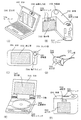
その様な電子機器としては、ビデオカメラ、デジタルカメラ、ヘッドマウントディスプレイ(ゴーグル型ディスプレイ)、カーナビゲーション、プロジェクタ、カーステレオ、パーソナルコンピュータ、携帯情報端末(モバイルコンピュータ、携帯電話または電子書籍等)などが挙げられる。それらの一例を図13〜図15に示す。
【0173】
図13(A)はパーソナルコンピュータであり、本体2001、画像入力部2002、表示部2003、キーボード2004等を含む。本発明を表示部2003に適用することができる。
【0174】
図13(B)はビデオカメラであり、本体2101、表示部2102、音声入力部2103、操作スイッチ2104、バッテリー2105、受像部2106等を含む。本発明を表示部2102に適用することができる。
【0175】
図13(C)はモバイルコンピュータ(モービルコンピュータ)であり、本体2201、カメラ部2202、受像部2203、操作スイッチ2204、表示部2205等を含む。本発明は表示部2205に適用できる。
【0176】
図13(D)はゴーグル型ディスプレイであり、本体2301、表示部2302、アーム部2303等を含む。本発明は表示部2302に適用することができる。
【0177】
図13(E)はプログラムを記録した記録媒体(以下、記録媒体と呼ぶ)を用いるプレーヤーであり、本体2401、表示部2402、スピーカ部2403、記録媒体2404、操作スイッチ2405等を含む。なお、このプレーヤーは記録媒体としてDVD(Digtial Versatile Disc)、CD等を用い、音楽鑑賞や映画鑑賞やゲームやインターネットを行うことができる。本発明は表示部2402に適用することができる。
【0178】
図13(F)はデジタルカメラであり、本体2501、表示部2502、接眼部2503、操作スイッチ2504、受像部(図示しない)等を含む。本発明を表示部2502に適用することができる。
【0179】
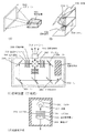
図14(A)はフロント型プロジェクターであり、投射装置2601、スクリーン2602等を含む。本発明は投射装置2601の一部を構成する液晶モジュール2808に適用することができる。
【0180】
図14(B)はリア型プロジェクターであり、本体2701、投射装置2702、ミラー2703、スクリーン2704等を含む。本発明は投射装置2702の一部を構成する液晶モジュール2808に適用することができる。
【0181】
なお、図14(C)は、図14(A)及び図14(B)中における投射装置2601、2702の構造の一例を示した図である。投射装置2601、2702は、光源光学系2801、ミラー2802、2804〜2806、ダイクロイックミラー2803、プリズム2807、液晶モジュール2808、位相差板2809、投射光学系2810で構成される。投射光学系2810は、投射レンズを含む光学系で構成される。本実施例は三板式の例を示したが、特に限定されず、例えば単板式であってもよい。また、図14(C)中において矢印で示した光路に実施者が適宜、光学レンズや、偏光機能を有するフィルムや、位相差を調節するためのフィルム、IRフィルム等の光学系を設けてもよい。
【0182】
また、図14(D)は、図14(C)中における光源光学系2801の構造の一例を示した図である。本実施例では、光源光学系2801は、リフレクター2811、光源2812、レンズアレイ2813、2814、偏光変換素子2815、集光レンズ2816で構成される。なお、図14(D)に示した光源光学系は一例であって特に限定されない。例えば、光源光学系に実施者が適宜、光学レンズや、偏光機能を有するフィルムや、位相差を調節するフィルム、IRフィルム等の光学系を設けてもよい。
【0183】
ただし、図14に示したプロジェクターにおいては、透過型の電気光学装置を用いた場合を示しており、反射型の電気光学装置及びELモジュールでの適用例は図示していない。
【0184】
図15(A)は携帯電話であり、本体2901、音声出力部2902、音声入力部2903、表示部2904、操作スイッチ2905、アンテナ2906、画像入力部(CCD、イメージセンサ等)2907等を含む。本発明を表示部2904に適用することができる。
【0185】
図15(B)は携帯書籍(電子書籍)であり、本体3001、表示部3002、3003、記憶媒体3004、操作スイッチ3005、アンテナ3006等を含む。本発明は表示部3002、3003に適用することができる。
【0186】
図15(C)はディスプレイであり、本体3101、支持台3102、表示部3103等を含む。本発明は表示部3103に適用することができる。
【0187】
以上の様に、本発明の適用範囲は極めて広く、あらゆる分野の電子機器の作製方法に適用することが可能である。また、本実施例の電子機器は実施例1〜7のどのような組み合わせからなる構成を用いても実現することができる。
【0188】
【発明の効果】
本発明により、高温(600℃以上)の加熱処理回数を低減し、さらなる低温プロセス(600℃以下)を実現するとともに、工程簡略化及びスループットの向上を実現することができる。
【0189】
また、希ガス元素を添加する場合、その処理時間は、1分または2分程度の短時間で高濃度の希ガス元素を半導体膜に添加することができるため、リンを用いたゲッタリングと比較してスループットが格段に向上する。
【0190】
また、リンを用いたゲッタリングと比較して、希ガス元素による本発明のゲッタリング能力は高く、さらに高濃度、例えば1×10²⁰〜5×10²¹/cm3で添加できるため、結晶化に用いる金属元素の添加量を多くすることができる。即ち、結晶化に用いる金属元素の添加量を多くすることによって結晶化の処理時間をさらに短時間で行うことが可能となる。また、結晶化の処理時間を変えない場合には、結晶化に用いる金属元素の添加量を多くすることによって、さらなる低温で結晶化することができる。また、結晶化に用いる金属元素の添加量を多くすることによって、自然核の発生を低減することができ、良好な結晶質半導体膜を形成することができる。
【図面の簡単な説明】
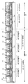
【図1】 TFTの作製工程を示す図。
【図2】 TFTの作製工程を示す図。
【図3】 アクティブマトリクス基板の作製工程を示す図。
【図4】 アクティブマトリクス基板の作製工程を示す図。
【図5】 アクティブマトリクス基板の作製工程を示す図。
【図6】 半導体膜の結晶化を示す図。
【図7】 アクティブマトリクス型液晶表示装置の上面図。
【図8】 透過型の例を示す図。
【図9】 ELモジュールを示す上面図及び断面図。
【図10】 ELモジュールを示す断面図。
【図11】 アクティブマトリクス基板の断面図。
【図12】 アクティブマトリクス基板の断面図及び上面図。
【図13】 電子機器の一例を示す図。
【図14】 電子機器の一例を示す図。
【図15】 電子機器の一例を示す図。
【図16】 アルゴンガス流量と膜の内部応力との関係を示すグラフ。[0001]
BACKGROUND OF THE INVENTION
The present invention relates to a method for manufacturing a semiconductor device using a gettering technique. In particular, the present invention relates to a method for manufacturing a semiconductor device using a crystalline semiconductor film manufactured by adding a metal element having a catalytic action in crystallization of a semiconductor film.
[0002]
Note that in this specification, a semiconductor device refers to all devices that can function by utilizing semiconductor characteristics, and an electro-optical device, a semiconductor circuit, and an electronic device are all semiconductor devices.
[0003]
[Prior art]
As a typical semiconductor element using a semiconductor film having a crystal structure (hereinafter referred to as a crystalline semiconductor film), a thin film transistor (hereinafter referred to as a TFT) is known. TFT is attracting attention as a technique for forming an integrated circuit on an insulating substrate such as glass, and a drive circuit integrated liquid crystal display device or the like is being put into practical use. In a conventional technique, a crystalline semiconductor film is obtained by heating an amorphous semiconductor film deposited by a plasma CVD method or a low pressure CVD method by a heat treatment or a laser annealing method (a technique for crystallizing a semiconductor film by laser light irradiation). Have been made.
[0004]
The crystalline semiconductor film thus manufactured is an aggregate of a large number of crystal grains, and the crystal orientation is oriented in an arbitrary direction and cannot be controlled, which is a factor that limits the characteristics of the TFT. With respect to such problems, the technique disclosed in Japanese Patent Laid-Open No. 7-183540 is a technique for producing a crystalline semiconductor film by adding a metal element having a catalytic action to crystallization of a semiconductor film such as nickel. In addition to the effect of reducing the heating temperature required for crystallization, it is possible to increase the orientation of crystal orientation in a single direction. When a TFT is formed using such a crystalline semiconductor film, not only the field effect mobility is improved, but also the subthreshold coefficient (S value) is reduced, and the electrical characteristics can be dramatically improved. .
[0005]
However, since a metal element having a catalytic action is added, the metal element remains in the film of the crystalline semiconductor film or on the surface of the film, and there is a problem that the characteristics of the obtained element are varied. As an example, there is a problem that an off current increases in a TFT and varies between individual elements. That is, a metal element having a catalytic action for crystallization becomes unnecessary once a crystalline semiconductor film is formed.
[0006]
Gettering using phosphorus is effectively used as a technique for removing such a metal element from a specific region of a crystalline semiconductor film. For example, the metal element can be easily removed from the channel formation region by adding phosphorus to the source / drain region of the TFT and performing heat treatment at 450 to 700 ° C.
[0007]
Phosphorus is a crystalline semiconductor by an ion doping method (a method in which PH 3 is dissociated with plasma and ions are accelerated by an electric field and injected into a semiconductor, and basically does not perform mass separation of ions). Although it is injected into the film, the phosphorus concentration necessary for gettering is 1 × 10 20 / cm 3 or more. Addition of phosphorus by the ion doping method results in the amorphous state of the crystalline semiconductor film, but an increase in the phosphorus concentration poses a problem because it hinders recrystallization by subsequent annealing. Further, the addition of high-concentration phosphorus is problematic because it increases the processing time required for doping and decreases the throughput in the doping process.
[0008]
[Problems to be solved by the invention]
An object of the present invention is to reduce the number of high-temperature (600 ° C. or higher) heat treatments, realize a further low-temperature process (600 ° C. or lower), and simplify the process and improve throughput.
[0009]
[Means for Solving the Problems]
The present invention includes a step of forming a first semiconductor film having a crystal structure using a metal element, a step of forming a film (barrier layer) serving as an etching stopper, a step of forming a second semiconductor film, A step of forming a third semiconductor film (gettering site) containing a rare gas element, a step of gettering a metal element at the gettering site, and a step of removing the second semiconductor film and the third semiconductor film. And have.
[0010]
In addition, in the step of forming the third semiconductor film containing a rare gas element (gettering site), a semiconductor film having an amorphous structure or a crystal structure is formed, and then a rare gas element is added to the semiconductor film. Good. As a method for adding a rare gas element, an ion doping method or an ion implantation method may be used. Note that film formation conditions are adjusted so that film peeling does not occur.
[0011]
In addition to the rare gas element, one or more selected from H, H 2 , O, O 2 , and P may be added. Thus, a gettering effect is synergistically obtained by adding a plurality of elements. Among these, O and O 2 are effective, and the oxygen concentration in the SIMS analysis in the second semiconductor film or the third semiconductor film is 5 × 10 18 / cm 3 or more depending on the film formation conditions or addition after film formation. If the concentration is preferably in the range of 1 × 10 19 / cm 3 to 1 × 10 22 / cm 3 , gettering efficiency is improved. Note that the rare gas element hardly diffuses, but in the case where other elements added in addition to the rare gas element are likely to diffuse, the thickness of the second semiconductor film is adjusted so that the added other elements can be heat-treated later. Thus, it is preferable not to diffuse into the first semiconductor film. In addition to the second semiconductor film, the barrier layer also has a function of preventing diffusion of other elements.
[0012]
In addition, as a step of forming a third semiconductor film (gettering site) containing a rare gas element, a third gas containing a rare gas element is formed by a plasma CVD method using a source gas containing a rare gas element or a low pressure thermal CVD method. The semiconductor film may be formed. However, film forming conditions are adjusted so that film peeling does not occur.
[0013]
Silane gas (SiH 4 : 100 sccm) is used as a deposition gas (flow rate), and an argon gas flow rate is changed to 0 sccm, 100 sccm, 200 sccm, 300 sccm, 400 sccm, and 500 sccm, respectively, and an amorphous silicon film having a thickness of 2000 mm (Sample A) Table 1 shows the experimental results of measuring the internal stress of ~ L).
[0014]
[Table 1]
FIG. 16 shows a graph of Table 1, and an amorphous silicon film by pulse oscillation is shown as a comparative example. When an amorphous silicon film is formed by RF pulse oscillation, the film exhibits compressive stress (about −9.7 × 10 9 (dynes / cm 2 )), so that film peeling may occur. Therefore, it is preferable to form the film by RF continuous oscillation under the conditions having the tensile stress (1.12 to 1.68 × 10 9 (dynes / cm 2 )) shown in Table 1. The second semiconductor film containing no rare gas element may be formed under the conditions of Samples A and B, and the third semiconductor film containing a rare gas element may be formed under any one of the conditions of Samples C to L. preferable.
[0016]
Note that the amorphous silicon film formed by the plasma CVD method (PCVD apparatus) used in the above experiment is formed with an RF power of 35 W and a film forming pressure of 0.25 Torr.
[0017]
Generally, internal stress includes tensile stress and compressive stress. When the thin film is about to shrink with respect to the substrate, the substrate is deformed with the thin film inside because the substrate is pulled in a direction to prevent it, and this is called tensile stress. On the other hand, when the thin film is stretched, the substrate is compressed and formed with the thin film on the outside, and this is called compressive stress.
[0018]
Alternatively, a third semiconductor film containing a rare gas element may be formed by a sputtering method. In this way, after obtaining the third semiconductor film containing a rare gas element in the film formation stage, a rare gas element may be further added to improve the gettering efficiency.
[0019]
The configuration of the first invention disclosed in this specification is as follows.
A first step of adding a metal element to the first semiconductor film having an amorphous structure;
A second step of crystallizing the first semiconductor film to form a first semiconductor film having a crystal structure;
A third step of forming a barrier layer on the surface of the first semiconductor film having the crystal structure;
A fourth step of forming a second semiconductor film on the barrier layer;
A fifth step of forming a third semiconductor film containing a rare gas element at a concentration of 1 × 10 19 to 1 × 10 22 / cm 3 on the second semiconductor film;
A sixth step of removing or reducing the metal element in the first semiconductor film having a crystal structure by gettering the metal element to the third semiconductor film;
And a seventh step of removing the second semiconductor film and the third semiconductor film.
[0020]
In the above structure, the fifth step includes a step of forming a semiconductor film, a step of adding a rare gas element to the semiconductor film, or a third step including a rare gas element by a plasma CVD method or a low pressure thermal CVD method. A step of forming a semiconductor film or a step of forming a third semiconductor film containing a rare gas element by a sputtering method may be used.
[0021]
In the above structure, when a rare gas element is added, one or more selected from O, O 2 , P, H, and H 2 may be added in the same step or sequentially in addition to the rare gas element. preferable.
[0022]
In the above structure, the third semiconductor film is a single layer of a semiconductor film having an amorphous structure or a crystal structure formed by a plasma CVD method, a low pressure thermal CVD method, or a sputtering method, or a stacked layer thereof. It is characterized by that. The third semiconductor film preferably has a tensile stress.
[0023]
The present invention is not limited to the above structure, and a gettering site may be formed by adding a rare gas element only to the upper layer of the second semiconductor film without forming the third semiconductor film.
[0024]
In addition, the configuration of the second invention of the present invention is:
A first step of adding a metal element to the first semiconductor film having an amorphous structure;
A second step of crystallizing the first semiconductor film to form a first semiconductor film having a crystal structure;
A third step of forming a barrier layer on the surface of the first semiconductor film having the crystal structure;
A fourth step of forming a second semiconductor film on the barrier layer;
A fifth step of adding a rare gas element to the upper layer of the second semiconductor film at a concentration of 1 × 10 19 to 1 × 10 22 / cm 3 ;
A sixth step of removing or reducing the metal element in the first semiconductor film having a crystal structure by gettering the metal element on an upper layer of the second semiconductor film;
And a seventh step of removing the second semiconductor film.
[0025]
In the above structure, it is preferable to add one or more selected from O, O 2 , P, H, and H 2 in the same step or sequentially in addition to the rare gas element in the fifth step.
[0026]
In the above two structures, the second semiconductor film is a single layer of a semiconductor film having an amorphous structure or a crystal structure formed by a plasma CVD method, a low pressure thermal CVD method, or a sputtering method, or a stacked layer thereof. It is characterized by being. The second semiconductor film preferably has a tensile stress.
[0027]
In each of the above structures, the metal element is one or more selected from Fe, Ni, Co, Ru, Rh, Pd, Os, Ir, Pt, Cu, and Au.
[0028]
In each of the above configurations, the second step includes heat treatment, irradiation with intense light, or laser light (excimer laser light having a wavelength of 400 nm or less, second harmonic and third harmonic of a YAG laser). One of the irradiation processes is one process, or a combination of these processes.
[0029]
In each of the above structures, the third step of forming the barrier layer includes a step of oxidizing the surface of the semiconductor film having the crystal structure with a solution containing ozone, or the crystal structure by irradiation with ultraviolet rays in an oxygen atmosphere. What is necessary is just to make it the process which is a process of oxidizing the surface of the semiconductor film which has this.
[0030]
In each of the above structures, the sixth step includes a heat treatment, a treatment for irradiating the semiconductor film having an amorphous structure with strong light, or a heat treatment, and the semiconductor having the amorphous structure. The film is characterized by being a process of irradiating the film with intense light.
[0031]
In each of the above structures, when strong light is irradiated, light emitted from a halogen lamp, a metal halide lamp, a xenon arc lamp, a carbon arc lamp, a high-pressure sodium lamp, or a high-pressure mercury lamp may be used.
[0032]
In each of the above structures, the rare gas element is one or a plurality selected from He, Ne, Ar, Kr, and Xe.
[0033]
DETAILED DESCRIPTION OF THE INVENTION
Embodiments of the present invention will be described below.
[0034]
One of the features of the present invention is a process for forming a barrier layer and a semiconductor film on a crystalline semiconductor film, a process for forming a semiconductor film (gettering site) containing a rare gas element above the crystalline semiconductor film, Heat treatment, and the metal contained in the crystalline semiconductor film is moved by the heat treatment and passes through the barrier layer and the semiconductor film (semiconductor film that does not contain ions of the rare gas element). It is captured by (a semiconductor film containing ions of a rare gas element) and a metal element is removed or reduced from the crystalline semiconductor film. Note that strong light may be irradiated instead of the heat treatment, or strong light may be irradiated simultaneously with the heat treatment.
[0035]
(Embodiment 1)
A typical manufacturing procedure will be briefly described below with reference to FIG.
[0036]
In FIG. 1A, 100 is a substrate having an insulating surface, 101 is a base insulating film, and 102 is a semiconductor film having an amorphous structure.
[0037]
First, a
[0038]
Next, the
[0039]
In the present invention, a semiconductor film having a crystal structure is formed by adding a metal element to the
[0040]
After crystallization, a metal element segregated with an etchant containing hydrofluoric acid, for example, dilute hydrofluoric acid or FPM (a mixed solution of hydrofluoric acid, hydrogen peroxide solution, and pure water) may be removed or reduced. In addition, when the surface is etched with an etchant containing hydrofluoric acid, it is desirable to flatten the surface by irradiating with strong light.
[0041]
Further, after the crystallization, laser light or strong light irradiation for further improving the crystallization may be performed. The metal element segregated with an etchant containing hydrofluoric acid may be removed or reduced after irradiation with laser light or strong light to improve crystallization, and the surface may be planarized by further irradiation with strong light. .
[0042]
Note that the oxygen concentration (SIMS analysis) in the
[0043]
Next, a
[0044]
Next, a
[0045]
Next, a third semiconductor film (gettering site) 107 containing a rare gas element is formed over the
[0046]
In the present invention, the
[0047]
Next, gettering is performed. As a step of performing gettering, heat treatment may be performed in a nitrogen atmosphere at 450 to 800 ° C. for 1 to 24 hours, for example, at 550 ° C. for 14 hours. Moreover, you may irradiate strong light instead of heat processing. Moreover, you may irradiate strong light in addition to heat processing. By this gettering, nickel moves in the direction of the arrow in FIG. 1E, and the metal element contained in the
[0048]
Next, after selectively removing only the
[0049]
Next, after cleaning the surface of the semiconductor layer with an etchant containing hydrofluoric acid, an insulating film containing silicon as a main component and serving as the
[0050]
Next, after cleaning the surface of the gate insulating film, a
[0051]
In the subsequent steps, an interlayer insulating film 115 is formed, hydrogenation is performed, contact holes reaching the source region and the drain region are formed, a
[0052]
In the TFT thus obtained, at least the nickel element contained in the
[0053]
In addition, the present invention is not limited to the structure shown in FIG. 1. If necessary, a lightly doped drain (LDD) structure having an LDD region between a channel formation region and a drain region (or source region) may be used. Good. In this structure, a region to which an impurity element is added at a low concentration is provided between a channel formation region and a source region or a drain region formed by adding an impurity element at a high concentration, and this region is referred to as an LDD region. I'm calling. Further, a so-called GOLD (Gate-drain Overlapped LDD) structure in which an LDD region is disposed so as to overlap with a gate electrode through a gate insulating film may be employed.
[0054]
Although an n-channel TFT has been described here, a p-channel TFT can be formed by using an impurity element that imparts p-type to a semiconductor instead of an impurity element that imparts n-type to a semiconductor. Needless to say, you can.
[0055]
Although the top gate TFT has been described as an example here, the present invention can be applied regardless of the TFT structure. Is possible.
[0056]
(Embodiment 2)
Alternatively, the gettering site may be formed by adding a rare gas element only to the upper layer of the second semiconductor film without forming the third semiconductor film shown in Embodiment Mode 1. Here, an example will be described with reference to FIG.
[0057]
The layers up to the
[0058]
Next, a
[0059]
Next, a rare gas element is added to the upper layer of the
[0060]
Next, gettering is performed. As a step of performing gettering, heat treatment may be performed in a nitrogen atmosphere at 450 to 800 ° C. for 1 to 24 hours, for example, at 550 ° C. for 14 hours. Moreover, you may irradiate strong light instead of heat processing. Moreover, you may irradiate strong light in addition to heat processing. By this gettering, nickel moves in the direction of the arrow in FIG. 2E, and the metal element contained in the
[0061]
Next, after selectively removing only the
[0062]
In the subsequent steps, a
[0063]
Also in the TFT obtained in this manner, at least the nickel element contained in the
[0064]
The present invention having the above-described configuration will be described in more detail with the following examples.
[0065]
(Example)
[Example 1]
Here, a method for simultaneously manufacturing a pixel portion and driver circuit TFTs (an n-channel TFT and a p-channel TFT) provided around the pixel portion over the same substrate will be described with reference to FIGS.
[0066]
First, in this embodiment, a
[0067]
Next, a base film 301 made of an insulating film such as a silicon oxide film, a silicon nitride film, or a silicon oxynitride film is formed over the
[0068]
Next, semiconductor layers 302 to 306 are formed over the base film. The semiconductor layers 302 to 306 are formed by forming a semiconductor film having an amorphous structure by a known means (a sputtering method, an LPCVD method, a plasma CVD method, or the like), and then performing a known crystallization process (laser crystallization method, heat A crystalline semiconductor film obtained by performing a crystallization method or a thermal crystallization method using a catalyst such as nickel) is formed by patterning into a desired shape. The semiconductor layers 302 to 306 are formed to a thickness of 25 to 80 nm (preferably 30 to 60 nm). The material of the crystalline semiconductor film is not limited, but is preferably silicon or silicon germanium (Si X Ge 1-X (X = 0.0001 to 0.02)) alloy, for example, germanium content is 0 with respect to silicon. It is preferable to form a silicon germanium film of .02 to 2 atomic%.
[0069]
In this example, a 55 nm amorphous silicon film was formed by plasma CVD, and then a solution containing nickel was held on the amorphous silicon film. This amorphous silicon film is dehydrogenated (500 ° C., 1 hour), then thermally crystallized (550 ° C., 4 hours), and then laser annealing treatment is performed to improve crystallization. Thus, a crystalline silicon film was formed. Then, after forming an extremely thin oxide film on the surface with a solution containing ozone in accordance with Embodiment Mode 1, oxygen (concentration in SIMS analysis is 5 × 10 18 / cm 3 or more, preferably 1 × 10 6 is formed on the oxide film. The second semiconductor film including 19 / cm 3 or more and the third semiconductor film including a rare gas element are formed. Next, after performing gettering in which heat treatment is performed according to Embodiment 1, the second semiconductor film and the third semiconductor film are removed using the oxide film as an etching stopper, and the crystalline silicon film is patterned, and then The oxide film was removed. Thus, semiconductor layers 302 to 306 made of a crystalline silicon film having a nickel concentration of 1 × 10 18 / cm 3 or less, preferably 1 × 10 17 / cm 3 or less were formed. The state in which the patterning of the semiconductor layers 302 to 306 is completed corresponds to FIG. 1F in Embodiment Mode 1. Note that after the oxide film is formed, a small amount of impurity element (boron or phosphorus) may be appropriately doped (also referred to as channel doping) in order to control the threshold value of the TFT.
[0070]
Next, after cleaning the surfaces of the semiconductor layers 302 to 306 with a hydrofluoric acid-based etchant such as buffer hydrofluoric acid, a plasma CVD method or a sputtering method is used to form a thickness of 40 to 150 nm and an insulating
[0071]
Next, as illustrated in FIG. 3A, a first
[0072]
In this embodiment, the first
[0073]
Next, resist
[0074]
Thereafter, the
[0075]
In the first etching process, the shape of the mask made of resist is made suitable, and the end portions of the first conductive layer and the second conductive layer are tapered due to the effect of the bias voltage applied to the substrate side. It becomes. The angle of the tapered portion may be 15 to 45 °.
[0076]
Thus, the first shape conductive layers 316 to 321 (first
[0077]
In this embodiment, following the first etching process, the second etching process is performed without removing the resist mask. Here, SF 6 , Cl 2, and O 2 are used as the etching gas, the gas flow ratios are 24/12/24 (sccm), and a 700 W RF ( 13.56 MHz) Electric power was applied to generate plasma, and etching was performed for 25 seconds. 10 W RF (13.56 MHz) power is also applied to the substrate side (sample stage), and a substantially negative self-bias voltage is applied. In the second etching process, the etching rate with respect to W is 227.3 nm / min, the etching rate with respect to TaN is 32.1 nm / min, the selection ratio of W with respect to TaN is 7.1, and the insulating
[0078]
By this second etching process, the taper angle of W became 70 °. Second
[0079]
Next, after removing the resist mask, a first doping process is performed to obtain the state of FIG. Doping is performed so that the impurity element is not added to the semiconductor layer below the tapered portion of the first conductive layer, using the first
[0080]
In the first doping treatment, doping may be performed so that an impurity element is added to the semiconductor layer below the tapered portion of the first conductive layer. In that case, it has a concentration gradient according to the film thickness of the tapered portion of the first conductive layer.
[0081]
Next, after forming
[0082]
By the second doping treatment, the
[0083]
In addition, high-
[0084]
Further, by the second doping treatment, high-
[0085]
By the second doping treatment, an impurity element imparting n-type is added to the high
[0086]
Further, a rare gas element may be added before and after the second doping treatment, and in that case, gettering can be further performed by a later heat treatment. In that case, it is desirable to use a mask which is added to the end portions of all the semiconductor layers in the second doping process.
[0087]
Next, after removing the
[0088]
In this embodiment, the first doping process, the second doping process, and the third doping process are performed in this order. However, the process order is not particularly limited, and the process order may be freely changed.
[0089]
Next, the resist
[0090]
Next, as shown in FIG. 4C, a step of activating the impurity element added to each semiconductor layer is performed. This activation step is performed by irradiating a YAG laser or excimer laser from the back surface. By irradiating from the back surface, the impurity region overlapping with the gate electrode through the insulating film can be activated.
[0091]
Further, in this embodiment, an example is shown in which the first interlayer insulating film is formed before the activation. However, the first interlayer insulating film may be formed after the activation.
[0092]
Next, a second
[0093]
Next, a third
[0094]
Next,
[0095]
As described above, the driving
[0096]
In this embodiment, the n-
[0097]
The present embodiment is characterized in that high-concentration impurity regions suitable for each circuit are formed separately by the second doping process in a self-aligned manner or by using a mask. The n-
[0098]
Note that in this example, when forming the semiconductor layers 302 to 306, the method for forming a semiconductor layer in Embodiment 2 can be applied instead of the method for forming a semiconductor layer in Embodiment 1.
[0099]
[Example 2]
In this example, an example in which crystallization is performed by a method different from that in Embodiment Mode 1 is shown in FIG.
[0100]
First, a
[0101]
Next, after removing the
[0102]
Next, heat treatment is performed to crystallize, so that a
[0103]
Next, the
[0104]
The subsequent steps may be performed in accordance with Embodiment Mode 1 or Example 1. Note that FIG. 6D corresponds to FIG.
[0105]
In addition, this embodiment can be combined with Embodiment Mode 2.
[0106]
[Example 3]
In this embodiment, a process for manufacturing an active matrix liquid crystal display device from the active matrix substrate manufactured in Embodiment 1 will be described below. FIG. 7 is used for the description.
[0107]
First, after obtaining the active matrix substrate in the state of FIG. 5 according to Example 1, an alignment film is formed on the active matrix substrate of FIG. 5 and a rubbing process is performed. In this embodiment, before the alignment film is formed, columnar spacers for maintaining the distance between the substrates are formed at desired positions by patterning an organic resin film such as an acrylic resin film. Further, instead of the columnar spacers, spherical spacers may be scattered over the entire surface of the substrate.
[0108]
Next, a counter substrate is prepared. The counter substrate is provided with a color filter in which a colored layer and a light shielding layer are arranged corresponding to each pixel. Further, a light shielding layer was also provided in the drive circuit portion. A flattening film covering the color filter and the light shielding layer was provided. Next, a counter electrode made of a transparent conductive film was formed on the planarizing film in the pixel portion, an alignment film was formed on the entire surface of the counter substrate, and a rubbing process was performed.
[0109]
Then, the active matrix substrate on which the pixel portion and the driving circuit are formed and the counter substrate are bonded together with a sealant. A filler is mixed in the sealing material, and two substrates are bonded to each other with a uniform interval by the filler and the columnar spacer. Thereafter, a liquid crystal material is injected between both substrates and completely sealed with a sealant (not shown). A known liquid crystal material may be used as the liquid crystal material. In this way, an active matrix liquid crystal display device is completed. If necessary, the active matrix substrate or the counter substrate is divided into a desired shape. Furthermore, a polarizing plate or the like was appropriately provided using a known technique. And FPC was affixed using the well-known technique.
[0110]
The structure of the liquid crystal module thus obtained will be described with reference to the top view of FIG. In addition, the same code | symbol was used for the part corresponded in FIG.
[0111]
The top view shown in FIG. 7 is a pixel portion, a driving circuit, an
[0112]
A
[0113]
Here, the
[0114]
In addition, a light-shielding layer is provided between adjacent pixels in the color filter to shield light other than the display area. Here, the
[0115]
Further, without providing the light-shielding layer, the light-shielding layer is appropriately disposed between the counter substrate and the counter electrode so as to be shielded from light by stacking a plurality of colored layers constituting the color filter. Or the drive circuit may be shielded from light.
[0116]
An
[0117]
The liquid crystal module manufactured as described above can be used as a display portion of various electronic devices.
[0118]
The liquid crystal module may be AC driven or DC driven.
[0119]
In addition, this embodiment can be freely combined with any one of Embodiment Mode 1, Embodiment Mode 2, Embodiment Mode 1 and Embodiment Mode 2.
[0120]
[Example 4]
In Example 1 or Example 3, an example of a reflective display device in which the pixel electrode is formed of a reflective metal material is shown; however, in this example, the pixel electrode is formed of a light-transmitting conductive film. An example of a transmissive display device is shown.
[0121]
Since the process up to the formation of the
[0122]
Thereafter, contact holes are formed in the
[0123]
Although an example in which all the drive circuits are formed on the substrate is shown here, several ICs may be used as part of the drive circuit.
[0124]
An active matrix substrate is formed as described above. When this active matrix substrate is used to produce a liquid crystal module according to Embodiment 3, and a backlight 1104 and a light guide plate 1105 are provided and covered with a
[0125]
Note that this embodiment can be combined with any one of Embodiments 1 to 3.
[0126]
[Example 5]
In this embodiment, an example of manufacturing a light-emitting display device including an EL (Electro Luminescence) element is shown in FIG.
[0127]
FIG. 9A is a top view showing the EL module, and FIG. 9B is a cross-sectional view taken along line AA ′ of FIG. 9A. A pixel portion 902, a source side driver circuit 901, and a gate side driver circuit 903 are formed over a substrate 900 (eg, a glass substrate, a crystallized glass substrate, or a plastic substrate) having an insulating surface. These pixel portions and driving circuits can be obtained according to the above embodiment.
[0128]
Reference numeral 908 denotes wiring for transmitting signals input to the source side driver circuit 901 and the gate side driver circuit 903, and receives a video signal and a clock signal from an FPC (flexible printed circuit) 909 serving as an external input terminal. Although only the FPC is shown here, a printed wiring board (PWB) may be attached to the FPC. The light-emitting device in this specification includes not only a light-emitting device body but also a state in which an FPC or a PWB is attached thereto.
[0129]
Next, a cross-sectional structure is described with reference to FIG. An insulating film 910 is provided over the substrate 900, and a pixel portion 902 and a gate side driver circuit 903 are formed above the insulating film 910. The pixel portion 902 is electrically connected to the current control TFT 711 and its drain. The
[0130]
These TFTs (including 911, 913, and 914) may be manufactured according to the first embodiment.
[0131]
The
[0132]
As the EL layer 916, an EL layer (a layer for emitting light and moving carriers therefor) may be formed by freely combining a light-emitting layer, a charge transport layer, or a charge injection layer. For example, a low molecular organic EL material or a high molecular organic EL material may be used. As the EL layer, a thin film made of a light emitting material (singlet compound) that emits light (fluorescence) by singlet excitation, or a thin film made of a light emitting material (phosphorescence) that emits light (phosphorescence) by triplet excitation can be used. It is also possible to use an inorganic material such as silicon carbide for the charge transport layer or the charge injection layer. As these organic EL materials and inorganic materials, known materials can be used.
[0133]
The cathode 917 also functions as a wiring common to all pixels, and is electrically connected to the
[0134]
Note that as the
[0135]
In addition, after the light emitting element is completely covered with the
[0136]
By encapsulating the EL element with the sealing
[0137]
Alternatively, the pixel electrode may be a cathode, and an EL layer and an anode may be stacked to emit light in the direction opposite to that in FIG. An example is shown in FIG. Since the top view is the same, it is omitted.
[0138]
The cross-sectional structure shown in FIG. 10 will be described below. As the substrate 1000, a semiconductor substrate or a metal substrate can be used in addition to a glass substrate or a quartz substrate. An insulating film 1010 is provided over the substrate 1000, and a pixel portion 1002 and a gate side driver circuit 1003 are formed above the insulating film 1010. The pixel portion 1002 is electrically connected to the
[0139]
The pixel electrode 1012 functions as a cathode of the EL element. A bank 1015 is formed on both ends of the pixel electrode 1012, and an EL layer 1016 and an EL element anode 1017 are formed on the pixel electrode 1012.
[0140]
The anode 1017 also functions as a wiring common to all pixels, and is electrically connected to the
[0141]
Note that as the
[0142]
In FIG. 10, since the pixel electrode is a cathode and the EL layer and the anode are stacked, the light emission direction is the direction of the arrow shown in FIG.
[0143]
Note that this embodiment can be combined with any one of Embodiments 1 to 4.
[0144]
[Example 6]
In this embodiment, an example different from the first embodiment is shown in FIG.
[0145]
First, a conductive film is formed on the substrate 11 having an insulating surface, and the
[0146]
Next, insulating
[0147]
Next, an amorphous semiconductor film is formed with a thickness of 10 to 100 nm. Here, an amorphous silicon film (amorphous silicon film) having a thickness of 69 nm is formed by LPCVD. Next, as a technique for crystallizing this amorphous semiconductor film, crystallization, gettering, and patterning are performed using the technique shown in Embodiment 1 or Embodiment 2 to remove unnecessary portions of the crystalline silicon film. Thus, the
[0148]
Next, in order to form a storage capacitor, a mask is formed, and a part of the semiconductor layer (a region to be a storage capacitor) is doped with phosphorus.
[0149]
Next, after removing the mask and forming an insulating film that covers the semiconductor layer, the insulating film on the region that forms the storage capacitor by forming the mask is selectively removed.
[0150]
Next, the mask is removed, and thermal oxidation is performed to form an insulating film (gate insulating film) 15. By this thermal oxidation, the final gate insulating film thickness was 80 nm. Note that an insulating film thinner than other regions was formed over the region serving as the storage capacitor.
[0151]
Next, a channel doping process for adding a p-type or n-type impurity element at a low concentration to a region to be a channel region of the TFT was performed over the entire surface or selectively. This channel doping process is a process for controlling the TFT threshold voltage. Here, boron was added by an ion doping method in which diborane (B 2 H 6 ) was plasma-excited without mass separation. Of course, an ion implantation method that performs mass separation may be used.
[0152]
Next, a mask is formed over the insulating
[0153]
Next, a conductive film is formed and patterned to form the
[0154]
Next, phosphorus is added at a low concentration in a self-aligning manner using the
[0155]
Next, a mask is formed, phosphorus is added at a high concentration, and a high concentration impurity region which becomes a source region or a drain region is formed. The concentration of phosphorus in this high concentration impurity region is adjusted to 1 × 10 20 to 1 × 10 21 atoms / cm 3 (typically 3 × 10 19 to 3 × 10 20 / cm 3 ). Note that in the
[0156]
Next, in order to form a p-channel TFT used for a driver circuit formed over the same substrate as the pixel, a region to be an n-channel TFT is covered with a mask, and boron is added to form a source region or a drain region. .
[0157]
Next, after removing the mask 412, a
[0158]
Next, an
[0159]
Next, after performing a hydrogenation process, an
[0160]
Needless to say, the present embodiment is an example and is not limited to the steps of the present embodiment. For example, as each conductive film, an element selected from tantalum (Ta), titanium (Ti), molybdenum (Mo), tungsten (W), chromium (Cr), silicon (Si), or an alloy in which the elements are combined A film (typically, a Mo—W alloy or a Mo—Ta alloy) can be used. As each insulating film, a silicon oxide film, a silicon nitride film, a silicon oxynitride film, or an organic resin material (polyimide, acrylic, polyamide, polyimide amide, BCB (benzocyclobutene), or the like) film can be used.
[0161]
Note that this embodiment can be combined with any one of Embodiments 1 to 5.
[0162]
[Example 7]
In Embodiment 1, the top gate TFT has been described as an example, but the present invention can also be applied to the bottom gate TFT shown in FIG.
[0163]
12A is an enlarged top view of one of the pixels in the pixel portion. In FIG. 12A, a portion cut along a dotted line AA ′ is a cross section of the pixel portion in FIG. Corresponds to the structure.
[0164]
In the pixel portion shown in FIG. 12, the pixel TFT portion is formed of an N-channel TFT. A
[0165]
In this example, the active layer is formed according to the first embodiment or the second embodiment described above.
[0166]
In this embodiment, an example of a channel stop type bottom gate type TFT is shown as an example, but it is not particularly limited.
[0167]
In this embodiment, the gate wiring of the pixel TFT in the pixel portion has a double gate structure. However, a multi-gate structure such as a triple gate structure may be used in order to reduce variation in off current. Further, a single gate structure may be used in order to improve the aperture ratio.
[0168]
Further, the capacitor portion of the pixel portion is formed by the
[0169]
Note that the pixel portion illustrated in FIG. 12 is merely an example, and needless to say, the configuration is not particularly limited to the above configuration.
[0170]
Note that this embodiment can be combined with any one of Embodiments 1 to 4.
[0171]
[Example 8]
The driver circuit and the pixel portion formed by implementing the present invention can be used for various modules (active matrix liquid crystal module, active matrix EL module, active matrix EC module). That is, the present invention can be implemented in all electronic devices in which they are incorporated in the display portion.
[0172]
Such electronic devices include video cameras, digital cameras, head mounted displays (goggles type displays), car navigation systems, projectors, car stereos, personal computers, personal digital assistants (mobile computers, mobile phones, electronic books, etc.), etc. Can be mentioned. Examples of these are shown in FIGS.
[0173]
FIG. 13A illustrates a personal computer, which includes a main body 2001, an image input portion 2002, a display portion 2003, a
[0174]
FIG. 13B illustrates a video camera, which includes a main body 2101, a display portion 2102, an
[0175]
FIG. 13C illustrates a mobile computer, which includes a main body 2201, a camera unit 2202, an
[0176]
FIG. 13D shows a goggle type display, which includes a
[0177]
FIG. 13E shows a player using a recording medium (hereinafter referred to as a recording medium) on which a program is recorded, and includes a main body 2401, a
[0178]
FIG. 13F illustrates a digital camera, which includes a main body 2501, a
[0179]
FIG. 14A illustrates a front type projector, which includes a
[0180]
FIG. 14B shows a rear projector, which includes a main body 2701, a
[0181]
FIG. 14C is a diagram showing an example of the structure of the
[0182]
FIG. 14D shows an example of the structure of the light source
[0183]
However, the projector shown in FIG. 14 shows a case where a transmissive electro-optical device is used, and an application example in a reflective electro-optical device and an EL module is not shown.
[0184]
FIG. 15A shows a cellular phone, which includes a
[0185]
FIG. 15B illustrates a portable book (electronic book), which includes a
[0186]
FIG. 15C illustrates a display, which includes a
[0187]
As described above, the applicable range of the present invention is so wide that the present invention can be applied to methods for manufacturing electronic devices in various fields. Moreover, the electronic apparatus of a present Example is realizable even if it uses the structure which consists of what combination of Examples 1-7.
[0188]
【Effect of the invention】
According to the present invention, the number of high-temperature (600 ° C. or higher) heat treatments can be reduced, a further low-temperature process (600 ° C. or lower) can be realized, and the process can be simplified and the throughput can be improved.
[0189]
In addition, when a rare gas element is added, a high concentration of the rare gas element can be added to the semiconductor film in a short time of about 1 minute or 2 minutes, which is compared with gettering using phosphorus. As a result, the throughput is remarkably improved.
[0190]
Further, compared with gettering using phosphorus, the gettering ability of the present invention by a rare gas element is high, and can be added at a high concentration, for example, 1 × 10 20 to 5 × 10 21 / cm 3 . It is possible to increase the amount of the metal element used for. In other words, the crystallization treatment time can be further shortened by increasing the amount of the metal element used for crystallization. In the case where the treatment time for crystallization is not changed, crystallization can be performed at a further lower temperature by increasing the amount of the metal element used for crystallization. Further, by increasing the amount of the metal element used for crystallization, the generation of natural nuclei can be reduced and a good crystalline semiconductor film can be formed.
[Brief description of the drawings]
FIGS. 1A and 1B illustrate a manufacturing process of a TFT. FIGS.
FIGS. 2A and 2B are diagrams illustrating a manufacturing process of a TFT. FIGS.
FIGS. 3A and 3B are diagrams illustrating a manufacturing process of an active matrix substrate. FIGS.
FIGS. 4A and 4B are diagrams illustrating a manufacturing process of an active matrix substrate. FIGS.
FIGS. 5A and 5B are diagrams illustrating a manufacturing process of an active matrix substrate. FIGS.
FIG. 6 shows crystallization of a semiconductor film.
FIG. 7 is a top view of an active matrix liquid crystal display device.
FIG. 8 is a diagram showing an example of a transmission type.
FIGS. 9A and 9B are a top view and a cross-sectional view illustrating an EL module. FIGS.
FIG. 10 is a cross-sectional view showing an EL module.
FIG. 11 is a cross-sectional view of an active matrix substrate.
12A and 12B are a cross-sectional view and a top view of an active matrix substrate.
FIG 13 illustrates an example of an electronic device.
FIG 14 illustrates an example of an electronic device.
FIG 15 illustrates an example of an electronic device.
FIG. 16 is a graph showing the relationship between the argon gas flow rate and the internal stress of the film.
Claims (13)
前記非晶質構造を有する第1の半導体膜を結晶化させて結晶構造を有する第1の半導体膜を形成し、
前記結晶構造を有する第1の半導体膜の表面にバリア層を形成し、
前記バリア層上に第2の半導体膜を形成し、
前記第2の半導体膜上に希ガス元素を含む第3の半導体膜を形成し、
前記第3の半導体膜に前記金属元素をゲッタリングして、前記結晶構造を有する第1の半導体膜中の前記金属元素を低減し、
前記バリア層をエッチングストッパーとして用いて、前記第2の半導体膜及び前記第3の半導体膜を除去することを特徴とする半導体装置の作製方法。A metal element having a catalytic action for crystallization of the first semiconductor film having an amorphous structure is added to the first semiconductor film having the amorphous structure ;
Crystallizing the first semiconductor film having an amorphous structure to form a first semiconductor film having a crystalline structure;
Forming a barrier layer on the surface of the first semiconductor film having the crystal structure;
Forming a second semiconductor film on the barrier layer;
Forming a third semiconductor film containing a rare gas element on the second semiconductor film;
Gettering the metal element to the third semiconductor film to reduce the metal element in the first semiconductor film having the crystal structure;
A method for manufacturing a semiconductor device, wherein the second semiconductor film and the third semiconductor film are removed using the barrier layer as an etching stopper.
前記第3の半導体膜に、前記希ガス元素を1×10¹⁹〜1×10²²/cm3の濃度で添加することを特徴とする半導体装置の作製方法。In claim 1 ,
A method for manufacturing a semiconductor device, wherein the rare gas element is added to the third semiconductor film at a concentration of 1 × 10 19 to 1 × 10 22 / cm 3 .
前記非晶質構造を有する第1の半導体膜を結晶化させて結晶構造を有する第1の半導体膜を形成し、
前記結晶構造を有する第1の半導体膜の表面にバリア層を形成し、
前記バリア層上に第2の半導体膜を形成し、
前記第2の半導体膜上に第3の半導体膜を形成し、
前記第3の半導体膜に希ガス元素を添加し、
前記第3の半導体膜に前記金属元素をゲッタリングして、前記結晶構造を有する第1の半導体膜中の前記金属元素を低減し、
前記バリア層をエッチングストッパーとして用いて、前記第2の半導体膜及び前記第3の半導体膜を除去することを特徴とする半導体装置の作製方法。A metal element having a catalytic action for crystallization of the first semiconductor film having an amorphous structure is added to the first semiconductor film having the amorphous structure ;
Crystallizing the first semiconductor film having an amorphous structure to form a first semiconductor film having a crystalline structure;
Forming a barrier layer on the surface of the first semiconductor film having the crystal structure;
Forming a second semiconductor film on the barrier layer;
Forming a third semiconductor film on the second semiconductor film;
Adding a rare gas element to the third semiconductor film;
Gettering the metal element to the third semiconductor film to reduce the metal element in the first semiconductor film having the crystal structure;
A method for manufacturing a semiconductor device, wherein the second semiconductor film and the third semiconductor film are removed using the barrier layer as an etching stopper.
前記第3の半導体膜に、さらにO、O2、P、H、H2から選ばれた一種または複数種を添加することを特徴とする半導体装置の作製方法。In any one of Claims 1 thru | or 3 ,
A method for manufacturing a semiconductor device, wherein one or more selected from O, O 2 , P, H, and H 2 are further added to the third semiconductor film.
前記非晶質構造を有する第1の半導体膜を結晶化させて結晶構造を有する第1の半導体膜を形成し、
前記結晶構造を有する第1の半導体膜の表面にバリア層を形成し、
前記バリア層上に第2の半導体膜を形成し、
前記第2の半導体膜の上層に希ガス元素を添加し、
前記第2の半導体膜の上層に前記金属元素をゲッタリングして、前記結晶構造を有する第1の半導体膜中の前記金属元素を低減し、
前記バリア層をエッチングストッパーとして用いて、前記第2の半導体膜を除去することを特徴とする半導体装置の作製方法。A metal element having a catalytic action for crystallization of the first semiconductor film having an amorphous structure is added to the first semiconductor film having the amorphous structure ;
Crystallizing the first semiconductor film having an amorphous structure to form a first semiconductor film having a crystalline structure;
Forming a barrier layer on the surface of the first semiconductor film having the crystal structure;
Forming a second semiconductor film on the barrier layer;
Adding a rare gas element to the upper layer of the second semiconductor film;
Gettering the metal element on an upper layer of the second semiconductor film to reduce the metal element in the first semiconductor film having the crystal structure;
A method for manufacturing a semiconductor device, wherein the second semiconductor film is removed using the barrier layer as an etching stopper.
前記第2の半導体膜の上層に、前記希ガス元素を1×10¹⁹〜1×10²²/cm3の濃度で添加することを特徴とする半導体装置の作製方法。In claim 5 ,
A method for manufacturing a semiconductor device, wherein the rare gas element is added to the upper layer of the second semiconductor film at a concentration of 1 × 10 19 to 1 × 10 22 / cm 3 .
前記第2の半導体膜の上層に、さらにO、O2、P、H、H2から選ばれた一種または複数種を添加することを特徴とする半導体装置の作製方法。In claim 5 or claim 6 ,
A method for manufacturing a semiconductor device, wherein one or more selected from O, O 2 , P, H, and H 2 are further added to the upper layer of the second semiconductor film.
加熱処理、強光を照射する処理、またはレーザー光を照射する処理の内、いずれか一の処理、もしくはこれらを組み合わせた処理によって、前記非晶質構造を有する第1の半導体膜を結晶化させることを特徴とする半導体装置の作製方法。In any one of Claims 1 thru | or 7 ,
The first semiconductor film having the amorphous structure is crystallized by any one of heat treatment, intense light irradiation, or laser light irradiation treatment or a combination thereof. A method for manufacturing a semiconductor device.
加熱処理または強光を照射する処理によって、前記金属元素をゲッタリングすることを特徴とする半導体装置の作製方法。In any one of Claims 1 thru | or 8 ,
A method for manufacturing a semiconductor device, characterized in that the metal element is gettered by heat treatment or strong light irradiation treatment.
前記金属元素は、Fe、Ni、Co、Ru、Rh、Pd、Os、Ir、Pt、Cu、Auから選ばれた一種または複数種であることを特徴とする半導体装置の作製方法。In any one of Claims 1 thru | or 9 ,
The method for manufacturing a semiconductor device, wherein the metal element is one or more selected from Fe, Ni, Co, Ru, Rh, Pd, Os, Ir, Pt, Cu, and Au.
前記バリア層を、オゾンを含む溶液で前記結晶構造を有する第1の半導体膜の表面を酸化することによって形成することを特徴とする半導体装置の作製方法。In any one of Claims 1 to 10 ,
The method for manufacturing a semiconductor device, wherein the barrier layer is formed by oxidizing a surface of the first semiconductor film having the crystal structure with a solution containing ozone.
前記バリア層を、紫外線の照射で前記結晶構造を有する第1の半導体膜の表面を酸化することによって形成することを特徴とする半導体装置の作製方法。In any one of Claims 1 to 10 ,
The method for manufacturing a semiconductor device, wherein the barrier layer is formed by oxidizing the surface of the first semiconductor film having the crystal structure by irradiation with ultraviolet rays.
前記希ガス元素は、He、Ne、Ar、Kr、Xeから選ばれた一種または複数種であることを特徴とする半導体装置の作製方法。In any one of Claims 1 to 12 ,
The method of manufacturing a semiconductor device, wherein the rare gas element is one or more selected from He, Ne, Ar, Kr, and Xe.
Priority Applications (3)
| Application Number | Priority Date | Filing Date | Title |
|---|---|---|---|
| JP2001040837A JP4993810B2 (en) | 2001-02-16 | 2001-02-16 | Method for manufacturing semiconductor device |
| US10/072,931 US7316947B2 (en) | 2001-02-16 | 2002-02-12 | Method of manufacturing a semiconductor device |
| US11/882,907 US7538011B2 (en) | 2001-02-16 | 2007-08-07 | Method of manufacturing a semiconductor device |
Applications Claiming Priority (1)
| Application Number | Priority Date | Filing Date | Title |
|---|---|---|---|
| JP2001040837A JP4993810B2 (en) | 2001-02-16 | 2001-02-16 | Method for manufacturing semiconductor device |
Publications (3)
| Publication Number | Publication Date |
|---|---|
| JP2002246394A JP2002246394A (en) | 2002-08-30 |
| JP2002246394A5 JP2002246394A5 (en) | 2008-03-13 |
| JP4993810B2 true JP4993810B2 (en) | 2012-08-08 |
Family
ID=18903361
Family Applications (1)
| Application Number | Title | Priority Date | Filing Date |
|---|---|---|---|
| JP2001040837A Expired - Fee Related JP4993810B2 (en) | 2001-02-16 | 2001-02-16 | Method for manufacturing semiconductor device |
Country Status (2)
| Country | Link |
|---|---|
| US (2) | US7316947B2 (en) |
| JP (1) | JP4993810B2 (en) |
Families Citing this family (25)
| Publication number | Priority date | Publication date | Assignee | Title |
|---|---|---|---|---|
| JP4056571B2 (en) | 1995-08-02 | 2008-03-05 | 株式会社半導体エネルギー研究所 | Method for manufacturing semiconductor device |
| US7503975B2 (en) * | 2000-06-27 | 2009-03-17 | Semiconductor Energy Laboratory Co., Ltd. | Semiconductor device and fabrication method therefor |
| US7045444B2 (en) | 2000-12-19 | 2006-05-16 | Semiconductor Energy Laboratory Co., Ltd. | Method of manufacturing semiconductor device that includes selectively adding a noble gas element |
| US6858480B2 (en) * | 2001-01-18 | 2005-02-22 | Semiconductor Energy Laboratory Co., Ltd. | Method of manufacturing semiconductor device |
| JP2002231627A (en) | 2001-01-30 | 2002-08-16 | Semiconductor Energy Lab Co Ltd | Method of manufacturing photoelectric conversion unit |
| US7141822B2 (en) * | 2001-02-09 | 2006-11-28 | Semiconductor Energy Laboratory Co., Ltd. | Semiconductor device and method for manufacturing the same |
| JP4993810B2 (en) * | 2001-02-16 | 2012-08-08 | 株式会社半導体エネルギー研究所 | Method for manufacturing semiconductor device |
| US7052943B2 (en) * | 2001-03-16 | 2006-05-30 | Semiconductor Energy Laboratory Co., Ltd. | Method of manufacturing a semiconductor device |
| JP4718700B2 (en) * | 2001-03-16 | 2011-07-06 | 株式会社半導体エネルギー研究所 | Method for manufacturing semiconductor device |
| TW541584B (en) * | 2001-06-01 | 2003-07-11 | Semiconductor Energy Lab | Semiconductor film, semiconductor device and method for manufacturing same |
| US6743700B2 (en) * | 2001-06-01 | 2004-06-01 | Semiconductor Energy Laboratory Co., Ltd. | Semiconductor film, semiconductor device and method of their production |
| US7199027B2 (en) * | 2001-07-10 | 2007-04-03 | Semiconductor Energy Laboratory Co., Ltd. | Method of manufacturing a semiconductor film by plasma CVD using a noble gas and nitrogen |
| JP5072157B2 (en) * | 2001-09-27 | 2012-11-14 | 株式会社半導体エネルギー研究所 | Method for manufacturing semiconductor device |
| US7091110B2 (en) * | 2002-06-12 | 2006-08-15 | Semiconductor Energy Laboratory Co., Ltd. | Method of manufacturing a semiconductor device by gettering using a anti-diffusion layer |
| US7332431B2 (en) * | 2002-10-17 | 2008-02-19 | Semiconductor Energy Laboratory Co., Ltd. | Method of manufacturing semiconductor device |
| US6815077B1 (en) * | 2003-05-20 | 2004-11-09 | Matrix Semiconductor, Inc. | Low temperature, low-resistivity heavily doped p-type polysilicon deposition |
| US7459379B2 (en) * | 2004-03-26 | 2008-12-02 | Semiconductor Energy Laboratory Co., Ltd. | Method for manufacturing semiconductor device |
| US7402465B2 (en) * | 2004-11-11 | 2008-07-22 | Samsung Electronics Co., Ltd. | Method of fabricating single-crystal silicon film and method of fabricating TFT adopting the same |
| US8003449B2 (en) | 2004-11-26 | 2011-08-23 | Semiconductor Energy Laboratory Co., Ltd. | Method of manufacturing a semiconductor device having a reverse staggered thin film transistor |
| US7791172B2 (en) * | 2007-03-19 | 2010-09-07 | Semiconductor Energy Laboratory Co., Ltd. | Nonvolatile semiconductor memory device |
| CN101681843B (en) * | 2007-06-20 | 2012-05-09 | 株式会社半导体能源研究所 | Method of manufacturing semiconductor device |
| US7795111B2 (en) * | 2007-06-27 | 2010-09-14 | Semiconductor Energy Laboratory Co., Ltd. | Manufacturing method of SOI substrate and manufacturing method of semiconductor device |
| CN104733540B (en) | 2009-10-09 | 2019-11-12 | 株式会社半导体能源研究所 | Semiconductor devices |
| US8395156B2 (en) * | 2009-11-24 | 2013-03-12 | Semiconductor Energy Laboratory Co., Ltd. | Display device |
| US8647439B2 (en) | 2012-04-26 | 2014-02-11 | Applied Materials, Inc. | Method of epitaxial germanium tin alloy surface preparation |
Family Cites Families (150)
| Publication number | Priority date | Publication date | Assignee | Title |
|---|---|---|---|---|
| US3535775A (en) * | 1967-12-18 | 1970-10-27 | Gen Electric | Formation of small semiconductor structures |
| JPS5693367A (en) * | 1979-12-20 | 1981-07-28 | Fujitsu Ltd | Manufacture of semiconductor device |
| US4534820A (en) * | 1981-10-19 | 1985-08-13 | Nippon Telegraph & Telephone Public Corporation | Method for manufacturing crystalline film |
| US4477308A (en) * | 1982-09-30 | 1984-10-16 | At&T Bell Laboratories | Heteroepitaxy of multiconstituent material by means of a _template layer |
| US4608096A (en) * | 1983-04-04 | 1986-08-26 | Monsanto Company | Gettering |
| US4727044A (en) | 1984-05-18 | 1988-02-23 | Semiconductor Energy Laboratory Co., Ltd. | Method of making a thin film transistor with laser recrystallized source and drain |
| US5248630A (en) | 1987-07-27 | 1993-09-28 | Nippon Telegraph And Telephone Corporation | Thin film silicon semiconductor device and process for producing thereof |
| TW237562B (en) * | 1990-11-09 | 1995-01-01 | Semiconductor Energy Res Co Ltd | |
| SG47403A1 (en) * | 1990-12-05 | 1998-04-17 | At & T Corp | Lithographic techniques |
| JPH0824104B2 (en) | 1991-03-18 | 1996-03-06 | 株式会社半導体エネルギー研究所 | Semiconductor material and manufacturing method thereof |
| US5244819A (en) * | 1991-10-22 | 1993-09-14 | Honeywell Inc. | Method to getter contamination in semiconductor devices |
| US5229305A (en) * | 1992-02-03 | 1993-07-20 | Motorola, Inc. | Method for making intrinsic gettering sites in bonded substrates |
| CN1244891C (en) | 1992-08-27 | 2006-03-08 | 株式会社半导体能源研究所 | Active matrix display |
| TW226478B (en) * | 1992-12-04 | 1994-07-11 | Semiconductor Energy Res Co Ltd | Semiconductor device and method for manufacturing the same |
| US5604360A (en) * | 1992-12-04 | 1997-02-18 | Semiconductor Energy Laboratory Co., Ltd. | Semiconductor device including a plurality of thin film transistors at least some of which have a crystalline silicon film crystal-grown substantially in parallel to the surface of a substrate for the transistor |
| US6022458A (en) * | 1992-12-07 | 2000-02-08 | Canon Kabushiki Kaisha | Method of production of a semiconductor substrate |
| US5843225A (en) * | 1993-02-03 | 1998-12-01 | Semiconductor Energy Laboratory Co., Ltd. | Process for fabricating semiconductor and process for fabricating semiconductor device |
| JPH06296023A (en) * | 1993-02-10 | 1994-10-21 | Semiconductor Energy Lab Co Ltd | Thin-film semiconductor device and manufacture thereof |
| EP0612102B1 (en) | 1993-02-15 | 2001-09-26 | Semiconductor Energy Laboratory Co., Ltd. | Process for the fabrication of a crystallised semiconductor layer |
| JP3662263B2 (en) | 1993-02-15 | 2005-06-22 | 株式会社半導体エネルギー研究所 | Method for manufacturing semiconductor device |
| JP3107941B2 (en) | 1993-03-05 | 2000-11-13 | 株式会社半導体エネルギー研究所 | Thin film transistor and manufacturing method thereof |
| TW278219B (en) * | 1993-03-12 | 1996-06-11 | Handotai Energy Kenkyusho Kk | |
| JP3193803B2 (en) * | 1993-03-12 | 2001-07-30 | 株式会社半導体エネルギー研究所 | Manufacturing method of semiconductor element |
| US5624851A (en) * | 1993-03-12 | 1997-04-29 | Semiconductor Energy Laboratory Co., Ltd. | Process of fabricating a semiconductor device in which one portion of an amorphous silicon film is thermally crystallized and another portion is laser crystallized |
| TW241377B (en) * | 1993-03-12 | 1995-02-21 | Semiconductor Energy Res Co Ltd | |
| KR100203982B1 (en) * | 1993-03-12 | 1999-06-15 | 야마자끼 순페이 | Semiconductor device and manufacturing method thereof |
| US5501989A (en) * | 1993-03-22 | 1996-03-26 | Semiconductor Energy Laboratory Co., Ltd. | Method of making semiconductor device/circuit having at least partially crystallized semiconductor layer |
| US5481121A (en) * | 1993-05-26 | 1996-01-02 | Semiconductor Energy Laboratory Co., Ltd. | Semiconductor device having improved crystal orientation |
| JP3253759B2 (en) * | 1993-06-08 | 2002-02-04 | 株式会社東芝 | Semiconductor device and manufacturing method thereof |
| JPH06349735A (en) * | 1993-06-12 | 1994-12-22 | Semiconductor Energy Lab Co Ltd | Semiconductor device |
| US5488000A (en) * | 1993-06-22 | 1996-01-30 | Semiconductor Energy Laboratory Co., Ltd. | Method of fabricating a thin film transistor using a nickel silicide layer to promote crystallization of the amorphous silicon layer |
| US5529937A (en) | 1993-07-27 | 1996-06-25 | Semiconductor Energy Laboratory Co., Ltd. | Process for fabricating thin film transistor |
| US5663077A (en) * | 1993-07-27 | 1997-09-02 | Semiconductor Energy Laboratory Co., Ltd. | Method of manufacturing a thin film transistor in which the gate insulator comprises two oxide films |
| US5492843A (en) * | 1993-07-31 | 1996-02-20 | Semiconductor Energy Laboratory Co., Ltd. | Method of fabricating semiconductor device and method of processing substrate |
| JP2975973B2 (en) * | 1993-08-10 | 1999-11-10 | 株式会社半導体エネルギー研究所 | Semiconductor device and manufacturing method thereof |
| JP2762215B2 (en) * | 1993-08-12 | 1998-06-04 | 株式会社半導体エネルギー研究所 | Method for manufacturing thin film transistor and semiconductor device |
| JP2814049B2 (en) * | 1993-08-27 | 1998-10-22 | 株式会社半導体エネルギー研究所 | Semiconductor device and manufacturing method thereof |
| US5923962A (en) * | 1993-10-29 | 1999-07-13 | Semiconductor Energy Laboratory Co., Ltd. | Method for manufacturing a semiconductor device |
| TW264575B (en) * | 1993-10-29 | 1995-12-01 | Handotai Energy Kenkyusho Kk | |
| US5612250A (en) * | 1993-12-01 | 1997-03-18 | Semiconductor Energy Laboratory Co., Ltd. | Method for manufacturing a semiconductor device using a catalyst |
| JP3562590B2 (en) * | 1993-12-01 | 2004-09-08 | 株式会社半導体エネルギー研究所 | Semiconductor device manufacturing method |
| US5654203A (en) * | 1993-12-02 | 1997-08-05 | Semiconductor Energy Laboratory, Co., Ltd. | Method for manufacturing a thin film transistor using catalyst elements to promote crystallization |
| JP2860869B2 (en) * | 1993-12-02 | 1999-02-24 | 株式会社半導体エネルギー研究所 | Semiconductor device and manufacturing method thereof |
| TW273574B (en) | 1993-12-10 | 1996-04-01 | Tokyo Electron Co Ltd | |
| TW272319B (en) | 1993-12-20 | 1996-03-11 | Sharp Kk | |
| KR100319332B1 (en) * | 1993-12-22 | 2002-04-22 | 야마자끼 순페이 | Semiconductor device and electro-optical device |
| TW279275B (en) | 1993-12-27 | 1996-06-21 | Sharp Kk | |
| JP3378078B2 (en) * | 1994-02-23 | 2003-02-17 | 株式会社半導体エネルギー研究所 | Method for manufacturing semiconductor device |
| JP3352340B2 (en) * | 1995-10-06 | 2002-12-03 | キヤノン株式会社 | Semiconductor substrate and method of manufacturing the same |
| US6162667A (en) * | 1994-03-28 | 2000-12-19 | Sharp Kabushiki Kaisha | Method for fabricating thin film transistors |
| JPH07335906A (en) * | 1994-06-14 | 1995-12-22 | Semiconductor Energy Lab Co Ltd | Thin film semiconductor device and fabrication thereof |
| JP3190520B2 (en) | 1994-06-14 | 2001-07-23 | 株式会社半導体エネルギー研究所 | Semiconductor device and manufacturing method thereof |
| JP3067949B2 (en) * | 1994-06-15 | 2000-07-24 | シャープ株式会社 | Electronic device and liquid crystal display device |
| JP3504336B2 (en) | 1994-06-15 | 2004-03-08 | 株式会社半導体エネルギー研究所 | Method for manufacturing semiconductor device |
| JP3072000B2 (en) * | 1994-06-23 | 2000-07-31 | 株式会社半導体エネルギー研究所 | Method for manufacturing semiconductor device |
| JP3076202B2 (en) * | 1994-07-12 | 2000-08-14 | 三菱マテリアルシリコン株式会社 | Method of depositing polysilicon film for EG |
| TW280943B (en) | 1994-07-15 | 1996-07-11 | Sharp Kk | |
| EP0694960B1 (en) * | 1994-07-25 | 2002-07-03 | Consorzio per la Ricerca sulla Microelettronica nel Mezzogiorno - CoRiMMe | Process for the localized reduction of the lifetime of charge carriers |
| US5712191A (en) * | 1994-09-16 | 1998-01-27 | Semiconductor Energy Laboratory Co., Ltd. | Method for producing semiconductor device |
| US5789284A (en) * | 1994-09-29 | 1998-08-04 | Semiconductor Energy Laboratory Co., Ltd. | Method for fabricating semiconductor thin film |
| US5915174A (en) | 1994-09-30 | 1999-06-22 | Semiconductor Energy Laboratory Co., Ltd. | Semiconductor device and method for producing the same |
| JP3942651B2 (en) * | 1994-10-07 | 2007-07-11 | 株式会社半導体エネルギー研究所 | Method for manufacturing semiconductor device |
| JP3486240B2 (en) * | 1994-10-20 | 2004-01-13 | 株式会社半導体エネルギー研究所 | Semiconductor device |
| JP3138169B2 (en) | 1995-03-13 | 2001-02-26 | シャープ株式会社 | Method for manufacturing semiconductor device |
| TW447144B (en) | 1995-03-27 | 2001-07-21 | Semiconductor Energy Lab | Semiconductor device and a method of manufacturing the same |
| FR2738671B1 (en) * | 1995-09-13 | 1997-10-10 | Commissariat Energie Atomique | PROCESS FOR PRODUCING THIN FILMS WITH SEMICONDUCTOR MATERIAL |
| US5977559A (en) | 1995-09-29 | 1999-11-02 | Semiconductor Energy Laboratory Co., Ltd. | Thin-film transistor having a catalyst element in its active regions |
| US6391690B2 (en) * | 1995-12-14 | 2002-05-21 | Seiko Epson Corporation | Thin film semiconductor device and method for producing the same |
| US6204101B1 (en) | 1995-12-15 | 2001-03-20 | Semiconductor Energy Laboratory Co., Ltd. | Method of manufacturing semiconductor device |
| TW319912B (en) | 1995-12-15 | 1997-11-11 | Handotai Energy Kenkyusho Kk | |
| JP3645379B2 (en) | 1996-01-19 | 2005-05-11 | 株式会社半導体エネルギー研究所 | Method for manufacturing semiconductor device |
| JP3729955B2 (en) | 1996-01-19 | 2005-12-21 | 株式会社半導体エネルギー研究所 | Method for manufacturing semiconductor device |
| US5985740A (en) | 1996-01-19 | 1999-11-16 | Semiconductor Energy Laboratory Co., Ltd. | Method of manufacturing a semiconductor device including reduction of a catalyst |
| US5888858A (en) | 1996-01-20 | 1999-03-30 | Semiconductor Energy Laboratory Co., Ltd. | Semiconductor device and fabrication method thereof |
| JP3910229B2 (en) * | 1996-01-26 | 2007-04-25 | 株式会社半導体エネルギー研究所 | Method for producing semiconductor thin film |
| US6331457B1 (en) * | 1997-01-24 | 2001-12-18 | Semiconductor Energy Laboratory., Ltd. Co. | Method for manufacturing a semiconductor thin film |
| KR100440083B1 (en) * | 1996-01-23 | 2004-10-20 | 가부시키가이샤 한도오따이 에네루기 켄큐쇼 | Semiconductor thin film manufacturing method |
| US6180439B1 (en) * | 1996-01-26 | 2001-01-30 | Semiconductor Energy Laboratory Co., Ltd. | Method for fabricating a semiconductor device |
| US6063654A (en) | 1996-02-20 | 2000-05-16 | Semiconductor Energy Laboratory Co., Ltd. | Method of manufacturing a thin film transistor involving laser treatment |
| JP3476320B2 (en) | 1996-02-23 | 2003-12-10 | 株式会社半導体エネルギー研究所 | Semiconductor thin film and method for manufacturing the same, semiconductor device and method for manufacturing the same |
| US6100562A (en) | 1996-03-17 | 2000-08-08 | Semiconductor Energy Laboratory Co., Ltd. | Method of manufacturing a semiconductor device |
| US6015593A (en) | 1996-03-29 | 2000-01-18 | 3M Innovative Properties Company | Method for drying a coating on a substrate and reducing mottle |
| JP3027941B2 (en) * | 1996-05-14 | 2000-04-04 | 日本電気株式会社 | Storage device using dielectric capacitor and manufacturing method |
| JPH1012889A (en) | 1996-06-18 | 1998-01-16 | Semiconductor Energy Lab Co Ltd | Semiconductor thin film and semiconductor device |
| US6133119A (en) | 1996-07-08 | 2000-10-17 | Semiconductor Energy Laboratory Co., Ltd. | Photoelectric conversion device and method manufacturing same |
| US6287900B1 (en) | 1996-08-13 | 2001-09-11 | Semiconductor Energy Laboratory Co., Ltd | Semiconductor device with catalyst addition and removal |
| US6037246A (en) * | 1996-09-17 | 2000-03-14 | Motorola Inc. | Method of making a contact structure |
| JPH10135137A (en) | 1996-10-31 | 1998-05-22 | Semiconductor Energy Lab Co Ltd | Method of forming crystalline semiconductor |
| JPH10154816A (en) | 1996-11-21 | 1998-06-09 | Semiconductor Energy Lab Co Ltd | Semiconductor device |
| JPH10198312A (en) | 1996-12-30 | 1998-07-31 | Semiconductor Energy Lab Co Ltd | Display and its operating method |
| JP3942683B2 (en) * | 1997-02-12 | 2007-07-11 | 株式会社半導体エネルギー研究所 | Semiconductor device manufacturing method |
| JP3765902B2 (en) | 1997-02-19 | 2006-04-12 | 株式会社半導体エネルギー研究所 | Manufacturing method of semiconductor device and manufacturing method of electronic device |
| TW379360B (en) | 1997-03-03 | 2000-01-11 | Semiconductor Energy Lab | Method of manufacturing a semiconductor device |
| US5998838A (en) | 1997-03-03 | 1999-12-07 | Nec Corporation | Thin film transistor |
| US6287988B1 (en) * | 1997-03-18 | 2001-09-11 | Kabushiki Kaisha Toshiba | Semiconductor device manufacturing method, semiconductor device manufacturing apparatus and semiconductor device |
| US6133075A (en) | 1997-04-25 | 2000-10-17 | Semiconductor Energy Laboratory Co., Ltd. | Semiconductor device and method of fabricating the same |
| JP3376247B2 (en) | 1997-05-30 | 2003-02-10 | 株式会社半導体エネルギー研究所 | Thin film transistor and semiconductor device using thin film transistor |
| JP3717634B2 (en) | 1997-06-17 | 2005-11-16 | 株式会社半導体エネルギー研究所 | Method for manufacturing semiconductor device |
| US6066547A (en) | 1997-06-20 | 2000-05-23 | Sharp Laboratories Of America, Inc. | Thin-film transistor polycrystalline film formation by nickel induced, rapid thermal annealing method |
| JP3830623B2 (en) * | 1997-07-14 | 2006-10-04 | 株式会社半導体エネルギー研究所 | Method for manufacturing crystalline semiconductor film |
| JP3754184B2 (en) | 1997-07-16 | 2006-03-08 | 株式会社半導体エネルギー研究所 | Method for manufacturing flat panel display having thin film transistor |
| JP3974229B2 (en) | 1997-07-22 | 2007-09-12 | 株式会社半導体エネルギー研究所 | Method for manufacturing semiconductor device |
| JP3939399B2 (en) | 1997-07-22 | 2007-07-04 | 株式会社半導体エネルギー研究所 | Method for manufacturing semiconductor device |
| JPH1140498A (en) | 1997-07-22 | 1999-02-12 | Semiconductor Energy Lab Co Ltd | Manufacture of semiconductor device |
| JP4318768B2 (en) | 1997-07-23 | 2009-08-26 | 株式会社半導体エネルギー研究所 | Method for manufacturing semiconductor device |
| US6197624B1 (en) | 1997-08-29 | 2001-03-06 | Semiconductor Energy Laboratory Co., Ltd. | Method of adjusting the threshold voltage in an SOI CMOS |
| US5997286A (en) | 1997-09-11 | 1999-12-07 | Ford Motor Company | Thermal treating apparatus and process |
| JPH1197706A (en) * | 1997-09-23 | 1999-04-09 | Semiconductor Energy Lab Co Ltd | Semiconductor device and manufacture of the same |
| US6121660A (en) | 1997-09-23 | 2000-09-19 | Semiconductor Energy Laboratory Co., Ltd. | Channel etch type bottom gate semiconductor device |
| US6218219B1 (en) | 1997-09-29 | 2001-04-17 | Semiconductor Energy Laboratory Co., Ltd. | Semiconductor device and fabrication method thereof |
| JPH11212047A (en) | 1998-01-21 | 1999-08-06 | Semiconductor Energy Lab Co Ltd | Electronic equipment |
| US6083324A (en) * | 1998-02-19 | 2000-07-04 | Silicon Genesis Corporation | Gettering technique for silicon-on-insulator wafers |
| US6396147B1 (en) * | 1998-05-16 | 2002-05-28 | Semiconductor Energy Laboratory Co., Ltd. | Semiconductor device with metal-oxide conductors |
| US6420758B1 (en) * | 1998-11-17 | 2002-07-16 | Semiconductor Energy Laboratory Co., Ltd. | Semiconductor device having an impurity region overlapping a gate electrode |
| US6255195B1 (en) * | 1999-02-22 | 2001-07-03 | Intersil Corporation | Method for forming a bonded substrate containing a planar intrinsic gettering zone and substrate formed by said method |
| US6576926B1 (en) * | 1999-02-23 | 2003-06-10 | Semiconductor Energy Laboratory Co., Ltd. | Semiconductor device and fabrication method thereof |
| US6306694B1 (en) * | 1999-03-12 | 2001-10-23 | Semiconductor Energy Laboratory Co., Ltd. | Process of fabricating a semiconductor device |
| US6531713B1 (en) * | 1999-03-19 | 2003-03-11 | Semiconductor Energy Laboratory Co., Ltd. | Electro-optical device and manufacturing method thereof |
| US6399988B1 (en) * | 1999-03-26 | 2002-06-04 | Semiconductor Energy Laboratory Co., Ltd. | Thin film transistor having lightly doped regions |
| US6346730B1 (en) * | 1999-04-06 | 2002-02-12 | Semiconductor Energy Laboratory Co., Ltd. | Liquid crystal display device having a pixel TFT formed in a display region and a drive circuit formed in the periphery of the display region on the same substrate |
| US6451672B1 (en) * | 1999-04-15 | 2002-09-17 | Stmicroelectronics S.R.L. | Method for manufacturing electronic devices in semiconductor substrates provided with gettering sites |
| US6362507B1 (en) * | 1999-04-20 | 2002-03-26 | Semiconductor Energy Laboratory Co., Ltd. | Electro-optical devices in which pixel section and the driver circuit are disposed over the same substrate |
| US6512504B1 (en) * | 1999-04-27 | 2003-01-28 | Semiconductor Energy Laborayory Co., Ltd. | Electronic device and electronic apparatus |
| JP3425392B2 (en) * | 1999-05-27 | 2003-07-14 | シャープ株式会社 | Method for manufacturing semiconductor device |
| US8853696B1 (en) * | 1999-06-04 | 2014-10-07 | Semiconductor Energy Laboratory Co., Ltd. | Electro-optical device and electronic device |
| TW490713B (en) * | 1999-07-22 | 2002-06-11 | Semiconductor Energy Lab | Semiconductor device and manufacturing method thereof |
| JP2001135573A (en) * | 1999-11-02 | 2001-05-18 | Sharp Corp | Method of fabrication for semiconductor device and semiconductor device |
| JP4727029B2 (en) * | 1999-11-29 | 2011-07-20 | 株式会社半導体エネルギー研究所 | EL display device, electric appliance, and semiconductor element substrate for EL display device |
| TW473800B (en) * | 1999-12-28 | 2002-01-21 | Semiconductor Energy Lab | Method of manufacturing a semiconductor device |
| US6492283B2 (en) * | 2000-02-22 | 2002-12-10 | Asm Microchemistry Oy | Method of forming ultrathin oxide layer |
| US6429097B1 (en) * | 2000-05-22 | 2002-08-06 | Sharp Laboratories Of America, Inc. | Method to sputter silicon films |
| TWI263336B (en) * | 2000-06-12 | 2006-10-01 | Semiconductor Energy Lab | Thin film transistors and semiconductor device |
| JP2002083974A (en) * | 2000-06-19 | 2002-03-22 | Semiconductor Energy Lab Co Ltd | Semiconductor device |
| US7045444B2 (en) * | 2000-12-19 | 2006-05-16 | Semiconductor Energy Laboratory Co., Ltd. | Method of manufacturing semiconductor device that includes selectively adding a noble gas element |
| KR100715908B1 (en) * | 2000-12-29 | 2007-05-08 | 엘지.필립스 엘시디 주식회사 | Thin film transistor and the method of fabricating the same |
| TW586141B (en) * | 2001-01-19 | 2004-05-01 | Semiconductor Energy Lab | Semiconductor device and method of manufacturing the same |
| US7115453B2 (en) * | 2001-01-29 | 2006-10-03 | Semiconductor Energy Laboratory Co., Ltd. | Semiconductor device and manufacturing method of the same |
| JP2002231627A (en) * | 2001-01-30 | 2002-08-16 | Semiconductor Energy Lab Co Ltd | Method of manufacturing photoelectric conversion unit |
| US6376336B1 (en) * | 2001-02-01 | 2002-04-23 | Advanced Micro Devices, Inc. | Frontside SOI gettering with phosphorus doping |
| JP4993810B2 (en) * | 2001-02-16 | 2012-08-08 | 株式会社半導体エネルギー研究所 | Method for manufacturing semiconductor device |
| JP5088993B2 (en) * | 2001-02-16 | 2012-12-05 | 株式会社半導体エネルギー研究所 | Method for manufacturing semiconductor device |
| US6670259B1 (en) * | 2001-02-21 | 2003-12-30 | Advanced Micro Devices, Inc. | Inert atom implantation method for SOI gettering |
| JP4718700B2 (en) * | 2001-03-16 | 2011-07-06 | 株式会社半導体エネルギー研究所 | Method for manufacturing semiconductor device |
| US7118780B2 (en) * | 2001-03-16 | 2006-10-10 | Semiconductor Energy Laboratory Co., Ltd. | Heat treatment method |
| US7052943B2 (en) * | 2001-03-16 | 2006-05-30 | Semiconductor Energy Laboratory Co., Ltd. | Method of manufacturing a semiconductor device |
| US6812081B2 (en) * | 2001-03-26 | 2004-11-02 | Semiconductor Energy Laboratory Co.,.Ltd. | Method of manufacturing semiconductor device |
| US6855584B2 (en) * | 2001-03-29 | 2005-02-15 | Semiconductor Energy Laboratory Co., Ltd. | Method of manufacturing a semiconductor device |
| TW544938B (en) * | 2001-06-01 | 2003-08-01 | Semiconductor Energy Lab | Method of manufacturing a semiconductor device |
| JP5072157B2 (en) * | 2001-09-27 | 2012-11-14 | 株式会社半導体エネルギー研究所 | Method for manufacturing semiconductor device |
| AU2003264642B2 (en) * | 2002-12-02 | 2009-08-06 | Tadahiro Ohmi | Semiconductor Device and Method of Manufacturing the Same |
-
2001
- 2001-02-16 JP JP2001040837A patent/JP4993810B2/en not_active Expired - Fee Related
-
2002
- 2002-02-12 US US10/072,931 patent/US7316947B2/en not_active Expired - Fee Related
-
2007
- 2007-08-07 US US11/882,907 patent/US7538011B2/en not_active Expired - Fee Related
Also Published As
| Publication number | Publication date |
|---|---|
| JP2002246394A (en) | 2002-08-30 |
| US20020151120A1 (en) | 2002-10-17 |
| US20070298555A1 (en) | 2007-12-27 |
| US7538011B2 (en) | 2009-05-26 |
| US7316947B2 (en) | 2008-01-08 |
Similar Documents
| Publication | Publication Date | Title |
|---|---|---|
| JP4993810B2 (en) | Method for manufacturing semiconductor device | |
| JP4939690B2 (en) | Method for manufacturing semiconductor device | |
| JP5088993B2 (en) | Method for manufacturing semiconductor device | |
| US7605029B2 (en) | Method of manufacturing semiconductor device | |
| JP5393726B2 (en) | Method for manufacturing semiconductor device | |
| US6913956B2 (en) | Semiconductor device and method of manufacturing the same | |
| US20070037309A1 (en) | Semiconductor device and method for manufacturing the same | |
| JP5046439B2 (en) | Method for manufacturing semiconductor device | |
| JP5292453B2 (en) | Method for manufacturing semiconductor device | |
| JP4216003B2 (en) | Method for manufacturing semiconductor device | |
| JP4176362B2 (en) | Method for manufacturing semiconductor device | |
| JP4346852B2 (en) | Method for manufacturing semiconductor device | |
| JP2004022900A (en) | Method for manufacturing semiconductor device | |
| JP4212844B2 (en) | Method for manufacturing semiconductor device | |
| JP4712197B2 (en) | Method for manufacturing semiconductor device | |
| JP4326734B2 (en) | Method for manufacturing semiconductor device | |
| JP5256144B2 (en) | Method for manufacturing semiconductor device | |
| JP4837871B2 (en) | Method for manufacturing semiconductor device | |
| JP4766758B2 (en) | Method for manufacturing semiconductor device | |
| JP4342843B2 (en) | Method for manufacturing semiconductor device | |
| JP2002217106A (en) | Semiconductor device and manufacturing method of the same | |
| JP2002314092A (en) | Semiconductor device and manufacturing method therefor |
Legal Events
| Date | Code | Title | Description |
|---|---|---|---|
| A521 | Written amendment |
Free format text: JAPANESE INTERMEDIATE CODE: A523 Effective date: 20080129 |
|
| A621 | Written request for application examination |
Free format text: JAPANESE INTERMEDIATE CODE: A621 Effective date: 20080129 |
|
| A977 | Report on retrieval |
Free format text: JAPANESE INTERMEDIATE CODE: A971007 Effective date: 20091110 |
|
| A131 | Notification of reasons for refusal |
Free format text: JAPANESE INTERMEDIATE CODE: A131 Effective date: 20110920 |
|
| A521 | Written amendment |
Free format text: JAPANESE INTERMEDIATE CODE: A523 Effective date: 20111101 |
|
| TRDD | Decision of grant or rejection written | ||
| A01 | Written decision to grant a patent or to grant a registration (utility model) |
Free format text: JAPANESE INTERMEDIATE CODE: A01 Effective date: 20120501 |
|
| A01 | Written decision to grant a patent or to grant a registration (utility model) |
Free format text: JAPANESE INTERMEDIATE CODE: A01 |
|
| A61 | First payment of annual fees (during grant procedure) |
Free format text: JAPANESE INTERMEDIATE CODE: A61 Effective date: 20120508 |
|
| FPAY | Renewal fee payment (event date is renewal date of database) |
Free format text: PAYMENT UNTIL: 20150518 Year of fee payment: 3 |
|
| R150 | Certificate of patent or registration of utility model |
Free format text: JAPANESE INTERMEDIATE CODE: R150 |
|
| FPAY | Renewal fee payment (event date is renewal date of database) |
Free format text: PAYMENT UNTIL: 20150518 Year of fee payment: 3 |
|
| R250 | Receipt of annual fees |
Free format text: JAPANESE INTERMEDIATE CODE: R250 |
|
| R250 | Receipt of annual fees |
Free format text: JAPANESE INTERMEDIATE CODE: R250 |
|
| R250 | Receipt of annual fees |
Free format text: JAPANESE INTERMEDIATE CODE: R250 |
|
| LAPS | Cancellation because of no payment of annual fees |