JP4939690B2 - Method for manufacturing semiconductor device - Google Patents
Method for manufacturing semiconductor device Download PDFInfo
- Publication number
- JP4939690B2 JP4939690B2 JP2001022386A JP2001022386A JP4939690B2 JP 4939690 B2 JP4939690 B2 JP 4939690B2 JP 2001022386 A JP2001022386 A JP 2001022386A JP 2001022386 A JP2001022386 A JP 2001022386A JP 4939690 B2 JP4939690 B2 JP 4939690B2
- Authority
- JP
- Japan
- Prior art keywords
- film
- region
- electrode
- semiconductor
- semiconductor layer
- Prior art date
- Legal status (The legal status is an assumption and is not a legal conclusion. Google has not performed a legal analysis and makes no representation as to the accuracy of the status listed.)
- Expired - Fee Related
Links
- 239000004065 semiconductor Substances 0.000 title claims description 209
- 238000000034 method Methods 0.000 title claims description 139
- 238000004519 manufacturing process Methods 0.000 title claims description 40
- 239000010408 film Substances 0.000 claims description 369
- 239000012535 impurity Substances 0.000 claims description 193
- 238000005530 etching Methods 0.000 claims description 79
- 229910052751 metal Inorganic materials 0.000 claims description 75
- 239000002184 metal Substances 0.000 claims description 71
- 238000010438 heat treatment Methods 0.000 claims description 43
- 238000002425 crystallisation Methods 0.000 claims description 37
- 230000008025 crystallization Effects 0.000 claims description 32
- PXHVJJICTQNCMI-UHFFFAOYSA-N Nickel Chemical group [Ni] PXHVJJICTQNCMI-UHFFFAOYSA-N 0.000 claims description 28
- 229910052786 argon Inorganic materials 0.000 claims description 19
- 239000013078 crystal Substances 0.000 claims description 17
- 229910052759 nickel Inorganic materials 0.000 claims description 14
- 239000010409 thin film Substances 0.000 claims description 13
- 238000000059 patterning Methods 0.000 claims description 10
- 229910052724 xenon Inorganic materials 0.000 claims description 9
- 230000003197 catalytic effect Effects 0.000 claims description 8
- 229910052743 krypton Inorganic materials 0.000 claims description 6
- 229910052734 helium Inorganic materials 0.000 claims description 4
- 229910052754 neon Inorganic materials 0.000 claims description 4
- 239000010410 layer Substances 0.000 description 189
- 239000007789 gas Substances 0.000 description 99
- 238000005247 gettering Methods 0.000 description 98
- 239000000758 substrate Substances 0.000 description 97
- 230000008569 process Effects 0.000 description 68
- OAICVXFJPJFONN-UHFFFAOYSA-N Phosphorus Chemical compound [P] OAICVXFJPJFONN-UHFFFAOYSA-N 0.000 description 53
- 239000011574 phosphorus Substances 0.000 description 53
- 229910052698 phosphorus Inorganic materials 0.000 description 53
- 230000015572 biosynthetic process Effects 0.000 description 48
- 239000011229 interlayer Substances 0.000 description 41
- 239000011159 matrix material Substances 0.000 description 34
- 239000000463 material Substances 0.000 description 33
- XKRFYHLGVUSROY-UHFFFAOYSA-N Argon Chemical compound [Ar] XKRFYHLGVUSROY-UHFFFAOYSA-N 0.000 description 28
- 238000005401 electroluminescence Methods 0.000 description 25
- XUIMIQQOPSSXEZ-UHFFFAOYSA-N Silicon Chemical group [Si] XUIMIQQOPSSXEZ-UHFFFAOYSA-N 0.000 description 23
- 229910052710 silicon Inorganic materials 0.000 description 23
- 239000010703 silicon Substances 0.000 description 23
- 239000004973 liquid crystal related substance Substances 0.000 description 21
- 150000002500 ions Chemical class 0.000 description 20
- XYFCBTPGUUZFHI-UHFFFAOYSA-N Phosphine Chemical compound P XYFCBTPGUUZFHI-UHFFFAOYSA-N 0.000 description 18
- 238000010586 diagram Methods 0.000 description 16
- MZLGASXMSKOWSE-UHFFFAOYSA-N tantalum nitride Chemical compound [Ta]#N MZLGASXMSKOWSE-UHFFFAOYSA-N 0.000 description 16
- 238000001994 activation Methods 0.000 description 15
- 230000004913 activation Effects 0.000 description 14
- 229910052739 hydrogen Inorganic materials 0.000 description 14
- ZOXJGFHDIHLPTG-UHFFFAOYSA-N Boron Chemical compound [B] ZOXJGFHDIHLPTG-UHFFFAOYSA-N 0.000 description 13
- 229910052796 boron Inorganic materials 0.000 description 13
- 230000003287 optical effect Effects 0.000 description 13
- 238000005268 plasma chemical vapour deposition Methods 0.000 description 13
- 238000004544 sputter deposition Methods 0.000 description 13
- 239000010936 titanium Substances 0.000 description 13
- 229910021417 amorphous silicon Inorganic materials 0.000 description 12
- 239000002585 base Substances 0.000 description 12
- 239000003990 capacitor Substances 0.000 description 12
- 239000011521 glass Substances 0.000 description 12
- 239000001257 hydrogen Substances 0.000 description 12
- VYPSYNLAJGMNEJ-UHFFFAOYSA-N silicon dioxide Inorganic materials O=[Si]=O VYPSYNLAJGMNEJ-UHFFFAOYSA-N 0.000 description 11
- 230000009471 action Effects 0.000 description 10
- 239000000460 chlorine Substances 0.000 description 10
- 239000000565 sealant Substances 0.000 description 10
- UFHFLCQGNIYNRP-UHFFFAOYSA-N Hydrogen Chemical compound [H][H] UFHFLCQGNIYNRP-UHFFFAOYSA-N 0.000 description 9
- 239000000956 alloy Substances 0.000 description 9
- 239000012299 nitrogen atmosphere Substances 0.000 description 9
- 229910000073 phosphorus hydride Inorganic materials 0.000 description 9
- 230000001681 protective effect Effects 0.000 description 9
- 229910052782 aluminium Inorganic materials 0.000 description 8
- 125000004429 atom Chemical group 0.000 description 8
- BHEPBYXIRTUNPN-UHFFFAOYSA-N hydridophosphorus(.) (triplet) Chemical compound [PH] BHEPBYXIRTUNPN-UHFFFAOYSA-N 0.000 description 8
- 229910052814 silicon oxide Inorganic materials 0.000 description 8
- 229910052581 Si3N4 Inorganic materials 0.000 description 7
- 229910045601 alloy Inorganic materials 0.000 description 7
- 239000012298 atmosphere Substances 0.000 description 7
- 230000007423 decrease Effects 0.000 description 7
- 239000002019 doping agent Substances 0.000 description 7
- 238000005984 hydrogenation reaction Methods 0.000 description 7
- 238000009616 inductively coupled plasma Methods 0.000 description 7
- HQVNEWCFYHHQES-UHFFFAOYSA-N silicon nitride Chemical compound N12[Si]34N5[Si]62N3[Si]51N64 HQVNEWCFYHHQES-UHFFFAOYSA-N 0.000 description 7
- KRHYYFGTRYWZRS-UHFFFAOYSA-N Fluorane Chemical compound F KRHYYFGTRYWZRS-UHFFFAOYSA-N 0.000 description 6
- 239000010949 copper Substances 0.000 description 6
- PCHJSUWPFVWCPO-UHFFFAOYSA-N gold Chemical group [Au] PCHJSUWPFVWCPO-UHFFFAOYSA-N 0.000 description 6
- 230000001678 irradiating effect Effects 0.000 description 6
- 229910052750 molybdenum Inorganic materials 0.000 description 6
- RUFLMLWJRZAWLJ-UHFFFAOYSA-N nickel silicide Chemical compound [Ni]=[Si]=[Ni] RUFLMLWJRZAWLJ-UHFFFAOYSA-N 0.000 description 6
- 229910021334 nickel silicide Inorganic materials 0.000 description 6
- 229910052760 oxygen Inorganic materials 0.000 description 6
- 239000011347 resin Substances 0.000 description 6
- 229920005989 resin Polymers 0.000 description 6
- 238000005070 sampling Methods 0.000 description 6
- 239000003566 sealing material Substances 0.000 description 6
- 239000002356 single layer Substances 0.000 description 6
- 238000003860 storage Methods 0.000 description 6
- 229910052719 titanium Inorganic materials 0.000 description 6
- 230000000903 blocking effect Effects 0.000 description 5
- 230000000694 effects Effects 0.000 description 5
- 239000010453 quartz Substances 0.000 description 5
- 229910052715 tantalum Inorganic materials 0.000 description 5
- OKTJSMMVPCPJKN-UHFFFAOYSA-N Carbon Chemical compound [C] OKTJSMMVPCPJKN-UHFFFAOYSA-N 0.000 description 4
- DGAQECJNVWCQMB-PUAWFVPOSA-M Ilexoside XXIX Chemical compound C[C@@H]1CC[C@@]2(CC[C@@]3(C(=CC[C@H]4[C@]3(CC[C@@H]5[C@@]4(CC[C@@H](C5(C)C)OS(=O)(=O)[O-])C)C)[C@@H]2[C@]1(C)O)C)C(=O)O[C@H]6[C@@H]([C@H]([C@@H]([C@H](O6)CO)O)O)O.[Na+] DGAQECJNVWCQMB-PUAWFVPOSA-M 0.000 description 4
- ZOKXTWBITQBERF-UHFFFAOYSA-N Molybdenum Chemical compound [Mo] ZOKXTWBITQBERF-UHFFFAOYSA-N 0.000 description 4
- RTAQQCXQSZGOHL-UHFFFAOYSA-N Titanium Chemical compound [Ti] RTAQQCXQSZGOHL-UHFFFAOYSA-N 0.000 description 4
- 230000003213 activating effect Effects 0.000 description 4
- QVGXLLKOCUKJST-UHFFFAOYSA-N atomic oxygen Chemical compound [O] QVGXLLKOCUKJST-UHFFFAOYSA-N 0.000 description 4
- 229910052799 carbon Inorganic materials 0.000 description 4
- 150000001875 compounds Chemical class 0.000 description 4
- 229910052802 copper Inorganic materials 0.000 description 4
- 229910021419 crystalline silicon Inorganic materials 0.000 description 4
- 238000010790 dilution Methods 0.000 description 4
- 239000012895 dilution Substances 0.000 description 4
- 238000001312 dry etching Methods 0.000 description 4
- 229910052736 halogen Inorganic materials 0.000 description 4
- 150000002367 halogens Chemical class 0.000 description 4
- 150000002431 hydrogen Chemical class 0.000 description 4
- 238000005468 ion implantation Methods 0.000 description 4
- 230000009191 jumping Effects 0.000 description 4
- QSHDDOUJBYECFT-UHFFFAOYSA-N mercury Chemical compound [Hg] QSHDDOUJBYECFT-UHFFFAOYSA-N 0.000 description 4
- 229910052753 mercury Inorganic materials 0.000 description 4
- 229910001507 metal halide Inorganic materials 0.000 description 4
- 150000005309 metal halides Chemical class 0.000 description 4
- 239000011733 molybdenum Substances 0.000 description 4
- 239000001301 oxygen Substances 0.000 description 4
- 238000002161 passivation Methods 0.000 description 4
- 229910052708 sodium Inorganic materials 0.000 description 4
- 239000011734 sodium Substances 0.000 description 4
- 125000006850 spacer group Chemical group 0.000 description 4
- 229910052721 tungsten Inorganic materials 0.000 description 4
- FHNFHKCVQCLJFQ-UHFFFAOYSA-N xenon atom Chemical compound [Xe] FHNFHKCVQCLJFQ-UHFFFAOYSA-N 0.000 description 4
- 239000004925 Acrylic resin Substances 0.000 description 3
- 229920000178 Acrylic resin Polymers 0.000 description 3
- 239000004642 Polyimide Substances 0.000 description 3
- 229910000577 Silicon-germanium Inorganic materials 0.000 description 3
- LEVVHYCKPQWKOP-UHFFFAOYSA-N [Si].[Ge] Chemical compound [Si].[Ge] LEVVHYCKPQWKOP-UHFFFAOYSA-N 0.000 description 3
- 239000000853 adhesive Substances 0.000 description 3
- 230000001070 adhesive effect Effects 0.000 description 3
- XAGFODPZIPBFFR-UHFFFAOYSA-N aluminium Chemical compound [Al] XAGFODPZIPBFFR-UHFFFAOYSA-N 0.000 description 3
- 239000003054 catalyst Substances 0.000 description 3
- 238000005224 laser annealing Methods 0.000 description 3
- 229910021421 monocrystalline silicon Inorganic materials 0.000 description 3
- 230000010287 polarization Effects 0.000 description 3
- 229920001721 polyimide Polymers 0.000 description 3
- 238000002310 reflectometry Methods 0.000 description 3
- 229910052709 silver Inorganic materials 0.000 description 3
- 230000002195 synergetic effect Effects 0.000 description 3
- GUVRBAGPIYLISA-UHFFFAOYSA-N tantalum atom Chemical compound [Ta] GUVRBAGPIYLISA-UHFFFAOYSA-N 0.000 description 3
- 229910052779 Neodymium Inorganic materials 0.000 description 2
- NBIIXXVUZAFLBC-UHFFFAOYSA-N Phosphoric acid Chemical compound OP(O)(O)=O NBIIXXVUZAFLBC-UHFFFAOYSA-N 0.000 description 2
- NRTOMJZYCJJWKI-UHFFFAOYSA-N Titanium nitride Chemical compound [Ti]#N NRTOMJZYCJJWKI-UHFFFAOYSA-N 0.000 description 2
- 239000003513 alkali Substances 0.000 description 2
- 229910052783 alkali metal Inorganic materials 0.000 description 2
- 150000001340 alkali metals Chemical class 0.000 description 2
- 239000005407 aluminoborosilicate glass Substances 0.000 description 2
- 238000000137 annealing Methods 0.000 description 2
- 229910052788 barium Inorganic materials 0.000 description 2
- DSAJWYNOEDNPEQ-UHFFFAOYSA-N barium atom Chemical compound [Ba] DSAJWYNOEDNPEQ-UHFFFAOYSA-N 0.000 description 2
- UMIVXZPTRXBADB-UHFFFAOYSA-N benzocyclobutene Chemical compound C1=CC=C2CCC2=C1 UMIVXZPTRXBADB-UHFFFAOYSA-N 0.000 description 2
- 239000005388 borosilicate glass Substances 0.000 description 2
- 229910052804 chromium Inorganic materials 0.000 description 2
- 230000007547 defect Effects 0.000 description 2
- 239000002274 desiccant Substances 0.000 description 2
- 230000005684 electric field Effects 0.000 description 2
- 230000005284 excitation Effects 0.000 description 2
- 239000000945 filler Substances 0.000 description 2
- AMGQUBHHOARCQH-UHFFFAOYSA-N indium;oxotin Chemical compound [In].[Sn]=O AMGQUBHHOARCQH-UHFFFAOYSA-N 0.000 description 2
- 238000002347 injection Methods 0.000 description 2
- 239000007924 injection Substances 0.000 description 2
- 229910010272 inorganic material Inorganic materials 0.000 description 2
- 239000011147 inorganic material Substances 0.000 description 2
- 239000011810 insulating material Substances 0.000 description 2
- 238000005499 laser crystallization Methods 0.000 description 2
- 238000004518 low pressure chemical vapour deposition Methods 0.000 description 2
- 238000012423 maintenance Methods 0.000 description 2
- 150000004767 nitrides Chemical class 0.000 description 2
- 230000003647 oxidation Effects 0.000 description 2
- 238000007254 oxidation reaction Methods 0.000 description 2
- 230000000737 periodic effect Effects 0.000 description 2
- 239000012071 phase Substances 0.000 description 2
- 238000000206 photolithography Methods 0.000 description 2
- 229910021420 polycrystalline silicon Inorganic materials 0.000 description 2
- 229910021332 silicide Inorganic materials 0.000 description 2
- FVBUAEGBCNSCDD-UHFFFAOYSA-N silicide(4-) Chemical compound [Si-4] FVBUAEGBCNSCDD-UHFFFAOYSA-N 0.000 description 2
- 239000000243 solution Substances 0.000 description 2
- 239000000126 substance Substances 0.000 description 2
- WFKWXMTUELFFGS-UHFFFAOYSA-N tungsten Chemical compound [W] WFKWXMTUELFFGS-UHFFFAOYSA-N 0.000 description 2
- 239000010937 tungsten Substances 0.000 description 2
- XLOMVQKBTHCTTD-UHFFFAOYSA-N zinc oxide Inorganic materials [Zn]=O XLOMVQKBTHCTTD-UHFFFAOYSA-N 0.000 description 2
- KZBUYRJDOAKODT-UHFFFAOYSA-N Chlorine Chemical compound ClCl KZBUYRJDOAKODT-UHFFFAOYSA-N 0.000 description 1
- RYGMFSIKBFXOCR-UHFFFAOYSA-N Copper Chemical compound [Cu] RYGMFSIKBFXOCR-UHFFFAOYSA-N 0.000 description 1
- YCKRFDGAMUMZLT-UHFFFAOYSA-N Fluorine atom Chemical compound [F] YCKRFDGAMUMZLT-UHFFFAOYSA-N 0.000 description 1
- 239000004952 Polyamide Substances 0.000 description 1
- 229910006404 SnO 2 Inorganic materials 0.000 description 1
- 229910001362 Ta alloys Inorganic materials 0.000 description 1
- 239000004809 Teflon Substances 0.000 description 1
- 229920006362 Teflon® Polymers 0.000 description 1
- 229910001080 W alloy Inorganic materials 0.000 description 1
- 230000001133 acceleration Effects 0.000 description 1
- NIXOWILDQLNWCW-UHFFFAOYSA-N acrylic acid group Chemical group C(C=C)(=O)O NIXOWILDQLNWCW-UHFFFAOYSA-N 0.000 description 1
- 229910000147 aluminium phosphate Inorganic materials 0.000 description 1
- 150000001408 amides Chemical class 0.000 description 1
- 238000003491 array Methods 0.000 description 1
- 229910052785 arsenic Inorganic materials 0.000 description 1
- RQNWIZPPADIBDY-UHFFFAOYSA-N arsenic atom Chemical compound [As] RQNWIZPPADIBDY-UHFFFAOYSA-N 0.000 description 1
- IVHJCRXBQPGLOV-UHFFFAOYSA-N azanylidynetungsten Chemical compound [W]#N IVHJCRXBQPGLOV-UHFFFAOYSA-N 0.000 description 1
- 230000005540 biological transmission Effects 0.000 description 1
- YXTPWUNVHCYOSP-UHFFFAOYSA-N bis($l^{2}-silanylidene)molybdenum Chemical compound [Si]=[Mo]=[Si] YXTPWUNVHCYOSP-UHFFFAOYSA-N 0.000 description 1
- 229910052795 boron group element Inorganic materials 0.000 description 1
- 239000000969 carrier Substances 0.000 description 1
- 230000001413 cellular effect Effects 0.000 description 1
- 238000006243 chemical reaction Methods 0.000 description 1
- 238000004140 cleaning Methods 0.000 description 1
- 238000000576 coating method Methods 0.000 description 1
- 239000003086 colorant Substances 0.000 description 1
- 239000012141 concentrate Substances 0.000 description 1
- 239000004020 conductor Substances 0.000 description 1
- 238000011109 contamination Methods 0.000 description 1
- 238000007796 conventional method Methods 0.000 description 1
- 230000003247 decreasing effect Effects 0.000 description 1
- 230000006866 deterioration Effects 0.000 description 1
- 238000009792 diffusion process Methods 0.000 description 1
- 238000005516 engineering process Methods 0.000 description 1
- 230000005669 field effect Effects 0.000 description 1
- 229910052731 fluorine Inorganic materials 0.000 description 1
- 239000011737 fluorine Substances 0.000 description 1
- 229910052737 gold Inorganic materials 0.000 description 1
- 238000003475 lamination Methods 0.000 description 1
- 230000000873 masking effect Effects 0.000 description 1
- 239000007769 metal material Substances 0.000 description 1
- 229910021344 molybdenum silicide Inorganic materials 0.000 description 1
- 238000002294 plasma sputter deposition Methods 0.000 description 1
- 238000009832 plasma treatment Methods 0.000 description 1
- 239000004033 plastic Substances 0.000 description 1
- 229910052696 pnictogen Inorganic materials 0.000 description 1
- 229920002647 polyamide Polymers 0.000 description 1
- 238000004151 rapid thermal annealing Methods 0.000 description 1
- 230000008707 rearrangement Effects 0.000 description 1
- 238000001953 recrystallisation Methods 0.000 description 1
- 230000009467 reduction Effects 0.000 description 1
- 230000003014 reinforcing effect Effects 0.000 description 1
- HBMJWWWQQXIZIP-UHFFFAOYSA-N silicon carbide Chemical compound [Si+]#[C-] HBMJWWWQQXIZIP-UHFFFAOYSA-N 0.000 description 1
- 229910010271 silicon carbide Inorganic materials 0.000 description 1
- 238000009751 slip forming Methods 0.000 description 1
- 239000007790 solid phase Substances 0.000 description 1
- 229910021341 titanium silicide Inorganic materials 0.000 description 1
- WQJQOUPTWCFRMM-UHFFFAOYSA-N tungsten disilicide Chemical compound [Si]#[W]#[Si] WQJQOUPTWCFRMM-UHFFFAOYSA-N 0.000 description 1
- 229910021342 tungsten silicide Inorganic materials 0.000 description 1
- 238000007740 vapor deposition Methods 0.000 description 1
- XLYOFNOQVPJJNP-UHFFFAOYSA-N water Chemical compound O XLYOFNOQVPJJNP-UHFFFAOYSA-N 0.000 description 1
- 238000001039 wet etching Methods 0.000 description 1
- OYQCBJZGELKKPM-UHFFFAOYSA-N zinc indium(3+) oxygen(2-) Chemical compound [O-2].[Zn+2].[O-2].[In+3] OYQCBJZGELKKPM-UHFFFAOYSA-N 0.000 description 1
- 239000011787 zinc oxide Substances 0.000 description 1
Images


Classifications
-
- H—ELECTRICITY
- H01—ELECTRIC ELEMENTS
- H01L—SEMICONDUCTOR DEVICES NOT COVERED BY CLASS H10
- H01L29/00—Semiconductor devices specially adapted for rectifying, amplifying, oscillating or switching and having potential barriers; Capacitors or resistors having potential barriers, e.g. a PN-junction depletion layer or carrier concentration layer; Details of semiconductor bodies or of electrodes thereof ; Multistep manufacturing processes therefor
- H01L29/40—Electrodes ; Multistep manufacturing processes therefor
- H01L29/41—Electrodes ; Multistep manufacturing processes therefor characterised by their shape, relative sizes or dispositions
- H01L29/423—Electrodes ; Multistep manufacturing processes therefor characterised by their shape, relative sizes or dispositions not carrying the current to be rectified, amplified or switched
- H01L29/42312—Gate electrodes for field effect devices
- H01L29/42316—Gate electrodes for field effect devices for field-effect transistors
- H01L29/4232—Gate electrodes for field effect devices for field-effect transistors with insulated gate
- H01L29/42384—Gate electrodes for field effect devices for field-effect transistors with insulated gate for thin film field effect transistors, e.g. characterised by the thickness or the shape of the insulator or the dimensions, the shape or the lay-out of the conductor
-
- H—ELECTRICITY
- H01—ELECTRIC ELEMENTS
- H01L—SEMICONDUCTOR DEVICES NOT COVERED BY CLASS H10
- H01L27/00—Devices consisting of a plurality of semiconductor or other solid-state components formed in or on a common substrate
- H01L27/02—Devices consisting of a plurality of semiconductor or other solid-state components formed in or on a common substrate including semiconductor components specially adapted for rectifying, oscillating, amplifying or switching and having potential barriers; including integrated passive circuit elements having potential barriers
- H01L27/12—Devices consisting of a plurality of semiconductor or other solid-state components formed in or on a common substrate including semiconductor components specially adapted for rectifying, oscillating, amplifying or switching and having potential barriers; including integrated passive circuit elements having potential barriers the substrate being other than a semiconductor body, e.g. an insulating body
- H01L27/1214—Devices consisting of a plurality of semiconductor or other solid-state components formed in or on a common substrate including semiconductor components specially adapted for rectifying, oscillating, amplifying or switching and having potential barriers; including integrated passive circuit elements having potential barriers the substrate being other than a semiconductor body, e.g. an insulating body comprising a plurality of TFTs formed on a non-semiconducting substrate, e.g. driving circuits for AMLCDs
- H01L27/1259—Multistep manufacturing methods
- H01L27/127—Multistep manufacturing methods with a particular formation, treatment or patterning of the active layer specially adapted to the circuit arrangement
- H01L27/1274—Multistep manufacturing methods with a particular formation, treatment or patterning of the active layer specially adapted to the circuit arrangement using crystallisation of amorphous semiconductor or recrystallisation of crystalline semiconductor
- H01L27/1277—Multistep manufacturing methods with a particular formation, treatment or patterning of the active layer specially adapted to the circuit arrangement using crystallisation of amorphous semiconductor or recrystallisation of crystalline semiconductor using a crystallisation promoting species, e.g. local introduction of Ni catalyst
-
- H—ELECTRICITY
- H01—ELECTRIC ELEMENTS
- H01L—SEMICONDUCTOR DEVICES NOT COVERED BY CLASS H10
- H01L29/00—Semiconductor devices specially adapted for rectifying, amplifying, oscillating or switching and having potential barriers; Capacitors or resistors having potential barriers, e.g. a PN-junction depletion layer or carrier concentration layer; Details of semiconductor bodies or of electrodes thereof ; Multistep manufacturing processes therefor
- H01L29/40—Electrodes ; Multistep manufacturing processes therefor
- H01L29/43—Electrodes ; Multistep manufacturing processes therefor characterised by the materials of which they are formed
- H01L29/49—Metal-insulator-semiconductor electrodes, e.g. gates of MOSFET
- H01L29/4908—Metal-insulator-semiconductor electrodes, e.g. gates of MOSFET for thin film semiconductor, e.g. gate of TFT
-
- H—ELECTRICITY
- H01—ELECTRIC ELEMENTS
- H01L—SEMICONDUCTOR DEVICES NOT COVERED BY CLASS H10
- H01L29/00—Semiconductor devices specially adapted for rectifying, amplifying, oscillating or switching and having potential barriers; Capacitors or resistors having potential barriers, e.g. a PN-junction depletion layer or carrier concentration layer; Details of semiconductor bodies or of electrodes thereof ; Multistep manufacturing processes therefor
- H01L29/66—Types of semiconductor device ; Multistep manufacturing processes therefor
- H01L29/66007—Multistep manufacturing processes
- H01L29/66075—Multistep manufacturing processes of devices having semiconductor bodies comprising group 14 or group 13/15 materials
- H01L29/66227—Multistep manufacturing processes of devices having semiconductor bodies comprising group 14 or group 13/15 materials the devices being controllable only by the electric current supplied or the electric potential applied, to an electrode which does not carry the current to be rectified, amplified or switched, e.g. three-terminal devices
- H01L29/66409—Unipolar field-effect transistors
- H01L29/66477—Unipolar field-effect transistors with an insulated gate, i.e. MISFET
- H01L29/66742—Thin film unipolar transistors
- H01L29/6675—Amorphous silicon or polysilicon transistors
- H01L29/66757—Lateral single gate single channel transistors with non-inverted structure, i.e. the channel layer is formed before the gate
-
- H—ELECTRICITY
- H01—ELECTRIC ELEMENTS
- H01L—SEMICONDUCTOR DEVICES NOT COVERED BY CLASS H10
- H01L29/00—Semiconductor devices specially adapted for rectifying, amplifying, oscillating or switching and having potential barriers; Capacitors or resistors having potential barriers, e.g. a PN-junction depletion layer or carrier concentration layer; Details of semiconductor bodies or of electrodes thereof ; Multistep manufacturing processes therefor
- H01L29/66—Types of semiconductor device ; Multistep manufacturing processes therefor
- H01L29/66007—Multistep manufacturing processes
- H01L29/66075—Multistep manufacturing processes of devices having semiconductor bodies comprising group 14 or group 13/15 materials
- H01L29/66227—Multistep manufacturing processes of devices having semiconductor bodies comprising group 14 or group 13/15 materials the devices being controllable only by the electric current supplied or the electric potential applied, to an electrode which does not carry the current to be rectified, amplified or switched, e.g. three-terminal devices
- H01L29/66409—Unipolar field-effect transistors
- H01L29/66477—Unipolar field-effect transistors with an insulated gate, i.e. MISFET
- H01L29/66742—Thin film unipolar transistors
- H01L29/6675—Amorphous silicon or polysilicon transistors
- H01L29/66765—Lateral single gate single channel transistors with inverted structure, i.e. the channel layer is formed after the gate
-
- H—ELECTRICITY
- H01—ELECTRIC ELEMENTS
- H01L—SEMICONDUCTOR DEVICES NOT COVERED BY CLASS H10
- H01L29/00—Semiconductor devices specially adapted for rectifying, amplifying, oscillating or switching and having potential barriers; Capacitors or resistors having potential barriers, e.g. a PN-junction depletion layer or carrier concentration layer; Details of semiconductor bodies or of electrodes thereof ; Multistep manufacturing processes therefor
- H01L29/66—Types of semiconductor device ; Multistep manufacturing processes therefor
- H01L29/68—Types of semiconductor device ; Multistep manufacturing processes therefor controllable by only the electric current supplied, or only the electric potential applied, to an electrode which does not carry the current to be rectified, amplified or switched
- H01L29/76—Unipolar devices, e.g. field effect transistors
- H01L29/772—Field effect transistors
- H01L29/78—Field effect transistors with field effect produced by an insulated gate
- H01L29/786—Thin film transistors, i.e. transistors with a channel being at least partly a thin film
- H01L29/78606—Thin film transistors, i.e. transistors with a channel being at least partly a thin film with supplementary region or layer in the thin film or in the insulated bulk substrate supporting it for controlling or increasing the safety of the device
- H01L29/78618—Thin film transistors, i.e. transistors with a channel being at least partly a thin film with supplementary region or layer in the thin film or in the insulated bulk substrate supporting it for controlling or increasing the safety of the device characterised by the drain or the source properties, e.g. the doping structure, the composition, the sectional shape or the contact structure
- H01L29/78621—Thin film transistors, i.e. transistors with a channel being at least partly a thin film with supplementary region or layer in the thin film or in the insulated bulk substrate supporting it for controlling or increasing the safety of the device characterised by the drain or the source properties, e.g. the doping structure, the composition, the sectional shape or the contact structure with LDD structure or an extension or an offset region or characterised by the doping profile
- H01L29/78624—Thin film transistors, i.e. transistors with a channel being at least partly a thin film with supplementary region or layer in the thin film or in the insulated bulk substrate supporting it for controlling or increasing the safety of the device characterised by the drain or the source properties, e.g. the doping structure, the composition, the sectional shape or the contact structure with LDD structure or an extension or an offset region or characterised by the doping profile the source and the drain regions being asymmetrical
-
- H—ELECTRICITY
- H01—ELECTRIC ELEMENTS
- H01L—SEMICONDUCTOR DEVICES NOT COVERED BY CLASS H10
- H01L29/00—Semiconductor devices specially adapted for rectifying, amplifying, oscillating or switching and having potential barriers; Capacitors or resistors having potential barriers, e.g. a PN-junction depletion layer or carrier concentration layer; Details of semiconductor bodies or of electrodes thereof ; Multistep manufacturing processes therefor
- H01L29/66—Types of semiconductor device ; Multistep manufacturing processes therefor
- H01L29/68—Types of semiconductor device ; Multistep manufacturing processes therefor controllable by only the electric current supplied, or only the electric potential applied, to an electrode which does not carry the current to be rectified, amplified or switched
- H01L29/76—Unipolar devices, e.g. field effect transistors
- H01L29/772—Field effect transistors
- H01L29/78—Field effect transistors with field effect produced by an insulated gate
- H01L29/786—Thin film transistors, i.e. transistors with a channel being at least partly a thin film
- H01L29/78606—Thin film transistors, i.e. transistors with a channel being at least partly a thin film with supplementary region or layer in the thin film or in the insulated bulk substrate supporting it for controlling or increasing the safety of the device
- H01L29/78618—Thin film transistors, i.e. transistors with a channel being at least partly a thin film with supplementary region or layer in the thin film or in the insulated bulk substrate supporting it for controlling or increasing the safety of the device characterised by the drain or the source properties, e.g. the doping structure, the composition, the sectional shape or the contact structure
- H01L29/78621—Thin film transistors, i.e. transistors with a channel being at least partly a thin film with supplementary region or layer in the thin film or in the insulated bulk substrate supporting it for controlling or increasing the safety of the device characterised by the drain or the source properties, e.g. the doping structure, the composition, the sectional shape or the contact structure with LDD structure or an extension or an offset region or characterised by the doping profile
- H01L29/78627—Thin film transistors, i.e. transistors with a channel being at least partly a thin film with supplementary region or layer in the thin film or in the insulated bulk substrate supporting it for controlling or increasing the safety of the device characterised by the drain or the source properties, e.g. the doping structure, the composition, the sectional shape or the contact structure with LDD structure or an extension or an offset region or characterised by the doping profile with a significant overlap between the lightly doped drain and the gate electrode, e.g. GOLDD
-
- H—ELECTRICITY
- H01—ELECTRIC ELEMENTS
- H01L—SEMICONDUCTOR DEVICES NOT COVERED BY CLASS H10
- H01L29/00—Semiconductor devices specially adapted for rectifying, amplifying, oscillating or switching and having potential barriers; Capacitors or resistors having potential barriers, e.g. a PN-junction depletion layer or carrier concentration layer; Details of semiconductor bodies or of electrodes thereof ; Multistep manufacturing processes therefor
- H01L29/66—Types of semiconductor device ; Multistep manufacturing processes therefor
- H01L29/68—Types of semiconductor device ; Multistep manufacturing processes therefor controllable by only the electric current supplied, or only the electric potential applied, to an electrode which does not carry the current to be rectified, amplified or switched
- H01L29/76—Unipolar devices, e.g. field effect transistors
- H01L29/772—Field effect transistors
- H01L29/78—Field effect transistors with field effect produced by an insulated gate
- H01L29/786—Thin film transistors, i.e. transistors with a channel being at least partly a thin film
- H01L29/78606—Thin film transistors, i.e. transistors with a channel being at least partly a thin film with supplementary region or layer in the thin film or in the insulated bulk substrate supporting it for controlling or increasing the safety of the device
- H01L29/78618—Thin film transistors, i.e. transistors with a channel being at least partly a thin film with supplementary region or layer in the thin film or in the insulated bulk substrate supporting it for controlling or increasing the safety of the device characterised by the drain or the source properties, e.g. the doping structure, the composition, the sectional shape or the contact structure
- H01L29/78621—Thin film transistors, i.e. transistors with a channel being at least partly a thin film with supplementary region or layer in the thin film or in the insulated bulk substrate supporting it for controlling or increasing the safety of the device characterised by the drain or the source properties, e.g. the doping structure, the composition, the sectional shape or the contact structure with LDD structure or an extension or an offset region or characterised by the doping profile
- H01L2029/7863—Thin film transistors, i.e. transistors with a channel being at least partly a thin film with supplementary region or layer in the thin film or in the insulated bulk substrate supporting it for controlling or increasing the safety of the device characterised by the drain or the source properties, e.g. the doping structure, the composition, the sectional shape or the contact structure with LDD structure or an extension or an offset region or characterised by the doping profile with an LDD consisting of more than one lightly doped zone or having a non-homogeneous dopant distribution, e.g. graded LDD
Landscapes
- Engineering & Computer Science (AREA)
- Power Engineering (AREA)
- Microelectronics & Electronic Packaging (AREA)
- Condensed Matter Physics & Semiconductors (AREA)
- General Physics & Mathematics (AREA)
- Physics & Mathematics (AREA)
- Computer Hardware Design (AREA)
- Ceramic Engineering (AREA)
- Manufacturing & Machinery (AREA)
- Chemical & Material Sciences (AREA)
- Crystallography & Structural Chemistry (AREA)
- Chemical Kinetics & Catalysis (AREA)
- Recrystallisation Techniques (AREA)
- Thin Film Transistor (AREA)
Description
【0001】
【発明の属する技術分野】
本発明はゲッタリング技術を用いた半導体装置の作製方法及び、当該作製方法により得られる半導体装置に関する。特に本発明は、半導体膜の結晶化において触媒作用のある金属元素を添加して作製される結晶質半導体膜を用いた半導体装置の作製方法並びに半導体装置に関する。
【0002】
なお、本明細書中において半導体装置とは、半導体特性を利用することで機能しうる装置全般を指し、電気光学装置、半導体回路および電子機器は全て半導体装置である。
【0003】
【従来の技術】
結晶構造を有する半導体膜(以下、結晶質半導体膜という)を用いた代表的な半導体素子として薄膜トランジスタ(以下、TFTと記す)が知られている。TFTはガラスなどの絶縁基板上に集積回路を形成する技術として注目され、駆動回路一体型液晶表示装置などが実用化されつつある。従来からの技術において、結晶質半導体膜は、プラズマCVD法や減圧CVD法で堆積した非晶質半導体膜を、加熱処理やレーザーアニール法(レーザー光の照射により半導体膜を結晶化させる技術)により作製されている。
【0004】
こうして作製される結晶質半導体膜は多数の結晶粒の集合体であり、その結晶方位は任意な方向に配向して制御不能であるため、TFTの特性を制限する要因となっている。このような問題点に対し、特開平7−183540号公報で開示される技術は、ニッケルなど半導体膜の結晶化に対し触媒作用のある金属元素を添加して結晶質半導体膜を作製するものであり、結晶化に必要とする加熱温度を低下させる効果ばかりでなく、結晶方位の配向性を単一方向に高めることが可能である。このような結晶質半導体膜でTFTを形成すると、電界効果移動度の向上のみでなく、サブスレッショルド係数(S値)が小さくなり、飛躍的に電気的特性を向上させることが可能となっている。
【0005】
しかし、触媒作用のある金属元素を添加する故に、結晶質半導体膜の膜中或いは膜表面には、当該金属元素が残存し、得られる素子の特性をばらつかせるなどの問題がある。その一例は、TFTにおいてオフ電流が増加し、個々の素子間でばらつくなどの問題がある。即ち、結晶化に対し触媒作用のある金属元素は、一旦、結晶質半導体膜が形成されてしまえば、かえって不要な存在となってしまう。
【0006】
リンを用いたゲッタリングは、このような金属元素を結晶質半導体膜の特定の領域から除去するための手法として有効に活用されている。例えば、TFTのソース・ドレイン領域にリンを添加して450〜700℃の熱処理を行うことで、チャネル形成領域から当該金属元素を容易に除去することが可能である。
【0007】
リンはイオンドープ法(PH3などをプラズマで解離して、イオンを電界で加速して半導体中に注入する方法であり、基本的にイオンの質量分離を行わない方法を指す)で結晶質半導体膜に注入するが、ゲッタリングのために必要なリン濃度は1×10²⁰/cm3以上である。イオンドープ法によるリンの添加は、結晶質半導体膜の非晶質化をもたらすが、リン濃度の増加はその後のアニールによる再結晶化の妨げとなり問題となっている。また、高濃度のリンの添加は、ドーピングに必要な処理時間の増大をもたらし、ドーピング工程におけるスループットを低下させるので問題となっている。
【0008】
【発明が解決しようとする課題】
本発明はこのような問題を解決するための手段であり、半導体膜の結晶化に対して触媒作用のある金属元素を用いて得られる結晶質半導体膜に残存する当該金属元素を効果的に除去する技術を提供することを目的とする。
【0009】
【課題を解決するための手段】
ゲッタリング技術は単結晶シリコンウエハーを用いる集積回路の製造技術において主要な技術として位置付けられている。ゲッタリングは半導体中に取り込まれた金属不純物が、何らかのエネルギーでゲッタリングサイトに偏析して、素子の能動領域の不純物濃度を低減させる技術として知られている。それは、エクストリンシックゲッタリング(Extrinsic Gettering)とイントリンシックゲッタリング(Intrinsic Gettering)の二つに大別されている。エクストリンシックゲッタリングは外部から歪場や化学作用を与えてゲッタリング効果をもたらすものである。高濃度のリンを単結晶シリコンウエハーの裏面から拡散させるリンゲッタはこれに当たり、前述の結晶質半導体膜に対するリンを用いたゲッタリングもエクストリンシックゲッタリングの一種と見なすことができる。
【0010】
一方、イントリンシックゲッタリングは単結晶シリコンウエハーの内部に生成された酸素が関与する格子欠陥の歪場を利用したものとして知られている。本発明は、このような格子欠陥、或いは格子歪みを利用したイントリンシックゲッタリングに着目したものであり、厚さ10〜100nm程度の結晶質半導体膜に適用するために以下の手段を採用するものである。
【0011】
本発明は、結晶質半導体薄膜に希ガス元素を添加してゲッタリングサイトを形成するプロセスと、加熱処理するプロセスとを有しており、該加熱処理により結晶質半導体薄膜に含まれる金属が移動してゲッタリングサイト(希ガス元素のイオンが添加された領域)に捕獲され、ゲッタリングサイト以外の結晶質半導体薄膜から金属を除去または低減する。なお、加熱処理に代えて強光を照射してもよいし、加熱処理と同時に強光を照射してもよい。
【0012】
また、本発明はTFTを駆動させた場合、ゲート電極の端部近傍、即ちチャネル形成領域の境界付近に強い電界が集中する傾向があるため、チャネル形成領域からゲッタリングサイトの配置を遠ざけることを特徴としている。
【0013】
また、希ガス元素の添加方法としては、イオンドーピング法やイオン注入法を用いることができ、希ガス元素としては、He、Ne、Ar、Kr、Xeから選ばれた一種または複数種を用いることができる。中でも安価なガスであるArを用いることが望ましい。イオンドーピング法を用いる場合、ドーピングガスに含まれる希ガス元素の1種類が占める濃度が30%以上、好ましくは100%とする。例えば、Krガス30%、Arガス70%の濃度としたドーピングガスを用いてもよい。
【0014】
本明細書で開示する発明の構成は、
絶縁膜と、電極と、
前記絶縁膜を間に挟んで前記電極と重なるチャネル形成領域と、
該チャネル形成領域に接し、且つ、一導電型を付与する不純物元素を含む第1の不純物領域と、
該第1の不純物領域に接し、且つ、金属元素、希ガス元素、及び一導電型を付与する不純物元素を含む第2の不純物領域とを有することを特徴とする半導体装置である。
【0015】
上記構成において、前記電極はゲート電極であり、前記ゲート電極は、絶縁膜を間に挟んで前記第1の不純物領域と一部重なることを特徴としており、その一例を図1に示す。
【0016】
また、上記構成における他の一例として、図8に前記ゲート電極が、絶縁膜を間に挟んで前記第1の不純物領域と全部重なることを特徴とする例を示す。なお、図8に示した例においては、前記第2の不純物領域は、自己整合的に形成されたことを特徴としている。
【0017】
また、上記各構成において、前記第2の不純物領域に含まれる前記一導電型を付与する不純物元素の濃度は、前記第1の不純物領域に含まれる前記一導電型を付与する不純物元素の濃度より高いことを特徴としている。
【0018】
また、上記各構成において、前記希ガス元素はHe、Ne、Ar、Kr、Xeから選ばれた一種または複数種であることを特徴としている。
【0019】
また、上記各構成において、前記一導電型の不純物元素は周期表15族元素または周期表13族元素であることを特徴としている。
【0020】
また、上記構造を実現するための発明の構成は、
非晶質構造を有する半導体膜に金属元素を添加する第1工程と、
前記半導体膜を結晶化させて結晶構造を有する半導体膜を形成する第2工程と、
前記半導体膜上に絶縁膜を形成する第3工程と、
前記絶縁膜上に前記半導体膜と重なる電極を形成する第4工程と、
前記電極をマスクとして前記半導体膜に希ガス元素を選択的に添加し、且つ、一導電型を付与する不純物元素を選択的に添加して第2の不純物領域を自己整合的に形成する第5工程と、
前記電極をエッチングしてテーパー部を有するゲート電極を形成する第6工程と、
前記テーパー部を通過させて前記半導体膜に一導電型を付与する不純物元素を選択的に添加して第1の不純物領域を形成する第7工程と、
前記第2の不純物領域に前記金属元素をゲッタリングして結晶構造を有する半導体膜中の前記金属元素を選択的に除去または低減する第8工程とを有することを特徴とする半導体装置の作製方法である。
【0021】
また、作製方法に関する発明の構成は、
非晶質構造を有する半導体膜に金属元素を添加する第1工程と、
前記半導体膜を結晶化させて結晶構造を有する半導体膜を形成する第2工程と、
前記結晶構造を有する半導体膜に、一導電型を付与する不純物元素とを選択的に添加して第1の不純物領域を形成する第3工程と、
前記結晶構造を有する半導体膜に希ガス元素を選択的に添加し、且つ、一導電型を付与する不純物元素を選択的に添加して第2の不純物領域を形成する第4工程と、
前記第2の不純物領域に前記金属元素をゲッタリングして結晶構造を有する半導体膜中の前記金属元素を選択的に除去または低減する第5工程とを有することを特徴とする半導体装置の作製方法である。
【0022】
上記作製方法において、前記第4の工程は、フォスフィンを含む希ガスを原料ガスとし、半導体膜にリン元素と希ガス元素とを同一工程で添加してもよい。
【0023】
また、上記作製方法において、前記第4の工程は、フォスフィンを含む水素ガスを原料ガスとし、半導体膜にリン元素を添加した後、大気にふれることなく希ガスを原料ガスとして半導体膜に希ガス元素を添加してもよい。
【0024】
また、前記工程における前記希ガス元素に加えて、H、H2、O、O2から選ばれた一種または複数種を添加してもよい。その場合には、該工程を希ガス元素及び水蒸気を含む雰囲気下で行えばよい。
【0025】
また、本明細書で開示する発明の他の構成は、図18にその一例を示したように、
同一の絶縁表面上に画素部1702及び駆動回路1701を含む半導体装置において、
前記駆動回路はnチャネル型TFT1706、1708及びpチャネル型TFT1705、1708とを有し、
前記画素部の画素電極に接続する画素TFT(nチャネル型TFT1709)は、チャネル形成領域1687と、該チャネル形成領域と接する第1の不純物領域(低濃度不純物領域1641〜1644)と、該第1の不純物領域と接する第2の不純物領域(高濃度不純物領域1655〜1657)とを含む半導体層を有することを特徴とする半導体装置である。
【0026】
上記構成において、前記画素TFTのゲート電極はテーパ−部を有し、該テーパ−部は前記第1の不純物領域の一部と重なっていることを特徴としている。また、画素TFTの前記第2の不純物領域は、マスクにより形成されたことを特徴としている。
【0027】
また、上記構成において、前記駆動回路のnチャネル型TFT1706のゲート電極はテーパ−部を有し、該テーパ−部は前記第1の不純物領域の全部と重なっていることを特徴としている。また、前記駆動回路のnチャネル型TFT1706の前記第2の不純物領域は、自己整合的に形成されたことを特徴としている。
【0028】
また、上記各構成において、前記第2の不純物領域は、金属元素、希ガス元素、及び一導電型を付与する不純物元素を含むことを特徴としている。
【0029】
また、上記構造を実現するための発明の構成は、
同一の絶縁表面上に画素部及び駆動回路を含む半導体装置の作製方法において、
非晶質構造を有する半導体膜に金属元素を添加する第1工程と、
前記半導体膜を結晶化させて結晶構造を有する半導体膜を形成する第2工程と、
前記半導体膜上に絶縁膜を形成する第3工程と、
前記絶縁膜上に前記半導体膜と重なり、且つテーパー部を有する電極を形成する第4工程と、
前記電極のテーパー部を通過させて前記半導体膜に一導電型を付与する不純物元素を選択的に添加して第1の不純物領域を形成する第5工程と、
画素部には、マスクを設け、前記半導体膜に一導電型を付与する不純物元素及び希ガス元素を含む第2の不純物領域を選択的に形成すると同時に、駆動回路には前記電極をマスクとして自己整合的に第2の不純物領域を形成する第6工程と、
前記第2の不純物領域に前記金属元素をゲッタリングして結晶構造を有する半導体膜中の前記金属元素を選択的に除去または低減する第7工程とを有することを特徴とする半導体装置の作製方法である。
【0030】
また、上記構造を実現するための発明の構成は、図16、図17にその一例を示したように、
同一の絶縁表面上に画素部及び駆動回路を含む半導体装置の作製方法において、
非晶質構造を有する半導体膜に金属元素を添加する第1工程と、
前記半導体膜を結晶化させて結晶構造を有する半導体膜を形成する第2工程と、
前記半導体膜上に絶縁膜1697を形成する第3工程と、
前記絶縁膜上に前記半導体膜と重なり、且つテーパー部を有する電極1622〜1627を形成する第4工程と、
前記電極をマスクとして前記半導体膜に一導電型を付与する不純物元素を選択的に添加して第1の不純物領域1628を形成する第5工程と、
画素部には、マスク1632を設け、前記半導体膜に一導電型を付与する不純物元素及び希ガス元素を含む第2の不純物領域1655〜1657を選択的に形成すると同時に、駆動回路には前記電極1623をマスクとして自己整合的に第2の不純物領域1649、1650と、前記電極のテーパー部を通過させて前記第2の不純物領域1649、1650とチャネル形成領域1684との間に第3の不純物領域1635、1636を形成する第6工程と、
前記第2の不純物領域1647〜1658に前記金属元素をゲッタリングして結晶構造を有する半導体膜中の前記金属元素を選択的に除去または低減する第7工程とを有することを特徴とする半導体装置の作製方法である。
【0031】
上記構成において、前記第3の不純物領域は、電極のテーパー部を通過させて形成されるため、第2の不純物領域に比べて不純物濃度が低く、テーパー形状に沿ってチャネル長方向に濃度勾配を有する。また、上記構成の第6工程において、一導電型を付与する不純物元素と希ガス元素とを順次添加してもよいし、同一工程で一度に添加してもよい。また、順次添加する場合においては、希ガス元素を添加する際、希ガス元素がテーパー部を通過しない条件とすれば、第3の不純物領域には希ガス元素を添加せず、第2の不純物領域のみに希ガス元素を添加することも可能である。
【0032】
また、本明細書中では、低濃度不純物領域(n--領域)を第1の不純物領域と呼び、低濃度不純物領域(n-領域)を第3の不純物領域と呼び、高濃度不純物領域(n+領域)を第2の不純物領域と呼ぶ。
【0033】
【発明の実施の形態】
本発明の実施形態について、以下に説明する。
【0034】
[実施の形態1]
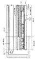
TFTの活性層のうち、チャネル形成領域およびその境界付近は特にTFTの電気特性を左右する重要な箇所であり、可能な限り不純物が存在しないことが望ましい。また、希ガス元素を添加した領域(ゲッタリングサイト)の境界にはニッケルシリサイドが偏析しやすい。そこで、本発明は、この境界をチャネル形成領域から離れた位置に配置することを最大の特徴としている。図1に示した例はレジストからなるマスクを用いてゲッタリングサイトの位置を設定し、nチャネル型TFTを作製した例である。
【0035】
図1(A)において、透光性を有する基板10はバリウムホウケイ酸ガラスやアルミノホウケイ酸ガラス、或いは石英などを用いることができる。まず、基板10の表面に、ブロッキング層11として無機絶縁膜を10〜200nmの厚さで形成する。好適なブロッキング層の一例は、プラズマCVD法で作製される酸化窒化シリコン膜であり、SiH4、NH3、N2Oから作製される第1酸化窒化シリコン膜を50nmの厚さに形成し、SiH4とN2Oから作製される第2酸化窒化珪素膜を100nmの厚さに形成したものが適用される。ブロッキング層11はガラス基板に含まれるアルカリ金属がこの上層に形成する半導体膜中に拡散しないために設けるものであり、石英を基板とする場合には省略することも可能である。
【0036】
次いで、ブロッキング層11上に半導体層を形成する。半導体層は、非晶質構造を有する半導体膜を公知の手段(スパッタ法、LPCVD法、またはプラズマCVD法等)により成膜した後、公知の結晶化処理(レーザー結晶化法、熱結晶化法、またはニッケルなどの触媒を用いた熱結晶化法等)を行って得られた結晶質半導体膜をフォトマスクを用いて所望の形状にパターニングして形成する。ここでは、ニッケルを用い、全面または一部に触媒含有層を塗布法、スパッタ法、蒸着法、またはプラズマ処理法によって形成した後、加熱処理または強光の照射を行い、結晶化を行う。この場合、結晶化は触媒となる金属元素が接した半導体膜の部分でシリサイドが形成され、それを核として結晶化が進行する。この半導体層の厚さは25〜80nm(好ましくは30〜60nm)の厚さで形成する。結晶質半導体膜の材料に限定はないが、好ましくはシリコンまたはシリコンゲルマニウム(SiGe)合金などで形成すると良い。
【0037】
次いで、半導体層を覆う絶縁膜14を形成する。絶縁膜14はプラズマCVD法またはスパッタ法を用い、厚さを40〜150nmとしてシリコンを含む絶縁膜の単層または積層構造で形成する。なお、この絶縁膜14はゲート絶縁膜となる。
【0038】
次いで、半導体層のうち、後にチャネル形成領域13aとなる領域を覆うレジストからなるマスク15を形成した後、絶縁膜14を通過させて半導体層に一導電型を付与する不純物元素(ドーパント、ここではリン)を低濃度に添加してP-領域12aを形成する。(図1(A))このP-領域12aの一部はLDD領域として機能するものである。
【0039】
次いで、マスク15を除去した後、絶縁膜14を間に挟んでP-領域12aと一部重なる電極16を形成する。(図1(B))この電極16としては、Ta、W、Ti、Mo、Al、Cu、Cr、Ndから選ばれた元素、または前記元素を主成分とする合金材料若しくは化合物材料で単層または積層を用いればよい。また、リン等の不純物元素をドーピングした多結晶シリコン膜に代表される半導体膜を用いてもよい。この電極16はゲート電極として機能する。
【0040】
次いで、レジストからなるマスク17を形成した後、絶縁膜14を通過させて半導体層に希ガス元素(Ar)を添加した後、半導体層に一導電型を付与する不純物元素(リン)を高濃度に添加してP++Ar領域18を形成する。(図1(C))希ガス元素としては、He、Ne、Ar、Kr、Xeから選ばれた一種または複数種を用いることができる。中でも安価なガスであるArを用いることが望ましい。添加方法としては、イオンドーピング法を用いてもよいし、イオン注入法を用いてもよい。また、先にリンを添加した後、アルゴンを添加してもよい。また、大気にふれることなく連続的にリンのドーピングとアルゴンのドーピングを行うことが望ましい。また、原料ガスとしてドーパント及び希ガス元素を含むガスを用いて、同一の工程で両方を添加してもよい。このP++Ar領域18は、後のゲッタリング工程でゲッタリングサイトとして機能する。なお、チャネル形成領域13aとP++Ar領域18との間にP-領域12bが形成される。
【0041】
次いで、マスク17を除去した後、ゲッタリングを行う。ゲッタリングは窒素雰囲気中で450〜800℃、1〜24時間、例えば550℃にて4時間の熱処理を行うと、図1(D)中の矢印の方向19、即ちチャネル形成領域13bからゲッタリングサイト18に金属元素を移動させることができる。このゲッタリングにより、絶縁層14で覆われた半導体膜、特にチャネル形成領域13bに含まれる金属元素を除去、または金属元素の濃度を低減する。また、このゲッタリングによりP-領域12bに含まれる金属元素も除去、または金属元素の濃度も低減する。このゲッタリングでは、条件によっては、希ガス元素によるゲッタリングと、リンによるゲッタリングとの相乗効果を得ることができる。また、熱処理に代えて強光を照射してもよい。また、熱処理に加えて強光を照射してもよい。ただし、ゲッタリングの加熱手段に、ハロゲンランプ、メタルハライドランプ、キセノンアークランプ、カーボンアークランプ、高圧ナトリウムランプ、または高圧水銀ランプから射出された光を用いるRTA法を用いる場合、半導体膜の加熱温度が400℃〜550℃となるように強光を照射することが望ましい。あまり高い加熱温度としてしまうと半導体膜中の歪みが無くなってしまい、ゲッタリングサイト(ニッケルシリサイド)からニッケルを飛び出させる作用やニッケルを捕獲する作用が消えてしまうため、ゲッタリング効率が低下してしまう。
【0042】
上記ゲッタリングによって、P-領域12bとP++Ar領域18との境界付近に金属元素が偏析しやすいものの、チャネル形成領域13bと間隔が離れているため、TFTの電気特性や信頼性等に影響を与えない。
【0043】
次いで、ドーパントを活性化するために加熱処理、強光の照射、またはレーザー光の照射を行えばよい。また、活性化と同時にゲート絶縁膜へのプラズマダメージやゲート絶縁膜と半導体層との界面へのプラズマダメージを回復することができる。特に、室温〜300℃の雰囲気中において、表面または裏面からYAGレーザーの第2高調波を照射してドーパントを活性化させることは非常に有効である。YAGレーザーはメンテナンスが少ないため好ましい。また、前の工程であるゲッタリング工程で活性化が可能であれば、同時に行ってもよい。
【0044】
以降の工程は、層間絶縁膜20a、20bを形成し、水素化を行って、P++Ar領域18に達するコンタクトホールを形成し、ソース電極21、ドレイン電極22をそれぞれ形成してTFTを完成させる。
【0045】
リンを用いたゲッタリングと比較して、希ガス元素の添加による本発明のゲッタリング能力は高く、さらに高濃度、例えば1×10²⁰〜5×10²¹/cm3で添加できるため、結晶化に用いる金属元素の添加量を多くすることができる。即ち、結晶化に用いる金属元素の添加量を多くすることによって結晶化の処理時間をさらに短時間で行うことが可能となる。また、結晶化の処理時間を変えない場合には、結晶化に用いる金属元素の添加量を多くすることによって、さらなる低温で結晶化することができる。また、結晶化に用いる金属元素の添加量を多くすることによって、自然核の発生を低減することができ、良好な結晶質半導体膜を形成することができる。
【0046】
また、希ガス元素を添加する処理時間は、1分または2分程度の短時間で高濃度の希ガス元素を半導体膜に添加することができるため、リンを用いたゲッタリングと比較してスループットが格段に向上する。
【0047】
なお、本発明は、上記工程順序(P-領域の形成→ゲート電極の形成→P++Ar領域の形成)に限定されず、P-領域の形成→P++Ar領域の形成→ゲート電極の形成という工程順序でもよければ、P++Ar領域の形成→P-領域の形成→ゲート電極の形成という工程順序でもよい。また、P++Ar領域の形成→P-領域の形成→ゲッタリング→活性化→ゲート電極の形成という工程順序としてもよい。このようにゲッタリング後でゲート電極を形成する場合には、ゲート電極として様々な材料、例えば高温に弱い低抵抗な材料(Cu、Al、Ag、Au等)を用いることが可能である。
【0048】
[実施の形態2]
また、図8に示した例は、電極をマスクとして自己整合的に希ガス元素またはドーパントを高濃度に添加した後、電極をエッチングしてテーパー部を形成し、そのテーパー部を通過させてドーパントを低濃度に行ってテーパー部に重なるLDD領域を形成した例である。
【0049】
実施の形態1と同様に絶縁膜34を形成する。基板30上にブロッキング層31、半導体層を形成して絶縁膜34を形成する。実施の形態1と同様にここでもニッケルを用いて結晶化を行う。
【0050】
次いで、次いで、絶縁膜34上に膜厚20〜100nmの第1の導電膜と、膜厚100〜400nmの第2の導電膜とを積層形成する。
【0051】
次いで、フォトリソグラフィ法を用いてレジストからなるマスク35aを形成し、電極36a、37aを形成するための第1のエッチング処理を行う。第1のエッチング条件として、ICP(Inductively Coupled Plasma:誘導結合型プラズマ)エッチング法を用いる。
【0052】
次いで、マスク35aを除去せずに、電極36a、37aをマスクとして第1のドーピングを行う。第1のドーピングでは、絶縁膜34を通過させて半導体層に希ガス元素(Ar)を添加した後、半導体層に一導電型を付与する不純物元素(リン)を高濃度に添加してP++Ar領域32aを形成する。(図8(A))なお、ドーピングされなかった領域を33aで示した。
【0053】
次いで、マスク35aをそのままの状態としたまま、第2のエッチング処理を行い、第2の導電層の一部を除去して電極37bを形成する。第2のエッチング処理によりマスク35aもエッチングされてマスク35bが形成される。一方、第1の導電層は、ほとんどエッチングされず、テーパー角の小さいテーパー部を有する電極36bを形成する。(図8(B))
【0054】
次いで、マスク35bを除去した後、第2のドーピング処理を行って図8(C)の状態を得る。ドーピングは電極37bを不純物元素に対するマスクとして用い、電極36bのテーパー部下方の半導体層に不純物元素が添加されるようにドーピングする。こうして、電極36bと重なるP-領域38を自己整合的に形成する。また、第2のドーピング処理では、P++Ar領域にもドーピングされ、P++Ar領域32bを形成する。なお、ドーピングされなかった領域(後にチャネル形成領域となる)を33bで示した。
【0055】
次いで、ゲッタリングを行う。ゲッタリングは窒素雰囲気中で450〜800℃、1〜24時間、例えば550℃にて14時間の熱処理を行うと、図8(D)中の矢印の方向39、即ちチャネル形成領域33cからゲッタリングサイト32bに金属元素を移動させることができる。このゲッタリングにより、絶縁層34で覆われた半導体膜、特にチャネル形成領域33cに含まれる金属元素を除去、または金属元素の濃度を低減する。また、このゲッタリングによりP-領域38bに含まれる金属元素も除去、または金属元素の濃度も低減する。また、熱処理に代えて強光を照射してもよい。また、熱処理に加えて強光を照射してもよい。
【0056】
次いで、ドーパントを活性化するために加熱処理、強光の照射、またはレーザー光の照射を行えばよい。また、活性化と同時にゲート絶縁膜へのプラズマダメージやゲート絶縁膜と半導体層との界面へのプラズマダメージを回復することができる。特に、室温〜300℃の雰囲気中において、表面または裏面からYAGレーザーの第2高調波を照射してドーパントを活性化させることは非常に有効である。YAGレーザーはメンテナンスが少ないため好ましい。また、前の工程であるゲッタリング工程で活性化が可能であれば、同時に行ってもよい。
【0057】
以降の工程は、層間絶縁膜40a、40bを形成し、水素化を行って、P++Ar領域32bに達するコンタクトホールを形成し、ソース電極41、ドレイン電極42をそれぞれ形成してTFTを完成させる。
【0058】
また、オフ電流を低減するために、電極36bのテーパー部のみを除去するエッチングを行ってもよい。
【0059】
また、高濃度のドーピングの際に用いるマスクと、希ガス元素のドーピングに用いるマスクとを同一マスクとした例を示したが、マスクを1枚増やして、それぞれに対応するマスクを形成してもよい。
【0060】
実施の形態1及び実施の形態2のいずれの場合も、絶縁膜を通過させて半導体層にリンを添加した例を示したが、絶縁膜を除去して半導体層の一部を露呈させた後にリンを添加してもよい。
【0061】
実施の形態1及び実施の形態2のいずれの場合もnチャネル型TFTを例に説明したが、リンに代えてボロンを用いればpチャネル型TFTを作製することができる。
【0062】
また、実施の形態1及び実施の形態2のいずれの場合もチャネル形成領域の境界にニッケルシリサイドが偏析しないように希ガス元素を添加する領域との間に間隔を有している。
【0063】
以上の構成でなる本発明について、以下に示す実施例でもってさらに詳細な説明を行うこととする。
【0064】
【実施例】
[実施例1]
本発明の実施形態を図2〜図6を用いて説明する。ここでは画素部の画素TFTと、画素部の周辺に設けられる駆動回路のTFTを同一基板上に作製する方法について工程に従って詳細に説明する。但し、説明を簡単にするために、駆動回路ではシフトレジスタ回路、バッファ回路などの基本回路であるCMOS回路と、サンプリング回路を形成するnチャネル型TFTとを図示することにする。なお、本実施例は、実施の形態1に示した作製工程に沿っている。
【0065】
図2(A)において、基板101には低アルカリガラス基板や石英基板を用いることができる。本実施例では低アルカリガラス基板を用いた。この場合、ガラス歪み点よりも10〜20℃程度低い温度であらかじめ熱処理しておいても良い。この基板101のTFTを形成する表面には、基板101からの不純物拡散を防ぐために、酸化シリコン膜、窒化シリコン膜または酸化窒化シリコン膜などの下地膜102を形成する。例えば、プラズマCVD法でSiH4、NH3、N2Oから作製される酸化窒化シリコン膜を100nm、同様にSiH4、N2Oから作製される酸化窒化シリコン膜を200nmの厚さに積層形成する。
【0066】
次に、20〜150nm(好ましくは30〜80nm)の厚さで非晶質構造を有する半導体膜103aを、プラズマCVD法やスパッタ法などの公知の方法で形成する。本実施例では、プラズマCVD法で非晶質シリコン膜を55nmの厚さに形成した。非晶質構造を有する半導体膜としては、非晶質半導体膜や微結晶半導体膜があり、非晶質シリコンゲルマニウム膜などの非晶質構造を有する化合物半導体膜を適用しても良い。また、下地膜102と非晶質シリコン膜103aとは同じ成膜法で形成することが可能であるので、両者を連続形成しても良い。下地膜を形成した後、一旦大気雰囲気に晒さないことでその表面の汚染を防ぐことが可能となり、作製するTFTの特性バラツキやしきい値電圧の変動を低減させることができる。(図2(A))
【0067】
そして、公知の結晶化技術を使用して非晶質シリコン膜103aから結晶質シリコン膜103bを形成する。例えば、レーザー結晶化法や熱結晶化法(固相成長法)を適用すれば良いが、ここでは、特開平7−130652号公報で開示された技術に従って、触媒元素を用いる結晶化法で結晶質シリコン膜103bを形成した。結晶化の工程に先立って、非晶質シリコン膜の含有水素量にもよるが、400〜500℃で1時間程度の熱処理を行い、含有水素量を5atom%以下にしてから結晶化させることが望ましい。非晶質シリコン膜を結晶化させると原子の再配列が起こり緻密化するので、作製される結晶質シリコン膜の厚さは当初の非晶質シリコン膜の厚さ(本実施例では55nm)よりも1〜15%程度減少した。(図2(B))
【0068】
そして、結晶質シリコン膜103bを島状に分割して、半導体層104〜107を形成する。その後、プラズマCVD法またはスパッタ法により50〜100nmの厚さの酸化シリコン膜によるマスク層108を形成する。(図2(C))
【0069】
そしてレジストマスク109を設け、nチャネル型TFTを形成する半導体層105〜107の全面にしきい値電圧を制御する目的で1×10¹⁶〜5×10¹⁷atoms/cm3程度の濃度でp型を付与する不純物元素としてボロン(B)を添加した。ボロン(B)の添加はイオンドープ法で実施しても良いし、非晶質シリコン膜を成膜するときに同時に添加しておくこともできる。ここでのボロン(B)添加は必ずしも必要でないが、ボロン(B)を添加した半導体層110〜112はnチャネル型TFTのしきい値電圧を所定の範囲内に収めるために形成することが好ましかった。(図2(D))
【0070】
駆動回路のnチャネル型TFTのLDD領域を形成するために、n型を付与する不純物元素を半導体層110、111に選択的に添加する。そのため、あらかじめレジストマスク113〜116を形成した。n型を付与する不純物元素としては、リン(P)や砒素(As)を用いれば良く、ここではリン(P)を添加すべく、フォスフィン(PH3)を用いたイオンドープ法を適用した。形成された不純物領域117、118のリン(P)濃度は2×10¹⁶〜5×10¹⁹atoms/cm3の範囲とすれば良い。本明細書中では、ここで形成された不純物領域117〜119に含まれるn型を付与する不純物元素の濃度を(n-)と表す。また、不純物領域119は、画素部の保持容量を形成するための半導体層であり、この領域にも同じ濃度でリン(P)を添加した。(図3(A))
【0071】
次に、マスク層108をフッ酸などにより除去する。また、図1(D)と図2(A)で添加した不純物元素を活性化させる工程を行ってもよい。活性化は、窒素雰囲気中で500〜600℃で1〜4時間の熱処理や、レーザー活性化の方法により行うことができる。また、両者を併用して行っても良い。
【0072】
そして、ゲート絶縁膜120をプラズマCVD法またはスパッタ法を用いて10〜150nmの厚さでシリコンを含む絶縁膜で形成する。例えば、120nmの厚さで酸化窒化シリコン膜を形成する。ゲート絶縁膜には、他のシリコンを含む絶縁膜を単層または積層構造として用いても良い。(図3(B))
【0073】
次に、ゲート電極を形成するために第1の導電層を成膜する。この第1の導電層は単層で形成しても良いが、必要に応じて二層あるいは三層といった積層構造としても良い。本実施例では、導電性の窒化物金属膜から成る導電層(A)121と金属膜から成る導電層(B)122とを積層させた。導電層(B)122はタンタル(Ta)、チタン(Ti)、モリブデン(Mo)、タングステン(W)から選ばれた元素、または前記元素を主成分とする合金か、前記元素を組み合わせた合金膜(代表的にはMo−W合金膜、Mo−Ta合金膜)で形成すれば良く、導電層(A)121は窒化タンタル(TaN)、窒化タングステン(WN)、窒化チタン(TiN)膜、窒化モリブデン(MoN)で形成する。また、導電層(A)121は代替材料として、タングステンシリサイド、チタンシリサイド、モリブデンシリサイドを適用しても良い。
【0074】
導電層(A)121は10〜50nm(好ましくは20〜30nm)とし、導電層(B)122は200〜400nm(好ましくは250〜350nm)とすれば良い。本実施例では、導電層(A)121に30nmの厚さの窒化タンタル膜を、導電層(B)122には350nmのTa膜を用い、いずれもスパッタ法で形成した。このスパッタ法による成膜では、スパッタ用のガスのArに適量のXeやKrを加えておくと、形成する膜の内部応力を緩和して膜の剥離を防止することができる。尚、図示しないが、導電層(A)121の下に2〜20nm程度の厚さでリン(P)をドープしたシリコン膜を形成しておくことは有効である。これにより、その上に形成される導電膜の密着性向上と酸化防止を図ると同時に、導電層(A)または導電層(B)が微量に含有するアルカリ金属元素がゲート絶縁膜120に拡散するのを防ぐことができる。(図3(C))
【0075】
次に、レジストマスク123〜127を形成し、導電層(A)121と導電層(B)122とを一括でエッチングしてゲート電極128〜131と容量配線132を形成する。ゲート電極128〜131と容量配線132は、導電層(A)から成る128a〜132aと、導電層(B)から成る128b〜132bとが一体として形成されている。この時、駆動回路に形成するゲート電極129、130は不純物領域117、118の一部と、ゲート絶縁膜120を介して重なるように形成する。(図3(D))
【0076】
次いで、駆動回路のpチャネル型TFTのソース領域およびドレイン領域を形成するために、p型を付与する不純物元素を添加する工程を行う。ここでは、ゲート電極128をマスクとして、自己整合的に不純物領域を形成する。このとき、nチャネル型TFTが形成される領域はレジストマスク133で被覆しておく。そして、ジボラン(B2H6)を用いたイオンドープ法で不純物領域134を形成した。この領域のボロン(B)濃度は3×10²⁰〜3×10²¹atoms/cm3となるようにする。本明細書中では、ここで形成された不純物領域134に含まれるp型を付与する不純物元素の濃度を(p+)と表す。(図4(A))
【0077】
次に、ゲッタリングサイトとなる領域の形成を行う。レジストのマスク135、136a、136b、137を形成し、希ガス元素を添加した。これはアルゴンガスを用いたイオンドープ法を用い、この領域のアルゴン濃度を1×10²⁰〜5×10²¹atoms/cm3とした。
【0078】
続いて、nチャネル型TFTにおいて、ソース領域またはドレイン領域として機能する不純物領域の形成を行う。レジストのマスク135、136a、136b、137をそのまま使用し、n型を付与する不純物元素を添加して不純物領域138〜142を形成した。これは、フォスフィン(PH3)を用いたイオンドープ法で行い、この領域のリン(P)濃度を1×10²⁰〜1×10²¹atoms/cm3とした。本明細書中では、ここで形成された不純物領域138〜142に含まれるn型を付与する不純物元素の濃度を(n+)と表す。(図4(B))
【0079】
不純物領域138〜142には、既に前工程で添加されたリン(P)またはボロン(B)が含まれているが、それに比して十分に高い濃度でリン(P)が添加されるので、前工程で添加されたリン(P)またはボロン(B)の影響は考えなくても良い。また、不純物領域138に添加されたリン(P)濃度は図4(A)で添加されたボロン(B)濃度の1/2〜1/3なのでp型の導電性が確保され、TFTの特性に何ら影響を与えることはなかった。
【0080】
そして、マスクを除去した後、画素部のnチャネル型TFTのLDD領域を形成するためのn型を付与する不純物添加の工程を行った。ここではゲート電極131をマスクとして自己整合的にn型を付与する不純物元素をイオンドープ法で添加した。添加するリン(P)の濃度は1×10¹⁶〜5×10¹⁸atoms/cm3であり、図3(A)および図4(A)と図4(B)で添加する不純物元素の濃度よりも低濃度で添加することで、実質的には不純物領域143、144のみが形成される。本明細書中では、この不純物領域143、144に含まれるn型を付与する不純物元素の濃度を(n--)と表す。(図4(C))
【0081】
次いで、ゲッタリングを行う。本実施例は、非晶質シリコン膜から金属元素を用いる結晶化の方法で作製したため、半導体層中には微量の金属元素が残留しており、少なくともチャネル形成領域の金属元素を除去または低減することが望ましい。この金属元素を除去する手段の一つにアルゴン(Ar)の添加によるゲッタリング作用を利用する。ゲッタリングは窒素雰囲気中で450〜800℃、1〜24時間、例えば550℃にて14時間の熱処理を行うと、金属元素が図4(D)中の矢印の方向に移動し、ゲッタリングサイトである不純物領域138〜142に金属元素を偏析させることができる。また、熱処理に代えて強光を照射してもよい。また、熱処理に加えて強光を照射してもよい。ただし、ゲッタリングの加熱手段に、ハロゲンランプ、メタルハライドランプ、キセノンアークランプ、カーボンアークランプ、高圧ナトリウムランプ、または高圧水銀ランプから射出された光を用いるRTA法を用いる場合、半導体膜の加熱温度が400℃〜550℃となるように強光を照射することが望ましい。あまり高い加熱温度としてしまうと半導体膜中の歪みが無くなってしまい、ゲッタリングサイト(ニッケルシリサイド)からニッケルを飛び出させる作用やニッケルを捕獲する作用が消えてしまうため、ゲッタリング効率が低下してしまう。
【0082】
次いで、それぞれの濃度で添加されたn型またはp型を付与する不純物元素を活性化する処理工程を行う。この工程はファーネスアニール法、レーザーアニール法、またはラピッドサーマルアニール法(RTA法)で行うことができる。ここでは裏面からYAGレーザーの第2高調波で活性化工程を行った。活性化により該不純物元素が添加された不純物領域とチャネル形成領域との接合を良好に形成することができた。
【0083】
次に、ゲート配線とする第2の導電膜を形成する。この第2の導電膜は低抵抗材料であるアルミニウム(Al)や銅(Cu)を主成分とする導電層(D)と、にチタン(Ti)やタンタル(Ta)、タングステン(W)、モリブデン(Mo)から成る導電層(E)とで形成すると良い。本実施例では、チタン(Ti)を0.1〜2重量%含むアルミニウム(Al)膜を導電層(D)145とし、チタン(Ti)膜を導電層(E)146として形成した。導電層(D)145は200〜400nm(好ましくは250〜350nm)とすれば良く、導電層(E)146は50〜200(好ましくは100〜150nm)で形成すれば良い。(図5(A))
【0084】
そして、ゲート電極に接続するゲート配線を形成するために導電層(E)146と導電層(D)145とをエッチング処理して、ゲート配線147、148と容量配線149を形成た。エッチング処理は最初にSiCl4とCl2とBCl3との混合ガスを用いたドライエッチング法で導電層(E)の表面から導電層(D)の途中まで除去し、その後リン酸系のエッチング溶液によるウエットエッチングで導電層(D)を除去することにより、下地との選択加工性を保ってゲート配線を形成することができた。
【0085】
次に、第1の層間絶縁膜150を形成する。第1の層間絶縁膜150は500〜1500nmの厚さで酸化シリコン膜または酸化窒化シリコン膜で形成され、その後、それぞれの半導体層に形成されたソース領域またはドレイン領域に達するコンタクトホールを形成し、ソース配線151〜154と、ドレイン配線155〜158を形成する。図示していないが、本実施例ではこの電極を、Ti膜を100nm、Tiを含むアルミニウム膜300nm、Ti膜150nmをスパッタ法で連続して形成した3層構造の積層膜とした。
【0086】
次に、パッシベーション膜159として、窒化シリコン膜または窒化酸化シリコン膜を50〜500nm(代表的には100〜300nm)の厚さで形成する。この状態で熱処理(300〜550℃で1〜12時間の熱処理)を行うと水素化を行うことができる。この工程はパッシベーション膜159に含まれる水素により半導体層のダングリングボンドを終端する工程である。第1の層間絶縁膜の存在に関係なく半導体層を水素化することができる。水素化の他の手段として、プラズマ水素化(プラズマにより励起された水素を用いる)を行っても良い。なお、ここで後に画素電極とドレイン配線を接続するためのコンタクトホールを形成する位置において、パッシベーション膜159に開口部を形成しておいても良い。(図5(C))
【0087】
その後、有機樹脂からなる第2の層間絶縁膜160を1.0〜1.5μmの厚さに形成する。有機樹脂としては、ポリイミド、アクリル、ポリアミド、ポリイミドアミド、BCB(ベンゾシクロブテン)等を使用することができる。ここでは、基板に塗布後、熱重合するタイプのポリイミドを用い、300℃で焼成して形成した。そして、第2の層間絶縁膜160にドレイン配線158に達するコンタクトホールを形成し、画素電極161を形成する。画素電極は、透過型液晶表示装置とする場合には透明導電膜を用いれば良く、反射型の液晶表示装置とする場合には反射率の高い金属膜を用いれば良い。本実施例では透過型の液晶表示装置とするために、酸化インジウム・スズ(ITO)膜を100nmの厚さにスパッタ法で形成した。(図6)
【0088】
こうして同一基板上に、駆動回路のTFTと画素部の画素TFTとを有した基板を完成させることができた。駆動回路にはCMOS回路を構成するpチャネル型TFT201と第1のnチャネル型TFT202、サンプリング回路を構成する第2のnチャネル型TFT203、画素部には画素TFT204、保持容量205が形成した。本明細書では便宜上このような基板をアクティブマトリクス基板と呼ぶ。
【0089】
駆動回路のpチャネル型TFT201には、半導体層104にチャネル形成領域206、ソース領域207a、207b、ドレイン領域208a,208bを有している。第1のnチャネル型TFT202には、半導体層105にチャネル形成領域209、LDD領域210、ソース領域211、ドレイン領域212を有している。このLDD領域210は、ドレイン領域側のみに形成され、ゲート電極129と重なる領域(以降、このようなLDD領域をLovと記す)とゲート電極129と重ならない領域(以降、このようなLDD領域をLoffと記す)とを両方とも有する。第2のnチャネル型TFT203には、半導体層106にチャネル形成領域213、LDD領域214,215、ソース領域216、ドレイン領域217を有している。このLDD領域214、215はLov領域とLoff領域とが形成されている。
【0090】
画素TFT204には、半導体層107にチャネル形成領域218、219、Loff領域220〜223、ソースまたはドレイン領域224〜226を有している。さらに、容量配線132、149と、ゲート絶縁膜と同じ材料から成る絶縁膜と、画素TFT204のドレイン領域226に接続し、n型を付与する不純物元素が添加された半導体層227とから保持容量205が形成されている。図6では画素TFT204をダブルゲート構造としたが、シングルゲート構造でも良いし、複数のゲート電極を設けたマルチゲート構造としても差し支えない。
【0091】
以上の様に本発明は、画素TFTおよび駆動回路が要求する仕様に応じて各回路を構成するTFTの構造を最適化し、半導体装置の動作性能と信頼性を向上させることを可能とすることができる。さらにゲート電極を耐熱性を有する導電性材料で形成することによりLDD領域やソース領域およびドレイン領域の活性化を容易とし、ゲート配線低抵抗材料で形成することにより、配線抵抗を十分低減できる。従って、画素部(画面サイズ)が4インチクラス以上の表示装置に適用することができる。
【0092】
[実施例2]
本実施例では、実施例1で作製したアクティブマトリクス基板から、アクティブマトリクス型液晶表示装置を作製する工程を以下に説明する。説明には図6を用いる。
【0093】
まず、実施例1に従い、図6の状態のアクティブマトリクス基板を得た後、図6のアクティブマトリクス基板上に配向膜を形成しラビング処理を行う。なお、本実施例では配向膜を形成する前に、アクリル樹脂膜等の有機樹脂膜をパターニングすることによって基板間隔を保持するための柱状のスペーサを所望の位置に形成した。また、柱状のスペーサに代えて、球状のスペーサを基板全面に散布してもよい。
【0094】
次いで、対向基板を用意する。この対向基板には、着色層、遮光層が各画素に対応して配置されたカラーフィルタが設けられている。また、駆動回路の部分にも遮光層を設けた。このカラーフィルタと遮光層とを覆う平坦化膜を設けた。次いで、平坦化膜上に透明導電膜からなる対向電極を画素部に形成し、対向基板の全面に配向膜を形成し、ラビング処理を施した。
【0095】
そして、画素部と駆動回路が形成されたアクティブマトリクス基板と対向基板とをシール材で貼り合わせる。シール材にはフィラーが混入されていて、このフィラーと柱状スペーサによって均一な間隔を持って2枚の基板が貼り合わせられる。その後、両基板の間に液晶材料を注入し、封止剤(図示せず)によって完全に封止する。液晶材料には公知の液晶材料を用いれば良い。このようにしてアクティブマトリクス型液晶表示装置が完成する。そして、必要があれば、アクティブマトリクス基板または対向基板を所望の形状に分断する。さらに、公知の技術を用いて偏光板等を適宜設けた。そして、公知の技術を用いてFPCを貼りつけた。
【0096】
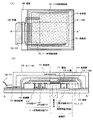
こうして得られた液晶モジュールの構成を図7の上面図を用いて説明する。
【0097】
図7で示す上面図は、画素部、駆動回路、FPC(フレキシブルプリント配線板:Flexible Printed Circuit)411を貼り付ける外部入力端子409、外部入力端子と各回路の入力部までを接続する配線410などが形成されたアクティブマトリクス基板と、カラーフィルタなどが設けられた対向基板400とがシール材407を介して貼り合わされている。
【0098】
ゲート配線側駆動回路301aと重なるように対向基板側に遮光層403aが設けられ、ソース配線側駆動回路301bと重なるように対向基板側に遮光層403bが形成されている。また、画素部302上の対向基板側に設けられたカラーフィルタ402は遮光層と、赤色(R)、緑色(G)、青色(B)の各色の着色層とが各画素に対応して設けられている。実際に表示する際には、赤色(R)の着色層、緑色(G)の着色層、青色(B)の着色層の3色でカラー表示を形成するが、これら各色の着色層の配列は任意なものとする。
【0099】
ここでは、カラー化を図るためにカラーフィルタ402を対向基板に設けているが特に限定されず、アクティブマトリクス基板を作製する際、アクティブマトリクス基板にカラーフィルタを形成してもよい。
【0100】
また、カラーフィルタにおいて隣り合う画素の間には遮光層が設けられており、表示領域以外の箇所を遮光している。また、ここでは、駆動回路を覆う領域にも遮光層403a、403bを設けているが、駆動回路を覆う領域は、後に液晶表示装置を電子機器の表示部として組み込む際、カバーで覆うため、特に遮光層を設けない構成としてもよい。また、アクティブマトリクス基板を作製する際、アクティブマトリクス基板に遮光層を形成してもよい。
【0101】
また、上記遮光層を設けずに、対向基板と対向電極の間に、カラーフィルタを構成する着色層を複数層重ねた積層で遮光するように適宜配置し、表示領域以外の箇所(各画素電極の間隙)や、駆動回路を遮光してもよい。
【0102】
また、外部入力端子にはベースフィルムと配線から成るFPC411が異方性導電性樹脂で貼り合わされている。さらに補強板で機械的強度を高めている。
【0103】
以上のようにして作製される液晶モジュールは各種電子機器の表示部として用いることができる。
【0104】
[実施例3]
本実施例は、実施例1と異なるTFT構造としてアクティブマトリクス基板を作製した例について図9〜11に示す。なお、本実施例は、実施の形態2に示した作製工程に沿っている。
【0105】
まず、本実施例ではコーニング社の#7059ガラスや#1737ガラスなどに代表されるバリウムホウケイ酸ガラス、またはアルミノホウケイ酸ガラスなどのガラスからなる基板500を用いる。なお、基板500としては、透光性を有する基板であれば限定されず、石英基板を用いても良い。また、本実施例の処理温度に耐えうる耐熱性を有するプラスチック基板を用いてもよい。
【0106】
次いで、基板500上に酸化シリコン膜、窒化シリコン膜または酸化窒化シリコン膜などの絶縁膜から成る下地膜501を形成する。本実施例では下地膜501として2層構造を用いるが、前記絶縁膜の単層膜または2層以上積層させた構造を用いても良い。本実施例では、膜厚50nmの酸化窒化シリコン膜501a、膜厚100nmの酸化窒化シリコン膜501bを形成した。
【0107】
次いで、下地膜上に半導体層502〜506を形成する。この半導体層502〜506の厚さは25〜80nm(好ましくは30〜60nm)の厚さで形成する。結晶質半導体膜の材料に限定はないが、好ましくはシリコンまたはシリコンゲルマニウム(SiXGe1-X(X=0.0001〜0.02))合金などで形成すると良い。本実施例では、プラズマCVD法を用い、55nmの非晶質シリコン膜を成膜した後、ニッケルを含む溶液を非晶質シリコン膜上に保持させた。この非晶質シリコン膜に脱水素化(500℃、1時間)を行った後、熱結晶化(550℃、4時間)を行い、さらに結晶化を改善するためのレーザーアニ―ル処理を行って結晶質シリコン膜を形成し、所望の形状にパターニングした。
【0108】
次いで、半導体層502〜506の表面をバッファーフッ酸等のフッ酸系のエッチャントで洗浄した後、プラズマCVD法またはスパッタ法を用い、厚さを40〜150nmとして珪素を主成分とする絶縁膜507を形成する。
【0109】
次いで、図9(A)に示すように、ゲート絶縁膜507上に膜厚20〜100nmの第1の導電膜508と、膜厚100〜400nmの第2の導電膜509とを積層形成する。本実施例では、膜厚30nmのTaN膜からなる第1の導電膜508と、膜厚370nmのW膜からなる第2の導電膜509を積層形成した。
【0110】
なお、本実施例では、第1の導電膜508をTaN、第2の導電膜509をWとしたが、特に限定されず、いずれもTa、W、Ti、Mo、Al、Cu、Cr、Ndから選ばれた元素、または前記元素を主成分とする合金材料若しくは化合物材料で単層または積層を用いればよい。また、リン等の不純物元素をドーピングした多結晶シリコン膜に代表される半導体膜を用いてもよい。また、AgPdCu合金を用いてもよい。また、第1の導電膜をタンタル(Ta)膜で形成し、第2の導電膜をW膜とする組み合わせ、第1の導電膜を窒化チタン(TiN)膜で形成し、第2の導電膜をW膜とする組み合わせ、第1の導電膜を窒化タンタル(TaN)膜で形成し、第2の導電膜をAl膜とする組み合わせ、第1の導電膜を窒化タンタル(TaN)膜で形成し、第2の導電膜をCu膜とする組み合わせとしてもよい。
【0111】
次に、フォトリソグラフィ法を用いてレジストからなるマスク510〜515を形成し、電極及び配線を形成するための第1のエッチング処理を行う。第1のエッチング処理では第1及び第2のエッチング条件で行う。本実施例では第1のエッチング条件として、ICP(Inductively Coupled Plasma:誘導結合型プラズマ)エッチング法を用い、エッチング用ガスにCF4とCl2とO2とを用い、それぞれのガス流量比を25/25/10(sccm)とし、1Paの圧力でコイル型の電極に500WのRF(13.56MHz)電力を投入してプラズマを生成してエッチングを行った。なお、エッチング用ガスとしては、Cl2、BCl3、SiCl4、CCl4などを代表とする塩素系ガスまたはCF4、SF6、NF3などを代表とするフッ素系ガス、またはO2を適宜用いることができる。ここでは、松下電器産業(株)製のICPを用いたドライエッチング装置(Model E645−□ICP)を用いた。基板側(試料ステージ)にも150WのRF(13.56MHz)電力を投入し、実質的に負の自己バイアス電圧を印加する。この第1のエッチング条件によりW膜をエッチングして第1の導電層の端部をテーパー形状とする。第1のエッチング条件でのWに対するエッチング速度は200.39nm/min、TaNに対するエッチング速度は80.32nm/minであり、TaNに対するWの選択比は約2.5である。また、この第1のエッチング条件によって、Wのテーパー角は、約26°となる。
【0112】
この後、レジストからなるマスク510〜515を除去せずに第2のエッチング条件に変え、エッチング用ガスにCF4とCl2とを用い、それぞれのガス流量比を30/30(sccm)とし、1Paの圧力でコイル型の電極に500WのRF(13.56MHz)電力を投入してプラズマを生成して約30秒程度のエッチングを行った。基板側(試料ステージ)にも20WのRF(13.56MHz)電力を投入し、実質的に負の自己バイアス電圧を印加する。CF4とCl2を混合した第2のエッチング条件ではW膜及びTaN膜とも同程度にエッチングされる。第2のエッチング条件でのWに対するエッチング速度は58.97nm/min、TaNに対するエッチング速度は66.43nm/minである。なお、ゲート絶縁膜上に残渣を残すことなくエッチングするためには、10〜20%程度の割合でエッチング時間を増加させると良い。
【0113】
上記第1のエッチング処理では、レジストからなるマスクの形状を適したものとすることにより、基板側に印加するバイアス電圧の効果により第1の導電層及び第2の導電層の端部がテーパー形状となる。このテーパー部の角度は15〜45°とすればよい。
【0114】
こうして、第1のエッチング処理により第1の導電層と第2の導電層から成る第1の形状の導電層516〜521(第1の導電層516a〜521aと第2の導電層516b〜521b)を形成する。
【0115】
そして、レジストからなるマスクを除去せずに第1のドーピング処理を行い、半導体層に希ガス元素とn型を付与する不純物元素とを添加する。(図9(B))ドーピング処理はイオンドープ法、若しくはイオン注入法で行えば良い。ここでは、希ガス元素としてアルゴンを用い、ドーピングガスとしてアルゴンガス100%としたイオンドープ法を用いて添加した後、大気にふれることなくn型を付与する不純物元素としてリンを用い、フォスフィン(PH3)5%水素希釈ガスとしたイオンドープ法を用いて添加する。
【0116】
この場合、導電層516〜521がn型を付与する不純物元素に対するマスクとなり、自己整合的にゲッタリングサイトとしても機能する高濃度不純物領域522〜533が形成される。高濃度不純物領域522〜533には1×10²⁰〜5×10²¹/cm3の濃度範囲でアルゴンを添加し、さらに、3×1019〜3×1020/cm3の濃度範囲でn型を付与する不純物元素とを添加する。
【0117】
また、第1のドーピング処理では、リンを添加した後、アルゴンを添加してもよい。また、第1のドーピング処理としてフォスフィンを含む希ガスを原料ガスとし、半導体膜にリン元素と希ガス元素とを同一工程で添加してもよい。
【0118】
次いで、レジストからなるマスクを除去せずに第2のエッチング処理を行う。ここでは、エッチング用ガスにSF6とCl2とO2とを用い、それぞれのガス流量比を24/12/24(sccm)とし、1.3Paの圧力でコイル型の電極に700WのRF(13.56MHz)電力を投入してプラズマを生成してエッチングを25秒行った。基板側(試料ステージ)にも10WのRF(13.56MHz)電力を投入し、実質的に負の自己バイアス電圧を印加する。第2のエッチング処理でのWに対するエッチング速度は227.3nm/min、TaNに対するエッチング速度は32.1nm/minであり、TaNに対するWの選択比は7.1であり、絶縁膜507であるSiONに対するエッチング速度は33.7nm/minであり、TaNに対するWの選択比は6.83である。このようにエッチングガス用ガスにSF6を用いた場合、絶縁膜507との選択比が高いので膜減りを抑えることができる。また、駆動回路のTFTにおいては、テーパ−部のチャネル長方向の幅が長ければ長いほど信頼性が高いため、テーパ−部を形成する際、SF6を含むエッチングガスでドライエッチングを行うことが有効である。
【0119】
この第2のエッチング処理によりWのテーパー角は70°となった。この第2のエッチング処理により第2の導電層534b〜539bを形成する。一方、第1の導電層は、ほとんどエッチングされず、第1の導電層534a〜539aを形成する。また、上記第2のエッチング処理において、CF4とCl2とO2とをエッチングガスに用いることも可能である。
【0120】
次いで、レジストからなるマスクを除去した後、第2のドーピング処理を行って図9(C)の状態を得る。ドーピングは第2の導電層534b〜539bを不純物元素に対するマスクとして用い、第1の導電層のテーパー部下方の半導体層に不純物元素が添加されるようにドーピングする。本実施例では、不純物元素としてP(リン)を用い、ドーピング条件をドーズ量1.5×10¹⁴/cm2、加速電圧90keV、イオン電流密度0.5μA/cm2、フォスフィン(PH3)5%水素希釈ガス、ガス流量30sccmにてプラズマドーピングを行った。こうして、第1の導電層と重なる低濃度不純物領域541〜554を自己整合的に形成する。この低濃度不純物領域541〜554へ添加されたリン(P)の濃度は、1×1017〜1×1019/cm3であり、且つ、第1の導電層のテーパー部の膜厚に従って濃度勾配を有している。なお、第1の導電層のテーパー部と重なる半導体層において、第1の導電層のテーパー部の端部から内側に向かって不純物濃度(P濃度)が次第に低くなっている。また、高濃度不純物領域522〜533にも不純物元素が添加され、高濃度不純物領域555〜566を形成する。
【0121】
次いで、後にnチャネル型TFTの活性層となる半導体層をレジストからなるマスク567〜569で覆い、第3のドーピング処理を行う。この第3のドーピング処理により、pチャネル型TFTの活性層となる半導体層に前記一導電型(n型)とは逆の導電型(p型)を付与する不純物元素が添加されたp型不純物領域570〜573(高濃度不純物領域570a〜573a及び低濃度不純物領域570b〜573b)を形成する。(図10(A))不純物領域570a〜573aにはそれぞれ異なる濃度でリンが添加されているが、そのいずれの領域においてもボロンの濃度が6×10¹⁹〜6×10²⁰/cm3となるようにドーピング処理することにより、pチャネル型TFTのソース領域およびドレイン領域として機能するために何ら問題は生じない。
【0122】
次いで、レジストからなるマスク574を形成して第3のエッチング処理を行う。この第3のエッチング処理では第1の導電層のテーパー部のみを選択的にエッチングする。第3のエッチング処理は、エッチングガスにWとの選択比が高いCl3を用い、ICPエッチング装置を用いて行う。第3のエッチングにより、第1の導電層537c〜539cが形成される。(図10(B))
【0123】
上記第3のエッチング処理によって、画素部には、第1の導電層537c〜539cと重ならず、濃度勾配を有する低濃度不純物領域(LDD領域)547〜554が形成される。なお、駆動回路において、低濃度不純物領域(GOLD領域)541〜546は、第1の導電層534a〜536aと重なったままである。このように、各回路に応じてTFTの構造を作り分けている。
【0124】
また、本実施例では第3のドーピング処理の後に、第3のエッチング処理を行った例を示したが、第3のエッチング処理を行った後に第3のドーピング処理を行ってもよい。
【0125】
次いで、レジストからなるマスク574を除去して、ゲッタリング処理を行う。ゲッタリングは窒素雰囲気中で450〜800℃、1〜24時間、例えば550℃にて4時間の熱処理を行うと、図10(C)中の矢印の方向、即ちチャネル形成領域からゲッタリングサイトに金属元素を移動させることができる。このゲッタリングにより、絶縁膜を間に挟んで第1の導電層と重なる半導体膜、特にチャネル形成領域に含まれる金属元素を除去、または金属元素の濃度を低減する。このゲッタリングでは、条件によっては、希ガス元素によるゲッタリングと、リンによるゲッタリングとの相乗効果を得ることができる。また、熱処理に代えて強光を照射してもよい。また、熱処理に加えて強光を照射してもよい。ただし、ゲッタリングの加熱手段に、ハロゲンランプ、メタルハライドランプ、キセノンアークランプ、カーボンアークランプ、高圧ナトリウムランプ、または高圧水銀ランプから射出された光を用いるRTA法を用いる場合、半導体膜の加熱温度が400℃〜550℃となるように強光を照射することが望ましい。あまり高い加熱温度としてしまうと半導体膜中の歪みが無くなってしまい、ゲッタリングサイト(ニッケルシリサイド)からニッケルを飛び出させる作用やニッケルを捕獲する作用が消えてしまうため、ゲッタリング効率が低下してしまう。
【0126】
さらに、ゲッタリングの条件によっては、ゲッタリングと同時に不純物元素(リン、ボロン)を活性化することもできる。
【0127】
次いで、第1の層間絶縁膜575を形成する。この第1の層間絶縁膜575としては、プラズマCVD法またはスパッタ法を用い、厚さを10〜200nmとしてシリコンを含む絶縁膜で形成する。
【0128】
次いで、図10(D)に示すように、それぞれの半導体層に添加された不純物元素を活性化処理する工程を行う。この活性化工程はYAGレーザーまたはエキシマレーザーを裏面から照射することによって行う。裏面から照射することによって、ゲート電極と絶縁膜を介して重なる不純物領域の活性化を行うことができる。
【0129】
また、本実施例では、上記活性化の前に第1の層間絶縁膜を形成した例を示したが、上記活性化を行った後、第1の層間絶縁膜を形成する工程としてもよい。
【0130】
次いで、窒化シリコン膜からなる第2の層間絶縁膜576を形成して熱処理(300〜550℃で1〜12時間の熱処理)を行い、半導体層を水素化する工程を行う。本実施例では、窒素雰囲気中で410℃、1時間の熱処理を行った。この工程は第2の層間絶縁膜576に含まれる水素により半導体層のダングリングボンドを終端する工程である。第1の層間絶縁膜の存在に関係なく半導体層を水素化することができる。水素化の他の手段として、プラズマ水素化(プラズマにより励起された水素を用いる)を行っても良い。
【0131】
次いで、第2の層間絶縁膜576上に有機絶縁物材料から成る第3の層間絶縁膜277を形成する。本実施例では膜厚1.6μmのアクリル樹脂膜を形成した。次いで、各不純物領域(557、558、561〜563、565、570a、571a、572a、573a)に達するコンタクトホールを形成するためのパターニングを行う。本実施例では複数のエッチング処理を行った。本実施例では第2の層間絶縁膜をエッチングストッパーとして第3の層間絶縁膜をエッチングした後、第1の層間絶縁膜をエッチングストッパーとして第2の層間絶縁膜をエッチングしてから第1の層間絶縁膜をエッチングした。
【0132】
次いで、不純物領域(557、558、561〜563、570a、571a、572a、573a)とそれぞれ電気的に接続する電極578〜586と、不純物領域565と電気的に接続する画素電極587を形成する。これらの電極及び画素電極の材料は、AlまたはAgを主成分とする膜、またはそれらの積層膜等の反射性の優れた材料を用いる。
【0133】
以上の様にして、nチャネル型TFT606及びpチャネル型TFT605からなるロジック回路部603と、nチャネル型TFT608及びpチャネル型TFT607からなるサンプリング回路部604とを有する駆動回路601と、nチャネルTFT609からなる画素TFT及び保持容量610とを有する画素部602とを同一基板上に形成することができる。
【0134】
なお、本実施例ではnチャネル型TFT609は、ソース領域およびドレイン領域の間に二つのチャネル形成領域を有した構造(ダブルゲート構造)となっているが、本実施例はダブルゲート構造に限定されることなく、チャネル形成領域が一つ形成されるシングルゲート構造もしくは三つ形成されるトリプルゲート構造であっても良い。
【0135】
また、本実施例では、希ガス元素を多量に添加したため、下地膜及び基板にも添加される。希ガス元素は、下地膜及び基板のうち、電極516〜521で覆われた領域以外の領域、即ちチャネル形成領域588〜593および低濃度不純物領域以外の領域に位置する下地膜中あるいは基板中に添加される。
【0136】
[実施例4]
実施例3では画素電極が反射性を有する金属材料で形成された反射型の表示装置の例を示したが、本実施例では画素電極を透光性を有する導電膜で形成した透過型の表示装置の例を図12に示す。
【0137】
層間絶縁膜800を形成する工程までは実施例3と同じであるので、ここでは省略する。実施例1に従って層間絶縁膜577を形成した後、透光性を有する導電膜からなる画素電極801を形成する。透光性を有する導電膜としては、ITO(酸化インジウム酸化スズ合金)、酸化インジウム酸化亜鉛合金(In2O3―ZnO)、酸化亜鉛(ZnO)等を用いればよい。
【0138】
その後、層間絶縁膜800にコンタクトホールを形成する。次いで、画素電極801と重なる接続電極802を形成する。この接続電極802は、コンタクトホールを通じてドレイン領域と接続されている。また、この接続電極802と同時に他のTFTのソース電極またはドレイン電極も形成する。
【0139】
また、ここでは全ての駆動回路を基板上に形成した例を示したが、駆動回路の一部に数個のICを用いてもよい。
【0140】
以上のようにしてアクティブマトリクス基板が形成される。このアクティブマトリクス基板を用い、実施例2に従って液晶モジュールを作製し、バックライト804、導光板805を設け、カバー806で覆えば、図14に示すアクティブマトリクス型液晶表示装置が完成する。なお、カバー806と液晶モジュールは接着剤や有機樹脂を用いて貼り合わせる。また、基板と対向基板を貼り合わせる際、枠で囲んで有機樹脂を枠と基板との間に充填して接着してもよい。また、透過型であるので偏光板803は、アクティブマトリクス基板と対向基板の両方に貼り付ける。
【0141】
なお、本実施例は実施例3と組み合わせることが可能である。
【0142】
[実施例5]
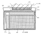
本実施例では、EL(Electro Luminescence)素子を備えた発光表示装置を作製する例を図13に示す。
【0143】
図13(A)は、ELモジュールをを示す上面図、図13(B)は図13(A)をA−A’で切断した断面図である。絶縁表面を有する基板700(例えば、ガラス基板、結晶化ガラス基板等)に、画素部702、ソース側駆動回路701、及びゲート側駆動回路703を形成する。これらの画素部や駆動回路は、実施の形態に従えば得ることができる。また、718はシール材、719はDLC膜であり、画素部および駆動回路部はシール材718で覆われ、そのシール材は保護膜719で覆われている。さらに、接着材を用いてカバー材720で封止されている。熱や外力などによる変形に耐えるためカバー材720は基板700と同じ材質のもの、例えばガラス基板を用いることが望ましく、サンドブラスト法などにより図13に示す凹部形状(深さ3〜10μm)に加工する。さらに加工して乾燥剤721が設置できる凹部(深さ50〜200μm)を形成することが望ましい。また、多面取りでELモジュールを製造する場合、基板とカバー材とを貼り合わせた後、CO2レーザー等を用いて端面が一致するように分断してもよい。
【0144】
なお、708はソース側駆動回路701及びゲート側駆動回路703に入力される信号を伝送するための配線であり、外部入力端子となるFPC(フレキシブルプリントサーキット)709からビデオ信号やクロック信号を受け取る。なお、ここではFPCしか図示されていないが、このFPCにはプリント配線基盤(PWB)が取り付けられていても良い。本明細書における発光装置には、発光装置本体だけでなく、それにFPCもしくはPWBが取り付けられた状態をも含むものとする。
【0145】
次に、断面構造について図13(B)を用いて説明する。基板500上に絶縁膜710が設けられ、絶縁膜710の上方には画素部702、ゲート側駆動回路503が形成されており、画素部702は電流制御用TFT711とそのドレインに電気的に接続された画素電極712を含む複数の画素により形成される。また、ゲート側駆動回路703はnチャネル型TFT713とpチャネル型TFT714とを組み合わせたCMOS回路を用いて形成される。
【0146】
これらのTFT(711、713、714を含む)は、実施の形態または実施例1、実施例3に従って作製すればよい。
【0147】
画素電極712はEL素子の陽極として機能する。また、画素電極712の両端にはバンク715が形成され、画素電極712上にはEL層716およびEL素子の陰極717が形成される。
【0148】
EL層716としては、発光層、電荷輸送層または電荷注入層を自由に組み合わせてEL層(発光及びそのためのキャリアの移動を行わせるための層)を形成すれば良い。例えば、低分子系有機EL材料や高分子系有機EL材料を用いればよい。また、EL層として一重項励起により発光(蛍光)する発光材料(シングレット化合物)からなる薄膜、または三重項励起により発光(リン光)する発光材料(トリプレット化合物)からなる薄膜を用いることができる。また、電荷輸送層や電荷注入層として炭化珪素等の無機材料を用いることも可能である。これらの有機EL材料や無機材料は公知の材料を用いることができる。
【0149】
陰極717は全画素に共通の配線としても機能し、接続配線708を経由してFPC709に電気的に接続されている。さらに、画素部702及びゲート側駆動回路703に含まれる素子は全て陰極717、シール材718、及び保護膜719で覆われている。
【0150】
なお、シール材718としては、できるだけ可視光に対して透明もしくは半透明な材料を用いるのが好ましい。また、シール材718はできるだけ水分や酸素を透過しない材料であることが望ましい。
【0151】
また、シール材718を用いて発光素子を完全に覆った後、すくなくとも図13に示すようにDLC膜等からなる保護膜719をシール材718の表面(露呈面)に設けることが好ましい。また、基板の裏面を含む全面に保護膜を設けてもよい。ここで、外部入力端子(FPC)が設けられる部分に保護膜が成膜されないように注意することが必要である。マスクを用いて保護膜が成膜されないようにしてもよいし、CVD装置でマスキングテープとして用いるテフロン等のテープで外部入力端子部分を覆うことで保護膜が成膜されないようにしてもよい。
【0152】
以上のような構造でEL素子をシール材718及び保護膜で封入することにより、EL素子を外部から完全に遮断することができ、外部から水分や酸素等のEL層の酸化による劣化を促す物質が侵入することを防ぐことができる。従って、信頼性の高い発光装置を得ることができる。
【0153】
また、画素電極を陰極とし、EL層と陽極を積層して図13とは逆方向に発光する構成としてもよい。図14にその一例を示す。なお、上面図は同一であるので省略する。
【0154】
図14に示した断面構造について以下に説明する。基板1000としては、ガラス基板や石英基板の他にも、半導体基板または金属基板も使用することができる。基板1000上に絶縁膜1010が設けられ、絶縁膜1010の上方には画素部1002、ゲート側駆動回路1003が形成されており、画素部1002は電流制御用TFT1011とそのドレインに電気的に接続された画素電極1012を含む複数の画素により形成される。また、ゲート側駆動回路1003はnチャネル型TFT1013とpチャネル型TFT1014とを組み合わせたCMOS回路を用いて形成される。
【0155】
画素電極1012はEL素子の陰極として機能する。また、画素電極1012の両端にはバンク1015が形成され、画素電極1012上にはEL層1016およびEL素子の陽極1017が形成される。
【0156】
陽極1017は全画素に共通の配線としても機能し、接続配線1008を経由してFPC1009に電気的に接続されている。さらに、画素部1002及びゲート側駆動回路1003に含まれる素子は全て陽極1017、シール材1018、及びDLC等からなる保護膜1019で覆われている。また、カバー材1021と基板1000とを接着剤で貼り合わせた。また、カバー材には凹部を設け、乾燥剤1021を設置する。
【0157】
なお、シール材1018としては、できるだけ可視光に対して透明もしくは半透明な材料を用いるのが好ましい。また、シール材1018はできるだけ水分や酸素を透過しない材料であることが望ましい。
【0158】
また、図14では、画素電極を陰極とし、EL層と陽極を積層したため、発光方向は図14に示す矢印の方向となっている。
【0159】
なお、本実施例は実施例1乃至4のいずれか一と組み合わせることが可能である。
【0160】
[実施例6]
実施例1では、トップゲート型TFTを例に説明したが、本発明は図15に示すボトムゲート型TFTにも適用することができる。
【0161】
図15(A)は、画素部の画素の一つを拡大した上面図であり、図15(A)において、点線A−A'で切断した部分が、図15(B)の画素部の断面構造に相当する。
【0162】
図15に示す画素部において、画素TFT部はNチャネル型TFTで形成されている。基板上51にゲート電極52が形成され、その上に窒化珪素からなる第1絶縁膜53a、酸化珪素からなる第2絶縁膜53bが設けられている。また、第2絶縁膜上には、活性層としてソース領域またはドレイン領域54〜56と、チャネル形成領域57、58と、前記ソース領域またはドレイン領域とチャネル形成領域の間にLDD領域59、60が形成される。また、チャネル形成領域57、58は絶縁層61、62で保護される。絶縁層61、62及び活性層を覆う第1の層間絶縁膜63にコンタクトホールを形成した後、ソース領域54に接続する配線64が形成され、ドレイン領域56に配線65が接続され、さらにその上にパッシベーション膜66が形成される。そして、その上に第2の層間絶縁膜67が形成される。さらに、その上に第3の層間絶縁膜68が形成され、ITO、SnO2等の透明導電膜からなる画素電極69が配線65と接続される。また、70は画素電極69と隣接する画素電極である。
【0163】
本実施例では、実施の形態1に従って、ソース領域またはドレイン領域54〜56に希ガス元素を添加してゲッタリングを行ったチャネル形成領域57、58を備えている。
【0164】
本実施例では一例としてチャネルストップ型のボトムゲート型のTFTの例を示したが特に限定されない。
【0165】
なお、本実施例では、画素部の画素TFTのゲート配線をダブルゲート構造としているが、オフ電流のバラツキを低減するために、トリプルゲート構造等のマルチゲート構造としても構わない。また、開口率を向上させるためにシングルゲート構造としてもよい。
【0166】
また、画素部の容量部は、第1絶縁膜及び第2絶縁膜を誘電体として、容量配線71と、ドレイン領域56とで形成されている。
【0167】
なお、図15で示した画素部はあくまで一例に過ぎず、特に上記構成に限定されないことはいうまでもない。
【0168】
なお、本実施例は実施例1乃至5のいずれか一と組み合わせることが可能である。
【0169】
[実施例7]
本実施例は、金属元素を添加した後、マスクを形成し、希ガス元素を添加してゲッタリングを行った後、半導体膜のパターニングを行った後、再度希ガス元素を添加して実施の形態1と同様のゲッタリングを行う例を示す。
【0170】
実施の形態1に従って、金属元素を添加して結晶化を行う。その後、本実施例では酸化シリコン膜からなる第1マスクを形成し、希ガス元素を添加してゲッタリングサイトを形成する。この第1マスクは、ゲッタリングのためのものであり、帯状の開口部を有するマスクであってもよいし、後に行われる半導体層のパターニングに用いるマスクより表面積が大きいものを用いる。次いで、熱処理または強光の照射を行ってゲッタリングを行う。ゲッタリングは窒素雰囲気中で450〜800℃、1〜24時間、例えば550℃にて14時間の熱処理を行うと、ゲッタリングサイトに金属元素を偏析させることができる。次いで、半導体層のパターニングを行う。この時のパターニングに使用する第2マスクは半導体膜をパターニングするためのものであり、第1マスクよりも小さく、且つ内側に形成する。このパターニングにより、ゲッタリングサイトは除去され、さらにゲッタリングサイトの境界近傍の半導体も除去する。ゲッタリングを行うと、金属元素が希ガス元素を添加した領域の境界に偏析しやすい傾向があることから、希ガス元素を添加した領域付近の半導体膜も除去する。こうして、結晶構造を有する半導体層を形成する。以降の工程は、実施の形態1に従えばよい。
【0171】
従って、本実施例では、工程数およびマスク数が増加するものの、2回のゲッタリングが行われるため、さらにチャネル形成領域に含まれる金属元素を低減することができる。本実施例では、2回のゲッタリングを行う例を示したが特に限定されず、2回以上のゲッタリングを行ってもよい。また、他の公知のゲッタリング方法と組み合わせてもよいことはいうまでもない。
【0172】
なお、本実施例は実施例1乃至6のいずれか一と組み合わせることが可能である。
【0173】
[実施例8]
本実施例では、実施例3と異なるプロセスでアクティブマトリクス基板を作製した例について図16〜18に示す。
【0174】
本実施例は、基板1600上に下地膜1600(酸化窒化シリコン膜1601a、酸化窒化シリコン膜1601bの積層)を設け、その上に半導体層1602〜1606を形成し、絶縁膜1607を形成し、該絶縁膜上に第1の導電膜1608と、第2の導電膜1609とを積層形成する工程は、実施例3と同一である。従って、詳しい説明はここでは省略する。なお、図16(A)は、図9(A)と同じ状態を示している。
【0175】
次いで、実施例3と同様な方法で第1のエッチング処理を行い、第1の導電層と第2の導電層から成る第1の形状の導電層1616〜1621(第1の導電層1616a〜1621aと第2の導電層1616b〜1621b)を形成する。(図16(B))なお、この工程までが実施例3と同一である。
【0176】
そして、本実施例は、第1のエッチング処理に引き続き、レジストからなるマスクを除去せずに第2のエッチング処理を行う。ここでは、エッチング用ガスにSF6とCl2とO2とを用い、それぞれのガス流量比を24/12/24(sccm)とし、1.3Paの圧力でコイル型の電極に700WのRF(13.56MHz)電力を投入してプラズマを生成してエッチングを25秒行った。基板側(試料ステージ)にも10WのRF(13.56MHz)電力を投入し、実質的に負の自己バイアス電圧を印加する。第2のエッチング処理でのWに対するエッチング速度は227.3nm/min、TaNに対するエッチング速度は32.1nm/minであり、TaNに対するWの選択比は7.1であり、絶縁膜1607であるSiONに対するエッチング速度は33.7nm/minであり、TaNに対するWの選択比は6.83である。このようにエッチングガス用ガスにSF6を用いた場合、絶縁膜1607との選択比が高いので膜減りを抑えることができる。また、駆動回路のTFTにおいては、テーパ−部のチャネル長方向の幅が長ければ長いほど信頼性が高いため、テーパ−部を形成する際、SF6を含むエッチングガスでドライエッチングを行うことが有効である。
【0177】
この第2のエッチング処理によりWのテーパー角は70°となった。この第2のエッチング処理により第2の導電層1622b〜1627bを形成する。一方、第1の導電層は、ほとんどエッチングされず、第1の導電層1622a〜1627aを形成する。また、上記第2のエッチング処理において、CF4とCl2とO2とをエッチングガスに用いることも可能である。
【0178】
次いで、レジストからなるマスクを除去した後、第1のドーピング処理を行って図16(C)の状態を得る。ドーピングは第1の導電層1622a〜1627aを不純物元素に対するマスクとして用いて第1の導電層のテーパー部下方の半導体層に不純物元素が添加されないようにドーピングする。本実施例では、不純物元素としてP(リン)を用い、フォスフィン(PH3)5%水素希釈ガス、ガス流量30sccmにてプラズマドーピングを行った。こうして、第1の導電層と重なる低濃度不純物領域(n――領域)1628を自己整合的に形成する。この低濃度不純物領域1628へ添加されたリン(P)の濃度は、1×10¹⁷〜1×10¹⁹/cm3である。
【0179】
また、第1のドーピング処理は、第1の導電層のテーパー部下方の半導体層に不純物元素が添加されるようにドーピングしてもよい。その場合には、第1の導電層のテーパー部の膜厚に従って濃度勾配を有することになる。
【0180】
次いで、レジストからなるマスク1629〜1630を形成した後、第2のドーピング処理を行い、半導体層の一部に希ガス元素とn型を付与する不純物元素とを添加する。(図17(A))ドーピング処理はイオンドープ法、若しくはイオン注入法で行えば良い。ここでは、希ガス元素としてアルゴンを用い、ドーピングガスとしてアルゴンガス100%としたイオンドープ法を用いて添加した後、n型を付与する不純物元素としてリンを用い、フォスフィン(PH3)5%水素希釈ガスとしたイオンドープ法を用いて添加する。また、第2のドーピング処理では、リンを添加した後、アルゴンを添加してもよい。また、第2のドーピング処理としてフォスフィンを含む希ガスを原料ガスとし、半導体膜にリン元素と希ガス元素とを同一工程で添加してもよい。
【0181】
第2のドーピング処理により、後にロジック回路部のnチャネル型TFTとなる半導体層1603には、導電層1623がリン及びアルゴンに対するマスクとなり、自己整合的にゲッタリングサイトとしても機能する高濃度不純物領域(n+領域)1649、1650が形成される。また、この第2のドーピング処理時、テーパー部の下方にも添加して低濃度不純物領域(n-領域)1635、1636を形成する。よって、後に形成されるロジック回路部のnチャネル型TFTは、ゲート電極と重なる領域(GOLD領域)のみを備える。なお、低濃度不純物領域(n-領域)1635、1636においては、第1の導電層のテーパー部と重なる半導体層において、第1の導電層のテーパー部の端部から内側に向かって不純物濃度(P濃度)が次第に低くなっている。
【0182】
また、第2のドーピング処理により、後にサンプリング回路部のnチャネル型TFTとなる半導体層1605には、マスク1631で覆われなかった領域に高濃度不純物領域1653、1654が形成され、マスク1631で覆われた領域には低濃度不純物領域(n--領域)1639、1640が形成される。従って、後にサンプリング回路部のnチャネル型TFTは、ゲート電極と重ならない低濃度不純物領域(LDD領域)のみを備える。
【0183】
また、第2のドーピング処理により、後にpチャネル型TFTとなる半導体層1602、1604にも、一部に添加してゲッタリングサイトを形成する必要がある。マスク1629、1630で覆われなかった領域にゲッタリングサイトとしても機能する高濃度不純物領域1647、1648、1651、1652が形成され、マスク1629、1630で覆われた領域には低濃度不純物領域(n--領域)1633、1634、1637、1638が形成される。
【0184】
また、第2のドーピング処理により、後に画素部のnチャネル型TFTとなる半導体層1606には、マスク1632で覆われなかった領域にゲッタリングサイトとしても機能する高濃度不純物領域1655〜1658が形成され、マスク1632で覆われた領域には低濃度不純物領域(n--領域)1641〜1644が形成される。従って、後に画素部のnチャネル型TFTは、ゲート電極と重ならない低濃度不純物領域(LDD領域)のみを備える。また、後に画素部の容量部となる領域には、自己整合的に高濃度不純物領域1658が形成され、テーパー部の下方には低濃度不純物領域(n-領域)1645、1646が形成される。
【0185】
第2のドーピング処理により、高濃度不純物領域1647〜1658には1×10²⁰〜5×10²¹/cm3の濃度範囲でアルゴンを添加され、さらに、3×1019〜1×1021/cm3の濃度範囲でn型を付与する不純物元素とが添加される。
【0186】
次いで、マスク1629〜1632を除去した後、後にnチャネル型TFTの活性層となる半導体層をレジストからなるマスク1659〜1661で覆い、第3のドーピング処理を行う。(図17(B))この第3のドーピング処理により、n型の不純物元素とp型の不純物元素とを高濃度に含む領域1662〜1665と、低濃度でn型の不純物元素をふくみ、且つ高濃度でp型の不純物元素を含む領域(ゲート電極と重ならない領域(LDD領域)1666a〜1669a、ゲート電極と重なる領域(GOLD領域)1666b〜1669b)を形成する。いずれの領域においてもボロンの濃度が6×10¹⁹〜6×10²⁰/cm3となるようにドーピング処理することにより、pチャネル型TFTのソース領域およびドレイン領域として機能するために何ら問題は生じない。
【0187】
また、本実施例では第1のドーピング処理、第2のドーピング処理、第3のドーピング処理の順に行ったが、特に限定されず、工程順序を自由に変更してもよい。
【0188】
次いで、レジストからなるマスク1659〜1661を除去して、ゲッタリング処理を行う。ゲッタリングは窒素雰囲気中で450〜800℃、1〜24時間、例えば550℃にて4時間の熱処理を行うと、図17(C)中の矢印の方向、即ちチャネル形成領域からゲッタリングサイトに金属元素を移動させることができる。このゲッタリングにより、絶縁膜を間に挟んで第1の導電層と重なる半導体膜、特にチャネル形成領域に含まれる金属元素を除去、または金属元素の濃度を低減する。このゲッタリングでは、条件によっては、希ガス元素によるゲッタリングと、リンによるゲッタリングとの相乗効果を得ることができる。また、熱処理に代えて強光を照射してもよい。また、熱処理に加えて強光を照射してもよい。ただし、ゲッタリングの加熱手段に、ハロゲンランプ、メタルハライドランプ、キセノンアークランプ、カーボンアークランプ、高圧ナトリウムランプ、または高圧水銀ランプから射出された光を用いるRTA法を用いる場合、半導体膜の加熱温度が400℃〜550℃となるように強光を照射することが望ましい。あまり高い加熱温度としてしまうと半導体膜中の歪みが無くなってしまい、ゲッタリングサイト(ニッケルシリサイド)からニッケルを飛び出させる作用やニッケルを捕獲する作用が消えてしまうため、ゲッタリング効率が低下してしまう。
【0189】
さらに、ゲッタリングの条件によっては、ゲッタリングと同時に不純物元素(リン、ボロン)を活性化することもできる。
【0190】
次いで、第1の層間絶縁膜1670を形成する。この第1の層間絶縁膜1670としては、プラズマCVD法またはスパッタ法を用い、厚さを10〜200nmとしてシリコンを含む絶縁膜で形成する。
【0191】
次いで、図17(D)に示すように、それぞれの半導体層に添加された不純物元素を活性化処理する工程を行う。この活性化工程はYAGレーザーまたはエキシマレーザーを裏面から照射することによって行う。裏面から照射することによって、ゲート電極と絶縁膜を介して重なる不純物領域の活性化を行うことができる。
【0192】
また、本実施例では、上記活性化の前に第1の層間絶縁膜を形成した例を示したが、上記活性化を行った後、第1の層間絶縁膜を形成する工程としてもよい。
【0193】
次いで、窒化シリコン膜からなる第2の層間絶縁膜1671を形成して熱処理(300〜550℃で1〜12時間の熱処理)を行い、半導体層を水素化する工程を行う。本実施例では、窒素雰囲気中で410℃、1時間の熱処理を行った。この工程は第2の層間絶縁膜1671に含まれる水素により半導体層のダングリングボンドを終端する工程である。第1の層間絶縁膜の存在に関係なく半導体層を水素化することができる。水素化の他の手段として、プラズマ水素化(プラズマにより励起された水素を用いる)を行っても良い。
【0194】
次いで、第2の層間絶縁膜1671上に有機絶縁物材料から成る第3の層間絶縁膜1672を形成する。本実施例では膜厚1.6μmのアクリル樹脂膜を形成した。次いで、各高濃度不純物領域に達するコンタクトホールを形成するためのパターニングを行う。本実施例では複数のエッチング処理を行った。本実施例では第2の層間絶縁膜をエッチングストッパーとして第3の層間絶縁膜をエッチングした後、第1の層間絶縁膜をエッチングストッパーとして第2の層間絶縁膜をエッチングしてから第1の層間絶縁膜をエッチングした。
【0195】
次いで、高濃度不純物領域とそれぞれ電気的に接続する電極1673〜1681と、高濃度不純物領域1657と電気的に接続する画素電極1682を形成する。これらの電極及び画素電極の材料は、AlまたはAgを主成分とする膜、またはそれらの積層膜等の反射性の優れた材料を用いる。
【0196】
以上の様にして、nチャネル型TFT1706及びpチャネル型TFT1705からなるロジック回路部1703と、nチャネル型TFT1708及びpチャネル型TFT1707からなるサンプリング回路部1704とを有する駆動回路1701と、nチャネルTFT1709からなる画素TFT及び保持容量1710とを有する画素部1702とを同一基板上に形成することができる。(図18)
【0197】
なお、本実施例ではnチャネル型TFT1709は、ソース領域およびドレイン領域の間に二つのチャネル形成領域を有した構造(ダブルゲート構造)となっているが、本実施例はダブルゲート構造に限定されることなく、チャネル形成領域が一つ形成されるシングルゲート構造もしくは三つ形成されるトリプルゲート構造であっても良い。
【0198】
本実施例では、第2のドーピング処理により、自己整合的またはマスクによって各回路に適した高濃度不純物領域を作り分けることを特徴としている。nチャネル型TFT1706、1708、1709のTFTの構造は、いずれも低濃度ドレイン(LDD:Lightly Doped Drain)構造となっている。この構造はチャネル形成領域と、高濃度に不純物元素を添加して形成するソース領域またはドレイン領域との間に低濃度に不純物元素を添加した領域を設けたものであり、この領域をLDD領域と呼んでいる。さらにnチャネル型TFT1706は、ゲート絶縁膜を介してLDD領域をゲート電極と重ねて配置させた、いわゆるGOLD(Gate-drain Overlapped LDD)構造である。また、nチャネル型TFT1708、1709は、ゲート電極と重ならない領域(LDD領域)のみを備えている構造である。なお、本明細書では、絶縁膜を介してゲート電極と重なる低濃度不純物領域(n-領域)をGOLD領域と呼び、ゲート電極と重ならない低濃度不純物領域(n--領域)をLDD領域と呼ぶ。このゲート電極と重ならない領域(LDD領域)のチャネル方向の幅は、第2のドーピング処理時のマスクを適宜変更することで自由設定することができる。また、第1のドーピング処理の条件を変え、テーパー部の下方にも不純物元素が添加されるようにすれば、nチャネル型TFT1708、1709は、ゲート電極と重なる領域(GOLD領域)と、ゲート電極と重ならない領域(LDD領域)とを両方備えた構造とすることも可能である。
【0199】
なお、本実施例は実施例1乃至7のいずれか一と自由に組み合わせることが可能である。
【0200】
[実施例9]
本発明を実施して形成された駆動回路や画素部は様々なモジュール(アクティブマトリクス型液晶モジュール、アクティブマトリクス型ELモジュール、アクティブマトリクス型ECモジュール)に用いることができる。即ち、それらを表示部に組み込んだ電子機器全てに本発明を実施できる。
【0201】
その様な電子機器としては、ビデオカメラ、デジタルカメラ、ヘッドマウントディスプレイ(ゴーグル型ディスプレイ)、カーナビゲーション、プロジェクタ、カーステレオ、パーソナルコンピュータ、携帯情報端末(モバイルコンピュータ、携帯電話または電子書籍等)などが挙げられる。それらの一例を図19〜図21に示す。
【0202】
図19(A)はパーソナルコンピュータであり、本体2001、画像入力部2002、表示部2003、キーボード2004等を含む。本発明を表示部2003に適用することができる。
【0203】
図19(B)はビデオカメラであり、本体2101、表示部2102、音声入力部2103、操作スイッチ2104、バッテリー2105、受像部2106等を含む。本発明を表示部2102に適用することができる。
【0204】
図19(C)はモバイルコンピュータ(モービルコンピュータ)であり、本体2201、カメラ部2202、受像部2203、操作スイッチ2204、表示部2205等を含む。本発明は表示部2205に適用できる。
【0205】
図19(D)はゴーグル型ディスプレイであり、本体2301、表示部2302、アーム部2303等を含む。本発明は表示部2302に適用することができる。
【0206】
図19(E)はプログラムを記録した記録媒体(以下、記録媒体と呼ぶ)を用いるプレーヤーであり、本体2401、表示部2402、スピーカ部2403、記録媒体2404、操作スイッチ2405等を含む。なお、このプレーヤーは記録媒体としてDVD(Digtial Versatile Disc)、CD等を用い、音楽鑑賞や映画鑑賞やゲームやインターネットを行うことができる。本発明は表示部2402に適用することができる。
【0207】
図19(F)はデジタルカメラであり、本体2501、表示部2502、接眼部2503、操作スイッチ2504、受像部(図示しない)等を含む。本発明を表示部2502に適用することができる。
【0208】
図20(A)はフロント型プロジェクターであり、投射装置2601、スクリーン2602等を含む。本発明は投射装置2601の一部を構成する液晶モジュール2808に適用することができる。
【0209】
図20(B)はリア型プロジェクターであり、本体2701、投射装置2702、ミラー2703、スクリーン2704等を含む。本発明は投射装置2702の一部を構成する液晶モジュール2808に適用することができる。
【0210】
なお、図20(C)は、図20(A)及び図20(B)中における投射装置2601、2702の構造の一例を示した図である。投射装置2601、2702は、光源光学系2801、ミラー2802、2804〜2806、ダイクロイックミラー2803、プリズム2807、液晶モジュール2808、位相差板2809、投射光学系2810で構成される。投射光学系2810は、投射レンズを含む光学系で構成される。本実施例は三板式の例を示したが、特に限定されず、例えば単板式であってもよい。また、図20(C)中において矢印で示した光路に実施者が適宜、光学レンズや、偏光機能を有するフィルムや、位相差を調節するためのフィルム、IRフィルム等の光学系を設けてもよい。
【0211】
また、図20(D)は、図20(C)中における光源光学系2801の構造の一例を示した図である。本実施例では、光源光学系2801は、リフレクター2811、光源2812、レンズアレイ2813、2814、偏光変換素子2815、集光レンズ2816で構成される。なお、図20(D)に示した光源光学系は一例であって特に限定されない。例えば、光源光学系に実施者が適宜、光学レンズや、偏光機能を有するフィルムや、位相差を調節するフィルム、IRフィルム等の光学系を設けてもよい。
【0212】
ただし、図20に示したプロジェクターにおいては、透過型の電気光学装置を用いた場合を示しており、反射型の電気光学装置及びELモジュールでの適用例は図示していない。
【0213】
図21(A)は携帯電話であり、本体2901、音声出力部2902、音声入力部2903、表示部2904、操作スイッチ2905、アンテナ2906、画像入力部(CCD、イメージセンサ等)2907等を含む。本発明を表示部2904に適用することができる。
【0214】
図21(B)は携帯書籍(電子書籍)であり、本体3001、表示部3002、3003、記憶媒体3004、操作スイッチ3005、アンテナ3006等を含む。本発明は表示部3002、3003に適用することができる。
【0215】
図21(C)はディスプレイであり、本体3101、支持台3102、表示部3103等を含む。本発明は表示部3103に適用することができる。
【0216】
以上の様に、本発明の適用範囲は極めて広く、あらゆる分野の電子機器の作製方法に適用することが可能である。また、本実施例の電子機器は実施例1〜8のどのような組み合わせからなる構成を用いても実現することができる。
【0217】
【発明の効果】
本発明により、希ガスを添加する処理時間は、1分または2分程度の短時間で高濃度の希ガス元素を半導体膜に添加することができるため、リンを用いたゲッタリングと比較してスループットが格段に向上する。
【0218】
また、リンを用いたゲッタリングと比較して、希ガス元素の添加による本発明のゲッタリング能力は高く、さらに高濃度、例えば1×10²⁰〜5×10²¹/cm3で添加できるため、結晶化に用いる金属元素の添加量を多くすることができる。即ち、結晶化に用いる金属元素の添加量を多くすることによって結晶化の処理時間をさらに短時間で行うことが可能となる。また、結晶化の処理時間を変えない場合には、結晶化に用いる金属元素の添加量を多くすることによって、さらなる低温で結晶化することができる。また、結晶化に用いる金属元素の添加量を多くすることによって、自然核の発生を低減することができ、良好な結晶質半導体膜を形成することができる。
【図面の簡単な説明】
【図1】 TFTの作製工程を示す図。(実施の形態1)
【図2】 アクティブマトリクス基板の作製工程を示す図。
【図3】 アクティブマトリクス基板の作製工程を示す図。
【図4】 アクティブマトリクス基板の作製工程を示す図。
【図5】 アクティブマトリクス基板の作製工程を示す図。
【図6】 アクティブマトリクス基板の作製工程を示す図。
【図7】 液晶モジュールの外観を示す上面図。
【図8】 TFTの作製工程を示す図。(実施の形態2)
【図9】 アクティブマトリクス基板の作製工程を示す図。
【図10】 アクティブマトリクス基板の作製工程を示す図。
【図11】 アクティブマトリクス基板の作製工程を示す図。
【図12】 透過型の例を示す図。
【図13】 ELモジュールを示す上面図及び断面図。
【図14】 ELモジュールを示す断面図。
【図15】 アクティブマトリクス型液晶表示装置の断面構造図。
【図16】 アクティブマトリクス基板の作製工程を示す図。
【図17】 アクティブマトリクス基板の作製工程を示す図。
【図18】 アクティブマトリクス基板の作製工程を示す図。
【図19】 電子機器の一例を示す図。
【図20】 電子機器の一例を示す図。
【図21】 電子機器の一例を示す図。[0001]
BACKGROUND OF THE INVENTION
The present invention relates to a method for manufacturing a semiconductor device using a gettering technique and a semiconductor device obtained by the manufacturing method. In particular, the present invention relates to a method for manufacturing a semiconductor device using a crystalline semiconductor film manufactured by adding a metal element having a catalytic action in crystallization of a semiconductor film, and the semiconductor device.
[0002]
Note that in this specification, a semiconductor device refers to all devices that can function by utilizing semiconductor characteristics, and an electro-optical device, a semiconductor circuit, and an electronic device are all semiconductor devices.
[0003]
[Prior art]
As a typical semiconductor element using a semiconductor film having a crystal structure (hereinafter referred to as a crystalline semiconductor film), a thin film transistor (hereinafter referred to as a TFT) is known. TFT is attracting attention as a technique for forming an integrated circuit on an insulating substrate such as glass, and a drive circuit integrated liquid crystal display device or the like is being put into practical use. In a conventional technique, a crystalline semiconductor film is obtained by heating an amorphous semiconductor film deposited by a plasma CVD method or a low pressure CVD method by a heat treatment or a laser annealing method (a technique for crystallizing a semiconductor film by laser light irradiation). Have been made.
[0004]
The crystalline semiconductor film thus manufactured is an aggregate of a large number of crystal grains, and the crystal orientation is oriented in an arbitrary direction and cannot be controlled, which is a factor that limits the characteristics of the TFT. With respect to such problems, the technique disclosed in Japanese Patent Laid-Open No. 7-183540 is a technique for producing a crystalline semiconductor film by adding a metal element having a catalytic action to crystallization of a semiconductor film such as nickel. In addition to the effect of reducing the heating temperature required for crystallization, it is possible to increase the orientation of crystal orientation in a single direction. When a TFT is formed using such a crystalline semiconductor film, not only the field effect mobility is improved, but also the subthreshold coefficient (S value) is reduced, and the electrical characteristics can be dramatically improved. .
[0005]
However, since a metal element having a catalytic action is added, the metal element remains in the film of the crystalline semiconductor film or on the surface of the film, and there is a problem that the characteristics of the obtained element are varied. As an example, there is a problem that an off current increases in a TFT and varies between individual elements. That is, a metal element having a catalytic action for crystallization becomes unnecessary once a crystalline semiconductor film is formed.
[0006]
Gettering using phosphorus is effectively used as a technique for removing such a metal element from a specific region of a crystalline semiconductor film. For example, the metal element can be easily removed from the channel formation region by adding phosphorus to the source / drain region of the TFT and performing heat treatment at 450 to 700 ° C.
[0007]
Phosphorus is an ion doping method (PH Three This is a method in which ions are dissociated with plasma and ions are accelerated by an electric field and injected into a semiconductor. Basically, ions are not separated by mass). The phosphorus concentration required for 20 /cm Three That's it. Addition of phosphorus by the ion doping method results in the amorphous state of the crystalline semiconductor film, but an increase in the phosphorus concentration poses a problem because it hinders recrystallization by subsequent annealing. Further, the addition of high-concentration phosphorus is problematic because it increases the processing time required for doping and decreases the throughput in the doping process.
[0008]
[Problems to be solved by the invention]
The present invention is a means for solving such problems, and effectively removes the metal element remaining in the crystalline semiconductor film obtained by using a metal element having a catalytic action for crystallization of the semiconductor film. It aims at providing the technology to do.
[0009]
[Means for Solving the Problems]
The gettering technique is positioned as a main technique in the manufacturing technique of an integrated circuit using a single crystal silicon wafer. Gettering is known as a technique for reducing the impurity concentration of an active region of an element by segregating metal impurities taken into a semiconductor to gettering sites with some energy. It is roughly divided into extrinsic gettering and intrinsic gettering. The extrinsic gettering provides a gettering effect by applying a strain field and chemical action from the outside. A ring getter that diffuses high-concentration phosphorus from the back surface of a single crystal silicon wafer corresponds to this, and gettering using phosphorus for the above-described crystalline semiconductor film can also be regarded as a kind of extrinsic gettering.
[0010]
On the other hand, intrinsic gettering is known as utilizing a strain field of lattice defects involving oxygen generated inside a single crystal silicon wafer. The present invention pays attention to intrinsic gettering using such lattice defects or lattice distortions, and adopts the following means to apply to a crystalline semiconductor film having a thickness of about 10 to 100 nm. It is.
[0011]
The present invention has a process of forming a gettering site by adding a rare gas element to a crystalline semiconductor thin film, and a process of heat treatment, and the metal contained in the crystalline semiconductor thin film is moved by the heat treatment. Then, the metal is trapped at the gettering site (region to which ions of a rare gas element are added), and the metal is removed or reduced from the crystalline semiconductor thin film other than the gettering site. Note that strong light may be irradiated instead of the heat treatment, or strong light may be irradiated simultaneously with the heat treatment.
[0012]
Further, according to the present invention, when a TFT is driven, a strong electric field tends to concentrate near the edge of the gate electrode, that is, near the boundary of the channel formation region. Therefore, the arrangement of the gettering site is away from the channel formation region. It is a feature.
[0013]
As a method for adding a rare gas element, an ion doping method or an ion implantation method can be used. As the rare gas element, one or more selected from He, Ne, Ar, Kr, and Xe are used. Can do. Among them, it is desirable to use Ar which is an inexpensive gas. In the case of using the ion doping method, the concentration of one kind of rare gas element contained in the doping gas is 30% or more, preferably 100%. For example, a doping gas having a concentration of 30% Kr gas and 70% Ar gas may be used.
[0014]
The configuration of the invention disclosed in this specification is as follows.
An insulating film, an electrode,
A channel formation region overlapping the electrode with the insulating film interposed therebetween;
A first impurity region in contact with the channel formation region and containing an impurity element imparting one conductivity type;
The semiconductor device includes a second impurity region which is in contact with the first impurity region and includes a metal element, a rare gas element, and an impurity element imparting one conductivity type.
[0015]
In the above structure, the electrode is a gate electrode, and the gate electrode partially overlaps with the first impurity region with an insulating film interposed therebetween. An example is shown in FIG.
[0016]
As another example of the above structure, FIG. 8 illustrates an example in which the gate electrode entirely overlaps with the first impurity region with an insulating film interposed therebetween. Note that the example shown in FIG. 8 is characterized in that the second impurity region is formed in a self-aligned manner.
[0017]
In each of the above structures, the concentration of the impurity element imparting the one conductivity type included in the second impurity region is higher than the concentration of the impurity element imparting the one conductivity type included in the first impurity region. It is characterized by high price.
[0018]
In each of the above structures, the rare gas element is one or a plurality selected from He, Ne, Ar, Kr, and Xe.
[0019]
In each of the above structures, the impurity element of one conductivity type is a periodic table group 15 element or a periodic table group 13 element.
[0020]
The configuration of the invention for realizing the above structure is as follows.
A first step of adding a metal element to a semiconductor film having an amorphous structure;
A second step of crystallizing the semiconductor film to form a semiconductor film having a crystal structure;
A third step of forming an insulating film on the semiconductor film;
A fourth step of forming an electrode overlapping the semiconductor film on the insulating film;
Using the electrode as a mask, a rare gas element is selectively added to the semiconductor film and an impurity element imparting one conductivity type is selectively added to form a second impurity region in a self-aligned manner. Process,
A sixth step of etching the electrode to form a gate electrode having a tapered portion;
A seventh step of forming a first impurity region by selectively adding an impurity element imparting one conductivity type to the semiconductor film through the tapered portion;
And an eighth step of selectively removing or reducing the metal element in the semiconductor film having a crystal structure by gettering the metal element to the second impurity region. It is.
[0021]
In addition, the configuration of the invention related to the manufacturing method is as follows:
A first step of adding a metal element to a semiconductor film having an amorphous structure;
A second step of crystallizing the semiconductor film to form a semiconductor film having a crystal structure;
A third step of selectively adding an impurity element imparting one conductivity type to the semiconductor film having a crystal structure to form a first impurity region;
A fourth step of selectively adding a rare gas element to the semiconductor film having the crystal structure and selectively adding an impurity element imparting one conductivity type to form a second impurity region;
And a fifth step of selectively removing or reducing the metal element in the semiconductor film having a crystal structure by gettering the metal element to the second impurity region. It is.
[0022]
In the above manufacturing method, in the fourth step, a rare gas containing phosphine may be used as a source gas, and a phosphorus element and a rare gas element may be added to the semiconductor film in the same step.
[0023]
Further, in the above manufacturing method, the fourth step includes using a hydrogen gas containing phosphine as a source gas, adding a phosphorus element to the semiconductor film, and then using the rare gas as a source gas without touching the atmosphere. Elements may be added.
[0024]
In addition to the rare gas element in the step, H, H 2 , O, O 2 One or more selected from the above may be added. In that case, the process may be performed in an atmosphere containing a rare gas element and water vapor.
[0025]
In addition, as shown in FIG. 18 as an example of another configuration of the invention disclosed in this specification,
In a semiconductor device including a pixel portion 1702 and a
The driving circuit includes n-
A pixel TFT (n-channel TFT 1709) connected to the pixel electrode of the pixel portion includes a
[0026]
In the above structure, the gate electrode of the pixel TFT has a tapered portion, and the tapered portion overlaps with a part of the first impurity region. Further, the second impurity region of the pixel TFT is formed by a mask.
[0027]
In the above structure, the gate electrode of the n-channel TFT 1706 of the driver circuit has a tapered portion, and the tapered portion overlaps with the entire first impurity region. In addition, the second impurity region of the n-channel TFT 1706 of the driving circuit is formed in a self-aligned manner.
[0028]
In each of the above structures, the second impurity region includes a metal element, a rare gas element, and an impurity element imparting one conductivity type.
[0029]
The configuration of the invention for realizing the above structure is as follows.
In a method for manufacturing a semiconductor device including a pixel portion and a driver circuit over the same insulating surface,
A first step of adding a metal element to a semiconductor film having an amorphous structure;
A second step of crystallizing the semiconductor film to form a semiconductor film having a crystal structure;
A third step of forming an insulating film on the semiconductor film;
A fourth step of forming an electrode having a tapered portion overlapping the semiconductor film on the insulating film;
A fifth step of forming a first impurity region by selectively adding an impurity element imparting one conductivity type to the semiconductor film through the tapered portion of the electrode;
A mask is provided in the pixel portion, and a second impurity region containing an impurity element imparting one conductivity type and a rare gas element is selectively formed in the semiconductor film. A sixth step of consistently forming the second impurity region;
And a seventh step of selectively removing or reducing the metal element in the semiconductor film having a crystal structure by gettering the metal element to the second impurity region. It is.
[0030]
Further, the configuration of the invention for realizing the above structure is shown in FIG. 16 and FIG.
In a method for manufacturing a semiconductor device including a pixel portion and a driver circuit over the same insulating surface,
A first step of adding a metal element to a semiconductor film having an amorphous structure;
A second step of crystallizing the semiconductor film to form a semiconductor film having a crystal structure;
A third step of forming an insulating film 1697 on the semiconductor film;
A fourth step of forming
A fifth step of forming a
A
And a seventh step of selectively removing or reducing the metal element in the semiconductor film having a crystal structure by gettering the metal element to the second impurity regions 1647 to 1658. This is a manufacturing method.
[0031]
In the above configuration, since the third impurity region is formed through the tapered portion of the electrode, the impurity concentration is lower than that of the second impurity region, and a concentration gradient is formed in the channel length direction along the tapered shape. Have. In the sixth step having the above structure, an impurity element imparting one conductivity type and a rare gas element may be sequentially added, or may be added at a time in the same step. In addition, when the rare gas element is added in order, if the rare gas element does not pass through the tapered portion when the rare gas element is added, the second impurity is not added to the third impurity region. It is also possible to add a rare gas element only to the region.
[0032]
In this specification, the low concentration impurity region (n - Region) is called a first impurity region, and a low concentration impurity region (n - Region) is called a third impurity region, and a high concentration impurity region (n + (Region) is called a second impurity region.
[0033]
DETAILED DESCRIPTION OF THE INVENTION
Embodiments of the present invention will be described below.
[0034]
[Embodiment 1]
Of the active layer of the TFT, the channel forming region and the vicinity of the boundary are particularly important portions that affect the electrical characteristics of the TFT, and it is desirable that impurities are not present as much as possible. In addition, nickel silicide is easily segregated at the boundary of a region (gettering site) to which a rare gas element is added. Therefore, the present invention is characterized in that this boundary is arranged at a position away from the channel formation region. The example shown in FIG. 1 is an example in which the position of a gettering site is set using a mask made of a resist to produce an n-channel TFT.
[0035]
In FIG. 1A, the light-transmitting substrate 10 can be formed using barium borosilicate glass, alumino borosilicate glass, quartz, or the like. First, an inorganic insulating film having a thickness of 10 to 200 nm is formed on the surface of the substrate 10 as the blocking layer 11. An example of a suitable blocking layer is a silicon oxynitride film manufactured by a plasma CVD method, and SiH Four , NH Three , N 2 A first silicon oxynitride film made of O is formed to a thickness of 50 nm, and SiH Four And N 2 A film in which a second silicon oxynitride film made of O is formed to a thickness of 100 nm is used. The blocking layer 11 is provided so that the alkali metal contained in the glass substrate does not diffuse into the semiconductor film formed on the upper layer, and can be omitted when quartz is used as the substrate.
[0036]
Next, a semiconductor layer is formed on the blocking layer 11. The semiconductor layer is formed by forming a semiconductor film having an amorphous structure by a known means (sputtering method, LPCVD method, plasma CVD method, etc.), and then known crystallization treatment (laser crystallization method, thermal crystallization method). Or a crystalline semiconductor film obtained by performing a thermal crystallization method using a catalyst such as nickel) by patterning into a desired shape using a photomask. Here, nickel is used, and a catalyst-containing layer is formed on the entire surface or a part thereof by a coating method, a sputtering method, a vapor deposition method, or a plasma treatment method, and then heat treatment or irradiation with strong light is performed for crystallization. In this case, crystallization forms silicide in the portion of the semiconductor film in contact with the metal element serving as a catalyst, and the crystallization proceeds using the silicide as a nucleus. The semiconductor layer is formed with a thickness of 25 to 80 nm (preferably 30 to 60 nm). There is no limitation on the material of the crystalline semiconductor film, but the crystalline semiconductor film is preferably formed of silicon or a silicon germanium (SiGe) alloy.
[0037]
Next, an insulating
[0038]
Next, after forming a mask 15 made of a resist that covers a region to be a
[0039]
Next, after the mask 15 is removed, the insulating
[0040]
Next, after a mask 17 made of resist is formed, a rare gas element (Ar) is added to the semiconductor layer through the insulating
[0041]
Next, after removing the mask 17, gettering is performed. When heat treatment is performed in a nitrogen atmosphere at 450 to 800 ° C. for 1 to 24 hours, for example, at 550 ° C. for 4 hours, gettering starts from the
[0042]
By the above gettering, P - Region 12b and P + Although the metal element is likely to segregate in the vicinity of the boundary with the +
[0043]
Next, heat treatment, intense light irradiation, or laser light irradiation may be performed to activate the dopant. Simultaneously with activation, plasma damage to the gate insulating film and plasma damage to the interface between the gate insulating film and the semiconductor layer can be recovered. In particular, in an atmosphere of room temperature to 300 ° C., it is very effective to activate the dopant by irradiating the second harmonic of the YAG laser from the front surface or the back surface. A YAG laser is preferred because of less maintenance. Further, if activation is possible in the gettering process which is the previous process, they may be performed simultaneously.
[0044]
In the subsequent steps,
[0045]
Compared with gettering using phosphorus, the gettering ability of the present invention by addition of a rare gas element is high, and a higher concentration, for example 1 × 10 20 ~ 5x10 twenty one /cm Three Therefore, the amount of the metal element used for crystallization can be increased. In other words, the crystallization treatment time can be further shortened by increasing the amount of the metal element used for crystallization. In the case where the treatment time for crystallization is not changed, crystallization can be performed at a further lower temperature by increasing the amount of the metal element used for crystallization. Further, by increasing the amount of the metal element used for crystallization, the generation of natural nuclei can be reduced and a good crystalline semiconductor film can be formed.
[0046]
Further, the processing time for adding the rare gas element can be added to the semiconductor film with a high concentration of the rare gas element in a short time of about 1 minute or 2 minutes, so that the throughput is higher than that of gettering using phosphorus. Is significantly improved.
[0047]
In the present invention, the above process sequence (P - Region formation → Gate electrode formation → P + + Ar region formation), P - Region formation → P + If the process sequence of forming the + Ar region and forming the gate electrode is acceptable, P + + Ar region formation → P - A process sequence of forming a region and forming a gate electrode may be employed. P + + Ar region formation → P - The order of steps may be as follows: region formation → gettering → activation → gate electrode formation. When the gate electrode is formed after gettering as described above, various materials such as a low resistance material (Cu, Al, Ag, Au, etc.) that is weak against high temperatures can be used as the gate electrode.
[0048]
[Embodiment 2]
Further, in the example shown in FIG. 8, after a high concentration of a rare gas element or a dopant is added in a self-aligning manner using the electrode as a mask, the electrode is etched to form a tapered portion, and the tapered portion is allowed to pass through. This is an example in which an LDD region overlapping the taper portion is formed by performing low concentration.
[0049]
An insulating
[0050]
Next, a first conductive film with a thickness of 20 to 100 nm and a second conductive film with a thickness of 100 to 400 nm are stacked over the insulating
[0051]
Next, a resist
[0052]
Next, the first doping is performed using the
[0053]
Next, a second etching process is performed with the
[0054]
Next, after removing the
[0055]
Next, gettering is performed. When heat treatment is performed in a nitrogen atmosphere at 450 to 800 ° C. for 1 to 24 hours, for example, 550 ° C. for 14 hours, gettering starts from the
[0056]
Next, heat treatment, intense light irradiation, or laser light irradiation may be performed to activate the dopant. Simultaneously with activation, plasma damage to the gate insulating film and plasma damage to the interface between the gate insulating film and the semiconductor layer can be recovered. In particular, in an atmosphere of room temperature to 300 ° C., it is very effective to activate the dopant by irradiating the second harmonic of the YAG laser from the front surface or the back surface. A YAG laser is preferred because of less maintenance. Further, if activation is possible in the gettering process which is the previous process, they may be performed simultaneously.
[0057]
In the subsequent steps,
[0058]
Further, in order to reduce off-state current, etching for removing only the tapered portion of the
[0059]
Further, although an example in which the mask used for doping at a high concentration and the mask used for doping with a rare gas element are the same mask is shown, it is possible to increase the number of masks by one and form corresponding masks. Good.
[0060]
In each of the first embodiment and the second embodiment, the example in which phosphorus is added to the semiconductor layer through the insulating film is shown. However, after the insulating film is removed and a part of the semiconductor layer is exposed. Phosphorus may be added.
[0061]
In each of the first and second embodiments, an n-channel TFT has been described as an example. However, if boron is used instead of phosphorus, a p-channel TFT can be manufactured.
[0062]
In both the first and second embodiments, a gap is provided between the channel formation region and the region where the rare gas element is added so that nickel silicide does not segregate.
[0063]
The present invention having the above-described configuration will be described in more detail with the following examples.
[0064]
【Example】
[Example 1]
An embodiment of the present invention will be described with reference to FIGS. Here, a method for manufacturing the pixel TFT of the pixel portion and the TFT of the driver circuit provided around the pixel portion over the same substrate will be described in detail according to the process. However, in order to simplify the description, a CMOS circuit which is a basic circuit such as a shift register circuit and a buffer circuit in the driving circuit and an n-channel TFT forming a sampling circuit are illustrated. Note that this example is in accordance with the manufacturing steps shown in
[0065]
In FIG. 2A, a low alkali glass substrate or a quartz substrate can be used for the
[0066]
Next, a
[0067]
Then, a
[0068]
Then, the
[0069]
Then, a resist
[0070]
In order to form the LDD region of the n-channel TFT of the driver circuit, an impurity element imparting n-type conductivity is selectively added to the semiconductor layers 110 and 111. Therefore, resist
[0071]
Next, the
[0072]
Then, the
[0073]
Next, a first conductive layer is formed to form a gate electrode. The first conductive layer may be formed as a single layer, but may have a laminated structure such as two layers or three layers as necessary. In this example, a conductive layer (A) 121 made of a conductive nitride metal film and a conductive layer (B) 122 made of a metal film were laminated. The conductive layer (B) 122 is an element selected from tantalum (Ta), titanium (Ti), molybdenum (Mo), and tungsten (W), an alloy containing the element as a main component, or an alloy film combining the elements. (Typically, a Mo—W alloy film or a Mo—Ta alloy film) may be used, and the conductive layer (A) 121 may be a tantalum nitride (TaN), tungsten nitride (WN), titanium nitride (TiN) film, or nitride. It is made of molybdenum (MoN). Alternatively, tungsten silicide, titanium silicide, or molybdenum silicide may be applied to the conductive layer (A) 121 as an alternative material.
[0074]
The conductive layer (A) 121 may be 10 to 50 nm (preferably 20 to 30 nm), and the conductive layer (B) 122 may be 200 to 400 nm (preferably 250 to 350 nm). In this embodiment, a 30 nm thick tantalum nitride film is used for the conductive layer (A) 121 and a 350 nm Ta film is used for the conductive layer (B) 122, both of which are formed by sputtering. In film formation by this sputtering method, if an appropriate amount of Xe or Kr is added to the sputtering gas Ar, the internal stress of the film to be formed can be relaxed and the film can be prevented from peeling. Although not shown, it is effective to form a silicon film doped with phosphorus (P) with a thickness of about 2 to 20 nm under the conductive layer (A) 121. This improves adhesion and prevents oxidation of the conductive film formed thereon, and at the same time, an alkali metal element contained in a trace amount in the conductive layer (A) or the conductive layer (B) diffuses into the
[0075]
Next, resist
[0076]
Next, in order to form a source region and a drain region of the p-channel TFT of the driver circuit, a step of adding an impurity element imparting p-type is performed. Here, the impurity region is formed in a self-aligning manner using the
[0077]
Next, a region to be a gettering site is formed. Resist
[0078]
Subsequently, an impurity region functioning as a source region or a drain region is formed in the n-channel TFT. The resist
[0079]
The impurity regions 138 to 142 already contain phosphorus (P) or boron (B) added in the previous step, but phosphorus (P) is added at a sufficiently high concentration, so that The influence of phosphorus (P) or boron (B) added in the previous step may not be considered. Further, since the phosphorus (P) concentration added to the impurity region 138 is 1/2 to 1/3 of the boron (B) concentration added in FIG. 4A, p-type conductivity is ensured, and TFT characteristics are obtained. It had no effect on.
[0080]
Then, after removing the mask, an impurity addition step for imparting n-type for forming an LDD region of the n-channel TFT in the pixel portion was performed. Here, an impurity element imparting n-type in a self-aligning manner is added by ion doping using the
[0081]
Next, gettering is performed. In this embodiment, since the amorphous silicon film is manufactured by a crystallization method using a metal element, a trace amount of the metal element remains in the semiconductor layer, and at least the metal element in the channel formation region is removed or reduced. It is desirable. As one of means for removing this metal element, a gettering action by adding argon (Ar) is used. When gettering is performed in a nitrogen atmosphere at 450 to 800 ° C. for 1 to 24 hours, for example, 550 ° C. for 14 hours, the metal element moves in the direction of the arrow in FIG. The metal element can be segregated in the impurity regions 138 to 142. Moreover, you may irradiate strong light instead of heat processing. Moreover, you may irradiate strong light in addition to heat processing. However, when the RTA method using light emitted from a halogen lamp, a metal halide lamp, a xenon arc lamp, a carbon arc lamp, a high pressure sodium lamp, or a high pressure mercury lamp is used as the heating means for gettering, the heating temperature of the semiconductor film is It is desirable to irradiate strong light so that it may become 400 to 550 degreeC. If the heating temperature is too high, there will be no distortion in the semiconductor film, and the action of jumping out nickel from the gettering site (nickel silicide) and the action of capturing nickel will disappear, resulting in a decrease in gettering efficiency. .
[0082]
Next, a processing step of activating the impurity element imparting n-type or p-type added at each concentration is performed. This step can be performed by a furnace annealing method, a laser annealing method, or a rapid thermal annealing method (RTA method). Here, the activation process was performed from the back surface with the second harmonic of the YAG laser. The junction between the impurity region doped with the impurity element and the channel formation region can be satisfactorily formed by activation.
[0083]
Next, a second conductive film is formed as a gate wiring. This second conductive film includes a conductive layer (D) mainly composed of aluminum (Al) or copper (Cu), which is a low resistance material, and titanium (Ti), tantalum (Ta), tungsten (W), molybdenum. It is good to form with the conductive layer (E) which consists of (Mo). In this embodiment, an aluminum (Al) film containing 0.1 to 2% by weight of titanium (Ti) is formed as the conductive layer (D) 145, and a titanium (Ti) film is formed as the conductive layer (E) 146. The conductive layer (D) 145 may be 200 to 400 nm (preferably 250 to 350 nm), and the conductive layer (E) 146 may be 50 to 200 (preferably 100 to 150 nm). (Fig. 5 (A))
[0084]
Then, the conductive layers (E) 146 and (D) 145 were etched to form gate wirings connected to the gate electrodes, so that gate wirings 147 and 148 and
[0085]
Next, a first
[0086]
Next, a silicon nitride film or a silicon nitride oxide film is formed as the
[0087]
Thereafter, a second
[0088]
In this way, a substrate having the TFT of the driving circuit and the pixel TFT of the pixel portion on the same substrate was completed. A p-
[0089]
The p-
[0090]
The
[0091]
As described above, the present invention can optimize the structure of TFTs constituting each circuit in accordance with specifications required by the pixel TFT and the drive circuit, and can improve the operation performance and reliability of the semiconductor device. it can. Furthermore, the LDD region, the source region, and the drain region can be easily activated by forming the gate electrode from a heat-resistant conductive material, and the wiring resistance can be sufficiently reduced by forming the gate electrode from a low-resistance material. Therefore, the present invention can be applied to a display device having a pixel portion (screen size) of 4 inch class or more.
[0092]
[Example 2]
In this embodiment, a process for manufacturing an active matrix liquid crystal display device from the active matrix substrate manufactured in
[0093]
First, after obtaining the active matrix substrate in the state of FIG. 6 according to Example 1, an alignment film is formed on the active matrix substrate of FIG. 6 and a rubbing process is performed. In this embodiment, before the alignment film is formed, columnar spacers for maintaining the distance between the substrates are formed at desired positions by patterning an organic resin film such as an acrylic resin film. Further, instead of the columnar spacers, spherical spacers may be scattered over the entire surface of the substrate.
[0094]
Next, a counter substrate is prepared. The counter substrate is provided with a color filter in which a colored layer and a light shielding layer are arranged corresponding to each pixel. Further, a light shielding layer was also provided in the drive circuit portion. A flattening film covering the color filter and the light shielding layer was provided. Next, a counter electrode made of a transparent conductive film was formed on the planarizing film in the pixel portion, an alignment film was formed on the entire surface of the counter substrate, and a rubbing process was performed.
[0095]
Then, the active matrix substrate on which the pixel portion and the driving circuit are formed and the counter substrate are bonded together with a sealant. A filler is mixed in the sealing material, and two substrates are bonded to each other with a uniform interval by the filler and the columnar spacer. Thereafter, a liquid crystal material is injected between both substrates and completely sealed with a sealant (not shown). A known liquid crystal material may be used as the liquid crystal material. In this way, an active matrix liquid crystal display device is completed. If necessary, the active matrix substrate or the counter substrate is divided into a desired shape. Furthermore, a polarizing plate or the like was appropriately provided using a known technique. And FPC was affixed using the well-known technique.
[0096]
The structure of the liquid crystal module thus obtained will be described with reference to the top view of FIG.
[0097]
The top view shown in FIG. 7 is a pixel portion, a drive circuit, an
[0098]
A
[0099]
Here, the
[0100]
In addition, a light-shielding layer is provided between adjacent pixels in the color filter to shield light other than the display area. Here, the
[0101]
Further, without providing the light-shielding layer, the light-shielding layer is appropriately disposed between the counter substrate and the counter electrode so as to be shielded from light by stacking a plurality of colored layers constituting the color filter. Or the drive circuit may be shielded from light.
[0102]
Further, an
[0103]
The liquid crystal module manufactured as described above can be used as a display portion of various electronic devices.
[0104]
[Example 3]
In this embodiment, an example in which an active matrix substrate is manufactured as a TFT structure different from that in
[0105]
First, in this embodiment, a
[0106]
Next, a
[0107]
Next, semiconductor layers 502 to 506 are formed over the base film. The semiconductor layers 502 to 506 are formed to have a thickness of 25 to 80 nm (preferably 30 to 60 nm). The material of the crystalline semiconductor film is not limited, but is preferably silicon or silicon germanium (Si X Ge 1-X (X = 0.0001 to 0.02)) It may be formed of an alloy or the like. In this example, a 55 nm amorphous silicon film was formed by plasma CVD, and then a solution containing nickel was held on the amorphous silicon film. This amorphous silicon film is dehydrogenated (500 ° C., 1 hour), then thermally crystallized (550 ° C., 4 hours), and then laser annealing treatment is performed to improve crystallization. A crystalline silicon film was formed and patterned into a desired shape.
[0108]
Next, after cleaning the surfaces of the semiconductor layers 502 to 506 with a hydrofluoric acid-based etchant such as buffer hydrofluoric acid, a plasma CVD method or a sputtering method is used to form a thickness of 40 to 150 nm and an insulating
[0109]
Next, as illustrated in FIG. 9A, a first
[0110]
In this embodiment, the first
[0111]
Next, resist
[0112]
Thereafter, the resist
[0113]
In the first etching process, the shape of the mask made of resist is made suitable, and the end portions of the first conductive layer and the second conductive layer are tapered due to the effect of the bias voltage applied to the substrate side. It becomes. The angle of the tapered portion may be 15 to 45 °.
[0114]
Thus, the first shape
[0115]
Then, a first doping process is performed without removing the resist mask, and a rare gas element and an impurity element imparting n-type conductivity are added to the semiconductor layer. (FIG. 9B) The doping process may be performed by an ion doping method or an ion implantation method. Here, after adding by using an ion doping method in which argon is used as a rare gas element and argon gas is 100% as a doping gas, phosphorus is used as an impurity element imparting n-type without being exposed to the atmosphere, and phosphine (PH Three ) Add by using ion doping method with 5% hydrogen dilution gas.
[0116]
In this case, the
[0117]
In the first doping treatment, argon may be added after phosphorus is added. Further, as the first doping treatment, a rare gas containing phosphine may be used as a source gas, and a phosphorus element and a rare gas element may be added to the semiconductor film in the same step.
[0118]
Next, a second etching process is performed without removing the resist mask. Here, SF is used as the etching gas. 6 And Cl 2 And O 2 The gas flow ratio is 24/12/24 (sccm), and 700 W of RF (13.56 MHz) power is applied to the coil-type electrode at a pressure of 1.3 Pa to generate plasma and perform etching. 25 seconds. 10 W RF (13.56 MHz) power is also applied to the substrate side (sample stage), and a substantially negative self-bias voltage is applied. In the second etching process, the etching rate with respect to W is 227.3 nm / min, the etching rate with respect to TaN is 32.1 nm / min, the selectivity ratio of W with respect to TaN is 7.1, and the SiON that is the insulating
[0119]
By this second etching process, the taper angle of W became 70 °. Second
[0120]
Next, after removing the resist mask, a second doping process is performed to obtain the state of FIG. Doping is performed using the second
[0121]
Next, a semiconductor layer that later becomes an active layer of the n-channel TFT is covered with resist
[0122]
Next, a resist
[0123]
By the third etching process, low concentration impurity regions (LDD regions) 547 to 554 having a concentration gradient are formed in the pixel portion without overlapping with the first
[0124]
In this embodiment, the third etching process is performed after the third doping process. However, the third doping process may be performed after the third etching process.
[0125]
Next, the resist
[0126]
Furthermore, depending on the gettering conditions, impurity elements (phosphorus, boron) can be activated simultaneously with the gettering.
[0127]
Next, a first
[0128]
Next, as shown in FIG. 10D, a step of activating the impurity element added to each semiconductor layer is performed. This activation step is performed by irradiating a YAG laser or excimer laser from the back surface. By irradiating from the back surface, the impurity region overlapping with the gate electrode through the insulating film can be activated.
[0129]
Further, in this embodiment, an example is shown in which the first interlayer insulating film is formed before the activation. However, the first interlayer insulating film may be formed after the activation.
[0130]
Next, a second
[0131]
Next, a third interlayer insulating film 277 made of an organic insulating material is formed over the second
[0132]
Next,
[0133]
As described above, the driving
[0134]
In this embodiment, the n-
[0135]
In this embodiment, since a large amount of rare gas element is added, it is also added to the base film and the substrate. The rare gas element is contained in the base film or the substrate located in a region other than the region covered with the
[0136]
[Example 4]
In the third embodiment, an example of a reflective display device in which the pixel electrode is formed of a reflective metal material is shown. However, in this embodiment, a transmissive display in which the pixel electrode is formed of a light-transmitting conductive film. An example of the apparatus is shown in FIG.
[0137]
The steps up to the step of forming the
[0138]
Thereafter, contact holes are formed in the
[0139]
Although an example in which all the drive circuits are formed on the substrate is shown here, several ICs may be used as part of the drive circuit.
[0140]
An active matrix substrate is formed as described above. When this active matrix substrate is used to manufacture a liquid crystal module according to the second embodiment, a backlight 804 and a light guide plate 805 are provided and covered with a
[0141]
This embodiment can be combined with the third embodiment.
[0142]
[Example 5]
In this embodiment, an example of manufacturing a light-emitting display device including an EL (Electro Luminescence) element is shown in FIG.
[0143]
FIG. 13A is a top view showing the EL module, and FIG. 13B is a cross-sectional view taken along line AA ′ of FIG. 13A. A pixel portion 702, a source side driver circuit 701, and a gate side driver circuit 703 are formed over a substrate 700 (eg, a glass substrate, a crystallized glass substrate, or the like) having an insulating surface. These pixel portions and driving circuits can be obtained according to the embodiment. Reference numeral 718 denotes a sealing material, and 719 denotes a DLC film. The pixel portion and the driving circuit portion are covered with a sealing material 718, and the sealing material is covered with a protective film 719. Furthermore, it is sealed with a cover material 720 using an adhesive. In order to withstand deformation due to heat or external force, the cover material 720 is preferably made of the same material as that of the substrate 700, for example, a glass substrate, and is processed into a concave shape (depth of 3 to 10 μm) shown in FIG. . It is desirable to further process and form the recessed part (depth 50-200 micrometers) which can install the desiccant 721. FIG. In addition, when manufacturing an EL module by multi-chamfering, after bonding the substrate and the cover material, the CO 2 You may cut | disconnect so that an end surface may correspond using a laser etc.
[0144]
Reference numeral 708 denotes a wiring for transmitting signals input to the source side driver circuit 701 and the gate side driver circuit 703, and receives a video signal and a clock signal from an FPC (flexible printed circuit) 709 serving as an external input terminal. Although only the FPC is shown here, a printed wiring board (PWB) may be attached to the FPC. The light-emitting device in this specification includes not only a light-emitting device body but also a state in which an FPC or a PWB is attached thereto.
[0145]
Next, a cross-sectional structure will be described with reference to FIG. An insulating film 710 is provided over the
[0146]
These TFTs (including 711, 713, and 714) may be manufactured in accordance with the embodiment mode, Example 1, and Example 3.
[0147]
The
[0148]
As the
[0149]
The cathode 717 also functions as a wiring common to all pixels, and is electrically connected to the
[0150]
Note that as the sealant 718, a material that is as transparent or translucent as possible to visible light is preferably used. The sealant 718 is preferably a material that does not transmit moisture and oxygen as much as possible.
[0151]
In addition, after the light emitting element is completely covered with the sealant 718, it is preferable to provide a protective film 719 made of a DLC film or the like on the surface (exposed surface) of the sealant 718 at least as shown in FIG. Further, a protective film may be provided on the entire surface including the back surface of the substrate. Here, it is necessary to pay attention so that a protective film is not formed on the portion where the external input terminal (FPC) is provided. The protective film may be prevented from being formed using a mask, or the protective film may be prevented from being formed by covering the external input terminal portion with a tape such as Teflon used as a masking tape in a CVD apparatus.
[0152]
By encapsulating the EL element with the sealing material 718 and the protective film with the structure as described above, the EL element can be completely blocked from the outside, and a substance that promotes deterioration due to oxidation of the EL layer such as moisture and oxygen from the outside. Can be prevented from entering. Therefore, a highly reliable light-emitting device can be obtained.
[0153]
Alternatively, the pixel electrode may be a cathode, and an EL layer and an anode may be stacked to emit light in the direction opposite to that in FIG. An example is shown in FIG. Since the top view is the same, it is omitted.
[0154]
The cross-sectional structure shown in FIG. 14 will be described below. As the substrate 1000, a semiconductor substrate or a metal substrate can be used in addition to a glass substrate or a quartz substrate. An insulating film 1010 is provided over the substrate 1000, and a pixel portion 1002 and a gate side driver circuit 1003 are formed above the insulating film 1010. The pixel portion 1002 is electrically connected to the
[0155]
The
[0156]
The anode 1017 also functions as a wiring common to all pixels, and is electrically connected to the
[0157]
Note that as the sealant 1018, it is preferable to use a material that is as transparent or translucent as possible to visible light. The sealing material 1018 is desirably a material that does not transmit moisture and oxygen as much as possible.
[0158]
In FIG. 14, since the pixel electrode is a cathode and the EL layer and the anode are stacked, the light emission direction is the direction of the arrow shown in FIG.
[0159]
Note that this embodiment can be combined with any one of
[0160]
[Example 6]
In the first embodiment, the top gate TFT has been described as an example. However, the present invention can also be applied to a bottom gate TFT shown in FIG.
[0161]
FIG. 15A is an enlarged top view of one of the pixels in the pixel portion. In FIG. 15A, a portion cut along a dotted line AA ′ is a cross section of the pixel portion in FIG. Corresponds to the structure.
[0162]
In the pixel portion shown in FIG. 15, the pixel TFT portion is formed of an N-channel TFT. A
[0163]
In this example, according to the first embodiment,
[0164]
In this embodiment, an example of a channel stop type bottom gate type TFT is shown as an example, but it is not particularly limited.
[0165]
In this embodiment, the gate wiring of the pixel TFT in the pixel portion has a double gate structure. However, a multi-gate structure such as a triple gate structure may be used in order to reduce variation in off current. Further, a single gate structure may be used in order to improve the aperture ratio.
[0166]
Further, the capacitor portion of the pixel portion is formed by the
[0167]
Note that the pixel portion illustrated in FIG. 15 is merely an example, and it is needless to say that the pixel portion is not particularly limited to the above configuration.
[0168]
Note that this embodiment can be combined with any one of
[0169]
[Example 7]
In this example, a metal element is added, a mask is formed, a rare gas element is added, gettering is performed, a semiconductor film is patterned, and then a rare gas element is added again. An example of performing gettering similar to that of the first embodiment will be described.
[0170]
In accordance with
[0171]
Therefore, in this embodiment, although the number of steps and the number of masks increase, gettering is performed twice, so that the metal elements contained in the channel formation region can be further reduced. In this embodiment, an example in which gettering is performed twice has been described, but the present invention is not particularly limited, and gettering may be performed twice or more. Needless to say, it may be combined with other known gettering methods.
[0172]
Note that this embodiment can be combined with any one of
[0173]
[Example 8]
In this embodiment, an example in which an active matrix substrate is manufactured by a process different from that of Embodiment 3 is shown in FIGS.
[0174]
In this embodiment, a base film 1600 (a stack of a
[0175]
Next, a first etching process is performed in the same manner as in Example 3 to form first-shaped conductive layers 1616 to 1621 (first
[0176]
In this embodiment, following the first etching process, the second etching process is performed without removing the resist mask. Here, SF is used as the etching gas. 6 And Cl 2 And O 2 The gas flow ratio is 24/12/24 (sccm), and 700 W of RF (13.56 MHz) power is applied to the coil-type electrode at a pressure of 1.3 Pa to generate plasma and perform etching. 25 seconds. 10 W RF (13.56 MHz) power is also applied to the substrate side (sample stage), and a substantially negative self-bias voltage is applied. In the second etching process, the etching rate with respect to W is 227.3 nm / min, the etching rate with respect to TaN is 32.1 nm / min, the selection ratio of W with respect to TaN is 7.1, and the insulating
[0177]
By this second etching process, the taper angle of W became 70 °. Second
[0178]
Next, after removing the resist mask, a first doping process is performed to obtain the state of FIG. Doping is performed using the first conductive layers 1622a to 1627a as masks against the impurity element so that the impurity element is not added to the semiconductor layer below the tapered portion of the first conductive layer. In this embodiment, P (phosphorus) is used as an impurity element, and phosphine (PH Three ) Plasma doping was performed with a 5% hydrogen dilution gas and a gas flow rate of 30 sccm. In this manner, a low concentration impurity region (n−region) 1628 overlapping with the first conductive layer is formed in a self-aligning manner. The concentration of phosphorus (P) added to the low-
[0179]
In the first doping treatment, doping may be performed so that an impurity element is added to the semiconductor layer below the tapered portion of the first conductive layer. In that case, it has a concentration gradient according to the film thickness of the tapered portion of the first conductive layer.
[0180]
Next, after forming
[0181]
By the second doping treatment, the high-concentration impurity region in which the conductive layer 1623 serves as a mask for phosphorus and argon and functions as a gettering site in a self-aligned manner in the
[0182]
Further, by the second doping process, high-
[0183]
In addition, a gettering site needs to be formed by adding part of the
[0184]
Further, by the second doping treatment, high-
[0185]
By the second doping process, the high concentration impurity regions 1647 to 1658 are 1 × 10 10 20 ~ 5x10 twenty one / Cm Three Argon was added at a concentration range of 3 × 10 19 ~ 1x10 twenty one /cm Three An impurity element imparting n-type is added in a concentration range of.
[0186]
Next, after removing the
[0187]
In this embodiment, the first doping process, the second doping process, and the third doping process are performed in this order. However, the process order is not particularly limited, and the process order may be freely changed.
[0188]
Next, the resist
[0189]
Furthermore, depending on the gettering conditions, impurity elements (phosphorus, boron) can be activated simultaneously with the gettering.
[0190]
Next, a first
[0191]
Next, as shown in FIG. 17D, a step of activating the impurity element added to each semiconductor layer is performed. This activation step is performed by irradiating a YAG laser or excimer laser from the back surface. By irradiating from the back surface, the impurity region overlapping with the gate electrode through the insulating film can be activated.
[0192]
Further, in this embodiment, an example is shown in which the first interlayer insulating film is formed before the activation. However, the first interlayer insulating film may be formed after the activation.
[0193]
Next, a second
[0194]
Next, a third
[0195]
Next,
[0196]
As described above, the logic circuit portion 1703 including the n-channel TFT 1706 and the p-
[0197]
In this embodiment, the n-channel TFT 1709 has a structure having two channel formation regions between a source region and a drain region (double gate structure), but this embodiment is limited to a double gate structure. Alternatively, a single gate structure in which one channel formation region is formed or a triple gate structure in which three channel formation regions are formed may be used.
[0198]
The present embodiment is characterized in that high-concentration impurity regions suitable for each circuit are formed separately by the second doping process in a self-aligned manner or by using a mask. The n-
[0199]
Note that this embodiment can be freely combined with any one of
[0200]
[Example 9]
The driver circuit and the pixel portion formed by implementing the present invention can be used for various modules (active matrix liquid crystal module, active matrix EL module, active matrix EC module). That is, the present invention can be implemented in all electronic devices in which they are incorporated in the display portion.
[0201]
Such electronic devices include video cameras, digital cameras, head mounted displays (goggles type displays), car navigation systems, projectors, car stereos, personal computers, personal digital assistants (mobile computers, mobile phones, electronic books, etc.), etc. Can be mentioned. Examples of these are shown in FIGS.
[0202]
FIG. 19A illustrates a personal computer, which includes a main body 2001, an image input portion 2002, a display portion 2003, a
[0203]
FIG. 19B illustrates a video camera, which includes a main body 2101, a display portion 2102, an
[0204]
FIG. 19C illustrates a mobile computer, which includes a main body 2201, a camera unit 2202, an
[0205]
FIG. 19D illustrates a goggle type display including a
[0206]
FIG. 19E shows a player using a recording medium (hereinafter referred to as a recording medium) on which a program is recorded, and includes a main body 2401, a
[0207]
FIG. 19F illustrates a digital camera, which includes a main body 2501, a
[0208]
FIG. 20A illustrates a front projector, which includes a
[0209]
FIG. 20B shows a rear projector, which includes a main body 2701, a
[0210]
20C is a diagram showing an example of the structure of the
[0211]
FIG. 20D is a diagram illustrating an example of the structure of the light source
[0212]
However, the projector shown in FIG. 20 shows a case where a transmissive electro-optical device is used, and an application example in a reflective electro-optical device and an EL module is not shown.
[0213]
FIG. 21A shows a cellular phone, which includes a
[0214]
FIG. 21B illustrates a portable book (electronic book), which includes a
[0215]
FIG. 21C illustrates a display, which includes a
[0216]
As described above, the applicable range of the present invention is so wide that the present invention can be applied to methods for manufacturing electronic devices in various fields. Moreover, the electronic apparatus of a present Example is realizable even if it uses the structure which consists of what combination of Examples 1-8.
[0217]
【Effect of the invention】
According to the present invention, a processing time for adding a rare gas can be added to a semiconductor film with a high concentration of a rare gas element in a short time of about 1 minute or 2 minutes, so that compared with gettering using phosphorus. Throughput is greatly improved.
[0218]
In addition, compared with gettering using phosphorus, the gettering ability of the present invention by addition of a rare gas element is high, and a higher concentration, for example, 1 × 10 6 20 ~ 5x10 twenty one /cm Three Therefore, the amount of the metal element used for crystallization can be increased. In other words, the crystallization treatment time can be further shortened by increasing the amount of the metal element used for crystallization. In the case where the treatment time for crystallization is not changed, crystallization can be performed at a further lower temperature by increasing the amount of the metal element used for crystallization. Further, by increasing the amount of the metal element used for crystallization, the generation of natural nuclei can be reduced and a good crystalline semiconductor film can be formed.
[Brief description of the drawings]
FIGS. 1A and 1B illustrate a manufacturing process of a TFT. FIGS. (Embodiment 1)
FIGS. 2A and 2B are diagrams illustrating a manufacturing process of an active matrix substrate. FIGS.
FIGS. 3A and 3B are diagrams illustrating a manufacturing process of an active matrix substrate. FIGS.
FIGS. 4A and 4B are diagrams illustrating a manufacturing process of an active matrix substrate. FIGS.
FIGS. 5A and 5B are diagrams illustrating a manufacturing process of an active matrix substrate. FIGS.
FIGS. 6A and 6B are diagrams illustrating a manufacturing process of an active matrix substrate. FIGS.
FIG. 7 is a top view showing an appearance of a liquid crystal module.
FIGS. 8A and 8B are diagrams illustrating a manufacturing process of a TFT. FIGS. (Embodiment 2)
FIGS. 9A and 9B are diagrams illustrating a manufacturing process of an active matrix substrate. FIGS.
FIGS. 10A and 10B are diagrams illustrating a manufacturing process of an active matrix substrate. FIGS.
FIGS. 11A and 11B are diagrams illustrating a manufacturing process of an active matrix substrate. FIGS.
FIG. 12 is a diagram showing an example of a transmission type.
FIGS. 13A and 13B are a top view and a cross-sectional view illustrating an EL module. FIGS.
FIG. 14 is a cross-sectional view showing an EL module.
FIG. 15 is a cross-sectional structure diagram of an active matrix liquid crystal display device.
FIGS. 16A to 16C are diagrams illustrating a manufacturing process of an active matrix substrate. FIGS.
FIGS. 17A to 17C are diagrams illustrating a manufacturing process of an active matrix substrate. FIGS.
FIGS. 18A and 18B are diagrams illustrating a manufacturing process of an active matrix substrate. FIGS.
FIG 19 illustrates an example of an electronic device.
FIG. 20 illustrates an example of an electronic device.
FIG. 21 illustrates an example of an electronic device.
Claims (6)
非晶質構造を有する半導体膜に前記半導体膜の結晶化に対し触媒作用のある金属元素を添加し、加熱処理を行って前記非晶質構造を有する半導体膜を結晶化させて結晶構造を有する半導体膜を形成し、
前記結晶構造を有する半導体膜をパターニングして半導体層を形成し、
前記半導体層上に絶縁膜を形成し、
前記絶縁膜上に導電膜を形成し、
前記導電膜上にマスクを形成し、
前記マスクを用いて前記導電膜をエッチングして、前記半導体層と重なり第1のテーパー部を有する第1の電極を形成し、
前記第1の電極をマスクとして、前記半導体層に一導電型を付与する不純物元素と希ガス元素とを選択的に添加して、前記第1の電極と重ならない前記第1の不純物領域を形成し、
前記第1の電極をエッチングして、第2のテーパー部を有する第2の電極を形成し、
前記第2の電極の第2のテーパー部を通過させて前記半導体層に前記一導電型を付与する不純物元素を選択的に添加して、前記第2の電極の第2のテーパー部と重なる前記第2の不純物領域を形成し、
加熱処理によって前記第1の不純物領域に前記金属元素をゲッタリングして、前記半導体層中の前記第2の電極と重なる領域に含まれる前記金属元素を除去または低減することを特徴とする半導体装置の作製方法。 A method for manufacturing a semiconductor device having a thin film transistor including a source region and a drain region formed from a first impurity region and an LDD region formed from a second impurity region,
A metal element having a catalytic action for crystallization of the semiconductor film is added to the semiconductor film having an amorphous structure, and heat treatment is performed to crystallize the semiconductor film having the amorphous structure. Forming a semiconductor film,
Patterning the semiconductor film having the crystal structure to form a semiconductor layer;
Forming an insulating film on the semiconductor layer;
Forming a conductive film on the insulating film;
Forming a mask on the conductive film;
Etching the conductive film using the mask to form a first electrode having a first tapered portion overlapping the semiconductor layer;
As a mask said first electrode, said impurity element and a rare gas element imparting one conductivity type to the semiconductor layer is selectively added, forming the first impurity region which does not overlap with the first electrode And
Etching the first electrode to form a second electrode having a second tapered portion;
By adding an impurity element imparting the one conductivity type in the semiconductor layer by passing through a second tapered portion of the second electrode selectively, the overlapping with the second tapered portion of the second electrode Forming a second impurity region;
A semiconductor device, wherein the metal element is gettered to the first impurity region by heat treatment, and the metal element contained in a region of the semiconductor layer overlapping with the second electrode is removed or reduced. Manufacturing method.
非晶質構造を有する半導体膜に前記半導体膜の結晶化に対し触媒作用のある金属元素を添加し、加熱処理を行って前記非晶質構造を有する半導体膜を結晶化させて結晶構造を有する半導体膜を形成し、
前記結晶構造を有する半導体膜をパターニングして第1の半導体層及び第2の半導体層を形成し、
前記第1の半導体層及び前記第2の半導体層上に絶縁膜を形成し、
前記絶縁膜上に導電膜を形成し、
前記導電膜上に第1のマスクを形成し、
前記第1のマスクを用いて前記導電膜をエッチングして、前記第1の半導体層と重なり第1のテーパー部を有する第1の電極と、前記第2の半導体層と重なり第2のテーパー部を有する第2の電極とを形成し、
前記第1の電極及び前記第2の電極をマスクとして、前記第1の半導体層及び前記第2の半導体層に一導電型を付与する不純物元素と希ガス元素とを選択的に添加して前記第1の不純物領域を形成し、
前記第1の電極と、前記第2の電極とをエッチングして、第3のテーパー部を有する第3の電極と、第4のテーパー部を有する第4の電極とを形成し、
前記第3の電極の第3のテーパー部及び前記第4の電極の第4のテーパー部を通過させて前記第1の半導体層及び前記第2の半導体層に前記一導電型を付与する不純物元素を選択的に添加して前記第2の不純物領域を形成し、
前記第1の半導体層を覆い且つ前記第2の半導体層を覆わないように第2のマスクを設けた後、前記第4の電極を介して前記第2の半導体層に前記一導電型と異なる導電型を付与する不純物元素を添加して、前記第4の電極と重ならない前記第3の不純物領域と、前記第4の電極の第4のテーパー部と重なる前記第4の不純物領域とを形成し、
加熱処理によって前記第1の不純物領域及び前記第3の不純物領域に前記金属元素をゲッタリングして、前記第1の半導体層中の前記第3の電極と重なる領域及び前記第2の半導体層中の前記第4の電極と重なる領域に含まれる前記金属元素を除去または低減することを特徴とする半導体装置の作製方法。 A first thin film transistor including a source region and a drain region formed from the first impurity region and an LDD region formed from the second impurity region; and a source region and a drain region formed from the third impurity region. And a method of manufacturing a semiconductor device having a second thin film transistor including an LDD region formed from a fourth impurity region,
A metal element having a catalytic action for crystallization of the semiconductor film is added to the semiconductor film having an amorphous structure, and heat treatment is performed to crystallize the semiconductor film having the amorphous structure. Forming a semiconductor film,
Patterning the semiconductor film having the crystal structure to form a first semiconductor layer and a second semiconductor layer;
Forming an insulating film on the first semiconductor layer and the second semiconductor layer;
Forming a conductive film on the insulating film;
Forming a first mask on the conductive film;
The conductive film is etched using the first mask, the first electrode overlapping with the first semiconductor layer and having a first taper portion, and the second taper portion overlapping with the second semiconductor layer. A second electrode having
As a mask said first electrode and said second electrode, said and said impurity element and a rare gas element imparting the first semiconductor layer and the one conductivity type in said second semiconductor layer is selectively added Forming a first impurity region;
Etching the first electrode and the second electrode to form a third electrode having a third taper portion and a fourth electrode having a fourth taper portion;
Impurity element imparting a third tapered portion and the fourth fourth said first semiconductor layer is passed through a tapered portion of and the one conductivity type in said second semiconductor layer of the electrode of the third electrode selectively added to form a second impurity region,
After providing a second mask so as to cover the first semiconductor layer and not to cover the second semiconductor layer, the second semiconductor layer is different from the one conductivity type through the fourth electrode. the conductivity type impurity element is added to impart, forming said said third impurity region which does not overlap with the fourth electrode, the fourth impurity region overlapping the fourth tapered portion of the fourth electrode And
In the second semiconductor layer and the region overlapping the third electrode in the first semiconductor layer, the metal element is gettered to the first impurity region and the third impurity region by heat treatment. A method for manufacturing a semiconductor device, wherein the metal element contained in a region overlapping with the fourth electrode is removed or reduced.
前記第1の薄膜トランジスタは画素部の薄膜トランジスタであり、
前記第2の薄膜トランジスタは駆動回路の薄膜トランジスタであることを特徴とする半導体装置の作製方法。In claim 2,
The first thin film transistor is a thin film transistor of a pixel portion;
The method for manufacturing a semiconductor device, wherein the second thin film transistor is a thin film transistor of a driver circuit .
前記一導電型はNチャネル型であることを特徴とする半導体装置の作製方法。In any one of Claim 1 thru | or 3,
The method for manufacturing a semiconductor device, wherein the one conductivity type is an N-channel type.
前記希ガス元素はHe、Ne、Ar、Kr、Xeから選ばれた一種または複数種であることを特徴とする半導体装置の作製方法。In any one of Claims 1 thru | or 4,
The method for manufacturing a semiconductor device, wherein the rare gas element is one or more selected from He, Ne, Ar, Kr, and Xe.
前記金属元素はニッケルであることを特徴とする半導体装置の作製方法。In any one of Claims 1 thru | or 5,
A method for manufacturing a semiconductor device, wherein the metal element is nickel.
Priority Applications (2)
| Application Number | Priority Date | Filing Date | Title |
|---|---|---|---|
| JP2001022386A JP4939690B2 (en) | 2001-01-30 | 2001-01-30 | Method for manufacturing semiconductor device |
| US10/058,158 US6713323B2 (en) | 2001-01-30 | 2002-01-29 | Semiconductor device and method of manufacturing the same |
Applications Claiming Priority (1)
| Application Number | Priority Date | Filing Date | Title |
|---|---|---|---|
| JP2001022386A JP4939690B2 (en) | 2001-01-30 | 2001-01-30 | Method for manufacturing semiconductor device |
Publications (3)
| Publication Number | Publication Date |
|---|---|
| JP2002231952A JP2002231952A (en) | 2002-08-16 |
| JP2002231952A5 JP2002231952A5 (en) | 2008-03-21 |
| JP4939690B2 true JP4939690B2 (en) | 2012-05-30 |
Family
ID=18887809
Family Applications (1)
| Application Number | Title | Priority Date | Filing Date |
|---|---|---|---|
| JP2001022386A Expired - Fee Related JP4939690B2 (en) | 2001-01-30 | 2001-01-30 | Method for manufacturing semiconductor device |
Country Status (2)
| Country | Link |
|---|---|
| US (1) | US6713323B2 (en) |
| JP (1) | JP4939690B2 (en) |
Families Citing this family (34)
| Publication number | Priority date | Publication date | Assignee | Title |
|---|---|---|---|---|
| JP4056571B2 (en) | 1995-08-02 | 2008-03-05 | 株式会社半導体エネルギー研究所 | Method for manufacturing semiconductor device |
| US7045444B2 (en) | 2000-12-19 | 2006-05-16 | Semiconductor Energy Laboratory Co., Ltd. | Method of manufacturing semiconductor device that includes selectively adding a noble gas element |
| US6858480B2 (en) * | 2001-01-18 | 2005-02-22 | Semiconductor Energy Laboratory Co., Ltd. | Method of manufacturing semiconductor device |
| US6812081B2 (en) * | 2001-03-26 | 2004-11-02 | Semiconductor Energy Laboratory Co.,.Ltd. | Method of manufacturing semiconductor device |
| TW559868B (en) * | 2001-08-27 | 2003-11-01 | Semiconductor Energy Lab | Semiconductor device and method of manufacturing the same |
| JP2003297750A (en) * | 2002-04-05 | 2003-10-17 | Semiconductor Energy Lab Co Ltd | Semiconductor device and its forming method |
| TWI265636B (en) * | 2002-06-21 | 2006-11-01 | Sanyo Electric Co | Method for producing thin film transistor |
| JP4689155B2 (en) * | 2002-08-29 | 2011-05-25 | 株式会社半導体エネルギー研究所 | Method for manufacturing semiconductor device |
| US7161291B2 (en) * | 2002-09-24 | 2007-01-09 | Dai Nippon Printing Co., Ltd | Display element and method for producing the same |
| US7335255B2 (en) * | 2002-11-26 | 2008-02-26 | Semiconductor Energy Laboratory, Co., Ltd. | Manufacturing method of semiconductor device |
| JP4666907B2 (en) * | 2002-12-13 | 2011-04-06 | 株式会社半導体エネルギー研究所 | Method for manufacturing semiconductor device |
| US7485579B2 (en) * | 2002-12-13 | 2009-02-03 | Semiconductor Energy Laboratory Co., Ltd. | Method of manufacturing a semiconductor device |
| JP2004200378A (en) * | 2002-12-18 | 2004-07-15 | Semiconductor Energy Lab Co Ltd | Manufacturing method of semiconductor device |
| JP4663963B2 (en) | 2003-02-17 | 2011-04-06 | 株式会社半導体エネルギー研究所 | Method for manufacturing semiconductor device |
| JP4116465B2 (en) * | 2003-02-20 | 2008-07-09 | 株式会社日立製作所 | Panel-type display device, manufacturing method thereof, and manufacturing device |
| AT500259B1 (en) * | 2003-09-09 | 2007-08-15 | Austria Tech & System Tech | THIN-LAYER ASSEMBLY AND METHOD FOR PRODUCING SUCH A THIN-LAYER ASSEMBLY |
| US6886330B1 (en) * | 2003-11-19 | 2005-05-03 | General Motors Corporation | Hydroformed torque converter fluid coupling member |
| KR100611152B1 (en) * | 2003-11-27 | 2006-08-09 | 삼성에스디아이 주식회사 | Flat Panel Display |
| US7507617B2 (en) * | 2003-12-25 | 2009-03-24 | Semiconductor Energy Laboratory Co., Ltd. | Method for manufacturing semiconductor device |
| US7276402B2 (en) * | 2003-12-25 | 2007-10-02 | Semiconductor Energy Laboratory Co., Ltd. | Semiconductor device and manufacturing method thereof |
| US8815060B2 (en) * | 2004-08-30 | 2014-08-26 | HGST Netherlands B.V. | Method for minimizing magnetically dead interfacial layer during COC process |
| US7485511B2 (en) * | 2005-06-01 | 2009-02-03 | Semiconductor Energy Laboratory Co., Ltd. | Integrated circuit device and method for manufacturing integrated circuit device |
| US8115206B2 (en) * | 2005-07-22 | 2012-02-14 | Semiconductor Energy Laboratory Co., Ltd. | Semiconductor device |
| KR100683791B1 (en) * | 2005-07-30 | 2007-02-20 | 삼성에스디아이 주식회사 | Thin film transistor substrate and flat panel display apparatus |
| US7601566B2 (en) | 2005-10-18 | 2009-10-13 | Semiconductor Energy Laboratory Co., Ltd. | Semiconductor device and manufacturing method thereof |
| KR100805154B1 (en) * | 2006-09-15 | 2008-02-21 | 삼성에스디아이 주식회사 | Organic light emitting display and method of manufacturing the same |
| US7923337B2 (en) | 2007-06-20 | 2011-04-12 | International Business Machines Corporation | Fin field effect transistor devices with self-aligned source and drain regions |
| US8395156B2 (en) * | 2009-11-24 | 2013-03-12 | Semiconductor Energy Laboratory Co., Ltd. | Display device |
| JP5993141B2 (en) * | 2010-12-28 | 2016-09-14 | 株式会社半導体エネルギー研究所 | Storage device |
| FR2978604B1 (en) * | 2011-07-28 | 2018-09-14 | Soitec | METHOD FOR THE HEALING OF DEFECTS IN A SEMICONDUCTOR LAYER |
| KR102236381B1 (en) * | 2014-07-18 | 2021-04-06 | 삼성디스플레이 주식회사 | Organic light emitting display device and method of manufacturing an organic light emitting display device |
| US10338446B2 (en) * | 2014-12-16 | 2019-07-02 | Sharp Kabushiki Kaisha | Semiconductor device having low resistance source and drain regions |
| CN108292606B (en) * | 2015-11-18 | 2021-08-10 | 索尼公司 | Semiconductor device and projection display device |
| US11650469B2 (en) * | 2018-03-28 | 2023-05-16 | Sharp Kabushiki Kaisha | Method for producing display device |
Family Cites Families (13)
| Publication number | Priority date | Publication date | Assignee | Title |
|---|---|---|---|---|
| JPH05109737A (en) | 1991-10-18 | 1993-04-30 | Casio Comput Co Ltd | Manufacture of thin film transistor |
| TW264575B (en) | 1993-10-29 | 1995-12-01 | Handotai Energy Kenkyusho Kk | |
| JP3431033B2 (en) | 1993-10-29 | 2003-07-28 | 株式会社半導体エネルギー研究所 | Semiconductor fabrication method |
| JP3431041B2 (en) | 1993-11-12 | 2003-07-28 | 株式会社半導体エネルギー研究所 | Method for manufacturing semiconductor device |
| JP3539821B2 (en) * | 1995-03-27 | 2004-07-07 | 株式会社半導体エネルギー研究所 | Method for manufacturing semiconductor device |
| US5753560A (en) * | 1996-10-31 | 1998-05-19 | Motorola, Inc. | Method for fabricating a semiconductor device using lateral gettering |
| JPH1140498A (en) * | 1997-07-22 | 1999-02-12 | Semiconductor Energy Lab Co Ltd | Manufacture of semiconductor device |
| JP4159713B2 (en) * | 1998-11-25 | 2008-10-01 | 株式会社半導体エネルギー研究所 | Semiconductor device |
| US6306694B1 (en) * | 1999-03-12 | 2001-10-23 | Semiconductor Energy Laboratory Co., Ltd. | Process of fabricating a semiconductor device |
| JP3425392B2 (en) * | 1999-05-27 | 2003-07-14 | シャープ株式会社 | Method for manufacturing semiconductor device |
| JP2001210828A (en) | 2000-01-28 | 2001-08-03 | Seiko Epson Corp | Manufacturing method of thin-film semiconductor device |
| JP2001319878A (en) * | 2000-05-11 | 2001-11-16 | Sharp Corp | Semiconductor manufacturing method |
| SG138468A1 (en) * | 2001-02-28 | 2008-01-28 | Semiconductor Energy Lab | A method of manufacturing a semiconductor device |
-
2001
- 2001-01-30 JP JP2001022386A patent/JP4939690B2/en not_active Expired - Fee Related
-
2002
- 2002-01-29 US US10/058,158 patent/US6713323B2/en not_active Expired - Lifetime
Also Published As
| Publication number | Publication date |
|---|---|
| US6713323B2 (en) | 2004-03-30 |
| US20020102776A1 (en) | 2002-08-01 |
| JP2002231952A (en) | 2002-08-16 |
Similar Documents
| Publication | Publication Date | Title |
|---|---|---|
| JP4939690B2 (en) | Method for manufacturing semiconductor device | |
| JP4993810B2 (en) | Method for manufacturing semiconductor device | |
| JP5393726B2 (en) | Method for manufacturing semiconductor device | |
| KR100803231B1 (en) | Semiconductor device and manufacturing method thereof | |
| JP5072157B2 (en) | Method for manufacturing semiconductor device | |
| JP5088993B2 (en) | Method for manufacturing semiconductor device | |
| US7605029B2 (en) | Method of manufacturing semiconductor device | |
| JP2011101029A (en) | Semiconductor device and method of manufacturing the same | |
| JP2003229578A (en) | Semiconductor device, display device and manufacturing method therefor | |
| JP5046439B2 (en) | Method for manufacturing semiconductor device | |
| JP5292453B2 (en) | Method for manufacturing semiconductor device | |
| JP4216003B2 (en) | Method for manufacturing semiconductor device | |
| JP4176362B2 (en) | Method for manufacturing semiconductor device | |
| JP2005322935A (en) | Semiconductor device and its manufacturing method | |
| JP4712197B2 (en) | Method for manufacturing semiconductor device | |
| US7141823B2 (en) | Thin film transistor semiconductor device | |
| JP5520911B2 (en) | Method for manufacturing semiconductor device | |
| JP2004022900A (en) | Method for manufacturing semiconductor device | |
| JP4212844B2 (en) | Method for manufacturing semiconductor device | |
| JP4346852B2 (en) | Method for manufacturing semiconductor device | |
| JP4954387B2 (en) | Method for manufacturing semiconductor device | |
| JP4342843B2 (en) | Method for manufacturing semiconductor device | |
| JP4837871B2 (en) | Method for manufacturing semiconductor device | |
| JP4766758B2 (en) | Method for manufacturing semiconductor device | |
| JP4267253B2 (en) | Method for manufacturing semiconductor device |
Legal Events
| Date | Code | Title | Description |
|---|---|---|---|
| A521 | Request for written amendment filed |
Free format text: JAPANESE INTERMEDIATE CODE: A523 Effective date: 20080130 |
|
| A621 | Written request for application examination |
Free format text: JAPANESE INTERMEDIATE CODE: A621 Effective date: 20080130 |
|
| A977 | Report on retrieval |
Free format text: JAPANESE INTERMEDIATE CODE: A971007 Effective date: 20110819 |
|
| A131 | Notification of reasons for refusal |
Free format text: JAPANESE INTERMEDIATE CODE: A131 Effective date: 20111004 |
|
| A521 | Request for written amendment filed |
Free format text: JAPANESE INTERMEDIATE CODE: A523 Effective date: 20111121 |
|
| TRDD | Decision of grant or rejection written | ||
| A01 | Written decision to grant a patent or to grant a registration (utility model) |
Free format text: JAPANESE INTERMEDIATE CODE: A01 Effective date: 20120221 |
|
| A01 | Written decision to grant a patent or to grant a registration (utility model) |
Free format text: JAPANESE INTERMEDIATE CODE: A01 |
|
| A61 | First payment of annual fees (during grant procedure) |
Free format text: JAPANESE INTERMEDIATE CODE: A61 Effective date: 20120227 |
|
| FPAY | Renewal fee payment (event date is renewal date of database) |
Free format text: PAYMENT UNTIL: 20150302 Year of fee payment: 3 |
|
| R150 | Certificate of patent or registration of utility model |
Free format text: JAPANESE INTERMEDIATE CODE: R150 |
|
| FPAY | Renewal fee payment (event date is renewal date of database) |
Free format text: PAYMENT UNTIL: 20150302 Year of fee payment: 3 |
|
| R250 | Receipt of annual fees |
Free format text: JAPANESE INTERMEDIATE CODE: R250 |
|
| R250 | Receipt of annual fees |
Free format text: JAPANESE INTERMEDIATE CODE: R250 |
|
| R250 | Receipt of annual fees |
Free format text: JAPANESE INTERMEDIATE CODE: R250 |
|
| LAPS | Cancellation because of no payment of annual fees |