JP4727029B2 - EL display device, electric appliance, and semiconductor element substrate for EL display device - Google Patents
EL display device, electric appliance, and semiconductor element substrate for EL display device Download PDFInfo
- Publication number
- JP4727029B2 JP4727029B2 JP2000302979A JP2000302979A JP4727029B2 JP 4727029 B2 JP4727029 B2 JP 4727029B2 JP 2000302979 A JP2000302979 A JP 2000302979A JP 2000302979 A JP2000302979 A JP 2000302979A JP 4727029 B2 JP4727029 B2 JP 4727029B2
- Authority
- JP
- Japan
- Prior art keywords
- tft
- current control
- gate
- display
- insulating film
- Prior art date
- Legal status (The legal status is an assumption and is not a legal conclusion. Google has not performed a legal analysis and makes no representation as to the accuracy of the status listed.)
- Expired - Fee Related
Links
- 239000000758 substrate Substances 0.000 title claims description 39
- 239000004065 semiconductor Substances 0.000 title claims description 20
- 238000000034 method Methods 0.000 claims description 68
- 239000010408 film Substances 0.000 description 195
- 239000010410 layer Substances 0.000 description 137
- 239000000463 material Substances 0.000 description 59
- 239000012535 impurity Substances 0.000 description 29
- 239000011229 interlayer Substances 0.000 description 29
- 239000003990 capacitor Substances 0.000 description 28
- 239000011159 matrix material Substances 0.000 description 23
- 229910052581 Si3N4 Inorganic materials 0.000 description 19
- HQVNEWCFYHHQES-UHFFFAOYSA-N silicon nitride Chemical compound N12[Si]34N5[Si]62N3[Si]51N64 HQVNEWCFYHHQES-UHFFFAOYSA-N 0.000 description 19
- 238000002161 passivation Methods 0.000 description 18
- 230000001681 protective effect Effects 0.000 description 18
- 239000012298 atmosphere Substances 0.000 description 17
- 238000002347 injection Methods 0.000 description 17
- 239000007924 injection Substances 0.000 description 17
- 230000015572 biosynthetic process Effects 0.000 description 16
- 150000001875 compounds Chemical class 0.000 description 16
- OAICVXFJPJFONN-UHFFFAOYSA-N Phosphorus Chemical compound [P] OAICVXFJPJFONN-UHFFFAOYSA-N 0.000 description 15
- 229910052698 phosphorus Inorganic materials 0.000 description 15
- 239000011574 phosphorus Substances 0.000 description 15
- 239000000872 buffer Substances 0.000 description 14
- 230000000694 effects Effects 0.000 description 13
- 230000005525 hole transport Effects 0.000 description 13
- VYPSYNLAJGMNEJ-UHFFFAOYSA-N silicon dioxide Inorganic materials O=[Si]=O VYPSYNLAJGMNEJ-UHFFFAOYSA-N 0.000 description 13
- 238000003860 storage Methods 0.000 description 13
- 238000010586 diagram Methods 0.000 description 12
- PXHVJJICTQNCMI-UHFFFAOYSA-N nickel Substances [Ni] PXHVJJICTQNCMI-UHFFFAOYSA-N 0.000 description 12
- 229920005989 resin Polymers 0.000 description 12
- 239000011347 resin Substances 0.000 description 12
- 230000008569 process Effects 0.000 description 11
- IJGRMHOSHXDMSA-UHFFFAOYSA-N Atomic nitrogen Chemical compound N#N IJGRMHOSHXDMSA-UHFFFAOYSA-N 0.000 description 10
- ZOXJGFHDIHLPTG-UHFFFAOYSA-N Boron Chemical compound [B] ZOXJGFHDIHLPTG-UHFFFAOYSA-N 0.000 description 10
- 229910052782 aluminium Inorganic materials 0.000 description 10
- 239000002585 base Substances 0.000 description 10
- 229910052796 boron Inorganic materials 0.000 description 10
- 239000011521 glass Substances 0.000 description 10
- 238000010438 heat treatment Methods 0.000 description 10
- 229910052751 metal Inorganic materials 0.000 description 10
- 239000002184 metal Substances 0.000 description 10
- 229910052710 silicon Inorganic materials 0.000 description 10
- XUIMIQQOPSSXEZ-UHFFFAOYSA-N Silicon Chemical compound [Si] XUIMIQQOPSSXEZ-UHFFFAOYSA-N 0.000 description 9
- XAGFODPZIPBFFR-UHFFFAOYSA-N aluminium Chemical compound [Al] XAGFODPZIPBFFR-UHFFFAOYSA-N 0.000 description 9
- 230000017525 heat dissipation Effects 0.000 description 9
- 229910021420 polycrystalline silicon Inorganic materials 0.000 description 9
- 229920005591 polysilicon Polymers 0.000 description 9
- 239000010703 silicon Substances 0.000 description 9
- 229910052814 silicon oxide Inorganic materials 0.000 description 9
- 230000007274 generation of a signal involved in cell-cell signaling Effects 0.000 description 8
- 238000004519 manufacturing process Methods 0.000 description 8
- 230000004044 response Effects 0.000 description 8
- 239000000853 adhesive Substances 0.000 description 7
- 230000001070 adhesive effect Effects 0.000 description 7
- 229910052783 alkali metal Inorganic materials 0.000 description 7
- 150000001340 alkali metals Chemical class 0.000 description 7
- 230000006866 deterioration Effects 0.000 description 7
- 238000005259 measurement Methods 0.000 description 7
- 230000003071 parasitic effect Effects 0.000 description 7
- UFHFLCQGNIYNRP-UHFFFAOYSA-N Hydrogen Chemical compound [H][H] UFHFLCQGNIYNRP-UHFFFAOYSA-N 0.000 description 6
- 239000001257 hydrogen Substances 0.000 description 6
- 229910052739 hydrogen Inorganic materials 0.000 description 6
- IBHBKWKFFTZAHE-UHFFFAOYSA-N n-[4-[4-(n-naphthalen-1-ylanilino)phenyl]phenyl]-n-phenylnaphthalen-1-amine Chemical compound C1=CC=CC=C1N(C=1C2=CC=CC=C2C=CC=1)C1=CC=C(C=2C=CC(=CC=2)N(C=2C=CC=CC=2)C=2C3=CC=CC=C3C=CC=2)C=C1 IBHBKWKFFTZAHE-UHFFFAOYSA-N 0.000 description 6
- 229910052757 nitrogen Inorganic materials 0.000 description 6
- 229920000642 polymer Polymers 0.000 description 6
- 239000010936 titanium Substances 0.000 description 6
- 229910021417 amorphous silicon Inorganic materials 0.000 description 5
- 238000005984 hydrogenation reaction Methods 0.000 description 5
- 150000002500 ions Chemical class 0.000 description 5
- 230000003647 oxidation Effects 0.000 description 5
- 238000007254 oxidation reaction Methods 0.000 description 5
- 238000012545 processing Methods 0.000 description 5
- 238000004544 sputter deposition Methods 0.000 description 5
- 239000010409 thin film Substances 0.000 description 5
- XYFCBTPGUUZFHI-UHFFFAOYSA-N Phosphine Chemical compound P XYFCBTPGUUZFHI-UHFFFAOYSA-N 0.000 description 4
- NIXOWILDQLNWCW-UHFFFAOYSA-N acrylic acid group Chemical group C(C=C)(=O)O NIXOWILDQLNWCW-UHFFFAOYSA-N 0.000 description 4
- 238000001994 activation Methods 0.000 description 4
- QVGXLLKOCUKJST-UHFFFAOYSA-N atomic oxygen Chemical compound [O] QVGXLLKOCUKJST-UHFFFAOYSA-N 0.000 description 4
- QVQLCTNNEUAWMS-UHFFFAOYSA-N barium oxide Chemical compound [Ba]=O QVQLCTNNEUAWMS-UHFFFAOYSA-N 0.000 description 4
- UMIVXZPTRXBADB-UHFFFAOYSA-N benzocyclobutene Chemical compound C1=CC=C2CCC2=C1 UMIVXZPTRXBADB-UHFFFAOYSA-N 0.000 description 4
- 239000010949 copper Substances 0.000 description 4
- PMHQVHHXPFUNSP-UHFFFAOYSA-M copper(1+);methylsulfanylmethane;bromide Chemical compound Br[Cu].CSC PMHQVHHXPFUNSP-UHFFFAOYSA-M 0.000 description 4
- XCJYREBRNVKWGJ-UHFFFAOYSA-N copper(II) phthalocyanine Chemical compound [Cu+2].C12=CC=CC=C2C(N=C2[N-]C(C3=CC=CC=C32)=N2)=NC1=NC([C]1C=CC=CC1=1)=NC=1N=C1[C]3C=CC=CC3=C2[N-]1 XCJYREBRNVKWGJ-UHFFFAOYSA-N 0.000 description 4
- 230000007423 decrease Effects 0.000 description 4
- 239000011777 magnesium Substances 0.000 description 4
- 229910052760 oxygen Inorganic materials 0.000 description 4
- 239000001301 oxygen Substances 0.000 description 4
- 239000010453 quartz Substances 0.000 description 4
- 238000005070 sampling Methods 0.000 description 4
- 238000000926 separation method Methods 0.000 description 4
- 239000002356 single layer Substances 0.000 description 4
- 238000001771 vacuum deposition Methods 0.000 description 4
- 238000007740 vapor deposition Methods 0.000 description 4
- OKTJSMMVPCPJKN-UHFFFAOYSA-N Carbon Chemical compound [C] OKTJSMMVPCPJKN-UHFFFAOYSA-N 0.000 description 3
- XLOMVQKBTHCTTD-UHFFFAOYSA-N Zinc monoxide Chemical compound [Zn]=O XLOMVQKBTHCTTD-UHFFFAOYSA-N 0.000 description 3
- 238000000137 annealing Methods 0.000 description 3
- 229910052799 carbon Inorganic materials 0.000 description 3
- 239000003054 catalyst Substances 0.000 description 3
- 239000000919 ceramic Substances 0.000 description 3
- 238000006243 chemical reaction Methods 0.000 description 3
- 230000005284 excitation Effects 0.000 description 3
- 239000007789 gas Substances 0.000 description 3
- 239000007788 liquid Substances 0.000 description 3
- 239000004973 liquid crystal related substance Substances 0.000 description 3
- 230000003287 optical effect Effects 0.000 description 3
- 230000001590 oxidative effect Effects 0.000 description 3
- TWNQGVIAIRXVLR-UHFFFAOYSA-N oxo(oxoalumanyloxy)alumane Chemical compound O=[Al]O[Al]=O TWNQGVIAIRXVLR-UHFFFAOYSA-N 0.000 description 3
- 238000000059 patterning Methods 0.000 description 3
- 238000005268 plasma chemical vapour deposition Methods 0.000 description 3
- 230000000630 rising effect Effects 0.000 description 3
- 229910052709 silver Inorganic materials 0.000 description 3
- 229910052721 tungsten Inorganic materials 0.000 description 3
- 239000010937 tungsten Substances 0.000 description 3
- -1 tungsten nitride Chemical class 0.000 description 3
- UHXOHPVVEHBKKT-UHFFFAOYSA-N 1-(2,2-diphenylethenyl)-4-[4-(2,2-diphenylethenyl)phenyl]benzene Chemical compound C=1C=C(C=2C=CC(C=C(C=3C=CC=CC=3)C=3C=CC=CC=3)=CC=2)C=CC=1C=C(C=1C=CC=CC=1)C1=CC=CC=C1 UHXOHPVVEHBKKT-UHFFFAOYSA-N 0.000 description 2
- 239000004925 Acrylic resin Substances 0.000 description 2
- XKRFYHLGVUSROY-UHFFFAOYSA-N Argon Chemical compound [Ar] XKRFYHLGVUSROY-UHFFFAOYSA-N 0.000 description 2
- 229910052582 BN Inorganic materials 0.000 description 2
- PZNSFCLAULLKQX-UHFFFAOYSA-N Boron nitride Chemical compound N#B PZNSFCLAULLKQX-UHFFFAOYSA-N 0.000 description 2
- RYGMFSIKBFXOCR-UHFFFAOYSA-N Copper Chemical compound [Cu] RYGMFSIKBFXOCR-UHFFFAOYSA-N 0.000 description 2
- 229920001609 Poly(3,4-ethylenedioxythiophene) Polymers 0.000 description 2
- 239000004642 Polyimide Substances 0.000 description 2
- BQCADISMDOOEFD-UHFFFAOYSA-N Silver Chemical compound [Ag] BQCADISMDOOEFD-UHFFFAOYSA-N 0.000 description 2
- PPBRXRYQALVLMV-UHFFFAOYSA-N Styrene Chemical compound C=CC1=CC=CC=C1 PPBRXRYQALVLMV-UHFFFAOYSA-N 0.000 description 2
- RTAQQCXQSZGOHL-UHFFFAOYSA-N Titanium Chemical compound [Ti] RTAQQCXQSZGOHL-UHFFFAOYSA-N 0.000 description 2
- 230000004913 activation Effects 0.000 description 2
- 229910045601 alloy Inorganic materials 0.000 description 2
- 239000000956 alloy Substances 0.000 description 2
- 238000004458 analytical method Methods 0.000 description 2
- FFBGYFUYJVKRNV-UHFFFAOYSA-N boranylidynephosphane Chemical compound P#B FFBGYFUYJVKRNV-UHFFFAOYSA-N 0.000 description 2
- 239000011575 calcium Substances 0.000 description 2
- 230000008859 change Effects 0.000 description 2
- 239000011651 chromium Substances 0.000 description 2
- 229910052802 copper Inorganic materials 0.000 description 2
- 239000013078 crystal Substances 0.000 description 2
- 238000000151 deposition Methods 0.000 description 2
- 230000008021 deposition Effects 0.000 description 2
- 239000002274 desiccant Substances 0.000 description 2
- 229910003460 diamond Inorganic materials 0.000 description 2
- 239000010432 diamond Substances 0.000 description 2
- 238000005401 electroluminescence Methods 0.000 description 2
- 239000003822 epoxy resin Substances 0.000 description 2
- 230000005669 field effect Effects 0.000 description 2
- 239000011261 inert gas Substances 0.000 description 2
- 238000005468 ion implantation Methods 0.000 description 2
- 238000002955 isolation Methods 0.000 description 2
- 238000010030 laminating Methods 0.000 description 2
- 229910052749 magnesium Inorganic materials 0.000 description 2
- 239000007769 metal material Substances 0.000 description 2
- 238000004806 packaging method and process Methods 0.000 description 2
- 229910000073 phosphorus hydride Inorganic materials 0.000 description 2
- 238000000206 photolithography Methods 0.000 description 2
- 229920003227 poly(N-vinyl carbazole) Polymers 0.000 description 2
- 229920000647 polyepoxide Polymers 0.000 description 2
- 229920001721 polyimide Polymers 0.000 description 2
- 239000011241 protective layer Substances 0.000 description 2
- HBMJWWWQQXIZIP-UHFFFAOYSA-N silicon carbide Chemical compound [Si+]#[C-] HBMJWWWQQXIZIP-UHFFFAOYSA-N 0.000 description 2
- 229910010271 silicon carbide Inorganic materials 0.000 description 2
- 239000004332 silver Substances 0.000 description 2
- 238000009751 slip forming Methods 0.000 description 2
- 239000000243 solution Substances 0.000 description 2
- 238000004528 spin coating Methods 0.000 description 2
- 229910052719 titanium Inorganic materials 0.000 description 2
- WFKWXMTUELFFGS-UHFFFAOYSA-N tungsten Chemical compound [W] WFKWXMTUELFFGS-UHFFFAOYSA-N 0.000 description 2
- 229920000178 Acrylic resin Polymers 0.000 description 1
- 229910000838 Al alloy Inorganic materials 0.000 description 1
- 229910016909 AlxOy Inorganic materials 0.000 description 1
- OYPRJOBELJOOCE-UHFFFAOYSA-N Calcium Chemical compound [Ca] OYPRJOBELJOOCE-UHFFFAOYSA-N 0.000 description 1
- 229910052684 Cerium Inorganic materials 0.000 description 1
- VYZAMTAEIAYCRO-UHFFFAOYSA-N Chromium Chemical compound [Cr] VYZAMTAEIAYCRO-UHFFFAOYSA-N 0.000 description 1
- 241000284156 Clerodendrum quadriloculare Species 0.000 description 1
- 229910052692 Dysprosium Inorganic materials 0.000 description 1
- 229910052691 Erbium Inorganic materials 0.000 description 1
- 229910052688 Gadolinium Inorganic materials 0.000 description 1
- GYHNNYVSQQEPJS-UHFFFAOYSA-N Gallium Chemical compound [Ga] GYHNNYVSQQEPJS-UHFFFAOYSA-N 0.000 description 1
- DGAQECJNVWCQMB-PUAWFVPOSA-M Ilexoside XXIX Chemical compound C[C@@H]1CC[C@@]2(CC[C@@]3(C(=CC[C@H]4[C@]3(CC[C@@H]5[C@@]4(CC[C@@H](C5(C)C)OS(=O)(=O)[O-])C)C)[C@@H]2[C@]1(C)O)C)C(=O)O[C@H]6[C@@H]([C@H]([C@@H]([C@H](O6)CO)O)O)O.[Na+] DGAQECJNVWCQMB-PUAWFVPOSA-M 0.000 description 1
- 229910010199 LiAl Inorganic materials 0.000 description 1
- WHXSMMKQMYFTQS-UHFFFAOYSA-N Lithium Chemical compound [Li] WHXSMMKQMYFTQS-UHFFFAOYSA-N 0.000 description 1
- FYYHWMGAXLPEAU-UHFFFAOYSA-N Magnesium Chemical compound [Mg] FYYHWMGAXLPEAU-UHFFFAOYSA-N 0.000 description 1
- ZOKXTWBITQBERF-UHFFFAOYSA-N Molybdenum Chemical compound [Mo] ZOKXTWBITQBERF-UHFFFAOYSA-N 0.000 description 1
- 229910052779 Neodymium Inorganic materials 0.000 description 1
- YNPNZTXNASCQKK-UHFFFAOYSA-N Phenanthrene Natural products C1=CC=C2C3=CC=CC=C3C=CC2=C1 YNPNZTXNASCQKK-UHFFFAOYSA-N 0.000 description 1
- 239000004952 Polyamide Substances 0.000 description 1
- NRCMAYZCPIVABH-UHFFFAOYSA-N Quinacridone Chemical compound N1C2=CC=CC=C2C(=O)C2=C1C=C1C(=O)C3=CC=CC=C3NC1=C2 NRCMAYZCPIVABH-UHFFFAOYSA-N 0.000 description 1
- 229910052772 Samarium Inorganic materials 0.000 description 1
- 229910020286 SiOxNy Inorganic materials 0.000 description 1
- 229910020776 SixNy Inorganic materials 0.000 description 1
- 229910001362 Ta alloys Inorganic materials 0.000 description 1
- NRTOMJZYCJJWKI-UHFFFAOYSA-N Titanium nitride Chemical compound [Ti]#N NRTOMJZYCJJWKI-UHFFFAOYSA-N 0.000 description 1
- 229910001080 W alloy Inorganic materials 0.000 description 1
- 229910052769 Ytterbium Inorganic materials 0.000 description 1
- HCHKCACWOHOZIP-UHFFFAOYSA-N Zinc Chemical compound [Zn] HCHKCACWOHOZIP-UHFFFAOYSA-N 0.000 description 1
- DGEZNRSVGBDHLK-UHFFFAOYSA-N [1,10]phenanthroline Chemical compound C1=CN=C2C3=NC=CC=C3C=CC2=C1 DGEZNRSVGBDHLK-UHFFFAOYSA-N 0.000 description 1
- LEVVHYCKPQWKOP-UHFFFAOYSA-N [Si].[Ge] Chemical compound [Si].[Ge] LEVVHYCKPQWKOP-UHFFFAOYSA-N 0.000 description 1
- 230000009471 action Effects 0.000 description 1
- 230000002411 adverse Effects 0.000 description 1
- 150000001412 amines Chemical class 0.000 description 1
- 229910003481 amorphous carbon Inorganic materials 0.000 description 1
- 229910052786 argon Inorganic materials 0.000 description 1
- 150000004982 aromatic amines Chemical class 0.000 description 1
- 229910052785 arsenic Inorganic materials 0.000 description 1
- RQNWIZPPADIBDY-UHFFFAOYSA-N arsenic atom Chemical compound [As] RQNWIZPPADIBDY-UHFFFAOYSA-N 0.000 description 1
- IVHJCRXBQPGLOV-UHFFFAOYSA-N azanylidynetungsten Chemical compound [W]#N IVHJCRXBQPGLOV-UHFFFAOYSA-N 0.000 description 1
- 230000008901 benefit Effects 0.000 description 1
- 239000005388 borosilicate glass Substances 0.000 description 1
- 229910052791 calcium Inorganic materials 0.000 description 1
- 239000000969 carrier Substances 0.000 description 1
- ZMIGMASIKSOYAM-UHFFFAOYSA-N cerium Chemical compound [Ce][Ce][Ce][Ce][Ce][Ce][Ce][Ce][Ce][Ce][Ce][Ce][Ce][Ce][Ce][Ce][Ce][Ce][Ce][Ce][Ce][Ce][Ce][Ce][Ce][Ce][Ce][Ce][Ce][Ce][Ce][Ce][Ce][Ce][Ce][Ce][Ce][Ce] ZMIGMASIKSOYAM-UHFFFAOYSA-N 0.000 description 1
- 229910052804 chromium Inorganic materials 0.000 description 1
- 238000000576 coating method Methods 0.000 description 1
- 239000003086 colorant Substances 0.000 description 1
- 238000004891 communication Methods 0.000 description 1
- VBVAVBCYMYWNOU-UHFFFAOYSA-N coumarin 6 Chemical compound C1=CC=C2SC(C3=CC4=CC=C(C=C4OC3=O)N(CC)CC)=NC2=C1 VBVAVBCYMYWNOU-UHFFFAOYSA-N 0.000 description 1
- 238000002425 crystallisation Methods 0.000 description 1
- 230000008025 crystallization Effects 0.000 description 1
- 230000007547 defect Effects 0.000 description 1
- 238000011161 development Methods 0.000 description 1
- 238000009826 distribution Methods 0.000 description 1
- 239000002019 doping agent Substances 0.000 description 1
- KBQHZAAAGSGFKK-UHFFFAOYSA-N dysprosium atom Chemical compound [Dy] KBQHZAAAGSGFKK-UHFFFAOYSA-N 0.000 description 1
- 238000002003 electron diffraction Methods 0.000 description 1
- 238000005538 encapsulation Methods 0.000 description 1
- 238000005516 engineering process Methods 0.000 description 1
- UYAHIZSMUZPPFV-UHFFFAOYSA-N erbium Chemical compound [Er] UYAHIZSMUZPPFV-UHFFFAOYSA-N 0.000 description 1
- 238000005530 etching Methods 0.000 description 1
- 238000011156 evaluation Methods 0.000 description 1
- 239000007850 fluorescent dye Substances 0.000 description 1
- UIWYJDYFSGRHKR-UHFFFAOYSA-N gadolinium atom Chemical compound [Gd] UIWYJDYFSGRHKR-UHFFFAOYSA-N 0.000 description 1
- 229910052733 gallium Inorganic materials 0.000 description 1
- 238000005247 gettering Methods 0.000 description 1
- 239000002241 glass-ceramic Substances 0.000 description 1
- 229910052736 halogen Inorganic materials 0.000 description 1
- 150000002367 halogens Chemical class 0.000 description 1
- 230000020169 heat generation Effects 0.000 description 1
- RBTKNAXYKSUFRK-UHFFFAOYSA-N heliogen blue Chemical compound [Cu].[N-]1C2=C(C=CC=C3)C3=C1N=C([N-]1)C3=CC=CC=C3C1=NC([N-]1)=C(C=CC=C3)C3=C1N=C([N-]1)C3=CC=CC=C3C1=N2 RBTKNAXYKSUFRK-UHFFFAOYSA-N 0.000 description 1
- 229910052734 helium Inorganic materials 0.000 description 1
- 239000001307 helium Substances 0.000 description 1
- SWQJXJOGLNCZEY-UHFFFAOYSA-N helium atom Chemical compound [He] SWQJXJOGLNCZEY-UHFFFAOYSA-N 0.000 description 1
- 230000006872 improvement Effects 0.000 description 1
- 229910003437 indium oxide Inorganic materials 0.000 description 1
- PJXISJQVUVHSOJ-UHFFFAOYSA-N indium(iii) oxide Chemical compound [O-2].[O-2].[O-2].[In+3].[In+3] PJXISJQVUVHSOJ-UHFFFAOYSA-N 0.000 description 1
- AMGQUBHHOARCQH-UHFFFAOYSA-N indium;oxotin Chemical compound [In].[Sn]=O AMGQUBHHOARCQH-UHFFFAOYSA-N 0.000 description 1
- 239000011810 insulating material Substances 0.000 description 1
- 230000010354 integration Effects 0.000 description 1
- 238000007733 ion plating Methods 0.000 description 1
- 239000005001 laminate film Substances 0.000 description 1
- 229910052746 lanthanum Inorganic materials 0.000 description 1
- FZLIPJUXYLNCLC-UHFFFAOYSA-N lanthanum atom Chemical compound [La] FZLIPJUXYLNCLC-UHFFFAOYSA-N 0.000 description 1
- 239000003446 ligand Substances 0.000 description 1
- 229910052744 lithium Inorganic materials 0.000 description 1
- 238000004020 luminiscence type Methods 0.000 description 1
- 239000003550 marker Substances 0.000 description 1
- QLOAVXSYZAJECW-UHFFFAOYSA-N methane;molecular fluorine Chemical compound C.FF QLOAVXSYZAJECW-UHFFFAOYSA-N 0.000 description 1
- 239000000203 mixture Substances 0.000 description 1
- 229910052750 molybdenum Inorganic materials 0.000 description 1
- 239000011733 molybdenum Substances 0.000 description 1
- QEFYFXOXNSNQGX-UHFFFAOYSA-N neodymium atom Chemical compound [Nd] QEFYFXOXNSNQGX-UHFFFAOYSA-N 0.000 description 1
- 229910052759 nickel Inorganic materials 0.000 description 1
- 150000004767 nitrides Chemical class 0.000 description 1
- 239000012299 nitrogen atmosphere Substances 0.000 description 1
- 239000011368 organic material Substances 0.000 description 1
- 230000010355 oscillation Effects 0.000 description 1
- 125000002080 perylenyl group Chemical group C1(=CC=C2C=CC=C3C4=CC=CC5=CC=CC(C1=C23)=C45)* 0.000 description 1
- CSHWQDPOILHKBI-UHFFFAOYSA-N peryrene Natural products C1=CC(C2=CC=CC=3C2=C2C=CC=3)=C3C2=CC=CC3=C1 CSHWQDPOILHKBI-UHFFFAOYSA-N 0.000 description 1
- 238000009832 plasma treatment Methods 0.000 description 1
- 229920002647 polyamide Polymers 0.000 description 1
- 229920005668 polycarbonate resin Polymers 0.000 description 1
- 239000004431 polycarbonate resin Substances 0.000 description 1
- 229910052761 rare earth metal Inorganic materials 0.000 description 1
- 238000005215 recombination Methods 0.000 description 1
- 230000006798 recombination Effects 0.000 description 1
- 238000002310 reflectometry Methods 0.000 description 1
- KZUNJOHGWZRPMI-UHFFFAOYSA-N samarium atom Chemical compound [Sm] KZUNJOHGWZRPMI-UHFFFAOYSA-N 0.000 description 1
- 238000007650 screen-printing Methods 0.000 description 1
- 238000007789 sealing Methods 0.000 description 1
- 229910021332 silicide Inorganic materials 0.000 description 1
- FVBUAEGBCNSCDD-UHFFFAOYSA-N silicide(4-) Chemical compound [Si-4] FVBUAEGBCNSCDD-UHFFFAOYSA-N 0.000 description 1
- 229920002050 silicone resin Polymers 0.000 description 1
- 229910052708 sodium Inorganic materials 0.000 description 1
- 239000011734 sodium Substances 0.000 description 1
- 239000000126 substance Substances 0.000 description 1
- 230000002195 synergetic effect Effects 0.000 description 1
- 229910052715 tantalum Inorganic materials 0.000 description 1
- GUVRBAGPIYLISA-UHFFFAOYSA-N tantalum atom Chemical compound [Ta] GUVRBAGPIYLISA-UHFFFAOYSA-N 0.000 description 1
- MZLGASXMSKOWSE-UHFFFAOYSA-N tantalum nitride Chemical compound [Ta]#N MZLGASXMSKOWSE-UHFFFAOYSA-N 0.000 description 1
- 229920001187 thermosetting polymer Polymers 0.000 description 1
- 229910021341 titanium silicide Inorganic materials 0.000 description 1
- JFLKFZNIIQFQBS-FNCQTZNRSA-N trans,trans-1,4-Diphenyl-1,3-butadiene Chemical group C=1C=CC=CC=1\C=C\C=C\C1=CC=CC=C1 JFLKFZNIIQFQBS-FNCQTZNRSA-N 0.000 description 1
- 238000002834 transmittance Methods 0.000 description 1
- WQJQOUPTWCFRMM-UHFFFAOYSA-N tungsten disilicide Chemical compound [Si]#[W]#[Si] WQJQOUPTWCFRMM-UHFFFAOYSA-N 0.000 description 1
- 229910021342 tungsten silicide Inorganic materials 0.000 description 1
- 239000012808 vapor phase Substances 0.000 description 1
- 238000001039 wet etching Methods 0.000 description 1
- NAWDYIZEMPQZHO-UHFFFAOYSA-N ytterbium Chemical compound [Yb] NAWDYIZEMPQZHO-UHFFFAOYSA-N 0.000 description 1
- 229910052727 yttrium Inorganic materials 0.000 description 1
- VWQVUPCCIRVNHF-UHFFFAOYSA-N yttrium atom Chemical compound [Y] VWQVUPCCIRVNHF-UHFFFAOYSA-N 0.000 description 1
- 229910052725 zinc Inorganic materials 0.000 description 1
- 239000011701 zinc Substances 0.000 description 1
- 239000011787 zinc oxide Substances 0.000 description 1
Images


Classifications
-
- H—ELECTRICITY
- H01—ELECTRIC ELEMENTS
- H01L—SEMICONDUCTOR DEVICES NOT COVERED BY CLASS H10
- H01L27/00—Devices consisting of a plurality of semiconductor or other solid-state components formed in or on a common substrate
- H01L27/02—Devices consisting of a plurality of semiconductor or other solid-state components formed in or on a common substrate including semiconductor components specially adapted for rectifying, oscillating, amplifying or switching and having at least one potential-jump barrier or surface barrier; including integrated passive circuit elements with at least one potential-jump barrier or surface barrier
- H01L27/12—Devices consisting of a plurality of semiconductor or other solid-state components formed in or on a common substrate including semiconductor components specially adapted for rectifying, oscillating, amplifying or switching and having at least one potential-jump barrier or surface barrier; including integrated passive circuit elements with at least one potential-jump barrier or surface barrier the substrate being other than a semiconductor body, e.g. an insulating body
- H01L27/1214—Devices consisting of a plurality of semiconductor or other solid-state components formed in or on a common substrate including semiconductor components specially adapted for rectifying, oscillating, amplifying or switching and having at least one potential-jump barrier or surface barrier; including integrated passive circuit elements with at least one potential-jump barrier or surface barrier the substrate being other than a semiconductor body, e.g. an insulating body comprising a plurality of TFTs formed on a non-semiconducting substrate, e.g. driving circuits for AMLCDs
-
- H—ELECTRICITY
- H05—ELECTRIC TECHNIQUES NOT OTHERWISE PROVIDED FOR
- H05B—ELECTRIC HEATING; ELECTRIC LIGHT SOURCES NOT OTHERWISE PROVIDED FOR; CIRCUIT ARRANGEMENTS FOR ELECTRIC LIGHT SOURCES, IN GENERAL
- H05B33/00—Electroluminescent light sources
-
- G—PHYSICS
- G09—EDUCATION; CRYPTOGRAPHY; DISPLAY; ADVERTISING; SEALS
- G09G—ARRANGEMENTS OR CIRCUITS FOR CONTROL OF INDICATING DEVICES USING STATIC MEANS TO PRESENT VARIABLE INFORMATION
- G09G3/00—Control arrangements or circuits, of interest only in connection with visual indicators other than cathode-ray tubes
- G09G3/20—Control arrangements or circuits, of interest only in connection with visual indicators other than cathode-ray tubes for presentation of an assembly of a number of characters, e.g. a page, by composing the assembly by combination of individual elements arranged in a matrix no fixed position being assigned to or needed to be assigned to the individual characters or partial characters
- G09G3/22—Control arrangements or circuits, of interest only in connection with visual indicators other than cathode-ray tubes for presentation of an assembly of a number of characters, e.g. a page, by composing the assembly by combination of individual elements arranged in a matrix no fixed position being assigned to or needed to be assigned to the individual characters or partial characters using controlled light sources
- G09G3/30—Control arrangements or circuits, of interest only in connection with visual indicators other than cathode-ray tubes for presentation of an assembly of a number of characters, e.g. a page, by composing the assembly by combination of individual elements arranged in a matrix no fixed position being assigned to or needed to be assigned to the individual characters or partial characters using controlled light sources using electroluminescent panels
- G09G3/32—Control arrangements or circuits, of interest only in connection with visual indicators other than cathode-ray tubes for presentation of an assembly of a number of characters, e.g. a page, by composing the assembly by combination of individual elements arranged in a matrix no fixed position being assigned to or needed to be assigned to the individual characters or partial characters using controlled light sources using electroluminescent panels semiconductive, e.g. using light-emitting diodes [LED]
- G09G3/3208—Control arrangements or circuits, of interest only in connection with visual indicators other than cathode-ray tubes for presentation of an assembly of a number of characters, e.g. a page, by composing the assembly by combination of individual elements arranged in a matrix no fixed position being assigned to or needed to be assigned to the individual characters or partial characters using controlled light sources using electroluminescent panels semiconductive, e.g. using light-emitting diodes [LED] organic, e.g. using organic light-emitting diodes [OLED]
- G09G3/3225—Control arrangements or circuits, of interest only in connection with visual indicators other than cathode-ray tubes for presentation of an assembly of a number of characters, e.g. a page, by composing the assembly by combination of individual elements arranged in a matrix no fixed position being assigned to or needed to be assigned to the individual characters or partial characters using controlled light sources using electroluminescent panels semiconductive, e.g. using light-emitting diodes [LED] organic, e.g. using organic light-emitting diodes [OLED] using an active matrix
- G09G3/3258—Control arrangements or circuits, of interest only in connection with visual indicators other than cathode-ray tubes for presentation of an assembly of a number of characters, e.g. a page, by composing the assembly by combination of individual elements arranged in a matrix no fixed position being assigned to or needed to be assigned to the individual characters or partial characters using controlled light sources using electroluminescent panels semiconductive, e.g. using light-emitting diodes [LED] organic, e.g. using organic light-emitting diodes [OLED] using an active matrix with pixel circuitry controlling the voltage across the light-emitting element
-
- G—PHYSICS
- G09—EDUCATION; CRYPTOGRAPHY; DISPLAY; ADVERTISING; SEALS
- G09G—ARRANGEMENTS OR CIRCUITS FOR CONTROL OF INDICATING DEVICES USING STATIC MEANS TO PRESENT VARIABLE INFORMATION
- G09G3/00—Control arrangements or circuits, of interest only in connection with visual indicators other than cathode-ray tubes
- G09G3/20—Control arrangements or circuits, of interest only in connection with visual indicators other than cathode-ray tubes for presentation of an assembly of a number of characters, e.g. a page, by composing the assembly by combination of individual elements arranged in a matrix no fixed position being assigned to or needed to be assigned to the individual characters or partial characters
- G09G3/22—Control arrangements or circuits, of interest only in connection with visual indicators other than cathode-ray tubes for presentation of an assembly of a number of characters, e.g. a page, by composing the assembly by combination of individual elements arranged in a matrix no fixed position being assigned to or needed to be assigned to the individual characters or partial characters using controlled light sources
- G09G3/30—Control arrangements or circuits, of interest only in connection with visual indicators other than cathode-ray tubes for presentation of an assembly of a number of characters, e.g. a page, by composing the assembly by combination of individual elements arranged in a matrix no fixed position being assigned to or needed to be assigned to the individual characters or partial characters using controlled light sources using electroluminescent panels
- G09G3/32—Control arrangements or circuits, of interest only in connection with visual indicators other than cathode-ray tubes for presentation of an assembly of a number of characters, e.g. a page, by composing the assembly by combination of individual elements arranged in a matrix no fixed position being assigned to or needed to be assigned to the individual characters or partial characters using controlled light sources using electroluminescent panels semiconductive, e.g. using light-emitting diodes [LED]
- G09G3/3208—Control arrangements or circuits, of interest only in connection with visual indicators other than cathode-ray tubes for presentation of an assembly of a number of characters, e.g. a page, by composing the assembly by combination of individual elements arranged in a matrix no fixed position being assigned to or needed to be assigned to the individual characters or partial characters using controlled light sources using electroluminescent panels semiconductive, e.g. using light-emitting diodes [LED] organic, e.g. using organic light-emitting diodes [OLED]
- G09G3/3266—Details of drivers for scan electrodes
-
- G—PHYSICS
- G09—EDUCATION; CRYPTOGRAPHY; DISPLAY; ADVERTISING; SEALS
- G09G—ARRANGEMENTS OR CIRCUITS FOR CONTROL OF INDICATING DEVICES USING STATIC MEANS TO PRESENT VARIABLE INFORMATION
- G09G3/00—Control arrangements or circuits, of interest only in connection with visual indicators other than cathode-ray tubes
- G09G3/20—Control arrangements or circuits, of interest only in connection with visual indicators other than cathode-ray tubes for presentation of an assembly of a number of characters, e.g. a page, by composing the assembly by combination of individual elements arranged in a matrix no fixed position being assigned to or needed to be assigned to the individual characters or partial characters
- G09G3/22—Control arrangements or circuits, of interest only in connection with visual indicators other than cathode-ray tubes for presentation of an assembly of a number of characters, e.g. a page, by composing the assembly by combination of individual elements arranged in a matrix no fixed position being assigned to or needed to be assigned to the individual characters or partial characters using controlled light sources
- G09G3/30—Control arrangements or circuits, of interest only in connection with visual indicators other than cathode-ray tubes for presentation of an assembly of a number of characters, e.g. a page, by composing the assembly by combination of individual elements arranged in a matrix no fixed position being assigned to or needed to be assigned to the individual characters or partial characters using controlled light sources using electroluminescent panels
- G09G3/32—Control arrangements or circuits, of interest only in connection with visual indicators other than cathode-ray tubes for presentation of an assembly of a number of characters, e.g. a page, by composing the assembly by combination of individual elements arranged in a matrix no fixed position being assigned to or needed to be assigned to the individual characters or partial characters using controlled light sources using electroluminescent panels semiconductive, e.g. using light-emitting diodes [LED]
- G09G3/3208—Control arrangements or circuits, of interest only in connection with visual indicators other than cathode-ray tubes for presentation of an assembly of a number of characters, e.g. a page, by composing the assembly by combination of individual elements arranged in a matrix no fixed position being assigned to or needed to be assigned to the individual characters or partial characters using controlled light sources using electroluminescent panels semiconductive, e.g. using light-emitting diodes [LED] organic, e.g. using organic light-emitting diodes [OLED]
- G09G3/3275—Details of drivers for data electrodes
- G09G3/3291—Details of drivers for data electrodes in which the data driver supplies a variable data voltage for setting the current through, or the voltage across, the light-emitting elements
-
- H—ELECTRICITY
- H01—ELECTRIC ELEMENTS
- H01L—SEMICONDUCTOR DEVICES NOT COVERED BY CLASS H10
- H01L27/00—Devices consisting of a plurality of semiconductor or other solid-state components formed in or on a common substrate
- H01L27/02—Devices consisting of a plurality of semiconductor or other solid-state components formed in or on a common substrate including semiconductor components specially adapted for rectifying, oscillating, amplifying or switching and having at least one potential-jump barrier or surface barrier; including integrated passive circuit elements with at least one potential-jump barrier or surface barrier
- H01L27/12—Devices consisting of a plurality of semiconductor or other solid-state components formed in or on a common substrate including semiconductor components specially adapted for rectifying, oscillating, amplifying or switching and having at least one potential-jump barrier or surface barrier; including integrated passive circuit elements with at least one potential-jump barrier or surface barrier the substrate being other than a semiconductor body, e.g. an insulating body
- H01L27/1214—Devices consisting of a plurality of semiconductor or other solid-state components formed in or on a common substrate including semiconductor components specially adapted for rectifying, oscillating, amplifying or switching and having at least one potential-jump barrier or surface barrier; including integrated passive circuit elements with at least one potential-jump barrier or surface barrier the substrate being other than a semiconductor body, e.g. an insulating body comprising a plurality of TFTs formed on a non-semiconducting substrate, e.g. driving circuits for AMLCDs
- H01L27/1222—Devices consisting of a plurality of semiconductor or other solid-state components formed in or on a common substrate including semiconductor components specially adapted for rectifying, oscillating, amplifying or switching and having at least one potential-jump barrier or surface barrier; including integrated passive circuit elements with at least one potential-jump barrier or surface barrier the substrate being other than a semiconductor body, e.g. an insulating body comprising a plurality of TFTs formed on a non-semiconducting substrate, e.g. driving circuits for AMLCDs with a particular composition, shape or crystalline structure of the active layer
-
- H—ELECTRICITY
- H01—ELECTRIC ELEMENTS
- H01L—SEMICONDUCTOR DEVICES NOT COVERED BY CLASS H10
- H01L29/00—Semiconductor devices adapted for rectifying, amplifying, oscillating or switching, or capacitors or resistors with at least one potential-jump barrier or surface barrier, e.g. PN junction depletion layer or carrier concentration layer; Details of semiconductor bodies or of electrodes thereof ; Multistep manufacturing processes therefor
- H01L29/66—Types of semiconductor device ; Multistep manufacturing processes therefor
- H01L29/68—Types of semiconductor device ; Multistep manufacturing processes therefor controllable by only the electric current supplied, or only the electric potential applied, to an electrode which does not carry the current to be rectified, amplified or switched
- H01L29/76—Unipolar devices, e.g. field effect transistors
- H01L29/772—Field effect transistors
- H01L29/78—Field effect transistors with field effect produced by an insulated gate
- H01L29/786—Thin film transistors, i.e. transistors with a channel being at least partly a thin film
- H01L29/78606—Thin film transistors, i.e. transistors with a channel being at least partly a thin film with supplementary region or layer in the thin film or in the insulated bulk substrate supporting it for controlling or increasing the safety of the device
- H01L29/78618—Thin film transistors, i.e. transistors with a channel being at least partly a thin film with supplementary region or layer in the thin film or in the insulated bulk substrate supporting it for controlling or increasing the safety of the device characterised by the drain or the source properties, e.g. the doping structure, the composition, the sectional shape or the contact structure
- H01L29/78621—Thin film transistors, i.e. transistors with a channel being at least partly a thin film with supplementary region or layer in the thin film or in the insulated bulk substrate supporting it for controlling or increasing the safety of the device characterised by the drain or the source properties, e.g. the doping structure, the composition, the sectional shape or the contact structure with LDD structure or an extension or an offset region or characterised by the doping profile
- H01L29/78624—Thin film transistors, i.e. transistors with a channel being at least partly a thin film with supplementary region or layer in the thin film or in the insulated bulk substrate supporting it for controlling or increasing the safety of the device characterised by the drain or the source properties, e.g. the doping structure, the composition, the sectional shape or the contact structure with LDD structure or an extension or an offset region or characterised by the doping profile the source and the drain regions being asymmetrical
-
- H—ELECTRICITY
- H01—ELECTRIC ELEMENTS
- H01L—SEMICONDUCTOR DEVICES NOT COVERED BY CLASS H10
- H01L29/00—Semiconductor devices adapted for rectifying, amplifying, oscillating or switching, or capacitors or resistors with at least one potential-jump barrier or surface barrier, e.g. PN junction depletion layer or carrier concentration layer; Details of semiconductor bodies or of electrodes thereof ; Multistep manufacturing processes therefor
- H01L29/66—Types of semiconductor device ; Multistep manufacturing processes therefor
- H01L29/68—Types of semiconductor device ; Multistep manufacturing processes therefor controllable by only the electric current supplied, or only the electric potential applied, to an electrode which does not carry the current to be rectified, amplified or switched
- H01L29/76—Unipolar devices, e.g. field effect transistors
- H01L29/772—Field effect transistors
- H01L29/78—Field effect transistors with field effect produced by an insulated gate
- H01L29/786—Thin film transistors, i.e. transistors with a channel being at least partly a thin film
- H01L29/78606—Thin film transistors, i.e. transistors with a channel being at least partly a thin film with supplementary region or layer in the thin film or in the insulated bulk substrate supporting it for controlling or increasing the safety of the device
- H01L29/78618—Thin film transistors, i.e. transistors with a channel being at least partly a thin film with supplementary region or layer in the thin film or in the insulated bulk substrate supporting it for controlling or increasing the safety of the device characterised by the drain or the source properties, e.g. the doping structure, the composition, the sectional shape or the contact structure
- H01L29/78621—Thin film transistors, i.e. transistors with a channel being at least partly a thin film with supplementary region or layer in the thin film or in the insulated bulk substrate supporting it for controlling or increasing the safety of the device characterised by the drain or the source properties, e.g. the doping structure, the composition, the sectional shape or the contact structure with LDD structure or an extension or an offset region or characterised by the doping profile
- H01L29/78627—Thin film transistors, i.e. transistors with a channel being at least partly a thin film with supplementary region or layer in the thin film or in the insulated bulk substrate supporting it for controlling or increasing the safety of the device characterised by the drain or the source properties, e.g. the doping structure, the composition, the sectional shape or the contact structure with LDD structure or an extension or an offset region or characterised by the doping profile with a significant overlap between the lightly doped drain and the gate electrode, e.g. GOLDD
-
- H—ELECTRICITY
- H01—ELECTRIC ELEMENTS
- H01L—SEMICONDUCTOR DEVICES NOT COVERED BY CLASS H10
- H01L29/00—Semiconductor devices adapted for rectifying, amplifying, oscillating or switching, or capacitors or resistors with at least one potential-jump barrier or surface barrier, e.g. PN junction depletion layer or carrier concentration layer; Details of semiconductor bodies or of electrodes thereof ; Multistep manufacturing processes therefor
- H01L29/66—Types of semiconductor device ; Multistep manufacturing processes therefor
- H01L29/68—Types of semiconductor device ; Multistep manufacturing processes therefor controllable by only the electric current supplied, or only the electric potential applied, to an electrode which does not carry the current to be rectified, amplified or switched
- H01L29/76—Unipolar devices, e.g. field effect transistors
- H01L29/772—Field effect transistors
- H01L29/78—Field effect transistors with field effect produced by an insulated gate
- H01L29/786—Thin film transistors, i.e. transistors with a channel being at least partly a thin film
- H01L29/78645—Thin film transistors, i.e. transistors with a channel being at least partly a thin film with multiple gate
-
- G—PHYSICS
- G09—EDUCATION; CRYPTOGRAPHY; DISPLAY; ADVERTISING; SEALS
- G09G—ARRANGEMENTS OR CIRCUITS FOR CONTROL OF INDICATING DEVICES USING STATIC MEANS TO PRESENT VARIABLE INFORMATION
- G09G2300/00—Aspects of the constitution of display devices
- G09G2300/04—Structural and physical details of display devices
- G09G2300/0421—Structural details of the set of electrodes
- G09G2300/0426—Layout of electrodes and connections
-
- G—PHYSICS
- G09—EDUCATION; CRYPTOGRAPHY; DISPLAY; ADVERTISING; SEALS
- G09G—ARRANGEMENTS OR CIRCUITS FOR CONTROL OF INDICATING DEVICES USING STATIC MEANS TO PRESENT VARIABLE INFORMATION
- G09G2300/00—Aspects of the constitution of display devices
- G09G2300/04—Structural and physical details of display devices
- G09G2300/0439—Pixel structures
- G09G2300/0465—Improved aperture ratio, e.g. by size reduction of the pixel circuit, e.g. for improving the pixel density or the maximum displayable luminance or brightness
-
- G—PHYSICS
- G09—EDUCATION; CRYPTOGRAPHY; DISPLAY; ADVERTISING; SEALS
- G09G—ARRANGEMENTS OR CIRCUITS FOR CONTROL OF INDICATING DEVICES USING STATIC MEANS TO PRESENT VARIABLE INFORMATION
- G09G2300/00—Aspects of the constitution of display devices
- G09G2300/08—Active matrix structure, i.e. with use of active elements, inclusive of non-linear two terminal elements, in the pixels together with light emitting or modulating elements
- G09G2300/0809—Several active elements per pixel in active matrix panels
- G09G2300/0842—Several active elements per pixel in active matrix panels forming a memory circuit, e.g. a dynamic memory with one capacitor
- G09G2300/0847—Several active elements per pixel in active matrix panels forming a memory circuit, e.g. a dynamic memory with one capacitor being a dynamic memory without any storage capacitor, i.e. with use of parasitic capacitances as storage elements
-
- G—PHYSICS
- G09—EDUCATION; CRYPTOGRAPHY; DISPLAY; ADVERTISING; SEALS
- G09G—ARRANGEMENTS OR CIRCUITS FOR CONTROL OF INDICATING DEVICES USING STATIC MEANS TO PRESENT VARIABLE INFORMATION
- G09G2300/00—Aspects of the constitution of display devices
- G09G2300/08—Active matrix structure, i.e. with use of active elements, inclusive of non-linear two terminal elements, in the pixels together with light emitting or modulating elements
- G09G2300/0809—Several active elements per pixel in active matrix panels
- G09G2300/0842—Several active elements per pixel in active matrix panels forming a memory circuit, e.g. a dynamic memory with one capacitor
- G09G2300/0861—Several active elements per pixel in active matrix panels forming a memory circuit, e.g. a dynamic memory with one capacitor with additional control of the display period without amending the charge stored in a pixel memory, e.g. by means of additional select electrodes
- G09G2300/0866—Several active elements per pixel in active matrix panels forming a memory circuit, e.g. a dynamic memory with one capacitor with additional control of the display period without amending the charge stored in a pixel memory, e.g. by means of additional select electrodes by means of changes in the pixel supply voltage
-
- G—PHYSICS
- G09—EDUCATION; CRYPTOGRAPHY; DISPLAY; ADVERTISING; SEALS
- G09G—ARRANGEMENTS OR CIRCUITS FOR CONTROL OF INDICATING DEVICES USING STATIC MEANS TO PRESENT VARIABLE INFORMATION
- G09G2310/00—Command of the display device
- G09G2310/02—Addressing, scanning or driving the display screen or processing steps related thereto
- G09G2310/0264—Details of driving circuits
- G09G2310/0283—Arrangement of drivers for different directions of scanning
-
- G—PHYSICS
- G09—EDUCATION; CRYPTOGRAPHY; DISPLAY; ADVERTISING; SEALS
- G09G—ARRANGEMENTS OR CIRCUITS FOR CONTROL OF INDICATING DEVICES USING STATIC MEANS TO PRESENT VARIABLE INFORMATION
- G09G2320/00—Control of display operating conditions
- G09G2320/02—Improving the quality of display appearance
- G09G2320/0233—Improving the luminance or brightness uniformity across the screen
-
- G—PHYSICS
- G09—EDUCATION; CRYPTOGRAPHY; DISPLAY; ADVERTISING; SEALS
- G09G—ARRANGEMENTS OR CIRCUITS FOR CONTROL OF INDICATING DEVICES USING STATIC MEANS TO PRESENT VARIABLE INFORMATION
- G09G2320/00—Control of display operating conditions
- G09G2320/04—Maintaining the quality of display appearance
- G09G2320/043—Preventing or counteracting the effects of ageing
-
- G—PHYSICS
- G09—EDUCATION; CRYPTOGRAPHY; DISPLAY; ADVERTISING; SEALS
- G09G—ARRANGEMENTS OR CIRCUITS FOR CONTROL OF INDICATING DEVICES USING STATIC MEANS TO PRESENT VARIABLE INFORMATION
- G09G3/00—Control arrangements or circuits, of interest only in connection with visual indicators other than cathode-ray tubes
- G09G3/20—Control arrangements or circuits, of interest only in connection with visual indicators other than cathode-ray tubes for presentation of an assembly of a number of characters, e.g. a page, by composing the assembly by combination of individual elements arranged in a matrix no fixed position being assigned to or needed to be assigned to the individual characters or partial characters
- G09G3/2007—Display of intermediate tones
- G09G3/2011—Display of intermediate tones by amplitude modulation
-
- G—PHYSICS
- G09—EDUCATION; CRYPTOGRAPHY; DISPLAY; ADVERTISING; SEALS
- G09G—ARRANGEMENTS OR CIRCUITS FOR CONTROL OF INDICATING DEVICES USING STATIC MEANS TO PRESENT VARIABLE INFORMATION
- G09G3/00—Control arrangements or circuits, of interest only in connection with visual indicators other than cathode-ray tubes
- G09G3/20—Control arrangements or circuits, of interest only in connection with visual indicators other than cathode-ray tubes for presentation of an assembly of a number of characters, e.g. a page, by composing the assembly by combination of individual elements arranged in a matrix no fixed position being assigned to or needed to be assigned to the individual characters or partial characters
- G09G3/2007—Display of intermediate tones
- G09G3/2018—Display of intermediate tones by time modulation using two or more time intervals
- G09G3/2022—Display of intermediate tones by time modulation using two or more time intervals using sub-frames
-
- H—ELECTRICITY
- H04—ELECTRIC COMMUNICATION TECHNIQUE
- H04M—TELEPHONIC COMMUNICATION
- H04M1/00—Substation equipment, e.g. for use by subscribers
- H04M1/02—Constructional features of telephone sets
- H04M1/22—Illumination; Arrangements for improving the visibility of characters on dials
-
- H—ELECTRICITY
- H10—SEMICONDUCTOR DEVICES; ELECTRIC SOLID-STATE DEVICES NOT OTHERWISE PROVIDED FOR
- H10K—ORGANIC ELECTRIC SOLID-STATE DEVICES
- H10K59/00—Integrated devices, or assemblies of multiple devices, comprising at least one organic light-emitting element covered by group H10K50/00
- H10K59/10—OLED displays
- H10K59/12—Active-matrix OLED [AMOLED] displays
- H10K59/121—Active-matrix OLED [AMOLED] displays characterised by the geometry or disposition of pixel elements
- H10K59/1213—Active-matrix OLED [AMOLED] displays characterised by the geometry or disposition of pixel elements the pixel elements being TFTs
Landscapes
- Engineering & Computer Science (AREA)
- Power Engineering (AREA)
- General Physics & Mathematics (AREA)
- Physics & Mathematics (AREA)
- Computer Hardware Design (AREA)
- Microelectronics & Electronic Packaging (AREA)
- Condensed Matter Physics & Semiconductors (AREA)
- Theoretical Computer Science (AREA)
- Ceramic Engineering (AREA)
- Chemical & Material Sciences (AREA)
- Crystallography & Structural Chemistry (AREA)
- Electroluminescent Light Sources (AREA)
- Control Of Indicators Other Than Cathode Ray Tubes (AREA)
- Control Of El Displays (AREA)
- Devices For Indicating Variable Information By Combining Individual Elements (AREA)
Description
【0001】
【発明の属する技術分野】
本発明は半導体素子(半導体薄膜を用いた素子)を基板上に作り込んで形成されたEL(エレクトロルミネッセンス)表示装置及びそのEL表示装置を表示ディスプレイ(表示部)として有する電気器具に関する。
【0002】
【従来の技術】
近年、基板上にTFTを形成する技術が大幅に進歩し、アクティブマトリクス型表示装置への応用開発が進められている。特に、ポリシリコン膜を用いたTFTは、従来のアモルファスシリコン膜を用いたTFTよりも電界効果移動度(モビリティともいう)が高いので、高速動作が可能である。
【0003】
アクティブマトリクス型EL表示装置の画素構造は図3に示すようなものが一般的である。図3において、301はスイッチング素子として機能するTFT(以下、スイッチング用TFTという)、302はEL素子303に供給する電流を制御するための素子(電流制御素子)として機能するTFT(以下、電流制御用TFTという)、304はコンデンサ(保持容量)である。スイッチング用TFT301はゲート線305及びソース線(データ線)306に接続されている。また、電流制御用TFT302のドレインはEL素子303に、ソースは電流供給線307に接続されている。
【0004】
ゲート線305が選択されるとスイッチング用TFT301のゲートが開き、ソース線306のデータ信号がコンデンサ304に蓄積され、電流制御用TFT302のゲートが開く。そして、スイッチング用TFT301のゲートが閉じた後、コンデンサ304に蓄積された電荷によって電流制御用TFT302のゲートは開いたままとなり、その間、EL素子303が発光する。このEL素子303の発光量は流れる電流量で変化する。
【0005】
つまり、アナログ駆動の階調表示において、ソース配線306から入力されるデータ信号によって電流制御用TFT302に流れる電流量が制御され、EL素子の発光量が変化するのである。
【0006】
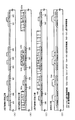
図4(A)は電流制御用TFTのトランジスタ特性を示すグラフであり、401はId−Vg特性(又はId−Vg曲線)と呼ばれている。ここでIdはドレイン電流であり、Vgはゲート電圧である。このグラフにより任意のゲート電圧に対して流れる電流量を知ることができる。
【0007】
通常、EL素子を駆動するにあたって、上記Id−Vg特性の点線402で示した領域を用いる。402で囲んだ領域の拡大図を図4(B)に示す。
【0008】
図4(B)において、斜線で示す領域はサブスレッショルド領域と呼ばれている。実際にはしきい値電圧(Vth)近傍又はそれ以下のゲート電圧である領域を指し、この領域ではゲート電圧の変化に対して指数関数的にドレイン電流が変化する。この領域を使ってゲート電圧による電流制御を行う。
【0009】
図3におけるスイッチング用TFT301が開いて画素内に入力されたデータ信号は、まずコンデンサ304に蓄積され、その信号がそのまま電流制御用TFT302のゲート電圧となる。このとき、図4(A)に示したId−Vg特性に従ってゲート電圧に対してドレイン電流が1対1で決まる。即ち、データ信号に対応して所定の電流がEL素子303を流れ、その電流量に対応した発光量で前記EL素子303が発光する。
【0010】
以上のように、入力される信号によってEL素子の発光量が制御され、その発光量の制御によって階調表示がなされる。この方式はいわゆるアナログ階調と呼ばれる方式であり、信号の振幅の変化で階調表示が行われる。
【0011】
しかしながら、上記アナログ階調方式はTFTの特性バラツキに非常に弱いという欠点がある。例えばスイッチング用TFTのId−Vg特性が同じ階調を表示する隣接画素のスイッチング用TFTと異なる場合(全体的にプラス又はマイナス側へシフトした場合)を想定する。
【0012】
その場合、各スイッチング用TFTのドレイン電流はバラツキの程度にもよるが異なるものとなり、各画素の電流制御用TFTには異なるゲート電圧がかかることになる。即ち、各EL素子に対して異なる電流が流れ、結果として異なる発光量となり、同じ階調表示を行えなくなる。
【0013】
また、仮に各画素の電流制御用TFTに等しいゲート電圧がかかったとしても、電流制御用TFTのId−Vg特性にバラツキがあれば、同じドレイン電流を出力することはできない。さらに、図4(A)からも明らかなようにゲート電圧の変化に対して指数関数的にドレイン電流が変化するような領域を使っているため、Id−Vg特性が僅かでもずれれば、等しいゲート電圧がかかっても出力される電流量は大きく異なるといった事態が生じうる。こうなってしまうとEL素子の発光量が隣接画素で大きく異なってしまう。
【0014】
実際には、スイッチング用TFTと電流制御用TFTとの、両者のバラツキの相乗効果となるので条件的にはさらに厳しい。このように、アナログ階調方式はTFTの特性バラツキに対して極めて敏感であり、その点が従来のアクティブマトリクス型EL表示装置の多色カラー化における障害となっている。
【0015】
【発明が解決しようとする課題】
本発明は上記問題点を鑑みてなされたものであり、鮮明な多階調カラー表示の可能なアクティブマトリクス型EL表示装置を提供することを課題とする。そして、そのようなアクティブマトリクス型EL表示装置を表示部として具備する高性能な電気器具を提供することを課題とする。
【0016】
【課題を解決するための手段】
本出願人は、TFT特性のバラツキの影響を受けにくい画素構造とするためには、電流制御によってEL素子の発光量を制御する従来のアナログ駆動の階調方式よりも、電流制御用TFTを単に電流供給用のスイッチング素子として用いたデジタル駆動の階調方式の方が良いと考えた。
【0017】
そこで、アクティブマトリクス型EL表示装置においてデジタル駆動で、時間分割方式の階調表示(以下、時分割階調という)を行うことを考えた。
【0018】
さらに、ソース駆動回路にビデオ信号を入力する際、ビデオ線を分割して、一度に複数のデータを入力することで、パネル表示の高速化を実現した。なお、ここでいうビデオ信号は、本明細書中のソース駆動回路に入力されるデータ信号のことである。
【0019】
図5に時分割階調表示を行う際の書込期間と表示期間の駆動タイミング全体を示す。ここでは6ビットデジタル駆動方式により64階調表示を行う場合について説明する。なお、書込期間とは、1フレームを構成する全ての画素に信号が書き込まれるのに要する時間であり、表示期間とは、書込に対して画素表示が行われる期間を示している。
【0020】
書込期間ではEL駆動電源を切り(全画素消灯)、画素内のEL素子に電圧がかからない状態にする。また、表示期間ではEL駆動電源を入れ、画素内のEL素子に電圧がかかる状態にしてある。このとき画素が点灯するデータ信号が入力されると画素は点灯する。
【0021】
表示領域の画像が完全に表示される期間を1フレームと呼ぶ。通常のELディスプレイでは発振周波数は60Hzであり、図5(a)に示すように1秒間には、60フレーム存在することになる。例えば4番目の1フレームにおいて6ビットデジタル階調(64階調)表示を行う場合、1フレームを16分割して書込期間と表示期間の比率を6:10に決めると図5(b)に示すように書込期間(≒6.24msec)に6回の書込ができる。なお、この6回の書込を書き込む順に書込1から書込6とする。また、書込期間(書込1から書込6)に対応する表示期間をそれぞれ表示1から表示6とする。
【0022】
また、表示期間については、表示1:表示2:表示3:表示4:表示5:表示6=1:1/2:1/4:1/8:1/16:1/32となるように設定する。
【0023】
図5(c)は、1フレーム中で6回の書込(書込1から書込6)を行う際、各表示期間が、それぞれの書込に対して上記の比になる様子を示したものである。ここで、図5(c)の下部に示されている数値は、書込期間と表示期間の長さの関係を示すものである。
【0024】
具体的には、書込1における表示期間(表示1)は、書込期間を63としたときに320に値することを示している。さらに、各書込期間が63であるのに対して、表示2は表示期間が160、表示3は表示期間が80、表示4は表示期間が40、表示5は表示期間が20、表示6は表示期間が10にそれぞれ値することを示している。
【0025】
1書込期間(書込)と1表示期間(表示)をあわせて1フィールドという。つまり、図5(c)には、書込期間が全て一定で表示期間の異なる6つのフィールドが存在することになる。ここで1フレームを完成させるために、はじめに表示される1つ目のフィールドをフィールド1(F1)と呼び、以下表示される順に2つ目のフィールドから6つ目のフィールドまでをフィールド2(F2)〜フィールド6(F6)と呼ぶ。
但し、フィールド1からフィールド6を出現させる順序はどのようにしても良い。この表示期間の組み合わせで64階調のうち所望の階調表示を行うことができる。
【0026】
また、実際のタイミングは、図5(d)に示すように表示期間の異なる6つのフィールドを分散させた組み合わせにする。
【0027】
図5(d)においては、表示1の期間、所定の画素を点灯させるとすると次に、書込5に入り、全画素にデータ信号を入力したら表示5に入る。つぎに書込4で全画素にデータ信号を入力したら表示4に入る。このようにして、書込2、書込3、書込6においても同様にそれぞれのフィールドで表示所定の画素を点灯させる。
【0028】
図5(e)は、図5(d)に示された6つのフィールドのフィールド5においてゲート回路から入力されるデータ信号によってあるゲート線が選択されるというデータが書き込まれる期間(書込5)と、選択されたゲート線にソース線からの信号が入力されて画素が表示される表示期間(表示5)を示したものである。
【0029】
図5は、VGA(640×480)のパネル表示をもとにしているため、ゲート配線は480本であり、さらに何本かのダミーを含むゲート線全てを選択する期間が、図5(e)の書込期間である。
【0030】
書込期間においてソース線から入力される信号をドットデータという。1ゲート選択期間にソース駆動回路から入力されるドットデータは、図5(f)に示す期間でサンプリングされる。これは、図5(e)に示す書込期間に選択されるゲートのデータが書き込まれると同時にソース線から入力された信号が書き込まれていることを示している。なお、データが一度にサンプリングされる期間は、40nsec.である。
【0031】
なお、ソース駆動回路から入力されるドットデータは、図5(f)に示すように16個ずつ40nsec.ごとに同時に入力される。
【0032】
さらに、1ゲート選択期間に選択されるドットデータは、全てのデータサンプリングがなされるまで、図6に示すソース駆動回路内のラッチ1(6001)にそれぞれ保持され、全てのサンプリングが終了した後にラッチ線6003からラッチデータが入力されて、全てのデータが一斉にラッチ2(6002)に移動する。なお、シフトレジスタ6004は、クロック線6005からのクロックパルスによりビデオ線6006から入力されるビデオ信号を選択している。
【0033】
図5(f)中にサンプリング期間の他に設けられているラインデータラッチ期間とは、ラッチ1(6001)からラッチ2(6002)にデータを移動させる際にラッチ信号が入力され、データが移動する期間のことをいう。
【0034】
本発明におけるアクティブマトリクス型EL表示装置の画素構造を図7に示す。図7において、701はスイッチング素子として機能するTFT(以下、スイッチング用TFTまたは、画素スイッチTFTという)、702はEL素子703に供給する電流を制御するための素子(電流制御素子)として機能するTFT(以下、電流制御用TFTまたはEL駆動TFTという)、704はコンデンサ(保持容量または、補助容量という)である。スイッチング用TFT701はゲート線705及びソース線(データ線)706に接続されている。また、電流制御用TFT702のドレインはEL素子703に、ソースは電流供給線(または、EL駆動電源線という)707に接続されている。
【0035】
ゲート線705が選択されるとスイッチング用TFT701のゲートが開き、ソース線706のデータ信号がコンデンサ704に蓄積され、電流制御用TFT702のゲートが開く。そして、スイッチング用TFT701のゲートが閉じた後、コンデンサ704に蓄積された電荷によって電流制御用TFT702のゲートは開いたままとなり、その間、EL素子703が発光する。このEL素子703の発光量は流れる電流量で変化する。
【0036】
つまり、デジタル駆動の階調表示において、ソース線706から入力されるデータ信号によって電流制御用TFT702のゲートが開または閉になり、EL駆動電源が入ると電流が流れ、EL素子が発光するのである。
【0037】
画素の電流制御用TFTの機能は、表示期間に当該画素を点灯(表示)させるか消灯(非表示)させるかを制御することである。表示期間と書込期間の切り替えは、右のパネル外の電源がFPC端子を通して行う。
【0038】
また、パネル外に取り付けられた電源(図7の72の709)は、書込期間と表示期間を切り替えるためのスイッチ機能を果たしている。書込期間では、この電源を切った状態(電圧を加えない状態)で、各画素にデータ信号を入力していく。
【0039】
そして、全ての画素にデータが入力されて書込期間が終了したら、電源(図7の72の709)を入れ、一斉に表示を行う。この期間が表示期間となる。EL素子が発光し画素を点灯させる期間は6つのフィールドのうち表示1〜表示6までのいずれかの期間である。
【0040】
6つのフィールドが出現したら1フレームを終えたことになる。このとき、表示期間の積算によってその画素の階調が制御される。例えば、表示1と表示2を選択した場合には全灯を100%としたうちの76%の輝度が表現でき、表示3と表示5を選択した場合には16%の輝度が表現できる。
【0041】
なお、以上は64階調の場合について説明したが、他の階調表示を行うことも可能である。
【0042】
仮にNビット(Nは2以上の整数)の階調(2n階調)の表示を行う場合には、図8に示すように、まず1フレームをNビットの階調に対応させてN枚のフィールド(F1、F2、F3…F(n-1)、F(n)と表す)に分割する。階調が多くなるにつれて1フレームの分割数も増え、駆動回路を高い周波数で駆動しなければならない。
【0043】
さらに、これらN枚の各フィールドは書込期間(Ta)及び表示期間(Ts)に分離される。
【0044】
そして、N枚の各フィールドの表示期間(但し、F1、F2、F3…F(n-1)、F(n)に対応する表示期間を各々Ts1、Ts2、Ts3…Ts(n-1)、Ts(n)と表す)をTs1:Ts2:Ts3:…:Ts(n-1):Ts(n)=20:2-1:2-2:…:2-(n-2):2-(n-1)となるように処理する。
【0045】
この状態で、任意の1フィールドでは順次画素が選択され(厳密には各画素のスイッチング用TFTが選択され)、電流制御用TFTのゲート電極に所定のゲート電圧(データ信号に対応する)が加わる。このとき、電流制御用TFTが導通状態になるようなデータ信号が入力された画素のEL素子は、書込期間終了後、電源が入力されるとそのフィールドに割り当てられた表示期間だけ画素が点灯する。
【0046】
この動作をN枚のフィールド全てにおいて繰り返し、その表示期間の積算によって1フレームにおける各画素の階調が制御される。従って、任意の1画素に注目すると、その画素が各フィールドでどれだけの期間点灯したか(どれだけの表示期間を経由したか)によって、その1画素の階調が制御される。
【0047】
以上のように、アクティブマトリクス型EL表示装置にデジタル駆動の時分割階調方式を用いる点が本発明の最大の特徴である。この時分割階調駆動を用いることでアナログ駆動の階調表示において問題であったTFT特性の影響を受けずに階調表示を行うことが可能となる。
【0048】
【発明の実施の形態】
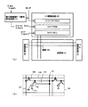
図1は、本実施例のアクティブマトリクス型EL表示装置の概略ブロック図である。図1のアクティブマトリクス型EL表示装置は、基板上に形成されたTFTによって画素部101、画素部の周辺に配置されたソース駆動回路102、ゲート駆動回路103が形成される。また、113は時分割階調データ信号発生回路(SPC;Serial-to-Parallel Conversion Circuit)である。
【0049】
ソース駆動回路102は、シフトレジスタ102a、ラッチ1(102b)、ラッチ2(102c)を有している。その他、バッファ(図示せず)を有している。
【0050】
なお、本実施例のアクティブマトリクス型EL表示装置においては、ソース駆動回路を1つだけ設けているが、画素部の上下を挟むように2つのソース駆動回路を設けても良い。
【0051】
また、103はゲート駆動回路であり、シフトレジスタ、バッファ等(いずれも図示せず)を有している。
【0052】
画素部101は、640×480(横×縦)の画素を有している。各画素にはスイッチング用TFTおよび電流制御用TFTが配置されている。スイッチング用TFT105はゲート線106及びソース線(データ線)107に接続されている。また、電流制御用TFT108のドレインはEL素子109に、ソースは電流供給線110に接続されている。
ゲート線106が選択されるとスイッチング用TFT105のゲートが開き、ソース線107のデータ信号がコンデンサ112に蓄積され、電流制御用TFT108のゲートが開く。つまり、ソース線107から入力されるデータ信号により電流制御用TFT108に電流が流れ、EL素子が発光する。
【0053】
ここで、本実施例のアクティブマトリクス型EL表示装置の動作および信号の流れを説明する。
【0054】
まず、ソース駆動回路102の動作を説明する。ソース駆動回路102は、基本的にシフトレジスタ102a、ラッチ1(102b)、ラッチ2(102c)を含む。シフトレジスタ102aにクロック信号(CK)およびスタートパルス(SP)が入力される。シフトレジスタ102aは、これらのクロック信号(CK)およびスタートパルス(SP)に基づきタイミング信号を順に発生させ、バッファ(図示せず)を通して後段の回路へタイミング信号を順次供給する。
【0055】
シフトレジスタ102aからのタイミング信号は、バッファ等によって緩衝増幅される。タイミング信号が供給されるソース線には、多くの回路あるいは素子が接続されているために負荷容量(寄生容量)が大きい。この負荷容量が大きいために生ずるタイミング信号の立ち上がりまたは立ち下がりの”鈍り”を防ぐために、このバッファが設けられる。
【0056】
バッファによって緩衝増幅されたタイミング信号(デジタルデータ信号(Digital Data Signals))は、ラッチ1(102b)に供給される。ラッチ1(102b)は、6ビットデジタル信号(6bit digital signal)を処理するラッチを有する。ラッチ1(102b)は、前記タイミング信号が入力されると、時分割階調データ信号発生回路113から供給される6ビットデジタルデータ信号を順次取り込み、保持する。
【0057】
ラッチ1(102b)の全てのステージにデジタルデータ信号の書込が一通り終了するまでの時間を書込期間という。すなわち、ラッチ1(102b)の中で一番左側のステージのラッチにデジタルデータ信号が書き込まれる時点から、一番右側のステージのラッチにデジタルデータ信号の書込が終了する時点までが書込期間である。また、上記書込期間をライン期間と呼ぶこともある。
【0058】
書込期間終了後、シフトレジスタ102aの動作タイミングに合わせて、ラッチ2(102c)にラッチシグナル(Latch Signal)が供給される。この瞬間、ラッチ1(102b)に書き込まれ保持されているデジタルデータ信号は、ラッチ2(102c)に一斉に送出され、ラッチ2(102c)に保持される。
【0059】
デジタル信号をラッチ2(102c)に送出し終えたラッチ1(102b)には、シフトレジスタ102aからのタイミング信号に基づき、再び時分割階調データ信号発生回路113から供給されるデジタル信号の書込が順次行われる。
【0060】
また、ラッチ2(102c)にはラッチ信号(Latch Signals)が入力される。
【0061】
ゲート駆動回路103においては、シフトレジスタ(図示せず)からのタイミング信号がバッファ(図示せず)に供給され、対応するゲート線(走査線)に供給される。
【0062】
113は時分割階調データ信号発生回路(SPC;Serial-to-Parallel Conversion Circuit)である。時分割階調データ信号発生回路113は、外部から入力されるデジタル信号の周波数を1/mに落とすための回路である。外部から入力されるデジタル信号を分割することにより、駆動回路の動作に必要な信号の周波数も1/mに落とすことができる。
【0063】
本発明では画素部に入力されるデータ信号がデジタル信号であり、また液晶表示装置と異なり電圧階調表示ではないので、「0」または「1」の情報を有するデジタルデータ信号がそのまま画素部へと入力される。
【0064】
画素部101にはマトリクス状に複数の画素104が配列される。画素104の拡大図を図1(B)に示す。図1(B)において、105はスイッチング用TFTであり、ゲート信号を入力するゲート線106とビデオ信号を入力するソース配線107に接続されている。
【0065】
また、108は電流制御用TFTであり、そのゲートはスイッチング用TFT105のドレインに接続される。そして、電流制御用TFT108のドレインはEL素子109に接続され、ソースは電流供給線110に接続される。EL素子109は電流制御用TFT108に接続された陽極(画素電極)と、EL層を挟んで陽極に対向して設けられた陰極(対向電極)とからなり、陰極は所定の電源111に接続されている。
【0066】
なお、スイッチング用TFT105は、nチャネル型TFTでもpチャネル型TFTでもよい。
【0067】
また、電流制御用TFT108においては、電流制御用TFT108が、nチャネル型TFTである場合には、電流制御用TFT108のドレイン部はEL素子109の陰極に接続され、電流制御用TFT108が、pチャネル型TFTである場合には、電流制御用TFT108のドレイン部はEL素子109の陽極に接続される構造をとる。
【0068】
また、スイッチング用TFT105が非選択状態(オフ状態)にある時、電流制御用TFT108のゲート電圧を保持するためにコンデンサ112が設けられる。このコンデンサ112はスイッチング用TFT105のドレインと電流供給線110とに接続されている。
【0069】
以上のような画素部に入力されるデジタルデータ信号は、時分割階調データ信号発生回路113にて形成される。この回路ではデジタル信号からなるビデオ信号(画像情報を含む信号)を、時分割階調を行うためのデジタルデータ信号に変換すると共に、時分割階調表示を行うために必要なタイミングパルス等を発生させる回路である。
【0070】
典型的には、時分割階調データ信号発生回路113には、1フレームをNビット(Nは2以上の整数)の階調に対応した複数のフィールドに分割する手段と、それら複数のフィールドにおいて書込期間及び表示期間を選択する手段と、その表示期間をTs1:Ts2:Ts3:…:Ts(n-1):Ts(n)=20:2-1:2-2:…:2-(n-2):2-(n-1)となるように設定する手段とが含まれる。
【0071】
時分割階調データ信号発生回路113は、本発明のEL表示装置の外部に設けても良いし、一体形成しても良い。EL表示装置の外部に設けられる場合、そこで形成されたデジタルデータ信号が本発明のEL表示装置に入力される構成となる。
【0072】
次に、本発明のアクティブマトリクス型EL表示装置について、断面構造の概略を図2に示す。
【0073】
図2において、11は基板、12は下地となる絶縁膜(以下、下地膜という)である。基板11としては透光性基板、代表的にはガラス基板、石英基板、ガラスセラミックス基板、又は結晶化ガラス基板を用いることができる。但し、作製プロセス中の最高処理温度に耐えるものでなくてはならない。
【0074】
また、下地膜12は特に可動イオンを含む基板や導電性を有する基板を用いる場合に有効であるが、石英基板には設けなくても構わない。下地膜12としては、珪素(シリコン)を含む絶縁膜を用いれば良い。なお、本明細書において「珪素を含む絶縁膜」とは、具体的には酸化珪素膜、窒化珪素膜若しくは窒化酸化珪素膜(SiOxNy:x、yは任意の整数、で示される)など珪素に対して酸素若しくは窒素を所定の割合で含ませた絶縁膜を指す。
【0075】
201はスイッチング用TFTであり、nチャネル型TFTで形成されているが、スイッチング用TFTは、pチャネル型としてもよい。また、202は電流制御用TFTであり、図2は、電流制御用TFT202がpチャネル型TFTで形成された場合を示している。つまり、この場合は、電流制御用TFTのドレイン電極は、EL素子の陽極に接続される。しかし、電流制御用TFTがnチャネル型TFTで形成された場合には、電流制御用TFTはEL素子の陰極に接続される。
【0076】
nチャネル型TFTの電界効果移動度はpチャネル型TFTの電界効果移動度よりも大きいため、動作速度が早く大電流を流しやすい。また、同じ電流量を流すにもTFTサイズはnチャネル型TFTの方が小さくできる。
【0077】
ただし、本発明において、スイッチング用TFTと電流制御用TFTをnチャネル型TFTに限定する必要はなく、両方又はどちらか片方にpチャネル型TFTを用いることも可能である。
【0078】
スイッチング用TFT201は、ソース領域13、ドレイン領域14、LDD領域15a〜15d、分離領域16及びチャネル形成領域17a、17bを含む活性層、ゲート絶縁膜18、ゲート電極19a、19b、第1層間絶縁膜20、ソース配線21並びにドレイン線22を有して形成される。なお、ゲート絶縁膜18又は第1層間絶縁膜20は基板上の全TFTに共通であっても良いし、回路又は素子に応じて異ならせても良い。
【0079】
また、図2に示すスイッチング用TFT201はゲート電極19a、19bが電気的に接続されており、いわゆるダブルゲート構造となっている。勿論、ダブルゲート構造だけでなく、トリプルゲート構造などいわゆるマルチゲート構造(直列に接続された二つ以上のチャネル形成領域を有する活性層を含む構造)であっても良い。
【0080】
マルチゲート構造はオフ電流を低減する上で極めて有効であり、スイッチング用TFTのオフ電流を十分に低くすれば、それだけ図1(B)に示すコンデンサ112に必要な容量を小さくすることができる。即ち、コンデンサ112の専有面積を小さくすることができるので、マルチゲート構造とすることはEL素子109の有効発光面積を広げる上でも有効である。
【0081】
さらに、スイッチング用TFT201においては、LDD領域15a〜15dは、ゲート絶縁膜18を介してゲート電極17a、17bと重ならないように設ける。このような構造はオフ電流を低減する上で非常に効果的である。また、LDD領域15a〜15dの長さ(幅)は0.5〜3.5μm、代表的には2.0〜2.5μmとすれば良い。
【0082】
なお、チャネル形成領域とLDD領域との間にオフセット領域(チャネル形成領域と同一組成の半導体層からなり、ゲート電圧が印加されない領域)を設けることはオフ電流を下げる上でさらに好ましい。また、二つ以上のゲート電極を有するマルチゲート構造の場合、チャネル形成領域の間に設けられた分離領域16(ソース領域又はドレイン領域と同一の濃度で同一の不純物元素が添加された領域)がオフ電流の低減に効果的である。
【0083】
次に、電流制御用TFT202は、ソース領域26、ドレイン領域27、チャネル形成領域29、ゲート絶縁膜18、ゲート電極30、第1層間絶縁膜20、ソース配線31並びにドレイン線32を有して形成される。なお、ゲート電極30はシングルゲート構造となっているが、マルチゲート構造であっても良い。
【0084】
図1(B)に示すように、スイッチング用TFTのドレインは電流制御用TFTのゲートに接続されている。具体的には電流制御用TFT202のゲート電極30はスイッチング用TFT201のドレイン領域14とドレイン配線(接続配線とも言える)22を介して電気的に接続されている。また、ソース配線31は図1(B)の電流供給線110に接続される。
【0085】
また、流しうる電流量を多くするという観点から見れば、電流制御用TFT202の活性層(特にチャネル形成領域)の膜厚を厚くする(好ましくは50〜100nm、さらに好ましくは60〜80nm)ことも有効である。逆に、スイッチング用TFT201の場合はオフ電流を小さくするという観点から見れば、活性層(特にチャネル形成領域)の膜厚を薄くする(好ましくは20〜50nm、さらに好ましくは25〜40nm)ことも有効である。
【0086】
以上は画素内に設けられたTFTの構造について説明したが、このとき同時に駆動回路も形成される。図2には駆動回路を形成する基本単位となるCMOS回路が図示されている。
【0087】
図2においては極力動作速度を落とさないようにしつつホットキャリア注入を低減させる構造を有するTFTをCMOS回路のnチャネル型TFT204として用いる。なお、ここでいう駆動回路としては、図1に示したソース駆動回路102、ゲート信号駆動回路103を指す。勿論、他の論理回路(レベルシフタ、A/Dコンバータ、信号分割回路等)を形成することも可能である。
【0088】
nチャネル型204の活性層は、ソース領域35、ドレイン領域36、LDD領域37及びチャネル形成領域38を含み、LDD領域37はゲート絶縁膜18を介してゲート電極39と重なっている。本明細書中では、このLDD領域37をLov領域ともいう。
【0089】
ドレイン領域側のみにLDD領域を形成しているのは、動作速度を落とさないための配慮である。また、このnチャネル型TFT204はオフ電流値をあまり気にする必要はなく、それよりも動作速度を重視した方が良い。従って、LDD領域37は完全にゲート電極に重ねてしまい、極力抵抗成分を少なくすることが望ましい。即ち、いわゆるオフセットはなくした方がよい。
【0090】
また、CMOS回路のpチャネル型TFT205は、ホットキャリア注入による劣化が殆ど気にならないので、特にLDD領域を設けなくても良い。従って活性層はソース領域40、ドレイン領域41及びチャネル形成領域42を含み、その上にはゲート絶縁膜18とゲート電極43が設けられる。勿論、nチャネル型TFT204と同様にLDD領域を設け、ホットキャリア対策を講じることも可能である。
【0091】
また、nチャネル型TFT204及びpチャネル型TFT205はそれぞれ第1層間絶縁膜20に覆われ、ソース配線44、45が形成される。また、ドレイン配線46によって両者は電気的に接続される。
【0092】
次に、47は第1パッシベーション膜であり、膜厚は10nm〜1μm(好ましくは200〜500nm)とすれば良い。材料としては、珪素を含む絶縁膜(特に窒化酸化珪素膜又は窒化珪素膜が好ましい)を用いることができる。このパッシベーション膜47は形成されたTFTをアルカリ金属や水分から保護する役割をもつ。最終的にTFTの上方に設けられるEL層にはナトリウム等のアルカリ金属が含まれている。即ち、第1パッシベーション膜47はこれらのアルカリ金属(可動イオン)をTFT側に侵入させない保護層としても働く。しかし、このパッシベーション膜は必ずしも設けなければならないものではなく、必要に応じて設けるようにすればよい。
【0093】
また、48は第2層間絶縁膜であり、TFTによってできる段差の平坦化を行う平坦化膜としての機能を有する。第2層間絶縁膜48としては、有機樹脂膜が好ましく、ポリイミド、ポリアミド、アクリル、BCB(ベンゾシクロブテン)等を用いると良い。これらの有機樹脂膜は良好な平坦面を形成しやすく、比誘電率が低いという利点を有する。EL層は凹凸に非常に敏感であるため、TFTによる段差は第2層間絶縁膜で殆ど吸収してしまうことが望ましい。また、ゲート配線やデータ配線とEL素子の陰極との間に形成される寄生容量を低減する上で、比誘電率の低い材料を厚く設けておくことが望ましい。従って、膜厚は0.5〜5μm(好ましくは1.5〜2.5μm)が好ましい。
【0094】
また、49は透明導電膜からなる画素電極(EL素子の陽極)であり、第2層間絶縁膜48及び第1パッシベーション膜47にコンタクトホール(開孔)を開けた後、形成された開孔部において電流制御用TFT202のドレイン配線32に接続されるように形成される。なお、図2のように画素電極49とドレイン領域27とが直接接続されないようにしておくと、EL層のアルカリ金属が画素電極を経由して活性層へ侵入することを防ぐことができる。
【0095】
画素電極49の上には酸化珪素膜、窒化酸化珪素膜または有機樹脂膜からなる第3層間絶縁膜50が0.3〜1μmの厚さに設けられる。この第3層間絶縁膜50は画素電極49の上にエッチングにより開口部が設けられ、その開口部の縁はテーパー形状となるようにエッチングする。テーパーの角度は10〜60°(好ましくは30〜50°)とすると良い。
【0096】
第3層間絶縁膜50の上にはEL層51が設けられる。EL層51は単層又は積層構造で用いられるが、積層構造で用いた方が発光効率は良い。一般的には画素電極上に正孔注入層/正孔輸送層/発光層/電子輸送層の順に形成されるが、正孔輸送層/発光層/電子輸送層、または正孔注入層/正孔輸送層/発光層/電子輸送層/電子注入層のような構造でも良い。本発明では公知のいずれの構造を用いても良いし、EL層に対して蛍光性色素等をドーピングしても良い。
【0097】
有機EL材料としては、公知の材料を用いることができるが、例えば、以下の米国特許又は公開公報に開示された材料を用いることができる。米国特許第4,356,429号、 米国特許第4,539,507号、 米国特許第4,720,432号、 米国特許第4,769,292号、 米国特許第4,885,211号、 米国特許第4,950,950号、 米国特許第5,059,861号、 米国特許第5,047,687号、 米国特許第5,073,446号、 米国特許第5,059,862号、 米国特許第5,061,617号、 米国特許第5,151,629号、 米国特許第5,294,869号、 米国特許第5,294,870号、特開平10−189525号公報、特開平8−241048号公報、特開平8−78159号公報。
【0098】
なお、EL表示装置には大きく分けて四つのカラー化表示方式があり、R(赤)G(緑)B(青)に対応した三種類のEL素子を形成する方式、白色発光のEL素子とカラーフィルターを組み合わせた方式、青色又は青緑発光のEL素子と蛍光体(蛍光性の色変換層:CCM)とを組み合わせた方式、陰極(対向電極)に透明電極を使用してRGBに対応したEL素子を重ねる方式、がある。
【0099】
図2の構造はRGBに対応した三種類のEL素子を形成する方式を用いた場合の例である。なお、図2には一つの画素しか図示していないが、同一構造の画素が赤、緑又は青のそれぞれの色に対応して形成され、これによりカラー表示を行うことができる。
【0100】
本発明は発光方式に関わらず実施することが可能であり、上記四つの全ての方式を本発明に用いることができる。しかし、蛍光体はELに比べて応答速度が遅く残光が問題となりうるので、蛍光体を用いない方式が望ましい。また、発光輝度を落とす要因となるカラーフィルターもなるべく使わない方が望ましいと言える。
【0101】
EL層51の上にはEL素子の陰極52が設けられる。陰極52としては、仕事関数の小さいマグネシウム(Mg)、リチウム(Li)若しくはカルシウム(Ca)を含む材料を用いる。好ましくはMgAg(MgとAgをMg:Ag=10:1で混合した材料)からなる電極を用いれば良い。他にもMgAgAl電極、LiAl電極、また、LiFAl電極が挙げられる。
【0102】
陰極52はEL層51を形成した後、大気解放しないで連続的に形成することが望ましい。陰極52とEL層51との界面状態はEL素子の発光効率に大きく影響するからである。なお、本明細書中では、画素電極(陽極)、EL層及び陰極で形成される発光素子をEL素子と呼ぶ。
【0103】
EL層51と陰極52からなる積層体は、各画素で個別に形成する必要があるが、EL層51は水分に極めて弱いため、通常のフォトリソグラフィ技術を用いることができない。従って、メタルマスク等の物理的なマスク材を用い、真空蒸着法、スパッタ法、プラズマCVD法等の気相法で選択的に形成することが好ましい。
【0104】
なお、EL層を選択的に形成する方法として、インクジェット法やスクリーン印刷法等を用いることも可能であるが、これらは現状では陰極の連続形成ができないので、上述の方法の方が好ましいと言える。
【0105】
また、53は保護電極であり、陰極52を外部の水分等から保護すると同時に、各画素の陰極52を接続するための電極である。保護電極53としては、アルミニウム(Al)、銅(Cu)若しくは銀(Ag)を含む低抵抗な材料を用いることが好ましい。この保護電極53にはEL層の発熱を緩和する放熱効果も期待できる。また、上記EL層51、陰極52を形成した後、大気解放しないで連続的に保護電極53まで形成することも有効である。
【0106】
また、54は第2パッシベーション膜であり、膜厚は10nm〜1μm(好ましくは200〜500nm)とすれば良い。第2パッシベーション膜54を設ける目的は、EL層51を水分から保護する目的が主であるが、放熱効果をもたせることも有効である。但し、上述のようにEL層は熱に弱いのからなるべく低温(好ましくは室温から120℃までの温度範囲)で成膜するのが望ましい。従って、プラズマCVD法、スパッタ法、真空蒸着法、イオンプレーティング法又は溶液塗布法(スピンコーティング法)が望ましい成膜方法と言える。しかし、この第2パッシベーション膜54は、必ずしも設けなければならないものではなく、必要に応じて設けるようにすればよい。
【0107】
本発明の主旨は、アクティブマトリクス型EL表示装置において、アナログ駆動の階調表示をデジタル駆動の時分割階調表示にすることで、これまでアナログ駆動の階調において問題となっていたTFTのバラつきの問題を改善したというものである。従って、図2のEL表示装置の構造に限定されるものではなく、図2の構造は本発明を実施する上での好ましい形態の一つに過ぎない。
【0108】
上記ポリシリコン膜を用いたTFTは、高い動作速度を示すが故にホットキャリア注入などの劣化も起こりやすい。そのため、図2のように、画素内において機能に応じて構造の異なるTFT(オフ電流の十分に低いスイッチング用TFTと、ホットキャリア注入に強い電流制御用TFT)を形成することは、高い信頼性を有し、且つ、良好な画像表示が可能な(動作性能の高い)EL表示装置を作製する上で非常に有効である。
【0109】
〔実施例1〕
本発明の実施例について図9〜図16および表1〜4を用いて説明する。
ここでは、本発明を実施する上で用いる画素部とその周辺に設けられる駆動回路構成およびその仕様(サイズおよび電圧値等)、さらに入力される信号について説明する。
図9は、上面(陰極成膜側)からみたパネル全体の平面図である。ここで、表示は下面に向かってなされる。図9において901は画素部であり、902はソース駆動回路、903はゲート駆動回路、904はフレキシブルプリントサーキット(以下FPC)入力部である。なお、本実施例において用いたFPC入力部904は、300μmピッチで50本の端子を有する。
【0110】
本実施例において図9のFPC入力部904は、図10に示すFPC入力部の保護回路を有する。ただし、ビデオ信号入力端子(図9中のFPC入力部904の上部に付けられている番号(1〜50)のうちの5〜20、27〜42)には、抵抗(R1)はない。
なお、FPC入力端子部の保護回路を有するのは、図9中のFPC入力部904の上部に付けられている番号(1〜50)のうちの1、2、21、22、43、44、49、50を除く部分である。
【0111】
さらに、本実施例において用いたFPC入力端子の仕様を表1に示す。なお、表1に示されている「端子No.」は、図9中のFPC入力部904の上部に付けられている番号(1〜50)と対応している。
【0112】
【表1】

次に、図9のゲート駆動回路903の詳細な回路図を図11に示す。ゲート駆動回路における正電源電圧は10Vであり、負電源電圧は0V、ゲート駆動回路に入力される動作クロックの周波数は、232kHzである。また、このゲート駆動回路は、走査方向の切り替え機能を有する。
【0114】
図11における記号g_chsw_aは、走査方向切り替えスイッチ、g_sftr_b、g_sftr_c、g_sftr_dは、シフトレジスタの一部であり、g_nand_eは、NAND回路、g_buff_fは、バッファを示す。
【0115】
本実施例では、図11中の破線で囲まれている部分、つまりg_chsw_a、g_sftr_b、g_sftr_c、g_sftr_dから構成される部分をシフトレジスタ(11001)という。
【0116】
本実施例のゲート駆動回路を構成するシフトレジスタ、NAND回路、バッファに含まれるTFTのサイズを表2に示す。
シフトレジスタ、NAND回路、バッファには、p型のTFTおよびn型のTFTが用いられているので、それぞれについて示した。表2中のサイズは、図10に示されている記号にそれぞれ対応している。また、表中においてL[μm]は、TFTのチャネル長を示し、W[μm]は、TFTのチャネル幅を示す。なお、n型TFTのチャネル長には、Lov領域が含まれている。
【0117】
【表2】
次に、図9のソース駆動回路902の詳細な回路図を図12に示す。ソース駆動回路における正電源電圧は9Vであり、負電源電圧は0Vで、ソース駆動回路に入力される動作クロックの周波数は、12.5MHzであり、走査方向の切り替え機能を有する。
【0119】
図12におけるs_chsw_aは、走査方向切り替えスイッチ、g_sftr_b、g_sftr_c、g_sftr_dは、シフトレジスタの一部、s_nand_eは、NAND回路、s_buf_f、s_buf_g、s_buf_h、s_buf_iは、いずれもバッファである。また、s_lat1_j、s_lat1_k、s_lat1_m、s_lat1_nは、いずれも1段目のラッチ(以下ラッチ1という)を示し、s_lat2_p、s_lat2_r、s_lat2_sは、いずれも2段目のラッチ(以下ラッチ2という)を示す。
【0120】
本実施例では、図12中の破線で囲まれている部分、つまりs_chsw_a、s_sftr_b、s_sftr_c、s_sftr_dから構成される部分をシフトレジスタ(12001)という。
【0121】
次に本実施例のソース駆動回路を構成するシフトレジスタ、NAND回路、バッファに含まれるTFTのサイズを表3に示す。シフトレジスタ、NAND回路、バッファには、p型のTFTおよびn型のTFTが用いられているので、それぞれについて示した。表3中のサイズは、図12に示されている記号にそれぞれ対応している。また、表中においてL[μm]は、TFTのチャネル長を示し、W[μm]は、TFTのチャネル幅を示す。なお、n型TFTのチャネル長には、Lov領域が含まれている。
【0122】
【表3】
ここで、ゲート駆動回路から入力された信号のタイミングチャートを図13、図14に示す。図13はゲート線の選択が下方向走査の場合であり、図14は、上方向走査の場合である。なお、これは、1フィールドを単位として示している。
【0124】
図13、図14には、FPCから入力される信号とゲート駆動回路から入力される信号を示す。FPC入力信号において、EL_CATHは、ELを駆動させる直流電源、G_UPは、ゲート駆動回路の走査方向を切り替える信号、G_CKは、ゲート駆動回路に入力されるクロック信号、G_CKbはゲート駆動回路に入力されるクロック反転信号、G_SPは、ゲート駆動回路に入力されるスタートパルス信号をそれぞれ示している。
【0125】
また、ゲート駆動回路から入力される信号においては、G_OSR_001等は、シフトレジスタから出力される信号であり、G_LINE_001等は、ゲート線に入力される信号を示す。
【0126】
図13、図14中で示されている記号は、図11で示されている記号に対応している。
【0127】
つぎに、ソース駆動回路から書き込まれた信号のタイミングチャートを図15、図16に示す。これらは、いずれも水平方向走査であり、図15は右方向走査によりm行の画素に書込をする場合であり、図16は、左方向走査によりm行の画素に書込をする場合である。
【0128】
図15、図16には、FPCからの入力信号とゲート駆動回路およびソース駆動回路から入力される信号を示している。FPC入力信号において、S_LATは、ソース駆動回路に入力されるラッチ信号、S_LATbは、ソース駆動回路に入力されるラッチ反転信号、S_LEFTは、ソース駆動回路の走査方向を切り替える信号、S_CKは、ソース駆動回路に入力されるクロック信号、S_CKbは、ソース駆動回路に入力されるクロック反転信号、S_SPは、ソース駆動回路に入力されるスタートパルス信号、VD_01等は、16本のビデオ線の01番目からソース駆動回路に入力されるビデオ信号をそれぞれ示している。
【0129】
また、ソース駆動回路から入力される信号において、S_OSR_01等は、シフトレジスタからソース線に出力された信号であり、S_OL1_001等は、001番目のソース線につながるラッチ1の出力信号を示す。S_SMP_01等は、01番目のソース線につながるサンプリング回路の出力信号を示す。G_LINE_mは、m番目のゲート線に入力される信号を示す。
【0130】
図15、図16中で示されている記号は、図12で示されている記号に対応している。
【0131】
本実施例におけるパネル内の各画素は、図7(71)のような構造をとる。ここで、EL駆動TFT702はp型(L=5μm,W=2μm)であり、画素スイッチTFT601は、N型(L=2.5T(Loff=0.5×2×3を除く),W=1μm)である。また、補助容量704の面積は、S〜0.05×0.11mm2である。
【0132】
本実施例における表示パネルの仕様を表4に示す。
【0133】
【表4】
本実施例におけるパネルサイズは、50mm×50mmであり、画面サイズは、14.4mm×10.8mm(対角0.7インチ)である。
画素サイズは、12.5μm×12.5μm、画素配列は、ストライプ状になっており、開口率は、約38%である。
また、1画面あたりの画素数は、(d2+640+d2)×(d2+480+d2)で計算され、307200+(d)4496画素である。(ただし、dは、ダミーを意味する。)
【0135】
本実施例におけるパネル仕様は、640×480のVGAであり、単色表示である。また、64階調(6ビット)で、デューティー比は、62.5%である。
【0136】
本実施例におけるソース駆動回路の一部を図26に示す。図中の2601は、シフトレジスタ、2602は、ラッチ1である。
【0137】
さらに、本発明を実施することにより得られたEL表示装置の静止画表示の写真図を図27に示す。
【0138】
〔実施例2〕
実施例1では、表示期間にパネル外に設けられたEL素子に電圧を加えるための電源(図7の709)のスイッチを切り、書込期間に電源のスイッチを入れるとしているが、この方法を用いると書込期間終了後、表示期間に入ると同時に電源のスイッチが入るというシステムになる。その場合、表示期間に入ると同時に急激な電流の増加が生じるため、パネル全体の負荷に対して電荷を充電する可変電圧源の能力を超えてしまうことがある。
【0139】
これによりパネル全体に必要な電圧を加えることができなくなり、十分なパネル表示ができなくなる。
【0140】
本実施例は、電源(図7の709)のスイッチを常に入れておくことで書込期間と表示期間の急激な電流の増加を防ぐことができる。
【0141】
しかし、この方法を用いると書込期間中も表示がなされることになり、図4(c)における書込4、書込5、書込6などの書込期間よりも表示期間が短い場合には、実質的に表示4、表示5、表示6を実施することは不可能になる。
【0142】
つまり、本実施例を実施する場合には(1)画素数を少なくして書込期間を短くする、(2)駆動回路に含まれるTFTの能力を上げて動作速度を上げる、(3)駆動回路をパネル外に付ける構造にして動作速度を上げるといった点を考慮する必要がある。
【0143】
〔実施例3〕
本発明の実施例について図17〜図20を用いて説明する。ここでは、画素部とその周辺に設けられる駆動回路部のTFTを同時に作製する方法について説明する。但し、説明を簡単にするために、駆動回路に関しては基本単位であるCMOS回路を図示することとする。
【0144】
まず、図17(A)に示すように、下地膜(図示せず)を表面に設けた基板501を用意する。本実施例では結晶化ガラス上に下地膜として100nm厚の窒化酸化珪素膜を200nm厚の窒化酸化珪素膜とを積層して用いる。この時、結晶化ガラス基板に接する方の窒素濃度を10〜25wt%としておくと良い。勿論、下地膜を設けずに石英基板上に直接素子を形成しても良い。
【0145】
次に基板501の上に45nmの厚さのアモルファスシリコン膜502を公知の成膜法で形成する。なお、アモルファスシリコン膜に限定する必要はなく、非晶質構造を含む半導体膜(微結晶半導体膜を含む)であれば良い。さらに非晶質シリコンゲルマニウム膜などの非晶質構造を含む化合物半導体膜でも良い。
【0146】
ここから図17(C)までの工程は本出願人による特開平10−247735号公報を完全に引用することができる。同公報ではNi等の元素を触媒として用いた半導体膜の結晶化方法に関する技術を開示している。
【0147】
まず、開口部503a、503bを有する保護膜504を形成する。本実施例では150nm厚の酸化珪素膜を用いる。そして、保護膜504の上にスピンコート法によりニッケル(Ni)を含有する層(Ni含有層)505を形成する。
このNi含有層の形成に関しては、前記公報を参考にすれば良い。
【0148】
次に、図17(B)に示すように、不活性雰囲気中で570℃14時間の加熱処理を加え、アモルファスシリコン膜502を結晶化する。この際、Niが接した領域(以下、Ni添加領域という)506a、506bを起点として、基板と概略平行に結晶化が進行し、棒状結晶が集まって並んだ結晶構造からなるポリシリコン膜507が形成される。この時点において、電子線回折写真には図12(A)に示したような{110}配向に対応する回折斑点が観測されることが判っている。
【0149】
次に、図17(C)に示すように、保護膜505をそのままマスクとして15族に属する元素(好ましくはリン)をNi添加領域506a、506bに添加する。こうして高濃度にリンが添加された領域(以下、リン添加領域という)508a、508bが形成される。
【0150】
次に、図17(C)に示すように、不活性雰囲気中で600℃12時間の加熱処理を加える。この熱処理によりポリシリコン膜507中に存在するNiは移動し、最終的には殆ど全て矢印が示すようにリン添加領域508a、508bに捕獲されてしまう。これはリンによる金属元素(本実施例ではNi)のゲッタリング効果による現象であると考えられる。
【0151】
この工程によりポリシリコン膜509中に残るNiの濃度はSIMS(質量二次イオン分析)による測定値で少なくとも2×10¹⁷atoms/cm3にまで低減される。Niは半導体にとってライフタイムキラーであるが、この程度まで低減されるとTFT特性には何ら悪影響を与えることはない。また、この濃度は殆ど現状のSIMS分析の測定限界であるので、実際にはさらに低い濃度(2×1017atoms/cm3以下)であると考えられる。
【0152】
こうして触媒を用いた結晶化され、且つ、その触媒がTFTの動作に支障を与えないレベルにまで低減されたポリシリコン膜509が得られる。その後、このポリシリコン膜509のみを用いた活性層510〜513をパターニング工程により形成する。なお、この時、後のパターニングにおいてマスク合わせを行うためのマーカーを、上記ポリシリコン膜を用いて形成すると良い。(図17(D))
【0153】
次に、図17(E)に示すように、50nm厚の窒化酸化シリコン膜をプラズマCVD法により形成し、その上で酸化雰囲気中で950℃1時間の加熱処理を加え、熱酸化工程を行う。なお、酸化雰囲気は酸素雰囲気でも良いし、ハロゲン元素を添加した酸素雰囲気でも良い。
【0154】
この熱酸化工程では活性層と上記窒化酸化シリコン膜との界面で酸化が進行し、約15nm厚のポリシリコン膜が酸化されて約30nm厚の酸化シリコン膜が形成される。即ち、30nm厚の酸化シリコン膜と50nm厚の窒化酸化シリコン膜が積層されてなる80nm厚のゲート絶縁膜514が形成される。また、活性層510〜513の膜厚はこの熱酸化工程によって30nmとなる。
【0155】
次に、図18(A)に示すように、レジストマスク515a、515bを形成し、ゲート絶縁膜514を介してp型を付与する不純物元素(以下、p型不純物元素という)を添加する。p型不純物元素としては、代表的には13族に属する元素、典型的にはボロンまたはガリウムを用いることができる。この工程(チャネルドープ工程という)はTFTのしきい値電圧を制御するための工程である。
【0156】
なお、本実施例ではジボラン(B2H6)を質量分離しないでプラズマ励起したイオンドープ法でボロンを添加する。勿論、質量分離を行うイオンインプランテーション法を用いても良い。この工程により1×10¹⁵〜1×10¹⁸atoms/cm3(代表的には5×1016〜5×1017atoms/cm3)の濃度でボロンを含む不純物領域516〜518が形成される。
【0157】
次に、図18(B)に示すように、レジストマスク519a、519bを形成し、ゲート絶縁膜514を介してn型を付与する不純物元素(以下、n型不純物元素という)を添加する。なお、n型不純物元素としては、代表的には15族に属する元素、典型的にはリン又は砒素を用いることができる。なお、本実施例ではホスフィン(PH3)を質量分離しないでプラズマ励起したプラズマドーピング法を用い、リンを1×10¹⁸atoms/cm3の濃度で添加する。勿論、質量分離を行うイオンインプランテーション法を用いても良い。
【0158】
この工程により形成されるn型不純物領域520には、n型不純物元素が2×10¹⁶〜5×10¹⁹atoms/cm3(代表的には5×1017〜5×1018atoms/cm3)の濃度で含まれるようにドーズ量を調節する。
【0159】
次に、図18(C)に示すように、添加されたn型不純物元素及びp型不純物元素の活性化工程を行う。活性化手段を限定する必要はないが、ゲート絶縁膜514が設けられているので電熱炉を用いたファーネスアニール処理が好ましい。また、図18(A)の工程でチャネル形成領域となる部分の活性層/ゲート絶縁膜界面にダメージを与えてしまっている可能性があるため、なるべく高い温度で加熱処理を行うことが望ましい。
【0160】
本実施例の場合には耐熱性の高い結晶化ガラスを用いているので、活性化工程を800℃1時間のファーネスアニール処理により行う。なお、処理雰囲気を酸化性雰囲気にして熱酸化を行っても良いし、不活性雰囲気で加熱処理を行っても良い。
【0161】
この工程によりn型不純物領域520の端部、即ち、n型不純物領域520の周囲に存在するn型不純物元素を添加していない領域(図18(A)の工程で形成されたp型不純物領域)との境界部(接合部)が明確になる。このことは、後にTFTが完成した時点において、LDD領域とチャネル形成領域とが非常に良好な接合部を形成しうることを意味する。
【0162】
次に、200〜400nm厚の導電膜を形成し、パターニングしてゲート電極521〜524を形成する。なお、ゲート電極は単層の導電膜で形成しても良いが、必要に応じて二層、三層といった積層膜とすることが好ましい。ゲート電極の材料としては公知の導電膜を用いることができる。
【0163】
具体的には、タンタル(Ta)、チタン(Ti)、モリブデン(Mo)、タングステン(W)、クロム(Cr)、アルミニウム(Al)、銅(Cu)、銀(Ag)または、導電性を有するシリコン(Si)から選ばれた元素からなる膜、または前記元素の窒化物からなる膜(代表的には窒化タンタル膜、窒化タングステン膜、窒化チタン膜)、または前記元素を組み合わせた合金膜(代表的にはMo−W合金、Mo−Ta合金)、または前記元素のシリサイド膜(代表的にはタングステンシリサイド膜、チタンシリサイド膜)を用いることができる。勿論、単層で用いても積層して用いても良い。
【0164】
本実施例では、50nm厚の窒化タングステン(WN)膜と、350nm厚のタングステン(W)膜とからなる積層膜を用いる。これはスパッタ法で形成すれば良い。また、スパッタガスとしてXe、Ne等の不活性ガスを添加すると応力による膜はがれを防止することができる。
【0165】
またこの時、ゲート電極522はn型不純物領域520の一部とゲート絶縁膜514を介して重なるように形成する。この重なった部分が後にゲート電極と重なったLDD領域となる。なお、ゲート電極523a、523bは断面では二つに見えるが、実際は電気的に接続されている。
【0166】
次に、図19(A)に示すように、ゲート電極521〜524をマスクとして自己整合的にn型不純物元素(本実施例ではリン)を添加する。こうして形成される不純物領域525〜532にはn型不純物領域520の濃度でリンが添加されるように調節する。具体的には、1×10¹⁶〜5×10¹⁸atoms/cm3(典型的には3×1017〜3×1018atoms/cm3)の濃度が好ましい。
【0167】
次に、図19(B)に示すように、ゲート電極等を覆う形でレジストマスク533a〜533dを形成し、n型不純物元素(本実施例ではリン)を添加して高濃度にリンを含む不純物領域534〜538を形成する。ここでもホスフィン(PH3)を用いたイオンドープ法で行い、この領域のリンの濃度は1×10²⁰〜1×10²¹atoms/cm3(代表的には2×1020〜5×1021atoms/cm3)となるように調節する。
【0168】
この工程によってnチャネル型TFTのソース領域若しくはドレイン領域が形成されるが、スイッチング用TFTは、図19(A)の工程で形成したn型不純物領域528〜530の一部を残す。この残された領域が、図2におけるスイッチング用TFTのLDD領域15a〜15dに対応する。
【0169】
次に、図19(C)に示すように、レジストマスク533a〜533dを除去し、新たにレジストマスク539を形成する。そして、p型不純物元素(本実施例ではボロン)を添加し、高濃度にボロンを含む不純物領域540〜543を形成する。ここではジボラン(B2H6)を用いたイオンドープ法により3×10²⁰〜3×10²¹atoms/cm3(代表的には5×1020〜1×1021atoms/cm3ノ)濃度となるようにボロンを添加する。
【0170】
なお、不純物領域540〜543には既に1×10²⁰〜1×10²¹atoms/cm3の濃度でリンが添加されているが、ここで添加されるボロンはその少なくとも3倍以上の濃度で添加される。そのため、予め形成されていたn型の不純物領域は完全にp型に反転し、p型の不純物領域として機能する。
【0171】
次に、図19(D)に示すように、レジストマスク539を除去した後、第1層間絶縁膜544を形成する。第1層間絶縁膜544としては、珪素を含む絶縁膜を単層で用いるか、その中で組み合わせた積層膜を用いれば良い。また、膜厚は400nm〜1.5μmとすれば良い。本実施例では、200nm厚の窒化酸化珪素膜の上に800nm厚の酸化珪素膜を積層した構造とする。
【0172】
その後、それぞれの濃度で添加されたn型またはp型不純物元素を活性化する。活性化手段としては、ファーネスアニール法が好ましい。本実施例では電熱炉において窒素雰囲気中、550℃、4時間の熱処理を行う。
【0173】
さらに、3〜100%の水素を含む雰囲気中で、300〜450℃で1〜12時間の熱処理を行い水素化処理を行う。この工程は熱的に励起された水素により半導体膜の不対結合手を水素終端する工程である。水素化の他の手段として、プラズマ水素化(プラズマにより励起された水素を用いる)を行っても良い。
【0174】
なお、水素化処理は第1層間絶縁膜544を形成する間に入れても良い。即ち、200nm厚の窒化酸化珪素膜を形成した後で上記のように水素化処理を行い、その後で残り800nm厚の酸化珪素膜を形成しても構わない。
【0175】
次に、図20(A)に示すように、第1層間絶縁膜544及びゲートに対してコンタクトホールを形成し、ソース配線545〜548と、ドレイン配線549〜551を形成する。なお、本実施例ではこの電極を、Ti膜を100nm、Tiを含むアルミニウム膜を300nm、Ti膜150nmをスパッタ法で連続形成した3層構造の積層膜とする。勿論、他の導電膜でも良い。
【0176】
次に、50〜500nm(代表的には200〜300nm)の厚さで第1パッシベーション膜552を形成する。本実施例では第1パッシベーション膜552として300nm厚の窒化酸化シリコン膜を用いる。これは窒化シリコン膜で代用しても良い。
【0177】
この時、窒化酸化シリコン膜の形成に先立ってH2、NH3等水素を含むガスを用いてプラズマ処理を行うことは有効である。この前処理により励起された水素が第1層間絶縁膜544に供給され、熱処理を行うことで、第1パッシベーション膜552の膜質が改善される。それと同時に、第1層間絶縁膜544に添加された水素が下層側に拡散するため、効果的に活性層を水素化することができる。
【0178】
次に、図20(B)に示すように、有機樹脂からなる第2層間絶縁膜553を形成する。有機樹脂としてはポリイミド、アクリル、BCB(ベンゾシクロブテン)等を使用することができる。特に、第2層間絶縁膜553はTFTが形成する段差を平坦化する必要があるので、平坦性に優れたアクリル膜が好ましい。本実施例では2.5μmの厚さでアクリル膜を形成する。
【0179】
次に、第2層間絶縁膜553、第1パッシベーション膜552にドレイン配線551に達するコンタクトホールを形成し、画素電極(陽極)554を形成する。本実施例では酸化インジウム・スズ(ITO)膜を110nmの厚さに形成し、パターニングを行って画素電極とする。また、酸化インジウムに2〜20%の酸化亜鉛(ZnO)を混合した透明導電膜を用いても良い。この画素電極がEL素子の陽極となる。
【0180】
次に、珪素を含む絶縁膜(本実施例では酸化珪素膜)を500nmの厚さに形成し、画素電極554に対応する位置に開口部を形成して第3層間絶縁膜555を形成する。開口部を形成する際、ウェットエッチング法を用いることで容易にテーパー形状の側壁とすることができる。開口部の側壁が十分になだらかでないと段差に起因するEL層の劣化が顕著な問題となってしまう。
【0181】
次に、EL層556及び陰極(MgAg電極)557を、真空蒸着法を用いて大気解放しないで連続形成する。なお、EL層556の膜厚は800〜200nm(典型的には100〜120nm)、陰極557の厚さは180〜300nm(典型的には200〜250nm)とすれば良い。
【0182】
この工程では、赤色に対応する画素、緑色に対応する画素及び青色に対応する画素に対して順次EL層及び陰極を形成する。但し、EL層は溶液に対する耐性に乏しいためフォトリソグラフィ技術を用いずに各色個別に形成しなくてはならない。そこでメタルマスクを用いて所望の画素以外を隠し、必要箇所だけ選択的にEL層及び陰極を形成するのが好ましい。
【0183】
即ち、まず赤色に対応する画素以外を全て隠すマスクをセットし、そのマスクを用いて赤色発光のEL層及び陰極を選択的に形成する。次いで、緑色に対応する画素以外を全て隠すマスクをセットし、そのマスクを用いて緑色発光のEL層及び陰極を選択的に形成する。次いで、同様に青色に対応する画素以外を全て隠すマスクをセットし、そのマスクを用いて青色発光のEL層及び陰極を選択的に形成する。なお、ここでは全て異なるマスクを用いるように記載しているが、同じマスクを使いまわしても構わない。また、全画素にEL層及び陰極を形成するまで真空を破らずに処理することが好ましい。
【0184】
なお、EL層556としては公知の材料を用いることができる。公知の材料としては、駆動電圧を考慮すると有機材料を用いるのが好ましい。例えば正孔注入層、正孔輸送層、発光層及び電子注入層からなる4層構造をEL層とすれば良い。また、本実施例ではEL素子の陰極としてMgAg電極を用いた例を示すが、Ybといった公知の他の材料を用いても良い。
【0185】
また、保護電極558としてはアルミニウムを主成分とする導電膜を用いれば良い。保護電極558はEL層及び陰極を形成した時とは異なるマスクを用いて真空蒸着法で形成すれば良い。また、EL層及び陰極を形成した後で大気解放しないで連続的に形成することが好ましい。
【0186】
最後に、窒化珪素膜からなる第2パッシベーション膜559を300nmの厚さに形成する。実際には保護電極558がEL層を水分等から保護する役割を果たすが、さらに第2パッシベーション膜559を形成しておくことで、EL素子の信頼性をさらに高めることができる。
【0187】
こうして図20(C)に示すような構造のアクティブマトリクス型EL表示装置が完成する。なお、実際には、図20(C)まで完成したら、さらに外気に曝されないように気密性の高い保護フィルム(ラミネートフィルム、紫外線硬化樹脂フィルム等)やセラミックス製シーリングカンなどのハウジング材でパッケージング(封入)することが好ましい。その際、ハウジング材の内部を不活性雰囲気にしたり、内部に吸湿性材料(例えば酸化バリウム)を配置することでEL層の信頼性(寿命)が向上する。
【0188】
また、パッケージング等の処理により気密性を高めたら、基板上に形成された素子又は回路から引き回された端子と外部信号端子とを接続するためのコネクター(フレキシブルプリントサーキット:FPC)を取り付けて製品として完成する。このような出荷できる状態にまでしたEL表示装置を本明細書中ではELモジュールという。
【0189】
ここで本実施例のアクティブマトリクス型EL表示装置の構成を図21の斜視図を用いて説明する。本実施例のアクティブマトリクス型EL表示装置は、ガラス基板601上に形成された、画素部602と、ゲート側駆動回路603と、ソース側駆動回路604で構成される。画素部のスイッチング用TFT605はnチャネル型TFTであり、ゲート側駆動回路603に接続されたゲート配線606、ソース側駆動回路604に接続されたソース配線607の交点に配置されている。また、スイッチング用TFT605のドレインは電流制御用TFT608のゲートに接続されている。
【0190】
さらに、電流制御用TFT608のソース側は電流供給線609に接続される。本実施例のような構造では、電流供給線609には接地電位(アース電位)が与えられている。また、電流制御用TFT608のドレインにはEL素子610が接続されている。また、このEL素子610の陰極には所定の電圧(本実施例では10〜12V)が加えられる。
【0191】
そして、外部入出力端子となるFPC611には駆動回路まで信号を伝達するための入出力配線(接続配線)612、613、及び電流供給線609に接続された入出力配線614が設けられている。
【0192】
さらに、ハウジング材をも含めた本実施例のELモジュールについて図22(A)、(B)を用いて説明する。なお、必要に応じて図21で用いた符号を引用することにする。
【0193】
基板1200上には画素部1201、ソース駆動回路1202、ゲート駆動回路1203が形成されている。それぞれの駆動回路からの各種配線は、入出力配線612〜614を経てFPC611に至り外部機器へと接続される。
【0194】
このとき少なくとも画素部、好ましくは駆動回路及び画素部を囲むようにしてハウジング材1204を設ける。なお、ハウジング材1204はEL素子の外寸よりも内寸が大きい凹部を有する形状又はシート形状であり、接着剤1205によって、基板1200と共同して密閉空間を形成するようにして基板1200に固着される。このとき、EL素子は完全に前記密閉空間に封入された状態となり、外気から完全に遮断される。なお、ハウジング材1204は複数設けても構わない。
【0195】
また、ハウジング材1204の材質はガラス、ポリマー等の絶縁性物質が好ましい。例えば、非晶質ガラス(硼硅酸塩ガラス、石英等)、結晶化ガラス、セラミックスガラス、有機系樹脂(アクリル系樹脂、スチレン系樹脂、ポリカーボネート系樹脂、エポキシ系樹脂等)、シリコーン系樹脂が挙げられる。また、セラミックスを用いても良い。また、接着剤1205が絶縁性物質であるならステンレス合金等の金属材料を用いることも可能である。
【0196】
また、接着剤1205の材質は、エポキシ系樹脂、アクリレート系樹脂等の接着剤を用いることが可能である。さらに、熱硬化性樹脂や光硬化性樹脂を接着剤として用いることもできる。但し、可能な限り酸素、水分を透過しない材質であることが必要である。
【0197】
さらに、ハウジング材と基板1200との間の空隙1206は不活性ガス(アルゴン、ヘリウム、窒素等)を充填しておくことが望ましい。また、ガスに限らず不活性液体(パーフルオロアルカンに代表されるの液状フッ素化炭素等)を用いることも可能である。不活性液体に関しては特開平8−78519号で用いられているような材料で良い。
【0198】
また、空隙1206に乾燥剤を設けておくことも有効である。乾燥剤としては特開平9−148066号公報に記載されているような材料を用いることができる。典型的には酸化バリウムを用いれば良い。
【0199】
また、図22(B)に示すように、画素部には個々に孤立したEL素子を有する複数の画素が設けられ、それらは全て保護電極1207を共通電極として有している。本実施例では、EL層、陰極(MgAg電極)及び保護電極を大気解放しないで連続形成することが好ましいとしたが、EL層と陰極とを同じマスク材を用いて形成し、保護電極だけ別のマスク材で形成すれば図22(B)の構造を実現することができる。
【0200】
このとき、EL層と陰極は画素部のみ設ければよく、駆動回路の上に設ける必要はない。勿論、駆動回路上に設けられていても問題とはならないが、EL層にアルカリ金属が含まれていることを考慮すると設けない方が好ましい。
【0201】
なお、保護電極1207は1208で示される領域において、画素電極と同一材料からなる接続配線1209を介して入出力配線1210に接続される。入出力配線1210は保護電極1207に所定の電圧(本実施例では接地電位、具体的には0V)を与えるための電流供給線であり、導電性ペースト材料1211を介してFPC611に接続される。
【0202】
ここで領域1208におけるコンタクト構造を実現するための作製工程について図23を用いて説明する。
【0203】
まず、本実施例の工程に従って図20(A)の状態を得る。このとき、基板端部(図22(B)において1208で示される領域)において第1層間絶縁膜544及びゲート絶縁膜514を除去し、その上に入出力配線1210を形成する。勿論、図20(A)のソース配線及びドレイン配線と同時に形成される。(図23(A))
【0204】
次に、図20(B)において第2層間絶縁膜553及び第1パッシベーション膜552をエッチングする際に、1301で示される領域を除去し、且つ開孔部1302を形成する。そして、開孔部1302を覆うようにして接続配線1209を形成する。勿論、この接続配線1209は図20(B)において画素電極554と同時に形成される。(図23(B))
【0205】
この状態で画素部ではEL素子の形成工程(第3層間絶縁膜、EL層及び陰極の形成工程)が行われる。この際、図13に示される領域ではマスク等を用いて第3層間絶縁膜やEL素子が形成されないようにする。そして、陰極557を形成した後、別のマスクを用いて保護電極558を形成する。これにより保護電極558と入出力配線1210とが接続配線1209を介して電気的に接続される。さらに、第2パッシベーション膜559を設けて図23(C)の状態を得る。
【0206】
以上の工程により図22(B)の1208で示される領域のコンタクト構造が実現される。そして、入出力配線1210はハウジング材1204と基板1200との間を隙間(但し接着剤1205で充填されている。即ち、接着剤1205は入出力配線の段差を十分に平坦化しうる厚さが必要である。)を通ってFPC611に接続される。なお、ここでは入出力配線1210について説明したが、他の出力配線612〜614も同様にしてハウジング材1204の下を通ってFPC611に接続される。
【0207】
〔実施例4〕
本実施例では、実施例3によって作製されたアクティブマトリクス型EL表示装置の画素構造の一例を説明する。説明には図24を用いる。なお、図24において図1又は図2と対応する部分には適宜、図1又は図2の符号を引用する。
また、図24(A)は、第2配線(ソース線及び電流供給線)成膜前までの画素構造を示し、図24(B)にはEL層形成前までを示す。
【0208】
図24において、201はスイッチング用TFTであり、ソース領域13、ドレイン領域14、ゲート電極106を含む。また、202は電流制御用TFTであり、ソース領域26、ドレイン領域27、ゲート電極30を含む。また、電流制御用TFT202と画素電極49はドレイン配線32を介して電気的に接続される。
【0209】
このとき、スイッチング用TFT201のドレイン配線22はコンタクト部1601にて電流制御用TFT202のゲート電極30に電気的に接続される。また、そのゲート電極30は電流供給線110と重なる部分において保持容量(A)112aを形成する。このとき電流供給線110をゲート電極30の形状に合わせて重ねることで画素の開口率を減らさずに保持容量(A)112aのキャパシタンスを大きくさせることができる。
【0210】
また、電流供給線110とコンタクト部80で電気的に接続された半導体膜81は、ゲート電極30と重なって保持容量(B)112bを形成している。このとき誘電体はゲート絶縁膜と同一の層の絶縁膜である。
【0211】
図24の画素構造では、保持容量(A)112a及び保持容量(B)112bが並列に接続されて一つの保持容量112として機能する。
【0212】
なお、本実施例において電流制御用TFT202のソース領域26と半導体膜81とは、電流供給線110と別々のコンタクト部で電気的に接続されている。この点について説明する。保持容量(B)112bの下側の電極となる半導体膜81にはリンがドープされているのに対して電流制御用TFT202の活性層はpチャネル型TFTであるためボロンがドープされている。つまりリンがドープされている半導体領域とボロンがドープされている半導体領域が隣接しており、p−n接合が形成されているため整流作用が生じることが考えられる。このことを考慮して、電流制御用TFT202のソース領域26と半導体膜81とをそれぞれ別々に電流供給線110と電気的に接続させている。
【0213】
なお、本実施例において図24に示した画素構造は本発明を何ら限定するものではなく、好ましい一例に過ぎない。スイッチング用TFT、電流制御用TFT又は保持容量をどのような位置に形成するかは実施者が適宜設計すれば良い。本実施例は、実施例1〜3のいずれの構成とも自由に組み合わせて実施することが可能である。
【0214】
本実施例の構造は、特に画像表示領域の面積が大きくなった場合において有効である。その理由を以下に説明する。
【0215】
本発明のEL表示装置は1フレームを複数のフィールドに分割して駆動するため、画素部を駆動する駆動回路にかかる負担は大きい。これを低減するには画素部が有する負荷(配線抵抗、寄生容量またはTFTの書き込み容量など)を可能な限り低減することが好ましい。
【0216】
TFTの書き込みにおいてデータ配線やゲート配線に付加される寄生容量は大部分がそれら配線の上に形成されたEL素子の陰極(または保護電極)との間で形成されるが、この点については第2層間絶縁膜として比誘電率の低い有機樹脂膜を1.5〜2.5μmという厚さで形成するので寄生容量は殆ど無視できる。
【0217】
このことより本発明を画素部の面積の大きいEL表示装置に実施する上で最も障害となるのはデータ配線やゲート配線の配線抵抗となる。勿論、ソース駆動回路を複数に分割して並列処理をさせたり、画素部を挟んでソース駆動回路やゲート駆動回路を設けて双方向から信号を送り、実質的に駆動回路の動作周波数を落とすようなことも可能である。但し、その場合は駆動回路の専有面積が大きくなるなど別の問題が生じてしまう。
【0218】
従って、本実施例のような構造によってゲート配線の配線抵抗を極力低減することは、本発明を実施する上で非常に有効である。なお、本実施例において図24に示した画素構造は本発明を何ら限定するものではなく、好ましい一例に過ぎない。また、本実施例は、実施例1〜3のいずれの構成とも自由に組み合わせて実施することが可能である。
【0219】
〔実施例5〕
本実施例では、図2と異なる構造の画素部を形成する場合について図25を用いて説明する。なお、図25に示す第2層間絶縁膜48で覆われた電流制御用TFT206は図2と異なる構造になっている。
【0220】
また、図25に示したEL表示装置は、電流制御用TFT206において、ドレイン領域27とチャネル形成領域29との間にLDD領域28が設けられ、且つ、LDD領域28がゲート絶縁膜18を挟んでゲート電極30に重なっている領域と重なっていない領域とを有する構造になっている。
【0221】
なお、本実施例では、スイッチング用TFTは、Pチャネル型TFTであってもnチャネル型TFTであっても良いが、電流制御用TFTは、nチャネル型TFTで形成されるのが好ましい。
【0222】
電流制御用TFT206は、EL素子203を発光させるために比較的多くの電流を流すため、ホットキャリア注入による劣化対策を講じておくことが望ましい。また、黒色を表示する際は、電流制御用TFT206をオフ状態にしておくが、その際、オフ電流が高いときれいな黒色表示ができなくなり、コントラストの低下等を招く。従って、オフ電流も抑える必要がある。
【0223】
ホットキャリア注入による劣化に関しては、ゲート電極に対してLDD領域が重なった構造が非常に効果的であることが知られている。しかしながら、LDD領域全体を重ねてしまうとオフ電流が増加してしまうため、本出願人は上記構造に加えてゲート電極に重ならないLDD領域を直列に設けるという新規な構造によって、ホットキャリア対策とオフ電流対策とを同時に解決している。
【0224】
この時、ゲート電極に重なったLDD領域の長さは0.1〜3μm(好ましくは0.3〜1.5μm)にすれば良い。また、ゲート電極に重ならないLDD領域の長さは1.0〜3.5μm(好ましくは1.5〜2.0μm)にすれば良い。長すぎると十分な電流を流せなくなり、短すぎるとオフ電流を低減する効果が弱くなる。なお、ゲート電極に重ならないLDD領域を省略し、ゲート電極に重なったLDD領域のみとすることも可能である。
【0225】
また、上記構造においてゲート電極とLDD領域とが重なった領域では寄生容量が形成されるため、ソース領域26とチャネル形成領域29との間には設けない方が好ましい。電流制御用TFTはキャリア(ここでは電子)の流れる方向が常に同一であるので、ドレイン領域側のみにLDD領域を設けておけば十分である。
【0226】
一方で、ドレイン側に設けられたゲート電極とLDD領域とが重なった領域では寄生容量を積極的に利用して図1の保持容量112と同等の機能を持たせることができる。その場合、保持容量112と併用するか、もしくは保持容量112の代わりとして保持容量112を省略することも可能である。保持容量112が省略できれば開口率を大幅に向上させることができる。
【0227】
本実施例の場合、第2層間絶縁膜48及び第1パッシベーション膜47に対してコンタクトホールを形成したら、陰極となる画素電極61を形成する。本実施例では画素電極61として、200nm厚のアルミニウム合金膜(1wt%のチタンを含有したアルミニウム膜)を設ける。なお、画素電極の材料としては金属材料であれば如何なる材料でも良いが、反射率の高い材料であることが好ましい。
【0228】
そして、その上に酸化珪素膜からなる第3層間絶縁膜62を300nmの厚さに形成し、次にEL層63として下から電子輸送層20nm、発光層40nm、正孔輸送層30nmを形成する。但し、EL層63は画素電極61よりも若干大きいパターンとなるように形成しておく必要がある。こうすることで画素電極61が後に形成する陽極65と短絡するのを防ぐことができる。
【0229】
なお、ここで用いるEL層を形成するEL材料としては、電子輸送層にBCPやAlq3といった材料を用いることができる。
また、発光層には、CBPとIr(ppy)3や、アルミキノリラト錯体(Alq3)、ベンゾキノリノラトベリリウム錯体(BeBq)を用いることもできる。さらには、アルミキノリラト錯体(Alq3)にクマリン6やキナクリドンといった材料をドーパントとして用いたものを発光材料として用いることもできる。
【0230】
さらには、Eu錯体(Eu(DCM)3(Phen)の他にアルミキノリラト錯体(Alq3)にDCM−1をドーパントとして用いたもの等を発光材料として用いてもよいし、ジスチリル誘導体であるDPVBiの他に、アゾメチン化合物を配位子に持つ亜鉛錯体及びDPVBiにペリレンをドーピングしたものを発光材料に用いることができる。
【0231】
次に、正孔輸送層として、スターバーストアミンと呼ばれる芳香族アミンのMTDATAやα−NPD、またTPACやPDA及びTPDといった化合物や、ポリビニルカルバゾール(PVK)やTPDを高分子の主鎖や側鎖に組み込んだ種々の高分子化合物を用いることができる。
【0232】
なお、画素電極61とEL層63はマルチチャンバー方式(クラスターツール方式ともいう)の真空蒸着機を用いて大気解放しないで連続的に形成するのが、好ましいが、本実施例では、第3層間絶縁膜62の形成工程が入るので、画素電極61及び第3層間絶縁膜62をパターニングして形成した後、画素電極61上の酸化膜を充分に除去し、メタルマスクを用いて赤色発光のEL層を形成する。そして、このメタルマスクを精密に制御しながらずらして順次緑色発光のEL層、青色発光のEL層を形成する。
【0233】
なお、RGBに対応する画素がストライプ状に並んでいる時は上記のような方法で第2マスクをずらすだけで良いが、いわゆるデルタ配置と呼ばれる画素構造を実現するには、緑色発光のEL層形成用のメタルマスク、青色発光のEL層形成用のメタルマスクを別途用いても構わない。
【0234】
こうしてEL層63まで形成したら、その上に透明導電膜(本実施例ではITO膜に10wt%の酸化亜鉛を含有させた薄膜)からなる陽極65を110nmの厚さに形成する。こうしてEL素子206が形成され、窒化珪素膜からなる第2パッシベーション膜66を形成すれば図25に示すような構造の画素が完成する。
なお、この場合、図2とは陰極及び陽極の位置が逆になる。
【0235】
本実施例の構造とした場合、各画素で生成された赤色、緑色又は青色の光はTFTが形成された基板の反対側(すなわち断面図で見たときの上面側)に放射される。そのため、画素内のほぼ全域、即ちTFTが形成された領域をも有効な発光領域として用いることができる。その結果、画素の有効発光面積が大幅に向上し、画像の明るさやコントラスト比(明暗の比)が向上する。
【0236】
なお、本実施例の構成は、実施例1〜4のいずれの構成とも自由に組み合わせることが可能である。
【0237】
〔実施例6〕
実施例1の図2に示した構造において、活性層と基板11との間に設けられる下地膜12として、放熱効果の高い材料を用いることは有効である。特に電流制御用TFTは長時間に渡って比較的多くの電流を流すことになるため発熱しやすく、自己発熱による劣化が問題となりうる。そのような場合に、本実施例のように下地膜が放熱効果を有することでTFTの熱劣化を抑制することができる。
【0238】
放熱効果をもつ透光性材料としては、B(ホウ素)、C(炭素)、N(窒素)から選ばれた少なくとも一つの元素と、Al(アルミニウム)、Si(珪素)、P(リン)から選ばれた少なくとも一つの元素とを含む絶縁膜が挙げられる。
【0239】
例えば、窒化アルミニウム(AlxNy)に代表されるアルミニウムの窒化物、炭化珪素(SixCy)に代表される珪素の炭化物、窒化珪素(SixNy)に代表される珪素の窒化物、窒化ホウ素(BxNy)に代表されるホウ素の窒化物、リン化ホウ素(BxPy)に代表されるホウ素のリン化物を用いることが可能である。また、酸化アルミニウム(AlxOy)に代表されるアルミニウムの酸化物は透光性に優れ、熱伝導率が20Wm-1K-1であり、好ましい材料の一つと言える。なお、上記透光性材料において、x、yは任意の整数である。
【0240】
また、上記化合物に他の元素を組み合わせることもできる。例えば、酸化アルミニウムに窒素を添加して、AlNxOyで示される窒化酸化アルミニウムを用いることも可能である。この材料にも放熱効果だけでなく、水分やアルカリ金属等の侵入を防ぐ効果がある。なお、上記窒化酸化アルミニウムにおいて、x、yは任意の整数である。
【0241】
また、特開昭62−90260号公報に記載された材料を用いることができる。即ち、Si、Al、N、O、Mを含む絶縁膜(但し、Mは希土類元素の少なくとも一種、好ましくはCe(セリウム),Yb(イッテルビウム),Sm(サマリウム),Er(エルビウム),Y(イットリウム)、La(ランタン)、Gd(ガドリニウム)、Dy(ジスプロシウム)、Nd(ネオジウム)から選ばれた少なくとも一つの元素)を用いることもできる。これらの材料にも放熱効果だけでなく、水分やアルカリ金属等の侵入を防ぐ効果がある。
【0242】
また、少なくともダイヤモンド薄膜又はアモルファスカーボン膜(特にダイヤモンドに特性の近いもの、ダイヤモンドライクカーボン等と呼ばれる。)を含む炭素膜を用いることもできる。これらは非常に熱伝導率が高く、放熱層として極めて有効である。但し、膜厚が厚くなると褐色を帯びて透過率が低下するため、なるべく薄い膜厚(好ましくは5〜100nm)で用いることが好ましい。
【0243】
また、上記放熱効果をもつ材料からなる薄膜を単体で用いることもできるが、これらの薄膜と、珪素を含む絶縁膜とを積層して用いても良い。
【0244】
なお、本実施例の構成は、実施例1〜5のいずれの構成とも自由に組み合わせて実施することが可能である。
【0245】
〔実施例7〕
実施例3ではEL層として有機EL材料を用いることが好ましいとしたが、本発明は無機EL材料を用いても実施できる。但し、現在の無機EL材料は非常に駆動電圧が高いため、そのような駆動電圧に耐えうる耐圧特性を有するTFTを用いなければならない。
【0246】
または、将来的にさらに駆動電圧の低い無機EL材料が開発されれば、本発明に適用することは可能である。
【0247】
また、本実施例の構成は、実施例1〜6のいずれの構成とも自由に組み合わせることが可能である。
【0248】
〔実施例8〕
本発明を実施する上で用いたEL素子の素子構造の一例を図28に示す。図28(A)は、低分子EL材料を用いた場合であり、基板上にITO電極(図28(A)では、ITOと示す)を作成した後、陽極のバッファ層に銅フタロシアニン(CuPc)を用い、正孔輸送層にa−NPD、発光層にAlqを用いている。成膜方法は蒸着であり、基板上のITO電極上に順次積層させた。なお、蒸着時の真空度は2×10⁻⁶ Torr以下である。
【0249】
図28(B)には、高分子(Polymer)EL材料を用いた場合の素子構造を示す。基板上にITO電極を作成し、Polymer層をスピンコートし、さらに蒸着により陰極(Metal)を形成した。蒸着時の真空度は4×10⁻⁶ Torr以下である。本実施例では、発光層を各画素共通とし、モノカラーのパネルを制作した。さらに、陰極蒸着の際にはメタルマスクを用い、必要な部分にのみ金属を成膜した。また、その後に作成した素子は、樹脂を用いて封止を行った。
【0250】
また、本実施例の構成は、実施例1〜7のいずれの構成とも自由に組み合わせることが可能である。
【0251】
〔実施例9〕
実施例8で説明したEL素子の特性を図29に示す。これは、EL素子に一定の電圧を加えたときの電流密度と輝度を測定したものである。結果は、低分子EL素子及び高分子EL素子ともに10mA/cm2で数百カンデラとなり、ELディスプレイとして用いるのに十分な効率を示している。
【0252】
〔実施例10〕
本発明の自発光装置およびその駆動方法を応用したELディスプレイは、自発光型であるため液晶ディスプレイに比べて明るい場所での視認性に優れ、しかも視野角が広い。従って、様々な電気器具の表示部として用いることが出来る。例えば、TV放送等を大画面で鑑賞するには対角30インチ以上(典型的には40インチ以上)のELディスプレイの表示部において本発明の自発光装置およびその駆動方法を用いると良い。
【0253】
なお、ELディスプレイには、パソコン用表示装置、TV放送受信用表示装置、広告表示用表示装置等の全ての情報表示用表示装置が含まれる。また、その他にも様々な電気器具の表示部に本発明の自発光装置およびその駆動方法を用いることが出来る。
【0254】
その様な本発明の電気器具としては、ビデオカメラ、デジタルカメラ、ゴーグル型表示装置(ヘッドマウントディスプレイ)、ナビゲーションシステム、音響再生装置(カーオーディオ、オーディオコンポ等)、ノート型パーソナルコンピュータ、ゲーム機器、携帯情報端末(モバイルコンピュータ、携帯電話、携帯型ゲーム機または電子書籍等)、記録媒体を備えた画像再生装置(具体的にはデジタルビデオディスク(DVD)等の記録媒体を再生し、その画像を表示しうるディスプレイを備えた装置)などが挙げられる。特に、斜め方向から見ることの多い携帯情報端末は視野角の広さが重要視されるため、ELディスプレイを用いることが望ましい。それら電気器具の具体例を図30および図31に示す。
【0255】
図30(A)はELディスプレイであり、筐体3301、支持台3302、表示部3303等を含む。本発明の自発光装置およびその駆動方法は表示部3303にて用いることが出来る。ELディスプレイは自発光型であるためバックライトが必要なく、液晶ディスプレイよりも薄い表示部とすることが出来る。
【0256】
図30(B)はビデオカメラであり、本体3311、表示部3312、音声入力部3313、操作スイッチ3314、バッテリー3315、受像部3316等を含む。本発明の自発光装置およびその駆動方法は表示部3312にて用いることが出来る。
【0257】
図30(C)はヘッドマウントELディスプレイの一部(右片側)であり、本体3321、信号ケーブル3322、頭部固定バンド3323、投影部3324、光学系3325、表示部3326等を含む。本発明の自発光装置およびその駆動方法は表示部3326にて用いることが出来る。
【0258】
図30(D)は記録媒体を備えた画像再生装置(具体的にはDVD再生装置)であり、本体3331、記録媒体(DVD等)3332、操作スイッチ3333、表示部(a)3334、表示部(b)3335等を含む。表示部(a)3334は主として画像情報を表示し、表示部(b)3335は主として文字情報を表示するが、本発明の自発光装置およびその駆動方法はこれら表示部(a)3334、表示部(b)3335にて用いることが出来る。なお、記録媒体を備えた画像再生装置には家庭用ゲーム機器なども含まれる。
【0259】
図30(E)はゴーグル型表示装置(ヘッドマウントディスプレイ)であり、本体3341、表示部3342、アーム部3343を含む。本発明の自発光装置およびその駆動方法は表示部3342にて用いることが出来る。
【0260】
図30(F)はパーソナルコンピュータであり、本体3351、筐体3352、表示部3353、キーボード3354等を含む。本発明の自発光装置およびその駆動方法は表示部3353にて用いることが出来る。
【0261】
なお、将来的にEL材料の発光輝度が高くなれば、出力した画像情報を含む光をレンズ等で拡大投影してフロント型あるいはリア型のプロジェクターに用いることも可能となる。
【0262】
また、上記電気器具はインターネットやCATV(ケーブルテレビ)などの電子通信回線を通じて配信された情報を表示することが多くなり、特に動画情報を表示する機会が増してきている。EL材料の応答速度は非常に高いため、ELディスプレイは動画表示に好ましい。
【0263】
また、ELディスプレイは発光している部分が電力を消費するため、省消費電力化のためには発光部分が極力少なくなるように情報を表示することが望ましい。従って、携帯情報端末、特に携帯電話や音響再生装置のような文字情報を主とする表示部にELディスプレイを用いる場合には、非発光部分を背景として文字情報を発光部分で形成するように駆動することが望ましい。
【0264】
図31(A)は携帯電話であり、本体3401、音声出力部3402、音声入力部3403、表示部3404、操作スイッチ3405、アンテナ3406を含む。本発明の自発光装置およびその駆動方法は表示部3404にて用いることが出来る。なお、表示部3404は黒色の背景に白色の文字を表示することで携帯電話の消費電力を抑えることが出来る。
【0265】
図31(B)は音響再生装置、具体的にはカーオーディオであり、本体3411、表示部3412、操作スイッチ3413、3414を含む。本発明の自発光装置およびその駆動方法は表示部3412にて用いることが出来る。また、本実施例では車載用オーディオを示すが、携帯型や家庭用の音響再生装置に用いても良い。なお、表示部3414は黒色の背景に白色の文字を表示することで消費電力を抑えられる。これは携帯型の音響再生装置において特に有効である。
【0266】
図31(C)はデジタルカメラであり、本体3501、表示部(A)3502、接眼部3503、操作スイッチ3504、表示部(B)3505、バッテリー3506を含む。本発明の自発光装置は、表示部(A)3502、表示部(B)3505にて用いることが出来る。また、表示部(B)3505を、主に操作用パネルとして用いる場合、黒色の背景に白色の文字を表示することで消費電力を抑えることが出来る。
【0267】
また、本実施例にて示した携帯型電気器具においては、消費電力を低減するための方法としては、外部の明るさを感知するセンサ部を設け、暗い場所で使用する際には、表示部の輝度を落とすなどの機能を付加するなどといった方法が挙げられる。
【0268】
また、将来的にEL材料の発光輝度が高くなれば、フロント型若しくはリア型のプロジェクターに用いることも可能となる。
【0269】
以上の様に、本発明の適用範囲は極めて広く、あらゆる分野の電気器具に適用することが可能である。また、本実施例の電気器具は実施例1〜8のどのような組み合わせからなる構成を用いても実現することができる。
【0270】
〔実施例11〕
本実施例では、本発明の自発光装置を用いて、デジタル駆動の時分割階調によりパネル表示を行った際の消費電力について測定した結果を示す。なお、ここでの測定に用いた表示パネルは、実施例1の表4で示したものと同じ仕様であり、1フレーム期間における書込期間及び表示期間の具体的な時間配分については、表5に示す。
【0271】
【表5】
また、本実施例で用いた自発光装置に含まれるEL素子としては、ITO(陽極)上にCuPc(正孔注入層)(20nm)、MTDATA(正孔輸送層)(20nm)、α−NPD(正孔輸送層)(10nm)、Alq3(発光層)(50nm)及びYb(陰極)(400nm)を積層することにより形成されるEL素子とITO(陽極)上にCuPc(正孔注入層)(20nm)、α−NPD(正孔輸送層)(40nm)、Ir(ppy)3+CBP(発光層)(20nm)、BCP(電子輸送層)(10nm)、Alq3(電子輸送層)(40nm)及びYb(陰極)(400nm)を積層することにより形成されるEL素子を用いた。
【0273】
なお、正孔と電子の再結合により生じた励起エネルギーを発光に利用するEL(electro luminescence)において、一重項励起エネルギーを発光に利用するAlq3といった発光材料をここでは、シングレット化合物とよび、三重項励起エネルギーを発光に利用するIr(ppy)3といった化合物をトリプレット化合物とよぶことにする。
そして、シングレット化合物(Singlet)とトリプレット化合物(Triplet)を有するEL素子の駆動電圧(Driving voltage)に対する輝度(Luminescence)及び消費電力(Power Consumption)を表6に示す。
【0274】
【表6】
なお、同じ輝度(具体的には60cd/m2)で比較した場合には、トリプレット化合物(Triplet)は、シングレット化合物(Singlet)の半分以下の消費電力を示す。
【0276】
次に、本実施例で示したトリプレット化合物を有するEL素子の電圧に対する応答時間について、測定を行った。
測定は、任意の電源により、DC(直流電流)を印加して、これをON、OFFにより切り替える。なお、ONは、選択期間であり、電圧を印加する期間のことをいう。また、OFFは、非選択期間であり、電圧は0Vである。又、これらの期間は、いずれも250μsである。
【0277】
なお、具体的には、顕微鏡に光電子増倍管(Photomultiplier)を設置し、光電子増倍管の出力をオシロスコープで読みとった値で、評価を行った。
また、本測定においては、OFFからONへの切り替えを立ち上がり、ONからOFFへの切り替えを立ち下がりと定義する。そして、電源の電圧がOFFからONに切り替わった瞬間から、それに追従する光学応答が100%の発光輝度に対して90%まで増加した発光輝度を示すのに要する時間を立ち上がりの応答時間とした。また、電源の電圧がONからOFFに切り替わった瞬間から、それに追従する光学応答が、それまでの100%の発光輝度に対して10%まで減少した発光輝度を示すのに要する時間を立ち下がりの応答時間とした。
【0278】
この測定により得られた結果を図32に示す。
なお、図32に示す電圧の範囲における応答速度は非常に速いため、通常のデジタル駆動においても問題なく使用できる。
【0279】
さらに、このEL素子を用いて64階調の階調表示を行ったときの各階調ごとの発光強度について測定したところ、図33に示す結果が得られた。各階調ごとに異なる発光強度が得られることから充分な階調表示が行われていることが分かる。
【0280】
〔実施例12〕
本実施例では、EL素子が有するEL層において、EL層の積層構造を形成する正孔注入層として低分子化合物を用いた場合と高分子化合物を用いた場合の発光特性について測定した結果を図34、35に示す。
なお、ここで用いたEL層としては、ITOの上にα−NPD(正孔輸送層)(40nm)、Ir(ppy)3+CBP(発光層)(20nm)、BCP(電子輸送層)(10nm)、Alq3(電子輸送層)(40nm)及びYb(陰極)(400nm)を積層することにより形成されたものをEL層Aとし、EL層AのITOとα−NPD(正孔輸送層)(40nm)との間にCuPc(正孔注入層)(20nm)を形成させたものをEL層Bとし、さらに、EL層AのITOとα−NPD(正孔輸送層)(40nm)との間にPEDOT(正孔注入層)(20nm)を形成させたものをEL層Cとする。
【0281】
図34には、各EL層で印加電圧ごとに測定された電流密度を比較した結果を示す。さらに、図35には、各EL層で印加電圧ごとに得られる輝度を比較した結果を示す。これにより、高分子化合物であるPEDOTを正孔注入層に用いたEL層Cにおいて、最も高い電流密度が得られ、さらに輝度においても優れた初期特性が得られることが分かる。
【0282】
【発明の効果】
本発明を実施することで、TFTの特性バラツキに影響されない鮮明な多階調カラー表示が可能なアクティブマトリクス型EL表示装置を得ることができる。
具体的には、アクティブマトリクス型EL表示装置において従来のアナログ階調表示からデジタル信号による時分割階調表示を行うことで、電流制御用TFTの特性バラツキによる階調不良をなくし、色再現性の良い高精細な画像を得ることができる。
【0283】
また、基板上に形成されるTFT自体も各回路又は素子が必要とする性能に併せて最適な構造のTFTを配置することで、信頼性の高いアクティブマトリクス型EL表示装置を実現している。
【0284】
そして、そのようなアクティブマトリクス型EL表示装置を表示ディスプレイとして具備することで、画像品質が良く、信頼性の高い高性能な電気器具を生産することが可能となる。
【図面の簡単な説明】
【図1】 EL表示装置の構成を示す図。
【図2】 EL表示装置の断面構造を示す図。
【図3】 従来のEL表示装置における画素部の構成を示す図。
【図4】 アナログ階調方式で利用するTFT特性を説明する図。
【図5】 時分割階調方式の動作モードを説明する図。
【図6】 EL表示装置のソース駆動回路を示す図。
【図7】 EL表示装置の画素部の画素構造を示す図。
【図8】 時分割階調方式の動作モードを説明する図。
【図9】 EL表示装置のパネル全体の上面図。
【図10】 FPC入力部の保護回路。
【図11】 EL表示装置のゲート駆動回路を示す図。
【図12】 EL表示装置のソース駆動回路を示す図。
【図13】 EL表示装置のソース駆動回路側からの入力信号のタイミング図。
【図14】 EL表示装置のソース駆動回路側からの入力信号のタイミング図。
【図15】 EL表示装置のゲート駆動回路側からの入力信号のタイミング図。
【図16】 EL表示装置のゲート駆動回路側からの入力信号のタイミング図。
【図17】 EL表示装置の作製工程を示す図。
【図18】 EL表示装置の作製工程を示す図。
【図19】 EL表示装置の作製工程を示す図。
【図20】 EL表示装置の作製工程を示す図。
【図21】 ELモジュールの外観を示す図。
【図22】 ELモジュールの外観を示す図。
【図23】 コンタクト構造の作製工程を示す図。
【図24】 EL表示装置の画素部の上面構造を示す図。
【図25】 EL表示装置の断面構造を示す図。
【図26】 EL表示装置のソース駆動回路の一部を示す図。
【図27】 本発明を用いたEL表示装置の画像を示す写真。
【図28】 EL素子の素子構造を示す図。
【図29】 EL素子の特性を示す図。
【図30】 電気器具の具体例を示す図。
【図31】 電気器具の具体例を示す図。
【図32】 EL素子の特性を示す図。
【図33】 EL素子の特性を示す図。
【図34】 EL素子の特性を示す図。
【図35】 EL素子の特性を示す図。[0001]
BACKGROUND OF THE INVENTION
The present invention relates to an EL (electroluminescence) display device formed by forming a semiconductor element (an element using a semiconductor thin film) on a substrate and an electric appliance having the EL display device as a display display (display unit).
[0002]
[Prior art]
In recent years, a technology for forming a TFT on a substrate has greatly advanced, and application development to an active matrix display device has been advanced. In particular, a TFT using a polysilicon film has higher field effect mobility (also referred to as mobility) than a conventional TFT using an amorphous silicon film, and thus can operate at high speed.
[0003]
The pixel structure of an active matrix EL display device is generally as shown in FIG. In FIG. 3,
[0004]
When the
[0005]
That is, in analog-driven gradation display, the amount of current flowing through the
[0006]
FIG. 4A is a graph showing transistor characteristics of a current control TFT, and 401 is called an Id-Vg characteristic (or Id-Vg curve). Here, Id is a drain current, and Vg is a gate voltage. From this graph, the amount of current flowing for an arbitrary gate voltage can be known.
[0007]
Usually, in driving the EL element, the region indicated by the dotted
[0008]
In FIG. 4B, the shaded area is called a subthreshold area. Actually, it indicates a region having a gate voltage near or below the threshold voltage (Vth), and in this region, the drain current changes exponentially with respect to the change of the gate voltage. This region is used for current control by gate voltage.
[0009]
The data signal input into the pixel when the switching
[0010]
As described above, the light emission amount of the EL element is controlled by the input signal, and gradation display is performed by controlling the light emission amount. This method is a so-called analog gradation method, and gradation display is performed by changing the amplitude of a signal.
[0011]
However, the analog gray scale method has a drawback that it is very weak in TFT characteristic variation. For example, it is assumed that the switching TFT has an Id-Vg characteristic that is different from that of a switching TFT of an adjacent pixel that displays the same gradation (when the switching TFT is shifted to the plus or minus side as a whole).
[0012]
In this case, the drain current of each switching TFT differs depending on the degree of variation, and a different gate voltage is applied to the current control TFT of each pixel. That is, different currents flow for each EL element, resulting in different light emission amounts, and the same gradation display cannot be performed.
[0013]
Even if an equal gate voltage is applied to the current control TFT of each pixel, the same drain current cannot be output if the Id-Vg characteristics of the current control TFT vary. Further, as apparent from FIG. 4A, since a region in which the drain current changes exponentially with respect to the change in the gate voltage is used, it is equal if the Id-Vg characteristic is slightly shifted. Even when the gate voltage is applied, the amount of output current may vary greatly. In this case, the light emission amount of the EL element is greatly different between adjacent pixels.
[0014]
In practice, the switching TFT and the current control TFT have a synergistic effect of the variation between the two, so that the conditions are more severe. As described above, the analog gray scale method is extremely sensitive to variations in TFT characteristics, and this is an obstacle to the multicolor display of the conventional active matrix EL display device.
[0015]
[Problems to be solved by the invention]
The present invention has been made in view of the above problems, and an object of the present invention is to provide an active matrix EL display device capable of clear multi-tone color display. It is another object of the present invention to provide a high-performance electric appliance including such an active matrix EL display device as a display portion.
[0016]
[Means for Solving the Problems]
In order to achieve a pixel structure that is not easily affected by variations in TFT characteristics, the applicant of the present invention simply uses a current control TFT rather than a conventional analog-driven gray scale method that controls the light emission amount of an EL element by current control. We thought that the digitally driven gray scale method used as a switching element for supplying current was better.
[0017]
Therefore, it has been considered to perform time-division gray scale display (hereinafter referred to as time-division gray scale) by digital driving in an active matrix EL display device.
[0018]
Furthermore, when a video signal is input to the source driver circuit, the video line is divided and a plurality of data is input at a time, thereby realizing a high-speed panel display. Note that the video signal here is a data signal input to the source driver circuit in this specification.
[0019]
FIG. 5 shows the entire driving timing of the writing period and the display period when performing time-division gradation display. Here, a case where 64-gradation display is performed by a 6-bit digital driving method will be described. Note that the writing period is the time required for signals to be written to all the pixels constituting one frame, and the display period is a period during which pixel display is performed for writing.
[0020]
In the writing period, the EL drive power supply is turned off (all pixels are turned off) so that no voltage is applied to the EL elements in the pixels. In the display period, the EL driving power is turned on and voltage is applied to the EL elements in the pixel. At this time, when a data signal for lighting the pixel is input, the pixel is turned on.
[0021]
A period during which an image in the display area is completely displayed is called one frame. In an ordinary EL display, the oscillation frequency is 60 Hz, and there are 60 frames per second as shown in FIG. For example, when 6-bit digital gradation (64 gradations) display is performed in the fourth frame, if one frame is divided into 16 and the ratio between the writing period and the display period is determined to be 6:10, FIG. As shown, writing can be performed six times during the writing period (≈6.24 msec). Note that writing 6 to writing 6 is performed in the order of writing. The display periods corresponding to the writing period (writing 1 to writing 6) are referred to as
[0022]
The display period is set to display 1: display 2: display 3: display 4: display 5: display 6 = 1: 1/2: 1/4: 1/8: 1/16: 1/32. Set.
[0023]
FIG. 5C shows how each display period becomes the above ratio for each writing when writing six times (writing 1 to writing 6) in one frame. Is. Here, the numerical values shown at the bottom of FIG. 5C indicate the relationship between the writing period and the length of the display period.
[0024]
Specifically, it is shown that the display period (display 1) in
[0025]
One writing period (writing) and one display period (display) are collectively referred to as one field. That is, in FIG. 5C, there are six fields in which the writing period is constant and the display periods are different. Here, in order to complete one frame, the first field that is displayed first is called field 1 (F1), and the second field to the sixth field are sequentially displayed in the order in which they are displayed. ) To Field 6 (F6).
However, the order in which the
[0026]
The actual timing is a combination of six fields with different display periods dispersed as shown in FIG.
[0027]
In FIG. 5D, if a predetermined pixel is turned on during the period of
[0028]
FIG. 5E shows a period during which data is written that a gate line is selected by the data signal input from the gate circuit in the
[0029]
Since FIG. 5 is based on the panel display of VGA (640 × 480), the gate wiring is 480, and the period for selecting all the gate lines including some dummy is shown in FIG. ) Writing period.
[0030]
A signal input from the source line in the writing period is referred to as dot data. The dot data input from the source drive circuit in one gate selection period is sampled in the period shown in FIG. This indicates that the signal input from the source line is written at the same time as the data of the gate selected in the writing period shown in FIG. The period during which data is sampled at a time is 40 nsec. It is.
[0031]
The dot data input from the source drive circuit is 16 nsec. 40 nsec. As shown in FIG. Are input simultaneously.
[0032]
Further, the dot data selected in one gate selection period is held in the latch 1 (6001) in the source drive circuit shown in FIG. 6 until all data sampling is performed, and latched after all sampling is completed. Latch data is input from the line 6003, and all the data moves to the latch 2 (6002) at the same time. Note that the shift register 6004 selects a video signal input from the video line 6006 by a clock pulse from the clock line 6005.
[0033]
The line data latch period provided in addition to the sampling period in FIG. 5 (f) means that a latch signal is input when data is moved from latch 1 (6001) to latch 2 (6002), and data is moved. It means the period to do.
[0034]
FIG. 7 shows a pixel structure of an active matrix EL display device according to the present invention. In FIG. 7, reference numeral 701 denotes a TFT functioning as a switching element (hereinafter referred to as switching TFT or pixel switch TFT), and reference numeral 702 denotes a TFT functioning as an element (current control element) for controlling the current supplied to the
[0035]
When the gate line 705 is selected, the gate of the switching TFT 701 is opened, the data signal of the source line 706 is accumulated in the capacitor 704, and the gate of the current control TFT 702 is opened. After the gate of the switching TFT 701 is closed, the gate of the current control TFT 702 is kept open by the electric charge accumulated in the capacitor 704, and the
[0036]
In other words, in the digital drive gradation display, the gate of the current control TFT 702 is opened or closed by the data signal input from the source line 706, and when the EL drive power is turned on, current flows and the EL element emits light. .
[0037]
The function of the current control TFT of the pixel is to control whether the pixel is turned on (displayed) or turned off (not displayed) during the display period. Switching between the display period and the writing period is performed by the power supply outside the right panel through the FPC terminal.
[0038]
Further, a power source (709 in FIG. 7) attached outside the panel performs a switching function for switching between the writing period and the display period. In the writing period, a data signal is input to each pixel while the power is turned off (voltage is not applied).
[0039]
When data is input to all the pixels and the writing period ends, the power source (709 in FIG. 7) is turned on to display all at once. This period becomes the display period. The period during which the EL element emits light and the pixel is lit is any period from
[0040]
When six fields appear, one frame is finished. At this time, the gradation of the pixel is controlled by integration of the display period. For example, when
[0041]
Although the above has described the case of 64 gradations, other gradation display can be performed.
[0042]
Suppose N-bit (N is an integer of 2 or more) gradation (2 n In the case of displaying (gradation), as shown in FIG. 8, first, N fields (F1, F2, F3... F (n-1), F are associated with one frame corresponding to N-bit gradation. (represented as (n)). As the number of gradations increases, the number of divisions per frame increases, and the drive circuit must be driven at a high frequency.
[0043]
Further, these N fields are separated into a writing period (Ta) and a display period (Ts).
[0044]
The display periods of the N fields (where F1, F2, F3... F (n-1), F (n) correspond to the display periods Ts1, Ts2, Ts3... Ts (n-1), Ts (n)) is expressed as Ts1: Ts2: Ts3:...: Ts (n-1): Ts (n) = 2 0 : 2 -1 : 2 -2 : ...: 2 -(n-2) : 2 -(n-1) Process so that
[0045]
In this state, pixels are sequentially selected in any one field (strictly, the switching TFT of each pixel is selected), and a predetermined gate voltage (corresponding to a data signal) is applied to the gate electrode of the current control TFT. . At this time, the EL element of the pixel to which the data signal that causes the current control TFT to be turned on is turned on for the display period assigned to the field when the power is input after the writing period ends. To do.
[0046]
This operation is repeated in all N fields, and the gradation of each pixel in one frame is controlled by integrating the display periods. Therefore, when attention is paid to an arbitrary pixel, the gradation of the one pixel is controlled depending on how long the pixel is lit in each field (how many display periods have passed).
[0047]
As described above, the greatest feature of the present invention is that a digitally driven time-division gradation method is used for an active matrix EL display device. By using this time-division gradation drive, gradation display can be performed without being affected by TFT characteristics that have been a problem in analog-driven gradation display.
[0048]
DETAILED DESCRIPTION OF THE INVENTION
FIG. 1 is a schematic block diagram of an active matrix EL display device according to this embodiment. In the active matrix EL display device of FIG. 1, a pixel portion 101, a
[0049]
The
[0050]
In the active matrix EL display device of this embodiment, only one source driving circuit is provided, but two source driving circuits may be provided so as to sandwich the upper and lower sides of the pixel portion.
[0051]
[0052]
The pixel unit 101 has 640 × 480 (horizontal × vertical) pixels. Each pixel is provided with a switching TFT and a current control TFT. The switching
When the
[0053]
Here, the operation and signal flow of the active matrix EL display device of this embodiment will be described.
[0054]
First, the operation of the
[0055]
The timing signal from the shift register 102a is buffered and amplified by a buffer or the like. Since many circuits or elements are connected to the source line to which the timing signal is supplied, the load capacitance (parasitic capacitance) is large. This buffer is provided in order to prevent “blunting” of the rising edge or falling edge of the timing signal caused by the large load capacity.
[0056]
Timing signals (digital data signals) buffer-amplified by the buffer are supplied to the latch 1 (102b). The latch 1 (102b) has a latch for processing a 6-bit digital signal. When the timing signal is input, the latch 1 (102b) sequentially captures and holds the 6-bit digital data signal supplied from the time-division gradation data signal generation circuit 113.
[0057]
The time until the writing of the digital data signal to all the stages of the latch 1 (102b) is completed is called a writing period. That is, the writing period is from the time when the digital data signal is written to the latch of the leftmost stage in the latch 1 (102b) to the time when the writing of the digital data signal is finished to the latch of the rightmost stage. It is. The writing period is sometimes called a line period.
[0058]
After the writing period, a latch signal (Latch Signal) is supplied to the latch 2 (102c) in accordance with the operation timing of the shift register 102a. At this moment, the digital data signal written and held in the latch 1 (102b) is sent all at once to the latch 2 (102c) and held in the latch 2 (102c).
[0059]
The latch 1 (102b) that has finished sending the digital signal to the latch 2 (102c) is again written with the digital signal supplied from the time-division gradation data signal generation circuit 113 based on the timing signal from the shift register 102a. Are performed sequentially.
[0060]
A latch signal (Latch Signals) is input to the latch 2 (102c).
[0061]
In the
[0062]
Reference numeral 113 denotes a time-division gradation data signal generation circuit (SPC: Serial-to-Parallel Conversion Circuit). The time-division gradation data signal generation circuit 113 is a circuit for reducing the frequency of a digital signal input from the outside to 1 / m. By dividing the digital signal input from the outside, the frequency of the signal necessary for the operation of the drive circuit can be reduced to 1 / m.
[0063]
In the present invention, the data signal input to the pixel portion is a digital signal, and unlike a liquid crystal display device, it is not a voltage gradation display. Therefore, a digital data signal having information of “0” or “1” is directly sent to the pixel portion. Is entered.
[0064]
A plurality of
[0065]
[0066]
Note that the switching
[0067]
Further, in the
[0068]
Further, when the switching
[0069]
The digital data signal input to the pixel portion as described above is formed by the time division gradation data signal generation circuit 113. This circuit converts a digital video signal (a signal containing image information) into a digital data signal for time-division gradation, and generates timing pulses necessary for time-division gradation display. It is a circuit to make.
[0070]
Typically, the time-division gradation data signal generation circuit 113 includes means for dividing one frame into a plurality of fields corresponding to gradations of N bits (N is an integer of 2 or more), and the plurality of fields. Means for selecting the writing period and the display period, and the display period are set to Ts1: Ts2: Ts3:...: Ts (n-1): Ts (n) = 2 0 : 2 -1 : 2 -2 : ...: 2 -(n-2) : 2 -(n-1) And means for setting so that
[0071]
The time-division gradation data signal generation circuit 113 may be provided outside the EL display device of the present invention or may be integrally formed. When provided outside the EL display device, a digital data signal formed there is input to the EL display device of the present invention.
[0072]
Next, an outline of a cross-sectional structure of the active matrix EL display device of the present invention is shown in FIG.
[0073]
In FIG. 2, 11 is a substrate, and 12 is an insulating film (hereinafter referred to as a base film) serving as a base. As the
[0074]
The
[0075]
[0076]
Since the field effect mobility of the n-channel TFT is larger than that of the p-channel TFT, the operation speed is high and a large current is likely to flow. Even when the same amount of current flows, the n-channel TFT can be made smaller in TFT size.
[0077]
However, in the present invention, the switching TFT and the current control TFT need not be limited to n-channel TFTs, and p-channel TFTs can be used for both or one of them.
[0078]
The switching
[0079]
Further, the switching
[0080]
The multi-gate structure is extremely effective in reducing off-state current. If the off-state current of the switching TFT is made sufficiently low, the capacitance necessary for the
[0081]
Further, in the switching
[0082]
Note that it is more preferable to provide an offset region (a region formed of a semiconductor layer having the same composition as the channel formation region to which no gate voltage is applied) between the channel formation region and the LDD region in order to reduce off-state current. In the case of a multi-gate structure having two or more gate electrodes, an isolation region 16 (a region to which the same impurity element is added at the same concentration as the source region or the drain region) provided between the channel formation regions is provided. It is effective for reducing the off current.
[0083]
Next, the
[0084]
As shown in FIG. 1B, the drain of the switching TFT is connected to the gate of the current control TFT. Specifically, the
[0085]
Further, from the viewpoint of increasing the amount of current that can be passed, the thickness of the active layer (especially the channel formation region) of the
[0086]
Although the above has described the structure of the TFT provided in the pixel, a driving circuit is also formed at this time. FIG. 2 shows a CMOS circuit as a basic unit for forming a driving circuit.
[0087]
In FIG. 2, a TFT having a structure for reducing hot carrier injection while reducing the operating speed as much as possible is used as the n-channel TFT 204 of the CMOS circuit. Note that the driver circuit here refers to the
[0088]
The active layer of the n-channel type 204 includes a
[0089]
The reason why the LDD region is formed only on the drain region side is to prevent the operation speed from being lowered. In addition, the n-channel TFT 204 does not need to care about the off-current value, and it is better to focus on the operation speed than that. Therefore, it is desirable that the
[0090]
In addition, since the p-channel TFT 205 of the CMOS circuit is hardly concerned with deterioration due to hot carrier injection, it is not particularly necessary to provide an LDD region. Therefore, the active layer includes a
[0091]
Further, the n-channel TFT 204 and the p-channel TFT 205 are covered with the first
[0092]
Next, 47 is a first passivation film, and the film thickness may be 10 nm to 1 μm (preferably 200 to 500 nm). As a material, an insulating film containing silicon (in particular, a silicon nitride oxide film or a silicon nitride film is preferable) can be used. The
[0093]
[0094]
[0095]
A third
[0096]
An
[0097]
As the organic EL material, a known material can be used. For example, the materials disclosed in the following US patents or publications can be used. U.S. Patent No. 4,356,429, U.S. Patent No. 4,539,507, U.S. Patent No. 4,720,432, U.S. Patent No. 4,769,292, U.S. Patent No. 4,885,211, U.S. Patent No. 4,950,950, U.S. Patent No. 5,059,861, U.S. Patent No. 5,047,687, U.S. Patent No. 5,073,446, U.S. Patent No. 5,059,862, US Pat. No. 5,061,617, US Pat. No. 5,151,629, US Pat. No. 5,294,869, US Pat. No. 5,294,870, JP-A-10-189525, JP-A-10-189525 JP-A-8-241048, JP-A-8-78159.
[0098]
The EL display device can be roughly divided into four color display methods, a method of forming three types of EL elements corresponding to R (red), G (green), and B (blue), a white light emitting EL element, and A system that combines color filters, a system that combines blue or blue-green light emitting EL elements and phosphors (fluorescent color conversion layer: CCM), and uses a transparent electrode for the cathode (counter electrode), and supports RGB. There is a method of stacking EL elements.
[0099]
The structure of FIG. 2 is an example in the case of using a method of forming three types of EL elements corresponding to RGB. Although only one pixel is shown in FIG. 2, pixels having the same structure are formed corresponding to the respective colors of red, green, and blue, so that color display can be performed.
[0100]
The present invention can be implemented regardless of the light emission method, and all the above four methods can be used in the present invention. However, since phosphors have a slower response speed than EL and afterglow can be a problem, a method that does not use phosphors is desirable. In addition, it can be said that it is desirable not to use a color filter which causes a decrease in the emission luminance as much as possible.
[0101]
On the
[0102]
The
[0103]
A stacked body including the
[0104]
Note that, as a method for selectively forming the EL layer, an ink jet method, a screen printing method, or the like can be used. However, since the cathode cannot be formed continuously at present, the above method is preferable. .
[0105]
[0106]
[0107]
The gist of the present invention is that, in an active matrix EL display device, the analog-driven gradation display is changed to a digital-driven time-division gradation display. This is an improvement of the problem. Therefore, it is not limited to the structure of the EL display device of FIG. 2, and the structure of FIG. 2 is only one preferred form for carrying out the present invention.
[0108]
Since the TFT using the polysilicon film exhibits a high operation speed, deterioration such as hot carrier injection is likely to occur. Therefore, as shown in FIG. 2, it is highly reliable to form TFTs having different structures (a switching TFT having a sufficiently low off-current and a current control TFT resistant to hot carrier injection) having different structures depending on functions in the pixel. And an EL display device capable of displaying a good image (high operation performance) is very effective.
[0109]
[Example 1]
The Example of this invention is described using FIGS. 9-16 and Tables 1-4.
Here, a description will be given of a pixel portion used in carrying out the present invention, a configuration of a drive circuit provided in the periphery thereof, specifications thereof (size, voltage value, and the like), and a signal to be input.
FIG. 9 is a plan view of the entire panel viewed from the upper surface (cathode film forming side). Here, the display is made toward the lower surface. In FIG. 9, reference numeral 901 denotes a pixel portion, 902 denotes a source driving circuit, 903 denotes a gate driving circuit, and 904 denotes a flexible printed circuit (hereinafter FPC) input portion. The
[0110]
In this embodiment, the
Note that the protection circuit for the FPC input terminal portion has 1, 2, 21, 22, 43, 44 of the numbers (1 to 50) attached to the top of the
[0111]
Further, Table 1 shows the specifications of the FPC input terminal used in this example. “Terminal No.” shown in Table 1 corresponds to the numbers (1 to 50) attached to the upper part of the
[0112]
[Table 1]
Next, a detailed circuit diagram of the
[0114]
A symbol g_chsw_a in FIG. 11 is a scanning direction changeover switch, g_sftr_b, g_sftr_c, and g_sftr_d are parts of a shift register, g_nand_e is a NAND circuit, and g_buff_f is a buffer.
[0115]
In this embodiment, a portion surrounded by a broken line in FIG. 11, that is, a portion constituted by g_chsw_a, g_sftr_b, g_sftr_c, and g_sftr_d is referred to as a shift register (11001).
[0116]
Table 2 shows the sizes of TFTs included in the shift register, NAND circuit, and buffer constituting the gate drive circuit of this embodiment.
A p-type TFT and an n-type TFT are used for the shift register, the NAND circuit, and the buffer. The sizes in Table 2 correspond to the symbols shown in FIG. In the table, L [μm] represents the TFT channel length, and W [μm] represents the TFT channel width. Note that the Lov region is included in the channel length of the n-type TFT.
[0117]
[Table 2]
Next, a detailed circuit diagram of the source driving circuit 902 of FIG. 9 is shown in FIG. The positive power supply voltage in the source drive circuit is 9V, the negative power supply voltage is 0V, the frequency of the operation clock input to the source drive circuit is 12.5 MHz, and it has a scanning direction switching function.
[0119]
12, s_chsw_a is a scanning direction changeover switch, g_sftr_b, g_sftr_c, and g_sftr_d are parts of a shift register, s_nand_e is a NAND circuit, s_buf_f, s_buf_g, s_buf_h, and s_buf_i are all buffers. Further, s_lat1_j, s_lat1_k, s_lat1_m, and s_lat1_n all indicate a first-stage latch (hereinafter referred to as latch 1), and s_lat2_p, s_lat2_r, and s_lat2_s all indicate a second-stage latch (hereinafter referred to as latch 2).
[0120]
In this embodiment, a portion surrounded by a broken line in FIG. 12, that is, a portion constituted by s_chsw_a, s_sftr_b, s_sftr_c, and s_sftr_d is referred to as a shift register (12001).
[0121]
Next, Table 3 shows the sizes of TFTs included in the shift register, NAND circuit, and buffer constituting the source driving circuit of this embodiment. A p-type TFT and an n-type TFT are used for the shift register, the NAND circuit, and the buffer. The sizes in Table 3 correspond to the symbols shown in FIG. In the table, L [μm] represents the TFT channel length, and W [μm] represents the TFT channel width. Note that the Lov region is included in the channel length of the n-type TFT.
[0122]
[Table 3]
Here, timing charts of signals input from the gate driving circuit are shown in FIGS. FIG. 13 shows the case where the gate line is selected for the downward scanning, and FIG. 14 shows the case for the upward scanning. This is shown in units of one field.
[0124]
13 and 14 show a signal input from the FPC and a signal input from the gate drive circuit. In the FPC input signal, EL_CATH is a DC power source for driving the EL, G_UP is a signal for switching the scanning direction of the gate driving circuit, G_CK is a clock signal input to the gate driving circuit, and G_CKb is input to the gate driving circuit. A clock inversion signal, G_SP, indicates a start pulse signal input to the gate drive circuit.
[0125]
In the signal input from the gate driver circuit, G_OSR_001 and the like are signals output from the shift register, and G_LINE_001 and the like indicate signals input to the gate lines.
[0126]
The symbols shown in FIGS. 13 and 14 correspond to the symbols shown in FIG.
[0127]
Next, timing charts of signals written from the source driving circuit are shown in FIGS. These are all horizontal scanning, FIG. 15 is a case where writing to m rows of pixels is performed by right scanning, and FIG. 16 is a case where writing is performed to pixels of m rows by left scanning. is there.
[0128]
15 and 16 show an input signal from the FPC and a signal input from the gate drive circuit and the source drive circuit. In the FPC input signal, S_LAT is a latch signal input to the source driving circuit, S_LATb is a latch inversion signal input to the source driving circuit, S_LEFT is a signal for switching the scanning direction of the source driving circuit, and S_CK is source driving. A clock signal input to the circuit, S_CKb is a clock inversion signal input to the source driver circuit, S_SP is a start pulse signal input to the source driver circuit, VD_01 and the like are sourced from the 01st of 16 video lines. The video signals input to the drive circuit are shown respectively.
[0129]
In the signal input from the source driver circuit, S_OSR_01 and the like are signals output from the shift register to the source line, and S_OL1_001 and the like indicate an output signal of the
[0130]
The symbols shown in FIGS. 15 and 16 correspond to the symbols shown in FIG.
[0131]
Each pixel in the panel in this embodiment has a structure as shown in FIG. Here, the EL drive TFT 702 is p-type (L = 5 μm, W = 2 μm), and the
[0132]
Table 4 shows the specifications of the display panel in this example.
[0133]
[Table 4]
The panel size in this embodiment is 50 mm × 50 mm, and the screen size is 14.4 mm × 10.8 mm (diagonal 0.7 inch).
The pixel size is 12.5 μm × 12.5 μm, the pixel array is striped, and the aperture ratio is about 38%.
The number of pixels per screen is calculated as (d2 + 640 + d2) × (d2 + 480 + d2), and is 307200+ (d) 4496 pixels. (However, d means a dummy.)
[0135]
The panel specification in this embodiment is a 640 × 480 VGA, which is a single color display. Also, with 64 gradations (6 bits), the duty ratio is 62.5%.
[0136]
A part of the source driving circuit in this embodiment is shown in FIG. In the figure, 2601 is a shift register, and 2602 is a
[0137]
Furthermore, a photograph of a still image display of an EL display device obtained by carrying out the present invention is shown in FIG.
[0138]
[Example 2]
In the first embodiment, the power source (709 in FIG. 7) for applying a voltage to the EL element provided outside the panel is switched off during the display period, and the power source is switched on during the writing period. If it is used, the power source is switched on at the same time as the display period starts after the writing period ends. In that case, a sudden increase in current occurs at the same time as the display period starts, which may exceed the ability of the variable voltage source to charge the entire panel load.
[0139]
As a result, a necessary voltage cannot be applied to the entire panel, and sufficient panel display cannot be performed.
[0140]
In this embodiment, a sudden increase in current during the writing period and the display period can be prevented by always turning on the power source (709 in FIG. 7).
[0141]
However, when this method is used, the display is performed even during the writing period, and the display period is shorter than the writing period such as writing 4, writing 5, writing 6, etc. in FIG. Is substantially impossible to implement the
[0142]
That is, in the case of carrying out the present embodiment, (1) the number of pixels is reduced to shorten the writing period, (2) the capability of the TFT included in the driving circuit is increased to increase the operation speed, and (3) driving It is necessary to consider the point of increasing the operation speed by using a structure in which the circuit is attached outside the panel.
[0143]
Example 3
An embodiment of the present invention will be described with reference to FIGS. Here, a method for simultaneously manufacturing a TFT of a pixel portion and a driver circuit portion provided around the pixel portion will be described. However, in order to simplify the explanation, a CMOS circuit which is a basic unit with respect to the drive circuit is illustrated.
[0144]
First, as shown in FIG. 17A, a
[0145]
Next, an
[0146]
The process from here to FIG. 17C can be completely cited in Japanese Patent Application Laid-Open No. 10-247735 by the present applicant. This publication discloses a technique related to a method for crystallizing a semiconductor film using an element such as Ni as a catalyst.
[0147]
First, a
Regarding the formation of this Ni-containing layer, the above publication may be referred to.
[0148]
Next, as shown in FIG. 17B, heat treatment is performed at 570 ° C. for 14 hours in an inert atmosphere to crystallize the
[0149]
Next, as shown in FIG. 17C, an element belonging to Group 15 (preferably phosphorus) is added to the Ni-added
[0150]
Next, as illustrated in FIG. 17C, heat treatment is performed at 600 ° C. for 12 hours in an inert atmosphere. By this heat treatment, Ni existing in the
[0151]
The concentration of Ni remaining in the
[0152]
Thus, a
[0153]
Next, as shown in FIG. 17E, a silicon nitride oxide film having a thickness of 50 nm is formed by a plasma CVD method, and then a heat treatment is performed in an oxidizing atmosphere at 950 ° C. for 1 hour to perform a thermal oxidation step. . Note that the oxidizing atmosphere may be an oxygen atmosphere or an oxygen atmosphere to which a halogen element is added.
[0154]
In this thermal oxidation process, oxidation proceeds at the interface between the active layer and the silicon nitride oxide film, and the polysilicon film having a thickness of about 15 nm is oxidized to form a silicon oxide film having a thickness of about 30 nm. That is, an 80 nm-thick
[0155]
Next, as illustrated in FIG. 18A, resist
[0156]
In this embodiment, diborane (B 2 H 6 Boron is added by ion doping that is plasma-excited without mass separation. Of course, an ion implantation method for performing mass separation may be used. 1x10 by this process 15 ~ 1x10 18 atoms / cm Three (Typically 5 × 10 16 ~ 5x10 17 atoms / cm Three ) Impurity
[0157]
Next, as illustrated in FIG. 18B, resist
[0158]
In the n-
[0159]
Next, as shown in FIG. 18C, an activation process of the added n-type impurity element and p-type impurity element is performed. Although there is no need to limit the activation means, since the
[0160]
In this embodiment, crystallized glass with high heat resistance is used, so the activation process is performed by furnace annealing at 800 ° C. for 1 hour. Note that thermal oxidation may be performed with the treatment atmosphere being an oxidizing atmosphere, or heat treatment may be performed in an inert atmosphere.
[0161]
By this step, an end portion of the n-
[0162]
Next, a conductive film having a thickness of 200 to 400 nm is formed and patterned to form
[0163]
Specifically, tantalum (Ta), titanium (Ti), molybdenum (Mo), tungsten (W), chromium (Cr), aluminum (Al), copper (Cu), silver (Ag), or conductive A film made of an element selected from silicon (Si), a film made of a nitride of the element (typically a tantalum nitride film, a tungsten nitride film, a titanium nitride film), or an alloy film (a representative) combining the elements Specifically, a Mo—W alloy or a Mo—Ta alloy) or a silicide film of the above element (typically, a tungsten silicide film or a titanium silicide film) can be used. Of course, it may be used as a single layer or may be laminated.
[0164]
In this embodiment, a stacked film including a tungsten nitride (WN) film having a thickness of 50 nm and a tungsten (W) film having a thickness of 350 nm is used. This may be formed by sputtering. Further, when an inert gas such as Xe or Ne is added as a sputtering gas, peeling of the film due to stress can be prevented.
[0165]
At this time, the
[0166]
Next, as shown in FIG. 19A, an n-type impurity element (phosphorus in this embodiment) is added in a self-aligning manner using the
[0167]
Next, as shown in FIG. 19B, resist masks 533a to 533d are formed so as to cover the gate electrode and the like, and an n-type impurity element (phosphorus in this embodiment) is added to contain phosphorus at a high concentration.
[0168]
Although the source region or drain region of the n-channel TFT is formed by this process, the switching TFT leaves a part of the n-
[0169]
Next, as shown in FIG. 19C, the resist masks 533a to 533d are removed, and a new resist
[0170]
Note that the
[0171]
Next, as shown in FIG. 19D, after the resist
[0172]
Thereafter, the n-type or p-type impurity element added at each concentration is activated. As the activation means, a furnace annealing method is preferable. In this embodiment, heat treatment is performed in an electric furnace in a nitrogen atmosphere at 550 ° C. for 4 hours.
[0173]
Further, a hydrogenation treatment is performed by performing a heat treatment at 300 to 450 ° C. for 1 to 12 hours in an atmosphere containing 3 to 100% hydrogen. This step is a step in which the dangling bonds of the semiconductor film are terminated with hydrogen by thermally excited hydrogen. As another means of hydrogenation, plasma hydrogenation (using hydrogen excited by plasma) may be performed.
[0174]
Note that the hydrogenation treatment may be performed while the first
[0175]
Next, as shown in FIG. 20A, contact holes are formed in the first
[0176]
Next, a
[0177]
At this time, prior to the formation of the silicon nitride oxide film, H 2 , NH Three It is effective to perform plasma treatment using a gas containing isohydrogen. Hydrogen excited by this pretreatment is supplied to the first
[0178]
Next, as shown in FIG. 20B, a second
[0179]
Next, a contact hole reaching the
[0180]
Next, an insulating film containing silicon (in this embodiment, a silicon oxide film) is formed to a thickness of 500 nm, an opening is formed at a position corresponding to the
[0181]
Next, the
[0182]
In this step, an EL layer and a cathode are sequentially formed for a pixel corresponding to red, a pixel corresponding to green, and a pixel corresponding to blue. However, since the EL layer has poor resistance to the solution, it has to be formed individually for each color without using a photolithography technique. Therefore, it is preferable to hide other than the desired pixels using a metal mask, and selectively form the EL layer and the cathode only at necessary portions.
[0183]
That is, first, a mask that hides all pixels other than those corresponding to red is set, and an EL layer and a cathode emitting red light are selectively formed using the mask. Next, a mask for hiding all but the pixels corresponding to green is set, and the EL layer and the cathode emitting green light are selectively formed using the mask. Next, similarly, a mask for hiding all but the pixels corresponding to blue is set, and an EL layer and a cathode emitting blue light are selectively formed using the mask. Note that although all the different masks are described here, the same mask may be used. Further, it is preferable to perform processing without breaking the vacuum until the EL layer and the cathode are formed on all the pixels.
[0184]
Note that a known material can be used for the
[0185]
As the
[0186]
Finally, a
[0187]
Thus, an active matrix EL display device having a structure as shown in FIG. 20C is completed. Actually, when completed up to FIG. 20C, packaging with a housing material such as a highly airtight protective film (laminate film, ultraviolet curable resin film, etc.) or ceramic sealing can so as not to be exposed to the outside air. (Encapsulation) is preferable. At that time, the reliability (life) of the EL layer is improved by making the inside of the housing material an inert atmosphere or disposing a hygroscopic material (for example, barium oxide) inside.
[0188]
In addition, when the airtightness is improved by processing such as packaging, a connector (flexible printed circuit: FPC) for connecting the terminal routed from the element or circuit formed on the substrate and the external signal terminal is attached. Completed as a product. In this specification, an EL display device that can be shipped is referred to as an EL module.
[0189]
Here, the configuration of the active matrix EL display device of this embodiment will be described with reference to the perspective view of FIG. The active matrix EL display device of this embodiment includes a
[0190]
Further, the source side of the
[0191]
The
[0192]
Further, the EL module of this embodiment including the housing material will be described with reference to FIGS. Note that the reference numerals used in FIG. 21 are cited as necessary.
[0193]
A
[0194]
At this time, a
[0195]
The material of the
[0196]
The material of the adhesive 1205 can be an adhesive such as an epoxy resin or an acrylate resin. Furthermore, a thermosetting resin or a photocurable resin can also be used as an adhesive. However, it is necessary that the material does not transmit oxygen and moisture as much as possible.
[0197]
Furthermore, it is preferable that the
[0198]
It is also effective to provide a desiccant in the
[0199]
As shown in FIG. 22B, a plurality of pixels each having an isolated EL element are provided in the pixel portion, and all of them have a
[0200]
At this time, the EL layer and the cathode need only be provided in the pixel portion, and need not be provided over the driver circuit. Of course, there is no problem even if it is provided on the driver circuit, but it is preferable not to provide it in consideration of the fact that the EL layer contains an alkali metal.
[0201]
Note that the
[0202]
Here, a manufacturing process for realizing a contact structure in the
[0203]
First, the state of FIG. 20A is obtained according to the steps of this embodiment. At this time, the first
[0204]
Next, in FIG. 20B, when the second
[0205]
In this state, an EL element forming step (third interlayer insulating film, EL layer and cathode forming step) is performed in the pixel portion. At this time, in the region shown in FIG. 13, a mask or the like is used so that the third interlayer insulating film and the EL element are not formed. Then, after forming the
[0206]
Through the above steps, a contact structure in the region indicated by 1208 in FIG. 22B is realized. The input /
[0207]
Example 4
In this embodiment, an example of a pixel structure of an active matrix EL display device manufactured according to
FIG. 24A shows a pixel structure before forming a second wiring (source line and current supply line), and FIG. 24B shows before forming an EL layer.
[0208]
In FIG. 24,
[0209]
At this time, the
[0210]
In addition, the
[0211]
In the pixel structure of FIG. 24, the storage capacitor (A) 112a and the storage capacitor (B) 112b are connected in parallel to function as one
[0212]
In this embodiment, the
[0213]
In this embodiment, the pixel structure shown in FIG. 24 does not limit the present invention at all and is only a preferable example. The position of the switching TFT, the current control TFT, or the storage capacitor may be appropriately designed by the practitioner. This embodiment can be implemented by freely combining with any configuration of
[0214]
The structure of the present embodiment is particularly effective when the area of the image display area is increased. The reason will be described below.
[0215]
Since the EL display device of the present invention is driven by dividing one frame into a plurality of fields, the burden on the driving circuit for driving the pixel portion is large. In order to reduce this, it is preferable to reduce as much as possible the load (wiring resistance, parasitic capacitance, TFT write capacitance, etc.) of the pixel portion.
[0216]
Most of the parasitic capacitance added to the data wiring and the gate wiring in writing the TFT is formed between the cathode (or protective electrode) of the EL element formed on the wiring. Since an organic resin film having a low relative dielectric constant is formed as a two-layer insulating film with a thickness of 1.5 to 2.5 μm, parasitic capacitance can be almost ignored.
[0217]
For this reason, the most hindrance in implementing the present invention for an EL display device having a large pixel area is the wiring resistance of the data wiring and the gate wiring. Of course, the source driving circuit is divided into a plurality of parts for parallel processing, or the source driving circuit and the gate driving circuit are provided across the pixel portion so as to send signals from both directions so as to substantially reduce the operating frequency of the driving circuit. It is also possible. However, in this case, another problem such as an increase in the area occupied by the drive circuit occurs.
[0218]
Therefore, reducing the wiring resistance of the gate wiring as much as possible by the structure as in this embodiment is very effective in implementing the present invention. In this embodiment, the pixel structure shown in FIG. 24 does not limit the present invention at all and is only a preferable example. In addition, this embodiment can be implemented by freely combining with any configuration of
[0219]
Example 5
In this embodiment, the case where a pixel portion having a structure different from that in FIG. 2 is formed will be described with reference to FIGS. The current control TFT 206 covered with the second
[0220]
In the EL display device shown in FIG. 25, in the current control TFT 206, an
[0221]
In this embodiment, the switching TFT may be a P-channel TFT or an n-channel TFT, but the current control TFT is preferably formed of an n-channel TFT.
[0222]
Since the current control TFT 206 allows a relatively large amount of current to flow to cause the EL element 203 to emit light, it is desirable to take measures against deterioration due to hot carrier injection. In addition, when displaying black, the current control TFT 206 is turned off. If the off-current is high at that time, a clear black display cannot be obtained, resulting in a decrease in contrast. Therefore, it is necessary to suppress the off current.
[0223]
Regarding deterioration due to hot carrier injection, it is known that a structure in which an LDD region overlaps a gate electrode is very effective. However, since the off-current increases when the entire LDD region is overlapped, the applicant of the present invention has a new structure in which an LDD region that does not overlap with the gate electrode is provided in series in addition to the above-described structure. Solves current countermeasures at the same time.
[0224]
At this time, the length of the LDD region overlapping with the gate electrode may be 0.1 to 3 μm (preferably 0.3 to 1.5 μm). The length of the LDD region that does not overlap with the gate electrode may be 1.0 to 3.5 μm (preferably 1.5 to 2.0 μm). If it is too long, it will not be possible to pass a sufficient current, and if it is too short, the effect of reducing off current will be weak. Note that an LDD region that does not overlap with the gate electrode may be omitted, and only the LDD region that overlaps with the gate electrode may be provided.
[0225]
Further, in the above structure, a parasitic capacitance is formed in a region where the gate electrode and the LDD region overlap with each other. Therefore, it is preferable that the gate electrode is not provided between the
[0226]
On the other hand, in the region where the gate electrode provided on the drain side overlaps with the LDD region, the parasitic capacitance can be actively used to provide the same function as the
[0227]
In the case of the present embodiment, when contact holes are formed in the second
[0228]
A third
[0229]
Note that as an EL material for forming the EL layer used here, BCP or Alq is used for the electron transport layer. Three Such materials can be used.
The light emitting layer has CBP and Ir (ppy). Three And aluminum quinolinato complex (Alq Three ), A benzoquinolinolatoberyllium complex (BeBq) can also be used. Furthermore, an aluminum quinolinato complex (Alq Three In addition, a material using a material such as
[0230]
Furthermore, Eu complex (Eu (DCM) Three (Phen) and aluminum quinolinato complex (Alq Three In addition to DPVBi, which is a distyryl derivative, a zinc complex having an azomethine compound as a ligand and DPVBi doped with perylene may be used. It can be used for a light emitting material.
[0231]
Next, as a hole transport layer, aromatic amine MTDATA and α-NPD called starburst amine, compounds such as TPAC, PDA and TPD, polyvinylcarbazole (PVK) and TPD are used as the main chain and side chain of the polymer. Various polymer compounds incorporated in can be used.
[0232]
Note that it is preferable that the
[0233]
Note that when the pixels corresponding to RGB are arranged in stripes, it is only necessary to shift the second mask by the above-described method. However, in order to realize a so-called delta arrangement, a green light emitting EL layer is used. A metal mask for forming and a metal mask for forming a blue light emitting EL layer may be used separately.
[0234]
When the
In this case, the positions of the cathode and the anode are opposite to those in FIG.
[0235]
In the case of the structure of this embodiment, red, green, or blue light generated in each pixel is emitted to the opposite side of the substrate on which the TFT is formed (that is, the upper surface side when viewed in a cross-sectional view). Therefore, almost the entire region in the pixel, that is, the region where the TFT is formed can be used as an effective light emitting region. As a result, the effective light emission area of the pixel is greatly improved, and the brightness and contrast ratio (brightness / darkness ratio) of the image are improved.
[0236]
In addition, the structure of a present Example can be freely combined with any structure of Examples 1-4.
[0237]
Example 6
In the structure shown in FIG. 2 of the first embodiment, it is effective to use a material having a high heat dissipation effect as the
[0238]
As a translucent material having a heat dissipation effect, at least one element selected from B (boron), C (carbon), and N (nitrogen), and Al (aluminum), Si (silicon), and P (phosphorus) are used. An insulating film containing at least one selected element can be given.
[0239]
For example, aluminum nitride represented by aluminum nitride (AlxNy), silicon carbide represented by silicon carbide (SixCy), silicon nitride represented by silicon nitride (SixNy), and boron nitride (BxNy) Boron phosphide represented by boron nitride and boron phosphide (BxPy) can be used. In addition, an aluminum oxide typified by aluminum oxide (AlxOy) has excellent translucency and a thermal conductivity of 20 Wm. -1 K -1 It can be said that it is one of the preferable materials. In the translucent material, x and y are arbitrary integers.
[0240]
In addition, other elements can be combined with the above compound. For example, it is possible to use aluminum nitride oxide represented by AlNxOy by adding nitrogen to aluminum oxide. This material has not only a heat dissipation effect but also an effect of preventing moisture, alkali metal and the like from entering. In the aluminum nitride oxide, x and y are arbitrary integers.
[0241]
Moreover, the material described in Unexamined-Japanese-Patent No. 62-90260 can be used. That is, an insulating film containing Si, Al, N, O, and M (where M is at least one of rare earth elements, preferably Ce (cerium), Yb (ytterbium), Sm (samarium), Er (erbium), Y ( Yttrium), La (lanthanum), Gd (gadolinium), Dy (dysprosium), and Nd (neodymium). These materials have not only a heat dissipation effect but also an effect of preventing intrusion of moisture, alkali metals, and the like.
[0242]
In addition, a carbon film including at least a diamond thin film or an amorphous carbon film (in particular, a material having characteristics close to diamond, called diamond-like carbon) can be used. These have very high thermal conductivity and are extremely effective as a heat dissipation layer. However, as the film thickness increases, the film becomes brownish and the transmittance decreases. Therefore, it is preferable to use the film as thin as possible (preferably 5 to 100 nm).
[0243]
Moreover, although the thin film which consists of a material with the said heat dissipation effect can also be used alone, you may laminate | stack and use these thin films and the insulating film containing silicon.
[0244]
In addition, the structure of a present Example can be implemented in combination freely with any structure of Examples 1-5.
[0245]
Example 7
In Example 3, it was preferable to use an organic EL material as the EL layer, but the present invention can also be implemented using an inorganic EL material. However, since the current inorganic EL material has a very high driving voltage, a TFT having a withstand voltage characteristic that can withstand such a driving voltage must be used.
[0246]
Alternatively, if an inorganic EL material with a lower driving voltage is developed in the future, it can be applied to the present invention.
[0247]
Moreover, the structure of a present Example can be freely combined with any structure of Examples 1-6.
[0248]
Example 8
An example of the element structure of the EL element used for carrying out the present invention is shown in FIG. FIG. 28A shows a case where a low molecular EL material is used. After an ITO electrode (shown as ITO in FIG. 28A) is formed on a substrate, copper phthalocyanine (CuPc) is formed on the anode buffer layer. A-NPD for the hole transport layer and Alq for the light emitting layer. The film forming method was vapor deposition, which was sequentially laminated on the ITO electrode on the substrate. The degree of vacuum during vapor deposition is 2 × 10. -6 Below Torr.
[0249]
FIG. 28B shows an element structure in the case of using a polymer EL material. An ITO electrode was formed on the substrate, a polymer layer was spin-coated, and a cathode (Metal) was formed by vapor deposition. Degree of vacuum during deposition is 4 × 10 -6 Below Torr. In this example, a monochromatic panel was produced with the light emitting layer common to each pixel. Furthermore, a metal mask was used for the cathode deposition, and a metal film was formed only on necessary portions. Moreover, the element produced after that was sealed using resin.
[0250]
Moreover, the structure of a present Example can be freely combined with any structure of Examples 1-7.
[0251]
Example 9
The characteristics of the EL element described in Example 8 are shown in FIG. This is a measurement of current density and luminance when a constant voltage is applied to the EL element. The result is 10 mA / cm for both low and high molecular EL devices. 2 It is several hundred candela, indicating sufficient efficiency for use as an EL display.
[0252]
Example 10
An EL display to which the self-light-emitting device and the driving method thereof according to the present invention are applied is self-light-emitting, and thus has excellent visibility in a bright place and a wide viewing angle as compared with a liquid crystal display. Therefore, it can be used as a display unit of various electric appliances. For example, in order to appreciate a TV broadcast or the like on a large screen, the self-luminous device of the present invention and its driving method may be used in a display portion of an EL display having a diagonal size of 30 inches or more (typically 40 inches or more).
[0253]
The EL display includes all information display devices such as a personal computer display device, a TV broadcast reception display device, and an advertisement display device. In addition, the self-luminous device of the present invention and its driving method can be used for display portions of various electric appliances.
[0254]
Such an electric appliance of the present invention includes a video camera, a digital camera, a goggle type display device (head mounted display), a navigation system, a sound reproduction device (car audio, audio component, etc.), a notebook type personal computer, a game machine, A portable information terminal (mobile computer, mobile phone, portable game machine, electronic book, or the like), an image playback device equipped with a recording medium (specifically, a playback medium such as a digital video disc (DVD)) A device having a display capable of displaying). In particular, a portable information terminal that is often viewed from an oblique direction emphasizes the wide viewing angle, and thus it is desirable to use an EL display. Specific examples of these electric appliances are shown in FIGS.
[0255]
FIG. 30A illustrates an EL display which includes a
[0256]
FIG. 30B illustrates a video camera, which includes a main body 3311, a display portion 3312, an
[0257]
FIG. 30C illustrates a part (right side) of a head mounted EL display, which includes a main body 3321, a
[0258]
FIG. 30D illustrates an image playback device (specifically, a DVD playback device) including a recording medium, which includes a main body 3331, a recording medium (DVD or the like) 3332, an
[0259]
FIG. 30E illustrates a goggle type display device (head mounted display), which includes a main body 3341, a
[0260]
FIG. 30F illustrates a personal computer, which includes a main body 3351, a housing 3352, a display portion 3353, a
[0261]
If the emission brightness of the EL material is increased in the future, the light including the output image information can be enlarged and projected by a lens or the like and used for a front type or rear type projector.
[0262]
In addition, the electric appliances often display information distributed through electronic communication lines such as the Internet or CATV (cable television), and in particular, opportunities to display moving image information are increasing. Since the response speed of the EL material is very high, the EL display is preferable for displaying moving images.
[0263]
In addition, since the EL display portion consumes power, it is desirable to display information so that the light emission portion is reduced as much as possible in order to save power consumption. Therefore, when an EL display is used for a display unit mainly including character information, such as a portable information terminal, particularly a mobile phone or an audio reproduction device, it is driven so that character information is formed by the light emitting part with the non-light emitting part as the background. It is desirable to do.
[0264]
FIG. 31A illustrates a mobile phone, which includes a
[0265]
FIG. 31B shows a sound reproducing device, specifically a car audio, which includes a
[0266]
FIG. 31C illustrates a digital camera, which includes a main body 3501, a display portion (A) 3502, an eyepiece portion 3503, an operation switch 3504, a display portion (B) 3505, and a battery 3506. The self-luminous device of the present invention can be used in the display portion (A) 3502 and the display portion (B) 3505. In the case where the display portion (B) 3505 is mainly used as an operation panel, power consumption can be suppressed by displaying white characters on a black background.
[0267]
Further, in the portable electric appliance shown in this embodiment, as a method for reducing power consumption, a sensor unit for sensing external brightness is provided, and when used in a dark place, a display unit is provided. For example, there is a method of adding a function such as reducing the brightness of the image.
[0268]
Further, if the emission luminance of the EL material is increased in the future, it can be used for a front type or rear type projector.
[0269]
As described above, the scope of application of the present invention is extremely wide and can be applied to electric appliances in various fields. Moreover, the electric appliance of a present Example is realizable even if it uses the structure which consists of what combination of Examples 1-8.
[0270]
Example 11
In this example, a result of measurement of power consumption when panel display is performed with digitally driven time-division gradation using the self-luminous device of the present invention is shown. The display panel used for the measurement here has the same specifications as those shown in Table 4 of Example 1, and the specific time distribution of the writing period and display period in one frame period is shown in Table 5 below. Shown in
[0271]
[Table 5]
In addition, as an EL element included in the self-luminous device used in this example, CuPc (hole injection layer) (20 nm), MTDATA (hole transport layer) (20 nm), α-NPD on ITO (anode) (Hole transport layer) (10 nm), Alq Three CuPc (hole injection layer) (20 nm), α-NPD (hole transport) on EL element and ITO (anode) formed by laminating (light emitting layer) (50 nm) and Yb (cathode) (400 nm) Layer) (40 nm), Ir (ppy) Three + CBP (light emitting layer) (20 nm), BCP (electron transport layer) (10 nm), Alq Three An EL element formed by stacking (electron transport layer) (40 nm) and Yb (cathode) (400 nm) was used.
[0273]
In addition, in EL (electroluminescence) using excitation energy generated by recombination of holes and electrons for light emission, Alq using singlet excitation energy for light emission. Three Here, the light-emitting material is called a singlet compound, and Ir (ppy) uses triplet excitation energy for light emission. Three Such a compound is called a triplet compound.
Table 6 shows luminance (Luminescence) and power consumption (Power Consumption) with respect to a driving voltage (Driving voltage) of an EL element having a singlet compound (Singlet) and a triplet compound (Triplet).
[0274]
[Table 6]
When compared with the same luminance (specifically 60 cd / m 2), the triplet compound (Triplet) shows power consumption less than half that of the singlet compound (Singlet).
[0276]
Next, the response time with respect to the voltage of the EL element having the triplet compound shown in this example was measured.
In the measurement, DC (direct current) is applied by an arbitrary power source and is switched ON and OFF. Note that ON is a selection period and refers to a period during which voltage is applied. Further, OFF is a non-selection period, and the voltage is 0V. Also, these periods are all 250 μs.
[0277]
Specifically, a photomultiplier was installed in the microscope, and the evaluation was performed using a value obtained by reading the output of the photomultiplier with an oscilloscope.
In this measurement, switching from OFF to ON is defined as rising, and switching from ON to OFF is defined as falling. Then, from the moment when the voltage of the power source is switched from OFF to ON, the time required for the optical response to follow the light emission luminance increased to 90% with respect to the light emission luminance of 100% was defined as the response time of rising. In addition, from the moment when the voltage of the power supply is switched from ON to OFF, the time required for the optical response following it to decrease to 10% compared to the previous 100% emission brightness is reduced. Response time was taken.
[0278]
The results obtained by this measurement are shown in FIG.
Incidentally, since the response speed in the voltage range shown in FIG. 32 is very fast, it can be used without any problem even in ordinary digital driving.
[0279]
Furthermore, when the EL device was used to measure the light emission intensity for each gradation when 64 gradation display was performed, the result shown in FIG. 33 was obtained. Since different emission intensity is obtained for each gradation, it is understood that sufficient gradation display is performed.
[0280]
Example 12
In this example, in the EL layer of the EL element, the results of measuring the light emission characteristics when using a low molecular compound and a high molecular compound as the hole injection layer forming the stacked structure of the EL layer are shown. 34 and 35.
The EL layer used here is α-NPD (hole transport layer) (40 nm), Ir (ppy) on ITO. Three + CBP (light emitting layer) (20 nm), BCP (electron transport layer) (10 nm), Alq Three (Electron transport layer) (40 nm) and Yb (cathode) (400 nm) formed by laminating are referred to as EL layer A, and the EL layer A ITO and α-NPD (hole transport layer) (40 nm) An EL layer B is formed by forming CuPc (hole injection layer) (20 nm) in between, and PEDOT (40 nm) between ITO of the EL layer A and α-NPD (hole transport layer) (40 nm). An EL layer C is formed by forming a hole injection layer (20 nm).
[0281]
In FIG. 34, the result of having compared the current density measured for every applied voltage in each EL layer is shown. Further, FIG. 35 shows a result of comparison of luminance obtained for each applied voltage in each EL layer. Thereby, it can be seen that the EL layer C using the polymer compound PEDOT as the hole injection layer can obtain the highest current density and also have excellent initial characteristics in terms of luminance.
[0282]
【The invention's effect】
By implementing the present invention, an active matrix EL display device capable of clear multi-tone color display that is not affected by variations in TFT characteristics can be obtained.
Specifically, in an active matrix EL display device, by performing time-division gradation display using a digital signal from conventional analog gradation display, gradation defects due to characteristic variations of current control TFTs are eliminated, and color reproducibility is improved. A good high-definition image can be obtained.
[0283]
In addition, the TFT itself formed on the substrate is provided with a TFT having an optimum structure in accordance with the performance required for each circuit or element, thereby realizing a highly reliable active matrix EL display device.
[0284]
By providing such an active matrix EL display device as a display, it is possible to produce a high-performance electric appliance with high image quality and high reliability.
[Brief description of the drawings]
FIG. 1 illustrates a structure of an EL display device.
FIG. 2 illustrates a cross-sectional structure of an EL display device.
FIG. 3 shows a structure of a pixel portion in a conventional EL display device.
FIG. 4 is a diagram for explaining TFT characteristics used in an analog gradation method.
FIG. 5 illustrates an operation mode of a time division gradation method.
FIG. 6 is a diagram showing a source driver circuit of an EL display device.
FIG. 7 is a diagram showing a pixel structure of a pixel portion of an EL display device.
FIG. 8 is a diagram illustrating an operation mode of a time division gradation method.
FIG. 9 is a top view of the entire panel of the EL display device.
FIG. 10 is a protection circuit of an FPC input unit.
FIG. 11 is a diagram showing a gate drive circuit of an EL display device.
FIG 12 illustrates a source driver circuit of an EL display device.
FIG. 13 is a timing chart of input signals from the source drive circuit side of the EL display device.
FIG. 14 is a timing chart of input signals from the source driver circuit side of the EL display device.
FIG. 15 is a timing chart of an input signal from the gate drive circuit side of the EL display device.
FIG. 16 is a timing chart of an input signal from the gate drive circuit side of the EL display device.
FIG. 17 illustrates a manufacturing process of an EL display device.
FIG. 18 illustrates a manufacturing process of an EL display device.
FIG. 19 illustrates a manufacturing process of an EL display device.
FIG. 20 illustrates a manufacturing process of an EL display device.
FIG. 21 is a diagram showing the appearance of an EL module.
FIG. 22 is a diagram showing the appearance of an EL module.
FIG. 23 is a view showing a manufacturing process of a contact structure.
FIG 24 illustrates a top structure of a pixel portion of an EL display device.
FIG 25 illustrates a cross-sectional structure of an EL display device.
FIG 26 illustrates a part of a source driver circuit of an EL display device.
FIG. 27 is a photograph showing an image of an EL display device using the present invention.
FIG 28 illustrates an element structure of an EL element.
FIG. 29 shows characteristics of an EL element.
FIG. 30 is a diagram showing a specific example of an electric appliance.
FIG. 31 is a diagram showing a specific example of an electric appliance.
FIG. 32 shows characteristics of an EL element.
FIG. 33 shows characteristics of an EL element.
FIG. 34 shows characteristics of an EL element.
FIG. 35 shows characteristics of an EL element.
Claims (9)
前記画素部を構成する画素は、スイッチング用TFT、電流制御用TFT及びEL素子を有し、
前記スイッチング用TFTのLDD領域は、ゲート絶縁膜を介して前記スイッチング用TFTのゲート電極と重ならない位置に形成され、
前記電流制御用TFTのLDD領域は、前記ゲート絶縁膜を介して前記電流制御用TFTのゲート電極と一部が重なり一部が重ならない位置に形成され、
前記スイッチング用TFTはnチャネル型TFTまたはpチャネル型TFTからなり、
前記電流制御用TFTはpチャネル型TFTからなり、
前記電流制御用TFTのドレインは前記EL素子の陽極に電気的に接続され、
前記ゲート駆動回路は、CMOS回路を含む論理回路を有し、
前記CMOS回路のnチャネル型TFTのLDD領域は、前記ゲート絶縁膜を介して前記CMOS回路の前記nチャネル型TFTのゲート電極と重なる位置に形成されることを特徴とするEL表示装置。Having a pixel portion and a gate drive circuit on the same substrate;
The pixel constituting the pixel unit includes a switching TFT, a current control TFT, and an EL element.
The LDD region of the switching TFT is formed at a position that does not overlap the gate electrode of the switching TFT via a gate insulating film,
The LDD region of the current control TFT is formed at a position where the gate electrode of the current control TFT partially overlaps with the gate electrode of the current control TFT via the gate insulating film,
The switching TFT is an n-channel TFT or a p-channel TFT,
The current control TFT is a p-channel TFT,
The drain of the current control TFT is electrically connected to the anode of the EL element,
The gate driving circuit has a logic circuit including a CMOS circuit ,
The LDD regions of the n-channel type TFT of the CMOS circuit, EL display devices, characterized in that it is formed at a position overlapping with the gate electrode of the n-channel type TFT of the CMOS circuit through the gate insulating film.
前記画素部を構成する画素は、スイッチング用TFT、電流制御用TFT及びEL素子を有し、
前記スイッチング用TFTのLDD領域は、ゲート絶縁膜を介して前記スイッチング用TFTのゲート電極と重ならない位置に形成され、
前記電流制御用TFTのLDD領域は、前記ゲート絶縁膜を介して前記電流制御用TFTのゲート電極と一部が重なり一部が重ならない位置に形成され、
前記スイッチング用TFTはnチャネル型TFTまたはpチャネル型TFTからなり、
前記電流制御用TFTはnチャネル型TFTからなり、
前記電流制御用TFTのドレインは前記EL素子の陰極に電気的に接続され、
前記ゲート駆動回路は、CMOS回路を含む論理回路を有し、
前記CMOS回路のnチャネル型TFTのLDD領域は、前記ゲート絶縁膜を介して前記CMOS回路の前記nチャネル型TFTのゲート電極と重なる位置に形成されることを特徴とするEL表示装置。Having a pixel portion and a gate drive circuit on the same substrate;
The pixel constituting the pixel unit includes a switching TFT, a current control TFT, and an EL element.
The LDD region of the switching TFT is formed at a position that does not overlap the gate electrode of the switching TFT via a gate insulating film,
The LDD region of the current control TFT is formed at a position where the gate electrode of the current control TFT partially overlaps with the gate electrode of the current control TFT via the gate insulating film,
The switching TFT is an n-channel TFT or a p-channel TFT,
The current control TFT is an n-channel TFT,
The drain of the current control TFT is electrically connected to the cathode of the EL element,
The gate driving circuit has a logic circuit including a CMOS circuit ,
The LDD regions of the n-channel type TFT of the CMOS circuit, EL display devices, characterized in that it is formed at a position overlapping with the gate electrode of the n-channel type TFT of the CMOS circuit through the gate insulating film.
前記電流制御用TFTの前記LDD領域は、ドレイン側のみに形成されることを特徴とするEL表示装置。In claim 1 or claim 2,
The EL display device, wherein the LDD region of the current control TFT is formed only on a drain side.
前記CMOS回路の前記nチャネル型TFTの前記LDD領域は、ドレイン側のみに形成されることを特徴とするEL表示装置。In any one of Claim 1 thru | or 3,
The EL display device, wherein the LDD region of the n-channel TFT of the CMOS circuit is formed only on the drain side.
前記画素部を構成する画素は、スイッチング用TFT及び電流制御用TFTを有し、
前記スイッチング用TFTのLDD領域は、ゲート絶縁膜を介して前記スイッチング用TFTのゲート電極と重ならない位置に形成され、
前記電流制御用TFTのLDD領域は、前記ゲート絶縁膜を介して前記電流制御用TFTのゲート電極と一部が重なり一部が重ならない位置に形成され、
前記スイッチング用TFTはnチャネル型TFTまたはpチャネル型TFTからなり、
前記電流制御用TFTはpチャネル型TFTからなり、
前記ゲート駆動回路は、CMOS回路を含む論理回路を有し、
前記CMOS回路のnチャネル型TFTのLDD領域は、前記ゲート絶縁膜を介して前記CMOS回路の前記nチャネル型TFTのゲート電極と重なる位置に形成されることを特徴とするEL表示装置用の半導体素子基板。A pixel portion and a gate drive circuit;
The pixel constituting the pixel unit has a switching TFT and a current control TFT,
The LDD region of the switching TFT is formed at a position that does not overlap the gate electrode of the switching TFT via a gate insulating film,
The LDD region of the current control TFT is formed at a position where the gate electrode of the current control TFT partially overlaps with the gate electrode of the current control TFT via the gate insulating film,
The switching TFT is an n-channel TFT or a p-channel TFT,
The current control TFT is a p-channel TFT,
The gate driving circuit has a logic circuit including a CMOS circuit ,
The LDD regions of the n-channel type TFT of the CMOS circuit, a semiconductor for an EL display device characterized by being formed so as to overlap with the gate electrode of the n-channel type TFT of the CMOS circuit through the gate insulating film Element substrate.
前記画素部を構成する画素は、スイッチング用TFT及び電流制御用TFTを有し、
前記スイッチング用TFTのLDD領域は、ゲート絶縁膜を介して前記スイッチング用TFTのゲート電極と重ならない位置に形成され、
前記電流制御用TFTのLDD領域は、前記ゲート絶縁膜を介して前記電流制御用TFTのゲート電極と一部が重なり一部が重ならない位置に形成され、
前記スイッチング用TFTはnチャネル型TFTまたはpチャネル型TFTからなり、
前記電流制御用TFTはnチャネル型TFTからなり、
前記ゲート駆動回路は、CMOS回路を含む論理回路を有し、
前記CMOS回路のnチャネル型TFTのLDD領域は、前記ゲート絶縁膜を介して前記CMOS回路の前記nチャネル型TFTのゲート電極と重なる位置に形成されることを特徴とするEL表示装置用の半導体素子基板。A pixel portion and a gate drive circuit;
The pixel constituting the pixel unit has a switching TFT and a current control TFT,
The LDD region of the switching TFT is formed at a position that does not overlap the gate electrode of the switching TFT via a gate insulating film,
The LDD region of the current control TFT is formed at a position where the gate electrode of the current control TFT partially overlaps with the gate electrode of the current control TFT via the gate insulating film,
The switching TFT is an n-channel TFT or a p-channel TFT,
The current control TFT is an n-channel TFT,
The gate driving circuit has a logic circuit including a CMOS circuit ,
The LDD regions of the n-channel type TFT of the CMOS circuit, a semiconductor for an EL display device characterized by being formed so as to overlap with the gate electrode of the n-channel type TFT of the CMOS circuit through the gate insulating film Element substrate.
前記CMOS回路の前記nチャネル型TFTの前記LDD領域は、ドレイン側のみに形成されることを特徴とするEL表示装置用の半導体素子基板。In claim 7 or claim 8 ,
A semiconductor element substrate for an EL display device, wherein the LDD region of the n-channel TFT of the CMOS circuit is formed only on a drain side.
Priority Applications (8)
| Application Number | Priority Date | Filing Date | Title |
|---|---|---|---|
| JP2000302979A JP4727029B2 (en) | 1999-11-29 | 2000-10-02 | EL display device, electric appliance, and semiconductor element substrate for EL display device |
| TW089123985A TW483178B (en) | 1999-11-29 | 2000-11-13 | EL display device and electronic apparatus |
| US09/715,528 US6680577B1 (en) | 1999-11-29 | 2000-11-17 | EL display device and electronic apparatus |
| KR1020000071504A KR100693767B1 (en) | 1999-11-29 | 2000-11-29 | EL display device and electronic apparatus |
| EP10009806A EP2256718A2 (en) | 1999-11-29 | 2000-11-29 | El display device and electronic apparatus |
| CNB001342959A CN1252665C (en) | 1999-11-29 | 2000-11-29 | Electroluminescent display device and electronic apparatus |
| EP00126086A EP1103947A3 (en) | 1999-11-29 | 2000-11-29 | EL display device and electronic apparatus |
| US10/745,153 US7061186B2 (en) | 1999-11-29 | 2003-12-23 | EL display device and electronic apparatus |
Applications Claiming Priority (4)
| Application Number | Priority Date | Filing Date | Title |
|---|---|---|---|
| JP11-338845 | 1999-11-29 | ||
| JP33884599 | 1999-11-29 | ||
| JP1999338845 | 1999-11-29 | ||
| JP2000302979A JP4727029B2 (en) | 1999-11-29 | 2000-10-02 | EL display device, electric appliance, and semiconductor element substrate for EL display device |
Related Child Applications (1)
| Application Number | Title | Priority Date | Filing Date |
|---|---|---|---|
| JP2011019713A Division JP4906145B2 (en) | 1999-11-29 | 2011-02-01 | EL display device |
Publications (3)
| Publication Number | Publication Date |
|---|---|
| JP2001222240A JP2001222240A (en) | 2001-08-17 |
| JP2001222240A5 JP2001222240A5 (en) | 2007-11-08 |
| JP4727029B2 true JP4727029B2 (en) | 2011-07-20 |
Family
ID=26576236
Family Applications (1)
| Application Number | Title | Priority Date | Filing Date |
|---|---|---|---|
| JP2000302979A Expired - Fee Related JP4727029B2 (en) | 1999-11-29 | 2000-10-02 | EL display device, electric appliance, and semiconductor element substrate for EL display device |
Country Status (6)
| Country | Link |
|---|---|
| US (2) | US6680577B1 (en) |
| EP (2) | EP1103947A3 (en) |
| JP (1) | JP4727029B2 (en) |
| KR (1) | KR100693767B1 (en) |
| CN (1) | CN1252665C (en) |
| TW (1) | TW483178B (en) |
Families Citing this family (109)
| Publication number | Priority date | Publication date | Assignee | Title |
|---|---|---|---|---|
| JP3126661B2 (en) * | 1996-06-25 | 2001-01-22 | 株式会社半導体エネルギー研究所 | Liquid crystal display |
| JP4906145B2 (en) * | 1999-11-29 | 2012-03-28 | 株式会社半導体エネルギー研究所 | EL display device |
| JP4727029B2 (en) * | 1999-11-29 | 2011-07-20 | 株式会社半導体エネルギー研究所 | EL display device, electric appliance, and semiconductor element substrate for EL display device |
| JP4683766B2 (en) * | 2000-05-22 | 2011-05-18 | 株式会社半導体エネルギー研究所 | Active matrix light emitting device |
| TW536836B (en) * | 2000-05-22 | 2003-06-11 | Semiconductor Energy Lab | Light emitting device and electrical appliance |
| JP3892650B2 (en) | 2000-07-25 | 2007-03-14 | 株式会社日立製作所 | Liquid crystal display |
| JP4766628B2 (en) * | 2000-07-31 | 2011-09-07 | 株式会社半導体エネルギー研究所 | Display device and manufacturing method of display device |
| JP3628997B2 (en) * | 2000-11-27 | 2005-03-16 | セイコーエプソン株式会社 | Method for manufacturing organic electroluminescence device |
| SG111923A1 (en) | 2000-12-21 | 2005-06-29 | Semiconductor Energy Lab | Light emitting device and method of manufacturing the same |
| TW586141B (en) * | 2001-01-19 | 2004-05-01 | Semiconductor Energy Lab | Semiconductor device and method of manufacturing the same |
| US7115453B2 (en) * | 2001-01-29 | 2006-10-03 | Semiconductor Energy Laboratory Co., Ltd. | Semiconductor device and manufacturing method of the same |
| JP2002231627A (en) * | 2001-01-30 | 2002-08-16 | Semiconductor Energy Lab Co Ltd | Method of manufacturing photoelectric conversion unit |
| US7141822B2 (en) * | 2001-02-09 | 2006-11-28 | Semiconductor Energy Laboratory Co., Ltd. | Semiconductor device and method for manufacturing the same |
| JP4993810B2 (en) * | 2001-02-16 | 2012-08-08 | 株式会社半導体エネルギー研究所 | Method for manufacturing semiconductor device |
| US7569849B2 (en) | 2001-02-16 | 2009-08-04 | Ignis Innovation Inc. | Pixel driver circuit and pixel circuit having the pixel driver circuit |
| US6720198B2 (en) * | 2001-02-19 | 2004-04-13 | Semiconductor Energy Laboratory Co., Ltd. | Light emitting device and manufacturing method thereof |
| US7052943B2 (en) * | 2001-03-16 | 2006-05-30 | Semiconductor Energy Laboratory Co., Ltd. | Method of manufacturing a semiconductor device |
| US7301279B2 (en) * | 2001-03-19 | 2007-11-27 | Semiconductor Energy Laboratory Co., Ltd. | Light-emitting apparatus and method of manufacturing the same |
| US6812081B2 (en) * | 2001-03-26 | 2004-11-02 | Semiconductor Energy Laboratory Co.,.Ltd. | Method of manufacturing semiconductor device |
| KR100437765B1 (en) * | 2001-06-15 | 2004-06-26 | 엘지전자 주식회사 | production method of Thin Film Transistor using high-temperature substrate and, production method of display device using the Thin Film Transistor |
| TW548860B (en) | 2001-06-20 | 2003-08-21 | Semiconductor Energy Lab | Light emitting device and method of manufacturing the same |
| US7211828B2 (en) * | 2001-06-20 | 2007-05-01 | Semiconductor Energy Laboratory Co., Ltd. | Light emitting device and electronic apparatus |
| JP2003022057A (en) * | 2001-07-09 | 2003-01-24 | Alps Electric Co Ltd | Image signal driving circuit and display device equipped with image signal driving circuit |
| TWI221268B (en) * | 2001-09-07 | 2004-09-21 | Semiconductor Energy Lab | Light emitting device and method of driving the same |
| US7317205B2 (en) * | 2001-09-10 | 2008-01-08 | Semiconductor Energy Laboratory Co., Ltd. | Light emitting device and method of manufacturing a semiconductor device |
| JP3810725B2 (en) | 2001-09-21 | 2006-08-16 | 株式会社半導体エネルギー研究所 | LIGHT EMITTING DEVICE AND ELECTRONIC DEVICE |
| JP2003173163A (en) * | 2001-09-27 | 2003-06-20 | Sharp Corp | Display device |
| US6777885B2 (en) * | 2001-10-12 | 2004-08-17 | Semiconductor Energy Laboratory Co., Ltd. | Drive circuit, display device using the drive circuit and electronic apparatus using the display device |
| JP4149168B2 (en) | 2001-11-09 | 2008-09-10 | 株式会社半導体エネルギー研究所 | Light emitting device |
| CN101009322B (en) * | 2001-11-09 | 2012-06-27 | 株式会社半导体能源研究所 | Light-emitting device |
| KR100656490B1 (en) | 2001-11-26 | 2006-12-12 | 삼성에스디아이 주식회사 | Full Color OLED and Method for fabricating the Same |
| US8153184B2 (en) | 2001-11-26 | 2012-04-10 | Samsung Mobile Display Co., Ltd. | Organic EL display device and method of manufacturing the same |
| US6734457B2 (en) | 2001-11-27 | 2004-05-11 | Semiconductor Energy Laboratory Co., Ltd. | Light emitting device |
| TWI264121B (en) * | 2001-11-30 | 2006-10-11 | Semiconductor Energy Lab | A display device, a method of manufacturing a semiconductor device, and a method of manufacturing a display device |
| CN1209662C (en) * | 2001-12-17 | 2005-07-06 | 精工爱普生株式会社 | Display device and electronic apparatus |
| JP4265210B2 (en) * | 2001-12-17 | 2009-05-20 | セイコーエプソン株式会社 | Organic EL device and electronic device |
| US7038377B2 (en) | 2002-01-16 | 2006-05-02 | Seiko Epson Corporation | Display device with a narrow frame |
| CN101673508B (en) | 2002-01-18 | 2013-01-09 | 株式会社半导体能源研究所 | Light-emitting device |
| JP3723507B2 (en) * | 2002-01-29 | 2005-12-07 | 三洋電機株式会社 | Driving circuit |
| JP4027103B2 (en) * | 2002-01-31 | 2007-12-26 | 三洋電機株式会社 | Digital drive display device |
| JP2003308030A (en) * | 2002-02-18 | 2003-10-31 | Sanyo Electric Co Ltd | Display device |
| TWI286044B (en) * | 2002-02-22 | 2007-08-21 | Semiconductor Energy Lab | Light-emitting device and method of manufacturing the same, and method of operating manufacturing apparatus |
| JP3989761B2 (en) | 2002-04-09 | 2007-10-10 | 株式会社半導体エネルギー研究所 | Semiconductor display device |
| US7038239B2 (en) * | 2002-04-09 | 2006-05-02 | Semiconductor Energy Laboratory Co., Ltd. | Semiconductor element and display device using the same |
| KR100968496B1 (en) | 2002-04-15 | 2010-07-07 | 가부시키가이샤 한도오따이 에네루기 켄큐쇼 | Display device and method of fabricating the same |
| JP3989763B2 (en) * | 2002-04-15 | 2007-10-10 | 株式会社半導体エネルギー研究所 | Semiconductor display device |
| US7256421B2 (en) | 2002-05-17 | 2007-08-14 | Semiconductor Energy Laboratory, Co., Ltd. | Display device having a structure for preventing the deterioration of a light emitting device |
| JP4530083B2 (en) * | 2002-06-07 | 2010-08-25 | セイコーエプソン株式会社 | Electro-optical device and electronic apparatus |
| JP4128045B2 (en) * | 2002-07-26 | 2008-07-30 | 三洋電機株式会社 | Organic EL panel |
| GB0218172D0 (en) * | 2002-08-06 | 2002-09-11 | Koninkl Philips Electronics Nv | Electroluminescent display device |
| EP1551206A4 (en) * | 2002-10-09 | 2007-12-05 | Idemitsu Kosan Co | Organic electroluminescent device |
| US7374976B2 (en) * | 2002-11-22 | 2008-05-20 | Semiconductor Energy Laboratory Co., Ltd. | Method for fabricating thin film transistor |
| JP4566528B2 (en) * | 2002-12-05 | 2010-10-20 | シャープ株式会社 | Display device |
| CN100370491C (en) * | 2002-12-10 | 2008-02-20 | 株式会社半导体能源研究所 | Light emitting device and manufacturing method thereof |
| CA2419704A1 (en) | 2003-02-24 | 2004-08-24 | Ignis Innovation Inc. | Method of manufacturing a pixel with organic light-emitting diode |
| US7235920B2 (en) * | 2003-02-24 | 2007-06-26 | Osram Opto Semiconductors Gmbh | Display device and method of its manufacture |
| JP2004264634A (en) * | 2003-03-03 | 2004-09-24 | Sanyo Electric Co Ltd | Electroluminescence display |
| US7057208B2 (en) * | 2003-03-25 | 2006-06-06 | Semiconductor Energy Laboratory Co., Ltd. | Display device and manufacturing method thereof |
| JP4484451B2 (en) * | 2003-05-16 | 2010-06-16 | 奇美電子股▲ふん▼有限公司 | Image display device |
| JP2005004183A (en) * | 2003-05-20 | 2005-01-06 | Advanced Lcd Technologies Development Center Co Ltd | Light emission type display apparatus |
| US7291967B2 (en) * | 2003-08-29 | 2007-11-06 | Semiconductor Energy Laboratory Co., Ltd. | Light emitting element including a barrier layer and a manufacturing method thereof |
| US7492090B2 (en) * | 2003-09-19 | 2009-02-17 | Semiconductor Energy Laboratory Co., Ltd. | Display device and method for manufacturing the same |
| CA2443206A1 (en) | 2003-09-23 | 2005-03-23 | Ignis Innovation Inc. | Amoled display backplanes - pixel driver circuits, array architecture, and external compensation |
| US7205716B2 (en) * | 2003-10-20 | 2007-04-17 | Semiconductor Energy Laboratory Co., Ltd. | Light-emitting device |
| US7902747B2 (en) | 2003-10-21 | 2011-03-08 | Semiconductor Energy Laboratory Co., Ltd. | Light-emitting device having a thin insulating film made of nitrogen and silicon and an electrode made of conductive transparent oxide and silicon dioxide |
| JP4841831B2 (en) * | 2003-12-02 | 2011-12-21 | 株式会社半導体エネルギー研究所 | Display device and driving method thereof |
| US7825021B2 (en) * | 2004-01-16 | 2010-11-02 | Semiconductor Energy Laboratory Co., Ltd. | Method for manufacturing display device |
| US7245297B2 (en) * | 2004-05-22 | 2007-07-17 | Semiconductor Energy Laboratory Co., Ltd. | Display device and electronic device |
| KR100573149B1 (en) * | 2004-05-29 | 2006-04-24 | 삼성에스디아이 주식회사 | Electrolumimescence display device and method for manufacturing the same |
| CA2472671A1 (en) | 2004-06-29 | 2005-12-29 | Ignis Innovation Inc. | Voltage-programming scheme for current-driven amoled displays |
| JP2006091860A (en) * | 2004-08-23 | 2006-04-06 | Semiconductor Energy Lab Co Ltd | Display device, driving method of the same, and electronic device |
| US8194006B2 (en) | 2004-08-23 | 2012-06-05 | Semiconductor Energy Laboratory Co., Ltd. | Display device, driving method of the same, and electronic device comprising monitoring elements |
| US8148895B2 (en) | 2004-10-01 | 2012-04-03 | Semiconductor Energy Laboratory Co., Ltd. | Display device and manufacturing method of the same |
| CA2490858A1 (en) | 2004-12-07 | 2006-06-07 | Ignis Innovation Inc. | Driving method for compensated voltage-programming of amoled displays |
| KR101107252B1 (en) * | 2004-12-31 | 2012-01-19 | 엘지디스플레이 주식회사 | Thin film transistor substrate in electro-luminescence dispaly panel and method of fabricating the same |
| CA2495726A1 (en) | 2005-01-28 | 2006-07-28 | Ignis Innovation Inc. | Locally referenced voltage programmed pixel for amoled displays |
| US7948171B2 (en) * | 2005-02-18 | 2011-05-24 | Semiconductor Energy Laboratory Co., Ltd. | Light emitting device |
| KR100639007B1 (en) * | 2005-05-26 | 2006-10-25 | 삼성에스디아이 주식회사 | Light emitting display and driving method thereof |
| JP2007184467A (en) * | 2006-01-10 | 2007-07-19 | Fujifilm Corp | Solid-state imaging element |
| EP1843194A1 (en) | 2006-04-06 | 2007-10-10 | Semiconductor Energy Laboratory Co., Ltd. | Liquid crystal display device, semiconductor device, and electronic appliance |
| TW200746022A (en) | 2006-04-19 | 2007-12-16 | Ignis Innovation Inc | Stable driving scheme for active matrix displays |
| US7863612B2 (en) | 2006-07-21 | 2011-01-04 | Semiconductor Energy Laboratory Co., Ltd. | Display device and semiconductor device |
| KR101844080B1 (en) * | 2009-10-16 | 2018-03-30 | 가부시키가이샤 한도오따이 에네루기 켄큐쇼 | Liquid crystal display device and electronic apparatus having the same |
| US8283967B2 (en) | 2009-11-12 | 2012-10-09 | Ignis Innovation Inc. | Stable current source for system integration to display substrate |
| US9134825B2 (en) | 2011-05-17 | 2015-09-15 | Ignis Innovation Inc. | Systems and methods for display systems with dynamic power control |
| US9606607B2 (en) | 2011-05-17 | 2017-03-28 | Ignis Innovation Inc. | Systems and methods for display systems with dynamic power control |
| JP6176110B2 (en) | 2011-07-25 | 2017-08-09 | 日産化学工業株式会社 | Hydrotreating method |
| US8901579B2 (en) | 2011-08-03 | 2014-12-02 | Ignis Innovation Inc. | Organic light emitting diode and method of manufacturing |
| US9070775B2 (en) | 2011-08-03 | 2015-06-30 | Ignis Innovations Inc. | Thin film transistor |
| US9385169B2 (en) | 2011-11-29 | 2016-07-05 | Ignis Innovation Inc. | Multi-functional active matrix organic light-emitting diode display |
| US10089924B2 (en) | 2011-11-29 | 2018-10-02 | Ignis Innovation Inc. | Structural and low-frequency non-uniformity compensation |
| KR20150120376A (en) | 2013-02-20 | 2015-10-27 | 가부시키가이샤 한도오따이 에네루기 켄큐쇼 | Peeling method, semiconductor device, and peeling apparatus |
| US9721505B2 (en) | 2013-03-08 | 2017-08-01 | Ignis Innovation Inc. | Pixel circuits for AMOLED displays |
| WO2014140992A1 (en) | 2013-03-15 | 2014-09-18 | Ignis Innovation Inc. | Dynamic adjustment of touch resolutions on an amoled display |
| CN105793957B (en) | 2013-12-12 | 2019-05-03 | 株式会社半导体能源研究所 | Stripping means and stripping off device |
| US9502653B2 (en) | 2013-12-25 | 2016-11-22 | Ignis Innovation Inc. | Electrode contacts |
| US10997901B2 (en) | 2014-02-28 | 2021-05-04 | Ignis Innovation Inc. | Display system |
| US10176752B2 (en) | 2014-03-24 | 2019-01-08 | Ignis Innovation Inc. | Integrated gate driver |
| CA2872563A1 (en) | 2014-11-28 | 2016-05-28 | Ignis Innovation Inc. | High pixel density array architecture |
| CN104952884B (en) * | 2015-05-13 | 2019-11-26 | 深圳市华星光电技术有限公司 | AMOLED back board structure and preparation method thereof |
| US10373554B2 (en) | 2015-07-24 | 2019-08-06 | Ignis Innovation Inc. | Pixels and reference circuits and timing techniques |
| CA2898282A1 (en) | 2015-07-24 | 2017-01-24 | Ignis Innovation Inc. | Hybrid calibration of current sources for current biased voltage progra mmed (cbvp) displays |
| US10657895B2 (en) | 2015-07-24 | 2020-05-19 | Ignis Innovation Inc. | Pixels and reference circuits and timing techniques |
| CA2909813A1 (en) | 2015-10-26 | 2017-04-26 | Ignis Innovation Inc | High ppi pattern orientation |
| JP6785848B2 (en) * | 2015-12-30 | 2020-11-18 | マトソン テクノロジー インコーポレイテッドMattson Technology, Inc. | Gas flow control for millisecond annealing systems |
| DE102017222059A1 (en) | 2016-12-06 | 2018-06-07 | Ignis Innovation Inc. | Pixel circuits for reducing hysteresis |
| US10714018B2 (en) | 2017-05-17 | 2020-07-14 | Ignis Innovation Inc. | System and method for loading image correction data for displays |
| US11025899B2 (en) | 2017-08-11 | 2021-06-01 | Ignis Innovation Inc. | Optical correction systems and methods for correcting non-uniformity of emissive display devices |
| US10971078B2 (en) | 2018-02-12 | 2021-04-06 | Ignis Innovation Inc. | Pixel measurement through data line |
Citations (12)
| Publication number | Priority date | Publication date | Assignee | Title |
|---|---|---|---|---|
| JPH04279033A (en) * | 1991-03-07 | 1992-10-05 | Sharp Corp | Manufacture of thin-film transistor |
| JPH05275701A (en) * | 1992-03-27 | 1993-10-22 | Sony Corp | Thin-film transistor |
| JPH0613407A (en) * | 1992-06-24 | 1994-01-21 | Seiko Epson Corp | Thin film semiconductor device and manufacture thereof |
| JPH0688972A (en) * | 1992-09-08 | 1994-03-29 | Sony Corp | Liquid crystal display device |
| JPH08340120A (en) * | 1995-04-10 | 1996-12-24 | Canon Inc | Thin film transistor and liquid crystal displayer |
| JPH0945930A (en) * | 1995-07-28 | 1997-02-14 | Sony Corp | Thin film transistor and its manufacture |
| JPH10200125A (en) * | 1997-01-10 | 1998-07-31 | Sony Corp | Thin-film transistor and its manufacture |
| JPH10200121A (en) * | 1997-01-10 | 1998-07-31 | Toshiba Corp | Manufacture of thin-film transistor substrate |
| JPH10242474A (en) * | 1997-02-21 | 1998-09-11 | Sony Corp | Thin-film semiconductor device |
| JPH1124604A (en) * | 1997-07-02 | 1999-01-29 | Seiko Epson Corp | Display device |
| JPH11231805A (en) * | 1998-02-10 | 1999-08-27 | Sanyo Electric Co Ltd | Display device |
| JPH11307777A (en) * | 1998-04-21 | 1999-11-05 | Nec Corp | Top gate type thin-film transistor and manufacture thereof |
Family Cites Families (44)
| Publication number | Priority date | Publication date | Assignee | Title |
|---|---|---|---|---|
| US4356429A (en) | 1980-07-17 | 1982-10-26 | Eastman Kodak Company | Organic electroluminescent cell |
| US4539507A (en) | 1983-03-25 | 1985-09-03 | Eastman Kodak Company | Organic electroluminescent devices having improved power conversion efficiencies |
| JPS6290260A (en) | 1985-10-16 | 1987-04-24 | Tdk Corp | Antiwear protective film for thermal head |
| US4885211A (en) | 1987-02-11 | 1989-12-05 | Eastman Kodak Company | Electroluminescent device with improved cathode |
| US4720432A (en) | 1987-02-11 | 1988-01-19 | Eastman Kodak Company | Electroluminescent device with organic luminescent medium |
| US4769292A (en) | 1987-03-02 | 1988-09-06 | Eastman Kodak Company | Electroluminescent device with modified thin film luminescent zone |
| JP2524827B2 (en) | 1988-11-29 | 1996-08-14 | 財団法人生産開発科学研究所 | Laminated thin film body and manufacturing method thereof |
| US4950950A (en) | 1989-05-18 | 1990-08-21 | Eastman Kodak Company | Electroluminescent device with silazane-containing luminescent zone |
| US5073446A (en) | 1990-07-26 | 1991-12-17 | Eastman Kodak Company | Organic electroluminescent device with stabilizing fused metal particle cathode |
| US5059862A (en) | 1990-07-26 | 1991-10-22 | Eastman Kodak Company | Electroluminescent device with improved cathode |
| US5047687A (en) | 1990-07-26 | 1991-09-10 | Eastman Kodak Company | Organic electroluminescent device with stabilized cathode |
| US5059861A (en) | 1990-07-26 | 1991-10-22 | Eastman Kodak Company | Organic electroluminescent device with stabilizing cathode capping layer |
| US5061617A (en) | 1990-12-07 | 1991-10-29 | Eastman Kodak Company | Process for the preparation of high chloride tabular grain emulsions |
| US5151629A (en) | 1991-08-01 | 1992-09-29 | Eastman Kodak Company | Blue emitting internal junction organic electroluminescent device (I) |
| US5294869A (en) | 1991-12-30 | 1994-03-15 | Eastman Kodak Company | Organic electroluminescent multicolor image display device |
| US5294870A (en) | 1991-12-30 | 1994-03-15 | Eastman Kodak Company | Organic electroluminescent multicolor image display device |
| US5508216A (en) * | 1992-06-24 | 1996-04-16 | Seiko Epson Corporation | Thin film transistor, solid device, display device and manufacturing method of a thin film transistor |
| SG59936A1 (en) * | 1993-02-10 | 1999-02-22 | Seiko Epson Corp | Active matrix circuit boad thin-film transistor and a manufacturing method of these |
| JP2949404B2 (en) * | 1993-05-20 | 1999-09-13 | エルジイ・セミコン・カンパニイ・リミテッド | Thin film transistor and method of manufacturing the same |
| US6773971B1 (en) * | 1994-07-14 | 2004-08-10 | Semiconductor Energy Laboratory Co., Ltd. | Method of manufacturing a semiconductor device having lightly-doped drain (LDD) regions |
| JP2639355B2 (en) | 1994-09-01 | 1997-08-13 | 日本電気株式会社 | Semiconductor device and manufacturing method thereof |
| JP3254335B2 (en) | 1994-09-08 | 2002-02-04 | 出光興産株式会社 | Method for sealing organic EL element and organic EL element |
| EP0717445B1 (en) | 1994-12-14 | 2009-06-24 | Eastman Kodak Company | An electroluminescent device having an organic electroluminescent layer |
| JP3834086B2 (en) * | 1995-11-06 | 2006-10-18 | シャープ株式会社 | Matrix type display device and driving method thereof |
| JPH09148066A (en) | 1995-11-24 | 1997-06-06 | Pioneer Electron Corp | Organic electroluminescent element |
| US5814834A (en) * | 1995-12-04 | 1998-09-29 | Semiconductor Energy Laboratory Co. | Thin film semiconductor device |
| KR100219117B1 (en) * | 1996-08-24 | 1999-09-01 | 구자홍 | Thin-film transistor liquid crystal display device and its manufacturing method |
| JP3555141B2 (en) * | 1996-09-26 | 2004-08-18 | セイコーエプソン株式会社 | Display device |
| JP3457819B2 (en) * | 1996-11-28 | 2003-10-20 | カシオ計算機株式会社 | Display device |
| KR100226548B1 (en) | 1996-12-24 | 1999-10-15 | 김영환 | Wet treating apparatus of semiconductor wafer |
| TW386238B (en) * | 1997-01-20 | 2000-04-01 | Semiconductor Energy Lab | Semiconductor device and method of manufacturing the same |
| JP4401448B2 (en) * | 1997-02-24 | 2010-01-20 | 株式会社半導体エネルギー研究所 | Method for manufacturing semiconductor device |
| JP3032801B2 (en) | 1997-03-03 | 2000-04-17 | 株式会社半導体エネルギー研究所 | Method for manufacturing semiconductor device |
| DE29706768U1 (en) * | 1997-04-15 | 1997-11-13 | Emtec Magnetics Gmbh | Device for processing magnetic tapes |
| JPH11224604A (en) * | 1998-02-04 | 1999-08-17 | Ise Electronics Corp | Fluorescent display device and its manufacture |
| US6274887B1 (en) * | 1998-11-02 | 2001-08-14 | Semiconductor Energy Laboratory Co., Ltd. | Semiconductor device and manufacturing method therefor |
| US6420758B1 (en) * | 1998-11-17 | 2002-07-16 | Semiconductor Energy Laboratory Co., Ltd. | Semiconductor device having an impurity region overlapping a gate electrode |
| US6489952B1 (en) * | 1998-11-17 | 2002-12-03 | Semiconductor Energy Laboratory Co., Ltd. | Active matrix type semiconductor display device |
| US6365917B1 (en) * | 1998-11-25 | 2002-04-02 | Semiconductor Energy Laboratory Co., Ltd. | Semiconductor device |
| US6259138B1 (en) * | 1998-12-18 | 2001-07-10 | Semiconductor Energy Laboratory Co., Ltd. | Semiconductor device having multilayered gate electrode and impurity regions overlapping therewith |
| US6512504B1 (en) * | 1999-04-27 | 2003-01-28 | Semiconductor Energy Laborayory Co., Ltd. | Electronic device and electronic apparatus |
| TW540251B (en) * | 1999-09-24 | 2003-07-01 | Semiconductor Energy Lab | EL display device and method for driving the same |
| US6384427B1 (en) * | 1999-10-29 | 2002-05-07 | Semiconductor Energy Laboratory Co., Ltd. | Electronic device |
| JP4727029B2 (en) * | 1999-11-29 | 2011-07-20 | 株式会社半導体エネルギー研究所 | EL display device, electric appliance, and semiconductor element substrate for EL display device |
-
2000
- 2000-10-02 JP JP2000302979A patent/JP4727029B2/en not_active Expired - Fee Related
- 2000-11-13 TW TW089123985A patent/TW483178B/en not_active IP Right Cessation
- 2000-11-17 US US09/715,528 patent/US6680577B1/en not_active Expired - Lifetime
- 2000-11-29 KR KR1020000071504A patent/KR100693767B1/en not_active IP Right Cessation
- 2000-11-29 EP EP00126086A patent/EP1103947A3/en not_active Withdrawn
- 2000-11-29 CN CNB001342959A patent/CN1252665C/en not_active Expired - Fee Related
- 2000-11-29 EP EP10009806A patent/EP2256718A2/en not_active Withdrawn
-
2003
- 2003-12-23 US US10/745,153 patent/US7061186B2/en not_active Expired - Fee Related
Patent Citations (12)
| Publication number | Priority date | Publication date | Assignee | Title |
|---|---|---|---|---|
| JPH04279033A (en) * | 1991-03-07 | 1992-10-05 | Sharp Corp | Manufacture of thin-film transistor |
| JPH05275701A (en) * | 1992-03-27 | 1993-10-22 | Sony Corp | Thin-film transistor |
| JPH0613407A (en) * | 1992-06-24 | 1994-01-21 | Seiko Epson Corp | Thin film semiconductor device and manufacture thereof |
| JPH0688972A (en) * | 1992-09-08 | 1994-03-29 | Sony Corp | Liquid crystal display device |
| JPH08340120A (en) * | 1995-04-10 | 1996-12-24 | Canon Inc | Thin film transistor and liquid crystal displayer |
| JPH0945930A (en) * | 1995-07-28 | 1997-02-14 | Sony Corp | Thin film transistor and its manufacture |
| JPH10200125A (en) * | 1997-01-10 | 1998-07-31 | Sony Corp | Thin-film transistor and its manufacture |
| JPH10200121A (en) * | 1997-01-10 | 1998-07-31 | Toshiba Corp | Manufacture of thin-film transistor substrate |
| JPH10242474A (en) * | 1997-02-21 | 1998-09-11 | Sony Corp | Thin-film semiconductor device |
| JPH1124604A (en) * | 1997-07-02 | 1999-01-29 | Seiko Epson Corp | Display device |
| JPH11231805A (en) * | 1998-02-10 | 1999-08-27 | Sanyo Electric Co Ltd | Display device |
| JPH11307777A (en) * | 1998-04-21 | 1999-11-05 | Nec Corp | Top gate type thin-film transistor and manufacture thereof |
Also Published As
| Publication number | Publication date |
|---|---|
| EP1103947A3 (en) | 2007-10-31 |
| EP2256718A2 (en) | 2010-12-01 |
| EP1103947A2 (en) | 2001-05-30 |
| CN1252665C (en) | 2006-04-19 |
| TW483178B (en) | 2002-04-11 |
| KR100693767B1 (en) | 2007-03-12 |
| US20040164684A1 (en) | 2004-08-26 |
| US6680577B1 (en) | 2004-01-20 |
| JP2001222240A (en) | 2001-08-17 |
| US7061186B2 (en) | 2006-06-13 |
| CN1298168A (en) | 2001-06-06 |
| KR20010052008A (en) | 2001-06-25 |
Similar Documents
| Publication | Publication Date | Title |
|---|---|---|
| JP4727029B2 (en) | EL display device, electric appliance, and semiconductor element substrate for EL display device | |
| JP4987144B2 (en) | LIGHT EMITTING DEVICE, DISPLAY MODULE AND ELECTRONIC DEVICE | |
| JP4889872B2 (en) | Light emitting device and electric appliance using the same | |
| JP5210473B2 (en) | Display device | |
| JP4627822B2 (en) | Display device | |
| JP4940346B2 (en) | Display device | |
| JP4727030B2 (en) | Display device | |
| JP4906017B2 (en) | Display device | |
| JP2011138136A (en) | Light emitting device and electronic equipment | |
| JP4906145B2 (en) | EL display device | |
| JP5917729B2 (en) | EL display device | |
| JP5564556B2 (en) | EL display device | |
| JP5132835B2 (en) | Display device | |
| JP6148318B2 (en) | EL display device | |
| JP4749439B2 (en) | Method for manufacturing display device | |
| JP5132755B2 (en) | Display device | |
| JP5288662B2 (en) | Display device | |
| JP2014056245A (en) | El display device | |
| JP2017116941A (en) | Electronic device |
Legal Events
| Date | Code | Title | Description |
|---|---|---|---|
| A521 | Request for written amendment filed |
Free format text: JAPANESE INTERMEDIATE CODE: A523 Effective date: 20070921 |
|
| A621 | Written request for application examination |
Free format text: JAPANESE INTERMEDIATE CODE: A621 Effective date: 20070921 |
|
| A977 | Report on retrieval |
Free format text: JAPANESE INTERMEDIATE CODE: A971007 Effective date: 20101126 |
|
| A131 | Notification of reasons for refusal |
Free format text: JAPANESE INTERMEDIATE CODE: A131 Effective date: 20101207 |
|
| A521 | Request for written amendment filed |
Free format text: JAPANESE INTERMEDIATE CODE: A523 Effective date: 20110201 |
|
| A131 | Notification of reasons for refusal |
Free format text: JAPANESE INTERMEDIATE CODE: A131 Effective date: 20110222 |
|
| A521 | Request for written amendment filed |
Free format text: JAPANESE INTERMEDIATE CODE: A523 Effective date: 20110308 |
|
| A01 | Written decision to grant a patent or to grant a registration (utility model) |
Free format text: JAPANESE INTERMEDIATE CODE: A01 Effective date: 20110405 |
|
| A01 | Written decision to grant a patent or to grant a registration (utility model) |
Free format text: JAPANESE INTERMEDIATE CODE: A01 |
|
| A61 | First payment of annual fees (during grant procedure) |
Free format text: JAPANESE INTERMEDIATE CODE: A61 Effective date: 20110413 |
|
| R150 | Certificate of patent or registration of utility model |
Free format text: JAPANESE INTERMEDIATE CODE: R150 |
|
| FPAY | Renewal fee payment (event date is renewal date of database) |
Free format text: PAYMENT UNTIL: 20140422 Year of fee payment: 3 |
|
| FPAY | Renewal fee payment (event date is renewal date of database) |
Free format text: PAYMENT UNTIL: 20140422 Year of fee payment: 3 |
|
| R250 | Receipt of annual fees |
Free format text: JAPANESE INTERMEDIATE CODE: R250 |
|
| R250 | Receipt of annual fees |
Free format text: JAPANESE INTERMEDIATE CODE: R250 |
|
| R250 | Receipt of annual fees |
Free format text: JAPANESE INTERMEDIATE CODE: R250 |
|
| R250 | Receipt of annual fees |
Free format text: JAPANESE INTERMEDIATE CODE: R250 |
|
| LAPS | Cancellation because of no payment of annual fees |