JP4986468B2 - Active matrix display device - Google Patents
Active matrix display device Download PDFInfo
- Publication number
- JP4986468B2 JP4986468B2 JP2006027915A JP2006027915A JP4986468B2 JP 4986468 B2 JP4986468 B2 JP 4986468B2 JP 2006027915 A JP2006027915 A JP 2006027915A JP 2006027915 A JP2006027915 A JP 2006027915A JP 4986468 B2 JP4986468 B2 JP 4986468B2
- Authority
- JP
- Japan
- Prior art keywords
- pulse signal
- pixel selection
- signal
- transistor
- storage capacitor
- Prior art date
- Legal status (The legal status is an assumption and is not a legal conclusion. Google has not performed a legal analysis and makes no representation as to the accuracy of the status listed.)
- Active
Links
- 239000011159 matrix material Substances 0.000 title claims description 25
- 239000003990 capacitor Substances 0.000 claims description 58
- 238000003860 storage Methods 0.000 claims description 52
- 238000005401 electroluminescence Methods 0.000 claims description 3
- 230000014759 maintenance of location Effects 0.000 claims description 3
- 238000010586 diagram Methods 0.000 description 19
- 238000000034 method Methods 0.000 description 18
- 206010047571 Visual impairment Diseases 0.000 description 6
- 230000001808 coupling effect Effects 0.000 description 4
- 238000012538 light obscuration Methods 0.000 description 3
- 238000004519 manufacturing process Methods 0.000 description 3
- 230000000630 rising effect Effects 0.000 description 3
- 230000003213 activating effect Effects 0.000 description 2
- 239000000969 carrier Substances 0.000 description 2
- 230000000295 complement effect Effects 0.000 description 2
- 239000010408 film Substances 0.000 description 2
- 101150015395 TAF12B gene Proteins 0.000 description 1
- 230000005684 electric field Effects 0.000 description 1
- 238000004904 shortening Methods 0.000 description 1
- 230000001360 synchronised effect Effects 0.000 description 1
- 239000010409 thin film Substances 0.000 description 1
Images


Classifications
-
- G—PHYSICS
- G09—EDUCATION; CRYPTOGRAPHY; DISPLAY; ADVERTISING; SEALS
- G09G—ARRANGEMENTS OR CIRCUITS FOR CONTROL OF INDICATING DEVICES USING STATIC MEANS TO PRESENT VARIABLE INFORMATION
- G09G3/00—Control arrangements or circuits, of interest only in connection with visual indicators other than cathode-ray tubes
- G09G3/20—Control arrangements or circuits, of interest only in connection with visual indicators other than cathode-ray tubes for presentation of an assembly of a number of characters, e.g. a page, by composing the assembly by combination of individual elements arranged in a matrix no fixed position being assigned to or needed to be assigned to the individual characters or partial characters
- G09G3/22—Control arrangements or circuits, of interest only in connection with visual indicators other than cathode-ray tubes for presentation of an assembly of a number of characters, e.g. a page, by composing the assembly by combination of individual elements arranged in a matrix no fixed position being assigned to or needed to be assigned to the individual characters or partial characters using controlled light sources
- G09G3/30—Control arrangements or circuits, of interest only in connection with visual indicators other than cathode-ray tubes for presentation of an assembly of a number of characters, e.g. a page, by composing the assembly by combination of individual elements arranged in a matrix no fixed position being assigned to or needed to be assigned to the individual characters or partial characters using controlled light sources using electroluminescent panels
- G09G3/32—Control arrangements or circuits, of interest only in connection with visual indicators other than cathode-ray tubes for presentation of an assembly of a number of characters, e.g. a page, by composing the assembly by combination of individual elements arranged in a matrix no fixed position being assigned to or needed to be assigned to the individual characters or partial characters using controlled light sources using electroluminescent panels semiconductive, e.g. using light-emitting diodes [LED]
- G09G3/3208—Control arrangements or circuits, of interest only in connection with visual indicators other than cathode-ray tubes for presentation of an assembly of a number of characters, e.g. a page, by composing the assembly by combination of individual elements arranged in a matrix no fixed position being assigned to or needed to be assigned to the individual characters or partial characters using controlled light sources using electroluminescent panels semiconductive, e.g. using light-emitting diodes [LED] organic, e.g. using organic light-emitting diodes [OLED]
- G09G3/3225—Control arrangements or circuits, of interest only in connection with visual indicators other than cathode-ray tubes for presentation of an assembly of a number of characters, e.g. a page, by composing the assembly by combination of individual elements arranged in a matrix no fixed position being assigned to or needed to be assigned to the individual characters or partial characters using controlled light sources using electroluminescent panels semiconductive, e.g. using light-emitting diodes [LED] organic, e.g. using organic light-emitting diodes [OLED] using an active matrix
- G09G3/3233—Control arrangements or circuits, of interest only in connection with visual indicators other than cathode-ray tubes for presentation of an assembly of a number of characters, e.g. a page, by composing the assembly by combination of individual elements arranged in a matrix no fixed position being assigned to or needed to be assigned to the individual characters or partial characters using controlled light sources using electroluminescent panels semiconductive, e.g. using light-emitting diodes [LED] organic, e.g. using organic light-emitting diodes [OLED] using an active matrix with pixel circuitry controlling the current through the light-emitting element
-
- A—HUMAN NECESSITIES
- A61—MEDICAL OR VETERINARY SCIENCE; HYGIENE
- A61H—PHYSICAL THERAPY APPARATUS, e.g. DEVICES FOR LOCATING OR STIMULATING REFLEX POINTS IN THE BODY; ARTIFICIAL RESPIRATION; MASSAGE; BATHING DEVICES FOR SPECIAL THERAPEUTIC OR HYGIENIC PURPOSES OR SPECIFIC PARTS OF THE BODY
- A61H39/00—Devices for locating or stimulating specific reflex points of the body for physical therapy, e.g. acupuncture
- A61H39/04—Devices for pressing such points, e.g. Shiatsu or Acupressure
-
- A—HUMAN NECESSITIES
- A61—MEDICAL OR VETERINARY SCIENCE; HYGIENE
- A61H—PHYSICAL THERAPY APPARATUS, e.g. DEVICES FOR LOCATING OR STIMULATING REFLEX POINTS IN THE BODY; ARTIFICIAL RESPIRATION; MASSAGE; BATHING DEVICES FOR SPECIAL THERAPEUTIC OR HYGIENIC PURPOSES OR SPECIFIC PARTS OF THE BODY
- A61H15/00—Massage by means of rollers, balls, e.g. inflatable, chains, or roller chains
- A61H15/0092—Massage by means of rollers, balls, e.g. inflatable, chains, or roller chains hand-held
-
- A—HUMAN NECESSITIES
- A61—MEDICAL OR VETERINARY SCIENCE; HYGIENE
- A61H—PHYSICAL THERAPY APPARATUS, e.g. DEVICES FOR LOCATING OR STIMULATING REFLEX POINTS IN THE BODY; ARTIFICIAL RESPIRATION; MASSAGE; BATHING DEVICES FOR SPECIAL THERAPEUTIC OR HYGIENIC PURPOSES OR SPECIFIC PARTS OF THE BODY
- A61H15/00—Massage by means of rollers, balls, e.g. inflatable, chains, or roller chains
- A61H2015/0007—Massage by means of rollers, balls, e.g. inflatable, chains, or roller chains with balls or rollers rotating about their own axis
- A61H2015/0014—Massage by means of rollers, balls, e.g. inflatable, chains, or roller chains with balls or rollers rotating about their own axis cylinder-like, i.e. rollers
-
- A—HUMAN NECESSITIES
- A61—MEDICAL OR VETERINARY SCIENCE; HYGIENE
- A61H—PHYSICAL THERAPY APPARATUS, e.g. DEVICES FOR LOCATING OR STIMULATING REFLEX POINTS IN THE BODY; ARTIFICIAL RESPIRATION; MASSAGE; BATHING DEVICES FOR SPECIAL THERAPEUTIC OR HYGIENIC PURPOSES OR SPECIFIC PARTS OF THE BODY
- A61H2201/00—Characteristics of apparatus not provided for in the preceding codes
- A61H2201/01—Constructive details
- A61H2201/0119—Support for the device
- A61H2201/0153—Support for the device hand-held
-
- A—HUMAN NECESSITIES
- A61—MEDICAL OR VETERINARY SCIENCE; HYGIENE
- A61H—PHYSICAL THERAPY APPARATUS, e.g. DEVICES FOR LOCATING OR STIMULATING REFLEX POINTS IN THE BODY; ARTIFICIAL RESPIRATION; MASSAGE; BATHING DEVICES FOR SPECIAL THERAPEUTIC OR HYGIENIC PURPOSES OR SPECIFIC PARTS OF THE BODY
- A61H2201/00—Characteristics of apparatus not provided for in the preceding codes
- A61H2201/01—Constructive details
- A61H2201/0157—Constructive details portable
-
- A—HUMAN NECESSITIES
- A61—MEDICAL OR VETERINARY SCIENCE; HYGIENE
- A61H—PHYSICAL THERAPY APPARATUS, e.g. DEVICES FOR LOCATING OR STIMULATING REFLEX POINTS IN THE BODY; ARTIFICIAL RESPIRATION; MASSAGE; BATHING DEVICES FOR SPECIAL THERAPEUTIC OR HYGIENIC PURPOSES OR SPECIFIC PARTS OF THE BODY
- A61H2201/00—Characteristics of apparatus not provided for in the preceding codes
- A61H2201/12—Driving means
- A61H2201/1253—Driving means driven by a human being, e.g. hand driven
-
- A—HUMAN NECESSITIES
- A61—MEDICAL OR VETERINARY SCIENCE; HYGIENE
- A61H—PHYSICAL THERAPY APPARATUS, e.g. DEVICES FOR LOCATING OR STIMULATING REFLEX POINTS IN THE BODY; ARTIFICIAL RESPIRATION; MASSAGE; BATHING DEVICES FOR SPECIAL THERAPEUTIC OR HYGIENIC PURPOSES OR SPECIFIC PARTS OF THE BODY
- A61H2201/00—Characteristics of apparatus not provided for in the preceding codes
- A61H2201/16—Physical interface with patient
- A61H2201/1683—Surface of interface
- A61H2201/169—Physical characteristics of the surface, e.g. material, relief, texture or indicia
- A61H2201/1695—Enhanced pressure effect, e.g. substantially sharp projections, needles or pyramids
-
- A—HUMAN NECESSITIES
- A61—MEDICAL OR VETERINARY SCIENCE; HYGIENE
- A61H—PHYSICAL THERAPY APPARATUS, e.g. DEVICES FOR LOCATING OR STIMULATING REFLEX POINTS IN THE BODY; ARTIFICIAL RESPIRATION; MASSAGE; BATHING DEVICES FOR SPECIAL THERAPEUTIC OR HYGIENIC PURPOSES OR SPECIFIC PARTS OF THE BODY
- A61H2205/00—Devices for specific parts of the body
- A61H2205/06—Arms
- A61H2205/065—Hands
-
- G—PHYSICS
- G09—EDUCATION; CRYPTOGRAPHY; DISPLAY; ADVERTISING; SEALS
- G09G—ARRANGEMENTS OR CIRCUITS FOR CONTROL OF INDICATING DEVICES USING STATIC MEANS TO PRESENT VARIABLE INFORMATION
- G09G2300/00—Aspects of the constitution of display devices
- G09G2300/08—Active matrix structure, i.e. with use of active elements, inclusive of non-linear two terminal elements, in the pixels together with light emitting or modulating elements
- G09G2300/0809—Several active elements per pixel in active matrix panels
- G09G2300/0819—Several active elements per pixel in active matrix panels used for counteracting undesired variations, e.g. feedback or autozeroing
-
- G—PHYSICS
- G09—EDUCATION; CRYPTOGRAPHY; DISPLAY; ADVERTISING; SEALS
- G09G—ARRANGEMENTS OR CIRCUITS FOR CONTROL OF INDICATING DEVICES USING STATIC MEANS TO PRESENT VARIABLE INFORMATION
- G09G2300/00—Aspects of the constitution of display devices
- G09G2300/08—Active matrix structure, i.e. with use of active elements, inclusive of non-linear two terminal elements, in the pixels together with light emitting or modulating elements
- G09G2300/0809—Several active elements per pixel in active matrix panels
- G09G2300/0842—Several active elements per pixel in active matrix panels forming a memory circuit, e.g. a dynamic memory with one capacitor
- G09G2300/0861—Several active elements per pixel in active matrix panels forming a memory circuit, e.g. a dynamic memory with one capacitor with additional control of the display period without amending the charge stored in a pixel memory, e.g. by means of additional select electrodes
-
- G—PHYSICS
- G09—EDUCATION; CRYPTOGRAPHY; DISPLAY; ADVERTISING; SEALS
- G09G—ARRANGEMENTS OR CIRCUITS FOR CONTROL OF INDICATING DEVICES USING STATIC MEANS TO PRESENT VARIABLE INFORMATION
- G09G2300/00—Aspects of the constitution of display devices
- G09G2300/08—Active matrix structure, i.e. with use of active elements, inclusive of non-linear two terminal elements, in the pixels together with light emitting or modulating elements
- G09G2300/0876—Supplementary capacities in pixels having special driving circuits and electrodes instead of being connected to common electrode or ground; Use of additional capacitively coupled compensation electrodes
-
- G—PHYSICS
- G09—EDUCATION; CRYPTOGRAPHY; DISPLAY; ADVERTISING; SEALS
- G09G—ARRANGEMENTS OR CIRCUITS FOR CONTROL OF INDICATING DEVICES USING STATIC MEANS TO PRESENT VARIABLE INFORMATION
- G09G2310/00—Command of the display device
- G09G2310/02—Addressing, scanning or driving the display screen or processing steps related thereto
- G09G2310/0243—Details of the generation of driving signals
- G09G2310/0251—Precharge or discharge of pixel before applying new pixel voltage
-
- G—PHYSICS
- G09—EDUCATION; CRYPTOGRAPHY; DISPLAY; ADVERTISING; SEALS
- G09G—ARRANGEMENTS OR CIRCUITS FOR CONTROL OF INDICATING DEVICES USING STATIC MEANS TO PRESENT VARIABLE INFORMATION
- G09G2310/00—Command of the display device
- G09G2310/02—Addressing, scanning or driving the display screen or processing steps related thereto
- G09G2310/0262—The addressing of the pixel, in a display other than an active matrix LCD, involving the control of two or more scan electrodes or two or more data electrodes, e.g. pixel voltage dependent on signals of two data electrodes
-
- G—PHYSICS
- G09—EDUCATION; CRYPTOGRAPHY; DISPLAY; ADVERTISING; SEALS
- G09G—ARRANGEMENTS OR CIRCUITS FOR CONTROL OF INDICATING DEVICES USING STATIC MEANS TO PRESENT VARIABLE INFORMATION
- G09G2320/00—Control of display operating conditions
- G09G2320/04—Maintaining the quality of display appearance
- G09G2320/043—Preventing or counteracting the effects of ageing
-
- G—PHYSICS
- G09—EDUCATION; CRYPTOGRAPHY; DISPLAY; ADVERTISING; SEALS
- G09G—ARRANGEMENTS OR CIRCUITS FOR CONTROL OF INDICATING DEVICES USING STATIC MEANS TO PRESENT VARIABLE INFORMATION
- G09G2320/00—Control of display operating conditions
- G09G2320/06—Adjustment of display parameters
- G09G2320/0626—Adjustment of display parameters for control of overall brightness
Landscapes
- Health & Medical Sciences (AREA)
- Engineering & Computer Science (AREA)
- Rehabilitation Therapy (AREA)
- Public Health (AREA)
- Physics & Mathematics (AREA)
- Life Sciences & Earth Sciences (AREA)
- Animal Behavior & Ethology (AREA)
- General Health & Medical Sciences (AREA)
- Pain & Pain Management (AREA)
- Veterinary Medicine (AREA)
- Physical Education & Sports Medicine (AREA)
- Epidemiology (AREA)
- Computer Hardware Design (AREA)
- General Physics & Mathematics (AREA)
- Theoretical Computer Science (AREA)
- Electroluminescent Light Sources (AREA)
- Control Of Indicators Other Than Cathode Ray Tubes (AREA)
- Control Of El Displays (AREA)
- Liquid Crystal (AREA)
Description
本発明は、有機エレクトロルミネッセンス素子等の発光素子を備えたアクティブマトリクス型表示装置に関するものである。 The present invention relates to an active matrix display device including a light emitting element such as an organic electroluminescence element.
近年、CRTやLCDに代わる表示装置として、有機エレクトロルミネッセンス素子(Organic Electro Luminescent Device:以降、「有機EL素子」と略称する)素子を用いた有機EL表示装置が開発されている。特に、有機EL素子を駆動させるスイッチング素子として薄膜トランジスタ(Thin Film Transistor以降、「TFT」と略称する)を備えたアクティブマトリクス型の有機EL表示装置が開発されている。 In recent years, an organic EL display device using an organic electroluminescent device (hereinafter referred to as “organic EL device”) has been developed as a display device that replaces a CRT or LCD. In particular, an active matrix organic EL display device having a thin film transistor (hereinafter referred to as “TFT”) as a switching element for driving the organic EL element has been developed.
以下で、アクティブマトリクス型の有機EL表示装置について、図面を参照して説明する。図9は、この有機EL表示装置の等価回路図である。図9は、表示パネルにマトリクス状に配置された複数の画素の中から、1つの画素210だけを示している。行方向に延びた画素選択信号線211と列方向に延びた表示信号線212の交差点の付近に、Nチャネル型の画素選択用TFT213が配置されている。この画素選択用TFT213のゲートは、画素選択信号線211に接続されており、そのドレインは、表示信号線212に接続されている。画素選択信号線211には垂直駆動回路301から出力されるハイレベルの画素選択信号Gが印加され、それに応じて画素選択用TFT213がオンする。表示信号線212には水平駆動回路302から表示信号Dが出力される。
Hereinafter, an active matrix organic EL display device will be described with reference to the drawings. FIG. 9 is an equivalent circuit diagram of the organic EL display device. FIG. 9 shows only one
画素選択用TFT213のソースは、Pチャネル型の駆動用TFT214のゲートに接続されている。駆動用TFT214のソースには、正電源電位PVddを供給する電源線215が接続されている。駆動用TFT214のドレインは有機EL素子216の陽極に接続されている。有機EL素子216の陰極には負電源電位CVが供給されている。
The source of the pixel selection TFT 213 is connected to the gate of a P-channel type driving TFT 214. A
また、駆動用TFT214のゲートと保持容量線217の間には保持容量218が接続されている。保持容量線217は一定の電位に固定されている。保持容量218は、画素選択用TFT213を通して駆動用TFT214のゲートに印加される表示信号Dを1垂直期間保持する。
A
次に、上述した有機EL表示装置の動作について説明する。ハイレベルの画素選択信号Gが1水平期間にわたって画素選択信号線211に印加されると、画素選択用TFT213がオンする。すると、表示信号線212の出力された表示信号Dが画素選択用TFT213を通して、駆動用TFT214のゲートに印加されると共に、保持容量218によって保持される。即ち、表示信号Dが画素210に書き込まれる。
Next, the operation of the above-described organic EL display device will be described. When the high-level pixel selection signal G is applied to the pixel
そして、駆動用TFT214のゲートに印加された表示信号Dに応じて、駆動用TFT214のコンダクタンスが変化して、駆動用TFT214がオン状態となる場合には、そのコンダクタンスに応じた電流が駆動用TFT214を通して有機EL素子216に供給され、有機EL素子216がそれに応じた輝度で発光する。一方、当該ゲートに供給された表示信号Dに応じて、駆動用TFT214がオフ状態となる場合には、駆動用TFT214には電流が流れないため、有機EL素子216は消灯する。上述した動作を、1垂直期間にわたって、全ての行の画素210に対して行うことにより、表示パネル全体に所望の画像を表示することができる。
Then, when the conductance of the driving
しかしながら、上述した有機EL表示装置では、表示パネルの輝度ムラや動画残像が生じるという問題があった。そこで、特許文献1に開示されているように、垂直駆動回路301の走査系信号(例えば、上述の画素選択信号G)を用いて有機EL素子216の発光期間を制御することにより、輝度ムラや動画残像時間を低減する方式が知られている。表示パネルの表示領域がn行m列の画素で構成されているとすると、例えば、1垂直期間の半分の期間を発光期間とする場合、n/2行目の画素選択信号線211の画素選択信号Gがハイレベルに立ち上がるタイミングに同期して、有機EL素子216を消灯するというものである。
しかしながら、特許文献1の発光期間制御方式は、ハードウエア的な発光期間設定であって、一旦発光期間が設定されると、物理的に配線の接続を変更しない限り、その発光期間を変更することができない。配線の接続を変更するには配線マスクの変更が必要となり、マスクコストの増加と、そのような表示パネルを新たに製造するための製造コストの増加、製造期間の発生という問題が生じる。
However, the light emission period control method of
本発明のアクティブマトリクス型表示装置は、マトリクス状に配置された複数の画素を備え、各画素は、画素選択用トランジスタと、発光素子と、前記画素選択用トランジスタを通して供給される表示信号に応じて前記発光素子を駆動する駆動用トランジスタとを備え、さらに、垂直走査を開始させるための垂直スタートパルス信号に応じて前記駆動用トランジスタのオンオフを制御する制御回路を備えることを特徴とするものである。 The active matrix display device of the present invention includes a plurality of pixels arranged in a matrix, and each pixel corresponds to a pixel selection transistor, a light emitting element, and a display signal supplied through the pixel selection transistor. A driving transistor for driving the light emitting element, and a control circuit for controlling on / off of the driving transistor in accordance with a vertical start pulse signal for starting vertical scanning. .
本発明によれば、アクティブマトリクス型の表示装置において、発光素子の発光期間及び消灯期間を、垂直スタートパルス信号を利用して、自由に調整することができるようにしたものであり、その調整により表示パネルの表示ムラや動画残像を低減し、表示品位の向上を図ることが可能となる。 According to the present invention, in the active matrix display device, the light emission period and the light extinction period of the light emitting element can be freely adjusted using the vertical start pulse signal. It is possible to reduce display unevenness and moving image afterimage of the display panel and improve display quality.
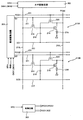
次に、本発明の第1の実施形態に係るアクティブマトリクス型の有機EL表示装置について、図面を参照して説明する。図1は、この有機EL表示装置の等価回路図である。図1は、表示パネルにマトリクス状に配置された複数の画素の中から、第1行目の画素210Aと第2行目の画素210Bだけを示している。画素210A、210Bは列方向に互いに隣接している。なお、図1において、図9と同一の構成部分については同一の符号を付してその説明を省略する。以下では、画素選択用TFT213及びプリチャージ用TFT220はNチャネル型であり、駆動用TFT214はPチャネル型であるとして説明をするが、もちろん、本発明はこれらのチャネル型に限られることはない。
Next, an active matrix organic EL display device according to a first embodiment of the present invention will be described with reference to the drawings. FIG. 1 is an equivalent circuit diagram of the organic EL display device. FIG. 1 shows only a
画素210Aにおいて、駆動用TFT214のソースとゲートの間にプリチャージ用TFT220が接続されている。このプリチャージ用TFT220のゲートはプリチャージ信号線221に接続されている。プリチャージ信号線221にはプリチャージパルス信号PCG1が供給されるので、プリチャージ用TFT220はこのプリチャージパルス信号PCG1に応じてスイッチングする。プリチャージ用TFT220がオンすると、駆動用TFT214のソースとゲートとは短絡される。これにより、駆動用TFT214のソース電位とゲート電位はともに正電源電位PVddに設定されるので、駆動用TFT214はオフする。プリチャージ用TFT220がオフすると、駆動用TFT214のソースとゲートとは電気的に絶縁されることになる。保持容量線217には固定電位ではなく、後述する所定の期間にハイレベルになる保持容量制御パルス信号SC1が供給される。
In the
画素210Bも同様に構成されているが、プリチャージ信号線221にはプリチャージパルス信号PCG2が供給され、保持容量線217には保持容量制御パルス信号SC2が供給される。
The
垂直駆動回路301は、垂直走査を開始する基準信号である垂直スタートパルス信号STVを相補的な垂直クロックCKV1,CKV2に同期してシフトして、画素選択信号G1,G2を生成する。画素選択信号G1は画素選択信号線211を通して画素210Aの画素選択用TFT213のゲートに印加され、画素選択信号G2は画素選択信号線211を通して画素210Bの画素選択用TFT213のゲートに印加される。イネーブル信号ENBは画素選択信号G1が画素選択信号線211に出力されるタイミングを制御する信号であり、画素選択信号G1,G2の重なりを防止するために用いられる。
The
水平駆動回路302は、水平スタートパルス信号STHを相補的な水平クロックCKH1,CKH2に同期してシフトして、水平走査信号を生成する。そして、水平駆動回路302は、この水平走査信号に同期して表示信号Dを表示信号線212に出力する。
The
制御回路303は、垂直スタートパルス信号STVの立ち下がりに同期して、前記プリチャージパルス信号PCG1、PCG2及び前記保持容量制御パルス信号SC1、SC2を生成する回路である。図1では、制御回路303は、垂直駆動回路301に外部に配置されているが、垂直駆動回路301の内部に設けてもよい。
The
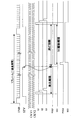
次に、上述した有機EL表示装置の駆動方法について、図面を参照して説明する。図2は、本実施形態に係る表示装置の駆動方法を説明するタイミング図である。垂直スタートパルス信号STVの立ち上がりに同期して、垂直駆動回路301からの画素選択信号G1,G2,G3が次々にパルス出力される。
Next, a method for driving the above-described organic EL display device will be described with reference to the drawings. FIG. 2 is a timing diagram illustrating a method for driving the display device according to the present embodiment. In synchronization with the rise of the vertical start pulse signal STV, the pixel selection signals G1, G2, and G3 from the
第1行目の画素に着目すると、ハイレベルの画素選択信号G1に応じて、第1行目の画素210Aの画素選択用TFT213が1水平期間オンし、この期間に水平駆動回路302から表示信号Dが表示信号線212に出力され、画素選択用TFT213を通して駆動用TFT214のゲートに印加されると共に、保持容量218によって保持される。即ち、表示信号Dが画素210Aに書き込まれる。そして、駆動用TFT214のゲートに印加された表示信号Dに応じて、駆動用TFT214がオン状態となる場合には、そのコンダクタンスに応じた電流が駆動用TFT214を通して有機EL素子216に供給され、有機EL素子216がそれに応じた輝度で発光する。
Focusing on the pixels in the first row, the
1水平期間が終わり、画素選択信号G1がロウレベルに戻ると、画素選択用TFT213はオフするが、表示信号Dは保持容量218によって保持されているので、有機EL素子216の発光期間は継続される。即ち、第1行目の画素については画素選択信号G1の立ち上がりに応じて発光期間が開始し、第2行目の画素については画素選択信号G2の立ち上がりに応じて発光期間が開始し、第3行目の画素については画素選択信号G3の立ち上がりに応じて発光期間が開始することになる。
When one horizontal period ends and the pixel selection signal G1 returns to the low level, the
その後、垂直スタートパルス信号STVの立ち下がりに同期して、制御回路303からプリチャージパルス信号PCG1、PCG2及び保持容量制御パルス信号SC1、SC2が次々と出力される。第1行目の画素に着目すると、ハイレベルのプリチャージパルス信号PCG1に応じて、プリチャージ用TFT220がオンする。すると、駆動用TFT214のソースとゲートとは短絡され、駆動用TFT214のゲート電位はソース電位と同じ正電源電位PVddとなり、駆動用TFT214はオフする。これにより、有機EL素子216は消灯するので、これで発光期間は終了し、消灯期間が開始し、この消灯期間は次の1垂直期間に画素選択信号G1がハイレベルに立ち上がるまで継続される。
Thereafter, in synchronization with the fall of the vertical start pulse signal STV, the precharge pulse signals PCG1 and PCG2 and the storage capacitor control pulse signals SC1 and SC2 are successively output from the
その後、プリチャージパルス信号PCG1がロウレベルに変化すると、プリチャージ用TFT220がオフして駆動用TFT214のソースとゲートの間は絶縁される。その後あるいは同時に、保持容量制御パルス信号SC1がハイレベルに立ち上がる。すると、保持容量218の容量結合効果により、駆動用TFT214のゲートの電位が保持容量制御パルス信号SC1のロウレベルからハイレベルへの電圧変化分ΔV(例えば、約10V)に応じて上昇する。
Thereafter, when the precharge pulse signal PCG1 changes to a low level, the
これにより、駆動用TFT214のゲート電位が、そのソース電位に比して高くなる。駆動用TFT214のゲート絶縁膜に、前回の表示信号Dの書き込みにより、キャリア(正孔)がトラップされていたとすると、そのキャリア(正孔)はゲートからソースあるいはドレインへ向かう電界によりトンネル電流となって、ゲート絶縁膜からソースあるいはドレインに引き抜かれる。これにより、駆動用TFT214の電気的特性が初期化される。これにより、駆動用TFT214には、次のフレーム期間に画素に表示信号Dを書き込む際に、その表示信号Dに応じた適正な電流値の電流が流れるようになる。
As a result, the gate potential of the driving
第2行目の画素についても同様であり、画素選択信号G2の立ち上がりから発光期間が開始する。そして、第1行目のプリチャージパルス信号PCG1がロウレベルに変化した後、第2行目のプリチャージパルス信号PCG2が立ち上がり、プリチャージ用TFT220がオンする。その後、プリチャージパルス信号PCG2がロウレベルに変化すると、プリチャージ用TFT220がオフして駆動用TFT214のソースとゲートの間は絶縁される。その後あるいは同時に、保持容量制御パルス信号SC2がハイレベルに立ち上がる。すると、保持容量218の容量結合効果により、駆動用TFT214のゲートの電位が保持容量制御パルス信号SC2のロウレベルからハイレベルへの電圧変化分ΔVに応じて上昇する。これにより、駆動用TFT214の電気的特性が初期化される。第3行目以降の画素についても同様の動作である。
The same applies to the pixels in the second row, and the light emission period starts from the rising edge of the pixel selection signal G2. Then, after the precharge pulse signal PCG1 in the first row changes to the low level, the precharge pulse signal PCG2 in the second row rises and the
本実施形態によれば、垂直スタートパルス信号STVのパルス幅を制御することで各画素の有機EL素子216の発光期間及び消灯期間を、従来のようにマスク変更を伴うことなく、自由に調節することができる。かかる調整によって、表示パネルの表示ムラの低減、動画残像時間を低減して動画品位の向上を図ることができる。また、保持容量線217にハイレベルの保持容量制御パルス信号SC1を供給することにより、駆動用TFT214の電気的特性の初期化を最適化して、表示パネルの残像現象をさらに抑制することができる。
According to the present embodiment, by controlling the pulse width of the vertical start pulse signal STV, the light emission period and the light-off period of the
本発明の第2の実施形態に係るアクティブマトリクス型の有機EL表示装置について、図面を参照して説明する。図3は、この有機EL表示装置の等価回路図である。図3では、表示パネルにマトリクス状に配置された複数の画素の中から、第1行目の画素210Aと第2行目の画素210Bだけを示している。画素210A、210Bは列方向に互いに隣接している。なお、図3において、図9と同一の構成部分については同一の符号を付してその説明を省略する。
An active matrix organic EL display device according to a second embodiment of the present invention will be described with reference to the drawings. FIG. 3 is an equivalent circuit diagram of the organic EL display device. FIG. 3 shows only the
第1の実施形態では、垂直スタートパルス信号STVのパルス幅を利用して各画素の有機EL素子216の発光期間及び消灯期間の長さを調節するとともに、その消灯期間内に駆動用TFT214の電気的特性を初期化するというものである。これに対して、本実施形態では垂直スタートパルス信号STVを1垂直期間内に2個入力することで、2個目の垂直スタートパルス信号STVに同期して、前記プリチャージパルス信号PCG1、PCG2及び前記保持容量制御パルス信号SC1、SC2を生成して、発光期間及び消灯期間を調節するというものである。
In the first embodiment, the length of the light emission period and the light-off period of the
図3において、垂直スタートパルス信号STVのパルス数をカウントするパルスカウンタ304が設けられている。パルスカウンタ304が2個の垂直スタートパルス信号STVをカウントすると、それに基づいて、制御回路305は、プリチャージパルス信号PCG1、PCG2及び前記保持容量制御パルス信号SC1、SC2を生成する。図3では、パルスカウンタ304及び制御回路305は、垂直駆動回路301に外部に配置されているが、垂直駆動回路301の内部に設けてもよい。
In FIG. 3, a
次に、第2の実施形態の有機EL表示装置の駆動方法について、図面を参照して説明する。図4は、本実施形態に係る表示装置の駆動方法を説明するタイミング図である。1個目の垂直スタートパルス信号STVの立ち上がりに同期して、垂直駆動回路301からの画素選択信号G1,G2,G3が次々にパルス出力される。
Next, a method for driving the organic EL display device according to the second embodiment will be described with reference to the drawings. FIG. 4 is a timing diagram illustrating a method for driving the display device according to the present embodiment. In synchronization with the rise of the first vertical start pulse signal STV, the pixel selection signals G1, G2, and G3 from the
これにより、第1の実施形態と同様に、第1行目、第2行目、第3行目の画素に次々に表示信号Dが書き込まれる。そして、2個目の垂直スタートパルス信号STVがハイレベルに立ち上がると、制御回路305から第1行目のプリチャージパルス信号PCG1が出力される。このプリチャージパルス信号PCG1に応じて、プリチャージ用TFT220がオンする。その後の動作は、第1の実施形態と同様であり、プリチャージパルス信号PCG1がロウレベルに変化すると、保持容量制御パルス信号SC1がハイレベルに立ち上がる。そして、有機EL素子216の消灯期間に駆動用TFT214の電気的特性が初期化される。
Accordingly, as in the first embodiment, the display signal D is written to the pixels in the first row, the second row, and the third row one after another. When the second vertical start pulse signal STV rises to a high level, the
第2行目の画素についても同様であり、第1行目のプリチャージパルス信号PCG1がロウレベルに変化すると、第2行目のプリチャージパルス信号PCG2が立ち上がる。プリチャージパルス信号PCG2がロウレベルに変化すると、保持容量制御パルス信号SC2がハイレベルに立ち上がる。そして、有機EL素子216の消灯期間に駆動用TFT214の電気的特性が初期化される。第3行目以降の残りの画素についても同様の動作である。
The same applies to the pixels in the second row. When the precharge pulse signal PCG1 in the first row changes to a low level, the precharge pulse signal PCG2 in the second row rises. When the precharge pulse signal PCG2 changes to the low level, the storage capacitor control pulse signal SC2 rises to the high level. Then, the electrical characteristics of the driving
なお、本実施形態では2個の垂直スタートパルス信号STVが入力されているが、3個以上の垂直スタートパルス信号STVが入力されてもよい。垂直スタートパルス信号STVのパルス数をパルスカウンタ304でカウントすることで、消灯期間の長さを調節することができる。
In the present embodiment, two vertical start pulse signals STV are input, but three or more vertical start pulse signals STV may be input. By counting the number of pulses of the vertical start pulse signal STV by the
次に、本発明の第3の実施形態に係るアクティブマトリクス型の有機EL表示装置について、図面を参照して説明する。図5は、この有機EL表示装置の等価回路図である。第2の実施形態では、駆動用TFT214をオフさせるためにプリチャージ用TFT220が設けられているが、本実施形態ではプリチャージ用TFT220及びプリチャージ信号線221が除去されている。また、第2の実施形態と同様に、垂直スタートパルス信号STVのパルス数をカウントするパルスカウンタ304が設けられている。制御回路306は、パルスカウンタ304が2個の垂直スタートパルス信号STVをカウントすると、それに基づいて、保持容量制御パルス信号SC1、SC2を生成する。すなわち、本実施形態では、保持容量制御パルス信号SC1、SC2をハイレベルに活性化することにより、駆動用TFT214をオフさせるものである。
Next, an active matrix organic EL display device according to a third embodiment of the present invention will be described with reference to the drawings. FIG. 5 is an equivalent circuit diagram of the organic EL display device. In the second embodiment, a
次に、第3の実施形態の有機EL表示装置の駆動方法について、図面を参照して説明する。図6は、本実施形態に係る表示装置の駆動方法を説明するタイミング図である。1個目の垂直スタートパルス信号STVの立ち上がりに同期して、垂直駆動回路301からの画素選択信号G1,G2,G3が次々にパルス出力される。
Next, a driving method of the organic EL display device according to the third embodiment will be described with reference to the drawings. FIG. 6 is a timing diagram illustrating a method for driving the display device according to the present embodiment. In synchronization with the rise of the first vertical start pulse signal STV, the pixel selection signals G1, G2, and G3 from the
画素選択信号G1,G2,G3に応じて、第1行目、第2行目、第3行目の画素に次々に表示信号Dが書き込まれ、各行の発光期間が開始する。そして、2個目の垂直スタートパルス信号STVがハイレベルに立ち上がると、制御回路305から出力される第1行目の保持容量制御パルス信号SC1がハイレベルに立ち上がる。これにより、保持容量218の容量結合効果により、駆動用TFT214のゲートの電位が保持容量制御パルス信号SC1のロウレベルからハイレベルへの電圧変化分ΔVに応じて上昇する。この電圧変化分ΔVが十分に大きければPチャネル型の駆動用TFT214がオフし、有機EL素子216の消灯期間が開始する。具体的には、Vs−Vg<Vtが成り立てば、駆動用TFT214はオフする。Vsは駆動用TFT214のソース電位であり、正電源電位PVddである。Vgは電圧変化分ΔVの受けて上昇したゲート電位、Vtは駆動用TFT214の閾値(threshold voltage)の絶対値である。
In response to the pixel selection signals G1, G2, and G3, the display signals D are sequentially written to the pixels in the first row, the second row, and the third row, and the light emission period of each row starts. When the second vertical start pulse signal STV rises to a high level, the storage capacitor control pulse signal SC1 of the first row output from the
そして、次の1垂直期間の開始時に発生するイネーブル信号ENBの立ち上がりからの所定の遅延時間後に、保持容量制御パルス信号SC1はハイレベルからロウレベルへ変化し、消灯期間が終了するように設定されている。 Then, after a predetermined delay time from the rise of the enable signal ENB generated at the start of the next one vertical period, the storage capacitor control pulse signal SC1 changes from the high level to the low level, and the extinguishing period is set to end. Yes.
第2行目の画素についても同様であり、1行目の保持容量制御パルス信号SC1がハイレベルに立ち上がった後に、2行目の保持容量制御パルス信号SC2がハイレベルに立ち上がり、第2行目の画素の発光期間が終了して消灯期間が開始する。また、第3行目の画素についても同様であり、2行目の保持容量制御パルス信号SC2がハイレベルに立ち上がった後に、第3行目の保持容量制御パルス信号SC3がハイレベルに立ち上がり、第3行目の画素の発光期間が終了して消灯期間が開始する。第4行目以降の残りの画素についても同様の動作である。なお、本実施形態のように、プリチャージ用TFT220及びプリチャージ信号線221を除去した構成は、第1の実施形態に対しても適用することができる。
The same applies to the pixels in the second row. After the storage capacitor control pulse signal SC1 in the first row rises to a high level, the storage capacitor control pulse signal SC2 in the second row rises to a high level, and the second row The light emission period of this pixel ends and the extinguishing period starts. The same applies to the pixels in the third row, and after the storage capacitor control pulse signal SC2 in the second row rises to a high level, the storage capacitor control pulse signal SC3 in the third row rises to a high level. The light emission period of the pixels in the third row ends and the extinguishing period starts. The same operation is performed for the remaining pixels in the fourth and subsequent rows. Note that the configuration in which the
次に、本発明の第4の実施形態に係るアクティブマトリクス型の有機EL表示装置について、図面を参照して説明する。図7は、この有機EL表示装置の等価回路図である。第2の実施形態において、駆動用TFT214はPチャネル型であるが、本実施形態ではこれをNチャネル型で構成したものである。この変更に伴い、プリチャージ用TFT225の接続箇所も図7のように変更されている。
Next, an active matrix organic EL display device according to a fourth embodiment of the present invention will be described with reference to the drawings. FIG. 7 is an equivalent circuit diagram of the organic EL display device. In the second embodiment, the driving
次に、第4の実施形態の有機EL表示装置の駆動方法について、図面を参照して説明する。図8は、本実施形態に係る表示装置の駆動方法を説明するタイミング図である。1個目の垂直スタートパルス信号STVの立ち上がりに同期して、垂直駆動回路301からの画素選択信号G1,G2,G3が次々にパルス出力される。
Next, a driving method of the organic EL display device according to the fourth embodiment will be described with reference to the drawings. FIG. 8 is a timing diagram illustrating a method for driving the display device according to the present embodiment. In synchronization with the rise of the first vertical start pulse signal STV, the pixel selection signals G1, G2, and G3 from the
これにより、第2の実施形態と同様に、第1行目、第2行目、第3行目の画素に次々に表示信号Dが書き込まれ、各行の発光期間が開始する。そして、2個目の垂直スタートパルス信号STVがハイレベルに立ち上がると、制御回路307から第1行目のプリチャージパルス信号PCG1が出力される。
As a result, as in the second embodiment, the display signal D is sequentially written to the pixels in the first row, the second row, and the third row, and the light emission period of each row starts. When the second vertical start pulse signal STV rises to a high level, the
このプリチャージパルス信号PCG1に応じて、プリチャージ用TFT225がオンする。すると、駆動用TFT214のソースとゲートとは短絡され、駆動用TFT214のゲート電位はソース電位と同じ電位となり、駆動用TFT214はオフする。これにより、有機EL素子216は消灯するので、これで発光期間は終了し、消灯期間が開始し、この消灯期間は次の1垂直期間に画素選択信号G1がハイレベルに立ち上がるまで継続される。なお、このように、駆動用TFT214をNチャネル型で構成する点は第1の実施形態にも適用することができる。
In response to the precharge pulse signal PCG1, the
次に、本発明の第5の実施形態に係るアクティブマトリクス型の有機EL表示装置について、図面を参照して説明する。図10は、有機EL表示装置の等価回路図である。本実施形態は、第3の実施形態と同様に、プリチャージ用TFT220及びプリチャージ信号線221が除去されている。第3の実施形態と異なるのは、垂直スタートパルス信号STVのパルス数をカウントするパルスカウンタ304が設けられていない点である。そして、制御回路308は、垂直スタートパルス信号STVの立ち下がりに同期して、保持容量制御パルス信号SC1、SC2を生成する。これらの保持容量制御パルス信号SC1、SC2をハイレベルに活性化することにより、駆動用TFT214をオフさせ、消灯期間を開始させる。
Next, an active matrix organic EL display device according to a fifth embodiment of the present invention will be described with reference to the drawings. FIG. 10 is an equivalent circuit diagram of the organic EL display device. In the present embodiment, as in the third embodiment, the
次に、第5の実施形態の有機EL表示装置の駆動方法について、図面を参照して説明する。図11は、本実施形態に係る表示装置の駆動方法を説明するタイミング図である。1個目の垂直スタートパルス信号STVのハイレベルへの立ち上がりに同期して、垂直駆動回路301からの画素選択信号G1,G2,G3が次々にパルス出力される。
Next, a driving method of the organic EL display device according to the fifth embodiment will be described with reference to the drawings. FIG. 11 is a timing diagram illustrating a method for driving the display device according to the present embodiment. In synchronization with the rising of the first vertical start pulse signal STV to the high level, the pixel selection signals G1, G2, and G3 from the
画素選択信号G1,G2,G3に応じて、第1行目、第2行目、第3行目の画素に次々に表示信号Dが書き込まれ、各行の発光期間が開始する。そして、垂直スタートパルス信号STVがロウレベルに立ち下がると、制御回路308から出力される第1行目の保持容量制御パルス信号SC1がハイレベルに立ち上がる。これにより、保持容量218の容量結合効果により、駆動用TFT214のゲートの電位が保持容量制御パルス信号SC1のロウレベルからハイレベルへの電圧変化分ΔVに応じて上昇する。この電圧変化分ΔVが十分に大きければPチャネル型の駆動用TFT214がオフし、有機EL素子216の消灯期間が開始する。具体的には、Vs−Vg<Vtが成り立てば、駆動用TFT214はオフする。Vsは駆動用TFT214のソース電位であり、正電源電位PVddである。Vgは電圧変化分ΔVの受けて上昇したゲート電位、Vtは駆動用TFT214の閾値(threshold voltage)の絶対値である。そして、次の1水平期間の開始時に発生するイネーブル信号ENBの立ち上がりからの所定の遅延時間後に、保持容量制御パルス信号SC1はハイレベルからロウレベルへ変化し、消灯期間が終了するように設定されている。
In response to the pixel selection signals G1, G2, and G3, the display signals D are sequentially written to the pixels in the first row, the second row, and the third row, and the light emission period of each row starts. When the vertical start pulse signal STV falls to the low level, the storage capacitor control pulse signal SC1 in the first row output from the
第2行目の画素についても同様であり、1行目の保持容量制御パルス信号SC1がハイレベルに立ち上がった後に、2行目の保持容量制御パルス信号SC2がハイレベルに立ち上がり、第2行目の画素の発光期間が終了して消灯期間が開始する。また、第3行目の画素についても同様であり、2行目の保持容量制御パルス信号SC2がハイレベルに立ち上がった後に、第3行目の保持容量制御パルス信号SC3がハイレベルに立ち上がり、第3行目の画素の発光期間が終了して消灯期間が開始する。第4行目以降の残りの画素についても同様の動作である。 The same applies to the pixels in the second row. After the storage capacitor control pulse signal SC1 in the first row rises to a high level, the storage capacitor control pulse signal SC2 in the second row rises to a high level, and the second row The light emission period of this pixel ends and the extinguishing period starts. The same applies to the pixels in the third row, and after the storage capacitor control pulse signal SC2 in the second row rises to a high level, the storage capacitor control pulse signal SC3 in the third row rises to a high level. The light emission period of the pixels in the third row ends and the extinguishing period starts. The same operation is performed for the remaining pixels in the fourth and subsequent rows.
また、上述した各実施形態は、表示装置が電圧駆動型画素回路で構成される場合を例として説明しており、各画素に供給される表示信号Dは電圧信号であるが、本発明は電流駆動型画素回路にも同様に適用することができる。この場合、表示信号Dは電流信号になる。 In each of the above embodiments, the case where the display device includes a voltage-driven pixel circuit is described as an example. The display signal D supplied to each pixel is a voltage signal. The present invention can be similarly applied to a driving pixel circuit. In this case, the display signal D is a current signal.
上述した各実施形態によれば、垂直スタートパルス信号STVを利用することにより、各画素の有機EL素子216の発光期間を自由に調節することができる。かかる調整によって、表示パネルの表示ムラの低減、残像時間を低減して動画品位の向上を図ることができる。また、表示装置の開発段階で最適な発光期間を見出すことが可能になるので、開発期間の短縮、開発コストの低減にも効果がある。さらにこのような発光期間の制御方式を表示パネルのユーザーに解放することで、ユーザーは同一仕様の表示パネルを目的に合ったアプリケーションに応用することができる。例えば、動画表示が主であるビデオカメラ用の表示パネルには、動画応答性が良いように発光期間を短くし、スチルカメラ用の表示パネルにはフリッカー防止のため、発光期間を長くすることができる。
According to each embodiment mentioned above, the light emission period of the
210,210A,210B,210C 表示画素
211 画素選択信号線 212 表示信号線 213 画素選択用TFT
214 駆動用TFT 215 電源線 216 有機EL素子
217 保持容量線 218 保持容量 220 プリチャージ用TFT
221 プリチャージ信号線 301 垂直駆動回路
302 水平駆動回路 303 制御回路 304 パルスカウンタ
305,306,307,308 制御回路
210, 210A, 210B,
214
221
305, 306, 307, 308 control circuit
Claims (7)
さらに、エッジトリガタイプの回路を使用することにより、1垂直期間に1個入力される垂直スタートパルス信号が第1のレベルから第2のレベルに変化するのを検出して前記画素選択トランジスタのゲートに印加する画素選択信号を作成すると共に、該画素選択信号を垂直クロックに同期してシフトする垂直駆動回路と、
エッジトリガタイプの回路を使用することにより、前記垂直スタートパルス信号が第2のレベルから第1のレベルに変化するのを検出して前記駆動用トランジスタをオフさせるための信号を作成すると共に、該信号を垂直クロックに同期してシフトする制御回路と、を備えることを特徴とするアクティブマトリクス型表示装置。 Each pixel includes a plurality of pixels arranged in a matrix, each pixel including a pixel selection transistor, a light emitting element, and a driving transistor for driving the light emitting element in accordance with a display signal supplied through the pixel selection transistor; With
Further, by using an edge trigger type circuit, it is detected that one vertical start pulse signal inputted in one vertical period changes from the first level to the second level, and the gate of the pixel selection transistor is detected. A vertical drive circuit that creates a pixel selection signal to be applied to and shifts the pixel selection signal in synchronization with a vertical clock ;
By using an edge trigger type circuit, a signal for detecting the change of the vertical start pulse signal from the second level to the first level and turning off the driving transistor is generated, and And a control circuit that shifts a signal in synchronization with a vertical clock .
さらに、垂直走査を開始させるための垂直スタートパルス信号に応じて、前記プリチャージパルス信号を出力して前記プリチャージ用トランジスタを所定期間オンさせる制御回路と、を備え、前記制御回路は、前記プリチャージ用トランジスタが前記所定期間の経過後にオフしたときに、前記保持容量線に保持容量制御パルス信号を出力して、前記駆動用トランジスタのゲート電位をソース電位に対して変化させることを特徴とするアクティブマトリクス型表示装置。 A plurality of pixels arranged in a matrix, each pixel including a pixel selection transistor, a light emitting element, and a driving transistor for driving the light emitting element in accordance with a display signal supplied through the pixel selection transistor; A storage capacitor connected between the gate of the driving transistor and a storage capacitor line, and for precharging that turns on in response to a precharge pulse signal and short-circuits the source and gate of the driving transistor. A transistor,
And a control circuit for outputting the precharge pulse signal and turning on the precharge transistor for a predetermined period in response to a vertical start pulse signal for starting vertical scanning. When the charging transistor is turned off after the lapse of the predetermined period, a storage capacitor control pulse signal is output to the storage capacitor line, and the gate potential of the driving transistor is changed with respect to the source potential. Active matrix display device.
さらに、垂直走査を開始させるための垂直スタートパルス信号に応じて、前記プリチャージパルス信号を出力して前記プリチャージ用トランジスタを所定期間オンさせる制御回路と、を備え、前記制御回路は、前記垂直スタートパルス信号が第1のレベルから第2のレベルに変化するのに応じて前記プリチャージパルス信号を出力することを特徴とするアクティブマトリクス型表示装置。 A plurality of pixels arranged in a matrix, each pixel including a pixel selection transistor, a light emitting element, and a driving transistor for driving the light emitting element in accordance with a display signal supplied through the pixel selection transistor; A storage capacitor connected between the gate of the driving transistor and a storage capacitor line, and for precharging that turns on in response to a precharge pulse signal and short-circuits the source and gate of the driving transistor. A transistor,
And a control circuit for outputting the precharge pulse signal and turning on the precharge transistor for a predetermined period in response to a vertical start pulse signal for starting vertical scanning. An active matrix display device, wherein the precharge pulse signal is output in response to a start pulse signal changing from a first level to a second level.
さらに、エッジトリガタイプの回路を使用することにより、1垂直期間に1個入力される垂直スタートパルス信号が第1のレベルから第2のレベルに変化するのを検出して前記画素選択トランジスタのゲートに印加する画素選択信号を作成すると共に、該画素選択信号を垂直クロックに同期してシフトする垂直駆動回路と、
エッジトリガタイプの回路を使用することにより、前記垂直スタートパルス信号が第2のレベルから第1のレベルに変化するのを検出して保持容量制御パルス信号を作成し、該保持容量制御パルス信号を前記保持容量線に出力することにより前記駆動用トランジスタがオフするようにそのゲート電圧をソース電圧に対して変化させると共に、該保持容量制御パルス信号を垂直クロックに同期してシフトする制御回路を備えることを特徴とするアクティブマトリクス型表示装置。 A plurality of pixels arranged in a matrix, each pixel including a pixel selection transistor, a light emitting element, and a driving transistor for driving the light emitting element in accordance with a display signal supplied through the pixel selection transistor; A storage capacitor connected between the gate of the driving transistor and a storage capacitor line and holding the display signal;
Further, by using an edge trigger type circuit, it is detected that one vertical start pulse signal inputted in one vertical period changes from the first level to the second level, and the gate of the pixel selection transistor is detected. A vertical drive circuit that creates a pixel selection signal to be applied to and shifts the pixel selection signal in synchronization with a vertical clock ;
By using an edge trigger type circuit, a change in the vertical start pulse signal from the second level to the first level is detected and a retention capacitor control pulse signal is generated. A control circuit is provided that changes the gate voltage with respect to the source voltage so that the driving transistor is turned off by outputting to the storage capacitor line, and shifts the storage capacitor control pulse signal in synchronization with the vertical clock. An active matrix display device characterized by the above.
Priority Applications (4)
| Application Number | Priority Date | Filing Date | Title |
|---|---|---|---|
| JP2006027915A JP4986468B2 (en) | 2005-03-11 | 2006-02-06 | Active matrix display device |
| TW095106943A TWI345212B (en) | 2005-03-11 | 2006-03-02 | Active matrix type display device |
| KR1020060022134A KR20060097657A (en) | 2005-03-11 | 2006-03-09 | Active matrix type display device |
| US11/372,487 US7623102B2 (en) | 2005-03-11 | 2006-03-10 | Active matrix type display device |
Applications Claiming Priority (3)
| Application Number | Priority Date | Filing Date | Title |
|---|---|---|---|
| JP2005068813 | 2005-03-11 | ||
| JP2005068813 | 2005-03-11 | ||
| JP2006027915A JP4986468B2 (en) | 2005-03-11 | 2006-02-06 | Active matrix display device |
Publications (2)
| Publication Number | Publication Date |
|---|---|
| JP2006285210A JP2006285210A (en) | 2006-10-19 |
| JP4986468B2 true JP4986468B2 (en) | 2012-07-25 |
Family
ID=37034680
Family Applications (1)
| Application Number | Title | Priority Date | Filing Date |
|---|---|---|---|
| JP2006027915A Active JP4986468B2 (en) | 2005-03-11 | 2006-02-06 | Active matrix display device |
Country Status (4)
| Country | Link |
|---|---|
| US (1) | US7623102B2 (en) |
| JP (1) | JP4986468B2 (en) |
| KR (1) | KR20060097657A (en) |
| TW (1) | TWI345212B (en) |
Families Citing this family (15)
| Publication number | Priority date | Publication date | Assignee | Title |
|---|---|---|---|---|
| TWI327720B (en) * | 2005-03-11 | 2010-07-21 | Sanyo Electric Co | Active matrix type display device and driving method thereof |
| JP2006251453A (en) * | 2005-03-11 | 2006-09-21 | Sanyo Electric Co Ltd | Active matrix type display device and method for driving the same |
| JP5656321B2 (en) * | 2005-10-18 | 2015-01-21 | 株式会社半導体エネルギー研究所 | Semiconductor device, display device, display module, and electronic apparatus |
| KR101324756B1 (en) | 2005-10-18 | 2013-11-05 | 가부시키가이샤 한도오따이 에네루기 켄큐쇼 | Display device and driving method thereof |
| KR20070059403A (en) * | 2005-12-06 | 2007-06-12 | 삼성전자주식회사 | Display device and driving method thereof |
| KR100858618B1 (en) | 2007-04-10 | 2008-09-17 | 삼성에스디아이 주식회사 | Organic light emitting display and driving method thereof |
| US8648776B2 (en) * | 2008-05-20 | 2014-02-11 | Sharp Kabushiki Kaisha | Display device, pixel circuit, and method for driving same |
| US9280930B2 (en) * | 2009-05-20 | 2016-03-08 | Dialog Semiconductor Gmbh | Back to back pre-charge scheme |
| KR20140044578A (en) | 2012-10-05 | 2014-04-15 | 삼성디스플레이 주식회사 | Pixel, display device and driving method thereof |
| JP2014002417A (en) * | 2013-09-24 | 2014-01-09 | Semiconductor Energy Lab Co Ltd | Semiconductor device, display device, display module and electronic apparatus |
| KR102228146B1 (en) * | 2014-11-12 | 2021-03-18 | 삼성디스플레이 주식회사 | Power suplly device and display device having the same |
| CN107331358B (en) * | 2017-07-19 | 2019-11-15 | 深圳市华星光电半导体显示技术有限公司 | A kind of display panel and display panel grid signal control method |
| TWI689913B (en) * | 2018-12-25 | 2020-04-01 | 友達光電股份有限公司 | Display device |
| JP2019066896A (en) * | 2019-02-05 | 2019-04-25 | 株式会社半導体エネルギー研究所 | Semiconductor device |
| JP2020112821A (en) * | 2020-03-30 | 2020-07-27 | 株式会社半導体エネルギー研究所 | Semiconductor device |
Family Cites Families (25)
| Publication number | Priority date | Publication date | Assignee | Title |
|---|---|---|---|---|
| KR0156804B1 (en) * | 1995-11-28 | 1998-12-15 | 김광호 | A start pulse vertical signal doing free-charge independent of bios using data enable signal |
| JP3259774B2 (en) * | 1999-06-09 | 2002-02-25 | 日本電気株式会社 | Image display method and apparatus |
| JP4092857B2 (en) * | 1999-06-17 | 2008-05-28 | ソニー株式会社 | Image display device |
| JP4212079B2 (en) | 2000-01-11 | 2009-01-21 | ローム株式会社 | Display device and driving method thereof |
| JP4106865B2 (en) | 2000-12-07 | 2008-06-25 | ソニー株式会社 | Active matrix display device and portable terminal |
| WO2002047062A1 (en) * | 2000-12-08 | 2002-06-13 | Matsushita Electric Industrial Co., Ltd. | El display device |
| JP4027614B2 (en) * | 2001-03-28 | 2007-12-26 | 株式会社日立製作所 | Display device |
| JP4869497B2 (en) * | 2001-05-30 | 2012-02-08 | 株式会社半導体エネルギー研究所 | Display device |
| WO2003027997A1 (en) * | 2001-09-21 | 2003-04-03 | Semiconductor Energy Laboratory Co., Ltd. | Display apparatus and its driving method |
| AU2002349965A1 (en) | 2001-10-19 | 2003-04-28 | Clare Micronix Integrated Systems, Inc. | Circuit for predictive control of boost current in a passive matrix oled display and method therefor |
| US7167169B2 (en) | 2001-11-20 | 2007-01-23 | Toppoly Optoelectronics Corporation | Active matrix oled voltage drive pixel circuit |
| JP2003345307A (en) * | 2002-05-23 | 2003-12-03 | Sharp Corp | Display device and its driving method |
| JP4123084B2 (en) * | 2002-07-31 | 2008-07-23 | セイコーエプソン株式会社 | Electronic circuit, electro-optical device, and electronic apparatus |
| JP2004157437A (en) * | 2002-11-08 | 2004-06-03 | Sony Corp | Display device |
| WO2004061809A1 (en) * | 2002-12-27 | 2004-07-22 | Semiconductor Energy Laboratory Co., Ltd. | Semiconductor device, light-emitting display apparatus, and method for driving them |
| JP4023335B2 (en) | 2003-02-19 | 2007-12-19 | セイコーエプソン株式会社 | Electro-optical device, driving method of electro-optical device, and electronic apparatus |
| JP2004341435A (en) | 2003-05-19 | 2004-12-02 | Toshiba Matsushita Display Technology Co Ltd | Active matrix type display device and driving method for active matrix type display device |
| US8537081B2 (en) * | 2003-09-17 | 2013-09-17 | Hitachi Displays, Ltd. | Display apparatus and display control method |
| JP4836402B2 (en) | 2003-09-29 | 2011-12-14 | 東北パイオニア株式会社 | Self-luminous display device |
| JP4180018B2 (en) | 2003-11-07 | 2008-11-12 | 三洋電機株式会社 | Pixel circuit and display device |
| US7333102B2 (en) | 2003-12-31 | 2008-02-19 | Intel Corporation | Self-configured display power supply |
| US8013809B2 (en) | 2004-06-29 | 2011-09-06 | Semiconductor Energy Laboratory Co., Ltd. | Display device and driving method of the same, and electronic apparatus |
| TWI288902B (en) | 2004-06-30 | 2007-10-21 | Au Optronics Corp | Active matrix organic light emitting diode (AMOLED) display, a pixel driving circuit, and a driving method thereof |
| JP2006251453A (en) | 2005-03-11 | 2006-09-21 | Sanyo Electric Co Ltd | Active matrix type display device and method for driving the same |
| TWI327720B (en) | 2005-03-11 | 2010-07-21 | Sanyo Electric Co | Active matrix type display device and driving method thereof |
-
2006
- 2006-02-06 JP JP2006027915A patent/JP4986468B2/en active Active
- 2006-03-02 TW TW095106943A patent/TWI345212B/en active
- 2006-03-09 KR KR1020060022134A patent/KR20060097657A/en not_active Application Discontinuation
- 2006-03-10 US US11/372,487 patent/US7623102B2/en active Active
Also Published As
| Publication number | Publication date |
|---|---|
| TWI345212B (en) | 2011-07-11 |
| US7623102B2 (en) | 2009-11-24 |
| KR20060097657A (en) | 2006-09-14 |
| TW200632853A (en) | 2006-09-16 |
| JP2006285210A (en) | 2006-10-19 |
| US20060214889A1 (en) | 2006-09-28 |
Similar Documents
| Publication | Publication Date | Title |
|---|---|---|
| JP4986468B2 (en) | Active matrix display device | |
| JP6710251B2 (en) | Organic light emitting display device and driving method thereof | |
| EP3343552B1 (en) | Electroluminescent display | |
| JP6080286B2 (en) | Organic light emitting display device and driving method thereof | |
| JP4398413B2 (en) | Pixel drive circuit with threshold voltage compensation | |
| JP5230806B2 (en) | Image display device and driving method thereof | |
| US20110122324A1 (en) | Display apparatus, method of driving the display device, and electronic device | |
| US20060208976A1 (en) | Active matrix type display device and driving method thereof | |
| JP2006133731A (en) | Light emitting display and driving method thereof | |
| JP2011520138A (en) | Pixel circuit, display system, and driving method thereof | |
| JP2011112724A (en) | Display device, method of driving the same and electronic equipment | |
| KR102423662B1 (en) | Display panel | |
| JP2008262143A (en) | Organic light emitting display and method for driving organic light-emitting display using the same | |
| WO2016070506A1 (en) | Amoled drive apparatus and drive method | |
| JP2011112722A (en) | Display device, method of driving the same and electronic equipment | |
| JP2011135523A (en) | Drive circuit and display device | |
| KR20180003390A (en) | Organic light emitting display device and driving method of the same | |
| JP2009271500A (en) | Organic electroluminescent display device and driving method of the same | |
| JP2011022462A (en) | Display device, driving method therefor, and electronics device | |
| KR100659622B1 (en) | Display device | |
| JP2011150270A (en) | Drive circuit and display device | |
| JP2011154287A (en) | Display device, method of driving the same, and electronic device | |
| JP5532301B2 (en) | Driving circuit and display device | |
| KR100836431B1 (en) | Pixel and organic light emitting display device using the pixel | |
| JP2007004035A (en) | Active matrix display device and method of driving active matrix display device |
Legal Events
| Date | Code | Title | Description |
|---|---|---|---|
| A621 | Written request for application examination |
Free format text: JAPANESE INTERMEDIATE CODE: A621 Effective date: 20090130 |
|
| A977 | Report on retrieval |
Free format text: JAPANESE INTERMEDIATE CODE: A971007 Effective date: 20111011 |
|
| A131 | Notification of reasons for refusal |
Free format text: JAPANESE INTERMEDIATE CODE: A131 Effective date: 20111014 |
|
| A521 | Request for written amendment filed |
Free format text: JAPANESE INTERMEDIATE CODE: A523 Effective date: 20111206 |
|
| A131 | Notification of reasons for refusal |
Free format text: JAPANESE INTERMEDIATE CODE: A131 Effective date: 20120112 |
|
| A521 | Request for written amendment filed |
Free format text: JAPANESE INTERMEDIATE CODE: A523 Effective date: 20120306 |
|
| TRDD | Decision of grant or rejection written | ||
| A01 | Written decision to grant a patent or to grant a registration (utility model) |
Free format text: JAPANESE INTERMEDIATE CODE: A01 Effective date: 20120328 |
|
| A01 | Written decision to grant a patent or to grant a registration (utility model) |
Free format text: JAPANESE INTERMEDIATE CODE: A01 |
|
| A61 | First payment of annual fees (during grant procedure) |
Free format text: JAPANESE INTERMEDIATE CODE: A61 Effective date: 20120424 |
|
| R151 | Written notification of patent or utility model registration |
Ref document number: 4986468 Country of ref document: JP Free format text: JAPANESE INTERMEDIATE CODE: R151 |
|
| FPAY | Renewal fee payment (event date is renewal date of database) |
Free format text: PAYMENT UNTIL: 20150511 Year of fee payment: 3 |