JP2011112724A - Display device, method of driving the same and electronic equipment - Google Patents
Display device, method of driving the same and electronic equipment Download PDFInfo
- Publication number
- JP2011112724A JP2011112724A JP2009266735A JP2009266735A JP2011112724A JP 2011112724 A JP2011112724 A JP 2011112724A JP 2009266735 A JP2009266735 A JP 2009266735A JP 2009266735 A JP2009266735 A JP 2009266735A JP 2011112724 A JP2011112724 A JP 2011112724A
- Authority
- JP
- Japan
- Prior art keywords
- gate
- transistor
- voltage
- pixel circuit
- display device
- Prior art date
- Legal status (The legal status is an assumption and is not a legal conclusion. Google has not performed a legal analysis and makes no representation as to the accuracy of the status listed.)
- Pending
Links
Images


Classifications
-
- G—PHYSICS
- G09—EDUCATION; CRYPTOGRAPHY; DISPLAY; ADVERTISING; SEALS
- G09G—ARRANGEMENTS OR CIRCUITS FOR CONTROL OF INDICATING DEVICES USING STATIC MEANS TO PRESENT VARIABLE INFORMATION
- G09G3/00—Control arrangements or circuits, of interest only in connection with visual indicators other than cathode-ray tubes
- G09G3/20—Control arrangements or circuits, of interest only in connection with visual indicators other than cathode-ray tubes for presentation of an assembly of a number of characters, e.g. a page, by composing the assembly by combination of individual elements arranged in a matrix no fixed position being assigned to or needed to be assigned to the individual characters or partial characters
- G09G3/22—Control arrangements or circuits, of interest only in connection with visual indicators other than cathode-ray tubes for presentation of an assembly of a number of characters, e.g. a page, by composing the assembly by combination of individual elements arranged in a matrix no fixed position being assigned to or needed to be assigned to the individual characters or partial characters using controlled light sources
- G09G3/30—Control arrangements or circuits, of interest only in connection with visual indicators other than cathode-ray tubes for presentation of an assembly of a number of characters, e.g. a page, by composing the assembly by combination of individual elements arranged in a matrix no fixed position being assigned to or needed to be assigned to the individual characters or partial characters using controlled light sources using electroluminescent panels
- G09G3/32—Control arrangements or circuits, of interest only in connection with visual indicators other than cathode-ray tubes for presentation of an assembly of a number of characters, e.g. a page, by composing the assembly by combination of individual elements arranged in a matrix no fixed position being assigned to or needed to be assigned to the individual characters or partial characters using controlled light sources using electroluminescent panels semiconductive, e.g. using light-emitting diodes [LED]
- G09G3/3208—Control arrangements or circuits, of interest only in connection with visual indicators other than cathode-ray tubes for presentation of an assembly of a number of characters, e.g. a page, by composing the assembly by combination of individual elements arranged in a matrix no fixed position being assigned to or needed to be assigned to the individual characters or partial characters using controlled light sources using electroluminescent panels semiconductive, e.g. using light-emitting diodes [LED] organic, e.g. using organic light-emitting diodes [OLED]
- G09G3/3225—Control arrangements or circuits, of interest only in connection with visual indicators other than cathode-ray tubes for presentation of an assembly of a number of characters, e.g. a page, by composing the assembly by combination of individual elements arranged in a matrix no fixed position being assigned to or needed to be assigned to the individual characters or partial characters using controlled light sources using electroluminescent panels semiconductive, e.g. using light-emitting diodes [LED] organic, e.g. using organic light-emitting diodes [OLED] using an active matrix
- G09G3/3233—Control arrangements or circuits, of interest only in connection with visual indicators other than cathode-ray tubes for presentation of an assembly of a number of characters, e.g. a page, by composing the assembly by combination of individual elements arranged in a matrix no fixed position being assigned to or needed to be assigned to the individual characters or partial characters using controlled light sources using electroluminescent panels semiconductive, e.g. using light-emitting diodes [LED] organic, e.g. using organic light-emitting diodes [OLED] using an active matrix with pixel circuitry controlling the current through the light-emitting element
-
- G—PHYSICS
- G09—EDUCATION; CRYPTOGRAPHY; DISPLAY; ADVERTISING; SEALS
- G09G—ARRANGEMENTS OR CIRCUITS FOR CONTROL OF INDICATING DEVICES USING STATIC MEANS TO PRESENT VARIABLE INFORMATION
- G09G2300/00—Aspects of the constitution of display devices
- G09G2300/04—Structural and physical details of display devices
- G09G2300/0439—Pixel structures
- G09G2300/0465—Improved aperture ratio, e.g. by size reduction of the pixel circuit, e.g. for improving the pixel density or the maximum displayable luminance or brightness
-
- G—PHYSICS
- G09—EDUCATION; CRYPTOGRAPHY; DISPLAY; ADVERTISING; SEALS
- G09G—ARRANGEMENTS OR CIRCUITS FOR CONTROL OF INDICATING DEVICES USING STATIC MEANS TO PRESENT VARIABLE INFORMATION
- G09G2300/00—Aspects of the constitution of display devices
- G09G2300/08—Active matrix structure, i.e. with use of active elements, inclusive of non-linear two terminal elements, in the pixels together with light emitting or modulating elements
- G09G2300/0809—Several active elements per pixel in active matrix panels
- G09G2300/0819—Several active elements per pixel in active matrix panels used for counteracting undesired variations, e.g. feedback or autozeroing
-
- G—PHYSICS
- G09—EDUCATION; CRYPTOGRAPHY; DISPLAY; ADVERTISING; SEALS
- G09G—ARRANGEMENTS OR CIRCUITS FOR CONTROL OF INDICATING DEVICES USING STATIC MEANS TO PRESENT VARIABLE INFORMATION
- G09G2300/00—Aspects of the constitution of display devices
- G09G2300/08—Active matrix structure, i.e. with use of active elements, inclusive of non-linear two terminal elements, in the pixels together with light emitting or modulating elements
- G09G2300/0809—Several active elements per pixel in active matrix panels
- G09G2300/0842—Several active elements per pixel in active matrix panels forming a memory circuit, e.g. a dynamic memory with one capacitor
- G09G2300/0861—Several active elements per pixel in active matrix panels forming a memory circuit, e.g. a dynamic memory with one capacitor with additional control of the display period without amending the charge stored in a pixel memory, e.g. by means of additional select electrodes
- G09G2300/0866—Several active elements per pixel in active matrix panels forming a memory circuit, e.g. a dynamic memory with one capacitor with additional control of the display period without amending the charge stored in a pixel memory, e.g. by means of additional select electrodes by means of changes in the pixel supply voltage
-
- G—PHYSICS
- G09—EDUCATION; CRYPTOGRAPHY; DISPLAY; ADVERTISING; SEALS
- G09G—ARRANGEMENTS OR CIRCUITS FOR CONTROL OF INDICATING DEVICES USING STATIC MEANS TO PRESENT VARIABLE INFORMATION
- G09G2320/00—Control of display operating conditions
- G09G2320/06—Adjustment of display parameters
- G09G2320/0606—Manual adjustment
Landscapes
- Engineering & Computer Science (AREA)
- Physics & Mathematics (AREA)
- Computer Hardware Design (AREA)
- General Physics & Mathematics (AREA)
- Theoretical Computer Science (AREA)
- Electroluminescent Light Sources (AREA)
- Control Of El Displays (AREA)
- Control Of Indicators Other Than Cathode Ray Tubes (AREA)
Abstract
Description
本発明は、画素ごとに配置した発光素子で画像を表示する表示装置およびその駆動方法に関する。また、本発明は、上記表示装置を備えた電子機器に関する。 The present invention relates to a display device that displays an image with a light emitting element arranged for each pixel and a driving method thereof. Moreover, this invention relates to the electronic device provided with the said display apparatus.
近年、画像表示を行う表示装置の分野では、画素の発光素子として、流れる電流値に応じて発光輝度が変化する電流駆動型の光学素子、例えば有機EL(electro luminescence)素子を用いた表示装置が開発され、商品化が進められている。 In recent years, in the field of display devices that perform image display, display devices that use current-driven optical elements, such as organic EL (electroluminescence) elements, whose light emission luminance changes according to the value of a flowing current are used as light emitting elements of pixels. Developed and commercialized.
有機EL素子は、液晶素子などと異なり自発光素子である。そのため、有機EL素子を用いた表示装置(有機EL表示装置)では、光源(バックライト)が必要ないので、光源を必要とする液晶表示装置と比べて画像の視認性が高く、消費電力が低く、かつ素子の応答速度が速い。 Unlike a liquid crystal element or the like, the organic EL element is a self-luminous element. Therefore, a display device (organic EL display device) using an organic EL element does not require a light source (backlight), and thus has higher image visibility and lower power consumption than a liquid crystal display device that requires a light source. And the response speed of the element is fast.
有機EL表示装置では、液晶表示装置と同様、その駆動方式として単純(パッシブ)マトリクス方式とアクティブマトリクス方式とがある。前者は、構造が単純であるものの、大型かつ高精細の表示装置の実現が難しいなどの問題がある。そのため、現在では、アクティブマトリクス方式の開発が盛んに行なわれている。この方式は、画素ごとに配した有機EL素子に流れる電流を、有機EL素子ごとに設けた画素回路内に設けた能動素子(一般にはTFT(Thin Film Transistor;薄膜トランジスタ))によって制御するものである。 In the organic EL display device, similarly to the liquid crystal display device, there are a simple (passive) matrix method and an active matrix method as its driving method. Although the former has a simple structure, there is a problem that it is difficult to realize a large-sized and high-definition display device. For this reason, active matrix systems are currently being actively developed. In this method, a current flowing through an organic EL element arranged for each pixel is controlled by an active element (generally a TFT (Thin Film Transistor)) provided in a pixel circuit provided for each organic EL element. .
一般的に、有機EL素子の電流−電圧(I−V)特性は、時間の経過に従って劣化(経時劣化)する。有機EL素子を電流駆動する画素回路では、有機EL素子のI−V特性が経時変化すると、有機EL素子と、有機EL素子に直列に接続されたTFTとの分圧比が変化するので、TFTのゲート−ソース間電圧Vgsも変化する。その結果、TFTに流れる電流値が変化するので、有機EL素子に流れる電流値も変化し、その電流値に応じて発光輝度も変化する。 Generally, the current-voltage (IV) characteristics of an organic EL element deteriorate (deteriorate with time) as time passes. In the pixel circuit that current-drives the organic EL element, when the IV characteristic of the organic EL element changes with time, the voltage division ratio between the organic EL element and the TFT connected in series to the organic EL element changes. The gate-source voltage V gs also changes. As a result, since the current value flowing through the TFT changes, the current value flowing through the organic EL element also changes, and the light emission luminance also changes according to the current value.
また、TFTにおいて、閾値電圧Vthや移動度μが経時的に変化したり、製造プロセスのばらつきによって画素回路ごとに異なったりする場合がある。TFTの閾値電圧Vthや移動度μが画素回路ごとに異なる場合には、TFTに流れる電流値が画素回路ごとにばらつく。その結果、TFTのゲートに同じ電圧を印加しても、有機EL素子の発光輝度がばらつき、画面の一様性(ユニフォーミティ)が損なわれる。 Further, in the TFT, the threshold voltage V th and the mobility μ may change with time, or may vary from pixel circuit to pixel circuit due to manufacturing process variations. When the threshold voltage V th and the mobility μ of the TFT are different for each pixel circuit, the value of the current flowing through the TFT varies for each pixel circuit. As a result, even when the same voltage is applied to the gate of the TFT, the light emission luminance of the organic EL element varies and the uniformity of the screen is lost.
そこで、有機EL素子のI−V特性が経時変化したり、TFTの閾値電圧Vthや移動度μが経時変化したりしても、それらの影響を受けることなく、有機EL素子の発光輝度を一定に保つようにするために、TFTの閾値電圧Vthや移動度μを補正する方策が提案されている(例えば、特許文献1参照)。 Therefore, even if the IV characteristic of the organic EL element changes with time, or the threshold voltage V th or mobility μ of the TFT changes with time, the light emission luminance of the organic EL element is not affected by them. In order to keep it constant, a method for correcting the threshold voltage V th and mobility μ of the TFT has been proposed (see, for example, Patent Document 1).
ところで、有機EL表示装置の分野では、他の表示装置の分野と同様、低消費電力化が強く要求されている。低消費電力化を実現する方策として、例えば、TFTのサイズを大きくして、TFTのゲート−ソース間電圧Vgsを低減することが考えられる。しかし、TFTのサイズを大きくすることは、高精細化の流れに反することになるので、TFTのサイズ拡大には限界がある。 By the way, in the field of organic EL display devices, as in other display device fields, low power consumption is strongly demanded. As a measure for realizing low power consumption, for example, it is conceivable to increase the size of the TFT to reduce the gate-source voltage V gs of the TFT. However, increasing the size of the TFT is against the trend toward higher definition, so there is a limit to the increase in size of the TFT.
本発明はかかる問題点に鑑みてなされたもので、その目的は、高精細化を阻害することなく、低消費電力化を実現することの可能な表示装置およびその駆動方法ならびに電子機器を提供することにある。 The present invention has been made in view of such problems, and an object thereof is to provide a display device capable of realizing low power consumption without hindering high definition, a driving method thereof, and an electronic apparatus. There is.
本発明の表示装置は、一組の発光素子および画素回路が2次元配置された表示部と、映像信号に基づいて画素回路を駆動する駆動部とを備えたものである。画素回路は、2つのトランジスタ(第1トランジスタ,第2トランジスタ)を有している。第1トランジスタは、第1ゲートおよび第2ゲートを含んでおり、発光素子に流れる電流を制御するデュアルゲート型のトランジスタである。一方、第2トランジスタは、映像信号に応じた信号電圧を第1ゲートに書き込むトランジスタである。駆動部は、第1トランジスタのゲート−ソース間電圧の値として採りうる範囲の少なくとも一部が5V以下となるように、信号電圧を前記画素回路に印加するようになっている。 The display device of the present invention includes a display unit in which a set of light emitting elements and pixel circuits are two-dimensionally arranged, and a drive unit that drives the pixel circuits based on a video signal. The pixel circuit has two transistors (a first transistor and a second transistor). The first transistor includes a first gate and a second gate, and is a dual gate type transistor that controls a current flowing through the light emitting element. On the other hand, the second transistor is a transistor that writes a signal voltage corresponding to the video signal to the first gate. The driving unit applies a signal voltage to the pixel circuit so that at least a part of a range that can be taken as a gate-source voltage value of the first transistor is 5 V or less.
本発明の電子機器は、上記表示装置を備えたものである。 An electronic apparatus according to the present invention includes the display device.
本発明の表示装置の駆動方法は、以下の2つのステップを含むものである。
(A)以下の構成を備えた表示装置を用意するステップ
(B)駆動部を用いて、第1トランジスタのゲート−ソース間電圧の値として採りうる範囲の少なくとも一部が5V以下となるように、信号電圧を前記画素回路に印加するステップ
The display device driving method of the present invention includes the following two steps.
(A) Step of preparing a display device having the following configuration (B) Using the drive unit, at least a part of the range that can be taken as the value of the gate-source voltage of the first transistor is 5 V or less. Applying a signal voltage to the pixel circuit;
上記駆動方法が用いられる表示装置は、一組の発光素子および画素回路が2次元配置された表示部と、映像信号に基づいて画素回路を駆動する駆動部とを備えたものである。画素回路は、2つのトランジスタ(第1トランジスタ,第2トランジスタ)を有している。第1トランジスタは、第1ゲートおよび第2ゲートを含んでおり、発光素子に流れる電流を制御するデュアルゲート型のトランジスタである。一方、第2トランジスタは、映像信号に応じた信号電圧を第1ゲートに書き込むトランジスタである。 A display device using the driving method includes a display unit in which a pair of light emitting elements and a pixel circuit are two-dimensionally arranged, and a driving unit that drives the pixel circuit based on a video signal. The pixel circuit has two transistors (a first transistor and a second transistor). The first transistor includes a first gate and a second gate, and is a dual gate type transistor that controls a current flowing through the light emitting element. On the other hand, the second transistor is a transistor that writes a signal voltage corresponding to the video signal to the first gate.
本発明の表示装置およびその駆動方法ならびに電子機器では、第1トランジスタのゲート−ソース間電圧の値として採りうる範囲の少なくとも一部が5V以下となるように、信号電圧が画素回路に印加される。これにより、第1トランジスタのサイズを大きくしなくても、ゲート−ソース間電圧を低減することができる。 In the display device, the driving method thereof, and the electronic device of the present invention, the signal voltage is applied to the pixel circuit so that at least a part of the range that can be taken as the gate-source voltage value of the first transistor is 5 V or less. . Thereby, the gate-source voltage can be reduced without increasing the size of the first transistor.
本発明の表示装置およびその駆動方法ならびに電子機器によれば、第1トランジスタのサイズを大きくしなくても、ゲート−ソース間電圧を低減することができるようにした。これにより、高精細化を阻害することなく、低消費電力化を実現することができる。 According to the display device, the driving method thereof, and the electronic apparatus of the present invention, the gate-source voltage can be reduced without increasing the size of the first transistor. Thereby, low power consumption can be realized without impeding high definition.
以下、発明を実施するための形態について、図面を参照して詳細に説明する。なお、説明は以下の順序で行う。
1.実施の形態(図1〜図5)
○駆動トランジスタがサブスレッショルド領域で駆動されている例
2.モジュールおよび適用例(図6〜図11)
DESCRIPTION OF EMBODIMENTS Hereinafter, embodiments for carrying out the invention will be described in detail with reference to the drawings. The description will be given in the following order.
1. Embodiment (FIGS. 1 to 5)
An example in which the driving transistor is driven in the subthreshold region. Module and application examples (FIGS. 6 to 11)
<実施の形態>
(表示装置の概略構成)
図1は、本発明の一実施の形態に係る表示装置1の概略構成を表したものである。この表示装置1は、表示パネル10(表示部)と、駆動回路20(駆動部)とを備えている。表示パネル10は、例えば、複数の有機EL素子11R,11G,11B(発光素子)が2次元配置された画素回路アレイ部13を有している。本実施の形態では、例えば、互いに隣り合う3つの有機EL素子11R,11G,11Bが1つの画素12を構成している。なお、以下では、有機EL素子11R,11G,11Bの総称として有機EL素子11を適宜、用いるものとする。駆動回路20は、画素回路アレイ部13を駆動するものであり、例えば、映像信号処理回路21、タイミング生成回路22、信号線駆動回路23、書込線駆動回路24および電源線駆動回路25を有している。
<Embodiment>
(Schematic configuration of display device)
FIG. 1 shows a schematic configuration of a
[画素回路アレイ部]
図2は、画素回路アレイ部13の回路構成の一例を表したものである。画素回路アレイ部13は、表示パネル10の表示領域に形成されている。画素回路アレイ部13は、例えば、図1、図2に示したように、行状に配置された複数の書込線WSLと、列状に配置された複数の信号線DTLと、書込線WSLに沿って行状に配置された複数の電源線PSLとを有している。各書込線WSLと各信号線DTLとの交差部に対応して、一組の有機EL素子11および画素回路14が行列状に配置(2次元配置)されている。画素回路14は、例えば、駆動トランジスタTr1(第1トランジスタ)、書き込みトランジスタTr2(第2トランジスタ)および保持容量Csによって構成されたものであり、2Tr1Cの回路構成となっている。
[Pixel circuit array section]
FIG. 2 illustrates an example of a circuit configuration of the pixel
駆動トランジスタTr1は、トップゲートG1(第1ゲート)およびバックゲートG2(第2ゲート)を有するデュアルゲート型のトランジスタにより形成されている。駆動トランジスタTr1は、例えば、nチャネルMOS型の薄膜トランジスタ(TFT(Thin Film Transistor))により形成されている。書き込みトランジスタTr2は、例えば、デュアルゲート型、トップゲート型、またはボトムゲート型のトランジスタにより形成されている。書き込みトランジスタTr2は、例えば、nチャネルMOS型のTFTにより形成されている。なお、駆動トランジスタTr1または書き込みトランジスタTr2は、pチャネルMOS型のTFTにより形成されていてもよい。 The drive transistor Tr 1 is formed of a dual gate type transistor having a top gate G1 (first gate) and a back gate G2 (second gate). The drive transistor Tr 1 is formed of, for example, an n-channel MOS thin film transistor (TFT (Thin Film Transistor)). The write transistor Tr 2 is formed of, for example, a dual gate type, top gate type, or bottom gate type transistor. The write transistor Tr 2 is formed by, for example, an n-channel MOS type TFT. Note that the drive transistor Tr 1 or the write transistor Tr 2 may be formed of a p-channel MOS type TFT.
画素回路アレイ部13において、各信号線DTLは、信号線駆動回路23の出力端(図示せず)と、書き込みトランジスタTr2のドレイン電極(図示せず)に接続されている。各書込線WSLは、書込線駆動回路24の出力端(図示せず)と、書き込みトランジスタTr2のゲート電極(図示せず)に接続されている。各電源線PSLは、電源線駆動回路25の出力端(図示せず)と、駆動トランジスタTr1のドレイン電極(図示せず)に接続されている。書き込みトランジスタTr2のソース電極(図示せず)は、駆動トランジスタTr1のトップゲート電極(図示せず)と、保持容量Csの一端に接続されている。駆動トランジスタTr1のソース電極(図示せず)と保持容量Csの他端とが、有機EL素子11のアノード電極(図示せず)に接続されている。有機EL素子11のカソード電極(図示せず)は、例えばグラウンド線GNDに接続されている。駆動トランジスタTr1のバックゲート電極(図示せず)は、駆動トランジスタTr1のトップゲート電極に接続されている。つまり、駆動トランジスタTr1のトップゲート電極と、駆動トランジスタTr1のバックゲート電極とは、互いに電気的に接続されており、互いに同電位となっている。なお、カソード電極は、各有機EL素子11の共通電極として用いられており、例えば、表示パネル10の表示領域全体に渡って連続して形成され、平板状となっている。
In the pixel
[駆動回路]
次に、画素回路アレイ部13の周辺に設けられた駆動回路20内の各回路について、図1を参照して説明する。
[Drive circuit]
Next, each circuit in the
映像信号処理回路21は、外部から入力されたデジタルの映像信号20Aに対して所定の補正を行うと共に、補正した後の映像信号21Aを信号線駆動回路23に出力するようになっている。所定の補正としては、例えば、ガンマ補正や、オーバードライブ補正などが挙げられる。
The video
タイミング生成回路22は、信号線駆動回路23、書込線駆動回路24および電源線駆動回路25が連動して動作するように制御するものである。タイミング生成回路22は、例えば、外部から入力された同期信号20Bに応じて(同期して)、これらの回路に対して制御信号22Aを出力するようになっている。
The
信号線駆動回路23は、制御信号22Aの入力に応じて(同期して)、映像信号21Aに対応するアナログの映像信号を各信号線DTLに印加して、アナログの映像信号またはそれに対応する信号を選択対象の画素回路14に書き込むものである。具体的には、信号線駆動回路23は、映像信号21Aに対応する信号電圧Vsigを各信号線DTLに印加して、選択対象の画素回路14への書き込みを行うものである。なお、書き込みとは、駆動トランジスタTr1のトップゲートG1に所定の電圧を印加することを指している。
In response to (in synchronization with) the input of the
信号線駆動回路23は、例えば、信号電圧Vsigと、有機EL素子11の消光時に駆動トランジスタTr1のトップゲートG1に印加する電圧Vofsとを出力することが可能となっている。ここで、電圧Vofsは、有機EL素子11の閾値電圧Velよりも低い電圧値(一定値)である。また、信号電圧Vsigは、少なくとも低階調において、駆動トランジスタTr1のゲート−ソース間の電位差Vgsとして採りうる範囲の少なくとも一部が駆動トランジスタTr1のサブスレッショルド領域となるような値となっている。サブスレッショルド領域とは、一般的に、ゲート−ソース間の電位差Vgsが閾値電圧より低い動作領域のことをいう。信号電圧Vsigは、例えば、少なくとも低階調において、駆動トランジスタTr1のゲート−ソース間の電位差Vgsとして採りうる範囲の少なくとも一部が5V以下となるような値となっている。信号電圧Vsigは、好ましくは、低階調だけでなく、中間階調および高階調においても(つまり全階調において)、駆動トランジスタTr1のゲート−ソース間の電位差Vgsとして採りうる範囲の少なくとも一部が5V以下となるような値となっている。
The signal
書込線駆動回路24は、制御信号22Aの入力に応じて(同期して)、複数の書込線WSLに選択パルスを順次印加して、複数の有機EL素子11および複数の画素回路14を順次選択するものである。書込線駆動回路24は、例えば、書き込みトランジスタTr2をオンさせるときに印加する電圧Vonと、書き込みトランジスタTr2をオフさせるときに印加する電圧Voffとを出力することが可能となっている。
The write
電源線駆動回路25は、制御信号22Aの入力に応じて(同期して)、複数の電源線PSLに制御パルスを順次印加して、有機EL素子11の発光および消光を制御するものである。電源線駆動回路25は、例えば、駆動トランジスタTr1に電流を流すときに印加する電圧VccHと、駆動トランジスタTr1に電流を流さないときに印加する電圧VccLとを出力することが可能となっている。ここで、電圧VccLは、有機EL素子11の閾値電圧Velと、有機EL素子11のカソードの電圧Vcaとを足し合わせた電圧(Vel+Vca)よりも低い電圧値(一定値)である。VccHは、電圧(Vel+Vca)以上の電圧値(一定値)である。
The power supply
(表示装置1の動作)
図3は、表示装置1を駆動させたときの各種波形の一例を表したものである。図3(A),(B)には、信号線DTLにVsig、Vofsが周期的に印加され、書込線WSLにVon、Voffが所定のタイミングで印加されている様子がそれぞれ示されている。図3(C)には、電源線PSLにVccL、VccHが所定のタイミングで印加されている様子が示されている。図3(D),(E)には、信号線DTL、書込線WSLおよび電源線PSLへの電圧印加に応じて、駆動トランジスタTr1のゲート電圧Vgおよびソース電圧Vsが時々刻々変化している様子が示されている。
(Operation of display device 1)
FIG. 3 shows an example of various waveforms when the
[Vth補正(閾値補正)準備期間]
まず、Vth補正の準備を行う。具体的には、電源線駆動回路25が電源線PSLの電圧をVccHからVccLに下げる(T1)。すると、ソース電圧VsがVccLとなり、有機EL素子11が消光すると共に、ゲート電圧Vgは発光時のVgsをVgs0とすると(VccL+Vgs0)となる。次に、信号線DTLの電圧がVofsとなっており、かつ電源線PSLの電圧がVccLとなっている間に、走査線駆動回路24が走査線WSLの電圧をVoffからVonに上げる。
[V th correction (threshold correction) preparation period]
First, preparation for V th correction is performed. Specifically, the power supply
[最初のVth補正期間]
次に、Vthの補正を行う。具体的には、信号線DTLの電圧がVofsとなっており、かつ書込線WSLの電圧がVonとなっている間に、電源線駆動回路25が電源線PSLの電圧をVccLからVccHに上げる(T2)。すると、駆動トランジスタTr1のドレイン−ソース間に電流Idが流れ、ソース電圧Vsが上昇する。その後、信号線駆動回路23が信号線DTLの電圧をVofsからVsigに切り替える前に、書込線駆動回路24が書込線WSLの電圧をVonからVoffに下げる(T3)。すると、駆動トランジスタTr1のゲートがフローティングとなり、Vthの補正が一旦停止する。
[First V th correction period]
Next, V th is corrected. Specifically, while the voltage of the signal line DTL is V ofs and the voltage of the write line WSL is V on , the power supply
[最初のVth補正休止期間]
Vth補正が休止している期間中は、先のVth補正を行った行(画素)とは異なる他の行(画素)において、信号線DTLの電圧のサンプリングが行われる。なお、Vth補正が不十分である場合、すなわち、駆動トランジスタTr1のゲート−ソース間の電位差Vgsが駆動トランジスタTr1の閾値電圧Vthよりも大きい場合には、以下のようになる。すなわち、Vth補正休止期間中にも、先のVth補正を行った行(画素)において、駆動トランジスタTr1のドレイン−ソース間に電流Idが流れ、ソース電圧Vsが上昇し、保持容量Csを介したカップリングによりゲート電圧Vgも上昇する。
[First V th correction pause period]
During the period in which the V th correction is paused, the voltage of the signal line DTL is sampled in another row (pixel) different from the row (pixel) on which the previous V th correction has been performed. In the case V th correction is insufficient, i.e., the gate of the drive transistor Tr 1 - when the potential difference V gs between the source is larger than the threshold voltage V th of the drive transistor Tr 1 is as follows. That is, even during the V th correction pause period, in the row (pixel) in which the previous V th correction is performed, the current I d flows between the drain and source of the drive transistor Tr 1 , and the source voltage V s rises and is held. also it increases the gate voltage V g by the capacitive coupling C s.
[2回目のVth補正期間]
Vth補正休止期間が終了した後、Vthの補正を再び行う。具体的には、信号線DTLの電圧がVofsとなっており、Vth補正が可能となっている時に、書込線駆動回路24が書込線WSLの電圧をVoffからVonに上げ(T4)、駆動トランジスタTr1のゲートを信号線DTLに接続する。このとき、ソース電圧Vsが(Vofs−Vth)よりも低い場合(Vth補正がまだ完了していない場合)には、駆動トランジスタTr1がカットオフするまで(電位差VgsがVthになるまで)、駆動トランジスタTr1のドレイン−ソース間に電流Idが流れる。その結果、保持容量CsがVthに充電され、電位差VgsがVthとなる。その後、信号線駆動回路23が信号線DTLの電圧をVofsからVsigに切り替える前に、書込線駆動回路24が書込線WSLの電圧をVonからVoffに下げる(T5)。すると、駆動トランジスタTr1のゲートがフローティングとなるので、電位差Vgsを信号線DTLの電圧の大きさに拘わらずVthのままで維持することができる。このように、電位差VgsをVthに設定することにより、駆動トランジスタTr1の閾値電圧Vthが画素回路14ごとにばらついた場合であっても、有機EL素子11の発光輝度がばらつくのをなくすることができる。
[Second V th correction period]
After the V th correction pause period ends, the V th correction is performed again. Specifically, when the voltage of the signal line DTL is V ofs and V th correction is possible, the write
[2回目のVth補正休止期間]
その後、Vth補正の休止期間中に、信号線駆動回路23が信号線DTLの電圧をVofsからVsigに切り替える。
[Second V th correction pause period]
Thereafter, the signal
[書き込み・μ補正期間]
Vth補正休止期間が終了した後、書き込みとμ補正を行う。具体的には、信号線DTLの電圧がVsigとなっている間に、書込線駆動回路24が書込線WSLの電圧をVoff1からVon1に上げ(T6)、駆動トランジスタTr1のゲートを信号線DTLに接続する。すると、駆動トランジスタTr1のゲート電圧がVsigとなる。このとき、有機EL素子11のアノード電圧はこの段階ではまだ有機EL素子11の閾値電圧Velよりも小さく、有機EL素子11はカットオフしている。そのため、電流Idは有機EL素子11の素子容量(図示せず)に流れ、素子容量が充電されるので、ソース電圧VsがΔVだけ上昇し、やがて電位差VgsがVsig+Vth−ΔVとなる。このようにして、書き込みと同時にμ補正が行われる。ここで、駆動トランジスタTr1の移動度μが大きい程、ΔVも大きくなるので、電位差Vgsを発光前にΔVだけ小さくすることにより、画素回路14ごとの移動度μのばらつきを取り除くことができる。
[Writing / μ correction period]
After the end of the V th correction pause period, writing and μ correction are performed. Specifically, while the voltage of the signal line DTL is V sig, the write
[発光期間]
次に、書込線駆動回路24が書込線WSLの電圧をVonからVoffに下げる(T7)。すると、駆動トランジスタTr1のゲートがフローティングとなり、駆動トランジスタTr1のゲート−ソース間の電圧Vgsを一定に維持した状態で、駆動トランジスタTr1のドレイン−ソース間に電流Idが流れる。その結果、ソース電圧Vsが上昇し、それに連動して駆動トランジスタTr1のゲートも上昇し、有機EL素子11が所望の輝度で発光し始める。
[Flash duration]
Next, the write
(動作)
本実施の形態の表示装置1では、上記のようにして、各画素12において画素回路14がオンオフ制御され、各画素12の有機EL素子11に駆動電流が注入されることにより、正孔と電子とが再結合して発光が起こる。この光は、有機EL素子11の電極等を透過して外部に取り出される。その結果、表示パネル10において画像が表示される。
(Operation)
In the
(効果)
ところで、従来の有機EL表示装置では、例えば、駆動トランジスタTr1のサイズを大きくして、駆動トランジスタTr1のゲート−ソース間電圧Vgsを低減することにより、低消費電力化を実現していた。しかし、駆動トランジスタTr1のサイズを大きくすることは、高精細化の流れに反することになるので、駆動トランジスタTr1のサイズ拡大には限界がある。
(effect)
By the way, in the conventional organic EL display device, for example, the size of the drive transistor Tr 1 is increased to reduce the gate-source voltage V gs of the drive transistor Tr 1 , thereby realizing low power consumption. . However, increasing the size of the drive transistor Tr 1 is contrary to the trend toward higher definition, so there is a limit to the size expansion of the drive transistor Tr 1 .
一方、本実施の形態では、駆動トランジスタTr1として、デュアルゲート型のトランジスタが用いられており、このデュアルゲート型のトランジスタにおける特異な特性を利用することにより、上記の問題を解決している。以下に、その特異な特性について、ボトムゲート型のトランジスタの特性と対比して説明する。 On the other hand, in the present embodiment, a dual gate type transistor is used as the drive transistor Tr 1 , and the above problem is solved by utilizing a unique characteristic of the dual gate type transistor. The unique characteristics will be described below in comparison with the characteristics of the bottom gate type transistor.
図4(A),図4(B)は、デュアルゲート型およびボトムゲート型のトランジスタの飽和領域におけるId−Vgs特性の一例を表したものである。図4(B)は、図4(A)中の破線の丸で囲んだ部分(いわゆるサブスレッショルド領域の一部)を拡大して表したものである。図5は、図4(A)のId−Vgs特性を利用して、Vgsと、電流比(デュアルゲート型の電流値/ボトムゲート型の電流値)との関係を表したものである。なお、図4(A),図4(B)、図5には、デュアルゲート型およびボトムゲート型のトランジスタに対して閾値補正がなされた後の結果が示されている。 FIGS. 4A and 4B show examples of I d -V gs characteristics in the saturation region of dual-gate and bottom-gate transistors. FIG. 4B is an enlarged view of a portion surrounded by a broken-line circle in FIG. 4A (a part of a so-called subthreshold region). FIG. 5 shows the relationship between V gs and the current ratio (dual gate type current value / bottom gate type current value) using the I d -V gs characteristic of FIG. is there. Note that FIGS. 4A, 4B, and 5 show results after threshold correction is performed on dual-gate and bottom-gate transistors.
図4(A),図4(B)、図5から、Vgsが高い領域では、デュアルゲート型およびボトムゲート型のいずれにおいても、Id−Vgs特性に相違はあまり見られないことがわかる。なお、図5から、Vgsが高い領域において、電流比が1よりもわずかに大きくなっているのがわかる。これは、駆動トランジスタTr1のトップゲート電極と、駆動トランジスタTr1のバックゲート電極とが、互いに電気的に接続されており、トップゲートG1側だけでなく、バックゲートG2側においても、チャネルが形成されるためである。 From FIGS. 4A, 4B, and 5, it can be seen that in the region where V gs is high, there is little difference in the I d -V gs characteristics in both the dual gate type and the bottom gate type. Recognize. FIG. 5 shows that the current ratio is slightly larger than 1 in the region where V gs is high. This is because the top gate electrode of the driving transistor Tr 1, and the back gate electrode of the driving transistor Tr 1 is, are electrically connected to each other, not only the top-gate G1 side, even in the back gate G2 side, channels This is because it is formed.
一方、Vgsが低い領域、具体的には、Vgsが5V以下となっている領域では、デュアルゲート型の方が、ボトムゲート型よりも、Idの増加率が大きくなっていることがわかる。特に、Vgsが5V以下となっている領域において、Vgsが小さくなればなる程、Idの増加率の差が増大していくことがわかる。 On the other hand, in the region where V gs is low, specifically, in the region where V gs is 5 V or less, the dual gate type has a larger increase rate of I d than the bottom gate type. Recognize. In particular, in the region where V gs is 5 V or less, it can be seen that the difference in the increase rate of I d increases as V gs decreases.
このことから、トランジスタをスイッチング素子として用いる場合、すなわち、Vgsとして10Vあたりを用いる場合には、トランジスタがデュアルゲート型であろうと、ボトムゲート型であろうと、それによってId−Vgs特性に大きな相違は生じないことがわかる。なお、トランジスタをスイッチング素子として用いる場合には、スイッチング速度の低速化や、トランジスタの閾値ばらつきなどの諸問題を避けるために、Vgsとして5V以下が用いられることはない。 From this, when the transistor is used as a switching element, that is, when around 10 V is used as V gs , whether the transistor is a dual gate type or a bottom gate type, the I d -V gs characteristic is thereby obtained. It can be seen that there is no big difference. Note that in the case of using a transistor as a switching element, V gs of 5 V or less is not used in order to avoid various problems such as a reduction in switching speed and variations in threshold values of transistors.
一方、トランジスタを単純なスイッチング素子としてではなく、例えば、有機EL表示装置の画素回路内の駆動トランジスタとして用いる場合には、その駆動トランジスタがデュアルゲート型であるか、ボトムゲート型であるかによって、Id−Vgs特性に大きな相違が生じることがわかる。例えば、駆動トランジスタをデュアルゲート型で構成した場合に、Vgsとして5V以下の電圧値を用いたときには、駆動トランジスタを低電圧で駆動することが可能となる。 On the other hand, when the transistor is used as a driving transistor in a pixel circuit of an organic EL display device instead of a simple switching element, depending on whether the driving transistor is a dual gate type or a bottom gate type, It can be seen that a large difference occurs in the I d -V gs characteristics. For example, when the drive transistor is configured as a dual gate type, the drive transistor can be driven at a low voltage when a voltage value of 5 V or less is used as V gs .
本実施の形態では、上述した特異な特性を利用して、駆動トランジスタTr1による電流制御が行われる。具体的には、駆動トランジスタTr1のゲート−ソース間電圧Vgsの値として採りうる範囲の少なくとも一部が駆動トランジスタTr1のサブスレッショルド領域となるように、信号電圧Vsigが画素回路14に印加される。例えば、駆動トランジスタTr1のゲート−ソース間電圧Vgsが5V以下となるように、信号電圧Vsigが画素回路14に印加される。これにより、駆動トランジスタTr1のサイズを大きくしなくても、駆動トランジスタTr1のゲート−ソース間電圧Vgsを低減することができる。これにより、高精細化を阻害することなく、低消費電力化を実現することができる。 In the present embodiment, current control by the drive transistor Tr 1 is performed using the above-described unique characteristics. Specifically, the gate of the drive transistor Tr 1 - so that at least a part of the range can take the value of the source voltage V gs becomes a sub-threshold region of the drive transistor Tr 1, the signal voltage V sig is the pixel circuits 14 Applied. For example, the signal voltage V sig is applied to the pixel circuit 14 so that the gate-source voltage V gs of the driving transistor Tr 1 is 5 V or less. Thus, without increasing the size of the driving transistor Tr 1, the gate of the drive transistor Tr 1 - it is possible to reduce the source voltage V gs. Thereby, low power consumption can be realized without impeding high definition.
このとき、例えば、低階調において、駆動トランジスタTr1のゲート−ソース間電圧Vgsが5V以下となるように、信号電圧Vsigが画素回路14に印加された場合には、低階調で表示した画素において電力消費量を小さくすることができる。さらに、例えば、低階調だけでなく、中間階調および高階調においても(つまり全階調において)、駆動トランジスタTr1のゲート−ソース間電圧Vgsが5V以下となるように、信号電圧Vsigが画素回路14に印加された場合には、全ての画素において電力消費量を小さくすることができる。 At this time, for example, when the signal voltage V sig is applied to the pixel circuit 14 so that the gate-source voltage V gs of the driving transistor Tr 1 is 5 V or less in the low gradation, the gradation is low. Power consumption can be reduced in the displayed pixels. Further, for example, the signal voltage V g so that the gate-source voltage V gs of the driving transistor Tr 1 is 5 V or less not only in the low gradation but also in the intermediate gradation and the high gradation (that is, in all gradations). When sig is applied to the pixel circuit 14, power consumption can be reduced in all pixels.
<モジュールおよび適用例>
以下、上述した実施の形態で説明した表示装置の適用例について説明する。上記実施の形態の表示装置は、テレビジョン装置、デジタルカメラ、ノート型パーソナルコンピュータ、携帯電話等の携帯端末装置あるいはビデオカメラなど、外部から入力された映像信号あるいは内部で生成した映像信号を、画像あるいは映像として表示するあらゆる分野の電子機器の表示装置に適用することが可能である。
<Modules and application examples>
Hereinafter, application examples of the display device described in the above embodiment will be described. The display device of the above embodiment is a television device, a digital camera, a notebook personal computer, a mobile terminal device such as a mobile phone, or a video camera, and the like. Alternatively, the present invention can be applied to display devices for electronic devices in various fields that display images.
(モジュール)
上記実施の形態の表示装置1は、例えば、図6に示したようなモジュールとして、後述する適用例1〜5などの種々の電子機器に組み込まれる。このモジュールは、例えば、基板31の一辺に、封止用基板32から露出した領域210を設け、この露出した領域210に、駆動回路20の配線を延長して外部接続端子(図示せず)を形成したものである。外部接続端子には、信号の入出力のためのフレキシブルプリント配線基板(FPC;Flexible Printed Circuit)220が設けられていてもよい。
(module)
The
(適用例1)
図7は、上記実施の形態の表示装置1が適用されるテレビジョン装置の外観を表したものである。このテレビジョン装置は、例えば、フロントパネル310およびフィルターガラス320を含む映像表示画面部300を有しており、この映像表示画面部300は、上記各実施の形態に係る表示装置1により構成されている。
(Application example 1)
FIG. 7 illustrates an appearance of a television device to which the
(適用例2)
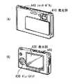
図8は、上記実施の形態の表示装置1が適用されるデジタルカメラの外観を表したものである。このデジタルカメラは、例えば、フラッシュ用の発光部410、表示部420、メニュースイッチ430およびシャッターボタン440を有しており、その表示部420は、上記実施の形態に係る表示装置1により構成されている。
(Application example 2)
FIG. 8 shows the appearance of a digital camera to which the
(適用例3)
図9は、上記実施の形態の表示装置1が適用されるノート型パーソナルコンピュータの外観を表したものである。このノート型パーソナルコンピュータは、例えば、本体510,文字等の入力操作のためのキーボード520および画像を表示する表示部530を有しており、その表示部530は、上記各実施の形態に係る表示装置1により構成されている。
(Application example 3)
FIG. 9 shows an appearance of a notebook personal computer to which the
(適用例4)
図10は、上記実施の形態の表示装置1が適用されるビデオカメラの外観を表したものである。このビデオカメラは、例えば、本体部610,この本体部610の前方側面に設けられた被写体撮影用のレンズ620,撮影時のスタート/ストップスイッチ630および表示部640を有しており、その表示部640は、上記各実施の形態に係る表示装置1により構成されている。
(Application example 4)
FIG. 10 shows the appearance of a video camera to which the
(適用例5)
図11は、上記実施の形態の表示装置1が適用される携帯電話機の外観を表したものである。この携帯電話機は、例えば、上側筐体710と下側筐体720とを連結部(ヒンジ部)730で連結したものであり、ディスプレイ740,サブディスプレイ750,ピクチャーライト760およびカメラ770を有している。そのディスプレイ740またはサブディスプレイ750は、上記各実施の形態に係る表示装置1により構成されている。
(Application example 5)
FIG. 11 shows the appearance of a mobile phone to which the
以上、実施の形態および適用例を挙げて本発明を説明したが、本発明は上記実施の形態等に限定されるものではなく、種々変形が可能である。 While the present invention has been described with the embodiment and application examples, the present invention is not limited to the above-described embodiment and the like, and various modifications can be made.
例えば、上記実施の形態等では、表示装置1がアクティブマトリクス型である場合について説明したが、アクティブマトリクス駆動のための画素回路14の構成は上記実施の形態等で説明したものに限られず、必要に応じて容量素子やトランジスタを画素回路14に追加してもよい。その場合、画素回路14の変更に応じて、上述した信号線駆動回路23、書込線駆動回路24および電源線駆動回路25のほかに、必要な駆動回路を追加してもよい。
For example, in the above-described embodiment, the case where the
また、上記実施の形態等では、信号線駆動回路23、書込線駆動回路24および電源線駆動回路25の駆動をタイミング制御回路22が制御していたが、他の回路がこれらの駆動を制御するようにしてもよい。また、信号線駆動回路23、書込線駆動回路24および電源線駆動回路25の制御は、ハードウェア(回路)で行われていてもよいし、ソフトウェア(プログラム)で行われていてもよい。
In the above embodiment and the like, the
また、上記実施の形態等では、画素回路14が、2Tr1Cの回路構成となっていたが、デュアルゲート型のトランジスタが有機EL素子11に直列に接続された回路構成を含んでいるものであれば、2Tr1Cの回路構成以外の回路構成となっていてもよい。 In the above-described embodiment and the like, the pixel circuit 14 has a 2Tr1C circuit configuration. However, as long as the pixel circuit 14 includes a circuit configuration in which a dual-gate transistor is connected to the organic EL element 11 in series. The circuit configuration may be other than the 2Tr1C circuit configuration.
また、上記実施の形態等では、駆動トランジスタTr1,書き込みトランジスタTr2は、nチャネルMOS型の薄膜トランジスタ(TFT(Thin Film Transistor))により形成されている場合が例示されていたが、pチャネルトランジスタ(例えばpチャネルMOS型のTFT)により形成されていてもよい。ただし、その場合には、トランジスタTr2のソースおよびドレインのうち電源線PSLと未接続の方と保持容量Csの他端とを有機EL素子11のカソードに接続し、有機EL素子11のアノードをGNDなどに接続することが好ましい。 Further, in the above-described embodiment and the like, the case where the drive transistor Tr 1 and the write transistor Tr 2 are formed by n-channel MOS thin film transistors (TFTs) is illustrated, but a p-channel transistor is exemplified. (For example, a p-channel MOS type TFT) may be used. However, in this case, the source and drain of the transistor Tr 2 that are not connected to the power supply line PSL and the other end of the storage capacitor C s are connected to the cathode of the organic EL element 11 and the anode of the organic EL element 11 is connected. Is preferably connected to GND or the like.
1…表示装置、10…表示パネル、11,11R,11G,11B…有機EL素子、12…画素、13…画素回路アレイ部、14…画素回路、20…駆動回路、21…映像信号処理回路、20A,21A…映像信号、20B…同期信号、22…タイミング生成回路、22A…制御信号、23…信号線駆動回路、24…書込線駆動回路、25…電源線駆動回路、Cs…保持容量、DTL…信号線、Id…電流、GND…グラウンド線、G1…トップゲート、G2…バックゲート、PSL…電源線、Tr1…駆動トランジスタ、Tr2…書き込みトランジスタ、Vg…ゲート電圧、Vgs…ゲート−ソース間電圧、Vs…ソース電圧、Vsig…信号電圧、Vb1,Vb2,VccH,VCCL,Voff,Vofs,Von…電圧、Vth…閾値電圧、WSL…書込線。
DESCRIPTION OF
Claims (5)
映像信号に基づいて前記画素回路を駆動する駆動部と
を備え、
前記画素回路は、第1ゲートおよび第2ゲートを含み、かつ前記発光素子に流れる電流を制御するデュアルゲート型の第1トランジスタと、前記映像信号に応じた信号電圧を前記第1ゲートに書き込む第2トランジスタとを有し、
前記駆動部は、前記第1トランジスタのゲート−ソース間電圧の値として採りうる範囲の少なくとも一部が5V以下となるように、前記信号電圧を前記画素回路に印加する
表示装置。 A display unit in which a set of light emitting elements and pixel circuits are two-dimensionally arranged;
A drive unit for driving the pixel circuit based on a video signal,
The pixel circuit includes a first gate and a second gate, and a dual gate type first transistor that controls a current flowing through the light emitting element, and a first voltage that writes a signal voltage corresponding to the video signal to the first gate. Two transistors,
The drive unit applies the signal voltage to the pixel circuit so that at least a part of a range that can be taken as a gate-source voltage value of the first transistor is 5 V or less.
請求項1に記載の表示装置。 The display device according to claim 1, wherein the driving unit applies the signal voltage to the pixel circuit after performing threshold correction of the first transistor.
請求項1または請求項2に記載の表示装置。 The display device according to claim 1, wherein the first gate and the second gate are electrically connected to each other and have the same potential.
前記駆動部を用いて、前記第1トランジスタのゲート−ソース間電圧の値として採りうる範囲の少なくとも一部が5V以下となるように、前記信号電圧を前記画素回路に印加するステップと
を含む表示装置の駆動方法。 A display unit in which a set of light emitting elements and a pixel circuit are two-dimensionally arranged, and a drive unit that drives the pixel circuit based on a video signal, the pixel circuit including a first gate and a second gate; And providing a light-emitting device having a dual-gate first transistor that controls a current flowing through the light-emitting element and a second transistor that writes a signal voltage corresponding to the video signal to the first gate;
Applying the signal voltage to the pixel circuit using the driving unit so that at least a part of a range that can be taken as a gate-source voltage value of the first transistor is 5 V or less. Device driving method.
前記表示装置は、
一組の発光素子および画素回路が2次元配置された表示部と、
映像信号に基づいて前記画素回路を駆動する駆動部と
を備え、
前記画素回路は、第1ゲートおよび第2ゲートを含み、かつ前記発光素子に流れる電流を制御するデュアルゲート型の第1トランジスタと、前記映像信号に応じた信号電圧を前記第1ゲートに書き込む第2トランジスタとを有し、
前記駆動部は、前記第1トランジスタのゲート−ソース間電圧の値として採りうる範囲の少なくとも一部が5V以下となるように、前記信号電圧を前記画素回路に印加する
電子機器。 A display device,
The display device
A display unit in which a set of light emitting elements and pixel circuits are two-dimensionally arranged;
A drive unit for driving the pixel circuit based on a video signal,
The pixel circuit includes a first gate and a second gate, and a dual gate type first transistor that controls a current flowing through the light emitting element, and a first voltage that writes a signal voltage corresponding to the video signal to the first gate. Two transistors,
The electronic device that applies the signal voltage to the pixel circuit so that at least a part of a range that can be taken as a gate-source voltage value of the first transistor is 5 V or less.
Priority Applications (4)
| Application Number | Priority Date | Filing Date | Title |
|---|---|---|---|
| JP2009266735A JP2011112724A (en) | 2009-11-24 | 2009-11-24 | Display device, method of driving the same and electronic equipment |
| US12/926,148 US20110122325A1 (en) | 2009-11-24 | 2010-10-28 | Display device, method of driving the display device, and electronic device |
| KR1020100111342A KR20110058668A (en) | 2009-11-24 | 2010-11-10 | Display device, method of driving the display device, and electronic device |
| CN2010105546574A CN102074187A (en) | 2009-11-24 | 2010-11-17 | Display device, method of driving the display device, and electronic device |
Applications Claiming Priority (1)
| Application Number | Priority Date | Filing Date | Title |
|---|---|---|---|
| JP2009266735A JP2011112724A (en) | 2009-11-24 | 2009-11-24 | Display device, method of driving the same and electronic equipment |
Publications (2)
| Publication Number | Publication Date |
|---|---|
| JP2011112724A true JP2011112724A (en) | 2011-06-09 |
| JP2011112724A5 JP2011112724A5 (en) | 2012-12-06 |
Family
ID=44032708
Family Applications (1)
| Application Number | Title | Priority Date | Filing Date |
|---|---|---|---|
| JP2009266735A Pending JP2011112724A (en) | 2009-11-24 | 2009-11-24 | Display device, method of driving the same and electronic equipment |
Country Status (4)
| Country | Link |
|---|---|
| US (1) | US20110122325A1 (en) |
| JP (1) | JP2011112724A (en) |
| KR (1) | KR20110058668A (en) |
| CN (1) | CN102074187A (en) |
Cited By (3)
| Publication number | Priority date | Publication date | Assignee | Title |
|---|---|---|---|---|
| JP2013137498A (en) * | 2011-07-22 | 2013-07-11 | Semiconductor Energy Lab Co Ltd | Light-emitting device |
| KR20200045598A (en) * | 2018-10-22 | 2020-05-06 | 삼성디스플레이 주식회사 | Transistor substrate and display device including the same |
| JP2021067900A (en) * | 2019-10-28 | 2021-04-30 | 株式会社Joled | Pixel circuit and display device |
Families Citing this family (15)
| Publication number | Priority date | Publication date | Assignee | Title |
|---|---|---|---|---|
| JP2011112723A (en) * | 2009-11-24 | 2011-06-09 | Sony Corp | Display device, method of driving the same and electronic equipment |
| CN103198785B (en) * | 2012-01-04 | 2015-12-02 | 群康科技(深圳)有限公司 | Image element circuit |
| TWI467543B (en) * | 2012-01-04 | 2015-01-01 | Chimei Innolux Corp | Pixel circuits |
| KR101918185B1 (en) * | 2012-03-14 | 2018-11-14 | 삼성디스플레이 주식회사 | Method for detecting array and array detecting apparatus |
| JP6031954B2 (en) * | 2012-11-14 | 2016-11-24 | ソニー株式会社 | LIGHT EMITTING ELEMENT, DISPLAY DEVICE, AND ELECTRONIC DEVICE |
| JP6333382B2 (en) * | 2014-07-23 | 2018-05-30 | シャープ株式会社 | Display device and driving method thereof |
| CN104732927B (en) | 2015-04-09 | 2017-10-03 | 京东方科技集团股份有限公司 | A kind of image element circuit and its driving method and display device |
| CN105741779B (en) * | 2016-03-24 | 2018-03-20 | 北京大学深圳研究生院 | A kind of image element circuit and its driving method based on double-gated transistor |
| US10395588B2 (en) * | 2016-03-31 | 2019-08-27 | Intel Corporation | Micro LED display pixel architecture |
| US9806197B1 (en) | 2016-07-13 | 2017-10-31 | Innolux Corporation | Display device having back gate electrodes |
| EP3367374A1 (en) * | 2017-02-28 | 2018-08-29 | IMEC vzw | An active matrix display and a method for threshold voltage compensation in an active matrix display |
| US10909923B2 (en) * | 2019-05-07 | 2021-02-02 | Samsung Display Co., Ltd. | Pixel circuit and display device including the same |
| CN110767132B (en) * | 2019-10-25 | 2021-02-02 | 深圳市华星光电半导体显示技术有限公司 | TFT (thin film transistor) electrical detection correction method, device and system and display device |
| CN112397031B (en) * | 2020-11-16 | 2022-02-22 | 武汉华星光电半导体显示技术有限公司 | Pixel driving circuit and display panel |
| CN112837651A (en) * | 2021-03-12 | 2021-05-25 | 深圳市华星光电半导体显示技术有限公司 | Pixel driving circuit and display panel |
Citations (4)
| Publication number | Priority date | Publication date | Assignee | Title |
|---|---|---|---|---|
| JP2006091089A (en) * | 2004-09-21 | 2006-04-06 | Casio Comput Co Ltd | Pixel driving circuit and image display device |
| JP2006189871A (en) * | 2004-12-31 | 2006-07-20 | Samsung Electronics Co Ltd | Display device and driving method thereof |
| JP2007310311A (en) * | 2006-05-22 | 2007-11-29 | Sony Corp | Display device and its driving method |
| JP2010224033A (en) * | 2009-03-19 | 2010-10-07 | Toshiba Corp | Display device and driving method of display device |
Family Cites Families (22)
| Publication number | Priority date | Publication date | Assignee | Title |
|---|---|---|---|---|
| US6528950B2 (en) * | 2000-04-06 | 2003-03-04 | Semiconductor Energy Laboratory Co., Ltd. | Electronic device and driving method |
| US6879110B2 (en) * | 2000-07-27 | 2005-04-12 | Semiconductor Energy Laboratory Co., Ltd. | Method of driving display device |
| JP4925528B2 (en) * | 2000-09-29 | 2012-04-25 | 三洋電機株式会社 | Display device |
| JP4789369B2 (en) * | 2001-08-08 | 2011-10-12 | 株式会社半導体エネルギー研究所 | Display device and electronic device |
| JP2004361424A (en) * | 2003-03-19 | 2004-12-24 | Semiconductor Energy Lab Co Ltd | Element substrate, light emitting device and driving method of light emitting device |
| US7071905B1 (en) * | 2003-07-09 | 2006-07-04 | Fan Nong-Qiang | Active matrix display with light emitting diodes |
| US7532187B2 (en) * | 2004-09-28 | 2009-05-12 | Sharp Laboratories Of America, Inc. | Dual-gate transistor display |
| KR101066414B1 (en) * | 2004-05-19 | 2011-09-21 | 재단법인서울대학교산학협력재단 | Driving element and driving method of organic light emitting device, and display panel and display device having the same |
| US7317434B2 (en) * | 2004-12-03 | 2008-01-08 | Dupont Displays, Inc. | Circuits including switches for electronic devices and methods of using the electronic devices |
| TWI264694B (en) * | 2005-05-24 | 2006-10-21 | Au Optronics Corp | Electroluminescent display and driving method thereof |
| CN100353407C (en) * | 2005-11-08 | 2007-12-05 | 友达光电股份有限公司 | Driving method of picture element |
| KR100752380B1 (en) * | 2005-12-20 | 2007-08-27 | 삼성에스디아이 주식회사 | Pixel circuit of Organic Light Emitting Display Device |
| US7545348B2 (en) * | 2006-01-04 | 2009-06-09 | Tpo Displays Corp. | Pixel unit and display and electronic device utilizing the same |
| JP5092304B2 (en) * | 2006-07-31 | 2012-12-05 | ソニー株式会社 | Display device and pixel circuit layout method |
| KR101374507B1 (en) * | 2006-10-31 | 2014-03-26 | 엘지디스플레이 주식회사 | Organic light emitting diode display and driving method thereof |
| JP2008203478A (en) * | 2007-02-20 | 2008-09-04 | Sony Corp | Display device and driving method thereof |
| JP4293262B2 (en) * | 2007-04-09 | 2009-07-08 | ソニー株式会社 | Display device, display device driving method, and electronic apparatus |
| JP4524699B2 (en) * | 2007-10-17 | 2010-08-18 | ソニー株式会社 | Display device |
| JP2009294635A (en) * | 2008-05-08 | 2009-12-17 | Sony Corp | Display device, method for driving display device thereof, and electronic equipment |
| JP2011112723A (en) * | 2009-11-24 | 2011-06-09 | Sony Corp | Display device, method of driving the same and electronic equipment |
| KR101152575B1 (en) * | 2010-05-10 | 2012-06-01 | 삼성모바일디스플레이주식회사 | Pixel circuit of a flat panel display device and method of driving the same |
| US8847942B2 (en) * | 2011-03-29 | 2014-09-30 | Intrigue Technologies, Inc. | Method and circuit for compensating pixel drift in active matrix displays |
-
2009
- 2009-11-24 JP JP2009266735A patent/JP2011112724A/en active Pending
-
2010
- 2010-10-28 US US12/926,148 patent/US20110122325A1/en not_active Abandoned
- 2010-11-10 KR KR1020100111342A patent/KR20110058668A/en not_active Application Discontinuation
- 2010-11-17 CN CN2010105546574A patent/CN102074187A/en active Pending
Patent Citations (4)
| Publication number | Priority date | Publication date | Assignee | Title |
|---|---|---|---|---|
| JP2006091089A (en) * | 2004-09-21 | 2006-04-06 | Casio Comput Co Ltd | Pixel driving circuit and image display device |
| JP2006189871A (en) * | 2004-12-31 | 2006-07-20 | Samsung Electronics Co Ltd | Display device and driving method thereof |
| JP2007310311A (en) * | 2006-05-22 | 2007-11-29 | Sony Corp | Display device and its driving method |
| JP2010224033A (en) * | 2009-03-19 | 2010-10-07 | Toshiba Corp | Display device and driving method of display device |
Cited By (10)
| Publication number | Priority date | Publication date | Assignee | Title |
|---|---|---|---|---|
| JP2013137498A (en) * | 2011-07-22 | 2013-07-11 | Semiconductor Energy Lab Co Ltd | Light-emitting device |
| US10008149B2 (en) | 2011-07-22 | 2018-06-26 | Semiconductor Energy Laboratory Co., Ltd. | Light-emitting device including pixels suppressing variation in luminance |
| US10629122B2 (en) | 2011-07-22 | 2020-04-21 | Semiconductor Energy Laboratory Co., Ltd. | Light-emitting device |
| US11081050B2 (en) | 2011-07-22 | 2021-08-03 | Semiconductor Energy Laboratory Co., Ltd. | Light-emitting device |
| US11741895B2 (en) | 2011-07-22 | 2023-08-29 | Semiconductor Energy Laboratory Co., Ltd. | Light-emitting device |
| KR20200045598A (en) * | 2018-10-22 | 2020-05-06 | 삼성디스플레이 주식회사 | Transistor substrate and display device including the same |
| KR102614573B1 (en) * | 2018-10-22 | 2023-12-18 | 삼성디스플레이 주식회사 | Transistor substrate and display device including the same |
| US11950455B2 (en) | 2018-10-22 | 2024-04-02 | Samsung Display Co., Ltd. | Transistor substrate and display device comprising same |
| JP2021067900A (en) * | 2019-10-28 | 2021-04-30 | 株式会社Joled | Pixel circuit and display device |
| JP7253796B2 (en) | 2019-10-28 | 2023-04-07 | 株式会社Joled | Pixel circuit and display device |
Also Published As
| Publication number | Publication date |
|---|---|
| KR20110058668A (en) | 2011-06-01 |
| CN102074187A (en) | 2011-05-25 |
| US20110122325A1 (en) | 2011-05-26 |
Similar Documents
| Publication | Publication Date | Title |
|---|---|---|
| JP2011112724A (en) | Display device, method of driving the same and electronic equipment | |
| JP2011112723A (en) | Display device, method of driving the same and electronic equipment | |
| KR20240027660A (en) | Display unit, method of manufacturing the same, and electronic apparatus | |
| JP5309455B2 (en) | Display device, driving method thereof, and electronic apparatus | |
| JP2011112722A (en) | Display device, method of driving the same and electronic equipment | |
| JP2010113230A (en) | Pixel circuit, display device and electronic equipment | |
| TWI409755B (en) | Display device and its driving method and electronic machine | |
| JP2009157019A (en) | Display device and electronic equipment | |
| JP2011175103A (en) | Pixel circuit, display device and method for driving the same, and electronic equipment | |
| JP2010243938A (en) | Display and method of driving the same | |
| JP2011022462A (en) | Display device, driving method therefor, and electronics device | |
| JP5577719B2 (en) | Display device, driving method thereof, and electronic apparatus | |
| KR101992491B1 (en) | Pixel circuit, display panel, display unit, and electronic system | |
| JP5321304B2 (en) | Display device, driving method thereof, and electronic apparatus | |
| JP2009047746A (en) | Display device and electronic equipment | |
| JP5282970B2 (en) | Display device, driving method thereof, and electronic apparatus | |
| US20110175868A1 (en) | Display device, method of driving the display device, and electronic unit | |
| JP2012168358A (en) | Display device, driving method of display device, and electronic apparatus | |
| JP5239812B2 (en) | Display device, display device driving method, and electronic apparatus | |
| JP2011022239A (en) | Display device, method of driving the same, and electronic device | |
| JP2011209615A (en) | Display apparatus, driving method for the display apparatus, and electronic equipment | |
| JP2011154200A (en) | Display device, method for driving the same, and electronic equipment | |
| JP2011150079A (en) | Display device, method for driving the same, and electronic equipment | |
| JP2011145394A (en) | Display device, method for driving the same, and electronic equipment | |
| JP2013122481A (en) | Display device, drive method therefor, and electronic device |
Legal Events
| Date | Code | Title | Description |
|---|---|---|---|
| A521 | Request for written amendment filed |
Free format text: JAPANESE INTERMEDIATE CODE: A523 Effective date: 20121023 |
|
| A621 | Written request for application examination |
Free format text: JAPANESE INTERMEDIATE CODE: A621 Effective date: 20121023 |
|
| A131 | Notification of reasons for refusal |
Free format text: JAPANESE INTERMEDIATE CODE: A131 Effective date: 20130227 |
|
| A977 | Report on retrieval |
Free format text: JAPANESE INTERMEDIATE CODE: A971007 Effective date: 20130227 |
|
| A02 | Decision of refusal |
Free format text: JAPANESE INTERMEDIATE CODE: A02 Effective date: 20130702 |