JP4731655B2 - Method for manufacturing semiconductor device - Google Patents
Method for manufacturing semiconductor device Download PDFInfo
- Publication number
- JP4731655B2 JP4731655B2 JP2000033838A JP2000033838A JP4731655B2 JP 4731655 B2 JP4731655 B2 JP 4731655B2 JP 2000033838 A JP2000033838 A JP 2000033838A JP 2000033838 A JP2000033838 A JP 2000033838A JP 4731655 B2 JP4731655 B2 JP 4731655B2
- Authority
- JP
- Japan
- Prior art keywords
- film
- tft
- semiconductor film
- region
- driver circuit
- Prior art date
- Legal status (The legal status is an assumption and is not a legal conclusion. Google has not performed a legal analysis and makes no representation as to the accuracy of the status listed.)
- Expired - Fee Related
Links
Images


Landscapes
- Liquid Crystal (AREA)
- Recrystallisation Techniques (AREA)
- Devices For Indicating Variable Information By Combining Individual Elements (AREA)
- Physical Deposition Of Substances That Are Components Of Semiconductor Devices (AREA)
- Thin Film Transistor (AREA)
Description
【0001】
【発明の属する技術分野】
本願発明は薄膜トランジスタ(以下、TFTという)で構成された回路を有する半導体装置に関する。例えば、液晶表示パネルに代表される電気光学装置およびその様な電気光学装置を部品として搭載した電子機器の構成に関する。
【0002】
なお、本明細書中において半導体装置とは、半導体特性を利用することで機能しうる装置全般を指し、電気光学装置、半導体回路および電子機器は全て半導体装置である。
【0003】
【従来の技術】
近年、絶縁表面を有する基板上に形成された半導体薄膜(厚さ数〜数百nm程度)を用いて薄膜トランジスタ(TFT)を構成する技術が注目されている。薄膜トランジスタはICや電気光学装置のような電子デバイスに広く応用され、特に画像表示装置のスイッチング素子として開発が急がれている。
【0004】
例えば、液晶表示装置においてはマトリクス状に配列された画素を個々に制御する画素部、画素部を制御するドライバー回路、さらに外部からのデータ信号を処理するロジック回路(プロセッサ回路やメモリ回路など)等のあらゆる電気回路にTFTを応用する試みがなされている。
【0005】
そして、これらの回路(画素部、ドライバー回路等)を一枚の基板上に集積化した構成(システム・オン・パネル)が知られている。画素部において、画素はドライバー回路から送られた情報を保持する役割を果たしており、画素に接続されているTFTのオフ電流が十分に小さくないと、その情報を保持することができず、良好な表示を得ることはできない。
【0006】
一方、ドライバー回路において、TFTは高移動度が要求されており、移動度が高ければ高いほど、回路構造を簡単にでき、且つ、表示装置を高速に動作させることができる。
【0007】
以上のように、ドライバー回路に配置されるTFTと画素部に配置されるTFTでは、要求される特性が異なる。即ち、画素部に配置されるTFTはそれほど高移動度は要求されないが、オフ電流が小さく、且つ、画素部でその値が均一であることが要求される。逆に、周辺に配置されるドライバー回路のTFTはオフ電流よりも移動度が優先され、高移動度が要求される。
【0008】
しかし、従来の作製方法を用いて、同一基板上に移動度を優先するTFTと、オフ電流の小さいTFTとを信頼性を損なうことなく生産性よく作製することは、困難であった。
【0009】
【発明が解決しようとする課題】
以上のように、ロジック回路を内蔵したシステム・オン・パネルを実現するためには、従来にない全く新しい構成が求められている。
【0010】
本願発明は、その様な要求に答えるものであり、AM−LCDに代表される電気光学装置の各回路を機能に応じて適切な構造のTFTでもって形成し、高い信頼性を有する電気光学装置を提供することを課題とする。
【0011】
【課題を解決するための手段】
本明細書で開示する発明の構成は、
同一基板上に形成されたドライバー回路と画素部とを有する半導体装置において、
前記ドライバー回路に含まれる少なくとも一つのTFTのチャネル形成領域は、結晶質半導体膜でなり、
前記画素部に含まれるTFTのチャネル形成領域は、非晶質半導体膜でなることを特徴とする半導体装置である。
【0012】
また、上記構成において、前記ドライバー回路に含まれる少なくとも一つのTFTのチャネル形成領域はレーザーもしくはそれと同様な強光による照射工程を経て形成されたことを特徴としている。
【0013】
また、上記構成において、前記ドライバー回路に含まれる少なくとも一つのTFT及び前記画素部に含まれるTFTのチャネル形成領域は、スパッタ法により形成された半導体膜からなることを特徴としている。
【0014】
また、上記構成において、前記ドライバー回路に含まれる少なくとも一つのTFT及び画素部に含まれるTFTのゲート絶縁膜は、スパッタ法により形成された絶縁膜からなることを特徴としている。
【0015】
また、上記構成において、前記結晶質半導体膜はポリシリコンであり、前記非晶質半導体膜はアモルファスシリコンであることを特徴としている。
【0016】
また、上記各構成において、半導体装置は、アクティブマトリクス型の表示装置であり、例えばEL表示装置、液晶表示装置であることを特徴としている。
【0017】
また、上記構造を実現するための発明の構成は、
同一基板上にドライバー回路と画素部とを有する半導体装置の作製方法であって、
絶縁表面上に非晶質半導体膜を形成する第1工程と、
前記非晶質半導体膜に対して選択的にレーザーもしくはそれと同様な強光を照射して前記非晶質半導体膜の一部を結晶質半導体膜とする第2工程と、
前記結晶質半導体膜をパターニングしてドライバー回路の半導体層を形成し、前記非晶質半導体膜をパターニングして画素部の半導体層を形成する第3工程と、
前記半導体層上に絶縁膜を形成する第4工程と、
前記絶縁膜上にゲート電極を形成する第5工程と、
を有することを特徴とする半導体装置の作製方法である。
【0018】
また、上記構成において、前記第4工程はスパッタ法により行われることを特徴としている。
【0019】
また、他の発明の構成は、
同一基板上にドライバー回路と画素部とを有する半導体装置の作製方法であって、
絶縁表面上に非晶質半導体膜を形成する第1工程と、
前記非晶質半導体膜上に絶縁膜を形成する第2工程と、
前記絶縁膜を介し、前記非晶質半導体膜に対して選択的にレーザーもしくはそれと同様な強光を照射して前記非晶質半導体膜の一部を結晶質半導体膜とする第3工程と、
前記結晶質半導体膜をパターニングしてドライバー回路の半導体層を形成し、前記非晶質半導体膜をパターニングして画素部の半導体層を形成する第4工程と、
前記絶縁膜上にゲート電極を形成する第5工程と、
を有することを特徴とする半導体装置の作製方法である。
【0020】
また、作製方法に関する上記構成において、前記第2工程はスパッタ法により行われることを特徴としている。
【0021】
また、作製方法に関する上記各構成において、前記第1工程はスパッタ法により行われることを特徴としている。
【0022】
また、他の発明の構成は、
同一基板上にドライバー回路と画素部とを有する半導体装置の作製方法であって、
絶縁表面上にゲート電極を形成する第1工程と、
前記ゲート電極上に絶縁膜を形成する第2工程と、
前記絶縁膜上に非晶質半導体膜を形成する第3工程と、
前記非晶質半導体膜に対して選択的にレーザーもしくはそれと同様な強光を照射して前記非晶質半導体膜の一部を結晶質半導体膜とする第4工程と、
前記結晶質半導体膜をパターニングしてドライバー回路の半導体層を形成し、前記非晶質半導体膜をパターニングして画素部の半導体層を形成する第5工程と、
を有することを特徴とする半導体装置の作製方法である。
【0023】
また、作製方法に関する上記各構成において、前記第5工程の後、
ソース領域またはドレイン領域となる領域に対して15族または13族に属する元素を選択的に添加する第6工程と、
半導体層に添加された前記13族及び15族に属する元素を活性化させる処理を行う第7工程と、
を有することを特徴としている。
【0024】
また、作製方法に関する上記各構成において、前記半導体装置は液晶表示装置であることを特徴としている。
【0025】
また、作製方法に関する上記構成において、活性化させる処理を行う第7工程の後に、
前記活性層上方に層間絶縁膜を形成する第8工程と、
前記層間絶縁膜上に画素電極を形成する第9工程と、
前記画素電極の上にEL層を形成する第10工程と、
前記EL層の上に陰極または陽極を形成する第11工程とを有することを特徴としている。
【0026】
また、作製方法に関する上記各構成において、前記半導体装置はEL表示装置であることを特徴としている。
【0027】
【発明の実施の形態】
本願発明の実施形態について、以下に説明する。本発明においては、同一基板上に形成されたAM−LCDやEL表示装置に代表される電気光学装置の各回路のTFTの活性層として非晶質半導体膜または結晶質半導体膜を機能に応じて用いることを特徴とする。例えば、AM−LCDやEL表示装置に代表される電気光学装置において、画素部に配置されるTFTの活性層として非晶質半導体膜(アモルファスシリコン膜等)を用い、ドライバー回路やロジック回路などの様に、高速動作性能を求められる電気回路に配置されるTFTの活性層として結晶質半導体膜(ポリシリコン膜、多結晶シリコン膜等)を利用することを特徴とする。
【0028】
上記構成を実現するためには、同一基板上に非晶質半導体膜を選択的に結晶化して結晶質半導体膜を形成する必要があり、本願発明は、その形成方法にも特徴がある。
【0029】
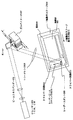
その本願発明の形成方法の一例を図1を用いて説明する。図1は、基板に形成されたドライバー回路103の非晶質半導体膜のみにエキシマレーザー等のパルス発振レーザーを照射する場合の例を示した簡略図である。
【0030】
図1において、101は耐熱性を有する基板であり、ガラス基板、石英基板、シリコン基板、セラミックス基板、金属基板(代表的にはステンレス基板)を用いれば良い。どの基板を用いる場合においても、必要に応じて下地膜(好ましくは珪素を主成分とする絶縁膜)を設けても構わない。なお、図示しないが基板101上には、スパッタ法を用いて成膜された非晶質半導体膜が設けられている。従って、この段階で実際は明確な境界は目視できないが、都合上、後に形成される画素部102とドライバー回路103とを示した。
【0031】
エキシマレーザー光源105から出射されたレーザー光は、光学系(ビームホモジナイザー106、ミラー107等)により、ビーム形状及びエネルギー密度等を調節され、レーザースポット108を形成する。そして、基板101が固定されたX−Yステージ104をX方向またはY方向に移動させることによって、ドライバー回路103の非晶質半導体膜のみにレーザースポット108をレーザースポットスキャン方向109に照射する。ただし、非晶質半導体膜の膜厚等を考慮に入れて、レーザー光の条件(照射強度、パルス幅、繰り返し周波数、照射時間、基板温度、ステージの移動速度、オーバーラップ率等)を実施者が適宜決定する。また、ここでは、レーザー光がもれて画素部102に照射された場合、TFTの特性にバラツキが生じるため、レーザー光がもれないよう光学系を配置することが重要である。加えて、ドライバー回路と画素部の間隔Xも適宜設定することが必要である。
【0032】
図1に示したレーザー照射方法を用いれば、ドライバー回路103のみにレーザー光を照射することが可能となり選択的に非晶質珪素膜を結晶化させることができる。
【0033】
また、レーザー光としては、エキシマレーザー等のパルス発振レーザー以外に、アルゴンレーザー等の連続発振レーザーや連続発光エキシマレーザー等を用いることも可能である。
【0034】
また、非晶質半導体膜上に絶縁膜を形成した後、上記レーザー光の照射を行う工程としてもよい。
【0035】
図6は、アルゴンレーザー等の連続発振レーザーを照射する場合の例を示している。図6において、601は基板、606はビームエキスパンダー、607はガルバノメータ、604は一軸動作ステージである。また、図示しないが基板601上には、スパッタ法を用いた非晶質半導体膜が設けられている。
【0036】
アルゴンレーザー光源605から出射されたレーザー光は、光学系(ビームエキスパンダー606、ガルバノメータ607、f−シータレンズ608等)により、ビーム形状及びエネルギー密度等を調節され、レーザースポット609を形成する。そして、ガルバノメータを振動させることによりレーザースポット609をレーザースポットスキャン方向610と平行な方向に振動させると同時に、基板601が固定された一軸動作ステージ604を一方向(一軸動作ステージの動作方向611)にステップ移動(ステップの間隔はスポット径程度とする)させることによって、ドライバー回路603の非晶質半導体膜のみを結晶化する。図1に示したレーザー照射方法と同様に、レーザー光がもれて画素部602に照射されないよう光学系を配置することが重要である。
【0037】
図6に示したレーザー照射方法を用いれば、図1に示したレーザー照射方法と同様にドライバー回路のみにレーザー光を照射することが可能となり選択的に非晶質珪素膜を結晶化させることができる。
【0038】
また、図1及び図6の構成に加えて、レーザー光がもれて画素部に照射されないよう通常のフォトリソグラフィー工程を用いたレジストマスクを基板に形成してもよいし、フォトマスクを用いてもよい。
【0039】
また、図1及び図6では、スポットレーザーを形成する例を示したが、特に限定されず、マスクを用いて選択的に線状レーザー光を照射する構成としてもよい。あるいはソプラに代表される大面積スポットレーザーをドライバー回路サイズに加工し、ドライバー回路の非晶質半導体領域を同時に結晶化させる工程を用いても良い。
【0040】
上記本願発明のレーザー光の照射方法を利用して同一基板上にドライバー回路と画素部とを一体形成したAM−LCDの断面図を図4(C)に示している。なお、ここではドライバー回路を構成する基本回路としてCMOS回路を示し、画素部のTFTとしてはダブルゲート構造のTFTを示している。勿論、ダブルゲート構造に限らずトリプルゲート構造やシングルゲート構造などとしても良い。
【0041】
202は下地膜として設けた酸化珪素膜であり、その上にドライバー回路のTFTの活性層、画素部のTFTの活性層および保持容量の下部電極となる半導体層が形成される。なお、本明細書中において「電極」とは、「配線」の一部であり、他の配線との電気的接続を行う箇所、または半導体層と交差する箇所を指す。従って、説明の便宜上、「配線」と「電極」とを使い分けるが、「配線」という文言に「電極」は常に含められているものとする。
【0042】
図4(C)において、ドライバー回路のTFTの活性層は、Nチャネル型TFT(以下、NTFTという)のソース領域221、ドレイン領域220、LDD(ライトドープトドレイン)領域228およびチャネル形成領域209、並びにPチャネル型TFT(以下、PTFTという)のソース領域215、ドレイン領域216およびチャネル形成領域217で形成される。
【0043】
また、画素部のTFT(ここではNTFTを用いる。)の活性層は、ソース領域222、ドレイン領域224、LDD領域229およびチャネル形成領域212で形成される。さらに、ドレイン領域224から延長された半導体層を保持容量の下部電極226として用いる。
【0044】
なお、図1では下部電極226が画素部のTFTのドレイン領域224と直接的に接続されているが、間接的に接続させて下部電極226とドレイン領域224とが電気的に接続するような構造としても良い。
【0045】
この下部電極226には、半導体層に対して15族に属する元素が添加されている。即ち、保持容量の上部配線206fに電圧を印加しなくても、そのまま電極として用いることが可能となっているため、AM−LCDの消費電力の低減に有効である。
【0046】
また、画素部のTFTのチャネル形成領域212はアモルファス状態の半導体膜とであり、ドライバー回路のTFTのチャネル形成領域209、217は、結晶性を有する結晶質半導体膜である点も本願発明の特徴の一つである。
【0047】
また、各TFTのチャネル形成領域209、212、217は、スパッタ法を用いて形成された半導体膜であり、膜中の水素濃度が低い点も本願発明の一つである。スパッタ法により成膜した半導体膜はプラズマCVD法により成膜した半導体膜と比較して水素濃度が一桁以上低く、脱水素処理をしなくとも成膜後、連続的にレーザー結晶化できる。一方、プラズマCVD法を用いたプロセスでは、爆発の危険性が高く、作業環境の安全性の観点からは不利であった。本願発明においては、安全性及び生産性を優先するため、非晶質半導体膜(アモルファスシリコン膜等)や、絶縁膜や、導電層等の薄膜形成をスパッタ法で形成することを特徴とする。さらに好ましくは、大気からの汚染防止のため、可能な限り各膜を連続成膜する。
【0048】
また、ここでは、各TFTのゲート絶縁膜205を同じ膜厚の同一絶縁膜としたが、特に限定されない。例えば、回路特性に応じて同一基板上に異なるゲート絶縁膜を有するTFTが少なくとも二種類以上存在する構成としてもよい。なお、半導体膜とゲート絶縁膜をスパッタ法を用いて連続的に形成すると良好な界面が得られるため好ましい。
【0049】
次に、ゲート絶縁膜205の上にはドライバー回路のTFTのゲート配線206d、と、画素部のTFTのゲート配線206eが形成される。また、同時に保持容量の下部電極226上にはゲート絶縁膜205を介して保持容量の上部電極206fが形成される。
【0050】
本発明の配線材料としては、代表的には、導電性を有する珪素膜(例えばリンドープシリコン膜、ボロンドープシリコン膜等)や金属膜(例えばタングステン膜、タンタル膜、モリブデン膜、チタン膜、アルミニウム膜、銅膜等)でも良いし、前記金属膜をシリサイド化したシリサイド膜、窒化した金属膜(窒化タンタル膜、窒化タングステン膜、窒化チタン膜等)でも良い。また、これらを自由に組み合わせて積層しても良い。
【0051】
また、前記金属膜を用いる場合には、金属膜の酸化を防止するために珪素膜との積層構造とすることが望ましい。また、酸化防止という意味では、金属膜を窒化珪素膜で覆った構造が有効である。
【0052】
次に、230は第1層間絶縁膜であり、珪素を含む絶縁膜(単層または積層)で形成される。珪素を含む絶縁膜としては、酸化珪素膜、窒化珪素膜、酸化窒化珪素膜(酸素よりも窒素の含有量の方が多い)、窒化酸化珪素膜(窒素よりも酸素の含有量の方が多い)を用いることができる。
【0053】
そして、第1層間絶縁膜230にはコンタクトホールが設けられ、ドライバー回路のTFTのソース配線231、233、ドレイン配線232、および画素部のTFTのソース配線234、ドレイン配線235が形成される。その上にはパッシベーション膜236、第2層間絶縁膜237が形成され、コンタクトホールを設けた後、画素電極238が形成される。
【0054】
なお、図4(C)ではブラックマスク(遮光膜)を形成していないが、特に限定されず、必要に応じて形成すれば良い。例えば、対向基板に遮光膜を設ける構成としても良いし、各TFTの下または上にゲート配線と同様の材料を用いた遮光膜を設けるような構造としても良い。
【0055】
第2層間絶縁膜237としては、比誘電率の小さい樹脂膜が好ましい。樹脂膜としては、ポリイミド膜、アクリル膜、ポリアミド膜、BCB(ベンゾシクロブテン)膜などを用いることができる。
【0056】
また、画素電極238としては、透過型AM−LCDを作製するのであればITO膜に代表される透明導電膜を、反射型AM−LCDを作製するのであればアルミニウム膜に代表される反射率の高い金属膜を用いれば良い。
【0057】
なお、図4では画素電極238がドレイン電極235を介して画素部のTFTのドレイン領域224と電気的に接続されているが、画素電極238とドレイン領域224とが直接的に接続するような構造としても良い。
【0058】
以上のような構造でなるAM−LCDは、機能に応じて適切な構造のTFTでもって各回路が形成されるため、駆動能力、信頼性、及び生産性が高い点に特徴がある。
【0059】
以上の構成でなる本願発明について、以下に示す実施例でもってさらに詳細な説明を行うこととする。
【0060】
【実施例】
[実施例1]
本実施例では、「発明の実施の形態」で説明した図4(C)の構造を実現するための作製工程について説明する。説明には図2〜4を用いる。
【0061】
まず、基板としてガラス基板201を用意し、その上に200nm厚の酸化珪素膜(下地膜とも呼ぶ)202と厚さ55nmの非晶質珪素膜203aとを大気解放しないまま連続的にスパッタ法にて成膜した。(図2(A))こうすることで非晶質珪素膜203aの下表面に大気中に含まれるボロン等の不純物が吸着することを防ぐことができる。
【0062】
なお、本実施例では非晶質半導体膜として、非晶質珪素(アモルファスシリコン)膜を用いたが、他の半導体膜であっても構わない。非晶質シリコンゲルマニウム膜でも良い。また、下地膜及び半導体膜の形成手段としては、PCVD法、LPCVD法またはスパッタ法等を用いることができる。中でも安全性及び生産性の面で優れているためスパッタ法が望ましい。本実施例で用いたスパッタ装置は、チャンバーと、チャンバー内を真空にする排気系と、スパッタ用のガスをチャンバー内に導入するガス導入系と、ターゲットやRF電極等からなる電極系と、電極系に接続されたスパッタリング電源とを備えている。本実施例では、スパッタ用のガスとしてアルゴン(Ar)、ターゲットとしてシリコンターゲットを用いた。
【0063】
本実施例においては、画素部のTFTのチャネル形成領域は非晶質珪素膜(非晶質珪素膜からなるNTFTの電界効果移動度μFEは1.0cm2/Vsより小さい)で構成することとなるので、チャネル長、非晶質珪素膜の膜厚を適宜設定する必要がある。
【0064】
次に、非晶質珪素膜204aの結晶化を行う。結晶化の手段としては、レーザー結晶化、触媒元素を用いた熱結晶化等の公知の技術を用いる。本実施例では、図1に簡略に示したレーザー照射方法を用いてレーザー結晶化を行った。エキシマレーザー光源105から出射されたレーザー光は、光学系(ビームホモジナイザー106、ミラー107等)により、ビーム形状及びエネルギー密度等を調節され、レーザースポット108を形成した。そして、基板101が固定されたX−Yステージ104をX方向またはY方向に移動させることによって、ドライバー回路103の非晶質半導体膜のみにレーザースポット108をレーザースポットスキャン方向109に照射した。こうしてドライバー回路のみにレーザー照射を行って選択的に結晶化させ、結晶質珪素(ポリシリコン)膜からなる領域204aを形成した。(図2(B))
【0065】
本実施例においては、ドライバー回路のTFTのチャネル形成領域は結晶質珪素膜(結晶質珪素膜からなるNTFTの電界効果移動度μFEは1.0cm2/Vs以上)で構成することとなるので、適宜、最適なチャネル長、十分にレーザー結晶化可能な非晶質珪素膜の膜厚とする必要がある。以上のことを考慮に入れると、チャネル長は3〜10μmであればよく、非晶質珪素膜の膜厚は、10〜200nm、好ましくは30〜70nmであればよい。
【0066】
そして、形成された結晶質珪素(ポリシリコン)膜をパターニングして、ドライバー回路のTFTの半導体層204bを形成し、非晶質珪素(アモルファスシリコン)膜をパターニングして画素部のTFTの半導体層203bを形成した。(図2(C))
【0067】
なお、ドライバー回路のTFTおよび画素部のTFTの半導体層203b、204bを形成する前後に、結晶質珪素膜に対してTFTのしきい値電圧を制御するための不純物元素(リンまたはボロン)を添加しても良い。この工程はNTFTまたはPTFTのみに行っても良いし、双方に行っても良い。
【0068】
次に、スパッタ法またはプラズマCVD法によりゲート絶縁膜205を形成し、スパッタ法により第1の導電膜206a、第2の導電膜207aを積層形成する。(図2(D))
【0069】
このゲート絶縁膜205は、TFTのゲート絶縁膜として機能することになる絶縁膜であり、膜厚は50〜200nmとする。本実施例では、シリコン酸化物をターゲットとして用いたスパッタ法により100nm厚の酸化珪素膜を形成した。また、酸化珪素膜のみでなく酸化珪素膜の上に窒化珪素膜を設けた積層構造とすることもできるし、酸化珪素膜に窒素を添加した酸化窒化珪素膜を用いても構わない。
【0070】
なお、本実施例では非晶質珪素膜のレーザー結晶化を行った後、パターニングを行いゲート絶縁膜を形成した例を示したが、特に工程順序は限定されず、非晶質珪素膜とゲート絶縁膜をスパッタ法にて連続成膜した後、レーザー結晶化を行いパターニングを施す工程としてもよい。スパッタ法にて連続成膜した場合、良好な界面特性が得られる。
【0071】
また、第1の導電膜206aは、Ta、Ti、Mo、Wから選ばれた元素を主成分とする導電材料を用いる。第1の導電膜206aの厚さは5〜50nm、好ましくは10〜25nmで形成すれば良い。一方、第2の導電膜207aは、Al、Cu、Siを主成分とする導電材料を用いる。第2の導電膜207aは100〜1000nm、好ましくは200〜400nmで形成すれば良い。第2の導電膜207aは、ゲート配線またはゲートバスラインの配線抵抗を下げるために設けられている。
【0072】
次いで、パターニングによって第2の導電膜207aの不要な部分を除去して、配線部にゲートバスラインの一部となる電極207bを形成した後、レジストマスク208a〜dを形成する。レジストマスク208aはPTFTを覆い、レジストマスク208bはドライバー回路のNTFTのチャネル形成領域を覆うようにして形成する。また、レジストマスク208cは電極207bを覆い、レジストマスク208dは画素部のチャネル形成領域を覆うようにして形成する。その後、レジストマスク208a〜dをマスクとしてn型を付与する不純物元素の添加を行い、不純物領域210、211を形成した。(図3(A))
【0073】
本実施例ではn型を付与する不純物元素としてリンを用い、フォスフィン(PH3)を用いたイオンドープ法で行った。この工程ではゲート絶縁膜205と第1の導電膜206aを通してその下の半導体層203b、204bにリンを添加するために、加速電圧は80keVとして、高めに設定した。半導体層203b、204bに添加されるリンの濃度は、1×10¹⁶〜1×10¹⁹atoms/cm3の範囲にするのが好ましく、ここでは1×1018atoms/cm3とした。そして、半導体層にリンが添加された領域210、211が形成された。ここで形成されたリンが添加された領域の一部は、LDD領域として機能する。また、マスクで覆われてリンが添加されなかった領域(結晶質珪素膜からなる領域209、非晶質珪素膜からなる領域212)の一部は、チャネル形成領域として機能する。
【0074】
なお、リンの添加工程は、質量分離を行うイオンインプランテーション法を用いても良いし、質量分離を行わないプラズマドーピング法を用いても良い。また、加速電圧やドーズ量の条件等は実施者が最適値を設定すれば良い。
【0075】
次いで、レジストマスク208a〜dを除去した後、必要があれば活性化処理を行う。そして、第3の導電膜213aをスパッタ法により成膜形成した。(図3(B))第3の導電膜213aは、Ta、Ti、Mo、Wから選ばれた元素を主成分とする導電材料を用いる。また、第3の導電膜213aの厚さは100〜1000nm、好ましくは200〜500nmとした。
【0076】
次いで、レジストマスク214a〜dを新たに形成してパターニングを行いPTFTのゲート電極206b、213bの形成、及び配線206c、213cの形成を行った後、マスク214a〜dをそのまま用いてp型を付与する不純物元素を添加してPTFTのソース領域、ドレイン領域を形成する。(図3(C))ここではボロンをその不純物元素として、ジボラン(B2H6)を用いてイオンドープ法で添加した。ここでも加速電圧を80keVとして、2×10²⁰atoms/cm3の濃度にボロンを添加した。
【0077】
次いで、レジストマスク214a〜dを除去して、新たにレジストマスク218a〜eを形成した後、レジストマスク218a〜eをマスクとしてエッチングを行いNTFTのゲート配線206d、213d、画素部のTFTのゲート配線206e、213e、保持容量の上部配線206f、213fを形成する。(図3(D))
【0078】
次いで、レジストマスク218a〜eを除去し、新たにレジストマスク219を形成した後、NTFTのソース領域、ドレイン領域にn型を付与する不純物元素を添加して不純物領域220〜225を形成する。(図4(A))ここでは、フォスフィン(PH3)を用いたイオンドープ法で行った。不純物領域220〜225に添加されたリンの濃度は、先のn型を付与する不純物元素を添加する工程と比較して高濃度であり、1×10¹⁹〜1×10²¹atoms/cm3とするのが好ましく、ここでは1×1020atoms/cm3とした。
【0079】
その後、レジストマスク219を除去した後、50nmの厚さの窒化珪素膜からなる保護膜227を形成して図4(B)の状態が得られる。
【0080】
次いで、添加されたn型またはp型を付与する不純物元素を活性化するための活性化処理を行う。この工程は、電気加熱炉を用いた熱アニール法や、前述のエキシマレーザーを用いたレーザーアニール法や、ハロゲンランプを用いたラピットサーマルアニール法(RTA法)で行えば良い。加熱処理する場合は、300〜700℃、好ましくは350〜550℃、本実施例では窒素雰囲気において450℃、2時間の熱処理を行った。
【0081】
次いで、第1の層間絶縁膜230を形成した後、コンタクトホールを形成し、ソース電極及びドレイン電極231〜235等を公知の技術により形成する。
【0082】
その後、パッシベーション膜236を形成する。パッシベーション膜236としては、窒化珪素膜、酸化窒化珪素膜、窒化酸化珪素膜、またはこれらの絶縁膜と酸化珪素膜との積層膜を用いることができる。本実施例では300nm厚の窒化珪素膜をパッシベーション膜として用いた。
【0083】
なお、本実施例では窒化珪素膜を形成する前処理として、アンモニアガスを用いたプラズマ処理を行い、そのままパッシベーション膜236を形成する。この前処理によりプラズマで活性化した(励起した)水素がパッシベーション膜236によって閉じこめられるため、TFTの活性層(半導体層)の水素終端を促進させることができる。
【0084】
さらに、水素を含むガスに加えて亜酸化窒素ガスを加えると、発生した水分によって被処理体の表面が洗浄され、特に大気中に含まれるボロン等による汚染を効果的に防ぐことができる。
【0085】
パッシベーション膜236を形成したら、第2層間絶縁膜237として1μm厚のアクリル膜を形成した後、パターニングしてコンタクトホールを形成し、ITO膜でなる画素電極238を形成した。こうして図4(C)に示すような構造のAM−LCDが完成する。
【0086】
以上の工程で、ドライバー回路のNTFTにはチャネル形成領域209、不純物領域220、221、LDD領域228が形成された。不純物領域220はソース領域として、不純物領域221はドレイン領域となった。また、画素部のNTFTには、チャネル形成領域212、不純物領域222〜225、LDD領域229が形成された。ここで、LDD領域228、229は、ゲート電極と重なる領域(GOLD領域)と、ゲート電極と重ならない領域(LDD領域)がそれぞれ形成された。
【0087】
一方、pチャネル型TFTは、チャネル形成領域217、不純物領域215、216が形成された。そして、不純物領域215はソース領域として、不純物領域216はドレイン領域となった。
【0088】
このように本願発明は、同一基板上に非晶質珪素膜からなるチャネル形成領域212を有する画素部のTFTと、結晶質珪素膜からなるチャネル形成領域209、217を有するドライバー回路のTFTとを形成する点に特徴がある。このような構成により均一性の高い画素部のTFTと移動度の高いドライバー回路のTFTを同一基板上に形成することが可能となる。
【0089】
図5(A)はアクティブマトリクス型液晶表示装置の回路構成の一例を示す。本実施例のアクティブマトリクス型液晶表示装置は、ソース信号線側ドライバー回路301、ゲート信号線側ドライバー回路(A)307、ゲート信号線側ドライバー回路(B)311、プリチャージ回路312、画素部306を有している。
【0090】
ソース信号線側ドライバー回路301は、シフトレジスタ回路302、レベルシフタ回路303、バッファ回路304、サンプリング回路305を備えている。
【0091】
また、ゲート信号線側ドライバー回路(A)307は、シフトレジスタ回路308、レベルシフタ回路309、バッファ回路310を備えている。ゲート信号線側ドライバー回路(B)311も同様な構成である。
【0092】
本発明は、画素部以外の回路をドライバー回路としてその領域の半導体層を結晶化しているが、特に限定されない。即ち、ドライバー回路のうち、高移動度よりも信頼性が要求される回路は結晶化しなくともよい。例えば、ドライバー回路の中でも、バッファ回路等は画素部のNTFTと同様にチャネル形成領域をアモルファス状態の半導体層で構成してもよい。
【0093】
また、本発明は、NTFTの駆動電圧を考慮して、LDD領域の長さを同一基板上で異ならしめることが容易であり、それぞれの回路を構成するTFTに対して、最適な形状を同一工程で作り込むこともできる。
【0094】
また、図5(B)は画素部の上面図を示し、TFT部分のA−A' 断面構造と配線部のB−B' 断面構造は、図4(C)と対応しているため、一部は同一の符号で示した。図5(B)中、401は半導体層、402はゲート電極、403aは容量線を示している。本実施例において、ゲート電極とゲート配線403bは、第1の導電層と第3の導電層とから形成され、ゲートバスラインは、第1の導電層と第2の導電層と第3の導電層とから形成されたクラッド構造を有している。
【0095】
また、図10(A)は、ドライバー回路を構成する一部となるCMOS回路の上面図を示し、図4(C)と対応している。また、本実施例ではNTFTとPTFTの活性層が直接接し、ドレイン電極を共有しているが、特にこの構造に限定されず、図10(B)に示すような構造(活性層が完全に分離)としてもよい。
【0096】
〔実施例2〕
本実施例では、実施例1と異なるレーザーを用いて非晶質半導体膜を選択的に結晶化する例を図6を用いて以下に説明する。本実施例は、レーザー結晶化の工程以外は実施例1と同一であるため、異なる点にのみ着目して説明を行う。
【0097】
まず、実施例1の作製工程に従って、基板上に酸化珪素膜(下地膜)と非晶質珪素膜を連続成膜する。本実施例では基板として石英基板を用いた。また、アルゴンレーザーの吸収係数の関係により非晶質珪素膜の膜厚は100nm以上とすることが好ましい。
【0098】
次いで、レーザー結晶化の際、図6に示した照射方法を用いて選択的に結晶化を行う。アルゴンレーザー光源605から出射されたレーザー光は、光学系(ビームエキスパンダー606、ガルバノメータ607、f−シータレンズ608等)により、ビーム形状及びエネルギー密度等を調節され、レーザースポット609を形成した。そして、ガルバノメータを振動させることによりレーザースポット609をレーザースポットスキャン方向610と平行な方向に振動させると同時に、基板601が固定された一軸動作ステージ604を一方向(一軸動作ステージの動作方向611)にステップ移動(ステップの間隔はスポット径程度とする)させることによって、ドライバー回路のみにレーザー照射を行って選択的に結晶化させ、結晶質珪素(ポリシリコン)膜からなる領域を形成した。
【0099】
以降の工程は実施例1に従えば図4(C)で示した状態を得ることができる。
【0100】
〔実施例3〕
実施例1、2に示した作製工程では、図1または図2に示したレーザー照射方法を用いて選択的にドライバー回路のみに照射しているが、通常のレジストマスクを用いてレーザー光を選択的に照射することも可能である。
【0101】
この場合、従来のレーザー照射装置をそのまま用いることができる。従って、装置を変更することなく容易に行えるため有効な技術と言える。
【0102】
また、本実施例の構成は実施例1〜2のいずれの実施例とも自由に組み合わせることが可能である。
【0103】
〔実施例4〕
本実施例では、実施例1と異なる工程でAM−LCDを作製する場合の例について図7〜9を用いて説明する。実施例1ではトップゲート型TFTの例を示したが本実施例ではボトムゲート型TFTの例を示す。
【0104】
まず、ガラス基板701上に積層構造(簡略化のため図示しない)のゲート電極702を形成する。本実施例ではスパッタ法を用いて窒化タンタル膜とタンタル膜を積層形成し、公知のパターニングによりゲート配線(ゲート電極含む)702a〜c及び容量配線702dを形成した。
【0105】
次いで、ゲート絶縁膜、非晶質半導体膜を順次大気開放せずに積層形成した。本実施例では、窒化珪素膜と酸化珪素膜の積層をスパッタ法にて形成し、積層構造のゲート絶縁膜とした。(図7(A))次いで、大気開放せずにスパッタ法にて非晶質珪素膜を成膜した。スパッタ法を用いて形成した非晶質半導体膜は、水素濃度が低いが、さらに水素濃度を低減するための加熱処理を行ってもよい。
【0106】
本実施例においては、画素部のTFTのチャネル形成領域は非晶質珪素膜(非晶質珪素膜からなるNTFTの電界効果移動度μFEは1.0cm2/Vsより小さい)で構成することとなるので、チャネル長、非晶質珪素膜の膜厚を適宜設定する必要がある。
【0107】
次いで、選択的にレーザー結晶化を行い、結晶質珪素膜706を形成した。本実施例では、図1に示したレーザー照射方法を用いてドライバー回路のみにレーザー光を照射した。(図7(B))
【0108】
本実施例においては、ドライバー回路のTFTのチャネル形成領域は結晶質珪素膜(結晶質珪素膜からなるNTFTの電界効果移動度μFEは1.0cm2/Vs以上)で構成することとなるので、適宜、最適なチャネル長、十分にレーザー結晶化可能な非晶質珪素膜の膜厚とする必要がある。以上のことを考慮に入れると、チャネル長は3〜10μmであればよく、非晶質珪素膜の膜厚は、10〜200nm、好ましくは30〜70nmであればよい。
【0109】
次いで、チャネル形成領域を保護するチャネル保護膜707を形成する。このチャネル保護膜707は公知のパターニングを用いて形成すればよい。本実施例では、フォトマスクを用いてパターニングを行った。この状態では、チャネル保護膜707と接する領域以外の結晶質珪素膜または非晶質珪素膜の表面は露呈している。(図7(C))また、裏面からの露光を用いてパターニングする場合にはフォトマスクが必要ないため、工程数を削減することができる。
【0110】
次いで、フォトマスクを用いたパターニングによってPTFT及びNTFTの一部を覆うレジストマスク708を形成した。次いで、n型を付与する不純物元素(本実施例ではリン)の添加を行い、不純物領域709を形成した。(図8(A))
【0111】
次いで、レジストマスク708を除去した後、膜厚の薄い絶縁膜で全面を覆った。この薄い絶縁膜は不純物元素を低濃度に添加するために形成されたものであり特に必要ではない。(図8(B))
【0112】
次いで、先の不純物元素の添加工程と比較して低濃度に不純物元素を添加した。(図8(C))この工程によりチャネル保護膜707で覆われた結晶質珪素膜はチャネル形成領域713となり、チャネル保護膜707で覆われた非晶質珪素膜はチャネル形成領域714となる。また、この工程によりNTFTのLDD領域711、712が形成された。
【0113】
次いで、Nチャネル型TFTを全面覆うレジストマスク715を形成し、p型を付与する不純物元素を添加した。(図8(D))この工程によりチャネル保護膜707で覆われた結晶質珪素膜はPTFTのチャネル形成領域716となり、この工程によりPTFTのソース領域及びドレイン領域717が形成された。
【0114】
次いで、レジストマスク715を除去した後、半導体層を所望の形状にパターニングした。(図9(A))
【0115】
次いで、第1の層間絶縁膜722を形成した後、コンタクトホールを形成し、ソース電極及びドレイン電極723〜727等を公知の技術により形成する。
【0116】
その後、パッシベーション膜728を形成する。パッシベーション膜728としては、窒化珪素膜、酸化窒化珪素膜、窒化酸化珪素膜、またはこれらの絶縁膜と酸化珪素膜との積層膜を用いることができる。本実施例では300nm厚の窒化珪素膜をパッシベーション膜として用いた。
【0117】
なお、本実施例では窒化珪素膜を形成する前処理として、アンモニアガスを用いたプラズマ処理を行い、そのままパッシベーション膜728を形成する。この前処理によりプラズマで活性化した(励起した)水素がパッシベーション膜728によって閉じこめられるため、TFTの活性層(半導体層)の水素終端を促進させることができる。
【0118】
パッシベーション膜728を形成したら、第2層間絶縁膜729として1μm厚のアクリル膜を形成した後、パターニングしてコンタクトホールを形成し、ITO膜でなる画素電極730を形成した。こうして図9(C)に示すような構造のAM−LCDが完成する。
【0119】
また、本実施例の構成は実施例2、実施例3のいずれの実施例とも自由に組み合わせることが可能である。
【0120】
〔実施例5〕
本実施例では、実施例1において結晶質珪素膜の形成に他の手段を用いた場合について説明する。
【0121】
具体的には、非晶質珪素膜の結晶化に特開平7−130652号公報(米国特許番号08/329,644に対応)の実施例2に記載された技術を用いる。同公報に記載された技術は、結晶化を促進する触媒元素(コバルト、パラジウム、ゲルマニウム、白金、鉄、銅、代表的にはニッケル)を非晶質珪素膜の表面に選択的に保持させ、その部分を核成長の種として結晶化を行う技術である。
【0122】
この技術によれば、結晶成長に特定の方向性を持たせることができるので非常に結晶性の高い結晶質珪素膜を形成することが可能である。
【0123】
なお、本実施例の構成は実施例1〜4のいずれの構成とも自由に組み合わせることが可能である。
【0124】
〔実施例6〕
本実施例では、実施例1において結晶質珪素膜の形成に他の手段を用いた場合について説明する。
【0125】
本実施例では触媒元素としてニッケルを選択し、非晶質珪素膜上にニッケルを含んだ層を形成し、レーザー光を選択的に照射する処理を行って結晶化した。
【0126】
次いで、珪素膜の上にレジストマスクを形成し、15族に属する元素(本実施例ではリン)の添加工程を行う。添加するリンの濃度は5×10¹⁸〜1×10²⁰atoms/cm3(好ましくは1×1019〜5×1019atoms/cm3)が好ましい。但し、添加すべきリンの濃度は、後のゲッタリング工程の温度、時間、さらにはリンドープ領域の面積によって変化するため、この濃度範囲に限定されるものではない。こうしてリンが添加された領域(以下、リンドープ領域という)が形成された。
【0127】
レジストマスクは、後にドライバー回路のTFTのソース領域またはドレイン領域となる領域の一部(または全部)を露呈させるようにして配置する。また、同様にレジストマスクは、後に画素部のTFTのソース領域またはドレイン領域の一部(または全部)を露呈させるようにして配置する。この時、保持容量の下部電極となる領域にはレジストマスクを配置しないため、リンが全面的に添加され、リンドープ領域となる。
【0128】
次に、レジストマスクを除去して、500〜650℃の熱処理を2〜16時間加え、珪素膜の結晶化に用いた触媒元素(本実施例ではニッケル)のゲッタリングを行う。ゲッタリング作用を奏するためには熱履歴の最高温度から±50℃程度の温度が必要であるが、結晶化のための熱処理が550〜600℃で行われるため、500〜650℃の熱処理で十分にゲッタリング作用を奏することができる。
【0129】
そして、触媒元素が低減された結晶質珪素(ポリシリコン)膜をパターニングして、ドライバー回路のTFTの結晶質半導体層、画素部のTFTの非晶質半導体層を形成した。以降の工程は実施例1に従えばよい。
【0130】
なお、本実施例の構成は実施例1〜5のいずれの構成とも自由に組み合わせることが可能である。
【0131】
〔実施例7〕
本実施例では、実施例1とは異なる順序で13族または15族に属する元素を添加してソース領域およびドレイン領域を形成する例を説明する。本発明において、ドーピング順序は適宜変更可能である。実施例1のドーピング順序では、第1に低濃度のリンを添加し、第2にボロンを添加し、第3に高濃度のリンを添加する例であったが、本実施例では図3(B)の状態を得た後、第1に高濃度のリンを添加する例を示す。
【0132】
まず、実施例1の工程に従って図3(B)の状態を得る。
【0133】
次いで、NTFTの配線を形成するためのレジストマスクを形成する。このレジストマスクはPTFTを覆う。このレジストマスクをマスクとしてエッチングを行いNTFTのゲート配線、画素部のTFTのゲート配線、保持容量の上部配線を形成する。
【0134】
次いで、レジストマスクを除去し、新たにレジストマスクを形成した後、NTFTのソース領域、ドレイン領域にn型を付与する不純物元素を添加して不純物領域を形成する。この時、添加されるリンの濃度は5×10¹⁹〜1×10²¹atoms/cm3である。
【0135】
次に、PTFT以外の領域を覆うレジストマスクを形成する。そして、ボロンの添加工程を行う。この時、添加されるボロンの濃度は1×10²⁰〜3×10²¹atoms/cm3である。こうして、PTFTのソース領域、ドレイン領域およびチャネル形成領域が画定する。
【0136】
以下の工程は実施例1の作製工程に従えば良い。本実施例の構成は実施例1〜6のいずれの実施例とも自由に組み合わせることが可能である。
【0137】
〔実施例8〕
本願発明は従来のMOSFET上に層間絶縁膜を形成し、その上にTFTを形成する際に用いることも可能である。即ち、半導体回路上に反射型AM−LCDが形成された三次元構造の半導体装置を実現することも可能である。
【0138】
また、前記半導体回路はSIMOX、Smart−Cut(SOITEC社の登録商標)、ELTRAN(キャノン株式会社の登録商標)などのSOI基板上に形成されたものであっても良い。
【0139】
なお、本実施例を実施するにあたって、実施例1〜7のいずれの構成を組み合わせても構わない。
【0140】
〔実施例9〕
本実施例では、実施例1に示した作製工程で基板上にTFTを形成し、実際にAM−LCDを作製した場合について説明する。
【0141】
図4(C)の状態が得られたら、画素電極238上に配向膜を80nmの厚さに形成する。次に、対向基板としてガラス基板上にカラーフィルタ、透明電極(対向電極)、配向膜を形成したものを準備し、それぞれの配向膜に対してラビング処理を行い、シール材(封止材)を用いてTFTが形成された基板と対向基板とを貼り合わせる。そして、その間に液晶を保持させる。このセル組み工程は公知の手段を用いれば良いので詳細な説明は省略する。
【0142】
なお、セルギャップを維持するためのスペーサは必要に応じて設ければ良い。従って、対角1インチ以下のAM−LCDのようにスペーサがなくてもセルギャップを維持できる場合は特に設けなくても良い。
【0143】
次に、以上のようにして作製したAM−LCDの外観を図11に示す。図11に示すようにアクティブマトリクス基板と対向基板とが対向し、これらの基板間に液晶が挟まれている。アクティブマトリクス基板は基板1000上に形成された画素部1001、走査線ドライバー回路1002、信号線ドライバー回路1003を有する。
【0144】
走査線ドライバー回路1002、信号線ドライバー回路1003はそれぞれ走査線1030、信号線1040によって画素部1001に接続されている。これらドライバー回路1002、1003はCMOS回路で主に構成されている。
【0145】
画素部1001の行ごとに走査線が形成され、列ごとに信号線1040が形成されている。走査線1030、信号線1040の交差部近傍には、画素部のTFT1010が形成されている。画素部のTFT1010のゲート電極は走査線1030に接続され、ソースは信号線1040に接続されている。さらに、ドレインには画素電極1060、保持容量1070が接続されている。
【0146】
対向基板1080は基板全面にITO膜等の透明導電膜が形成されている。透明導電膜は画素部1001の画素電極1060に対する対向電極であり、画素電極、対向電極間に形成された電界によって液晶材料が駆動される。対向基板1080には必要に応じて配向膜や、ブラックマスクや、カラーフィルターが形成されている。
【0147】
アクティブマトリクス基板側の基板にはFPC1031を取り付ける面を利用してICチップ1032、1033が取り付けられている。これらのICチップ1032、1033はビデオ信号の処理回路、タイミングパルス発生回路、γ補正回路、メモリ回路、演算回路などの回路をシリコン基板上に形成して構成される。
【0148】
さらに、本実施例では液晶表示装置を例に挙げて説明しているが、アクティブマトリクス型の表示装置であればEL(エレクトロルミネッセンス)表示装置やEC(エレクトロクロミックス)表示装置に本願発明を適用することも可能である。
【0149】
なお、本実施例は実施例1〜8のいずれの実施例とも自由に組み合わせることが可能である。
【0150】
〔実施例10〕
本実施例では、本願発明を用いてアクティブマトリクス型EL表示装置を作製した例を図12及び図13に示す。
【0151】
図12はアクティブマトリクス型EL表示装置の回路図を簡略を示したものである。11は画素部を表しており、その周辺にはX方向ドライバー回路12、Y方向ドライバー回路13が設けられている。また、画素部11の各画素は、スイッチ用TFT14、コンデンサ15、電流制御用TFT16、有機EL素子17を有し、スイッチ用TFT14にX方向信号線18a(または18b)、Y方向信号線20a(または20b、20c)が接続される。また、電流制御用TFT16には、電源線19a、19bが接続される。
【0152】
本実施例ではX方向ドライバー回路12、Y方向ドライバー回路13に用いられるTFTの半導体層はポリシリコンで形成し、画素部11に用いられるTFTの半導体層はアモルファスシリコンで形成する。
【0153】
また、X方向ドライバー回路12、Y方向ドライバー回路13に用いられるTFTの構造がGOLD構造であり、スイッチ用TFT14や電流制御用TFT16のTFT構造がLDD構造となっている。
【0154】
また、図13(A)は本願発明を用いたEL表示装置の上面図である。図13(A)において、4010は基板、4011は画素部、4012はソース側駆動回路、4013はゲート側駆動回路であり、それぞれの駆動回路は配線4014〜4016を経てFPC4017に至り、外部機器へと接続される。
【0155】
このとき、少なくとも画素部、好ましくは駆動回路及び画素部を囲むようにしてカバー材6000、シーリング材(ハウジング材ともいう)7000、密封材(第2のシーリング材)7001が設けられている。
【0156】
また、図13(B)は本実施例のEL表示装置の断面構造であり、基板4010、下地膜4021の上に駆動回路用TFT(但し、ここではnチャネル型TFTとpチャネル型TFTを組み合わせたCMOS回路を図示している。)4022及び画素部用TFT4023(但し、ここではEL素子への電流を制御するTFTだけ図示している。)が形成されている。ここでは実施例4に示した作製方法によるボトムゲート型TFTを用いた例を示したが、特に限定されず、これらのTFTは公知の構造(トップゲート構造またはボトムゲート構造)を用いれば良い。
【0157】
本願発明を用いて結晶質半導体膜からなる活性層を有する駆動回路用TFT4022と、非晶質率半導体膜からなる活性層を有する画素部用TFT4023が完成したら、樹脂材料でなる層間絶縁膜(平坦化膜)4026の上に画素部用TFT4023のドレインと電気的に接続する透明導電膜でなる画素電極4027を形成する。透明導電膜としては、酸化インジウムと酸化スズとの化合物(ITOと呼ばれる)または酸化インジウムと酸化亜鉛との化合物を用いることができる。そして、陽極となる画素電極4027を形成したら、絶縁膜4028を形成し、画素電極4027上に開口部を形成する。
【0158】
次に、EL層4029を形成する。EL層4029は公知のEL材料(正孔注入層、正孔輸送層、発光層、電子輸送層または電子注入層)を自由に組み合わせて積層構造または単層構造とすれば良い。どのような構造とするかは公知の技術を用いれば良い。また、EL材料には低分子系材料と高分子系(ポリマー系)材料がある。低分子系材料を用いる場合は蒸着法を用いるが、高分子系材料を用いる場合には、スピンコート法、印刷法またはインクジェット法等の簡易な方法を用いることが可能である。
【0159】
本実施例では、シャドーマスクを用いて蒸着法によりEL層を形成する。シャドーマスクを用いて画素毎に波長の異なる発光が可能な発光層(赤色発光層、緑色発光層及び青色発光層)を形成することで、カラー表示が可能となる。その他にも、色変換層(CCM)とカラーフィルターを組み合わせた方式、白色発光層とカラーフィルターを組み合わせた方式があるがいずれの方法を用いても良い。勿論、単色発光のEL表示装置とすることもできる。
【0160】
EL層4029を形成したら、その上に陰極4030を形成する。陰極4030とEL層4029の界面に存在する水分や酸素は極力排除しておくことが望ましい。従って、真空中でEL層4029と陰極4030を連続成膜するか、EL層4029を不活性雰囲気で形成し、大気解放しないで陰極4030を形成するといった工夫が必要である。本実施例ではマルチチャンバー方式(クラスターツール方式)の成膜装置を用いることで上述のような成膜を可能とする。
【0161】
なお、本実施例では陰極4030として、LiF(フッ化リチウム)膜とAl(アルミニウム)膜の積層構造を用いる。具体的にはEL層4029上に蒸着法で1nm厚のLiF(フッ化リチウム)膜を形成し、その上に300nm厚のアルミニウム膜を形成する。勿論、公知の陰極材料であるMgAg電極を用いても良い。そして陰極4030は4031で示される領域において配線4016に接続される。配線4016は陰極4030に所定の電圧を与えるための電源供給線であり、導電性ペースト材料4032を介してFPC4017に接続される。
【0162】
4031に示された領域において陰極4030と配線4016とを電気的に接続するために、層間絶縁膜4026及び絶縁膜4028にコンタクトホールを形成する必要がある。これらは層間絶縁膜4026のエッチング時(画素電極用コンタクトホールの形成時)や絶縁膜4028のエッチング時(EL層形成前の開口部の形成時)に形成しておけば良い。また、絶縁膜4028をエッチングする際に、層間絶縁膜4026まで一括でエッチングしても良い。この場合、層間絶縁膜4026と絶縁膜4028が同じ樹脂材料であれば、コンタクトホールの形状を良好なものとすることができる。
【0163】
このようにして形成されたEL素子の表面を覆って、パッシベーション膜6003、充填材6004、カバー材6000が形成される。
【0164】
さらに、EL素子部を囲むようにして、カバー材6000と基板4010の内側にシーリング材が設けられ、さらにシーリング材7000の外側には密封材(第2のシーリング材)7001が形成される。
【0165】
このとき、この充填材6004は、カバー材6000を接着するための接着剤としても機能する。充填材6004としては、PVC(ポリビニルクロライド)、エポキシ樹脂、シリコーン樹脂、PVB(ポリビニルブチラル)またはEVA(エチレンビニルアセテート)を用いることができる。この充填材6004の内部に乾燥剤を設けておくと、吸湿効果を保持できるので好ましい。
【0166】
また、充填材6004の中にスペーサーを含有させてもよい。このとき、スペーサーをBaOなどからなる粒状物質とし、スペーサー自体に吸湿性をもたせてもよい。
【0167】
スペーサーを設けた場合、パッシベーション膜6003はスペーサー圧を緩和することができる。また、パッシベーション膜とは別に、スペーサー圧を緩和する樹脂膜などを設けてもよい。
【0168】
また、カバー材6000としては、ガラス板、アルミニウム板、ステンレス板、FRP(Fiberglass−Reinforced Plastics)板、PVF(ポリビニルフルオライド)フィルム、マイラーフィルム、ポリエステルフィルムまたはアクリルフィルムを用いることができる。なお、充填材6004としてPVBやEVAを用いる場合、数十μmのアルミニウムホイルをPVFフィルムやマイラーフィルムで挟んだ構造のシートを用いることが好ましい。
【0169】
但し、EL素子からの発光方向(光の放射方向)によっては、カバー材6000が透光性を有する必要がある。
【0170】
また、配線4016はシーリング材7000および密封材7001と基板4010との隙間を通ってFPC4017に電気的に接続される。なお、ここでは配線4016について説明したが、他の配線4014、4015も同様にしてシーリング材7000および密封材7001の下を通ってFPC4017に電気的に接続される。
【0171】
また、本実施例においては、画素電極を陽極としたため、電流制御用TFTはPTFTを用いることが好ましい。作製プロセスは実施例4を参照すればよい。
本実施例の場合、発光層で発生した光は、TFTが形成された基板の方に向かって放射される。また、本願発明のNTFTを用いて形成しても構わない。電流制御用TFTとしてNTFTを用いる場合は、反射性の高い導電膜でなる画素電極(EL素子の陰極)を画素部用TFT4023のドレインと接続させ、EL層、透光性を有する導電膜でなる陽極を順次作製すればよい。この場合、発光層で発生した光は、TFTが形成されていない基板の方に向かって放射される。
【0172】
なお、本実施例は実施例1〜8のいずれの実施例とも自由に組み合わせることが可能である。
【0173】
〔実施例11〕
本願発明を実施して形成されたCMOS回路や画素部は様々な電気光学装置(アクティブマトリクス型液晶表示装置、アクティブマトリクス型EL表示装置、アクティブマトリクス型EC表示装置)に用いることができる。即ち、それら電気光学装置を表示部として組み込んだ電子機器全てに本願発明を実施できる。
【0174】
その様な電子機器としては、ビデオカメラ、デジタルカメラ、プロジェクター(リア型またはフロント型)、ヘッドマウントディスプレイ(ゴーグル型ディスプレイ)、カーナビゲーション、パーソナルコンピュータ、携帯情報端末(モバイルコンピュータ、携帯電話または電子書籍等)などが挙げられる。それらの一例を図14及び図15に示す。
【0175】
図14(A)はパーソナルコンピュータであり、本体2001、画像入力部2002、表示部2003、キーボード2004等を含む。本発明を画像入力部2002、表示部2003やその他の信号駆動回路に適用することができる。
【0176】
図14(B)はビデオカメラであり、本体2101、表示部2102、音声入力部2103、操作スイッチ2104、バッテリー2105、受像部2106等を含む。本発明を表示部2102やその他の信号駆動回路に適用することができる。
【0177】
図14(C)はモバイルコンピュータ(モービルコンピュータ)であり、本体2201、カメラ部2202、受像部2203、操作スイッチ2204、表示部2205等を含む。本発明は表示部2205やその他の信号駆動回路に適用できる。
【0178】
図14(D)は頭部取り付け型のディスプレイの一部(右片側)であり、本体2301、信号ケーブル2302、頭部固定バンド2303、表示部2304、光学系2305、表示装置2306等を含む。本願発明は表示装置2306に用いることができる。
【0179】
図14(E)はプログラムを記録した記録媒体(以下、記録媒体と呼ぶ)を用いるプレーヤーであり、本体2401、表示部2402、スピーカ部2403、記録媒体2404、操作スイッチ2405等を含む。なお、このプレーヤーは記録媒体としてDVD(Digtial Versatile Disc)、CD等を用い、音楽鑑賞や映画鑑賞やゲームやインターネットを行うことができる。本発明は表示部2402やその他の信号駆動回路に適用することができる。
【0180】
図14(F)はデジタルカメラであり、本体2501、表示部2502、接眼部2503、操作スイッチ2504、受像部(図示しない)等を含む。本願発明を表示部2502やその他の信号駆動回路に適用することができる。
【0181】
図15(A)は携帯電話であり、本体2901、音声出力部2902、音声入力部2903、表示部2904、操作スイッチ2905、アンテナ2906等を含む。本願発明を音声出力部2902、音声入力部2903、表示部2904やその他の信号駆動回路に適用することができる。
【0182】
図15(B)は携帯書籍(電子書籍)であり、本体3001、表示部3002、3003、記憶媒体3004、操作スイッチ3005、アンテナ3006等を含む。本発明は表示部3002、3003やその他の信号回路に適用することができる。
【0183】
図15(C)はディスプレイであり、本体3101、支持台3102、表示部3103等を含む。本発明は表示部3103に適用することができる。本発明のディスプレイは特に大画面化した場合において有利であり、対角10インチ以上(特に30インチ以上)のディスプレイには有利である。
【0184】
以上の様に、本願発明の適用範囲は極めて広く、あらゆる分野の電子機器に適用することが可能である。また、本実施例の電子機器は実施例1〜10のどのような組み合わせからなる構成を用いても実現することができる。
【0185】
【発明の効果】
本願発明を用いることにより、AM−LCDやEL表示装置に代表される電気光学装置の各回路を機能に応じて適切な構造のTFTでもって形成し、高い信頼性を有する電気光学装置を実現できる。
【図面の簡単な説明】
【図1】 本発明のレーザー照射方法を示す図。
【図2】 AM−LCDの作製工程を示す図。
【図3】 AM−LCDの作製工程を示す図。
【図4】 AM−LCDの作製工程を示す図。
【図5】 画素部の上面図および回路配置を示す図。
【図6】 本発明のレーザー照射方法を示す図。
【図7】 AM−LCDの作製工程を示す図。
【図8】 AM−LCDの作製工程を示す図。
【図9】 AM−LCDの作製工程を示す図。
【図10】 CMOS回路の上面図を示す図。
【図11】 AM−LCDの外観を示す図。
【図12】 アクティブマトリクス型EL表示装置の回路図。
【図13】 アクティブマトリクス型EL表示装置の外観図。
【図14】 電子機器の一例を示す図。
【図15】 電子機器の一例を示す図。[0001]
BACKGROUND OF THE INVENTION
The present invention relates to a semiconductor device having a circuit composed of thin film transistors (hereinafter referred to as TFTs). For example, the present invention relates to an electro-optical device typified by a liquid crystal display panel and a configuration of an electronic apparatus in which such an electro-optical device is mounted as a component.
[0002]
Note that in this specification, a semiconductor device refers to all devices that can function by utilizing semiconductor characteristics, and an electro-optical device, a semiconductor circuit, and an electronic device are all semiconductor devices.
[0003]
[Prior art]
In recent years, a technique for forming a thin film transistor (TFT) using a semiconductor thin film (having a thickness of about several to several hundred nm) formed on a substrate having an insulating surface has attracted attention. Thin film transistors are widely applied to electronic devices such as ICs and electro-optical devices, and development of switching devices for image display devices is urgently required.
[0004]
For example, in a liquid crystal display device, a pixel unit that individually controls pixels arranged in a matrix, a driver circuit that controls the pixel unit, and a logic circuit (such as a processor circuit or a memory circuit) that processes an external data signal Attempts have been made to apply TFTs to all electrical circuits.
[0005]
A configuration (system on panel) in which these circuits (pixel portion, driver circuit, etc.) are integrated on a single substrate is known. In the pixel portion, the pixel plays a role of holding information sent from the driver circuit, and if the off-state current of the TFT connected to the pixel is not sufficiently small, the information cannot be held, which is good. You cannot get a display.
[0006]
On the other hand, in a driver circuit, TFTs are required to have high mobility, and the higher the mobility, the simpler the circuit structure and the faster the display device can be operated.
[0007]
As described above, the required characteristics are different between the TFT arranged in the driver circuit and the TFT arranged in the pixel portion. That is, TFTs arranged in the pixel portion are not required to have a high mobility, but are required to have a small off-current and a uniform value in the pixel portion. On the other hand, the mobility of the TFT of the driver circuit arranged in the periphery is given priority over the off current, and high mobility is required.
[0008]
However, it has been difficult to manufacture a TFT that prioritizes mobility and a TFT with a small off-current with high productivity without impairing reliability by using a conventional manufacturing method.
[0009]
[Problems to be solved by the invention]
As described above, in order to realize a system-on-panel with a built-in logic circuit, a completely new configuration that is not conventionally required is required.
[0010]
The present invention answers such a requirement, and each circuit of an electro-optical device typified by AM-LCD is formed with a TFT having an appropriate structure according to the function, and has high reliability. It is an issue to provide.
[0011]
[Means for Solving the Problems]
The configuration of the invention disclosed in this specification is as follows.
In a semiconductor device having a driver circuit and a pixel portion formed over the same substrate,
The channel formation region of at least one TFT included in the driver circuit is a crystalline semiconductor film,
In the semiconductor device, the channel formation region of the TFT included in the pixel portion is formed of an amorphous semiconductor film.
[0012]
In the above structure, a channel formation region of at least one TFT included in the driver circuit is formed through an irradiation process using a laser or strong light similar to the laser.
[0013]
In the above structure, the channel formation region of at least one TFT included in the driver circuit and the TFT included in the pixel portion is formed of a semiconductor film formed by a sputtering method.
[0014]
In the above structure, the gate insulating film of at least one TFT included in the driver circuit and the TFT included in the pixel portion is formed of an insulating film formed by a sputtering method.
[0015]
In the above structure, the crystalline semiconductor film is polysilicon, and the amorphous semiconductor film is amorphous silicon.
[0016]
In each of the above structures, the semiconductor device is an active matrix display device, for example, an EL display device or a liquid crystal display device.
[0017]
The configuration of the invention for realizing the above structure is as follows.
A method for manufacturing a semiconductor device having a driver circuit and a pixel portion over the same substrate,
A first step of forming an amorphous semiconductor film on the insulating surface;
A second step of selectively irradiating the amorphous semiconductor film with a laser or strong light similar thereto to make a part of the amorphous semiconductor film a crystalline semiconductor film;
Patterning the crystalline semiconductor film to form a semiconductor layer of a driver circuit; patterning the amorphous semiconductor film to form a semiconductor layer of a pixel portion; and
A fourth step of forming an insulating film on the semiconductor layer;
A fifth step of forming a gate electrode on the insulating film;
A method for manufacturing a semiconductor device.
[0018]
In the above structure, the fourth step is performed by a sputtering method.
[0019]
In addition, the configuration of other inventions is as follows:
A method for manufacturing a semiconductor device having a driver circuit and a pixel portion over the same substrate,
A first step of forming an amorphous semiconductor film on the insulating surface;
A second step of forming an insulating film on the amorphous semiconductor film;
A third step of selectively irradiating the amorphous semiconductor film with a laser or intense light similar to the amorphous semiconductor film through the insulating film to make a part of the amorphous semiconductor film a crystalline semiconductor film;
Patterning the crystalline semiconductor film to form a semiconductor layer of a driver circuit; patterning the amorphous semiconductor film to form a semiconductor layer of a pixel portion; and
A fifth step of forming a gate electrode on the insulating film;
A method for manufacturing a semiconductor device.
[0020]
In the above structure related to the manufacturing method, the second step is performed by a sputtering method.
[0021]
In each of the above structures related to the manufacturing method, the first step is performed by a sputtering method.
[0022]
In addition, the configuration of other inventions is as follows:
A method for manufacturing a semiconductor device having a driver circuit and a pixel portion over the same substrate,
A first step of forming a gate electrode on the insulating surface;
A second step of forming an insulating film on the gate electrode;
A third step of forming an amorphous semiconductor film on the insulating film;
A fourth step of selectively irradiating the amorphous semiconductor film with a laser or strong light similar thereto to make a part of the amorphous semiconductor film a crystalline semiconductor film;
Patterning the crystalline semiconductor film to form a semiconductor layer of a driver circuit; patterning the amorphous semiconductor film to form a semiconductor layer of a pixel portion; and
A method for manufacturing a semiconductor device.
[0023]
Moreover, in each said structure regarding a manufacturing method, after the said 5th process,
A sixth step of selectively adding an element belonging to Group 15 or
A seventh step of activating the elements belonging to
It is characterized by having.
[0024]
In each of the above structures related to a manufacturing method, the semiconductor device is a liquid crystal display device.
[0025]
Further, in the above configuration relating to the manufacturing method, after the seventh step of performing the activation process,
An eighth step of forming an interlayer insulating film above the active layer;
A ninth step of forming a pixel electrode on the interlayer insulating film;
A tenth step of forming an EL layer on the pixel electrode;
And an eleventh step of forming a cathode or an anode on the EL layer.
[0026]
In each of the above structures related to a manufacturing method, the semiconductor device is an EL display device.
[0027]
DETAILED DESCRIPTION OF THE INVENTION
Embodiments of the present invention will be described below. In the present invention, an amorphous semiconductor film or a crystalline semiconductor film is used as an active layer of a TFT of each circuit of an electro-optical device typified by an AM-LCD or an EL display device formed on the same substrate depending on the function. It is characterized by using. For example, in an electro-optical device typified by an AM-LCD or an EL display device, an amorphous semiconductor film (amorphous silicon film or the like) is used as an active layer of a TFT disposed in a pixel portion, and a driver circuit or a logic circuit is used. Similarly, a crystalline semiconductor film (polysilicon film, polycrystalline silicon film, etc.) is used as an active layer of a TFT disposed in an electric circuit that requires high-speed operation performance.
[0028]
In order to realize the above structure, it is necessary to selectively crystallize an amorphous semiconductor film on the same substrate to form a crystalline semiconductor film, and the present invention is also characterized by its formation method.
[0029]
An example of the forming method of the present invention will be described with reference to FIG. FIG. 1 is a simplified diagram showing an example in which only an amorphous semiconductor film of a driver circuit 103 formed on a substrate is irradiated with a pulsed laser such as an excimer laser.
[0030]
In FIG. 1, reference numeral 101 denotes a substrate having heat resistance, and a glass substrate, a quartz substrate, a silicon substrate, a ceramic substrate, or a metal substrate (typically a stainless steel substrate) may be used. Regardless of which substrate is used, a base film (preferably an insulating film containing silicon as a main component) may be provided as necessary. Note that although not illustrated, an amorphous semiconductor film formed by a sputtering method is provided over the substrate 101. Therefore, although a clear boundary is not actually visible at this stage, the
[0031]
The laser light emitted from the excimer laser light source 105 is adjusted in beam shape, energy density, and the like by an optical system (a beam homogenizer 106, a mirror 107, etc.) to form a laser spot 108. Then, by moving the
[0032]
When the laser irradiation method shown in FIG. 1 is used, only the driver circuit 103 can be irradiated with laser light, and the amorphous silicon film can be selectively crystallized.
[0033]
As the laser light, in addition to a pulsed laser such as an excimer laser, a continuous wave laser such as an argon laser or a continuous light emitting excimer laser can be used.
[0034]
Alternatively, after the insulating film is formed over the amorphous semiconductor film, the laser light irradiation may be performed.
[0035]
FIG. 6 shows an example of irradiation with a continuous wave laser such as an argon laser. In FIG. 6, 601 is a substrate, 606 is a beam expander, 607 is a galvanometer, and 604 is a uniaxial operation stage. Although not shown, an amorphous semiconductor film using a sputtering method is provided over the substrate 601.
[0036]
The laser beam emitted from the argon laser light source 605 is adjusted in beam shape, energy density, and the like by an optical system (a beam expander 606, a galvanometer 607, an f-theta lens 608, etc.) to form a laser spot 609. Then, by vibrating the galvanometer, the laser spot 609 is vibrated in a direction parallel to the laser spot scanning direction 610, and at the same time, the uniaxial operation stage 604 to which the substrate 601 is fixed is moved in one direction (operation direction 611 of the uniaxial operation stage). Only the amorphous semiconductor film of the driver circuit 603 is crystallized by step movement (the step interval is about the spot diameter). Similar to the laser irradiation method shown in FIG. 1, it is important to arrange the optical system so that the laser beam is leaked and the pixel portion 602 is not irradiated.
[0037]
If the laser irradiation method shown in FIG. 6 is used, it is possible to irradiate only the driver circuit with laser light as in the laser irradiation method shown in FIG. 1, and the amorphous silicon film can be selectively crystallized. it can.
[0038]
In addition to the structures in FIGS. 1 and 6, a resist mask using a normal photolithography process may be formed on the substrate so that laser light is leaked and the pixel portion is not irradiated, or a photomask is used. Also good.
[0039]
1 and 6 show an example in which a spot laser is formed, but there is no particular limitation, and a configuration in which linear laser light is selectively irradiated using a mask may be employed. Alternatively, a process of processing a large area spot laser typified by sopra into a driver circuit size and simultaneously crystallizing an amorphous semiconductor region of the driver circuit may be used.
[0040]
FIG. 4C shows a cross-sectional view of an AM-LCD in which a driver circuit and a pixel portion are integrally formed on the same substrate using the laser beam irradiation method of the present invention. Here, a CMOS circuit is shown as a basic circuit constituting a driver circuit, and a TFT having a double gate structure is shown as a TFT in a pixel portion. Of course, not only the double gate structure but also a triple gate structure or a single gate structure may be used.
[0041]
[0042]
In FIG. 4C, the active layer of the driver circuit TFT includes an N-channel TFT (hereinafter referred to as NTFT)
[0043]
In addition, an active layer of a TFT in the pixel portion (here, NTFT is used) is formed of a
[0044]
In FIG. 1, the
[0045]
The
[0046]
In addition, the
[0047]
Further, the
[0048]
Here, the
[0049]
Next, on the
[0050]
As the wiring material of the present invention, typically, a conductive silicon film (eg, phosphorus-doped silicon film, boron-doped silicon film, etc.) or metal film (eg, tungsten film, tantalum film, molybdenum film, titanium film, aluminum film) A silicide film obtained by siliciding the metal film, or a nitrided metal film (such as a tantalum nitride film, a tungsten nitride film, or a titanium nitride film). Moreover, you may laminate | stack combining these freely.
[0051]
When the metal film is used, it is desirable to have a laminated structure with a silicon film in order to prevent oxidation of the metal film. In terms of preventing oxidation, a structure in which a metal film is covered with a silicon nitride film is effective.
[0052]
Next,
[0053]
Then, contact holes are provided in the first
[0054]
Note that in FIG. 4C, a black mask (light-shielding film) is not formed, but there is no particular limitation and the black mask may be formed as necessary. For example, a light shielding film may be provided on the counter substrate, or a light shielding film using a material similar to that of the gate wiring may be provided below or on each TFT.
[0055]
As the second
[0056]
Further, as the
[0057]
In FIG. 4, the
[0058]
The AM-LCD having the structure as described above is characterized in that each circuit is formed by a TFT having an appropriate structure according to the function, so that the driving capability, reliability, and productivity are high.
[0059]
The present invention having the above-described configuration will be described in more detail with the following examples.
[0060]
【Example】
[Example 1]
In this example, a manufacturing process for realizing the structure of FIG. 4C described in Embodiment Mode will be described. 2 to 4 are used for the description.
[0061]
First, a
[0062]
In this embodiment, an amorphous silicon film is used as the amorphous semiconductor film, but other semiconductor films may be used. An amorphous silicon germanium film may be used. Further, as a method for forming the base film and the semiconductor film, a PCVD method, an LPCVD method, a sputtering method, or the like can be used. Of these, the sputtering method is desirable because of its excellent safety and productivity. The sputtering apparatus used in this example includes a chamber, an exhaust system that evacuates the chamber, a gas introduction system that introduces a sputtering gas into the chamber, an electrode system including a target, an RF electrode, and the like, And a sputtering power source connected to the system. In this embodiment, argon (Ar) is used as a sputtering gas and a silicon target is used as a target.
[0063]
In this embodiment, the channel formation region of the TFT in the pixel portion is an amorphous silicon film (the field effect mobility μ of the NTFT made of an amorphous silicon film). FE Is 1.0cm 2 Therefore, it is necessary to appropriately set the channel length and the film thickness of the amorphous silicon film.
[0064]
Next, the
[0065]
In this embodiment, the channel formation region of the TFT of the driver circuit is a crystalline silicon film (the field effect mobility μ of the NTFT made of a crystalline silicon film). FE Is 1.0cm 2 / Vs or higher), it is necessary to appropriately set the optimum channel length and the thickness of the amorphous silicon film that can be sufficiently laser-crystallized. Taking the above into consideration, the channel length may be 3 to 10 μm, and the film thickness of the amorphous silicon film may be 10 to 200 nm, preferably 30 to 70 nm.
[0066]
Then, the formed crystalline silicon (polysilicon) film is patterned to form a
[0067]
An impurity element (phosphorus or boron) is added to the crystalline silicon film before and after forming the semiconductor layers 203b and 204b of the driver circuit TFT and the pixel portion TFT. You may do it. This process may be performed only for NTFT or PTFT, or for both.
[0068]
Next, a
[0069]
The
[0070]
In this embodiment, the amorphous silicon film is laser crystallized and then patterned to form a gate insulating film. However, the process order is not particularly limited, and the amorphous silicon film and the gate are formed. An insulating film may be continuously formed by sputtering, followed by laser crystallization and patterning. When the film is continuously formed by sputtering, good interface characteristics can be obtained.
[0071]
The first
[0072]
Next, unnecessary portions of the second
[0073]
In this embodiment, phosphorus is used as an impurity element imparting n-type, and phosphine (PH Three ) Using an ion doping method. In this step, in order to add phosphorus to the underlying semiconductor layers 203b and 204b through the
[0074]
Note that in the phosphorus addition step, an ion implantation method in which mass separation is performed may be used, or a plasma doping method in which mass separation is not performed may be used. The practitioner may set optimum values for the acceleration voltage, the dose amount, and the like.
[0075]
Next, after removing the resist
[0076]
Next, after newly forming resist
[0077]
Next, after removing the resist
[0078]
Next, the resist
[0079]
Thereafter, after removing the resist
[0080]
Next, activation processing for activating the added impurity element imparting n-type or p-type is performed. This step may be performed by a thermal annealing method using an electric heating furnace, a laser annealing method using the above-described excimer laser, or a rapid thermal annealing method (RTA method) using a halogen lamp. In the case of heat treatment, heat treatment was performed at 300 to 700 ° C., preferably 350 to 550 ° C., and in this embodiment, 450 ° C. in a nitrogen atmosphere for 2 hours.
[0081]
Next, after forming the first
[0082]
Thereafter, a
[0083]
In this embodiment, as a pretreatment for forming the silicon nitride film, a plasma treatment using ammonia gas is performed, and the
[0084]
Further, when a nitrous oxide gas is added in addition to a gas containing hydrogen, the surface of the object to be processed is cleaned by the generated moisture, and contamination by boron or the like contained in the atmosphere can be effectively prevented.
[0085]
After the
[0086]
Through the above steps, the
[0087]
On the other hand, in the p-channel TFT, a
[0088]
As described above, the present invention includes a TFT of a pixel portion having a
[0089]
FIG. 5A illustrates an example of a circuit configuration of an active matrix liquid crystal display device. The active matrix liquid crystal display device of this embodiment includes a source signal line driver circuit 301, a gate signal line driver circuit (A) 307, a gate signal line driver circuit (B) 311, a precharge circuit 312, and a pixel portion 306. have.
[0090]
The source signal line side driver circuit 301 includes a shift register circuit 302, a level shifter circuit 303, a buffer circuit 304, and a sampling circuit 305.
[0091]
The gate signal line side driver circuit (A) 307 includes a
[0092]
In the present invention, a semiconductor layer in the region is crystallized using a circuit other than the pixel portion as a driver circuit, but is not particularly limited. That is, among driver circuits, a circuit that requires higher reliability than high mobility may not be crystallized. For example, among the driver circuits, the buffer circuit or the like may be configured with an amorphous semiconductor layer in the channel formation region, similar to the NTFT in the pixel portion.
[0093]
Further, in the present invention, it is easy to make the length of the LDD region different on the same substrate in consideration of the driving voltage of the NTFT, and the optimum shape is set for the TFTs constituting each circuit in the same process. It can also be built in.
[0094]
FIG. 5B is a top view of the pixel portion, and the AA ′ cross-sectional structure of the TFT portion and the BB ′ cross-sectional structure of the wiring portion correspond to FIG. 4C. Parts are denoted by the same reference numerals. In FIG. 5B, 401 denotes a semiconductor layer, 402 denotes a gate electrode, and 403a denotes a capacitor line. In this embodiment, the gate electrode and the
[0095]
FIG. 10A shows a top view of a CMOS circuit which is a part of the driver circuit, and corresponds to FIG. In this embodiment, the NTFT and PTFT active layers are in direct contact with each other and share the drain electrode. However, the present invention is not limited to this structure, and the structure shown in FIG. 10B (the active layer is completely separated). ).
[0096]
[Example 2]
In this embodiment, an example in which an amorphous semiconductor film is selectively crystallized using a laser different from that in
[0097]
First, according to the manufacturing process of Example 1, a silicon oxide film (underlying film) and an amorphous silicon film are continuously formed on a substrate. In this embodiment, a quartz substrate is used as the substrate. The film thickness of the amorphous silicon film is preferably 100 nm or more because of the absorption coefficient of the argon laser.
[0098]
Next, in laser crystallization, crystallization is selectively performed using the irradiation method shown in FIG. The laser light emitted from the argon laser light source 605 was adjusted in beam shape, energy density, and the like by an optical system (beam expander 606, galvanometer 607, f-theta lens 608, etc.) to form a laser spot 609. Then, by vibrating the galvanometer, the laser spot 609 is vibrated in a direction parallel to the laser spot scanning direction 610, and at the same time, the uniaxial operation stage 604 to which the substrate 601 is fixed is moved in one direction (operation direction 611 of the uniaxial operation stage). By performing step movement (the step interval is about the spot diameter), only the driver circuit was irradiated with laser to be selectively crystallized to form a region made of a crystalline silicon (polysilicon) film.
[0099]
If the subsequent steps are in accordance with Example 1, the state shown in FIG. 4C can be obtained.
[0100]
Example 3
In the manufacturing steps shown in Examples 1 and 2, only the driver circuit is selectively irradiated using the laser irradiation method shown in FIG. 1 or 2, but the laser light is selected using a normal resist mask. It is also possible to irradiate automatically.
[0101]
In this case, a conventional laser irradiation apparatus can be used as it is. Therefore, it can be said to be an effective technique because it can be easily performed without changing the apparatus.
[0102]
Moreover, the structure of a present Example can be freely combined with any Example of Example 1-2.
[0103]
Example 4
In this embodiment, an example in which an AM-LCD is manufactured through a process different from that in
[0104]
First, a gate electrode 702 having a stacked structure (not shown for simplicity) is formed over a glass substrate 701. In this embodiment, a tantalum nitride film and a tantalum film are stacked by sputtering, and gate wirings (including gate electrodes) 702a to 702c and
[0105]
Next, a gate insulating film and an amorphous semiconductor film were sequentially stacked without being exposed to the atmosphere. In this embodiment, a stacked layer of a silicon nitride film and a silicon oxide film is formed by sputtering to form a stacked gate insulating film. (FIG. 7A) Next, an amorphous silicon film was formed by sputtering without opening to the atmosphere. Although an amorphous semiconductor film formed by a sputtering method has a low hydrogen concentration, heat treatment for further reducing the hydrogen concentration may be performed.
[0106]
In this embodiment, the channel formation region of the TFT in the pixel portion is an amorphous silicon film (the field effect mobility μ of the NTFT made of an amorphous silicon film). FE Is 1.0cm 2 Therefore, it is necessary to appropriately set the channel length and the film thickness of the amorphous silicon film.
[0107]
Next, laser crystallization was selectively performed to form a
[0108]
In this embodiment, the channel formation region of the TFT of the driver circuit is a crystalline silicon film (the field effect mobility μ of the NTFT made of a crystalline silicon film). FE Is 1.0cm 2 / Vs or higher), it is necessary to appropriately set the optimum channel length and the thickness of the amorphous silicon film that can be sufficiently laser-crystallized. Taking the above into consideration, the channel length may be 3 to 10 μm, and the film thickness of the amorphous silicon film may be 10 to 200 nm, preferably 30 to 70 nm.
[0109]
Next, a channel protective film 707 that protects the channel formation region is formed. This channel protective film 707 may be formed using known patterning. In this example, patterning was performed using a photomask. In this state, the surface of the crystalline silicon film or the amorphous silicon film other than the region in contact with the channel protective film 707 is exposed. (FIG. 7C) In addition, when patterning is performed using exposure from the back surface, a photomask is not necessary, so that the number of steps can be reduced.
[0110]
Next, a resist
[0111]
Next, after removing the resist
[0112]
Next, the impurity element was added at a low concentration compared to the previous impurity element addition step. (FIG. 8C) The crystalline silicon film covered with the channel protective film 707 by this process becomes the channel formation region 713, and the amorphous silicon film covered with the channel protection film 707 becomes the channel formation region 714. Also,
[0113]
Next, a resist
[0114]
Next, after removing the resist
[0115]
Next, after forming the first
[0116]
Thereafter, a
[0117]
In this embodiment, as a pretreatment for forming the silicon nitride film, a plasma treatment using ammonia gas is performed, and the
[0118]
After the
[0119]
In addition, the configuration of this embodiment can be freely combined with any of the embodiments 2 and 3.
[0120]
Example 5
In this embodiment, a case where another means is used for forming the crystalline silicon film in
[0121]
Specifically, the technique described in Example 2 of Japanese Patent Laid-Open No. 7-130652 (corresponding to US Pat. No. 08 / 329,644) is used for crystallization of the amorphous silicon film. The technique described in the publication selectively holds a catalytic element (cobalt, palladium, germanium, platinum, iron, copper, typically nickel) that promotes crystallization on the surface of the amorphous silicon film, This is a technique for performing crystallization using this part as a seed for nuclear growth.
[0122]
According to this technique, since the crystal growth can have a specific direction, it is possible to form a crystalline silicon film having very high crystallinity.
[0123]
In addition, the structure of a present Example can be freely combined with any structure of Examples 1-4.
[0124]
Example 6
In this embodiment, a case where another means is used for forming the crystalline silicon film in
[0125]
In this embodiment, nickel is selected as the catalyst element, a layer containing nickel is formed on the amorphous silicon film, and a process of selectively irradiating with laser light is performed for crystallization.
[0126]
Next, a resist mask is formed on the silicon film, and an element belonging to Group 15 (phosphorus in this embodiment) is added. The concentration of phosphorus to be added is 5 × 10 18 ~ 1x10 20 atoms / cm Three (Preferably 1 × 10 19 ~ 5x10 19 atoms / cm Three ) Is preferred. However, the concentration of phosphorus to be added is not limited to this concentration range because it varies depending on the temperature and time of the subsequent gettering step and the area of the phosphorus-doped region. Thus, a region to which phosphorus was added (hereinafter referred to as a phosphorus-doped region) was formed.
[0127]
The resist mask is disposed so as to expose a part (or all) of a region that later becomes a source region or a drain region of the TFT of the driver circuit. Similarly, the resist mask is disposed so as to expose part (or all) of the source region or drain region of the TFT in the pixel portion later. At this time, since a resist mask is not disposed in the region that becomes the lower electrode of the storage capacitor, phosphorus is added to the entire surface to form a phosphorus-doped region.
[0128]
Next, the resist mask is removed, and heat treatment at 500 to 650 ° C. is applied for 2 to 16 hours to getter the catalyst element (nickel in this embodiment) used for crystallization of the silicon film. In order to achieve the gettering action, a temperature of about ± 50 ° C. from the maximum temperature of the thermal history is necessary, but since the heat treatment for crystallization is performed at 550 to 600 ° C., the heat treatment at 500 to 650 ° C. is sufficient. The gettering action can be achieved.
[0129]
Then, the crystalline silicon (polysilicon) film in which the catalytic element was reduced was patterned to form a crystalline semiconductor layer of the driver circuit TFT and an amorphous semiconductor layer of the TFT of the pixel portion. The subsequent steps may be performed according to the first embodiment.
[0130]
In addition, the structure of a present Example can be freely combined with any structure of Examples 1-5.
[0131]
Example 7
In this embodiment, an example in which a source region and a drain region are formed by adding an element belonging to Group 13 or
[0132]
First, the state shown in FIG.
[0133]
Next, a resist mask for forming the NTFT wiring is formed. This resist mask covers the PTFT. Etching is performed using this resist mask as a mask to form the gate wiring of the NTFT, the gate wiring of the TFT in the pixel portion, and the upper wiring of the storage capacitor.
[0134]
Next, after removing the resist mask and forming a new resist mask, an impurity element imparting n-type conductivity is added to the source region and drain region of the NTFT to form impurity regions. At this time, the concentration of added phosphorus is 5 × 10. 19 ~ 1x10 twenty one atoms / cm Three It is.
[0135]
Next, a resist mask that covers a region other than the PTFT is formed. Then, a boron addition step is performed. At this time, the concentration of added boron is 1 × 10. 20 ~ 3x10 twenty one atoms / cm Three It is. Thus, the source region, drain region, and channel forming region of the PTFT are defined.
[0136]
The following steps may follow the manufacturing steps of Example 1. The configuration of the present embodiment can be freely combined with any of the first to sixth embodiments.
[0137]
Example 8
The present invention can also be used when an interlayer insulating film is formed on a conventional MOSFET and a TFT is formed thereon. That is, it is also possible to realize a three-dimensional semiconductor device in which a reflective AM-LCD is formed on a semiconductor circuit.
[0138]
The semiconductor circuit may be formed on an SOI substrate such as SIMOX, Smart-Cut (registered trademark of SOITEC), ELTRAN (registered trademark of Canon Inc.), or the like.
[0139]
In addition, when implementing a present Example, you may combine any structure of Examples 1-7.
[0140]
Example 9
In this embodiment, a case will be described in which a TFT is formed on a substrate in the manufacturing process shown in
[0141]
When the state of FIG. 4C is obtained, an alignment film is formed on the
[0142]
In addition, what is necessary is just to provide the spacer for maintaining a cell gap as needed. Therefore, when the cell gap can be maintained without the spacer as in the AM-LCD having a diagonal of 1 inch or less, it is not particularly necessary.
[0143]
Next, the appearance of the AM-LCD manufactured as described above is shown in FIG. As shown in FIG. 11, the active matrix substrate and the counter substrate face each other, and liquid crystal is sandwiched between these substrates. The active matrix substrate includes a
[0144]
The scan
[0145]
A scanning line is formed for each row of the
[0146]
The
[0147]
[0148]
Further, in this embodiment, the liquid crystal display device is described as an example. However, the present invention is applied to an EL (electroluminescence) display device and an EC (electrochromic) display device if the display device is an active matrix type. It is also possible to do.
[0149]
In addition, a present Example can be freely combined with any Example of Examples 1-8.
[0150]
Example 10
In this embodiment, an example of manufacturing an active matrix EL display device using the present invention is shown in FIGS.
[0151]
FIG. 12 is a simplified circuit diagram of an active matrix EL display device. Reference numeral 11 denotes a pixel portion, and an X direction driver circuit 12 and a Y
[0152]
In this embodiment, the TFT semiconductor layer used in the X-direction driver circuit 12 and the Y-
[0153]
The TFT structure used in the X-direction driver circuit 12 and the Y-
[0154]
FIG. 13A is a top view of an EL display device using the present invention. In FIG. 13A,
[0155]
At this time, a
[0156]
FIG. 13B shows a cross-sectional structure of the EL display device of this embodiment. A driving circuit TFT (here, an n-channel TFT and a p-channel TFT are combined on a
[0157]
When the driving
[0158]
Next, an
[0159]
In this embodiment, the EL layer is formed by vapor deposition using a shadow mask. Color display is possible by forming a light emitting layer (a red light emitting layer, a green light emitting layer, and a blue light emitting layer) capable of emitting light having different wavelengths for each pixel using a shadow mask. In addition, there are a method in which a color conversion layer (CCM) and a color filter are combined, and a method in which a white light emitting layer and a color filter are combined, but either method may be used. Needless to say, an EL display device emitting monochromatic light can also be used.
[0160]
After the
[0161]
In this embodiment, a stacked structure of a LiF (lithium fluoride) film and an Al (aluminum) film is used as the
[0162]
In order to electrically connect the
[0163]
A
[0164]
Further, a sealing material is provided inside the
[0165]
At this time, the
[0166]
In addition, a spacer may be included in the
[0167]
In the case where a spacer is provided, the
[0168]
As the
[0169]
However, the
[0170]
The
[0171]
In this embodiment, since the pixel electrode is an anode, it is preferable to use PTFT as the current control TFT. For the manufacturing process, Example 4 may be referred to.
In this embodiment, light generated in the light emitting layer is emitted toward the substrate on which the TFT is formed. Moreover, you may form using the NTFT of this invention. When NTFT is used as the current control TFT, a pixel electrode (cathode of an EL element) made of a highly reflective conductive film is connected to the drain of the
[0172]
In addition, a present Example can be freely combined with any Example of Examples 1-8.
[0173]
Example 11
The CMOS circuit and the pixel portion formed by implementing the present invention can be used for various electro-optical devices (active matrix liquid crystal display device, active matrix EL display device, active matrix EC display device). That is, the present invention can be implemented in all electronic devices in which these electro-optical devices are incorporated as display units.
[0174]
Such electronic devices include video cameras, digital cameras, projectors (rear type or front type), head mounted displays (goggles type displays), car navigation systems, personal computers, personal digital assistants (mobile computers, mobile phones or electronic books). Etc.). Examples of these are shown in FIGS.
[0175]
FIG. 14A illustrates a personal computer, which includes a main body 2001, an image input portion 2002, a display portion 2003, a
[0176]
FIG. 14B illustrates a video camera, which includes a main body 2101, a display portion 2102, an
[0177]
FIG. 14C illustrates a mobile computer, which includes a main body 2201, a
[0178]
FIG. 14D shows a part (right side) of a head-mounted display, which includes a main body 2301, a signal cable 2302, a head fixing band 2303, a
[0179]
FIG. 14E shows a player using a recording medium (hereinafter referred to as a recording medium) on which a program is recorded, and includes a main body 2401, a
[0180]
FIG. 14F illustrates a digital camera, which includes a main body 2501, a
[0181]
FIG. 15A illustrates a mobile phone, which includes a
[0182]
FIG. 15B illustrates a portable book (electronic book), which includes a
[0183]
FIG. 15C illustrates a display, which includes a
[0184]
As described above, the application range of the present invention is extremely wide and can be applied to electronic devices in various fields. Moreover, the electronic apparatus of a present Example is realizable even if it uses the structure which consists of what combination of Examples 1-10.
[0185]
【The invention's effect】
By using the present invention, each circuit of an electro-optical device typified by an AM-LCD or an EL display device can be formed with a TFT having an appropriate structure according to the function, and an electro-optical device having high reliability can be realized. .
[Brief description of the drawings]
FIG. 1 shows a laser irradiation method of the present invention.
FIGS. 2A and 2B are diagrams illustrating a manufacturing process of an AM-LCD. FIGS.
3A and 3B are diagrams illustrating a manufacturing process of an AM-LCD.
4A and 4B are diagrams illustrating a manufacturing process of an AM-LCD.
FIG. 5 is a top view of a pixel portion and a diagram showing a circuit arrangement.
FIG. 6 shows a laser irradiation method of the present invention.
7A and 7B are diagrams illustrating a manufacturing process of an AM-LCD.
FIGS. 8A to 8C are diagrams illustrating a manufacturing process of an AM-LCD. FIGS.
FIGS. 9A and 9B are diagrams illustrating a manufacturing process of an AM-LCD. FIGS.
FIG. 10 is a top view of a CMOS circuit.
FIG. 11 is a diagram showing an external appearance of an AM-LCD.
FIG. 12 is a circuit diagram of an active matrix EL display device.
FIG. 13 is an external view of an active matrix EL display device.
FIG 14 illustrates an example of an electronic device.
FIG 15 illustrates an example of an electronic device.
Claims (2)
非晶質半導体膜上に結晶化を助長する元素を含んだ層を形成した後、選択的にレーザー光を照射して前記非晶質半導体膜の一部を結晶質半導体膜とし、他の一部を前記非晶質半導体膜のままとする工程と、
前記結晶質半導体膜及び前記非晶質半導体膜のうち薄膜トランジスタのソース領域又はドレイン領域となる第1の領域と、前記非晶質半導体膜のうち保持容量の下部電極となる第2の領域とに、15族に属する元素を添加する工程と、
前記結晶質半導体膜及び前記非晶質半導体膜に熱処理を行い、前記結晶化を助長する元素を前記15族に属する元素が添加された前記第1の領域及び前記第2の領域にゲッタリングする工程と、
前記ゲッタリングする工程の後、前記結晶質半導体膜を用いたドライバー回路のnチャネル型薄膜トランジスタ及び前記結晶質半導体膜にp型を付与する元素を添加して用いたドライバー回路のpチャネル型薄膜トランジスタと、前記非晶質半導体膜を用いた画素部の薄膜トランジスタ及び保持容量と、を形成する工程とを行うことを特徴とする半導体装置の作製方法。A method for manufacturing a semiconductor device having a driver circuit using a crystalline semiconductor film and a pixel portion using an amorphous semiconductor film,
After a layer containing an element that promotes crystallization is formed over the amorphous semiconductor film, a portion of the amorphous semiconductor film is made a crystalline semiconductor film by selectively irradiating laser light, and another one is formed. Leaving the portion as the amorphous semiconductor film,
Of the crystalline semiconductor film and the amorphous semiconductor film, a first region that becomes a source region or a drain region of a thin film transistor, and a second region that becomes a lower electrode of a storage capacitor in the amorphous semiconductor film. Adding an element belonging to Group 15;
Heat treatment is performed on the crystalline semiconductor film and the amorphous semiconductor film, and the element that promotes crystallization is gettered to the first region and the second region to which the element belonging to the group 15 is added. Process,
After said gettering to step, p-channel driver circuit using the addition of element imparting p-type to n-channel type thin film transistor and the crystalline semiconductor film of the driver circuit using the crystalline semiconductor film the method for manufacturing a semiconductor device which is characterized in that the thin film transistor, and forming a, a thin film transistor及beauty hold capacitance of the pixel portion using the amorphous semiconductor film.
前記レーザー光は、スポットレーザー光又は線状レーザー光であることを特徴とする半導体装置の作製方法。In claim 1 ,
The method for manufacturing a semiconductor device, wherein the laser beam is a spot laser beam or a linear laser beam.
Priority Applications (1)
| Application Number | Priority Date | Filing Date | Title |
|---|---|---|---|
| JP2000033838A JP4731655B2 (en) | 1999-02-12 | 2000-02-10 | Method for manufacturing semiconductor device |
Applications Claiming Priority (4)
| Application Number | Priority Date | Filing Date | Title |
|---|---|---|---|
| JP3451399 | 1999-02-12 | ||
| JP1999034513 | 1999-02-12 | ||
| JP11-34513 | 1999-02-12 | ||
| JP2000033838A JP4731655B2 (en) | 1999-02-12 | 2000-02-10 | Method for manufacturing semiconductor device |
Publications (3)
| Publication Number | Publication Date |
|---|---|
| JP2000299470A JP2000299470A (en) | 2000-10-24 |
| JP2000299470A5 JP2000299470A5 (en) | 2007-03-08 |
| JP4731655B2 true JP4731655B2 (en) | 2011-07-27 |
Family
ID=26373333
Family Applications (1)
| Application Number | Title | Priority Date | Filing Date |
|---|---|---|---|
| JP2000033838A Expired - Fee Related JP4731655B2 (en) | 1999-02-12 | 2000-02-10 | Method for manufacturing semiconductor device |
Country Status (1)
| Country | Link |
|---|---|
| JP (1) | JP4731655B2 (en) |
Families Citing this family (11)
| Publication number | Priority date | Publication date | Assignee | Title |
|---|---|---|---|---|
| JP2003050405A (en) * | 2000-11-15 | 2003-02-21 | Matsushita Electric Ind Co Ltd | Thin film transistor array, its manufacturing method and display panel using the same array |
| KR101027485B1 (en) | 2001-02-12 | 2011-04-06 | 에이에스엠 아메리카, 인코포레이티드 | Improved process for deposition of semiconductor films |
| JP4439794B2 (en) * | 2001-09-10 | 2010-03-24 | 株式会社半導体エネルギー研究所 | Method for manufacturing semiconductor device |
| JP3934536B2 (en) | 2001-11-30 | 2007-06-20 | 株式会社半導体エネルギー研究所 | Laser irradiation apparatus, laser irradiation method, and manufacturing method of semiconductor device |
| TWI276179B (en) * | 2002-04-15 | 2007-03-11 | Adv Lcd Tech Dev Ct Co Ltd | Semiconductor device having semiconductor films of different crystallinity, substrate unit, and liquid crystal display, and their manufacturing method |
| US7186630B2 (en) | 2002-08-14 | 2007-03-06 | Asm America, Inc. | Deposition of amorphous silicon-containing films |
| US7220627B2 (en) | 2003-04-21 | 2007-05-22 | Semiconductor Energy Laboratory Co., Ltd. | Method for manufacturing a semiconductor device where the scanning direction changes between regions during crystallization and process |
| JP4940532B2 (en) * | 2003-09-25 | 2012-05-30 | カシオ計算機株式会社 | Manufacturing method of CMOS transistor |
| JP4573091B2 (en) * | 2003-10-31 | 2010-11-04 | ソニー株式会社 | THIN FILM TRANSISTOR AND ITS MANUFACTURING METHOD, DISPLAY DEVICE AND ITS MANUFACTURING METHOD |
| US8334536B2 (en) | 2007-03-16 | 2012-12-18 | Samsung Display Co., Ltd. | Thin film transistor, organic light emitting diode display device having the same, flat panel display device, and semiconductor device, and methods of fabricating the same |
| JP2011066243A (en) | 2009-09-17 | 2011-03-31 | Panasonic Corp | Method of forming crystalline silicon film, thin-film transistor using the same, and display device |
Citations (12)
| Publication number | Priority date | Publication date | Assignee | Title |
|---|---|---|---|---|
| JPH03248670A (en) * | 1990-02-26 | 1991-11-06 | Fuji Photo Film Co Ltd | Picture reader |
| JPH0697196A (en) * | 1992-09-10 | 1994-04-08 | Nippon Sheet Glass Co Ltd | Semiconductor device and manufacture thereof |
| JPH0738110A (en) * | 1993-07-21 | 1995-02-07 | Toshiba Corp | Manufacture of semiconductor device |
| JPH07193247A (en) * | 1993-12-27 | 1995-07-28 | Nec Corp | Thin-film transistor and its manufacture |
| JPH08139335A (en) * | 1994-11-14 | 1996-05-31 | Casio Comput Co Ltd | Method of manufacturing thin film transistor |
| JPH10209465A (en) * | 1997-01-20 | 1998-08-07 | Semiconductor Energy Lab Co Ltd | Semiconductor device and fabrication thereof |
| JPH10213775A (en) * | 1997-01-29 | 1998-08-11 | Dainippon Screen Mfg Co Ltd | Light beam scanner |
| JPH10247735A (en) * | 1997-03-03 | 1998-09-14 | Semiconductor Energy Lab Co Ltd | Manufacture of semiconductor device |
| JPH10341024A (en) * | 1998-03-09 | 1998-12-22 | Semiconductor Energy Lab Co Ltd | Thin film semiconductor device |
| JPH114000A (en) * | 1997-06-10 | 1999-01-06 | Semiconductor Energy Lab Co Ltd | Semiconductor device and its manufacture |
| JPH114001A (en) * | 1997-06-11 | 1999-01-06 | Semiconductor Energy Lab Co Ltd | Semiconductor device and manufacture thereof |
| JPH1124105A (en) * | 1997-07-01 | 1999-01-29 | Semiconductor Energy Lab Co Ltd | Active matrix type display device and its manufacture |
Family Cites Families (6)
| Publication number | Priority date | Publication date | Assignee | Title |
|---|---|---|---|---|
| JPH02208635A (en) * | 1989-02-08 | 1990-08-20 | Seiko Epson Corp | Semiconductor device |
| JPH0521340A (en) * | 1991-07-10 | 1993-01-29 | Ricoh Co Ltd | Thin film semiconductor device, method and apparatus for manufacturing the same |
| JPH09321313A (en) * | 1996-05-24 | 1997-12-12 | Semiconductor Energy Lab Co Ltd | Manufacture of semiconductor device |
| JP2697730B2 (en) * | 1996-09-10 | 1998-01-14 | セイコーエプソン株式会社 | Active matrix substrate manufacturing method |
| JPH10189998A (en) * | 1996-12-20 | 1998-07-21 | Sony Corp | Thin-film semiconductor device for display and its manufacture |
| JP4090533B2 (en) * | 1997-04-25 | 2008-05-28 | 株式会社半導体エネルギー研究所 | Method for manufacturing semiconductor device |
-
2000
- 2000-02-10 JP JP2000033838A patent/JP4731655B2/en not_active Expired - Fee Related
Patent Citations (12)
| Publication number | Priority date | Publication date | Assignee | Title |
|---|---|---|---|---|
| JPH03248670A (en) * | 1990-02-26 | 1991-11-06 | Fuji Photo Film Co Ltd | Picture reader |
| JPH0697196A (en) * | 1992-09-10 | 1994-04-08 | Nippon Sheet Glass Co Ltd | Semiconductor device and manufacture thereof |
| JPH0738110A (en) * | 1993-07-21 | 1995-02-07 | Toshiba Corp | Manufacture of semiconductor device |
| JPH07193247A (en) * | 1993-12-27 | 1995-07-28 | Nec Corp | Thin-film transistor and its manufacture |
| JPH08139335A (en) * | 1994-11-14 | 1996-05-31 | Casio Comput Co Ltd | Method of manufacturing thin film transistor |
| JPH10209465A (en) * | 1997-01-20 | 1998-08-07 | Semiconductor Energy Lab Co Ltd | Semiconductor device and fabrication thereof |
| JPH10213775A (en) * | 1997-01-29 | 1998-08-11 | Dainippon Screen Mfg Co Ltd | Light beam scanner |
| JPH10247735A (en) * | 1997-03-03 | 1998-09-14 | Semiconductor Energy Lab Co Ltd | Manufacture of semiconductor device |
| JPH114000A (en) * | 1997-06-10 | 1999-01-06 | Semiconductor Energy Lab Co Ltd | Semiconductor device and its manufacture |
| JPH114001A (en) * | 1997-06-11 | 1999-01-06 | Semiconductor Energy Lab Co Ltd | Semiconductor device and manufacture thereof |
| JPH1124105A (en) * | 1997-07-01 | 1999-01-29 | Semiconductor Energy Lab Co Ltd | Active matrix type display device and its manufacture |
| JPH10341024A (en) * | 1998-03-09 | 1998-12-22 | Semiconductor Energy Lab Co Ltd | Thin film semiconductor device |
Also Published As
| Publication number | Publication date |
|---|---|
| JP2000299470A (en) | 2000-10-24 |
Similar Documents
| Publication | Publication Date | Title |
|---|---|---|
| US9097953B2 (en) | Semiconductor device, and method of forming the same | |
| JP6345837B2 (en) | EL display device | |
| JP5298094B2 (en) | Semiconductor device and manufacturing method thereof | |
| JP4907003B2 (en) | Active matrix display device and electric appliance using the same | |
| JP4896314B2 (en) | Display device | |
| JP4731655B2 (en) | Method for manufacturing semiconductor device | |
| JP4583540B2 (en) | Semiconductor device and manufacturing method thereof | |
| JP4841740B2 (en) | Method for manufacturing semiconductor device | |
| JP4656685B2 (en) | Semiconductor device | |
| JP4641586B2 (en) | Method for manufacturing semiconductor device | |
| JP4954365B2 (en) | Method for manufacturing semiconductor device | |
| JP4986347B2 (en) | Method for manufacturing semiconductor device | |
| JP2000243974A (en) | Semiconductor device and manufacture thereof | |
| JP4127467B2 (en) | Method for manufacturing semiconductor device | |
| JP4700159B2 (en) | Method for manufacturing semiconductor device |
Legal Events
| Date | Code | Title | Description |
|---|---|---|---|
| A521 | Request for written amendment filed |
Free format text: JAPANESE INTERMEDIATE CODE: A523 Effective date: 20070116 |
|
| A621 | Written request for application examination |
Free format text: JAPANESE INTERMEDIATE CODE: A621 Effective date: 20070116 |
|
| A977 | Report on retrieval |
Free format text: JAPANESE INTERMEDIATE CODE: A971007 Effective date: 20100415 |
|
| A131 | Notification of reasons for refusal |
Free format text: JAPANESE INTERMEDIATE CODE: A131 Effective date: 20101102 |
|
| A521 | Request for written amendment filed |
Free format text: JAPANESE INTERMEDIATE CODE: A523 Effective date: 20101124 |
|
| A131 | Notification of reasons for refusal |
Free format text: JAPANESE INTERMEDIATE CODE: A131 Effective date: 20101214 |
|
| A521 | Request for written amendment filed |
Free format text: JAPANESE INTERMEDIATE CODE: A523 Effective date: 20110113 |
|
| A01 | Written decision to grant a patent or to grant a registration (utility model) |
Free format text: JAPANESE INTERMEDIATE CODE: A01 Effective date: 20110412 |
|
| A01 | Written decision to grant a patent or to grant a registration (utility model) |
Free format text: JAPANESE INTERMEDIATE CODE: A01 |
|
| A61 | First payment of annual fees (during grant procedure) |
Free format text: JAPANESE INTERMEDIATE CODE: A61 Effective date: 20110420 |
|
| FPAY | Renewal fee payment (event date is renewal date of database) |
Free format text: PAYMENT UNTIL: 20140428 Year of fee payment: 3 |
|
| R150 | Certificate of patent or registration of utility model |
Free format text: JAPANESE INTERMEDIATE CODE: R150 |
|
| FPAY | Renewal fee payment (event date is renewal date of database) |
Free format text: PAYMENT UNTIL: 20140428 Year of fee payment: 3 |
|
| R250 | Receipt of annual fees |
Free format text: JAPANESE INTERMEDIATE CODE: R250 |
|
| R250 | Receipt of annual fees |
Free format text: JAPANESE INTERMEDIATE CODE: R250 |
|
| R250 | Receipt of annual fees |
Free format text: JAPANESE INTERMEDIATE CODE: R250 |
|
| R250 | Receipt of annual fees |
Free format text: JAPANESE INTERMEDIATE CODE: R250 |
|
| LAPS | Cancellation because of no payment of annual fees |