JP4583540B2 - Semiconductor device and manufacturing method thereof - Google Patents
Semiconductor device and manufacturing method thereof Download PDFInfo
- Publication number
- JP4583540B2 JP4583540B2 JP2000058493A JP2000058493A JP4583540B2 JP 4583540 B2 JP4583540 B2 JP 4583540B2 JP 2000058493 A JP2000058493 A JP 2000058493A JP 2000058493 A JP2000058493 A JP 2000058493A JP 4583540 B2 JP4583540 B2 JP 4583540B2
- Authority
- JP
- Japan
- Prior art keywords
- driver circuit
- pixel portion
- region
- film
- group
- Prior art date
- Legal status (The legal status is an assumption and is not a legal conclusion. Google has not performed a legal analysis and makes no representation as to the accuracy of the status listed.)
- Expired - Fee Related
Links
Images


Landscapes
- Liquid Crystal (AREA)
- Devices For Indicating Variable Information By Combining Individual Elements (AREA)
- Thin Film Transistor (AREA)
Description
【0001】
【発明の属する技術分野】
本願発明は薄膜トランジスタ(以下、TFTという)で構成された回路を有する半導体装置に関する。例えば、液晶表示パネルに代表される電気光学装置およびその様な電気光学装置を部品として搭載した電子機器の構成に関する。
【0002】
なお、本明細書中において半導体装置とは、半導体特性を利用することで機能しうる装置全般を指し、電気光学装置、半導体回路および電子機器は全て半導体装置である。
【0003】
【従来の技術】
近年、絶縁表面を有する基板上に形成された半導体薄膜(厚さ数十〜数百nm程度)を用いて薄膜トランジスタ(TFT)を構成する技術が注目されている。
薄膜トランジスタはICや電気光学装置のような電子デバイスに広く応用され、特に画像表示装置のスイッチング素子として開発が急がれている。
【0004】
例えば、液晶表示装置においてはマトリクス状に配列された画素領域を個々に制御する画素部、画素部を制御するドライバー回路(以下、ドライバー回路と呼ぶ)、さらに外部からのデータ信号を処理するロジック回路(プロセッサ回路やメモリ回路など)等のあらゆる電気回路にTFTを応用する試みがなされている。
【0005】
そして、これらの回路(画素部、ドライバー回路等)を一枚の基板上に集積化した構成(システム・オン・パネル)が知られている。画素領域において、画素はドライバー回路から送られた情報を保持する役割を果たしており、画素に接続されているTFTのオフ電流が十分に小さくないと、その情報を保持することができず、良好な表示を得ることはできない。
【0006】
一方、ドライバー回路において、TFTは高移動度が要求されており、移動度が高ければ高いほど、回路構造を簡単にでき、且つ、表示装置を高速に動作させることができる。
【0007】
以上のように、ドライバー回路と画素領域では、配置されるTFTに要求される特性が異なる。即ち、画素領域に配置されるTFTに要求される特性が異なる。
即ち、画素領域に配置されるTFTはそれほど高移動度は要求されないが、オフ電流が小さく、且つ、画素領域でその値が均一であることが要求される。逆に、周辺に配置されるドライバー回路のTFTはオフ電流よりも移動度が優先され、高移動度が要求される。
【0008】
しかし、従来の作製方法を用いて、同一基板上に移動度を優先するTFTと、オフ電流の小さいTFTとを信頼性を損なうことなく生産性よく作製することは、困難であった。
【0009】
【発明が解決しようとする課題】
以上のように、ドライバー回路やロジック回路を内蔵したシステム・オン・パネルを実現するためには、従来にない全く新しい構成が求められている。
【0010】
本願発明は、その様な要求に答えるものであり、AM−LCDに代表される電気光学装置の各回路を機能に応じて適切な構造のTFTでもって形成し、高い信頼性を有する電気光学装置を提供することを課題とする。
【0011】
【課題を解決するための手段】
本明細書で開示する発明の構成は、
同一基板上に形成されたドライバー回路と画素部とを有する半導体装置において、
前記ドライバー回路及び前記画素部は、チャネル形成領域と、一対の高濃度不純物領域と、低濃度不純物領域とからなるNチャネル型TFTを有し、
前記ドライバー回路に含まれる少なくとも一部のNチャネル型TFTの低濃度不純物領域に含まれる15族に属する元素の濃度は、
前記画素部に含まれる少なくとも一部のNチャネル型TFTの低濃度不純物領域に含まれる15族に属する元素の濃度と比較して高いことを特徴とする半導体装置である。
【0012】
また、他の発明の構成は、
同一基板上に形成されたドライバー回路と画素部とを有する半導体装置において、
前記ドライバー回路及び前記画素部は、チャネル形成領域と、一対の高濃度不純物領域と、低濃度不純物領域とからなるNチャネル型TFTを有し、
前記ドライバー回路に含まれる少なくとも一部のNチャネル型TFTの高濃度不純物領域に含まれる15族に属する元素の濃度は、
前記画素部に含まれる少なくとも一部のNチャネル型TFTの高濃度不純物領域に含まれる15族に属する元素の濃度と比較して高いことを特徴とする半導体装置である。
【0013】
また、他の発明の構成は、
同一基板上に形成されたドライバー回路と画素部とを有する半導体装置において、
前記ドライバー回路及び前記画素部は、チャネル形成領域と、前記チャネル形成領域に接して形成されたゲート絶縁膜と、前記ゲート絶縁膜に接して形成されたゲート電極と、前記チャネル形成領域を挟んで形成された一対の低濃度不純物領域と、前記低濃度不純物領域に接して形成された高濃度不純物領域とからなるNチャネル型TFTを有し、
前記ドライバー回路に含まれる少なくとも一部のNチャネル型TFTの前記低濃度不純物領域は、前記ゲート絶縁膜を介して前記ゲート電極と重なり、
前記画素部に含まれる少なくとも一部のNチャネル型TFTの前記低濃度不純物領域は、前記ゲート電極と重ならないことを特徴とする半導体装置である。
【0014】
また、上記構成において、前記ドライバー回路のNチャネル型TFTの前記低濃度不純物領域のチャネル長方向の幅は、前記画素部のNチャネル型TFTの前記低濃度不純物領域のチャネル長方向の幅と異なることを特徴としている。
【0015】
また、上記構成において、前記画素部は、遮蔽層と、前記遮蔽層に接して形成された絶縁膜と、前記絶縁膜に接して形成されたチャネル形成領域と、前記チャネル形成領域に接して形成されたゲート絶縁膜と、前記ゲート絶縁膜に接して形成されたゲート電極と、前記チャネル形成領域を挟んで形成された一対の低濃度不純物領域と、前記低濃度不純物領域に接して形成された高濃度不純物領域とからなるNチャネル型TFTを有することを特徴としている。
【0016】
また、上記構成において、前記遮蔽層は、前記絶縁膜を介して前記チャネル形成領域及び前記低濃度不純物領域と重なることを特徴としている。
【0017】
また、上記構成において、前記遮蔽層のチャネル長方向の幅は、前記ゲート電極のチャネル長方向の幅より広いことを特徴としている。
【0018】
また、上記構造を実現するための発明の構成は、
同一基板上にドライバー回路と画素部とを有する半導体装置の作製方法であって、
基板上に遮蔽層を形成する第1工程と、
前記遮蔽層及び前記基板を覆う絶縁膜を形成する第2工程と、
前記絶縁膜上に半導体層を形成する第3工程と、
前記半導体層に対して結晶化を行う第4工程と、
前記結晶化された半導体層をパターニングしてドライバー回路の活性層と画素部の活性層とを形成する第5工程と、
前記活性層の上にゲート絶縁膜を形成する第6工程と、
前記ドライバー回路の活性層に対して第1のマスクを用いて選択的に15族に属する元素を添加する第7工程と、
前記絶縁膜上に配線を形成する第8工程と、
前記ドライバー回路及び前記画素部の活性層に対して前記配線をマスクとして選択的に15族に属する元素を添加する第9工程と、
前記ドライバー回路及び前記画素部の活性層に対して第2のマスクを用いて選択的に15族に属する元素を添加する第10工程と、
を有することを特徴とする半導体装置の作製方法である。
【0019】
また、上記構成において、前記第7工程で添加される15族に属する元素の濃度は、前記第9工程で添加される15族に属する元素の濃度よりも高く、前記第10工程で添加される15族に属する元素の濃度よりも低いことを特徴としている。
【0020】
また、他の発明の構成は、
同一基板上にドライバー回路と画素部とを有する半導体装置の作製方法であって、
基板上に遮蔽層を形成する第1工程と、
前記遮蔽層及び前記基板を覆う絶縁膜を形成する第2工程と、
前記絶縁膜上に半導体層を形成する第3工程と、
前記半導体層に対して結晶化を行う第4工程と、
前記結晶化された半導体層をパターニングしてドライバー回路の活性層と画素部の活性層とを形成する第5工程と、
前記活性層の上にゲート絶縁膜を形成する第6工程と、
前記ドライバー回路の活性層に対して第1のマスクを用いて選択的に15族に属する元素を添加する第7工程と、
活性層に添加された前記15族に属する元素を活性化させる第1の処理を行う第8工程と、
前記絶縁膜上に配線を形成する第9工程と、
前記ドライバー回路及び前記画素部の活性層に対して前記配線をマスクとして選択的に15族に属する元素を添加する第10工程と、
前記ドライバー回路及び前記画素部の活性層に対して第2のマスクを用いて選択的に15族に属する元素を添加する第11工程と、
活性層に添加された前記15族に属する元素を活性化させる第2の処理を行う第12工程と、
を有することを特徴とする半導体装置の作製方法である。
【0021】
また、上記構成において、前記遮蔽層は画素部となる領域のみに形成されることを特徴としている。
【0022】
また、上記構成において、前記第2のマスクは裏面露光により形成されることを特徴としている。
【0023】
【発明の実施の形態】
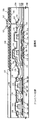
本願発明の実施形態について、図1を用いて以下に説明する。図1は同一基板上にドライバー回路と画素部とを一体形成したAM−LCDの断面図を示している。なお、ここではドライバー回路を構成する基本回路としてCMOS回路を示し、画素TFTとしてはダブルゲート構造のTFTを示している。勿論、トリプルゲート構造やシングルゲート構造としてもよい。
【0024】
図1において、100は耐熱性を有する基板であり、ガラス基板、石英基板、プラスチック基板、シリコン基板、セラミックス基板、金属基板(代表的にはステンレス基板)を用いれば良い。どの基板を用いる場合においても、必要に応じて下地膜(好ましくは珪素を主成分とする絶縁膜)を設けても構わない。なお、マスク数を低減するために裏面露光を用いる場合は、透光性を有する基板が望ましい。
【0025】
101は遮蔽層であり、その上に下地膜が形成される。遮蔽層は画素部に設けられ、TFTのチャネル形成領域を光または電磁波等から保護する。なお、遮蔽層の材料としては遮光性(吸光度=3以上)を有していればどのような材料を用いても構わない。ただし、後のプロセス温度に耐えうる耐熱性を有する材料であることが望ましい。
【0026】
102は下地膜として設けた酸化珪素膜であり、その上にドライバーTFTの活性層、画素TFTの活性層となる半導体層が形成される。そして、活性層を覆ってゲート絶縁膜103が形成され、その上にゲート電極が形成される。なお、本明細書中において「電極」とは、「配線」の一部であり、他の配線との電気的接続を行う箇所、または半導体層と交差する箇所を指す。従って、説明の便宜上、「配線」と「電極」とを使い分けるが、「配線」という文言に「電極」は常に含められているものとする。
【0027】
図1において、ドライバーTFTの活性層は、Nチャネル型TFT(以下、NTFTという)のソース領域104、ドレイン領域105、LDD(ライトドープトドレイン)領域106およびチャネル形成領域107、並びにPチャネル型TFT(以下、PTFTという)のソース領域108、ドレイン領域109およびチャネル形成領域110で形成される。また、ドライバーTFTのLDD領域106の幅(チャネル長方向)は0.05〜0.5μm(好ましくは0.1〜0.3μm)に形成されている。加えて、本発明においてはドライバーTFTのNチャネル型TFTのLDD領域106をゲート電極115と一部重ならせた構造(GOLD構造)として、ホットキャリア耐性を向上させている。
【0028】
また、画素TFT(ここではNTFTを用いる。)の活性層は、ソース領域またはドレイン領域111、112、LDD領域113およびチャネル形成領域114で形成される。また、画素TFTのLDD領域113の幅は、ドライバーTFTのLDD領域106の幅と異なる。なお、画素TFTのLDD領域113はゲート電極115と重ならない構造(LDD構造)として、オフ電流を低減させて信頼性を向上させている。
【0029】
なお、本明細書中において、ゲート電圧が印加されるLDD領域を有する構造をGOLD構造と呼ぶ。一方、ゲート電圧が印加されないLDD領域のみを有する構造をLDD構造と呼ぶ。
【0030】
加えて、本発明においては、同一基板上に形成されたAM−LCDに代表される電気光学装置における各回路の機能に応じた濃度で不純物を添加して各回路のTFTの低濃度不純物領域を形成することを特徴とする。
【0031】
ドライバーTFTのNチャネル型TFTのLDD領域106には、半導体層に対して15族に属する元素が添加され、本願発明では、このLDD領域に添加される15族に属する元素の濃度、例えばリンが1×10¹⁶〜5×10¹⁸atoms/cm3の濃度で存在することを特徴としている。ドライバーTFTのLDD領域のリン濃度は画素TFTのLDD領域におけるリン濃度の2〜10倍とすることが望ましい。このような濃度とすることで、ドライバーTFTの移動度のさらなる向上が実現可能となる。
【0032】
一方、画素TFTのLDD領域113には、ドライバーTFTのNチャネル型TFTのLDD領域106と比較して15族に属する元素を低濃度に添加することを特徴としている。このようにすることで、画素TFTのさらなるオフ電流の低下が実現可能となる。
【0033】
また、ここでは、各TFTのゲート絶縁膜116を同じ膜厚の同一絶縁膜としたが、特に限定されない。例えば、回路特性に応じて同一基板上に異なるゲート絶縁膜を有するTFTが少なくとも二種類以上存在する構成としてもよい。
【0034】
ゲート電極115の材料としては、導電性を有していればどのような材料でも使用可能であるが、代表的には、導電性を有する珪素膜(例えばリンドープシリコン膜、ボロンドープシリコン膜等)や金属膜(例えばタングステン膜、タンタル膜、モリブデン膜、チタン膜等)でも良いし、前記金属膜をシリサイド化したシリサイド膜、窒化した金属膜(窒化タンタル膜、窒化タングステン膜、窒化チタン膜等)でも良い。また、これらを自由に組み合わせて積層しても良い。
【0035】
また、上記金属膜をゲート電極115の材料として用いる場合には、金属膜の酸化を防止するために珪素膜との積層構造とすることが望ましい。また、酸化防止という意味では、金属膜を窒化珪素膜で覆った構造が有効である。
【0036】
次に、117は第1層間絶縁膜であり、珪素を含む絶縁膜(単層または積層)で形成される。珪素を含む絶縁膜としては、酸化珪素膜、窒化珪素膜、酸化窒化珪素膜(酸素よりも窒素の含有量の方が多い)、窒化酸化珪素膜(窒素よりも酸素の含有量の方が多い)を用いることができる。
【0037】
そして、第1層間絶縁膜117にはコンタクトホールが設けられ、ドライバーTFTのソース配線118、120、ドレイン配線119、および画素TFTのソース配線またはドレイン配線121、122が形成される。その上にはパッシベーション膜123、第2層間絶縁膜124が形成される。その上には保持容量を形成するために設けられた透明導電膜125と、誘電体となる絶縁膜126が積層形成される。なお、透明導電膜125は固定電位にしておくか、フローティング状態(電気的に独立した状態)にしておく。さらに、平坦化のための第3層間絶縁膜127を形成し、コンタクトホールを設けた後、画素電極128が形成される。
【0038】
また、ここでは保持容量を透明導電膜125、絶縁膜126、画素電極128とで形成したが、特に限定されない。例えば、容量配線を設ける構成、高濃度不純物領域112を延在させて上部電極とする構成、第2層間絶縁膜124上に導電材料からなる遮蔽膜を形成し上部電極とする構成を用いることができる。
【0039】
また、必要に応じて、各TFTの上にゲート配線と同様の材料を用いた遮蔽膜を設ける構成としても良いし、対向基板に遮蔽膜を設けるような構造としても良い。
【0040】
第2層間絶縁膜124や第3層間絶縁膜127としては、比誘電率の小さい樹脂膜が好ましい。樹脂膜としては、ポリイミド膜、アクリル膜、ポリアミド膜、BCB(ベンゾシクロブテン)膜などを用いることができる。
【0041】
また、絶縁膜としては、珪素を主成分とする絶縁膜、または遮蔽膜の酸化膜が好ましい。絶縁膜126の形成方法としてはスパッタ法、高圧酸化法、陽極酸化法等の公知な技術を用いて形成すればよい。
【0042】
また、画素電極128としては、透過型AM−LCDを作製するのであればITO膜に代表される透明導電膜を、反射型AM−LCDを作製するのであればアルミニウム膜に代表される反射率の高い金属膜を用いれば良い。
【0043】
なお、図1では画素電極128がドレイン電極122を介して画素TFTのドレイン領域112と電気的に接続されているが、画素電極128とドレイン領域112とが直接的に接続するような構造としても良い。
【0044】
また、ここでは、画素部のみに遮蔽層を形成した例を示したが、ドライバー回路のうち、サンプリング回路などは、オフ電流の小さいTFTを用いる方が望ましいので、遮蔽層を形成してTFTを形成することが望ましい。
【0045】
以上のような構造でなるAM−LCDは、移動度の高いGOLD構造のNTFTを備えたドライバー回路と、オフ電流の低いLDD構造のNTFTを備えた画素部とを備えた点に特徴がある。こうすることで、同一基板上に移動度を優先するTFTと、オフ電流の小さいTFTとを機能に応じた回路に適用して、高い駆動能力と高い信頼性を有する電気光学装置を実現することが可能である。
【0046】
以上の構成でなる本願発明について、以下に示す実施例でもってさらに詳細な説明を行うこととする。
【0047】
【実施例】
[実施例1]
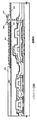
本実施例では、「発明の実施の形態」で説明した図1の構造を実現するための作製工程について説明する。説明には図2〜5を用いる。
【0048】
まず、基板として透光性を有する石英基板200を用意し、その上に遮光性を有する材料層を形成した後、パターニングによって遮蔽層201とアライメントマーク(図示しない)とを同時形成した。この遮蔽層は、画素部に形成し、後の裏面露光工程で画素部におけるLDD領域の幅を決定するため重要である。
【0049】
遮蔽層201としては、金属膜(例えばタングステン膜、タンタル膜、モリブデン膜、チタン膜等)や、前記金属膜をシリサイド化したシリサイド膜、窒化した金属膜(窒化タンタル膜、窒化タングステン膜、窒化チタン膜等)等を用いる。
また、これらを自由に組み合わせて積層しても良い。なお、段差によるカバレッジ不良を防ぐために遮蔽層はテーパー形状とすることが好ましい。
【0050】
次いで、200nm厚の酸化珪素膜(下地膜とも呼ぶ)201と50nm厚の非晶質珪素膜203aとを大気解放しないまま連続的に成膜した。(図2(A))こうすることで非晶質珪素膜203aの下表面に大気中に含まれるボロン等の不純物が吸着することを防ぐことができる。
【0051】
なお、本実施例では非晶質珪素(アモルファスシリコン)膜を用いたが、他の半導体膜であっても構わない。微結晶珪素(マイクロクリスタルシリコン)膜でも良いし、非晶質シリコンゲルマニウム膜でも良い。また、下地膜及び半導体膜の形成手段としては、PCVD法、LPCVD法またはスパッタ法等を用いることができる。
【0052】
次に、非晶質珪素膜の結晶化を行う。本発明においては、如何なる公知の結晶化技術、例えば熱結晶化、赤外光または紫外光の照射による結晶化、触媒元素を用いた熱結晶化、触媒元素を用いたレーザー結晶化等を用いてよい。本実施例では結晶化手段として、特開平9−312260号公報に記載された技術を用いた。
同公報に記載された技術は、珪素膜の結晶化を助長する触媒元素としてニッケル、コバルト、パラジウム、ゲルマニウム、白金、鉄、銅から選ばれた元素を用いている。
【0053】
まず、非晶質珪素膜上に酸化珪素膜を形成し、パターニングして開口部を有するマスク204を形成する。非晶質珪素膜203aとマスクとなる酸化珪素膜とを大気解放しないまま連続的に成膜することが好ましい。そして、露呈した非晶質珪素膜上にニッケルを含んだ層を形成し、脱水素化処理を行った後、500〜650℃、4〜16時間の熱処理を行い結晶化させる。この結晶化の過程ではニッケルが接した非晶質珪素膜の部分が最初に結晶化し、そこから横方向(図2(B)中に示した矢印の方向)へと結晶化が進行する。本実施例では、重量換算で10ppmのニッケルを含む酢酸ニッケル塩溶液を塗布した後、450℃、1時間の脱水素化処理を行った後に600℃、12時間の熱処理を行って結晶化し結晶質珪素膜203bを形成した。(図2(B))
【0054】
なお、酸化珪素膜からなるマスク204を設けておくことで、活性層が有機物で汚染されることを防げる。次いで、そのままマスク204を用いて、15族に属する元素(本実施例ではリン)の添加工程を行う。添加するリンの濃度は5×10¹⁸〜1×10²⁰atoms/cm3(好ましくは1×1019〜5×1019atoms/cm3)が好ましい。但し、添加すべきリンの濃度は、後のゲッタリング工程の温度、時間、さらにはリンドープ領域の面積によって変化するため、この濃度範囲に限定されるものではない。こうしてリンが添加された領域(以下、リンドープ領域という)203cが形成された。(図2(C))
【0055】
次いで、500〜650℃の熱処理を2〜16時間加え、珪素膜の結晶化に用いた触媒元素(本実施例ではニッケル)のゲッタリングを行う。ゲッタリング作用を奏するためには熱履歴の最高温度から±50℃程度の温度が必要であるが、結晶化のための熱処理が550〜600℃で行われるため、500〜650℃の熱処理で十分にゲッタリング作用を奏することができる。本実施例では600℃、8時間の熱処理を加えることによってニッケルが矢印(図2(D)に示す)の方向に移動し、リンドープ領域203cに含まれるリンによってゲッタリングされて捕獲された。こうしてゲッタリング領域(リンドープ領域203bに対応する領域)が形成される。これにより203dで示した領域に含まれるニッケルの濃度は2×10¹⁷atoms/cm3以下(好ましくは1×1016atoms/cm3以下)にまで低減される。また、このゲッタリング領域は、後のパターニングの際に除去される。
【0056】
次いで、マスク204を除去した後、形成された結晶質珪素(ポリシリコン)膜をパターニングして、ドライバーTFTの半導体層205a、205b、画素TFTの半導体層206を形成した。(図3(A))
【0057】
なお、ドライバーTFTおよび画素TFTの半導体層を形成する前後に、結晶質珪素膜に対してTFTのしきい値電圧を制御するための不純物元素(リンまたはボロン)を添加しても良い。この工程はNTFTまたはPTFTのみに行っても良いし、双方に行っても良い。
【0058】
次に、プラズマCVD法またはスパッタ法によりゲート絶縁膜207を形成する。このゲート絶縁膜207はTFTのゲート絶縁膜として機能することになる絶縁膜であり、膜厚は50〜200nmとする。本実施例では70nm厚の酸化珪素膜を用いた。また、酸化珪素膜のみでなく酸化珪素膜の上に窒化珪素膜を設けた積層構造とすることもできるし、酸化珪素膜に窒素を添加した酸化窒化珪素膜を用いても構わない。
【0059】
ゲート絶縁膜207を形成したら、ドライバー回路のNTFTのチャネル形成領域210、及び画素部、ドライバー回路のPTFT上にレジストマスク208a〜cを設けた後、15族に属する元素(本実施例ではリン)を添加してドライバーTFTのNTFTの低濃度不純物領域209を形成する。(図3(B))この低濃度不純物領域209に添加されるリンの濃度は5×10¹⁷〜5×10¹⁸atoms/cm3となるように調節する。この時のリンの濃度がドライバー回路のNTFTのLDD領域における濃度を決定する。
【0060】
また、リンの添加工程は、質量分離を行うイオンインプランテーション法を用いても良いし、質量分離を行わないプラズマドーピング法を用いても良い。また、加速電圧やドーズ量の条件等は実施者が最適値を設定すれば良い。本実施例では水素で1〜10%に希釈したフォスフィンをドーピングガスとして用い、ドーズ量4×10¹³atoms/cm2、加速電圧は80kVとした。
【0061】
次に、レジストマスク208a〜cを除去した後、不純物の活性化を行った。活性化処理としては、不活性雰囲気または酸素雰囲気で300〜700℃の温度範囲で2時間程度の熱処理で十分であるが、700〜1150℃ここでは、800℃、2時間の加熱処理を行い、十分な活性化とともに結晶性の改善を行った。この工程において、大気中または酸素雰囲気中で行えば活性化と同時に熱酸化される。なお、本実施例では2回に分けて活性化を行うが、後に形成するゲート電極が活性化の熱温度に耐えられる材料であれば、1回の活性化で済むため工程数を低減できる。
【0062】
こうして活性化工程を終了したら、次に導電膜211を形成した。(図3(C))次いで、パターニングを行いドライバーTFTのゲート配線212a(NTFT側)、画素TFTのゲート配線212cを形成する。なお、ゲート配線212cは画素TFTがダブルゲート構造であるためゲート配線を2本記載しているが、実際には同一配線である。また、ドライバーTFTのPTFT全体を覆った導電層212aを形成する。
【0063】
また、本実施例では配線212a〜cとして、下層から窒化タンタル膜/タンタル膜/窒化タンタル膜(または下層から窒化タンタル膜/タンタル膜)という積層膜を用いた。勿論、「発明の実施の形態」で説明した他の導電膜を用いることも可能であることは言うまでもない。また、本実施例では、ゲート配線の膜厚は300nmとした。
【0064】
次いで、配線212a〜cをマスクとして、15族に属する元素を添加し、自己整合的に低濃度不純物領域214が形成された。(図3(D))この低濃度不純物領域214に添加される不純物の濃度、ここではリンの濃度が5×10¹⁷〜5×10¹⁸atoms/cm3となるように調節する。ただし、この工程は先のリンの添加工程よりも低いドーズ量5×1012〜1×1013atoms/cm2で添加する。この時、添加された15族に属する元素の濃度が画素部のLDD領域の濃度を決定する。
【0065】
また、図3(B)で示した工程と同様に、リンの添加工程は質量分離を行うイオンインプランテーション法を用いても良いし、質量分離を行わないプラズマドーピング法を用いても良い。また、加速電圧やドーズ量の条件等は実施者が最適値を設定すれば良い。
【0066】
次に、裏面露光によりレジストマスクを形成する。(図4(A))この時、画素部においては、遮蔽層201がマスクとなりレジストマスク217c、217dを形成する一方、ドライバーTFTのNTFTにおいては、ゲート電極がマスクとなりレジストマスク217bを形成する。また、PTFTにおいては、導電層がマスクとなりレジストマスク217aを形成する。
【0067】
また、本実施例では裏面露光を用いてレジストマスク217の形成を行ったが特に限定されず、フォトマスクを用いたレジストマスクを用いてもよい。
【0068】
こうして裏面露光により得られたレジストマスク217a〜cをマスクとして不純物のドーピングを高濃度に行う。(図4(B))不純物領域219〜223に添加されるリンの濃度は5×10¹⁹〜1×10²¹atoms/cm3となるように調節する。
【0069】
この工程によりCMOS回路を形成するNTFTのソース領域218、LDD領域225、チャネル形成領域226が画定する。また、画素TFTのソース領域227、ドレイン領域228、LDD領域229a、229b、チャネル形成領域230a、230bが画定する。
【0070】
このように、3回に分けて、15族に属する元素(本実施例ではリン)を添加して、各不純物領域を形成する。
【0071】
この後、レジストマスク224a、224bを形成してパターニングを行いPTFTのゲート電極225を形成する。このレジストマスク224bは、CMOS回路のPTFTとなる領域以外を覆っている。そして、このレジストマスクをそのまま用いて13族に属する元素(本実施例ではボロン)の添加を行い、ソース領域227、ドレイン領域228を形成する。(図4(C))具体的には、1×10²⁰〜3×10²¹atoms/cm3の濃度でボロンが添加されるように調節する。本実施例では水素で1〜10%に希釈されたジボランを用いた。
【0072】
この工程によりCMOS回路を形成するPTFTのソース領域227、ドレイン領域228、チャネル形成領域226が画定する。
【0073】
勿論、ボロンの添加工程も質量分離を行うイオンインプランテーション法を用いても良いし、質量分離を行わないプラズマドーピング法を用いても良い。また、加速電圧やドーズ量の条件等は実施者が最適値を設定すれば良い。
【0074】
こうして全ての不純物領域を形成し終えたら、レジストマスク224a、224bを除去する。そして、添加した不純物の活性化をレーザーアニール、熱アニール、ファーネスアニール、ランプアニール処理等により行う。ここでは、大気雰囲気中においてエキシマレーザー光を用いてエネルギー密度187mJ/cm2のレーザーアニール処理を行った。また、熱アニールによる活性化を行った場合、添加されたリンのゲッタリング作用によって活性化と同時にチャネル形成領域における触媒元素の低減も図ることができる。ただし、ゲッタリング作用を奏するためには熱履歴の最高温度から±50℃程度の温度が必要である。
【0075】
次いで、第1層間絶縁膜249を形成する。本実施例では、プラズマCVD法により形成した1μm厚の酸化珪素膜を用いた。そして、コンタクトホールを形成した後、ソース配線230、232、233、ドレイン配線231、234を形成した。これらの配線はアルミニウムを主成分とする導電膜をチタン膜で挟んだ積層膜で形成した。(図5(A))
【0076】
この時、ドレイン配線231はCMOS回路を形成するNTFTおよびPTFTに共通の配線として用いられる。
【0077】
その後、パッシベーション膜235を形成する。パッシベーション膜235としては、窒化珪素膜、酸化窒化珪素膜、窒化酸化珪素膜、またはこれらの絶縁膜と酸化珪素膜との積層膜を用いることができる。本実施例では300nm厚の窒化珪素膜をパッシベーション膜として用いた。
【0078】
なお、本実施例では窒化珪素膜を形成する前処理として、水素を含むガス(本実施例ではアンモニアガス)を用いたプラズマ処理を行うことは有効である。この前処理によりプラズマによって活性化した(励起した)水素が活性層(半導体層)内に閉じこめられるため、効果的に水素終端が行われる。
【0079】
さらに、水素を含むガスに加えて亜酸化窒素ガスを加えると、発生した水分によって被処理体の表面が洗浄され、特に大気中に含まれるボロン等による汚染を効果的に防ぐことができる。
【0080】
パッシベーション膜235を形成したら、開口率を向上させるために、本実施例では、画素表示領域のパッシベーション膜を選択的に除去した。その上に第2層間絶縁膜236として1μm厚のアクリル膜を形成した。そして、その上に導電膜237、本実施例ではITO膜を形成してパターニングを行い、保持容量の下部電極を形成し、その上に誘電体となる酸化珪素からなる絶縁膜238をスパッタ法により積層形成した。なお、導電膜237は固定電位にしておくか、フローティング状態(電気的に独立した状態)にしておく。
【0081】
次に、第3層間絶縁膜239として再び1μm厚のアクリル膜を形成してパターニングを行い、保持容量を形成する領域のアクリル膜を選択的に除去し、且つ、同時にコンタクトホールを形成し、ITO膜でなる画素電極240を形成した。
保持容量は、導電膜237と、絶縁膜238と、画素電極240とで形成される。なお、絶縁膜238は薄いため、薄い有機樹脂膜を積層形成して保護してもよい。こうして図5(C)に示すような構造のAM−LCDが完成する。
【0082】
このように本願発明は、ドーズ量の異なる不純物の添加を3回以上行って、各回路の機能に適したNTFTの構造及びLDD領域の不純物濃度を形成し、移動度の高いGOLD構造のNTFTを少なくとも一つ以上備えたドライバー回路と、オフ電流の低いLDD構造のNTFTを備えた画素部とを形成する点に特徴がある。
【0083】
図6は、AM−LCDの回路構成の一例を示す。本実施例のAM−LCDは、ソース信号線側ドライバー回路601、ゲート信号線側ドライバー回路(A)607、ゲート信号線側ドライバー回路(B)611、プリチャージ回路612、画素部606を有している。
【0084】
ソース信号線側ドライバー回路601は、シフトレジスタ回路602、レベルシフタ回路603、バッファ回路604、サンプリング回路605を備えている。
【0085】
また、ゲート信号線側ドライバー回路(A)607は、シフトレジスタ回路608、レベルシフタ回路609、バッファ回路610を備えている。ゲート信号線側ドライバー回路(B)611も同様な構成である。
【0086】
具体的には、高移動度を優先する回路であるシフトレジスタ回路602、608のNTFTは本発明のGOLD構造とし、レベルシフタ回路603、609バッファ回路604、610、サンプリング回路605、画素部606のNTFTは、本発明のLDD構造とした。このように、ドライバー回路においても、各回路に応じてGOLD構造またはLDD構造とすることが望ましい。また、ドライバー回路の下方または上方に遮蔽層を形成する構成としてもよく、特にサンプリング回路においては安定なTFT特性が得られるので効果的である。
【0087】
本実施例の構成とすることによって、同一基板上に移動度を優先するTFTと、オフ電流の小さいTFTとを機能に応じた回路に適用して、高い駆動能力と高い信頼性を有する電気光学装置を実現することができた。
【0088】
また、ここではトップゲート型TFTを用いた例を示したが、本発明はTFT構造に関係なく適用することができ、例えば逆スタガ型TFTに適用することも可能である。
【0089】
また、本実施例の作製工程に従うと、最終的なTFTの活性層(半導体層)は、結晶格子に連続性を持つ特異な結晶構造の結晶質珪素膜で形成される。その特徴について以下に説明する。
【0090】
上記作製工程に従って形成した活性層は、微視的に見れば複数の針状又は棒状の結晶(以下、棒状結晶と略記する)が集まって並んだ結晶構造を有する。このことはTEM(透過型電子顕微鏡法)による観察で容易に確認できた。
【0091】
また、電子線回折及びエックス線(X線)回折を利用すると活性層の表面(チャネルを形成する部分)が、結晶軸に多少のずれが含まれているものの主たる配向面として{110}面を有することを確認できた。本出願人がスポット径約1.5μmの電子線回折写真を詳細に観察した結果、{110}面に対応する回折斑点がきれいに現れているが、各斑点は同心円上に分布を持っていることが確認された。
【0092】
また、本出願人は個々の棒状結晶が接して形成する結晶粒界をHR−TEM(高分解能透過型電子顕微鏡法)により観察し、結晶粒界において結晶格子に連続性があることを確認した。これは観察される格子縞が結晶粒界において連続的に繋がっていることから容易に確認できた。
【0093】
なお、結晶粒界における結晶格子の連続性は、その結晶粒界が「平面状粒界」と呼ばれる粒界であることに起因する。本明細書における平面状粒界の定義は、「Characterization of High-Efficiency Cast-Si Solar Cell Wafers by MBIC Measurement ;Ryuichi Shimokawa and Yutaka Hayashi,Japanese Journal of Applied Physics vol.27,No.5,pp.751-758,1988」に記載された「Planar boundary 」である。
【0094】
上記論文によれば、平面状粒界には双晶粒界、特殊な積層欠陥、特殊なtwist 粒界などが含まれる。この平面状粒界は電気的に不活性であるという特徴を持つ。即ち、結晶粒界でありながらキャリアの移動を阻害するトラップとして機能しないため、実質的に存在しないと見なすことができる。
【0095】
特に結晶軸(結晶面に垂直な軸)が〈110〉軸である場合、{211}双晶粒界はΣ3の対応粒界とも呼ばれる。Σ値は対応粒界の整合性の程度を示す指針となるパラメータであり、Σ値が小さいほど整合性の良い粒界であることが知られている。
【0096】
本出願人が本実施例を実施して得た結晶質珪素膜を詳細にTEMを用いて観察した結果、結晶粒界の殆ど(90%以上、典型的には95%以上)がΣ3の対応粒界、即ち{211}双晶粒界であることが判明した。
【0097】
二つの結晶粒の間に形成された結晶粒界において、両方の結晶の面方位が{110}である場合、{111}面に対応する格子縞がなす角をθとすると、θ=70.5°の時にΣ3の対応粒界となることが知られている。
【0098】
本実施例の結晶質珪素膜は、結晶粒界において隣接する結晶粒の各格子縞がまさに約70.5°の角度で連続しており、その事からこの結晶粒界は{211}双晶粒界であるという結論に辿り着いた。
【0099】
なお、θ= 38.9 °の時にはΣ9の対応粒界となるが、この様な他の結晶粒界も存在した。
【0100】
この様な対応粒界は、同一面方位の結晶粒間にしか形成されない。即ち、本実施例を実施して得た結晶質珪素膜は面方位が概略{110}で揃っているからこそ、広範囲に渡ってこの様な対応粒界を形成しうる。
【0101】
この様な結晶構造(正確には結晶粒界の構造)は、結晶粒界において異なる二つの結晶粒が極めて整合性よく接合していることを示している。即ち、結晶粒界において結晶格子が連続的に連なり、結晶欠陥等に起因するトラップ準位を非常に作りにくい構成となっている。従って、この様な結晶構造を有する半導体薄膜は実質的に結晶粒界が存在しないと見なすことができる。
【0102】
また、さらに、700〜1150℃という高い温度での熱処理工程(本実施例における熱酸化工程またはゲッタリング工程にあたる)によって結晶粒内に存在する欠陥が殆ど消滅していることがTEM観察によって確認されている。これはこの熱処理工程の前後で欠陥数が大幅に低減されていることからも明らかである。
【0103】
この欠陥数の差は電子スピン共鳴分析(Electron Spin Resonance :ESR)によってスピン密度の差となって現れる。現状では本実施例の作製工程に従って作製された結晶質珪素膜のスピン密度は少なくとも 5×10¹⁷spins/cm3以下(好ましくは 3×10¹⁷spins/cm3以下)であることが判明している。ただし、この測定値は現存する測定装置の検出限界に近いので、実際のスピン密度はさらに低いと予想される。
【0104】
以上の事から、本実施例を実施することで得られた結晶質珪素膜は結晶粒内及び結晶粒界が実質的に存在しないため、単結晶シリコン膜又は実質的な単結晶シリコン膜と考えて良い。
【0105】
(TFTの電気特性に関する知見)
本実施例で作製したTFTは、MOSFETに匹敵する電気特性を示した。本出願人が試作したTFT(但し、活性層の膜厚は30nm、ゲート絶縁膜の膜厚は100nm)からは次に示す様なデータが得られている。
【0106】
(1)スイッチング性能(オン/オフ動作切り換えの俊敏性)の指標となるサブスレッショルド係数が、Nチャネル型TFTおよびPチャネル型TFTともに60〜100mV/decade(代表的には60〜85mV/decade )と小さい。
(2)TFTの動作速度の指標となる電界効果移動度(μFE)が、Nチャネル型TFTで 200〜650cm2/Vs (代表的には 300〜500cm2/Vs )、Pチャネル型TFTで100〜300cm2/Vs(代表的には 150〜200cm2/Vs)と大きい。
(3)TFTの駆動電圧の指標となるしきい値電圧(Vth)が、Nチャネル型TFTで-0.5〜1.5 V、Pチャネル型TFTで-1.5〜0.5 Vと小さい。
【0107】
以上の様に、極めて優れたスイッチング特性および高速動作特性が実現可能であることが確認されている。
【0108】
(回路特性に関する知見)
次に、本実施例を実施して形成したTFTを用いて作製されたリングオシレータによる周波数特性を示す。リングオシレータとはCMOS構造でなるインバータ回路を奇数段リング状に接続した回路であり、インバータ回路1段あたりの遅延時間を求めるのに利用される。実験に使用したリングオシレータの構成は次の様になっている。
段数:9段
TFTのゲート絶縁膜の膜厚:30nm及び50nm
TFTのゲート長(チャネル長): 0.6μm
【0109】
このリングオシレータによって発振周波数を調べた結果、最大値で約1GHzの発振周波数を得ることができた。また、実際にLSI回路のTEGの一つであるシフトレジスタを作製して動作周波数を確認した。その結果、ゲート絶縁膜の膜厚30nm、ゲート長 0.6μm、電源電圧5V、段数50段のシフトレジスタ回路において動作周波数100MHzの出力パルスが得られた。
【0110】
以上の様なリングシレータおよびシフトレジスタの驚異的なデータは、本実施例のTFTがMOSFETに匹敵する、若しくは凌駕する性能(電気特性)を有することを示している。
【0111】
〔実施例2〕
本実施例では、実施例1において結晶質珪素膜の形成に他の手段を用いた場合について図7に説明する。
【0112】
具体的には、赤外光または紫外光の照射による結晶化処理(以下、レーザー結晶化と呼ぶ)を用いる。レーザー結晶化は基板にかけるストレスが少なく、短時間で処理することができるため有効である。レーザーのガスとしてXeCl、ArF、KrF等を用いたパルスレーザーやArレーザー等の連続発振レーザーや連続発光エキシマレーザー等を用いて照射する。なお、レーザー結晶化の条件(レーザービームの形状、レーザー光の波長、オーバーラップ率、照射強度、パルス幅、繰り返し周波数、照射時間等)は半導体膜の膜厚、基板温度等を考慮して実施者が適宜決定すればよい。
【0113】
まず、基板701に酸化シリコン膜702を設け、その上に非晶質珪素膜703を形成した。(図7(A))次に、500℃、1時間の脱水素工程の後、レーザー結晶化処理を行い、結晶質珪素膜705を形成した。(図7(B))
【0114】
本実施例と実施例1と異なっている点は、触媒元素を用いることなくレーザー結晶化を行っている点である。
【0115】
以降の工程は実施例1に従えば、本願発明のTFTの構成を得ることができる。ただし、実施例1では触媒元素の低減処理(ゲッタリング)を行っているが、本実施例においては特に必要ない。
【0116】
〔実施例3〕
本実施例では、実施例1において結晶質珪素膜の形成に他の手段を用いた場合について図8に説明する。なお、簡略化のため、ドライバー回路の領域のみ示し、画素部の遮蔽層は図示しない。
【0117】
具体的には、非晶質珪素膜の結晶化に特開平7−130652号公報(米国特許番号08/329,644に対応)に記載された技術を用いる。同公報に記載された技術は、結晶化を促進する触媒元素(代表的にはニッケル)を非晶質珪素膜の表面に保持させて結晶化を行う技術である。
【0118】
まず、基板801に酸化シリコン膜802を設け、その上に非晶質珪素膜803を形成した。さらに重量換算で10ppmのニッケルを含む酢酸ニッケル塩溶液を塗布して、ニッケル含有層804を形成した。(図8(A))
【0119】
次に、500℃、1時間の脱水素工程の後、500〜650℃で4〜12時間の熱処理を行い、結晶質珪素膜805を形成した。(図8(B))こうして得られた結晶質珪素膜805は非常に優れた結晶性を有した。本願発明のTFTの構成を得るためには、以降の工程は実施例1に従えば良い。
【0120】
なお、本実施例の構成は実施例1〜2のいずれの構成とも自由に組み合わせることが可能である。
【0121】
〔実施例4〕
本実施例では、実施例1において結晶質珪素膜及びゲート絶縁膜の形成に他の手段を用いた場合について図9に説明する。なお、簡略化のため、ドライバー回路の領域のみ示し、画素部の遮蔽層は図示しない。
【0122】
ここでは、少なくとも700〜1100℃程度の耐熱性を有する基板が必要であり、石英基板901を用いた。そして、実施例1及び3で示した技術を用い、結晶質半導体膜が形成され、これをTFTの活性層にするために島状にパターニングして半導体層902、903を形成した。そして、半導体層902、903を覆ってゲート絶縁膜904を、酸化珪素膜を主成分とする膜で形成した。本実施例では、プラズマCVD法で窒化酸化珪素膜を70nmの厚さで形成した。(図9(A))
【0123】
そして、ハロゲン(代表的には塩素)と酸素を含む雰囲気中で熱処理を行った。本実施例では950℃、30分とした。尚、処理温度は700〜1100℃の範囲で選択すればよく、処理時間も10分〜8時間の間で選択すれば良かった。
【0124】
その結果、本実施例の条件では半導体層905、906とゲート絶縁膜904との界面で熱酸化膜が形成され、ゲート絶縁膜907が形成された。(図9(B))また、ハロゲン雰囲気での酸化の過程で、ゲート絶縁膜904と半導体層902、903に含まれる不純物で、特に金属不純物元素はハロゲンと化合物を形成し、気相中に除去することができた。
【0125】
以上の工程で作製されたゲート絶縁膜907は、絶縁耐圧が高く半導体層905、906とゲート絶縁膜907の界面は非常に良好なものであった。本願発明のTFTの構成を得るためには、以降の工程は実施例1に従えば良い。
【0126】
なお、本実施例の構成は実施例1〜3のいずれの構成とも自由に組み合わせることが可能である。
【0127】
〔実施例5〕
本実施例では、実施例1において結晶質珪素膜中の触媒元素の低減に他の手段を用いた場合について説明する。
【0128】
実施例1においては、リン元素を選択的に添加した後に加熱処理を行い結晶質珪素膜中の触媒元素の低減するゲッタリングを行ったが、リン元素を全面に添加してもよいことは勿論である。本実施例では、高温の硫酸を用いた液相を接触させることによりゲッタリングする方法を示す。
【0129】
まず、実施例1の工程に従って図3(A)の状態を得た。次いで、基板ごと300℃に加熱した液相中(本実施例では硫酸溶液中)に浸し、結晶化に用いたニッケルを除去または低減する。なお、硫酸と半導体層を接触させる方法は特に限定されない。
【0130】
このようにして、液相による触媒元素の低減処理を行うことで、触媒元素の濃度を短時間で低減することができる。本願発明のTFTの構成を得るためには、以降の工程は実施例1に従えば良い。
【0131】
なお、本実施例の構成は実施例1〜4のいずれの構成とも自由に組み合わせることが可能である。
【0132】
〔実施例6〕
本実施例では、実施例1での透明電極125に代えて、導電性を有する遮蔽層(ブラックマスクとも呼ぶ)301を用いた例について図10に示す。この遮蔽層は外部からの光を遮るとともに、電界遮蔽の効果も有している。
【0133】
まず、実施例1に従い、第2の層間絶縁膜を形成する。次いで、チタンを主成分とする金属膜をスパッタ法により成膜した後、パターニングを行い画素TFTを覆うブラックマスク301を形成する。第2の層間絶縁膜に有機樹脂をもちいた場合、金属膜との密着性を向上させるためCF4ガスを用いたプラズマ処理を施してもよいし、第2の層間絶縁膜上にバッファ層となる薄い絶縁膜をスパッタ法等により形成してもよい。
【0134】
次いで、ブラックマスク301上に実施例1と同様にスパッタ法により酸化珪素膜302を形成する。ブラックマスク301は保持容量の下部電極となり、酸化珪素膜302は保持容量の誘電体となる。なお、ブラックマスク301は固定電位にしておくか、フローティング状態(電気的に独立した状態)にしておく。
【0135】
そして、後で画素電極とドレイン電極のコンタクト形成を容易とするために、選択的に酸化珪素膜302を除去した後、有機樹脂膜を形成する。その後、コンタクトホールを形成すると同時に、ブラックマスク上方の有機樹脂膜を選択的に除去して、第3層間絶縁膜304を形成する。この第3層間絶縁膜304は、ブラックマスク301と画素電極303との間に生じるショート(短絡)を効果的に防ぐ役目を果たしている。
【0136】
最後に透明導電膜からなる画素電極303を形成する。この画素電極303が、保持容量の上部電極となる。
【0137】
このような構成とすることで、十分な保持容量の形成が可能となり、TFTの光劣化をも防止できる。
【0138】
また、本実施例では、スパッタ法による酸化珪素膜を用いたが、ブラックマスクを高圧酸化または陽極酸化等の酸化方法により酸化して、その酸化膜を誘電体とするとスループットが向上する。
【0139】
なお、本実施例の構成は実施例1〜5のいずれの構成とも自由に組み合わせることが可能である。
【0140】
〔実施例7〕
本実施例では、具体的な画素部の構成(トリプルゲート構造)の一例を図11に示す。遮蔽層401は半導体層402の下層に設けられ、半導体層402上にゲート配線403が設けられている。本発明においては、遮蔽層401の線幅は、ゲート配線403の線幅より広くする。404はドレイン電極、405はソース配線、406は絶縁層、407は画素電極である。なお、画素電極409は模様で示したが、簡略化のため、画素電極407、408、410は太線で囲まれた領域で示した。
【0141】
また、図11に対応する断面図を図12に示した。また、図12の符号は図11と同一のものを用いた。なお、透明導電膜501は固定電位にしておくか、フローティング状態(電気的に独立した状態)にしておく。保持容量は、透明導電膜501と、絶縁膜502と、画素電極407で構成されている。
【0142】
本実施例は、実施例1がダブルゲート構造であったのに対して、トリプルゲート構造としたのみであり、基本的な構造は同一である。従って、図11及び図12の構造を得るには、実施例1で示した作製方法を用いればよい。
【0143】
なお、本実施例の構成は実施例1〜6のいずれの構成とも自由に組み合わせることが可能である。
【0144】
〔実施例8〕
本実施例では、実施例1に示した作製工程で基板上にTFTを形成し、実際にAM−LCDを作製した場合について説明する。
【0145】
実施例1に従い図5(C)の状態が得られたら、画素電極240上に配向膜を80nmの厚さに形成する。次に、対向基板としてガラス基板上にカラーフィルタ、透明電極(対向電極)、配向膜を形成したものを準備し、それぞれの配向膜に対してラビング処理を行い、シール材(封止材)を用いてTFTが形成された基板と対向基板とを貼り合わせる。そして、その間に液晶を保持させる。このセル組み工程は公知の手段を用いれば良いので詳細な説明は省略する。
【0146】
なお、セルギャップを維持するためのスペーサは必要に応じて設ければ良い。
従って、対角1インチ以下のAM−LCDのようにスペーサがなくてもセルギャップを維持できる場合は特に設けなくても良い。
【0147】
次に、以上のようにして作製したAM−LCDの外観を図13に示す。図13に示すようにアクティブマトリクス基板と対向基板とが対向し、これらの基板間に液晶が挟まれている。アクティブマトリクス基板は基板1000上に形成された画素部1001、走査線側ドライバー回路1002、信号線側ドライバー回路1003を有する。
【0148】
走査線側ドライバー回路1002、信号線側ドライバー回路1003はそれぞれ走査線1030、信号線1040によって画素部1001に接続されている。これらドライバー回路1002、1003はCMOS回路で主に構成されている。
【0149】
画素部1001の行ごとに走査線が形成され、列ごとに信号線1040が形成されている。走査線1030、信号線1040の交差部近傍には、画素TFT1010が形成されている。画素TFT1010のゲート電極は走査線1030に接続され、ソースは信号線1040に接続されている。さらに、ドレインには画素電極1060、保持容量1070が接続されている。
【0150】
対向基板1080は基板全面にITO膜等の透明導電膜が形成されている。透明導電膜は画素部1001の画素電極1060に対する対向電極であり、画素電極、対向電極間に形成された電界によって液晶材料が駆動される。対向基板1080には必要に応じて配向膜や、ブラックマスクや、カラーフィルターが形成されている。
【0151】
アクティブマトリクス基板側の基板にはFPC1031が外部出力端子1005に取り付けられ、ドライバー回路と外部出力端子を接続する配線1007、1008が形成されている。ビデオ信号の処理回路、タイミングパルス発生回路、γ補正回路、メモリ回路、演算回路などの回路をシリコン基板上に形成して構成されたICチップを設けてもよい。
【0152】
上記実施例によって作製された液晶表示装置には、TN液晶以外にも様々な液晶を用いることが可能である。例えば、1998, SID, "Characteristics and Driving Scheme of Polymer-Stabilized Monostable FLCD Exhibiting Fast Response Time and High Contrast Ratio with Gray-Scale Capability" by H. Furue et al.や、1997, SID DIGEST, 841, "A Full-Color Thresholdless Antiferroelectric LCD Exhibiting Wide Viewing Angle with Fast Response Time" by T. Yoshida et al.や、1996, J. Mater. Chem. 6(4), 671-673, "Thresholdless antiferroelectricity in liquid crystals and its application to displays" by S. Inui et al.や、米国特許第5594569 号に開示された液晶を用いることが可能である。
【0153】
さらに、本実施例では液晶表示装置を例に挙げて説明しているが、アクティブマトリクス型の表示装置であればEL(エレクトロルミネッセンス)表示装置やEC(エレクトロクロミックス)表示装置に本願発明を適用することも可能である。
【0154】
なお、本実施例は実施例1〜7のいずれの実施例とも自由に組み合わせることが可能である。
【0155】
〔実施例9〕
本実施例では、本願発明を用いてEL(エレクトロルミネッセンス)表示装置を作製した例について説明する。
【0156】
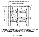
図14にアクティブマトリクス型ELディスプレイに適用した例を示す。
【0157】
図14はアクティブマトリクス型ELディスプレイの回路図である。11は表示領域を表しており、その周辺にはX方向周辺ドライバー回路12、Y方向周辺ドライバー回路13が設けられている。また、表示領域11の各画素は、スイッチ用TFT14、コンデンサ15、電流制御用TFT16、有機EL素子17を有し、スイッチ用TFT14にX方向信号線18a(または18b)、Y方向信号線20a(または20b、20c)が接続される。また、電流制御用TFT16には、電源線19a、19bが接続される。
【0158】
本実施例のアクティブマトリクス型ELディスプレイでは、X方向周辺ドライバー回路12、Y方向周辺ドライバー回路13に用いられるTFTの構造がGOLD構造であり、スイッチ用TFT14や電流制御用TFT16のTFT構造がLDD構造となっている。
【0159】
図15(A)は本願発明を用いたEL表示装置の上面図である。図15(A)において、4010は基板、4011は画素部、4012はソース線側ドライバー回路、4013はゲート線側ドライバー回路であり、それぞれのドライバー回路は配線4014〜4016を経てFPC4017に至り、外部機器へと接続される。
【0160】
このとき、少なくとも画素部、好ましくはドライバー回路及び画素部を囲むようにしてカバー材6000、シーリング材(ハウジング材ともいう)7000、密封材(第2のシーリング材)7001が設けられている。
【0161】
また、図15(B)は本実施例のEL表示装置の断面構造であり、基板4010、下地膜4021の上にドライバー回路用TFT(但し、ここではnチャネル型TFTとpチャネル型TFTを組み合わせたCMOS回路を図示している。)4022及び画素部用TFT4023(但し、ここではEL素子への電流を制御するTFTだけ図示している。)が形成されている。
【0162】
本願発明は、ドライバー回路用TFT4022、画素部用TFT4023に際して用いることができる。
【0163】
本願発明を用いてドライバー回路用TFT4022、画素部用TFT4023が完成したら、樹脂材料でなる層間絶縁膜(平坦化膜)4026の上に画素部用TFT4023のドレインと電気的に接続する透明導電膜でなる画素電極4027を形成する。透明導電膜としては、酸化インジウムと酸化スズとの化合物(ITOと呼ばれる)または酸化インジウムと酸化亜鉛との化合物を用いることができる。そして、画素電極4027を形成したら、絶縁膜4028を形成し、画素電極4027上に開口部を形成する。
【0164】
次に、EL層4029を形成する。EL層4029は公知のEL材料(正孔注入層、正孔輸送層、発光層、電子輸送層または電子注入層)を自由に組み合わせて積層構造または単層構造とすれば良い。どのような構造とするかは公知の技術を用いれば良い。また、EL材料には低分子系材料と高分子系(ポリマー系)材料がある。低分子系材料を用いる場合は蒸着法を用いるが、高分子系材料を用いる場合には、スピンコート法、印刷法またはインクジェット法等の簡易な方法を用いることが可能である。
【0165】
本実施例では、シャドーマスクを用いて蒸着法によりEL層を形成する。シャドーマスクを用いて画素毎に波長の異なる発光が可能な発光層(赤色発光層、緑色発光層及び青色発光層)を形成することで、カラー表示が可能となる。その他にも、色変換層(CCM)とカラーフィルターを組み合わせた方式、白色発光層とカラーフィルターを組み合わせた方式があるがいずれの方法を用いても良い。
勿論、単色発光のEL表示装置とすることもできる。
【0166】
EL層4029を形成したら、その上に陰極4030を形成する。陰極4030とEL層4029の界面に存在する水分や酸素は極力排除しておくことが望ましい。従って、真空中でEL層4029と陰極4030を連続成膜するか、EL層4029を不活性雰囲気で形成し、大気解放しないで陰極4030を形成するといった工夫が必要である。本実施例ではマルチチャンバー方式(クラスターツール方式)の成膜装置を用いることで上述のような成膜を可能とする。
【0167】
なお、本実施例では陰極4030として、LiF(フッ化リチウム)膜とAl(アルミニウム)膜の積層構造を用いる。具体的にはEL層4029上に蒸着法で1nm厚のLiF(フッ化リチウム)膜を形成し、その上に300nm厚のアルミニウム膜を形成する。勿論、公知の陰極材料であるMgAg電極を用いても良い。そして陰極4030は4031で示される領域において配線4016に接続される。配線4016は陰極4030に所定の電圧を与えるための電源供給線であり、導電性ペースト材料4032を介してFPC4017に接続される。
【0168】
4031に示された領域において陰極4030と配線4016とを電気的に接続するために、層間絶縁膜4026及び絶縁膜4028にコンタクトホールを形成する必要がある。これらは層間絶縁膜4026のエッチング時(画素電極用コンタクトホールの形成時)や絶縁膜4028のエッチング時(EL層形成前の開口部の形成時)に形成しておけば良い。また、絶縁膜4028をエッチングする際に、層間絶縁膜4026まで一括でエッチングしても良い。この場合、層間絶縁膜4026と絶縁膜4028が同じ樹脂材料であれば、コンタクトホールの形状を良好なものとすることができる。
【0169】
このようにして形成されたEL素子の表面を覆って、パッシベーション膜6003、充填材6004、カバー材6000が形成される。
【0170】
さらに、EL素子部を囲むようにして、カバー材6000と基板4010の内側にシーリング材が設けられ、さらにシーリング材7000の外側には密封材(第2のシーリング材)7001が形成される。
【0171】
このとき、この充填材6004は、カバー材6000を接着するための接着剤としても機能する。充填材6004としては、PVC(ポリビニルクロライド)、エポキシ樹脂、シリコーン樹脂、PVB(ポリビニルブチラル)またはEVA(エチレンビニルアセテート)を用いることができる。この充填材6004の内部に乾燥剤を設けておくと、吸湿効果を保持できるので好ましい。
【0172】
また、充填材6004の中にスペーサーを含有させてもよい。このとき、スペーサーをBaOなどからなる粒状物質とし、スペーサー自体に吸湿性をもたせてもよい。
【0173】
スペーサーを設けた場合、パッシベーション膜6003はスペーサー圧を緩和することができる。また、パッシベーション膜とは別に、スペーサー圧を緩和する樹脂膜などを設けてもよい。
【0174】
また、カバー材6000としては、ガラス板、アルミニウム板、ステンレス板、FRP(Fiberglass−Reinforced Plastics)板、PVF(ポリビニルフルオライド)フィルム、マイラーフィルム、ポリエステルフィルムまたはアクリルフィルムを用いることができる。なお、充填材6004としてPVBやEVAを用いる場合、数十μmのアルミニウムホイルをPVFフィルムやマイラーフィルムで挟んだ構造のシートを用いることが好ましい。
【0175】
但し、EL素子からの発光方向(光の放射方向)によっては、カバー材6000が透光性を有する必要がある。
【0176】
また、配線4016はシーリング材7000および密封材7001と基板4010との隙間を通ってFPC4017に電気的に接続される。なお、ここでは配線4016について説明したが、他の配線4014、4015も同様にしてシーリング材7000および密封材7001の下を通ってFPC4017に電気的に接続される。
【0177】
なお、本実施例は実施例1〜7のいずれの実施例とも自由に組み合わせることが可能である。
【0178】
〔実施例10〕
本願発明は従来のMOSFET上に層間絶縁膜を形成し、その上にTFTを形成する際に用いることも可能である。即ち、半導体回路上に反射型AM−LCDが形成された三次元構造の半導体装置を実現することも可能である。
【0179】
また、前記半導体回路はSIMOX、Smart−Cut(SOITEC社の登録商標)、ELTRAN(キャノン株式会社の登録商標)などのSOI基板上に形成されたものであっても良い。
【0180】
なお、本実施例を実施するにあたって、実施例1〜8のいずれの構成を組み合わせても構わない。
【0181】
〔実施例11〕
本願発明を実施して形成されたCMOS回路や画素部は様々な電気光学装置(アクティブマトリクス型液晶ディスプレイ、アクティブマトリクス型ELディスプレイ、アクティブマトリクス型ECディスプレイ)に用いることができる。即ち、それら電気光学装置を表示部として組み込んだ電子機器全てに本願発明を実施できる。
【0182】
その様な電子機器としては、ビデオカメラ、デジタルカメラ、プロジェクター(リア型またはフロント型)、ヘッドマウントディスプレイ(ゴーグル型ディスプレイ)、カーナビゲーション、カーステレオ、パーソナルコンピュータ、携帯情報端末(モバイルコンピュータ、携帯電話または電子書籍等)などが挙げられる。それらの一例を図16、図17及び図18に示す。
【0183】
図16(A)はパーソナルコンピュータであり、本体2001、画像入力部2002、表示部2003、キーボード2004等を含む。本発明を画像入力部2002、表示部2003やその他の信号制御回路に適用することができる。
【0184】
図16(B)はビデオカメラであり、本体2101、表示部2102、音声入力部2103、操作スイッチ2104、バッテリー2105、受像部2106等を含む。本発明を表示部2102やその他の信号制御回路に適用することができる。
【0185】
図16(C)はモバイルコンピュータ(モービルコンピュータ)であり、本体2201、カメラ部2202、受像部2203、操作スイッチ2204、表示部2205等を含む。本発明は表示部2205やその他の信号制御回路に適用できる。
【0186】
図16(D)はゴーグル型ディスプレイであり、本体2301、表示部2302、アーム部2303等を含む。本発明は表示部2302やその他の信号制御回路に適用することができる。
【0187】
図16(E)はプログラムを記録した記録媒体(以下、記録媒体と呼ぶ)を用いるプレーヤーであり、本体2401、表示部2402、スピーカ部2403、記録媒体2404、操作スイッチ2405等を含む。なお、このプレーヤーは記録媒体としてDVD(Digtial Versatile Disc)、CD等を用い、音楽鑑賞や映画鑑賞やゲームやインターネットを行うことができる。
本発明は表示部2402やその他の信号制御回路に適用することができる。
【0188】
図16(F)はデジタルカメラであり、本体2501、表示部2502、接眼部2503、操作スイッチ2504、受像部(図示しない)等を含む。本願発明を表示部2502やその他の信号制御回路に適用することができる。
【0189】
図17(A)はフロント型プロジェクターであり、投射装置2601、スクリーン2602等を含む。本発明は投射装置2601の一部を構成する液晶表示装置2808やその他の信号制御回路に適用することができる。
【0190】
図17(B)はリア型プロジェクターであり、本体2701、投射装置2702、ミラー2703、スクリーン2704等を含む。本発明は投射装置2702の一部を構成する液晶表示装置2808やその他の信号制御回路に適用することができる。
【0191】
なお、図17(C)は、図17(A)及び図17(B)中における投射装置2601、2702の構造の一例を示した図である。投射装置2601、2702は、光源光学系2801、ミラー2802、2804〜2806、ダイクロイックミラー2803、プリズム2807、液晶表示装置2808、位相差板2809、投射光学系2810で構成される。投射光学系2810は、投射レンズを含む光学系で構成される。本実施例は三板式の例を示したが、特に限定されず、例えば単板式であってもよい。また、図17(C)中において矢印で示した光路に実施者が適宜、光学レンズや、偏光機能を有するフィルムや、位相差を調節するためのフィルム、IRフィルム等の光学系を設けてもよい。
【0192】
また、図17(D)は、図17(C)中における光源光学系2801の構造の一例を示した図である。本実施例では、光源光学系2801は、リフレクター2811、光源2812、レンズアレイ2813、2814、偏光変換素子2815、集光レンズ2816で構成される。なお、図17(D)に示した光源光学系は一例であって特に限定されない。例えば、光源光学系に実施者が適宜、光学レンズや、偏光機能を有するフィルムや、位相差を調節するフィルム、IRフィルム等の光学系を設けてもよい。
【0193】
ただし、図17に示したプロジェクターにおいては、透過型の電気光学装置を用いた場合を示しており、反射型の電気光学装置及びEL表示装置での適用例は図示していない。
【0194】
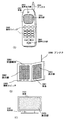
図18(A)は携帯電話であり、本体2901、音声出力部2902、音声入力部2903、表示部2904、操作スイッチ2905、アンテナ2906等を含む。本願発明を音声出力部2902、音声入力部2903、表示部2904やその他の信号制御回路に適用することができる。
【0195】
図18(B)は携帯書籍(電子書籍)であり、本体3001、表示部3002、3003、記憶媒体3004、操作スイッチ3005、アンテナ3006等を含む。本発明は表示部3002、3003やその他の信号回路に適用することができる。
【0196】
図18(C)はディスプレイであり、本体3101、支持台3102、表示部3103等を含む。本発明は表示部3103に適用することができる。本発明のディスプレイは特に大画面化した場合において有利であり、対角10インチ以上(特に30インチ以上)のディスプレイには有利である。
【0197】
以上の様に、本願発明の適用範囲は極めて広く、あらゆる分野の電子機器に適用することが可能である。また、本実施例の電子機器は実施例1〜7のどのような組み合わせからなる構成を用いても実現することができる。
【0198】
【発明の効果】
本願発明を用いることにより、AM−LCDに代表される電気光学装置において、同一基板上に移動度を優先するTFTと、オフ電流の小さいTFTとを機能に応じた回路に適用して、高い駆動能力と高い信頼性を有する電気光学装置を実現することが可能である。
【図面の簡単な説明】
【図1】AM−LCDの断面構造を示す図。
【図2】AM−LCDの作製工程を示す図。
【図3】AM−LCDの作製工程を示す図。
【図4】AM−LCDの作製工程を示す図。
【図5】AM−LCDの作製工程を示す図。
【図6】AM−LCD回路配置を示す図。
【図7】AM−LCDの作製工程を示す図。
【図8】AM−LCDの作製工程を示す図。
【図9】AM−LCDの作製工程を示す図。
【図10】AM−LCDの断面構造を示す図。
【図11】画素部の上面構造を示す図。
【図12】画素部の断面構造を示す図。
【図13】AM−LCDの外観を示す図。
【図14】ELパネル回路図。
【図15】ELパネル上面図及び断面図。
【図16】電子機器の一例を示す図。
【図17】電子機器の一例を示す図。
【図18】電子機器の一例を示す図。[0001]
BACKGROUND OF THE INVENTION
The present invention relates to a semiconductor device having a circuit composed of thin film transistors (hereinafter referred to as TFTs). For example, the present invention relates to an electro-optical device typified by a liquid crystal display panel and a configuration of an electronic apparatus in which such an electro-optical device is mounted as a component.
[0002]
Note that in this specification, a semiconductor device refers to all devices that can function by utilizing semiconductor characteristics, and an electro-optical device, a semiconductor circuit, and an electronic device are all semiconductor devices.
[0003]
[Prior art]
In recent years, a technique for forming a thin film transistor (TFT) using a semiconductor thin film (having a thickness of about several tens to several hundreds nm) formed on a substrate having an insulating surface has attracted attention.
Thin film transistors are widely applied to electronic devices such as ICs and electro-optical devices, and development of switching devices for image display devices is urgently required.
[0004]
For example, in a liquid crystal display device, a pixel unit that individually controls pixel areas arranged in a matrix, a driver circuit that controls the pixel unit (hereinafter referred to as a driver circuit), and a logic circuit that processes an external data signal Attempts have been made to apply TFTs to various electrical circuits such as processor circuits and memory circuits.
[0005]
A configuration (system on panel) in which these circuits (pixel portion, driver circuit, etc.) are integrated on a single substrate is known. In the pixel region, the pixel plays a role of holding the information sent from the driver circuit. If the off-state current of the TFT connected to the pixel is not sufficiently small, the information cannot be held, which is good. You cannot get a display.
[0006]
On the other hand, in a driver circuit, TFTs are required to have high mobility, and the higher the mobility, the simpler the circuit structure and the faster the display device can be operated.
[0007]
As described above, the characteristics required for the TFT to be arranged are different between the driver circuit and the pixel region. That is, the characteristics required for TFTs arranged in the pixel region are different.
That is, TFTs arranged in the pixel region are not required to have high mobility, but are required to have a small off-current and a uniform value in the pixel region. On the other hand, the mobility of the TFT of the driver circuit arranged in the periphery is given priority over the off current, and high mobility is required.
[0008]
However, it has been difficult to manufacture a TFT that prioritizes mobility and a TFT with a small off-current with high productivity without impairing reliability by using a conventional manufacturing method.
[0009]
[Problems to be solved by the invention]
As described above, in order to realize a system-on-panel including a driver circuit and a logic circuit, a completely new configuration that has not been conventionally required is required.
[0010]
The present invention answers such a requirement, and each circuit of an electro-optical device typified by AM-LCD is formed with a TFT having an appropriate structure according to the function, and has high reliability. It is an issue to provide.
[0011]
[Means for Solving the Problems]
The configuration of the invention disclosed in this specification is as follows.
In a semiconductor device having a driver circuit and a pixel portion formed over the same substrate,
The driver circuit and the pixel portion have an N-channel TFT including a channel formation region, a pair of high concentration impurity regions, and a low concentration impurity region,
The concentration of an element belonging to
The semiconductor device is characterized in that the concentration is higher than the concentration of an element belonging to
[0012]
In addition, the configuration of other inventions is as follows:
In a semiconductor device having a driver circuit and a pixel portion formed over the same substrate,
The driver circuit and the pixel portion have an N-channel TFT including a channel formation region, a pair of high concentration impurity regions, and a low concentration impurity region,
The concentration of an element belonging to
The semiconductor device is characterized in that the concentration is higher than the concentration of an element belonging to
[0013]
In addition, the configuration of other inventions is as follows:
In a semiconductor device having a driver circuit and a pixel portion formed over the same substrate,
The driver circuit and the pixel portion include a channel formation region, a gate insulating film formed in contact with the channel formation region, a gate electrode formed in contact with the gate insulating film, and the channel formation region interposed therebetween. An n-channel TFT having a pair of formed low-concentration impurity regions and a high-concentration impurity region formed in contact with the low-concentration impurity regions;
The low concentration impurity region of at least a part of the N-channel TFT included in the driver circuit overlaps the gate electrode through the gate insulating film,
In the semiconductor device, the low-concentration impurity region of at least a part of the N-channel TFT included in the pixel portion does not overlap with the gate electrode.
[0014]
In the above structure, the width in the channel length direction of the low-concentration impurity region of the N-channel TFT of the driver circuit is different from the width in the channel length direction of the low-concentration impurity region of the N-channel TFT in the pixel portion. It is characterized by that.
[0015]
In the above structure, the pixel portion is formed in contact with the shielding layer, an insulating film formed in contact with the shielding layer, a channel formation region formed in contact with the insulating film, and the channel formation region. A gate electrode formed in contact with the gate insulating film, a pair of low-concentration impurity regions formed across the channel formation region, and formed in contact with the low-concentration impurity region It has an N-channel TFT composed of a high concentration impurity region.
[0016]
In the above structure, the shielding layer overlaps the channel formation region and the low-concentration impurity region with the insulating film interposed therebetween.
[0017]
In the above structure, the width of the shielding layer in the channel length direction is wider than the width of the gate electrode in the channel length direction.
[0018]
The configuration of the invention for realizing the above structure is as follows.
A method for manufacturing a semiconductor device having a driver circuit and a pixel portion over the same substrate,
A first step of forming a shielding layer on the substrate;
A second step of forming an insulating film covering the shielding layer and the substrate;
A third step of forming a semiconductor layer on the insulating film;
A fourth step of crystallizing the semiconductor layer;
A fifth step of patterning the crystallized semiconductor layer to form an active layer of a driver circuit and an active layer of a pixel portion;
A sixth step of forming a gate insulating film on the active layer;
A seventh step of selectively adding an element belonging to Group 15 to the active layer of the driver circuit using a first mask;
An eighth step of forming wiring on the insulating film;
A ninth step of selectively adding an element belonging to Group 15 to the driver circuit and the active layer of the pixel portion using the wiring as a mask;
A tenth step of selectively adding an element belonging to Group 15 to the driver circuit and the active layer of the pixel portion using a second mask;
A method for manufacturing a semiconductor device.
[0019]
In the above structure, the concentration of the element belonging to Group 15 added in the seventh step is higher than the concentration of the element belonging to Group 15 added in the ninth step, and is added in the tenth step. It is characterized by being lower than the concentration of elements belonging to
[0020]
In addition, the configuration of other inventions is as follows:
A method for manufacturing a semiconductor device having a driver circuit and a pixel portion over the same substrate,
A first step of forming a shielding layer on the substrate;
A second step of forming an insulating film covering the shielding layer and the substrate;
A third step of forming a semiconductor layer on the insulating film;
A fourth step of crystallizing the semiconductor layer;
A fifth step of patterning the crystallized semiconductor layer to form an active layer of a driver circuit and an active layer of a pixel portion;
A sixth step of forming a gate insulating film on the active layer;
A seventh step of selectively adding an element belonging to Group 15 to the active layer of the driver circuit using a first mask;
An eighth step of performing a first treatment for activating an element belonging to Group 15 added to the active layer;
A ninth step of forming wiring on the insulating film;
A tenth step of selectively adding an element belonging to Group 15 to the driver circuit and the active layer of the pixel portion using the wiring as a mask;
An eleventh step of selectively adding an element belonging to Group 15 to the driver circuit and the active layer of the pixel portion using a second mask;
A twelfth step of performing a second treatment for activating the element belonging to Group 15 added to the active layer;
A method for manufacturing a semiconductor device.
[0021]
In the above structure, the shielding layer is formed only in a region to be a pixel portion.
[0022]
In the above structure, the second mask is formed by backside exposure.
[0023]
DETAILED DESCRIPTION OF THE INVENTION
An embodiment of the present invention will be described below with reference to FIG. FIG. 1 is a cross-sectional view of an AM-LCD in which a driver circuit and a pixel portion are integrally formed on the same substrate. Here, a CMOS circuit is shown as the basic circuit constituting the driver circuit, and a double gate TFT is shown as the pixel TFT. Of course, a triple gate structure or a single gate structure may be used.
[0024]
In FIG. 1,
[0025]
[0026]
[0027]
In FIG. 1, an active layer of a driver TFT includes a
[0028]
In addition, an active layer of a pixel TFT (here, NTFT is used) is formed of source or drain
[0029]
Note that in this specification, a structure having an LDD region to which a gate voltage is applied is referred to as a GOLD structure. On the other hand, a structure having only an LDD region to which no gate voltage is applied is called an LDD structure.
[0030]
In addition, in the present invention, an impurity is added at a concentration according to the function of each circuit in an electro-optical device typified by an AM-LCD formed on the same substrate, so that a low concentration impurity region of the TFT of each circuit is formed. It is characterized by forming.
[0031]
An element belonging to Group 15 with respect to the semiconductor layer is added to the
[0032]
On the other hand, an element belonging to
[0033]
Here, the
[0034]
As a material of the
[0035]
When the metal film is used as a material for the
[0036]
Next,
[0037]
Then, contact holes are provided in the first
[0038]
Here, the storage capacitor is formed of the transparent
[0039]
In addition, a shielding film using a material similar to that of the gate wiring may be provided on each TFT as necessary, or a structure in which a shielding film is provided on the counter substrate may be employed.
[0040]
As the second
[0041]
As the insulating film, an insulating film containing silicon as a main component or an oxide film of a shielding film is preferable. The insulating
[0042]
Further, as the
[0043]
In FIG. 1, the
[0044]
Although an example in which a shielding layer is formed only in the pixel portion is shown here, it is desirable to use a TFT with a small off-current for the sampling circuit in the driver circuit. It is desirable to form.
[0045]
The AM-LCD having the above-described structure is characterized in that it includes a driver circuit having a GOLD structure NTFT with high mobility and a pixel portion having an LDD structure NTFT with low off-current. In this manner, an electro-optical device having high driving ability and high reliability can be realized by applying a TFT that gives priority to mobility and a TFT having a small off-current to a circuit corresponding to the function on the same substrate. Is possible.
[0046]
The present invention having the above-described configuration will be described in more detail with the following examples.
[0047]
【Example】
[Example 1]
In this example, a manufacturing process for realizing the structure of FIG. 1 described in the “Embodiment Mode of the Invention” will be described. 2-5 is used for description.
[0048]
First, a light-transmitting
[0049]
As the
Moreover, you may laminate | stack combining these freely. Note that the shielding layer preferably has a tapered shape in order to prevent coverage failure due to a step.
[0050]
Next, a 200 nm thick silicon oxide film (also referred to as a base film) 201 and a 50 nm thick
[0051]
In this embodiment, an amorphous silicon film is used, but another semiconductor film may be used. A microcrystalline silicon (microcrystalline silicon) film or an amorphous silicon germanium film may be used. Further, as a method for forming the base film and the semiconductor film, a PCVD method, an LPCVD method, a sputtering method, or the like can be used.
[0052]
Next, the amorphous silicon film is crystallized. In the present invention, any known crystallization technique such as thermal crystallization, crystallization by irradiation with infrared light or ultraviolet light, thermal crystallization using a catalytic element, laser crystallization using a catalytic element, or the like is used. Good. In this example, the technique described in JP-A-9-31260 was used as the crystallization means.
The technique described in the publication uses an element selected from nickel, cobalt, palladium, germanium, platinum, iron, and copper as a catalyst element for promoting crystallization of a silicon film.
[0053]
First, a silicon oxide film is formed over an amorphous silicon film and patterned to form a
[0054]
Note that the active layer can be prevented from being contaminated with an organic substance by providing the
[0055]
Next, heat treatment at 500 to 650 ° C. is applied for 2 to 16 hours to perform gettering of the catalyst element (nickel in this embodiment) used for crystallization of the silicon film. In order to achieve the gettering action, a temperature of about ± 50 ° C. from the maximum temperature of the thermal history is necessary, but since the heat treatment for crystallization is performed at 550 to 600 ° C., the heat treatment at 500 to 650 ° C. is sufficient. The gettering action can be achieved. In this embodiment, nickel was moved in the direction of the arrow (shown in FIG. 2D) by applying a heat treatment at 600 ° C. for 8 hours, and was gettered and captured by phosphorus contained in the phosphorus-doped
[0056]
Next, after removing the
[0057]
Note that an impurity element (phosphorus or boron) for controlling the threshold voltage of the TFT may be added to the crystalline silicon film before and after forming the semiconductor layers of the driver TFT and the pixel TFT. This process may be performed only for NTFT or PTFT, or for both.
[0058]
Next, the
[0059]
After forming the
[0060]
In addition, the phosphorus addition step may use an ion implantation method in which mass separation is performed, or a plasma doping method in which mass separation is not performed. The practitioner may set optimum values for the acceleration voltage, the dose amount, and the like. In this embodiment, phosphine diluted with hydrogen to 1 to 10% is used as a doping gas, and the dose amount is 4 × 10. 13 atoms / cm 2 The acceleration voltage was 80 kV.
[0061]
Next, after removing the resist
[0062]
After completing the activation step in this way, a
[0063]
In this embodiment, as the
[0064]
Next, using the
[0065]
Similarly to the step shown in FIG. 3B, the phosphorus addition step may use an ion implantation method in which mass separation is performed, or a plasma doping method in which mass separation is not performed. The practitioner may set optimum values for the acceleration voltage, the dose amount, and the like.
[0066]
Next, a resist mask is formed by backside exposure. (FIG. 4A) At this time, in the pixel portion, the
[0067]
In this embodiment, the resist mask 217 is formed using backside exposure, but the resist mask 217 is not particularly limited, and a resist mask using a photomask may be used.
[0068]
Impurity doping is performed at a high concentration by using the resist
[0069]
Through this process, the
[0070]
In this manner, each impurity region is formed by adding an element belonging to Group 15 (phosphorus in this embodiment) in three steps.
[0071]
Thereafter, resist
[0072]
By this step, a
[0073]
Needless to say, the boron addition process may use an ion implantation method in which mass separation is performed, or a plasma doping method in which mass separation is not performed. The practitioner may set optimum values for the acceleration voltage, the dose amount, and the like.
[0074]
When all the impurity regions are thus formed, the resist
[0075]
Next, a first interlayer insulating film 249 is formed. In this embodiment, a 1 μm thick silicon oxide film formed by plasma CVD is used. Then, after forming contact holes, source wirings 230, 232, 233 and
[0076]
At this time, the
[0077]
Thereafter, a
[0078]
In this embodiment, it is effective to perform a plasma treatment using a gas containing hydrogen (ammonia gas in this embodiment) as a pretreatment for forming the silicon nitride film. Since hydrogen activated (excited) by the plasma by this pretreatment is confined in the active layer (semiconductor layer), hydrogen termination is effectively performed.
[0079]
Further, when a nitrous oxide gas is added in addition to a gas containing hydrogen, the surface of the object to be processed is cleaned by the generated moisture, and contamination by boron or the like contained in the atmosphere can be effectively prevented.
[0080]
When the
[0081]
Next, an acrylic film having a thickness of 1 μm is again formed as the third
The storage capacitor is formed by the
[0082]
As described above, in the present invention, impurities having different dose amounts are added three times or more to form the NTFT structure and the LDD region impurity concentration suitable for the function of each circuit, and an NTFT having a high mobility GOLD structure is formed. A feature is that a driver circuit including at least one or more and a pixel portion including an LDFT NTFT having a low off-state current are formed.
[0083]
FIG. 6 shows an example of the circuit configuration of the AM-LCD. The AM-LCD of this embodiment includes a source signal line side driver circuit 601, a gate signal line side driver circuit (A) 607, a gate signal line side driver circuit (B) 611, a precharge circuit 612, and a pixel portion 606. ing.
[0084]
The source signal line side driver circuit 601 includes a shift register circuit 602, a level shifter circuit 603, a buffer circuit 604, and a sampling circuit 605.
[0085]
The gate signal line driver circuit (A) 607 includes a
[0086]
Specifically, the NTFTs of the
[0087]
By adopting the configuration of this embodiment, a TFT that prioritizes mobility on the same substrate and a TFT with a small off-current are applied to a circuit corresponding to the function, and an electro-optic having high driving capability and high reliability The device could be realized.
[0088]
Although an example using a top gate type TFT is shown here, the present invention can be applied regardless of the TFT structure, and for example, can be applied to an inverted stagger type TFT.
[0089]
Further, according to the manufacturing process of this embodiment, the final active layer (semiconductor layer) of the TFT is formed of a crystalline silicon film having a unique crystal structure having continuity in the crystal lattice. The features will be described below.
[0090]
The active layer formed in accordance with the above manufacturing process has a crystal structure in which a plurality of needle-like or rod-like crystals (hereinafter abbreviated as rod-like crystals) are gathered and arranged microscopically. This was easily confirmed by observation with TEM (transmission electron microscopy).
[0091]
In addition, when electron diffraction and X-ray (X-ray) diffraction are used, the surface of the active layer (portion forming portion) has a {110} plane as a main orientation plane although the crystal axis includes some deviation. I was able to confirm that. As a result of detailed observation of an electron diffraction photograph with a spot diameter of about 1.5 μm by the present applicant, diffraction spots corresponding to the {110} plane appear clearly, but each spot has a distribution on a concentric circle. confirmed.
[0092]
In addition, the present applicant observed the grain boundaries formed by contact of individual rod-like crystals with HR-TEM (high resolution transmission electron microscopy), and confirmed that the crystal lattice has continuity at the grain boundaries. . This was easily confirmed because the observed lattice fringes were continuously connected at the grain boundaries.
[0093]
Note that the continuity of the crystal lattice at the crystal grain boundary results from the fact that the crystal grain boundary is a grain boundary called a “planar grain boundary”. The definition of the planar grain boundary in this specification is “Characterization of High-Efficiency Cast-Si Solar Cell Wafers by MBIC Measurement; Ryuichi Shimokawa and Yutaka Hayashi, Japanese Journal of Applied Physics vol.27, No.5, pp.751”. -758, 1988 ”is the“ Planar boundary ”.
[0094]
According to the above paper, planar grain boundaries include twin grain boundaries, special stacking faults, and special twist grain boundaries. This planar grain boundary is characterized by being electrically inactive. That is, although it is a crystal grain boundary, it does not function as a trap that inhibits the movement of carriers, and thus can be regarded as substantially nonexistent.
[0095]
In particular, when the crystal axis (axis perpendicular to the crystal plane) is the <110> axis, the {211} twin grain boundary is also called a corresponding grain boundary of Σ3. The Σ value is a parameter that serves as a guideline indicating the degree of consistency of the corresponding grain boundary. It is known that the smaller the Σ value, the better the grain boundary.
[0096]
As a result of observing the crystalline silicon film obtained by implementing the present embodiment in detail using TEM, most of the grain boundaries (90% or more, typically 95% or more) correspond to Σ3. It was found to be a grain boundary, that is, {211} twin grain boundary.
[0097]
In the crystal grain boundary formed between two crystal grains, when the plane orientation of both crystals is {110}, assuming that the angle formed by the lattice stripes corresponding to the {111} plane is θ, θ = 70.5 ° It is known that sometimes it becomes the corresponding grain boundary of Σ3.
[0098]
In the crystalline silicon film of this example, each lattice fringe of adjacent crystal grains in the crystal grain boundary is continuous at an angle of about 70.5 °. Therefore, this crystal grain boundary is a {211} twin crystal grain boundary. I came to the conclusion that there was.
[0099]
Incidentally, when θ = 38.9 °, the corresponding grain boundary of Σ9 is obtained, but such other crystal grain boundaries also existed.
[0100]
Such a corresponding grain boundary is formed only between crystal grains having the same plane orientation. That is, the crystalline silicon film obtained by carrying out the present embodiment can form such a corresponding grain boundary over a wide range because the plane orientation is approximately {110}.
[0101]
Such a crystal structure (exactly, the structure of the crystal grain boundary) indicates that two different crystal grains are joined with extremely good consistency at the crystal grain boundary. That is, the crystal lattice is continuously connected at the crystal grain boundary, and the trap level caused by crystal defects or the like is very difficult to create. Therefore, it can be considered that the semiconductor thin film having such a crystal structure is substantially free of crystal grain boundaries.
[0102]
Furthermore, it was confirmed by TEM observation that defects present in the crystal grains were almost disappeared by the heat treatment step (corresponding to the thermal oxidation step or gettering step in this embodiment) at a high temperature of 700 to 1150 ° C. ing. This is also clear from the fact that the number of defects is greatly reduced before and after this heat treatment step.
[0103]
The difference in the number of defects appears as a difference in spin density by electron spin resonance analysis (Electron Spin Resonance: ESR). At present, the spin density of the crystalline silicon film fabricated according to the fabrication process of this example is at least 5 × 10 17 spins / cm Three Below (preferably 3 × 10 17 spins / cm Three The following): However, since this measured value is close to the detection limit of existing measuring devices, the actual spin density is expected to be even lower.
[0104]
From the above, the crystalline silicon film obtained by carrying out this embodiment is considered to be a single crystal silicon film or a substantially single crystal silicon film because there are substantially no crystal grains and no crystal grain boundaries. Good.
[0105]
(Knowledge about electrical characteristics of TFT)
The TFT fabricated in this example showed electrical characteristics comparable to a MOSFET. The following data is obtained from the TFT manufactured by the present applicant (however, the thickness of the active layer is 30 nm and the thickness of the gate insulating film is 100 nm).
[0106]
(1) Sub-threshold coefficient, which is an indicator of switching performance (ON / OFF operation switching agility), is 60-100 mV / decade for both N-channel and P-channel TFTs (typically 60-85 mV / decade) And small.
(2) Field-effect mobility (μ FE ) 200-650cm for N-channel TFT 2 / Vs (typically 300-500cm 2 / Vs), 100-300cm with P-channel TFT 2 / Vs (typically 150-200cm 2 / Vs).
(3) Threshold voltage (V th ) Is as low as -0.5 to 1.5 V for N-channel TFTs and -1.5 to 0.5 V for P-channel TFTs.
[0107]
As described above, it has been confirmed that extremely excellent switching characteristics and high-speed operation characteristics can be realized.
[0108]
(Knowledge about circuit characteristics)
Next, frequency characteristics of a ring oscillator manufactured using a TFT formed by implementing this embodiment are shown. The ring oscillator is a circuit in which inverter circuits having a CMOS structure are connected in an odd-numbered ring shape, and is used to obtain a delay time per inverter circuit. The structure of the ring oscillator used in the experiment is as follows.
Number of stages: 9 stages
TFT gate insulating film thickness: 30nm and 50nm
TFT gate length (channel length): 0.6μm
[0109]
As a result of examining the oscillation frequency with this ring oscillator, it was possible to obtain an oscillation frequency of about 1 GHz at the maximum value. In addition, a shift register, which is actually one of the TEGs of the LSI circuit, was manufactured and the operating frequency was confirmed. As a result, an output pulse with an operating frequency of 100 MHz was obtained in a shift register circuit having a gate insulating film thickness of 30 nm, a gate length of 0.6 μm, a power supply voltage of 5 V, and the number of stages of 50.
[0110]
The amazing data of the ring oscillator and the shift register as described above indicate that the TFT of this embodiment has performance (electrical characteristics) comparable to or surpassing that of the MOSFET.
[0111]
[Example 2]
In this embodiment, the case where another means is used for forming the crystalline silicon film in Embodiment 1 will be described with reference to FIG.
[0112]
Specifically, a crystallization process (hereinafter referred to as laser crystallization) by irradiation with infrared light or ultraviolet light is used. Laser crystallization is effective because it can be processed in a short time with less stress on the substrate. Irradiation is performed using a pulsed laser using XeCl, ArF, KrF or the like as a laser gas, a continuous wave laser such as an Ar laser, or a continuous light emitting excimer laser. Laser crystallization conditions (laser beam shape, laser light wavelength, overlap rate, irradiation intensity, pulse width, repetition frequency, irradiation time, etc.) are implemented in consideration of the semiconductor film thickness, substrate temperature, etc. The person may determine appropriately.
[0113]
First, a silicon oxide film 702 was provided over a substrate 701, and an amorphous silicon film 703 was formed thereon. (FIG. 7A) Next, after a dehydrogenation step at 500 ° C. for 1 hour, a laser crystallization process was performed to form a crystalline silicon film 705. (Fig. 7 (B))
[0114]
The difference between this example and Example 1 is that laser crystallization is performed without using a catalyst element.
[0115]
If the subsequent steps are in accordance with Example 1, the structure of the TFT of the present invention can be obtained. However, although the catalyst element reduction process (gettering) is performed in the first embodiment, it is not particularly necessary in the present embodiment.
[0116]
Example 3
In this embodiment, the case where another means is used for forming the crystalline silicon film in Embodiment 1 will be described with reference to FIG. For simplification, only the driver circuit region is shown, and the shielding layer of the pixel portion is not shown.
[0117]
Specifically, the technique described in Japanese Patent Laid-Open No. 7-130652 (corresponding to US Patent No. 08 / 329,644) is used for crystallization of the amorphous silicon film. The technique described in the publication is a technique for performing crystallization by holding a catalyst element (typically nickel) for promoting crystallization on the surface of an amorphous silicon film.
[0118]
First, a silicon oxide film 802 was provided over a substrate 801, and an amorphous silicon film 803 was formed thereon. Further, a nickel acetate layer solution containing 10 ppm of nickel in terms of weight was applied to form a nickel-containing layer 804. (Fig. 8 (A))
[0119]
Next, after a dehydrogenation process at 500 ° C. for 1 hour, a heat treatment was performed at 500 to 650 ° C. for 4 to 12 hours to form a crystalline silicon film 805. (FIG. 8B) The crystalline silicon film 805 obtained in this way had very excellent crystallinity. In order to obtain the structure of the TFT of the present invention, the subsequent steps may be performed according to the first embodiment.
[0120]
In addition, the structure of a present Example can be freely combined with any structure of Examples 1-2.
[0121]
Example 4
In this embodiment, the case where another means is used for forming the crystalline silicon film and the gate insulating film in Embodiment 1 will be described with reference to FIG. For simplification, only the driver circuit region is shown, and the shielding layer of the pixel portion is not shown.
[0122]
Here, a substrate having heat resistance of at least about 700 to 1100 ° C. is necessary, and a quartz substrate 901 is used. Then, a crystalline semiconductor film was formed using the techniques shown in Examples 1 and 3, and semiconductor layers 902 and 903 were formed by patterning into an island shape in order to make this an active layer of the TFT. Then, a gate insulating film 904 was formed using a silicon oxide film as a main component so as to cover the semiconductor layers 902 and 903. In this embodiment, a silicon nitride oxide film is formed with a thickness of 70 nm by plasma CVD. (Fig. 9 (A))
[0123]
Then, heat treatment was performed in an atmosphere containing halogen (typically chlorine) and oxygen. In this example, the temperature was 950 ° C. for 30 minutes. The treatment temperature may be selected in the range of 700 to 1100 ° C., and the treatment time may be selected between 10 minutes and 8 hours.
[0124]
As a result, under the conditions of this example, a thermal oxide film was formed at the interface between the semiconductor layers 905 and 906 and the gate insulating film 904, and a gate insulating film 907 was formed. (FIG. 9B) In addition, in the process of oxidation in a halogen atmosphere, impurities contained in the gate insulating film 904 and the semiconductor layers 902 and 903, particularly a metal impurity element forms a compound with halogen, and enters the gas phase. Could be removed.
[0125]
The gate insulating film 907 manufactured through the above steps had high withstand voltage and a very good interface between the semiconductor layers 905 and 906 and the gate insulating film 907. In order to obtain the structure of the TFT of the present invention, the subsequent steps may be performed according to the first embodiment.
[0126]
In addition, the structure of a present Example can be freely combined with any structure of Examples 1-3.
[0127]
Example 5
In the present embodiment, a case will be described in which another means is used for reducing the catalytic element in the crystalline silicon film in the first embodiment.
[0128]
In Example 1, the phosphorus element is selectively added and then heat treatment is performed to perform the gettering for reducing the catalytic element in the crystalline silicon film. However, it goes without saying that the phosphorus element may be added to the entire surface. It is. In this embodiment, a method of gettering by bringing a liquid phase using high-temperature sulfuric acid into contact is shown.
[0129]
First, according to the process of Example 1, the state of FIG. Next, the entire substrate is immersed in a liquid phase heated to 300 ° C. (in this embodiment, in a sulfuric acid solution) to remove or reduce nickel used for crystallization. In addition, the method of making a sulfuric acid and a semiconductor layer contact is not specifically limited.
[0130]
In this way, the concentration of the catalyst element can be reduced in a short time by performing the catalyst element reduction process using the liquid phase. In order to obtain the structure of the TFT of the present invention, the subsequent steps may be performed according to the first embodiment.
[0131]
In addition, the structure of a present Example can be freely combined with any structure of Examples 1-4.
[0132]
Example 6
In this embodiment, an example in which a conductive shielding layer (also referred to as a black mask) 301 is used instead of the
[0133]
First, according to the first embodiment, a second interlayer insulating film is formed. Next, after a metal film containing titanium as a main component is formed by sputtering, patterning is performed to form a
[0134]
Next, a
[0135]
Then, in order to facilitate the formation of a contact between the pixel electrode and the drain electrode later, after the
[0136]
Finally, a
[0137]
With such a configuration, it is possible to form a sufficient storage capacitor and to prevent light degradation of the TFT.
[0138]
In this embodiment, a silicon oxide film formed by sputtering is used. However, if the black mask is oxidized by an oxidation method such as high pressure oxidation or anodization and the oxide film is used as a dielectric, the throughput is improved.
[0139]
In addition, the structure of a present Example can be freely combined with any structure of Examples 1-5.
[0140]
Example 7
In this embodiment, an example of a specific structure of the pixel portion (triple gate structure) is shown in FIG. The
[0141]
A cross-sectional view corresponding to FIG. 11 is shown in FIG. Further, the same reference numerals in FIG. 12 as those in FIG. 11 are used. Note that the transparent
[0142]
The present embodiment has only a triple gate structure, whereas the first embodiment has a double gate structure, and the basic structure is the same. Therefore, in order to obtain the structure of FIGS. 11 and 12, the manufacturing method shown in Embodiment 1 may be used.
[0143]
In addition, the structure of a present Example can be freely combined with any structure of Examples 1-6.
[0144]
Example 8
In this embodiment, a case will be described in which a TFT is formed on a substrate in the manufacturing process shown in Embodiment 1 and an AM-LCD is actually manufactured.
[0145]
When the state of FIG. 5C is obtained according to Embodiment 1, an alignment film is formed on the
[0146]
In addition, what is necessary is just to provide the spacer for maintaining a cell gap as needed.
Therefore, when the cell gap can be maintained without the spacer as in the AM-LCD having a diagonal of 1 inch or less, it is not particularly necessary.
[0147]
Next, the appearance of the AM-LCD manufactured as described above is shown in FIG. As shown in FIG. 13, the active matrix substrate and the counter substrate face each other, and liquid crystal is sandwiched between these substrates. The active matrix substrate includes a
[0148]
The scanning
[0149]
A scanning line is formed for each row of the
[0150]
The
[0151]
An
[0152]
In addition to the TN liquid crystal, various liquid crystals can be used for the liquid crystal display device manufactured according to the above embodiment. For example, 1998, SID, "Characteristics and Driving Scheme of Polymer-Stabilized Monostable FLCD Exhibiting Fast Response Time and High Contrast Ratio with Gray-Scale Capability" by H. Furue et al., 1997, SID DIGEST, 841, "A Full -Color Thresholdless Antiferroelectric LCD Exhibiting Wide Viewing Angle with Fast Response Time "by T. Yoshida et al., 1996, J. Mater. Chem. 6 (4), 671-673," Thresholdless antiferroelectricity in liquid crystals and its application to The liquid crystal disclosed in "displays" by S. Inui et al. or US Pat. No. 5,945,569 can be used.
[0153]
Further, in this embodiment, the liquid crystal display device is described as an example, but the present invention is applied to an EL (electroluminescence) display device and an EC (electrochromic) display device as long as it is an active matrix display device. It is also possible to do.
[0154]
In addition, a present Example can be freely combined with any Example of Examples 1-7.
[0155]
〔Example 9 ]
In this example, an example in which an EL (electroluminescence) display device is manufactured using the present invention will be described.
[0156]
FIG. 14 shows an example applied to an active matrix EL display.
[0157]
FIG. 14 is a circuit diagram of an active matrix EL display. Reference numeral 11 denotes a display area, and an X-direction peripheral driver circuit 12 and a Y-direction peripheral driver circuit 13 are provided around the display area. Each pixel in the display area 11 includes a switching
[0158]
In the active matrix EL display of this embodiment, the TFT structure used in the X-direction peripheral driver circuit 12 and the Y-direction peripheral driver circuit 13 is a GOLD structure, and the TFT structures of the
[0159]
FIG. 15A is a top view of an EL display device using the present invention. In FIG. 15A,
[0160]
At this time, a
[0161]
FIG. 15B shows a cross-sectional structure of the EL display device of this embodiment. A driver circuit TFT (here, an n-channel TFT and a p-channel TFT are combined on a
[0162]
The present invention can be used for the
[0163]
When the
[0164]
Next, an
[0165]
In this embodiment, the EL layer is formed by vapor deposition using a shadow mask. Color display is possible by forming a light emitting layer (a red light emitting layer, a green light emitting layer, and a blue light emitting layer) capable of emitting light having different wavelengths for each pixel using a shadow mask. In addition, there are a method in which a color conversion layer (CCM) and a color filter are combined, and a method in which a white light emitting layer and a color filter are combined, but either method may be used.
Needless to say, an EL display device emitting monochromatic light can also be used.
[0166]
After the
[0167]
In this embodiment, a stacked structure of a LiF (lithium fluoride) film and an Al (aluminum) film is used as the
[0168]
In order to electrically connect the
[0169]
A
[0170]
Further, a sealing material is provided inside the
[0171]
At this time, the
[0172]
In addition, a spacer may be included in the
[0173]
In the case where a spacer is provided, the
[0174]
As the
[0175]
However, the
[0176]
The
[0177]
In addition, a present Example can be freely combined with any Example of Examples 1-7.
[0178]
Example 10
The present invention can also be used when an interlayer insulating film is formed on a conventional MOSFET and a TFT is formed thereon. That is, it is also possible to realize a three-dimensional semiconductor device in which a reflective AM-LCD is formed on a semiconductor circuit.
[0179]
The semiconductor circuit may be formed on an SOI substrate such as SIMOX, Smart-Cut (registered trademark of SOITEC), ELTRAN (registered trademark of Canon Inc.), or the like.
[0180]
In addition, when implementing a present Example, you may combine any structure of Examples 1-8.
[0181]
Example 11
The CMOS circuit and the pixel portion formed by implementing the present invention can be used for various electro-optical devices (active matrix liquid crystal display, active matrix EL display, active matrix EC display). That is, the present invention can be implemented in all electronic devices in which these electro-optical devices are incorporated as display units.
[0182]
Such electronic devices include video cameras, digital cameras, projectors (rear or front type), head mounted displays (goggles type displays), car navigation systems, car stereos, personal computers, personal digital assistants (mobile computers, mobile phones) Or an electronic book). Examples of these are shown in FIGS. 16, 17 and 18.
[0183]
FIG. 16A illustrates a personal computer, which includes a main body 2001, an image input portion 2002, a display portion 2003, a
[0184]
FIG. 16B illustrates a video camera, which includes a main body 2101, a display portion 2102, an
[0185]
FIG. 16C illustrates a mobile computer, which includes a main body 2201, a
[0186]
FIG. 16D illustrates a goggle type display including a
[0187]
FIG. 16E shows a player using a recording medium (hereinafter referred to as a recording medium) on which a program is recorded, and includes a main body 2401, a
The present invention can be applied to the
[0188]
FIG. 16F illustrates a digital camera, which includes a main body 2501, a
[0189]
FIG. 17A illustrates a front projector, which includes a
[0190]
FIG. 17B shows a rear projector, which includes a
[0191]
Note that FIG. 17C is a diagram illustrating an example of the structure of the
[0192]
FIG. 17D illustrates an example of the structure of the light source
[0193]
However, the projector shown in FIG. 17 shows a case where a transmissive electro-optical device is used, and an application example in a reflective electro-optical device and an EL display device is not shown.
[0194]
FIG. 18A shows a cellular phone, which includes a
[0195]
FIG. 18B illustrates a portable book (electronic book) which includes a
[0196]
FIG. 18C illustrates a display, which includes a
[0197]
As described above, the application range of the present invention is extremely wide and can be applied to electronic devices in various fields. Moreover, the electronic apparatus of a present Example is realizable even if it uses the structure which consists of what combination of Examples 1-7.
[0198]
【The invention's effect】
By using the present invention, in an electro-optical device typified by an AM-LCD, a TFT that prioritizes mobility and a TFT with a small off-current are applied to a circuit corresponding to the function and driven at high speed. It is possible to realize an electro-optical device having high capability and high reliability.
[Brief description of the drawings]
FIG. 1 shows a cross-sectional structure of an AM-LCD.
FIGS. 2A to 2C are diagrams illustrating a manufacturing process of an AM-LCD. FIGS.
3A and 3B are diagrams illustrating a manufacturing process of an AM-LCD.
4A and 4B are diagrams illustrating a manufacturing process of an AM-LCD.
FIGS. 5A and 5B are diagrams illustrating a manufacturing process of an AM-LCD. FIGS.
FIG. 6 is a diagram showing an AM-LCD circuit arrangement.
7A and 7B are diagrams illustrating a manufacturing process of an AM-LCD.
FIGS. 8A and 8B are diagrams illustrating a manufacturing process of an AM-LCD. FIGS.
FIGS. 9A to 9C are diagrams illustrating a manufacturing process of an AM-LCD. FIGS.
FIG. 10 shows a cross-sectional structure of an AM-LCD.
FIG. 11 is a diagram showing a top structure of a pixel portion.
FIG. 12 illustrates a cross-sectional structure of a pixel portion.
FIG. 13 is a diagram illustrating an appearance of an AM-LCD.
FIG. 14 is an EL panel circuit diagram.
15A and 15B are a top view and a cross-sectional view of an EL panel.
FIG 16 illustrates an example of an electronic device.
FIG 17 illustrates an example of an electronic device.
FIG 18 illustrates an example of an electronic device.
Claims (10)
前記ドライバー回路及び前記画素部は下地膜上に設けられ、ゲート絶縁膜を有するNチャネル型TFTを有し、
前記Nチャネル型TFTの半導体層は、チャネル形成領域と、ソース領域及びドレイン領域と、LDD領域と、を有し、
前記ゲート絶縁膜上に接してゲート電極が設けられ、
前記ドライバー回路が有する前記ソース領域及びドレイン領域の15族に属する元素の濃度は、前記画素部が有する前記ソース領域及びドレイン領域の15族に属する元素の濃度よりも高く、
前記ドライバー回路が有するNチャネル型TFTの前記LDD領域は前記ゲート電極と一部が重なり、
前記画素部が有するNチャネル型TFTの前記LDD領域は前記ゲート電極と重ならないことを特徴とする半導体装置。A semiconductor device in which a driver circuit and a pixel portion are provided on the same substrate,
The driver circuit and the pixel portion is provided over the base film has a N-channel type TFT having a gate insulating film,
The semiconductor layer of the N-channel TFT has a channel formation region, a source region and a drain region, and an LDD region,
Is Gate electrodes provided in contact on the gate insulating film,
The concentration of the element belonging to Group 15 of the source region and drain region of the driver circuit is higher than the concentration of the element belonging to Group 15 of the source region and drain region of the pixel portion,
The LDD region of the N-channel TFT included in the driver circuit partially overlaps the gate electrode,
The semiconductor device, wherein the LDD region of the N-channel TFT included in the pixel portion does not overlap with the gate electrode.
前記ドライバー回路及び前記画素部は下地膜上に設けられ、ゲート絶縁膜を有するNチャネル型TFTを有し、
前記Nチャネル型TFTの半導体層は、チャネル形成領域と、ソース領域及びドレイン領域と、LDD領域と、を有し、
前記ゲート絶縁膜上に接してゲート電極が設けられ、
前記ドライバー回路が有する前記LDD領域の15族に属する元素の濃度は、前記画素部が有する前記LDD領域の15族に属する元素の濃度よりも高く、
前記ドライバー回路が有するNチャネル型TFTの前記LDD領域は前記ゲート電極と一部が重なり、
前記画素部が有するNチャネル型TFTの前記LDD領域は前記ゲート電極と重ならないことを特徴とする半導体装置。A semiconductor device in which a driver circuit and a pixel portion are provided on the same substrate,
The driver circuit and the pixel portion is provided over the base film has a N-channel type TFT having a gate insulating film,
The semiconductor layer of the N-channel TFT has a channel formation region, a source region and a drain region, and an LDD region,
Is Gate electrodes provided in contact on the gate insulating film,
The concentration of the element belonging to Group 15 of the LDD region of the driver circuit is higher than the concentration of the element belonging to Group 15 of the LDD region of the pixel portion,
The LDD region of the N-channel TFT included in the driver circuit partially overlaps the gate electrode,
The semiconductor device, wherein the LDD region of the N-channel TFT included in the pixel portion does not overlap with the gate electrode.
前記ドライバー回路及び前記画素部は下地膜上に設けられ、ゲート絶縁膜を有するNチャネル型TFTを有し、
前記Nチャネル型TFTの半導体層は、チャネル形成領域と、ソース領域及びドレイン領域と、LDD領域と、を有し、
前記ゲート絶縁膜上に接してゲート電極が設けられ、
前記ドライバー回路が有する前記LDD領域の15族に属する元素の濃度は、前記画素部が有する前記LDD領域の15族に属する元素の濃度よりも高く、且つ前記ドライバー回路が有する前記ソース領域及びドレイン領域の15族に属する元素の濃度は、前記画素部が有する前記ソース領域及びドレイン領域の15族に属する元素の濃度よりも高く、
前記ドライバー回路が有するNチャネル型TFTの前記LDD領域は前記ゲート電極と一部が重なり、
前記画素部が有するNチャネル型TFTの前記LDD領域は前記ゲート電極と重ならないことを特徴とする半導体装置。A semiconductor device in which a driver circuit and a pixel portion are provided on the same substrate,
The driver circuit and the pixel portion is provided over the base film has a N-channel type TFT having a gate insulating film,
The semiconductor layer of the N-channel TFT has a channel formation region, a source region and a drain region, and an LDD region,
Is Gate electrodes provided in contact on the gate insulating film,
The concentration of an element belonging to Group 15 of the LDD region included in the driver circuit is higher than the concentration of an element belonging to Group 15 of the LDD region included in the pixel portion, and the source region and the drain region included in the driver circuit. The concentration of the element belonging to Group 15 of the pixel region is higher than the concentration of the element belonging to Group 15 of the source region and drain region of the pixel portion,
The LDD region of the N-channel TFT included in the driver circuit partially overlaps the gate electrode,
The semiconductor device, wherein the LDD region of the N-channel TFT included in the pixel portion does not overlap with the gate electrode.
前記画素部が有する前記チャネル形成領域下に、前記下地膜を介して遮蔽層を有することを特徴とする半導体装置。In any one of Claims 1 thru | or 3 ,
A semiconductor device having a shielding layer under the channel formation region of the pixel portion with the base film interposed therebetween.
前記遮蔽層のチャネル長方向の幅は、前記画素部が有するNチャネル型TFTのゲート電極のチャネル長方向の幅よりも広いことを特徴とする半導体装置。In claim 4 ,
The width of the shielding layer in the channel length direction is wider than the width in the channel length direction of the gate electrode of the N-channel TFT included in the pixel portion.
基板上に下地膜を形成し、
前記下地膜上に非晶質半導体膜を形成し、
前記非晶質半導体膜を結晶化して結晶質半導体膜を形成し、
前記結晶質半導体膜をパターニングして半導体層を形成し、
前記半導体層上にゲート絶縁膜を形成し、
前記ゲート絶縁膜上に第1のマスクを形成し、
前記第1のマスクを用いて前記ドライバー回路が有する半導体層に対して15族に属する元素を選択的に添加することで前記ドライバー回路の半導体層のチャネル形成領域となる部分以外の領域に低濃度不純物領域を形成し、
前記第1のマスクを除去し、
前記ゲート絶縁膜上に導電層を前記ドライバー回路が有する前記低濃度不純物領域の一部及びチャネル形成領域となる部分と重畳させて、且つ前記画素部が有するチャネル形成領域となる部分と重畳させて形成し、
前記導電層をマスクとして用いて前記ドライバー回路及び前記画素部の半導体層に対して15族に属する元素を選択的に添加することで前記画素部の半導体層に低濃度不純物領域を形成し、
前記ドライバー回路が有する導電層には前記ドライバー回路が有する導電層上面と接し、且つ前記画素部が有する導電層には前記画素部が有する導電層を覆うようにして第2のマスクを形成し、
前記第2のマスクを用いて前記ドライバー回路及び前記画素部の半導体層に対して15族に属する元素を選択的に添加することで前記ドライバー回路及び前記画素部の半導体層にソース領域及びドレイン領域とLDD領域を形成し、
前記第2のマスクを除去し、
前記ドライバー回路が有する前記LDD領域の15族に属する元素の濃度は、前記画素部が有する前記LDD領域の15族に属する元素の濃度よりも高く、且つ前記ドライバー回路が有する前記ソース領域及びドレイン領域の15族に属する元素の濃度は、前記画素部が有する前記ソース領域及びドレイン領域の15族に属する元素の濃度よりも高いことを特徴とする半導体装置の作製方法。A method for manufacturing a semiconductor device having a driver circuit and a pixel portion over the same substrate,
Form a base film on the substrate,
Forming an amorphous semiconductor film on the base film;
Crystallizing the amorphous semiconductor film to form a crystalline semiconductor film,
Patterning the crystalline semiconductor film to form a semiconductor layer;
Forming a gate insulating film on the semiconductor layer;
Forming a first mask on the gate insulating film;
By selectively adding an element belonging to Group 15 to the semiconductor layer included in the driver circuit using the first mask, a low concentration is applied to a region other than a channel formation region of the semiconductor layer of the driver circuit. Forming impurity regions;
Removing the first mask;
Over the gate insulating film, a conductive layer is overlapped with a part of the low-concentration impurity region and a portion that forms a channel formation region of the driver circuit, and is overlapped with a portion that becomes a channel formation region of the pixel portion. Forming,
A low concentration impurity region is formed in the semiconductor layer of the pixel portion by selectively adding an element belonging to Group 15 to the driver circuit and the semiconductor layer of the pixel portion using the conductive layer as a mask,
Forming a second mask so that the conductive layer of the driver circuit is in contact with the upper surface of the conductive layer of the driver circuit, and the conductive layer of the pixel portion covers the conductive layer of the pixel portion;
A source region and a drain region are added to the driver circuit and the semiconductor layer of the pixel portion by selectively adding an element belonging to Group 15 to the driver circuit and the semiconductor layer of the pixel portion using the second mask. And forming an LDD region,
Removing the second mask;
The concentration of an element belonging to Group 15 of the LDD region included in the driver circuit is higher than the concentration of an element belonging to Group 15 of the LDD region included in the pixel portion, and the source region and the drain region included in the driver circuit. The concentration of an element belonging to Group 15 of the semiconductor device is higher than the concentration of an element belonging to Group 15 of the source region and drain region of the pixel portion.
基板上の画素部に遮蔽層を選択的に形成し、
前記基板及び前記遮蔽層上に下地膜を形成し、
前記下地膜上に非晶質半導体膜を形成し、
前記非晶質半導体膜を結晶化して結晶質半導体膜を形成し、
前記結晶質半導体膜をパターニングして半導体層を形成し、
前記半導体層上にゲート絶縁膜を形成し、
前記ゲート絶縁膜上に第1のマスクを形成し、
前記第1のマスクを用いて前記ドライバー回路が有する半導体層に対して15族に属する元素を選択的に添加することで前記ドライバー回路の半導体層のチャネル形成領域となる部分以外の領域に低濃度不純物領域を形成し、
前記第1のマスクを除去し、
前記ゲート絶縁膜上に導電層を前記ドライバー回路が有する前記低濃度不純物領域の一部及びチャネル形成領域となる部分と重畳させて、且つ前記画素部が有するチャネル形成領域となる部分と重畳させて形成し、
前記導電層をマスクとして用いて前記ドライバー回路及び前記画素部の半導体層に対して15族に属する元素を選択的に添加することで前記画素部の半導体層に低濃度不純物領域を形成し、
前記ドライバー回路が有する導電層には前記ドライバー回路が有する導電層上面と接し、且つ前記画素部が有する導電層には前記画素部が有する導電層を覆うようにして第2のマスクを形成し、
前記第2のマスクを用いて前記ドライバー回路及び前記画素部の半導体層に対して15族に属する元素を選択的に添加することで前記ドライバー回路及び前記画素部の半導体層にソース領域及びドレイン領域とLDD領域を形成し、
前記第2のマスクを除去し、
前記ドライバー回路が有する前記LDD領域の15族に属する元素の濃度は、前記画素部が有する前記LDD領域の15族に属する元素の濃度よりも高く、且つ前記ドライバー回路が有する前記ソース領域及びドレイン領域の15族に属する元素の濃度は、前記画素部が有する前記ソース領域及びドレイン領域の15族に属する元素の濃度よりも高いことを特徴とする半導体装置の作製方法。A method for manufacturing a semiconductor device having a driver circuit and a pixel portion over the same substrate,
Selectively forming a shielding layer on the pixel portion on the substrate;
Forming a base film on the substrate and the shielding layer;
Forming an amorphous semiconductor film on the base film;
Crystallizing the amorphous semiconductor film to form a crystalline semiconductor film,
Patterning the crystalline semiconductor film to form a semiconductor layer;
Forming a gate insulating film on the semiconductor layer;
Forming a first mask on the gate insulating film;
By selectively adding an element belonging to Group 15 to the semiconductor layer included in the driver circuit using the first mask, a low concentration is applied to a region other than a channel formation region of the semiconductor layer of the driver circuit. Forming impurity regions;
Removing the first mask;
Over the gate insulating film, a conductive layer is overlapped with a part of the low-concentration impurity region and a portion that forms a channel formation region of the driver circuit, and is overlapped with a portion that becomes a channel formation region of the pixel portion. Forming,
A low concentration impurity region is formed in the semiconductor layer of the pixel portion by selectively adding an element belonging to Group 15 to the driver circuit and the semiconductor layer of the pixel portion using the conductive layer as a mask,
Forming a second mask so that the conductive layer of the driver circuit is in contact with the upper surface of the conductive layer of the driver circuit, and the conductive layer of the pixel portion covers the conductive layer of the pixel portion;
A source region and a drain region are added to the driver circuit and the semiconductor layer of the pixel portion by selectively adding an element belonging to Group 15 to the driver circuit and the semiconductor layer of the pixel portion using the second mask. And forming an LDD region,
Removing the second mask;
The concentration of an element belonging to Group 15 of the LDD region included in the driver circuit is higher than the concentration of an element belonging to Group 15 of the LDD region included in the pixel portion, and the source region and the drain region included in the driver circuit. The concentration of an element belonging to Group 15 of the semiconductor device is higher than the concentration of an element belonging to Group 15 of the source region and drain region of the pixel portion.
基板上の画素部に遮蔽層を選択的に形成し、
前記基板及び前記遮蔽層上に下地膜を形成し、
前記下地膜上に非晶質半導体膜を形成し、
前記非晶質半導体膜を結晶化して結晶質半導体膜を形成し、
前記結晶質半導体膜をパターニングして半導体層を形成し、
前記半導体層上にゲート絶縁膜を形成し、
前記ゲート絶縁膜上に第1のマスクを形成し、
前記第1のマスクを用いて前記ドライバー回路が有する半導体層に対して15族に属する元素を選択的に添加することで前記ドライバー回路の半導体層のチャネル形成領域となる部分以外の領域に低濃度不純物領域を形成し、
前記第1のマスクを除去し、
前記ゲート絶縁膜上に導電層を前記ドライバー回路が有する前記低濃度不純物領域の一部及びチャネル形成領域となる部分と重畳させて、且つ前記画素部が有するチャネル形成領域となる部分と重畳させて形成し、
前記導電層をマスクとして用いて前記ドライバー回路及び前記画素部の半導体層に対して15族に属する元素を選択的に添加することで前記画素部の半導体層に低濃度不純物領域を形成し、
前記ドライバー回路が有する導電層には前記ドライバー回路が有する導電層上面と接し、且つ前記画素部が有する導電層には前記画素部が有する導電層を覆うようにして裏面露光により第2のマスクを形成し、
前記第2のマスクを用いて前記ドライバー回路及び前記画素部の半導体層に対して15族に属する元素を選択的に添加することで前記ドライバー回路及び前記画素部の半導体層にソース領域及びドレイン領域とLDD領域を形成し、
前記第2のマスクを除去し、
前記ドライバー回路が有する前記LDD領域の15族に属する元素の濃度は、前記画素部が有する前記LDD領域の15族に属する元素の濃度よりも高く、且つ前記ドライバー回路が有する前記ソース領域及びドレイン領域の15族に属する元素の濃度は、前記画素部が有する前記ソース領域及びドレイン領域の15族に属する元素の濃度よりも高いことを特徴とする半導体装置の作製方法。A method for manufacturing a semiconductor device having a driver circuit and a pixel portion over the same substrate,
Selectively forming a shielding layer on the pixel portion on the substrate;
Forming a base film on the substrate and the shielding layer;
Forming an amorphous semiconductor film on the base film;
Crystallizing the amorphous semiconductor film to form a crystalline semiconductor film,
Patterning the crystalline semiconductor film to form a semiconductor layer;
Forming a gate insulating film on the semiconductor layer;
Forming a first mask on the gate insulating film;
By selectively adding an element belonging to Group 15 to the semiconductor layer included in the driver circuit using the first mask, a low concentration is applied to a region other than a channel formation region of the semiconductor layer of the driver circuit. Forming impurity regions;
Removing the first mask;
Over the gate insulating film, a conductive layer is overlapped with a part of the low-concentration impurity region and a portion that forms a channel formation region of the driver circuit, and is overlapped with a portion that becomes a channel formation region of the pixel portion. Forming,
A low concentration impurity region is formed in the semiconductor layer of the pixel portion by selectively adding an element belonging to Group 15 to the driver circuit and the semiconductor layer of the pixel portion using the conductive layer as a mask,
The conductive layer of the driver circuit is in contact with the upper surface of the conductive layer of the driver circuit, and the conductive layer of the pixel portion is covered with a second mask by backside exposure so as to cover the conductive layer of the pixel portion. Forming,
A source region and a drain region are added to the driver circuit and the semiconductor layer of the pixel portion by selectively adding an element belonging to Group 15 to the driver circuit and the semiconductor layer of the pixel portion using the second mask. And forming an LDD region,
Removing the second mask;
The concentration of an element belonging to Group 15 of the LDD region included in the driver circuit is higher than the concentration of an element belonging to Group 15 of the LDD region included in the pixel portion, and the source region and the drain region included in the driver circuit. The concentration of an element belonging to Group 15 of the semiconductor device is higher than the concentration of an element belonging to Group 15 of the source region and drain region of the pixel portion.
Priority Applications (1)
| Application Number | Priority Date | Filing Date | Title |
|---|---|---|---|
| JP2000058493A JP4583540B2 (en) | 1999-03-04 | 2000-03-03 | Semiconductor device and manufacturing method thereof |
Applications Claiming Priority (3)
| Application Number | Priority Date | Filing Date | Title |
|---|---|---|---|
| JP11-57754 | 1999-03-04 | ||
| JP5775499 | 1999-03-04 | ||
| JP2000058493A JP4583540B2 (en) | 1999-03-04 | 2000-03-03 | Semiconductor device and manufacturing method thereof |
Publications (3)
| Publication Number | Publication Date |
|---|---|
| JP2000315798A JP2000315798A (en) | 2000-11-14 |
| JP2000315798A5 JP2000315798A5 (en) | 2007-04-26 |
| JP4583540B2 true JP4583540B2 (en) | 2010-11-17 |
Family
ID=26398826
Family Applications (1)
| Application Number | Title | Priority Date | Filing Date |
|---|---|---|---|
| JP2000058493A Expired - Fee Related JP4583540B2 (en) | 1999-03-04 | 2000-03-03 | Semiconductor device and manufacturing method thereof |
Country Status (1)
| Country | Link |
|---|---|
| JP (1) | JP4583540B2 (en) |
Families Citing this family (15)
| Publication number | Priority date | Publication date | Assignee | Title |
|---|---|---|---|---|
| US7821065B2 (en) | 1999-03-02 | 2010-10-26 | Semiconductor Energy Laboratory Co., Ltd. | Semiconductor device comprising a thin film transistor comprising a semiconductor thin film and method of manufacturing the same |
| JP2001175198A (en) | 1999-12-14 | 2001-06-29 | Semiconductor Energy Lab Co Ltd | Semiconductor device and manufacturing method therefor |
| US7525165B2 (en) | 2000-04-17 | 2009-04-28 | Semiconductor Energy Laboratory Co., Ltd. | Light emitting device and manufacturing method thereof |
| JP4739510B2 (en) * | 2000-12-15 | 2011-08-03 | 株式会社半導体エネルギー研究所 | Semiconductor device and manufacturing method thereof |
| JP4798907B2 (en) | 2001-09-26 | 2011-10-19 | 株式会社半導体エネルギー研究所 | Semiconductor device |
| JP2003209041A (en) * | 2002-01-15 | 2003-07-25 | Seiko Epson Corp | Measuring method of aligning accuracy of pattern, forming method of pattern, manufacturing method of electro-optical device and manufacturing method of semiconductor device |
| JP2003298069A (en) * | 2002-01-30 | 2003-10-17 | Sanyo Electric Co Ltd | Semiconductor display device, its manufacturing method, and active-matrix display device |
| TWI288443B (en) | 2002-05-17 | 2007-10-11 | Semiconductor Energy Lab | SiN film, semiconductor device, and the manufacturing method thereof |
| TWI247180B (en) | 2004-08-06 | 2006-01-11 | Au Optronics Corp | Thin film transistor structure for flat panel display and method for fabricating the same |
| CN100459157C (en) * | 2004-08-26 | 2009-02-04 | 友达光电股份有限公司 | Thin film transistor structure for plane display device and its producing method |
| KR100647691B1 (en) | 2005-04-22 | 2006-11-23 | 삼성에스디아이 주식회사 | Flat panel display apparatus |
| JP2007188936A (en) * | 2006-01-11 | 2007-07-26 | Epson Imaging Devices Corp | Display device |
| KR101291434B1 (en) | 2009-07-31 | 2013-08-07 | 가부시키가이샤 한도오따이 에네루기 켄큐쇼 | Semiconductor device and manufacturing method thereof |
| KR101746198B1 (en) | 2009-09-04 | 2017-06-12 | 가부시키가이샤 한도오따이 에네루기 켄큐쇼 | Display device and electronic device |
| JP5153921B2 (en) * | 2011-06-27 | 2013-02-27 | 株式会社半導体エネルギー研究所 | Display device and portable information terminal |
-
2000
- 2000-03-03 JP JP2000058493A patent/JP4583540B2/en not_active Expired - Fee Related
Also Published As
| Publication number | Publication date |
|---|---|
| JP2000315798A (en) | 2000-11-14 |
Similar Documents
| Publication | Publication Date | Title |
|---|---|---|
| JP6587713B2 (en) | Liquid crystal display | |
| US6674136B1 (en) | Semiconductor device having driver circuit and pixel section provided over same substrate | |
| JP5656335B2 (en) | Semiconductor device | |
| JP5298094B2 (en) | Semiconductor device and manufacturing method thereof | |
| US20120187837A1 (en) | Method for manufacturing an electrooptical device | |
| JP4583540B2 (en) | Semiconductor device and manufacturing method thereof | |
| JP4578609B2 (en) | Electro-optic device | |
| JP2000353809A (en) | Semiconductor device and manufacture thereof | |
| JP4860021B2 (en) | Method for manufacturing semiconductor device | |
| JP4540776B2 (en) | Semiconductor device and electronic equipment | |
| JP4850763B2 (en) | Method for manufacturing semiconductor device | |
| JP4641586B2 (en) | Method for manufacturing semiconductor device | |
| JP4700159B2 (en) | Method for manufacturing semiconductor device | |
| JP2000243974A (en) | Semiconductor device and manufacture thereof |
Legal Events
| Date | Code | Title | Description |
|---|---|---|---|
| A521 | Written amendment |
Free format text: JAPANESE INTERMEDIATE CODE: A523 Effective date: 20070301 |
|
| A621 | Written request for application examination |
Free format text: JAPANESE INTERMEDIATE CODE: A621 Effective date: 20070301 |
|
| A977 | Report on retrieval |
Free format text: JAPANESE INTERMEDIATE CODE: A971007 Effective date: 20100518 |
|
| A131 | Notification of reasons for refusal |
Free format text: JAPANESE INTERMEDIATE CODE: A131 Effective date: 20100615 |
|
| A521 | Written amendment |
Free format text: JAPANESE INTERMEDIATE CODE: A523 Effective date: 20100806 |
|
| TRDD | Decision of grant or rejection written | ||
| A01 | Written decision to grant a patent or to grant a registration (utility model) |
Free format text: JAPANESE INTERMEDIATE CODE: A01 Effective date: 20100831 |
|
| A01 | Written decision to grant a patent or to grant a registration (utility model) |
Free format text: JAPANESE INTERMEDIATE CODE: A01 |
|
| A61 | First payment of annual fees (during grant procedure) |
Free format text: JAPANESE INTERMEDIATE CODE: A61 Effective date: 20100901 |
|
| R150 | Certificate of patent or registration of utility model |
Ref document number: 4583540 Country of ref document: JP Free format text: JAPANESE INTERMEDIATE CODE: R150 Free format text: JAPANESE INTERMEDIATE CODE: R150 |
|
| FPAY | Renewal fee payment (event date is renewal date of database) |
Free format text: PAYMENT UNTIL: 20130910 Year of fee payment: 3 |
|
| FPAY | Renewal fee payment (event date is renewal date of database) |
Free format text: PAYMENT UNTIL: 20130910 Year of fee payment: 3 |
|
| R250 | Receipt of annual fees |
Free format text: JAPANESE INTERMEDIATE CODE: R250 |
|
| R250 | Receipt of annual fees |
Free format text: JAPANESE INTERMEDIATE CODE: R250 |
|
| R250 | Receipt of annual fees |
Free format text: JAPANESE INTERMEDIATE CODE: R250 |
|
| R250 | Receipt of annual fees |
Free format text: JAPANESE INTERMEDIATE CODE: R250 |
|
| R250 | Receipt of annual fees |
Free format text: JAPANESE INTERMEDIATE CODE: R250 |
|
| R250 | Receipt of annual fees |
Free format text: JAPANESE INTERMEDIATE CODE: R250 |
|
| LAPS | Cancellation because of no payment of annual fees |