JP4627843B2 - Semiconductor device - Google Patents
Semiconductor device Download PDFInfo
- Publication number
- JP4627843B2 JP4627843B2 JP2000219727A JP2000219727A JP4627843B2 JP 4627843 B2 JP4627843 B2 JP 4627843B2 JP 2000219727 A JP2000219727 A JP 2000219727A JP 2000219727 A JP2000219727 A JP 2000219727A JP 4627843 B2 JP4627843 B2 JP 4627843B2
- Authority
- JP
- Japan
- Prior art keywords
- film
- substrate
- wiring
- circuit
- tft
- Prior art date
- Legal status (The legal status is an assumption and is not a legal conclusion. Google has not performed a legal analysis and makes no representation as to the accuracy of the status listed.)
- Expired - Fee Related
Links
- 239000004065 semiconductor Substances 0.000 title claims description 83
- 239000010408 film Substances 0.000 claims description 440
- 239000000758 substrate Substances 0.000 claims description 122
- 238000000034 method Methods 0.000 claims description 71
- 229910052751 metal Inorganic materials 0.000 claims description 50
- 239000002184 metal Substances 0.000 claims description 50
- 230000001681 protective effect Effects 0.000 claims description 41
- 125000006850 spacer group Chemical group 0.000 claims description 34
- 239000000463 material Substances 0.000 claims description 28
- 230000008569 process Effects 0.000 claims description 20
- 239000010409 thin film Substances 0.000 claims description 12
- 239000011810 insulating material Substances 0.000 claims description 6
- 238000005530 etching Methods 0.000 description 62
- 239000012535 impurity Substances 0.000 description 59
- 239000011159 matrix material Substances 0.000 description 46
- XUIMIQQOPSSXEZ-UHFFFAOYSA-N Silicon Chemical compound [Si] XUIMIQQOPSSXEZ-UHFFFAOYSA-N 0.000 description 44
- 229910052710 silicon Inorganic materials 0.000 description 44
- 239000010703 silicon Substances 0.000 description 44
- 239000007789 gas Substances 0.000 description 37
- 239000004973 liquid crystal related substance Substances 0.000 description 32
- 238000004519 manufacturing process Methods 0.000 description 28
- 239000010410 layer Substances 0.000 description 27
- 238000009616 inductively coupled plasma Methods 0.000 description 19
- 230000003287 optical effect Effects 0.000 description 18
- OAICVXFJPJFONN-UHFFFAOYSA-N Phosphorus Chemical compound [P] OAICVXFJPJFONN-UHFFFAOYSA-N 0.000 description 17
- 229910052698 phosphorus Inorganic materials 0.000 description 17
- 239000011574 phosphorus Substances 0.000 description 17
- 238000012545 processing Methods 0.000 description 17
- 239000003990 capacitor Substances 0.000 description 15
- 230000015572 biosynthetic process Effects 0.000 description 14
- 239000011521 glass Substances 0.000 description 14
- 238000005268 plasma chemical vapour deposition Methods 0.000 description 14
- 229910045601 alloy Inorganic materials 0.000 description 13
- 239000000956 alloy Substances 0.000 description 13
- XLOMVQKBTHCTTD-UHFFFAOYSA-N zinc oxide Inorganic materials [Zn]=O XLOMVQKBTHCTTD-UHFFFAOYSA-N 0.000 description 13
- 125000004429 atom Chemical group 0.000 description 12
- 229910052739 hydrogen Inorganic materials 0.000 description 12
- 238000004544 sputter deposition Methods 0.000 description 12
- 238000006243 chemical reaction Methods 0.000 description 11
- 150000002500 ions Chemical class 0.000 description 11
- 239000011347 resin Substances 0.000 description 11
- 229920005989 resin Polymers 0.000 description 11
- 239000010936 titanium Substances 0.000 description 11
- ZOXJGFHDIHLPTG-UHFFFAOYSA-N Boron Chemical compound [B] ZOXJGFHDIHLPTG-UHFFFAOYSA-N 0.000 description 10
- 229910052796 boron Inorganic materials 0.000 description 10
- 239000000460 chlorine Substances 0.000 description 10
- 239000001257 hydrogen Substances 0.000 description 10
- UFHFLCQGNIYNRP-UHFFFAOYSA-N Hydrogen Chemical compound [H][H] UFHFLCQGNIYNRP-UHFFFAOYSA-N 0.000 description 9
- 238000001312 dry etching Methods 0.000 description 9
- 239000011229 interlayer Substances 0.000 description 9
- MZLGASXMSKOWSE-UHFFFAOYSA-N tantalum nitride Chemical compound [Ta]#N MZLGASXMSKOWSE-UHFFFAOYSA-N 0.000 description 9
- 229910052782 aluminium Inorganic materials 0.000 description 8
- 239000002585 base Substances 0.000 description 8
- 238000010586 diagram Methods 0.000 description 8
- 238000010438 heat treatment Methods 0.000 description 8
- 229910052760 oxygen Inorganic materials 0.000 description 8
- VYPSYNLAJGMNEJ-UHFFFAOYSA-N silicon dioxide Inorganic materials O=[Si]=O VYPSYNLAJGMNEJ-UHFFFAOYSA-N 0.000 description 8
- XAGFODPZIPBFFR-UHFFFAOYSA-N aluminium Chemical compound [Al] XAGFODPZIPBFFR-UHFFFAOYSA-N 0.000 description 7
- 230000006870 function Effects 0.000 description 7
- 238000005224 laser annealing Methods 0.000 description 7
- 239000012071 phase Substances 0.000 description 7
- 239000000565 sealant Substances 0.000 description 7
- WFKWXMTUELFFGS-UHFFFAOYSA-N tungsten Chemical compound [W] WFKWXMTUELFFGS-UHFFFAOYSA-N 0.000 description 7
- 229910052721 tungsten Inorganic materials 0.000 description 7
- 239000010937 tungsten Substances 0.000 description 7
- 239000011787 zinc oxide Substances 0.000 description 7
- 238000000137 annealing Methods 0.000 description 6
- 238000005984 hydrogenation reaction Methods 0.000 description 6
- 230000001965 increasing effect Effects 0.000 description 6
- 229920001721 polyimide Polymers 0.000 description 6
- 229910052814 silicon oxide Inorganic materials 0.000 description 6
- 238000003860 storage Methods 0.000 description 6
- IJGRMHOSHXDMSA-UHFFFAOYSA-N Atomic nitrogen Chemical compound N#N IJGRMHOSHXDMSA-UHFFFAOYSA-N 0.000 description 5
- 239000004642 Polyimide Substances 0.000 description 5
- 229910052581 Si3N4 Inorganic materials 0.000 description 5
- 230000004913 activation Effects 0.000 description 5
- 239000000853 adhesive Substances 0.000 description 5
- 230000001070 adhesive effect Effects 0.000 description 5
- 229910021417 amorphous silicon Inorganic materials 0.000 description 5
- 239000012298 atmosphere Substances 0.000 description 5
- 229910021419 crystalline silicon Inorganic materials 0.000 description 5
- 238000002425 crystallisation Methods 0.000 description 5
- 230000005684 electric field Effects 0.000 description 5
- 238000005401 electroluminescence Methods 0.000 description 5
- 238000005070 sampling Methods 0.000 description 5
- HQVNEWCFYHHQES-UHFFFAOYSA-N silicon nitride Chemical compound N12[Si]34N5[Si]62N3[Si]51N64 HQVNEWCFYHHQES-UHFFFAOYSA-N 0.000 description 5
- XKRFYHLGVUSROY-UHFFFAOYSA-N Argon Chemical compound [Ar] XKRFYHLGVUSROY-UHFFFAOYSA-N 0.000 description 4
- VEXZGXHMUGYJMC-UHFFFAOYSA-N Hydrochloric acid Chemical compound Cl VEXZGXHMUGYJMC-UHFFFAOYSA-N 0.000 description 4
- NRTOMJZYCJJWKI-UHFFFAOYSA-N Titanium nitride Chemical compound [Ti]#N NRTOMJZYCJJWKI-UHFFFAOYSA-N 0.000 description 4
- 230000001133 acceleration Effects 0.000 description 4
- QVGXLLKOCUKJST-UHFFFAOYSA-N atomic oxygen Chemical compound [O] QVGXLLKOCUKJST-UHFFFAOYSA-N 0.000 description 4
- 230000008859 change Effects 0.000 description 4
- 230000008025 crystallization Effects 0.000 description 4
- 239000001301 oxygen Substances 0.000 description 4
- 239000002245 particle Substances 0.000 description 4
- 239000002356 single layer Substances 0.000 description 4
- 229910052719 titanium Inorganic materials 0.000 description 4
- OYQCBJZGELKKPM-UHFFFAOYSA-N zinc indium(3+) oxygen(2-) Chemical compound [O-2].[Zn+2].[O-2].[In+3] OYQCBJZGELKKPM-UHFFFAOYSA-N 0.000 description 4
- GYHNNYVSQQEPJS-UHFFFAOYSA-N Gallium Chemical compound [Ga] GYHNNYVSQQEPJS-UHFFFAOYSA-N 0.000 description 3
- RTAQQCXQSZGOHL-UHFFFAOYSA-N Titanium Chemical compound [Ti] RTAQQCXQSZGOHL-UHFFFAOYSA-N 0.000 description 3
- 229910001080 W alloy Inorganic materials 0.000 description 3
- NIXOWILDQLNWCW-UHFFFAOYSA-N acrylic acid group Chemical group C(C=C)(=O)O NIXOWILDQLNWCW-UHFFFAOYSA-N 0.000 description 3
- IVHJCRXBQPGLOV-UHFFFAOYSA-N azanylidynetungsten Chemical compound [W]#N IVHJCRXBQPGLOV-UHFFFAOYSA-N 0.000 description 3
- 238000004891 communication Methods 0.000 description 3
- 239000004020 conductor Substances 0.000 description 3
- 230000007797 corrosion Effects 0.000 description 3
- 238000005260 corrosion Methods 0.000 description 3
- 238000011161 development Methods 0.000 description 3
- ZOCHARZZJNPSEU-UHFFFAOYSA-N diboron Chemical compound B#B ZOCHARZZJNPSEU-UHFFFAOYSA-N 0.000 description 3
- 230000000694 effects Effects 0.000 description 3
- 229910052733 gallium Inorganic materials 0.000 description 3
- 230000010355 oscillation Effects 0.000 description 3
- 238000000206 photolithography Methods 0.000 description 3
- 239000004033 plastic Substances 0.000 description 3
- 229920003023 plastic Polymers 0.000 description 3
- 239000012495 reaction gas Substances 0.000 description 3
- 229910052715 tantalum Inorganic materials 0.000 description 3
- GUVRBAGPIYLISA-UHFFFAOYSA-N tantalum atom Chemical compound [Ta] GUVRBAGPIYLISA-UHFFFAOYSA-N 0.000 description 3
- ZAMOUSCENKQFHK-UHFFFAOYSA-N Chlorine atom Chemical compound [Cl] ZAMOUSCENKQFHK-UHFFFAOYSA-N 0.000 description 2
- RYGMFSIKBFXOCR-UHFFFAOYSA-N Copper Chemical compound [Cu] RYGMFSIKBFXOCR-UHFFFAOYSA-N 0.000 description 2
- PXGOKWXKJXAPGV-UHFFFAOYSA-N Fluorine Chemical compound FF PXGOKWXKJXAPGV-UHFFFAOYSA-N 0.000 description 2
- ZOKXTWBITQBERF-UHFFFAOYSA-N Molybdenum Chemical compound [Mo] ZOKXTWBITQBERF-UHFFFAOYSA-N 0.000 description 2
- XYFCBTPGUUZFHI-UHFFFAOYSA-N Phosphine Chemical compound P XYFCBTPGUUZFHI-UHFFFAOYSA-N 0.000 description 2
- 229910006404 SnO 2 Inorganic materials 0.000 description 2
- 229910001362 Ta alloys Inorganic materials 0.000 description 2
- BOTDANWDWHJENH-UHFFFAOYSA-N Tetraethyl orthosilicate Chemical compound CCO[Si](OCC)(OCC)OCC BOTDANWDWHJENH-UHFFFAOYSA-N 0.000 description 2
- 230000003213 activating effect Effects 0.000 description 2
- 229910052783 alkali metal Inorganic materials 0.000 description 2
- 150000001340 alkali metals Chemical class 0.000 description 2
- 229910052786 argon Inorganic materials 0.000 description 2
- GPBUGPUPKAGMDK-UHFFFAOYSA-N azanylidynemolybdenum Chemical compound [Mo]#N GPBUGPUPKAGMDK-UHFFFAOYSA-N 0.000 description 2
- UMIVXZPTRXBADB-UHFFFAOYSA-N benzocyclobutene Chemical compound C1=CC=C2CCC2=C1 UMIVXZPTRXBADB-UHFFFAOYSA-N 0.000 description 2
- 239000003795 chemical substances by application Substances 0.000 description 2
- 229910052801 chlorine Inorganic materials 0.000 description 2
- 229910052804 chromium Inorganic materials 0.000 description 2
- 239000011651 chromium Substances 0.000 description 2
- 150000001875 compounds Chemical class 0.000 description 2
- 229910052802 copper Inorganic materials 0.000 description 2
- 239000010949 copper Substances 0.000 description 2
- 239000013078 crystal Substances 0.000 description 2
- 230000006866 deterioration Effects 0.000 description 2
- 230000005611 electricity Effects 0.000 description 2
- 230000005669 field effect Effects 0.000 description 2
- 239000000945 filler Substances 0.000 description 2
- 229910052731 fluorine Inorganic materials 0.000 description 2
- 239000011737 fluorine Substances 0.000 description 2
- 229910003437 indium oxide Inorganic materials 0.000 description 2
- PJXISJQVUVHSOJ-UHFFFAOYSA-N indium(iii) oxide Chemical group [O-2].[O-2].[O-2].[In+3].[In+3] PJXISJQVUVHSOJ-UHFFFAOYSA-N 0.000 description 2
- AMGQUBHHOARCQH-UHFFFAOYSA-N indium;oxotin Chemical compound [In].[Sn]=O AMGQUBHHOARCQH-UHFFFAOYSA-N 0.000 description 2
- 229910052750 molybdenum Inorganic materials 0.000 description 2
- 239000011733 molybdenum Substances 0.000 description 2
- MGRWKWACZDFZJT-UHFFFAOYSA-N molybdenum tungsten Chemical compound [Mo].[W] MGRWKWACZDFZJT-UHFFFAOYSA-N 0.000 description 2
- 229910052757 nitrogen Inorganic materials 0.000 description 2
- 230000010287 polarization Effects 0.000 description 2
- -1 polyethylene terephthalate Polymers 0.000 description 2
- 229920000139 polyethylene terephthalate Polymers 0.000 description 2
- 239000005020 polyethylene terephthalate Substances 0.000 description 2
- 239000010453 quartz Substances 0.000 description 2
- 238000004151 rapid thermal annealing Methods 0.000 description 2
- 238000009751 slip forming Methods 0.000 description 2
- 239000000243 solution Substances 0.000 description 2
- 230000003068 static effect Effects 0.000 description 2
- 238000002834 transmittance Methods 0.000 description 2
- 238000001771 vacuum deposition Methods 0.000 description 2
- 229910052724 xenon Inorganic materials 0.000 description 2
- YVTHLONGBIQYBO-UHFFFAOYSA-N zinc indium(3+) oxygen(2-) Chemical compound [O--].[Zn++].[In+3] YVTHLONGBIQYBO-UHFFFAOYSA-N 0.000 description 2
- DDFHBQSCUXNBSA-UHFFFAOYSA-N 5-(5-carboxythiophen-2-yl)thiophene-2-carboxylic acid Chemical compound S1C(C(=O)O)=CC=C1C1=CC=C(C(O)=O)S1 DDFHBQSCUXNBSA-UHFFFAOYSA-N 0.000 description 1
- 101100323157 Arabidopsis thaliana LAP1 gene Proteins 0.000 description 1
- OKTJSMMVPCPJKN-UHFFFAOYSA-N Carbon Chemical compound [C] OKTJSMMVPCPJKN-UHFFFAOYSA-N 0.000 description 1
- VYZAMTAEIAYCRO-UHFFFAOYSA-N Chromium Chemical compound [Cr] VYZAMTAEIAYCRO-UHFFFAOYSA-N 0.000 description 1
- 239000004952 Polyamide Substances 0.000 description 1
- 241000862969 Stella Species 0.000 description 1
- ATJFFYVFTNAWJD-UHFFFAOYSA-N Tin Chemical compound [Sn] ATJFFYVFTNAWJD-UHFFFAOYSA-N 0.000 description 1
- LEVVHYCKPQWKOP-UHFFFAOYSA-N [Si].[Ge] Chemical compound [Si].[Ge] LEVVHYCKPQWKOP-UHFFFAOYSA-N 0.000 description 1
- 239000005407 aluminoborosilicate glass Substances 0.000 description 1
- 150000001408 amides Chemical class 0.000 description 1
- 238000003491 array Methods 0.000 description 1
- LDDQLRUQCUTJBB-UHFFFAOYSA-O azanium;hydrofluoride Chemical compound [NH4+].F LDDQLRUQCUTJBB-UHFFFAOYSA-O 0.000 description 1
- 229910052788 barium Inorganic materials 0.000 description 1
- DSAJWYNOEDNPEQ-UHFFFAOYSA-N barium atom Chemical compound [Ba] DSAJWYNOEDNPEQ-UHFFFAOYSA-N 0.000 description 1
- 230000005540 biological transmission Effects 0.000 description 1
- YXTPWUNVHCYOSP-UHFFFAOYSA-N bis($l^{2}-silanylidene)molybdenum Chemical compound [Si]=[Mo]=[Si] YXTPWUNVHCYOSP-UHFFFAOYSA-N 0.000 description 1
- 239000005388 borosilicate glass Substances 0.000 description 1
- 230000015556 catabolic process Effects 0.000 description 1
- 230000003197 catalytic effect Effects 0.000 description 1
- 238000011109 contamination Methods 0.000 description 1
- 238000012937 correction Methods 0.000 description 1
- 230000008878 coupling Effects 0.000 description 1
- 238000010168 coupling process Methods 0.000 description 1
- 238000005859 coupling reaction Methods 0.000 description 1
- 230000007423 decrease Effects 0.000 description 1
- 230000007547 defect Effects 0.000 description 1
- 238000009792 diffusion process Methods 0.000 description 1
- 238000007599 discharging Methods 0.000 description 1
- 238000009826 distribution Methods 0.000 description 1
- 230000005674 electromagnetic induction Effects 0.000 description 1
- RTZKZFJDLAIYFH-UHFFFAOYSA-N ether Substances CCOCC RTZKZFJDLAIYFH-UHFFFAOYSA-N 0.000 description 1
- 238000002474 experimental method Methods 0.000 description 1
- 230000002349 favourable effect Effects 0.000 description 1
- 238000011049 filling Methods 0.000 description 1
- 229910052732 germanium Inorganic materials 0.000 description 1
- GNPVGFCGXDBREM-UHFFFAOYSA-N germanium atom Chemical compound [Ge] GNPVGFCGXDBREM-UHFFFAOYSA-N 0.000 description 1
- PCHJSUWPFVWCPO-UHFFFAOYSA-N gold Chemical compound [Au] PCHJSUWPFVWCPO-UHFFFAOYSA-N 0.000 description 1
- 229910052737 gold Inorganic materials 0.000 description 1
- 239000010931 gold Substances 0.000 description 1
- 229910052736 halogen Inorganic materials 0.000 description 1
- 150000002367 halogens Chemical class 0.000 description 1
- 150000002431 hydrogen Chemical class 0.000 description 1
- 230000001771 impaired effect Effects 0.000 description 1
- 238000002513 implantation Methods 0.000 description 1
- 230000001976 improved effect Effects 0.000 description 1
- 230000006872 improvement Effects 0.000 description 1
- 229910052738 indium Inorganic materials 0.000 description 1
- APFVFJFRJDLVQX-UHFFFAOYSA-N indium atom Chemical compound [In] APFVFJFRJDLVQX-UHFFFAOYSA-N 0.000 description 1
- 230000001939 inductive effect Effects 0.000 description 1
- 239000012212 insulator Substances 0.000 description 1
- 238000005468 ion implantation Methods 0.000 description 1
- 238000010030 laminating Methods 0.000 description 1
- 230000007774 longterm Effects 0.000 description 1
- 230000007246 mechanism Effects 0.000 description 1
- 229910001507 metal halide Inorganic materials 0.000 description 1
- 150000005309 metal halides Chemical class 0.000 description 1
- 239000011259 mixed solution Substances 0.000 description 1
- 238000002156 mixing Methods 0.000 description 1
- 239000000203 mixture Substances 0.000 description 1
- 230000004048 modification Effects 0.000 description 1
- 238000012986 modification Methods 0.000 description 1
- 229910021344 molybdenum silicide Inorganic materials 0.000 description 1
- 150000004767 nitrides Chemical class 0.000 description 1
- 239000012299 nitrogen atmosphere Substances 0.000 description 1
- 230000003647 oxidation Effects 0.000 description 1
- 238000007254 oxidation reaction Methods 0.000 description 1
- 230000003071 parasitic effect Effects 0.000 description 1
- 230000000737 periodic effect Effects 0.000 description 1
- 230000035699 permeability Effects 0.000 description 1
- 229910000073 phosphorus hydride Inorganic materials 0.000 description 1
- 229920002647 polyamide Polymers 0.000 description 1
- 229910021420 polycrystalline silicon Inorganic materials 0.000 description 1
- 239000011112 polyethylene naphthalate Substances 0.000 description 1
- 239000009719 polyimide resin Substances 0.000 description 1
- 238000003672 processing method Methods 0.000 description 1
- 238000007789 sealing Methods 0.000 description 1
- 229910021332 silicide Inorganic materials 0.000 description 1
- 239000002210 silicon-based material Substances 0.000 description 1
- 239000007790 solid phase Substances 0.000 description 1
- 230000007480 spreading Effects 0.000 description 1
- 238000003892 spreading Methods 0.000 description 1
- 238000002230 thermal chemical vapour deposition Methods 0.000 description 1
- 229910021341 titanium silicide Inorganic materials 0.000 description 1
- WQJQOUPTWCFRMM-UHFFFAOYSA-N tungsten disilicide Chemical compound [Si]#[W]#[Si] WQJQOUPTWCFRMM-UHFFFAOYSA-N 0.000 description 1
- NXHILIPIEUBEPD-UHFFFAOYSA-H tungsten hexafluoride Chemical group F[W](F)(F)(F)(F)F NXHILIPIEUBEPD-UHFFFAOYSA-H 0.000 description 1
- 229910021342 tungsten silicide Inorganic materials 0.000 description 1
- 238000007738 vacuum evaporation Methods 0.000 description 1
- 238000007740 vapor deposition Methods 0.000 description 1
- FHNFHKCVQCLJFQ-UHFFFAOYSA-N xenon atom Chemical compound [Xe] FHNFHKCVQCLJFQ-UHFFFAOYSA-N 0.000 description 1
Images


Classifications
-
- G—PHYSICS
- G02—OPTICS
- G02F—OPTICAL DEVICES OR ARRANGEMENTS FOR THE CONTROL OF LIGHT BY MODIFICATION OF THE OPTICAL PROPERTIES OF THE MEDIA OF THE ELEMENTS INVOLVED THEREIN; NON-LINEAR OPTICS; FREQUENCY-CHANGING OF LIGHT; OPTICAL LOGIC ELEMENTS; OPTICAL ANALOGUE/DIGITAL CONVERTERS
- G02F1/00—Devices or arrangements for the control of the intensity, colour, phase, polarisation or direction of light arriving from an independent light source, e.g. switching, gating or modulating; Non-linear optics
- G02F1/01—Devices or arrangements for the control of the intensity, colour, phase, polarisation or direction of light arriving from an independent light source, e.g. switching, gating or modulating; Non-linear optics for the control of the intensity, phase, polarisation or colour
- G02F1/13—Devices or arrangements for the control of the intensity, colour, phase, polarisation or direction of light arriving from an independent light source, e.g. switching, gating or modulating; Non-linear optics for the control of the intensity, phase, polarisation or colour based on liquid crystals, e.g. single liquid crystal display cells
- G02F1/133—Constructional arrangements; Operation of liquid crystal cells; Circuit arrangements
- G02F1/1333—Constructional arrangements; Manufacturing methods
- G02F1/1345—Conductors connecting electrodes to cell terminals
- G02F1/13454—Drivers integrated on the active matrix substrate
-
- H—ELECTRICITY
- H01—ELECTRIC ELEMENTS
- H01L—SEMICONDUCTOR DEVICES NOT COVERED BY CLASS H10
- H01L29/00—Semiconductor devices specially adapted for rectifying, amplifying, oscillating or switching and having potential barriers; Capacitors or resistors having potential barriers, e.g. a PN-junction depletion layer or carrier concentration layer; Details of semiconductor bodies or of electrodes thereof ; Multistep manufacturing processes therefor
- H01L29/66—Types of semiconductor device ; Multistep manufacturing processes therefor
- H01L29/68—Types of semiconductor device ; Multistep manufacturing processes therefor controllable by only the electric current supplied, or only the electric potential applied, to an electrode which does not carry the current to be rectified, amplified or switched
- H01L29/76—Unipolar devices, e.g. field effect transistors
- H01L29/772—Field effect transistors
- H01L29/78—Field effect transistors with field effect produced by an insulated gate
- H01L29/786—Thin film transistors, i.e. transistors with a channel being at least partly a thin film
-
- G—PHYSICS
- G06—COMPUTING; CALCULATING OR COUNTING
- G06F—ELECTRIC DIGITAL DATA PROCESSING
- G06F3/00—Input arrangements for transferring data to be processed into a form capable of being handled by the computer; Output arrangements for transferring data from processing unit to output unit, e.g. interface arrangements
- G06F3/01—Input arrangements or combined input and output arrangements for interaction between user and computer
- G06F3/03—Arrangements for converting the position or the displacement of a member into a coded form
- G06F3/041—Digitisers, e.g. for touch screens or touch pads, characterised by the transducing means
-
- H—ELECTRICITY
- H01—ELECTRIC ELEMENTS
- H01L—SEMICONDUCTOR DEVICES NOT COVERED BY CLASS H10
- H01L27/00—Devices consisting of a plurality of semiconductor or other solid-state components formed in or on a common substrate
- H01L27/02—Devices consisting of a plurality of semiconductor or other solid-state components formed in or on a common substrate including semiconductor components specially adapted for rectifying, oscillating, amplifying or switching and having potential barriers; including integrated passive circuit elements having potential barriers
- H01L27/12—Devices consisting of a plurality of semiconductor or other solid-state components formed in or on a common substrate including semiconductor components specially adapted for rectifying, oscillating, amplifying or switching and having potential barriers; including integrated passive circuit elements having potential barriers the substrate being other than a semiconductor body, e.g. an insulating body
- H01L27/1214—Devices consisting of a plurality of semiconductor or other solid-state components formed in or on a common substrate including semiconductor components specially adapted for rectifying, oscillating, amplifying or switching and having potential barriers; including integrated passive circuit elements having potential barriers the substrate being other than a semiconductor body, e.g. an insulating body comprising a plurality of TFTs formed on a non-semiconducting substrate, e.g. driving circuits for AMLCDs
- H01L27/124—Devices consisting of a plurality of semiconductor or other solid-state components formed in or on a common substrate including semiconductor components specially adapted for rectifying, oscillating, amplifying or switching and having potential barriers; including integrated passive circuit elements having potential barriers the substrate being other than a semiconductor body, e.g. an insulating body comprising a plurality of TFTs formed on a non-semiconducting substrate, e.g. driving circuits for AMLCDs with a particular composition, shape or layout of the wiring layers specially adapted to the circuit arrangement, e.g. scanning lines in LCD pixel circuits
-
- G—PHYSICS
- G02—OPTICS
- G02F—OPTICAL DEVICES OR ARRANGEMENTS FOR THE CONTROL OF LIGHT BY MODIFICATION OF THE OPTICAL PROPERTIES OF THE MEDIA OF THE ELEMENTS INVOLVED THEREIN; NON-LINEAR OPTICS; FREQUENCY-CHANGING OF LIGHT; OPTICAL LOGIC ELEMENTS; OPTICAL ANALOGUE/DIGITAL CONVERTERS
- G02F1/00—Devices or arrangements for the control of the intensity, colour, phase, polarisation or direction of light arriving from an independent light source, e.g. switching, gating or modulating; Non-linear optics
- G02F1/01—Devices or arrangements for the control of the intensity, colour, phase, polarisation or direction of light arriving from an independent light source, e.g. switching, gating or modulating; Non-linear optics for the control of the intensity, phase, polarisation or colour
- G02F1/13—Devices or arrangements for the control of the intensity, colour, phase, polarisation or direction of light arriving from an independent light source, e.g. switching, gating or modulating; Non-linear optics for the control of the intensity, phase, polarisation or colour based on liquid crystals, e.g. single liquid crystal display cells
- G02F1/133—Constructional arrangements; Operation of liquid crystal cells; Circuit arrangements
- G02F1/1333—Constructional arrangements; Manufacturing methods
- G02F1/1345—Conductors connecting electrodes to cell terminals
- G02F1/13456—Cell terminals located on one side of the display only
-
- H—ELECTRICITY
- H01—ELECTRIC ELEMENTS
- H01L—SEMICONDUCTOR DEVICES NOT COVERED BY CLASS H10
- H01L29/00—Semiconductor devices specially adapted for rectifying, amplifying, oscillating or switching and having potential barriers; Capacitors or resistors having potential barriers, e.g. a PN-junction depletion layer or carrier concentration layer; Details of semiconductor bodies or of electrodes thereof ; Multistep manufacturing processes therefor
- H01L29/40—Electrodes ; Multistep manufacturing processes therefor
- H01L29/41—Electrodes ; Multistep manufacturing processes therefor characterised by their shape, relative sizes or dispositions
- H01L29/423—Electrodes ; Multistep manufacturing processes therefor characterised by their shape, relative sizes or dispositions not carrying the current to be rectified, amplified or switched
- H01L29/42312—Gate electrodes for field effect devices
- H01L29/42316—Gate electrodes for field effect devices for field-effect transistors
- H01L29/4232—Gate electrodes for field effect devices for field-effect transistors with insulated gate
- H01L29/42384—Gate electrodes for field effect devices for field-effect transistors with insulated gate for thin film field effect transistors, e.g. characterised by the thickness or the shape of the insulator or the dimensions, the shape or the lay-out of the conductor
-
- H—ELECTRICITY
- H01—ELECTRIC ELEMENTS
- H01L—SEMICONDUCTOR DEVICES NOT COVERED BY CLASS H10
- H01L29/00—Semiconductor devices specially adapted for rectifying, amplifying, oscillating or switching and having potential barriers; Capacitors or resistors having potential barriers, e.g. a PN-junction depletion layer or carrier concentration layer; Details of semiconductor bodies or of electrodes thereof ; Multistep manufacturing processes therefor
- H01L29/40—Electrodes ; Multistep manufacturing processes therefor
- H01L29/43—Electrodes ; Multistep manufacturing processes therefor characterised by the materials of which they are formed
- H01L29/49—Metal-insulator-semiconductor electrodes, e.g. gates of MOSFET
- H01L29/4908—Metal-insulator-semiconductor electrodes, e.g. gates of MOSFET for thin film semiconductor, e.g. gate of TFT
-
- H—ELECTRICITY
- H01—ELECTRIC ELEMENTS
- H01L—SEMICONDUCTOR DEVICES NOT COVERED BY CLASS H10
- H01L2924/00—Indexing scheme for arrangements or methods for connecting or disconnecting semiconductor or solid-state bodies as covered by H01L24/00
- H01L2924/0001—Technical content checked by a classifier
- H01L2924/0002—Not covered by any one of groups H01L24/00, H01L24/00 and H01L2224/00
Landscapes
- Physics & Mathematics (AREA)
- Engineering & Computer Science (AREA)
- General Physics & Mathematics (AREA)
- Power Engineering (AREA)
- Nonlinear Science (AREA)
- Microelectronics & Electronic Packaging (AREA)
- Condensed Matter Physics & Semiconductors (AREA)
- Computer Hardware Design (AREA)
- General Engineering & Computer Science (AREA)
- Theoretical Computer Science (AREA)
- Crystallography & Structural Chemistry (AREA)
- Chemical & Material Sciences (AREA)
- Mathematical Physics (AREA)
- Optics & Photonics (AREA)
- Liquid Crystal (AREA)
- Human Computer Interaction (AREA)
- Ceramic Engineering (AREA)
- Devices For Indicating Variable Information By Combining Individual Elements (AREA)
- Thin Film Transistor (AREA)
- Electroluminescent Light Sources (AREA)
- Wire Bonding (AREA)
- Non-Metallic Protective Coatings For Printed Circuits (AREA)
- Printing Elements For Providing Electric Connections Between Printed Circuits (AREA)
- Combinations Of Printed Boards (AREA)
- Internal Circuitry In Semiconductor Integrated Circuit Devices (AREA)
- Metal-Oxide And Bipolar Metal-Oxide Semiconductor Integrated Circuits (AREA)
Description
【0001】
【発明の属する技術分野】
本発明は絶縁表面を有する基板上に薄膜トランジスタ(以下、TFTと記す)で構成された回路を有する半導体装置に関する。TFTで構成された回路を他の基板上の回路と接続するための端子の構造に関する。特に本発明は、画素部とその周辺に設けられる駆動回路を同一基板上に設けた液晶表示装置やエレクトロルミネッセンス(EL)表示装置や、これら表示装置を搭載した電気光学装置を搭載した電子機器に好適に利用できる技術を提供する。尚、本明細書において半導体装置とは、半導体の特性を利用することで機能する装置全般を指し、上記液晶表示装置だけでなく、表示装置を搭載した電子機器をその範疇に含んでいる。
【0002】
【従来の技術】
アクティブマトリクス型の液晶表示装置に代表される電気光学装置において、スイッチング素子や能動回路を構成するためにTFTを用いる技術が開発されている。TFTはガラスなどの基板上に気相成長法により半導体膜を形成し、その半導体膜を活性層として形成する。半導体膜にはシリコン又はシリコン・ゲルマニウムなどシリコンを主成分とする材料が好適に用いられている。さらに、シリコン半導体膜はその作製法により、非晶質シリコン膜や多結晶シリコンに代表される結晶質シリコン膜などを得ることができる。
【0003】
非晶質シリコン膜を活性層としたTFTは、非晶質構造などに起因する電子物性的要因から、本質的に数cm2/Vsec以上の電界効果移動度を得ることができない。従って、アクティブマトリクス型の液晶表示装置において、画素部の各画素に設けられる液晶を駆動するためのスイッチング素子(画素TFT)として使用することはできても、画像表示を行うための駆動回路まで形成することは不可能であった。そのために、TAB(Tape Automated Bonding)方式やCOG(Chip on Glass)方式を使ってドライバICなどを実装する技術が用いられていた。
【0004】
一方、結晶質シリコン膜を活性層としたTFTでは、高い電界効果移動度が得られることから各種の機能回路を同一のガラス基板上に形成することが可能となり、画素TFTの他に駆動回路においてnチャネル型TFTとpチャネル型TFTとから成るCMOS回路を基本として形成されるシフトレジスタ回路、レベルシフタ回路、バッファ回路、サンプリング回路など同一基板上に作製することができる。低コスト化及び高品位化のため、アクティブマトリクス型液晶表示装置では、画素と画素を駆動するための駆動回路を同一基板上に作製したアクティブマトリクス基板が用いられるようになった。
【0005】
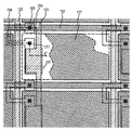
上記のようなアクティブマトリクス基板では、駆動回路に電源や入力信号を供給するために、アクティブマトリクス基板上に、駆動回路と接続した接続配線を作製し、接続配線とFPC(Flexible Print Circuit)を実装する構造が採用されている。基板上の接続配線とFPCの接続には異方性導電膜が用いられている。図30に異方性導電膜によってFPCに接続された接続配線の断面構造を示す。
【0006】
【発明が解決しようとする課題】
図30に示すように、アクティブマトリクス基板において、ガラス基板1の表面の絶縁膜2上に接続配線3が形成されている。FPC4はポリイミドなどでなる可撓性の基板5上に銅などからなる多数の配線6が形成されている。異方性導電膜7には、導電性スペーサ8が、熱や光により硬化する接着剤9(樹脂)内に分散されている。接続配線3とFPC4の上の配線6は導電性スペーサ8によって電気的に接続されている。
【0007】
接続配線3は、アルミニウムやチタンなどの金属膜3aとITO膜等の透明導電膜3bの2多層構造となっている。透明導電膜3bとしてアルミニウムなどの金属膜を用いることで配線抵抗を低くできるが、金属膜3aが導電性スペーサ8に押されて変形するおそれがある。透明導電膜3bはインジウムやスズなどの金属の酸化物でなるため、金属膜3aよりも硬度が高い。そこで、透明導電膜3bを表面に形成することで、金属膜3aの破損や変形を防止している。
【0008】
しかしながら、金属膜3aの側面は異方性導電膜7が形成されるまでは剥き出しの状態で、外気に曝されているため、腐食や酸化されやすい状態となっており、接続配線3とFPC4との接続の信頼性を下げる原因となる。また、FPC4が実装された状態では、金属膜3aの側面は樹脂と接しているため、水分に対する保護に問題がある。
【0009】
本発明は上述した問題点を解消して、FPCと配線の信頼性の高い接続を実現し、かつ量産に適した接続配線を提供することを目的とする。
【0010】
【課題を解決するための手段】
上述の課題を課題を解決するために、本発明は基板上の接続配線を異方性導電膜によって他の基板上の配線と電気的に接続するコンタクト構造であって、
前記引き出し配線は金属膜と透明導電膜の積層膜でなり、前記異方性導電膜との接続部分において、前記金属膜の側面は保護膜に覆われていることを特徴とする。
【0011】
また、他の構成は、基板上に、薄膜トランジスタが配置された回路と、前記薄膜トランジスタでなる回路を他の回路と接続するための接続配線と、を有する半導体装置であって、
前記接続配線金属膜と透明導電膜の積層膜でなり、前記他の回路との接続部分において前記金属膜側面は保護膜に覆われていることを特徴とする。
【0012】
また、他の構成は薄膜トランジスタが配置された回路を有する第1の基板と、前記第1の基板に対向する第2の基板とを有する半導体装置であって、
前記第1の基板上には、前記薄膜トランジスタが配置された回路を他の回路と接続するための、金属膜と、該金属膜表面に接する透明導電膜とでなる接続配線と、前記金属膜の側面に接する保護膜が形成されていることを特徴とする。
【0013】
また、他の構成は薄膜トランジスタが配置された回路を有する第1の基板と、前記第1の基板に対向する第2の基板とを有する半導体装置であって、
前記第1の基板上には、前記薄膜トランジスタが配置された回路を他の回路と接続するための、金属膜と、該金属膜表面に接する透明導電膜とでなる接続配線と、前記薄膜トランジスタ上に形成され、前記第1の基板と前記第2の基板間隔を維持するための柱状スペーサと、前記金属膜の側面に接する前記柱状スペーサと同じ材料でなる保護膜が形成されていることを特徴とする。
【0014】
【発明の実施の形態】
[実施形態1]
本発明のコンタクト構造は、異方性導電膜によって回路を接続する実装方法を用いる半導体装置、例えば、アクティブマトリクス型液晶表示装置や、EL表示装置に好適である。本実施形態では、図12を用いて、本発明をアクティブマトリクス型の液晶表示装置に適用した場合のコンタクト構造を説明する。
【0015】
アクティブマトリクス基板上の接続配線183は端子部182において異方性導電膜195によって、FPC191に電気的に接続される。接続配線183はアクティブマトリクス基板上のTFTのソース/ドレイン配線と同じ工程で作製される。即ち、ソース/ドレイン配線と同じ材料で、同じ層に形成されている。金属膜140と透明導電膜141の積層膜でなる。異方性導電膜195との接続部分において、接続配線183の側面は絶縁材料でなる保護膜173に覆われている。
【0016】
この構造により、接続配線183の金属膜140の側面は保護膜174で覆われる。従って、接続部分において、金属膜140は透明導電膜141、絶縁膜109、保護膜174に接して囲まれ、外気に触れることがない。よって金属膜140の腐食を防止することができる。
【0017】
保護膜174はソース/ドレイン配線の上層に形成される絶縁膜を用いて作製することができる。本実施形態では、保護膜174はアクティブマトリクス基板と対向基板の間隔を保持するために作製された柱状スペーサ172と同じ工程で作製されている。
【0018】
また、図16に示すように接続配線304をTFTのゲート配線配線と同じ工程で作製することもできる。この場合には、接続配線304はゲート配線と同じ材料で同じ層に形成されることになる。また、この場合には、保護膜303はゲート配線とソース/ドレイン配線の間に形成された絶縁膜138、139で作製される。
【0019】
本発明において、接続配線は金属膜の表面を透明導電膜で覆った積層膜で形成される。金属膜は単層膜に限定されない。金属膜の厚さは100nm〜1μmとする。金属膜としては、アルミニウム(Al)、タンタル(Ta)、チタン(Ti)、モリブデン(Mo)、タングステン(W)から選ばれた元素を主成分とする金属膜や、金属元素を含む合金膜を少なくとも1層含むが、これら金属層、合金層の単層膜または多層膜であってももちろんよい。合金としては、Mo−W合金、Mo−Ta合金や、列記した元素と窒素の化合物である窒化タンタル(TaN)、窒化タングステン(WN)、窒化チタン(TiN)膜、窒化モリブデン(MoN)が挙げられる。またタングステンシリサイド、チタンシリサイド、モリブデンシリサイドなどシリサイドを用いることもできる。
【0020】
透明導電膜の厚さは50nm〜0.5μmとする。透明導電膜の材料は、酸化インジウム(In2O3)や酸化インジウム酸化スズ合金(In2O3―SnO2;ITO)などをスパッタ法や真空蒸着法などを用いて形成して用いることができる。このような材料のエッチング処理は塩酸系の溶液により行う。しかし、特にITOのエッチングは残渣が発生しやすいので、エッチング加工性を改善するために酸化インジウム酸化亜鉛合金(In2O3―ZnO)を用いても良い。酸化インジウム酸化亜鉛合金は表面平滑性に優れ、ITOに対して熱安定性にも優れているので、ドレイン配線169の端面で接触するAlとの腐蝕反応を防止できる。同様に、酸化亜鉛(ZnO)も適した材料であり、さらに可視光の透過率や導電率を高めるためにガリウム(Ga)を添加した酸化亜鉛(ZnO:Ga)などを用いることができる。
【0021】
[実施形態2]
また、ゲート配線と同じ工程で接続配線を作製した場合、ゲート配線、接続配線の断面形状をテーパー形状としてもよい。ゲート配線をテーパ状にすることにより、膜厚が中央から側面に向かって減少することとなるので、後述する実施例で示すように、ゲート配線をマスクにした半導体膜のドーピングにおいて、膜厚の変化を利用して半導体膜に添加される不純物濃度を変化させることができる。
【0022】
テーパ形状にするためには、高密度プラズマを用いたドライエッチング法を適用する。高密度プラズマを得る手法にはマイクロ波や誘導結合プラズマ(Inductively Coupled Plasma:ICP)を用いたエッチング装置が適している。特に、ICPエッチング装置はプラズマの制御が容易であり、処理基板の大面積化にも対応できる。
【0023】
ICPを用いたプラズマ処理装置では、プラズマ処理を高精度に行うための手段として、高周波電力をインピーダンス整合器を介して4本の渦巻き状コイル部分が並列に接続されてなるマルチスパイラルコイルに印加してプラズマを形成する方法を用いている。ここで、各コイル部分の1本当たりの長さは、高周波の波長の1/4倍としている。さらに、被処理物を保持する下部電極にも、別途高周波電力を印加してバイアス電圧を付加する構成としている。ICPを用いたプラズマ処理方法やプラズマ処理装置に関しては特開平9−293600号公報等で開示されている。
【0024】
このようなICPを用いたプラズマ処理装置(例えば、エッチング装置)の構造概略図を図25に示す。チャンバー上部の石英板11上にアンテナコイル12を配置し、マッチングボックス13を介してRF電源14に接続されている。また、アンテナコイルに対向して下部電極15が設けられ、下部電極15にプラズマ処理する基板10が配置される。また下部電極15にもマッチングボックス16を介してRF電源17が接続されており、基板上方のアンテナコイル12にRF電流が印加されると、アンテナコイル12にRF電流Jがα方向に流れ、式1に従ってZ方向に磁界Bが発生する。
【0025】
s
μ0 J=rotB(μ0 は透磁率) (式1)
【0026】
そして、ファラデーの電磁誘導の法則に従い、θ方向に誘導電界Eが生じる(式2)。
【0027】
−∂B/∂t=rotE (式2)
【0028】
誘導電界Eで電子がα方向に加速されてガス分子と衝突し、プラズマが生成される。誘導電界の方向がα方向なので、荷電粒子がエッチングチャンバー壁や、基板に衝突して電荷を消失する確率が低くなる。従って、1Pa程度の低圧力でも高密度のプラズマを発生させることができる。また、下流へは、磁界Bがほとんどないので、シート状に広がった高密度プラズマ領域となる。
ICPで高密度プラズマを得る為にはアンテナコイルに流れる高周波電流Jを低損失で流す必要があり、そのインダクタンスを低下させなければならない。そのために、アンテナコイルを分割した方式とすることが有効となる。
【0029】
アンテナコイル12(ICPパワーが印加される)と基板側の下部電極15(バイアスパワーが印加される)のそれぞれに印加するRFパワーを調節することによってプラズマ密度と自己バイアス電圧を独立に制御することが可能である。
また、被エッチング膜に応じて異なる周波数のRFパワーを印加できる。
【0030】
ICPエッチング装置で高密度プラズマを得るためには、アンテナコイル12に流れるRF電流Jを低損失で流す必要があり、大面積化するためには、アンテナコイル12のインダクタンスを低下させなければならない。そのために図26に示したようにアンテナを分割したマルチスパイラルコイル22のICPエッチング装置が開発された。図26中の21は石英板、23、26はマッチングボックス、24、27はRF電源である。また、チャンバーの底部には、基板28を保持する下部電極25が絶縁体29を介して設けられている。
【0031】
このようなマルチスパイラルコイルを適用したICPを用いたエッチング装置を用いると、前記耐熱性導電性材料のエッチングを良好に行うことができまた所望のテーパー角θを有する配線を形成することができる。
【0032】
所望のテーパー角θを得るには、ICPエッチング装置のバイアスパワー密度を調節する。図27は、テーパー角θのバイアスパワー依存性を示した図である。図27に示したように、バイアスパワー密度に応じてテーパー角θを制御することができる。図27は、ガラス基板上に所定のパターンに形成されたW(タングステン)膜について、そのパターン端部のテーパー形状(テーパー角)について調べた結果を示す。図27はテーパー角の基板側にかけるバイアス電力(13.56MHz)依存性を示す。共通条件として放電電力(コイルに印加する高周波電力、13.56MHz)を3.2W/cm2、圧力1.0PaとしてエッチングガスにCF4とCl2を用いた。エッチングガスの流量はCF4、Cl2共に30SCCMとした。
【0033】
図27に示すようにテーパー角はバイアス電力が128〜384mW/cm2の範囲で70〜20°まで変化させることが可能であることが明らかとなった。なお、CF4、Cl2の流量は共に30SCCMとした。
【0034】
また、図28の実験からはテーパー角は60〜80°まで変化させることが可能であ流ことが分かる。なお、図28の実験条件では、テーパー角のエッチングガス流量比依存性について調べた結果を示す。なお、CF4とCl2の合計の流量を60SCCMとして、CF4のみを20〜40SCCMの範囲で変化させた。このときバイアス電力は128mW/cm2とした。
【0035】
更にテーパー角θはタングステンとレジストのエッチングの選択比に依存していると考えられる。図29にタングステンとレジストの選択比とテーパー角θとの依存性を示した。このようにICPエッチング装置を用いて、バイアスパワー密度や反応ガス流量比を適宜決定することで、極めて容易に所望のテーパー角θが3°〜60°の配線を形成することが可能である。
【0036】
また、耐熱性導電性材料のICPエッチング装置における加工特性を考える。
ここでは、W(タングステン)膜とTa(タンタル)膜の他に、ゲート電極用の材料としてしばしば用いられるモリブデンータングステン(Mo−W)合金(組成比はMo:W=48:50wt%)について、エッチング速度、適用するエッチングガス、およびゲート電極の下地となるゲート絶縁膜との選択比の代表的な値を示す。ゲート絶縁膜はプラズマCVD法で作製する酸化シリコン膜または酸化窒化シリコン膜であり、ここで選択比はゲート絶縁膜のエッチング速度に対するそれぞれの材料のエッチング速度の割合として定義する。
【0037】
【表1】

Ta膜はエッチング速度が140〜160nm/minであり、ゲート絶縁膜とのエッチングの選択比が6〜8である。この値はW膜のエッチング速度が70〜90nm/minの範囲でゲート絶縁膜との選択比が2〜4というよりも優れた値となっている。従って、被加工性という観点からはTa膜も適しているが、表中に示さない値として、Ta膜は抵抗率が20〜30μΩcmであり、W膜の10〜16μΩcmに比べて若干高い点が難点となる。
一方、Mo−W合金はエッチング速度が40〜60nm/minと遅く、またゲート絶縁膜に対するエッチングの選択比は0.1〜2となり、この材料は被加工性という観点から必ずしも適していないことが覗われる。このように、表1からはTa膜が最も良い結果を示していることがわかるが、前述のように抵抗率を考慮するとW膜が総合的には適していると考えられる。
【0039】
また、ドライエッチングに用いるエッチングガスとしてフッ素を含むガスと、塩素を含むガスの混合ガスを用いることができる。フッ素を含むガスとしてはCF4、C2F6、またはC4F8から選ばれたガスを用いることができる。また塩素を含むガスとしてはCl2Cl2、SiCl4ガス、BCl4から選ばれたガスを用いることができる。
【0040】
【実施例】
[実施例1]
本実施例は、アクティブマトリクス型液晶パネルに関するものである。図1(A)は本実施例のアクティブマトリクス基板の上面図であり、画素部、画素部の薄膜トランジスタを駆動するための駆動回路部とが形成されている。アクティブマトリクス基板上に作製された柱状スペーサおよびシール剤の位置関係を示す上面図である。
【0041】
図1(A)に示すように、ガラス基板101上には、薄膜トランジスタが配置された画素部188と、画素部188に配置された薄膜トランジスタを駆動するための駆動回路として、走査信号駆動回路185と映像信号制御回路184が設けられている。さらに、その他CPUやメモリなどの信号処理回路187が設けられている。
【0042】
画素部188では走査信号駆動回路185から延在するゲート配線189と映像信号制御回路184から延在するソース配線190がマトリクス状に交差して画素を形成し、各画素にはそれぞれ画素TFT204と保持容量205が設けられている。
【0043】
柱状スペーサ172はアクティブマトリクス基板と、対向基板の間隔を保持するものであって、樹脂でなる円柱状の構造物である。画素部188において設けられる柱状スペーサ172は、すべての画素に対して設けても良いが、マトリクス状に配列した画素の数個から数十個おきに設けても良い。即ち、画素部を構成する画素の全数に対するスペーサの数の割合は20〜100%とすると良い。また、各回路184、185、187には柱状スペーサ172の代わりに、樹脂を回路全面を覆うように設けても良い。本実施例では、TFTのソースおよびドレイン配線の位置にあわせて、円柱状のスペーサを設けている。
【0044】
シール剤186は、基板101上の画素部188および走査信号制御回路185、映像信号制御回路184、その他の信号処理回路187の外側であって、外部入出力端子182よりも内側に形成されている。
【0045】
また、アクティブマトリクス基板100上の回路184、185、187は接続配線183によって、外部の電源や回路に電気的に接続されている。また接続配線183は回路184、185、187のTFTのソース(ドレイン)配線と同時に形成されている。端子部182は接続配線183と一体的に形成され、他の基板上の配線との接続部になる。図1(B)に端子部182の部分拡大図を示す。
【0046】
図1(B)に示すように、端子部182の側面は保護膜174によって覆われており、接続配線183は端子部182において、異方性導電膜によってFPC191の配線191bと電気的に接続されている。191aはFPC191が設けられている基板を指す。
【0047】
図2はアクティブマトリクス基板100の回路のブロック図である。映像信号制御回路184は、シフトレジスタ回路501a、レベルシフタ回路502a、バッファ回路503a、サンプリング回路504を備えている。また、走査信号駆動回路185は、シフトレジスタ回路501b、レベルシフタ回路502b、バッファ回路503bを備えている。
【0048】
シフトレジスタ回路501a、501bは駆動電圧が5〜16V(代表的には10V)であり、この回路を形成するCMOS回路はTFTは、図6に示すの第1のpチャネル型TFT200と第1のnチャネル型TFT201で形成する。
また、レベルシフタ回路502a、502bやバッファ回路503a、503bは駆動電圧が14〜16Vと高くなるがシフトレジスタ回路と同様なTFTを用いれば良い。また、これらの回路において、ゲートをマルチゲート構造で形成すると耐圧が高まり、回路の信頼性を向上させる上で有効である。
【0049】
サンプリング回路504はアナログスイッチから成り、駆動電圧が14〜16Vであるが、極性が交互に反転して駆動される上、オフ電流値を低減させる必要があるため、図6で示す第2のpチャネル型TFT202と第2のnチャネル型TFT203で形成することが望ましい。この回路において、pチャネル型TFT202のオフ電流値が問題となるときは、実施例2で示す工程で作製した、オフセット領域を設けたシングルドレイン構造のTFTで作製すると良い。
【0050】
また、画素部は駆動電圧が14〜16Vであり、低消費電力化の観点からサンプリング回路よりもさらにオフ電流値を低減することが要求され、図6で示す画素TFT204のようにマルチゲート構造とし、さらにLDD領域を設けた構造とするのが望ましい。
【0051】
なお、画素部188と駆動回路185、186のブロック構成のみを示したが、後述するTFTの工程に従えば、その他にも信号分割回路、分周波回路、D/Aコンバータ、γ補正回路、オペアンプ回路、さらにメモリ回路や演算処理回路などの信号処理回路187、さらに論理回路を同一基板上に形成することが可能である。このように、本発明は同一基板上に画素部とその駆動回路とを含む半導体装置、例えば信号制御回路および画素部を具備した液晶表示装置を実現することができる。
【0052】
以下、アクティブマトリクス基板の作製工程を説明する。図3〜図7は画素部188、駆動回路の作製工程を示す断面図であり、図9〜図11は接続配線183の端子部182の作製工程を示す図である。これら図面において同じ符号は同じ構成要素を示している。
【0053】
基板101にはコーニング社の#7059ガラスや#1737ガラスなどに代表されるバリウムホウケイ酸ガラスやアルミノホウケイ酸ガラスなどのガラス基板の他に、ポリエチレンテレフタレート(PET)、ポリエチレンナフタレート(PEN)、ポリエーテルサルフォン(PES)など光学的異方性を有しないプラスチック基板を用いることができる。ガラス基板を用いる場合には、ガラス歪み点よりも10〜20℃程度低い温度であらかじめ熱処理しておいても良い。そして、基板101のTFTを形成する表面に、基板101からの不純物拡散を防ぐために、酸化シリコン膜、窒化シリコン膜または酸化窒化シリコン膜などの下地膜102を形成する。例えば、プラズマCVD法でSiH4、NH3、N2Oから作製される酸化窒化シリコン膜102aを10〜200nm(好ましくは50〜100nm)、同様にSiH4、N2Oから作製される酸化窒化水素化シリコン膜102bを50〜200nm(好ましくは100〜150nm)の厚さに積層形成する(図3(A))。
【0054】
酸化窒化シリコン膜は従来の平行平板型のプラズマCVD法を用いて形成する。酸化窒化シリコン膜102aは、SiH4を10SCCM、NH3を100SCCM、N2Oを20SCCMとして反応室に導入し、基板温度325℃、反応圧力40Pa、放電電力密度0.41W/cm2、放電周波数60MHzとした。一方、酸化窒化水素化シリコン膜102bは、SiH4を5SCCM、N2Oを120SCCM、H2を125SCCMとして反応室に導入し、基板温度400℃、反応圧力20Pa、放電電力密度0.41W/cm2、放電周波数60MHzとした。これらの膜は、基板温度を変化させ、反応ガスの切替えのみで連続して形成することもできる。
【0055】
このようにして作製した酸化窒化シリコン膜102aは、密度が9.28×10²²/cm3であり、フッ化水素アンモニウム(NH4HF2)を7.13%とフッ化アンモニウム(NH4F)を15.4%含む混合溶液(ステラケミファ社製、商品名LAL500)の20℃におけるエッチング速度が約63nm/minと遅く、緻密で硬い膜である。このような膜を下地膜に用いると、この上に形成する半導体膜にガラス基板からのアルカリ金属元素が拡散するのを防ぐのに有効である。
【0056】
次に、25〜80nm(好ましくは30〜60nm)の厚さで非晶質構造を有する半導体膜103aを、プラズマCVD法やスパッタ法などの公知の方法で形成する。例えば、プラズマCVD法で非晶質シリコン膜を55nmの厚さに形成する。非晶質構造を有する半導体膜には、非晶質半導体膜や微結晶半導体膜があり、非晶質シリコンゲルマニウム膜などの非晶質構造を有する化合物半導体膜を適用しても良い。また、下地膜102と非晶質半導体膜103aとは両者を連続形成することも可能である。例えば、前述のように酸化窒化シリコン膜102aと酸化窒化水素化シリコン膜102bをプラズマCVD法で連続して成膜後、反応ガスをSiH4、N2O、H2からSiH4とH2或いはSiH4のみに切り替えれば、一旦大気雰囲気に晒すことなく連続形成できる。その結果、酸化窒化水素化シリコン膜102bの表面の汚染を防ぐことが可能となり、作製するTFTの特性バラツキやしきい値電圧の変動を低減させることができる。
【0057】
そして、結晶化の工程を行い非晶質半導体膜103aから結晶質半導体膜103bを作製する。その方法としてレーザーアニール法や熱アニール法(固相成長法)、またはラピットサーマルアニール法(RTA法)を適用することができる。前述のようなガラス基板や耐熱性の劣るプラスチック基板を用いる場合には、特にレーザーアニール法を適用することが好ましい。RTA法では、赤外線ランプ、ハロゲンランプ、メタルハライドランプ、キセノンランプなどを光源に用いる。或いは特開平7−130652号公報で開示された技術に従って、触媒元素を用いる結晶化法で結晶質半導体膜103bを形成することもできる。結晶化の工程ではまず、非晶質半導体膜が含有する水素を放出させておくことが好ましく、400〜500℃で1時間程度の熱処理を行い含有する水素量を5atom%以下にしてから結晶化させると膜表面の荒れを防ぐことができるので良い。
【0058】
結晶化をレーザーアニール法にて行う場合には、パルス発振型または連続発光型のエキシマレーザーやアルゴンレーザーをその光源とする。パルス発振型のエキシマレーザーを用いる場合には、レーザー光を線状に加工してレーザーアニールを行う。レーザーアニール条件は実施者が適宣選択するものであるが、例えば、レーザーパルス発振周波数30Hzとし、レーザーエネルギー密度を100〜500mJ/cm2(代表的には300〜400mJ/cm2)とする。そして線状ビームを基板全面に渡って照射し、この時の線状ビームの重ね合わせ率(オーバーラップ率)を80〜98%として行う。このようにして図3(B)に示すように結晶質半導体膜103bを得ることができる。
【0059】
そして、結晶質半導体膜103b上にフォトリソグラフィーの技術によって、フォトマスクPM1を用いてレジストパターンを形成し、ドライエッチングによって結晶質半導体膜を島状に分割し、島状半導体膜104〜108を形成しする。ドライエッチングにはCF4とO2の混合ガスを用いる。
【0060】
島状半導体膜に対し、TFTのしきい値電圧(Vth)を制御する目的でp型を付与する不純物元素を1×10¹⁶〜5×10¹⁷atoms/cm3程度の濃度で島状半導体膜の全面に添加しても良い。半導体に対してp型を付与する不純物元素には、ホウ素(B)、アルミニウム(Al)、ガリウム(Ga)など周期律表第13族の元素が知られている。その方法として、イオン注入法やイオンドープ法を用いることができるが、大面積基板を処理するにはイオンドープ法が適している。イオンドープ法ではジボラン(B2H6)をソースガスとして用いホウ素(B)を添加する。このような不純物元素の注入は必ずしも必要でなく省略しても差し支えないが、特にnチャネル型TFTのしきい値電圧を所定の範囲内に収めるために好適に用いる手法である。
【0061】
ゲート絶縁膜109はプラズマCVD法またはスパッタ法を用い、膜厚を40〜150nmとしてシリコンを含む絶縁膜で形成する。例えば、120nmの厚さで酸化窒化シリコン膜から形成すると良い。また、SiH4とN2OにO2を添加させて作製された酸化窒化シリコン膜は、膜中の固定電荷密度が低減されているのでこの用途に対して好ましい材料となる。勿論、ゲート絶縁膜はこのような酸化窒化シリコン膜に限定されるものでなく、他のシリコンを含む絶縁膜を単層または積層構造として用いても良い(図3(C))。
【0062】
図3(D)に示すように、ゲート絶縁膜109上にゲート配線を形成するための導電膜を形成する。導電膜は単層で形成しても良いが、必要に応じて二層あるいは三層といった複数の層から成る積層構造としても良い。例えば、2層の場合には、上層に、タンタル(Ta)、チタン(Ti)、モリブデン(Mo)、タングステン(W)等の元素を主成分とする金属膜やこれら元素の合金膜(代表的にはMo−W合金膜、Mo−Ta合金膜)で形成し、下層は窒化タンタル(TaN)、窒化タングステン(WN)、窒化チタン(TiN)膜、窒化モリブデン(MoN)などで形成する。例えば、2層の場合、上層に下層の導電膜の窒化物で形成すればよく、下層/上層としてWN膜/W膜や、TaN膜/Ta膜膜等とすればよい。また、3層の場合は、TaN膜/Ta膜/TaN膜とすればよい。2層目の(上層の)導電膜は抵抗率を10〜50μΩcmの範囲ですることが好ましい。低抵抗化を図るために含有する不純物濃度を低減させることが好ましく、特に酸素濃度に関しては30ppm以下とすると良かった。例えば、タングステン(W)は酸素濃度を30ppm以下とすることで20μΩcm以下の比抵抗値を実現することができた。
【0063】
また、配線抵抗の低抵抗化には、アルミニウムを主成分とする膜を用いるのが好ましい。この場合、アルミニウムにSiやSc等を微量添加して耐熱性を高めるとよい。例えば、ゲート配線を構成する導電膜として、Ti膜/Scを添加したAl膜や、Ti膜/TiN膜/Scを添加したAl膜を形成すればよい。
【0064】
W膜を成膜する場合には、Wをターゲットとしたスパッタ法で、アルゴン(Ar)ガスと窒素(N2)ガスを導入して導電膜111を窒化タングステン(WN)で50nmの厚さに形成し、導電膜110をWで250nmの厚さに形成する。その他の方法として、W膜は6フッ化タングステン(WF6)を用いて熱CVD法で形成することもできる。いずれにしてもゲート電極として使用するためには低抵抗化を図る必要があり、W膜の抵抗率は20μΩcm以下にすることが望ましい。W膜は結晶粒を大きくすることで低抵抗率化を図ることができるが、W膜中に酸素などの不純物元素が多い場合には結晶化が阻害され高抵抗化する。このことより、スパッタ法による場合、純度99.9999%のWターゲットを用い、さらに成膜時に気相中からの不純物の混入がないように十分配慮してW膜を形成することにより、抵抗率9〜20μΩcmを実現することができる。
【0065】
TaN膜、Ta膜は同様にスパッタ法で形成することが可能である。TaN膜はTaをターゲットとしてスパッタガスにArと窒素との混合ガスを用いて形成し、Ta膜はスパッタガスにArを用いる。また、これらのスパッタガス中に適量のXeやKrを加えておくと、形成する膜の内部応力を緩和して膜の剥離を防止することができる。α相のTa膜の抵抗率は20μΩcm程度でありゲート電極に使用することができるが、β相のTa膜の抵抗率は180μΩcm程度でありゲート電極とするには不向きであった。TaN膜はα相に近い結晶構造を持つので、この上にTa膜を形成すればα相のTa膜が容易に得られた。本実施例では、ゲート配線を構成する導電膜として、下層の導電膜110としてTaN膜を上層の導電膜111としてTa膜を成膜する。
【0066】
またゲート配線を構成する導電膜とゲート絶縁膜109の間に2〜20nm程度の厚さでリン(P)をドープしたシリコン膜を形成しておくことは有効である。これにより、その上に形成される導電膜の密着性向上と酸化防止を図ると同時に、導電膜が微量に含有するアルカリ金属元素がゲート絶縁膜109に拡散するのを防ぐことができる。
【0067】
次に、フォトリソグラフィーの技術によって、フォトマスクPM2を用いてレジストマスクRM1 〜RM6 を形成し、導電膜110と導電膜111とを一括でエッチングしてゲート配線118〜122と容量配線123を形成する。ゲート配線118〜122と容量配線123は導電膜から成る118a〜122aと、導電膜から成る118b〜122bとが一体として形成されている(図4(A))。
【0068】
そして、nチャネル型TFTにLDD領域を形成するために、n型を付与する不純物元素添加の工程(n-ドープ工程)を行った。ここではゲート配線118〜122をマスクとして自己整合的にn型を付与する不純物元素をイオンドープ法で添加した。n型を付与する不純物元素として添加するリン(P)を1×10¹⁶〜5×10¹⁹atoms/cm3の濃度範囲で添加する。このようにして、図4(B)に示すように島状半導体膜に低濃度n型不純物領域124〜129を形成する。
【0069】
次に、nチャネル型TFTにおいて、ソース領域またはドレイン領域として機能する高濃度n型不純物領域の形成を行った(n+ドープ工程)。まず、フォトマスクPM3を用い、レジストのマスクRM8 〜RM12を形成し、n型を付与する不純物元素を添加して高濃度n型不純物領域130〜135を形成した。n型を付与する不純物元素にはリン(P)を用い、その濃度が1×10²⁰〜1×10²¹atoms/cm3の濃度範囲となるようにフォスフィン(PH3)を用いたイオンドープ法で行った(図4(C))。
【0070】
そして、pチャネル型TFTを形成する島状半導体膜104、106にソース領域およびドレイン領域とする高濃度p型不純物領域136、137を形成する。ここでは、ゲート配線118、120をマスクとしてp型を付与する不純物元素を添加し、自己整合的に高濃度p型不純物領域を形成する。
【0071】
この工程では、nチャネル型TFTを形成する島状半導体膜105、107、108は、フォトマスクPM4を用いてレジストマスクRM13〜RM15を形成し全面を被覆しておく。高濃度p型不純物領域136、137はジボラン(B2H6)を用いたイオンドープ法で形成する。この領域のボロン(B)濃度は3×10²⁰〜3×10²¹atoms/cm3となるようにする(図4(D))。
【0072】
高濃度p型不純物領域136、137には、前工程においてリン(P)が添加されていて、高濃度p型不純物領域136a、137aには1×10²⁰〜1×10²¹atoms/cm3の濃度で、高濃度p型不純物領域136b、137bには1×1016〜5×1019atoms/cm3の濃度で含有しているが、この工程で添加するボロン(B)の濃度を1.5から3倍となるようにすることにより、pチャネル型TFTのソース領域およびドレイン領域として機能する上で何ら問題はなかった。
【0073】
その後、図5(A)に示すように、ゲート配線およびゲート絶縁膜109上から保護絶縁膜138を形成する。保護絶縁膜138は酸化シリコン膜、酸化窒化シリコン膜、窒化シリコン膜、またはこれらを組み合わせた積層膜で形成すれば良い。いずれにしても保護絶縁膜138は無機絶縁物材料から形成する。保護絶縁膜138の膜厚は100〜200nmとする。ここで、酸化シリコン膜を用いる場合には、プラズマCVD法で、オルトケイ酸テトラエチル(Tetraethyl Orthosilicate:TEOS)とO2 とを混合し、反応圧力40Pa、基板温度300〜400℃とし、高周波(13.56MHz)電力密度0.5〜0.8W/cm2で放電させて形成することができる。
【0074】
酸化窒化シリコン膜を用いる場合には、プラズマCVD法でSiH4、N2 O、NH3 から作製される酸化窒化シリコン膜、またはSiH4、N2 Oから作製される酸化窒化シリコン膜で形成すれば良い。この場合の作製条件は反応圧力20〜200Pa、基板温度300〜400℃とし、高周波(60MHz)電力密度0.1〜1.0W/cm2で形成することができる。また、SiH4 、N2 O、H2から作製される酸化窒化水素化シリコン膜を適用しても良い。窒化シリコン膜も同様にプラズマCVD法でSiH4、NH3から作製することが可能である。
【0075】
その後、それぞれの濃度で添加されたn型またはp型を付与する不純物元素を活性化する工程を行う。この工程はファーネスアニール炉を用いる熱アニール法で行う。その他に、レーザーアニール法、またはラピッドサーマルアニール法(RTA法)を適用することができる。熱アニール法では酸素濃度が1ppm以下、好ましくは0.1ppm以下の窒素雰囲気中で400〜700℃、代表的には500〜600℃で行うものであり、本実施例では550℃で4時間の熱処理を行った。また、基板101に耐熱温度が低いプラスチック基板を用いる場合にはレーザーアニール法を適用することが好ましい(図5(B))。
【0076】
活性化の工程の後、さらに、3〜100%の水素を含む雰囲気中で、300〜450℃で1〜12時間の熱処理を行い、島状半導体膜を水素化する工程を行った。この工程は熱的に励起された水素により島状半導体膜にある1016〜1018/cm3のダングリングボンドを終端する工程である。水素化の他の手段として、プラズマ水素化(プラズマにより励起された水素を用いる)を行っても良い。
【0077】
活性化および水素化の工程が終了したら、有機絶縁物材料からなる層間絶縁膜139を1.0〜2.0μmの平均厚を有して形成する。有機樹脂材料としては、ポリイミド、アクリル、ポリアミド、ポリイミドアミド、BCB(ベンゾシクロブテン)等を使用することができる。例えば、基板に塗布後、熱重合するタイプのポリイミドを用いる場合には、クリーンオーブンで300℃で焼成して形成する。また、アクリルを用いる場合には、2液性のものを用い、主材と硬化剤を混合した後、スピナーを用いて基板全面に塗布した後、ホットプレートで80℃で60秒の予備加熱を行い、さらにクリーンオーブンで250℃で60分焼成して形成することができる。(図5(C))
【0078】
このように、層間絶縁膜139を有機絶縁物材料で形成することにより、表面を良好に平坦化させることができる。また、有機樹脂材料は一般に誘電率が低いので、寄生容量を低減するできる。しかし、吸湿性があり保護膜としては適さないので、本実施例のように、保護絶縁膜138として形成した酸化シリコン膜、酸化窒化シリコン膜、窒化シリコン膜などと組み合わせて用いる必要がある。
【0079】
その後、フォトマスクPM5を用い、所定のパターンのレジストマスクを形成し、それぞれの島状半導体膜に形成されたソース領域またはドレイン領域に達するコンタクトホールを絶縁膜138、139に形成する。更に、端子部182の絶縁膜138、139を除去する。コンタクトホールの形成はドライエッチング法により行う。この場合、エッチングガスにCF4、O2、Heの混合ガスを用い有機樹脂材料から成る層間絶縁膜139をまずエッチングし、その後、続いてエッチングガスをCF4、O2として保護絶縁膜138をエッチングする。さらに、島状半導体膜との選択比を高めるために、エッチングガスをCHF3に切り替えてゲート絶縁膜をエッチングすることにより、良好にコンタクトホールを形成することができる。
【0080】
そして、ソース/ドレイン配線及び接続配線183を形成する金属膜140と透明導電膜141の積層膜を形成する。ここでは、金属膜140としてTi膜を50〜150nmの厚さで形成し、島状半導体膜のソースまたはドレイン領域を形成する半導体膜とコンタクトを形成し、そのTi膜上に重ねてアルミニウム(Al)を300〜400nmの厚さでスパッタ法で形成する。また、金属膜140として、Ti膜/TiN膜/Al膜でなる積層膜を成膜してもよい。
【0081】
透明導電膜の材料は、酸化インジウム(In2O3)や酸化インジウム酸化スズ合金(In2O3―SnO2;ITO)などをスパッタ法や真空蒸着法などを用いて形成して用いることができる。このような材料のエッチング処理は塩酸系の溶液により行う。しかし、特にITOのエッチングは残渣が発生しやすいので、エッチング加工性を改善するために酸化インジウム酸化亜鉛合金(In2O3―ZnO)を用いても良い。酸化インジウム酸化亜鉛合金は表面平滑性に優れ、ITOに対して熱安定性にも優れているので、ドレイン配線169の端面で接触するAlとの腐蝕反応を防止できる。同様に、酸化亜鉛(ZnO)も適した材料であり、さらに可視光の透過率や導電率を高めるためにガリウム(Ga)を添加した酸化亜鉛(ZnO:Ga)などを用いることができる。本実施例では透明導電膜141として酸化インジウム酸化亜鉛合金を形成する。(図6(A))
【0082】
図9に図6(A)に対応する接続配線183の端子部182部分の構造を示す。(A)は配線の長尺方向に垂直な断面に対応し、(B)は長尺方向に沿った断面図に対応し、TFTとの構造と積層関係が明らかになるようにした。(C)は上面図である。図10、図11も同様である。
【0083】
フォトマスクPM6によりレジストマスクパターンを形成し、エッチングによってソース配線148〜152とドレイン配線153〜158を形成する。及び、図10に示すように接続配線183を形成する。ここで、ドレイン配線157は画素電極として機能するものである。(図6(B)、図10)。
【0084】
この状態で水素化処理を行うとTFTの特性向上に対して好ましい結果が得られた。例えば、3〜100%の水素を含む雰囲気中で、300〜450℃で1〜12時間の熱処理を行うと良く、あるいはプラズマ水素化法を用いても同様の効果が得られた。また、このような熱処理により保護絶縁膜138や、下地膜102にに存在する水素を島状半導体膜104〜108に拡散させ水素化をすることもできる。いずれにしても、島状半導体膜104〜108中の欠陥密度を1016/cm3以下とすることが望ましく、そのために水素を0.01〜0.1atomic%程度付与すれば良かった。
【0085】
こうして6枚のフォトマスクにより、同一の基板上に、駆動回路のTFTと画素部の画素TFTとを有した基板を完成させることができる。駆動回路には第1のpチャネル型TFT200、第1のnチャネル型TFT201、第2のpチャネル型TFT202、第2のnチャネル型TFT203、画素部には画素TFT204、保持容量205が形成されている。本明細書では便宜上このような基板をアクティブマトリクス基板と呼ぶ。
【0086】
駆動回路の第1のpチャネル型TFT200には、島状半導体膜104にチャネル形成領域206、高濃度p型不純物領域から成るソース領域207a、207b、ドレイン領域208a,208bを有したシングルドレインの構造を有している。
【0087】
第1のnチャネル型TFT201の島状半導体膜105には、チャネル形成領域209、ゲート電極119と重ならないLDD領域210、ソース領域212、ドレイン領域211が形成されている。LDD領域210のチャネル長方向の長さは1.0〜4.0μm、好ましくは2.0〜3.0μmとした。nチャネル型TFTにおけるLDD領域の長さをこのようにすることにより、ドレイン領域近傍に発生する高電界を緩和して、ホットキャリアの発生を防ぎ、TFTの劣化を防止することができる。
【0088】
サンプリング回路の第2のpチャネル型TFT202の島状半導体膜106には、チャネル形成領域213、高濃度p型不純物領域から成るソース領域214a、214b、ドレイン領域215a、215bが形成され、シングルドレインの構造となっている。
【0089】
第2のnチャネル型TFT203には、島状半導体膜107にチャネル形成領域216、LDD領域217、218、ソース領域220、ドレイン領域219が形成されている。LDD領域217、218の長さは1.0〜4.0μmとする。
【0090】
画素TFT204には、島状半導体膜108にチャネル形成領域221、222、LDD領域223〜225、ソースまたはドレイン領域226〜228を有している。LDD領域のチャネル長方向の長さは0.5〜4.0μm、好ましくは1.5〜2.5μmである。更に画素TFT204には保持容量が接続されている。保持容量205は、ゲート絶縁膜209を誘電体にし、容量配線123と画素TFT204のドレイン領域228に接続する半導体膜229を電極にするコンデンサーである。図6(B)では画素TFT204をダブルゲート構造としたが、シングルゲート構造でも良いし、複数のゲート電極を設けたマルチゲート構造としても差し支えない。
【0091】
図13は画素部のほぼ一画素分を示す上面図である。図中に示すA−A'断面が図6(B)に示す画素部の断面図に対応している。画素TFT204は、ゲート配線を兼ねるゲート電極122は、図示されていないゲート絶縁膜を介してその下の島状半導体膜108と交差している。図示はしていないが、島状半導体膜108には、ソース領域、ドレイン領域、LDD領域が形成されている。また、256はソース配線152とソース領域226とのコンタクト部、257はドレイン配線157とドレイン領域228とのコンタクト部である。保持容量205は、画素TFT204のドレイン領域228から延在する半導体膜229とゲート絶縁膜を介して容量配線123が重なる領域で形成されている。この構成において半導体膜229には、価電子制御を目的とした不純物元素は添加されていない。
【0092】
以上の様な構成は、画素TFTおよび駆動回路が要求する仕様に応じて各回路を構成するTFTの構造を最適化し、半導体装置の動作性能と信頼性を向上させることを可能としている。さらにゲート電極を耐熱性を有する導電性材料で形成することによりLDD領域やソース領域およびドレイン領域の活性化を容易としている。
【0093】
更に本実施例では、図7に示すように、上述した工程を経たアクティブマトリクス基板からに柱状スペーサ172を形成する。同時に、柱状スペーサ172を作製すると共に、接続配線183の端子部182の側面を保護する保護膜174を形成する。柱状スペーサ172の材料に限定はないが、例えば、JSR社製のNN700を用い、スピナーで塗布した後、露光と現像処理によって所定のパターンに形成する。さらにクリーンオーブンなどで150〜200℃で加熱して硬化させる。
【0094】
このようにして作製されるスペーサは露光と現像処理の条件によって形状を異ならせることができるが、好ましくは、図14で示すように、柱状スペーサ172の形状は柱状で頂部が平坦な形状となるようにすると、対向側の基板を合わせたときに液晶表示パネルとしての機械的な強度を確保することができる。形状は円錐状、角錐状など特別の限定はないが、例えば円錐状としたときに具体的には、高さHを1.2〜5μmとし、平均半径L1を5〜7μm、平均半径L1と底部の半径L2との比を1対1.5とする。このとき側面のテーパー角は±15°以下とする。
【0095】
スペーサの配置は任意に決定すれば良いが、好ましくは、図7に示すように、画素部188においてはドレイン配線157(画素電極)のコンタクト部251と重ねてその部分を覆うように柱状スペーサ172を形成すると良い。コンタクト部251は平坦性が損なわれこの部分では液晶がうまく配向しなくなるので、このようにしてコンタクト部251にスペーサ用の樹脂を充填する形で柱状スペーサ172を形成することで、ディスクリネーションなどを防止することができる。
【0096】
図11に示すように、柱状スペーサ172の作製過程で、接続配線183の側面を保護する保護膜174が形成される。保護膜174は端子部182において、透明導電膜141の表面だけを露出するように形成される。保護膜174の形状は露光と現像処理の条件によって決定できる。この構成により、接続配線183の端子部182において、金属膜140は保護膜174、ゲート絶縁膜109、及び透明導電膜141接して、覆われるため、外気に曝されることがない。
【0097】
その後、基板101の表面に配向膜173を形成する。端子部182には配向膜173は形成されない。通常液晶表示素子の配向膜にはポリイミド樹脂が用いられる。配向膜173を形成した後、ラビング処理を施して液晶分子がある一定のプレチルト角を持って配向するようにした。画素部に設けた柱状スペーサ172の端部からラビング方向に対してラビングされない領域が2μm以下となるようにした。また、ラビング処理では静電気の発生がしばしば問題となるが、駆動回路のTFT上にもスペーサ172を形成しておくと、スペーサとしての本来の役割と、静電気からTFTを保護する効果を得ることができる。
【0098】
以上により、基板間隔を保持する柱状スペーサ172が基板101と一体化したアクティブマトリクス基板が完成する。なお、配向膜173を形成した後、柱状スペーサ172を形成した構成とすることもできる。(図7、図11)
【0099】
アクティブマトリクス基板と対になる対向基板には、図8に示すように、基板251上に遮光膜252、図示しないカラーフィルター、透明導電膜253および配向膜254が形成されている。遮光膜252はTi、Cr、Alなどを150〜300nmの厚さで形成する。
【0100】
そして、図8に示すように画素部と駆動回路が形成されたアクティブマトリクス基板と対向基板とをシール剤179で貼り合わせる。シール剤179にはフィラーが混入されていて、このフィラーと柱状スペーサ172によって均一な間隔を持って2枚の基板が貼り合わせられる。そして、基板の隙間に液晶材料260を注入し、封止剤(図示せず)によって完全に封止して、液晶パネルが完成する。
【0101】
更に、アクティブマトリクス基板100上の回路を映像信号を入力するための回路や、電力を供給するための電源等に接続するため、図12に示すように、端子部182において、接続配線183とFPC191を異方性導電膜195によって電気的に接続する。図12(A)は端子部182の配線の長尺方向と垂直な面の断面図であり、図12(B)は長尺方向に沿った断面である。
【0102】
図12に示すように異方性導電膜195は接着剤195a内に金やクロムなどでメッキされた数十〜数百μm粒子195bにより構成され、この粒子195bが接続配線183とFPCの配線191bとに接触することにより、アクティブマトリクス基板100とFPC191電気的に接続することができる。FPC191は基板101との接着強度を高めるために、外端子部182の外側にはみだしており、端部には樹脂層192が設けられ、機械的強度を高めている。
【0103】
[実施例2]
実施例1では、接続配線183をTFTのソース/ドレイン配線と同じ作製工程で作製したが、本実施例では、ゲート配線と同じ工程で接続配線183を作製するとする。図15を用いて、本実施例を説明する。TFTの作製工程は実施例1を用いる。図15において、図3〜図8と同じ符号は同じ構成要素をさす。
【0104】
まず、実施例1の作製工程に従って、図9(C)の工程までを行う。次に、ゲート配線を構成する導電膜301と透明導電膜302の積層膜を成膜する。導電膜301は実施例1述べたゲート配線を構成する導電膜110や111の材料を用いればよい。また透明導電膜302としては、TFTのソース/ドレイン配線の表面に形成された透明導電膜141と同じ材料を用いることができる。ここでは、導電膜301として、WN膜/W膜の積層膜をスパッタ法で成膜し、透明導電膜としてITO膜を成膜する(図15(A))。
【0105】
そして、図4(A)に示すようにレジストマスクを形成し、導電膜301と透明導電膜302をエッチングして、TFTのゲート配線及び図15(B)に示すように接続配線304を形成する。Wを主成分とする材料で形成されている場合には、高速でかつ精度良くエッチングを実施するために高密度プラズマを用いたドライエッチング法を適用することが望ましい。
【0106】
高密度プラズマを得る手法の一つとして、誘導結合プラズマ(Inductively Coupled Plasma:ICP)エッチング装置を用いると良い。ICPエッチング装置を用いたWのエッチング法は、エッチングガスにCF4とCl2の2種のガスを反応室に導入し、圧力0.5〜1.5Pa(好ましくは1Pa)とし、誘導結合部に200〜1000Wの高周波(13.56MHz)電力を印加する。この時、基板が置かれたステージには20Wの高周波電力が印加され、自己バイアスで負電位に帯電することにより、正イオンが加速されて異方性のエッチングを行うことができる。ICPエッチング装置を使用することにより、Wなどの硬い金属膜も2〜5nm/秒のエッチング速度を得ることができる。また、残渣を残すことなくエッチングするためには、10〜20%程度の割合でエッチング時間を増しオーバーエッチングをすると良い。
【0107】
しかし、この時に下地とのエッチングの選択比に注意する必要がある。例えば、W膜に対する酸化窒化シリコン膜(ゲート絶縁膜109)の選択比は2.5〜3であるので、このようなオーバーエッチング処理により、酸化窒化シリコン膜が露出した面は20〜50nm程度エッチングされて実質的に薄くなる。
【0108】
そして、実施例1で説明したようにTFTの半導体膜にリン、ボロンを添加し、図5(A)に示すように保護絶縁膜138を形成し、半導体膜に添加したリン、ボロンを活性化する(図15(C))。
【0109】
そして、図5(C)に示すように層間絶縁膜139を形成する。層間絶縁膜139の材料は実施例1で説明したた材料を選択すればよく、シリコン系の無機絶縁膜でもよいし、アクリル等の有機樹脂膜でもよい(図15(D))。
【0110】
次に、図6に示すように、保護絶縁膜138に層間絶縁膜139に島状半導体膜に形成されたソース領域またはドレイン領域に達するコンタクトホールを形成すると同時に、接続配線304の端子部において、端子部の側面を覆う保護膜304を形成する(図15(E))。
【0111】
以降の工程は実施例1と同様に実施して、アクティブマトリクス基板100を完成する。そして、アクティブマトリクス基板100と対向基板250をシール剤179によって貼り合わせ液晶材料260を封入し、接続配線304とFPC191を異方性導電膜195によって電気的に接続する(図15(F))。
【0112】
本実施例では、保護膜304によって、接続配線304の導電膜301の側面を覆っているため、導電膜301は保護膜304、ゲート絶縁膜109、透明導電膜302でくるまれた構造となり、外気に曝されることがない。
【0113】
[実施例3] 本実施例は実施例1の変形例であり、ゲート配線の断面形状がテーパ状になるようにしたものであり、また、接続配線をゲート配線と同じ作製工程で作製するようにした例である。図17〜図19を用いて本実施例のアクティブマトリクス基板の作製工程を説明する。ここでは、画素部の画素TFTおよび保持容量と、画素部の周辺に設けられる駆動回路のTFTを同時に作製する方法について工程に従って詳細に説明する。図21に接続配線の作製工程を示す。
【0114】
図17(A)において、ガラス基板601表面に、酸化シリコン膜、窒化シリコン膜または酸化窒化シリコン膜などの絶縁膜から成る下地膜602を形成する。本実施例では、プラズマCVD法でSiH4、NH3、N2Oから成膜される酸化窒化シリコン膜を10〜200nmし、酸化窒化シリコン膜表面にSiH4、N2Oから成膜される酸化窒化水素化シリコン膜602を50〜200nm(好ましくは100〜150nm)の厚さに積層形成する。
【0115】
次に、プラズマCVD法で非晶質シリコン膜を55nmの厚さに形成し、実施例1と同様に結晶化して、結晶質シリコン膜を形成する。そしてフォトマスクPM11を用いて、フォトリソグラフィーの技術により、結晶質シリコン膜上にレジストパターンを形成し、ドライエッチングによって結晶質半導体膜を島状に分割し、島状半導体膜604〜608を形成する。結晶質シリコン膜のドライエッチングにはCF4とO2の混合ガスを用いる。次に、ゲート絶縁膜609はプラズマCVD法で120nmの厚さで酸化窒化シリコン膜から形成する。
【0116】
そして、ゲート絶縁膜609上にゲート配線を形成するために金属膜611、612と透明導電膜613の積層膜を耐熱性導電膜を形成する。金属膜611をWN膜で、金属膜膜612をW膜で形成し、透明導電膜613に酸化インジウム酸化亜鉛合金(In2O3―ZnO)を成膜する(図17(A)、図21(A))。
【0117】
第2のフォトマスクPM12を用い、フォトリソグラフィーの技術を使用してレジストマスクRM21〜RM27を形成し、透明導電膜613をエッチングして、ゲート配線618〜622と容量配線623、接続配線683の最上層618a〜623a、683aを形成する。(図17(B)、図21(B))
【0118】
透明導電膜でなる最上層618a〜623a、683aの側面は図18(B)、図21(B)に示すように、レジストマスクRM21〜RM27よりも後退するようにエッチングされる。次に、
金属膜611、613を一括でエッチングして、テーパー状の断面を有するゲート配線618〜6、22、容量配線623及び接続配線683が完成する。(図17(C)、図21(C))
【0119】
配線618〜623、683は、透明導電膜613でなる層618a〜623a、683aと、金属膜612でなる層618b〜623b、683bと、金属膜611でなる層618c〜623c、683cが積層された構造となる。
【0120】
このとき少なくともゲート配線618〜622の端部にテーパー部が形成されるようにエッチングする。このエッチング加工はICPエッチング装置により行う。エッチングガスにCF4とCl2の混合ガスを用いその流量をそれぞれ30SCCMとして、放電電力3.2mW/cm2(13.56MHz)、バイアス電力224mW/cm2(13.56MHz)、圧力1.0Paでエッチングを行った。このようなエッチング条件によって、ゲート配線618〜622の端部において、該端部から内側にむかって徐々に厚さが増加するテーパー部が形成され、その角度は25〜35°、好ましくは30°となる。テーパー部の角度は、後にLDD領域を形成する低濃度n型不純物領域の濃度勾配に大きく影響する。尚、テーパー部の角度θ1は、テーパー部の長さ(WG)とテーパー部の厚さ(HG)を用いてTan(θ1)=HG/WGで表される。
【0121】
また、残渣を残すことなくエッチングするためには、絶縁膜609の厚さの10〜20%程度の割合でオーバーエッチングする。しかし、この時に下地とのエッチングの選択比に注意する必要がある。例えば、W膜に対する酸化窒化シリコン膜(ゲート絶縁膜609)の選択比は表1で示したように2〜4(代表的には3)であるので、このようなオーバーエッチング処理により、酸化窒化シリコン膜が露出した面は20〜50nm程度エッチングされて実質的に薄くなり、新たな形状のゲート絶縁膜610が形成された。
【0122】
そして、画素TFTおよび駆動回路のnチャネル型TFTのLDD領域を形成するために、n型を付与する不純物元素添加の工程(n-ドープ工程)を行う。ゲート電極の形成に用いたレジストマスク112〜117をそのまま残し、端部にテーパー部を有するゲート配線618〜622をマスクとして自己整合的にn型を付与する不純物元素としてリンをイオンドープ法で添加する(図18(A))。
【0123】
ここでは、n型を付与する不純物元素を配線618〜623のテーパー部とゲート絶縁膜610とを通して、その下に位置する半導体膜に達するように添加するために、加速電圧を高く80〜160keVとし、LDD領域を形成するためにドーズ量を低く、1×10¹³〜5×10¹⁴atoms/cm2とする。半導体膜に添加される不純物の濃度は1×1016〜1×1019atoms/cm3の濃度範囲で添加する。このようにして、図18(A)に示すように島状半導体膜に低濃度n型不純物領域624〜629を形成する。
【0124】
この工程において、低濃度n型不純物領域624〜628において、少なくともゲート配線618〜622に重なった部分に含まれるリン(P)の濃度勾配は、ゲート配線618〜622のテーパー部の膜厚変化を反映する。即ち、低濃度n型不純物領域624〜628へ添加されるリン(P)の濃度は、ゲート配線に重なる領域において、ゲート配線の側面に向かって徐々に濃度が高くなる。これはテーパー部の膜厚の差によって、半導体膜に達するリン(P)の濃度が変化するためである。尚、図18(A)では低濃度n型不純物領域624〜628を斜めに図示しているが、これはリン(P)が添加された領域を直接的に示しているのではなく、上述のようにリンの濃度変化がゲート配線618〜622のテーパー部の形状に沿って変化していることを表している。
【0125】
次に、nチャネル型TFTにおいて、ソース領域またはドレイン領域として機能する高濃度n型不純物領域の形成を行った(n+ドープ工程)。レジストマスクRM21〜RM26を残し、今度はゲート配線618〜622がリン(P)を遮蔽するマスクとなるように、イオンドープ法において10〜30keVの低加速電圧の条件で添加する。このようにして高濃度n型不純物領域630〜635を形成する。これら領域630〜635を覆うゲート絶縁膜610は、ゲート配線の形成工程においてオーバーエッチングされたため、当初の膜厚である120nmから薄くなり、70〜100nmとなっている。そのためこのような低加速電圧の条件でも良好にリン(P)を添加することができる。そして、これら領域630〜635のリン(P)の濃度は1×10²⁰〜1×10²¹atoms/cm3の範囲となるようにする(図18(B))。
【0126】
そして、pチャネル型TFTを形成する島状半導体膜604、606にソース領域およびドレイン領域とする高濃度p型不純物領域636、637を形成する。ここでは、ゲート配線618、120をマスクとしてp型を付与する不純物元素を添加し、自己整合的に高濃度p型不純物領域636、637を形成する。このとき、nチャネル型TFTを形成する島状半導体膜605、107、108は、第3のフォトマスクPM23を用いてレジストマスクRM29〜RM31を形成し全面を被覆しておく(図18(C))。
【0127】
ここで形成される不純物領域636、637はジボラン(B2H6)を用いたイオンドープ法で形成する。そして、ゲート配線と重ならない高濃度p型不純物領域のボロン(B)濃度が3×10²⁰〜3×10²¹atoms/cm3となるようにする。また、ゲート配線と重なる不純物領域にもゲート絶縁膜とゲート電極のテーパー部を介して不純物元素が添加されるので、実質的に低濃度p型不純物領域として形成され、少なくとも1.5×1019atoms/cm3以上の濃度とし、ボロン(B)の濃度を図18(A)の工程で添加されたリン(P)濃度の1.5から3倍となるようにすることにより、pチャネル型TFTのソース領域およびドレイン領域として機能するために何ら問題は生じない。
【0128】
その後、図19(A)、図21(D)に示すように、酸化窒化シリコンでなる保護絶縁膜638を形成する。酸化窒化シリコン膜はプラズマCVD法でSiH4、N2O、NH3から成膜する。その後、それぞれの濃度で添加されたn型またはp型を付与する不純物元素を活性化する工程を行う。この工程はファーネスアニール炉を用いる熱アニール法で行う。
活性化の工程に続いて、雰囲気ガスを変化させ、3〜100%の水素を含む雰囲気中で、300〜450℃で1〜12時間の熱処理を行い、島状半導体膜を水素化する工程を行う。この工程は熱的に励起された水素により島状半導体膜にある1016〜1018/cm3のダングリングボンドを終端する工程である。
【0129】
活性化および水素化の工程が終了したら、有機絶縁物材料からなる層間絶縁膜639を平均の厚さが1.0〜2.0μmとなるように形成する(図19(B)、図21(E))。
【0130】
その後、第4のフォトマスクPM24を用い、所定のパターンのレジストマスクを形成し、それぞれの島状半導体膜に形成されたソース領域またはドレイン領域に達するコンタクトホール及び、図21(E)に示すように接続配線683の側面を覆う保護膜673を形成する。
【0131】
この工程はドライエッチング法により行う。この場合、エッチングガスにCF4、O2、Heの混合ガスを用い有機樹脂材料から成る層間絶縁膜639をまずエッチングし、その後、続いてエッチングガスをCF4、O2として保護絶縁膜638をエッチングする。さらに、島状半導体膜との選択比を高めるために、エッチングガスをCHF3に切り替えてゲート絶縁膜610をエッチングすることにより、良好にコンタクトホールを形成することができる。
【0132】
図21(E)に示すように、保護膜673によって接続配線683の側面を覆うことにより、接続配線683の金属膜でなる層683c、683bの表面は透明導電膜でなる層683aとゲート絶縁膜610と保護膜673に接した状態で囲まれるため、外気に曝されることがない。
【0133】
そして、Ti膜(50〜150nm)/Al膜(300〜400nm)を積層した金属膜と、金属膜表面に透明導電膜を80〜120nmの厚さで形成し、形成図19(C)に示すように、金属膜をスパッタ法や真空蒸着法で形成し、第5のフォトマスクPM25によりレジストマスクパターンを形成し、金属膜と透明導電膜をエッチングして、ソース配線648〜652とドレイン配線653〜657を形成する。ここで、ドレイン配線657は画素電極として機能するものである。ドレイン配線658は隣の画素に属する画素電極を表している。
【0134】
駆動回路の第1のpチャネル型TFT700には、島状半導体膜604にチャネル形成領域706、高濃度p型不純物領域から成るソース領域707、ドレイン領域708が形成されている。領域707、708において、ゲート電極と重なる領域はボロン濃度が低いLDD領域となっている。
【0135】
第1のnチャネル型TFT701には、島状半導体膜605にチャネル形成領域709、低濃度n型不純物領域で形成されゲート配線と重なるLDD領域、710、711、高濃度n型不純物領域で形成するソース領域713、ドレイン領域712を有している。
【0136】
このLDD領域におけるリン(P)の濃度分布はチャネル形成領域709から遠ざかるにつれて増加する。この増加の割合は、イオンドープにおける加速電圧やドーズ量などの条件、テーパーの角度θ1やゲート配線619の厚さによって異なってくる。このように、ゲート電極の端部をテーパー形状として、そのテーパー部を通して不純物元素を添加することにより、テーパー部の下に存在する半導体膜中に、徐々に前記不純物元素の濃度が変化するような不純物領域を形成することができる。本発明はこのような不純物領域を積極的に活用する。nチャネル型TFTにおいてこのようなLDD領域を形成することにより、ドレイン領域近傍に発生する高電界を緩和して、ホットキャリアの発生を防ぎ、TFTの劣化を防止することができる。
【0137】
駆動回路の第2のpチャネル型TFT702はTFT700と同様に、島状半導体膜606にチャネル形成領域714、高濃度p型不純物領域で形成されるソース領域715、ドレイン領域716を有する。領域715、716においてゲート配線と重なった領域はボロン濃度が低いp型のLDD領域となっている。
【0138】
第2のnチャネル型TFT703には、島状半導体膜607にチャネル形成領域717、ゲート電極621と重なるLDD領域718、719、高濃度n型不純物領域で形成するソース領域720、ドレイン領域721を有している。LDD領域718、719は、LDD領域711、712と同じ構成とする。
【0139】
画素TFT704には、島状半導体膜608にチャネル形成領域723、724、低濃度n型不純物領域で形成するLDD領域725〜728、高濃度n型不純物領域で形成するソースまたはドレイン領域729〜731を有している。LDD領域725〜728は、LDD領域711、712と同じ構成とする。
【0140】
さらに、保持容量705においては、半導体膜608にチャネル形成領域732と、LDD領域733、734、n型の高濃度不純物領域735が改正され、ゲート絶縁膜610を誘電体に、容量配線623と、半導体膜608を電極にする。
【0141】
そして、実施例1と同様に、第6のフォトマスクを用いて、基板間隔を保持する柱状スペーサ672を形成し、配向膜674を形成しラビングする。そして、実施例1と同様に、対向基板250とアクティブマトリクス基板700をシール剤686と貼り合わせ、基板の隙間に液晶材料260を封入する。対向基板250の構成は図8と同様である。
【0142】
更に、図21(F)に示すように、接続配線683の端子部において、接着剤195aに導電粒195bが分散された異方性導電膜195によって、FPC191を電気的に接続する。FPC191において、191aはポリイミド等でなる基板であり、191bは銅等でなる配線である。
【0143】
実施例1〜3ではトップゲート型TFTを示したが、ボトムゲート型TFTに置き換えることは当業者であれば容易である。また、これた実施例では、アクティブマトリクス基板について説明したが、これら実施例の接続配線の構造は他の半導体装置にも適用できることはいうまでもない。実施例2、3のように接続配線の保護膜をTFTの層間絶縁膜で形成する場合には、アクティブマトリクス型のEL装置などTFTでなる回路を有する半導体装置に適用可能である。
【0144】
[実施例4]
本発明を実施して作製されたアクティブマトリクス基板および液晶表示装置並びにEL型表示装置は様々な電気光学装置に用いることができる。そして、そのような電気光学装置を表示媒体として組み込んだ電子機器全てに本発明を適用することがでできる。電子機器としては、パーソナルコンピュータ、デジタルカメラ、ビデオカメラ、携帯情報端末(モバイルコンピュータ、携帯電話、電子書籍など)、ナビゲーションシステムなどが上げられる。それらの一例を図23に示す。
【0145】
図23(A)はパーソナルコンピュータであり、マイクロプロセッサやメモリーなどを備えた本体2001、画像入力部2002、表示装置2003、キーボード2004で構成される。本発明は表示装置2003やその他の信号処理回路を形成することができる。
【0146】
図23(B)はビデオカメラであり、本体2101、表示装置2102、音声入力部2103、操作スイッチ2104、バッテリー2105、受像部2106で構成される。本発明は表示装置2102やその他の信号制御回路に適用することができる。
【0147】
図23(C)は携帯情報端末であり、本体2201、画像入力部2202、受像部2203、操作スイッチ2204、表示装置2205で構成される。本発明は表示装置2205やその他の信号制御回路に適用することができる。
【0148】
このような携帯型情報端末は、屋内はもとより屋外で使用されることも多い。
長時間の使用を可能とするためにはバックライト使用せず、外光を利用する反射型の液晶表示装置が低消費電力型として適しているが、周囲が暗い場合にはバックライトを設けた透過型の液晶表示装置が適している。このような背景から反射型と透過型の両方の特徴を兼ね備えたハイブリット型の液晶表示装置が開発されているが、本発明はこのようなハイブリット型の液晶表示装置にも適用できる。
【0149】
図22に実施例1の液晶パネルを携帯型情報端末に適用した例を示す。表示装置2205はタッチパネル3002、液晶表示装置3003、LEDバックライト3004により構成されている。タッチパネル3002は携帯型情報端末の操作を簡便にするために設けている。タッチパネル3002の構成は、一端にLEDなどの発光素子3100を、他の一端にフォトダイオードなどの受光素子3200が設けられ、その両者の間に光路が形成されている。このタッチパネル3002を押して光路を遮ると受光素子3200の出力が変化するので、この原理を用いて発光素子と受光素子を液晶表示装置上でマトリクス状に配置させることにより、入力媒体として機能させることができる。
【0150】
図23(D)はテレビゲームまたはビデオゲームなどの電子遊技機器であり、CPU等の電子回路2308、記録媒体2304などが搭載された本体2301、コントローラ2305、表示装置2303、本体2301に組み込まれた表示装置2302で構成される。表示装置2303と本体2301に組み込まれた表示装置2302とは、同じ情報を表示しても良いし、前者を主表示装置とし、後者を副表示装置として記録媒体2304の情報を表示したり、機器の動作状態を表示したり、或いはタッチセンサーの機能を付加して操作盤とすることもできる。また、本体2301とコントローラ2305と表示装置2303とは、相互に信号を伝達するために有線通信としても良いし、センサ部2306、2307を設けて無線通信または光通信としても良い。本発明は、表示装置2302、2303に適用することができる。表示装置2303は従来のCRTを用いることもできる。
【0151】
図23(E)はプログラムを記録した記録媒体(以下、記録媒体と呼ぶ)を用いるプレーヤーであり、本体2401、表示装置2402、スピーカー部2403、記録媒体2404、操作スイッチ2405で構成される。尚、記録媒体にはDVD(Digital Versatile Disc)やコンパクトディスク(CD)などを用い、音楽プログラムの再生や映像表示、ビデオゲーム(またはテレビゲーム)やインターネットを介した情報表示などを行うことができる。本発明は表示装置2402やその他の信号制御回路に好適に利用することができる。
【0152】
図23(F)はデジタルカメラであり、本体2501、表示装置2502、接眼部2503、操作スイッチ2504、受像部(図示しない)で構成される。本発明は表示装置2502やその他の信号制御回路に適用することができる。
【0153】
図24(A)はフロント型プロジェクターであり、光源光学系および表示装置2601、スクリーン2602で構成される。本発明は表示装置やその他の信号制御回路に適用することができる。図24(B)はリア型プロジェクターであり、本体2701、光源光学系および表示装置2702、ミラー2703、スクリーン2704で構成される。本発明は表示装置やその他の信号制御回路に適用することができる。
【0154】
なお、図24(C)に、図24(A)および図24(B)における光源光学系および表示装置2601、2702の構造の一例を示す。光源光学系および表示装置2601、2702は光源光学系2801、ミラー2802、2804〜2806、ダイクロイックミラー2803、ビームスプリッター2807、液晶表示装置2808、位相差板2809、投射光学系2810で構成される。投射光学系2810は複数の光学レンズで構成される。
【0155】
図24(C)では液晶表示装置2808を三つ使用する三板式の例を示したが、このような方式に限定されず、単板式の光学系で構成しても良い。また、図24(C)中で矢印で示した光路には適宣光学レンズや偏光機能を有するフィルムや位相を調節するためのフィルムや、IRフィルムなどを設けても良い。また、図24(D)は図24(C)における光源光学系2801の構造の一例を示した図である。本実施例では、光源光学系2801はリフレクター2811、光源2812、レンズアレイ2813、2814、偏光変換素子2815、集光レンズ2816で構成される。尚、図24(D)に示した光源光学系は一例であって図示した構成に限定されるものではない。
【0156】
また、ここでは図示しなかったが、本発明はその他にも、ナビゲーションシステムやイメージセンサの読み取り回路などに適用することも可能である。このように本願発明の適用範囲はきわめて広く、あらゆる分野の電子機器に適用することが可能である。
【0157】
【発明の効果】
本発明を用いることで、異方性導電膜によって他の回路と接続される接続配線において、金属膜を保護膜及び透明導電膜で覆う構造となるため、製造過程や、異方性導電膜の接着剤との接触によって生ずる金属膜の腐食、変質を防ぐことができるため、信頼性の高いコンタクト構造とすることが可能になる。
【図面の簡単な説明】
【図1】 アクティブマトリクス基板の構成を説明する上面図。
【図2】 液晶表示装置の回路構成を説明するブロック図。
【図3】 アクティブマトリクス基板の作製工程を示す断面図。
【図4】 アクティブマトリクス基板の作製工程を示す断面図。
【図5】 アクティブマトリクス基板の作製工程を示す断面図。
【図6】 アクティブマトリクス基板の作製工程を示す断面図。
【図7】 アクティブマトリクス基板の作製工程を示す断面図。
【図8】 液晶パネルの断面図。
【図9】 接続配線の端子部の作製工程を示す断面図。
【図10】 接続配線の端子部の作製工程を示す断面図。
【図11】 接続配線の端子部の作製工程を示す断面図。
【図12】 接続配線の端子部と異方性導電膜のコンタクト構造を示す断面図。
【図13】 画素部の1画素の上面図。
【図14】 柱状スペーサの形状を説明する図
【図15】 接続配線の端子部の作製工程を示す断面図。
【図16】 接続配線の端子部と異方性導電膜のコンタクト構造を示す断面図。
【図17】 アクティブマトリクス基板の作製工程を示す断面図。
【図18】 アクティブマトリクス基板の作製工程を示す断面図。
【図19】 アクティブマトリクス基板の作製工程を示す断面図。
【図20】 液晶パネルの断面図。
【図21】 接続配線の端子部の作製工程を示す断面図。
【図22】 半導体装置の一例を示す図。
【図23】 半導体装置の一例を示す図。
【図24】 投影型液晶表示装置の構成を示す図。
【図25】 ICPエッチング装置のプラズマ生成機構を示す図。
【図26】 マルチスパイラルコイル方式のICPエッチング装置を示す図。
【図27】 テーパー角θのバイアスパワー依存性を示す図。
【図28】 テーパー角θのCF4の流量比依存性を示す図。
【図29】 テーパー角θの(W/レジスト)選択比依存性を示す図。
【図30】 従来のアクティブマトリクス基板の端子部と異方性導電膜のコンタクト構造を示す図。
【符号の説明】
101 基板
172 柱状スペーサ
173 保護膜
182 端子部
183 接続配線
186 シール剤
191 FPC[0001]
BACKGROUND OF THE INVENTION
The present invention relates to a semiconductor device having a circuit formed of a thin film transistor (hereinafter referred to as TFT) on a substrate having an insulating surface. The present invention relates to a terminal structure for connecting a circuit constituted by TFTs to a circuit on another substrate. In particular, the present invention relates to a liquid crystal display device, an electroluminescence (EL) display device in which a pixel portion and a drive circuit provided in the periphery thereof are provided on the same substrate, and an electronic apparatus equipped with an electro-optical device in which these display devices are mounted. A technique that can be suitably used is provided. In this specification, a semiconductor device is a semiconductor. of It refers to all devices that function by utilizing characteristics, and includes not only the above-described liquid crystal display device but also electronic equipment equipped with the display device.
[0002]
[Prior art]
In an electro-optical device typified by an active matrix type liquid crystal display device, a technique using a TFT has been developed for forming a switching element and an active circuit. In the TFT, a semiconductor film is formed on a substrate such as glass by a vapor deposition method, and the semiconductor film is formed as an active layer. For the semiconductor film, a silicon-based material such as silicon or silicon / germanium is preferably used. Further, an amorphous silicon film, a crystalline silicon film typified by polycrystalline silicon, or the like can be obtained by a manufacturing method of the silicon semiconductor film.
[0003]
A TFT with an amorphous silicon film as an active layer is essentially a few centimeters due to electronic properties due to the amorphous structure. 2 A field effect mobility of more than / Vsec cannot be obtained. Accordingly, in an active matrix type liquid crystal display device, even though it can be used as a switching element (pixel TFT) for driving a liquid crystal provided in each pixel of the pixel portion, a drive circuit for displaying an image is formed. It was impossible to do. Therefore, a technique for mounting a driver IC or the like using a TAB (Tape Automated Bonding) method or a COG (Chip on Glass) method has been used.
[0004]
On the other hand, in a TFT using a crystalline silicon film as an active layer, high field effect mobility can be obtained, so that various functional circuits can be formed on the same glass substrate. A shift register circuit, a level shifter circuit, a buffer circuit, a sampling circuit, and the like formed on the basis of a CMOS circuit composed of an n-channel TFT and a p-channel TFT can be manufactured on the same substrate. low cost Conversion In order to improve the quality, an active matrix liquid crystal display device uses an active matrix substrate in which a pixel and a driving circuit for driving the pixel are formed on the same substrate.
[0005]
In the active matrix substrate as described above, in order to supply power and input signals to the drive circuit, connection wiring connected to the drive circuit is prepared on the active matrix substrate, and the connection wiring and FPC (Flexible Print Circuit) are mounted. The structure to be adopted is adopted. An anisotropic conductive film is used to connect the connection wiring on the substrate and the FPC. FIG. 30 shows a cross-sectional structure of connection wiring connected to the FPC by an anisotropic conductive film.
[0006]
[Problems to be solved by the invention]
As shown in FIG. 30, in the active matrix substrate, the connection wiring 3 is formed on the insulating film 2 on the surface of the
[0007]
The connection wiring 3 has a two-layer structure of a metal film 3a such as aluminum or titanium and a transparent conductive film 3b such as an ITO film. Although the wiring resistance can be lowered by using a metal film such as aluminum as the transparent conductive film 3b, the metal film 3a may be pushed by the conductive spacer 8 to be deformed. Since the transparent conductive film 3b is made of an oxide of a metal such as indium or tin, the hardness is higher than that of the metal film 3a. Therefore, the transparent conductive film 3b is formed on the surface to prevent the metal film 3a from being damaged or deformed.
[0008]
However, the side surface of the metal film 3a is exposed until the anisotropic conductive film 7 is formed, and is exposed to the outside air, so that it is easily corroded and oxidized. Cause lowering of the connection reliability. Further, when the FPC 4 is mounted, the side surface of the metal film 3a is in contact with the resin, so that there is a problem in protection against moisture.
[0009]
An object of the present invention is to solve the above-described problems, to realize a highly reliable connection between an FPC and a wiring, and to provide a connection wiring suitable for mass production.
[0010]
[Means for Solving the Problems]
In order to solve the above problems, the present invention is a contact structure for electrically connecting a connection wiring on a substrate to a wiring on another substrate by an anisotropic conductive film,
The lead-out wiring is a laminated film of a metal film and a transparent conductive film, and a side surface of the metal film is covered with a protective film at a connection portion between the anisotropic conductive film.
[0011]
Another configuration is a semiconductor device having a circuit in which a thin film transistor is disposed on a substrate, and a connection wiring for connecting the circuit formed of the thin film transistor to another circuit,
The connection wiring metal film is a laminated film of a transparent conductive film, and a side surface of the metal film is covered with a protective film in a connection portion with the other circuit.
[0012]
Another structure is a semiconductor device having a first substrate having a circuit in which a thin film transistor is disposed, and a second substrate facing the first substrate,
On the first substrate, a connection wiring composed of a metal film for connecting a circuit in which the thin film transistor is disposed to another circuit, and a transparent conductive film in contact with the surface of the metal film, and the metal film A protective film in contact with the side surface is formed.
[0013]
Another structure is a semiconductor device having a first substrate having a circuit in which a thin film transistor is disposed, and a second substrate facing the first substrate,
On the first substrate, a connection wiring made of a metal film and a transparent conductive film in contact with the surface of the metal film for connecting a circuit in which the thin film transistor is disposed to another circuit, and on the thin film transistor A columnar spacer formed to maintain a distance between the first substrate and the second substrate, and a protective film made of the same material as the columnar spacer in contact with the side surface of the metal film are formed. To do.
[0014]
DETAILED DESCRIPTION OF THE INVENTION
[Embodiment 1]
The contact structure of the present invention is suitable for a semiconductor device using a mounting method in which a circuit is connected by an anisotropic conductive film, for example, an active matrix liquid crystal display device or an EL display device. In the present embodiment, a contact structure when the present invention is applied to an active matrix liquid crystal display device will be described with reference to FIG.
[0015]
The
[0016]
With this structure, the side surface of the
[0017]
The
[0018]
In addition, as shown in FIG. 16, the
[0019]
In the present invention, the connection wiring is formed of a laminated film in which the surface of the metal film is covered with a transparent conductive film. The metal film is not limited to a single layer film. The thickness of the metal film is 100 nm to 1 μm. As the metal film, a metal film mainly containing an element selected from aluminum (Al), tantalum (Ta), titanium (Ti), molybdenum (Mo), and tungsten (W), or an alloy film containing a metal element is used. Although at least one layer is included, it may of course be a single layer film or a multilayer film of these metal layers and alloy layers. Examples of the alloy include Mo—W alloy, Mo—Ta alloy, tantalum nitride (TaN), tungsten nitride (WN), titanium nitride (TiN) film, and molybdenum nitride (MoN), which are compounds of the listed elements and nitrogen. It is done. Silicides such as tungsten silicide, titanium silicide, and molybdenum silicide can also be used.
[0020]
The thickness of the transparent conductive film is 50 nm to 0.5 μm. The material of the transparent conductive film is indium oxide (In 2 O Three ) Or indium tin oxide alloy (In 2 O Three -SnO 2 ; ITO) or the like can be formed using a sputtering method, a vacuum deposition method, or the like. Etching treatment of such a material is performed with a hydrochloric acid based solution. However, in particular, etching of ITO is likely to generate a residue, so in order to improve etching processability, an indium oxide-zinc oxide alloy (In 2 O Three —ZnO) may also be used. Since the indium oxide-zinc oxide alloy has excellent surface smoothness and thermal stability with respect to ITO, it can prevent a corrosion reaction with Al coming into contact with the end face of the drain wiring 169. Similarly, zinc oxide (ZnO) is also a suitable material, and zinc oxide (ZnO: Ga) to which gallium (Ga) is added to further increase the transmittance and conductivity of visible light can be used.
[0021]
[Embodiment 2]
In the case where a connection wiring is manufactured in the same process as the gate wiring, the cross-sectional shape of the gate wiring and the connection wiring may be a tapered shape. By making the gate wiring tapered, the film thickness decreases from the center toward the side surface. Therefore, as shown in the examples described later, in doping of the semiconductor film using the gate wiring as a mask, the film thickness is reduced. The impurity concentration added to the semiconductor film can be changed using the change.
[0022]
In order to obtain a tapered shape, a dry etching method using high-density plasma is applied. An etching apparatus using microwaves or inductively coupled plasma (ICP) is suitable for obtaining high-density plasma. In particular, the ICP etching apparatus can easily control the plasma and can cope with an increase in the area of the processing substrate.
[0023]
In a plasma processing apparatus using ICP, as a means for performing plasma processing with high accuracy, high-frequency power is applied to a multi-spiral coil in which four spiral coil portions are connected in parallel via an impedance matching device. The method of forming plasma is used. Here, the length of each coil portion is set to 1/4 times the wavelength of the high frequency. Further, a bias voltage is additionally applied to the lower electrode holding the object to be processed by separately applying high frequency power. A plasma processing method and a plasma processing apparatus using ICP are disclosed in Japanese Patent Laid-Open No. 9-293600.
[0024]
FIG. 25 shows a structural schematic diagram of a plasma processing apparatus (for example, an etching apparatus) using such an ICP. An
[0025]
s
μ 0 J = rotB (μ 0 Is permeability) (Formula 1)
[0026]
In accordance with Faraday's law of electromagnetic induction, an induced electric field E is generated in the θ direction (Formula 2).
[0027]
-∂B / ∂t = rotE (Formula 2)
[0028]
Electrons are accelerated in the α direction by the induced electric field E, collide with gas molecules, and plasma is generated. Since the direction of the induced electric field is the α direction, the probability that the charged particles collide with the etching chamber wall or the substrate and lose the charge is reduced. Therefore, high-density plasma can be generated even at a low pressure of about 1 Pa. Further, since there is almost no magnetic field B downstream, a high-density plasma region spreading in a sheet shape is obtained.
In order to obtain high-density plasma by ICP, it is necessary to flow a high-frequency current J flowing through the antenna coil with low loss, and the inductance must be reduced. Therefore, it is effective to adopt a method in which the antenna coil is divided.
[0029]
The plasma density and the self-bias voltage are independently controlled by adjusting the RF power applied to each of the antenna coil 12 (ICP power is applied) and the
Further, RF power having a different frequency can be applied depending on the film to be etched.
[0030]
In order to obtain high-density plasma with an ICP etching apparatus, it is necessary to flow the RF current J flowing through the
[0031]
When an etching apparatus using ICP to which such a multi-spiral coil is applied is used, the heat-resistant conductive material can be satisfactorily etched and a wiring having a desired taper angle θ can be formed.
[0032]
In order to obtain a desired taper angle θ, the bias power density of the ICP etching apparatus is adjusted. FIG. 27 is a diagram showing the bias power dependence of the taper angle θ. As shown in FIG. 27, the taper angle θ can be controlled according to the bias power density. FIG. 27 shows the result of examining the taper shape (taper angle) at the pattern edge of a W (tungsten) film formed in a predetermined pattern on a glass substrate. FIG. 27 shows the dependence of the taper angle on the bias power (13.56 MHz) applied to the substrate side. As a common condition, discharge power (high frequency power applied to the coil, 13.56 MHz) is 3.2 W / cm. 2 , CF as an etching gas at a pressure of 1.0 Pa Four And Cl 2 Was used. Etching gas flow rate is CF Four , Cl 2 Both were set to 30 SCCM.
[0033]
As shown in FIG. 27, the taper angle has a bias power of 128 to 384 mW / cm. 2 It was revealed that it is possible to change the angle in the range of 70 to 20 °. CF Four , Cl 2 The flow rate of both was 30 SCCM.
[0034]
Further, from the experiment of FIG. 28, it is understood that the taper angle can be changed from 60 to 80 °. Note that the experimental conditions in FIG. 28 show the results of examining the dependency of the taper angle on the etching gas flow rate ratio. CF Four And Cl 2 The total flow rate of 60 SCCM, CF Four Only was varied in the range of 20-40 SCCM. At this time, the bias power is 128 mW / cm 2 It was.
[0035]
Furthermore, the taper angle θ is considered to depend on the etching selectivity between tungsten and resist. FIG. 29 shows the dependence of the tungsten / resist selectivity and the taper angle θ. As described above, by appropriately determining the bias power density and the reaction gas flow rate ratio using the ICP etching apparatus, it is possible to very easily form a wiring having a desired taper angle θ of 3 ° to 60 °.
[0036]
Further, consider the processing characteristics of the heat-resistant conductive material in the ICP etching apparatus.
Here, in addition to a W (tungsten) film and a Ta (tantalum) film, a molybdenum-tungsten (Mo—W) alloy (composition ratio is Mo: W = 48: 50 wt%) often used as a material for a gate electrode. The representative values of the etching rate, the etching gas to be applied, and the selection ratio with the gate insulating film serving as the base of the gate electrode are shown. The gate insulating film is a silicon oxide film or a silicon oxynitride film manufactured by a plasma CVD method. Here, the selection ratio is defined as the ratio of the etching rate of each material to the etching rate of the gate insulating film.
[0037]
[Table 1]
The Ta film has an etching rate of 140 to 160 nm / min and an etching selectivity with the gate insulating film of 6 to 8. This value is more excellent than the selection ratio of 2 to 4 when the etching rate of the W film is in the range of 70 to 90 nm / min. Accordingly, a Ta film is also suitable from the viewpoint of workability, but as a value not shown in the table, the Ta film has a resistivity of 20 to 30 μΩcm, which is slightly higher than the W film of 10 to 16 μΩcm. It becomes a difficult point.
On the other hand, the Mo—W alloy has a slow etching rate of 40 to 60 nm / min, and the etching selectivity to the gate insulating film is 0.1 to 2. This material is not necessarily suitable from the viewpoint of workability. Peeped. As described above, it can be seen from Table 1 that the Ta film shows the best result, but it is considered that the W film is generally suitable considering the resistivity as described above.
[0039]
Further, as an etching gas used for dry etching, a mixed gas of a gas containing fluorine and a gas containing chlorine can be used. CF as a gas containing fluorine Four , C 2 F 6 Or C Four F 8 A gas selected from can be used. As a gas containing chlorine, Cl 2 Cl 2 , SiCl Four Gas, BCl Four A gas selected from can be used.
[0040]
【Example】
[Example 1]
The present embodiment relates to an active matrix type liquid crystal panel. FIG. 1A is a top view of the active matrix substrate of this embodiment, in which a pixel portion and a driving circuit portion for driving a thin film transistor of the pixel portion are formed. It is a top view which shows the positional relationship of the columnar spacer produced on the active matrix substrate, and a sealing agent.
[0041]
As shown in FIG. 1A, on a
[0042]
In the
[0043]
The
[0044]
The
[0045]
In addition, the
[0046]
As shown in FIG. 1B, the side surface of the
[0047]
FIG. 2 is a block diagram of a circuit of the
[0048]
The
Further, the
[0049]
The sampling circuit 504 is composed of an analog switch and has a drive voltage of 14 to 16 V. However, since the polarity is alternately inverted and driven, it is necessary to reduce the off-current value. Therefore, the second p shown in FIG. It is desirable to form with the channel TFT 202 and the second n-channel TFT 203. In this circuit, when the off-current value of the p-channel TFT 202 becomes a problem, it is preferable to manufacture the TFT with a single drain structure provided with an offset region, which is manufactured in the process shown in Embodiment 2.
[0050]
In addition, the pixel portion has a driving voltage of 14 to 16 V, and it is required to further reduce the off-current value from the viewpoint of reducing power consumption, as compared with the sampling circuit, and has a multi-gate structure like the pixel TFT 204 shown in FIG. Further, it is desirable to have a structure in which an LDD region is further provided.
[0051]
Although only the block configuration of the
[0052]
Hereinafter, a manufacturing process of the active matrix substrate will be described. 3 to 7 are cross-sectional views illustrating the manufacturing process of the
[0053]
In addition to glass substrates such as barium borosilicate glass and alumino borosilicate glass typified by Corning # 7059 glass and # 1737 glass,
[0054]
The silicon oxynitride film is formed by using a conventional parallel plate type plasma CVD method. The
[0055]
The
[0056]
Next, a
[0057]
Then, a crystallization step is performed to form a
[0058]
When crystallization is performed by laser annealing, a pulse oscillation type or continuous light emission type excimer laser or argon laser is used as the light source. In the case of using a pulse oscillation type excimer laser, laser annealing is performed by processing laser light into a linear shape. The laser annealing conditions are appropriately selected by the practitioner. For example, the laser pulse oscillation frequency is 30 Hz, and the laser energy density is 100 to 500 mJ / cm. 2 (Typically 300-400mJ / cm 2 ). Then, a linear beam is irradiated over the entire surface of the substrate, and the linear beam superposition ratio (overlap ratio) at this time is set to 80 to 98%. In this way, a
[0059]
Then, a resist pattern is formed on the
[0060]
For the island-shaped semiconductor film, an impurity element imparting p-type is added in an amount of 1 × 10 for the purpose of controlling the threshold voltage (Vth) of the TFT. 16 ~ 5x10 17 atoms / cm Three You may add to the whole surface of an island-like semiconductor film with a density | concentration of a grade. As an impurity element imparting p-type to a semiconductor, elements of Group 13 of the periodic table such as boron (B), aluminum (Al), and gallium (Ga) are known. As the method, an ion implantation method or an ion doping method can be used, but an ion doping method is suitable for processing a large-area substrate. In the ion doping method, diborane (B 2 H 6 ) As a source gas and boron (B) is added. Such implantation of the impurity element is not always necessary and may be omitted. However, this is a technique that is particularly suitable for keeping the threshold voltage of the n-channel TFT within a predetermined range.
[0061]
The
[0062]
As shown in FIG. 3D, a conductive film for forming a gate wiring is formed over the
[0063]
In order to reduce the wiring resistance, it is preferable to use a film mainly composed of aluminum. In this case, it is preferable to add a small amount of Si, Sc, or the like to aluminum to enhance heat resistance. For example, an Al film to which Ti film / Sc is added or an Al film to which Ti film / TiN film / Sc is added may be formed as the conductive film constituting the gate wiring.
[0064]
In the case of forming a W film, argon (Ar) gas and nitrogen (N 2 ) Gas is introduced to form the conductive film 111 with tungsten nitride (WN) to a thickness of 50 nm, and the conductive film 110 with W to a thickness of 250 nm. As another method, W film is tungsten hexafluoride (WF 6 Can also be formed by a thermal CVD method. In any case, it is necessary to reduce the resistance in order to use it as a gate electrode, and it is desirable that the resistivity of the W film be 20 μΩcm or less. The resistivity of the W film can be reduced by increasing the crystal grains. However, if the W film contains a large amount of impurity elements such as oxygen, crystallization is hindered and the resistance is increased. Therefore, in the case of sputtering, the resistivity is obtained by using a W target with a purity of 99.9999% and forming a W film with sufficient consideration so that impurities are not mixed in the gas phase during film formation. 9-20 μΩcm can be realized.
[0065]
Similarly, the TaN film and the Ta film can be formed by sputtering. The TaN film is formed using Ta as a target and a mixed gas of Ar and nitrogen as a sputtering gas, and the Ta film uses Ar as a sputtering gas. In addition, when an appropriate amount of Xe or Kr is added to these sputtering gases, the internal stress of the film to be formed can be relaxed and the film can be prevented from peeling. The resistivity of the α-phase Ta film is about 20 μΩcm and can be used as a gate electrode, but the resistivity of the β-phase Ta film is about 180 μΩcm and is not suitable for a gate electrode. Since the TaN film has a crystal structure close to an α phase, an α phase Ta film can be easily obtained by forming a Ta film thereon. In this embodiment, a TaN film is formed as the lower conductive film 110 and a Ta film is formed as the upper conductive film 111 as the conductive film constituting the gate wiring.
[0066]
It is also effective to form a silicon film doped with phosphorus (P) with a thickness of about 2 to 20 nm between the conductive film constituting the gate wiring and the
[0067]
Next, resist masks RM1 to RM6 are formed using a photomask PM2 by photolithography, and the conductive film 110 and the conductive film 111 are collectively etched to form gate wirings 118 to 122 and a
[0068]
Then, in order to form an LDD region in the n-channel TFT, a step of adding an impurity element imparting n-type (n - Doping process) was performed. Here, an impurity element imparting n-type in a self-aligning manner is added by ion doping using the gate wirings 118 to 122 as a mask. Phosphorus (P) added as an impurity element imparting n-type conductivity The 1 × 10 16 ~ 5x10 19 atoms / cm Three Add in the concentration range of. In this manner, low-concentration n-
[0069]
Next, in the n-channel TFT, a high concentration n-type impurity region functioning as a source region or a drain region was formed (n + Doping process). First, using a photomask PM3, a resist mask RM 8 ~ RM1 2 The n-
[0070]
Then, high-concentration p-type impurity regions 136 and 137 serving as a source region and a drain region are formed in the island-
[0071]
In this step, the island-
[0072]
Phosphorus (P) is added to the high-concentration p-type impurity regions 136 and 137 in the previous step, and the high-concentration p-
[0073]
After that, as shown in FIG. 5A, a protective
[0074]
When using a silicon oxynitride film, SiH is formed by plasma CVD. Four , N 2 O, NH Three Silicon oxynitride film manufactured from SiH or SiH Four , N 2 A silicon oxynitride film formed from O may be used. The production conditions in this case are a reaction pressure of 20 to 200 Pa, a substrate temperature of 300 to 400 ° C., and a high frequency (60 MHz) power density of 0.1 to 1.0 W / cm. 2 Can be formed. SiH Four , N 2 O, H 2 Alternatively, a silicon oxynitride silicon film manufactured from the above may be used. Similarly, the silicon nitride film is made of SiH by plasma CVD. Four , NH Three It is possible to make from.
[0075]
Thereafter, a step of activating the impurity element imparting n-type or p-type added at each concentration is performed. This step is performed by a thermal annealing method using a furnace annealing furnace. In addition, a laser annealing method or a rapid thermal annealing method (RTA method) can be applied. In the thermal annealing method, the oxygen concentration is 1 ppm or less, preferably 0.1 ppm or less in a nitrogen atmosphere at 400 to 700 ° C., typically 500 to 600 ° C. In this example, the temperature is 550 ° C. for 4 hours. Heat treatment was performed. In the case where a plastic substrate having a low heat resistant temperature is used for the
[0076]
After the activation step, a heat treatment was performed at 300 to 450 ° C. for 1 to 12 hours in an atmosphere containing 3 to 100% hydrogen to perform a step of hydrogenating the island-shaped semiconductor film. This process is performed on the island-
[0077]
After the activation and hydrogenation steps are completed, an
[0078]
Thus, the surface can be satisfactorily planarized by forming the
[0079]
Thereafter, a resist mask having a predetermined pattern is formed using the photomask PM5, and contact holes reaching the source region or the drain region formed in each island-shaped semiconductor film are formed in the insulating
[0080]
Then, a laminated film of a
[0081]
The material of the transparent conductive film is indium oxide (In 2 O Three ) Or indium tin oxide alloy (In 2 O Three -SnO 2 ; ITO) or the like can be formed using a sputtering method, a vacuum deposition method, or the like. Etching treatment of such a material is performed with a hydrochloric acid based solution. However, in particular, etching of ITO is likely to generate a residue, so in order to improve etching processability, an indium oxide-zinc oxide alloy (In 2 O Three —ZnO) may also be used. Since the indium oxide-zinc oxide alloy has excellent surface smoothness and thermal stability with respect to ITO, it can prevent a corrosion reaction with Al coming into contact with the end face of the drain wiring 169. Similarly, zinc oxide (ZnO) is also a suitable material, and zinc oxide (ZnO: Ga) to which gallium (Ga) is added to further increase the transmittance and conductivity of visible light can be used. In this embodiment, an indium zinc oxide alloy is formed as the transparent
[0082]
FIG. 9 shows a structure of a
[0083]
A resist mask pattern is formed by the photomask PM6, and source wirings 148 to 152 and
[0084]
When the hydrogenation treatment was performed in this state, favorable results were obtained with respect to the improvement of TFT characteristics. For example, heat treatment may be performed at 300 to 450 ° C. for 1 to 12 hours in an atmosphere containing 3 to 100% hydrogen, or the same effect can be obtained by using a plasma hydrogenation method. Further, by such heat treatment, hydrogen existing in the protective
[0085]
In this manner, a substrate having TFTs of a driving circuit and pixel TFTs of a pixel portion can be completed on the same substrate by using six photomasks. A first p-channel TFT 200, a first n-channel TFT 201, a second p-channel TFT 202, and a second n-channel TFT 203 are formed in the driver circuit, and a pixel TFT 204 and a
[0086]
The first p-channel TFT 200 of the driving circuit has a single drain structure having a
[0087]
In the island-shaped
[0088]
In the island-
[0089]
In the second n-channel TFT 203, a
[0090]
The pixel TFT 204 includes
[0091]
FIG. 13 is a top view showing almost one pixel in the pixel portion. A cross section AA ′ shown in the drawing corresponds to the cross sectional view of the pixel portion shown in FIG. In the pixel TFT 204, the
[0092]
The configuration as described above makes it possible to optimize the structure of the TFT constituting each circuit according to the specifications required by the pixel TFT and the drive circuit, and to improve the operation performance and reliability of the semiconductor device. Furthermore, activation of the LDD region, the source region, and the drain region is facilitated by forming the gate electrode from a heat-resistant conductive material.
[0093]
Furthermore, in this embodiment, as shown in FIG. 7,
[0094]
The spacers manufactured in this manner can have different shapes depending on the conditions of exposure and development processing. Preferably, the
[0095]
The arrangement of the spacers may be arbitrarily determined. Preferably, however, as shown in FIG. 7, in the
[0096]
As shown in FIG. 11, a
[0097]
Thereafter, an
[0098]
Thus, an active matrix substrate in which the
[0099]
As shown in FIG. 8, a
[0100]
Then, as shown in FIG. 8, the active matrix substrate on which the pixel portion and the driving circuit are formed and the counter substrate are bonded together with a sealant 179. A filler is mixed in the sealant 179, and two substrates are bonded to each other with a uniform interval by the filler and the
[0101]
Further, since the circuit on the
[0102]
As shown in FIG. 12, the anisotropic
[0103]
[Example 2]
In the first embodiment, the
[0104]
First, according to the manufacturing process of Example 1, the process up to the process of FIG. Next, a stacked film of a
[0105]
Then, a resist mask is formed as shown in FIG. 4A, the
[0106]
As one method for obtaining high-density plasma, an inductively coupled plasma (ICP) etching apparatus may be used. The etching method of W using an ICP etching apparatus uses CF as an etching gas. Four And Cl 2 These gases are introduced into the reaction chamber, the pressure is set to 0.5 to 1.5 Pa (preferably 1 Pa), and 200 to 1000 W of high frequency (13.56 MHz) power is applied to the inductive coupling portion. At this time, high-frequency power of 20 W is applied to the stage on which the substrate is placed, and the negative ions are charged by self-bias, whereby positive ions are accelerated and anisotropic etching can be performed. By using an ICP etching apparatus, a hard metal film such as W can obtain an etching rate of 2 to 5 nm / second. Further, in order to perform etching without leaving a residue, overetching is preferably performed by increasing the etching time at a rate of about 10 to 20%.
[0107]
However, it is necessary to pay attention to the etching selectivity with the base at this time. For example, since the selection ratio of the silicon oxynitride film (gate insulating film 109) to the W film is 2.5 to 3, the surface where the silicon oxynitride film is exposed is etched by about 20 to 50 nm by such over-etching treatment. Being substantially thinner.
[0108]
Then, as described in
[0109]
Then, an
[0110]
Next, as shown in FIG. 6, a contact hole reaching the source region or the drain region formed in the island-shaped semiconductor film is formed in the
[0111]
The subsequent steps are performed in the same manner as in Example 1 to complete the
[0112]
In this embodiment, since the
[0113]
[Embodiment 3] This embodiment is a modification of
[0114]
In FIG. 17A, a
[0115]
Next, an amorphous silicon film is formed to a thickness of 55 nm by plasma CVD and crystallized in the same manner as in Example 1 to form a crystalline silicon film. Then, using the photomask PM11, a resist pattern is formed on the crystalline silicon film by a photolithography technique, the crystalline semiconductor film is divided into islands by dry etching, and island-
[0116]
Then, in order to form a gate wiring over the
[0117]
Using the second photomask PM12, resist masks RM21 to RM27 are formed by using a photolithography technique, the transparent
[0118]
Side surfaces of the
The
[0119]
The wirings 618 to 623 and 683 are formed by laminating
[0120]
At this time, the etching is performed so that at least the end portions of the gate wirings 618 to 622 are tapered. This etching process is performed by an ICP etching apparatus. CF as etching gas Four And Cl 2 The gas flow is 30 SCCM and the discharge power is 3.2 mW / cm. 2 (13.56MHz), Bias power 224mW / cm 2 Etching was performed at (13.56 MHz) and a pressure of 1.0 Pa. Under such etching conditions, at the end portions of the gate wirings 618 to 622, a tapered portion whose thickness gradually increases from the end portion to the inside is formed, and the angle thereof is 25 to 35 °, preferably 30 °. It becomes. The angle of the tapered portion greatly affects the concentration gradient of the low-concentration n-type impurity region that will later form the LDD region. The angle θ1 of the tapered portion is expressed by Tan (θ1) = HG / WG using the length (WG) of the tapered portion and the thickness (HG) of the tapered portion.
[0121]
Further, in order to perform etching without leaving a residue, overetching is performed at a rate of about 10 to 20% of the thickness of the insulating
[0122]
Then, in order to form the LDD regions of the pixel TFT and the n-channel TFT of the driving circuit, an impurity element adding step for imparting n-type (n - Doping step) is performed. The resist masks 112 to 117 used for forming the gate electrode are left as they are, and phosphorus is added by an ion doping method as an impurity element that imparts n-type in a self-aligning manner with the gate wirings 618 to 622 having tapered portions as masks. (FIG. 18A).
[0123]
Here, in order to add the impurity element imparting n-type through the tapered portions of the wirings 618 to 623 and the
[0124]
In this step, in the low-concentration n-type impurity regions 624 to 628, the concentration gradient of phosphorus (P) contained at least in the portion overlapping with the gate wirings 618 to 622 causes a change in the film thickness of the tapered portion of the gate wirings 618 to 622. reflect. That is, the concentration of phosphorus (P) added to the low-concentration n-type impurity regions 624 to 628 gradually increases toward the side surface of the gate wiring in the region overlapping the gate wiring. This is because the concentration of phosphorus (P) reaching the semiconductor film changes due to the difference in film thickness of the tapered portion. In FIG. 18A, the low-concentration n-type impurity regions 624 to 628 are shown obliquely, but this does not directly show the region to which phosphorus (P) is added, but the above-described region. Thus, it is shown that the change in phosphorus concentration changes along the shape of the tapered portion of the gate wirings 618 to 622.
[0125]
Next, in the n-channel TFT, a high concentration n-type impurity region functioning as a source region or a drain region was formed (n + Doping process). The resist masks RM21 to RM26 are left, and the gate wirings 618 to 622 are added under conditions of a low acceleration voltage of 10 to 30 keV in the ion doping method so that the gate wirings 618 to 622 become masks for shielding phosphorus (P). In this way, high-concentration n-
[0126]
Then, high-concentration p-
[0127]
The
[0128]
After that, as shown in FIGS. 19A and 21D, a protective
Subsequent to the activation step, the step of hydrogenating the island-shaped semiconductor film is performed by changing the atmosphere gas and performing a heat treatment at 300 to 450 ° C. for 1 to 12 hours in an atmosphere containing 3 to 100% hydrogen. Do. This process is performed on the island-
[0129]
When the activation and hydrogenation steps are completed, an
[0130]
After that, a resist mask having a predetermined pattern is formed using the fourth photomask PM24, and contact holes reaching the source region or the drain region formed in each island-shaped semiconductor film and as shown in FIG. A
[0131]
This step is performed by a dry etching method. In this case, CF as etching gas Four , O 2 The interlayer
[0132]
As shown in FIG. 21E, by covering the side surface of the connection wiring 683 with a
[0133]
Then, a metal film in which a Ti film (50 to 150 nm) / Al film (300 to 400 nm) is laminated, and a transparent conductive film is formed with a thickness of 80 to 120 nm on the surface of the metal film, as shown in FIG. 19C. As described above, a metal film is formed by sputtering or vacuum evaporation, a resist mask pattern is formed by the fifth photomask PM25, the metal film and the transparent conductive film are etched, and source wirings 648 to 652 and
[0134]
In the first p-
[0135]
In the first n-channel TFT 701, the island-shaped
[0136]
The concentration distribution of phosphorus (P) in the LDD region increases as the distance from the channel formation region 709 increases. The rate of increase varies depending on conditions such as the acceleration voltage and dose amount in ion doping, the
[0137]
Similar to the
[0138]
The second n-channel TFT 703 has a
[0139]
In the pixel TFT 704,
[0140]
Further, in the storage capacitor 705, the
[0141]
Then, in the same manner as in Example 1,
[0142]
Further, as shown in FIG. 21F, the
[0143]
Although the top gate type TFT is shown in the first to third embodiments, it is easy for those skilled in the art to replace it with the bottom gate type TFT. In these embodiments, the active matrix substrate has been described, but it goes without saying that the connection wiring structure of these embodiments can be applied to other semiconductor devices. In the case where the protective film of the connection wiring is formed of an interlayer insulating film of TFT as in the second and third embodiments, it can be applied to a semiconductor device having a circuit made of TFT, such as an active matrix EL device.
[0144]
[Example 4]
An active matrix substrate, a liquid crystal display device, and an EL display device manufactured by implementing the present invention can be used in various electro-optical devices. The present invention can be applied to all electronic devices in which such an electro-optical device is incorporated as a display medium. Examples of electronic devices include personal computers, digital cameras, video cameras, portable information terminals (mobile computers, mobile phones, electronic books, etc.), navigation systems, and the like. An example of them is shown in FIG.
[0145]
FIG. 23A illustrates a personal computer, which includes a main body 2001 including a microprocessor and a memory, an image input portion 2002, a display device 2003, and a
[0146]
FIG. 23B illustrates a video camera, which includes a main body 2101, a display device 2102, an
[0147]
FIG. 23C illustrates a portable information terminal which includes a main body 2201, an image input portion 2202, an
[0148]
Such portable information terminals are often used outdoors as well as indoors.
In order to enable long-term use, a backlight is not used, and a reflective liquid crystal display device that uses outside light is suitable as a low-power consumption type, but a backlight is provided when the surroundings are dark. A transmissive liquid crystal display device is suitable. From such a background, a hybrid type liquid crystal display device having both characteristics of a reflection type and a transmission type has been developed. However, the present invention can also be applied to such a hybrid type liquid crystal display device.
[0149]
FIG. 22 shows an example in which the liquid crystal panel of Example 1 is applied to a portable information terminal. A display device 2205 includes a touch panel 3002, a liquid crystal display device 3003, and an LED backlight 3004. A touch panel 3002 is provided to simplify the operation of the portable information terminal. In the configuration of the touch panel 3002, a light emitting element 3100 such as an LED is provided at one end, a light receiving element 3200 such as a photodiode is provided at the other end, and an optical path is formed therebetween. When the touch panel 3002 is pressed to block the optical path, the output of the light receiving element 3200 changes. By using this principle, the light emitting elements and the light receiving elements are arranged in a matrix on the liquid crystal display device, thereby functioning as an input medium. it can.
[0150]
FIG. 23D illustrates an electronic game device such as a video game or a video game, which is incorporated in a
[0151]
FIG. 23E shows a player using a recording medium (hereinafter referred to as a recording medium) in which a program is recorded, and includes a main body 2401, a
[0152]
FIG. 23F illustrates a digital camera which includes a main body 2501, a
[0153]
FIG. 24A shows a front projector, which includes a light source optical system, a
[0154]
Note that FIG. 24C illustrates an example of the structure of the light source optical system and the
[0155]
FIG. 24C illustrates a three-plate type example in which three liquid crystal display devices 2808 are used. However, the present invention is not limited to such a method, and a single-plate optical system may be used. In addition, an appropriate optical lens, a film having a polarization function, a film for adjusting a phase, an IR film, or the like may be provided in the optical path indicated by an arrow in FIG. FIG. 24D shows an example of the structure of the light source optical system 2801 in FIG. In this embodiment, the light source optical system 2801 includes a reflector 2811, a light source 2812, lens arrays 2813 and 2814, a polarization conversion element 2815, and a condenser lens 2816. The light source optical system shown in FIG. 24D is an example and is not limited to the illustrated configuration.
[0156]
Although not shown here, the present invention can also be applied to a navigation system, a reading circuit of an image sensor, and the like. As described above, the application range of the present invention is extremely wide and can be applied to electronic devices in various fields.
[0157]
【The invention's effect】
By using the present invention, the connection wiring connected to other circuits by the anisotropic conductive film has a structure in which the metal film is covered with the protective film and the transparent conductive film. Since the metal film can be prevented from being corroded or altered due to contact with the adhesive, a highly reliable contact structure can be obtained.
[Brief description of the drawings]
FIG. 1 is a top view illustrating a structure of an active matrix substrate.
FIG. 2 is a block diagram illustrating a circuit configuration of a liquid crystal display device.
FIG. 3 is a cross-sectional view illustrating a manufacturing process of an active matrix substrate.
FIG. 4 is a cross-sectional view illustrating a manufacturing process of an active matrix substrate.
FIG. 5 is a cross-sectional view illustrating a manufacturing process of an active matrix substrate.
FIG. 6 is a cross-sectional view illustrating a manufacturing process of an active matrix substrate.
FIG. 7 is a cross-sectional view illustrating a manufacturing process of an active matrix substrate.
FIG. 8 is a cross-sectional view of a liquid crystal panel.
FIG. 9 is a cross-sectional view illustrating a manufacturing process of a terminal portion of a connection wiring.
FIG. 10 is a cross-sectional view illustrating a manufacturing process of a terminal portion of a connection wiring.
FIG. 11 is a cross-sectional view illustrating a manufacturing process of a terminal portion of a connection wiring.
FIG. 12 is a cross-sectional view showing a contact structure between a terminal portion of a connection wiring and an anisotropic conductive film.
FIG. 13 is a top view of one pixel in a pixel portion.
FIG. 14 is a diagram illustrating the shape of a columnar spacer
FIG. 15 is a cross-sectional view illustrating a manufacturing process of a terminal portion of a connection wiring.
FIG. 16 is a cross-sectional view illustrating a contact structure between a terminal portion of a connection wiring and an anisotropic conductive film.
FIG. 17 is a cross-sectional view illustrating a manufacturing process of an active matrix substrate.
FIG. 18 is a cross-sectional view illustrating a manufacturing process of an active matrix substrate.
FIG. 19 is a cross-sectional view illustrating a manufacturing process of an active matrix substrate.
FIG. 20 is a cross-sectional view of a liquid crystal panel.
FIG. 21 is a cross-sectional view illustrating a manufacturing process of a terminal portion of a connection wiring.
FIG 22 illustrates an example of a semiconductor device.
FIG 23 illustrates an example of a semiconductor device.
FIG. 24 is a diagram showing a configuration of a projection type liquid crystal display device.
FIG. 25 is a view showing a plasma generation mechanism of the ICP etching apparatus.
FIG. 26 shows a multi-spiral coil ICP etching apparatus.
FIG. 27 is a diagram showing the bias power dependence of the taper angle θ.
FIG. 28: CF with taper angle θ Four The figure which shows the flow rate ratio dependence.
FIG. 29 is a graph showing dependency of the taper angle θ on (W / resist) selection ratio.
FIG. 30 is a view showing a contact structure between a terminal portion of a conventional active matrix substrate and an anisotropic conductive film.
[Explanation of symbols]
101 substrate
172 Columnar spacer
173 Protective film
182 terminal
183 Connection wiring
186 Sealant
191 FPC
Claims (2)
前記第1の基板に対向する第2の基板と、
前記第1の基板と前記第2の基板との間隔を維持するための柱状スペーサとを有し、
前記接続配線は金属膜の表面を透明導電膜で覆った積層膜でなり、
前記他の回路との接続部分において、前記金属膜の側面は絶縁材料でなる保護膜に覆われ、
前記透明導電膜の側面及び上面の一部は前記保護膜に覆われ、
前記保護膜は前記柱状スペーサと同じ材料で形成されており、
前記保護膜は前記柱状スペーサと同じ工程で形成されていることを特徴とする半導体装置。 A circuit on which a thin film transistor is disposed, and a first substrate on which connection wiring for connecting the circuit to another circuit is formed;
A second substrate facing the first substrate;
A columnar spacer for maintaining a distance between the first substrate and the second substrate;
The connection wiring is a laminated film in which the surface of the metal film is covered with a transparent conductive film,
In the connection part with the other circuit, the side surface of the metal film is covered with a protective film made of an insulating material,
A part of the side surface and upper surface of the transparent conductive film is covered with the protective film,
The protective film is made of the same material as the columnar spacer,
The protective film is formed in the same process as the columnar spacer.
Priority Applications (1)
| Application Number | Priority Date | Filing Date | Title |
|---|---|---|---|
| JP2000219727A JP4627843B2 (en) | 1999-07-22 | 2000-07-19 | Semiconductor device |
Applications Claiming Priority (3)
| Application Number | Priority Date | Filing Date | Title |
|---|---|---|---|
| JP11-207041 | 1999-07-22 | ||
| JP20704199 | 1999-07-22 | ||
| JP2000219727A JP4627843B2 (en) | 1999-07-22 | 2000-07-19 | Semiconductor device |
Related Child Applications (1)
| Application Number | Title | Priority Date | Filing Date |
|---|---|---|---|
| JP2010209269A Division JP5138013B2 (en) | 1999-07-22 | 2010-09-17 | Semiconductor device, electronic device, and portable information terminal |
Publications (3)
| Publication Number | Publication Date |
|---|---|
| JP2001093598A JP2001093598A (en) | 2001-04-06 |
| JP2001093598A5 JP2001093598A5 (en) | 2007-09-20 |
| JP4627843B2 true JP4627843B2 (en) | 2011-02-09 |
Family
ID=16533238
Family Applications (9)
| Application Number | Title | Priority Date | Filing Date |
|---|---|---|---|
| JP2000219727A Expired - Fee Related JP4627843B2 (en) | 1999-07-22 | 2000-07-19 | Semiconductor device |
| JP2010209269A Expired - Lifetime JP5138013B2 (en) | 1999-07-22 | 2010-09-17 | Semiconductor device, electronic device, and portable information terminal |
| JP2012138472A Expired - Lifetime JP5386614B2 (en) | 1999-07-22 | 2012-06-20 | Semiconductor device, electronic device, and portable information terminal |
| JP2013132948A Expired - Lifetime JP5487352B2 (en) | 1999-07-22 | 2013-06-25 | Semiconductor device, electronic device, and portable information terminal |
| JP2013249228A Expired - Lifetime JP5712273B2 (en) | 1999-07-22 | 2013-12-02 | Semiconductor device, electronic device, and portable information terminal |
| JP2014229680A Withdrawn JP2015096952A (en) | 1999-07-22 | 2014-11-12 | Display device |
| JP2016182946A Expired - Lifetime JP6650853B2 (en) | 1999-07-22 | 2016-09-20 | Display device |
| JP2019044790A Withdrawn JP2019109545A (en) | 1999-07-22 | 2019-03-12 | Electronic apparatus |
| JP2019087400A Withdrawn JP2019139248A (en) | 1999-07-22 | 2019-05-07 | Semiconductor device |
Family Applications After (8)
| Application Number | Title | Priority Date | Filing Date |
|---|---|---|---|
| JP2010209269A Expired - Lifetime JP5138013B2 (en) | 1999-07-22 | 2010-09-17 | Semiconductor device, electronic device, and portable information terminal |
| JP2012138472A Expired - Lifetime JP5386614B2 (en) | 1999-07-22 | 2012-06-20 | Semiconductor device, electronic device, and portable information terminal |
| JP2013132948A Expired - Lifetime JP5487352B2 (en) | 1999-07-22 | 2013-06-25 | Semiconductor device, electronic device, and portable information terminal |
| JP2013249228A Expired - Lifetime JP5712273B2 (en) | 1999-07-22 | 2013-12-02 | Semiconductor device, electronic device, and portable information terminal |
| JP2014229680A Withdrawn JP2015096952A (en) | 1999-07-22 | 2014-11-12 | Display device |
| JP2016182946A Expired - Lifetime JP6650853B2 (en) | 1999-07-22 | 2016-09-20 | Display device |
| JP2019044790A Withdrawn JP2019109545A (en) | 1999-07-22 | 2019-03-12 | Electronic apparatus |
| JP2019087400A Withdrawn JP2019139248A (en) | 1999-07-22 | 2019-05-07 | Semiconductor device |
Country Status (4)
| Country | Link |
|---|---|
| US (6) | US7411211B1 (en) |
| JP (9) | JP4627843B2 (en) |
| KR (1) | KR100790525B1 (en) |
| CN (3) | CN101241886B (en) |
Families Citing this family (75)
| Publication number | Priority date | Publication date | Assignee | Title |
|---|---|---|---|---|
| US7411211B1 (en) | 1999-07-22 | 2008-08-12 | Semiconductor Energy Laboratory Co., Ltd. | Contact structure and semiconductor device |
| US6825488B2 (en) * | 2000-01-26 | 2004-11-30 | Semiconductor Energy Laboratory Co., Ltd. | Semiconductor device and manufacturing method thereof |
| US6580475B2 (en) * | 2000-04-27 | 2003-06-17 | Semiconductor Energy Laboratory Co., Ltd. | Semiconductor device and method of fabricating the same |
| SG179310A1 (en) * | 2001-02-28 | 2012-04-27 | Semiconductor Energy Lab | Semiconductor device and manufacturing method thereof |
| KR20020083249A (en) | 2001-04-26 | 2002-11-02 | 삼성전자 주식회사 | A contact structure of a wires and method manufacturing the same, and thin film transistor substrate including the contact structure and method manufacturing the same |
| JP4650656B2 (en) * | 2001-07-19 | 2011-03-16 | ソニー株式会社 | Thin film semiconductor device manufacturing method and display device manufacturing method |
| JP4256087B2 (en) | 2001-09-27 | 2009-04-22 | 株式会社半導体エネルギー研究所 | Method for manufacturing semiconductor device |
| US7098069B2 (en) * | 2002-01-24 | 2006-08-29 | Semiconductor Energy Laboratory Co., Ltd. | Light emitting device, method of preparing the same and device for fabricating the same |
| JP4271413B2 (en) | 2002-06-28 | 2009-06-03 | 株式会社半導体エネルギー研究所 | Method for manufacturing semiconductor device |
| US7361027B2 (en) * | 2002-12-25 | 2008-04-22 | Semiconductor Energy Laboratory Co., Ltd. | Contact structure, display device and electronic device |
| KR101061915B1 (en) * | 2003-07-29 | 2011-09-02 | 티피오 홍콩 홀딩 리미티드 | Electronic device with wiring terminals |
| CN100524734C (en) | 2003-09-09 | 2009-08-05 | 三洋电机株式会社 | Semiconductor module including circuit device and insulating film, method for manufacturing same, and application of same |
| JP4266768B2 (en) | 2003-10-17 | 2009-05-20 | Nec液晶テクノロジー株式会社 | Image display device |
| KR100544138B1 (en) * | 2003-11-12 | 2006-01-23 | 삼성에스디아이 주식회사 | Active matrix type organic electroluminescence device |
| JP4085094B2 (en) * | 2004-02-19 | 2008-04-30 | シャープ株式会社 | Manufacturing method of conductive element substrate, manufacturing method of liquid crystal display device |
| JP2006003493A (en) * | 2004-06-16 | 2006-01-05 | Nikon Corp | Shape transfer method |
| JP2006047827A (en) | 2004-08-06 | 2006-02-16 | Mitsubishi Electric Corp | Liquid crystal display and its manufacturing method |
| JP5244293B2 (en) * | 2004-12-02 | 2013-07-24 | 株式会社半導体エネルギー研究所 | Display device |
| US7916263B2 (en) * | 2004-12-02 | 2011-03-29 | Semiconductor Energy Laboratory Co., Ltd. | Display device |
| TWI390735B (en) | 2005-01-28 | 2013-03-21 | Semiconductor Energy Lab | Semiconductor device, electronic device, and method of manufacturing semiconductor device |
| JP5091391B2 (en) * | 2005-07-21 | 2012-12-05 | 株式会社ジャパンディスプレイセントラル | Display device and manufacturing method thereof |
| JP5201381B2 (en) * | 2006-08-03 | 2013-06-05 | カシオ計算機株式会社 | Manufacturing method of display device |
| CN101490610B (en) | 2006-09-29 | 2013-06-05 | 株式会社半导体能源研究所 | Semiconductor device |
| TWI354851B (en) * | 2006-12-22 | 2011-12-21 | Chunghwa Picture Tubes Ltd | Structure of bonding substrates and its inspection |
| KR100787464B1 (en) * | 2007-01-08 | 2007-12-26 | 삼성에스디아이 주식회사 | Transparent thin film transistor, and method of manufacturing the same |
| JP5205012B2 (en) * | 2007-08-29 | 2013-06-05 | 株式会社半導体エネルギー研究所 | Display device and electronic apparatus including the display device |
| TWI334503B (en) * | 2007-10-12 | 2010-12-11 | Au Optronics Corp | Touch-sensing flat panel display and method for manufacturing the same |
| CN101520401B (en) * | 2008-02-29 | 2012-08-29 | 鸿富锦精密工业(深圳)有限公司 | Particle statistical method and device |
| US8465795B2 (en) * | 2008-05-20 | 2013-06-18 | Palo Alto Research Center Incorporated | Annealing a buffer layer for fabricating electronic devices on compliant substrates |
| TWI372899B (en) * | 2008-08-01 | 2012-09-21 | Chunghwa Picture Tubes Ltd | Connecting structure between display panel and flexible printed circuit board |
| TWI386656B (en) * | 2009-07-02 | 2013-02-21 | Novatek Microelectronics Corp | Capacitance measurement circuit and method |
| EP2463759A1 (en) * | 2009-09-15 | 2012-06-13 | Sharp Kabushiki Kaisha | Touch panel and display device provided with same |
| KR101094294B1 (en) * | 2009-11-17 | 2011-12-19 | 삼성모바일디스플레이주식회사 | Method for manufacturing organic light emitting diode display |
| JP5421751B2 (en) * | 2009-12-03 | 2014-02-19 | スタンレー電気株式会社 | Semiconductor light emitting device |
| KR20110090408A (en) * | 2010-02-03 | 2011-08-10 | 삼성전자주식회사 | Manufacturing method of thin film and metal line for display using the same, thin film transistor array panel and method for manufacturing the same |
| US9161448B2 (en) | 2010-03-29 | 2015-10-13 | Semprius, Inc. | Laser assisted transfer welding process |
| DE112011101135B4 (en) * | 2010-03-29 | 2021-02-11 | X-Celeprint Limited | Electrically connected fields of active components in transfer printing technology |
| US8455895B2 (en) * | 2010-11-08 | 2013-06-04 | Bridgelux, Inc. | LED-based light source utilizing asymmetric conductors |
| US9478719B2 (en) * | 2010-11-08 | 2016-10-25 | Bridgelux, Inc. | LED-based light source utilizing asymmetric conductors |
| US8859330B2 (en) * | 2011-03-23 | 2014-10-14 | Semiconductor Energy Laboratory Co., Ltd. | Method for manufacturing semiconductor device |
| KR20130016938A (en) * | 2011-08-09 | 2013-02-19 | 삼성디스플레이 주식회사 | Organic light emitting display device and manufacturing method of the same |
| US9412727B2 (en) | 2011-09-20 | 2016-08-09 | Semprius, Inc. | Printing transferable components using microstructured elastomeric surfaces with pressure modulated reversible adhesion |
| JP5721601B2 (en) * | 2011-09-30 | 2015-05-20 | 富士フイルム株式会社 | Touch panel and method for manufacturing touch panel |
| CN104160327A (en) * | 2012-03-12 | 2014-11-19 | 夏普株式会社 | Display panel |
| CN102799311B (en) * | 2012-07-13 | 2015-03-04 | 北京京东方光电科技有限公司 | Touch screen, electronic equipment including same and method for manufacturing same |
| JP5840598B2 (en) | 2012-12-17 | 2016-01-06 | 株式会社ジャパンディスプレイ | Display device with touch detection function, electronic device, and manufacturing method of display device with touch detection function |
| KR102006637B1 (en) | 2013-03-20 | 2019-10-01 | 한국전자통신연구원 | Method Of Forming Bump And Semiconductor device including The Same |
| KR102032271B1 (en) | 2013-08-09 | 2019-10-16 | 한국전자통신연구원 | Conjunction structure of electronic equipment |
| KR102214942B1 (en) * | 2013-12-20 | 2021-02-09 | 엘지디스플레이 주식회사 | Transparent display apparatus and transparent organic light emitting display appratus |
| TWI528074B (en) * | 2014-03-28 | 2016-04-01 | 群創光電股份有限公司 | Display panel |
| JP2016009419A (en) * | 2014-06-26 | 2016-01-18 | 三菱電機株式会社 | Touch panel structure and manufacturing method thereof, and display device and manufacturing method thereof |
| US11472171B2 (en) | 2014-07-20 | 2022-10-18 | X Display Company Technology Limited | Apparatus and methods for micro-transfer-printing |
| JP6428089B2 (en) | 2014-09-24 | 2018-11-28 | 日亜化学工業株式会社 | Light emitting device |
| CN104407740B (en) * | 2014-12-03 | 2017-12-08 | 京东方科技集团股份有限公司 | A kind of contact panel and preparation method thereof, display device |
| US9704821B2 (en) | 2015-08-11 | 2017-07-11 | X-Celeprint Limited | Stamp with structured posts |
| US10283945B2 (en) | 2016-03-23 | 2019-05-07 | Eaton Intelligent Power Limited | Load center thermally conductive component |
| US10115657B2 (en) * | 2016-03-23 | 2018-10-30 | Eaton Intelligent Power Limited | Dielectric heat path devices, and systems and methods using the same |
| EP3447566B1 (en) * | 2016-04-21 | 2020-05-27 | Dai Nippon Printing Co., Ltd. | Light control film, laminated glass and method for producing light control film |
| CN107343352A (en) * | 2016-05-03 | 2017-11-10 | 琦芯科技股份有限公司 | Have the flexible circuit connection framework and its preparation method of display interface |
| KR102554183B1 (en) | 2016-07-29 | 2023-07-10 | 가부시키가이샤 한도오따이 에네루기 켄큐쇼 | Separation method, display device, display module, and electronic device |
| WO2018042284A1 (en) | 2016-08-31 | 2018-03-08 | Semiconductor Energy Laboratory Co., Ltd. | Method for manufacturing semiconductor device |
| JP6981812B2 (en) | 2016-08-31 | 2021-12-17 | 株式会社半導体エネルギー研究所 | Manufacturing method of semiconductor device |
| US10369664B2 (en) | 2016-09-23 | 2019-08-06 | Semiconductor Energy Laboratory Co., Ltd. | Manufacturing method of semiconductor device |
| CN106784390A (en) * | 2017-03-06 | 2017-05-31 | 京东方科技集团股份有限公司 | Substrate for display panel and preparation method thereof, display panel and method for packing |
| KR102356741B1 (en) * | 2017-05-31 | 2022-01-28 | 삼성전자주식회사 | Semiconductor device including insulating layers and method of forming the same |
| JP6953886B2 (en) * | 2017-08-10 | 2021-10-27 | 富士通株式会社 | Manufacturing methods for semiconductor devices, power supplies, amplifiers and semiconductor devices |
| JP6813461B2 (en) * | 2017-09-19 | 2021-01-13 | タツタ電線株式会社 | Seat sensor |
| CN108933179B (en) * | 2018-07-05 | 2020-06-16 | 深圳市华星光电半导体显示技术有限公司 | Thin film transistor and manufacturing method thereof |
| CN110911382B (en) * | 2018-09-14 | 2021-06-25 | 群创光电股份有限公司 | Antenna device |
| CN111352516B (en) * | 2018-12-24 | 2022-08-19 | 江西卓讯微电子有限公司 | Touch screen and electronic equipment |
| KR102078855B1 (en) | 2019-01-03 | 2020-02-19 | 동우 화인켐 주식회사 | Touch sensor module, window stack structure including the same and image display device including the same |
| US10748793B1 (en) | 2019-02-13 | 2020-08-18 | X Display Company Technology Limited | Printing component arrays with different orientations |
| US10903618B2 (en) * | 2019-03-20 | 2021-01-26 | Chroma Ate Inc. | Fixture assembly for testing edge-emitting laser diodes and testing apparatus having the same |
| KR20200129224A (en) * | 2019-05-07 | 2020-11-18 | 삼성디스플레이 주식회사 | Display device |
| CN115940872B (en) * | 2022-12-12 | 2024-03-08 | 武汉润晶汽车电子有限公司 | Base for crystal oscillator and crystal oscillator |
Citations (4)
| Publication number | Priority date | Publication date | Assignee | Title |
|---|---|---|---|---|
| JPH07159804A (en) * | 1993-12-07 | 1995-06-23 | Sharp Corp | Substrate for display and its packaging structure |
| JPH08234212A (en) * | 1995-02-28 | 1996-09-13 | Casio Comput Co Ltd | Liquid crystal display element |
| JPH1184386A (en) * | 1997-09-01 | 1999-03-26 | Toshiba Corp | Active matrix type liquid crystal display device |
| JP2000029061A (en) * | 1998-07-07 | 2000-01-28 | Fujitsu Ltd | Liquid crystal display device and its production |
Family Cites Families (83)
| Publication number | Priority date | Publication date | Assignee | Title |
|---|---|---|---|---|
| JPS5598832A (en) * | 1979-01-23 | 1980-07-28 | Nec Kyushu Ltd | Manufacture of semiconductor device |
| JPS5690525A (en) * | 1979-11-28 | 1981-07-22 | Fujitsu Ltd | Manufacture of semiconductor device |
| JPS57147253A (en) * | 1981-03-06 | 1982-09-11 | Seiko Epson Corp | Manufacture of semiconductor device |
| JPS5928344A (en) * | 1982-08-10 | 1984-02-15 | Nec Kyushu Ltd | Manufacture of semiconductor device |
| JPS59214228A (en) * | 1983-05-20 | 1984-12-04 | Oki Electric Ind Co Ltd | Manufacture of semiconductor device |
| JPH0616506B2 (en) | 1984-12-26 | 1994-03-02 | 株式会社半導体エネルギー研究所 | Method for selectively forming a coating around the side of a laminate |
| JPS63161645A (en) * | 1986-12-24 | 1988-07-05 | Sharp Corp | Manufacture of semiconductor device |
| JPS63160352A (en) | 1986-12-24 | 1988-07-04 | Semiconductor Energy Lab Co Ltd | Method for packaging semiconductor device |
| US4960719A (en) * | 1988-02-04 | 1990-10-02 | Seikosha Co., Ltd. | Method for producing amorphous silicon thin film transistor array substrate |
| JP2820147B2 (en) * | 1988-04-20 | 1998-11-05 | セイコーエプソン株式会社 | Semiconductor device |
| JPH02244631A (en) * | 1989-03-16 | 1990-09-28 | Fujitsu Ltd | Formation of wiring pattern |
| JPH06208132A (en) * | 1990-03-24 | 1994-07-26 | Sony Corp | Liquid crystal display device |
| JPH0439625A (en) * | 1990-06-06 | 1992-02-10 | Ricoh Co Ltd | Liquid crystal display element |
| JPH04133027A (en) * | 1990-09-25 | 1992-05-07 | Semiconductor Energy Lab Co Ltd | Liquid crystal device |
| JP2963529B2 (en) * | 1990-10-29 | 1999-10-18 | シャープ株式会社 | Active matrix display device |
| JPH04333224A (en) * | 1991-05-09 | 1992-11-20 | Nec Corp | Manufacture of semiconductor device |
| KR930002855A (en) * | 1991-07-15 | 1993-02-23 | 이헌조 | Manufacturing method of liquid crystal display device |
| US5485019A (en) * | 1992-02-05 | 1996-01-16 | Semiconductor Energy Laboratory Co., Ltd. | Semiconductor device and method for forming the same |
| JPH05289109A (en) * | 1992-04-08 | 1993-11-05 | Sony Corp | Liquid crystal display device |
| JP3391485B2 (en) * | 1992-12-10 | 2003-03-31 | セイコーエプソン株式会社 | Manufacturing method of liquid crystal element |
| JP3162220B2 (en) * | 1993-02-01 | 2001-04-25 | 株式会社日立製作所 | Liquid crystal display |
| JPH0756184A (en) * | 1993-08-12 | 1995-03-03 | Sharp Corp | Display device |
| JP3023052B2 (en) * | 1994-05-31 | 2000-03-21 | シャープ株式会社 | Display substrate |
| TW340192B (en) * | 1993-12-07 | 1998-09-11 | Sharp Kk | A display board having wiring with three-layered structure and a display device including the display board |
| WO1995016797A1 (en) * | 1993-12-14 | 1995-06-22 | Kabushiki Kaisha Toshiba | Molybdenum-tungsten material for wiring, molybdenum-tungsten target for wiring, process for producing the same, and molybdenum-tungsten wiring thin film |
| US5364817A (en) * | 1994-05-05 | 1994-11-15 | United Microelectronics Corporation | Tungsten-plug process |
| JP3504993B2 (en) * | 1995-01-20 | 2004-03-08 | 株式会社半導体エネルギー研究所 | Active matrix circuit |
| JP2555987B2 (en) * | 1994-06-23 | 1996-11-20 | 日本電気株式会社 | Active matrix substrate |
| TW321731B (en) * | 1994-07-27 | 1997-12-01 | Hitachi Ltd | |
| JPH08227079A (en) | 1995-02-21 | 1996-09-03 | Hitachi Ltd | Liquid crystal display device |
| JPH08234225A (en) * | 1995-02-28 | 1996-09-13 | Sony Corp | Liquid crystal display device |
| US5757456A (en) * | 1995-03-10 | 1998-05-26 | Semiconductor Energy Laboratory Co., Ltd. | Display device and method of fabricating involving peeling circuits from one substrate and mounting on other |
| JPH08292443A (en) * | 1995-04-24 | 1996-11-05 | Kyocera Corp | Liquid crystal display device and its production |
| US5648674A (en) * | 1995-06-07 | 1997-07-15 | Xerox Corporation | Array circuitry with conductive lines, contact leads, and storage capacitor electrode all formed in layer that includes highly conductive metal |
| JP3565993B2 (en) * | 1995-06-20 | 2004-09-15 | 株式会社半導体エネルギー研究所 | Method for manufacturing semiconductor device |
| JP3208294B2 (en) * | 1995-08-29 | 2001-09-10 | 三洋電機株式会社 | Display device and mobile terminal |
| WO1997010530A1 (en) * | 1995-09-14 | 1997-03-20 | Hitachi, Ltd. | Active matrix liquid crystal display |
| US5835177A (en) * | 1995-10-05 | 1998-11-10 | Kabushiki Kaisha Toshiba | Array substrate with bus lines takeout/terminal sections having multiple conductive layers |
| JP3663261B2 (en) * | 1995-10-05 | 2005-06-22 | 株式会社東芝 | Array substrate for display device and manufacturing method thereof |
| GB2307341B (en) * | 1995-11-15 | 2000-06-14 | Hyundai Electronics Ind | Method of forming a tungsten plug of a semiconductor device |
| EP0775931B1 (en) | 1995-11-21 | 2005-10-05 | Samsung Electronics Co., Ltd. | Method of manufacturing a liquid crystal display |
| JP3842852B2 (en) * | 1995-11-27 | 2006-11-08 | 株式会社半導体エネルギー研究所 | Method for manufacturing semiconductor device |
| JP2865039B2 (en) * | 1995-12-26 | 1999-03-08 | 日本電気株式会社 | Method for manufacturing thin film transistor substrate |
| JPH09189737A (en) | 1996-01-11 | 1997-07-22 | Hitachi Ltd | Liquid crystal display element |
| JPH10133216A (en) * | 1996-11-01 | 1998-05-22 | Hitachi Ltd | Active matrix type liquid crystal display device |
| JP3574270B2 (en) | 1996-04-17 | 2004-10-06 | 三菱電機株式会社 | Al taper dry etching method |
| KR0169443B1 (en) | 1996-06-04 | 1999-03-20 | 김광호 | Liquid crystal display |
| JP3871736B2 (en) * | 1996-06-25 | 2007-01-24 | 株式会社半導体エネルギー研究所 | Liquid crystal display device, photographing device, and information processing device |
| JPH1039334A (en) * | 1996-07-24 | 1998-02-13 | Toshiba Corp | Array substrate and liquid crystal display device |
| JP3667893B2 (en) * | 1996-09-24 | 2005-07-06 | 川崎マイクロエレクトロニクス株式会社 | Manufacturing method of semiconductor device |
| US6445004B1 (en) | 1998-02-26 | 2002-09-03 | Samsung Electronics Co., Ltd. | Composition for a wiring, a wiring using the composition, manufacturing method thereof, a display using the wiring and a manufacturing method thereof |
| US6081308A (en) | 1996-11-21 | 2000-06-27 | Samsung Electronics Co., Ltd. | Method for manufacturing liquid crystal display |
| US6337520B1 (en) | 1997-02-26 | 2002-01-08 | Samsung Electronics Co., Ltd. | Composition for a wiring, a wiring using the composition, manufacturing method thereof, a display using the wiring and manufacturing method thereof |
| JP2988399B2 (en) * | 1996-11-28 | 1999-12-13 | 日本電気株式会社 | Active matrix substrate |
| JPH10170940A (en) * | 1996-12-06 | 1998-06-26 | Sharp Corp | Liquid crystal display device and its manufacture |
| JPH10197891A (en) * | 1997-01-10 | 1998-07-31 | Toshiba Electron Eng Corp | Liquid crystal display element |
| JP3753827B2 (en) * | 1997-01-20 | 2006-03-08 | 株式会社半導体エネルギー研究所 | Method for manufacturing semiconductor device |
| JPH10228022A (en) * | 1997-02-17 | 1998-08-25 | Semiconductor Energy Lab Co Ltd | Liquid crystal display device and its manufacture |
| TW400556B (en) * | 1997-02-26 | 2000-08-01 | Samsung Electronics Co Ltd | Composition for a wiring, a wiring using the composition, a manufacturing method thereof, a display using the wiring and a manufacturing method thereof |
| TW376547B (en) | 1997-03-27 | 1999-12-11 | Matsushita Electric Ind Co Ltd | Method and apparatus for plasma processing |
| JP3784491B2 (en) * | 1997-03-28 | 2006-06-14 | 株式会社半導体エネルギー研究所 | Active matrix display device |
| JPH10275683A (en) * | 1997-03-28 | 1998-10-13 | Fuji Electric Co Ltd | Thin film layered conductor |
| JPH112830A (en) * | 1997-06-11 | 1999-01-06 | Seiko Epson Corp | Liquid crystal device and its manufacture |
| JP3312151B2 (en) * | 1997-06-24 | 2002-08-05 | シャープ株式会社 | Liquid crystal display |
| JP3847419B2 (en) * | 1997-07-02 | 2006-11-22 | 三菱電機株式会社 | Liquid crystal display |
| JPH1152423A (en) * | 1997-08-06 | 1999-02-26 | Advanced Display:Kk | Liquid crystal display device and manufacture of active matrix substrate used for the same |
| JP3699828B2 (en) * | 1997-10-06 | 2005-09-28 | シャープ株式会社 | Liquid crystal display element and manufacturing method thereof |
| JP3907804B2 (en) | 1997-10-06 | 2007-04-18 | 株式会社半導体エネルギー研究所 | Liquid crystal display |
| JPH11125837A (en) | 1997-10-22 | 1999-05-11 | Nanokkusu Kk | Chip-on glass liquid crystal display device |
| JP4131297B2 (en) | 1997-10-24 | 2008-08-13 | エルジー ディスプレイ カンパニー リミテッド | Manufacturing method of liquid crystal display device |
| JP3361278B2 (en) * | 1997-12-26 | 2003-01-07 | シャープ株式会社 | Reflection type liquid crystal display device, method for manufacturing the same, and method for manufacturing circuit board |
| KR100320007B1 (en) * | 1998-03-13 | 2002-01-10 | 니시무로 타이죠 | Method of manufacturing an array substrate for display apparatus |
| KR100320661B1 (en) * | 1998-04-17 | 2002-01-17 | 니시무로 타이죠 | Liquid crystal display, matrix array substrate and manufacturing method thereof |
| JP2000002892A (en) | 1998-04-17 | 2000-01-07 | Toshiba Corp | Liquid crystal display device, matrix array substrate, and manufacture thereof |
| KR19990083510A (en) * | 1998-04-27 | 1999-11-25 | 가나이 쓰도무 | Active matrix liquid crystal display |
| US6297519B1 (en) * | 1998-08-28 | 2001-10-02 | Fujitsu Limited | TFT substrate with low contact resistance and damage resistant terminals |
| CN1139837C (en) * | 1998-10-01 | 2004-02-25 | 三星电子株式会社 | Film transistor array substrate for liquid crystal display and manufacture thereof |
| US6909114B1 (en) * | 1998-11-17 | 2005-06-21 | Semiconductor Energy Laboratory Co., Ltd. | Semiconductor device having LDD regions |
| US6287899B1 (en) * | 1998-12-31 | 2001-09-11 | Samsung Electronics Co., Ltd. | Thin film transistor array panels for a liquid crystal display and a method for manufacturing the same |
| TWI255957B (en) * | 1999-03-26 | 2006-06-01 | Hitachi Ltd | Liquid crystal display device and method of manufacturing the same |
| TW459275B (en) | 1999-07-06 | 2001-10-11 | Semiconductor Energy Lab | Semiconductor device and method of fabricating the same |
| US7411211B1 (en) * | 1999-07-22 | 2008-08-12 | Semiconductor Energy Laboratory Co., Ltd. | Contact structure and semiconductor device |
| JP2001257350A (en) * | 2000-03-08 | 2001-09-21 | Semiconductor Energy Lab Co Ltd | Semiconductor device and its preparation method |
-
2000
- 2000-07-19 US US09/619,477 patent/US7411211B1/en not_active Expired - Fee Related
- 2000-07-19 JP JP2000219727A patent/JP4627843B2/en not_active Expired - Fee Related
- 2000-07-22 KR KR1020000042234A patent/KR100790525B1/en active IP Right Grant
- 2000-07-24 CN CN2007101603985A patent/CN101241886B/en not_active Expired - Lifetime
- 2000-07-24 CN CN201110233050.0A patent/CN102339812B/en not_active Expired - Lifetime
- 2000-07-24 CN CN001217372A patent/CN1282106B/en not_active Expired - Fee Related
-
2008
- 2008-07-29 US US12/219,787 patent/US7626202B2/en not_active Expired - Fee Related
-
2009
- 2009-11-25 US US12/625,592 patent/US7956359B2/en not_active Expired - Fee Related
-
2010
- 2010-09-17 JP JP2010209269A patent/JP5138013B2/en not_active Expired - Lifetime
-
2011
- 2011-03-21 US US13/052,337 patent/US8258515B2/en not_active Expired - Fee Related
-
2012
- 2012-05-03 US US13/462,957 patent/US8368076B2/en not_active Expired - Fee Related
- 2012-06-20 JP JP2012138472A patent/JP5386614B2/en not_active Expired - Lifetime
-
2013
- 2013-01-24 US US13/748,869 patent/US8624253B2/en not_active Expired - Fee Related
- 2013-06-25 JP JP2013132948A patent/JP5487352B2/en not_active Expired - Lifetime
- 2013-12-02 JP JP2013249228A patent/JP5712273B2/en not_active Expired - Lifetime
-
2014
- 2014-11-12 JP JP2014229680A patent/JP2015096952A/en not_active Withdrawn
-
2016
- 2016-09-20 JP JP2016182946A patent/JP6650853B2/en not_active Expired - Lifetime
-
2019
- 2019-03-12 JP JP2019044790A patent/JP2019109545A/en not_active Withdrawn
- 2019-05-07 JP JP2019087400A patent/JP2019139248A/en not_active Withdrawn
Patent Citations (4)
| Publication number | Priority date | Publication date | Assignee | Title |
|---|---|---|---|---|
| JPH07159804A (en) * | 1993-12-07 | 1995-06-23 | Sharp Corp | Substrate for display and its packaging structure |
| JPH08234212A (en) * | 1995-02-28 | 1996-09-13 | Casio Comput Co Ltd | Liquid crystal display element |
| JPH1184386A (en) * | 1997-09-01 | 1999-03-26 | Toshiba Corp | Active matrix type liquid crystal display device |
| JP2000029061A (en) * | 1998-07-07 | 2000-01-28 | Fujitsu Ltd | Liquid crystal display device and its production |
Also Published As
Similar Documents
| Publication | Publication Date | Title |
|---|---|---|
| JP6650853B2 (en) | Display device | |
| JP4294622B2 (en) | Method for manufacturing semiconductor device | |
| JP4666723B2 (en) | Method for manufacturing semiconductor device | |
| JP4801790B2 (en) | Semiconductor device | |
| JP4801241B2 (en) | Semiconductor device and manufacturing method thereof | |
| JP3983460B2 (en) | Method for manufacturing semiconductor device | |
| JP4869472B2 (en) | Semiconductor device | |
| JP4986333B2 (en) | Method for manufacturing semiconductor device | |
| JP4531164B2 (en) | Method for manufacturing semiconductor device | |
| JP4202777B2 (en) | Method for manufacturing semiconductor device | |
| JP2002043329A (en) | Semiconductor device and its fabricating method |
Legal Events
| Date | Code | Title | Description |
|---|---|---|---|
| A521 | Request for written amendment filed |
Free format text: JAPANESE INTERMEDIATE CODE: A523 Effective date: 20070719 |
|
| A621 | Written request for application examination |
Free format text: JAPANESE INTERMEDIATE CODE: A621 Effective date: 20070719 |
|
| A131 | Notification of reasons for refusal |
Free format text: JAPANESE INTERMEDIATE CODE: A131 Effective date: 20100126 |
|
| A521 | Request for written amendment filed |
Free format text: JAPANESE INTERMEDIATE CODE: A523 Effective date: 20100303 |
|
| A131 | Notification of reasons for refusal |
Free format text: JAPANESE INTERMEDIATE CODE: A131 Effective date: 20100824 |
|
| A521 | Request for written amendment filed |
Free format text: JAPANESE INTERMEDIATE CODE: A523 Effective date: 20100921 |
|
| TRDD | Decision of grant or rejection written | ||
| A01 | Written decision to grant a patent or to grant a registration (utility model) |
Free format text: JAPANESE INTERMEDIATE CODE: A01 Effective date: 20101102 |
|
| A01 | Written decision to grant a patent or to grant a registration (utility model) |
Free format text: JAPANESE INTERMEDIATE CODE: A01 |
|
| A61 | First payment of annual fees (during grant procedure) |
Free format text: JAPANESE INTERMEDIATE CODE: A61 Effective date: 20101109 |
|
| FPAY | Renewal fee payment (event date is renewal date of database) |
Free format text: PAYMENT UNTIL: 20131119 Year of fee payment: 3 |
|
| R150 | Certificate of patent or registration of utility model |
Free format text: JAPANESE INTERMEDIATE CODE: R150 |
|
| FPAY | Renewal fee payment (event date is renewal date of database) |
Free format text: PAYMENT UNTIL: 20131119 Year of fee payment: 3 |
|
| R250 | Receipt of annual fees |
Free format text: JAPANESE INTERMEDIATE CODE: R250 |
|
| R250 | Receipt of annual fees |
Free format text: JAPANESE INTERMEDIATE CODE: R250 |
|
| R250 | Receipt of annual fees |
Free format text: JAPANESE INTERMEDIATE CODE: R250 |
|
| LAPS | Cancellation because of no payment of annual fees |