JP4354663B2 - Semiconductor memory device - Google Patents
Semiconductor memory device Download PDFInfo
- Publication number
- JP4354663B2 JP4354663B2 JP2001371802A JP2001371802A JP4354663B2 JP 4354663 B2 JP4354663 B2 JP 4354663B2 JP 2001371802 A JP2001371802 A JP 2001371802A JP 2001371802 A JP2001371802 A JP 2001371802A JP 4354663 B2 JP4354663 B2 JP 4354663B2
- Authority
- JP
- Japan
- Prior art keywords
- gate
- potential
- semiconductor layer
- channel body
- word line
- Prior art date
- Legal status (The legal status is an assumption and is not a legal conclusion. Google has not performed a legal analysis and makes no representation as to the accuracy of the status listed.)
- Expired - Fee Related
Links
Images


Landscapes
- Dram (AREA)
- Semiconductor Memories (AREA)
- Thin Film Transistor (AREA)
Description
【0001】
【発明の属する技術分野】
この発明は、トランジスタのチャネルボディを記憶ノードとしてダイナミックにデータ記憶を行う半導体メモリ装置に関する。
【0002】
【従来の技術】
従来のDRAMは、MOSトランジスタとキャパシタによりメモリセルが構成されている。DRAMの微細化は、トレンチキャパシタ構造やスタックトキャパシタ構造の採用により大きく進んでいる。現在、単位メモリセルの大きさ(セルサイズ)は、最小加工寸法をFとして、2F×4F=8F2の面積まで縮小されている。つまり、最小加工寸法Fが世代と共に小さくなり、セルサイズを一般にαF2としたとき、係数αも世代と共に小さくなり、F=0.18μmの現在、α=8が実現されている。
【0003】
【発明が解決しようとする課題】
今後も従来と変わらないセルサイズ或いはチップサイズのトレンドを確保するためには、F<0.18μmでは、α<8、更にF<0.13μmでは、α<6を満たすことが要求され、微細加工と共に如何にセルサイズを小さい面積に形成するかが大きな課題になる。そのため、1トランジスタ/1キャパシタのメモリセルを6F2や4F2の大きさにする提案も種々なされている。しかし、トランジスタを縦型にしなければならないといった技術的困難や、隣接メモリセル間の電気的干渉が大きくなるといった問題、更に加工や膜生成等の製造技術上の困難があり、実用化は容易ではない。
【0004】
そこで、この発明は、単純なトランジスタ構造のメモリセルにより、ダイナミックにデータを記憶可能な半導体メモリ装置を提供することを1つの目的としている。
【0005】
【課題を解決するための手段】
本発明に係る半導体メモリ装置は、メモリセルを構成するための複数のMISトランジスタを有する半導体メモリ装置であって、各MISトランジスタは、
半導体層と、
前記半導体層に形成されたソース領域と、
前記半導体層に前記ソース領域と離れて形成されたドレイン領域であって、前記ソース領域と前記ドレイン領域との間の前記半導体層が、フローティング状態のチャネルボディとなる、ドレイン領域と、
前記チャネルボディにチャネルを形成するための第1のゲートと、
前記チャネルボディの電位を容量結合により制御するための第2のゲートと、
前記チャネルボディの前記第2のゲート側に形成された高濃度領域であって、前記チャネルボディと同じ導電型で前記チャネルボディの不純物濃度よりも高い不純物濃度を有する、高濃度領域と、
を備え、
前記MISトランジスタは、前記チャネルボディを第1の電位に設定した第1データ状態と、前記チャネルボディを第2の電位に設定した第2データ状態とをダイナミックに記憶する、
ことを特徴とする。
【0006】
また、本発明に係る半導体メモリ装置は、メモリセルを構成するための複数のMISトランジスタを有する半導体メモリ装置であって、各MISトランジスタは、
半導体層と、
前記半導体層に形成されたソース領域と、
前記半導体層に前記ソース領域と離れて形成されたドレイン領域であって、前記ソース領域と前記ドレイン領域との間の前記半導体層が、フローティング状態のチャネルボディとなる、ドレイン領域と、
前記チャネルボディにチャネルを形成するための第1のゲートと、
を備え、
前記第1のゲートは、前記ソース領域に対する重なり量が正であり、前記ドレイン領域に対する重なり量が負であるように配置して、前記第1のゲートを前記ドレイン領域に対してオフセットさせており、
前記MISトランジスタのドレイン領域がビット線に接続されており、前記MISトランジスタの第1のゲートが第1のワード線に接続されており、前記MISトランジスタのソース領域がソース線に接続されており、
前記ソース領域と前記ドレイン領域は、n型の半導体層で構成されており、前記ソース領域と前記ドレイン領域との間の前記チャネルボディは、p型の半導体層で構成されており、
前記ソース線の電位が0Vに固定された状態で、前記第1のワード線を正の電位にし、前記ビット線を正の電位にすることにより、前記MISトランジスタに前記第1データ状態を書き込み、前記第1のワード線を正の電位にし、前記ビット線を負の電位にすることにより、前記MISトランジスタに前記第2データ状態を書き込む、書き込み手段を、さらに備えることを特徴とする。
【0007】
本発明に係る半導体メモリ装置は、メモリセルを構成するための複数のMISトランジスタを有する半導体メモリ装置であって、各MISトランジスタは、
半導体層と、
前記半導体層に形成されたソース領域と、
前記半導体層に前記ソース領域と離れて形成されたドレイン領域であって、前記ソース領域と前記ドレイン領域との間の前記半導体層が、フローティング状態のチャネルボディとなる、ドレイン領域と、
前記チャネルボディにチャネルを形成するためのゲートと、
を備え、
前記MISトランジスタのドレイン領域がビット線に接続されており、前記MISトランジスタのゲートがワード線に接続されており、前記MISトランジスタのソース領域がソース線に接続されており、
前記ソース領域と前記ドレイン領域は、n型の半導体層で構成されており、前記ソース領域と前記ドレイン領域との間の前記チャネルボディは、p型の半導体層で構成されており、
前記ソース線の電位が0Vに固定された状態で、前記ワード線を負の電位にし、前記ビット線を正の電位にすることにより、前記MISトランジスタに前記第1データ状態を書き込み、前記ワード線を正の電位にし、前記ビット線を負の電位にすることにより、前記MISトランジスタに前記第2データ状態を書き込む、書き込み手段を、さらに備える、
ことを特徴とする。
【0008】
【発明の実施の形態】
以下、図面を参照して、この発明の実施の形態を説明する。
【0009】
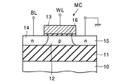
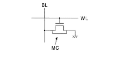
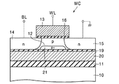
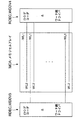
[基本コンセプト]
図1は後述する各実施の形態によるDRAMの単位メモリセルMCの基本断面構造を示し、図2はその等価回路を示している。メモリセルMCは、SOI構造のNチャネルMISトランジスタにより構成されている。即ち、シリコン基板10上に絶縁膜としてシリコン酸化膜11が形成され、このシリコン酸化膜11上にp型シリコン層12が形成されたSOI基板が用いられている。この基板のシリコン層12上に、ゲート酸化膜16を介してゲート電極13が形成され、ゲート電極13に自己整合されてn型ソース、ドレイン拡散層14,15が形成されている。
【0010】
ソース、ドレイン14,15は、底部のシリコン酸化膜11に達する深さに形成されている。従って、p型シリコン層12からなるチャネルボディは、チャネル幅方向(図の紙面に直交する方向)の分離を酸化膜で行うとすれば、底面及びチャネル幅方向の側面が他から絶縁分離され、チャネル長方向はpn接合分離されたフローティング状態になる。
【0011】
このメモリセルMCをマトリクス配列する場合、ゲート13はワード線WLに接続され、ソース15は固定電位線(接地電位線)に接続され、ドレイン14はビット線BLに接続される。
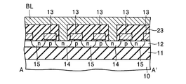
【0012】
図3は、メモリセルアレイのレイアウトを示し、図4A及び図4Bはそれぞれ図3のA−A’,B−B’断面を示している。p型シリコン層12は、シリコン酸化膜22の埋め込みにより、格子状にパターン形成される。即ちドレインを共有する二つのトランジスタの領域がワード線WL方向にシリコン酸化膜22により素子分離されて配列される。或いはシリコン酸化膜22の埋め込みに代わって、シリコン層12をエッチングすることにより、横方向の素子分離を行っても良い。ゲート13は一方向に連続的に形成されて、これがワード線WLとなる。ソース15は、ワード線WL方向に連続的に形成されて、これが固定電位線(共通ソース線)となる。
【0013】
トランジスタ上は層間絶縁膜23で覆われこの上にビット線BLが形成される。ビット線BLは、二つのトランジスタで共有するドレイン14にコンタクトして、ワード線WLと交差するように配設される。なおソース15の固定電位線(共通ソース線)の配線抵抗を低下させるために、ビット線BLの上又は下に、ワード線WLと平行な金属配線を形成し、これを複数のビツト線毎に固定電位線に接続するようにしてもよい。
【0014】
これにより、各トランジスタのチャネルボディであるシリコン層12は、底面及びチャネル幅方向の側面が酸化膜により互いに分離され、チャネル長方向にはpn接合により互いに分離されてフローティング状態に保たれる。
【0015】
そしてこのメモリセルアレイ構成では、ワード線WLおよびビット線BLを最小加工寸法Fのピッチで形成したとして、単位セル面積は、図3に破線で示したように、2F×2F=4F2となる。
【0016】
このnチャネル型MISトランジスタからなるメモリセルMCの動作原理は、MISトランジスタのチャネルボディ(他から絶縁分離されたp型シリコン層12)の多数キャリアであるホールの蓄積を利用する。即ち、トランジスタを5極管領域で動作させることにより、ドレイン14から大きな電流を流し、ドレイン14の近傍でインパクトイオン化を起こす。このインパクトイオン化により生成される多数キャリアであるホールをp型シリコン層12に保持させ、そのホール蓄積状態を例えばデータ“1”とする。ドレイン14とp型シリコン層12の間のpn接合を順方向バイアスして、p型シリコン層12の過剰ホールをドレイン側に放出した状態をデータ“0”とする。
【0017】
データ“0”,“1”は、チャネルボディの電位の差として、従ってトランジスタのしきい値電圧の差として記憶される。即ち、ホール蓄積によりチャネルボディの電位が高いデータ“1”状態のしきい値電圧Vth1は、データ“0”状態のしきい値電圧Vth0より低い。ボデイに多数キャリアであるホールを蓄積した“1”データ状態を保持するためには、ワード線には負のバイアス電圧を印加することが必要になる。このデータ保持状態は、理論上、リニア領域で読み出し動作を行っている限り、且つ、逆データの書き込み動作(消去)を行わない限り、読み出し動作を行っても変わない。即ち、キャパシタの電荷蓄積を利用する1トランジスタ/1キャパシタのDRAMと異なり、非破壊読み出しが可能である。
【0018】
データ読み出しの方式には、いくつか考えられる。ワード線電位Vwlとチャネルボディ電位VBの関係は、データ“0”,“1”との関係で図5のようになる。従ってデータ読み出しの第1の方法は、ワード線WLにデータ“0”,“1”のしきい値電圧Vth0,Vth1の中間になる読み出し電位を与えて、“0”データのメモリセルでは電流が流れず、“1”データのメモリセルでは電流が流れることを利用する。具体的には例えば、ビット線BLを所定の電位VBLにプリチャージして、その後ワード線WLを駆動する。これにより、図6に示すように、“0”データの場合、ビット線プリチャージ電位VBLの変化がなく、“1”データの場合はプリチャージ電位VBLが低下する。
【0019】
第2の読み出し方式は、ワード線WLを立ち上げてから、ビット線BLに電流を供給して、“0”,“1”の導通度に応じてビット線電位の上昇速度が異なることを利用する。簡単には、ビット線BLを0Vにプリチャージし、図7に示すようにワード線WLを立ち上げて、ビット線電流を供給する。このとき、ビット線の電位上昇の差をダミーセルを利用して検出することにより、データ判別が可能となる。
【0020】
第3の読み出し方式は、ビット線BLを所定の電位にクランプしたときの、“0”,“1”で異なるビット線電流の差を読む方式である。電流差を読み出すには、電流−電圧変換回路が必要であるが、最終的には電位差を差動増幅して、センス出力を出す。
【0021】
この発明において、選択的に“0”データを書き込むためには、即ちメモリセルアレイのなかで選択されたワード線WLとビット線BLの電位により選択されたメモリセルのチャネルボディのみからホールを放出させるには、ワード線WLとチャネルボディの間の容量結合が本質的になる。データ“1”でチャネルボディにホールが蓄積された状態は、ワード線を十分負方向にバイアスして、メモリセルのゲート・チャネルボディ間容量が、ゲート酸化膜容量となる状態(即ち表面に空乏層が形成されていない状態)で保持することが必要である。
【0022】
また、書き込み動作は、“0”,“1”共に、パルス書き込みとして消費電力を減らすことが好ましい。“0”書き込み時、選択トランジスタのチャネルボディからドレインにホール電流が、ドレインからチャネルボディに電子電流が流れるが、チャネルボディにホールが注入されることはない。
【0023】
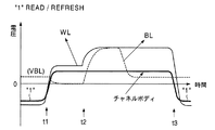
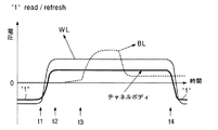
より具体的な動作波形を説明する。図8〜図11は、選択セルによるビット線の放電の有無によりデータ判別を行う第1の読み出し方式を用いた場合のリード/リフレッシュ及びリード/ライトの動作波形である。
【0024】
図8及び図9は、それぞれ“1”データ及び“0”データのリード/リフレッシュ動作である。時刻t1までは、データ保持状態(非選択状態)であり、ワード線WLには負電位が与えられている。時刻t1でワード線WLを正の所定電位に立ち上げる。このときワード線電位は、“0”,“1”データのしきい値Vth0,Vth1の間に設定する。これにより、“1”データの場合、予めプリチャージされていたビット線VBLは放電により低電位になる。“0”データの場合はビット線電位VBLは保持される。これにより“1”,“0”データが判別される。
【0025】
そして、時刻t2で、ワード線WLの電位を更に高くし、同時に読み出しデータが“1”の場合には、ビット線BLに正電位を与え(図8)、読み出しデータが“0”の場合はビット線BLに負電位を与える(図9)。これにより、選択メモリセルが“1”データの場合、5極管動作により大きなチャネル電流が流れてインパクトイオン化が起こり、チャネルボディに過剰のホールが注入保持されて再度“1”データが書き込まれる。“0”データの場合には、ドレイン接合が順方向バイアスになり、チャネルボディに過剰ホールが保持されていない“0”データが再度書き込まれる。
【0026】
そして、時刻t3でワード線WLを負方向にバイアスして、リード/リフレッシュ動作を終了する。“1”データ読み出しを行ったメモリセルと同じビット線BLにつながる他の非選択メモリセルでは、ワード線WLが負電位、従ってチャネルボディが負電位に保持されて、インパクトイオン化は起こらない。“0”データ読み出しを行ったメモリセルと同じビット線BLにつながる他の非選択メモリセルでは、やはりワード線WLが負電位に保持されて、ホール放出は起こらない。
【0027】
図10及び図11は、同じ読み出し方式によるそれぞれ“1”データ及び“0”データのリード/ライト動作である。図10及び図11での時刻t1での読み出し動作はそれぞれ、図8及び図9と同様である。読み出し後、時刻t2でワード線WLを更に高電位とし、同じ選択セルに“0”データを書き込む場合には同時に、ビット線BLに負電位を与え(図10)、“1”データを書き込む場合にはビット線BLに正電位を与える(図11)。これにより、“0”データが与えられたセルでは、ドレイン接合が順方向バイアスになり、チャネルボディのホールが放出される。“1”データが与えられたセルでは、ドレイン近傍でインパクトイオン化が起こり、チャネルボディに過剰ホールが注入保持される。
【0028】
図12〜図15は、ビット線BLを0Vにプリチャージし、ワード線選択後にビット線BLに電流を供給して、ビット線BLの電位上昇速度によりデータ判別を行う第2の読み出し方式を用いた場合のリード/リフレッシュ及びリード/ライトの動作波形である。
【0029】
図12及び図13は、それぞれ“1”データ及び“0”データのリード/リフレッシュ動作である。負電位に保持されていたワード線WLを、時刻t1で正電位に立ち上げる。このときワード線電位は、図7に示したように、“0”,“1”データのしきい値Vth0,Vth1のいずれよりも高い値に設定する。或いは・ワード線電位を、第1の読み出し方式と同様に、“0”,“1”データのしきい値Vth0,Vth1の間に設定してもよい。そして、時刻t2でビット線に電流を供給する。これにより、“1”データの場合、メモリセルが深くオンしてビット線BLの電位上昇は小さく(図12)、“0”データの場合メモリセルの電流が小さく(或いは電流が流れず)、ビット線電位は急速に上昇する。これにより“1”,“0”データが判別される。
【0030】
そして、時刻t3で・読み出しデータが“1”の場合には、ビット線BLに正の電位を与え(図12)、読み出しデータが“0”の場合はビット線BLに負の電位を与える(図13)。これにより、選択メモリセルが“1”データの場合、ドレイン電流が流れてインパクトイオン化が起こり、チャネルボディに過剰ホールが注入保持されて再度“1”データが書き込まれる。“0”データの場合には、ドレイン接合が順方向バイアスになり、チャネルボディに過剰ホールのない“0”データが再度書き込まれる。
【0031】
時刻t4でワード線WLを負方向にバイアスして、リード/リフレッシュ動作を終了する。
【0032】
図14及び図15は、同じ読み出し方式によるそれぞれ“1”データ及び“0”データのリード/ライト動作である。図14及び図15での時刻t1及びt2での読み出し動作はそれぞれ、図12及び図13と同様である。読み出し後、同じ選択セルに“0”データを書き込む場合には、ビット線BLに負電位を与え(図14)、“1”データを書き込む場合にはビット線BLに正電位を与える(図15)。これにより、“0”データが与えられたセルでは、ドレイン接合が順方向バイアスになり、チャネルボディの過剰ホールが放出される。“1”データが与えられたセルでは、大きなドレイン電流が流れてドレイン近傍でインパクトイオン化が起こり、チャネルボディに過剰ホールが注入保持される。
【0033】
以上のようにこの発明によるメモリセルMCは、他から電気的に分離されたフローティングのチャネルボディを持つ単純なMISトランジスタにより構成され、4F2のセルサイズが実現可能である。また、フローティングのチャネルボディの電位制御は、ゲート電極からの容量結合を利用しており、ソースも固定電位である。即ち、読み出し/書き込みの制御は、ワード線WLとビット線BLで行われ、簡単である。更にメモリセルMCは基本的に非破壊読み出しであるので、センスアンプをビット線毎に設ける必要がなく、センスアンプのレイアウトは容易になる。更に電流読み出し方式であるので、ノイズにも強く、例えばオープンビット線方式でも読み出しが可能である。また、メモリセルの製造プロセスも簡単である。
【0034】
また、SOI構造は、今後のロジックLSIの性能向上を考えたときに重要な技術となる。この発明によるDRAMは、この様なSOI構造のロジックLSIとの混載を行う場合にも非常に有望である。キャパシタを用いる従来のDRAMと異なり、ロジックLSIのプロセスと異なるプロセスを必要とせず、製造工程が簡単になるからである。
【0035】
更に、この発明によるSOI構造のDRAMは、従来の1トランジスタ/1キャパシタ型のDRAMをSOI構造とした場合に比べて、優れた記憶保持特性が得られるという利点がある。即ち従来の1トランジスタ/1キャパシタ型のDRAMをSOI構造とすると、フローティングのチャネルボディにホールが蓄積されてトランジスタのしきい値が下がり、トランジスタのサブスレッショルド電流が増加する。これは記憶保持特性を劣化させる。これに対してこの発明による1トランジスタのみのメモリセルでは、記憶電荷を減少させるトランジスタパスは存在せず、データ保持特性は純粋にpn接合のリークのみで決まり、サブスレッショルドリークという問題がなくなる。
【0036】
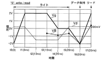
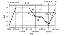
ここまでに説明した基本的なメモリセルにおいて、チャネルボディの電位の差として記憶されるデータ“0”,“1”のしきい値電圧差をどれだけ大きくとれるかがメモリ特性にとって重要になる。この点に関してシミュレーションを行った結果によると、ゲートからの容量結合によるチャネルボディの電位制御を伴うデータ書き込みに際して、書き込み直後の“0”,“1”データのチャネルボデイ電位差に比べて、その後のデータ保持状態での“0”,“1”データのチャネルボディ電位差が小さくなることが明らかになった。そのシミュレーション結果を次に説明する。
【0037】
デバイス条件は、ゲート長Lg=0.35μm、p型シリコン層12は厚さがtSi=100nm、アクセプタ濃度がNA=5×10¹⁷/cm3であり、ソース14及びドレイン15のドナー濃度がND=5×1020/cm3、ゲート酸化膜厚がtox=10nmである。
【0038】
図16は、“0”データ書き込みと、その後のデータ保持及びデータ読み出し(それぞれ瞬時で示している)におけるゲート電位Vg、ドレイン電位Vd、及びチャネルボディの電位VBを示している。図17は同じく、“1”データ書き込みと、その後のデータ保持及びデータ読み出し(それぞれ瞬時で示している)におけるゲート電圧Vg、ドレイン電圧Vd、及びチャネルボディ電圧VBを示している。
【0039】
また、時刻t6−t7のデータ読み出し動作における“0”データのしきい値電圧Vth0と“1”データのしきい値電圧Vth1を見るために、その時間のドレイン電流Idsとゲート・ソース間電圧Vgsを描くと、図18のようになる。但し、チャネル幅Wとチャネル長LをW/L=0.175μm/0.35μmとし、ドレイン・ソース間電圧をVds=0.2Vとしている。
【0040】
図18から、“0”書き込みセルのしきい値電圧Vth0と“1”書き込みセルのしきい値電圧Vth1の差ΔVthは、ΔVth=0.32Vとなっている。以上の解析結果から、問題になるのは、図16及び図17において、“0”書き込み直後(時刻t3)のチャネルボディ電位がVB=−0.77V、“1”書き込み直後のチャネルボディ電位がVB=0.85Vであり、その差が1.62Vであるのに対し、データ保持状態(時刻t6)では、“0”書き込みセルのチャネルボディ電位がVB=−2.04V、“1”書き込みセルのボデイ電位がVB=−1.6Vであり、その差が0.44Vと書き込み直後より小さくなっていることである。
【0041】
このように書き込み直後に比べて、その後のデータ保持状態でのチャネルボディ電位のデータによる差が小さくなる要因は、二つ考えられる。
【0042】
その一つは、ゲートからチャネルボディヘの容量カップリングがデータにより異なることである。“0”書き込み直後(t3−t4)では、ドレインは−1.5Vであるが、“1”書き込み直後ではドレインが2Vである。従って、その後ゲート電位Vgを下げたとき、“1”書き込みセルではチャネルが容易に消失し、ゲート・チャネルボディ間の容量が顕在化して、次第にチャネルボディにホールが蓄積されて容量が大きくなる。一方、“0”書き込みセルではチャネルが容易には消失せず、ゲート・チャネルボディ間容量が顕在化しない。
【0043】
ゲート電位を下げ始めるより先にドレイン電位を200mVにリセットすれば、上述したアンバランスは解消されるかに思われる。しかしこの場合には、“0”書き込みを行ったセルでは、チャネルが形成された状態でドレイン電位が上昇して3極管動作による電流が流れる。そして、“0”書き込みにより折角下げたチャネルボディ電位が、n型のドレイン及びチャネル反転層とp型のチャネルボディとの間の容量結合により上昇してしまい、好ましくない。
【0044】
もう一つは、書き込み後の時刻t4−t5の間で、ソース或いはドレインとチャネルボディとの間のpn接合の容量でチャネルボディ電位が影響され、これが“0”,“1”データの信号量を減らす方向に作用することである。
【0045】
そこで、上記基本メモリセルに対して、チャネル形成の制御を行うためのゲート(第1のゲート)とは別に、チャネルボディを容量結合により電位制御するためのゲート(第2のゲート)を付加する。第2のゲートとチャネルボディとの間の容量を確保するために、第2のゲート側の表面には、チャネル反転層が形成されることなく、蓄積状態(アキュミュレーション状態)を保つように、チャネルボディと同じ導電型の高濃度領域を形成する。そして、第2のゲートは、例えば第1のゲートより低い電位で、或いは同じ電位で第1のゲートと同期して駆動する。或いはまた第2のゲートは例えば、ソースに与えられる基準電位或いはそれより低い電位(nチャネルの場合であれば、負電位)に固定してもよい。
【0046】
以下に具体的な実施の形態を説明する。
【0047】
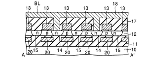
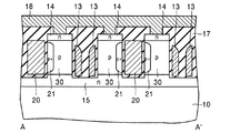
[実施の形態1]
図19Aは、この発明の実施の形態1によるメモリセルMCの構造を、図1に対応させて示している。基本構造は、図1と同様であり、図1と異なる点は、チャネル制御を行う第1のゲート13とは別に、シリコン層12にゲート絶縁膜19を介して対向して容量結合する第2のゲート20が酸化膜11に埋め込まれている点、及びシリコン層12の第2のゲート20側の表面には、チャネル反転層が形成されない程度の高濃度のp+型層21を形成している点である。すなわち、シリコン層12には、このシリコン層12と同じ導電型で、且つ、シリコン層12の不純物濃度よりも高い不純物濃度を有する、p+型層21が形成されている。このp+型層21が存在することにより、第1のゲート13と第2のゲート20に正の電位を印加して書き込みを行う場合でも、第1のゲート13側のチャネルボディにはチャネルが形成されるが、第2のゲート20側のチャネルボディにはチャネルが形成されにようになる。
【0048】
なお、この実施の形態のメモリセルMCにおいては、ゲート絶縁膜19は、第1のゲート13側のゲート絶縁膜16と同じ膜厚としている。
【0049】
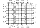
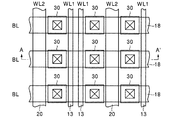
実際のメモリセルアレイ構成では、図19Aに示すメモリセルMCが複数個マトリクス配列され、第1のゲート13は第1のワード線WL1として連続的に形成され、第2のゲート20はこれと並行する第2のワード線WL2として配設される。
【0050】
図19Bは、この様なメモリセルMCを複数、マトリクス配列したメモリセルアレイの等価回路を示している。一方向に並ぶ複数のメモリセルMCの第1のゲート(G1)13は、第1のワード線WL1に接続され、第2のゲート(G2)20は、第2のワード線WL2に接続される。これらのワード線WL1,WL2と交差する方向に、メモリセルMCのドレインが接続されるビット線BLが配設される。全メモリセルMCのソース15は固定電位線(接地電位線VSS)に接続される。
【0051】
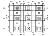
図19Cは、メモリセルアレイのレイアウトを示し、図19D、図19Eはそれぞれ図19CのA−A’,B−B’線断面を示している。p型シリコン層12は、シリコン酸化膜22の埋め込みにより、格子状にパターン形成される。即ちドレイン14を共有する二つのトランジスタの領域がワード線WL1,WL2の方向にシリコン酸化膜22により素子分離されて配列される。或いはシリコン酸化膜22の埋め込みに代わって、シリコン層12をエッチングすることにより、横方向の素子分離を行っても良い。第1のゲート13及び第2のゲート20は、一方向に連続的に形成されて、これらがワード線WL1及びWL2となる。ソース15は、ワード線WL1,WL2の方向に連続的に形成されて、これが固定電位線(共通ソース線)となる。トランジスタ上は層間絶縁膜17で覆われこの上にビット線(BL)18が形成される。ビット線18は、二つのトランジスタで共有するドレイン14にコンタクトして、ワード線WL1,WL2と交差するように配設される。
【0052】
これにより、各トランジスタのチャネルボディであるシリコン層12は、底面及びチャネル幅方向の側面が酸化膜により互いに分離され、チャネル長方向にはpn接合により互いに分離されて、フローティング状態に保たれる。
【0053】
そしてこのメモリセルアレイ構成では、ワード線WL1,WL2およびビット線BLを最小加工寸法Fのピッチで形成したとして、単位セル面積は、図19Cに破線で示したように、2F×2F=4F2となる。
【0054】
この様な構成として、先に基本メモリセルを用いて説明したと同様の動作を行う。このとき、第2のワード線WL2は、第1のワード線WL1と同期して、第1のワード線WL1より低い電位で駆動するものする。この様に、第2のゲート20を第1のゲート13と共に駆動することにより、しきい値電圧差の大きい“0”,“1”データ書き込みができる。即ち、第2のゲート20をデータ保持状態では負電位にして、“1”データの蓄積状態を良好に保持しながら、データ書き込み時にその電位を上昇させることにより、容量結合によりチャネルボディ電位を上昇させて、データ書き込みを確実にすることができる。
【0055】
すなわち、“0”データ書き込みの場合に、第1のゲート13に正の電位を印加するが、そうすると、チャネルボディの第1のゲート13側にチャネル反転層が形成される。しかし、チャネル反転層が形成されると、このチャネル反転層が阻害要因となり、第1のゲート13によるチャネルボディへの容量結合が弱くなる。このため、第1のゲート13に正の電位を印加してもチャネルボディの電位を十分に上昇させることができなくなってしまう。
【0056】
しかし、この実施の形態では、第2のゲート20にも正の電位を印加することにより、チャネルボディの電位を十分に上昇させることができる。なぜなら、p+型層21が形成されているため、チャネルボディの第2のゲート20側にはチャネル反転層が形成されず、したがって、第2のゲート20に正の電位を印加することにより、容量結合でチャネルボディの電位を十分に上昇させることができるのである。このため、的確な“0”データ書き込みが可能である。
【0057】
また、非選択の第1のワード線WL1の電位を下げることでデータ保持を行うが、このとき対をなす第2のワード線WL2の電位も下げてチャネルボディ電位を低く制御することにより、同じビット線に接続された他のセルで“0”データ書き込みを行う場合に、“1”データを保持する非選択セルでのデータ破壊が確実に防止される。更に、“1”書き込みビット線に接続される非選択の“0”データセルでは、表面ブレークダウンやGIDL電流によるデータ破壊の懸念があるが、この実施の形態の場合、第2のワード線によりチャネルボディ電位を下げることで、これらの懸念も解消される。
【0058】
更に、“0”書き込み時、ビット線の電位を大きく下げると、ソースからビット線に電流が流れるが、この実施の形態の場合、第2のゲート20によりチャネルボディ電位を上昇せしめるため、ビット線電位をそれほど下げる必要がない。例えばビット線電位をソースの基準電位と同じ程度として、ソースからビット線に流れる電流を抑制することが可能である。
【0059】
またデータ読み出し時は、誤まって“1”書き込みにならないように、3極管動作させることが必要である。このため、ビット線電位は“1”書き込み時より低いが、このためドレインとチャネルボディ間の空乏層の伸びは、“1”書き込み時より小さく、従ってビット線とチャネルボディの容量結合が大きくなる。このことは、書き込み時にチャネルボディに注入されたキャリアが容量再分配されて、チャネルボディ電位の低下の原因となる。この実施の形態においては、第2のゲート20による制御によって、チャネルボディの多数キャリア蓄積状態を良好に保持することができる。
【0060】
なお、上の説明では、第1のゲート13に対して第2のゲート20を低い電位で駆動するようにしたが、第2のゲート20側のチャネルボディ表面にはp+型層21を形成しているため、第2のゲート20を第1のゲート13と同じ電位で駆動してもチャネル反転層が形成されることはなく、チャネルボディに対して大きな容量結合で電位制御することができる。
【0061】
また、第1のゲート13側のゲート絶縁膜16と第2のゲート20側のゲート絶縁膜19は、厚みが同じでなくてもよく、必要とする容量結合の大きさに応じてそれぞれ最適設定することができる。
【0062】
また、この実施の形態では、第1のゲート13と第2のゲート20をシリコン層の上下面に対向させたが、同じ面に対向させるようにしてもよい。具体的には、第1のゲートと第2のゲートを一体として配設し、チャネル領域の一部にチャネル反転層の形成を防止する高濃度領域を形成することにより、上記実施の形態と同様の動作が可能になる。第1のゲートと第2のゲートをシリコン層の同じ面に別々に配置することもできる。
【0063】
図19Fは、第1のゲート13と第2のゲート20を一体にしたメモリセルMCの構成を示す斜視図であり、図19Gは、図19FのA−A’断面を示しており、図19Hは、図19FのB−B’断面を示している。
【0064】
これらの図から分かるように、この例では、第2のゲート20は形成されておらず、第1のゲート13が第2のゲート20と同様の役割を果たすようにしている。このために、シリコン層12の表面側半分の領域に、高濃度のp+型層21が形成されている。すなわち、この例では、シリコン層12が不純物濃度の低いp−型の領域として形成されており、p+型層21がこれよりも不純物濃度が高いp+型の領域として形成されている。
【0065】
p+型層21は、その平面視において、シリコン層12のおよそ半分の領域に形成されている。p+型層21の深さは、ゲート絶縁膜16と酸化膜11との間の位置まで形成されている。あるいは、酸化膜11まで届いても構わない。このp+型層21を形成する大きさは任意であり、第1のゲート13を駆動した場合にチャネル反転層が形成されないようにして、チャネルボディに対して大きな容量結合で電位制御できればよい。
【0066】
図19Iは、図19Fに示したメモリセルMCをマトリクス状に配置したメモリセルアレイのレイアウトを示す図であり、図19Cに対応する図である。図19Jは、図19IのA−A’断面を示す図であり、図19Kは、図19IのB−B’断面を示す図であり、図19Lは、図19IのC−C’断面を示す図である。
【0067】
これらの図から分かるように、ゲート13は一方向に連続的に形成されて、1つのワード線WLとなる。但し、この例では、上述した第2のゲート20が存在しないので、第2のワード線WL2は形成されていない。ビット線18は、二つのトランジスタで共有するドレイン14にコンタクトして、ワード線WLと交差するように配設される。そして、ドレイン14及びソース15の間のチャネルボディにおけるワード線WL側の一部に、p+型層21が形成される。
【0068】
なお、このメモリセルMCにおいては、図19Hに示すように、p+型層21は、そのB−B’断面方向において、ドレイン領域14とソース領域15に接するように形成されている。但し、必ずしもp+型層21は、ドレイン領域14とソース領域15に接していなくともよい。
【0069】
そのような例を、図19M及び図19Nに示す。図19Mは、メモリセルMCの構成を示す斜視図であり、図19Fに対応する図である。図19Nは、図19MにおけるB−B’断面を示す図であり、図19Hに対応する図である。図19MにおけるA−A’断面は、先に示した図19Gと同様である。
【0070】
これら図19M及び図19Nに示すように、p+型層21は、ドレイン領域14とソース領域15と接していない。このようにすることにより、このメモリセルMCのリテンション時間が短くなってしまうのを、回避することができる。より詳しく説明すると、p+型層21とn型のドレイン領域14とソース領域15とが直接的に接すると、pn接合に逆バイアスが印加された場合の空乏層の延びが小さくなってしまう。すると、電界の強さが大きくなり、pn接合部分のリーク電流が増加してしまい、メモリセルMCがデータを保持することのできる時間であるリテンション時間が短くなってしまうのである。
【0071】
これに対して、図19M及び図19Nに示すように、p+型層21をドレイン領域14とソース領域15と接しないように形成することにより、このような事態を回避することができる。つまり、p+型層21がドレイン領域14とソース領域15と接する場合と比べて、メモリセルMCのリテンション時間を長くすることができるのである。
【0072】
[実施の形態2]
図20は、実施の形態2によるメモリセルMCの構造である。図19Aの実施の形態と異なりこの実施の形態では、第2のゲート20は、配線としてパターニングされず、セルアレイ領域全体をカバーするように共通のゲート(バックプレート)として配設される。すなわち、第2のゲート20は、このメモリセルアレイ内にあるすべてのMISトランジスタに共通に設けられている。この様な構造とすれば、第2のゲート20と第1のゲート13の位置合わせが不要であり、製造プロセスが簡単になる。
【0073】
この様な構成として、第2のゲート20を例えばソース電位或いはそれより低い電位に固定して、先の基本メモリセルで説明したと同様の動作を行う。この場合にも、第1のゲート13(ワード線WL)の振幅を大きくすることにより、“0”,“1”データの信号差を大きくすることができる。即ち、第2のゲート20を固定電位でチャネルボディに容量結合させると、第1のゲート13からのチャネルボディに対する容量結合は基本メモリセルの場合に比べて容量分割により小さくなる。しかしその分、第1のゲート13の駆動振幅を上げることによって、第1のゲート13によるチャネルボディの電位を、“0”,“1”データについて大きな差のない状態で制御することができ、データ保持状態で“0”,“1”データのしきい値電圧差を大きくすることが可能になる。
【0074】
[実施の形態3]
図21は、実施の形態3によるメモリセルアレイのレイアウトを示し、図22はそのA−A’断面を示している。ここまでの実施の形態では、フローティングのチャネルボディを持つトランジスタを作るためにSOI基板を用いたのに対し、この実施の形態では、いわゆるSGT(Surrounding Gate Transistor)構造を利用して、フローティングのチャネルボディを持つ縦型MISトランジスタによりメモリセルを構成する。
【0075】
シリコン基板10には、RIEにより、縦横に走る溝を加工して、p型柱状シリコン30が配列形成される。これらの各柱状シリコン30の両側面に対向するように、第1のゲート13と第2のゲート20が形成される。第1のゲート13と第2のゲート20は、図22の断面において、柱状シリコン30の間に交互に埋め込まれる。第1のゲート13は、側壁残しの技術により、隣接する柱状シリコン30の間で隣接する柱状シリコン30に対して独立したゲート電極として分離形成される。一方第2のゲート20は、隣接する柱状シリコン30の間にこれらが共有するように埋め込まれる。第1,第2のゲート13,20はそれぞれ、第1,第2のワード線WL1,WL2として連続的にパターン形成される。
【0076】
柱状シリコン30の上面にn型ドレイン拡散層14が形成され、下部には全セルで共有されるn型ソース拡散層15が形成される。また柱状シリコン層30の第2のゲート20側の側面には、p+型層21が形成される。これにより、各チャネルボディがフローティングである縦型トランジスタからなるメモリセルMCが構成される。ゲート13,20が埋め込まれた基板には層間絶縁膜17が形成され、この上にビット線18が配設される。
【0077】
この実施の形態によっても、先の各実施の形態と同様の動作ができる。この実施の形態によれば、SOI基板を用いる必要がなく、従ってメモリセルのみ縦型トランジスタによるフローティングのチャネルボディを持たせ、セルアレイ以外のセンスアンプ、トランスファゲート、ロウ/カラムデコーダ等の周辺回路は通常の平面型トランジスタを用いることができる。このため、SOI基板を用いた場合のように、チャネルボディ浮遊効果による回路の不安定性がなくすために周辺回路トランジスタのチャネルボディ電位を固定するためのコンタクトを形成するという必要がなく、それだけ周辺回路部の面積縮小が可能になる。
【0078】
[実施の形態4]
図23及び図24は、実施の形態3と同様のSGT構造を用いた実施の形態のセルアレイのレイアウトとそのA−A’断面を、図21及び図22に対応させて示している。実施の形態3との相違は、ゲート13と20とが一体に柱状シリコン層30の周囲を取り巻いて、共通のワード線WLとして配設されていることである。柱状シリコン層30のゲート20が対向する側面には、実施の形態3と同様に、p+型層21が形成されている。
【0079】
この実施の形態の場合、ゲート13,20は、ワード線WLとして一体に同電位で駆動されることになる。ゲート20側はp+型層21があるためにチャネル反転層が形成されることはなく、従ってワード線WLは大きな容量でチャネルボディに結合して、その電位を制御することができる。このp+型層21が形成される面は、柱状シリコン層30の1つの面に限られるものではなく、2つの面、3つの面に形成するようにしてもよい。つまり、p+型層21は、柱状シリコン層30の一つ以上の面に形成されていればよい。
【0080】
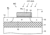
[実施の形態5]
図25Aは、“0”データ書き込みの信頼性の改善を可能とした実施の形態のメモリセルMCの構造を、図1に対応させて示す。この実施の形態のメモリセル構造が図1と異なる点は、ゲート13がドレイン14に対してオフセットを持つようにしていることである。すなわち、チャネルボディ側のソース15上には、ゲート絶縁膜16を介して、ゲート13が形成されている。つまり、ゲート13のソース15に対する重なり量は正である。これに対して、ドレイン14上には、ゲート13が形成されていない。つまり、ゲート13のドレイン14に対する重なり量は負である。
【0081】
これは、図25Aに示したように、ドレイン14及びソース15のイオン注入を斜めイオン注入とすることにより、容易に実現することができる。或いは斜めイオン注入によらず、ドレイン側のゲート側壁にのみ側壁絶縁膜を形成した状態で通常のイオン注入を行うことによっても、同様のオフセット構造を得ることができる。その他は、図1と変わらない。
【0082】
上述した実施の形態におけるメモリセルでは、“0”書き込みは、ドレイン領域14とチャネルボデイの間に順バイアスを与えて、チャネルボディの多数キャリアをドレイン領域14に放出させる。この場合、図1に示した通常のトランジスタ構造では、チャネル反転層が形成されてこれがゲート13とチャネルボディの間のシールド層となり、チャネル反転層とチャネルボディとの間の容量結合が大きくなる。この結果、ドレイン領域14を負電位から0Vに戻すときに、チャネル反転層とチャネルボディの容量結合によりチャネルボディ電位が上昇し、十分に“0”書き込みができなくなる可能性がある。また、チャネル反転層のためにゲート13とチャネルボディの間の容量が小さくなるため、ビット線の影響をより大きく受けやすくなる。更にチャネル反転層が形成されると、チャネル電流(nチャネルの場合電子電流)が流れる。このチャネル電流は、書き込み動作には無用の電流であり、書き込み電力の増大を招くだけでなく、もしインパクトイオン化が生じれば、“1”書き込みモードとなり、“0”書き込みの信頼性が低下する。
【0083】
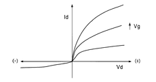
これに対して、図25Aに示すように、ドレイン側にオフセット構造を持たせると、ドレイン領域14に正電位が与えられてドレイン接合が逆バイアスとなる通常のトランジスタ動作の場合は、図25Bに示すように、ドレイン領域14から拡がる空乏層DLがゲート13直下まで延びる。このため、ゲート13に正の電圧を印加することにより、ドレイン領域14からの空乏層DLとソース領域15との間にチャネル反転層CHが形成され、ドレイン領域14とソース領域15との間にチャネル電流が流れる状態になる。つまり、図25Aに示すメモリセルMCは、図26に示すように、MISトランジスタとして、正常動作する。この図26は、ドレイン領域14に印加される電圧Vdと、ソース/ドレイン間を流れる電流Idとの関係を示すグラフを示している。そして、ゲート13に印加される電圧Vgを変化させた場合の特性を示している。
【0084】
しかし、ドレイン領域14に負電位が与えられた場合には、トランジスタ動作としてはドレイン,ソースの機能が逆となり、図25Cに示すように、空乏層DLはソース領域15側に形成されるとともに、チャネル反転層CHがソース領域14から離れて形成される。このため、図26に示すように、ドレイン領域14とソース領域15との間にチャネル電流が殆ど流れない。
【0085】
従ってこの実施の形態によると、“0”書き込み時(つまり、図25Cに示すように、ドレイン領域14とチャネルボディとの間に順バイアスを与えた時)、ドレイン領域14とチャネルボディとの無用な容量結合によるチャネルボディ電位の上昇が抑えられ、“0”書き込みマージンを上げることができる。また“0”書き込み時に無用なチャネル電流を抑えて、ビット線BLに流れる書き込み電流を低減し、書き込み電力を低減することができる。
【0086】
上では、逆方向について殆ど電流が流れない場合について述べたが、チャネル電流に10%以上の差がつく軽い非対称性を持たせることで、同様に電流低減等の効果が得られる。また、ドレイン領域14側にオフセットを持たせるのは、ソース、ドレイン逆転時のチャネル電流を非対称とする手段の一つであり、ソース、ドレインの順逆時のチャネル電流に非対称を与えるために他の手法を用いることもできる。すなわち、MISトランジスタが、ソース領域15からドレイン領域14へチャネル電流が流れる場合と、ドレイン領域14からソース領域15へチャネル電流が流れる場合とで、同じ電位をゲート13に与えた場合でも異なる特性を有するようにすればよい。
【0087】
[実施の形態6]
図27及び図28はそれぞれ、図19A及び図20のメモリセルMCについて、同様にゲートオフセット構造を導入した実施の形態を示している。この実施の形態によっても同様に、“0”書き込み時の無用な電流を低減することができる。
【0088】
図29A及び図29Bは、SGT構造を用いたメモリセルMCについて、同様にゲートオフセット構造を導入した実施の形態を示している。図29Aは、そのようなメモリセルMCにより構成されたメモリセルアレイのレイアウトを示す平面図であり、図29Bは、図29AのA−A’断面を示す図である。これら図29A及び図29Bに示すように、ゲート13は柱状シリコン層30を取り巻く一体のものである。また、柱状シリコン30には、p+型層21の高濃度領域は形成されていない。
【0089】
図29Bに示すように、柱状シリコン層30におけるチャネルボディ側のソース15の周囲には、ゲート絶縁膜を介して、ゲート13が形成されている。つまり、ゲート13のソース15に対する重なり量は正である。これに対して、柱状シリコン層30におけるドレイン14の周囲には、ゲート13が形成されていない。つまり、ゲート13のドレイン14に対する重なり量は負である。
【0090】
図30Aは、図21及び図22の実施の形態3において、ゲートオフセット構造を導入したメモリセルで構成されたメモリセルアレイのレイアウトを示す平面図である。図30Bは、図30AにおけるA−A’断面を示す図である。これら図30A及び図30Bに示すように、第1のゲート13は、ソース領域15側にシフトして形成されている。すなわち、柱状シリコン層30におけるソース15の側面には、ゲート絶縁膜を介して、第1のゲート13が形成されている。つまり、第1のゲート13のソース15に対する重なり量は正である。これに対して、柱状シリコン層30におけるドレイン14の側面には、第1のゲート13が形成されていない。つまり、第1のゲート13のドレイン14に対する重なり量は負である。それ以外の構成は、上述した実施の形態3と同様であり、第1のゲート13と第2のゲート20は、別々のワード線として配設されている。
【0091】
図30Cは、図23及び図24の実施の形態4において、ゲートオフセット構造を導入したメモリセルにより構成されたメモリセルアレイのレイアウトを示す平面図である。図30Dは、図30CにおけるA−A’断面を示す図である。これら図30C及び図30Dに示すように、第1のゲート13は、ソース領域15側にシフトして形成されている。すなわち、柱状シリコン層30におけるソース15の側面には、ゲート絶縁膜を介して、第1のゲート13が形成されている。つまり、第1のゲート13のソース15に対する重なり量は正である。これに対して、柱状シリコン層30におけるドレイン14の側面には、第1のゲート13が形成されていない。つまり、第1のゲート13のドレイン14に対する重なり量は負である。それ以外の構成は、上述した実施の形態4と同様であり、第1のゲート13と第2のゲート20は、共通のワード線として配設されている。
【0092】
この実施の形態6によっても同様に、“0”書き込み時の無用な電流をなくすことができる。
【0093】
[実施の形態7]
ここまでの実施の形態では、“1”書き込みにはドレイン接合近傍でのインパクトイオン化による基板電流を利用したが、インパクトイオン化に代わり、ゲートにより誘起されるドレインリーク電流、いわゆるGIDL電流を利用することもできる。図31は、ゲート長/ゲート幅=0.175μm/10μmのMISFETでのゲート電圧−ドレイン電流特性を示している。ゲート長が短くなると、図示のようにゲート電圧Vgが負の領域で正のドレイン電圧Vdがかかると、大きな基板電流が流れる。これが、GIDL電流であり、これを利用することで“1”書き込みが可能である。
【0094】
図32は、GIDL電流を利用した“1”書き込み/読み出しの動作波形を示している。インパクトイオン化を利用する場合と異なり、“1”書き込み時、ゲート電圧Vgを負、ドレイン電圧Vdを正にする。これにより、GIDL電流により、チャネルボディにホールを注入蓄積することができる。
【0095】
なおGIDL電流を利用する“1”書き込み方式は、図1に示した基本メモリセル構造はもちろん、図19A以下に示した各実施の形態のメモリセル構造の場合にも同様に適用が可能である。
【0096】
[実施の形態8]
図33、図34A及び図34Bは、シリコン層12を絶縁膜11上で凸型のストライプ状に形成した実施の形態である。図33は、そのようなメモリセルによるメモリセルアレイのレイアウトを示す平面図であり、図34Aは図33におけるA−A’断面を示す図であり、図34Bは図33におけるB−B’断面を示す図である。
【0097】
この場合、ゲート13は、上記各実施の形態の第1のゲートと第2のゲートを一体に形成したものということができ、凸型シリコン層12の上面と両側面に対向させる。具体的にこの構造は、素子分離絶縁膜24の埋め込み時に、シリコン層12が突出した状態に埋め込むことにより、得られる。そして、シリコン層12のゲート13が対向する3面のうち、例えば両側面にp+型層21を形成して、ここをチャネル反転層が形成されない容量結合部とする。なお、p+型層21は、シリコン層12の上面及び両側面からなる3つの面のうち、一つ以上の面に形成されていればよい。
【0098】
これにより、先の各実施の形態と同様の動作ができる。
【0099】
[実施の形態9]
上述した各実施の形態によれば、一つのMISトランジスタを1ビットのメモリセルMCとして、ダイナミック記憶ができるメモリセルアレイが構成される。そして、上述したように、第1のゲート13と第2のゲート20とを別々に形成した場合、第1のワード線WL1と第2のワード線WL2は異なる電位で同期駆動してもよいし、同じ電位で同期駆動してもよい。
【0100】
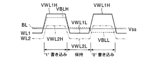
図35A及び図35Bは、データ書き込み時のワード線WL1,WL2及びビット線BLの電圧波形を示している。対をなす第1のワード線WL1と第2のワード線WL2は同期して駆動する。図35Aは、第1のゲート13と第2のゲート20とを別々に形成した場合に、第2のゲート20を第1のゲート13より低い電位で制御して、チャネルボディの第2のゲート20側に多数キャリア蓄積を可能とするものである。一方、図35Bは、第1のゲート13と第2のゲート20を同じ電位で駆動して、チャネルボディの第2のゲート20側に多数キャリア蓄積を可能とするものである。この図35Bの電圧波形は、第1のゲート13と第2のゲート20とを共通に形成した場合にも、同様に適用される。
【0101】
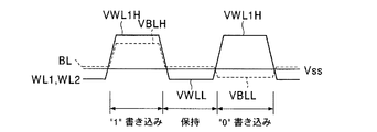
図35Aの場合、“1”データ書き込み時、選択された第1のワード線WL1に基準電位VSSより高い正の電位VWL1Hを与え、同時に選択された第2のワード線WL2にはそれより低い電位VWL2H(図の例では基準電位VSSより高い正電位)を与え、選択されたビット線BLには、基準電位VSSより高い正の電位VBLHを与える。これにより、選択されたメモリセルMCにおいて、5極管動作によるインパクトイオン化が生じ、ホールがチャネルボディに蓄積される。
【0102】
データ保持は、第1のワード線WL1に基準電位VSSより低い負の電位VWL1Lを与え、第2のワード線WL2にはそれより更に低い電位VWL2Lを与える。これにより、チャネルボディに過剰ホールを蓄積した状態である“1”データを保持する。
【0103】
“0”データ書き込み時は、選択された第1及び第2のワード線WL1及びWL2にそれぞれ“1”書き込み時と同様の電位VWL1H及びVWL2Hを与え、選択されたビット線BLには基準電位VSSより低い負の電位VBLLを与える。これにより、選択されたメモリセルMCにおいて、ドレイン接合が順バイアスになり、チャネルボディのホールがドレイン14に排出されて、チャネルボディ電位の低い状態である“0”データが書かれる。
【0104】
図35Bの場合、“1”データ書き込み時、選択された第1及び第2のワード線WL1及びWL2に基準電位VSSより高い正の電位VWLHを与え、選択ビット線BLには、基準電位VSSより高い正の電位VBLHを与える。これにより、選択されたメモリセルMCにおいて、5極管動作によるインパクトイオン化が生じ、ホールがチャネルボディに蓄積される。
【0105】
データ保持は、第1及び第2のワード線WL1及びWL2に基準電位VSSより低い負の電位VWLLを与える。これにより、チャネルボディに過剰ホールを蓄積した状態である“1”データを保持する。
【0106】
“0”データ書き込み時は、選択された第1及び第2のワード線WL1及びWL2に“1”書き込み時と同様の電位VWLHを与え、選択ビット線BLには基準電位VSSより低い負の電位VBLLを与える。これにより、選択されたメモリセルMCでドレイン接合が順バイアスになり、チャネルボディのホールがドレインに排出されて、チャネルボディ電位の低い状態である“0”データが書かれる。
【0107】
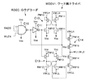
次に、この実施の形態におけるロウデコーダとワード線ドライバの具体的な回路構成の一例を説明する。図35Cは、ロウデコーダの一例と、図35Bに示したワード線WL1、WL2の電圧波形を生成するためのワード線ドライバWDDV1の一例を示す図である。
【0108】
この図35Cに示すように、ロウデコーダRDECは、NAND回路C10により構成されており、ワード線ドライバWDDV1は、インバータ回路C11と、レベル変換回路C12と、レベル変換回路C13と、出力バッファ回路C14とにより構成されている。この構成により、ロウデコーダRDECにより選択されたワード線ドライバWDDV1は、ハイレベルの電位を、正の電位VCCより高い電位であるVWLHに変換して、ワード線WL1、WL2に供給する。
【0109】
より具体的には、NAND回路C10には、ロウアドレス信号RADDとワード線イネーブル信号WLENとが、入力される。選択されたワード線WL1、WL2に対応するワード線ドライバWDDV1には、すべてハイレベルのロウアドレス信号RADDと、ハイレベルのワード線イネーブル信号WLENが入力される。したがって、選択されたワード線WL1、WL2に対応するワード線ドライバWDDV1のNAND回路C10の出力は、ローレベル、つまり基準電位VSSになる。NAND回路C10の出力は、インバータ回路C11に入力される。
【0110】
このインバータ回路C11は、入力された信号を反転して出力する。したがって、選択されたワード線ドライバWDDV1においては、インバータ回路C11の出力はハイレベル、つまり正の電位VCCになる。このインバータ回路C11の出力は、レベル変換回路C12とレベル変換回路C13とに入力される。また、レベル変換回路C12とレベル変換回路C13には、NAND回路C10の出力も、入力される。
【0111】
このレベル変換回路C12及びレベル変換回路C13の出力は、出力バッファ回路C14に入力される。レベル変換回路C12と出力バッファ回路C14とにより、インバータ回路C11のハイレベル出力電位であるVCCの出力を、VCCよりも高い正の電位であるVWLHに変換して、ワード線WL1、WL2に供給する。また、レベル変換回路C13と出力バッファ回路C14とにより、インバータ回路C11のローレベル出力電位であるVSSの出力を、VSSよりも低い電位であるVWLLに変換して、ワード線WL1、WL2に供給する。
【0112】
この実施の形態においては、レベル変換回路C12は、p型MOSトランジスタPM10、PM11と、n型MOSトランジスタNM10、NM11とを、備えて構成されている。p型MOSトランジスタPM10、PM11のソース端子は、それぞれ、電位VWLHの供給線に接続されており、そのドレイン端子は、それぞれ、n型MOSトランジスタNM10、NM11のドレイン端子に接続されている。また、p型MOSトランジスタPM10のゲート端子は、p型MOSトランジスタPM11とn型MOSトランジスタNM11の間のノードに接続されており、p型MOSトランジスタPM11のゲート端子は、p型MOSトランジスタPM10とn型MOSトランジスタNM10の間のノードに接続されている。
【0113】
n型MOSトランジスタNM10のゲート端子には、インバータ回路C11の出力が入力され、n型MOSトランジスタNM11のゲート端子には、NAND回路C10の出力が入力される。これらn型MOSトランジスタNM10、NM11のソース端子は、ぞれぞれ、電位VSSの供給線に接続されている。
【0114】
一方、レベル変換回路C13は、p型MOSトランジスタPM12、PM13と、n型MOSトランジスタNM12、NM13とを、備えて構成されている。p型MOSトランジスタPM12、PM13のソース端子は、それぞれ、電位VCCの供給線に接続されており、そのドレイン端子は、それぞれ、n型MOSトランジスタNM12、NM13のドレイン端子に接続されている。また、p型MOSトランジスタPM12のゲート端子には、インバータ回路C11の出力が入力され、p型MOSトランジスタPM13のゲート端子には、NAND回路C10の出力が入力される。
【0115】
n型MOSトランジスタNM12のゲート端子は、p型MOSトランジスタPM13とn型MOSトランジスタNM13との間のノードに接続されており、n型MOSトランジスタNM13のゲート端子は、p型MOSトランジスタPM12とn型MOSトランジスタNM12との間のノードに接続されている。また、これらn型MOSトランジスタNM12、NM13のソース端子は、ぞれぞれ、電位VWLLの供給線に接続されている。
【0116】
出力バッファ回路C14は、p型MOSトランジスタPM14、PM15と、n型MOSトランジスタNM14、NM15とを、直列的に接続することにより、構成されている。
【0117】
p型MOSトランジスタPM14のソース端子は、電位VWLHの供給線に接続されており、そのゲート端子は、レベル変換回路C12におけるp型MOSトランジスタPM11のゲート端子に接続されている。p型MOSトランジスタPM14のドレイン端子は、p型MOSトランジスタPM15のソース端子に接続されている。このp型MOSトランジスタPM15のゲート端子には、電位VSSが入力されている。このため、p型MOSトランジスタPM15は、ノーマリーオンのMOSトランジスタとなる。また、p型MOSトランジスタPM15のドレイン端子は、n型MOSトランジスタNM14のドレイン端子に接続されている。これらp型MOSトランジスタPM15とn型MOSトランジスタNM14との間のノードから、ワード線WL1、WL2を駆動するための電圧が出力される。
【0118】
n型MOSトランジスタNM14のゲート端子には、電位VCCが供給されている。このため、n型MOSトランジスタNM14は、ノーマリーオンのMOSトランジスタとなる。n型MOSトランジスタNM14のソース端子は、n型MOSトランジスタNM15のドレイン端子に接続されている。このn型MOSトランジスタNM15のゲート端子は、レベル変換回路C13におけるn型MOSトランジスタNM13のゲート端子に接続されている。また、n型MOSトランジスタNM15のソース端子は、電位VWLLの供給線に接続されている。
【0119】
以上のような構成のロウデコーダRDECとワード線ドライバWDDV1を用いて、図35Bに示す電位VWLH、VWLLを生成し、ワード線WL1、WL2に供給する。なお、図35Cにおいては、各MOSトランジスタでバックゲート接続がなされているが、これは必ずしも必要なものではない。
【0120】
なお、このワード線ドライバWDDV1の出力バッファ回路C14は、ノーマリーオンのMOSトランジスタPM15、NM14を備えているが、これは、MOSトランジスタPM14、NM15に、直接、電位VWLHと電位VWLLの電位差が印加しないようにするためである。すなわち、ノーマリーオンのMOSトランジスタPM15、NM14により、そのしきい値落ちをする分の電圧だけ、電位差が減少する。したがって、直接この電位差が、MOSトランジスタPM14、PM15に印加されてもよいのであれば、MOSトランジスタPM15、NM14は、図35Dに示すように、省略することも可能である。
【0121】
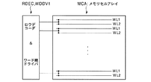
これら図35C又は図35Dに示したロウデコーダRDECとワード線ドライバWDDV1とを、メモリセルアレイMCAに配置したレイアウト図を、図35Eに示す。この図35Eに示すように、ワード線ドライバWDDV1のレイアウトピッチが、ワード線WL1、WL2の配線ピッチと一致する場合は、メモリセルアレイMCAの片側に、ロウデコーダRDECとワード線ドライバWDDV1とを配置することができる。
【0122】
これに対して、ワード線ドライバWDDV1のレイアウト面積が大きくなり、ワード線ドライバWDDV1のレイアウトピッチを、ワード線WL1、WL2の配線ピッチに一致させることができない場合、図35Fに示すようなレイアウトが考えられる。すなわち、メモリセルアレイMCAの両側にロウデコーダRDECとワード線ドライバWDDV1とを配置し、例えば、メモリセルアレイMCAの左側のロウデコーダRDECとワード線ドライバWDDV1で、奇数番目のワード線WL1、WL2のデコードと駆動を行い、メモリセルアレイMCAの右側のロウデコーダRDECとワード線ドライバWDDV1で、偶数番目のワード線WL1、WL2のデコードと駆動を行うようにする。
【0123】
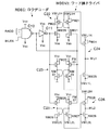
次に、図35Aに対応するロウデータとワード線ドライバの回路構成を説明する。図35Gは、ロウデコーダの一例と、図35Aに示したワード線WL1、WL2の電圧波形を生成するためのワード線ドライバWDDV2の一例を示す図である。
【0124】
この図35Gに示すように、ロウデコーダRDECは、NAND回路C10により構成されており、ワード線ドライバWDDV2は、インバータ回路C11と、レベル変換回路C22と、レベル変換回路C23と、出力バッファ回路C24と、レベル変換回路C25と、出力バッファ回路C26とにより構成されている。ここでの電圧の高低関係は、図35Aの例に従って、VWL1H>VWL2H>VSS>VWL1L>VWL2Lである。
【0125】
図35Cと異なる点のみ説明すると、レベル変換回路C22は基本的に図35Cのレベル変換回路C12と同様の構成であり、p型MOSトランジスタPM20、PM21と、n型MOSトランジスタNM20、NM21とを備えている。但し、p型MOSトランジスタPM20、PM21のソース端子は、電位VWL1Hの供給線に接続されている。
【0126】
レベル変換回路C23も、基本的に図35Cのレベル変換回路C13と同様の構成であり、p型MOSトランジスタPM22、PM23と、n型MOSトランジスタNM22、NM23とを備えている。但し、n型MOSトランジスタNM22、NM23のソース端子は、電位VWL1Lの供給線に接続されている。
【0127】
出力バッファ回路C24も、基本的に図35Cの出力バッファ回路C14と同様の構成であり、直列的に接続されたp型MOSトランジスタPM24、PM25と、n型MOSトランジスタNM24、NM25とを備えている。但し、p型MOSトランジスタPM24のソース端子は、電位VWL1Hの供給線に接続されており、n型MOSトランジスタNM25のソース端子は、電位VWL1Lの供給線に接続されている。
【0128】
これに加えて、図35Gのワード線ドライバWDDV2は、レベル変換回路C25と出力バッファ回路C26とを備えている。レベル変換回路C25の構成はレベル変換回路C23の構成と同様であり、p型MOSトランジスタPM26、PM27と、n型MOSトランジスタNM26、NM27とを備えている。但し、n型MOSトランジスタNM26、NM27のソース端子は、電位VWL2Lの供給線に接続されている。
【0129】
出力バッファ回路C26は、出力バッファ回路C24と同様の構成であるが、p型MOSトランジスタPM28とn型MOSトランジスタNM28の2つのMOSトランジスタにより構成されている。そして、p型MOSトランジスタPM28のソース端子は、電位VWL2Hの供給線に接続されており、n型MOSトランジスタNM28のソース端子は、電位VWL2Lの供給線に接続されている。
【0130】
ノーマリーオンのMOSトランジスタが挿入されていないのは、図35Aからも分かるように、電位VWL2Hと電位VWL2Lとの電位差はそれほど大きくないので、この電位差が直接MOSトランジスタPM28、NM28に印加されても、問題が生じないからである。
【0131】
この構成から分かるように、出力バッファ回路C24の出力は、電位VWL1Hと電位VWL1Lとの間で振幅し、これにより、第1のワード線WL1が駆動される。また、出力バッファ回路C26の出力は、電位VWL2Hと電位VWL2Lとの間で、出力バッファ回路C24の出力と同期して振幅し、これにより、第2のワード線WL2が駆動される。なお、図35Gにおいては、各MOSトランジスタでバックゲート接続がなされているが、これは必ずしも必要なものではない。
【0132】
また、図35Dに示したワード線ドライバWDDV1と同様に、図35Hに示すようにワード線ドライバWDDV2においても、p型MOSトランジスタPM25とn型MOSトランジスタNM24とを、省くことも可能である。
【0133】
これら図35G又は図35Hに示したロウデコーダRDECとワード線ドライバWDDV2とを、メモリセルアレイMCAに配置したレイアウト図を、図35Iに示す。図35G及び図35Hに示したワード線ドライバWDDV2においては、第1のワード線WL1と第2のワード線WL2を異なる電位で同期的に駆動する関係上、そのレイアウト面積が図35C及び図35Dに示したワード線ドライバWDDV1よりも大きくなってしまう。したがって、ワード線WL1、WL2の配線ピッチに、ワード線ドライバWDDV2のレイアウトピッチを一致させることは困難であると考えられる。このため、図35Iに示したレイアウトにおいては、メモリセルアレイMCAの両側に、ロウデコーダRDECとワード線ドライバWDDV2とを配置している。すなわち、メモリセルアレイMCAの左側のロウデコーダRDECとワード線ドライバWDDV2で、奇数番目のワード線WL1、WL2のデコードと駆動を行い、メモリセルアレイMCAの右側のロウデコーダRDECとワード線ドライバWDDV2で、偶数番目のワード線WL1、WL2のデコードと駆動を行う。
【0134】
また、図35Jに示すように、例えば、第1のワード線WL1用のワード線ドライバWDDV3を、メモリセルアレイMCAの左側に配置し、第2のワード線WL2のワード線ドライバWDDV4を、メモリセルアレイMCAの右側に配置するようにしてもよい。このように配置することにより、電源配線の引き回しを楽にすることができる。すなわち、第1のワード線WL1用のワード線ドライバWDDV3のあるメモリセルアレイMCAの左側にのみ、電位VWL1Hと電位VWL1Lの電位供給線を配線し、第2のワード線WL2用のワード線ドライバWDDV4のあるメモリセルアレイMCAの右側にのみ、電位VWL2Hと電位VWL2Lの電位供給線を配線すればよい。
【0135】
但し、このレイアウトの場合、ワード線ドライバWDDV3とワード線ドライバWDDV4の双方に、個別にロウデコーダRDECが必要になる。そのようなワード線ドライバWDDV3の例を図35Kに示し、ワード線ドライバWDDV4の例を図35Lに示す。
【0136】
図35Kに示すように、第1のワード線WL1用のワード線ドライバWDDV3は、インバータ回路C11を介してロウデコーダRDECに接続されたレベル変換回路C22と、直接ロウデコーダRDECに接続されたレベル変換回路C23と、出力バッファ回路C24とを備えている。これらの構成は上述した図35Gのワード線ドライバWDDV2と同様である。
【0137】
一方、図35Lに示すように、第2のワード線WL2用のワード線ドライバWDDV4は、ロウデコーダRDECと、インバータ回路C11と、レベル変換回路C25と、出力バッファ回路C26とを備えて構成されている。レベル変換回路C25と出力バッファ回路C26の構成は、上述した図35Gのワード線ドライバWDDV2と同様である。但し、ワード線ドライバWDDV4はメモリセルアレイMCAの右側に設けられているため、ロウデコーダRDECをワード線ドライバWDDV3と共用することができないため、独自にロウデコーダRDECとインバータ回路C11とを設けている。
【0138】
ワード線ドライバWDDV3のロウデコーダRDECと、WDD4のロウデコーダRDECとには、ロウアドレス信号RADDとWLENとが同期して入力されるので、結果的に、異なる電圧振幅で同期したワード線駆動電位が出力される。
【0139】
なお、図35K及び図35Lにおいては、各MOSトランジスタでバックゲート接続がなされているが、これは必ずしも必要なものではない。また、図35Kに示したワード線ドライバWDDV3においても、図35Mに示すように、p型MOSトランジスタPM25とn型MOSトランジスタNM24とを、省くことも可能である。
【0140】
【発明の効果】
以上述べたようにこの発明によれば、一つのメモリセルは、フローティングの半導体層を持つ単純な一つのトランジスタにより形成され、セルサイズを4F2と小さくすることができる。トランジスタのソースは固定電位に接続され、ドレインに接続されたビット線とゲートに接続されたワード線の制御のみによって、読み出し,書き換え及びリフレッシュの制御が行われる。トランジスタのチャネルボディに対向する第2のゲートを設け、この第2のゲートが対向する表面部には高濃度層を設けることにより、第2のゲートをチャネルボディに容量結合させることによって、“0”,“1”データのしきい値電圧差を大きくすることができる。
【図面の簡単な説明】
【図1】この発明の基本コンセプトによるメモリセルの基本構造を示す断面図である。
【図2】同メモリセルの等価回路である。
【図3】同メモリセルを用いてDRAMのメモリセルアレイを構成した場合のレイアウトである。
【図4A】図3のA−A’断面図である。
【図4B】図3のB−B’断面図である。
【図5】同メモリセルのワード線電位とチャネルボディ電位の関係を示す図である。
【図6】同メモリセルの読み出し方式を説明するための図である。
【図7】同メモリセルの他の読み出し方式を説明するための図である。
【図8】同DRAMの“1”データ読み出し/リフレッシュの動作波形を示す図である。
【図9】同DRAMの“0”データ読み出し/リフレッシュの動作波形を示す図である。
【図10】同DRAMの“1”データ読み出し/“0”データ書き込みの動作波形を示す図である。
【図11】同DRAMの“0”データ読み出し/“1”データ書き込みの動作波形を示す図である。
【図12】同DRAMの他の読み出し方式による“1”データ読み出し/リフレッシュの動作波形を示す図である。
【図13】同DRAMの他の読み出し方式による“0”データ読み出し/リフレッシュの動作波形を示す図である。
【図14】同DRAMの他の読み出し方式による“1”データ読み出し/“0”データ書き込みの動作波形を示す図である。
【図15】同DRAMの他の読み出し方式による“0”データ読み出し/“1”データ書き込みの動作波形を示す図である。
【図16】同メモリセルの“0”書き込み/読み出しのシミュレーションによるチャネルボディ電位変化を示す図である。
【図17】同メモリセルの“1”書き込み/読み出しのシミュレーションによるチャネルボディ電位変化を示す図である。
【図18】同シミュレーションによる“0”,“1”データの読み出し時のドレイン電流−ゲート電圧特性を示す図である。
【図19A】この発明の実施の形態1によるメモリセルの構造を示す断面図である。
【図19B】図19Aに示すメモリセルをマトリクス配列したメモリセルアレイの等価回路を示す図である。
【図19C】図19Aに示すメモリセルをマトリクス配列したメモリセルアレイのレイアウトを示す図である。
【図19D】図19CのA−A’断面図である。
【図19E】図19CのB−B’断面図である。
【図19F】実施の形態1によるメモリセルの変形例を示す斜視図である。
【図19G】図19FのメモリセルのA−A’断面図である。
【図19H】図19FのメモリセルのB−B’断面図である。
【図19I】図19Fに示すメモリセルをマトリクス配列したメモリセルアレイのレイアウトを示す図である。
【図19J】図19IのA−A’断面図である。
【図19K】図19IのB−B’断面図である。
【図19L】図19IのC−C’断面図である。
【図19M】実施の形態1によるメモリセルの別の変形例を示す斜視図である。
【図19N】図19MのメモリセルのB−B’断面図である。
【図20】実施の形態2によるメモリセルの構造を示す断面図である。
【図21】実施の形態3によるメモリセルアレイの平面図である。
【図22】図21のA−A’断面図である。
【図23】実施の形態4によるメモリセルアレイの平面図である。
【図24】図23のA−A’断面図である。
【図25A】実施の形態5によるメモリセルの構造を示す断面図である。
【図25B】図25Aに示すメモリセルにおいて、ドレイン領域に正の電位を印加し、ゲートに正の電位を印加し、ソース領域をグランドに接続した場合における、メモリセルの状態を示す模式図である。
【図25C】図25Aに示すメモリセルにおいて、ドレイン領域に負の電位を印加し、ゲートに正の電位を印加し、ソース領域をグランドに接続した場合における、メモリセルの状態を示す模式図である。
【図26】同実施の形態のメモリセルの特性を示す図である。
【図27】実施の形態6によるメモリセルの構造を示す断面図である。
【図28】実施の形態6によるメモリセルの別の構造を示す断面図である。
【図29A】SGT構造のメモリセルにゲートオフセット構造を適用した場合のメモリセルアレイの平面図である(実施の形態6)。
【図29B】図29AによるメモリセルアレイのA−A’断面図である。
【図30A】実施の形態3において、ゲートオフセット構造を導入した場合のメモリセルアレイの平面図である(実施の形態6)。
【図30B】図30AによるメモリセルアレイのA−A’断面図である。
【図30C】実施の形態4において、ゲートオフセット構造を導入した場合のメモリセルアレイの平面図である(実施の形態6)。
【図30D】図30CによるメモリセルアレイのA−A’断面図である。
【図31】MISFETのGIDL電流を示す特性図である(実施の形態7)。
【図32】GIDL電流を用いた“1”書き込み/読み出しの動作波形図である。
【図33】実施の形態8によるメモリセルアレイの平面図である。
【図34A】図33のA−A’断面図である。
【図34B】図33のB−B’断面図である。
【図35A】第1のゲートと第2のゲートとを異なる電位で同期駆動した場合における、メモリセルの書き込み動作を示す波形図である(実施の形態9)。
【図35B】第1のゲートと第2のゲートとを同電位で駆動した場合における、メモリセルの書き込み動作を示す波形図である(実施の形態9)。
【図35C】図35Bの書き込み動作波形を生成するためのワード線ドライバとロウデコーダの回路構成の一例を示す図である。
【図35D】図35Cに示したワード線ドライバの変形例を示す図である。
【図35E】図35C又は図35Dに示したロウデコーダとワード線ドライバとを、メモリセルアレイに対して配置した場合のレイアウトの一例を示す図である(片側配置)。
【図35F】図35C又は図35Dに示したロウデコーダとワード線ドライバとを、メモリセルアレイに対して配置した場合のレイアウトの一例を示す図である(両側配置)。
【図35G】図35Aの書き込み動作波形を生成するためのワード線ドライバとロウデコーダの回路構成の一例を示す図である。
【図35H】図35Gに示したワード線ドライバの変形例を示す図である。
【図35I】図35G又は図35Hに示したロウデコーダとワード線ドライバとを、メモリセルアレイに対して配置した場合のレイアウトの一例を示す図である(第1のワード線と第2のワード線とからなる対のワード線に対して、左右交互にロウデコーダとワード線ドライバとを設けた場合)。
【図35J】図35G又は図35Hに示したロウデコーダとワード線ドライバとを、メモリセルアレイに対して配置した場合のレイアウトの一例を示す図である(片側に第1のワード線用のロウデコーダとワード線ドライバとを設け、もう片側に第2のワード線のロウデコーダとワード線ドライバとを設けた場合)。
【図35K】図35Jに示したレイアウトを採用する場合における、第1のワード線用のロウデコーダとワード線ドライバの回路構成の一例を示す図である。
【図35L】図35Jに示したレイアウトを採用する場合における、第2のワード線用のロウデコーダとワード線ドライバの回路構成の一例を示す図である。
【図35M】図35Kに示したワード線ドライバの変形例を示す図である。
【符号の説明】
10 シリコン基板
11 シリコン酸化膜
12 p型シリコン層
13 第1のゲート
14 ドレイン拡散層
15 ソース拡散層
20 第2のゲート[0001]
BACKGROUND OF THE INVENTION
The present invention relates to a semiconductor memory device that dynamically stores data using a channel body of a transistor as a storage node.
[0002]
[Prior art]
In a conventional DRAM, a memory cell is composed of a MOS transistor and a capacitor. The miniaturization of DRAM is greatly advanced by adopting a trench capacitor structure or a stacked capacitor structure. Currently, the unit memory cell size (cell size) is 2F × 4F = 8F, where F is the minimum processing dimension. 2 It has been reduced to the area of. That is, the minimum processing dimension F becomes smaller with the generation, and the cell size is generally set to αF. 2 , The coefficient α becomes smaller with the generation, and α = 8 is realized at present when F = 0.18 μm.
[0003]
[Problems to be solved by the invention]
In order to secure the same cell size or chip size trend as before, it is required to satisfy α <8 when F <0.18 μm, and α <6 when F <0.13 μm. How to form a cell size in a small area along with processing becomes a big problem. Therefore, the memory cell of 1 transistor / 1 capacitor is 6F 2 And 4F 2 Various proposals have been made to make the size of. However, there are technical difficulties such as having to make the transistor vertical, problems such as increased electrical interference between adjacent memory cells, and difficulties in manufacturing technology such as processing and film generation, and practical application is not easy. Absent.
[0004]
SUMMARY OF THE INVENTION Accordingly, an object of the present invention is to provide a semiconductor memory device capable of dynamically storing data using a memory cell having a simple transistor structure.
[0005]
[Means for Solving the Problems]
A semiconductor memory device according to the present invention is a semiconductor memory device having a plurality of MIS transistors for constituting a memory cell, and each MIS transistor includes:
A semiconductor layer;
A source region formed in the semiconductor layer;
A drain region formed apart from the source region in the semiconductor layer, wherein the semiconductor layer between the source region and the drain region becomes a channel body in a floating state; and
A first gate for forming a channel in the channel body;
A second gate for controlling the potential of the channel body by capacitive coupling;
A high concentration region formed on the second gate side of the channel body, the high concentration region having the same conductivity type as the channel body and having an impurity concentration higher than the impurity concentration of the channel body;
With
The MIS transistor dynamically stores a first data state in which the channel body is set to a first potential and a second data state in which the channel body is set to a second potential.
It is characterized by that.
[0006]
Further, a semiconductor memory device according to the present invention is a semiconductor memory device having a plurality of MIS transistors for constituting a memory cell, and each MIS transistor includes:
A semiconductor layer;
A source region formed in the semiconductor layer;
A drain region formed apart from the source region in the semiconductor layer, wherein the semiconductor layer between the source region and the drain region becomes a channel body in a floating state; and
A first gate for forming a channel in the channel body;
With
The first gate is disposed so that the amount of overlap with the source region is positive and the amount of overlap with the drain region is negative, and the first gate is offset with respect to the drain region. ,
A drain region of the MIS transistor is connected to a bit line; a first gate of the MIS transistor is connected to a first word line; and a source region of the MIS transistor is connected to a source line;
The source region and the drain region are composed of an n-type semiconductor layer, and the channel body between the source region and the drain region is composed of a p-type semiconductor layer,
With the source line potential fixed at 0V, the first word line is set to a positive potential and the bit line is set to a positive potential, thereby writing the first data state to the MIS transistor; The apparatus further comprises writing means for writing the second data state to the MIS transistor by setting the first word line to a positive potential and the bit line to a negative potential.
[0007]
A semiconductor memory device according to the present invention is a semiconductor memory device having a plurality of MIS transistors for constituting a memory cell, and each MIS transistor includes:
A semiconductor layer;
A source region formed in the semiconductor layer;
A drain region formed apart from the source region in the semiconductor layer, wherein the semiconductor layer between the source region and the drain region becomes a channel body in a floating state; and
A gate for forming a channel in the channel body;
With
A drain region of the MIS transistor is connected to a bit line, a gate of the MIS transistor is connected to a word line, and a source region of the MIS transistor is connected to a source line;
The source region and the drain region are composed of an n-type semiconductor layer, and the channel body between the source region and the drain region is composed of a p-type semiconductor layer,
The first data state is written to the MIS transistor by setting the word line to a negative potential and the bit line to a positive potential in a state where the potential of the source line is fixed at 0V, and the word line A writing means for writing the second data state to the MIS transistor by setting the bit line to a negative potential and the bit line to a negative potential;
It is characterized by that.
[0008]
DETAILED DESCRIPTION OF THE INVENTION
Embodiments of the present invention will be described below with reference to the drawings.
[0009]
[Basic concept]
FIG. 1 shows a basic sectional structure of a unit memory cell MC of a DRAM according to each embodiment described later, and FIG. 2 shows an equivalent circuit thereof. The memory cell MC is composed of an N-channel MIS transistor having an SOI structure. That is, an SOI substrate in which a
[0010]
The sources and drains 14 and 15 are formed to a depth reaching the bottom
[0011]
When the memory cells MC are arranged in a matrix, the
[0012]
FIG. 3 shows a layout of the memory cell array, and FIGS. 4A and 4B show AA ′ and BB ′ cross sections of FIG. 3, respectively. The p-
[0013]
The transistor is covered with an
[0014]
As a result, the
[0015]
In this memory cell array configuration, assuming that the word lines WL and the bit lines BL are formed at a pitch of the minimum processing dimension F, the unit cell area is 2F × 2F = 4F as shown by the broken line in FIG. 2 It becomes.
[0016]
The operation principle of the memory cell MC composed of the n-channel type MIS transistor utilizes accumulation of holes which are majority carriers in the channel body of the MIS transistor (p-
[0017]
Data “0” and “1” are stored as a difference in channel body potential, and thus as a threshold voltage difference between transistors. That is, the threshold voltage Vth1 in the data “1” state in which the potential of the channel body is high due to hole accumulation is lower than the threshold voltage Vth0 in the data “0” state. In order to maintain the “1” data state in which holes, which are majority carriers, are stored in the body, it is necessary to apply a negative bias voltage to the word line. In theory, this data holding state does not change even if the read operation is performed as long as the read operation is performed in the linear region and the reverse data write operation (erase) is not performed. That is, unlike a one-transistor / one-capacitor DRAM that uses capacitor charge storage, non-destructive readout is possible.
[0018]
There are several possible methods for reading data. The relationship between the word line potential Vwl and the channel body potential VB is as shown in FIG. 5 in relation to the data “0” and “1”. Therefore, in the first method of reading data, a read potential that is intermediate between the threshold voltages Vth0 and Vth1 of the data “0” and “1” is applied to the word line WL, and current flows in the memory cell of “0” data. The fact that the current flows in the memory cell of “1” data is used. Specifically, for example, the bit line BL is precharged to a predetermined potential VBL, and then the word line WL is driven. Thereby, as shown in FIG. 6, in the case of “0” data, there is no change in the bit line precharge potential VBL, and in the case of “1” data, the precharge potential VBL decreases.
[0019]
The second read method utilizes the fact that the rising speed of the bit line potential varies depending on the conductivity of “0” and “1” by supplying current to the bit line BL after the word line WL is raised. To do. Briefly, the bit line BL is precharged to 0V, the word line WL is raised as shown in FIG. 7, and a bit line current is supplied. At this time, it is possible to discriminate data by detecting the difference in potential rise of the bit line using the dummy cell.
[0020]
The third reading method is a method of reading a difference between bit line currents different between “0” and “1” when the bit line BL is clamped to a predetermined potential. In order to read out the current difference, a current-voltage conversion circuit is required. Finally, the potential difference is differentially amplified to output a sense output.
[0021]
In the present invention, in order to selectively write "0" data, that is, holes are emitted only from the channel body of the memory cell selected by the potential of the word line WL and bit line BL selected in the memory cell array. In this case, capacitive coupling between the word line WL and the channel body becomes essential. When holes are accumulated in the channel body with data “1”, the word line is sufficiently biased in the negative direction, and the gate-channel body capacitance of the memory cell becomes the gate oxide film capacitance (that is, the surface is depleted). It is necessary to hold in a state in which no layer is formed.
[0022]
In the write operation, both “0” and “1” preferably reduce power consumption as pulse write. When “0” is written, a hole current flows from the channel body to the drain of the selection transistor and an electron current flows from the drain to the channel body, but holes are not injected into the channel body.
[0023]
More specific operation waveforms will be described. 8 to 11 show operation waveforms of read / refresh and read / write in the case of using the first read method in which data is discriminated based on the presence / absence of discharge of the bit line by the selected cell.
[0024]
8 and 9 show read / refresh operations of “1” data and “0” data, respectively. Until time t1, the data is held (non-selected state), and a negative potential is applied to the word line WL. At time t1, the word line WL is raised to a predetermined positive potential. At this time, the word line potential is set between the threshold values Vth0 and Vth1 of “0” and “1” data. As a result, in the case of “1” data, the bit line VBL precharged in advance becomes a low potential by discharging. In the case of “0” data, the bit line potential VBL is held. Thereby, “1” and “0” data are discriminated.
[0025]
At time t2, the potential of the word line WL is further increased. At the same time, when the read data is “1”, a positive potential is applied to the bit line BL (FIG. 8), and when the read data is “0”. A negative potential is applied to the bit line BL (FIG. 9). As a result, when the selected memory cell is “1” data, a large channel current flows due to the pentode operation, impact ionization occurs, excessive holes are injected and held in the channel body, and “1” data is written again. In the case of “0” data, the drain junction becomes a forward bias, and “0” data in which excess holes are not held in the channel body is written again.
[0026]
At time t3, the word line WL is biased in the negative direction, and the read / refresh operation is terminated. In other unselected memory cells connected to the same bit line BL as the memory cell from which “1” data is read, the word line WL is held at a negative potential, and therefore the channel body is held at a negative potential, and impact ionization does not occur. In other unselected memory cells connected to the same bit line BL as the memory cell from which “0” data is read, the word line WL is also held at a negative potential, and no hole emission occurs.
[0027]
10 and 11 show read / write operations of “1” data and “0” data, respectively, by the same read method. The read operation at time t1 in FIGS. 10 and 11 is the same as that in FIGS. 8 and 9, respectively. After reading, when the word line WL is set to a higher potential at time t2 and “0” data is written to the same selected cell, a negative potential is simultaneously applied to the bit line BL (FIG. 10) and “1” data is written. A positive potential is applied to the bit line BL (FIG. 11). As a result, in the cell to which “0” data is given, the drain junction becomes a forward bias, and the channel body hole is emitted. In a cell to which “1” data is given, impact ionization occurs near the drain, and excess holes are injected and held in the channel body.
[0028]
12 to 15 use the second reading method in which the bit line BL is precharged to 0 V, a current is supplied to the bit line BL after the word line is selected, and data is discriminated based on the potential rise speed of the bit line BL. The read / refresh and read / write operation waveforms are shown.
[0029]
12 and 13 show read / refresh operations of “1” data and “0” data, respectively. The word line WL held at the negative potential is raised to the positive potential at time t1. At this time, as shown in FIG. 7, the word line potential is set to a value higher than the threshold values Vth0 and Vth1 of “0” and “1” data. Alternatively, the word line potential may be set between the threshold values Vth0 and Vth1 of “0” and “1” data, as in the first reading method. Then, current is supplied to the bit line at time t2. Thereby, in the case of “1” data, the memory cell is turned on deeply and the potential rise of the bit line BL is small (FIG. 12). In the case of “0” data, the current of the memory cell is small (or no current flows). The bit line potential rises rapidly. Thereby, “1” and “0” data are discriminated.
[0030]
At time t3, when the read data is “1”, a positive potential is applied to the bit line BL (FIG. 12), and when the read data is “0”, a negative potential is applied to the bit line BL (FIG. 12). FIG. 13). As a result, when the selected memory cell is “1” data, drain current flows, impact ionization occurs, excess holes are injected and held in the channel body, and “1” data is written again. In the case of “0” data, the drain junction becomes a forward bias, and “0” data without excess holes in the channel body is written again.
[0031]
At time t4, the word line WL is biased in the negative direction, and the read / refresh operation is terminated.
[0032]
14 and 15 show read / write operations of “1” data and “0” data, respectively, by the same read method. Read operations at times t1 and t2 in FIGS. 14 and 15 are the same as those in FIGS. 12 and 13, respectively. After reading, when writing “0” data to the same selected cell, a negative potential is applied to the bit line BL (FIG. 14), and when writing “1” data, a positive potential is applied to the bit line BL (FIG. 15). ). As a result, in the cell to which “0” data is given, the drain junction becomes a forward bias, and excess holes in the channel body are discharged. In a cell to which “1” data is given, a large drain current flows, impact ionization occurs near the drain, and excess holes are injected and held in the channel body.
[0033]
As described above, the memory cell MC according to the present invention is configured by a simple MIS transistor having a floating channel body electrically isolated from other elements. 2 Cell sizes can be achieved. Further, the potential control of the floating channel body uses capacitive coupling from the gate electrode, and the source is also at a fixed potential. That is, the read / write control is performed by the word line WL and the bit line BL and is simple. Further, since the memory cell MC is basically non-destructive reading, it is not necessary to provide a sense amplifier for each bit line, and the layout of the sense amplifier becomes easy. Furthermore, since it is a current reading method, it is resistant to noise, and for example, reading is possible even with an open bit line method. Also, the manufacturing process of the memory cell is simple.
[0034]
The SOI structure is an important technology when considering future performance improvement of logic LSIs. The DRAM according to the present invention is very promising when it is mixed with a logic LSI having such an SOI structure. This is because, unlike a conventional DRAM using a capacitor, a process different from that of a logic LSI is not required, and the manufacturing process is simplified.
[0035]
Furthermore, the SOI structure DRAM according to the present invention has an advantage that superior memory retention characteristics can be obtained as compared with a conventional one-transistor / one-capacitor DRAM having an SOI structure. That is, when the conventional one-transistor / one-capacitor DRAM has an SOI structure, holes are accumulated in the floating channel body, the threshold value of the transistor is lowered, and the subthreshold current of the transistor is increased. This degrades the memory retention characteristics. On the other hand, in the memory cell having only one transistor according to the present invention, there is no transistor path for reducing the stored charge, the data retention characteristic is determined solely by the leakage of the pn junction, and the problem of subthreshold leakage is eliminated.
[0036]
In the basic memory cell described so far, how large the threshold voltage difference between data “0” and “1” stored as the channel body potential difference is important for the memory characteristics. According to the result of simulation regarding this point, when data is written with potential control of the channel body by capacitive coupling from the gate, the subsequent data is compared with the channel body potential difference between “0” and “1” data immediately after the writing. It has been clarified that the channel body potential difference between “0” and “1” data in the holding state becomes small. The simulation result will be described next.
[0037]
The device conditions are as follows: gate length Lg = 0.35 μm, p-
[0038]
FIG. 16 shows the gate potential Vg, the drain potential Vd, and the channel body potential VB in the “0” data write and the subsequent data retention and data read (respectively shown instantaneously). FIG. 17 similarly shows the gate voltage Vg, the drain voltage Vd, and the channel body voltage VB in “1” data writing, and subsequent data holding and data reading (respectively shown instantaneously).
[0039]
Further, in order to see the threshold voltage Vth0 of the “0” data and the threshold voltage Vth1 of the “1” data in the data read operation at the time t6-t7, the drain current Ids and the gate-source voltage Vgs at that time. Is drawn as shown in FIG. However, the channel width W and the channel length L are W / L = 0.175 μm / 0.35 μm, and the drain-source voltage is Vds = 0.2V.
[0040]
From FIG. 18, the difference ΔVth between the threshold voltage Vth0 of the “0” write cell and the threshold voltage Vth1 of the “1” write cell is ΔVth = 0.32V. From the above analysis results, the problem is that in FIG. 16 and FIG. 17, the channel body potential immediately after writing “0” (time t3) is VB = −0.77 V, and the channel body potential immediately after writing “1”. While VB = 0.85V and the difference is 1.62V, in the data holding state (time t6), the channel body potential of the “0” write cell is VB = −2.04V, “1” write The body potential of the cell is VB = −1.6 V, and the difference is 0.44 V, which is smaller than that immediately after writing.
[0041]
There are two possible causes for the difference between the channel body potential data in the subsequent data holding state as compared to immediately after writing.
[0042]
One is that the capacitive coupling from the gate to the channel body varies with the data. Immediately after writing "0" (t3-t4), the drain is -1.5V, but immediately after writing "1", the drain is 2V. Therefore, when the gate potential Vg is subsequently lowered, the channel is easily lost in the “1” write cell, the capacitance between the gate and the channel body becomes obvious, and holes are gradually accumulated in the channel body, thereby increasing the capacitance. On the other hand, in the “0” write cell, the channel does not disappear easily, and the gate-channel body capacitance does not become apparent.
[0043]
If the drain potential is reset to 200 mV before starting to lower the gate potential, it seems that the above-mentioned imbalance is eliminated. However, in this case, in the cell in which “0” is written, the drain potential rises in a state where the channel is formed, and a current due to the triode operation flows. Then, the channel body potential lowered by writing “0” is increased due to capacitive coupling between the n-type drain and channel inversion layer and the p-type channel body, which is not preferable.
[0044]
The other is that the channel body potential is influenced by the capacitance of the pn junction between the source or drain and the channel body between times t4 and t5 after writing, and this is the signal amount of “0” and “1” data. It is to act in the direction to reduce the.
[0045]
Therefore, a gate (second gate) for controlling the potential of the channel body by capacitive coupling is added to the basic memory cell in addition to a gate (first gate) for controlling channel formation. . In order to ensure the capacitance between the second gate and the channel body, the accumulation state (accumulation state) is maintained without forming the channel inversion layer on the surface on the second gate side. A high concentration region having the same conductivity type as the channel body is formed. The second gate is driven in synchronization with the first gate, for example, at a lower potential than the first gate or at the same potential. Alternatively, the second gate may be fixed at, for example, a reference potential applied to the source or a lower potential (a negative potential in the case of the n channel).
[0046]
Specific embodiments will be described below.
[0047]
[Embodiment 1]
FIG. 19A shows the structure of memory cell MC according to the first embodiment of the present invention, corresponding to FIG. The basic structure is the same as that of FIG. 1. The difference from FIG. 1 is that, apart from the
[0048]
In the memory cell MC of this embodiment, the
[0049]
In an actual memory cell array configuration, a plurality of memory cells MC shown in FIG. 19A are arranged in a matrix, the
[0050]
FIG. 19B shows an equivalent circuit of a memory cell array in which a plurality of such memory cells MC are arranged in a matrix. The first gate (G1) 13 of the plurality of memory cells MC arranged in one direction is connected to the first word line WL1, and the second gate (G2) 20 is connected to the second word line WL2. . A bit line BL to which the drain of the memory cell MC is connected is arranged in a direction crossing these word lines WL1 and WL2. The
[0051]
19C shows a layout of the memory cell array, and FIGS. 19D and 19E show cross sections taken along the lines AA ′ and BB ′ of FIG. 19C, respectively. The p-
[0052]
As a result, the
[0053]
In this memory cell array configuration, assuming that the word lines WL1 and WL2 and the bit lines BL are formed with a pitch of the minimum processing dimension F, the unit cell area is 2F × 2F = 4F as shown by the broken line in FIG. 19C. 2 It becomes.
[0054]
In such a configuration, the same operation as described above using the basic memory cell is performed. At this time, the second word line WL2 is driven at a lower potential than the first word line WL1 in synchronization with the first word line WL1. In this manner, by driving the
[0055]
That is, in the case of writing “0” data, a positive potential is applied to the
[0056]
However, in this embodiment, the potential of the channel body can be sufficiently increased by applying a positive potential also to the
[0057]
Further, data retention is performed by lowering the potential of the unselected first word line WL1, but at this time, the potential of the second word line WL2 making a pair is also lowered to control the channel body potential to be the same. When “0” data is written in another cell connected to the bit line, data destruction in an unselected cell holding “1” data is reliably prevented. Further, in the non-selected “0” data cell connected to the “1” write bit line, there is a concern of data breakdown due to surface breakdown or GIDL current. In this embodiment, the second word line Lowering the channel body potential also eliminates these concerns.
[0058]
Further, when the potential of the bit line is greatly lowered at the time of writing “0”, a current flows from the source to the bit line. In this embodiment, since the channel body potential is increased by the
[0059]
Also, when reading data, it is necessary to perform a triode operation so as not to erroneously write “1”. Therefore, although the bit line potential is lower than that at the time of writing “1”, the depletion layer extension between the drain and the channel body is smaller than that at the time of writing “1”, so that the capacitive coupling between the bit line and the channel body is increased. . This causes the carrier injected into the channel body at the time of writing to be redistributed, causing a drop in the channel body potential. In this embodiment, the majority carrier accumulation state of the channel body can be satisfactorily maintained by the control by the
[0060]
In the above description, the
[0061]
Further, the
[0062]
Further, in this embodiment, the
[0063]
FIG. 19F is a perspective view showing the configuration of the memory cell MC in which the
[0064]
As can be seen from these drawings, in this example, the
[0065]
p + The
[0066]
FIG. 19I is a diagram showing a layout of a memory cell array in which the memory cells MC shown in FIG. 19F are arranged in a matrix, and corresponds to FIG. 19C. 19J is a view showing a cross section taken along line AA ′ of FIG. 19I, FIG. 19K is a view showing a cross section taken along line BB ′ of FIG. 19I, and FIG. 19L is a cross section taken along line CC ′ of FIG. FIG.
[0067]
As can be seen from these figures, the
[0068]
In this memory cell MC, as shown in FIG. + The
[0069]
Such an example is shown in FIGS. 19M and 19N. FIG. 19M is a perspective view showing the configuration of the memory cell MC, and corresponds to FIG. 19F. 19N is a diagram showing a BB ′ cross section in FIG. 19M and corresponds to FIG. 19H. The cross section AA ′ in FIG. 19M is the same as FIG. 19G described above.
[0070]
As shown in FIGS. 19M and 19N, p + The
[0071]
On the other hand, as shown in FIGS. 19M and 19N, p + Such a situation can be avoided by forming the
[0072]
[Embodiment 2]
FIG. 20 shows the structure of the memory cell MC according to the second embodiment. Unlike the embodiment of FIG. 19A, in this embodiment, the
[0073]
As such a configuration, the
[0074]
[Embodiment 3]
FIG. 21 shows the layout of the memory cell array according to the third embodiment, and FIG. 22 shows the AA ′ cross section. In the embodiments described so far, an SOI substrate is used to make a transistor having a floating channel body. In this embodiment, a floating channel transistor (SGT) structure is used to form a floating channel. A memory cell is constituted by a vertical MIS transistor having a body.
[0075]
In the
[0076]
An n-type
[0077]
Also in this embodiment, the same operation as in the previous embodiments can be performed. According to this embodiment, it is not necessary to use an SOI substrate. Therefore, only a memory cell has a floating channel body made of a vertical transistor, and peripheral circuits such as a sense amplifier, a transfer gate, and a row / column decoder other than the cell array are provided. A normal planar transistor can be used. Therefore, unlike the case where an SOI substrate is used, it is not necessary to form a contact for fixing the channel body potential of the peripheral circuit transistor in order to eliminate the instability of the circuit due to the channel body floating effect. The area of the part can be reduced.
[0078]
[Embodiment 4]
FIG. 23 and FIG. 24 show the layout of the cell array of the embodiment using the same SGT structure as that of the third embodiment and its AA ′ cross section corresponding to FIG. 21 and FIG. The difference from the third embodiment is that the
[0079]
In the case of this embodiment, the
[0080]
[Embodiment 5]
FIG. 25A shows the structure of the memory cell MC of the embodiment that can improve the reliability of writing “0” data in correspondence with FIG. The memory cell structure of this embodiment is different from that of FIG. 1 in that the
[0081]
As shown in FIG. 25A, this can be easily realized by making the ion implantation of the
[0082]
In the memory cell in the above-described embodiment, “0” writing applies a forward bias between the
[0083]
On the other hand, as shown in FIG. 25A, when an offset structure is provided on the drain side, a normal potential is applied to the
[0084]
However, when a negative potential is applied to the
[0085]
Therefore, according to this embodiment, when “0” is written (that is, when a forward bias is applied between the
[0086]
In the above, the case where almost no current flows in the reverse direction has been described, but by providing a light asymmetry with a difference of 10% or more in the channel current, the effect of reducing the current can be obtained in the same manner. Further, providing the
[0087]
[Embodiment 6]
FIGS. 27 and 28 show embodiments in which a gate offset structure is similarly introduced for the memory cells MC of FIGS. 19A and 20, respectively. Similarly in this embodiment, useless current at the time of writing “0” can be reduced.
[0088]
29A and 29B show an embodiment in which a gate offset structure is similarly introduced to a memory cell MC using an SGT structure. FIG. 29A is a plan view showing a layout of a memory cell array composed of such memory cells MC, and FIG. 29B is a diagram showing a cross section taken along line AA ′ of FIG. 29A. As shown in FIGS. 29A and 29B, the
[0089]
As shown in FIG. 29B, a
[0090]
FIG. 30A is a plan view showing a layout of a memory cell array composed of memory cells into which a gate offset structure is introduced in the third embodiment of FIGS. 21 and 22. FIG. FIG. 30B is a diagram showing a cross section taken along line AA ′ in FIG. 30A. As shown in FIGS. 30A and 30B, the
[0091]
FIG. 30C is a plan view showing a layout of a memory cell array including memory cells into which a gate offset structure is introduced in the fourth embodiment shown in FIGS. FIG. 30D is a diagram showing an AA ′ cross section in FIG. 30C. As shown in FIGS. 30C and 30D, the
[0092]
In the sixth embodiment as well, unnecessary current at the time of writing “0” can be eliminated.
[0093]
[Embodiment 7]
In the embodiments so far, the substrate current due to impact ionization in the vicinity of the drain junction is used for writing “1”, but instead of impact ionization, drain leakage current induced by the gate, so-called GIDL current is used. You can also. FIG. 31 shows the gate voltage-drain current characteristics in a MISFET with gate length / gate width = 0.175 μm / 10 μm. When the gate length is shortened, a large substrate current flows when a positive drain voltage Vd is applied in a region where the gate voltage Vg is negative as shown in the figure. This is the GIDL current, and “1” can be written using this current.
[0094]
FIG. 32 shows operation waveforms of “1” write / read using the GIDL current. Unlike the case of using impact ionization, when “1” is written, the gate voltage Vg is negative and the drain voltage Vd is positive. Thereby, holes can be injected and accumulated in the channel body by the GIDL current.
[0095]
Note that the “1” write method using the GIDL current can be similarly applied to the memory cell structure of each embodiment shown in FIG. 19A and subsequent drawings as well as the basic memory cell structure shown in FIG. .
[0096]
[Embodiment 8]
33, 34A and 34B show an embodiment in which the
[0097]
In this case, it can be said that the
[0098]
Thereby, the same operation as in the previous embodiments can be performed.
[0099]
[Embodiment 9]
According to each embodiment described above, a memory cell array capable of dynamic storage is configured with one MIS transistor as a 1-bit memory cell MC. As described above, when the
[0100]
35A and 35B show voltage waveforms of the word lines WL1 and WL2 and the bit line BL at the time of data writing. The first word line WL1 and the second word line WL2 forming a pair are driven in synchronization. FIG. 35A shows that when the
[0101]
In the case of FIG. 35A, when “1” data is written, a positive potential VWL1H higher than the reference potential VSS is applied to the selected first word line WL1, and a potential lower than that is simultaneously applied to the selected second word line WL2. VWL2H (a positive potential higher than the reference potential VSS in the example in the drawing) is applied, and a positive potential VBLH higher than the reference potential VSS is applied to the selected bit line BL. As a result, impact ionization occurs due to pentode operation in the selected memory cell MC, and holes are accumulated in the channel body.
[0102]
In data retention, a negative potential VWL1L lower than the reference potential VSS is applied to the first word line WL1, and a lower potential VWL2L is applied to the second word line WL2. Thus, “1” data, which is a state in which excess holes are accumulated in the channel body, is held.
[0103]
When "0" data is written, the same potentials VWL1H and VWL2H as when "1" is written are applied to the selected first and second word lines WL1 and WL2, respectively, and the reference potential VSS is applied to the selected bit line BL. A lower negative potential VBLL is applied. As a result, in the selected memory cell MC, the drain junction becomes a forward bias, the hole of the channel body is discharged to the
[0104]
In the case of FIG. 35B, when “1” data is written, a positive potential VWLH higher than the reference potential VSS is applied to the selected first and second word lines WL1 and WL2, and the selected bit line BL is applied with the reference potential VSS. A high positive potential VBLH is applied. As a result, impact ionization occurs due to pentode operation in the selected memory cell MC, and holes are accumulated in the channel body.
[0105]
In data retention, a negative potential VWLL lower than the reference potential VSS is applied to the first and second word lines WL1 and WL2. Thus, “1” data, which is a state in which excess holes are accumulated in the channel body, is held.
[0106]
When "0" data is written, the same potential VWLH is applied to the selected first and second word lines WL1 and WL2 as when "1" is written, and the selected bit line BL is a negative potential lower than the reference potential VSS. Give VBLL. As a result, the drain junction is forward-biased in the selected memory cell MC, the hole in the channel body is discharged to the drain, and “0” data in which the channel body potential is low is written.
[0107]
Next, an example of a specific circuit configuration of the row decoder and the word line driver in this embodiment will be described. FIG. 35C is a diagram illustrating an example of a row decoder and an example of a word line driver WDDV1 for generating voltage waveforms of the word lines WL1 and WL2 illustrated in FIG. 35B.
[0108]
As shown in FIG. 35C, the row decoder RDEC includes a NAND circuit C10. The word line driver WDDV1 includes an inverter circuit C11, a level conversion circuit C12, a level conversion circuit C13, and an output buffer circuit C14. It is comprised by. With this configuration, the word line driver WDDV1 selected by the row decoder RDEC converts the high-level potential into VWLH that is higher than the positive potential VCC and supplies it to the word lines WL1 and WL2.
[0109]
More specifically, the row address signal RADD and the word line enable signal WLEN are input to the NAND circuit C10. The high-level row address signal RADD and the high-level word line enable signal WLEN are all input to the word line driver WDDV1 corresponding to the selected word lines WL1 and WL2. Therefore, the output of the NAND circuit C10 of the word line driver WDDV1 corresponding to the selected word lines WL1 and WL2 becomes low level, that is, the reference potential VSS. The output of the NAND circuit C10 is input to the inverter circuit C11.
[0110]
The inverter circuit C11 inverts the input signal and outputs it. Therefore, in the selected word line driver WDDV1, the output of the inverter circuit C11 is at a high level, that is, the positive potential VCC. The output of the inverter circuit C11 is input to the level conversion circuit C12 and the level conversion circuit C13. The output of the NAND circuit C10 is also input to the level conversion circuit C12 and the level conversion circuit C13.
[0111]
The outputs of the level conversion circuit C12 and the level conversion circuit C13 are input to the output buffer circuit C14. The level conversion circuit C12 and the output buffer circuit C14 convert the output of VCC, which is the high level output potential of the inverter circuit C11, to VWLH, which is a positive potential higher than VCC, and supply it to the word lines WL1, WL2. . Further, the level conversion circuit C13 and the output buffer circuit C14 convert the output of VSS, which is the low level output potential of the inverter circuit C11, to VWLL, which is a potential lower than VSS, and supply it to the word lines WL1, WL2. .
[0112]
In this embodiment, the level conversion circuit C12 includes p-type MOS transistors PM10 and PM11 and n-type MOS transistors NM10 and NM11. The source terminals of the p-type MOS transistors PM10 and PM11 are each connected to a supply line for the potential VWLH, and the drain terminals thereof are connected to the drain terminals of the n-type MOS transistors NM10 and NM11, respectively. The gate terminal of the p-type MOS transistor PM10 is connected to a node between the p-type MOS transistor PM11 and the n-type MOS transistor NM11. The gate terminal of the p-type MOS transistor PM11 is connected to the p-type MOS transistor PM10 and the n-type MOS transistor PM10. It is connected to a node between the type MOS transistors NM10.
[0113]
The output of the inverter circuit C11 is input to the gate terminal of the n-type MOS transistor NM10, and the output of the NAND circuit C10 is input to the gate terminal of the n-type MOS transistor NM11. The source terminals of these n-type MOS transistors NM10 and NM11 are each connected to a supply line of potential VSS.
[0114]
On the other hand, the level conversion circuit C13 includes p-type MOS transistors PM12 and PM13 and n-type MOS transistors NM12 and NM13. The source terminals of the p-type MOS transistors PM12 and PM13 are connected to the supply line of the potential VCC, respectively, and the drain terminals thereof are connected to the drain terminals of the n-type MOS transistors NM12 and NM13, respectively. The output of the inverter circuit C11 is input to the gate terminal of the p-type MOS transistor PM12, and the output of the NAND circuit C10 is input to the gate terminal of the p-type MOS transistor PM13.
[0115]
The gate terminal of the n-type MOS transistor NM12 is connected to a node between the p-type MOS transistor PM13 and the n-type MOS transistor NM13, and the gate terminal of the n-type MOS transistor NM13 is connected to the p-type MOS transistor PM12 and the n-type MOS transistor NM13. It is connected to a node between the MOS transistor NM12. The source terminals of these n-type MOS transistors NM12 and NM13 are connected to the supply line of the potential VWLL, respectively.
[0116]
The output buffer circuit C14 is configured by connecting p-type MOS transistors PM14 and PM15 and n-type MOS transistors NM14 and NM15 in series.
[0117]
The source terminal of the p-type MOS transistor PM14 is connected to the supply line of the potential VWLH, and the gate terminal thereof is connected to the gate terminal of the p-type MOS transistor PM11 in the level conversion circuit C12. The drain terminal of the p-type MOS transistor PM14 is connected to the source terminal of the p-type MOS transistor PM15. The potential VSS is input to the gate terminal of the p-type MOS transistor PM15. For this reason, the p-type MOS transistor PM15 is a normally-on MOS transistor. The drain terminal of the p-type MOS transistor PM15 is connected to the drain terminal of the n-type MOS transistor NM14. A voltage for driving the word lines WL1 and WL2 is output from a node between the p-type MOS transistor PM15 and the n-type MOS transistor NM14.
[0118]
The potential VCC is supplied to the gate terminal of the n-type MOS transistor NM14. For this reason, the n-type MOS transistor NM14 is a normally-on MOS transistor. The source terminal of the n-type MOS transistor NM14 is connected to the drain terminal of the n-type MOS transistor NM15. The gate terminal of the n-type MOS transistor NM15 is connected to the gate terminal of the n-type MOS transistor NM13 in the level conversion circuit C13. The source terminal of the n-type MOS transistor NM15 is connected to the supply line for the potential VWLL.
[0119]
Using the row decoder RDEC and the word line driver WDDV1 configured as described above, the potentials VWLH and VWLL shown in FIG. 35B are generated and supplied to the word lines WL1 and WL2. In FIG. 35C, each MOS transistor has a back gate connection, but this is not always necessary.
[0120]
The output buffer circuit C14 of the word line driver WDDV1 includes normally-on MOS transistors PM15 and NM14. This is because a potential difference between the potential VWLH and the potential VWLL is directly applied to the MOS transistors PM14 and NM15. This is to prevent it from happening. That is, the normally-on MOS transistors PM15 and NM14 reduce the potential difference by a voltage corresponding to the threshold drop. Therefore, if this potential difference may be directly applied to the MOS transistors PM14 and PM15, the MOS transistors PM15 and NM14 can be omitted as shown in FIG. 35D.
[0121]
A layout diagram in which the row decoder RDEC and the word line driver WDDV1 shown in FIG. 35C or FIG. 35D are arranged in the memory cell array MCA is shown in FIG. 35E. As shown in FIG. 35E, when the layout pitch of the word line driver WDDV1 matches the wiring pitch of the word lines WL1 and WL2, the row decoder RDEC and the word line driver WDDV1 are arranged on one side of the memory cell array MCA. be able to.
[0122]
On the other hand, when the layout area of the word line driver WDDV1 becomes large and the layout pitch of the word line driver WDDV1 cannot be matched with the wiring pitch of the word lines WL1 and WL2, a layout as shown in FIG. 35F is considered. It is done. That is, the row decoder RDEC and the word line driver WDDV1 are arranged on both sides of the memory cell array MCA. For example, the row decoder RDEC and the word line driver WDDV1 on the left side of the memory cell array MCA can decode the odd-numbered word lines WL1, WL2. Driving is performed, and even-numbered word lines WL1 and WL2 are decoded and driven by the row decoder RDEC and the word line driver WDDV1 on the right side of the memory cell array MCA.
[0123]
Next, the circuit configuration of the row data and word line driver corresponding to FIG. 35A will be described. FIG. 35G is a diagram showing an example of the row decoder and an example of the word line driver WDDV2 for generating the voltage waveforms of the word lines WL1 and WL2 shown in FIG. 35A.
[0124]
As shown in FIG. 35G, the row decoder RDEC includes a NAND circuit C10. The word line driver WDDV2 includes an inverter circuit C11, a level conversion circuit C22, a level conversion circuit C23, and an output buffer circuit C24. , A level conversion circuit C25 and an output buffer circuit C26. The voltage level relationship here is VWL1H>VWL2H>VSS>VWL1L> VWL2L according to the example of FIG. 35A.
[0125]
Explaining only the differences from FIG. 35C, the level conversion circuit C22 basically has the same configuration as the level conversion circuit C12 of FIG. 35C, and includes p-type MOS transistors PM20 and PM21 and n-type MOS transistors NM20 and NM21. ing. However, the source terminals of the p-type MOS transistors PM20 and PM21 are connected to the supply line of the potential VWL1H.
[0126]
The level conversion circuit C23 has basically the same configuration as the level conversion circuit C13 of FIG. 35C, and includes p-type MOS transistors PM22 and PM23 and n-type MOS transistors NM22 and NM23. However, the source terminals of the n-type MOS transistors NM22 and NM23 are connected to the supply line of the potential VWL1L.
[0127]
The output buffer circuit C24 has basically the same configuration as the output buffer circuit C14 in FIG. 35C, and includes p-type MOS transistors PM24 and PM25 and n-type MOS transistors NM24 and NM25 connected in series. . However, the source terminal of the p-type MOS transistor PM24 is connected to the supply line of the potential VWL1H, and the source terminal of the n-type MOS transistor NM25 is connected to the supply line of the potential VWL1L.
[0128]
In addition, the word line driver WDDV2 of FIG. 35G includes a level conversion circuit C25 and an output buffer circuit C26. The configuration of the level conversion circuit C25 is the same as that of the level conversion circuit C23, and includes p-type MOS transistors PM26 and PM27, and n-type MOS transistors NM26 and NM27. However, the source terminals of the n-type MOS transistors NM26 and NM27 are connected to the supply line of the potential VWL2L.
[0129]
The output buffer circuit C26 has the same configuration as the output buffer circuit C24, but includes two MOS transistors, a p-type MOS transistor PM28 and an n-type MOS transistor NM28. The source terminal of the p-type MOS transistor PM28 is connected to the supply line of the potential VWL2H, and the source terminal of the n-type MOS transistor NM28 is connected to the supply line of the potential VWL2L.
[0130]
The reason why the normally-on MOS transistor is not inserted is that the potential difference between the potential VWL2H and the potential VWL2L is not so large, as can be seen from FIG. 35A, even if this potential difference is directly applied to the MOS transistors PM28 and NM28. This is because no problem occurs.
[0131]
As can be seen from this configuration, the output of the output buffer circuit C24 oscillates between the potential VWL1H and the potential VWL1L, thereby driving the first word line WL1. Further, the output of the output buffer circuit C26 swings between the potential VWL2H and the potential VWL2L in synchronization with the output of the output buffer circuit C24, thereby driving the second word line WL2. In FIG. 35G, each MOS transistor has a back gate connection, but this is not always necessary.
[0132]
Similarly to the word line driver WDDV1 shown in FIG. 35D, the p-type MOS transistor PM25 and the n-type MOS transistor NM24 can be omitted in the word line driver WDDV2 as shown in FIG. 35H.
[0133]
A layout diagram in which the row decoder RDEC and the word line driver WDDV2 shown in FIG. 35G or FIG. 35H are arranged in the memory cell array MCA is shown in FIG. 35I. In the word line driver WDDV2 shown in FIGS. 35G and 35H, the layout area is shown in FIGS. 35C and 35D because the first word line WL1 and the second word line WL2 are driven synchronously at different potentials. It becomes larger than the word line driver WDDV1 shown. Therefore, it is considered difficult to make the layout pitch of the word line driver WDDV2 coincide with the wiring pitch of the word lines WL1 and WL2. Therefore, in the layout shown in FIG. 35I, the row decoder RDEC and the word line driver WDDV2 are arranged on both sides of the memory cell array MCA. That is, the left row decoder RDEC and the word line driver WDDV2 in the memory cell array MCA decode and drive the odd-numbered word lines WL1 and WL2, and the right row decoder RDEC and the word line driver WDDV2 in the memory cell array MCA The second word lines WL1 and WL2 are decoded and driven.
[0134]
As shown in FIG. 35J, for example, the word line driver WDDV3 for the first word line WL1 is arranged on the left side of the memory cell array MCA, and the word line driver WDDV4 for the second word line WL2 is arranged on the memory cell array MCA. It may be arranged on the right side. By arranging in this way, the wiring of the power supply wiring can be facilitated. That is, the potential supply lines of the potential VWL1H and the potential VWL1L are wired only on the left side of the memory cell array MCA in which the word line driver WDDV3 for the first word line WL1 is provided, and the word line driver WDDV4 for the second word line WL2 is connected. The potential supply lines of the potential VWL2H and the potential VWL2L may be wired only on the right side of a certain memory cell array MCA.
[0135]
However, in this layout, the row decoder RDEC is separately required for both the word line driver WDDV3 and the word line driver WDDV4. An example of such a word line driver WDDV3 is shown in FIG. 35K, and an example of the word line driver WDDV4 is shown in FIG. 35L.
[0136]
As shown in FIG. 35K, the word line driver WDDV3 for the first word line WL1 includes a level conversion circuit C22 connected to the row decoder RDEC via the inverter circuit C11, and a level conversion directly connected to the row decoder RDEC. A circuit C23 and an output buffer circuit C24 are provided. These configurations are the same as those of the word line driver WDDV2 of FIG. 35G described above.
[0137]
On the other hand, as shown in FIG. 35L, the word line driver WDDV4 for the second word line WL2 includes a row decoder RDEC, an inverter circuit C11, a level conversion circuit C25, and an output buffer circuit C26. Yes. The configurations of the level conversion circuit C25 and the output buffer circuit C26 are the same as those of the word line driver WDDV2 of FIG. 35G described above. However, since the word line driver WDDV4 is provided on the right side of the memory cell array MCA, the row decoder RDEC cannot be shared with the word line driver WDDV3. Therefore, the row decoder RDEC and the inverter circuit C11 are provided independently.
[0138]
Since the row address signals RADD and WLEN are synchronously input to the row decoder RDEC of the word line driver WDDV3 and the row decoder RDEC of WDD4, the word line driving potentials synchronized with different voltage amplitudes are consequently obtained. Is output.
[0139]
In FIG. 35K and FIG. 35L, back gate connection is made in each MOS transistor, but this is not always necessary. Also in the word line driver WDDV3 shown in FIG. 35K, as shown in FIG. 35M, the p-type MOS transistor PM25 and the n-type MOS transistor NM24 can be omitted.
[0140]
【The invention's effect】
As described above, according to the present invention, one memory cell is formed by one simple transistor having a floating semiconductor layer, and the cell size is 4F. 2 And can be made smaller. The source of the transistor is connected to a fixed potential, and read, rewrite, and refresh are controlled only by controlling the bit line connected to the drain and the word line connected to the gate. A second gate facing the channel body of the transistor is provided, and a high-concentration layer is provided on a surface portion facing the second gate, whereby the second gate is capacitively coupled to the channel body, thereby “0”. The threshold voltage difference between “1” and “1” data can be increased.
[Brief description of the drawings]
FIG. 1 is a sectional view showing a basic structure of a memory cell according to a basic concept of the present invention.
FIG. 2 is an equivalent circuit of the memory cell.
FIG. 3 is a layout when a memory cell array of a DRAM is configured using the memory cells.
4A is a cross-sectional view taken along the line AA ′ of FIG.
4B is a cross-sectional view taken along the line BB ′ of FIG.
FIG. 5 is a diagram showing a relationship between a word line potential and a channel body potential of the memory cell.
FIG. 6 is a diagram for explaining a reading method of the memory cell;
FIG. 7 is a diagram for explaining another reading method of the memory cell;
FIG. 8 is a diagram showing operation waveforms for “1” data read / refresh of the DRAM;
FIG. 9 is a diagram showing operation waveforms for “0” data read / refresh of the DRAM;
FIG. 10 is a diagram showing operation waveforms of “1” data read / “0” data write of the DRAM;
FIG. 11 is a diagram showing operation waveforms of “0” data read / “1” data write of the DRAM;
FIG. 12 is a diagram showing operation waveforms of “1” data read / refresh according to another read method of the DRAM;
FIG. 13 is a diagram showing operation waveforms of “0” data read / refresh according to another read method of the DRAM;
FIG. 14 is a diagram showing operation waveforms of “1” data read / “0” data write by another read method of the DRAM;
FIG. 15 is a diagram showing operation waveforms of “0” data read / “1” data write by another read method of the DRAM;
FIG. 16 is a diagram showing channel body potential change by simulation of “0” writing / reading of the same memory cell;
FIG. 17 is a diagram showing channel body potential change by simulation of “1” write / read of the same memory cell;
FIG. 18 is a diagram showing drain current-gate voltage characteristics when “0” and “1” data are read by the simulation.
FIG. 19A is a cross sectional view showing the structure of the memory cell according to the first embodiment of the present invention.
19B is a diagram showing an equivalent circuit of a memory cell array in which the memory cells shown in FIG. 19A are arranged in a matrix.
19C is a diagram showing a layout of a memory cell array in which the memory cells shown in FIG. 19A are arranged in a matrix.
FIG. 19D is a cross-sectional view taken along line AA ′ of FIG. 19C.
19E is a cross-sectional view taken along the line BB ′ of FIG. 19C.
FIG. 19F is a perspective view showing a modification of the memory cell according to the first embodiment.
19G is a cross-sectional view taken along the line AA ′ of the memory cell of FIG. 19F.
19H is a cross-sectional view taken along the line BB ′ of the memory cell in FIG. 19F.
19I is a diagram showing a layout of a memory cell array in which the memory cells shown in FIG. 19F are arranged in a matrix.
FIG. 19J is a cross-sectional view taken along the line AA ′ of FIG. 19I.
19K is a cross-sectional view taken along the line BB ′ of FIG. 19I.
FIG. 19L is a cross-sectional view taken along the line CC ′ of FIG. 19I.
FIG. 19M is a perspective view showing another modification of the memory cell according to the first embodiment.
19N is a cross-sectional view of the memory cell along BB ′ in FIG. 19M.
FIG. 20 is a cross-sectional view showing the structure of a memory cell according to the second embodiment.
FIG. 21 is a plan view of a memory cell array according to the third embodiment.
22 is a cross-sectional view taken along the line AA ′ of FIG. 21. FIG.
FIG. 23 is a plan view of a memory cell array according to the fourth embodiment.
24 is a cross-sectional view taken along line AA ′ of FIG.
FIG. 25A is a cross-sectional view showing the structure of the memory cell according to the fifth embodiment.
25B is a schematic diagram showing the state of the memory cell in the case where a positive potential is applied to the drain region, a positive potential is applied to the gate, and the source region is connected to the ground in the memory cell shown in FIG. 25A. is there.
25C is a schematic diagram showing the state of the memory cell in the case where a negative potential is applied to the drain region, a positive potential is applied to the gate, and the source region is connected to the ground in the memory cell shown in FIG. 25A. is there.
FIG. 26 is a diagram showing characteristics of the memory cell of the same embodiment;
FIG. 27 is a cross-sectional view showing a structure of a memory cell according to a sixth embodiment.
FIG. 28 is a cross-sectional view showing another structure of the memory cell according to the sixth embodiment.
FIG. 29A is a plan view of a memory cell array when a gate offset structure is applied to a memory cell with an SGT structure (sixth embodiment);
29B is a cross-sectional view of the memory cell array along AA ′ in FIG. 29A.
30A is a plan view of a memory cell array when a gate offset structure is introduced in Embodiment 3 (Embodiment 6); FIG.
30B is a cross-sectional view taken along the line AA ′ of the memory cell array according to FIG. 30A.
30C is a plan view of a memory cell array when a gate offset structure is introduced in Embodiment 4 (Embodiment 6); FIG.
30D is a cross-sectional view of the memory cell array along AA ′ in FIG. 30C.
FIG. 31 is a characteristic diagram showing a GIDL current of a MISFET (Embodiment 7);
FIG. 32 is an operation waveform diagram of “1” write / read using a GIDL current;
33 is a plan view of a memory cell array according to the eighth embodiment. FIG.
34A is a cross-sectional view taken along the line AA ′ of FIG. 33. FIG.
34B is a cross-sectional view taken along the line BB ′ of FIG. 33. FIG.
FIG. 35A is a waveform diagram showing a write operation of a memory cell in the case where a first gate and a second gate are synchronously driven with different potentials (Embodiment 9).
FIG. 35B is a waveform diagram showing a write operation of a memory cell in the case where a first gate and a second gate are driven at the same potential (Embodiment 9).
35C is a diagram showing an example of a circuit configuration of a word line driver and a row decoder for generating the write operation waveform of FIG. 35B.
FIG. 35D is a diagram showing a modification of the word line driver shown in FIG. 35C.
35E is a diagram showing an example of a layout when the row decoder and the word line driver shown in FIG. 35C or FIG. 35D are arranged with respect to the memory cell array (one-sided arrangement).
FIG. 35F is a diagram showing an example of a layout when the row decoder and the word line driver shown in FIG. 35C or FIG. 35D are arranged with respect to the memory cell array (two-sided arrangement);
FIG. 35G is a diagram showing an example of a circuit configuration of a word line driver and a row decoder for generating the write operation waveform of FIG. 35A.
FIG. 35H is a diagram showing a modification of the word line driver shown in FIG. 35G.
FIG. 35I is a diagram showing an example of a layout when the row decoder and the word line driver shown in FIG. 35G or FIG. 35H are arranged in the memory cell array (first word line and second word line); When a row decoder and a word line driver are alternately provided on the left and right sides of a pair of word lines consisting of
FIG. 35J is a diagram showing an example of a layout when the row decoder and the word line driver shown in FIG. 35G or FIG. 35H are arranged in the memory cell array (a row decoder for the first word line on one side); And a word line driver and a row decoder and word line driver for the second word line on the other side).
FIG. 35K is a diagram showing an example of a circuit configuration of a first word line row decoder and a word line driver in the case of employing the layout shown in FIG. 35J;
FIG. 35L is a diagram showing an example of a circuit configuration of a second word line row decoder and a word line driver when the layout shown in FIG. 35J is adopted;
FIG. 35M is a diagram showing a modification of the word line driver shown in FIG. 35K.
[Explanation of symbols]
10 Silicon substrate
11 Silicon oxide film
12 p-type silicon layer
13 First gate
14 Drain diffusion layer
15 Source diffusion layer
20 Second gate
Claims (25)
半導体層と、
前記半導体層に形成されたソース領域と、
前記半導体層に前記ソース領域と離れて形成されたドレイン領域であって、前記ソース領域と前記ドレイン領域との間の前記半導体層が、フローティング状態のチャネルボディとなる、ドレイン領域と、
前記チャネルボディにチャネルを形成するための第1のゲートと、
前記チャネルボディの電位を容量結合により制御するための第2のゲートと、
前記チャネルボディの前記第2のゲート側に形成された高濃度領域であって、前記チャネルボディと同じ導電型で前記チャネルボディの不純物濃度よりも高い不純物濃度を有する、高濃度領域と、
を備え、
前記MISトランジスタは、前記チャネルボディを第1の電位に設定した第1データ状態と、前記チャネルボディを第2の電位に設定した第2データ状態とをダイナミックに記憶する、
ことを特徴とする半導体メモリ装置。A semiconductor memory device having a plurality of MIS transistors for constituting a memory cell, wherein each MIS transistor is
A semiconductor layer;
A source region formed in the semiconductor layer;
A drain region formed apart from the source region in the semiconductor layer, wherein the semiconductor layer between the source region and the drain region becomes a channel body in a floating state; and
A first gate for forming a channel in the channel body;
A second gate for controlling the potential of the channel body by capacitive coupling;
A high concentration region formed on the second gate side of the channel body, the high concentration region having the same conductivity type as the channel body and having an impurity concentration higher than the impurity concentration of the channel body;
With
The MIS transistor dynamically stores a first data state in which the channel body is set to a first potential and a second data state in which the channel body is set to a second potential.
A semiconductor memory device.
前記ソース領域と前記ドレイン領域は、n型の半導体層で構成されており、前記ソース領域と前記ドレイン領域との間の前記チャネルボディは、p型の半導体層で構成されており、
前記ソース線の電位が0Vに固定された状態で、前記第1のワード線を正の電位にし、前記ビット線を正の電位にすることにより、前記MISトランジスタに前記第1データ状態を書き込み、前記第1のワード線を正の電位にし、前記ビット線を負の電位にすることにより、前記MISトランジスタに前記第2データ状態を書き込む、書き込み手段を、さらに備えることを特徴とする請求項1記載の半導体メモリ装置。A drain region of the MIS transistor is connected to a bit line; a first gate of the MIS transistor is connected to a first word line; and a source region of the MIS transistor is connected to a source line;
The source region and the drain region are composed of an n-type semiconductor layer, and the channel body between the source region and the drain region is composed of a p-type semiconductor layer,
With the source line potential fixed at 0V, the first word line is set to a positive potential and the bit line is set to a positive potential, thereby writing the first data state to the MIS transistor; 2. The writing apparatus according to claim 1, further comprising: writing means for writing the second data state to the MIS transistor by setting the first word line to a positive potential and setting the bit line to a negative potential. The semiconductor memory device described.
ことを特徴とする請求項3記載の半導体メモリ装置。A plurality of the MIS transistors are arranged in a matrix, the drain regions of the MIS transistors arranged in the first direction are the bit lines, the first gates of the MIS transistors arranged in the second direction are the first word lines, and the MIS transistors A memory cell array is formed by connecting a source region of the MIS transistor to a fixed potential and a second gate of the MIS transistor arranged in the second direction to a second word line, respectively.
The semiconductor memory device according to claim 3.
ことを特徴とする請求項3記載の半導体メモリ装置。A plurality of the MIS transistors are arranged in a matrix, the drain region of the MIS transistors arranged in the first direction is a bit line, the first gate of the MIS transistors arranged in the second direction is a word line, and the source region of the MIS transistor Is connected to the first fixed potential, and the second gate of the MIS transistor is connected to the second fixed potential as a common plate of all MIS transistors to form a memory cell array.
The semiconductor memory device according to claim 3.
前記第1のゲートは、前記半導体層の上部に第1のワード線として連続的に配設され、前記第2のゲートは、前記半導体層の下部に前記第1のワード線と並行する第2のワード線として連続的に配設されている、
ことを特徴とする請求項3記載の半導体メモリ装置。The semiconductor layer is formed by being separated by an insulating film on a semiconductor substrate,
The first gate is continuously disposed as a first word line above the semiconductor layer, and the second gate is a second parallel to the first word line below the semiconductor layer. Are arranged continuously as word lines,
The semiconductor memory device according to claim 3.
前記第1のゲートは、前記柱状半導体層の一つの側面に対向するように形成され、前記第2のゲートは、前記柱状半導体層の前記第1のゲートと反対側の側面に形成された前記高濃度領域に対向するように形成され、前記ドレイン領域が前記柱状半導体の上面に、前記ソース領域が前記柱状半導体の下部に形成されている、
ことを特徴とする請求項3記載の半導体メモリ装置。The semiconductor layer is a columnar semiconductor formed on a semiconductor substrate,
The first gate is formed to face one side surface of the columnar semiconductor layer, and the second gate is formed on a side surface of the columnar semiconductor layer opposite to the first gate. The drain region is formed on the upper surface of the columnar semiconductor, and the source region is formed on the lower portion of the columnar semiconductor.
The semiconductor memory device according to claim 3.
前記共通ゲートは、前記柱状半導体層の周囲を取り囲むように形成され、前記柱状半導体層の一つ以上の側面に前記高濃度領域が形成され、前記ドレイン領域が前記柱状半導体の上面に、前記ソース領域が前記柱状半導体の下部に形成されている、
ことを特徴とする請求項13記載の半導体メモリ装置。The semiconductor layer is a columnar semiconductor layer formed on a semiconductor substrate,
The common gate is formed so as to surround a periphery of the columnar semiconductor layer, the high concentration region is formed on one or more side surfaces of the columnar semiconductor layer, the drain region is formed on the upper surface of the columnar semiconductor, and the source A region is formed under the columnar semiconductor,
The semiconductor memory device according to claim 13.
前記共通ゲートは、前記凸型半導体層の上面及び両側面に対向するように形成され、前記凸型半導体層の前記共通ゲートが対向する一つ以上の側面に前記高濃度領域が形成され、前記凸型半導体層に前記共通ゲートを挟んで前記ドレイン領域及び前記ソース領域が形成されている、
ことを特徴とする請求項13記載の半導体メモリ装置。The semiconductor layer is a convex semiconductor layer formed on a semiconductor substrate,
The common gate is formed to face the upper surface and both side surfaces of the convex semiconductor layer, and the high concentration region is formed on one or more side surfaces of the convex semiconductor layer facing the common gate, The drain region and the source region are formed across the common gate in a convex semiconductor layer,
The semiconductor memory device according to claim 13.
前記ソース領域と前記ドレイン領域は、n型の半導体層で構成されており、前記ソース領域と前記ドレイン領域との間の前記チャネルボディは、p型の半導体層で構成されており、
前記ソース線の電位が0Vに固定された状態で、前記第1のワード線を負の電位にし、前記ビット線を正の電位にすることにより、前記MISトランジスタに前記第1データ状態を書き込み、前記第1のワード線を正の電位にし、前記ビット線を負の電位にすることにより、前記MISトランジスタに前記第2データ状態を書き込む、書き込み手段を、さらに備えることを特徴とする請求項1記載の半導体メモリ装置。A drain region of the MIS transistor is connected to a bit line; a first gate of the MIS transistor is connected to a first word line; and a source region of the MIS transistor is connected to a source line;
The source region and the drain region are composed of an n-type semiconductor layer, and the channel body between the source region and the drain region is composed of a p-type semiconductor layer,
With the source line potential fixed at 0V, the first word line is set to a negative potential and the bit line is set to a positive potential, thereby writing the first data state to the MIS transistor ; 2. The writing apparatus according to claim 1, further comprising: writing means for writing the second data state to the MIS transistor by setting the first word line to a positive potential and setting the bit line to a negative potential. The semiconductor memory device described.
半導体層と、
前記半導体層に形成されたソース領域と、
前記半導体層に前記ソース領域と離れて形成されたドレイン領域であって、前記ソース領域と前記ドレイン領域との間の前記半導体層が、フローティング状態のチャネルボディとなる、ドレイン領域と、
前記チャネルボディにチャネルを形成するための第1のゲートと、
を備え、
前記第1のゲートは、前記ソース領域に対する重なり量が正であり、前記ドレイン領域に対する重なり量が負であるように配置して、前記第1のゲートを前記ドレイン領域に対してオフセットさせており、
前記MISトランジスタのドレイン領域がビット線に接続されており、前記MISトランジスタの第1のゲートが第1のワード線に接続されており、前記MISトランジスタのソース領域がソース線に接続されており、
前記ソース領域と前記ドレイン領域は、n型の半導体層で構成されており、前記ソース領域と前記ドレイン領域との間の前記チャネルボディは、p型の半導体層で構成されており、
前記ソース線の電位が0Vに固定された状態で、前記第1のワード線を正の電位にし、前記ビット線を正の電位にすることにより、前記MISトランジスタに前記第1データ状態を書き込み、前記第1のワード線を正の電位にし、前記ビット線を負の電位にすることにより、前記MISトランジスタに前記第2データ状態を書き込む、書き込み手段を、さらに備えることを特徴とする半導体メモリ装置。A semiconductor memory device having a plurality of MIS transistors for constituting a memory cell, wherein each MIS transistor is
A semiconductor layer;
A source region formed in the semiconductor layer;
A drain region formed apart from the source region in the semiconductor layer, wherein the semiconductor layer between the source region and the drain region becomes a channel body in a floating state; and
A first gate for forming a channel in the channel body;
With
It said first gate, said a quantity overlapping the source region is positive, and the amount of overlap with respect to the drain region is arranged such that the negative, and is offset to the first gate to said drain region ,
A drain region of the MIS transistor is connected to a bit line; a first gate of the MIS transistor is connected to a first word line; and a source region of the MIS transistor is connected to a source line;
The source region and the drain region are composed of an n-type semiconductor layer, and the channel body between the source region and the drain region is composed of a p-type semiconductor layer,
With the source line potential fixed at 0V, the first word line is set to a positive potential and the bit line is set to a positive potential, thereby writing the first data state to the MIS transistor; A semiconductor memory device , further comprising: writing means for writing the second data state to the MIS transistor by setting the first word line to a positive potential and the bit line to a negative potential. .
半導体層と、
前記半導体層に形成されたソース領域と、
前記半導体層に前記ソース領域と離れて形成されたドレイン領域であって、前記ソース領域と前記ドレイン領域との間の前記半導体層が、フローティング状態のチャネルボディとなる、ドレイン領域と、
前記チャネルボディにチャネルを形成するためのゲートと、
を備え、
前記MISトランジスタのドレイン領域がビット線に接続されており、前記MISトランジスタのゲートがワード線に接続されており、前記MISトランジスタのソース領域がソース線に接続されており、
前記ソース領域と前記ドレイン領域は、n型の半導体層で構成されており、前記ソース領域と前記ドレイン領域との間の前記チャネルボディは、p型の半導体層で構成されており、
前記ソース線の電位が0Vに固定された状態で、前記ワード線を負の電位にし、前記ビット線を正の電位にすることにより、前記MISトランジスタに前記第1データ状態を書き込み、前記ワード線を正の電位にし、前記ビット線を負の電位にすることにより、前記MISトランジスタに前記第2データ状態を書き込む、書き込み手段を、さらに備える、
ことを特徴とする半導体メモリ装置。A semiconductor memory device having a plurality of MIS transistors for constituting a memory cell, wherein each MIS transistor is
A semiconductor layer;
A source region formed in the semiconductor layer;
A drain region formed apart from the source region in the semiconductor layer, wherein the semiconductor layer between the source region and the drain region becomes a channel body in a floating state; and
A gate for forming a channel in the channel body;
With
A drain region of the MIS transistor is connected to a bit line, a gate of the MIS transistor is connected to a word line, and a source region of the MIS transistor is connected to a source line;
The source region and the drain region are composed of an n-type semiconductor layer, and the channel body between the source region and the drain region is composed of a p-type semiconductor layer,
The first data state is written to the MIS transistor by setting the word line to a negative potential and the bit line to a positive potential in a state where the potential of the source line is fixed at 0V, and the word line Writing means for writing the second data state to the MIS transistor by setting the bit line to a negative potential and the bit line to a negative potential ;
A semiconductor memory device.
Priority Applications (1)
| Application Number | Priority Date | Filing Date | Title |
|---|---|---|---|
| JP2001371802A JP4354663B2 (en) | 2001-03-15 | 2001-12-05 | Semiconductor memory device |
Applications Claiming Priority (3)
| Application Number | Priority Date | Filing Date | Title |
|---|---|---|---|
| JP2001074236 | 2001-03-15 | ||
| JP2001-74236 | 2001-03-15 | ||
| JP2001371802A JP4354663B2 (en) | 2001-03-15 | 2001-12-05 | Semiconductor memory device |
Publications (2)
| Publication Number | Publication Date |
|---|---|
| JP2002343886A JP2002343886A (en) | 2002-11-29 |
| JP4354663B2 true JP4354663B2 (en) | 2009-10-28 |
Family
ID=26611335
Family Applications (1)
| Application Number | Title | Priority Date | Filing Date |
|---|---|---|---|
| JP2001371802A Expired - Fee Related JP4354663B2 (en) | 2001-03-15 | 2001-12-05 | Semiconductor memory device |
Country Status (1)
| Country | Link |
|---|---|
| JP (1) | JP4354663B2 (en) |
Families Citing this family (61)
| Publication number | Priority date | Publication date | Assignee | Title |
|---|---|---|---|---|
| TWI230392B (en) | 2001-06-18 | 2005-04-01 | Innovative Silicon Sa | Semiconductor device |
| US6861689B2 (en) * | 2002-11-08 | 2005-03-01 | Freescale Semiconductor, Inc. | One transistor DRAM cell structure and method for forming |
| US7541614B2 (en) | 2003-03-11 | 2009-06-02 | Semiconductor Energy Laboratory Co., Ltd. | Integrated circuit, semiconductor device comprising the same, electronic device having the same, and driving method of the same |
| JP2004297048A (en) * | 2003-03-11 | 2004-10-21 | Semiconductor Energy Lab Co Ltd | Integrated circuit, semiconductor display unit having integrated circuit, and integrated circuit driving method |
| US20040228168A1 (en) | 2003-05-13 | 2004-11-18 | Richard Ferrant | Semiconductor memory device and method of operating same |
| US7335934B2 (en) | 2003-07-22 | 2008-02-26 | Innovative Silicon S.A. | Integrated circuit device, and method of fabricating same |
| JP2005158952A (en) * | 2003-11-25 | 2005-06-16 | Toshiba Corp | Semiconductor device and method for manufacturing the same |
| JP4559728B2 (en) * | 2003-12-26 | 2010-10-13 | 株式会社東芝 | Semiconductor memory device |
| JP3898715B2 (en) | 2004-09-09 | 2007-03-28 | 株式会社東芝 | Semiconductor device and manufacturing method thereof |
| CN1897282A (en) * | 2005-06-30 | 2007-01-17 | St微电子克鲁勒斯图股份公司 | Memory cell with an isolated-body mos transistor with reinforced memory effect |
| JP2007018588A (en) * | 2005-07-06 | 2007-01-25 | Toshiba Corp | Semiconductor storage device and method of driving the semiconductor storage device |
| US7606066B2 (en) | 2005-09-07 | 2009-10-20 | Innovative Silicon Isi Sa | Memory cell and memory cell array having an electrically floating body transistor, and methods of operating same |
| US7683430B2 (en) | 2005-12-19 | 2010-03-23 | Innovative Silicon Isi Sa | Electrically floating body memory cell and array, and method of operating or controlling same |
| US7492632B2 (en) | 2006-04-07 | 2009-02-17 | Innovative Silicon Isi Sa | Memory array having a programmable word length, and method of operating same |
| US7933142B2 (en) | 2006-05-02 | 2011-04-26 | Micron Technology, Inc. | Semiconductor memory cell and array using punch-through to program and read same |
| US8069377B2 (en) | 2006-06-26 | 2011-11-29 | Micron Technology, Inc. | Integrated circuit having memory array including ECC and column redundancy and method of operating the same |
| US7542340B2 (en) | 2006-07-11 | 2009-06-02 | Innovative Silicon Isi Sa | Integrated circuit including memory array having a segmented bit line architecture and method of controlling and/or operating same |
| KR100720230B1 (en) | 2006-07-27 | 2007-05-23 | 주식회사 하이닉스반도체 | Non-volatile ferroelectric memory device using silicon substrate, and method for manufacturing thereof and method for refresh thereof |
| US7932547B2 (en) | 2006-07-27 | 2011-04-26 | Hynix Semiconductor Inc. | Nonvolatile ferroelectric memory device using silicon substrate, method for manufacturing the same, and refresh method thereof |
| KR101406604B1 (en) | 2007-01-26 | 2014-06-11 | 마이크론 테크놀로지, 인코포레이티드 | Floating-body dram transistor comprising source/drain regions separated from the gated body region |
| US8518774B2 (en) | 2007-03-29 | 2013-08-27 | Micron Technology, Inc. | Manufacturing process for zero-capacitor random access memory circuits |
| US8064274B2 (en) | 2007-05-30 | 2011-11-22 | Micron Technology, Inc. | Integrated circuit having voltage generation circuitry for memory cell array, and method of operating and/or controlling same |
| US8085594B2 (en) | 2007-06-01 | 2011-12-27 | Micron Technology, Inc. | Reading technique for memory cell with electrically floating body transistor |
| KR100894683B1 (en) | 2007-08-28 | 2009-04-24 | 경북대학교 산학협력단 | High performance 1T-DRAM cell device and manufacturing method thereof |
| KR101357304B1 (en) * | 2007-09-11 | 2014-01-28 | 삼성전자주식회사 | Capacitorless DRAM and methods of manufacturing and operating the same |
| US8194487B2 (en) | 2007-09-17 | 2012-06-05 | Micron Technology, Inc. | Refreshing data of memory cells with electrically floating body transistors |
| US8536628B2 (en) | 2007-11-29 | 2013-09-17 | Micron Technology, Inc. | Integrated circuit having memory cell array including barriers, and method of manufacturing same |
| US8349662B2 (en) | 2007-12-11 | 2013-01-08 | Micron Technology, Inc. | Integrated circuit having memory cell array, and method of manufacturing same |
| US8773933B2 (en) | 2012-03-16 | 2014-07-08 | Micron Technology, Inc. | Techniques for accessing memory cells |
| US8014195B2 (en) | 2008-02-06 | 2011-09-06 | Micron Technology, Inc. | Single transistor memory cell |
| US8189376B2 (en) | 2008-02-08 | 2012-05-29 | Micron Technology, Inc. | Integrated circuit having memory cells including gate material having high work function, and method of manufacturing same |
| JP5779702B2 (en) * | 2008-02-15 | 2015-09-16 | ユニサンティス エレクトロニクス シンガポール プライベート リミテッドUnisantis Electronics Singapore Pte Ltd. | Semiconductor device and manufacturing method thereof |
| US7957206B2 (en) | 2008-04-04 | 2011-06-07 | Micron Technology, Inc. | Read circuitry for an integrated circuit having memory cells and/or a memory cell array, and method of operating same |
| US7947543B2 (en) | 2008-09-25 | 2011-05-24 | Micron Technology, Inc. | Recessed gate silicon-on-insulator floating body device with self-aligned lateral isolation |
| US7933140B2 (en) | 2008-10-02 | 2011-04-26 | Micron Technology, Inc. | Techniques for reducing a voltage swing |
| US7924630B2 (en) | 2008-10-15 | 2011-04-12 | Micron Technology, Inc. | Techniques for simultaneously driving a plurality of source lines |
| KR101497542B1 (en) * | 2008-10-21 | 2015-03-02 | 삼성전자주식회사 | Operation method of semiconductor device |
| US8223574B2 (en) | 2008-11-05 | 2012-07-17 | Micron Technology, Inc. | Techniques for block refreshing a semiconductor memory device |
| US8213226B2 (en) | 2008-12-05 | 2012-07-03 | Micron Technology, Inc. | Vertical transistor memory cell and array |
| US8319294B2 (en) | 2009-02-18 | 2012-11-27 | Micron Technology, Inc. | Techniques for providing a source line plane |
| KR101073643B1 (en) | 2009-02-19 | 2011-10-14 | 서울대학교산학협력단 | High performance 1T-DRAM cell device and manufacturing method thereof |
| US8710566B2 (en) | 2009-03-04 | 2014-04-29 | Micron Technology, Inc. | Techniques for forming a contact to a buried diffusion layer in a semiconductor memory device |
| KR20120006516A (en) | 2009-03-31 | 2012-01-18 | 마이크론 테크놀로지, 인크. | Techniques for providing a semiconductor memory device |
| KR101080200B1 (en) * | 2009-04-14 | 2011-11-07 | 주식회사 하이닉스반도체 | Semiconductor Memory Apparatus and Refresh Control Method of the Same |
| US8139418B2 (en) | 2009-04-27 | 2012-03-20 | Micron Technology, Inc. | Techniques for controlling a direct injection semiconductor memory device |
| US8508994B2 (en) | 2009-04-30 | 2013-08-13 | Micron Technology, Inc. | Semiconductor device with floating gate and electrically floating body |
| US8498157B2 (en) | 2009-05-22 | 2013-07-30 | Micron Technology, Inc. | Techniques for providing a direct injection semiconductor memory device |
| US8537610B2 (en) | 2009-07-10 | 2013-09-17 | Micron Technology, Inc. | Techniques for providing a semiconductor memory device |
| US9076543B2 (en) | 2009-07-27 | 2015-07-07 | Micron Technology, Inc. | Techniques for providing a direct injection semiconductor memory device |
| US8199595B2 (en) | 2009-09-04 | 2012-06-12 | Micron Technology, Inc. | Techniques for sensing a semiconductor memory device |
| US8174881B2 (en) | 2009-11-24 | 2012-05-08 | Micron Technology, Inc. | Techniques for reducing disturbance in a semiconductor device |
| FR2953636B1 (en) * | 2009-12-08 | 2012-02-10 | Soitec Silicon On Insulator | METHOD FOR CONTROLLING A DRAM MEMORY CELL ON SEOI HAVING A SECOND BURST CONTROL GRID UNDER THE INSULATING LAYER |
| US8310893B2 (en) | 2009-12-16 | 2012-11-13 | Micron Technology, Inc. | Techniques for reducing impact of array disturbs in a semiconductor memory device |
| US8416636B2 (en) | 2010-02-12 | 2013-04-09 | Micron Technology, Inc. | Techniques for controlling a semiconductor memory device |
| US8576631B2 (en) | 2010-03-04 | 2013-11-05 | Micron Technology, Inc. | Techniques for sensing a semiconductor memory device |
| US8411513B2 (en) | 2010-03-04 | 2013-04-02 | Micron Technology, Inc. | Techniques for providing a semiconductor memory device having hierarchical bit lines |
| US8369177B2 (en) | 2010-03-05 | 2013-02-05 | Micron Technology, Inc. | Techniques for reading from and/or writing to a semiconductor memory device |
| US8547738B2 (en) | 2010-03-15 | 2013-10-01 | Micron Technology, Inc. | Techniques for providing a semiconductor memory device |
| US8411524B2 (en) | 2010-05-06 | 2013-04-02 | Micron Technology, Inc. | Techniques for refreshing a semiconductor memory device |
| US8531878B2 (en) | 2011-05-17 | 2013-09-10 | Micron Technology, Inc. | Techniques for providing a semiconductor memory device |
| US9559216B2 (en) | 2011-06-06 | 2017-01-31 | Micron Technology, Inc. | Semiconductor memory device and method for biasing same |
-
2001
- 2001-12-05 JP JP2001371802A patent/JP4354663B2/en not_active Expired - Fee Related
Also Published As
| Publication number | Publication date |
|---|---|
| JP2002343886A (en) | 2002-11-29 |
Similar Documents
| Publication | Publication Date | Title |
|---|---|---|
| JP4354663B2 (en) | Semiconductor memory device | |
| KR100525138B1 (en) | Semiconductor memory device | |
| KR100466559B1 (en) | Semiconductor memory device | |
| JP4364227B2 (en) | Semiconductor memory device | |
| JP4053738B2 (en) | Semiconductor memory device | |
| JP4064607B2 (en) | Semiconductor memory device | |
| JP4713783B2 (en) | Semiconductor memory device | |
| US7027334B2 (en) | Semiconductor memory device | |
| US6882008B1 (en) | Semiconductor integrated circuit device | |
| US20090213675A1 (en) | Semiconductor memory device | |
| JP2009026448A (en) | Memory cell structure, memory cell array, memory device, memory controller, memory system, and method of operating the same | |
| JP2002260381A (en) | Semiconductor memory | |
| JP4745276B2 (en) | Semiconductor memory device | |
| TWI806492B (en) | Semiconductor elements memory device | |
| TWI794046B (en) | Semiconductor component memory device | |
| TWI813133B (en) | Semiconductor element memory device | |
| KR100892731B1 (en) | 1-transistor type dram driving method | |
| TWI806354B (en) | Semiconductor element memory device | |
| US7724569B2 (en) | 1-transistor type DRAM driving method with an improved write operation margin | |
| CN100442521C (en) | Semiconductor memory device | |
| JP2000091452A (en) | Semiconductor storage device |
Legal Events
| Date | Code | Title | Description |
|---|---|---|---|
| A621 | Written request for application examination |
Free format text: JAPANESE INTERMEDIATE CODE: A621 Effective date: 20040913 |
|
| A977 | Report on retrieval |
Free format text: JAPANESE INTERMEDIATE CODE: A971007 Effective date: 20070524 |
|
| A131 | Notification of reasons for refusal |
Free format text: JAPANESE INTERMEDIATE CODE: A131 Effective date: 20071204 |
|
| A521 | Request for written amendment filed |
Free format text: JAPANESE INTERMEDIATE CODE: A523 Effective date: 20080117 |
|
| A131 | Notification of reasons for refusal |
Free format text: JAPANESE INTERMEDIATE CODE: A131 Effective date: 20090515 |
|
| A521 | Request for written amendment filed |
Free format text: JAPANESE INTERMEDIATE CODE: A523 Effective date: 20090612 |
|
| TRDD | Decision of grant or rejection written | ||
| A01 | Written decision to grant a patent or to grant a registration (utility model) |
Free format text: JAPANESE INTERMEDIATE CODE: A01 Effective date: 20090703 |
|
| A01 | Written decision to grant a patent or to grant a registration (utility model) |
Free format text: JAPANESE INTERMEDIATE CODE: A01 |
|
| A61 | First payment of annual fees (during grant procedure) |
Free format text: JAPANESE INTERMEDIATE CODE: A61 Effective date: 20090730 |
|
| FPAY | Renewal fee payment (event date is renewal date of database) |
Free format text: PAYMENT UNTIL: 20120807 Year of fee payment: 3 |
|
| LAPS | Cancellation because of no payment of annual fees |