JP2004297048A - Integrated circuit, semiconductor display unit having integrated circuit, and integrated circuit driving method - Google Patents
Integrated circuit, semiconductor display unit having integrated circuit, and integrated circuit driving method Download PDFInfo
- Publication number
- JP2004297048A JP2004297048A JP2004063307A JP2004063307A JP2004297048A JP 2004297048 A JP2004297048 A JP 2004297048A JP 2004063307 A JP2004063307 A JP 2004063307A JP 2004063307 A JP2004063307 A JP 2004063307A JP 2004297048 A JP2004297048 A JP 2004297048A
- Authority
- JP
- Japan
- Prior art keywords
- electrode
- active layer
- thin film
- film transistor
- integrated circuit
- Prior art date
- Legal status (The legal status is an assumption and is not a legal conclusion. Google has not performed a legal analysis and makes no representation as to the accuracy of the status listed.)
- Withdrawn
Links
Images


Landscapes
- Semiconductor Memories (AREA)
- Thin Film Transistor (AREA)
- Dram (AREA)
Abstract
Description
本発明は、薄膜の半導体膜を用いて形成された、DRAM混載の集積回路に関し、さらには該集積回路を用いた半導体表示装置及び該集積回路の駆動方法に関する。 The present invention relates to an integrated circuit embedded with a DRAM formed using a thin semiconductor film, and further relates to a semiconductor display device using the integrated circuit and a method for driving the integrated circuit.
安価なガラス基板を用いて形成されるフラットパネルディスプレイは、解像度が高くなるにつれて、実装に用いる画素部周辺の領域(額縁領域)の基板に占める割合が増大し、小型化が妨げられる傾向がある。そのため、単結晶のシリコンウェハを用いて形成されたICを実装する方式には限界があると考えられており、集積回路を画素部と同じガラス基板上に一体形成する技術、所謂システムオンパネル化が重要視されている。 In a flat panel display formed using an inexpensive glass substrate, as the resolution increases, the ratio of the area around the pixel portion (frame area) used for mounting to the substrate increases, which tends to hinder miniaturization. . Therefore, it is considered that there is a limit in a method of mounting an IC formed using a single crystal silicon wafer, and a technique of integrally forming an integrated circuit on the same glass substrate as a pixel portion, that is, a so-called system-on-panel method Is considered important.
下記特許文献1には、ガラス基板上に形成された半導体素子の一つである、デュアルゲート型の薄膜トランジスタの構成について記載されている。 Patent Literature 1 below describes a configuration of a dual-gate thin film transistor, which is one of semiconductor elements formed on a glass substrate.
ガラス基板上に形成される集積回路は、単結晶のシリコンウェハに形成された集積回路に比べて集積度が低いため、実用化に際し高集積化が重要な課題である。特に、集積回路の高機能化を実現するためには、高集積化のみならず半導体メモリの大容量化も不可欠である。半導体メモリの中でも、DRAM(Dynamic Random Access Memory)は、他の半導体メモリと比べて大容量化と低コスト化に優れている。DRAMは、通常、1つのトランジスタと1つのキャパシタでメモリセルを構成する単純な構造を有しており、SRAM等の他の半導体メモリに比べてメモリセルを構成するための半導体素子が少ない。よって、1チップの中に多数のメモリセルを作り込むことが可能であり、大記憶容量のLSIを作りやすく、結果的に他の半導体メモリに比べてビット当たりのコストを安くすることができる。 Since the degree of integration of an integrated circuit formed over a glass substrate is lower than that of an integrated circuit formed over a single-crystal silicon wafer, high integration is an important issue in practical use. In particular, in order to realize high functionality of an integrated circuit, not only high integration but also increase in capacity of a semiconductor memory is indispensable. Among semiconductor memories, a DRAM (Dynamic Random Access Memory) is excellent in increasing the capacity and reducing the cost as compared with other semiconductor memories. A DRAM usually has a simple structure in which a memory cell is formed by one transistor and one capacitor, and the number of semiconductor elements for forming the memory cell is smaller than that of another semiconductor memory such as an SRAM. Therefore, a large number of memory cells can be formed in one chip, and an LSI having a large storage capacity can be easily formed. As a result, the cost per bit can be reduced as compared with other semiconductor memories.
従ってDRAMは、ガラス基板上に形成された集積回路の高集積化を推し進める上で、欠くことのできない半導体メモリの一つであるといえる。 Therefore, a DRAM can be said to be one of the semiconductor memories that are indispensable for promoting higher integration of an integrated circuit formed on a glass substrate.
このようにDRAMは大容量化に適しているが、チップサイズの増大を抑えつつ、LSIの集積度をより高めるためには、他の半導体メモリと同様にもっとメモリの占める面積を抑えなくてはならない。そのためには、当然、各メモリセルの面積をさらに小さくする必要性がある。DRAMの場合、メモリセルの微細化にあたって、リフレッシュ動作の頻度低減、センス動作時の動作余裕確保、およびα線によるソフトエラー率低減のために、蓄積容量を常に一定の値以上確保しなくてはならない。そこで、誘電体膜の材料の最適化、キャパシタの三次元化等、メモリセルの占有面積を抑えつつ蓄積容量を確保するための様々な試みがなされている。 Although the DRAM is suitable for increasing the capacity as described above, the area occupied by the memory must be reduced more like other semiconductor memories in order to further increase the integration degree of the LSI while suppressing the increase in the chip size. No. To this end, it is naturally necessary to further reduce the area of each memory cell. In the case of DRAM, when miniaturizing memory cells, the storage capacity must always be secured to a certain value or more in order to reduce the frequency of refresh operations, secure operation margin during sensing operations, and reduce the soft error rate due to α rays. No. Therefore, various attempts have been made to secure the storage capacity while suppressing the occupied area of the memory cell, such as optimization of the material of the dielectric film and three-dimensionalization of the capacitor.
しかし、誘電体膜の材料の最適化には限界があり、飛躍的に誘電率の低い材料を得ることは難しい。また、例えばスタック型メモリセルやトレンチ型メモリセルのような、三次元構造のキャパシタを用いたDRAMは、チップサイズの縮小化には有効であるが、プレーナ型メモリセルを用いたDRAMに比べて、作製工程が複雑化するため、1ビット当たりのコストが高くなるという難点がある。よって、大容量化と低コスト化に優れるという長所を生かしつつ、DRAMの高集積化を図るのは困難であった。 However, there is a limit in optimizing the material of the dielectric film, and it is difficult to obtain a material having a significantly low dielectric constant. A DRAM using a capacitor having a three-dimensional structure, such as a stacked memory cell or a trench memory cell, is effective in reducing the chip size, but is more effective than a DRAM using a planar memory cell. In addition, since the manufacturing process is complicated, there is a problem that the cost per bit increases. Therefore, it has been difficult to achieve high integration of the DRAM while taking advantage of the advantages of large capacity and low cost.
本発明は上述した問題に鑑み、作製工程を複雑化させることなく、高集積化を実現することが可能な、DRAM混載の集積回路の提供及びその駆動方法の提供を課題とする。また更には、該集積回路を用いた半導体表示装置に関する。 In view of the above problems, an object of the present invention is to provide an integrated circuit in which a DRAM is embedded and a driving method thereof, which can achieve high integration without complicating a manufacturing process. Still further, the present invention relates to a semiconductor display device using the integrated circuit.
上記課題を解決するために、本発明の集積回路に積載するDRAMは、第1のゲート電極と、第2のゲート電極と、活性層と、第1の絶縁膜と、第2の絶縁膜とを有するデュアルゲート型の薄膜トランジスタを、各メモリセルに備える。活性層は、第1のゲート電極と第2のゲート電極の間に存在し、さらに活性層と第1のゲート電極との間には第1の絶縁膜が、また活性層と第2のゲート電極との間には第2の絶縁膜が存在する。そして本発明では、上記構成を有する薄膜トランジスタにおいて、インパクトイオン化によるチャネル形成領域への電荷の蓄積を利用して、データの書き込み、読み出しを行なう。 In order to solve the above problem, a DRAM mounted on an integrated circuit according to the present invention includes a first gate electrode, a second gate electrode, an active layer, a first insulating film, and a second insulating film. Is provided in each memory cell. The active layer exists between the first gate electrode and the second gate electrode, and further has a first insulating film between the active layer and the first gate electrode, and an active layer and the second gate electrode. A second insulating film exists between the electrodes. Then, in the present invention, in the thin film transistor having the above structure, data writing and reading are performed by utilizing charge accumulation in a channel formation region due to impact ionization.
インパクトイオン化の発生は、ドレイン電圧により制御することができる。ドレイン電圧を高め、約100kV/cm以上の高電界状態を形成すると、イオン化の閾値エネルギーに達したキャリアがインパクトイオン化を引き起こし、電子−正孔対が発生する。発生した電子はドレイン領域に流れ、正孔はソース領域に流れるが、第1のゲート電極の電位を制御することによって、発生した正孔をチャネル形成領域に蓄積させることが可能である。具体的には、第1のゲート電極の電位をソース領域の電位以上とすると正孔はソース領域に流れ込み、第1のゲート電極の電位をソース領域の電位より低くすると正孔はチャネル形成領域に蓄積する。正孔の蓄積は、チャネル形成領域の第1のゲート電極側の電位が、ソース領域の電位と等しくなるまで行なわれるため、その蓄積量は第1のゲート電極の電位によって制御することができる。 The occurrence of impact ionization can be controlled by the drain voltage. When the drain voltage is increased and a high electric field state of about 100 kV / cm or more is formed, carriers that have reached the ionization threshold energy cause impact ionization, and electron-hole pairs are generated. The generated electrons flow to the drain region and the holes flow to the source region. By controlling the potential of the first gate electrode, the generated holes can be accumulated in the channel formation region. Specifically, holes flow into the source region when the potential of the first gate electrode is higher than the potential of the source region, and holes flow into the channel formation region when the potential of the first gate electrode is lower than the potential of the source region. accumulate. The accumulation of holes is performed until the potential of the channel formation region on the first gate electrode side becomes equal to the potential of the source region. Therefore, the amount of accumulated holes can be controlled by the potential of the first gate electrode.
正孔がチャネル形成領域に蓄積すると、チャネル形成領域の第1のゲート電極側の電位が上昇することによって閾値がシフトし、ドレイン電流が増大するので、得られるドレイン電流の大きさから正孔(電荷)の蓄積の状態を把握することができる。よって、チャネル形成領域への電荷の蓄積によりデータを書き込み、ドレイン電流または閾値によりデータを読み出すことができる。 When holes accumulate in the channel formation region, the threshold value shifts due to an increase in the potential of the channel formation region on the first gate electrode side, and the drain current increases. The state of charge accumulation can be grasped. Therefore, data can be written by accumulation of charge in the channel formation region and data can be read by a drain current or a threshold value.
なお正孔の蓄積は、チャネル形成領域の第1のゲート電極側の電位が、ソース領域の電位と等しくなるまで行なわれるため、その蓄積量は、第1のゲート電極の電位によって制御することができる。そこで本発明では、書き込み時において、第1のゲート電極に与える電位の高さを複数選択できるようにし、書き込み後の正孔の蓄積量に差を持たせることで、3値以上のデータの書き込みを行なっても良い。そして、正孔の蓄積量が増加するに従い閾値電圧またはドレイン電流が高くなる特性を利用し、3値以上のデータの読み出しを行なう。上記構成によって、面積を抑えつつ、DRAMの記憶容量を増やすことができる。 Note that holes are accumulated until the potential of the channel formation region on the first gate electrode side becomes equal to the potential of the source region. Therefore, the amount of accumulation can be controlled by the potential of the first gate electrode. it can. Therefore, in the present invention, at the time of writing, a plurality of potential levels to be applied to the first gate electrode can be selected, and the amount of accumulated holes after writing has a difference, so that data of three or more values can be written. May be performed. Then, utilizing the characteristic that the threshold voltage or the drain current increases as the hole accumulation amount increases, data of three or more values is read. With the above structure, the storage capacity of the DRAM can be increased while reducing the area.
本発明では、ドレイン電流によりデータを読み出した後でも、キャパシタを用いた一般的な構成のDRAMとは異なり、電荷が蓄積された状態をある程度維持できるので、再び書き込みを行なわずにデータを読み出すことが可能である。よって同じデータを必要とする際、再び書き込む回数を削減し、DRAMの低消費電力化を図ることができる。その代わり、一旦データを書き込んだ後に別のデータを上書きする場合は、第1のゲート電極の電位を高くすることで蓄積した電荷を放出(パージ)させ、前のデータを完全に消去してから、データの書き込みを行なうことが必要である。 According to the present invention, unlike a DRAM having a general configuration using a capacitor, even after reading data with a drain current, a state in which charges are accumulated can be maintained to some extent, so that data can be read without writing again. Is possible. Therefore, when the same data is required, the number of times of rewriting can be reduced, and the power consumption of the DRAM can be reduced. Instead, when writing another data and then overwriting another data, the potential of the first gate electrode is increased to discharge (purge) the accumulated charge and completely erase the previous data. It is necessary to write data.
なお、本発明においても、一般的なDRAMと同様に、リフレッシュ動作が必要である。これは、チャネル形成領域に電荷が蓄積された状態と蓄積されていない状態の電荷量の差が、主に熱的な電子正孔対生成によって、徐々に減少するためである。リフレッシュは、別のデータを上書きする場合と同様に、第1のゲート電極の電位を高くして蓄積されている電荷をパージしてから、再びデータを書き込むようにする。 Note that, also in the present invention, a refresh operation is required as in a general DRAM. This is because the difference between the amount of charge in the state where charge is accumulated in the channel formation region and the amount of charge in the state where charge is not accumulated gradually decreases mainly due to thermal electron-hole pair generation. In the refresh, as in the case of overwriting another data, the potential of the first gate electrode is raised to purge accumulated charges, and then data is written again.
また一般的に薄膜トランジスタは、単結晶の半導体膜で形成されたトランジスタと比較すると、活性層中に存在する粒界によって電荷がリークしやすく、電荷の保持時間が短くなる傾向にあると考えられる。特に3値以上の多値のデータの場合、値が4値、5値と増えていくにつれて各値どうしの電荷量の差が小さくなるため、この傾向が顕著であり、データの正確さを維持するのが困難となる。しかし単結晶の半導体膜で形成されたトランジスタでは、活性層を間に挟んで存在する2つのゲート電極を形成する際に、従来のプロセスを大幅に変更する必要があり、工程が複雑化してコストが高くなる。そこで本発明では、金属触媒を用いて結晶化した半導体膜を、薄膜トランジスタの活性層として用いる。
金属触媒を用いて結晶化された半導体膜は、例えば特開2001−5426号公報に記載されているように、結晶粒界において異なる二つの結晶粒が極めて整合性よく接合することが実証されている。即ち、結晶粒界において結晶格子が連続的に連なり、結晶欠陥等に起因するトラップ準位を非常に作りにくい構成となっている。その結果、電子正孔対の生成の核となる場所が少なく、電荷保持特性の高い薄膜トランジスタを実現することができ、特に多値化に伴う保持時間の短縮化を抑えることができる。る。そして、単結晶のトランジスタに比べて、然程工程を複雑化させずに、2つ目のゲート電極の作製工程を容易に追加することができる。従って、単結晶の場合と異なり、工程の複雑化によるコストの上昇を抑えることができる。
In general, it is considered that a thin film transistor tends to leak charge due to a grain boundary existing in an active layer and to have a shorter charge retention time than a transistor formed using a single crystal semiconductor film. In particular, in the case of multi-valued data of three or more values, the difference in charge amount between the values decreases as the value increases to four values or five values, so this tendency is remarkable, and the accuracy of the data is maintained. It will be difficult to do. However, in the case of a transistor formed of a single crystal semiconductor film, it is necessary to drastically change the conventional process when forming two gate electrodes existing with an active layer interposed therebetween. Will be higher. Therefore, in the present invention, a semiconductor film crystallized using a metal catalyst is used as an active layer of a thin film transistor.
As described in, for example, JP-A-2001-5426, a semiconductor film crystallized using a metal catalyst has been proved to have two crystal grains that are different from each other at a crystal grain boundary and are bonded with extremely good consistency. I have. That is, the crystal lattice is continuously connected at the crystal grain boundary, and it is very difficult to form a trap level due to a crystal defect or the like. As a result, a thin film transistor having high charge retention characteristics with few places serving as nuclei for generating electron-hole pairs can be realized, and in particular, a reduction in the retention time associated with multilevel operation can be suppressed. You. In addition, compared to a single crystal transistor, a second gate electrode manufacturing step can be easily added without significantly complicating the steps. Therefore, unlike the case of a single crystal, an increase in cost due to complication of the process can be suppressed.
なお本発明において薄膜トランジスタは、完全空乏型のSOIトランジスタである。完全空乏型のSOIトランジスタは、活性層の膜厚が薄く、空乏層が活性層全体に広がる場合に実現される。単結晶SOI基板では、非常に薄い単結晶のシリコン膜を得ることが難しいという問題があるが、薄膜トランジスタでは、半導体膜を堆積することによって形成するため、薄い活性層を作製することは容易である。 In the present invention, the thin film transistor is a fully depleted SOI transistor. A fully depleted SOI transistor is realized when the thickness of the active layer is small and the depletion layer spreads over the entire active layer. In the case of a single crystal SOI substrate, there is a problem that it is difficult to obtain a very thin single crystal silicon film, but in the case of a thin film transistor, since a thin film is formed by depositing a semiconductor film, it is easy to produce a thin active layer. .
また金属触媒を用いた方法の他に、薄膜の半導体膜の結晶化方法には、電熱炉を使用した熱結晶化方法、レーザ光を用いたレーザ結晶化法、赤外光を用いたランプアニール結晶化法等がある。しかし、他の結晶化方法において結晶化された半導体膜は、金属触媒を用いた場合と比べて、結晶粒界における異なる二つの結晶粒の整合性が劣り、その結果、結晶粒界での結晶欠陥等に起因するトラップ準位が多数存在する傾向がある。このようなトラップ準位が多数あると、これを核として電子正孔対が生成されるため、電荷保持特性が劣ることになる。電荷保持特性が低いと、リフレッシュ動作の頻度を高くする必要があり、書き込みや読み出し動作との衝突を避ける必要から、動作速度が遅くなると言った不具合が生じてしまう。 In addition to the method using a metal catalyst, a method for crystallizing a thin semiconductor film includes a thermal crystallization method using an electric furnace, a laser crystallization method using laser light, and a lamp anneal using infrared light. There is a crystallization method and the like. However, a semiconductor film crystallized by another crystallization method has poor matching between two different crystal grains at a crystal grain boundary as compared with a case where a metal catalyst is used. There is a tendency for a large number of trap levels due to defects and the like to exist. When there are a large number of such trap levels, electron-hole pairs are generated using the nuclei as nuclei, so that charge retention characteristics are inferior. If the charge retention characteristics are low, it is necessary to increase the frequency of the refresh operation, and it is necessary to avoid collision with the write and read operations.
また、金属触媒を用いて結晶化された半導体膜は、他の結晶化方法に比べて、結晶粒の大きさや結晶方位が比較的揃っているため、電荷保持を行なう薄膜トランジスタの特性のばらつきを小さくすることができる。メモリの動作条件は、多数のメモリセルの特性の分布(ばらつき)を考慮して決定されるため、ばらつきの小さい薄膜トランジスタを得ることは、リフレッシュ動作の頻度、ビット線やワード線に供給する電位といったあらゆる動作条件において有利であり、消費電力や動作速度といったメモリの性能を向上することが可能である。 In addition, a semiconductor film crystallized using a metal catalyst has a relatively uniform crystal grain size and crystal orientation as compared with other crystallization methods, so that variations in characteristics of a thin film transistor which retains electric charge are reduced. can do. Since the operating conditions of the memory are determined in consideration of the distribution (variation) of the characteristics of a large number of memory cells, obtaining a thin film transistor with small variation requires the frequency of a refresh operation, the potential supplied to a bit line and a word line, and the like. This is advantageous under all operating conditions and can improve memory performance such as power consumption and operating speed.
上述した通り本発明では、1つの薄膜トランジスタでデータを記憶することができるので、キャパシタを別途設ける必要がなく、メモリセルの面積を抑えることができる。よって、コストを抑えつつ、DRAM混載の集積回路の高集積化、大容量化を実現することができる。そして集積回路の高集積化、大容量化の実現により、フラットパネルディスプレイの画素部と同じ基板上に一体形成することが可能な、集積回路の範囲を広げることができ、システムオンパネルの高機能化を実現することができる。 As described above, in the present invention, data can be stored in one thin film transistor, so that there is no need to separately provide a capacitor, and the area of a memory cell can be reduced. Therefore, high integration and large capacity of an integrated circuit with embedded DRAM can be realized while suppressing cost. By realizing high integration and large capacity of integrated circuits, the range of integrated circuits that can be integrally formed on the same substrate as the pixel portion of the flat panel display can be expanded, and the high performance of the system-on-panel Can be realized.
なお本発明では、各メモリセルに最低限1つの薄膜トランジスタを設けることで、DRAMを機能させることが可能であるが、これに限定されず、薄膜トランジスタの数は複数であっても良い。例えばデータを記憶するための薄膜トランジスタに加えて、スイッチング用の薄膜トランジスタを設け、薄膜トランジスタに記憶されたデータをより確実に保持できるようにしても良い。ただしこの場合、スイッチング用の薄膜トランジスタはデュアルゲート型である必要はなく、活性層の一方の側にのみ存在するシングルゲート型の薄膜トランジスタであっても良い。 Note that in the present invention, the DRAM can function by providing at least one thin film transistor in each memory cell; however, the present invention is not limited to this, and the number of thin film transistors may be plural. For example, a thin film transistor for switching may be provided in addition to the thin film transistor for storing data, so that data stored in the thin film transistor can be held more reliably. However, in this case, the switching thin film transistor does not need to be a dual gate type, and may be a single gate type thin film transistor existing only on one side of the active layer.
なお本発明の範疇に含まれる集積回路には、マイクロプロセッサ、画像処理回路等、DRAMを用いることができる、ありとあらゆる集積回路が含まれる。また本発明の半導体表示装置には、液晶表示装置、有機発光素子(OLED)に代表される発光素子を各画素に備えた発光装置、DMD(Digital Micromirror Device)、PDP(Plasma Display Panel)、FED(Field Emission Display)等や、半導体膜を用いた回路素子を駆動回路に有しているその他の表示装置がその範疇に含まれる。 Note that an integrated circuit included in the category of the present invention includes any and all integrated circuits that can use a DRAM, such as a microprocessor and an image processing circuit. The semiconductor display device of the present invention includes a liquid crystal display device, a light emitting device having a light emitting element typified by an organic light emitting device (OLED) in each pixel, a DMD (Digital Micromirror Device), a PDP (Plasma Display Panel), and a FED. (Field Emission Display) and other display devices having a circuit element using a semiconductor film in a driving circuit are included in the category.
本発明では、薄膜トランジスタにデータを記憶することができるので、キャパシタを別途設ける必要がなく、メモリセルの面積を抑えることができる。よって、コストを抑えつつ、DRAM混載の集積回路の高集積化、大容量化を実現することができる。そして集積回路の高集積化、大容量化の実現により、フラットパネルディスプレイの画素部と同じ基板上に一体形成することが可能な、集積回路の範囲を広げることができ、システムオンパネルの高機能化を実現することができる。 According to the present invention, since data can be stored in the thin film transistor, it is not necessary to separately provide a capacitor, and the area of the memory cell can be reduced. Therefore, high integration and large capacity of an integrated circuit with embedded DRAM can be realized while suppressing cost. By realizing high integration and large capacity of integrated circuits, the range of integrated circuits that can be integrally formed on the same substrate as the pixel portion of the flat panel display can be expanded, and the high performance of the system-on-panel Can be realized.
また本発明では、書き込み時において、第1のゲート電極に与える電位の高さを複数選択できるようにし、3値以上のデータの書き込みを行なうことで、面積を抑えつつ、DRAMの記憶容量を増やすことができる。 Further, in the present invention, a plurality of levels of potentials applied to the first gate electrode can be selected at the time of writing, and data of three or more values is written, thereby reducing the area and increasing the storage capacity of the DRAM. be able to.
以下、本発明の実施の形態について図面を参照しながら説明する。但し、本発明は多くの異なる態様で実施することが可能であり、本発明の趣旨及びその範囲から逸脱することなくその形態及び詳細を様々に変更し得ることは当業者であれば容易に理解される。従って、本実施の形態の記載内容に限定して解釈されるものではない。 Hereinafter, embodiments of the present invention will be described with reference to the drawings. However, it is easily understood by those skilled in the art that the present invention can be implemented in many different modes, and that the form and details can be variously changed without departing from the spirit and scope of the present invention. Is done. Therefore, the present invention should not be interpreted as being limited to the description in this embodiment mode.
図1を用いて、本発明の集積回路に用いられるDRAMの構成について説明する。図1(A)に、各メモリセルに設けられるデュアルゲート型の薄膜トランジスタ(TFT)100の、断面図を示す。 The configuration of a DRAM used for the integrated circuit of the present invention will be described with reference to FIG. FIG. 1A is a cross-sectional view of a dual-gate thin film transistor (TFT) 100 provided in each memory cell.
本発明において記憶素子として用いるTFT100は、2つの電極(以下、第1のゲート電極101、第2のゲート電極102と呼ぶ)、活性層103、第1の絶縁膜104、第2の絶縁膜105を有している。活性層103は、ソース領域106と、ドレイン領域107と、ソース領域106とドレイン領域107の間に存在するチャネル形成領域108とを有している。
A
図1(A)に示すように、第1のゲート電極101と第2のゲート電極102の間に活性層103が存在しており、さらに第1のゲート電極101と活性層103の間には第1の絶縁膜104が、第2のゲート電極102と活性層103の間には第2の絶縁膜105存在している。
As shown in FIG. 1A, an active layer 103 exists between a
なお活性層103は図1(A)に示した構成に限定されず、例えばLDD(Light Doped Drain)領域や、第1または第2のゲート電極101、102と重なる不純物領域を、単数または複数を有していても良い。またチャネル形成領域108の一部が、第1または第2のゲート電極101と重ならないような構成を有していても良い。
Note that the active layer 103 is not limited to the structure illustrated in FIG. 1A; for example, an LDD (Light Doped Drain) region or an impurity region overlapping with the first or
そして、第1のゲート電極101、第2のゲート電極102、ソース領域106、ドレイン領域107に与える電位によって、DRAMの各種動作を制御することができる。特に、データの書き込み(Program)の際のインパクトイオン化は、ソース領域106、ドレイン領域107に与える電位によって制御可能である。
Various operations of the DRAM can be controlled by potentials applied to the
図1(B)に、インパクトイオン化の際に正孔が蓄積する様子を、模式的に示す。図1(B)は、図1(A)に示したTFTの拡大図であり、第1のゲート電極101の電位をVbg、第2のゲート電極102の電位をVfg、ソース領域106の電位をVs、ドレイン領域107の電位をVdとして示す。
FIG. 1B schematically shows how holes are accumulated during impact ionization. FIG. 1B is an enlarged view of the TFT shown in FIG. 1A, where the potential of the
インパクトイオン化は、ドレイン領域107の電位Vdからソース領域の電位Vsを差し引いた電圧に相当するドレイン電圧(Vdsとする)を高めることで、生じさせることができる。キャリアがイオン化の閾値エネルギーに達する程度の高電界の状態を形成するように、ドレイン電圧Vdsを調整する。インパクトイオン化を引き起こすドレイン電圧Vdsの値は、TFTの構造や特性、具体的には活性層の結晶性や不純物濃度などによって異なる。本発明は、インパクトイオン化に起因する閾値またはドレイン電流の変動で、データを書き込んだり読み出したりすることができるように、ドレイン電圧Vdsの値を定めれば良い。 Impact ionization can be caused by increasing a drain voltage (referred to as Vds) corresponding to a voltage obtained by subtracting the potential Vs of the source region from the potential Vd of the drain region 107. The drain voltage Vds is adjusted so that a state of a high electric field in which carriers reach the threshold energy of ionization is formed. The value of the drain voltage Vds that causes impact ionization differs depending on the structure and characteristics of the TFT, specifically, the crystallinity of the active layer and the impurity concentration. In the present invention, the value of the drain voltage Vds may be determined so that data can be written or read with a change in a threshold value or a drain current due to impact ionization.
インパクトイオン化が生じると電子−正孔対が生じ、発生した電子はドレイン領域に、正孔はソース領域に流れる。その正孔の一部は、図1(B)に「+」で示すように、チャネル形成領域108に蓄積される。そして第1のゲート電極101の電位をソース領域の電位Vsより低くすることで、蓄積される正孔の量を制御することができ、また保持することができる。
When impact ionization occurs, electron-hole pairs are generated, and the generated electrons flow to the drain region and the holes flow to the source region. Some of the holes are accumulated in the
さらに本発明では、第1のゲート電極に与える電位の高さを、電位Vsより低い値において複数選択できるようにすることで、正孔の蓄積量のレベルを制御しても良い。 Further, in the present invention, the level of the amount of accumulated holes may be controlled by making it possible to select a plurality of levels of potential applied to the first gate electrode at a value lower than the potential Vs.
正孔が蓄積されると、チャネル形成領域の第1のゲート電極側の電位がその蓄積量に見合った分だけ高まり、それによってTFTの閾値電圧及びドレイン電流が変動する。具体的には、正孔の蓄積量が多いほど閾値電圧が高くなり、ドレイン電流も大きくなる。データは、インパクトイオン化により変動する閾値またはドレイン電流の値を利用して、読み出すことができる。データは1ビットにつき2値の値を有していても良いし、3値以上の値を有していても良い。 When holes are accumulated, the potential on the first gate electrode side of the channel formation region is increased by an amount corresponding to the accumulated amount, whereby the threshold voltage and the drain current of the TFT fluctuate. Specifically, as the amount of accumulated holes increases, the threshold voltage increases, and the drain current also increases. Data can be read out using a threshold value or a drain current value that fluctuates due to impact ionization. The data may have a binary value per bit, or may have a ternary value or more.
次に図2を用いて、データを記憶するためのTFTの、各動作時における電位の制御の仕方について説明する。 Next, a method for controlling the potential of each TFT for storing data during each operation will be described with reference to FIG.
まず、データの書き込み(Program)時の動作について説明する。図2(A)に、書き込み時におけるTFTの回路図と、各部位に与えられる電位の一例を示す。なお図2では、DRAMに2値のデータを記憶する場合を例示している。 First, an operation at the time of writing data (Program) will be described. FIG. 2A shows a circuit diagram of a TFT at the time of writing and an example of a potential applied to each portion. FIG. 2 illustrates a case where binary data is stored in the DRAM.
データの書き込み時には、第2のゲート電極の電位Vfgからソース領域の電位Vsを差し引いた電圧に相当するゲート電圧(Vgsと示す)を、TFTの閾値電圧Vthより高くし、TFTをオンにする。ドレイン電圧Vdsは、インパクトイオン化により正孔を蓄積する場合と、蓄積させない場合とで異なる。インパクトイオン化により正孔を蓄積させる場合は、図2(A)の左に示すように、ドレイン電圧Vdsを、インパクトイオン化が生じる電圧(ここではVipとする)以上に保つ。逆に、正孔を意図的に蓄積させない場合は、図2(A)の右に示すように、ドレイン電圧Vdsを電圧Vipよりも低くする。そして、いずれの場合も、第1のゲート電極の電位Vbgをソース領域の電位Vsより低く保ち、チャネル形成領域の電荷の状態を保持させる。 At the time of data writing, a gate voltage (shown as Vgs) corresponding to a voltage obtained by subtracting the potential Vs of the source region from the potential Vfg of the second gate electrode is set higher than the threshold voltage Vth of the TFT, and the TFT is turned on. The drain voltage Vds differs depending on whether holes are accumulated by impact ionization or not. In the case where holes are accumulated by impact ionization, the drain voltage Vds is kept higher than the voltage at which impact ionization occurs (here, Vip), as shown on the left of FIG. Conversely, when holes are not intentionally accumulated, the drain voltage Vds is set lower than the voltage Vip as shown on the right of FIG. In any case, the potential Vbg of the first gate electrode is kept lower than the potential Vs of the source region, and the state of charge in the channel formation region is maintained.
図2(A)では、例えば左側をVs=0V、Vd=5V、Vbg=−5V、Vfg=3Vとし、右側をVs=0V、Vd=2V、Vbg=−5V、Vfg=3Vとする。 In FIG. 2A, for example, Vs = 0 V, Vd = 5 V, Vbg = −5 V, Vfg = 3 V on the left side, and Vs = 0 V, Vd = 2 V, Vbg = −5 V, Vfg = 3 V on the right side.
次に、図2(A)において書き込まれたデータの保持(Hold)時における、TFTの回路図と、各部位に与えられる電位の一例を、図2(B)に示す。保持時においては、書き込まれたデータを保持するためにゲート電圧Vgs≦閾値電圧Vthとし、TFTをオフにする。そして、インパクトイオン化を生じさせず、電荷の状態を維持するために、Vds≒0とし、第1のゲート電極の電位Vbgをソース領域の電位Vsより低く保ったままにする。 Next, FIG. 2B illustrates a circuit diagram of the TFT and an example of a potential applied to each portion when data written in FIG. 2A is held (Hold). At the time of holding, in order to hold the written data, the gate voltage Vgs ≦ the threshold voltage Vth, and the TFT is turned off. Then, in order to maintain the state of electric charge without causing impact ionization, Vds ≒ 0, and the potential Vbg of the first gate electrode is kept lower than the potential Vs of the source region.
図2(B)では、例えばVs=2V、Vd=2V、Vbg=−5V、Vfg=0Vとする。 In FIG. 2B, for example, Vs = 2 V, Vd = 2 V, Vbg = −5 V, and Vfg = 0 V.
次に、図2(B)において保持されているデータの読み出し(Read)時における、TFTの回路図と、各部位に与えられる電位の一例を、図2(C)に示す。読み出し時においては、保持されているデータを読み出すために、ゲート電圧Vgs>閾値電圧Vthとし、TFTをオンにする。そして、インパクトイオン化を生じさせずに、電荷の状態を維持しつつ、その読み出しを行なうために、0<Vds<Vipとし、第1のゲート電極の電位Vbgもソース領域の電位Vsより低く保ったままにする。 Next, FIG. 2C illustrates a circuit diagram of the TFT and an example of a potential applied to each portion when data (Read) held in FIG. 2B is read. At the time of reading, in order to read the held data, the gate voltage Vgs> the threshold voltage Vth, and the TFT is turned on. Then, in order to perform the reading while maintaining the state of the charge without causing impact ionization, 0 <Vds <Vip, and the potential Vbg of the first gate electrode was also kept lower than the potential Vs of the source region. Leave.
図2(C)では、例えばVs=0V、Vd=2V、Vbg=−5V、Vfg=3Vとする。 In FIG. 2C, for example, Vs = 0 V, Vd = 2 V, Vbg = −5 V, and Vfg = 3 V.
次に、データを再び書き込むかまたはリフレッシュ(Refresh)する際に行なう、パージ(Purge)の動作について説明する。図2(D)に、パージ時におけるTFTの回路図と、各部位に与えられる電位の一例を示す。パージする時には、保持されている電荷を放出するために、ゲート電圧Vgs>閾値電圧Vthとし、TFTをオンにする。そしてインパクトイオン化を生じさせずに電荷を放出するために、0<Vds<Vipとする。なお第1のゲート電極の電位Vbgは、他の書き込み、保持、読み出しの動作時よりも、高めに設定することが望ましい。第1のゲート電極の電位Vbgをソース領域の電位Vsより低く保ったままでもVfgに高電位を与えることで電荷の放出は行なわれるので必須ではないが、より望ましくはVbg≧Vsとすることで、高速に電荷の放出を行なうことができ、パージの動作にかかる時間を短くすることができる。 Next, a purge operation performed when data is rewritten or refreshed will be described. FIG. 2D shows a circuit diagram of a TFT at the time of purging and an example of a potential applied to each portion. At the time of purging, the gate voltage Vgs> threshold voltage Vth is set, and the TFT is turned on in order to release the retained charges. Then, in order to release the electric charge without causing impact ionization, 0 <Vds <Vip. Note that the potential Vbg of the first gate electrode is preferably set to be higher than that in other writing, holding, and reading operations. Even if the potential Vbg of the first gate electrode is kept lower than the potential Vs of the source region, the charge is released by applying a high potential to Vfg. This is not essential. However, it is more preferable that Vbg ≧ Vs. The charge can be discharged at high speed, and the time required for the purge operation can be shortened.
図2(D)では、例えばVs=0V、Vd=2V、Vbg=0V、Vfg=3Vとする。 In FIG. 2D, for example, Vs = 0 V, Vd = 2 V, Vbg = 0 V, and Vfg = 3 V.
このように、書き込み、読み出し、保持、パージの一連の動作を、TFTを用いて行なうことができる。なお、図2において示した、Vs、Vd、Vbg、Vfgの具体的な値は一例に過ぎず、本発明はこれに限定されない。 In this manner, a series of operations of writing, reading, holding, and purging can be performed using the TFT. Note that the specific values of Vs, Vd, Vbg, and Vfg shown in FIG. 2 are merely examples, and the present invention is not limited thereto.
次に図3を用いて、4値のデータを記憶するTFTの、各動作時における電位の制御の仕方について説明する。 Next, with reference to FIG. 3, a method of controlling the potential of the TFT that stores quaternary data during each operation will be described.
まず、データの書き込み(Program)時の動作について説明する。図3(A)〜図3(D)に、4値の各データの書き込み時におけるTFTの回路図と、各部位に与えられる電位の一例を示す。なお図3では、DRAMに4値のデータを記憶する場合を示しているが、記憶するデータが取り得る値は4つに限定されず、3または5以上の値も取り得る。 First, an operation at the time of writing data (Program) will be described. FIGS. 3A to 3D show a circuit diagram of a TFT when data of four values is written and an example of a potential applied to each portion. Although FIG. 3 shows a case where four-level data is stored in the DRAM, the number of possible values of the stored data is not limited to four, and may be three or five or more.
書き込み時にはデータの内容に関わらず、図3(A)〜図3(D)の全ての場合において、第2のゲート電極の電位Vfgからソース領域の電位Vsを差し引いた電圧に相当するゲート電圧(Vgsと示す)を、TFTの閾値電圧Vthより高くし、TFTをオンにする。 At the time of writing, regardless of the content of data, in all cases of FIGS. 3A to 3D, a gate voltage (a voltage corresponding to a voltage obtained by subtracting the potential Vs of the source region from the potential Vfg of the second gate electrode). Vgs) is set higher than the threshold voltage Vth of the TFT, and the TFT is turned on.
そしてドレイン電圧Vdsは、インパクトイオン化により正孔を蓄積する場合と、蓄積させない場合とで異なる。インパクトイオン化により正孔を蓄積させる場合は、図3(A)〜図3(C)に示すように、ドレイン電圧Vdsを、インパクトイオン化が生じる電圧(ここではVipとする)以上に保つ。逆に、正孔を意図的に蓄積させない場合は、図3(D)に示すように、ドレイン電圧Vdsを電圧Vipよりも低くする。 The drain voltage Vds differs depending on whether holes are accumulated by impact ionization or not. When holes are accumulated by impact ionization, as shown in FIGS. 3A to 3C, the drain voltage Vds is maintained at a voltage higher than the voltage at which impact ionization occurs (here, Vip). Conversely, when holes are not intentionally accumulated, the drain voltage Vds is set lower than the voltage Vip as shown in FIG.
そして図3(A)〜図3(D)の全ての場合において、第1のゲート電極の電位Vbgをソース領域の電位Vsより低く保つことで、チャネル形成領域の電荷の状態を保持する。さらに本発明では、図3(A)〜図3(C)において、第1のゲート電極の電位Vbgの高さを変えることで、正孔の蓄積量に差を持たせる。具体的には、図3(A)において第1のゲート電極の電位Vbgが最も低い状態、その次に図3(B)において第1のゲート電極の電位Vbgが低い状態、図3(C)において他の2つの場合に比べ第1のゲート電極の電位Vbgが最も高い状態とする。よって電荷の蓄積量は、図3(C)、図3(B)、図3(A)の順に多くなる。 In each of FIGS. 3A to 3D, the state of charge in the channel formation region is maintained by keeping the potential Vbg of the first gate electrode lower than the potential Vs of the source region. Further, in the present invention, in FIGS. 3A to 3C, the amount of accumulated holes is made different by changing the height of the potential Vbg of the first gate electrode. Specifically, FIG. 3A shows a state where the potential Vbg of the first gate electrode is the lowest, FIG. 3B shows a state where the potential Vbg of the first gate electrode is the lowest, and FIG. In this case, the potential Vbg of the first gate electrode is set to be the highest as compared with the other two cases. Therefore, the amount of accumulated charge increases in the order of FIGS. 3C, 3B, and 3A.
図3(A)では、例えばVs=0V、Vd=5V、Vbg=−8V、Vfg=3Vとする。図3(B)では、例えばVs=0V、Vd=5V、Vbg=−6V、Vfg=3Vとする。図3(C)では、例えばVs=0V、Vd=5V、Vbg=−4V、Vfg=3Vとする。図3(D)では、例えばVs=0V、Vd=5V、Vbg=−4V、Vfg=3Vとする。 In FIG. 3A, for example, Vs = 0 V, Vd = 5 V, Vbg = −8 V, and Vfg = 3 V. In FIG. 3B, for example, Vs = 0 V, Vd = 5 V, Vbg = −6 V, and Vfg = 3 V. In FIG. 3C, for example, Vs = 0 V, Vd = 5 V, Vbg = -4 V, and Vfg = 3 V. In FIG. 3D, for example, Vs = 0 V, Vd = 5 V, Vbg = -4 V, and Vfg = 3 V.
なお、同一行のメモリセルには共通のワード線が接続されている、通常のメモリセルアレイでは、書き込みは,異なるデータ毎に複数回に分けて行なう。つまり、例えば、図3(A)、図3(B)、図3(C)、図3(D)の状態をそれぞれ、“3”,“2”,“1”,“0”の状態と呼ぶことにすると、まず、“1”を書き込むメモリセルの電位を図3(C)の状態とし、他のメモリセルは、図3(D)(Vbg=-4V)として何もしないでおく。同様に、“2”を書き込むメモリセルの電位を図3(B)の状態とし、他のメモリセルは図3(D)(Vbg=-6V)とする書き込みと、“3”を書き込むメモリセルの電位を図3(A)の状態とし、他のメモリセルは、図3(D)(Vbg=-8V)とする書き込みを行なうことで、全てのメモリセルに所望の状態の書き込みを行なうことができる。なお、書き込みの順番は、“1”,“2”,“3”の順に限られるわけではない。 In a normal memory cell array in which a common word line is connected to memory cells in the same row, writing is performed a plurality of times for different data. That is, for example, the states of FIGS. 3A, 3B, 3C, and 3D are referred to as states of “3”, “2”, “1”, and “0”, respectively. First, the potential of the memory cell into which "1" is written is set to the state shown in FIG. 3C, and the other memory cells are left as shown in FIG. 3D (Vbg = -4V). Similarly, the potential of the memory cell into which "2" is written is set to the state shown in FIG. 3B, the other memory cells are written into FIG. 3D (Vbg = -6V), and the memory cell into which "3" is written. 3 (A) and the other memory cells are written to the state shown in FIG. 3 (D) (Vbg = -8V), thereby performing the writing of the desired state to all the memory cells. Can be. Note that the order of writing is not limited to the order of “1”, “2”, and “3”.
次に、図3(A)〜図3(D)において書き込まれたデータの保持(Hold)時における、TFTの回路図と、各部位に与えられる電位の一例を、図3(E)に示す。保持時においては、書き込まれたデータを保持するためにゲート電圧Vgs≦閾値電圧Vthとし、TFTをオフにする。そして、インパクトイオン化を生じさせず、電荷の状態を維持するために、Vds≒0とし、第1のゲート電極の電位Vbgを書き込み時の状態以下に保つ。 Next, FIG. 3E shows a circuit diagram of a TFT and an example of a potential applied to each portion when data written in FIGS. 3A to 3D is held (Hold). . At the time of holding, in order to hold the written data, the gate voltage Vgs ≦ the threshold voltage Vth, and the TFT is turned off. Then, in order to maintain the state of charge without causing impact ionization, Vds ≒ 0, and the potential Vbg of the first gate electrode is kept below the state at the time of writing.
書き込み後の正孔の蓄積量に関わらず、保持が可能であるように、図3(E)では、例えばVs=2V、Vd=2V、Vbg=−8V、Vfg=0Vとする。 In FIG. 3E, for example, Vs = 2 V, Vd = 2 V, Vbg = −8 V, and Vfg = 0 V so that the holes can be held regardless of the accumulated amount of holes after writing.
次に、図3(E)において保持されているデータの読み出し(Read)時における、TFTの回路図と、各部位に与えられる電位の一例を、図3(F)に示す。読み出し時においては、保持されているデータを読み出すために、ゲート電圧Vgs>閾値電圧Vthとし、TFTをオンにする。そして、インパクトイオン化を生じさせずに、電荷の状態を維持しつつ、その読み出しを行なうために、0<Vds<Vipとし、第1のゲート電極の電位Vbgを書き込み時の状態以下に保つ。 Next, a circuit diagram of a TFT and an example of a potential applied to each portion in reading data (Read) held in FIG. 3E are shown in FIG. At the time of reading, in order to read the held data, the gate voltage Vgs> the threshold voltage Vth, and the TFT is turned on. Then, in order to perform the reading while maintaining the state of the charge without causing impact ionization, 0 <Vds <Vip, and the potential Vbg of the first gate electrode is kept below the state at the time of writing.
このような電圧を印加することによって、保持されている正孔の量に従って決まる、TFTのしきい値電圧や、ドレイン電流もしくはオン抵抗の違いから、保持されているデータを読み出すことができる。なお、多値データの読み出しを、複数回に分ける方法も可能である。 By applying such a voltage, the stored data can be read from the difference in the threshold voltage of the TFT, the drain current, or the on-resistance determined according to the amount of the held holes. Note that a method of reading multi-value data into a plurality of times is also possible.
図3(F)では、例えばVs=0V、Vd=2V、Vbg=−8V、Vfg=3Vとする。 In FIG. 3F, for example, Vs = 0 V, Vd = 2 V, Vbg = −8 V, and Vfg = 3 V.
次に、データを再び書き込むかまたはリフレッシュ(Refresh)する際に行なう、パージ(Purge)の動作について説明する。図3(G)に、パージ時におけるTFTの回路図と、各部位に与えられる電位の一例を示す。パージする時には、保持されている電荷を放出するために、ゲート電圧Vgs>閾値電圧Vthとし、TFTをオンにする。そしてインパクトイオン化を生じさせずに電荷を放出するために、0<Vds<Vipとする。なお第1のゲート電極の電位Vbgは、他の書き込み、保持、読み出しの動作時よりも、高めに設定することが望ましい。第1のゲート電極の電位Vbgをソース領域の電位Vsより低く保ったままでもVfgに高電位を与えることで電荷の放出は行なわれるので必須ではないが、より望ましくはVbg≧Vsとすることで、高速に電荷の放出を行なうことができ、パージの動作にかかる時間を短くすることができる。 Next, a purge operation performed when data is rewritten or refreshed will be described. FIG. 3G shows a circuit diagram of a TFT at the time of purging and an example of a potential applied to each portion. At the time of purging, the gate voltage Vgs> threshold voltage Vth is set, and the TFT is turned on in order to release the retained charges. Then, in order to release the electric charge without causing impact ionization, 0 <Vds <Vip. Note that the potential Vbg of the first gate electrode is preferably set to be higher than that in other writing, holding, and reading operations. Even if the potential Vbg of the first gate electrode is kept lower than the potential Vs of the source region, the charge is released by applying a high potential to Vfg. This is not essential. However, it is more preferable that Vbg ≧ Vs. The charge can be discharged at high speed, and the time required for the purge operation can be shortened.
図3(G)では、例えばVs=0V、Vd=2V、Vbg=0V、Vfg=3Vとする。 In FIG. 3G, for example, Vs = 0 V, Vd = 2 V, Vbg = 0 V, and Vfg = 3 V.
このように、書き込み、読み出し、保持、パージの一連の動作を、TFTを用いて行なうことができる。また上述したように、第1のゲート電極の電位Vbgを複数選択させることで多値のデータを記憶することができるので、例えば「11」、「10」、「01」、「00」のような2ビットのデータを1つのメモリセルに記憶することができる。なお、図3において示した、Vs、Vd、Vbg、Vfgの具体的な値は一例に過ぎず、本発明はこれに限定されない。 In this manner, a series of operations of writing, reading, holding, and purging can be performed using the TFT. Further, as described above, multi-value data can be stored by selecting a plurality of potentials Vbg of the first gate electrode, and thus, for example, "11", "10", "01", "00" Two bits of data can be stored in one memory cell. Note that the specific values of Vs, Vd, Vbg, and Vfg shown in FIG. 3 are merely examples, and the present invention is not limited thereto.
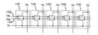
実際にDRAMには、上述したTFTを有する複数のメモリセルが、セルアレイに設けられている。図4を用いて、複数のメモリセルを有するセルアレイにおける、上記各動作について説明する。 Actually, in a DRAM, a plurality of memory cells having the above-described TFTs are provided in a cell array. Each of the above operations in a cell array having a plurality of memory cells will be described with reference to FIG.
まず図4(A)に、各メモリセルどうしの配線の接続を、一例として示す。図4(A)は、4つのメモリセル(Cell1、Cell2、Cell3、Cell4)を有するセルアレイの回路図であり、各メモリセルにはデータを記憶するためのTFT200が設けられている。なお図4(A)ではメモリセルが4つ設けられたセルアレイを示しているが、無論メモリセルの数はこれに限定されない。
First, FIG. 4A shows an example of wiring connection between memory cells. FIG. 4A is a circuit diagram of a cell array having four memory cells (Cell1, Cell2, Cell3, and Cell4). Each memory cell is provided with a
各メモリセルのTFT200は、2つのワード線WLb、WLfによって電位Vbg、Vfgが、ビット線BLによって電位Vdが、ソース線SLによって電位Vsが与えられている。なお各配線のレイアウトは、図4(A)に示した構成に限定されない。
In the
具体的に図4(A)では、メモリセル(Cell1)には、ワード線WLb1、WLf1、ビット線BL1、ソース線SL1が対応しており、メモリセル(Cell2)には、ワード線WLb1、WLf1、ビット線BL2、ソース線SL1が対応している。また、メモリセル(Cell3)には、ワード線WLb2、WLf2、ビット線BL1、ソース線SL2が対応しており、メモリセル(Cell4)には、ワード線WLb2、WLf2、ビット線BL2、ソース線SL2が対応している。 Specifically, in FIG. 4A, the memory cell (Cell1) corresponds to the word lines WLb1, WLf1, the bit line BL1, and the source line SL1, and the memory cell (Cell2) corresponds to the word lines WLb1, WLf1. , Bit line BL2 and source line SL1 correspond to each other. The memory cell (Cell3) corresponds to the word lines WLb2 and WLf2, the bit line BL1, and the source line SL2. The memory cell (Cell4) corresponds to the word lines WLb2 and WLf2, the bit line BL2 and the source line SL2. Is supported.
図4(B)に、タイミングチャートの一例として、一行目のメモリセル(Cell1)及び(Cell2)に対してリフレッシュ動作を行なう場合を示す。なお図4(B)では、図2を参考にして、各期間において各メモリセルに与えられる電位Vs、Vd、Vbg、Vfgの関係を示しているが、図3を参考にしていても良い。 FIG. 4B shows an example of a timing chart in which a refresh operation is performed on the memory cells (Cell1) and (Cell2) in the first row. Note that FIG. 4B shows the relationship between the potentials Vs, Vd, Vbg, and Vfg applied to each memory cell in each period with reference to FIG. 2; however, FIG. 3 may be referred to.
リフレッシュ動作は、メモリセルに格納された情報が時間と共に失われるのを防ぐために行なう。具体的には、メモリセルに格納された情報を一旦読み出して、その情報を再び同じメモリセルへ書き込む動作である。リフレッシュは、所定の期間ごとに行なう必要があり、本発明では、トランジスタのチャネル形成領域に蓄積された正孔がどれぐらい保持されるかによってその期間が決まってくる。また、本発明のリフレッシュ動作は、読み出し、パージ、書き込みという一連の動作によって行われる。パージは、トランジスタのチャネル形成領域に蓄積された正孔をすべて掃き出して、一旦メモリセルの状態をリセットする動作である。 The refresh operation is performed to prevent information stored in a memory cell from being lost with time. Specifically, this is an operation of once reading information stored in a memory cell and writing the information again to the same memory cell. The refresh needs to be performed every predetermined period, and in the present invention, the period is determined depending on how much the holes accumulated in the channel formation region of the transistor are held. The refresh operation of the present invention is performed by a series of operations of reading, purging, and writing. Purge is an operation of sweeping out all holes accumulated in a channel formation region of a transistor and once resetting the state of a memory cell.
なお、本発明において、パージ(パージを含むリフレッシュ)は、ワード線WLbを共有するメモリセル、つまり、メモリセル一行に対して同時に行われる。一方、書き込み、読み出しは、個々のメモリセルに対して行なうこともできるし、パージと同様に、メモリセル一行に対して同時に行なうこともできる。従って、読み出しや書き込みは、バス幅に合わせたビット数単位で行なう形態や、メモリセル一行単位で行なう形態が考えられるが、リフレッシュはメモリセル一行単位で行われる。また、多値データの格納はストレスに対して繊細であるため、書き込みや読み出しも一行ごとに行なうことが好ましい。 In the present invention, the purge (refresh including the purge) is simultaneously performed on the memory cells sharing the word line WLb, that is, on one row of the memory cells. On the other hand, writing and reading can be performed on individual memory cells, and can be performed on one row of memory cells at the same time as in the case of purging. Therefore, reading and writing can be performed in units of bits corresponding to the bus width or in units of memory cells in one row, but refresh is performed in units of memory cells in one row. Since storing multi-valued data is sensitive to stress, it is preferable that writing and reading be performed for each row.
最初に読み出されたデータは一旦ラッチ(図示せず)に格納され、パージ後にそのデータを再び書き込む。本実施の形態では、メモリセル(Cell1)には正孔が蓄積されない状態(前述した”0”の状態)、メモリセル(Cell2)には正孔が蓄積された状態(前述した”1”の状態)への書き込みが行われる。なお、書き込み時にはBL2によってメモリセル(Cell4)への電位も変化するが(書き込み時のストレス)、この電位変動によってメモリセル(Cell4)に蓄積された正孔に影響がないように電位を設定することが重要である。 The data read first is temporarily stored in a latch (not shown), and the data is written again after purging. In the present embodiment, a state where holes are not stored in the memory cell (Cell1) (the state of “0” described above), and a state where holes are stored in the memory cell (Cell2) (the state of “1” described above) State). At the time of writing, the potential to the memory cell (Cell4) also changes due to BL2 (stress at the time of writing). However, the potential is set so that the potential change does not affect the holes accumulated in the memory cell (Cell4). This is very important.
なお電源投入直後最初にデータを書き込む場合には、熱や静電気などによって既に電荷が蓄積されている場合も想定されるので、パージを行なってからデータの書き込みを行なうのが望ましい。 When writing data for the first time immediately after turning on the power, it is assumed that electric charges have already been accumulated due to heat, static electricity, or the like. Therefore, it is preferable to perform data writing after purging.
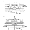
次に、DRAM混載の集積回路と画素部とを同一基板上に有する、発光装置の作製方法について説明する。ここでは、集積回路に積載されたDRAMに加え、OLEDに供給する電流を制御するTFTを例示して説明する。 Next, a method for manufacturing a light-emitting device in which an integrated circuit with a DRAM and a pixel portion are provided over the same substrate will be described. Here, a TFT that controls a current supplied to an OLED in addition to a DRAM mounted on an integrated circuit will be described as an example.
まず図5(A)に示すように、基板301の絶縁表面上に、本発明のDRAMの第1の電極302を形成する。第1の電極302は、Al、W、Mo、Ti、Taから選ばれた一種又は複数種からなる導電性の材料で形成することができる。本実施の形態ではWを用いたが、TaNの上にWを積層したものを第1の電極302として用いても良い。また、単層ではなく複数の層で構成されていても良い。
First, as shown in FIG. 5A, a
基板301には、例えばバリウムホウケイ酸ガラスや、アルミノホウケイ酸ガラスなどのガラス基板、石英基板、セラミック基板等を用いることができる。また、SUS基板を含む金属基板またはシリコン基板の表面に絶縁膜を形成したものを用いても良い。プラスチック等の可撓性を有する合成樹脂からなる基板は、一般的に上記基板と比較して耐熱温度が低い傾向にあるが、作製工程における処理温度に耐え得るのであれば用いることが可能である。
As the
次に、第1の電極302を覆うように第1の絶縁膜303を成膜する。本実施の形態では、第1の絶縁膜303は、2つの絶縁膜(第1の絶縁膜A 303a、第1の絶縁膜B 303b)を積層することで形成されている。第1の絶縁膜A 303aは酸窒化珪素膜を用い、10〜50nmの厚さで形成する。第1の絶縁膜B 303bは酸化珪素膜又は酸窒化珪素膜を用い、0.5〜1μmの厚さで形成する。なお第1の絶縁膜303はこの構成に限定されず、単層の絶縁膜で形成されていても良いし、3層以上の絶縁膜で形成されていても良い。また材料もこれに限定されない。
Next, a first
第1の絶縁膜303の表面(ここでは第1の絶縁膜B 303bの表面)は、先に形成した第1の電極302に起因する凹凸を有している場合がある。この場合、凹凸を平坦化する工程を設けることが望ましい。本実施の形態ではCMPを用いて平坦化を行なう。第1の絶縁膜303に対するCMPの研磨剤(スラリー)には、例えば、塩化シリコンガスを熱分解して得られるフュームドシリカ粒子をKOH添加水溶液に分散したものを用いると良い。CMPにより第1の絶縁膜を0.1〜0.5μm程度除去して、表面を平坦化する。
The surface of the first insulating film 303 (here, the surface of the first insulating
次に、第1の絶縁膜303の上に50nmの厚さの、非晶質半導体膜304をプラズマCVD法で形成する。非晶質半導体膜304は含有水素量にもよるが、好ましくは400〜550℃で数時間加熱して脱水素処理を行い、含有水素量を5atom%以下として、結晶化の工程を行なうことが望ましい。また、非晶質半導体膜をスパッタ法や蒸着法などの他の作製方法で形成しても良いが、膜中に含まれる酸素、窒素などの不純物元素を十分低減させておくことが望ましい。
Next, an
用いる半導体は珪素のみに限定されず、例えばシリコンゲルマニウムを用いることができる。シリコンゲルマニウムを用いる場合、ゲルマニウムの濃度は0.01〜4.5atomic%程度であることが好ましい。 The semiconductor used is not limited to silicon only, and for example, silicon germanium can be used. When silicon germanium is used, the concentration of germanium is preferably about 0.01 to 4.5 atomic%.
なお、第1の絶縁膜303と非晶質半導体膜304をいずれもプラズマCVD法で作製する場合、これらの2つの膜を大気に曝すことなく連続して形成しても良い。連続成膜することによって、大気による表面の汚染を極力抑え、よって作製されるTFTの特性バラツキを低減させることができる。
Note that in the case where both the first insulating
次に、非晶質半導体膜304への触媒の添加を行なう。本実施の形態では、重量換算で1〜100ppmのニッケルを含む酢酸ニッケル塩溶液をスピナーで塗布した。なお、酢酸ニッケル塩溶液の馴染みをよくするために、非晶質半導体膜304の表面をオゾン含有水溶液で処理することで極薄い酸化膜を形成し、その酸化膜をフッ酸と過酸化水素水の混合液でエッチングして清浄な表面を形成した後、再度オゾン含有水溶液で処理して極薄い酸化膜を形成しておいても良い。半導体膜の表面は本来疎水性なので、このように酸化膜を形成しておくことにより酢酸ニッケル塩溶液を均一に塗布することができる(図5(A))。
Next, a catalyst is added to the
勿論、非晶質半導体膜への触媒の添加は上記方法に限定されず、スパッタ法、蒸着法、プラズマ処理などを用いて添加するようにしても良い。 Needless to say, the addition of the catalyst to the amorphous semiconductor film is not limited to the above method, and may be performed by using a sputtering method, an evaporation method, a plasma treatment, or the like.
次に、500〜650℃で4〜24時間、例えば570℃、14時間の加熱処理を行った。加熱処理を施すことで、ニッケル含有層305により結晶化が進行し、結晶性の高められた結晶性半導体膜が形成される。
Next, heat treatment was performed at 500 to 650 ° C. for 4 to 24 hours, for example, 570 ° C. for 14 hours. By performing the heat treatment, crystallization proceeds with the nickel-containing
加熱処理の方法としては、電熱炉を用いるファーネスアニール法や、ハロゲンランプ、メタルハライドランプ、キセノンアークランプ、カーボンアークランプ、高圧ナトリウムランプ、高圧水銀ランプなどを用いたRTA法を用いることができる。または、加熱した不活性気体を用いるガス加熱方式のRTAを用いることも可能である。 As a heat treatment method, a furnace annealing method using an electric furnace or an RTA method using a halogen lamp, a metal halide lamp, a xenon arc lamp, a carbon arc lamp, a high-pressure sodium lamp, a high-pressure mercury lamp, or the like can be used. Alternatively, a gas heating type RTA using a heated inert gas can be used.
RTA法で行なう場合には、加熱用のランプ光源を1〜60秒、好ましくは30〜60秒点灯させ、それを1〜10回、好ましくは2〜6回繰り返す。ランプ光源の発光強度は任意なものとするが、非晶質半導体膜304が瞬間的には600〜1000℃、好ましくは650〜750℃程度にまで加熱されるようにする。このような高温になったとしても、半導体膜が瞬間的に加熱されるのみであり、基板301はそれ自身が歪んで変形することはない。
When the RTA method is used, the heating lamp light source is turned on for 1 to 60 seconds, preferably 30 to 60 seconds, and this is repeated 1 to 10 times, preferably 2 to 6 times. The emission intensity of the lamp light source is arbitrary, but the
その他の方法としてファーネスアニール法を用いる場合には、加熱処理に先立ち、500℃にて1時間程度の加熱処理を行い、非晶質半導体膜304が含有する水素を放出させておく。そして、電熱炉を用いて窒素雰囲気中にて550〜600℃、好ましくは580℃で4時間の加熱処理を行い、非晶質半導体膜304を結晶化させる。
In the case where the furnace annealing method is used as another method, heat treatment at 500 ° C. for about 1 hour is performed before the heat treatment to release hydrogen contained in the
なお、本実施の形態では触媒元素としてニッケル(Ni)を用いているが、その以外にも、ゲルマニウム(Ge)、鉄(Fe)、パラジウム(Pd)、スズ(Sn)、鉛(Pb)、コバルト(Co)、白金(Pt)、銅(Cu)、金(Au)といった元素を用いても良い。 In the present embodiment, nickel (Ni) is used as a catalyst element. In addition, germanium (Ge), iron (Fe), palladium (Pd), tin (Sn), lead (Pb), Elements such as cobalt (Co), platinum (Pt), copper (Cu), and gold (Au) may be used.
次に、結晶性半導体膜306内に存在する触媒元素のゲッタリングについて説明する。触媒元素を用いる結晶化により、結晶性半導体膜306内には、触媒元素(ここではニッケル)が平均的な濃度として1×10¹⁹/cm3を越える程度に残存しているものと考えられる。触媒元素が残留しているとTFTの特性に悪影響を及ぼす可能性があるため、触媒元素濃度を低減させる工程を設ける必要がある。
Next, gettering of a catalytic element existing in the
ゲッタリングの方法は様々であるが、本実施の形態では結晶性半導体膜306をパターニングする前に行なうゲッタリングの一例について説明する。まず、図5(B)に示すように結晶性半導体膜306の表面にバリア層307を形成する。バリア層307は、後にゲッタリングサイトを除去する際に、結晶性半導体膜306がエッチングされるのを防ぐために設ける。
There are various gettering methods. In this embodiment, an example of gettering performed before patterning the
バリア層307の厚さは1〜10nm程度とする。オゾン水で処理することにより形成されるケミカルオキサイドをバリア層として用いても良い。また、硫酸、塩酸、硝酸などと過酸化水素水を混合させた水溶液で処理しても同様にケミカルオキサイドを形成することができる。他には、酸化雰囲気中でのプラズマ処理する方法や、酸素含有雰囲気中での紫外線照射によりオゾンを発生させて酸化処理を行なう方法等を用いても良い。また、クリーンオーブンを用い、200〜350℃程度に加熱して薄い酸化膜を形成しバリア層としても良い。或いは、プラズマCVD法やスパッタ法、蒸着法などで1〜5nm程度の酸化膜を堆積してバリア層としても良い。いずれにしても、ゲッタリング工程時に、触媒元素がゲッタリングサイト側に移動できて、ゲッタリングサイトの除去工程時には、エッチング液がしみこまない(結晶性半導体膜306をエッチング液から保護する)膜、例えば、オゾン水で処理することにより形成されるケミカルオキサイド膜、酸化シリコン膜(SiOx)、または多孔質膜を用いればよい。
The thickness of the
次いで、バリア層307上にスパッタ法でゲッタリングサイト308として、膜中に希ガス元素を1×10²⁰/cm3以上の濃度で含むゲッタリング用の半導体膜(代表的には、非晶質シリコン膜)を25〜250nmの厚さで形成する。後に除去されるゲッタリングサイト308は結晶性半導体膜306とエッチングの選択比を大きくするため、密度の低い膜を形成することが好ましい。
Next, a gettering semiconductor film containing a rare gas element at a concentration of 1 × 10 20 / cm 3 or more (typically, an amorphous film) is formed on the
なお、希ガス元素は半導体膜中でそれ自体は不活性であるため、結晶性半導体膜306に悪影響を及ぼすことはない。また、希ガス元素としてはヘリウム(He)、ネオン(Ne)、アルゴン(Ar)、クリプトン(Kr)、キセノン(Xe)から選ばれた一種または複数種を用いる。
Note that the rare gas element itself is inactive in the semiconductor film, and thus does not adversely affect the
次に、加熱処理を施すことでゲッタリングを行なう(図5(B))。加熱処理はファーネスアニール法やRTA法で行なう。ファーネスアニール法で行なう場合には、窒素雰囲気中にて450〜600℃で0.5〜12時間の加熱処理を行なう。また、RTA法を用いる場合には、加熱用のランプ光源を1〜60秒、好ましくは30〜60秒点灯させ、それを1〜10回、好ましくは2〜6回繰り返す。ランプ光源の発光強度は任意なものとするが、半導体膜が瞬間的には600〜1000℃、好ましくは700〜750℃程度にまで加熱されるようにする。 Next, gettering is performed by performing a heat treatment (FIG. 5B). The heat treatment is performed by a furnace annealing method or an RTA method. In the case of performing the furnace annealing method, a heat treatment is performed at 450 to 600 ° C. in a nitrogen atmosphere for 0.5 to 12 hours. When the RTA method is used, a lamp light source for heating is turned on for 1 to 60 seconds, preferably 30 to 60 seconds, and this is repeated 1 to 10 times, preferably 2 to 6 times. Although the light emission intensity of the lamp light source is arbitrary, the semiconductor film is instantaneously heated to about 600 to 1000 ° C., preferably about 700 to 750 ° C.
加熱処理により、結晶性半導体膜306にある触媒元素が熱エネルギーにより放出され、拡散により矢印に示すようにゲッタリングサイト308に移動する。従って、ゲッタリングは処理温度に依存し、より高温であるほど短時間でゲッタリングが進むことになる。
By the heat treatment, the catalytic element in the
ゲッタリング工程終了後、ゲッタリングサイト308を選択的にエッチングして除去する。エッチングの方法としては、ClF3によるプラズマを用いないドライエッチング、或いはヒドラジンや、テトラエチルアンモニウムハイドロオキサイド(化学式 (CH3)4NOH)を含む水溶液などアルカリ溶液によるウエットエッチングで行なうことができる。この時バリア層307はエッチングストッパーとして機能する。また、バリア層307はその後フッ酸により除去する(図5(C))。
After the gettering step, the
次に、バリア層307除去後の結晶性半導体膜306をパターニングし、島状の半導体膜309、310を形成する(図5(D))。半導体膜309、310の膜厚は25〜100nm(好ましくは30〜60nm)とする。次に、半導体膜309、310を覆うように第2の絶縁膜311を成膜する。第2の絶縁膜311は、後の第2の電極を形成するために行なうドライエッチングにおいて、その膜厚が10〜40nm程度減少するので、その減少分を考慮に入れて膜厚を設定するのが望ましい。具体的には40〜150nm(より好ましくは60〜120nm)程度の厚さに第2の絶縁膜311を成膜する。
Next, the
第2の絶縁膜311には、例えば酸化珪素、窒化珪素または窒化酸化珪素等を用いることができる。本実施の形態では、第2の絶縁膜311を単層の絶縁膜で構成しているが、2層以上の複数の絶縁膜で構成されていても良い。また成膜方法は、プラズマCVD法、スパッタ法などを用いることができる。例えば、プラズマCVD法を用い、酸化珪素で第2の絶縁膜311を成膜する場合、TEOS(Tetraethyl Orthosilicate)とO2を混合したガスを用い、反応圧力40Pa、基板温度300〜400℃、高周波(13.56MHz)電力密度0.5〜0.8W/cm2とし、成膜する。
For the second
また窒化アルミニウムを第2の絶縁膜311として用いることができる。窒化アルミニウムは熱伝導率が比較的高く、TFTで発生した熱を効率的に発散させることができる。またアルミニウムの含まれない酸化珪素や酸化窒化珪素等を形成した後、窒化アルミニウムを積層したものを第2の絶縁膜311として用いても良い。
Alternatively, aluminum nitride can be used for the second
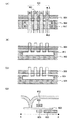
次に、第2の絶縁膜311上に導電膜を成膜する(図5(E))。本実施の形態ではTaNからなる第1の導電膜312aを20〜100nmの厚さで、Wからなる第2の導電膜312bを100〜400nmの厚さで成膜する。具体的に、第1の導電膜312aに用いるTaNは、ターゲットに純度99.99%のTaを用い、チャンバー内の温度を室温、Arの流量を50ml/min、N2の流量を10ml/min、チャンバー内の圧力0.6Pa、成膜電力1kWとし、成膜速度約40nm/minで成膜した。また第2の導電膜312bに用いるWは、ターゲットに純度99.99%のWを用い、チャンバー内の温度を230℃、Arの流量を100ml/min、チャンバー内の圧力1.5Pa、成膜電力6kWとし、成膜速度約390nm/minで成膜した。 Next, a conductive film is formed over the second insulating film 311 (FIG. 5E). In this embodiment mode, the first conductive film 312a made of TaN is formed with a thickness of 20 to 100 nm, and the second conductive film 312b made of W is formed with a thickness of 100 to 400 nm. Specifically, TaN used for the first conductive film 312a is Ta having a purity of 99.99% as a target, the temperature in the chamber is room temperature, the flow rate of Ar is 50 ml / min, and the flow rate of N 2 is 10 ml / min. The pressure in the chamber was set to 0.6 Pa, the film forming power was set to 1 kW, and the film was formed at a film forming speed of about 40 nm / min. As for W used for the second conductive film 312b, W having a purity of 99.99% is used as a target, the temperature in the chamber is 230 ° C., the flow rate of Ar is 100 ml / min, the pressure in the chamber is 1.5 Pa, and film formation is performed. At a power of 6 kW, a film was formed at a film formation speed of about 390 nm / min.
なお本実施の形態では、2層の導電膜を用いて第2の電極を形成する例について説明するが、導電膜は単層であっても良いし、また3層以上の複数の層で形成されていても良い。また各導電層の材料は本実施の形態に示したものに限定されない。 Note that in this embodiment, an example in which the second electrode is formed using a two-layer conductive film is described; however, the conductive film may be a single layer, or may be formed using three or more layers. It may be. The material of each conductive layer is not limited to those described in this embodiment mode.
具体的に各導電膜には、Ta、W、Ti、Mo、Al、Cuから選ばれた元素、または前記元素を主成分とする合金もしくは化合物で形成することができる。例えば1層目がTaで2層目がW、または1層目がTaNで2層目がAl、1層目がTaNで2層目がCuといった組み合わせも考えられる。また1層目と2層目のいずれか一方にAgPdCu合金を用いても良い。W、AlとSiの合金(Al−Si)、TiNを順次積層した3層構造としてもよい。Wの代わりに窒化タングステンを用いてもよいし、AlとSiの合金(Al−Si)に代えてAlとTiの合金膜(Al−Ti)を用いてもよいし、TiNに代えてTiを用いてもよい。ただし、複数の導電膜を成膜する場合、エッチング後に各層の導電膜の、チャネル長方向における幅に差を持たせたいならば、互いにエッチングの選択比のとれる材料を用いる。 Specifically, each conductive film can be formed of an element selected from Ta, W, Ti, Mo, Al, and Cu, or an alloy or compound containing the element as a main component. For example, a combination in which the first layer is Ta and the second layer is W, or the first layer is TaN and the second layer is Al, the first layer is TaN, and the second layer is Cu, is also conceivable. Further, an AgPdCu alloy may be used for one of the first layer and the second layer. It may have a three-layer structure in which W, an alloy of Al and Si (Al-Si), and TiN are sequentially stacked. Tungsten nitride may be used instead of W, an alloy film of Al and Ti (Al-Ti) may be used instead of an alloy of Al and Si (Al-Si), or Ti may be used instead of TiN. May be used. However, in the case of forming a plurality of conductive films, if it is desired to have a difference in the width of the conductive film of each layer in the channel length direction after the etching, materials having a selective etching ratio are used.
なお、導電膜の材料によって、適宜最適なエッチングガスを選択することが重要である。 Note that it is important to appropriately select an optimum etching gas depending on the material of the conductive film.
次にマスク314を形成し、図6(A)に示すように第1の導電膜312a及び第2の導電膜312bをエッチングする(第1のエッチング処理)。本実施の形態ではICP(Inductively Coupled Plasma:誘導結合型プラズマ)エッチング法を用いて行なった。エッチングガスとしてCl2とCF4とO2を混合したガスを用い、チャンバー内のエッチングガスの圧力を1.0Paとする。そして、コイル型の電極に500W、13.56MHzの高周波(RF)電力を投入し、プラズマを生成する。また基板が載置されたステージ(下部電極)に150W、13.56MHzの高周波(RF)電力を投入し、これにより基板に自己バイアス電圧が印加される。その後、エッチングガスをCl2とCF4に変更し、トータルの圧力を1.0Paとした。またコイル型の電極に500Wの高周波(13.56MHz)電力を投入し、基板側(試料ステージ)には20Wの高周波(13.56MHz)電力を投入した。
Next, a
CF4とCl2をエッチングガスとして用いると、第1の導電膜312aであるTaNと、第2の導電膜312bであるWのエッチングレートがほぼ等しくなり、共に同じ程度エッチングされる。 When CF 4 and Cl 2 are used as an etching gas, the etching rates of TaN, which is the first conductive film 312a, and W, which is the second conductive film 312b, are substantially equal, and both are etched to the same extent.
この第1のエッチング処理により、下層315aと上層315bとで構成された第1の形状の導電膜315と、下層316aと上層316bとで構成された第1の形状の導電膜316とが形成される。なおこの第1のエッチング処理において、下層315a、316aと上層315b、316bの側面がややテーパー状になる。また導電膜の残渣を残さないようにエッチングすると、第1の形状の導電膜315、316で覆われていない第2の絶縁膜311の表面が、5〜10nm程度またはそれ以上エッチングされることがある。
By this first etching treatment, a first-shaped
次に図6(B)に示すように、第1のエッチング処理で表面がエッチングされて幅が小さくなったマスク314を用い、第1の形状の導電膜315、316をエッチング(第2のエッチング処理)する。第2のエッチング処理でも第1のエッチング処理と同じくICPエッチング法を用いる。エッチングガスはSF6、Cl2、O2を混合したガスを用い、チャンバー内のエッチングガスの圧力を1.3Paとする。そして、コイル型の電極に700W、13.56MHzの高周波電力を投入し、プラズマを生成する。また基板が載置されたステージ(下部電極)に10W、13.56MHzの高周波電力を投入し、これにより基板に自己バイアス電圧が印加される。
Next, as shown in FIG. 6B, the first shape
SF6とCl2を混合したガスにO2を加えることで、Wのエッチングレートが増加し、また第1の形状の導電膜315、316の下層315b、316bを形成しているTaNのエッチングレートが極端に低下するため、選択比をとることができる。
By adding O 2 to a gas mixture of SF 6 and Cl 2 , the etching rate of W is increased, and the etching rate of TaN forming the
第2のエッチング処理によって、第2の形状の導電膜317(下層を317a、上層を317bとする)と、第2の形状の導電膜318(下層を318a、上層を318bとする)が形成される。上層317b、318bのチャネル長方向における幅は、下層317a、317bの幅よりも短くなっている。第2の形状の導電膜317は、DRAMの第2の電極として機能し、第2の形状の導電膜318は、OLEDに供給する電流を制御するTFTのゲート電極として機能する。なお第2のエッチング処理によって、第2の形状の導電膜317、318で覆われていない第2の絶縁膜311の表面が、5〜10nm程度またはそれ以上エッチングされる。
By the second etching treatment, a second shape conductive film 317 (the lower layer is 317a and the upper layer is 317b) and a second shape conductive film 318 (the lower layer is 318a and the upper layer is 318b) are formed. You. The width of the upper layers 317b and 318b in the channel length direction is shorter than the width of the
次に図6(B)に示すように、第2の形状の導電膜317、318をマスクとして用い、半導体膜309、310にn型の導電性を付与する不純物を添加する(第1のドーピング処理)。ドーピングはイオン注入法で行なう。ドーピングは、ドーズ量を1×10¹³〜5×10¹⁴atoms/cm2、加速電圧を40〜80kVとして行なう。n型を付与する不純物元素は、ドナーとして機能するP、As、Sb等の5族原子やS、Te、Se等の6族原子を用いるが、本実施の形態ではPを用いる。第1のドーピング処理により、自己整合的に第1の不純物領域320、321が形成される。第1の不純物領域320、321には1×1018〜1×1020atoms/cm3の濃度範囲でn型を付与する不純物元素が添加されている。
Next, as shown in FIG. 6B, an impurity imparting n-type conductivity is added to the
次に図6(C)に示すように、第2の形状の導電膜317、318の上層317b、318bをマスクとして、第2のドーピング処理を行なう。第2のドーピング処理では、第2の形状の導電膜317、318の下層317a、317aを不純物が通過するように、第1のドーピング処理よりも加速電圧を高くする。そして第2のドーピング処理によりLDD領域を形成するので、第1のドーピング処理よりもn型の不純物のドーズ量を下げる。具体的には、加速電圧を60〜120kVとし、ドーズ量を1×10¹³〜1×10¹⁵atoms/cm2とする。
Next, as shown in FIG. 6C, a second doping process is performed using the upper layers 317b and 318b of the
続いて、第2のドーピング処理より加速電圧を下げて第3のドーピング処理を行って、図6(C)の状態を得る。第3のドーピング処理は、加速電圧を50〜100kVとし、ドーズ量を1×10¹⁵〜1×10¹⁷atoms/cm2とする。第2のドーピング処理および第3のドーピング処理により、第2の形状の導電膜317、318の下層317a、317aと重なる第2の不純物領域322、323と、第1の不純物領域320、321に不純物がさらに添加されることで形成される第3の不純物領域324、325とが形成される。第2の不純物領域322、323には1×1018〜5×1019atoms/cm3の濃度範囲でn型を付与する不純物元素を添加され、第3の不純物領域324、325には1×1019〜5×1021atoms/cm3の濃度範囲でn型を付与する不純物元素が添加される。
Subsequently, a third doping process is performed at a lower acceleration voltage than in the second doping process to obtain the state in FIG. In the third doping process, the acceleration voltage is set to 50 to 100 kV and the dose is set to 1 × 10 15 to 1 × 10 17 atoms / cm 2 . By the second doping process and the third doping process, the
第2の不純物領域322、323は第3の不純物領域324、325の内側に形成されており、第2の不純物領域322、323はLDD領域、第3の不純物領域324、325はソース/ドレイン領域として機能する。
The
もちろん、適当な加速電圧にすることで、第2のドーピング処理および第3のドーピング処理を1回のドーピング処理で済まし、低濃度不純物領域および高濃度不純物領域を形成することも可能である。 Needless to say, by setting the appropriate acceleration voltage, the second doping process and the third doping process can be performed by one doping process, and a low-concentration impurity region and a high-concentration impurity region can be formed.
なお、pチャネル型のTFTが形成される島状の半導体膜310には、図6(B)、図6(C)に示した第2、第3のドーピング処理によりn型の不純物をドーピングする必要はないため、n型の不純物のドーピングの際に、マスクで覆っておいても良い。また、マスク数削減のために敢えてマスクを設けず、p型の導電型を付与する不純物の濃度を高くして、島状の半導体膜の極性をp型に反転させても良い。本実施の形態では、島状の半導体膜の極性をp型に反転させる場合について説明する。
Note that the island-shaped
図6(D)に示すように、レジストからなるマスク326でnチャネル型の島状の半導体膜309を覆い、島状の半導体膜310にp型の導電型を付与する不純物をドーピングする(第4のドーピング処理)。この第4のドーピング処理において、第2の形状の導電膜317、318の上層317b、318bがマスクとして機能し、pチャネル型TFTに用いる島状の半導体膜310にp型を付与する不純物元素が添加された第4の不純物領域327が形成される。本実施の形態ではジボラン(B2H6)を用いたイオンドープ法で形成する。第4の不純物領域は、実際には第2の形状の導電膜317、318の下層317a、318aと重なる領域と、それ以外の領域とで、p型を付与する不純物元素及びn型を付与する不純物領域の濃度が異なっている。しかしいずれの領域においても、p型を付与する不純物元素の濃度が2×10²⁰〜2×10²¹atoms/cm3となるようにドーピング処理することで、p型が優勢となるため、pチャネル型TFTのソース領域およびドレイン領域として機能するのに何ら問題は生じない。
As shown in FIG. 6D, the n-channel island-shaped
以上までの工程でそれぞれの島状の半導体膜に不純物領域が形成される。 Through the above steps, impurity regions are formed in the respective island-shaped semiconductor films.
次に、島状の半導体膜309、310と、第2の絶縁膜311と、第2の形状の導電膜317、318と覆って、第1の層間絶縁膜330を成膜する(図7(A))。第1の層間絶縁膜330は、珪素を含む酸化珪素、窒化珪素、酸化窒化珪素などの絶縁膜を用いることができ、その厚さは100〜200nm程度とする。
Next, a first
次に、島状の半導体膜309、310に添加された不純物元素を活性化するために、熱処理を行なう。この工程はファーネスアニール炉を用いる熱アニール法、レーザーアニール法、またはラピッドサーマルアニール法(RTA法)を用いることができる。例えば熱アニール法で活性化を行なう場合、酸素濃度が1ppm以下、好ましくは0.1ppm以下の窒素雰囲気中で、400〜700℃(好ましくは500〜600℃)で行なう。さらに、3〜100%の水素を含む雰囲気中で、300〜450℃で1〜12時間の熱処理を行い、島状の半導体膜を水素化する工程を行なう。この工程は、熱的に励起こされた水素によりダングリングボンドを終端する目的で行なわれる。水素化の他の手段として、プラズマ水素化(プラズマにより励起こされた水素を用いる)を行っても良い。また活性化処理は第1の層間絶縁膜330を成膜する前に行っても良い。
Next, heat treatment is performed to activate the impurity elements added to the island-shaped
上記一連の工程によって、DRAMとして用いるnチャネル型TFT331と、OLEDに供給する電流を制御するpチャネル型TFT332を形成することができる。
Through the above series of steps, an n-
また本実施の形態では、LDD領域として機能する第2の不純物領域322全体が、第2の形状の導電膜317、318の下層317a、318aと重なっているが、本発明はこれに限定されない。例えば、第1のエッチング処理と第2のエッチング処理の間にドーピング処理を行なってソース/ドレイン領域を形成し、なおかつ第2のエッチング処理で下層をチャネル長方向において短くなるようにエッチングすることで、第2の形状の導電膜317、318の下層317a、318aと重なる領域と、それ以外の領域を、両方形成することができる。
In this embodiment mode, the entire
なお上記プラズマエッチングはICPエッチング法に限定されない。例えば、ECR(Electron Cyclotron Resonance:電子サイクロトロン共鳴)エッチング法、RIEエッチング法、ヘリコン波エッチング法、ヘリカル共鳴エッチング法、パルス変調エッチング法やその他のプラズマエッチング法を用いていても良い。 The plasma etching is not limited to the ICP etching method. For example, an ECR (Electron Cyclotron Resonance) etching method, an RIE etching method, a helicon wave etching method, a helical resonance etching method, a pulse modulation etching method, or another plasma etching method may be used.
本実施の形態では、触媒元素による結晶化方法のみを用いた例を示したが、本発明はこれに限定されない。触媒元素を用いて結晶化を行なった後に、より結晶性を高めるために、パルス発振のレーザ光照射を行なうようにしても良い。また本発明において用いるゲッタリング工程は、本実施の形態に示した方法に限定されない。その他の方法を用いて半導体膜中の触媒元素を低減するようにしても良い。例えば、特開平10−135468号公報または特開平10−135469号公報に記載されているように、触媒元素をリンのゲッタリング作用を用いて除去するようにしても良い。 In the present embodiment, an example using only a crystallization method using a catalytic element has been described, but the present invention is not limited to this. After crystallization using a catalytic element, pulsed laser light irradiation may be performed in order to further improve crystallinity. Further, the gettering step used in the present invention is not limited to the method described in this embodiment. The catalyst element in the semiconductor film may be reduced by using another method. For example, as described in JP-A-10-135468 or JP-A-10-135469, the catalytic element may be removed by using the gettering action of phosphorus.
次に、第1の層間絶縁膜330を覆うように、第2の層間絶縁膜333と第3の層間絶縁膜を成膜する。本実施の形態では、第2の層間絶縁膜333を有機樹脂、例えば非感光性のアクリルを用いて形成する。第3の層間絶縁膜334は、水分や酸素などのOLEDの劣化を促進させる原因となる物質を、他の絶縁膜と比較して透過させにくい膜を用いる。代表的には、例えばDLC膜、窒化炭素膜、RFスパッタ法で形成された窒化珪素膜等を用いるのが望ましい。
Next, a second
次いで、第2の絶縁膜311、第1の層間絶縁膜330、第2の層間絶縁膜333及び第3の層間絶縁膜334をエッチングし、コンタクトホールを形成する。そして、島状の半導体膜309、310とコンタクトを形成する配線335〜338を形成する。
Next, the second
次に、第3の層間絶縁膜334及び配線335〜338を覆って透明導電膜を成膜し、パターニングすることで、pチャネル型TFT332の島状の半導体膜310とコンタクトを形成している配線338に接続した、画素電極(陽極)340を形成する(図7(B))。画素電極340に用いる透明導電膜は、ITOのみならず、酸化インジウムに2〜20%の酸化亜鉛(ZnO)を混合した透明導電膜を用いても良い。画素電極340は、その表面が平坦化されるように、CMP法、ポリビニルアルコール系の多孔質体を用いた拭浄で研磨しても良い。またCMP法を用いた研磨後に、画素電極340の表面に紫外線照射、酸素プラズマ処理などを行ってもよい。
Next, a transparent conductive film is formed so as to cover the third interlayer insulating film 334 and the
そして、隔壁として用いる有機樹脂膜341を、第3の層間絶縁膜334上に形成する。有機樹脂膜341は、画素電極340と重なる領域において開口部を有するようにする。有機樹脂膜341は、次に電界発光層を成膜する前に、吸着した水分や酸素等を除去するために真空雰囲気下で加熱しておく。具体的には、100℃〜200℃、0.5〜1時間程度、真空雰囲気下で加熱処理を行なう。望ましくは3×10⁻⁷Torr以下とし、可能であるならば3×10⁻⁸Torr以下とするのが最も望ましい。そして、有機樹脂膜341に真空雰囲気下で加熱処理を施した後に電界発光層を成膜する場合、成膜直前まで真空雰囲気下に保つことで、信頼性をより高めることができる。
Then, an
有機樹脂膜341の開口部における端部は、該端部において後に成膜される電界発光層に穴があかないように、丸みを帯びさせることが望ましい。具体的には、開口部における有機樹脂膜341の断面が描いている曲線の曲率半径が、0.2〜2μm程度であることが望ましい。
It is desirable that the end of the opening of the
図7(C)では、有機樹脂膜341として、ポジ型の感光性のアクリル樹脂を用いた例を示している。感光性の有機樹脂には、光、電子、イオンなどのエネルギー線が露光された箇所が除去されるポジ型と、露光された箇所が残るネガ型とがある。本発明ではネガ型の有機樹脂膜を用いても良い。また感光性のポリイミドを用いて有機樹脂膜341を形成しても良い。
FIG. 7C illustrates an example in which a positive photosensitive acrylic resin is used for the
ネガ型のアクリルを用いて有機樹脂膜341を形成した場合、開口部における端部が、S字状の断面形状となる。このとき開口部の上端部及び下端部における曲率半径は、0.2〜2μmとすることが望ましい。
In the case where the
上記構成により、後に形成される電界発光層や陰極のカバレッジを良好とすることができ、画素電極340と陰極が電界発光層に形成された穴においてショートするのを防ぐことができる。また電界発光層の応力を緩和させることで、発光領域が減少するシュリンクとよばれる不良を低減させることができ、信頼性を高めることができる。
With the above structure, coverage of an electroluminescent layer and a cathode formed later can be improved, and a short circuit between the
次に、画素電極340上に電界発光層342を成膜する。電界発光層342は、単数または複数の層からなり、有機物のみならず無機物の層が含まれていても良い。
Next, an
次に、電界発光層342を覆って、陰極343を成膜する。陰極343は、仕事関数の小さい導電膜であれば公知の他の材料を用いることができる。例えば、Ca、Al、CaF、MgAg、AlLi等が望ましい。
Next, a
画素電極340、電界発光層342、陰極343は、有機樹脂膜341の開口部において重なり合っており、該重なり合っている部分がOLED344に相当する。
The
次に、有機樹脂膜341及び陰極343上に、保護膜345が成膜されている。保護膜345は第3の層間絶縁膜334と同様に、水分や酸素などのOLEDの劣化を促進させる原因となる物質を、他の絶縁膜と比較して透過させにくい膜を用いる。代表的には、例えばDLC膜、窒化炭素膜、RFスパッタ法で形成された窒化珪素膜等を用いるのが望ましい。また上述した水分や酸素などの物質を透過させにくい膜と、該膜に比べて水分や酸素などの物質を透過させやすい膜とを積層させて、保護膜として用いることも可能である。
Next, a
なお図7(C)では、OLEDから発せられる光が基板301側に照射される構成を示しているが、光が基板とは反対側に向かうような構造のOLEDとしても良い。
Note that FIG. 7C illustrates a structure in which light emitted from the OLED is irradiated to the
なお、実際には図7(C)まで完成したら、さらに外気に曝されないように気密性が高く、脱ガスの少ない保護フィルム(ラミネートフィルム、紫外線硬化樹脂フィルム等)や透光性のカバー材でパッケージング(封入)することが好ましい。その際、カバー材の内部を不活性雰囲気にしたり、内部に吸湿性材料(例えば酸化バリウム)を配置したりするとOLEDの信頼性が向上する。 Actually, when completed up to FIG. 7C, a protective film (laminate film, ultraviolet curable resin film, etc.) having high airtightness and less degassing so as not to be further exposed to the outside air, or a light-transmitting cover material is used. Packaging (encapsulation) is preferred. At this time, the reliability of the OLED is improved by setting the inside of the cover material to an inert atmosphere or arranging a hygroscopic material (for example, barium oxide) inside.
上述した作製方法を用いることで、DRAMの記憶素子として用いられるnチャネル型TFT331と、画素部に形成されるpチャネル型TFTとを同一基板上に形成することができる。
By using the above manufacturing method, an n-
なお、DRAMを含む集積回路と、画素部とを基板上に形成した後、該集積回路と画素部を基板から剥離し、別の基板に転写するようにしても良い。転写は、基板と集積回路及び画素部の間に金属酸化膜を設け、該金属酸化膜を結晶化により脆弱化して集積回路及び画素部を剥離し、転写する方法、基板と集積回路及び画素部の間に水素を含む非晶質珪素膜を設け、レーザ光の照射またはエッチングにより該非晶質珪素膜を除去することで基板と集積回路及び画素部とを剥離し、転写する方法、集積回路及び画素部が形成された基板を機械的に削除または溶液やガスによるエッチングで除去することで集積回路及び画素部を基板から切り離し、転写する方法等、様々な方法を用いることができる。いずれの方法を用いる場合でも、転写は、画素部において表示素子の形成が完了する前に行なうのが良い。例えば液晶表示装置の場合は対向電極を貼り合わせて液晶を注入する前、発光装置の場合は電界発光層を成膜する前に行なうのが望ましい。 Note that after an integrated circuit including a DRAM and a pixel portion are formed over a substrate, the integrated circuit and the pixel portion may be separated from the substrate and transferred to another substrate. The transfer is performed by providing a metal oxide film between the substrate, the integrated circuit, and the pixel portion, weakening the metal oxide film by crystallization to peel off the integrated circuit and the pixel portion, and transferring the substrate, the integrated circuit, and the pixel portion A method for transferring and transferring a substrate and an integrated circuit and a pixel portion by providing an amorphous silicon film containing hydrogen between the substrates and removing the amorphous silicon film by laser light irradiation or etching to transfer the integrated circuit, Various methods can be used, such as a method in which the integrated circuit and the pixel portion are separated from the substrate and transferred by mechanically removing the substrate on which the pixel portion is formed or removing the substrate by etching with a solution or a gas. In any case, the transfer is preferably performed before the formation of the display element in the pixel portion is completed. For example, in the case of a liquid crystal display device, it is desirable to carry out before the liquid crystal is injected by laminating the counter electrode, and in the case of the light emitting device, it is desirable to carry out before the electroluminescent layer is formed.
なお本発明の半導体表示装置は、必ずしも本実施の形態に示す発光装置に限定されない。上述した発光装置は本発明の一実施形態について具体的に説明しただけであり、本発明は、上述した実施の形態に限定されるものではなく、発明の技術的思想に基づく各種の変形が可能である。 Note that the semiconductor display device of the present invention is not necessarily limited to the light-emitting device described in this embodiment. The above-described light-emitting device is only specifically described for one embodiment of the present invention, and the present invention is not limited to the above-described embodiment, and various modifications based on the technical idea of the invention are possible. It is.
上述した通り本発明では、薄膜トランジスタにデータを記憶することができるので、キャパシタを別途設ける必要がなく、メモリセルの面積を抑えることができる。よって、コストを抑えつつ、DRAM混載の集積回路の高集積化、大容量化を実現することができる。そして集積回路の高集積化、大容量化の実現により、フラットパネルディスプレイの画素部と同じ基板上に一体形成することが可能な、集積回路の範囲を広げることができ、システムオンパネルの高機能化を実現することができる。 As described above, in the present invention, data can be stored in the thin film transistor; therefore, there is no need to separately provide a capacitor, and the area of the memory cell can be reduced. Therefore, high integration and large capacity of an integrated circuit with embedded DRAM can be realized while suppressing cost. By realizing high integration and large capacity of integrated circuits, the range of integrated circuits that can be integrally formed on the same substrate as the pixel portion of the flat panel display can be expanded, and the high performance of the system-on-panel Can be realized.
次に、各メモリセルに記憶素子として用いるTFTに加えて、スイッチング素子として用いるTFTを設ける、DRAMの一例について説明する。 Next, an example of a DRAM in which a TFT used as a switching element is provided in each memory cell in addition to a TFT used as a storage element will be described.
本実施例のDRAMが有するセルアレイの回路図を、図8(A)に一例として示す。図8(A)は、4つのメモリセル(Cell1,Cell2,Cell3,Cell4)を有するセルアレイの回路図であり、各メモリセルには記憶素子として機能するTFT800と、スイッチング素子として機能するTFT801が設けられている。なお図8(A)ではメモリセルが4つ設けられたセルアレイを示しているが、無論メモリセルの数はこれに限定されない。
FIG. 8A shows an example of a circuit diagram of a cell array included in the DRAM of this embodiment. FIG. 8A is a circuit diagram of a cell array including four memory cells (Cell1, Cell2, Cell3, and Cell4). Each memory cell includes a
各メモリセルのTFT800には、2つのワード線WLb、WLfによって電位Vbg、Vfgが、ソース線SLによって電位Vsが与えられている。またビット線BLからの電位Vdの供給が、TFT801によって制御されている。TFT801のスイッチングは、選択線SeLからそのゲート電極に供給される電位によって制御される。なお各配線のレイアウトは、図8(A)に示した構成に限定されない。そしてこれらの配線に加えて、さらに別の配線が各メモリセルに設けられていても良い。
The potentials Vbg and Vfg are supplied to the
TFT801はスイッチング素子として機能するので、導電型に特に限定はなく、n型であってもp型であってもどちらでも良い。そして、TFT801は、書き込み、読み出し、パージの際にオンに、保持の際にはオフになるように動作させる。
Since the
本実施例のように、スイッチング素子として用いるTFTを設けることで、メモリセルの選択性が向上する。具体的には、メモリセル(Cell1)に書き込みを行なうためにBL1に5V印加される場合の同列のメモリセル(Cell3)を考える。この場合、スイッチング素子がないと、メモリセル(Cell3)を構成するTFTのソースドレイン間には電位差が生じ、メモリセル(Cell3)の状態に影響を与えるおそれがある(書き込み時のストレス)。一方、スイッチング素子がオフの状態では、そのような電位差が生じないため、メモリセル(Cell3)へはストレスがかからない。その結果、ストレスによる誤動作の低減や、リフレッシュ間隔の向上が可能となる。 By providing a TFT used as a switching element as in this embodiment, selectivity of a memory cell is improved. Specifically, a memory cell (Cell3) in the same column when 5 V is applied to BL1 in order to write to the memory cell (Cell1) is considered. In this case, if there is no switching element, a potential difference occurs between the source and the drain of the TFT constituting the memory cell (Cell3), which may affect the state of the memory cell (Cell3) (stress at the time of writing). On the other hand, when the switching element is off, no such potential difference occurs, so that no stress is applied to the memory cell (Cell3). As a result, it is possible to reduce malfunction due to stress and to improve the refresh interval.
また、スイッチング素子を有さない場合には、ソース線を一行ごとに独立に制御していたのに対し、スイッチング素子を有することで非選択メモリセルのソースドレイン間の余計な電位差を除去することが可能となるため、全てのソース線電位を共通にすることが可能となる。その結果、駆動回路を単純にしたり、ソース線の面積を削減したりすることが可能となる。 In addition, when the switching element was not provided, the source line was controlled independently for each row, but by having the switching element, an unnecessary potential difference between the source and the drain of the unselected memory cell was removed. Therefore, all the source line potentials can be made common. As a result, the driving circuit can be simplified and the area of the source line can be reduced.
なお、TFT800において効率よくインパクトイオン化を起こすためには、或いは読み出し時においてTFT800の電流値の差をより効率よく読み出すためには、選択時のTFT801のゲート電極の電位VgsをTFT800のゲート電極の電位Vgsより大きめにすることが好ましい。
Note that in order to cause impact ionization in the
また、TFT800とTFT801が共にnチャネル型であるならば、敢えて選択線SeLとワード線WLfとを共通の配線にし、電源数を抑えるようにしても良い。さらにこの場合、TFT800とTFT801の活性層を連続させることで、1つのTFTとすることができる。図8(B)に、TFT800とTFT801の活性層を互いに連続させることで得られる、TFT500の断面図を示す。
If both the
図8(B)において、501は活性層であり、チャネル形成領域502、ソース領域503、ドレイン領域504を有する。また505は第1の電極、506は第2の電極、507は第1の絶縁膜、508は第2の絶縁膜に相当する。第1の電極505は活性層501を間に挟んで第2の電極506と重なっている。そして、第1の電極505は第1の絶縁膜507を間に挟んでチャネル形成領域502と重なっている。また第2の電極506は、第2の絶縁膜508を間に挟んでチャネル形成領域502と重なっている。
In FIG. 8B,
そして図8(B)では、第1の電極505はチャネル形成領域502の一部とのみ重なっており、チャネル形成領域502のドレイン領域504には、第1の電極505とは重ならず、第2の電極506と重なる領域が存在する。このようにワード線WLfと選択線SeLを共通化し、また活性層を連続させる事で、TFTを2つ設ける場合よりも、メモリセルの面積を抑えることができ、なおかつTFTを2つ設けた場合と同様に、電荷の保持を確実に行なうことができる。
In FIG. 8B, the
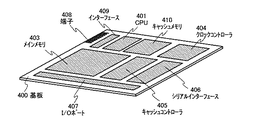
本実施例では、本発明の集積回路に積載されたDRAMのメモリセルの構成について説明する。 In this embodiment, a configuration of a memory cell of a DRAM mounted on an integrated circuit of the present invention will be described.
図9(A)に、本実施例のメモリセルの上面図を示す。図9(A)に示すメモリセルには、記憶素子として機能するTFT901が設けられている。そして、902はビット線BL、903はソース線SL、904はワード線WLfに相当する。図9(A)に示すように、本実施例では、ソース線SL903がワード線WLb906と同一の導電膜をパターニングすることで得られる。
FIG. 9A shows a top view of the memory cell of this embodiment. The memory cell illustrated in FIG. 9A includes a
図9(B)は、図9(A)に示した上面図のうち、最も最上層に設けられたビット線BL902が形成される前の、メモリセルの上面図に相当する。905はTFT901が有する活性層に相当する。ワード線WLf904の一部は第2の絶縁膜(図示せず)を間に挟んで活性層905と重なっており、第2の電極として機能している。本実施例でワード線WLf904は、活性層905と、ビット線BL902との間の層に設けられている。
FIG. 9B corresponds to a top view of the memory cell before the bit line BL902 provided in the uppermost layer is formed in the top view shown in FIG. 9A. 905 corresponds to the active layer of the
図9(C)は、図9(B)に示した上面図のうち、ワード線WLf904が形成される前の、メモリセルの上面図に相当する。ワード線WLb906の一部は第1の絶縁膜(図示せず)を間に挟んで活性層905と重なっており、第1の電極として機能している。本実施例でソース線SL903及びワード線WLb906は、活性層905よりも下の層(基板側)に設けられている。
FIG. 9C corresponds to the top view of the memory cell before the word line WLf904 is formed in the top view illustrated in FIG. 9B. Part of the word line WLb906 overlaps with the
図9(D)に、図9(A)のA−A’における断面図を示す。図9(D)に示すようにワード線WLf904とワード線WLb906は、活性層905を間に挟んで重なっている。なお本実施例ではソース線SL903をワード線WLb906と同じ導電膜から形成しているが、ソース線SL903をビット線BL902より上部の導電膜で形成しても良い。
FIG. 9D is a cross-sectional view taken along a line A-A ′ in FIG. As shown in FIG. 9D, the word line WLf904 and the word line WLb906 overlap with the
なお、ソース線の電位を固定にする場合、異なるワード線を有する隣り合ったメモリセルどうしで、共通のソース線を有していても良い。図11に、図9とは異なる本発明のメモリセルの上面図を示す。図11にはメモリセル1000a、1000bがレイアウトされており、1001はビット線BL、1002はソース線SL、1003はワード線WLfに相当する。図11ではメモリセル1000a、1000bで活性層1004とビット線BL1001を共有している。なお図11に示す上面図では図示されないが、活性層1004の下層においてワード線WLf1003と重なる領域に、ワード線WLbが設けられている。図11に示すように活性層またはソース線を隣り合うメモリセルで共有することによって、レイアウトの面積をより縮小することができる。
When the potential of the source line is fixed, adjacent memory cells having different word lines may have a common source line. FIG. 11 shows a top view of a memory cell of the present invention which is different from FIG. In FIG. 11,
本実施例では、本発明の集積回路の一つであるマイクロプロセッサの構成について説明する。 In this embodiment, a configuration of a microprocessor which is one of the integrated circuits of the present invention will be described.
図10に、本実施例のマイクロプロセッサの斜視図を示す。図10に示すマイクロプロセッサは、基板400上に、CPU401、メインメモリ403、クロックコントローラ404、キャッシュコントローラ405、シリアルインターフェース406、I/Oポート407、端子408、インターフェース409、キャッシュメモリ410等が形成されている。勿論、図10に示すマイクロプロセッサは、その構成を簡略化して示した一例にすぎず、実際のマイクロプロセッサはその用途によって多種多様な構成を有している。
FIG. 10 is a perspective view of the microprocessor of the present embodiment. In the microprocessor illustrated in FIG. 10, a
CPU401をより高速に動作させるには、それに見合う程度の高速なメモリを必要とする。しかし、CPU401の動作スピードにあったアクセスタイムをもつ高速の大容量メモリを使用した場合、一般的にコストが高くなってしまう。そこで大容量のメインメモリ403の他に、メインメモリ403よりも小容量であるが高速のメモリであるキャッシュメモリ410を、CPU401とメインメモリ403の間に介在させる。CPU401がキャッシュメモリ410にアクセスすることにより、メインメモリ403のスピードによらず、高速で動作することが可能となる。
In order to operate the
本発明の集積回路では、メインメモリ403に低コスト化、大容量化に優れるDRAMを用い、キャッシュメモリ410には高速な動作が可能なSRAMを用いる。
In the integrated circuit of the present invention, a DRAM which is excellent in cost reduction and large capacity is used for the
なおメインメモリ403には、CPU401で実行されるプログラムが格納されている。そして例えば実行初期において、メインメモリ403に格納されているプログラムは、キャッシュメモリ410にダウンロードされる。ダウンロードされるプログラムは、メインメモリ403に格納されているものに限定されず、他の外付のメモリからダウンロードすることもできる。キャッシュメモリ410は、CPU401で実行されるプログラムを格納するだけでなく、ワーク領域としても機能し、CPU401の計算結果等を一時的に格納する。
Note that a program executed by the
なおCPUは単数に限られず、複数設けていても良い。CPUを複数設け、並列処理を行なうことで、動作速度の向上を図ることができる。その場合、CPU間の処理速度がまちまちだと処理全体で見たときに不都合が起きる場合があるので、スレーブとなる各CPUの処理速度のバランスを、マスターとなるCPUでとるようにしても良い。 Note that the number of CPUs is not limited to one, and a plurality of CPUs may be provided. By providing a plurality of CPUs and performing parallel processing, the operation speed can be improved. In this case, if the processing speed between the CPUs is different, inconvenience may occur when the entire processing is viewed. Therefore, the processing speeds of the slave CPUs may be balanced by the master CPU. .
なお本実施例では集積回路としてマイクロプロセッサを例示したが、本発明の集積回路に用いられるDRAMは、マイクロプロセッサのメインメモリにその用途が限られるわけではない。例えば表示装置の駆動回路に用いられるビデオラムや、画像処理回路に必要となる大容量メモリとしての用途も好ましい。その他、様々なシステムLSIにおいても、大容量もしくは小型用途のメモリとして用いることができる。 In this embodiment, a microprocessor is exemplified as an integrated circuit. However, the application of the DRAM used in the integrated circuit of the present invention is not limited to the main memory of the microprocessor. For example, it is also preferable to use it as a video RAM used for a drive circuit of a display device or as a large-capacity memory required for an image processing circuit. In addition, it can be used as a large-capacity or small-sized memory in various system LSIs.
本実施例では、共通の配線から複数のメモリセルに電位Vbgが与えられる場合の、具体的な書き込みの手順について、説明する。 In this embodiment, a specific writing procedure in the case where the potential Vbg is applied to a plurality of memory cells from a common wiring will be described.
図12に、本実施例のセルアレイの一部を、回路図で示す。図12に示す全てのメモリセル1101〜1105には、共通の配線1106から第1のゲート電極の電位Vbgが与えられる。またメモリセル1101〜1105には、共通の配線1107から第2のゲート電極の電位Vfgが与えられる。そして図12では、メモリセル1101〜1105を用いて3値のデータを書き込むものとする。
FIG. 12 is a circuit diagram showing a part of the cell array according to the present embodiment. All the
具体的にメモリセル1101〜1105に書き込むデータは、順に”0、1、0、2、1”とする。そして”0”のデータは、ドレイン電圧をインパクトイオン化の閾値電圧よりも低い場合に、”1”と”2”のデータは、インパクトイオン化により正孔を蓄積する場合に対応し、”2”のデータの電荷の蓄積量は、”1”のデータの電荷の蓄積量よりも高いものとする。
Specifically, the data to be written to the
まず1回目の書き込み時には、データ”0”に対応するメモリセル1101、1103において、ドレイン電圧をインパクトイオン化の閾値電圧よりも低くする。またデータ”1”に対応するメモリセル1102、1104、1105において、ドレイン電圧をインパクトイオン化の閾値電圧よりも高くする。上記動作により、メモリセル1101、1103、1104では電荷の蓄積が行なわれず、メモリセル1102、1105ではデータ”1”に見合った量の正孔が蓄積される。具体的にTFTに与えられる電位Vdは、各メモリセル1101〜1105においてそれぞれ2V、5V、2V、2V、5Vとする。そして全てのメモリセル1101〜1105において、TFTに与えられる電位Vsを0V、電位Vfgを3V、電位Vbgを−4Vとする。
First, at the time of the first writing, in the
次に2回目の書き込み時には、データ”0”と”1”に対応するメモリセル1101、1102、1103、1105において、ドレイン電圧をインパクトイオン化の閾値電圧よりも低くする。そして、データ”2”に対応するメモリセル1105において、ドレイン電圧をインパクトイオン化の閾値電圧よりも高くする。このとき、配線1107に与えられる電位Vbgは、1回目の書き込み時よりも低くし、メモリセル1105に蓄積される電荷の量が1回目の書き込み時よりも増えるようにする。上記動作により、メモリセル1101、1103にはデータ”0”が、またメモリセル1102、1105にはデータ”1”が保持されたまま、メモリセル1104にはデータ”2”に見合った量の正孔が蓄積される。具体的にTFTに与えられる電位Vdは、各メモリセル1101〜1105においてそれぞれ2V、2V、2V、5V、2Vとする。そして全てのメモリセル1101〜1105において、TFTに与えられる電位Vsを0V、電位Vfgを3V、電位Vbgを−6Vとする。
Next, at the time of the second writing, in each of the
なお本発明は、必ずしも正孔の蓄積量の少ないメモリセルから順に書き込みを行なう必要はない。 Note that, in the present invention, it is not always necessary to perform writing sequentially from the memory cell having the smaller hole accumulation amount.
また、本実施例では3値のデータを記憶するためのDRAMの場合について説明したが、データの値をn(nは3以上の自然数)と一般化すると、書き込みの回数は(n−1)回と表される。 In this embodiment, the case of a DRAM for storing ternary data is described. However, when the data value is generalized to n (n is a natural number of 3 or more), the number of times of writing is (n-1). Represented as times.
本実施例では、メモリセルからデータを読み出すための手段について説明する。本実施例では3値のデータを読み出す場合について説明するが、本実施例ではこれに限定されず、4値以上のデータの読み出しにも対応させることができる。 In this embodiment, a means for reading data from a memory cell will be described. In this embodiment, a case where ternary data is read will be described. However, the present embodiment is not limited to this, and it is possible to read four or more values of data.
図13(A)に、メモリセルに設けられたTFT1201と、該TFT1201からデータを読み出すための、トランジスタ1202及び2つのオペアンプ1203、1204とを示す。トランジスタ1202はゲート電極とソース領域が電気的に接続(所謂ダイオード接続)されており、抵抗として機能する。なお本実施例ではダイオード接続されたトランジスタを抵抗として用いたが、本実施例はこれに限定されず、抵抗として機能する素子であれば代替が可能である。また本実施例では、データの読み出しに用いるオペアンプは2つであるが、オペアンプの数はこれに限定されず、n値(nは3以上の自然数)のデータの場合は(n−1)のオペアンプを用いる。
FIG. 13A illustrates a
TFT1201のドレイン電流の大きさは、そのチャネル形成領域に蓄積される正孔の量に左右される。具体的には正孔の蓄積量が多いほど大きいドレイン電流が得られ、逆に正孔の蓄積量が少ないほど小さいドレイン電流が得られる。すなわち、TFT1201のソース領域とドレイン領域間の抵抗は、正孔の蓄積量が多いほど低くなり、逆に少ないほど高くなると考えられる。そこで本実施例では、TFT1201のドレイン領域と、抵抗として機能するトランジスタ1202とを直列に接続し、該接続のノードにおける電位VBLの高さで、間接的にドレイン電流の高さを測定する。
The magnitude of the drain current of the
具体的には、TFT1201のドレイン領域と、抵抗として機能するトランジスタ1202のドレイン領域とを接続し、そのノードを2つの各オペアンプ1203、1204の反転入力端子に接続する。またトランジスタ1202のソース領域には一定の電位Vreadを、またオペアンプ1203の非反転入力端子には電位Vref1、オペアンプ1204の非反転入力端子には電位Vref2を与えておく。各電位の関係は、Vread>Vref2>Vref1とする。従って、ノードの電位VBLの高さが電位Vref1に対して高いか低いか、また電位Vref2に対して高いか低いかによって、各オペアンプ1203、1204の出力端子の電位が異なる。各オペアンプ1203、1204の出力端子の電位は、ラッチ1205、1206において記憶される。
Specifically, the drain region of the
図13(B)に、正孔の蓄積量に対するメモリセルの分布と、各データ”0”、”1”、”2”とノードの電位VBLの相関関係を示す。各データが記憶されているメモリセルの正孔蓄積量は、ある程度幅を有している。そのため、同じデータが記憶されているメモリセルであっても、対応するノードの電位VBLの高さにも幅が生じる。基準となる電位Vref1、Vref2の高さは、各データの値を正確に読み取るために、ノードの電位VBLが分布している幅を考慮して定める。 FIG. 13B shows the distribution of the memory cells with respect to the amount of accumulated holes, and the correlation between each data “0”, “1”, “2” and the potential VBL of the node. The amount of accumulated holes in the memory cell in which each data is stored has a certain width. Therefore, even if the memory cells store the same data, a width also occurs in the height of the potential VBL of the corresponding node. The height of the potential Vref1, Vref2 as a reference, in order to accurately read the value of each data, determined in consideration of the width of the potential V BL of the nodes are distributed.
なお本実施例では、抵抗分割を利用して正孔の蓄積量を相対的に把握することで、データを読み出しているが、データの読み出し方は本実施例に示した方法に限定されない。 In this embodiment, data is read by relatively grasping the amount of accumulated holes using resistance division. However, the method of reading data is not limited to the method described in this embodiment.
本発明の集積回路または半導体表示装置を用いた電子機器として、ビデオカメラ、デジタルカメラ、ゴーグル型ディスプレイ(ヘッドマウントディスプレイ)、ナビゲーションシステム、音響再生装置(カーオーディオ、オーディオコンポ等)、ノート型パーソナルコンピュータ、ゲーム機器、携帯情報端末(モバイルコンピュータ、携帯電話、携帯型ゲーム機または電子書籍等)、記録媒体を備えた画像再生装置(具体的にはDigital Versatile Disc(DVD)等の記録媒体を再生し、その画像を表示しうるディスプレイを備えた装置)などが挙げられる。 Electronic devices using the integrated circuit or the semiconductor display device of the present invention include a video camera, a digital camera, a goggle-type display (head-mounted display), a navigation system, a sound reproducing device (car audio, audio component, etc.), and a notebook personal computer. , Game devices, portable information terminals (mobile computers, mobile phones, portable game machines, electronic books, etc.), and image reproducing devices provided with recording media (specifically, reproducing a recording medium such as a Digital Versatile Disc (DVD)). And a device provided with a display capable of displaying the image).
本発明の半導体表示装置を用いることで、画素部周辺の額縁領域の面積を抑えることができ、電子機器の小型化が図れる。また、本発明の集積回路を用いることで、集積回路の有するDRAMの大容量化により、電子機器の高機能化を実現することができる。これら電子機器の具体例を図14に示す。 By using the semiconductor display device of the present invention, the area of the frame region around the pixel portion can be suppressed, and the size of the electronic device can be reduced. In addition, by using the integrated circuit of the present invention, an increase in the capacity of a DRAM included in the integrated circuit can realize high functionality of an electronic device. Specific examples of these electronic devices are shown in FIGS.
図14(A)は表示装置であり、筐体2001、表示部2002、スピーカー部2003等を含む。本発明の半導体表示装置は、表示部2002に用いることができる。また本発明の集積回路は、その他の信号処理用の回路として用いることができる。なお、表示装置には、パソコン用、TV放送受信用、広告表示用などの全ての情報表示用表示装置が含まれる。
FIG. 14A illustrates a display device, which includes a
図14(B)はノート型パーソナルコンピュータであり、本体2201、筐体2202、表示部2203、キーボード2204、マウス2205等を含む。本発明の半導体表示装置は、表示部2203に用いることができる。また本発明の集積回路は、その他の信号処理用の回路として用いることができる。
FIG. 14B illustrates a laptop personal computer, which includes a
図14(C)は記録媒体を備えた携帯型の画像再生装置(具体的にはDVD再生装置)であり、本体2401、筐体2402、表示部2403、記録媒体(DVD等)読み込み部2404、操作キー2405、スピーカー部2406等を含む。記録媒体を備えた画像再生装置には家庭用ゲーム機器なども含まれる。本発明の半導体表示装置は、表示部2403に用いることができる。また本発明の集積回路は、その他の信号処理用の回路として用いることができる。
FIG. 14C illustrates a portable image reproducing device (specifically, a DVD reproducing device) including a recording medium, which includes a
以上の様に、本発明の適用範囲は極めて広く、あらゆる分野の電子機器に用いることが可能である。また、本実施例の電子機器は、実施例1〜5に示したいずれの構成を用いても良い。 As described above, the applicable range of the present invention is extremely wide, and the present invention can be used for electronic devices in all fields. Further, the electronic apparatus of this embodiment may use any of the configurations shown in the first to fifth embodiments.
100 TFT
101 第1のゲート電極
102 第2のゲート電極
103 活性層
104 第1の絶縁膜
105 第2の絶縁膜
106 ソース領域
107 ドレイン領域
108 チャネル形成領域
100 TFT
101
Claims (16)
前記DRAMには、薄膜トランジスタを備えたメモリセルが複数設けられており、
前記薄膜トランジスタは、活性層と、前記活性層を間に挟んで重なり合っている第1の電極及び第2の電極とを有することを特徴とする集積回路。 Having DRAM,
The DRAM includes a plurality of memory cells each including a thin film transistor,
The integrated circuit according to claim 1, wherein the thin film transistor includes an active layer, and a first electrode and a second electrode that overlap each other with the active layer interposed therebetween.
前記DRAMには、薄膜トランジスタを備えたメモリセルが複数設けられており、
前記薄膜トランジスタは、活性層と、前記活性層が有するチャネル形成領域を間に挟んで重なり合っている第1の電極及び第2の電極とを有しており、
データに従って前記薄膜トランジスタのドレイン電圧を制御することで、前記チャネル形成領域における正孔の蓄積の有無を選択し、
前記正孔の蓄積の有無を把握することで前記データを読み出すことを特徴とする集積回路。 Having DRAM,
The DRAM includes a plurality of memory cells each including a thin film transistor,
The thin film transistor has an active layer, a first electrode and a second electrode that overlap with a channel formation region included in the active layer interposed therebetween,
By controlling the drain voltage of the thin film transistor according to the data, the presence or absence of accumulation of holes in the channel forming region is selected,
An integrated circuit for reading out the data by grasping the presence or absence of the accumulation of the holes.
前記DRAMには、薄膜トランジスタを備えたメモリセルが複数設けられており、
前記薄膜トランジスタは、活性層と、前記活性層が有するチャネル形成領域を間に挟んで重なり合っている第1の電極及び第2の電極とを有しており、
前記チャネル形成領域に蓄積された正孔の量によって情報を格納し、前記正孔はインパクトイオン化によって前記チャネル形成領域に蓄積することを特徴とする集積回路。 Having DRAM,
The DRAM includes a plurality of memory cells each including a thin film transistor,
The thin film transistor has an active layer, a first electrode and a second electrode that overlap with a channel formation region included in the active layer interposed therebetween,
An integrated circuit, wherein information is stored according to an amount of holes accumulated in the channel formation region, and the holes are accumulated in the channel formation region by impact ionization.
前記DRAMには、記憶素子を備えたメモリセルが複数設けられており、
前記記憶素子として、第1の電極と、第2の電極と、活性層と、第1の絶縁膜と、第2の絶縁膜とを有する薄膜トランジスタを用いており、
前記第1の電極は前記第1の絶縁膜を間に挟んで前記活性層と重なっており、
前記第2の電極は前記第2の絶縁膜を間に挟んで前記活性層と重なっており、
前記第1の電極と前記第2の電極は、前記活性層が有するチャネル形成領域を間に挟んで重なっていることを特徴とする集積回路。 Having DRAM,
The DRAM includes a plurality of memory cells each including a storage element.
As the storage element, a thin film transistor including a first electrode, a second electrode, an active layer, a first insulating film, and a second insulating film is used,
The first electrode overlaps with the active layer with the first insulating film interposed therebetween;
The second electrode overlaps with the active layer with the second insulating film interposed therebetween;
The integrated circuit, wherein the first electrode and the second electrode overlap with a channel formation region of the active layer interposed therebetween.
前記DRAMには、第1の薄膜トランジスタ及び第2の薄膜トランジスタを備えたメモリセルが複数設けられており、
前記第1の薄膜トランジスタは、第1の電極と、第2の電極と、活性層と、第1の絶縁膜と、第2の絶縁膜とを有し、
前記活性層は、チャネル形成領域と、前記チャネル形成領域を間に挟んで存在するソース領域及びドレイン領域とを有し、
前記第1の電極は前記第1の絶縁膜を間に挟んで前記活性層と重なっており、
前記第2の電極は前記第2の絶縁膜を間に挟んで前記活性層と重なっており、
前記第1の電極と前記第2の電極は、前記チャネル形成領域を間に挟んで重なっており、
前記第2の薄膜トランジスタによって、前記ドレイン領域に与えられる電位が制御されていることを特徴とする集積回路。 Having DRAM,
The DRAM includes a plurality of memory cells each including a first thin film transistor and a second thin film transistor,
The first thin film transistor has a first electrode, a second electrode, an active layer, a first insulating film, and a second insulating film,
The active layer has a channel forming region, and a source region and a drain region interposed between the channel forming region,
The first electrode overlaps with the active layer with the first insulating film interposed therebetween;
The second electrode overlaps with the active layer with the second insulating film interposed therebetween;
The first electrode and the second electrode overlap with the channel formation region interposed therebetween,
An integrated circuit, wherein a potential applied to the drain region is controlled by the second thin film transistor.
前記DRAMには、薄膜トランジスタを備えたメモリセルが複数設けられており、
前記薄膜トランジスタは、第1の電極と、第2の電極と、活性層と、第1の絶縁膜と、第2の絶縁膜とを有し、
前記活性層は、チャネル形成領域と、前記チャネル形成領域を間に挟んで存在するソース領域及びドレイン領域とを有し、
前記第1の電極は前記第1の絶縁膜を間に挟んで前記活性層と重なっており、
前記第2の電極は前記第2の絶縁膜を間に挟んで前記活性層と重なっており、
前記第1の電極と前記第2の電極は、前記活性層を間に挟んで重なっており、
前記チャネル形成領域は、前記第1の電極及び前記第2の電極と重なる領域と、前記第1の電極と前記第2の電極のうち、前記第2の電極のみと重なる領域とを有しており、
前記第2の電極のみと重なる領域は、前記第1の電極及び前記第2の電極と重なる領域よりも、前記ドレイン領域側に存在することを特徴とする集積回路。 Having DRAM,
The DRAM includes a plurality of memory cells each including a thin film transistor,
The thin film transistor has a first electrode, a second electrode, an active layer, a first insulating film, and a second insulating film,
The active layer has a channel forming region, and a source region and a drain region interposed between the channel forming region,
The first electrode overlaps with the active layer with the first insulating film interposed therebetween;
The second electrode overlaps with the active layer with the second insulating film interposed therebetween;
The first electrode and the second electrode overlap with the active layer interposed therebetween;
The channel formation region includes a region overlapping with the first electrode and the second electrode, and a region overlapping only with the second electrode among the first electrode and the second electrode. Yes,
An integrated circuit, wherein a region overlapping only with the second electrode is located closer to the drain region than a region overlapping with the first electrode and the second electrode.
前記第1の電極及び前記第2の電極は、前記活性層を間に挟んで重なり合っており、
前記第1の手段及び前記第2の手段を用いて前記電荷の蓄積量を制御することで、データを書き込み、前記第3の手段によって前記正孔の蓄積量を把握することで前記データを読み出すことを特徴とする集積回路。 A DRAM including a thin film transistor having a first electrode, a second electrode, and an active layer in each memory cell; first means for controlling a drain voltage of the thin film transistor; and a second means for controlling a potential of the first electrode. A second means, and a third means for ascertaining the amount of accumulated holes in the channel formation region of the active layer,
The first electrode and the second electrode overlap with the active layer interposed therebetween,
The data is written by controlling the charge accumulation amount using the first means and the second means, and the data is read by grasping the hole accumulation amount by the third means. An integrated circuit characterized by the above.
前記第1の電極及び前記第2の電極は、前記活性層を間に挟んで重なり合っており、
前記第1の手段及び前記第2の手段を用いて前記電荷の蓄積量を制御することで、3値以上のデータを書き込み、前記第3の手段によって前記正孔の蓄積量を把握することで前記データを読み出すことを特徴とする集積回路。 A DRAM including a thin film transistor having a first electrode, a second electrode, and an active layer in each memory cell; first means for controlling a drain voltage of the thin film transistor; and a second means for controlling a potential of the first electrode. A second means, and a third means for grasping the amount of accumulated holes in the channel formation region of the active layer,
The first electrode and the second electrode overlap with the active layer interposed therebetween,
By controlling the accumulation amount of the electric charge using the first means and the second means, data of three or more values is written, and the accumulation amount of the holes is grasped by the third means. An integrated circuit for reading the data.
前記正孔の蓄積量は、前記薄膜トランジスタのドレイン電流、前記薄膜トランジスタの閾値電圧または前記活性層に含まれるソース領域とドレイン領域間の電圧を用いて把握することを特徴とする集積回路。 In claim 9 or claim 10,
The integrated circuit according to claim 1, wherein the amount of accumulated holes is determined by using a drain current of the thin film transistor, a threshold voltage of the thin film transistor, or a voltage between a source region and a drain region included in the active layer.
前記DRAMには、記憶素子を備えたメモリセルが複数設けられており、
前記記憶素子として、第1の電極と、第2の電極と、活性層と、第1の絶縁膜と、第2の絶縁膜とを有する第2の薄膜トランジスタを用いており、
前記第1の電極は前記第1の絶縁膜を間に挟んで前記活性層と重なっており、
前記第2の電極は前記第2の絶縁膜を間に挟んで前記活性層と重なっており、
前記第1の電極と前記第2の電極は、前記活性層が有するチャネル形成領域を間に挟んで重なっていることを特徴とする半導体表示装置。 An integrated circuit having a DRAM, and a pixel portion whose driving is controlled by the integrated circuit;
The DRAM includes a plurality of memory cells each including a storage element.
As the storage element, a second thin film transistor including a first electrode, a second electrode, an active layer, a first insulating film, and a second insulating film is used,
The first electrode overlaps with the active layer with the first insulating film interposed therebetween;
The second electrode overlaps the active layer with the second insulating film interposed therebetween;
The semiconductor display device, wherein the first electrode and the second electrode overlap with a channel formation region of the active layer interposed therebetween.
前記薄膜トランジスタは、活性層と、前記活性層を間に挟んで重なり合っている第1の電極及び第2の電極とを有し、
データの書き込みは、前記第2の電極の電位を制御することで前記薄膜トランジスタをオンにし、前記薄膜トランジスタのドレイン電圧を制御することで前記活性層が有するチャネル形成領域に電荷を蓄積し、前記電荷の蓄積量を前記第1の電極の電位で制御することによって行ない、
前記データの読み出しは、前記薄膜トランジスタのドレイン電流または閾値電圧を用いて行なうことを特徴とする集積回路の駆動方法。 Having a DRAM with a thin film transistor in each memory cell,
The thin film transistor has an active layer, a first electrode and a second electrode overlapping with the active layer interposed therebetween,
In writing data, the thin film transistor is turned on by controlling the potential of the second electrode, and charge is accumulated in a channel formation region included in the active layer by controlling a drain voltage of the thin film transistor. Controlling the amount of accumulation by the potential of the first electrode,
The method of driving an integrated circuit, wherein the reading of the data is performed using a drain current or a threshold voltage of the thin film transistor.
前記薄膜トランジスタは、活性層と、前記活性層を間に挟んで重なり合っている第1の電極及び第2の電極とを有し、
前記第2の電極の電位を制御することで前記薄膜トランジスタをオンにし、前記薄膜トランジスタのドレイン電圧を制御することで前記活性層が有するチャネル形成領域に電荷を蓄積し、前記電荷の蓄積量を前記第1の電極の電位で制御することによって、3値以上のデータの書き込みを行ない、
前記薄膜トランジスタのドレイン電流または閾値電圧を用いて前記データの読み出しを行なうことを特徴とする集積回路の駆動方法。 Having a DRAM with a thin film transistor in each memory cell,
The thin film transistor has an active layer, a first electrode and a second electrode overlapping with the active layer interposed therebetween,
The thin film transistor is turned on by controlling the potential of the second electrode, and charge is accumulated in a channel formation region of the active layer by controlling the drain voltage of the thin film transistor. By controlling with the potential of one electrode, data of three or more values is written,
A method for driving an integrated circuit, wherein the data is read using a drain current or a threshold voltage of the thin film transistor.
前記薄膜トランジスタは、第1の電極と、第2の電極と、活性層と、第1の絶縁膜と、第2の絶縁膜とを有し、前記第1の電極は前記第1の絶縁膜を間に挟んで前記活性層と重なっており、前記第2の電極は前記第2の絶縁膜を間に挟んで前記活性層と重なっており、前記第1の電極と前記第2の電極は、前記活性層が有するチャネル形成領域を間に挟んで重なっており、
データの書き込みは、前記第2の電極の電位を制御することで前記薄膜トランジスタをオンにし、前記薄膜トランジスタのドレイン電圧を制御することで前記チャネル形成領域に電荷を蓄積し、前記電荷の蓄積量を前記第1の電極の電位で制御することによって行ない、
前記データの読み出しは、前記薄膜トランジスタのドレイン電流または閾値電圧を用いて行なうことを特徴とする集積回路の駆動方法。 Having a DRAM with a thin film transistor in each memory cell,
The thin film transistor includes a first electrode, a second electrode, an active layer, a first insulating film, and a second insulating film, and the first electrode includes the first insulating film. The second electrode overlaps the active layer with the second insulating film interposed therebetween, and the first electrode and the second electrode are Overlapping with a channel forming region of the active layer therebetween,
Data writing turns on the thin film transistor by controlling the potential of the second electrode, accumulates electric charge in the channel formation region by controlling the drain voltage of the thin film transistor, and reduces the amount of accumulated electric charge. Control by controlling the potential of the first electrode,
The method of driving an integrated circuit, wherein the reading of the data is performed using a drain current or a threshold voltage of the thin film transistor.
前記薄膜トランジスタは、第1の電極と、第2の電極と、活性層と、第1の絶縁膜と、第2の絶縁膜とを有し、前記第1の電極は前記第1の絶縁膜を間に挟んで前記活性層と重なっており、前記第2の電極は前記第2の絶縁膜を間に挟んで前記活性層と重なっており、前記第1の電極と前記第2の電極は、前記活性層が有するチャネル形成領域を間に挟んで重なっており、
前記第2の電極の電位を制御することで前記薄膜トランジスタをオンにし、前記薄膜トランジスタのドレイン電圧を制御することで前記活性層が有するチャネル形成領域に電荷を蓄積し、前記電荷の蓄積量を前記第1の電極の電位で制御することによって、3値以上のデータの書き込みを行ない、
前記薄膜トランジスタのドレイン電流または閾値電圧を用いて前記データの読み出しを行なうことを特徴とする集積回路の駆動方法。
Each memory cell has a DRAM with a thin film transistor,
The thin film transistor includes a first electrode, a second electrode, an active layer, a first insulating film, and a second insulating film, and the first electrode includes the first insulating film. The second electrode overlaps the active layer with the second insulating film interposed therebetween, and the first electrode and the second electrode are Overlapping with a channel forming region of the active layer therebetween,
The thin film transistor is turned on by controlling the potential of the second electrode, and charge is accumulated in a channel formation region of the active layer by controlling the drain voltage of the thin film transistor. By controlling with the potential of one electrode, data of three or more values is written,
A method for driving an integrated circuit, wherein the data is read using a drain current or a threshold voltage of the thin film transistor.
Priority Applications (1)
| Application Number | Priority Date | Filing Date | Title |
|---|---|---|---|
| JP2004063307A JP2004297048A (en) | 2003-03-11 | 2004-03-08 | Integrated circuit, semiconductor display unit having integrated circuit, and integrated circuit driving method |
Applications Claiming Priority (3)
| Application Number | Priority Date | Filing Date | Title |
|---|---|---|---|
| JP2003065393 | 2003-03-11 | ||
| JP2003065314 | 2003-03-11 | ||
| JP2004063307A JP2004297048A (en) | 2003-03-11 | 2004-03-08 | Integrated circuit, semiconductor display unit having integrated circuit, and integrated circuit driving method |
Related Child Applications (1)
| Application Number | Title | Priority Date | Filing Date |
|---|---|---|---|
| JP2011072882A Division JP2011205103A (en) | 2003-03-11 | 2011-03-29 | Semiconductor display device |
Publications (2)
| Publication Number | Publication Date |
|---|---|
| JP2004297048A true JP2004297048A (en) | 2004-10-21 |
| JP2004297048A5 JP2004297048A5 (en) | 2007-04-19 |
Family
ID=33424763
Family Applications (1)
| Application Number | Title | Priority Date | Filing Date |
|---|---|---|---|
| JP2004063307A Withdrawn JP2004297048A (en) | 2003-03-11 | 2004-03-08 | Integrated circuit, semiconductor display unit having integrated circuit, and integrated circuit driving method |
Country Status (1)
| Country | Link |
|---|---|
| JP (1) | JP2004297048A (en) |
Cited By (8)
| Publication number | Priority date | Publication date | Assignee | Title |
|---|---|---|---|---|
| JP2007019357A (en) * | 2005-07-11 | 2007-01-25 | Hitachi Ltd | Semiconductor device |
| JP2007503678A (en) * | 2003-05-13 | 2007-02-22 | イノヴァティーヴ シリコン, インコーポレーテッド | Semiconductor memory device and method of operating the device |
| JP2007194267A (en) * | 2006-01-17 | 2007-08-02 | Toshiba Corp | Semiconductor storage device |
| JP2012212907A (en) * | 2005-02-10 | 2012-11-01 | Semiconductor Energy Lab Co Ltd | Semiconductor device |
| KR20120129785A (en) * | 2011-05-19 | 2012-11-28 | 가부시키가이샤 한도오따이 에네루기 켄큐쇼 | Semiconductor memory device and manufacturing method thereof |
| JP2017005271A (en) * | 2009-06-30 | 2017-01-05 | 株式会社半導体エネルギー研究所 | Semiconductor device |
| CN109246363A (en) * | 2018-07-18 | 2019-01-18 | 中国科学院国家空间科学中心 | A kind of DMD system and its access method |
| JP2020061581A (en) * | 2010-08-27 | 2020-04-16 | 株式会社半導体エネルギー研究所 | Semiconductor device |
Citations (6)
| Publication number | Priority date | Publication date | Assignee | Title |
|---|---|---|---|---|
| JPH08316337A (en) * | 1995-05-12 | 1996-11-29 | Nec Corp | Semiconductor memory |
| JP2000223589A (en) * | 1999-02-02 | 2000-08-11 | Matsushita Electric Ind Co Ltd | Semiconductor storage device |
| JP2002246571A (en) * | 2001-02-15 | 2002-08-30 | Toshiba Corp | Semiconductor memory device |
| JP2002343886A (en) * | 2001-03-15 | 2002-11-29 | Toshiba Corp | Semiconductor memory device |
| JP2003031693A (en) * | 2001-07-19 | 2003-01-31 | Toshiba Corp | Semiconductor memory |
| JP2003051599A (en) * | 2001-05-24 | 2003-02-21 | Semiconductor Energy Lab Co Ltd | Semiconductor device and electronic apparatus |
-
2004
- 2004-03-08 JP JP2004063307A patent/JP2004297048A/en not_active Withdrawn
Patent Citations (6)
| Publication number | Priority date | Publication date | Assignee | Title |
|---|---|---|---|---|
| JPH08316337A (en) * | 1995-05-12 | 1996-11-29 | Nec Corp | Semiconductor memory |
| JP2000223589A (en) * | 1999-02-02 | 2000-08-11 | Matsushita Electric Ind Co Ltd | Semiconductor storage device |
| JP2002246571A (en) * | 2001-02-15 | 2002-08-30 | Toshiba Corp | Semiconductor memory device |
| JP2002343886A (en) * | 2001-03-15 | 2002-11-29 | Toshiba Corp | Semiconductor memory device |
| JP2003051599A (en) * | 2001-05-24 | 2003-02-21 | Semiconductor Energy Lab Co Ltd | Semiconductor device and electronic apparatus |
| JP2003031693A (en) * | 2001-07-19 | 2003-01-31 | Toshiba Corp | Semiconductor memory |
Cited By (17)
| Publication number | Priority date | Publication date | Assignee | Title |
|---|---|---|---|---|
| JP2007503678A (en) * | 2003-05-13 | 2007-02-22 | イノヴァティーヴ シリコン, インコーポレーテッド | Semiconductor memory device and method of operating the device |
| US8604547B2 (en) | 2005-02-10 | 2013-12-10 | Semiconductor Energy Laboratory Co., Ltd. | Memory element and semiconductor device |
| JP2012212907A (en) * | 2005-02-10 | 2012-11-01 | Semiconductor Energy Lab Co Ltd | Semiconductor device |
| JP2007019357A (en) * | 2005-07-11 | 2007-01-25 | Hitachi Ltd | Semiconductor device |
| JP2007194267A (en) * | 2006-01-17 | 2007-08-02 | Toshiba Corp | Semiconductor storage device |
| US11417754B2 (en) | 2009-06-30 | 2022-08-16 | Semiconductor Energy Laboratory Co., Ltd. | Method for manufacturing semiconductor device |
| JP2017005271A (en) * | 2009-06-30 | 2017-01-05 | 株式会社半導体エネルギー研究所 | Semiconductor device |
| US9985118B2 (en) | 2009-06-30 | 2018-05-29 | Semiconductor Energy Laboratory Co., Ltd. | Method for manufacturing semiconductor device |
| US20180233589A1 (en) | 2009-06-30 | 2018-08-16 | Semiconductor Energy Laboratory Co., Ltd. | Method for manufacturing semiconductor device |
| US10418467B2 (en) | 2009-06-30 | 2019-09-17 | Semiconductor Energy Laboratory Co., Ltd. | Method for manufacturing semiconductor device |
| US10790383B2 (en) | 2009-06-30 | 2020-09-29 | Semiconductor Energy Laboratory Co., Ltd. | Method for manufacturing semiconductor device |
| JP2020061581A (en) * | 2010-08-27 | 2020-04-16 | 株式会社半導体エネルギー研究所 | Semiconductor device |
| JP2021073738A (en) * | 2010-08-27 | 2021-05-13 | 株式会社半導体エネルギー研究所 | Semiconductor device |
| KR20120129785A (en) * | 2011-05-19 | 2012-11-28 | 가부시키가이샤 한도오따이 에네루기 켄큐쇼 | Semiconductor memory device and manufacturing method thereof |
| KR102035988B1 (en) | 2011-05-19 | 2019-10-25 | 가부시키가이샤 한도오따이 에네루기 켄큐쇼 | Semiconductor memory device and manufacturing method thereof |
| JP2012256877A (en) * | 2011-05-19 | 2012-12-27 | Semiconductor Energy Lab Co Ltd | Semiconductor storage device and method for manufacturing the same |
| CN109246363A (en) * | 2018-07-18 | 2019-01-18 | 中国科学院国家空间科学中心 | A kind of DMD system and its access method |
Similar Documents
| Publication | Publication Date | Title |
|---|---|---|
| US8049219B2 (en) | Integrated circuit, semiconductor device comprising the same, electronic device having the same, and driving method of the same | |
| JP7154448B2 (en) | semiconductor equipment | |
| JP7282134B2 (en) | semiconductor equipment | |
| JP6392824B2 (en) | Semiconductor device | |
| US8779433B2 (en) | Semiconductor device | |
| JP5912572B2 (en) | Semiconductor device and manufacturing method of semiconductor device | |
| JP6379263B2 (en) | Semiconductor device | |
| US8576636B2 (en) | Semiconductor device | |
| TW201250931A (en) | Semiconductor device | |
| KR20120116443A (en) | Semiconductor device | |
| WO2018197988A1 (en) | Semiconductor device and production method for semiconductor device | |
| JP2004297048A (en) | Integrated circuit, semiconductor display unit having integrated circuit, and integrated circuit driving method | |
| JP4666783B2 (en) | Method for manufacturing semiconductor device | |
| US20220262858A1 (en) | Memory device |
Legal Events
| Date | Code | Title | Description |
|---|---|---|---|
| A521 | Request for written amendment filed |
Free format text: JAPANESE INTERMEDIATE CODE: A523 Effective date: 20070302 |
|
| A621 | Written request for application examination |
Free format text: JAPANESE INTERMEDIATE CODE: A621 Effective date: 20070302 |
|
| A977 | Report on retrieval |
Free format text: JAPANESE INTERMEDIATE CODE: A971007 Effective date: 20100108 |
|
| A131 | Notification of reasons for refusal |
Free format text: JAPANESE INTERMEDIATE CODE: A131 Effective date: 20110222 |
|
| A521 | Request for written amendment filed |
Free format text: JAPANESE INTERMEDIATE CODE: A523 Effective date: 20110329 |
|
| A131 | Notification of reasons for refusal |
Free format text: JAPANESE INTERMEDIATE CODE: A131 Effective date: 20120105 |
|
| A521 | Request for written amendment filed |
Free format text: JAPANESE INTERMEDIATE CODE: A523 Effective date: 20120215 |
|
| A02 | Decision of refusal |
Free format text: JAPANESE INTERMEDIATE CODE: A02 Effective date: 20120904 |
|
| A761 | Written withdrawal of application |
Free format text: JAPANESE INTERMEDIATE CODE: A761 Effective date: 20121012 |