JP4334397B2 - Semiconductor device and manufacturing method thereof - Google Patents
Semiconductor device and manufacturing method thereof Download PDFInfo
- Publication number
- JP4334397B2 JP4334397B2 JP2004114979A JP2004114979A JP4334397B2 JP 4334397 B2 JP4334397 B2 JP 4334397B2 JP 2004114979 A JP2004114979 A JP 2004114979A JP 2004114979 A JP2004114979 A JP 2004114979A JP 4334397 B2 JP4334397 B2 JP 4334397B2
- Authority
- JP
- Japan
- Prior art keywords
- wiring
- semiconductor
- semiconductor device
- semiconductor chip
- back surface
- Prior art date
- Legal status (The legal status is an assumption and is not a legal conclusion. Google has not performed a legal analysis and makes no representation as to the accuracy of the status listed.)
- Expired - Fee Related
Links
Images


Classifications
-
- H—ELECTRICITY
- H01—ELECTRIC ELEMENTS
- H01L—SEMICONDUCTOR DEVICES NOT COVERED BY CLASS H10
- H01L2224/00—Indexing scheme for arrangements for connecting or disconnecting semiconductor or solid-state bodies and methods related thereto as covered by H01L24/00
- H01L2224/01—Means for bonding being attached to, or being formed on, the surface to be connected, e.g. chip-to-package, die-attach, "first-level" interconnects; Manufacturing methods related thereto
- H01L2224/10—Bump connectors; Manufacturing methods related thereto
- H01L2224/15—Structure, shape, material or disposition of the bump connectors after the connecting process
- H01L2224/16—Structure, shape, material or disposition of the bump connectors after the connecting process of an individual bump connector
Landscapes
- Internal Circuitry In Semiconductor Integrated Circuit Devices (AREA)
Description
本発明は、半導体装置及びその製造方法に関し、特に、半導体チップのパッケージング技術に関する。 The present invention relates to a semiconductor device and a method for manufacturing the same, and more particularly to a semiconductor chip packaging technique.
近年、新たなパッケージ技術として、MCM(Multi Chip Module:マルチチップモジュール)が注目されている。MCMとは、一つのパッケージの中に複数の半導体チップを組み込むことによって、高機能なモジュールを実現するものである。MCMには、半導体チップの配置の仕方によって、多くの種類がある。その中で、複数の半導体チップを積層してなる「積層型MCM」が最近特に注目されている。 In recent years, MCM (Multi Chip Module) has attracted attention as a new packaging technology. MCM implements a high-function module by incorporating a plurality of semiconductor chips in one package. There are many types of MCMs depending on how semiconductor chips are arranged. Among them, “stacked MCM” in which a plurality of semiconductor chips are stacked has recently attracted particular attention.
この積層型MCMの構造の一例を図14に示す。この積層型MCM200は、半導体チップ204を複数個積層したものである。半導体チップ204を貫通するヴィアホール205をレーザ加工により形成し、当該ヴィアホール205の側面にバリアメタル202をスパッタ法やCVD法で形成する。その後、銅メッキにより、前記ヴィアホール205内に導電材料を埋め込むことにより、上下に隣接して配置された半導体チップ204,204を接続する配線を形成する。
An example of the structure of this stacked MCM is shown in FIG. The stacked MCM 200 is formed by stacking a plurality of
半導体チップ204間の絶縁は、熱可塑性フィルム203を挿入することで保たれる。このような製造工程を繰り返し行うことにより、複数の半導体チップ204を積層することができる。最も下になる半導体チップ204には、導電端子206を取り付けることによって外部の回路との接続を行う。
Insulation between the
以上の製造工程で積層型MCM200を製造することができる。上述した積層型MCMは、特許文献1に開示されている。
上述した積層型MCM200を製造するためには、数十μm程度の直径、深さを持つヴィアホールの形成、及びヴィアホール内への導電材料の埋め込みを行う必要がある。その結果、ヴィアホール加工用のレーザ加工機、バリアメタル成膜用のバリアCVD装置、ヴィアホールの埋め込みを行うための銅メッキ装置といった、従来の半導体のパッケージングでは使われていなかった、高価な装置が必要となり、製造コストが高くなるという問題があった。 In order to manufacture the stacked MCM 200 described above, it is necessary to form a via hole having a diameter and depth of about several tens of μm and to embed a conductive material in the via hole. As a result, the laser processing machine for via hole processing, the barrier CVD apparatus for forming the barrier metal, and the copper plating apparatus for filling the via hole are expensive and have not been used in conventional semiconductor packaging. There was a problem that an apparatus was required and the manufacturing cost was high.
本発明の半導体装置は、第1の半導体装置と、この第1の半導体装置上に配置された第2の半導体装置とを備え、前記第1の半導体装置は、第1の半導体チップ上に第1の絶縁膜を介して形成された第1の配線及び第2の配線と、前記第1及び第2の配線が形成された前記第1の半導体チップ上に接着剤を介して接着され前記第2の配線を露出する開口部を有する支持基板と、前記第1の半導体チップの側面部及び裏面部に形成された第2の絶縁膜と、前記第1の配線の裏面に接続され、前記第2の絶縁膜に接するようにして前記半導体チップの側面部から裏面部に延在する第3の配線と、前記第3の配線を被覆するように半導体チップの裏面部に形成された保護膜と、前記保護膜を介して前記第3の配線上に形成された導電端子とを備え、前記第2の半導体装置は、第2の半導体チップと、この第2の半導体チップの裏面に形成された導電端子と、を備え、前記第2の半導体装置の前記導電端子が前記第1の半導体装置の開口部を介して前記第2の配線に接続されていることを特徴とする。
また、前記第3の配線上に形成された前記導電端子または前記第2の半導体装置の裏面に形成された前記導電端子が突起電極端子であることを特徴とする。
更に、前記突起電極端子がはんだバンプまたは金バンプであることを特徴とする。
また、前記支持基板が、ガラス基板、シリコン基板、プラスチックのいずれか1つから成る板材であることを特徴とする。
また、本発明の半導体装置の製造方法は、第1の絶縁膜を介して第1の配線及び第2の配線が形成された複数の半導体チップを有する半導体ウエハを準備し、前記第1及び第2の配線が形成された前記半導体ウエハ上に接着剤を介して支持基板を接着する工程と、前記半導体ウエハ裏面から前記複数の半導体チップの境界部分をエッチングする工程と、前記エッチングにより露出した半導体チップの側面部及び裏面部上に第2の絶縁膜を形成する工程と、前記第1の配線の裏面に接続され、前記第2の絶縁膜に接するように前記半導体チップの側面部から裏面部に延在する第3の配線を形成する工程と、前記第3の配線を被覆するように半導体チップの裏面部に保護膜を形成する工程と、前記保護膜を介して前記第3の配線上に導電端子を形成する工程と、前記支持基板に前記第2の配線を露出する開口部を形成する工程と、前記境界部分に沿って複数の半導体チップに分断する工程とを具備し、前記分断された第1の半導体チップの開口部を介して露出した第2の配線に第2の半導体チップの導電端子を接続することで、第1の半導体チップ上に第2の半導体チップを積層することを特徴とする。
更に、前記第3の配線上に導電端子を形成する工程の後であって、前記支持基板に開口部を形成する工程の前に、前記支持基板の表面を削る工程を備えることを特徴とする。
また、前記支持基板の表面を削る工程は、前記支持基板の表面にエッチング液を滴下し、前記支持基板を回転させる工程であることを特徴とする。
更に、前記支持基板に第2の配線を露出する開口部を形成する工程の後に、前記第2の配線上にめっき層を形成する工程を備えることを特徴とする。
A semiconductor device according to the present invention includes a first semiconductor device and a second semiconductor device disposed on the first semiconductor device, and the first semiconductor device is formed on a first semiconductor chip. The first wiring and the second wiring formed through one insulating film, and the first semiconductor chip on which the first and second wirings are formed are bonded via an adhesive. A support substrate having an opening for exposing the second wiring; a second insulating film formed on a side surface and a back surface of the first semiconductor chip; and a back surface of the first wiring; A third wiring extending from the side surface portion to the back surface portion of the semiconductor chip so as to be in contact with the insulating film, and a protective film formed on the back surface portion of the semiconductor chip so as to cover the third wiring; A conductive terminal formed on the third wiring via the protective film, The second semiconductor device includes a second semiconductor chip and a conductive terminal formed on the back surface of the second semiconductor chip, and the conductive terminal of the second semiconductor device is the first semiconductor. It is connected to the second wiring through an opening of the device.
Further, the conductive terminal formed on the third wiring or the conductive terminal formed on the back surface of the second semiconductor device is a protruding electrode terminal.
Further, the protruding electrode terminal is a solder bump or a gold bump.
Further, the support substrate is a plate material made of any one of a glass substrate, a silicon substrate, and a plastic.
According to another aspect of the present invention, there is provided a method for manufacturing a semiconductor device, comprising: preparing a semiconductor wafer having a plurality of semiconductor chips on which a first wiring and a second wiring are formed via a first insulating film; A step of bonding a support substrate on the semiconductor wafer on which the wiring of 2 is formed via an adhesive, a step of etching boundary portions of the plurality of semiconductor chips from the back surface of the semiconductor wafer, and a semiconductor exposed by the etching A step of forming a second insulating film on the side surface portion and the back surface portion of the chip; and a back surface portion from the side surface portion of the semiconductor chip connected to the back surface of the first wiring and in contact with the second insulating film. A step of forming a third wiring extending to the semiconductor chip, a step of forming a protective film on the back surface of the semiconductor chip so as to cover the third wiring, and the third wiring on the third wiring via the protective film Form a conductive terminal A step of forming an opening exposing the second wiring on the support substrate, and a step of dividing the semiconductor substrate into a plurality of semiconductor chips along the boundary portion. The second semiconductor chip is stacked on the first semiconductor chip by connecting the conductive terminal of the second semiconductor chip to the second wiring exposed through the opening of the semiconductor chip.
The method further comprises a step of cutting the surface of the support substrate after the step of forming the conductive terminal on the third wiring and before the step of forming the opening in the support substrate. .
Further, the step of scraping the surface of the support substrate is a step of dropping an etching solution on the surface of the support substrate and rotating the support substrate.
Furthermore, the method includes a step of forming a plating layer on the second wiring after the step of forming the opening exposing the second wiring on the support substrate.
本発明によれば、積層型MCMを高価な装置を用いることなく、低い製造コストで製造することが可能になる。 According to the present invention, it is possible to manufacture a stacked MCM at a low manufacturing cost without using an expensive apparatus.
次に、本発明の実施形態に係る半導体装置及びその製造方法について、図1乃至図13を参照しながら説明する。 Next, a semiconductor device and a manufacturing method thereof according to an embodiment of the present invention will be described with reference to FIGS.
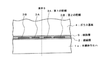
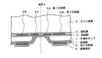
まず、図1に示すように、半導体ウエハ1aを用意する。この半導体ウエハ1aは後述する工程で、切断され複数の半導体チップ1に分離される。それらの半導体チップ1は、例えばCCDのイメージセンサや半導体メモリのチップであり、半導体のウエハプロセスにより形成される。その半導体ウエハ1aの表面に絶縁膜2を介して、複数の第1の配線3A、複数の第2の配線3Bを同時に形成する。第1の配線3Aは、半導体ウエハ1aを複数の半導体チップ1に切断分離するための境界Sを挟んで、その両側に所定の間隙を有して形成される。境界Sは、ダイシングラインまたはスクライブラインと称されるものである。
First, as shown in FIG. 1, a semiconductor wafer 1a is prepared. The semiconductor wafer 1a is cut and separated into a plurality of
ここで、第1の配線3Aは、半導体チップ1の通常のボンディングパッド位置から、境界S付近まで拡張されたパッドである。また、複数の第2の配線3Bは、後の工程で、半導体チップ1上に積層される他の半導体装置の導電端子と電気的に接続される導電パッドである。
Here, the
続いて、第1の配線3A及び第2の配線3Bが形成された半導体ウエハ1aの表面に、支持体であるガラス基板4を、エポキシ樹脂層5を接着剤として用いて接着する。なお、ここでは、支持体としてガラス基板、接着剤としてエポキシ樹脂層を使用しているが、シリコン基板やプラスチックの板の他にテープまたはシート状のものを支持体として用いてもよく、接着剤はこれらの支持体に対して適切な接着材を選択すればよい。
Subsequently, the glass substrate 4 as a support is bonded to the surface of the semiconductor wafer 1a on which the
次に、図2に示すように、前記半導体ウエハ1aのガラス基板4が接着されていない面、即ちその裏面をバックグラインドして、半導体ウエハ1aの厚さを薄く加工する。バックグラインドされた半導体ウエハ1aの裏面は、スクラッチが発生し、幅、深さが数μm程度になる凹凸ができる。これを小さくするために、絶縁膜2の材料であるシリコン酸化膜(以下SiO2)よりも半導体ウエハ1aの材料であるシリコン(以下Si)に対して高い選択比を持つシリコンエッチング液を用いてウェットエッチングを行う。そのようなシリコンエッチング液としては、例えば、フッ化水素酸2.5%、硝酸50%、酢酸10%及び水37.5%の混合溶液が適している。
Next, as shown in FIG. 2, the surface of the semiconductor wafer 1a to which the glass substrate 4 is not bonded, that is, the back surface thereof is back-ground to reduce the thickness of the semiconductor wafer 1a. On the back surface of the back-ground semiconductor wafer 1a, scratches are generated, and irregularities having a width and a depth of about several μm are formed. To reduce this, by using a silicon etching solution with a high selectivity with respect to silicon (hereinafter Si) which is the material of the semiconductor wafer 1a than the silicon oxide film (hereinafter SiO 2) which is a material of the
次に、図3に示すように、前記半導体ウエハ1aの裏面に対して、境界Sに沿って開口部を設けた不図示のレジストパターンをマスクとして、等方性のエッチングを行う。これにより、境界Sの部分で溝が形成され、絶縁膜2が部分的に露出した状態となる。なお、このエッチングは、ドライエッチング、ウェットエッチングのどちらで行ってもよい。このエッチングにより、半導体ウエハ1aは複数の半導体チップ1に切断されるが、ガラス基板4によって支持され、半導体ウエハ1aの形態を維持している。
Next, as shown in FIG. 3, isotropic etching is performed on the back surface of the semiconductor wafer 1a using a resist pattern (not shown) provided with openings along the boundary S as a mask. Thereby, a groove is formed at the boundary S, and the
エッチングされた半導体ウエハ1aの裏面には、凹凸、残渣、異物が存在し、また、図3中の破線円a、bで示されたような角部が形成される。そこで、図4に示すように、残渣や異物を除去し、さらに角部を丸めるためにウェットエッチングを行う。これにより、図3の破線円a、bで示されるような角部は、図4で破線円a、bで示されるように滑らかな形状になる。 On the back surface of the etched semiconductor wafer 1a, there are irregularities, residues, and foreign matters, and corners as shown by broken circles a and b in FIG. 3 are formed. Therefore, as shown in FIG. 4, wet etching is performed to remove residues and foreign matters and further round the corners. Thereby, the corners as shown by the broken circles a and b in FIG. 3 have a smooth shape as shown by the broken circles a and b in FIG.
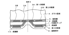
次に、図5に示すように、複数の半導体チップ1の裏面及び、それらのエッチングされた側面に絶縁膜7を被着する。絶縁膜7は例えばシランベースの酸化膜である。
Next, as shown in FIG. 5, an insulating film 7 is deposited on the back surfaces of the plurality of
次に、図6に示すように、半導体チップの裏面に不図示のレジストを塗布し、パターニングを行う。そのレジスト膜をマスクにして、絶縁膜7、絶縁膜2をエッチングし、第1の配線3Aの端部を露出させる。
Next, as shown in FIG. 6, a resist (not shown) is applied to the back surface of the semiconductor chip and patterned. Using the resist film as a mask, the insulating film 7 and the
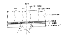
次に、後に導電端子11を形成する位置と重なる位置に柔軟性を有する緩衝部材8を形成する。なお、緩衝部材8は導電端子11に加わる力を吸収し、導電端子11の接合時のストレスを緩和する機能を持つものであるが、必ずしも必要ではない。次に、絶縁膜7、緩衝部材8、第1の配線3Aの露出部分を被う第3の配線9を形成する。これにより、第1の配線3Aと第3の配線9とは電気的に接続される。
Next, the buffer member 8 having flexibility is formed at a position overlapping with a position where the conductive terminal 11 is formed later. Although the buffer member 8 has a function of absorbing a force applied to the conductive terminal 11 and relieving stress at the time of joining the conductive terminal 11, it is not always necessary. Next, a third wiring 9 that covers the insulating film 7, the buffer member 8, and the exposed portion of the
次に図7に示すように、半導体チップ1の裏面側に、不図示のレジストを塗布し、このレジストの境界Sに沿う部分を開口させるようにパターン形成を行う。そして、そのレジストをマスクとしてエッチングを行い、境界S付近の第3の配線9を除去する。なお、不図示であるが、第3の配線9の形成後、無電解メッキ処理を行い、第3の配線9の表面にNi−Auのメッキを施してもよい。
Next, as shown in FIG. 7, a resist (not shown) is applied to the back side of the
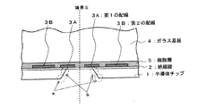
次に、半導体チップ1の裏面側に保護膜10を形成する。保護膜10を形成するためには、半導体チップ1の裏面側を上に向けて、熱硬化性の有機系樹脂を上方から滴下して、複数の半導体チップ1を有し、ガラス基板4が接着された半導体ウエハ1aを回転させる。この回転により生じる遠心力により、有機系樹脂は半導体ウエハ1aの面上に広がる。これにより、第3の配線9の表面に保護膜10を形成することができる。
Next, the protective film 10 is formed on the back surface side of the
次に、図8に示すように、導電端子11を形成する部分の保護膜10を、レジストマスクを利用したエッチングにより選択的に除去して、第3の配線9を露出させ、この露出された第3の配線9上に接触する導電端子11を形成する。導電端子11は、例えば、はんだバンプや金バンプのような突起電極端子で形成することができる。導電端子11の厚さは、はんだバンプを用いる場合は160μmであるが、金バンプを用いる場合には数μm〜数十μmに減少させることができる。導電端子11は、半導体チップ1の裏面に同様な構造で、複数個設け、ボールグリッドアレイ(Ball Grid Array)を構成することができる。
Next, as shown in FIG. 8, the portion of the protective film 10 where the conductive terminal 11 is to be formed is selectively removed by etching using a resist mask to expose the third wiring 9, which is exposed. A conductive terminal 11 is formed on the third wiring 9 in contact therewith. The conductive terminal 11 can be formed of a protruding electrode terminal such as a solder bump or a gold bump, for example. The thickness of the conductive terminal 11 is 160 μm when using solder bumps, but can be reduced to several μm to several tens of μm when using gold bumps. A plurality of conductive terminals 11 having the same structure on the back surface of the
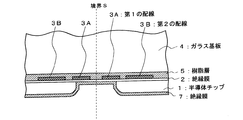
次に、ガラス基板4の表面を削ることにより、その厚さを薄くする。これにより、後述するガラス基板4に開口部を形成するための加工時間を短縮することができる。ガラス基板の厚さは、50μmから100μmが適当である。ガラス基板4を薄くする方法としては、(1)バックグラインド装置でガラス基板4を研削する方法、(2)CMP装置でガラス基板4を研磨する方法、(3)レジスト塗布の様に、ガラス基板4上にエッチング液を滴下し、ガラス基板4が接着された半導体ウエハ1aを回転させることによりエッチング液をガラス基板4の全体に行き渡らせ、ガラス基板4のエッチングを行う方法、(4)ドライエッチングを用いてガラス基板4をエッチングする方法が挙げられる。なお、本発明では、ガラス基板4を薄くする工程を具備しているが、最初から所定厚みの板材やテープまたはシート状のものから成る支持体の使用を制限するものではない。 Next, the surface of the glass substrate 4 is scraped to reduce its thickness. Thereby, the processing time for forming an opening part in the glass substrate 4 mentioned later can be shortened. The thickness of the glass substrate is suitably 50 μm to 100 μm. As a method of thinning the glass substrate 4, (1) a method of grinding the glass substrate 4 with a back grinding apparatus, (2) a method of polishing the glass substrate 4 with a CMP apparatus, and (3) a glass substrate such as resist coating. A method of etching the glass substrate 4 by dropping the etching solution on the substrate 4 and rotating the semiconductor wafer 1a to which the glass substrate 4 is bonded to spread the etching solution over the entire glass substrate 4; (4) dry etching And a method of etching the glass substrate 4 using the above. In addition, in this invention, although the process which thins the glass substrate 4 is provided, use of the support body which consists of a board | plate material, tape, or a sheet-like thing of predetermined thickness from the beginning is not restrict | limited.
次に、図10に示すように、第2の配線3Bの一部上のガラス基板4と樹脂層5をエッチング等により除去し、第2の配線3Bの表面を露出する開口部12を形成する。なお、逆に開口部12を形成した後に、ガラス基板4を削って薄くしてもよいが、開口部12を形成するための加工時間が長くなる。 次に、開口部12によって露出された第2の配線3Bの表面にめっき層13を形成する。めっき層13は、第2の配線3Bの一部を構成する。めっき層13は例えば、Niめっき層とAuめっき層を積層して形成される。
Next, as shown in FIG. 10, the glass substrate 4 and the resin layer 5 on a part of the
次に、図12に示すように、ダイシング装置を用いて、境界Sに沿って半導体ウエハ1aを切断し、複数の半導体チップ1に分離する。このとき、境界Sに沿ってガラス基板4、樹脂層5、保護膜10が切断されることになる。これにより、半導体チップ1aを組み込んだBGA型の半導体装置100が完成する。このBGA型の半導体装置100によれば、半導体チップ1を支持するガラス基板4を一枚だけ半導体チップ1に接着し、かつそのガラス基板4を薄く加工しているのでパッケージ全体を薄くすることができる。また、ガラス基板4には、半導体チップ1の第2の配線3Bを露出する開口部12を形成しているので、この開口部12を通して、外部の電子回路との必要な電気的接続を得ることができる。
Next, as shown in FIG. 12, the semiconductor wafer 1 a is cut along the boundary S and separated into a plurality of
図13は、そのような電気的接続構造の一例として、積層型MCMの構造を示す断面図である。この積層型MCMでは、第1の半導体装置100aと第2の半導体装置100bを積層したものである。第1の半導体装置100aと第2の半導体装置100bは、上述した半導体装置100と同様な構造を有している。第1の半導体装置100aの第2の配線3Bには、開口部12を通して、第2の半導体装置100Bの導電端子11Bが電気的及び機械的に接続されている。その接続強度が不足する場合は、アンダーフィルなどの有機系の接着剤を補助的に用いてもよい。また、積層する半導体装置の数は、必要に応じて選択することができる。
FIG. 13 is a cross-sectional view showing the structure of a stacked MCM as an example of such an electrical connection structure. In this stacked MCM, a
Claims (9)
前記第1の半導体装置は、第1の半導体チップ上に第1の絶縁膜を介して形成された第1の配線及び第2の配線と、
前記第1及び第2の配線が形成された前記第1の半導体チップ上に接着剤を介して接着され前記第2の配線を露出する開口部を有する支持基板と、
前記第1の半導体チップの側面部及び裏面部に形成された第2の絶縁膜と、
前記第1の配線の裏面に接続され、前記第2の絶縁膜に接するようにして前記半導体チップの側面部から裏面部に延在する第3の配線と、
前記第3の配線を被覆するように半導体チップの裏面部に形成された保護膜と、
前記保護膜を介して前記第3の配線上に形成された導電端子とを備え、
前記第2の半導体装置は、第2の半導体チップと、この第2の半導体チップの裏面に形成された導電端子と、を備え、前記第2の半導体装置の前記導電端子が前記第1の半導体装置の開口部を介して前記第2の配線に接続されていることを特徴とする半導体装置。 A first semiconductor device, and a second semiconductor device disposed on the first semiconductor device,
The first semiconductor device includes a first wiring and a second wiring formed on a first semiconductor chip via a first insulating film,
A support substrate having an opening that is bonded to the first semiconductor chip on which the first and second wirings are formed via an adhesive and exposes the second wiring;
A second insulating film formed on a side surface and a back surface of the first semiconductor chip;
A third wiring connected to the back surface of the first wiring and extending from the side surface portion of the semiconductor chip to the back surface portion so as to be in contact with the second insulating film;
A protective film formed on the back surface of the semiconductor chip so as to cover the third wiring;
A conductive terminal formed on the third wiring via the protective film,
The second semiconductor device includes a second semiconductor chip and a conductive terminal formed on a back surface of the second semiconductor chip, and the conductive terminal of the second semiconductor device is the first semiconductor. A semiconductor device, wherein the semiconductor device is connected to the second wiring through an opening of the device.
前記第1及び第2の配線が形成された前記半導体ウエハ上に接着剤を介して支持基板を接着する工程と、
前記半導体ウエハ裏面から前記複数の半導体チップの境界部分をエッチングする工程と、
前記エッチングにより露出した半導体チップの側面部及び裏面部上に第2の絶縁膜を形成する工程と、
前記第1の配線の裏面に接続され、前記第2の絶縁膜に接するように前記半導体チップの側面部から裏面部に延在する第3の配線を形成する工程と、
前記第3の配線を被覆するように半導体チップの裏面部に保護膜を形成する工程と、
前記保護膜を介して前記第3の配線上に導電端子を形成する工程と、
前記支持基板に前記第2の配線を露出する開口部を形成する工程と、
前記境界部分に沿って複数の半導体チップに分断する工程とを具備し、
前記分断された第1の半導体チップの開口部を介して露出した第2の配線に第2の半導体チップの導電端子を接続することで、第1の半導体チップ上に第2の半導体チップを積層することを特徴とする半導体装置の製造方法。 Preparing a semiconductor wafer having a plurality of semiconductor chips on which a first wiring and a second wiring are formed via a first insulating film;
Bonding a support substrate on the semiconductor wafer on which the first and second wirings are formed via an adhesive;
Etching a boundary portion of the plurality of semiconductor chips from the back surface of the semiconductor wafer;
Forming a second insulating film on the side and back surfaces of the semiconductor chip exposed by the etching;
Forming a third wiring connected to the back surface of the first wiring and extending from the side surface of the semiconductor chip to the back surface so as to be in contact with the second insulating film;
Forming a protective film on the back surface of the semiconductor chip so as to cover the third wiring;
Forming a conductive terminal on the third wiring through the protective film;
Forming an opening exposing the second wiring on the support substrate;
Dividing the plurality of semiconductor chips along the boundary portion,
The second semiconductor chip is stacked on the first semiconductor chip by connecting the conductive terminal of the second semiconductor chip to the second wiring exposed through the opening of the divided first semiconductor chip. A method of manufacturing a semiconductor device.
Priority Applications (1)
| Application Number | Priority Date | Filing Date | Title |
|---|---|---|---|
| JP2004114979A JP4334397B2 (en) | 2003-04-24 | 2004-04-09 | Semiconductor device and manufacturing method thereof |
Applications Claiming Priority (2)
| Application Number | Priority Date | Filing Date | Title |
|---|---|---|---|
| JP2003120228 | 2003-04-24 | ||
| JP2004114979A JP4334397B2 (en) | 2003-04-24 | 2004-04-09 | Semiconductor device and manufacturing method thereof |
Publications (2)
| Publication Number | Publication Date |
|---|---|
| JP2004343088A JP2004343088A (en) | 2004-12-02 |
| JP4334397B2 true JP4334397B2 (en) | 2009-09-30 |
Family
ID=33543219
Family Applications (1)
| Application Number | Title | Priority Date | Filing Date |
|---|---|---|---|
| JP2004114979A Expired - Fee Related JP4334397B2 (en) | 2003-04-24 | 2004-04-09 | Semiconductor device and manufacturing method thereof |
Country Status (1)
| Country | Link |
|---|---|
| JP (1) | JP4334397B2 (en) |
Families Citing this family (10)
| Publication number | Priority date | Publication date | Assignee | Title |
|---|---|---|---|---|
| JP2006179709A (en) * | 2004-12-22 | 2006-07-06 | Sanyo Electric Co Ltd | Manufacturing method for semiconductor device |
| TWI313914B (en) * | 2005-01-31 | 2009-08-21 | Sanyo Electric Co | Semiconductor device and a method for manufacturing thereof |
| KR100759309B1 (en) | 2005-08-08 | 2007-09-17 | 세이코 엡슨 가부시키가이샤 | Semiconductor device |
| JP4235835B2 (en) | 2005-08-08 | 2009-03-11 | セイコーエプソン株式会社 | Semiconductor device |
| TW200737506A (en) | 2006-03-07 | 2007-10-01 | Sanyo Electric Co | Semiconductor device and manufacturing method of the same |
| JP5555400B2 (en) * | 2006-08-04 | 2014-07-23 | セミコンダクター・コンポーネンツ・インダストリーズ・リミテッド・ライアビリティ・カンパニー | Semiconductor device and manufacturing method thereof |
| US8018071B2 (en) | 2007-02-07 | 2011-09-13 | Samsung Electronics Co., Ltd. | Stacked structure using semiconductor devices and semiconductor device package including the same |
| JP5122184B2 (en) * | 2007-05-30 | 2013-01-16 | オンセミコンダクター・トレーディング・リミテッド | Semiconductor device and manufacturing method thereof |
| JP5101157B2 (en) * | 2007-05-07 | 2012-12-19 | オンセミコンダクター・トレーディング・リミテッド | Manufacturing method of semiconductor device |
| JP5399542B2 (en) * | 2012-08-08 | 2014-01-29 | 富士通株式会社 | Manufacturing method of semiconductor device |
-
2004
- 2004-04-09 JP JP2004114979A patent/JP4334397B2/en not_active Expired - Fee Related
Also Published As
| Publication number | Publication date |
|---|---|
| JP2004343088A (en) | 2004-12-02 |
Similar Documents
| Publication | Publication Date | Title |
|---|---|---|
| KR100938970B1 (en) | Semiconductor device and manufacturing method thereof | |
| JP4401181B2 (en) | Semiconductor device and manufacturing method thereof | |
| KR100621438B1 (en) | Stack chip package using photo sensitive polymer and manufacturing method thereof | |
| US7981807B2 (en) | Manufacturing method of semiconductor device with smoothing | |
| KR100486832B1 (en) | Semiconductor Chip, Chip Stack Package And Manufacturing Method | |
| KR101245928B1 (en) | Ultra-thin stacked chips packaging | |
| JP4100936B2 (en) | Manufacturing method of semiconductor device | |
| JP2008235401A (en) | Semiconductor device and manufacturing method therefor | |
| JP4093018B2 (en) | Semiconductor device and manufacturing method thereof | |
| JP2003086762A (en) | Semiconductor device and manufacturing method therefor | |
| JP2004165189A (en) | Semiconductor device and method of manufacturing the same | |
| JP4334397B2 (en) | Semiconductor device and manufacturing method thereof | |
| JP2006041512A (en) | Method of manufacturing integrated-circuit chip for multi-chip package, and wafer and chip formed by the method thereof | |
| JP3877700B2 (en) | Semiconductor device and manufacturing method thereof | |
| JP5238985B2 (en) | Manufacturing method of semiconductor device | |
| JP4401330B2 (en) | Semiconductor device and manufacturing method thereof | |
| JP4371719B2 (en) | Semiconductor device and manufacturing method thereof | |
| JP3917121B2 (en) | Manufacturing method of semiconductor device | |
| JP4522213B2 (en) | Manufacturing method of semiconductor device | |
| JP4805362B2 (en) | Manufacturing method of semiconductor device | |
| JP4597182B2 (en) | Semiconductor device and manufacturing method thereof | |
| JP2010087295A (en) | Semiconductor chip and method of manufacturing the same and semiconductor device and method of manufacturing the same | |
| JP2006179709A (en) | Manufacturing method for semiconductor device | |
| JP2005101411A (en) | Semiconductor device and method for manufacturing the same |
Legal Events
| Date | Code | Title | Description |
|---|---|---|---|
| A621 | Written request for application examination |
Free format text: JAPANESE INTERMEDIATE CODE: A621 Effective date: 20070302 |
|
| A977 | Report on retrieval |
Free format text: JAPANESE INTERMEDIATE CODE: A971007 Effective date: 20081128 |
|
| A131 | Notification of reasons for refusal |
Free format text: JAPANESE INTERMEDIATE CODE: A131 Effective date: 20081202 |
|
| A521 | Request for written amendment filed |
Free format text: JAPANESE INTERMEDIATE CODE: A523 Effective date: 20090129 |
|
| A131 | Notification of reasons for refusal |
Free format text: JAPANESE INTERMEDIATE CODE: A131 Effective date: 20090310 |
|
| A521 | Request for written amendment filed |
Free format text: JAPANESE INTERMEDIATE CODE: A523 Effective date: 20090508 |
|
| TRDD | Decision of grant or rejection written | ||
| A01 | Written decision to grant a patent or to grant a registration (utility model) |
Free format text: JAPANESE INTERMEDIATE CODE: A01 Effective date: 20090528 |
|
| A01 | Written decision to grant a patent or to grant a registration (utility model) |
Free format text: JAPANESE INTERMEDIATE CODE: A01 |
|
| A61 | First payment of annual fees (during grant procedure) |
Free format text: JAPANESE INTERMEDIATE CODE: A61 Effective date: 20090623 |
|
| FPAY | Renewal fee payment (event date is renewal date of database) |
Free format text: PAYMENT UNTIL: 20120703 Year of fee payment: 3 |
|
| FPAY | Renewal fee payment (event date is renewal date of database) |
Free format text: PAYMENT UNTIL: 20120703 Year of fee payment: 3 |
|
| FPAY | Renewal fee payment (event date is renewal date of database) |
Free format text: PAYMENT UNTIL: 20130703 Year of fee payment: 4 |
|
| R250 | Receipt of annual fees |
Free format text: JAPANESE INTERMEDIATE CODE: R250 |
|
| LAPS | Cancellation because of no payment of annual fees |