JP4212815B2 - Light emitting device - Google Patents
Light emitting device Download PDFInfo
- Publication number
- JP4212815B2 JP4212815B2 JP2002037621A JP2002037621A JP4212815B2 JP 4212815 B2 JP4212815 B2 JP 4212815B2 JP 2002037621 A JP2002037621 A JP 2002037621A JP 2002037621 A JP2002037621 A JP 2002037621A JP 4212815 B2 JP4212815 B2 JP 4212815B2
- Authority
- JP
- Japan
- Prior art keywords
- transistor
- pixel
- light emitting
- film
- oled
- Prior art date
- Legal status (The legal status is an assumption and is not a legal conclusion. Google has not performed a legal analysis and makes no representation as to the accuracy of the status listed.)
- Expired - Fee Related
Links
- 239000003990 capacitor Substances 0.000 claims description 51
- 239000010408 film Substances 0.000 description 218
- 239000010410 layer Substances 0.000 description 175
- 238000000034 method Methods 0.000 description 79
- 239000011229 interlayer Substances 0.000 description 51
- 239000000463 material Substances 0.000 description 51
- 239000012535 impurity Substances 0.000 description 49
- 239000000758 substrate Substances 0.000 description 42
- 238000003860 storage Methods 0.000 description 33
- 239000004065 semiconductor Substances 0.000 description 30
- 238000010586 diagram Methods 0.000 description 24
- 238000005530 etching Methods 0.000 description 24
- 229910052760 oxygen Inorganic materials 0.000 description 21
- XUIMIQQOPSSXEZ-UHFFFAOYSA-N Silicon Chemical compound [Si] XUIMIQQOPSSXEZ-UHFFFAOYSA-N 0.000 description 19
- 230000001681 protective effect Effects 0.000 description 19
- 229910052710 silicon Inorganic materials 0.000 description 19
- 239000010703 silicon Substances 0.000 description 19
- QVGXLLKOCUKJST-UHFFFAOYSA-N atomic oxygen Chemical compound [O] QVGXLLKOCUKJST-UHFFFAOYSA-N 0.000 description 16
- 239000007789 gas Substances 0.000 description 16
- 239000001301 oxygen Substances 0.000 description 16
- 238000004519 manufacturing process Methods 0.000 description 15
- 239000000126 substance Substances 0.000 description 15
- 238000006243 chemical reaction Methods 0.000 description 11
- 230000008569 process Effects 0.000 description 11
- 238000007740 vapor deposition Methods 0.000 description 11
- 230000008859 change Effects 0.000 description 10
- 238000002347 injection Methods 0.000 description 10
- 239000007924 injection Substances 0.000 description 10
- 229920005989 resin Polymers 0.000 description 10
- 239000011347 resin Substances 0.000 description 10
- VYPSYNLAJGMNEJ-UHFFFAOYSA-N silicon dioxide Inorganic materials O=[Si]=O VYPSYNLAJGMNEJ-UHFFFAOYSA-N 0.000 description 10
- 238000004544 sputter deposition Methods 0.000 description 10
- 229910052814 silicon oxide Inorganic materials 0.000 description 9
- 239000012298 atmosphere Substances 0.000 description 8
- UMIVXZPTRXBADB-UHFFFAOYSA-N benzocyclobutene Chemical compound C1=CC=C2CCC2=C1 UMIVXZPTRXBADB-UHFFFAOYSA-N 0.000 description 8
- 230000007423 decrease Effects 0.000 description 8
- 230000006866 deterioration Effects 0.000 description 8
- 229910052739 hydrogen Inorganic materials 0.000 description 8
- 238000005268 plasma chemical vapour deposition Methods 0.000 description 8
- 239000004642 Polyimide Substances 0.000 description 7
- 229910052581 Si3N4 Inorganic materials 0.000 description 7
- XLOMVQKBTHCTTD-UHFFFAOYSA-N Zinc monoxide Chemical compound [Zn]=O XLOMVQKBTHCTTD-UHFFFAOYSA-N 0.000 description 7
- NIXOWILDQLNWCW-UHFFFAOYSA-N acrylic acid group Chemical group C(C=C)(=O)O NIXOWILDQLNWCW-UHFFFAOYSA-N 0.000 description 7
- 229910045601 alloy Inorganic materials 0.000 description 7
- 239000000956 alloy Substances 0.000 description 7
- 239000002585 base Substances 0.000 description 7
- 230000015572 biosynthetic process Effects 0.000 description 7
- 238000007733 ion plating Methods 0.000 description 7
- 229910052751 metal Inorganic materials 0.000 description 7
- 239000002184 metal Substances 0.000 description 7
- 229920001721 polyimide Polymers 0.000 description 7
- 238000005070 sampling Methods 0.000 description 7
- HQVNEWCFYHHQES-UHFFFAOYSA-N silicon nitride Chemical compound N12[Si]34N5[Si]62N3[Si]51N64 HQVNEWCFYHHQES-UHFFFAOYSA-N 0.000 description 7
- IJGRMHOSHXDMSA-UHFFFAOYSA-N Atomic nitrogen Chemical compound N#N IJGRMHOSHXDMSA-UHFFFAOYSA-N 0.000 description 6
- 229910052782 aluminium Inorganic materials 0.000 description 6
- 238000002425 crystallisation Methods 0.000 description 6
- 238000001704 evaporation Methods 0.000 description 6
- 239000011521 glass Substances 0.000 description 6
- 229910003437 indium oxide Inorganic materials 0.000 description 6
- PJXISJQVUVHSOJ-UHFFFAOYSA-N indium(iii) oxide Chemical compound [O-2].[O-2].[O-2].[In+3].[In+3] PJXISJQVUVHSOJ-UHFFFAOYSA-N 0.000 description 6
- 229910052757 nitrogen Inorganic materials 0.000 description 6
- 238000000151 deposition Methods 0.000 description 5
- 238000002161 passivation Methods 0.000 description 5
- 239000012071 phase Substances 0.000 description 5
- 229920003023 plastic Polymers 0.000 description 5
- 239000004033 plastic Substances 0.000 description 5
- 238000009751 slip forming Methods 0.000 description 5
- XKRFYHLGVUSROY-UHFFFAOYSA-N Argon Chemical compound [Ar] XKRFYHLGVUSROY-UHFFFAOYSA-N 0.000 description 4
- UFHFLCQGNIYNRP-UHFFFAOYSA-N Hydrogen Chemical compound [H][H] UFHFLCQGNIYNRP-UHFFFAOYSA-N 0.000 description 4
- PXHVJJICTQNCMI-UHFFFAOYSA-N Nickel Chemical compound [Ni] PXHVJJICTQNCMI-UHFFFAOYSA-N 0.000 description 4
- OAICVXFJPJFONN-UHFFFAOYSA-N Phosphorus Chemical compound [P] OAICVXFJPJFONN-UHFFFAOYSA-N 0.000 description 4
- 239000004952 Polyamide Substances 0.000 description 4
- XAGFODPZIPBFFR-UHFFFAOYSA-N aluminium Chemical compound [Al] XAGFODPZIPBFFR-UHFFFAOYSA-N 0.000 description 4
- 229910021417 amorphous silicon Inorganic materials 0.000 description 4
- 238000000137 annealing Methods 0.000 description 4
- 230000008025 crystallization Effects 0.000 description 4
- 230000008021 deposition Effects 0.000 description 4
- 239000000945 filler Substances 0.000 description 4
- 238000010438 heat treatment Methods 0.000 description 4
- 230000005525 hole transport Effects 0.000 description 4
- 239000001257 hydrogen Substances 0.000 description 4
- 239000011810 insulating material Substances 0.000 description 4
- 150000002500 ions Chemical class 0.000 description 4
- 150000002894 organic compounds Chemical class 0.000 description 4
- 229910052698 phosphorus Inorganic materials 0.000 description 4
- 239000011574 phosphorus Substances 0.000 description 4
- 229920002647 polyamide Polymers 0.000 description 4
- 239000000565 sealant Substances 0.000 description 4
- 239000003566 sealing material Substances 0.000 description 4
- 239000002356 single layer Substances 0.000 description 4
- BOTDANWDWHJENH-UHFFFAOYSA-N Tetraethyl orthosilicate Chemical compound CCO[Si](OCC)(OCC)OCC BOTDANWDWHJENH-UHFFFAOYSA-N 0.000 description 3
- 230000001133 acceleration Effects 0.000 description 3
- 230000006870 function Effects 0.000 description 3
- AMGQUBHHOARCQH-UHFFFAOYSA-N indium;oxotin Chemical compound [In].[Sn]=O AMGQUBHHOARCQH-UHFFFAOYSA-N 0.000 description 3
- 239000004973 liquid crystal related substance Substances 0.000 description 3
- 239000000203 mixture Substances 0.000 description 3
- 230000010355 oscillation Effects 0.000 description 3
- 229920002620 polyvinyl fluoride Polymers 0.000 description 3
- 229910052719 titanium Inorganic materials 0.000 description 3
- 150000005072 1,3,4-oxadiazoles Chemical class 0.000 description 2
- 229920002799 BoPET Polymers 0.000 description 2
- RYGMFSIKBFXOCR-UHFFFAOYSA-N Copper Chemical compound [Cu] RYGMFSIKBFXOCR-UHFFFAOYSA-N 0.000 description 2
- 239000005041 Mylar™ Substances 0.000 description 2
- 229910052786 argon Inorganic materials 0.000 description 2
- QVQLCTNNEUAWMS-UHFFFAOYSA-N barium oxide Chemical compound [Ba]=O QVQLCTNNEUAWMS-UHFFFAOYSA-N 0.000 description 2
- DQXBYHZEEUGOBF-UHFFFAOYSA-N but-3-enoic acid;ethene Chemical compound C=C.OC(=O)CC=C DQXBYHZEEUGOBF-UHFFFAOYSA-N 0.000 description 2
- 150000001875 compounds Chemical class 0.000 description 2
- 239000011231 conductive filler Substances 0.000 description 2
- 229920001940 conductive polymer Polymers 0.000 description 2
- 229910052802 copper Inorganic materials 0.000 description 2
- 239000010949 copper Substances 0.000 description 2
- ZYGHJZDHTFUPRJ-UHFFFAOYSA-N coumarin Chemical compound C1=CC=C2OC(=O)C=CC2=C1 ZYGHJZDHTFUPRJ-UHFFFAOYSA-N 0.000 description 2
- VBVAVBCYMYWNOU-UHFFFAOYSA-N coumarin 6 Chemical compound C1=CC=C2SC(C3=CC4=CC=C(C=C4OC3=O)N(CC)CC)=NC2=C1 VBVAVBCYMYWNOU-UHFFFAOYSA-N 0.000 description 2
- 239000013078 crystal Substances 0.000 description 2
- 229910021419 crystalline silicon Inorganic materials 0.000 description 2
- 238000007599 discharging Methods 0.000 description 2
- 238000001312 dry etching Methods 0.000 description 2
- 239000005038 ethylene vinyl acetate Substances 0.000 description 2
- 230000008020 evaporation Effects 0.000 description 2
- 230000005284 excitation Effects 0.000 description 2
- 230000005281 excited state Effects 0.000 description 2
- 239000011152 fibreglass Substances 0.000 description 2
- 230000005283 ground state Effects 0.000 description 2
- 238000005984 hydrogenation reaction Methods 0.000 description 2
- 239000011261 inert gas Substances 0.000 description 2
- 238000005224 laser annealing Methods 0.000 description 2
- 238000005499 laser crystallization Methods 0.000 description 2
- 238000004020 luminiscence type Methods 0.000 description 2
- 239000007769 metal material Substances 0.000 description 2
- 229910052759 nickel Inorganic materials 0.000 description 2
- 238000000059 patterning Methods 0.000 description 2
- 238000000206 photolithography Methods 0.000 description 2
- 229920003227 poly(N-vinyl carbazole) Polymers 0.000 description 2
- 229920001200 poly(ethylene-vinyl acetate) Polymers 0.000 description 2
- 229920000553 poly(phenylenevinylene) Polymers 0.000 description 2
- 229920002037 poly(vinyl butyral) polymer Polymers 0.000 description 2
- 229920006267 polyester film Polymers 0.000 description 2
- -1 polyphenylene vinylene Polymers 0.000 description 2
- 229920000915 polyvinyl chloride Polymers 0.000 description 2
- 239000004800 polyvinyl chloride Substances 0.000 description 2
- XOLBLPGZBRYERU-UHFFFAOYSA-N tin dioxide Chemical compound O=[Sn]=O XOLBLPGZBRYERU-UHFFFAOYSA-N 0.000 description 2
- 229910001887 tin oxide Inorganic materials 0.000 description 2
- 238000001771 vacuum deposition Methods 0.000 description 2
- 239000011787 zinc oxide Substances 0.000 description 2
- 239000004925 Acrylic resin Substances 0.000 description 1
- 229920000178 Acrylic resin Polymers 0.000 description 1
- ZOXJGFHDIHLPTG-UHFFFAOYSA-N Boron Chemical compound [B] ZOXJGFHDIHLPTG-UHFFFAOYSA-N 0.000 description 1
- GYHNNYVSQQEPJS-UHFFFAOYSA-N Gallium Chemical compound [Ga] GYHNNYVSQQEPJS-UHFFFAOYSA-N 0.000 description 1
- 229910000577 Silicon-germanium Inorganic materials 0.000 description 1
- BQCADISMDOOEFD-UHFFFAOYSA-N Silver Chemical compound [Ag] BQCADISMDOOEFD-UHFFFAOYSA-N 0.000 description 1
- LEVVHYCKPQWKOP-UHFFFAOYSA-N [Si].[Ge] Chemical compound [Si].[Ge] LEVVHYCKPQWKOP-UHFFFAOYSA-N 0.000 description 1
- 230000003213 activating effect Effects 0.000 description 1
- 230000004913 activation Effects 0.000 description 1
- 229910052783 alkali metal Inorganic materials 0.000 description 1
- 150000001340 alkali metals Chemical class 0.000 description 1
- 239000005407 aluminoborosilicate glass Substances 0.000 description 1
- 150000001408 amides Chemical class 0.000 description 1
- 229910052785 arsenic Inorganic materials 0.000 description 1
- RQNWIZPPADIBDY-UHFFFAOYSA-N arsenic atom Chemical compound [As] RQNWIZPPADIBDY-UHFFFAOYSA-N 0.000 description 1
- 229910052788 barium Inorganic materials 0.000 description 1
- DSAJWYNOEDNPEQ-UHFFFAOYSA-N barium atom Chemical compound [Ba] DSAJWYNOEDNPEQ-UHFFFAOYSA-N 0.000 description 1
- 230000005540 biological transmission Effects 0.000 description 1
- 229910052796 boron Inorganic materials 0.000 description 1
- 239000005388 borosilicate glass Substances 0.000 description 1
- 238000009125 cardiac resynchronization therapy Methods 0.000 description 1
- 230000015556 catabolic process Effects 0.000 description 1
- 239000003054 catalyst Substances 0.000 description 1
- 230000001413 cellular effect Effects 0.000 description 1
- 229910010293 ceramic material Inorganic materials 0.000 description 1
- 239000003795 chemical substances by application Substances 0.000 description 1
- 238000005229 chemical vapour deposition Methods 0.000 description 1
- 239000011248 coating agent Substances 0.000 description 1
- 238000000576 coating method Methods 0.000 description 1
- 238000004891 communication Methods 0.000 description 1
- 229960000956 coumarin Drugs 0.000 description 1
- 235000001671 coumarin Nutrition 0.000 description 1
- 238000005336 cracking Methods 0.000 description 1
- 230000007547 defect Effects 0.000 description 1
- 238000006731 degradation reaction Methods 0.000 description 1
- ZOCHARZZJNPSEU-UHFFFAOYSA-N diboron Chemical compound B#B ZOCHARZZJNPSEU-UHFFFAOYSA-N 0.000 description 1
- 230000000694 effects Effects 0.000 description 1
- 230000005684 electric field Effects 0.000 description 1
- 239000007772 electrode material Substances 0.000 description 1
- 239000003822 epoxy resin Substances 0.000 description 1
- 239000011888 foil Substances 0.000 description 1
- 229910052733 gallium Inorganic materials 0.000 description 1
- 239000002784 hot electron Substances 0.000 description 1
- 229910010272 inorganic material Inorganic materials 0.000 description 1
- 239000011147 inorganic material Substances 0.000 description 1
- 230000001678 irradiating effect Effects 0.000 description 1
- 238000004518 low pressure chemical vapour deposition Methods 0.000 description 1
- 239000011159 matrix material Substances 0.000 description 1
- 238000002156 mixing Methods 0.000 description 1
- 229910021421 monocrystalline silicon Inorganic materials 0.000 description 1
- 239000000178 monomer Substances 0.000 description 1
- 239000012299 nitrogen atmosphere Substances 0.000 description 1
- 230000003287 optical effect Effects 0.000 description 1
- 239000011368 organic material Substances 0.000 description 1
- 230000003647 oxidation Effects 0.000 description 1
- 238000007254 oxidation reaction Methods 0.000 description 1
- 230000003071 parasitic effect Effects 0.000 description 1
- 238000009832 plasma treatment Methods 0.000 description 1
- 239000002985 plastic film Substances 0.000 description 1
- 229920006255 plastic film Polymers 0.000 description 1
- 229910021420 polycrystalline silicon Inorganic materials 0.000 description 1
- 229920000647 polyepoxide Polymers 0.000 description 1
- 229920000642 polymer Polymers 0.000 description 1
- 238000003825 pressing Methods 0.000 description 1
- 239000010453 quartz Substances 0.000 description 1
- 238000004151 rapid thermal annealing Methods 0.000 description 1
- 230000004044 response Effects 0.000 description 1
- 230000000717 retained effect Effects 0.000 description 1
- 238000007789 sealing Methods 0.000 description 1
- SBEQWOXEGHQIMW-UHFFFAOYSA-N silicon Chemical group [Si].[Si] SBEQWOXEGHQIMW-UHFFFAOYSA-N 0.000 description 1
- 229920002050 silicone resin Polymers 0.000 description 1
- 229910052709 silver Inorganic materials 0.000 description 1
- 239000004332 silver Substances 0.000 description 1
- 239000000243 solution Substances 0.000 description 1
- 239000010935 stainless steel Substances 0.000 description 1
- 229910001220 stainless steel Inorganic materials 0.000 description 1
- 238000004381 surface treatment Methods 0.000 description 1
- 229910052715 tantalum Inorganic materials 0.000 description 1
- 238000002230 thermal chemical vapour deposition Methods 0.000 description 1
- 229920001187 thermosetting polymer Polymers 0.000 description 1
- 239000010409 thin film Substances 0.000 description 1
- 239000012780 transparent material Substances 0.000 description 1
- 229910052721 tungsten Inorganic materials 0.000 description 1
- NXHILIPIEUBEPD-UHFFFAOYSA-H tungsten hexafluoride Chemical compound F[W](F)(F)(F)(F)F NXHILIPIEUBEPD-UHFFFAOYSA-H 0.000 description 1
- 239000012808 vapor phase Substances 0.000 description 1
- 238000001039 wet etching Methods 0.000 description 1
Images


Landscapes
- Electroluminescent Light Sources (AREA)
- Control Of Indicators Other Than Cathode Ray Tubes (AREA)
- Control Of El Displays (AREA)
- Thin Film Transistor (AREA)
Description
【0001】
【発明の属する技術分野】
本発明は、基板上に形成された有機OLED(OLED:Organic Light Emitting Device)を、該基板とカバー材の間に封入したOLEDパネルに関する。また、該OLEDパネルにコントローラを含むIC等を実装した、OLEDモジュールに関する。なお本明細書において、OLEDパネル及びOLEDモジュールを共に発光装置と総称する。本発明はさらに、該発光装置を用いた電子機器に関する。
【0002】
【従来の技術】
OLEDは自ら発光するため視認性が高く、液晶表示装置(LCD)で必要なバックライトが要らず薄型化に最適であると共に、視野角にも制限が無い。そのため、近年OLEDを用いた発光装置は、CRTやLCDに代わる表示装置として注目されている。
【0003】
OLEDは、電場を加えることで発生するルミネッセンス(Electroluminescence)が得られる有機化合物(有機発光材料)を含む層(以下、有機発光層と記す)と、陽極層と、陰極層とを有している。有機化合物におけるルミネッセンスには、一重項励起状態から基底状態に戻る際の発光(蛍光)と三重項励起状態から基底状態に戻る際の発光(リン光)とがあるが、本発明の発光装置は、上述した発光のうちの、いずれか一方の発光を用いていても良いし、または両方の発光を用いていても良い。
【0004】
なお、本明細書では、OLEDの陽極と陰極の間に設けられた全ての層を有機発光層と定義する。有機発光層には具体的に、発光層、正孔注入層、電子注入層、正孔輸送層、電子輸送層等が含まれる。基本的にOLEDは、陽極/発光層/陰極が順に積層された構造を有しており、この構造に加えて、陽極/正孔注入層/発光層/陰極や、陽極/正孔注入層/発光層/電子輸送層/陰極等の順に積層した構造を有していることもある。
【0005】
【発明が解決しようとする課題】
発光装置を実用化する上で問題となっているのが、有機発光材料の劣化に伴う、OLEDの輝度の低下であった。
【0006】
有機発光材料は水分、酸素、光、熱に弱く、これらのものによって劣化が促進される。具体的には、発光装置を駆動するデバイスの構造、有機発光材料の特性、電極の材料、作製工程における条件、発光装置の駆動方法等により、その劣化の速度が左右される。
【0007】
有機発光層にかかる電圧が一定であっても、有機発光層が劣化するとOLEDの輝度は低下し、表示する画像は不鮮明になる。なお本明細書において、一対の電極から有機発光層に印加する電圧をOLED駆動電圧(Vel)と定義する。
【0008】
また、R(赤)、G(緑)、B(青)に対応した三種類のOLEDを用いたカラー化表示方式において、有機発光層を構成する有機発光材料は、OLEDの対応する色によって異なる。そのため、OLEDの有機発光層が、対応する色にごとに異なる速度で劣化することがある。この場合、時間が経つにつれ、OLEDの輝度が色ごとに異なってしまい、発光装置に所望の色を有する画像を表示することができなくなる。
【0009】
また、有機発光層の温度は、外気温やOLEDパネル自身が発する熱等に左右されるが、一般的にOLEDは温度によって流れる電流の値が変化する。図26に、有機発光層の温度を変化させたときの、OLEDの電圧電流特性の変化を示す。電圧が一定のとき、有機発光層の温度が高くなると、OLED駆動電流は大きくなる。そしてOLED駆動電流とOLEDの輝度は比例関係にあるため、OLED駆動電流が大きければ大きいほど、OLEDの輝度は高くなる。このように、有機発光層の温度によってOLEDの輝度が変化するため、所望の階調を表示することが難しく、温度の上昇に伴って発光装置の消費電流が大きくなる。
【0010】
さらに、一般的に、有機発光材料の種類によって温度変化におけるOLED駆動電流の変化の度合いが異なるため、カラー表示において各色のOLEDの輝度が温度によってバラバラに変化することが起こりうる。各色の輝度のバランスが崩れると、所望の色を表示することができない。
【0011】
本発明は上述したことに鑑み、有機発光層の劣化や温度変化に左右されずに一定の輝度を得ることができ、さらに所望のカラー表示を行うことが可能な発光装置を提供することを課題とする。
【0012】
【課題を解決するための手段】
本発明者は、OLED駆動電圧を一定に保って発光させるのと、OLEDに流れる電流を一定に保って発光させるのとでは、後者の方が、劣化によるOLEDの輝度の低下が小さいことに着目した。なお本明細書において、OLEDに流れる電流をOLED駆動電流(Iel)と呼ぶ。そして、OLEDの輝度を電圧によって制御するのではなく、電流によって制御することで、OLEDの劣化によるOLEDの輝度の変化を防ぐことができるのではないかと考えた。
【0013】
具体的に本発明では、トランジスタを用いて形成されたカレントミラー回路を各画素に設ける。そして該カレントミラー回路を用いて、OLED駆動電流を制御する。そして、該カレントミラー回路が有する第1のトランジスタと第2のトランジスタは、負荷抵抗の値によらず、そのドレイン電流がほぼ等しい値に保たれるように接続されている。
【0014】
第1のトランジスタは、そのドレイン電流I1が信号線駆動回路において制御されている。第1のトランジスタのドレイン電流I1の大きさはは、負荷抵抗の値によらず第2のトランジスタのドレイン電流I2の大きさと常に等しくなるので、結果的に第2のトランジスタのドレイン電流I2は信号線駆動回路において制御されることになる。
【0015】
そして、第2のトランジスタは、そのドレイン電流I2がOLEDに流れるように接続される。したがって、OLEDに流れるOLED駆動電流の値は、負荷抵抗の値によらず、信号線駆動回路によって制御される。言い換えると、トランジスタの特性の違いや、OLEDの劣化等に左右されずに、OLED駆動電流を所望の値に制御することが可能になる。
【0016】
本発明では、上記構成により、有機発光層が劣化してもOLEDの輝度の低下を抑えることができ、その結果鮮明な画像を表示することができる。また、各色毎に対応したOLEDを用いたカラー表示の発光装置の場合、OLEDの有機発光層が、対応する色にごとに異なる速度で劣化しても、各色の輝度のバランスが崩れるのを防いで所望の色を表示することができる。
【0017】
また、有機発光層の温度が外気温やOLEDパネル自身が発する熱等に左右されても、OLED駆動電流を所望の値に制御することができる。よって、OLED駆動電流とOLEDの輝度は比例するので、OLEDの輝度が変化するのを抑えることができ、また温度の上昇に伴って消費電流が大きくなるのを防ぐことができる。また、カラー表示の発光装置の場合、温度変化に左右されずに各色のOLEDの輝度の変化を抑えることができるので、各色の輝度のバランスが崩れるのを防ぐことができ、所望の色を表示することができる。
【0018】
さらに、一般的に、有機発光材料の種類によって温度変化におけるOLED駆動電流の変化の度合いが異なるため、カラー表示において各色のOLEDの輝度が温度によってバラバラに変化することが起こりうる。しかし本発明の発光装置では、温度変化に左右されずに所望の輝度を得ることができるので、各色の輝度のバランスが崩れるのを防ぐことができ、所望の色を表示することができる。
【0019】
また一般的な発光装置は、各画素に電流を供給する配線自体が抵抗を有するため、配線の長さによってその電位が多少降下する。そしてこの電位の降下は、表示する画像によっても大きく異なる。特に、同じ配線から電流が供給される複数の画素において、階調数の高い画素の割合が大きくなると、配線に流れる電流が大きくなり、電位の降下が顕著に現れる。電位が降下すると、各画素のOLEDにそれぞれかかる電圧が小さくなるため、各画素に供給される電流は小さくなる。よって、ある所定の画素において一定の階調を表示しようとしても、同じ配線から電流が供給されている他の画素の階調数が変化すると、それに伴って該所定の画素に供給される電流が変化し、結果的に階調数も変化する。しかし本発明の発光装置では、表示する画像毎に測定値と基準値を得て、OLED電流を補正することができるので、表示する画像が変化しても補正により所望の階調数を表示することができる。
【0020】
なお、本発明の発光装置では、画素に用いるトランジスタは単結晶シリコンを用いて形成されたトランジスタであっても良いし、多結晶シリコンやアモルファスシリコンを用いた薄膜トランジスタであっても良い。
【0021】
【発明の実施の形態】
(実施の形態1)
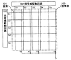
図1に本発明のOLEDパネルの構成を、ブロック図で示す。100は画素部であり、複数の画素101がマトリクス状に形成されている。また102は信号線駆動回路、103は走査線駆動回路である。
【0022】
なお図1では信号線駆動回路102と走査線駆動回路103が、画素部100と同じ基板上に形成されているが、本発明はこの構成に限定されない。信号線駆動回路102と走査線駆動回路103とが画素部100と異なる基板上に形成され、FPC等のコネクターを介して、画素部100と接続されていても良い。また、図1では信号線駆動回路102と走査線駆動回路103は1つづつ設けられているが、本発明はこの構成に限定されない。信号線駆動回路102と走査線駆動回路103の数は設計者が任意に設定することができる。
【0023】
なお本明細書において接続とは、電気的な接続を意味する。
【0024】
また図1では、画素部100に信号線S1〜Sx、電源線V1〜Vx、走査線G1〜Gyが設けられている。なお信号線と電源線の数は必ずしも同じであるとは限らない。またこれらの配線の他に、別の異なる配線が設けられていても良い。
【0025】
電源線V1〜Vxは所定の電位に保たれている。なお図1ではモノクロの画像を表示する発光装置の構成を示しているが、本発明はカラーの画像を表示する発光装置であっても良い。その場合、電源線V1〜Vxの電位の高さを全て同じに保たなくても良く、対応する色毎に変えるようにしても良い。
【0026】
図2に、図1で示した画素101の詳しい構成を示す。図2に示す画素101は、信号線Si(S1〜Sxのうちの1つ)、走査線Gj(G1〜Gyのうちの1つ)及び電源線Vi(V1〜Vxのうちの1つ)を有している。
【0027】
また画素101は、トランジスタTr1(第1電流駆動用トランジスタまたは第1のトランジスタ)、トランジスタTr2(第2電流駆動用トランジスタまたは第2のトランジスタ)、トランジスタTr3(第1スイッチング用トランジスタまたは第3のトランジスタ)、トランジスタTr4(第2スイッチング用トランジスタまたは第4のトランジスタ)、OLED104及び保持容量105を少なくとも有している。
【0028】
トランジスタTr3とトランジスタTr4のゲート電極は、共に走査線Gjに接続されている。
【0029】
トランジスタTr3のソース領域とドレイン領域は、一方は信号線Siに、もう一方はトランジスタTr1のドレイン領域に接続されている。またトランジスタTr4のソース領域とドレイン領域は、一方は信号線Siに、もう一方はトランジスタTr1のゲート電極に接続されている。
【0030】
トランジスタTr1とトランジスタTr2のゲート電極は互いに接続されている。また、トランジスタTr1とトランジスタTr2のソース領域は、共に電源線Viに接続されている。
【0031】
トランジスタTr2のドレイン領域は、OLED104が有する画素電極に接続されている。OLED104は陽極と陰極を有しており、本明細書では、陽極を画素電極(第1の電極)として用いる場合は陰極を対向電極(第2の電極)と呼び、陰極を画素電極として用いる場合は陽極を対向電極と呼ぶ。
【0032】
電源線Viの電位(電源電位)は一定の高さに保たれている。また対向電極の電位も、一定の高さに保たれている。
【0033】
なお、トランジスタTr3とトランジスタTr4は、nチャネル型TFTとpチャネル型TFTのどちらでも良い。ただし、トランジスタTr3とトランジスタTr4の極性は同じである。
【0034】
また、トランジスタTr1とトランジスタTr2はnチャネル型TFTとpチャネル型TFTのどちらでも良い。ただし、トランジスタTr1とトランジスタTr2の極性は同じである。そして、陽極を画素電極として用い、陰極を対向電極として用いる場合、トランジスタTr1及びトランジスタTr2をpチャネル型TFTとして用いる。逆に、陽極を対向電極として用い、陰極を画素電極として用いる場合、トランジスタTr1及びトランジスタTr2をnチャネル型TFTとして用いる。
【0035】
保持容量105はトランジスタTr1及びトランジスタTr2のゲート電極と電源線Viとの間に形成されている。保持容量105はトランジスタTr1及びトランジスタTr2のゲート電極とソース領域の間の電圧(ゲート電圧)をより確実に維持するために設けられているが、必ずしも設ける必要はない。
【0036】
次に、本発明の発光装置の駆動について、図3、図4を用いて説明する。本発明の発光装置の駆動は、書き込み期間Taと表示期間Tdとに分けて説明することができる。図3に、各走査線のタイミングチャートを示す。走査線が選択されている期間、言いかえると該走査線にゲート電極が接続されているTFTが全てオンの状態にある期間は、ONで示す。逆に、走査線が選択されていない期間、言いかえると該走査線にゲート電極が接続されているTFTが全てオフの状態にある期間は、OFFで示す。また図4は、書き込み期間Taと表示期間TdにおけるトランジスタTr1とトランジスタTr2の接続を、簡単に示した図である。
【0037】
書き込み期間Taでは、図3(A)に示すとおり、走査線G1〜Gyが順に選択される。そして、信号線駆動回路102に入力されるビデオ信号の電位に基づき、信号線S1〜Sxと電源線V1〜Vxの間に、それぞれ一定の電流Icが流れる。なお本明細書において電流Icを信号電流と呼ぶ。
【0038】
図4(A)に、書き込み期間Taにおいて、信号線Siに一定の電流Icが流れた場合の、画素101の概略図を示す。106は対向電極に電位が与えられる電源との接続用の端子を意味している。また、107は信号線駆動回路102が有する定電流源を意味する。
【0039】
トランジスタTr1及びトランジスタTr2はオンの状態にあるので、信号線Siに一定の電流Icが流れると、一定の電流IcはトランジスタTr1のドレイン領域とソース領域の間に流れる。このとき電流Icは、トランジスタTr1が飽和領域で動作するように、定電流源107においてその大きさが制御されている。飽和領域において、VGSはゲート電極とソース領域間の電位差(ゲート電圧)、μをトランジスタの移動度、C0を単位面積あたりのゲート容量、W/Lをチャネル形成領域のチャネル幅Wとチャネル長Lの比、VTHを閾値、μを移動度、トランジスタTr1のドレイン電流をI1とすると、以下の式1が成り立つ。
【0040】
【式1】
I1=μC0W/L(VGS−VTH)2/2
【0041】
式1においてμ、C0、W/L、VTHは全て個々のトランジスタによって決まる固定の値である。またトランジスタTr1のドレイン電流I1は、定電流源107によって一定のIcに保たれている。よって式1からわかるように、トランジスタTr1のゲート電圧VGSは電流値Icによって定まる。
【0042】
トランジスタTr2のゲート電極は、トランジスタTr1のゲート電極に接続されている。また、トランジスタTr2のソース領域は、トランジスタTr1のソース領域に接続されている。したがって、トランジスタTr1のゲート電圧は、そのままトランジスタTr2のゲート電圧となる。従って、トランジスタTr2のドレイン電流I2はトランジスタTr1のドレイン電流と同じ大きさに保たれる。つまり、I2=Icとなる。
【0043】
トランジスタTr2のドレイン電流I2はOLED104に流れる。したがって、OLED駆動電流は、定電流源107において定められた一定の電流Icと同じ大きさになる。
【0044】
OLED104は、OLED駆動電流の大きさに見合った輝度で発光する。OLED駆動電流が0に限りなく近かったり、OLED駆動電流が逆バイアスの方向に流れたりする場合は、OLED104は発光しない。
【0045】
全ての走査線G1〜Gyの選択が終了し、全てのラインの画素において上記動作が行われると、書き込み期間Taが終了する。書き込み期間Taが終了すると、表示期間Tdが開始される。
【0046】
図3(B)に、表示期間Tdにおいて、走査線のタイミングチャートを示す。表示期間Tdでは、全ての走査線G1〜Gyが選択されていない。
【0047】
図4(B)に、表示期間Tdにおける画素の概略図を示す。トランジスタTr1及びトランジスタTr2はオフの状態にある。また、トランジスタTr1及びトランジスタTr2のソース領域は電源線Viに接続されており、一定の電位(電源電位)に保たれている。
【0048】
表示期間Tdでは、トランジスタTr1のドレイン領域は、他の配線及び電源等から電位が与えられていない、所謂フローティングの状態にある。一方トランジスタTr2においては、書き込み期間Taにおいて定められたVGSがそのまま維持されている。そのため、トランジスタTr2のドレイン電流I2の値は、Icに維持されたままである。よって、表示期間Tdでは、書き込み期間Taにおいて定められたOLED駆動電流の大きさに見合った輝度で、OLED104が発光する。
【0049】
そしてアナログのビデオ信号を用いた駆動方法(アナログ駆動法)の場合、アナログのビデオ信号によってIcの大きさが定められ、該Icの大きさに見合った輝度でOLED104が発光することで、階調が表示される。この場合、1つの書き込み期間Taと1つの表示期間Tdで1つのフレーム期間が構成され、該フレーム期間において1つの画像が表示される。
【0050】
図5に、アナログ駆動法におけるタイミングチャートの一例を示す。1フレーム期間はy個のライン期間を有しており、各ライン期間において各走査線が選択されている。各ライン期間において、各信号線に一定の電流Ic(Ic1〜Icx)が流れる。図5ではライン期間Lj(j=1〜y)において各信号線に流れる信号電流の値を、Ic1〔Lj〕〜Icx〔Lj〕と表している。
【0051】
書き込み期間Taと表示期間Tdの開始されるタイミングは、各ラインごとにずれており、各ラインの書き込み期間の出現するタイミングは重ならない。全ての画素において表示期間Tdが終了すると、1つの画像が表示される。
【0052】
一方デジタルのビデオ信号を用いた時間階調の駆動方法(デジタル駆動法)の場合、1フレーム期間中に書き込み期間Taと表示期間Tdが繰り返し出現することで、1つの画像を表示することが可能である。nビットのビデオ信号によって画像を表示する場合、少なくともn個の書き込み期間と、n個の表示期間とが1フレーム期間内に設けられる。n個の書き込み期間(Ta1〜Tan)と、n個の表示期間(Td1〜Tdn)は、ビデオ信号の各ビットに対応している。
【0053】
図6に1フレーム期間において、n個の書き込み期間(Ta1〜Tan)とn個の表示期間(Td1〜Tdn)が出現するタイミングを示す。横軸は時間を示しており、縦軸は画素が有する走査線の位置を示している。
【0054】
書き込み期間Tam(mは1〜nの任意の数)の次には、同じビット数に対応する表示期間、この場合Tdmが出現する。書き込み期間Taと表示期間Tdとを合わせてサブフレーム期間SFと呼ぶ。mビット目に対応している書き込み期間Tamと表示期間Tdmとを有するサブフレーム期間はSFmとなる。
【0055】
サブフレーム期間SF1〜SFnの長さは、SF1:SF2:…:SFn=20:21:…:2n-1を満たす。
【0056】
なお、表示上での画質向上のため、表示期間の長いサブフレーム期間を、幾つかに分割しても良い。具体的な分割の仕方については、特願2000−267164号において開示されているので、参照すれば良い。
【0057】
図6に示した駆動法では、1フレーム期間中における発光する表示期間の長さの和を制御することで、階調を表示する。
【0058】
本発明では、上記構成により、有機発光層が劣化してもOLEDの輝度の低下を抑えることができ、その結果鮮明な画像を表示することができる。また、各色毎に対応したOLEDを用いたカラー表示の発光装置の場合、OLEDの有機発光層が、対応する色にごとに異なる速度で劣化しても、各色の輝度のバランスが崩れるのを防いで所望の色を表示することができる。
【0059】
また、有機発光層の温度が外気温やOLEDパネル自身が発する熱等に左右されても、OLED駆動電流を所望の値に制御することができる。よって、OLED駆動電流とOLEDの輝度は比例するので、OLEDの輝度が変化するのを抑えることができ、また温度の上昇に伴って消費電流が大きくなるのを防ぐことができる。また、カラー表示の発光装置の場合、温度変化に左右されずに各色のOLEDの輝度の変化を抑えることができるので、各色の輝度のバランスが崩れるのを防ぐことができ、所望の色を表示することができる。
【0060】
さらに、一般的に、有機発光材料の種類によって温度変化におけるOLED駆動電流の変化の度合いが異なるため、カラー表示において各色のOLEDの輝度が温度によってバラバラに変化することが起こりうる。しかし本発明の発光装置では、温度変化に左右されずに所望の輝度を得ることができるので、各色の輝度のバランスが崩れるのを防ぐことができ、所望の色を表示することができる。
【0061】
また一般的な発光装置は、各画素に電流を供給する配線自体が抵抗を有するため、配線の長さによってその電位が多少降下する。そしてこの電位の降下は、表示する画像によっても大きく異なる。特に、同じ配線から電流が供給される複数の画素において、階調数の高い画素の割合が大きくなると、配線に流れる電流が大きくなり、電位の降下が顕著に現れる。電位が降下すると、各画素のOLEDにそれぞれかかる電圧が小さくなるため、各画素に供給される電流は小さくなる。よって、ある所定の画素において一定の階調を表示しようとしても、同じ配線から電流が供給されている他の画素の階調数が変化すると、それに伴って該所定の画素に供給される電流が変化し、結果的に階調数も変化する。しかし本発明の発光装置では、表示する画像毎に測定値と基準値を得て、OLED電流を補正することができるので、表示する画像が変化しても補正により所望の階調数を表示することができる。
【0062】
(実施の形態2)
本実施の形態では、図1に示した画素101の、図2とは異なる構成について説明する。
【0063】
図7に本実施の形態の画素の構成を示す。図7に示す画素101は、信号線Si(S1〜Sxのうちの1つ)、走査線Gj(G1〜Gyのうちの1つ)及び電源線Vi(V1〜Vxのうちの1つ)を有している。
【0064】
また画素101は、トランジスタTr1(第1電流駆動用トランジスタ)、トランジスタTr2(第2電流駆動用トランジスタ)、トランジスタTr3(第1スイッチング用トランジスタ)、トランジスタTr4(第2スイッチング用トランジスタ)、OLED104及び保持容量105を少なくとも有している。
【0065】
トランジスタTr3とトランジスタTr4のゲート電極は、共に走査線Gjに接続されている。
【0066】
トランジスタTr3のソース領域とドレイン領域は、一方は信号線Siに、もう一方はトランジスタTr1のドレイン領域に接続されている。また、またトランジスタTr4のソース領域とドレイン領域は、一方はトランジスタTr1のドレイン領域に、もう一方はトランジスタTr1のゲート電極に接続されている。
【0067】
トランジスタTr1とトランジスタTr2のゲート電極は互いに接続されている。また、トランジスタTr1とトランジスタTr2のソース領域は、共に電源線Viに接続されている。
【0068】
トランジスタTr2のドレイン領域は、OLED104が有する画素電極に接続されている。電源線Viの電位(電源電位)は一定の高さに保たれている。また対向電極の電位も、一定の高さに保たれている。
【0069】
なお、トランジスタTr3とトランジスタTr4は、nチャネル型TFTとpチャネル型TFTのどちらでも良い。ただし、トランジスタTr3とトランジスタTr4の極性は同じである。
【0070】
また、トランジスタTr1とトランジスタTr2はnチャネル型TFTとpチャネル型TFTのどちらでも良い。ただし、トランジスタTr1とトランジスタTr2の極性は同じである。そして、陽極を画素電極として用い、陰極を対向電極として用いる場合、トランジスタTr1及びトランジスタTr2をpチャネル型TFTとして用いることが好ましい。逆に、陽極を対向電極として用い、陰極を画素電極として用いる場合、トランジスタTr1及びトランジスタTr2をnチャネル型TFTとして用いることが好ましい。
【0071】
保持容量105はトランジスタTr1及びトランジスタTr2のゲート電極と電源線Viとの間に形成されている。保持容量105はトランジスタTr1及びトランジスタTr2のゲート電極とソース領域の間の電圧(ゲート電圧)をより確実に維持するために設けられているが、必ずしも設ける必要はない。
【0072】
図7に示した画素を有する発光装置の動作は、図2に示した画素の場合と同様に、書き込み期間Taと表示期間Tdとに分けて説明することが可能である。そして書き込み期間Taと表示期間Tdにおける画素の動作は、図2に示した画素の場合と同じであり、実施の形態1の図3及び図4における説明を参照することができるので、ここでは説明を省略する。
【0073】
(実施の形態3)
本実施の形態では、図1に示した画素101の、図2、図7とは異なる構成について説明する。
【0074】
図8に本実施の形態の画素の構成を示す。図8に示す画素101は、信号線Si(S1〜Sxのうちの1つ)、走査線Gj(G1〜Gyのうちの1つ)及び電源線Vi(V1〜Vxのうちの1つ)を有している。
【0075】
また画素101は、トランジスタTr1(第1電流駆動用トランジスタ)、トランジスタTr2(第2電流駆動用トランジスタ)、トランジスタTr3(第1スイッチング用トランジスタ)、トランジスタTr4(第2スイッチング用トランジスタ)、OLED104及び保持容量105を少なくとも有している。
【0076】
トランジスタTr3とトランジスタTr4のゲート電極は、共に走査線Gjに接続されている。
【0077】
トランジスタTr3のソース領域とドレイン領域は、一方は信号線Siに、もう一方はトランジスタTr1のゲート電極に接続されている。また、トランジスタTr4のソース領域とドレイン領域は、一方はトランジスタTr1のドレイン領域に、もう一方はトランジスタTr1のゲート電極に接続されている。
【0078】
トランジスタTr1とトランジスタTr2のゲート電極は互いに接続されている。また、トランジスタTr1とトランジスタTr2のソース領域は、共に電源線Viに接続されている。
【0079】
トランジスタTr2のドレイン領域は、OLED104が有する画素電極に接続されている。電源線Viの電位(電源電位)は一定の高さに保たれている。また対向電極の電位も、一定の高さに保たれている。
【0080】
なお、トランジスタTr3とトランジスタTr4は、nチャネル型TFTとpチャネル型TFTのどちらでも良い。ただし、トランジスタTr3とトランジスタTr4の極性は同じである。
【0081】
また、トランジスタTr1とトランジスタTr2はnチャネル型TFTとpチャネル型TFTのどちらでも良い。ただし、トランジスタTr1とトランジスタTr2の極性は同じである。そして、陽極を画素電極として用い、陰極を対向電極として用いる場合、トランジスタTr1及びトランジスタTr2をpチャネル型TFTとして用いることが好ましい。逆に、陽極を対向電極として用い、陰極を画素電極として用いる場合、トランジスタTr1及びトランジスタTr2をnチャネル型TFTとして用いることが好ましい。
【0082】
保持容量105はトランジスタTr1及びトランジスタTr2のゲート電極と電源線Viとの間に形成されている。保持容量105はトランジスタTr1及びトランジスタTr2のゲート電極とソース領域の間の電圧(ゲート電圧)をより確実に維持するために設けられているが、必ずしも設ける必要はない。
【0083】
図8に示した画素を有する発光装置の動作は、図2に示した画素の場合と同様に、書き込み期間Taと表示期間Tdとに分けて説明することが可能である。そして書き込み期間Taと表示期間Tdにおける画素の動作は、図2に示した画素の場合と同じであり、実施の形態1の図3及び図4における説明を参照することができるので、ここでは説明を省略する。
【0084】
【実施例】
以下に、本発明の実施例について説明する。
【0085】
(実施例1)
本発明の発光装置の作成方法の一例について、図9〜図13を用いて説明する。ここでは代表的に、図2に示した画素のトランジスタTr2及びトランジスタTr4と、画素部の周辺に設けられる駆動部のTFTを同時に作製する方法について、工程に従って詳細に説明する。なおトランジスタTr1及びトランジスタTr3も、トランジスタTr2及びトランジスタTr4の作製方法に従って作製することが可能である。また、図7、図8及び図30に示した画素も、本実施例で示した作製工程を用いて作製することが可能である。
【0086】
まず、本実施例ではコーニング社の#7059ガラスや#1737ガラスなどに代表されるバリウムホウケイ酸ガラス、またはアルミノホウケイ酸ガラスなどのガラスからなる基板900を用いる。なお、基板900としては、透光性を有する基板であれば限定されず、石英基板を用いても良い。また、本実施例の処理温度に耐えうる耐熱性を有するプラスチック基板を用いてもよい。
【0087】
次いで、図9(A)に示すように、基板900上に酸化珪素膜、窒化珪素膜または酸化窒化珪素膜などの絶縁膜から成る下地膜901を形成する。本実施例では下地膜901として2層構造を用いるが、前記絶縁膜の単層膜または2層以上積層させた構造を用いても良い。下地膜901の一層目としては、プラズマCVD法を用い、SiH4、NH3、及びN2Oを反応ガスとして成膜される酸化窒化珪素膜901aを10〜200nm(好ましくは50〜100nm)形成する。本実施例では、膜厚50nmの酸化窒化珪素膜901a(組成比Si=32%、O=27%、N=24%、H=17%)を形成した。次いで、下地膜901のニ層目としては、プラズマCVD法を用い、SiH4、及びN2Oを反応ガスとして成膜される酸化窒化珪素膜901bを50〜200nm(好ましくは100〜150nm)の厚さに積層形成する。本実施例では、膜厚100nmの酸化窒化珪素膜901b(組成比Si=32%、O=59%、N=7%、H=2%)を形成した。
【0088】
次いで、下地膜901上に半導体層902〜905を形成する。半導体層902〜905は、非晶質構造を有する半導体膜を公知の手段(スパッタ法、LPCVD法、またはプラズマCVD法等)により成膜した後、公知の結晶化処理(レーザー結晶化法、熱結晶化法、またはニッケルなどの触媒を用いた熱結晶化法等)を行って得られた結晶質半導体膜を所望の形状にパターニングして形成する。この半導体層902〜905の厚さは25〜80nm(好ましくは30〜60nm)の厚さで形成する。結晶質半導体膜の材料に限定はないが、好ましくは珪素(シリコン)またはシリコンゲルマニウム(SiXGe1-X(X=0.0001〜0.02))合金などで形成すると良い。本実施例では、プラズマCVD法を用い、55nmの非晶質珪素膜を成膜した後、ニッケルを含む溶液を非晶質珪素膜上に保持させた。この非晶質珪素膜に脱水素化(500℃、1時間)を行った後、熱結晶化(550℃、4時間)を行い、さらに結晶化を改善するためのレーザーアニ―ル処理を行って結晶質珪素膜を形成した。そして、この結晶質珪素膜をフォトリソグラフィ法を用いたパターニング処理によって、半導体層902〜905を形成した。
【0089】
また、半導体層902〜905を形成した後、TFTのしきい値を制御するために、半導体層902〜905に微量な不純物元素(ボロンまたはリン)をドーピングしてもよい。
【0090】
また、レーザー結晶化法で結晶質半導体膜を作製する場合には、パルス発振型または連続発光型のエキシマレーザーやYAGレーザー、YVO4レーザーを用いることができる。これらのレーザーを用いる場合には、レーザー発振器から放射されたレーザー光を光学系で線状に集光し半導体膜に照射する方法を用いると良い。結晶化の条件は実施者が適宣選択するものであるが、エキシマレーザーを用いる場合はパルス発振周波数300Hzとし、レーザーエネルギー密度を100〜400mJ/cm2(代表的には200〜300mJ/cm2)とする。また、YAGレーザーを用いる場合にはその第2高調波を用いパルス発振周波数30〜300kHzとし、レーザーエネルギー密度を300〜600mJ/cm2(代表的には350〜500mJ/cm2)とすると良い。そして幅100〜1000μm、例えば400μmで線状に集光したレーザー光を基板全面に渡って照射し、この時の線状レーザー光の重ね合わせ率(オーバーラップ率)を50〜90%として行えばよい。
【0091】
次いで、半導体層902〜905を覆うゲート絶縁膜906を形成する。ゲート絶縁膜906はプラズマCVD法またはスパッタ法を用い、厚さを40〜150nmとして珪素を含む絶縁膜で形成する。本実施例では、プラズマCVD法により110nmの厚さで酸化窒化珪素膜(組成比Si=32%、O=59%、N=7%、H=2%)で形成した。勿論、ゲート絶縁膜は酸化窒化珪素膜に限定されるものでなく、他の珪素を含む絶縁膜を単層または積層構造として用いても良い。
【0092】
また、酸化珪素膜を用いる場合には、プラズマCVD法でTEOS(Tetraethyl Orthosilicate)とO2とを混合し、反応圧力40Pa、基板温度300〜400℃とし、高周波(13.56MHz)電力密度0.5〜0.8W/cm2で放電させて形成することができる。このようにして作製される酸化珪素膜は、その後400〜500℃の熱アニールによりゲート絶縁膜として良好な特性を得ることができる。
【0093】
そして、ゲート絶縁膜906上にゲート電極を形成するための耐熱性導電層907を200〜400nm(好ましくは250〜350nm)の厚さで形成する。耐熱性導電層907は単層で形成しても良いし、必要に応じて二層あるいは三層といった複数の層から成る積層構造としても良い。耐熱性導電層にはTa、Ti、Wから選ばれた元素、または前記元素を成分とする合金か、前記元素を組み合わせた合金膜が含まれる。これらの耐熱性導電層はスパッタ法やCVD法で形成されるものであり、低抵抗化を図るために含有する不純物濃度を低減させることが好ましく、特に酸素濃度に関しては30ppm以下とすると良い。本実施例ではW膜を300nmの厚さで形成する。W膜はWをターゲットとしてスパッタ法で形成しても良いし、6フッ化タングステン(WF6)を用いて熱CVD法で形成することもできる。いずれにしてもゲート電極として使用するためには低抵抗化を図る必要があり、W膜の抵抗率は20μΩcm以下にすることが望ましい。W膜は結晶粒を大きくすることで低抵抗率化を図ることができるが、W中に酸素などの不純物元素が多い場合には結晶化が阻害され高抵抗化する。このことより、スパッタ法による場合、純度99.9999%のWターゲットを用い、さらに成膜時に気相中からの不純物の混入がないように十分配慮してW膜を形成することにより、抵抗率9〜20μΩcmを実現することができる。
【0094】
一方、耐熱性導電層907にTa膜を用いる場合には、同様にスパッタ法で形成することが可能である。Ta膜はスパッタガスにArを用いる。また、スパッタ時のガス中に適量のXeやKrを加えておくと、形成する膜の内部応力を緩和して膜の剥離を防止することができる。α相のTa膜の抵抗率は20μΩcm程度でありゲート電極に使用することができるが、β相のTa膜の抵抗率は180μΩcm程度でありゲート電極とするには不向きであった。TaN膜はα相に近い結晶構造を持つので、Ta膜の下地にTaN膜を形成すればα相のTa膜が容易に得られる。また、図示しないが、耐熱性導電層907の下に2〜20nm程度の厚さでリン(P)をドープしたシリコン膜を形成しておくことは有効である。これにより、その上に形成される導電膜の密着性向上と酸化防止を図ると同時に、耐熱性導電層907が微量に含有するアルカリ金属元素が第1の形状のゲート絶縁膜906に拡散するのを防ぐことができる。いずれにしても、耐熱性導電層907は抵抗率を10〜50μΩcmの範囲ですることが好ましい。
【0095】
次に、フォトリソグラフィーの技術を使用してレジストによるマスク908を形成する。そして、第1のエッチング処理を行う。本実施例ではICPエッチング装置を用い、エッチング用ガスにCl2とCF4を用い、1Paの圧力で3.2W/cm2のRF(13.56MHz)電力を投入してプラズマを形成して行う。基板側(試料ステージ)にも224mW/cm2のRF(13.56MHz)電力を投入し、これにより実質的に負の自己バイアス電圧が印加される。この条件でW膜のエッチング速度は約100nm/minである。第1のエッチング処理はこのエッチング速度を基にW膜がちょうどエッチングされる時間を推定し、それよりもエッチング時間を20%増加させた時間をエッチング時間とした。
【0096】
第1のエッチング処理により第1のテーパー形状を有する導電層909〜912が形成される。導電層909〜912のテーパー部の角度は15〜30°となるように形成される。残渣を残すことなくエッチングするためには、10〜20%程度の割合でエッチング時間を増加させるオーバーエッチングを施すものとする。W膜に対する酸化窒化シリコン膜(ゲート絶縁膜906)の選択比は2〜4(代表的には3)であるので、オーバーエッチング処理により、酸化窒化シリコン膜が露出した面は20〜50nm程度エッチングされる。(図9(B))
【0097】
そして、第1のドーピング処理を行い一導電型の不純物元素を半導体層に添加する。ここでは、n型を付与する不純物元素添加の工程を行う。第1の形状の導電層を形成したマスク908をそのまま残し、第1のテーパー形状を有する導電層909〜912をマスクとして自己整合的にn型を付与する不純物元素をイオンドープ法で添加する。n型を付与する不純物元素をゲート電極の端部におけるテーパー部とゲート絶縁膜906とを通して、その下に位置する半導体層に達するように添加するためにドーズ量を1×10¹³〜5×10¹⁴atoms/cm2とし、加速電圧を80〜160keVとして行う。n型を付与する不純物元素として15族に属する元素、典型的にはリン(P)または砒素(As)を用いるが、ここではリン(P)を用いた。このようなイオンドープ法により第1の不純物領域914〜917には1×1020〜1×1021atomic/cm3の濃度範囲でn型を付与する不純物元素が添加される。(図9(C))
【0098】
この工程において、ドーピングの条件によっては、不純物が第1の形状の導電層909〜912の下に回りこみ、第1の不純物領域914〜917が第1の形状の導電層909〜912と重なることも起こりうる。
【0099】
次に、図9(D)に示すように第2のエッチング処理を行う。エッチング処理も同様にICPエッチング装置により行い、エッチングガスにCF4とCl2の混合ガスを用い、RF電力3.2W/cm2(13.56MHz)、バイアス電力45mW/cm2(13.56MHz)、圧力1.0Paでエッチングを行う。この条件で形成される第2の形状を有する導電層918〜921が形成される。その端部にはテーパー部が形成され、該端部から内側にむかって徐々に厚さが増加するテーパー形状となる。第1のエッチング処理と比較して基板側に印加するバイアス電力を低くした分等方性エッチングの割合が多くなり、テーパー部の角度は30〜60°となる。マスク908はエッチングされて端部が削れ、マスク922となる。また、図9(D)の工程において、ゲート絶縁膜906の表面が40nm程度エッチングされる。
【0100】
そして、第1のドーピング処理よりもドーズ量を下げ高加速電圧の条件でn型を付与する不純物元素をドーピングする。例えば、加速電圧を70〜120keVとし、1×10¹³/cm2のドーズ量で行い、不純物濃度が大きくなった第1の不純物領域924〜927と、前記第1の不純物領域924〜927に接する第2の不純物領域928〜931とを形成する。この工程において、ドーピングの条件によっては、不純物が第2の形状の導電層918〜921の下に回りこみ、第2の不純物領域928〜931が第2の形状の導電層918〜921と重なることも起こりうる。第2の不純物領域における不純物濃度は、1×1016〜1×1018atoms/cm3となるようにする。(図10(A))
【0101】
そして、(図10(B))に示すように、pチャネル型TFTを形成する半導体層902、905に一導電型とは逆の導電型の不純物領域933(933a、933b)及び934(934a、934b)を形成する。この場合も第2の形状の導電層918、921をマスクとしてp型を付与する不純物元素を添加し、自己整合的に不純物領域を形成する。このとき、nチャネル型TFTを形成する半導体層903、904は、レジストのマスク932を形成し全面を被覆しておく。ここで形成される不純物領域933、934はジボラン(B2H6)を用いたイオンドープ法で形成する。不純物領域933、934のp型を付与する不純物元素の濃度は、2×10²⁰〜2×10²¹atoms/cm3となるようにする。
【0102】
しかしながら、この不純物領域933、934は詳細にはn型を付与する不純物元素を含有する2つの領域に分けて見ることができる。第3の不純物領域933a、934aは1×10²⁰〜1×10²¹atoms/cm3の濃度でn型を付与する不純物元素を含み、第4の不純物領域933b、934bは1×1017〜1×1020atoms/cm3の濃度でn型を付与する不純物元素を含んでいる。しかし、これらの不純物領域933b、934bのp型を付与する不純物元素の濃度を1×1019atoms/cm3以上となるようにし、第3の不純物領域933a、934aにおいては、p型を付与する不純物元素の濃度をn型を付与する不純物元素の濃度の1.5から3倍となるようにすることにより、第3の不純物領域でpチャネル型TFTのソース領域およびドレイン領域として機能するために何ら問題は生じない。
【0103】
その後、図10(C)に示すように、第2の形状を有する導電層918〜921およびゲート絶縁膜906上に第1の層間絶縁膜937を形成する。第1の層間絶縁膜937は酸化シリコン膜、酸化窒化シリコン膜、窒化シリコン膜、またはこれらを組み合わせた積層膜で形成すれば良い。いずれにしても第1の層間絶縁膜937は無機絶縁物材料から形成する。第1の層間絶縁膜937の膜厚は100〜200nmとする。第1の層間絶縁膜937として酸化シリコン膜を用いる場合には、プラズマCVD法でTEOSとO2とを混合し、反応圧力40Pa、基板温度300〜400℃とし、高周波(13.56MHz)電力密度0.5〜0.8W/cm2で放電させて形成することができる。また、第1の層間絶縁膜937として酸化窒化シリコン膜を用いる場合には、プラズマCVD法でSiH4、N2O、NH3から作製される酸化窒化シリコン膜、またはSiH4、N2Oから作製される酸化窒化シリコン膜で形成すれば良い。この場合の作製条件は反応圧力20〜200Pa、基板温度300〜400℃とし、高周波(60MHz)電力密度0.1〜1.0W/cm2で形成することができる。また、第1の層間絶縁膜937としてSiH4、N2O、H2から作製される酸化窒化水素化シリコン膜を適用しても良い。窒化シリコン膜も同様にプラズマCVD法でSiH4、NH3から作製することが可能である。
【0104】
そして、それぞれの濃度で添加されたn型またはp型を付与する不純物元素を活性化する工程を行う。この工程はファーネスアニール炉を用いる熱アニール法で行う。その他に、レーザーアニール法、またはラピッドサーマルアニール法(RTA法)を適用することができる。熱アニール法では酸素濃度が1ppm以下、好ましくは0.1ppm以下の窒素雰囲気中で400〜700℃、代表的には500〜600℃で行うものであり、本実施例では550℃で4時間の熱処理を行った。また、基板900に耐熱温度が低いプラスチック基板を用いる場合にはレーザーアニール法を適用することが好ましい。
【0105】
活性化の工程に続いて、雰囲気ガスを変化させ、3〜100%の水素を含む雰囲気中で、300〜450℃で1〜12時間の熱処理を行い、半導体層を水素化する工程を行う。この工程は熱的に励起された水素により半導体層にある1016〜1018/cm3のダングリングボンドを終端する工程である。水素化の他の手段として、プラズマ水素化(プラズマにより励起された水素を用いる)を行っても良い。いずれにしても、半導体層902〜905中の欠陥密度を1016/cm3以下とすることが望ましく、そのために水素を0.01〜0.1atomic%程度付与すれば良い。
【0106】
そして、有機絶縁物材料からなる第2の層間絶縁膜939を1.0〜2.0μmの平均膜厚で形成する。有機樹脂材料としては、ポリイミド、アクリル、ポリアミド、ポリイミドアミド、BCB(ベンゾシクロブテン)等を使用することができる。例えば、基板に塗布後、熱重合するタイプのポリイミドを用いる場合には、クリーンオーブンで300℃で焼成して形成する。また、アクリルを用いる場合には、2液性のものを用い、主材と硬化剤を混合した後、スピナーを用いて基板全面に塗布した後、ホットプレートで80℃で60秒の予備加熱を行い、さらにクリーンオーブンで250℃で60分焼成して形成することができる。
【0107】
このように、第2の層間絶縁膜939を有機絶縁物材料で形成することにより、表面を良好に平坦化させることができる。また、有機樹脂材料は一般に誘電率が低いので、寄生容量を低減できる。しかし、吸湿性があり保護膜としては適さないので、本実施例のように、第1の層間絶縁膜937として形成した酸化シリコン膜、酸化窒化シリコン膜、窒化シリコン膜などと組み合わせて用いると良い。
【0108】
その後、所定のパターンのレジストマスクを形成し、それぞれの半導体層に形成されソース領域またはドレイン領域とする不純物領域に達するコンタクトホールを形成する。コンタクトホールはドライエッチング法で形成する。この場合、まずエッチングガスにCF4、O2、Heの混合ガスを用い有機樹脂材料から成る第2の層間絶縁膜939をエッチングし、その後、続いてエッチングガスをCF4、O2として第1の層間絶縁膜937をエッチングする。さらに、半導体層との選択比を高めるために、エッチングガスをCHF3に切り替えて第3の形状のゲート絶縁膜906をエッチングすることによりコンタクトホールを形成することができる。
【0109】
そして、導電性の金属膜をスパッタ法や真空蒸着法で形成し、マスクでパターニングし、その後エッチングすることで、ソース配線940〜943とドレイン配線944〜946を形成する。なお本明細書では、ソース配線とドレイン配線とを併せて接続配線と呼ぶ。図示していないが、本実施例ではこの接続配線を、そして、膜厚50nmのTi膜と、膜厚500nmの合金膜(AlとTiとの合金膜)との積層膜で形成した。
【0110】
次いで、その上に透明導電膜を80〜120nmの厚さで形成し、パターニングすることによって画素電極947を形成する(図11(A))。なお、本実施例では、透明電極として酸化インジウム・スズ(ITO)膜や酸化インジウムに2〜20[%]の酸化亜鉛(ZnO)を混合した透明導電膜を用いる。
【0111】
また、画素電極947は、ドレイン配線946と接して重ねて形成することによってトランジスタTr2のドレイン領域と電気的な接続が形成される。
【0112】
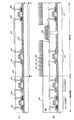
図12に、図11(A)の工程まで終了した時点での、画素の上面図を示す。なお、配線の位置や半導体層の位置を明確にするために、絶縁膜や層間絶縁膜は省略した。図12のA−A’における断面図が、図11(A)のA−A’に示した部分に相当する。
【0113】
図13に、図12のB−B’における断面図を示す。トランジスタTr3は、走査線974の一部であるゲート電極975を有しており、ゲート電極975はトランジスタTr4のゲート電極920とも接続されている。また、トランジスタTr3の半導体層の不純物領域977は、一方は信号線Siとして機能する接続配線942に接続され、もう一方は、接続配線971に接続されている。
【0114】
トランジスタTr1は、容量配線973の一部であるゲート電極976を有しており、ゲート電極976はトランジスタTr2のゲート電極921とも接続されている。また、トランジスタTr1の半導体層の不純物領域978は、一方は接続配線971に接続され、もう一方は、電源線Viとして機能する接続配線943に接続されている。
【0115】
接続配線943は、トランジスタTr2の不純物領域934aにも接続されている。また、970は保持容量であり、半導体層972と、ゲート絶縁膜906と、容量配線973を有している。半導体層972が有する不純物領域979は、接続配線943に接続されている。
【0116】
次に、図11(B)に示すように、画素電極947に対応する位置に開口部を有する第3の層間絶縁膜949を形成する。第3の層間絶縁膜949は絶縁性を有していて、バンクとして機能し、隣接する画素の有機発光層を分離する役割を有している。本実施例ではレジストを用いて第3の層間絶縁膜949を形成する。
【0117】
本実施例では、第3の層間絶縁膜949の厚さを1μm程度とし、開口部は画素電極947に近くなればなるほど広くなる、所謂逆テーパー状になるように形成する。これはレジストを成膜した後、開口部を形成しようとする部分以外をマスクで覆い、UV光を照射して露光し、露光された部分を現像液で除去することによって形成される。
【0118】
本実施例のように、第3の層間絶縁膜949を逆テーパー状にすることで、後の工程において有機発光層を成膜した時に、隣り合う画素同士で有機発光層が分断されるため、有機発光層と、第3の層間絶縁膜949の熱膨張係数が異なっていても、有機発光層がひび割れたり、剥離したりするのを抑えることができる。
【0119】
なお、本実施例においては、第3の層間絶縁膜としてレジストでなる膜を用いているが、場合によっては、ポリイミド、ポリアミド、アクリル、BCB(ベンゾシクロブテン)、酸化珪素膜等を用いることもできる。第3の層間絶縁膜949は絶縁性を有する物質であれば、有機物と無機物のどちらでも良い。
【0120】
次に、有機発光層950を蒸着法により形成し、更に蒸着法により陰極(MgAg電極)951および保護電極952を形成する。このとき有機発光層950及び陰極951を形成するに先立って画素電極947に対して熱処理を施し、水分を完全に除去しておくことが望ましい。なお、本実施例ではOLEDの陰極としてMgAg電極を用いるが、公知の他の材料であっても良い。
【0121】
なお、有機発光層950としては、公知の材料を用いることができる。本実施例では正孔輸送層(Hole transporting layer)及び発光層(Emitting layer)でなる2層構造を有機発光層とするが、正孔注入層、電子注入層若しくは電子輸送層のいずれかを設ける場合もある。このように組み合わせは既に様々な例が報告されており、そのいずれの構成を用いても構わない。
【0122】
本実施例では正孔輸送層としてポリフェニレンビニレンを蒸着法により形成する。また、発光層としては、ポリビニルカルバゾールに1,3,4−オキサジアゾール誘導体のPBDを30〜40%分子分散させたものを蒸着法により形成し、緑色の発光中心としてクマリン6を約1%添加している。
【0123】
また、保護電極952でも有機発光層950を水分や酸素から保護することは可能であるが、さらに好ましくは保護膜953を設けると良い。本実施例では保護膜953として300nm厚の窒化珪素膜を設ける。この保護膜も保護電極952の後に大気解放しないで連続的に形成しても構わない。
【0124】
また、保護電極952は陰極951の劣化を防ぐために設けられ、アルミニウムを主成分とする金属膜が代表的である。勿論、他の材料でも良い。また、有機発光層950、陰極951は非常に水分に弱いので、保護電極952までを大気解放しないで連続的に形成し、外気から有機発光層を保護することが望ましい。
【0125】
なお、有機発光層950の膜厚は10〜400[nm](典型的には60〜150[nm])、陰極951の厚さは80〜200[nm](典型的には100〜150[nm])とすれば良い。
【0126】
こうして図11(B)に示すような構造の発光装置が完成する。なお、画素電極947、有機発光層950、陰極951の重なっている部分954がOLEDに相当する。
【0127】
pチャネル型TFT960及びnチャネル型TFT961は駆動回路が有するTFTであり、CMOSを形成している。トランジスタTr2及びトランジスタTr4は画素部が有するTFTであり、駆動回路のTFTと画素部のTFTとは同一基板上に形成することができる。
【0128】
なお、OLEDを用いた発光装置の場合、駆動回路の電源の電圧が5〜6V程度、最大でも10V程度で十分なので、TFTにおいてホットエレクトロンによる劣化があまり問題にならない。また駆動回路を高速で動作させる必要があるので、TFTのゲート容量は小さいほうが好ましい。よって、本実施例のように、OLEDを用いた発光装置の駆動回路では、TFTの半導体層が有する第2の不純物領域929と、第4の不純物領域933bとが、それぞれゲート電極918、919と重ならない構成にするのが好ましい。
【0129】
本発明の発光装置の作製方法は、本実施例において説明した作製方法に限定されない。本発明の発光装置は公知の方法を用いて作成することが可能である。
【0130】
(実施例2)
本実施例では、実施例1とは異なる発光装置の作製方法について説明する。
【0131】
第2の層間絶縁膜939を形成するまでの工程は、実施例5と同じである。図14(A)に示すように、第2の層間絶縁膜939を形成した後、第2の層間絶縁膜939に接するように、パッシベーション膜981を形成する。
【0132】
パッシベーション膜981は、第2の層間絶縁膜939に含まれる水分が、画素電極947や、第3の層間絶縁膜982を介して、有機発光層950に入るのを防ぐのに効果的である。第2の層間絶縁膜939が有機樹脂材料を有している場合、有機樹脂材料は水分を多く含むため、パッシベーション膜981を設けることは特に有効である。
【0133】
本実施例では、パッシベーション膜981として、窒化珪素膜を用いた。
【0134】
その後、所定のパターンのレジストマスクを形成し、それぞれの半導体層に形成されソース領域またはドレイン領域とする不純物領域に達するコンタクトホールを形成する。コンタクトホールはドライエッチング法で形成する。この場合、まずエッチングガスにCF4、O2の混合ガスを用いてパッシベーション膜981をエッチングし、次にエッチングガスにCF4、O2、Heの混合ガスを用い有機樹脂材料から成る第2の層間絶縁膜939をエッチングし、その後、続いてエッチングガスをCF4、O2として第1の層間絶縁膜937をエッチングする。さらに、半導体層との選択比を高めるために、エッチングガスをCHF3に切り替えて第3の形状のゲート絶縁膜906をエッチングすることによりコンタクトホールを形成することができる。
【0135】
そして、導電性の金属膜をスパッタ法や真空蒸着法で形成し、マスクでパターニングし、その後エッチングすることで、ソース配線940〜943とドレイン配線944〜946を形成する。図示していないが、本実施例ではこの配線を、膜厚50nmのTi膜と、膜厚500nmの合金膜(AlとTiとの合金膜)との積層膜で形成した。
【0136】
次いで、その上に透明導電膜を80〜120nmの厚さで形成し、パターニングすることによって画素電極947を形成する(図14(A))。なお、本実施例では、透明電極として酸化インジウム・スズ(ITO)膜や酸化インジウムに2〜20[%]の酸化亜鉛(ZnO)を混合した透明導電膜を用いる。
【0137】
また、画素電極947は、ドレイン配線946と接して重ねて形成することによってトランジスタTr2のドレイン領域と電気的な接続が形成される。
【0138】
次に、図14(B)に示すように、画素電極947に対応する位置に開口部を有する第3の層間絶縁膜982を形成する。本実施例では、開口部を形成する際、ウエットエッチング法を用いることでテーパー形状の側壁とした。実施例1に示した場合と異なり、第3の層間絶縁膜982上に形成される有機発光層は分断されないため、開口部の側壁が十分になだらかでないと段差に起因する有機発光層の劣化が顕著な問題となってしまうため、注意が必要である。
【0139】
なお、本実施例においては、第3の層間絶縁膜982として酸化珪素でなる膜を用いているが、場合によっては、ポリイミド、ポリアミド、アクリル、BCB(ベンゾシクロブテン)といった有機樹脂膜を用いることもできる。
【0140】
そして、第3の層間絶縁膜982上に有機発光層950を形成する前に、第3の層間絶縁膜982の表面にアルゴンを用いたプラズマ処理を施し、第3の層間絶縁膜982の表面を緻密化しておくのが好ましい。上記構成によって、第3の層間絶縁膜982から有機発光層950に水分が入るのを防ぐことができる。
【0141】
次に、有機発光層950を蒸着法により形成し、更に蒸着法により陰極(MgAg電極)951および保護電極952を形成する。このとき有機発光層950及び陰極951を形成するに先立って画素電極947に対して熱処理を施し、水分を完全に除去しておくことが望ましい。なお、本実施例ではOLEDの陰極としてMgAg電極を用いるが、公知の他の材料であっても良い。
【0142】
なお、有機発光層950としては、公知の材料を用いることができる。本実施例では正孔輸送層(Hole transporting layer)及び発光層(Emitting layer)でなる2層構造を有機発光層とするが、正孔注入層、電子注入層若しくは電子輸送層のいずれかを設ける場合もある。このように組み合わせは既に様々な例が報告されており、そのいずれの構成を用いても構わない。
【0143】
本実施例では正孔輸送層としてポリフェニレンビニレンを蒸着法により形成する。また、発光層としては、ポリビニルカルバゾールに1,3,4−オキサジアゾール誘導体のPBDを30〜40%分子分散させたものを蒸着法により形成し、緑色の発光中心としてクマリン6を約1%添加している。
【0144】
また、保護電極952でも有機発光層950を水分や酸素から保護することは可能であるが、さらに好ましくは保護膜953を設けると良い。本実施例では保護膜953として300nm厚の窒化珪素膜を設ける。この保護膜も保護電極952の後に大気解放しないで連続的に形成しても構わない。
【0145】
また、保護電極952は陰極951の劣化を防ぐために設けられ、アルミニウムを主成分とする金属膜が代表的である。勿論、他の材料でも良い。また、有機発光層950、陰極951は非常に水分に弱いので、保護電極952までを大気解放しないで連続的に形成し、外気から有機発光層を保護することが望ましい。
【0146】
なお、有機発光層950の膜厚は10〜400[nm](典型的には60〜150[nm])、陰極951の厚さは80〜200[nm](典型的には100〜150[nm])とすれば良い。
【0147】
こうして図14(B)に示すような構造の発光装置が完成する。なお、画素電極947、有機発光層950、陰極951の重なっている部分954がOLEDに相当する。
【0148】
pチャネル型TFT960及びnチャネル型TFT961は駆動回路が有するTFTであり、CMOSを形成している。トランジスタTr2及びトランジスタTr4は画素部が有するTFTであり、駆動回路のTFTと画素部のTFTとは同一基板上に形成することができる。
【0149】
本発明の発光装置の作製方法は、本実施例において説明した作製方法に限定されない。本発明の発光装置は公知の方法を用いて作成することが可能である。
【0150】
(実施例3)
本実施例では、図7に示した画素の上面図について説明する。図15に本実施例の画素の上面図を示す。なお、層間絶縁膜やゲート絶縁膜などの各種絶縁膜は、配線や半導体層の位置を明確にするために省略した。また、同じ層に形成される配線は同じハッチで示す。さらに、図15は、画素電極を形成した後で、なおかつ有機発光層を形成する前の画素の上面図に相当する。
【0151】
図15に示す画素は、走査線211と、信号線210と、電源線217を1つづつ有している。そして、走査線211の一部212、213は、それぞれトランジスタTr3と、トランジスタTr4のゲート電極に相当する。
【0152】
トランジスタTr3のソース領域とドレイン領域は、一方は信号線210に接続されており、もう一方は接続配線215を介してトランジスタTr1のドレイン領域に接続されている。また、トランジスタTr4のソース領域とドレイン領域は、一方は接続配線215を介してトランジスタTr1のドレイン領域に接続されており、もう一方は接続配線214を介して容量配線216に接続されている。
【0153】
容量配線216の一部218、220は、トランジスタTr1及びトランジスタTr2のゲート電極に相当する。トランジスタTr1のソース領域は電源線217に接続されている。また、トランジスタTr2のソース領域は電源線217に接続されている。そして、トランジスタTr2のドレイン領域は、接続配線221を介して画素電極222に接続されている。
【0154】
219は保持用量形成用の活性層であり、保持用量形成用の活性層219上には、ゲート絶縁膜(図示せず)を間に挟んで容量配線216が形成されている。この、保持用量形成用の活性層219と、ゲート絶縁膜と、容量配線216が重なっている部分が、保持容量205に相当する。なお、容量配線216上には、間に層間絶縁膜(図示せず)を挟んで、電源線217が形成されている。この容量配線216と、層間絶縁膜と、電源線217が重なる部分に形成される容量を保持容量205として用いても良い。
【0155】
本実施例で示した画素の上面図は、本発明の構成のほんの一例に過ぎず、図7に示した画素の上面図は、本実施例で示した構成に限定されない。なお本実施例は、実施例1または2と自由に組み合わせて実施することが可能である。
【0156】
(実施例4)
本実施例では、図8に示した画素の上面図について説明する。図16に本実施例の画素の上面図を示す。なお、層間絶縁膜やゲート絶縁膜などの各種絶縁膜は、配線や半導体層の位置を明確にするために省略した。また、同じ層に形成される配線は同じハッチで示す。さらに、図16は、画素電極を形成した後で、なおかつ有機発光層を形成する前の画素の上面図に相当する。
【0157】
図16に示す画素は、走査線311と、信号線310と、電源線317を1つづつ有している。そして、走査線311の一部312、313は、それぞれトランジスタTr3と、トランジスタTr4のゲート電極に相当する。
【0158】
トランジスタTr3のソース領域とドレイン領域は、一方は信号線310に接続されており、もう一方は接続配線330を介して容量配線316に接続されている。また、トランジスタTr4のソース領域とドレイン領域は、一方は接続配線330を介して容量配線316に接続されており、もう一方は接続配線315を介してトランジスタTr1のドレイン領域に接続されている。
【0159】
容量配線316の一部318、320は、トランジスタTr1及びトランジスタTr2のゲート電極に相当する。トランジスタTr1のソース領域は電源線317に接続されている。また、トランジスタTr2のソース領域は電源線317に接続されている。そして、トランジスタTr2のドレイン領域は、接続配線321を介して画素電極322に接続されている。
【0160】
319は保持用量形成用の活性層であり、保持用量形成用の活性層319上には、ゲート絶縁膜(図示せず)を間に挟んで容量配線316が形成されている。この、保持用量形成用の活性層319と、ゲート絶縁膜と、容量配線316が重なっている部分が、保持容量305に相当する。なお、容量配線316上には、間に層間絶縁膜(図示せず)を挟んで、電源線317が形成されている。この容量配線316と、層間絶縁膜と、電源線317が重なる部分に形成される容量を保持容量305として用いても良い。
【0161】
本実施例で示した画素の上面図は、本発明の構成のほんの一例に過ぎず、図8に示した画素の上面図は、本実施例で示した構成に限定されない。なお本実施例は、実施例1または2と自由に組み合わせて実施することが可能である。
【0162】
(実施例5)
本実施例では、実施例1とは異なる構成の発光装置について説明する。
【0163】
図27に、本実施例の発光装置の画素部の断面図を示す。図27に示す発光装置は、赤色用の画素(R用画素)800r、緑色用の画素(G用画素)800g、青色用の画素(B用画素)800bを有している。なお、本実施例の構成はカラー表示の発光装置だけではなく、モノクロの画像を表示するための発光装置にも用いることが可能である。
【0164】
各色の画素には、基板830上にトランジスタTr2が形成されている。なお本発明の発光装置では、各画素にトランジスタTr1、Tr2、Tr3、Tr4が形成されているが、図27では特にトランジスタTr2のみ示す。
【0165】
画素電極802r、802g、802b(全てあわせて画素電極802とする)は、ゲート絶縁膜811、第1の層間絶縁膜810、第2の層間絶縁膜807に形成されたコンタクトホールを介して、各トランジスタTr2のドレイン領域809r、809g、809bにそれぞれ接続されている。
【0166】
本実施例において画素電極は陰極であり、光は透過しない。本実施例ではOLEDの陰極としてMgAg電極を用いるが、公知の他の材料であっても良い。
【0167】
そして、画素電極802r、802g、802b及び第2の層間絶縁膜807を覆って、画素電極802r、802g、802bと重なる位置に開口部850を有する第3の層間絶縁膜805が形成される。本実施例においては、第3の層間絶縁膜805として酸化珪素でなる膜を用いているが、場合によっては、ポリイミド、ポリアミド、アクリル、BCB(ベンゾシクロブテン)といった有機樹脂膜を用いることもできる。
【0168】
次に第3層間絶縁膜805の開口部において、画素電極802r、802g、802bと接するように有機発光層803r、803g、803b(全てあわせて有機発光層803とする)を形成する。なおこのとき有機発光層803r、803g、803bはメタルマスクを用いて、色毎に順に蒸着法を用いて形成する。そして各有機発光層803r、803g、803bは、蒸着の際、第3の層間絶縁膜805の開口部以外の部分に多少回り込んで成膜されることも予想されるが、なるべく第3の層間絶縁膜805の開口部においてのみ形成されるようにする。
【0169】
そして次に、蒸着法を用いて、第3の層間絶縁膜805の開口部以外の部分に、金属を有する導電層806を形成する。導電層806の材料としては、低い抵抗の金属であることが望ましい。また、複数の層の導電層を積層して、1つの導電層として用いても良い。本実施例では銅を用いるが、導電層806の材料はこれに限定されず、対向電極よりも抵抗が低い公知の金属材料ならば用いることが可能である。本実施例では、導電層806を形成することで、後に形成される対向電極の抵抗を低くすることができるので、基板の大型化に適しているといえる。
【0170】
次に、有機発光層803r、803g、803b及び導電層806を覆って、透明導電膜からなる対向電極804を形成する。本実施例では、透明導電膜としてITOを用いる。ITOは蒸着法を用いて形成することが可能である。本実施例では特にイオンプレーティング法を用いて形成する場合について説明する。
【0171】
イオンプレーティング法は、蒸着法に分類される気相表面処理技術の1つであり、何らかの方法で蒸発させた蒸着物質を、高周波プラズマあるいは真空放電でイオン化または励起させ、蒸着させる基板に負電位を与えることで該イオンを加速し、基板に付着させる方法である。
【0172】
イオンプレーティング法を用いて対向電極を形成する際の具体的な条件として、0.01〜1Paの不活性ガス雰囲気下において、基板温度を100〜300℃に保って蒸着させることが望ましい。そして70%以上の焼結密度を有する蒸発源としてのITOを用いることが望ましい。なお、イオンプレーティング法を用いる際の最適な条件は、実施者が適宜選択することができる。
【0173】
また高周波プラズマを用いて蒸着物質をイオン化または励起することで、より蒸着物質のイオン化する率または励起する率を高めることができ、なおかつイオン化または励起された蒸着物質が高いエネルギー状態にあるので、速い蒸発速度を有したままで酸素との結合を十分に行うことができる。このため、高速度で良質な膜の形成が可能である。
【0174】
本実施例では上記イオンプレーティング法を用い、透明導電膜からなる対向電極804を80〜120nmの厚さで形成した。本実施例では、透明電極として酸化インジウム・スズ(ITO)膜や酸化インジウムに2〜20[%]の酸化亜鉛(ZnO)を混合した透明導電膜を用いる。
【0175】
なお本実施例の対向電極の形成方法は、上述したイオンプレーティング法に限定されない。ただし、イオンプレーティング法を用いて形成された膜は密着性が高く、また比較的低い温度でも結晶性の高いITO膜を成膜することができるので、ITOの抵抗を低くすることができ、さらに比較的広い面積における均一な成膜が可能であり、基板の大型化に適しているといえる。
【0176】
そして各画素において、R用OLED801r、G用OLED801g、B用OLED801bが完成する。各OLEDは、画素電極802r、802g、802bと、有機発光層803r、803g、803bと、対向電極804とをそれぞれ有している。
【0177】
図28に、本実施例のTFTが形成された基板(素子基板)の上面図を示す。基板830に、画素部831、走査線駆動回路832、信号線駆動回路833、端子834が形成された状態を示している。端子834と各駆動回路、画素部に形成されている電源線及び対向電極は、引き回し配線835で接続されている。
【0178】
また、必要に応じてCPU、メモリーなどを形成したICチップがCOG(Chip on Glass)法などにより素子基板に実装されていても良い。
【0179】
OLEDは導電層806の間に形成され、その構造は図29に示されている。画素電極802は各画素に対応する電極であり、導電層806の間に形成されている。その上層には有機化合物層803が導電層806の間に形成され、複数の画素電極802に渡ってストライプ状に連続的に形成されている。
【0180】
対向電極804は、有機化合物層803及び導電層806の上層に形成され、かつ同様に導電層806と接するように形成されている。
【0181】
引き回し配線835は走査線(図示せず)と同じ層に形成されており、導電層806とは直接接触していない。そして引き回し配線835と対向電極804は重なっている部分においてコンタクトを取っている。
【0182】
本実施例の構成は、実施例3または4と自由に組み合わせて実施することが可能である。
【0183】
(実施例6)
本実施例では、本発明のデジタル駆動法で駆動する発光装置が有する駆動回路(信号線駆動回路及び走査線駆動回路)の構成について説明する。
【0184】
図17に信号線駆動回路601の構成をブロック図で示す。602はシフトレジスタ、603は記憶回路A、604は記憶回路B、605は定電流回路である。
【0185】
シフトレジスタ602にはクロック信号CLKと、スタートパルス信号SPが入力されている。また記憶回路A603にはデジタルビデオ信号(Digital Video Signals)が入力されており、記憶回路B604にはラッチ信号(Latch Signals)が入力されている。定電流回路604から出力される一定の信号電流Icは信号線へ入力される。
【0186】
図18に信号線駆動回路601のより詳しい構成を示す。
【0187】
シフトレジスタ602に所定の配線からクロック信号CLKとスタートパルス信号SPとが入力されることによって、タイミング信号が生成される。タイミング信号は記憶回路A603が有する複数のラッチA(LATA_1〜LATA_x)にそれぞれ入力される。なおこのときシフトレジスタ602において生成されたタイミング信号を、バッファ等で緩衝増幅してから、記憶回路A603が有する複数のラッチA(LATA_1〜LATA_x)にそれぞれ入力するような構成にしても良い。
【0188】
記憶回路A603にタイミング信号が入力されると、該タイミング信号に同期して、ビデオ信号線610に入力される1ビット分のデジタルビデオ信号が、順に複数のラッチA(LATA_1〜LATA_x)のそれぞれに書き込まれ、保持される。
【0189】
なお、本実施例では記憶回路A603にデジタルビデオ信号を取り込む際に、記憶回路A603が有する複数のラッチA(LATA_1〜LATA_x)に、順にデジタルビデオ信号を入力しているが、本発明はこの構成に限定されない。記憶回路A603が有する複数のステージのラッチをいくつかのグループに分け、各グループごとに並行して同時にデジタルビデオ信号を入力する、いわゆる分割駆動を行っても良い。なおこのときのグループの数を分割数と呼ぶ。例えば4つのステージごとにラッチをグループに分けた場合、4分割で分割駆動すると言う。
【0190】
記憶回路A603の全てのステージのラッチへの、デジタルビデオ信号の書き込みが一通り終了するまでの時間を、ライン期間と呼ぶ。実際には、上記ライン期間に水平帰線期間が加えられた期間をライン期間に含むことがある。
【0191】
1ライン期間が終了すると、記憶回路B604が有する複数のラッチB(LATB_1〜LATB_x)に、ラッチ信号線609を介してラッチシグナル(Latch Signal)が供給される。この瞬間、記憶回路A603が有する複数のラッチA(LATA_1〜LATA_x)に保持されているデジタルビデオ信号は、記憶回路B604が有する複数のラッチB(LATB_1〜LATB_x)に一斉に書き込まれ、保持される。
【0192】
デジタルビデオ信号を記憶回路B604に送出し終えた記憶回路A603には、シフトレジスタ602からのタイミング信号に基づき、次の1ビット分のデジタルビデオ信号の書き込みが順次行われる。
【0193】
この2順目の1ライン期間中には、記憶回路B604に書き込まれ、保持されているデジタルビデオ信号が定電流回路605に入力される。
【0194】
定電流回路605は複数の電流設定回路(C1〜Cx)を有している。電流設定回路(C1〜Cx)のそれぞれにデジタルビデオ信号が入力されると、該デジタルビデオ信号が有する1または0の情報によって、信号線に一定の電流Icが流れるか、または信号線に電源線V1〜Vxの電位が与えられるか、いずれか一方が選択される。
【0195】
図19に電流設定回路C1の具体的な構成の一例を示す。なお電流設定回路C2〜Cxも同じ構成を有する。
【0196】
電流設定回路C1は定電流源631と、4つのトランスミッションゲートSW1〜SW4と、2つのインバーターInb1、Inb2とを有している。なお、定電流源631が有するトランジスタ650の極性は、画素が有するトランジスタTr1及びTr2の極性と同じである。
【0197】
記憶回路B604が有するLATB_1から出力されたデジタルビデオ信号によって、SW1〜SW4のスイッチングが制御される。なおSW1及びSW3に入力されるデジタルビデオ信号と、SW2及びSW4に入力されるデジタルビデオ信号は、Inb1、Inb2によって反転している。そのためSW1及びSW3がオンのときはSW2及びSW4はオフ、SW1及びSW3がオフのときはSW2及びSW4はオンとなっている。
【0198】
SW1及びSW3がオンのとき、定電流源631から0ではない所定の値の電流IcがSW1及びSW3を介して信号線S1に入力される。
【0199】
逆にSW2及びSW4がオンのときは、定電流源631からの電流IcはSW2を介してグラウンドに落とされる。またSW4を介して電源線V1〜Vxの電源電位が信号線S1に与えられ、Ic≒0となる。
【0200】
再び図18を参照して、前記の動作が、1ライン期間内に、定電流回路605が有する全ての電流設定回路(C1〜Cx)において同時に行われる。よって、デジタルビデオ信号により、全ての信号線に入力される信号電流Icの値が選択される。
【0201】
次に、走査線駆動回路の構成について説明する。
【0202】
図20は走査線駆動回路641の構成を示すブロック図である。
【0203】
走査線駆動回路641は、それぞれシフトレジスタ642、バッファ643を有している。また場合によってはレベルシフタを有していても良い。
【0204】
走査線駆動回路641において、シフトレジスタ642にクロックCLK及びスタートパルス信号SPが入力されることによって、タイミング信号が生成される。生成されたタイミング信号はバッファ643において緩衝増幅され、対応する走査線に供給される。
【0205】
走査線には、1ライン分の画素の第1スイッチング用TFT及び第2スイッチング用TFTのゲート電極が接続されている。そして、1ライン分の画素の第1スイッチング用TFT及び第2スイッチング用TFTを一斉にONにしなくてはならないので、バッファ643は大きな電流を流すことが可能なものが用いられる。
【0206】
本発明において用いられる駆動回路は、本実施例で示した構成に限定されない。さらに、本実施例で示した定電流回路は、図19に示した構成に限定されない。本発明で用いられる定電流回路は、信号電流Icが取りうる2値のいずれか一方をデジタルビデオ信号によって選択し、選択された値を有する信号電流を信号線に流すことができれば、どのような構成を有していても良い。
【0207】
本実施例の構成は、実施例1〜5と自由に組み合わせて実施することが可能である。
(実施例7)
本実施例では、nビットのデジタルビデオ信号に対応した本発明の発光装置の駆動法において、サブフレーム期間SF1〜SFnの出現する順序について説明する。
【0208】
図21に1フレーム期間において、n個の書き込み期間(Ta1〜Tan)とn個の表示期間(Td1〜Tdn)とが出現するタイミングを示す。横軸は時間を示しており、縦軸は画素が有する走査線の位置を示している。各画素の詳しい動作については実施の形態を参照すれば良いので、ここでは省略する。
【0209】
本実施例の駆動方法では、1フレーム期間中で1番長い表示期間を有するサブフレーム期間(本実施例ではSFn)を、1フレーム期間の最初及び最後に設けない。言い換えると、1フレーム期間中で1番長い表示期間を有するサブフレーム期間の前後に、同じフレーム期間に含まれる他のサブフレーム期間が出現するような構成にしている。
【0210】
上記構成によって、中間階調の表示を行ったときに、隣り合うフレーム期間同士で発光する表示期間が隣接することによって起きていた表示むらを、人間の目に認識されずらくすることができる。
【0211】
なお本実施例の構成はn≧3の場合において有効である。また、本実施例は実施例1〜実施例6と自由に組み合わせて実施することが可能である。
【0212】
(実施例8)
本実施例では、本発明の発光装置を6ビットのデジタルビデオ信号を用いて駆動させる例について説明する。
【0213】
図22に、1フレーム期間において、6個の書き込み期間(Ta1〜Ta6)と6個の表示期間(Td1〜Td6)とが出現するタイミングを示す。横軸は時間を示しており、縦軸は画素が有する走査線の位置を示している。各画素の詳しい動作については実施の形態を参照すれば良いので、ここでは省略する。
【0214】
6ビットのデジタルビデオ信号を用いた駆動する場合、1フレーム期間内に少なくとも6つのサブフレーム期間SF1〜SF6が設けられる。
【0215】
サブフレーム期間SF1〜SF6は、6ビットのデジタル信号の各ビットに対応している。そしてサブフレーム期間SF1〜SF6は、6個の書き込み期間(Ta1〜Ta6)と、6個の表示期間(Td1〜Td6)とを有している。
【0216】
m(mは1〜6の任意の数)ビット目に対応している書き込み期間Tamと表示期間Tdmとを有するサブフレーム期間はSFmとなる。書き込み期間Tamの次には、同じビット数に対応する表示期間、この場合Tdmが出現する。
【0217】
1フレーム期間中に書き込み期間Taと表示期間Tdとが繰り返し出現することで、1つの画像を表示することが可能である。
【0218】
表示期間SF1〜SF6の長さは、SF1:SF2:…:SF6=20:21:…:25を満たす。
【0219】
本発明の駆動方法では、1フレーム期間中における発光する表示期間の長さの和を制御することで、階調を表示する。
【0220】
なお本実施例の構成は、実施例1〜7と自由に組み合わせて実施することが可能である。
【0221】
(実施例9)
本実施例では、nビットのデジタルビデオ信号を用いた、図6、図21とは異なる駆動方法の一例について説明する。
【0222】
図23に、1フレーム期間において、n+1個の書き込み期間(Ta1〜Ta(n+1))とn+1個の表示期間(Td1〜Td(n+1))とが出現するタイミングを示す。横軸は時間を示しており、縦軸は画素が有する走査線の位置を示している。各画素の詳しい動作については実施の形態を参照すれば良いので、ここでは省略する。
【0223】
本実施例ではnビットのデジタルビデオ信号に対応して、1フレーム期間内にn+1のサブフレーム期間SF1〜SFn+1が設けられる。そしてサブフレーム期間SF1〜SFn+1は、n+1個の書き込み期間(Ta1〜Ta(n+1))と、n+1個の表示期間(Td1〜Td(n+1))とを有している。
【0224】
書き込み期間Tam(mは1〜n+1の任意の数)と表示期間Tdmとを有するサブフレーム期間はSFmとなる。書き込み期間Tamの次には、同じビット数に対応する表示期間、この場合Tdmが出現する。
【0225】
サブフレーム期間SF1〜SFn−1は、1〜(n−1)ビットのデジタル信号の各ビットに対応している。サブフレーム期間SFn及びSF(n+1)はnビット目のデジタルビデオ信号に対応している。
【0226】
また本実施例では、同じビットのデジタルビデオ信号に対応するサブフレーム期間SFnとSF(n+1)は連続して出現しない。言い換えると、同じビットのデジタルビデオ信号に対応するサブフレーム期間SFnとSF(n+1)の間に、他のサブフレーム期間が設けられている。
【0227】
1フレーム期間中に書き込み期間Taと表示期間Tdとが繰り返し出現することで、1つの画像を表示することが可能である。
【0228】
表示期間SF1〜SFn+1の長さは、SF1:SF2:…:(SFn+SF(n+1))=20:21:…:2n-1を満たす。
【0229】
本発明の駆動方法では、1フレーム期間中における発光する表示期間の長さの和を制御することで、階調を表示する。
【0230】
本実施例は上記構成によって、中間階調の表示を行ったときに、隣り合うフレーム期間同士で発光する表示期間が隣接することによって起きていた表示むらを、図6及び図21の場合に比べて人間の目に認識されずらくすることができる。
【0231】
なお本実施例では、同じビットに対応するサブフレーム期間が2つある場合について説明したが、本発明はこれに限定されない。1フレーム期間内に同じビットに対応するサブフレーム期間が3つ以上設けられていても良い。
【0232】
また、本実施例では最上位ビットのデジタルビデオ信号に対応するサブフレーム期間を複数設けたが、本発明はこれに限定されない。最上位ビット以外のビットのデジタルビデオ信号に対応するサブフレーム期間を複数設けても良い。また、対応するサブフレーム期間が複数設けられたビットは1つだけに限られず、いくつかのビットのそれぞれに複数のサブフレーム期間が対応するような構成にしても良い。
【0233】
なお本実施例の構成はn≧2の場合において有効である。また、本実施例は実施例1〜8と自由に組み合わせて実施することが可能である。
【0234】
(実施例10)
本実施例では、アナログ駆動法で駆動する本発明の発光装置が有する信号線駆動回路の構成について説明する。なお走査線駆動回路の構成は、実施例6において示した構成を用いることができるので、ここでは説明を省略する。
【0235】
図31(A)に本実施例の信号線駆動回路401のブロック図を示す。402はシフトレジスタ、403はバッファ、404はサンプリング回路、405は電流変換回路を示している。
【0236】
シフトレジスタ402には、クロック信号(CLK)、スタートパルス信号(SP)が入力されている。シフトレジスタ402にクロック信号(CLK)とスタートパルス信号(SP)が入力されると、タイミング信号が生成される。
【0237】
生成されたタイミング信号は、バッファ403において増幅または緩衝増幅されて、サンプリング回路404に入力される。なお、バッファの代わりにレベルシフタを設けて、タイミング信号を増幅しても良い。また、バッファとレベルシフタを両方設けていても良い。
【0238】
図31(B)にサンプリング回路404、電流変換回路405の具体的な構成を示す。なおサンプリング回路404は、端子410においてバッファ403と接続されている。
【0239】
サンプリング回路404には、複数のスイッチ411が設けられている。そしてサンプリング回路404には、ビデオ信号線406からアナログビデオ信号が入力されており、スイッチ411はタイミング信号に同期して、該アナログビデオ信号をサンプリングし、後段の電流変換回路405に入力する。なお図31(B)では、電流変換回路405はサンプリング回路404が有するスイッチ411の1つに接続されている電流変換回路だけを示しているが、各スイッチ411の後段に、図31(B)に示したような電流変換回路405が接続されているものとする。
【0240】
なお本実施例では、スイッチ411にトランジスタを1つだけ用いているが、スイッチ411はタイミング信号に同期してアナログビデオ信号をサンプリングできるスイッチであれば良く、本実施例の構成に限定されない。
【0241】
サンプリングされたアナログビデオ信号は、電流変換回路405が有する電流出力回路412に入力される。電流出力回路412は、入力されたビデオ信号の電圧に見合った値の電流(信号電流)を出力する。なお図31ではアンプ及びTFTを用いて電流出力回路を形成しているが、本発明はこの構成に限定されず、入力された信号の電圧に見合った値の電流を出力することができる回路であれば良い。
【0242】
該信号電流は、同じく電流変換回路405が有するリセット回路417に入力される。リセット回路417は、2つのアナログスイッチ413、414と、インバーター416と、電源415を有している。
【0243】
アナログスイッチ414にはリセット信号(Res)が入力されており、アナログスイッチ413には、インバーター416によって反転されたリセット信号(Res)が入力されている。そしてアナログスイッチ413とアナログスイッチ414は、反転したリセット信号とリセット信号にそれぞれ同期して動作しており、一方がオンのとき片一方がオフになっている。
【0244】
そして、アナログスイッチ413がオンのときに信号電流は対応する信号線に入力される。逆に、アナログスイッチ414がオンのときに電源415の電位が信号線に与えられ、信号線がリセットされる。なお、電源415の電位は、画素に設けられた電源線の電位とほぼ同じ高さであることが望ましく、信号線がリセットされているときに信号線にながれる電流が0に近ければ近いほど良い。
【0245】
なお信号線は、帰線期間中にリセットするのが望ましい。しかし、画像を表示している期間以外であるならば、必要に応じて帰線期間以外の期間にリセットすることも可能である。
【0246】
なお、本発明の発光装置を駆動する信号線駆動回路及び走査線駆動回路は、本実施例で示す構成に限定されない。本実施例の構成は、実施例1〜実施例9に示した構成と自由に組み合わせて実施することが可能である。
【0247】
(実施例11)
本発明において、三重項励起子からの燐光を発光に利用できる有機発光材料を用いることで、外部発光量子効率を飛躍的に向上させることができる。これにより、OLEDの低消費電力化、長寿命化、および軽量化が可能になる。
【0248】
ここで、三重項励起子を利用し、外部発光量子効率を向上させた報告を示す。 (T.Tsutsui, C.Adachi, S.Saito, Photochemical Processes in Organized Molecular Systems, ed.K.Honda, (Elsevier Sci.Pub., Tokyo,1991) p.437.)
【0249】
上記の論文により報告された有機発光材料(クマリン色素)の分子式を以下に示す。
【0250】
【化1】

(M.A.Baldo, D.F.O'Brien, Y.You, A.Shoustikov, S.Sibley, M.E.Thompson, S.R.Forrest, Nature 395 (1998) p.151.)
【0252】
上記の論文により報告された有機発光材料(Pt錯体)の分子式を以下に示す。
【0253】
【化2】
(M.A.Baldo, S.Lamansky, P.E.Burrrows, M.E.Thompson, S.R.Forrest, Appl.Phys.Lett.,75 (1999) p.4.) (T.Tsutsui, M.-J.Yang, M.Yahiro, K.Nakamura, T.Watanabe, T.tsuji, Y.Fukuda, T.Wakimoto, S.Mayaguchi, Jpn.Appl.Phys., 38 (12B) (1999) L1502.)
【0255】
上記の論文により報告された有機発光材料(Ir錯体)の分子式を以下に示す。
【0256】
【化3】
以上のように三重項励起子からの燐光発光を利用できれば原理的には一重項励起子からの蛍光発光を用いる場合より3〜4倍の高い外部発光量子効率の実現が可能となる。
【0258】
なお、本実施例の構成は、実施例1〜実施例10のいずれの構成とも自由に組み合わせて実施することが可能である。
【0259】
(実施例12)
本実施例では、本発明を用いて発光装置を作製した例について、図24を用いて説明する。
【0260】
図24は、TFTが形成された素子基板をシーリング材によって封止することによって形成された発光装置の上面図であり、図24(B)は、図24(A)のA−A’における断面図、図24(C)は図24(A)のB−B’における断面図である。
【0261】
基板4001上に設けられた画素部4002と、信号線駆動回路4003と、第1及び第2の走査線駆動回路4004a、bとを囲むようにして、シール材4009が設けられている。また画素部4002と、信号線駆動回路4003と、第1及び第2の走査線駆動回路4004a、bとの上にシーリング材4008が設けられている。よって画素部4002と、信号線駆動回路4003と、第1及び第2の走査線駆動回路4004a、bとは、基板4001とシール材4009とシーリング材4008とによって、充填材4210で密封されている。
【0262】
また基板4001上に設けられた画素部4002と、信号線駆動回路4003と、第1及び第2の走査線駆動回路4004a、bとは、複数のTFTを有している。図24(B)では代表的に、下地膜4010上に形成された、信号線駆動回路4003に含まれる駆動TFT(但し、ここではnチャネル型TFTとpチャネル型TFTを図示する)4201及び画素部4002に含まれる電流制御用TFT(トランジスタTr2)4202を図示した。
【0263】
本実施例では、駆動TFT4201には公知の方法で作製されたpチャネル型TFTまたはnチャネル型TFTが用いられ、電流制御用TFT4202には公知の方法で作製されたpチャネル型TFTが用いられる。また、画素部4002には電流制御用TFT4202のゲートに接続された保持容量(図示せず)が設けられる。
【0264】
駆動TFT4201及び電流制御用TFT4202上には層間絶縁膜(平坦化膜)4301が形成され、その上に電流制御用TFT4202のドレインと電気的に接続する画素電極(陽極)4203が形成される。画素電極4203としては仕事関数の大きい透明導電膜が用いられる。透明導電膜としては、酸化インジウムと酸化スズとの化合物、酸化インジウムと酸化亜鉛との化合物、酸化亜鉛、酸化スズまたは酸化インジウムを用いることができる。また、前記透明導電膜にガリウムを添加したものを用いても良い。
【0265】
そして、画素電極4203の上には絶縁膜4302が形成され、絶縁膜4302は画素電極4203の上に開口部が形成されている。この開口部において、画素電極4203の上には有機発光層4204が形成される。有機発光層4204は公知の有機発光材料または無機発光材料を用いることができる。また、有機発光材料には低分子系(モノマー系)材料と高分子系(ポリマー系)材料があるがどちらを用いても良い。
【0266】
有機発光層4204の形成方法は公知の蒸着技術もしくは塗布法技術を用いれば良い。また、有機発光層の構造は正孔注入層、正孔輸送層、発光層、電子輸送層または電子注入層を自由に組み合わせて積層構造または単層構造とすれば良い。
【0267】
有機発光層4204の上には遮光性を有する導電膜(代表的にはアルミニウム、銅もしくは銀を主成分とする導電膜またはそれらと他の導電膜との積層膜)からなる陰極4205が形成される。また、陰極4205と有機発光層4204の界面に存在する水分や酸素は極力排除しておくことが望ましい。従って、有機発光層4204を窒素または希ガス雰囲気で形成し、酸素や水分に触れさせないまま陰極4205を形成するといった工夫が必要である。本実施例ではマルチチャンバー方式(クラスターツール方式)の成膜装置を用いることで上述のような成膜を可能とする。そして陰極4205は所定の電圧が与えられている。
【0268】
以上のようにして、画素電極(陽極)4203、有機発光層4204及び陰極4205からなるOLED4303が形成される。そしてOLED4303を覆うように、絶縁膜4302上に保護膜4303が形成されている。保護膜4303は、OLED4303に酸素や水分等が入り込むのを防ぐのに効果的である。
【0269】
4005aは電源供給線に接続された引き回し配線であり、電流制御用TFT4202のソース領域に電気的に接続されている。引き回し配線4005aはシール材4009と基板4001との間を通り、異方導電性フィルム4300を介してFPC4006が有するFPC用配線4301に電気的に接続される。
【0270】
シーリング材4008としては、ガラス材、金属材(代表的にはステンレス材)、セラミックス材、プラスチック材(プラスチックフィルムも含む)を用いることができる。プラスチック材としては、FRP(Fiberglass−Reinforced Plastics)板、PVF(ポリビニルフルオライド)フィルム、マイラーフィルム、ポリエステルフィルムまたはアクリル樹脂フィルムを用いることができる。また、アルミニウムホイルをPVFフィルムやマイラーフィルムで挟んだ構造のシートを用いることもできる。
【0271】
但し、OLEDからの光の放射方向がカバー材側に向かう場合にはカバー材は透明でなければならない。その場合には、ガラス板、プラスチック板、ポリエステルフィルムまたはアクリルフィルムのような透明物質を用いる。
【0272】
また、充填材4210としては窒素やアルゴンなどの不活性な気体の他に、紫外線硬化樹脂または熱硬化樹脂を用いることができ、PVC(ポリビニルクロライド)、アクリル、ポリイミド、エポキシ樹脂、シリコーン樹脂、PVB(ポリビニルブチラル)またはEVA(エチレンビニルアセテート)を用いることができる。本実施例では充填材として窒素を用いた。
【0273】
また充填材4210を吸湿性物質(好ましくは酸化バリウム)もしくは酸素を吸着しうる物質にさらしておくために、シーリング材4008の基板4001側の面に凹部4007を設けて吸湿性物質または酸素を吸着しうる物質4207を配置する。そして、吸湿性物質または酸素を吸着しうる物質4207が飛び散らないように、凹部カバー材4208によって吸湿性物質または酸素を吸着しうる物質4207は凹部4007に保持されている。なお凹部カバー材4208は目の細かいメッシュ状になっており、空気や水分は通し、吸湿性物質または酸素を吸着しうる物質4207は通さない構成になっている。吸湿性物質または酸素を吸着しうる物質4207を設けることで、OLED4303の劣化を抑制できる。
【0274】
図24(C)に示すように、画素電極4203が形成されると同時に、引き回し配線4005a上に接するように導電性膜4203aが形成される。
【0275】
また、異方導電性フィルム4300は導電性フィラー4300aを有している。基板4001とFPC4006とを熱圧着することで、基板4001上の導電性膜4203aとFPC4006上のFPC用配線4301とが、導電性フィラー4300aによって電気的に接続される。
【0276】
本実施例の構成は、実施例1〜実施例11に示した構成と自由に組み合わせて実施することが可能である。
【0277】
(実施例13)
本実施例では、本発明の発光装置の画素の構成の、図2、図7及び図8とは異なる例について説明する。
【0278】
図30(A)に、本実施例の画素の構成を示す。図30(A)に示す画素701は、信号線Si(S1〜Sxのうちの1つ)、第1走査線Gaj(Ga1〜Gayのうちの1つ)、第2走査線Gbj(Gb1〜Gbyのうちの1つ)及び電源線Vi(V1〜Vxのうちの1つ)を有している。なお、画素部に設けられる第1走査線と第2走査線の数は必ずしも同じ数であるとは限らない。
【0279】
また画素701は、トランジスタTr1(第1電流駆動用トランジスタまたは第1のトランジスタ)、トランジスタTr2(第2電流駆動用トランジスタまたは第2のトランジスタ)、トランジスタTr3(第1スイッチング用トランジスタまたは第3のトランジスタ)、トランジスタTr4(第2スイッチング用トランジスタまたは第4のトランジスタ)、トランジスタTr5(消去用トランジスタまたは第5のトランジスタ)、OLED704及び保持容量705を少なくとも有している。
【0280】
トランジスタTr3とトランジスタTr4のゲート電極は、共に第1走査線Gajに接続されている。
【0281】
トランジスタTr3のソース領域とドレイン領域は、一方は信号線Siに、もう一方はトランジスタTr1のドレイン領域に接続されている。またトランジスタTr4のソース領域とドレイン領域は、一方は信号線Siに、もう一方はトランジスタTr1のゲート電極に接続されている。
【0282】
トランジスタTr1とトランジスタTr2のゲート電極は互いに接続されている。また、トランジスタTr1とトランジスタTr2のソース領域は、共に電源線Viに接続されている。
【0283】
トランジスタTr2のドレイン領域は、OLED704が有する画素電極に接続されている。
【0284】
トランジスタTr5のゲート電極は、第2走査線Gbjに接続されている。また、トランジスタTr5のソース領域とドレイン領域は、一方は電源線Viに接続されており、もう一方は、トランジスタTr1及びトランジスタTr2のゲート電極に接続されている。
【0285】
電源線Viの電位(電源電位)は一定の高さに保たれている。また対向電極の電位も、一定の高さに保たれている。
【0286】
なお、トランジスタTr3とトランジスタTr4は、nチャネル型TFTとpチャネル型TFTのどちらでも良い。ただし、トランジスタTr3とトランジスタTr4の極性は同じである。
【0287】
また、トランジスタTr1とトランジスタTr2はnチャネル型TFTとpチャネル型TFTのどちらでも良い。ただし、トランジスタTr1とトランジスタTr2の極性は同じである。そして、陽極を画素電極として用い、陰極を対向電極として用いる場合、トランジスタTr1及びトランジスタTr2をpチャネル型TFTとして用いる。逆に、陽極を対向電極として用い、陰極を画素電極として用いる場合、トランジスタTr1及びトランジスタTr2をnチャネル型TFTとして用いる。
【0288】
また、トランジスタTr5は、nチャネル型TFTとpチャネル型TFTのどちらでも良い。
【0289】
保持容量705はトランジスタTr1及びトランジスタTr2のゲート電極と電源線Viとの間に形成されている。保持容量705はトランジスタTr1及びトランジスタTr2のゲート電極とソース領域の間の電圧(ゲート電圧)をより確実に維持するために設けられているが、必ずしも設ける必要はない。
【0290】
図30(B)に本実施例の画素の別の構成を示す。図30(B)に示す画素711は、信号線Si(S1〜Sxのうちの1つ)、第1走査線Gaj(Ga1〜Gayのうちの1つ)、第2走査線Gbj(Gb1〜Gbyのうちの1つ)及び電源線Vi(V1〜Vxのうちの1つ)を有している。
【0291】
また画素711は、トランジスタTr1(第1電流駆動用トランジスタ)、トランジスタTr2(第2電流駆動用トランジスタ)、トランジスタTr3(第1スイッチング用トランジスタ)、トランジスタTr4(第2スイッチング用トランジスタ)、トランジスタTr5(消去用トランジスタまたは第5のトランジスタ)、OLED714及び保持容量715を少なくとも有している。
【0292】
トランジスタTr3とトランジスタTr4のゲート電極は、共に第1走査線Gajに接続されている。
【0293】
トランジスタTr3のソース領域とドレイン領域は、一方は信号線Siに、もう一方はトランジスタTr1のドレイン領域に接続されている。また、またトランジスタTr4のソース領域とドレイン領域は、一方はトランジスタTr1のドレイン領域に、もう一方はトランジスタTr1のゲート電極に接続されている。
【0294】
トランジスタTr1とトランジスタTr2のゲート電極は互いに接続されている。また、トランジスタTr1とトランジスタTr2のソース領域は、共に電源線Viに接続されている。
【0295】
トランジスタTr2のドレイン領域は、OLED714が有する画素電極に接続されている。電源線Viの電位(電源電位)は一定の高さに保たれている。また対向電極の電位も、一定の高さに保たれている。
【0296】
トランジスタTr5のゲート電極は、第2走査線Gbjに接続されている。また、トランジスタTr5のソース領域とドレイン領域は、一方は電源線Viに接続されており、もう一方は、トランジスタTr1及びトランジスタTr2のゲート電極に接続されている。
【0297】
なお、トランジスタTr3とトランジスタTr4は、nチャネル型TFTとpチャネル型TFTのどちらでも良い。ただし、トランジスタTr3とトランジスタTr4の極性は同じである。
【0298】
また、トランジスタTr1とトランジスタTr2はnチャネル型TFTとpチャネル型TFTのどちらでも良い。ただし、トランジスタTr1とトランジスタTr2の極性は同じである。そして、陽極を画素電極として用い、陰極を対向電極として用いる場合、トランジスタTr1及びトランジスタTr2をpチャネル型TFTとして用いることが好ましい。逆に、陽極を対向電極として用い、陰極を画素電極として用いる場合、トランジスタTr1及びトランジスタTr2をnチャネル型TFTとして用いることが好ましい。
【0299】
また、トランジスタTr5は、nチャネル型TFTとpチャネル型TFTのどちらでも良い。
【0300】
保持容量715はトランジスタTr1及びトランジスタTr2のゲート電極と電源線Viとの間に形成されている。保持容量715はトランジスタTr1及びトランジスタTr2のゲート電極とソース領域の間の電圧(ゲート電圧)をより確実に維持するために設けられているが、必ずしも設ける必要はない。
【0301】
図30(C)に本実施例の画素の別の構成を示す。図30(C)に示す画素721は、信号線Si(S1〜Sxのうちの1つ)、第1走査線Gaj(Ga1〜Gayのうちの1つ)、第2走査線Gbj(Gb1〜Gbyのうちの1つ)及び電源線Vi(V1〜Vxのうちの1つ)を有している。
【0302】
また画素721は、トランジスタTr1(第1電流駆動用トランジスタ)、トランジスタTr2(第2電流駆動用トランジスタ)、トランジスタTr3(第1スイッチング用トランジスタ)、トランジスタTr4(第2スイッチング用トランジスタ)、トランジスタTr5(消去用トランジスタまたは第5のトランジスタ)、OLED724及び保持容量725を少なくとも有している。
【0303】
トランジスタTr3とトランジスタTr4のゲート電極は、共に第1走査線Gajに接続されている。
【0304】
トランジスタTr3のソース領域とドレイン領域は、一方は信号線Siに、もう一方はトランジスタTr1のゲート電極に接続されている。また、またトランジスタTr4のソース領域とドレイン領域は、一方はトランジスタTr1のドレイン領域に、もう一方はトランジスタTr1のゲート電極に接続されている。
【0305】
トランジスタTr1とトランジスタTr2のゲート電極は互いに接続されている。また、トランジスタTr1とトランジスタTr2のソース領域は、共に電源線Viに接続されている。
【0306】
トランジスタTr2のドレイン領域は、OLED724が有する画素電極に接続されている。電源線Viの電位(電源電位)は一定の高さに保たれている。また対向電極の電位も、一定の高さに保たれている。
【0307】
トランジスタTr5のゲート電極は、第2走査線Gbjに接続されている。また、トランジスタTr5のソース領域とドレイン領域は、一方は電源線Viに接続されており、もう一方は、トランジスタTr1及びトランジスタTr2のゲート電極に接続されている。
【0308】
なお、トランジスタTr3とトランジスタTr4は、nチャネル型TFTとpチャネル型TFTのどちらでも良い。ただし、トランジスタTr3とトランジスタTr4の極性は同じである。
【0309】
また、トランジスタTr1とトランジスタTr2はnチャネル型TFTとpチャネル型TFTのどちらでも良い。ただし、トランジスタTr1とトランジスタTr2の極性は同じである。そして、陽極を画素電極として用い、陰極を対向電極として用いる場合、トランジスタTr1及びトランジスタTr2をpチャネル型TFTとして用いることが好ましい。逆に、陽極を対向電極として用い、陰極を画素電極として用いる場合、トランジスタTr1及びトランジスタTr2をnチャネル型TFTとして用いることが好ましい。
【0310】
また、トランジスタTr5は、nチャネル型TFTとpチャネル型TFTのどちらでも良い。
【0311】
保持容量725はトランジスタTr1及びトランジスタTr2のゲート電極と電源線Viとの間に形成されている。保持容量725はトランジスタTr1及びトランジスタTr2のゲート電極とソース領域の間の電圧(ゲート電圧)をより確実に維持するために設けられているが、必ずしも設ける必要はない。
【0312】
なお、図30(A)、(B)、(C)に示した画素を有する発光装置の駆動法は、デジタル駆動法に限られる。そして図30(A)、(B)、(C)に示した画素において、OLED704、714、724が発光しているときに、第2走査線Gbjの電位を制御してトランジスタTr5をオンにすることで、OLED704、714、724を非発光の状態にすることができる。よって、画素へのデジタルビデオ信号の入力と並行して、各画素の表示期間を強制的に終了させることができるので
表示期間を書き込み期間よりも短くすることが可能であり、高いビット数のデジタルビデオ信号を用いて駆動させるのに適している。
【0313】
本実施例の構成は、実施例1、2、5、6、7、8、9、11、12に示した構成と自由に組み合わせて実施することが可能である。
【0314】
(実施例14)
OLEDを用いた発光装置は自発光型であるため、液晶ディスプレイに比べ、明るい場所での視認性に優れ、視野角が広い。従って、様々な電子機器の表示部に用いることができる。
【0315】
本発明の発光装置を用いた電子機器として、ビデオカメラ、デジタルカメラ、ゴーグル型ディスプレイ(ヘッドマウントディスプレイ)、ナビゲーションシステム、音響再生装置(カーオーディオ、オーディオコンポ等)、ノート型パーソナルコンピュータ、ゲーム機器、携帯情報端末(モバイルコンピュータ、携帯電話、携帯型ゲーム機または電子書籍等)、記録媒体を備えた画像再生装置(具体的にはDVD:Digital Versatile Disc等の記録媒体を再生し、その画像を表示しうるディスプレイを備えた装置)などが挙げられる。特に、斜め方向から画面を見る機会が多い携帯情報端末は、視野角の広さが重要視されるため、発光装置を用いることが望ましい。それら電子機器の具体例を図25に示す。
【0316】
図25(A)はOLED表示装置であり、筐体2001、支持台2002、表示部2003、スピーカー部2004、ビデオ入力端子2005等を含む。本発明の発光装置は表示部2003に用いることができる。発光装置は自発光型であるためバックライトが必要なく、液晶ディスプレイよりも薄い表示部とすることができる。なお、OLED表示装置は、パソコン用、TV放送受信用、広告表示用などの全ての情報表示用表示装置が含まれる。
【0317】
図25(B)はデジタルスチルカメラであり、本体2101、表示部2102、受像部2103、操作キー2104、外部接続ポート2105、シャッター2106等を含む。本発明の発光装置は表示部2102に用いることができる。
【0318】
図25(C)はノート型パーソナルコンピュータであり、本体2201、筐体2202、表示部2203、キーボード2204、外部接続ポート2205、ポインティングマウス2206等を含む。本発明の発光装置は表示部2203に用いることができる。
【0319】
図25(D)はモバイルコンピュータであり、本体2301、表示部2302、スイッチ2303、操作キー2304、赤外線ポート2305等を含む。本発明の発光装置は表示部2302に用いることができる。
【0320】
図25(E)は記録媒体を備えた携帯型の画像再生装置(具体的にはDVD再生装置)であり、本体2401、筐体2402、表示部A2403、表示部B2404、記録媒体(DVD等)読み込み部2405、操作キー2406、スピーカー部2407等を含む。表示部A2403は主として画像情報を表示し、表示部B2404は主として文字情報を表示するが、本発明の発光装置はこれら表示部A、B2403、2404に用いることができる。なお、記録媒体を備えた画像再生装置には家庭用ゲーム機器なども含まれる。
【0321】
図25(F)はゴーグル型ディスプレイ(ヘッドマウントディスプレイ)であり、本体2501、表示部2502、アーム部2503を含む。本発明の発光装置は表示部2502に用いることができる。
【0322】
図25(G)はビデオカメラであり、本体2601、表示部2602、筐体2603、外部接続ポート2604、リモコン受信部2605、受像部2606、バッテリー2607、音声入力部2608、操作キー2609等を含む。本発明の発光装置は表示部2602に用いることができる。
【0323】
ここで図25(H)は携帯電話であり、本体2701、筐体2702、表示部2703、音声入力部2704、音声出力部2705、操作キー2706、外部接続ポート2707、アンテナ2708等を含む。本発明の発光装置は表示部2703に用いることができる。なお、表示部2703は黒色の背景に白色の文字を表示することで携帯電話の消費電流を抑えることができる。
【0324】
なお、将来的に有機発光材料の発光輝度が高くなれば、出力した画像情報を含む光をレンズ等で拡大投影してフロント型若しくはリア型のプロジェクターに用いることも可能となる。
【0325】
また、上記電子機器はインターネットやCATV(ケーブルテレビ)などの電子通信回線を通じて配信された情報を表示することが多くなり、特に動画情報を表示する機会が増してきている。有機発光材料の応答速度は非常に高いため、発光装置は動画表示に好ましい。
【0326】
また、発光装置は発光している部分が電力を消費するため、発光部分が極力少なくなるように情報を表示することが望ましい。従って、携帯情報端末、特に携帯電話や音響再生装置のような文字情報を主とする表示部に発光装置を用いる場合には、非発光部分を背景として文字情報を発光部分で形成するように駆動することが望ましい。
【0327】
以上の様に、本発明の適用範囲は極めて広く、あらゆる分野の電子機器に用いることが可能である。また、本実施例の電子機器は実施例1〜13に示したいずれの構成の発光装置を用いても良い。
【0328】
【発明の効果】
【0329】
上述した構成によって、本発明の発光装置は温度変化に左右されずに一定の輝度を得ることができる。また、カラー表示において、各色毎に異なる有機発光材料を有するOLEDを設けた場合でも、温度によって各色のOLEDの輝度がバラバラに変化して所望の色が得られないということを防ぐことができる。
【図面の簡単な説明】
【図1】 本発明の発光装置の上面ブロック図。
【図2】 本発明の発光装置の画素の回路図。
【図3】 走査線に入力される信号のタイミングチャート。
【図4】 駆動における画素の概略図。
【図5】 アナログ駆動法における書き込み期間と表示期間の出現するタイミングを示す図。
【図6】 デジタル駆動法における書き込み期間と表示期間の出現するタイミングを示す図。
【図7】 本発明の発光装置の画素の回路図。
【図8】 本発明の発光装置の画素の回路図。
【図9】 本発明の発光装置の作製方法を示す図。
【図10】 本発明の発光装置の作製方法を示す図。
【図11】 本発明の発光装置の作製方法を示す図。
【図12】 本発明の発光装置の画素の上面図。
【図13】 本発明の発光装置の画素の断面図。
【図14】 本発明の発光装置の作製方法を示す図。
【図15】 本発明の発光装置の画素の上面図。
【図16】 本発明の発光装置の画素の上面図。
【図17】 信号線駆動回路のブロック図。
【図18】 デジタル駆動法における信号線駆動回路の詳細図。
【図19】 デジタル駆動法における電流設定回路の回路図。
【図20】 走査線駆動回路のブロック図。
【図21】 デジタル駆動法における書き込み期間と表示期間の出現するタイミングを示す図。
【図22】 デジタル駆動法における書き込み期間と表示期間の出現するタイミングを示す図。
【図23】 デジタル駆動法における書き込み期間と表示期間の出現するタイミングを示す図。
【図24】 本発明の発光装置の外観図及び断面図。
【図25】 本発明の発光装置を用いた電子機器の図。
【図26】 OLEDの電圧電流特性を示す図。
【図27】 本発明の発光装置の画素の断面図。
【図28】 本発明の発光装置の素子基板の上面図。
【図29】 本発明の発光装置の素子基板の拡大図。
【図30】 本発明の発光装置の画素の回路図。
【図31】 デジタル駆動法における信号線駆動回路の詳細図。[0001]
BACKGROUND OF THE INVENTION
The present invention relates to an OLED panel in which an organic OLED (OLED: Organic Light Emitting Device) formed on a substrate is enclosed between the substrate and a cover material. The present invention also relates to an OLED module in which an IC including a controller is mounted on the OLED panel. In this specification, the OLED panel and the OLED module are collectively referred to as a light emitting device. The present invention further relates to an electronic apparatus using the light emitting device.
[0002]
[Prior art]
The OLED emits light by itself and has high visibility, is not required for a backlight necessary for a liquid crystal display device (LCD), is optimal for thinning, and has no restriction on the viewing angle. Therefore, in recent years, light emitting devices using OLEDs have attracted attention as display devices that replace CRTs and LCDs.
[0003]
The OLED has a layer (hereinafter, referred to as an organic light emitting layer) containing an organic compound (organic light emitting material) capable of obtaining luminescence generated by applying an electric field, an anode layer, and a cathode layer. . Luminescence in organic compounds includes light emission (fluorescence) when returning from the singlet excited state to the ground state and light emission (phosphorescence) when returning from the triplet excited state to the ground state. Any one of the above-described light emission may be used, or both light emission may be used.
[0004]
In this specification, all layers provided between the anode and the cathode of the OLED are defined as organic light emitting layers. Specifically, the organic light emitting layer includes a light emitting layer, a hole injection layer, an electron injection layer, a hole transport layer, an electron transport layer, and the like. Basically, the OLED has a structure in which an anode / light emitting layer / cathode is laminated in this order. In addition to this structure, the anode / hole injection layer / light emitting layer / cathode and the anode / hole injection layer / The light emitting layer / electron transport layer / cathode may be stacked in this order.
[0005]
[Problems to be solved by the invention]
A problem in putting a light-emitting device into practical use has been a decrease in luminance of the OLED due to deterioration of the organic light-emitting material.
[0006]
Organic light-emitting materials are vulnerable to moisture, oxygen, light, and heat, and their deterioration is accelerated by these materials. Specifically, the speed of deterioration depends on the structure of the device that drives the light emitting device, the characteristics of the organic light emitting material, the electrode material, the conditions in the manufacturing process, the driving method of the light emitting device, and the like.
[0007]
Even if the voltage applied to the organic light emitting layer is constant, if the organic light emitting layer is deteriorated, the luminance of the OLED is lowered and the displayed image becomes unclear. In the present specification, a voltage applied to the organic light emitting layer from a pair of electrodes is defined as an OLED drive voltage (Vel).
[0008]
In addition, in the color display method using three types of OLEDs corresponding to R (red), G (green), and B (blue), the organic light emitting material constituting the organic light emitting layer differs depending on the corresponding color of the OLED. . Therefore, the organic light emitting layer of the OLED may deteriorate at a different speed for each corresponding color. In this case, as the time passes, the luminance of the OLED varies from color to color, and an image having a desired color cannot be displayed on the light emitting device.
[0009]
In addition, the temperature of the organic light emitting layer depends on the outside air temperature, the heat generated by the OLED panel itself, etc., but in general, the value of the current flowing through the OLED varies depending on the temperature. FIG. 26 shows changes in the voltage-current characteristics of the OLED when the temperature of the organic light emitting layer is changed. When the voltage is constant, the OLED driving current increases as the temperature of the organic light emitting layer increases. Since the OLED drive current and the luminance of the OLED are in a proportional relationship, the larger the OLED drive current, the higher the luminance of the OLED. Thus, since the luminance of the OLED changes depending on the temperature of the organic light emitting layer, it is difficult to display a desired gradation, and the current consumption of the light emitting device increases as the temperature rises.
[0010]
Furthermore, since the degree of change in the OLED drive current due to temperature changes generally differs depending on the type of organic light-emitting material, the luminance of the OLEDs of each color may vary depending on the temperature in color display. If the luminance balance of each color is lost, a desired color cannot be displayed.
[0011]
In view of the foregoing, it is an object of the present invention to provide a light-emitting device capable of obtaining a certain luminance without being affected by deterioration of the organic light-emitting layer and temperature change, and capable of performing a desired color display. And
[0012]
[Means for Solving the Problems]
The inventor of the present invention pays attention to the fact that the latter causes less decrease in the luminance of the OLED due to deterioration when the OLED drive voltage is kept constant and the light is emitted while the current flowing through the OLED is kept constant. did. In this specification, the current flowing through the OLED is referred to as an OLED drive current (Iel). And it was thought that the change of the brightness | luminance of OLED by deterioration of OLED could be prevented by controlling the brightness | luminance of OLED not by voltage but by electric current.
[0013]
Specifically, in the present invention, a current mirror circuit formed using a transistor is provided for each pixel. Then, the OLED drive current is controlled using the current mirror circuit. The first transistor and the second transistor included in the current mirror circuit are connected so that their drain currents are maintained at substantially the same value regardless of the value of the load resistance.
[0014]
The first transistor has its drain current I 1 Is controlled in the signal line driver circuit. The drain current I of the first transistor 1 Of the drain current I of the second transistor regardless of the value of the load resistance. 2 As a result, the drain current I of the second transistor is consequently reduced. 2 Is controlled in the signal line driver circuit.
[0015]
The second transistor has its drain current I 2 Are connected to flow to the OLED. Therefore, the value of the OLED drive current flowing through the OLED is controlled by the signal line drive circuit regardless of the value of the load resistance. In other words, the OLED drive current can be controlled to a desired value without being affected by differences in transistor characteristics, OLED degradation, or the like.
[0016]
In the present invention, the above configuration can suppress a decrease in luminance of the OLED even when the organic light emitting layer is deteriorated, and as a result, a clear image can be displayed. In addition, in the case of a light emitting device for color display using OLEDs corresponding to each color, even if the organic light emitting layer of the OLED deteriorates at a different speed for each corresponding color, the luminance balance of each color is prevented from being lost. Can display a desired color.
[0017]
Further, the OLED drive current can be controlled to a desired value even if the temperature of the organic light emitting layer depends on the outside air temperature, the heat generated by the OLED panel itself, or the like. Therefore, since the OLED drive current and the luminance of the OLED are proportional, it is possible to suppress the change in the luminance of the OLED, and it is possible to prevent the consumption current from increasing as the temperature rises. Further, in the case of a light emitting device for color display, since it is possible to suppress changes in the brightness of the OLEDs of each color without being influenced by temperature changes, it is possible to prevent the balance of the brightness of each color from being lost and display a desired color. can do.
[0018]
Furthermore, since the degree of change in the OLED drive current due to temperature changes generally differs depending on the type of organic light-emitting material, the luminance of the OLEDs of each color may vary depending on the temperature in color display. However, in the light emitting device of the present invention, a desired luminance can be obtained without being influenced by a temperature change, so that it is possible to prevent the balance of the luminance of each color from being lost and display a desired color.
[0019]
In a general light-emitting device, since the wiring for supplying current to each pixel itself has a resistance, the potential slightly drops depending on the length of the wiring. The drop in potential varies greatly depending on the image to be displayed. In particular, in a plurality of pixels to which current is supplied from the same wiring, when the ratio of pixels having a high number of gradations is increased, the current flowing through the wiring is increased, and a potential drop is noticeable. When the potential drops, the voltage applied to the OLED of each pixel decreases, so the current supplied to each pixel decreases. Therefore, even if an attempt is made to display a certain gradation in a certain pixel, if the number of gradations of other pixels to which current is supplied from the same wiring changes, the current supplied to the certain pixel is accordingly changed. As a result, the number of gradations also changes. However, in the light emitting device of the present invention, the measured value and the reference value can be obtained for each image to be displayed, and the OLED current can be corrected. Therefore, even if the displayed image changes, the desired number of gradations is displayed by the correction. be able to.
[0020]
Note that in the light-emitting device of the present invention, a transistor used for a pixel may be a transistor formed using single crystal silicon, or a thin film transistor using polycrystalline silicon or amorphous silicon.
[0021]
DETAILED DESCRIPTION OF THE INVENTION
(Embodiment 1)
FIG. 1 is a block diagram showing the configuration of the OLED panel of the present invention.
[0022]
In FIG. 1, the signal line driver circuit 102 and the scanning
[0023]
In this specification, the connection means an electrical connection.
[0024]
In FIG. 1, the
[0025]
The power supply lines V1 to Vx are kept at a predetermined potential. Although FIG. 1 shows the configuration of a light emitting device that displays a monochrome image, the present invention may be a light emitting device that displays a color image. In that case, the heights of the potentials of the power supply lines V1 to Vx need not be kept all the same, and may be changed for each corresponding color.
[0026]
FIG. 2 shows a detailed configuration of the
[0027]
The
[0028]
The gate electrodes of the transistors Tr3 and Tr4 are both connected to the scanning line Gj.
[0029]
One of the source region and the drain region of the transistor Tr3 is connected to the signal line Si, and the other is connected to the drain region of the transistor Tr1. One of the source region and the drain region of the transistor Tr4 is connected to the signal line Si, and the other is connected to the gate electrode of the transistor Tr1.
[0030]
The gate electrodes of the transistor Tr1 and the transistor Tr2 are connected to each other. The source regions of the transistors Tr1 and Tr2 are both connected to the power supply line Vi.
[0031]
A drain region of the transistor Tr2 is connected to a pixel electrode included in the
[0032]
The potential of the power supply line Vi (power supply potential) is kept at a constant height. The potential of the counter electrode is also maintained at a constant height.
[0033]
Note that the transistor Tr3 and the transistor Tr4 may be either an n-channel TFT or a p-channel TFT. However, the transistor Tr3 and the transistor Tr4 have the same polarity.
[0034]
The transistors Tr1 and Tr2 may be either n-channel TFTs or p-channel TFTs. However, the transistor Tr1 and the transistor Tr2 have the same polarity. When the anode is used as a pixel electrode and the cathode is used as a counter electrode, the transistor Tr1 and the transistor Tr2 are used as p-channel TFTs. Conversely, when the anode is used as the counter electrode and the cathode is used as the pixel electrode, the transistors Tr1 and Tr2 are used as n-channel TFTs.
[0035]
The
[0036]
Next, driving of the light emitting device of the present invention will be described with reference to FIGS. The driving of the light emitting device of the present invention can be described by being divided into the writing period Ta and the display period Td. FIG. 3 shows a timing chart of each scanning line. The period during which the scanning line is selected, in other words, the period in which all TFTs connected to the scanning line with the gate electrode are on is indicated by ON. Conversely, a period in which no scan line is selected, in other words, a period in which all TFTs connected to the gate electrode of the scan line are in an OFF state is indicated by OFF. 4 shows the transistor Tr in the writing period Ta and the display period Td. 1 And
[0037]
In the writing period Ta, the scanning lines G1 to Gy are sequentially selected as shown in FIG. Based on the potential of the video signal input to the signal line driver circuit 102, a constant current Ic flows between the signal lines S1 to Sx and the power supply lines V1 to Vx. In this specification, the current Ic is referred to as a signal current.
[0038]
FIG. 4A shows a schematic diagram of the
[0039]
[0040]
[Formula 1]
I 1 = ΜC 0 W / L (V GS -V TH ) 2 / 2
[0041]
In
[0042]
The gate electrode of the transistor Tr2 is connected to the gate electrode of the transistor Tr1. The source region of the transistor Tr2 is connected to the source region of the transistor Tr1. Therefore, the gate voltage of the transistor Tr1 becomes the gate voltage of the transistor Tr2 as it is. Therefore, the drain current I of the transistor Tr2 2 Is kept the same as the drain current of the transistor Tr1. That is, I 2 = Ic.
[0043]
The drain current I of the transistor Tr2 2 Flows to the
[0044]
The
[0045]
When the selection of all the scanning lines G1 to Gy is finished and the above operation is performed on the pixels of all the lines, the writing period Ta is finished. When the writing period Ta ends, the display period Td starts.
[0046]
FIG. 3B shows a timing chart of scanning lines in the display period Td. In the display period Td, all the scanning lines G1 to Gy are not selected.
[0047]
FIG. 4B shows a schematic diagram of a pixel in the display period Td.
[0048]
In the display period Td, the drain region of the transistor Tr1 is in a so-called floating state in which no potential is applied from another wiring, a power source, or the like. On the other hand, in the transistor Tr2, V V determined in the writing period Ta GS Is maintained as is. Therefore, the drain current I of the transistor Tr2 2 The value of remains at Ic. Therefore, in the display period Td, the
[0049]
In the case of a driving method using an analog video signal (analog driving method), the magnitude of Ic is determined by the analog video signal, and the
[0050]
FIG. 5 shows an example of a timing chart in the analog driving method. One frame period has y line periods, and each scanning line is selected in each line period. In each line period, a constant current Ic (Ic1 to Icx) flows through each signal line. In FIG. 5, the values of signal currents flowing through the signal lines in the line period Lj (j = 1 to y) are represented as Ic1 [Lj] to Icx [Lj].
[0051]
The start timing of the writing period Ta and the display period Td is shifted for each line, and the timing at which the writing period of each line appears does not overlap. When the display period Td ends for all pixels, one image is displayed.
[0052]
On the other hand, in the case of a time grayscale driving method (digital driving method) using a digital video signal, one image can be displayed by the writing period Ta and the display period Td appearing repeatedly in one frame period. It is. When an image is displayed using an n-bit video signal, at least n writing periods and n display periods are provided in one frame period. The n writing periods (Ta1 to Tan) and the n display periods (Td1 to Tdn) correspond to each bit of the video signal.
[0053]
FIG. 6 shows a timing at which n writing periods (Ta1 to Tan) and n display periods (Td1 to Tdn) appear in one frame period. The horizontal axis indicates time, and the vertical axis indicates the position of the scanning line included in the pixel.
[0054]
Next to the writing period Tam (m is an arbitrary number from 1 to n), a display period corresponding to the same number of bits, in this case Tdm, appears. The writing period Ta and the display period Td are collectively called a subframe period SF. A subframe period having a writing period Tam and a display period Tdm corresponding to the m-th bit is SFm.
[0055]
The lengths of the subframe periods SF1 to SFn are SF1: SF2:...: SFn = 2 0 : 2 1 : ...: 2 n-1 Meet.
[0056]
Note that a subframe period having a long display period may be divided into several parts in order to improve image quality on display. A specific method of division is disclosed in Japanese Patent Application No. 2000-267164, and may be referred to.
[0057]
In the driving method shown in FIG. 6, gradation is displayed by controlling the sum of the lengths of the display periods during which light is emitted in one frame period.
[0058]
In the present invention, the above configuration can suppress a decrease in luminance of the OLED even when the organic light emitting layer is deteriorated, and as a result, a clear image can be displayed. In addition, in the case of a light emitting device for color display using OLEDs corresponding to each color, even if the organic light emitting layer of the OLED deteriorates at a different speed for each corresponding color, the luminance balance of each color is prevented from being lost. Can display a desired color.
[0059]
Further, the OLED drive current can be controlled to a desired value even if the temperature of the organic light emitting layer depends on the outside air temperature, the heat generated by the OLED panel itself, or the like. Therefore, since the OLED drive current and the luminance of the OLED are proportional, it is possible to suppress the change in the luminance of the OLED, and it is possible to prevent the consumption current from increasing as the temperature rises. Further, in the case of a light emitting device for color display, since it is possible to suppress changes in the brightness of the OLEDs of each color without being influenced by temperature changes, it is possible to prevent the balance of the brightness of each color from being lost and display a desired color. can do.
[0060]
Furthermore, since the degree of change in the OLED drive current due to temperature changes generally differs depending on the type of organic light-emitting material, the luminance of the OLEDs of each color may vary depending on the temperature in color display. However, in the light emitting device of the present invention, a desired luminance can be obtained without being influenced by a temperature change, so that it is possible to prevent the balance of the luminance of each color from being lost and display a desired color.
[0061]
In a general light-emitting device, since the wiring for supplying current to each pixel itself has a resistance, the potential slightly drops depending on the length of the wiring. The drop in potential varies greatly depending on the image to be displayed. In particular, in a plurality of pixels to which current is supplied from the same wiring, when the ratio of pixels having a high number of gradations is increased, the current flowing through the wiring is increased, and a potential drop is noticeable. When the potential drops, the voltage applied to the OLED of each pixel decreases, so the current supplied to each pixel decreases. Therefore, even if an attempt is made to display a certain gradation in a certain pixel, if the number of gradations of other pixels to which current is supplied from the same wiring changes, the current supplied to the certain pixel is accordingly changed. As a result, the number of gradations also changes. However, in the light emitting device of the present invention, the measured value and the reference value can be obtained for each image to be displayed, and the OLED current can be corrected. Therefore, even if the displayed image changes, the desired number of gradations is displayed by the correction. be able to.
[0062]
(Embodiment 2)
In this embodiment, a structure different from that in FIG. 2 of the
[0063]
FIG. 7 shows a configuration of a pixel of this embodiment mode. The
[0064]
The
[0065]
The gate electrodes of the transistors Tr3 and Tr4 are both connected to the scanning line Gj.
[0066]
One of the source region and the drain region of the transistor Tr3 is connected to the signal line Si, and the other is connected to the drain region of the transistor Tr1. One of the source region and the drain region of the transistor Tr4 is connected to the drain region of the transistor Tr1, and the other is connected to the gate electrode of the transistor Tr1.
[0067]
The gate electrodes of the transistor Tr1 and the transistor Tr2 are connected to each other. The source regions of the transistors Tr1 and Tr2 are both connected to the power supply line Vi.
[0068]
A drain region of the transistor Tr2 is connected to a pixel electrode included in the
[0069]
Note that the transistor Tr3 and the transistor Tr4 may be either an n-channel TFT or a p-channel TFT. However, the transistor Tr3 and the transistor Tr4 have the same polarity.
[0070]
The transistors Tr1 and Tr2 may be either n-channel TFTs or p-channel TFTs. However, the transistor Tr1 and the transistor Tr2 have the same polarity. When the anode is used as a pixel electrode and the cathode is used as a counter electrode, it is preferable to use the transistor Tr1 and the transistor Tr2 as p-channel TFTs. Conversely, when the anode is used as the counter electrode and the cathode is used as the pixel electrode, it is preferable to use the transistors Tr1 and Tr2 as n-channel TFTs.
[0071]
The
[0072]
The operation of the light-emitting device including the pixel illustrated in FIG. 7 can be described by being divided into the writing period Ta and the display period Td as in the case of the pixel illustrated in FIG. The operation of the pixel in the writing period Ta and the display period Td is the same as that of the pixel shown in FIG. 2, and the description in FIGS. 3 and 4 of
[0073]
(Embodiment 3)
In this embodiment, a structure of the
[0074]
FIG. 8 shows a configuration of a pixel of this embodiment mode. The
[0075]
The
[0076]
The gate electrodes of the transistors Tr3 and Tr4 are both connected to the scanning line Gj.
[0077]
One of the source region and the drain region of the transistor Tr3 is connected to the signal line Si, and the other is connected to the gate electrode of the transistor Tr1. Also The One of the source region and the drain region of the transistor Tr4 is connected to the drain region of the transistor Tr1, and the other is connected to the gate electrode of the transistor Tr1.
[0078]
The gate electrodes of the transistor Tr1 and the transistor Tr2 are connected to each other. The source regions of the transistors Tr1 and Tr2 are both connected to the power supply line Vi.
[0079]
A drain region of the transistor Tr2 is connected to a pixel electrode included in the
[0080]
Note that the transistor Tr3 and the transistor Tr4 may be either an n-channel TFT or a p-channel TFT. However, the transistor Tr3 and the transistor Tr4 have the same polarity.
[0081]
The transistors Tr1 and Tr2 may be either n-channel TFTs or p-channel TFTs. However, the transistor Tr1 and the transistor Tr2 have the same polarity. When the anode is used as a pixel electrode and the cathode is used as a counter electrode, it is preferable to use the transistor Tr1 and the transistor Tr2 as p-channel TFTs. Conversely, when the anode is used as the counter electrode and the cathode is used as the pixel electrode, it is preferable to use the transistors Tr1 and Tr2 as n-channel TFTs.
[0082]
The
[0083]
The operation of the light-emitting device having the pixel shown in FIG. 8 can be described by being divided into the writing period Ta and the display period Td, as in the case of the pixel shown in FIG. The operation of the pixel in the writing period Ta and the display period Td is the same as that of the pixel shown in FIG. 2, and the description in FIGS. 3 and 4 of
[0084]
【Example】
Examples of the present invention will be described below.
[0085]
Example 1
An example of a method for manufacturing a light-emitting device of the present invention will be described with reference to FIGS. Here, as a typical example, a method for simultaneously manufacturing the transistor Tr2 and the transistor Tr4 of the pixel shown in FIG. 2 and the TFT of the driving portion provided in the periphery of the pixel portion will be described in detail according to the process. Note that the transistor Tr1 and the transistor Tr3 can also be manufactured according to the manufacturing method of the transistor Tr2 and the transistor Tr4. In addition, the pixels illustrated in FIGS. 7, 8, and 30 can be manufactured using the manufacturing process described in this embodiment.
[0086]
First, in this embodiment, a
[0087]
Next, as illustrated in FIG. 9A, a base film 901 formed of an insulating film such as a silicon oxide film, a silicon nitride film, or a silicon oxynitride film is formed over a
[0088]
Next, semiconductor layers 902 to 905 are formed over the base film 901. The semiconductor layers 902 to 905 are formed by forming a semiconductor film having an amorphous structure by a known means (sputtering method, LPCVD method, plasma CVD method, or the like), and then known crystallization treatment (laser crystallization method, heat A crystalline semiconductor film obtained by performing a crystallization method or a thermal crystallization method using a catalyst such as nickel) is formed by patterning into a desired shape. The semiconductor layers 902 to 905 are formed with a thickness of 25 to 80 nm (preferably 30 to 60 nm). The material of the crystalline semiconductor film is not limited, but is preferably silicon (silicon) or silicon germanium (Si X Ge 1-X (X = 0.0001 to 0.02)) It may be formed of an alloy or the like. In this example, a 55 nm amorphous silicon film was formed by plasma CVD, and then a solution containing nickel was held on the amorphous silicon film. This amorphous silicon film is dehydrogenated (500 ° C., 1 hour), then thermally crystallized (550 ° C., 4 hours), and further laser annealed to improve crystallization. Thus, a crystalline silicon film was formed. Then, semiconductor layers 902 to 905 were formed by patterning the crystalline silicon film using a photolithography method.
[0089]
Further, after the semiconductor layers 902 to 905 are formed, the semiconductor layers 902 to 905 may be doped with a small amount of impurity elements (boron or phosphorus) in order to control the threshold value of the TFT.
[0090]
When a crystalline semiconductor film is formed by laser crystallization, a pulse oscillation type or continuous emission type excimer laser, YAG laser, YVO Four A laser can be used. When these lasers are used, it is preferable to use a method in which laser light emitted from a laser oscillator is linearly collected by an optical system and irradiated onto a semiconductor film. Crystallization conditions are appropriately selected by the practitioner, but when an excimer laser is used, the pulse oscillation frequency is 300 Hz and the laser energy density is 100 to 400 mJ / cm. 2 (Typically 200-300mJ / cm 2 ). When a YAG laser is used, the second harmonic is used and the pulse oscillation frequency is set to 30 to 300 kHz, and the laser energy density is set to 300 to 600 mJ / cm. 2 (Typically 350-500mJ / cm 2 ) Then, when the laser beam condensed linearly with a width of 100 to 1000 μm, for example 400 μm, is irradiated over the entire surface of the substrate, the superposition ratio (overlap ratio) of the linear laser light at this time is 50 to 90%. Good.
[0091]
Next, a
[0092]
When a silicon oxide film is used, TEOS (Tetraethyl Orthosilicate) and O 2 The reaction pressure is 40 Pa, the substrate temperature is 300 to 400 ° C., and the high frequency (13.56 MHz) power density is 0.5 to 0.8 W / cm. 2 And can be formed by discharging. The silicon oxide film thus manufactured can obtain good characteristics as a gate insulating film by thermal annealing at 400 to 500 ° C. thereafter.
[0093]
Then, a heat-resistant
[0094]
On the other hand, when a Ta film is used for the heat-resistant
[0095]
Next, a resist
[0096]
[0097]
Then, a first doping process is performed to add an impurity element of one conductivity type to the semiconductor layer. Here, a step of adding an impurity element imparting n-type is performed. The
[0098]
In this step, depending on doping conditions, impurities may flow under the first shape
[0099]
Next, a second etching process is performed as shown in FIG. Similarly, the etching process is performed by an ICP etching apparatus, and CF is used as an etching gas. Four And Cl 2 RF power of 3.2 W / cm 2 (13.56 MHz), bias power 45 mW / cm 2 Etching is performed at 13.56 MHz and a pressure of 1.0 Pa.
[0100]
Then, an impurity element imparting n-type conductivity is doped under a condition of a high acceleration voltage with a dose amount lower than that in the first doping treatment. For example, the acceleration voltage is 70 to 120 keV and 1 × 10 13 / Cm 2
[0101]
As shown in FIG. 10B, impurity regions 933 (933a, 933b) and 934 (934a, 934a, 934a, 934a, 934a, 933a, 933b, 934a, 934a, 933a, 933b, and 934a) 934b). Also in this case, an impurity element imparting p-type is added using the second shape
[0102]
However, the impurity regions 933 and 934 can be divided into two regions containing an impurity element imparting n-type in detail. The
[0103]
After that, as illustrated in FIG. 10C, a first
[0104]
Then, a step of activating the impurity element imparting n-type or p-type added at each concentration is performed. This step is performed by a thermal annealing method using a furnace annealing furnace. In addition, a laser annealing method or a rapid thermal annealing method (RTA method) can be applied. In the thermal annealing method, the oxygen concentration is 1 ppm or less, preferably 0.1 ppm or less in a nitrogen atmosphere at 400 to 700 ° C., typically 500 to 600 ° C. In this example, the temperature is 550 ° C. for 4 hours. Heat treatment was performed. In addition, when a plastic substrate having a low heat resistant temperature is used for the
[0105]
Subsequent to the activation step, the step of hydrogenating the semiconductor layer is performed by changing the atmosphere gas and performing heat treatment at 300 to 450 ° C. for 1 to 12 hours in an atmosphere containing 3 to 100% hydrogen. This step is performed in the semiconductor layer by thermally excited hydrogen. 16 -10 18 /cm Three This is a step of terminating the dangling bond. As another means of hydrogenation, plasma hydrogenation (using hydrogen excited by plasma) may be performed. In any case, the defect density in the semiconductor layers 902 to 905 is 10 16 /cm Three It is desirable to set it as follows, and for that purpose, hydrogen may be added at about 0.01 to 0.1 atomic%.
[0106]
Then, a second
[0107]
Thus, the surface can be satisfactorily planarized by forming the second
[0108]
Thereafter, a resist mask having a predetermined pattern is formed, and contact holes are formed in the respective semiconductor layers to reach impurity regions serving as source regions or drain regions. The contact hole is formed by a dry etching method. In this case, CF Four , O 2 , The second
[0109]
Then, a conductive metal film is formed by a sputtering method or a vacuum deposition method, patterned with a mask, and then etched to form source wirings 940 to 943 and
[0110]
Next, a transparent conductive film is formed thereon with a thickness of 80 to 120 nm and patterned to form a pixel electrode 947 (FIG. 11A). In this embodiment, an indium tin oxide (ITO) film or a transparent conductive film in which 2 to 20% zinc oxide (ZnO) is mixed with indium oxide is used as the transparent electrode.
[0111]
Further, the
[0112]
FIG. 12 is a top view of a pixel at the time when the process up to FIG. 11A is completed. Note that the insulating film and the interlayer insulating film are omitted in order to clarify the position of the wiring and the position of the semiconductor layer. A cross-sectional view taken along the line AA ′ in FIG. 12 corresponds to the portion indicated by AA ′ in FIG.
[0113]
FIG. 13 is a cross-sectional view taken along the line BB ′ of FIG. The transistor Tr3 includes a
[0114]
The transistor Tr1 includes a
[0115]
The
[0116]
Next, as illustrated in FIG. 11B, a third
[0117]
In this embodiment, the thickness of the third
[0118]
As in this example, by forming the third
[0119]
In this embodiment, a film made of a resist is used as the third interlayer insulating film. However, in some cases, a polyimide, polyamide, acrylic, BCB (benzocyclobutene), silicon oxide film, or the like may be used. it can. The third
[0120]
Next, the organic
[0121]
Note that a known material can be used for the organic
[0122]
In this embodiment, polyphenylene vinylene is formed by a vapor deposition method as a hole transport layer. The light-emitting layer is formed by vapor deposition of 30-40% PBD of 1,3,4-oxadiazole derivative in polyvinyl carbazole, and about 1% of coumarin 6 is used as a green emission center. It is added.
[0123]
In addition, the
[0124]
The
[0125]
The thickness of the organic
[0126]
Thus, a light emitting device having a structure as shown in FIG. 11B is completed. Note that a
[0127]
A p-channel TFT 960 and an n-channel TFT 961 are TFTs included in the driver circuit and form a CMOS. The transistor Tr2 and the transistor Tr4 are TFTs included in the pixel portion, and the TFT of the driver circuit and the TFT of the pixel portion can be formed over the same substrate.
[0128]
Note that in the case of a light emitting device using OLED, the power supply voltage of the driving circuit is about 5 to 6 V, and about 10 V at the maximum is sufficient, so that deterioration due to hot electrons in the TFT is not a problem. Further, since it is necessary to operate the driving circuit at high speed, it is preferable that the gate capacitance of the TFT is small. Therefore, as in this embodiment, in the driving circuit of the light emitting device using the OLED, the
[0129]
The manufacturing method of the light-emitting device of the present invention is not limited to the manufacturing method described in this embodiment. The light emitting device of the present invention can be manufactured using a known method.
[0130]
(Example 2)
In this embodiment, a method for manufacturing a light-emitting device, which is different from that in
[0131]
The steps until the second
[0132]
The
[0133]
In this embodiment, a silicon nitride film is used as the
[0134]
Thereafter, a resist mask having a predetermined pattern is formed, and contact holes are formed in the respective semiconductor layers to reach impurity regions serving as source regions or drain regions. The contact hole is formed by a dry etching method. In this case, CF Four , O 2 The
[0135]
Then, a conductive metal film is formed by a sputtering method or a vacuum deposition method, patterned with a mask, and then etched to form source wirings 940 to 943 and
[0136]
Next, a transparent conductive film is formed thereon with a thickness of 80 to 120 nm and patterned to form a pixel electrode 947 (FIG. 14A). In this embodiment, an indium tin oxide (ITO) film or a transparent conductive film in which 2 to 20% zinc oxide (ZnO) is mixed with indium oxide is used as the transparent electrode.
[0137]
Further, the
[0138]
Next, as shown in FIG. 14B, a third
[0139]
In this embodiment, a film made of silicon oxide is used as the third
[0140]
Then, before forming the organic
[0141]
Next, the organic
[0142]
Note that a known material can be used for the organic
[0143]
In this embodiment, polyphenylene vinylene is formed by a vapor deposition method as a hole transport layer. The light-emitting layer is formed by vapor deposition of 30-40% PBD of 1,3,4-oxadiazole derivative in polyvinyl carbazole, and about 1% of coumarin 6 is used as a green emission center. It is added.
[0144]
In addition, the
[0145]
The
[0146]
The thickness of the organic
[0147]
Thus, a light emitting device having a structure as shown in FIG. 14B is completed. Note that a
[0148]
A p-channel TFT 960 and an n-channel TFT 961 are TFTs included in the driver circuit and form a CMOS. The transistor Tr2 and the transistor Tr4 are TFTs included in the pixel portion, and the TFT of the driver circuit and the TFT of the pixel portion can be formed over the same substrate.
[0149]
The manufacturing method of the light-emitting device of the present invention is not limited to the manufacturing method described in this embodiment. The light emitting device of the present invention can be manufactured using a known method.
[0150]
(Example 3)
In this embodiment, a top view of the pixel shown in FIG. 7 will be described. FIG. 15 shows a top view of the pixel of this embodiment. Note that various insulating films such as an interlayer insulating film and a gate insulating film were omitted in order to clarify the positions of wirings and semiconductor layers. Further, wirings formed in the same layer are indicated by the same hatch. Further, FIG. 15 corresponds to a top view of the pixel after the pixel electrode is formed and before the organic light emitting layer is formed.
[0151]
The pixel shown in FIG. 15 has one
[0152]
One of the source region and the drain region of the transistor Tr3 is connected to the
[0153]
[0154]
[0155]
The top view of the pixel shown in this embodiment is merely an example of the structure of the present invention, and the top view of the pixel shown in FIG. 7 is not limited to the structure shown in this embodiment. Note that this embodiment can be implemented by being freely combined with
[0156]
(Example 4)
In this embodiment, a top view of the pixel shown in FIG. 8 will be described. FIG. 16 shows a top view of the pixel of this embodiment. Note that various insulating films such as an interlayer insulating film and a gate insulating film were omitted in order to clarify the positions of wirings and semiconductor layers. Further, wirings formed in the same layer are indicated by the same hatch. Further, FIG. 16 corresponds to a top view of the pixel after the pixel electrode is formed and before the organic light emitting layer is formed.
[0157]
The pixel shown in FIG. 16 has one
[0158]
One of a source region and a drain region of the transistor Tr3 is connected to the
[0159]
[0160]
[0161]
The top view of the pixel shown in this embodiment is only an example of the structure of the present invention, and the top view of the pixel shown in FIG. 8 is not limited to the structure shown in this embodiment. Note that this embodiment can be implemented by being freely combined with
[0162]
(Example 5)
In this example, a light-emitting device having a configuration different from that of Example 1 will be described.
[0163]
FIG. 27 shows a cross-sectional view of the pixel portion of the light emitting device of this embodiment. The light-emitting device shown in FIG. 27 includes a red pixel (R pixel) 800r, a green pixel (G pixel) 800g, and a blue pixel (B pixel) 800b. Note that the structure of this embodiment can be used not only for a color display light-emitting device but also for a light-emitting device for displaying a monochrome image.
[0164]
A transistor Tr2 is formed on the
[0165]
The pixel electrodes 802r, 802g, and 802b (all together referred to as a pixel electrode 802) are connected to each other through contact holes formed in the gate insulating film 811, the first interlayer insulating film 810, and the second interlayer insulating film 807. The transistors Tr2 are connected to the drain regions 809r, 809g, and 809b, respectively.
[0166]
In this embodiment, the pixel electrode is a cathode and does not transmit light. In this embodiment, an MgAg electrode is used as the cathode of the OLED, but other known materials may be used.
[0167]
Then, a third interlayer insulating film 805 having an opening 850 at a position overlapping the pixel electrodes 802r, 802g, and 802b is formed so as to cover the pixel electrodes 802r, 802g, and 802b and the second interlayer insulating film 807. In this embodiment, a film made of silicon oxide is used as the third interlayer insulating film 805. However, an organic resin film such as polyimide, polyamide, acrylic, or BCB (benzocyclobutene) can be used depending on circumstances. .
[0168]
Next, organic light emitting layers 803r, 803g, and 803b (all together referred to as an organic light emitting layer 803) are formed so as to be in contact with the pixel electrodes 802r, 802g, and 802b in the opening of the third interlayer insulating film 805. At this time, the organic light emitting layers 803r, 803g, and 803b are formed by using a metal mask and sequentially using a vapor deposition method for each color. Each of the organic light emitting layers 803r, 803g, and 803b is expected to be formed slightly around the portion other than the opening portion of the third interlayer insulating film 805 at the time of vapor deposition. It is formed only at the opening of the insulating film 805.
[0169]
Next, a
[0170]
Next, a
[0171]
The ion plating method is one of vapor phase surface treatment techniques classified as a vapor deposition method. A vapor deposition material evaporated by some method is ionized or excited by high-frequency plasma or vacuum discharge, and a negative potential is applied to a substrate to be vapor deposited. Is applied to accelerate the ions to adhere to the substrate.
[0172]
As specific conditions for forming the counter electrode by using the ion plating method, it is desirable to perform deposition while maintaining the substrate temperature at 100 to 300 ° C. in an inert gas atmosphere of 0.01 to 1 Pa. It is desirable to use ITO as an evaporation source having a sintered density of 70% or more. Note that the practitioner can appropriately select the optimum conditions for using the ion plating method.
[0173]
In addition, ionization or excitation of the deposition material using high-frequency plasma can increase the rate of ionization or excitation of the deposition material, and the ionized or excited deposition material is in a high energy state, so that it is fast. Bonding with oxygen can be sufficiently performed while maintaining the evaporation rate. For this reason, it is possible to form a high-quality film at a high speed.
[0174]
In this example, the above-described ion plating method was used to form a
[0175]
In addition, the formation method of the counter electrode of a present Example is not limited to the ion plating method mentioned above. However, the film formed using the ion plating method has high adhesion, and an ITO film having high crystallinity can be formed even at a relatively low temperature, so that the resistance of ITO can be lowered. Furthermore, uniform film formation over a relatively large area is possible, which can be said to be suitable for increasing the size of the substrate.
[0176]
In each pixel, the R OLED 801r, the G OLED 801g, and the B OLED 801b are completed. Each OLED has pixel electrodes 802r, 802g, and 802b, organic light emitting layers 803r, 803g, and 803b, and a
[0177]
FIG. 28 shows a top view of a substrate (element substrate) on which the TFT of this example is formed. A state where a
[0178]
Further, an IC chip on which a CPU, a memory, and the like are formed may be mounted on the element substrate by a COG (Chip on Glass) method or the like as necessary.
[0179]
The OLED is formed between the
[0180]
The
[0181]
The
[0182]
The configuration of the present embodiment can be implemented by freely combining with the third or fourth embodiment.
[0183]
(Example 6)
In this embodiment, a structure of a driver circuit (a signal line driver circuit and a scan line driver circuit) included in a light-emitting device driven by the digital driving method of the present invention will be described.
[0184]
FIG. 17 is a block diagram illustrating the configuration of the signal line driver circuit 601. Reference numeral 602 denotes a shift register,
[0185]
A clock signal CLK and a start pulse signal SP are input to the shift register 602. A digital video signal (Digital Video Signals) is input to the
[0186]
FIG. 18 shows a more detailed configuration of the signal line driver circuit 601.
[0187]
When the clock signal CLK and the start pulse signal SP are input to the shift register 602 from a predetermined wiring, a timing signal is generated. The timing signal is input to each of the plurality of latches A (LATA_1 to LATA_x) included in the memory circuit A603. Note that at this time, the timing signal generated in the shift register 602 may be buffered and amplified by a buffer or the like and then input to the plurality of latches A (LATA_1 to LATA_x) included in the memory circuit A603.
[0188]
When a timing signal is input to the
[0189]
In this embodiment, when a digital video signal is taken into the memory circuit A603, the digital video signal is sequentially input to the plurality of latches A (LATA_1 to LATA_x) included in the memory circuit A603. It is not limited to. A plurality of stages of latches included in the
[0190]
The time until the digital video signal is completely written to the latches of all the stages of the
[0191]
When one line period ends, a latch signal (Latch Signal) is supplied to the plurality of latches B (LATB_1 to LATB_x) included in the memory circuit B604 through the
[0192]
After the digital video signal has been sent to the
[0193]
During the second line period, the digital video signal written and held in the
[0194]
The constant
[0195]
FIG. 19 shows an example of a specific configuration of the current setting circuit C1. The current setting circuits C2 to Cx have the same configuration.
[0196]
The current setting circuit C1 includes a constant
[0197]
Switching of SW1 to SW4 is controlled by a digital video signal output from LATB_1 included in the memory circuit B604. The digital video signal input to SW1 and SW3 and the digital video signal input to SW2 and SW4 are inverted by Inb1 and Inb2. Therefore, when SW1 and SW3 are on, SW2 and SW4 are off, and when SW1 and SW3 are off, SW2 and SW4 are on.
[0198]
When SW1 and SW3 are on, a current Ic having a predetermined value other than 0 is input from the constant
[0199]
Conversely, when SW2 and SW4 are on, the current Ic from the constant
[0200]
Referring to FIG. 18 again, the above operation is simultaneously performed in all the current setting circuits (C1 to Cx) included in constant
[0201]
Next, the configuration of the scanning line driving circuit will be described.
[0202]
FIG. 20 is a block diagram illustrating a configuration of the scanning line driving circuit 641.
[0203]
The scanning line driver circuit 641 includes a shift register 642 and a buffer 643, respectively. In some cases, a level shifter may be provided.
[0204]
In the scan line driver circuit 641, when the clock CLK and the start pulse signal SP are input to the shift register 642, a timing signal is generated. The generated timing signal is buffered and amplified in the buffer 643 and supplied to the corresponding scanning line.
[0205]
A gate electrode of the first switching TFT and the second switching TFT of a pixel for one line is connected to the scanning line. Since the first switching TFT and the second switching TFT of the pixels for one line must be turned on all at once, a buffer 643 that can flow a large current is used.
[0206]
The drive circuit used in the present invention is not limited to the configuration shown in this embodiment. Furthermore, the constant current circuit shown in this embodiment is not limited to the configuration shown in FIG. The constant current circuit used in the present invention can select any one of the binary values that can be taken by the signal current Ic by a digital video signal, and can cause any signal current having the selected value to flow through the signal line. You may have a structure.
[0207]
The structure of a present Example can be implemented combining freely with Examples 1-5.
(Example 7)
In this embodiment, the order in which the subframe periods SF1 to SFn appear in the driving method of the light emitting device of the present invention corresponding to the n-bit digital video signal will be described.
[0208]
FIG. 21 shows a timing at which n writing periods (Ta1 to Tan) and n display periods (Td1 to Tdn) appear in one frame period. The horizontal axis indicates time, and the vertical axis indicates the position of the scanning line included in the pixel. The detailed operation of each pixel may be referred to the embodiment, and is omitted here.
[0209]
In the driving method of this embodiment, the subframe period (SFn in this embodiment) having the longest display period in one frame period is not provided at the beginning and end of one frame period. In other words, another subframe period included in the same frame period appears before and after the subframe period having the longest display period in one frame period.
[0210]
With the above-described configuration, it is possible to make it difficult for human eyes to recognize display unevenness that occurs due to adjacent display periods that emit light between adjacent frame periods when intermediate grayscale display is performed.
[0211]
The configuration of this embodiment is effective when n ≧ 3. In addition, this embodiment can be implemented by freely combining with
[0212]
(Example 8)
In this embodiment, an example in which the light-emitting device of the present invention is driven using a 6-bit digital video signal will be described.
[0213]
FIG. 22 shows the timing at which six writing periods (Ta1 to Ta6) and six display periods (Td1 to Td6) appear in one frame period. The horizontal axis indicates time, and the vertical axis indicates the position of the scanning line included in the pixel. The detailed operation of each pixel may be referred to the embodiment, and is omitted here.
[0214]
When driving using a 6-bit digital video signal, at least six subframe periods SF1 to SF6 are provided in one frame period.
[0215]
The subframe periods SF1 to SF6 correspond to each bit of the 6-bit digital signal. The subframe periods SF1 to SF6 have six writing periods (Ta1 to Ta6) and six display periods (Td1 to Td6).
[0216]
The sub-frame period having the writing period Tam and the display period Tdm corresponding to the m (m is an arbitrary number from 1 to 6) bit is SFm. Next to the writing period Tam, a display period corresponding to the same number of bits, in this case Tdm, appears.
[0217]
By repeatedly appearing the writing period Ta and the display period Td in one frame period, one image can be displayed.
[0218]
The lengths of the display periods SF1 to SF6 are SF1: SF2:...: SF6 = 2. 0 : 2 1 : ...: 2 Five Meet.
[0219]
In the driving method of the present invention, gradation is displayed by controlling the sum of the lengths of the display periods during which light is emitted in one frame period.
[0220]
In addition, the structure of a present Example can be implemented combining freely with Examples 1-7.
[0221]
Example 9
In this embodiment, an example of a driving method using an n-bit digital video signal different from those in FIGS. 6 and 21 will be described.
[0222]
FIG. 23 shows the timing at which n + 1 writing periods (Ta1 to Ta (n + 1)) and n + 1 display periods (Td1 to Td (n + 1)) appear in one frame period. The horizontal axis indicates time, and the vertical axis indicates the position of the scanning line included in the pixel. The detailed operation of each pixel may be referred to the embodiment, and is omitted here.
[0223]
In this embodiment, n + 1 subframe periods SF1 to SFn + 1 are provided in one frame period corresponding to an n-bit digital video signal. The subframe periods SF1 to SFn + 1 have n + 1 writing periods (Ta1 to Ta (n + 1)) and n + 1 display periods (Td1 to Td (n + 1)).
[0224]
A subframe period having a writing period Tam (m is an arbitrary number from 1 to n + 1) and a display period Tdm is SFm. Next to the writing period Tam, a display period corresponding to the same number of bits, in this case Tdm, appears.
[0225]
The subframe periods SF1 to SFn-1 correspond to each bit of the digital signal of 1 to (n-1) bits. The subframe periods SFn and SF (n + 1) correspond to the nth bit digital video signal.
[0226]
In this embodiment, the subframe periods SFn and SF (n + 1) corresponding to the same bit digital video signal do not appear continuously. In other words, another subframe period is provided between subframe periods SFn and SF (n + 1) corresponding to digital video signals of the same bit.
[0227]
By repeatedly appearing the writing period Ta and the display period Td in one frame period, one image can be displayed.
[0228]
The length of the display periods SF1 to SFn + 1 is SF1: SF2:...: (SFn + SF (n + 1)) = 2 0 : 2 1 : ...: 2 n-1 Meet.
[0229]
In the driving method of the present invention, gradation is displayed by controlling the sum of the lengths of the display periods during which light is emitted in one frame period.
[0230]
In the present embodiment, the display unevenness caused by the adjacent display periods emitting light in the adjacent frame periods when the intermediate gradation display is performed is compared with the case of FIGS. It can be difficult to be recognized by human eyes.
[0231]
In this embodiment, the case where there are two subframe periods corresponding to the same bit has been described, but the present invention is not limited to this. Three or more subframe periods corresponding to the same bit may be provided in one frame period.
[0232]
In this embodiment, a plurality of subframe periods corresponding to the most significant bit digital video signal are provided. However, the present invention is not limited to this. A plurality of subframe periods corresponding to digital video signals of bits other than the most significant bit may be provided. Further, the number of bits provided with a plurality of corresponding subframe periods is not limited to one, and a configuration in which a plurality of subframe periods correspond to each of some bits may be employed.
[0233]
The configuration of this embodiment is effective when n ≧ 2. In addition, this embodiment can be implemented by freely combining with Embodiments 1-8.
[0234]
(Example 10)
In this embodiment, a structure of a signal line driver circuit included in the light-emitting device of the present invention driven by an analog driving method will be described. Note that the structure shown in Embodiment 6 can be used as the structure of the scanning line driver circuit, and thus the description thereof is omitted here.
[0235]
FIG. 31A is a block diagram of the signal line driver circuit 401 of this embodiment. Reference numeral 402 denotes a shift register, 403 denotes a buffer, 404 denotes a sampling circuit, and 405 denotes a current conversion circuit.
[0236]
A clock signal (CLK) and a start pulse signal (SP) are input to the shift register 402. When a clock signal (CLK) and a start pulse signal (SP) are input to the shift register 402, a timing signal is generated.
[0237]
The generated timing signal is amplified or buffer amplified in the buffer 403 and input to the
[0238]
FIG. 31B illustrates specific structures of the
[0239]
The
[0240]
In this embodiment, only one transistor is used for the
[0241]
The sampled analog video signal is input to a
[0242]
The signal current is input to a
[0243]
A reset signal (Res) is input to the
[0244]
When the
[0245]
Note that the signal line is desirably reset during the return period. However, if it is outside the period during which the image is displayed, it can be reset to a period other than the blanking period as necessary.
[0246]
Note that the signal line driver circuit and the scan line driver circuit for driving the light-emitting device of the present invention are not limited to the structures shown in this embodiment. The configuration of the present embodiment can be implemented by freely combining with the configurations shown in the first to ninth embodiments.
[0247]
(Example 11)
In the present invention, by using an organic light emitting material that can use phosphorescence from triplet excitons for light emission, the external light emission quantum efficiency can be dramatically improved. Thereby, low power consumption, long life, and light weight of the OLED can be achieved.
[0248]
Here, a report of using triplet excitons to improve the external emission quantum efficiency is shown. (T. Tsutsui, C. Adachi, S. Saito, Photochemical Processes in Organized Molecular Systems, ed. K. Honda, (Elsevier Sci. Pub., Tokyo, 1991) p.437.)
[0249]
The molecular formula of the organic light-emitting material (coumarin dye) reported by the above paper is shown below.
[0250]
[Chemical 1]
(MABaldo, DFO'Brien, Y.You, A.Shoustikov, S.Sibley, METhompson, SRForrest, Nature 395 (1998) p.151.)
[0252]
The molecular formula of the organic light-emitting material (Pt complex) reported by the above paper is shown below.
[0253]
[Chemical formula 2]
(MABaldo, S. Lamansky, PEBurrrows, METhompson, SRForrest, Appl.Phys.Lett., 75 (1999) p.4.) (T.Tsutsui, M.-J.Yang, M.Yahiro, K.Nakamura, T Watanabe, T.tsuji, Y.Fukuda, T.Wakimoto, S.Mayaguchi, Jpn.Appl.Phys., 38 (12B) (1999) L1502.)
[0255]
The molecular formula of the organic light-emitting material (Ir complex) reported by the above paper is shown below.
[0256]
[Chemical 3]
As described above, if phosphorescence emission from triplet excitons can be used, in principle, it is possible to realize an external emission quantum efficiency that is 3 to 4 times higher than that in the case of using fluorescence emission from singlet excitons.
[0258]
In addition, the structure of a present Example can be implemented in combination with any structure of Example 1- Example 10 freely.
[0259]
Example 12
In this example, an example in which a light-emitting device is manufactured using the present invention will be described with reference to FIGS.
[0260]
FIG. 24 is a top view of a light emitting device formed by sealing an element substrate on which a TFT is formed with a sealing material, and FIG. 24B is a cross-sectional view taken along line AA ′ in FIG. FIG. 24C is a cross-sectional view taken along the line BB ′ of FIG.
[0261]
A
[0262]
The
[0263]
In this embodiment, a p-channel TFT or an n-channel TFT manufactured by a known method is used for the driving
[0264]
An interlayer insulating film (planarization film) 4301 is formed on the driving
[0265]
An insulating
[0266]
As a method for forming the organic light emitting layer 4204, a known vapor deposition technique or coating technique may be used. The structure of the organic light emitting layer may be a laminated structure or a single layer structure by freely combining a hole injection layer, a hole transport layer, a light emitting layer, an electron transport layer, or an electron injection layer.
[0267]
On the organic light emitting layer 4204, a
[0268]
As described above, the
[0269]
Reference numeral 4005 a denotes a lead wiring connected to the power supply line, and is electrically connected to the source region of the
[0270]
As the sealing
[0271]
However, when the emission direction of light from the OLED is directed toward the cover material, the cover material must be transparent. In that case, a transparent material such as a glass plate, a plastic plate, a polyester film or an acrylic film is used.
[0272]
As the
[0273]
In order to expose the
[0274]
As shown in FIG. 24C, the
[0275]
The anisotropic
[0276]
The configuration of the present embodiment can be implemented by freely combining the configurations shown in
[0277]
(Example 13)
In this embodiment, an example of the pixel structure of the light-emitting device of the present invention, which is different from those in FIGS. 2, 7, and 8, will be described.
[0278]
FIG. 30A shows the structure of the pixel of this example. A pixel 701 illustrated in FIG. 30A includes a signal line Si (one of S1 to Sx), a first scanning line Gaj (one of Ga1 to Gay), and a second scanning line Gbj (Gb1 to Gby). And a power supply line Vi (one of V1 to Vx). Note that the number of first scanning lines and second scanning lines provided in the pixel portion is not necessarily the same.
[0279]
The pixel 701 includes a transistor Tr1 (first current driving transistor or first transistor), a transistor Tr2 (second current driving transistor or second transistor), and a transistor Tr3 (first switching transistor or third transistor). ), A transistor Tr4 (second switching transistor or fourth transistor), a transistor Tr5 (erasing transistor or fifth transistor), an
[0280]
The gate electrodes of the transistors Tr3 and Tr4 are both connected to the first scanning line Gaj.
[0281]
One of the source region and the drain region of the transistor Tr3 is connected to the signal line Si, and the other is connected to the drain region of the transistor Tr1. One of the source region and the drain region of the transistor Tr4 is connected to the signal line Si, and the other is connected to the gate electrode of the transistor Tr1.
[0282]
The gate electrodes of the transistor Tr1 and the transistor Tr2 are connected to each other. The source regions of the transistors Tr1 and Tr2 are both connected to the power supply line Vi.
[0283]
A drain region of the transistor Tr2 is connected to a pixel electrode included in the
[0284]
The gate electrode of the transistor Tr5 is connected to the second scanning line Gbj. One of the source region and the drain region of the transistor Tr5 is connected to the power supply line Vi, and the other is connected to the gate electrodes of the transistors Tr1 and Tr2.
[0285]
The potential of the power supply line Vi (power supply potential) is kept at a constant height. The potential of the counter electrode is also maintained at a constant height.
[0286]
Note that the transistor Tr3 and the transistor Tr4 may be either an n-channel TFT or a p-channel TFT. However, the transistor Tr3 and the transistor Tr4 have the same polarity.
[0287]
The transistors Tr1 and Tr2 may be either n-channel TFTs or p-channel TFTs. However, the transistor Tr1 and the transistor Tr2 have the same polarity. When the anode is used as a pixel electrode and the cathode is used as a counter electrode, the transistor Tr1 and the transistor Tr2 are used as p-channel TFTs. Conversely, when the anode is used as the counter electrode and the cathode is used as the pixel electrode, the transistors Tr1 and Tr2 are used as n-channel TFTs.
[0288]
The transistor Tr5 may be either an n-channel TFT or a p-channel TFT.
[0289]
The
[0290]
FIG. 30B illustrates another structure of the pixel of this example. A pixel 711 shown in FIG. 30B includes a signal line Si (one of S1 to Sx), a first scanning line Gaj (one of Ga1 to Gay), and a second scanning line Gbj (Gb1 to Gby). And a power supply line Vi (one of V1 to Vx).
[0291]
The pixel 711 includes a transistor Tr1 (first current driving transistor), a transistor Tr2 (second current driving transistor), a transistor Tr3 (first switching transistor), a transistor Tr4 (second switching transistor), and a transistor Tr5 ( An erasing transistor or a fifth transistor), an
[0292]
The gate electrodes of the transistors Tr3 and Tr4 are both connected to the first scanning line Gaj.
[0293]
One of the source region and the drain region of the transistor Tr3 is connected to the signal line Si, and the other is connected to the drain region of the transistor Tr1. One of the source region and the drain region of the transistor Tr4 is connected to the drain region of the transistor Tr1, and the other is connected to the gate electrode of the transistor Tr1.
[0294]
The gate electrodes of the transistor Tr1 and the transistor Tr2 are connected to each other. The source regions of the transistors Tr1 and Tr2 are both connected to the power supply line Vi.
[0295]
A drain region of the transistor Tr2 is connected to a pixel electrode included in the
[0296]
The gate electrode of the transistor Tr5 is connected to the second scanning line Gbj. One of the source region and the drain region of the transistor Tr5 is connected to the power supply line Vi, and the other is connected to the gate electrodes of the transistors Tr1 and Tr2.
[0297]
Note that the transistor Tr3 and the transistor Tr4 may be either an n-channel TFT or a p-channel TFT. However, the transistor Tr3 and the transistor Tr4 have the same polarity.
[0298]
The transistors Tr1 and Tr2 may be either n-channel TFTs or p-channel TFTs. However, the transistor Tr1 and the transistor Tr2 have the same polarity. When the anode is used as a pixel electrode and the cathode is used as a counter electrode, it is preferable to use the transistor Tr1 and the transistor Tr2 as p-channel TFTs. Conversely, when the anode is used as the counter electrode and the cathode is used as the pixel electrode, it is preferable to use the transistors Tr1 and Tr2 as n-channel TFTs.
[0299]
The transistor Tr5 may be either an n-channel TFT or a p-channel TFT.
[0300]
The
[0301]
FIG. 30C illustrates another structure of the pixel of this example. A pixel 721 illustrated in FIG. 30C includes a signal line Si (one of S1 to Sx), a first scanning line Gaj (one of Ga1 to Gay), and a second scanning line Gbj (Gb1 to Gby). And a power supply line Vi (one of V1 to Vx).
[0302]
The pixel 721 includes a transistor Tr1 (first current driving transistor), a transistor Tr2 (second current driving transistor), a transistor Tr3 (first switching transistor), a transistor Tr4 (second switching transistor), and a transistor Tr5 ( An erasing transistor or a fifth transistor), an
[0303]
The gate electrodes of the transistors Tr3 and Tr4 are both connected to the first scanning line Gaj.
[0304]
One of the source region and the drain region of the transistor Tr3 is connected to the signal line Si, and the other is connected to the gate electrode of the transistor Tr1. One of the source region and the drain region of the transistor Tr4 is connected to the drain region of the transistor Tr1, and the other is connected to the gate electrode of the transistor Tr1.
[0305]
The gate electrodes of the transistor Tr1 and the transistor Tr2 are connected to each other. The source regions of the transistors Tr1 and Tr2 are both connected to the power supply line Vi.
[0306]
A drain region of the transistor Tr2 is connected to a pixel electrode included in the
[0307]
The gate electrode of the transistor Tr5 is connected to the second scanning line Gbj. One of the source region and the drain region of the transistor Tr5 is connected to the power supply line Vi, and the other is connected to the gate electrodes of the transistors Tr1 and Tr2.
[0308]
Note that the transistor Tr3 and the transistor Tr4 may be either an n-channel TFT or a p-channel TFT. However, the transistor Tr3 and the transistor Tr4 have the same polarity.
[0309]
The transistors Tr1 and Tr2 may be either n-channel TFTs or p-channel TFTs. However, the transistor Tr1 and the transistor Tr2 have the same polarity. When the anode is used as a pixel electrode and the cathode is used as a counter electrode, it is preferable to use the transistor Tr1 and the transistor Tr2 as p-channel TFTs. Conversely, when the anode is used as the counter electrode and the cathode is used as the pixel electrode, it is preferable to use the transistors Tr1 and Tr2 as n-channel TFTs.
[0310]
The transistor Tr5 may be either an n-channel TFT or a p-channel TFT.
[0311]
The
[0312]
Note that the driving method of the light-emitting device having the pixels shown in FIGS. 30A, 30B, and 30C is limited to the digital driving method. Then, in the pixels shown in FIGS. 30A, 30B, and 30C, when the
The display period can be shorter than the writing period, which is suitable for driving using a digital video signal having a high bit number.
[0313]
The configuration of this embodiment can be implemented by freely combining the configurations shown in
[0314]
(Example 14)
Since a light emitting device using an OLED is a self-luminous type, it is superior in visibility in a bright place and has a wide viewing angle as compared with a liquid crystal display. Therefore, it can be used for display portions of various electronic devices.
[0315]
As an electronic device using the light emitting device of the present invention, a video camera, a digital camera, a goggle type display (head mounted display), a navigation system, a sound reproduction device (car audio, audio component, etc.), a notebook type personal computer, a game device, A portable information terminal (mobile computer, cellular phone, portable game machine, electronic book, etc.), an image playback device equipped with a recording medium (specifically, a DVD: Digital Versatile Disc or other recording medium is played back, and the image is displayed. And a device equipped with a display that can be used. In particular, it is desirable to use a light-emitting device for a portable information terminal that often has an opportunity to see a screen from an oblique direction because the wide viewing angle is important. Specific examples of these electronic devices are shown in FIGS.
[0316]
FIG. 25A illustrates an OLED display device which includes a
[0317]
FIG. 25B illustrates a digital still camera, which includes a
[0318]
FIG. 25C shows a laptop personal computer, which includes a
[0319]
FIG. 25D illustrates a mobile computer, which includes a
[0320]
FIG. 25E shows a portable image reproducing device (specifically, a DVD reproducing device) provided with a recording medium, which includes a
[0321]
FIG. 25F illustrates a goggle type display (head mounted display), which includes a
[0322]
FIG. 25G illustrates a video camera, which includes a main body 2601, a
[0323]
FIG. 25H shows a mobile phone, which includes a
[0324]
If the light emission luminance of the organic light emitting material is increased in the future, the light including the output image information can be enlarged and projected by a lens or the like and used in a front type or rear type projector.
[0325]
In addition, the electronic devices often display information distributed through electronic communication lines such as the Internet and CATV (cable television), and in particular, opportunities to display moving image information are increasing. Since the organic light emitting material has a very high response speed, the light emitting device is preferable for displaying moving images.
[0326]
In addition, since the light emitting device consumes power in the light emitting portion, it is desirable to display information so that the light emitting portion is minimized. Therefore, when a light emitting device is used for a display unit mainly including character information, such as a portable information terminal, particularly a mobile phone or a sound reproduction device, it is driven so that character information is formed by the light emitting part with the non-light emitting part as the background. It is desirable to do.
[0327]
As described above, the applicable range of the present invention is so wide that it can be used for electronic devices in various fields. In addition, the electronic device of this embodiment may use the light emitting device having any structure shown in
[0328]
【The invention's effect】
[0329]
With the above-described structure, the light-emitting device of the present invention can obtain a certain luminance without being influenced by a temperature change. Further, in color display, even when an OLED having a different organic light emitting material for each color is provided, it is possible to prevent a desired color from being obtained because the luminance of the OLED of each color varies with temperature.
[Brief description of the drawings]
FIG. 1 is a top block diagram of a light-emitting device of the present invention.
FIG. 2 is a circuit diagram of a pixel of a light emitting device of the present invention.
FIG. 3 is a timing chart of signals input to scanning lines.
FIG. 4 is a schematic diagram of a pixel in driving.
FIG. 5 is a diagram showing timings at which a writing period and a display period appear in an analog driving method.
FIG. 6 is a diagram showing timings at which a writing period and a display period appear in the digital driving method.
FIG. 7 is a circuit diagram of a pixel of a light emitting device of the present invention.
FIG. 8 is a circuit diagram of a pixel of the light emitting device of the present invention.
9A and 9B illustrate a method for manufacturing a light-emitting device of the present invention.
10A and 10B illustrate a method for manufacturing a light-emitting device of the present invention.
11A to 11C illustrate a method for manufacturing a light-emitting device of the present invention.
FIG. 12 is a top view of a pixel of a light-emitting device of the present invention.
13 is a cross-sectional view of a pixel of a light-emitting device of the present invention.
14A to 14C illustrate a method for manufacturing a light-emitting device of the present invention.
FIG. 15 is a top view of a pixel of a light-emitting device of the present invention.
FIG. 16 is a top view of a pixel of a light-emitting device of the present invention.
FIG. 17 is a block diagram of a signal line driver circuit.
FIG. 18 is a detailed diagram of a signal line driver circuit in a digital driving method.
FIG. 19 is a circuit diagram of a current setting circuit in the digital driving method.
FIG. 20 is a block diagram of a scan line driver circuit.
FIG. 21 is a diagram showing timings at which a writing period and a display period appear in the digital driving method.
FIG. 22 is a diagram showing timings at which a writing period and a display period appear in the digital driving method.
FIG. 23 is a diagram showing timings at which a writing period and a display period appear in the digital driving method.
24A and 24B are an external view and a cross-sectional view of a light-emitting device of the present invention.
FIG. 25 is a diagram of an electronic device using the light-emitting device of the present invention.
FIG. 26 is a diagram showing voltage-current characteristics of an OLED.
FIG. 27 is a cross-sectional view of a pixel of a light-emitting device of the present invention.
FIG. 28 is a top view of an element substrate of a light-emitting device of the present invention.
FIG. 29 is an enlarged view of an element substrate of the light-emitting device of the present invention.
FIG. 30 is a circuit diagram of a pixel of a light-emitting device of the present invention.
FIG. 31 is a detailed diagram of a signal line driver circuit in a digital driving method.
Claims (6)
前記第1のトランジスタのゲートは、前記第2のトランジスタのゲートと電気的に接続され、
前記第1のトランジスタのソース又はドレインの一方は、第1の配線と電気的に接続され、
前記第2のトランジスタのソース又はドレインの一方は、前記第1の配線と電気的に接続され、
前記第2のトランジスタのソース又はドレインの他方は、前記発光素子の画素電極と電気的に接続され、
前記第3のトランジスタのゲートは、第2の配線と電気的に接続され、
前記第3のトランジスタのソース又はドレインの一方は、第3の配線と電気的に接続され、
前記第3のトランジスタのソース又はドレインの他方は、前記容量素子の一方の電極と直接接続され、
前記第4のトランジスタのゲートは、前記第2の配線と電気的に接続され、
前記第4のトランジスタのソース又はドレインの一方は、前記第1のトランジスタのゲートと電気的に接続され、
前記第4のトランジスタのソース又はドレインの他方は、前記第1のトランジスタのソース又はドレインの他方と電気的に接続され、
前記容量素子の一方の電極は、前記第4のトランジスタのソース又はドレインの一方と直接接続され、
前記容量素子の他方の電極は、前記第1の配線と電気的に接続されていることを特徴とする発光装置。A first transistor, a second transistor, a third transistor, a fourth transistor, a capacitor, and a light-emitting element;
A gate of the first transistor is electrically connected to a gate of the second transistor;
One of a source and a drain of the first transistor is electrically connected to the first wiring;
One of a source and a drain of the second transistor is electrically connected to the first wiring;
The other of the source and the drain of the second transistor is electrically connected to the pixel electrode of the light emitting element,
A gate of the third transistor is electrically connected to the second wiring;
One of a source and a drain of the third transistor is electrically connected to a third wiring;
The other of the source and the drain of the third transistor is directly connected to one electrode of the capacitor,
A gate of the fourth transistor is electrically connected to the second wiring;
One of a source and a drain of the fourth transistor is electrically connected to a gate of the first transistor;
The other of the source and the drain of the fourth transistor is electrically connected to the other of the source and the drain of the first transistor;
One electrode of the capacitor is directly connected to one of a source or a drain of the fourth transistor,
The other electrode of the capacitor element is electrically connected to the first wiring.
第5のトランジスタをさらに有し、
前記第5のトランジスタのゲートは、第4の配線と電気的に接続され、
前記第5のトランジスタのソース又はドレインの一方は、前記第1の配線と電気的に接続され、
前記第5のトランジスタのソース又はドレインの他方は、前記第1のトランジスタのゲートと電気的に接続されていることを特徴とする発光装置。In claim 1 ,
A fifth transistor;
A gate of the fifth transistor is electrically connected to a fourth wiring;
One of a source and a drain of the fifth transistor is electrically connected to the first wiring;
The other of the source and the drain of the fifth transistor is electrically connected to the gate of the first transistor.
前記第1及び第2のトランジスタは飽和領域で動作していることを特徴とする発光装置。In claim 1 or claim 2 ,
The light-emitting device, wherein the first and second transistors operate in a saturation region.
前記第3のトランジスタの極性と前記第4のトランジスタの極性とが同じであることを特徴とする発光装置。In any one of Claim 1 thru | or 3 ,
A light-emitting device, wherein the polarity of the third transistor and the polarity of the fourth transistor are the same.
前記第1のトランジスタの極性と前記第2のトランジスタの極性とが同じであることを特徴とする発光装置。In any one of Claims 1 thru | or 4 ,
The light emitting device, wherein the polarity of the first transistor and the polarity of the second transistor are the same.
前記第3の配線と電気的に接続された回路を有し、
前記回路は、前記回路に入力されるデジタルビデオ信号の情報に応じて、前記第3の配線に電流を流す機能を有することを特徴とする発光装置。In any one of Claims 1 thru | or 5 ,
A circuit electrically connected to the third wiring;
The light emitting device is characterized in that the circuit has a function of causing a current to flow through the third wiring in accordance with information of a digital video signal input to the circuit.
Priority Applications (1)
| Application Number | Priority Date | Filing Date | Title |
|---|---|---|---|
| JP2002037621A JP4212815B2 (en) | 2001-02-21 | 2002-02-15 | Light emitting device |
Applications Claiming Priority (3)
| Application Number | Priority Date | Filing Date | Title |
|---|---|---|---|
| JP2001045644 | 2001-02-21 | ||
| JP2001-45644 | 2001-02-21 | ||
| JP2002037621A JP4212815B2 (en) | 2001-02-21 | 2002-02-15 | Light emitting device |
Related Child Applications (1)
| Application Number | Title | Priority Date | Filing Date |
|---|---|---|---|
| JP2005043161A Division JP2005228751A (en) | 2001-02-21 | 2005-02-18 | Light emitting device |
Publications (3)
| Publication Number | Publication Date |
|---|---|
| JP2002333862A JP2002333862A (en) | 2002-11-22 |
| JP2002333862A5 JP2002333862A5 (en) | 2005-08-04 |
| JP4212815B2 true JP4212815B2 (en) | 2009-01-21 |
Family
ID=26609846
Family Applications (1)
| Application Number | Title | Priority Date | Filing Date |
|---|---|---|---|
| JP2002037621A Expired - Fee Related JP4212815B2 (en) | 2001-02-21 | 2002-02-15 | Light emitting device |
Country Status (1)
| Country | Link |
|---|---|
| JP (1) | JP4212815B2 (en) |
Families Citing this family (100)
| Publication number | Priority date | Publication date | Assignee | Title |
|---|---|---|---|---|
| US7569849B2 (en) | 2001-02-16 | 2009-08-04 | Ignis Innovation Inc. | Pixel driver circuit and pixel circuit having the pixel driver circuit |
| WO2002067327A2 (en) * | 2001-02-16 | 2002-08-29 | Ignis Innovation Inc. | Pixel current driver for organic light emitting diode displays |
| JP4831874B2 (en) * | 2001-02-26 | 2011-12-07 | 株式会社半導体エネルギー研究所 | LIGHT EMITTING DEVICE AND ELECTRONIC DEVICE |
| JP2003015605A (en) * | 2001-07-03 | 2003-01-17 | Sony Corp | Active matrix type display device, active matrix type organic electro-luiminescence display device, and driving method therefor |
| JP2005122206A (en) * | 2001-08-02 | 2005-05-12 | Seiko Epson Corp | Drive of data line used for control of unit circuit |
| JP3951687B2 (en) | 2001-08-02 | 2007-08-01 | セイコーエプソン株式会社 | Driving data lines used to control unit circuits |
| JP3810725B2 (en) | 2001-09-21 | 2006-08-16 | 株式会社半導体エネルギー研究所 | LIGHT EMITTING DEVICE AND ELECTRONIC DEVICE |
| JP2004109991A (en) * | 2002-08-30 | 2004-04-08 | Sanyo Electric Co Ltd | Display driving circuit |
| CA2419704A1 (en) | 2003-02-24 | 2004-08-24 | Ignis Innovation Inc. | Method of manufacturing a pixel with organic light-emitting diode |
| KR101138806B1 (en) | 2003-03-26 | 2012-04-24 | 가부시키가이샤 한도오따이 에네루기 켄큐쇼 | Device substrate and light-emitting device |
| JP4562997B2 (en) | 2003-03-26 | 2010-10-13 | 株式会社半導体エネルギー研究所 | Element substrate and light emitting device |
| US7928945B2 (en) | 2003-05-16 | 2011-04-19 | Semiconductor Energy Laboratory Co., Ltd. | Display device and driving method thereof |
| JP4618986B2 (en) * | 2003-05-16 | 2011-01-26 | 株式会社半導体エネルギー研究所 | Display device |
| CA2443206A1 (en) | 2003-09-23 | 2005-03-23 | Ignis Innovation Inc. | Amoled display backplanes - pixel driver circuits, array architecture, and external compensation |
| JP4566545B2 (en) * | 2003-10-24 | 2010-10-20 | 大日本印刷株式会社 | Time-division gradation display drive, time-division gradation display |
| KR20050102385A (en) * | 2004-04-22 | 2005-10-26 | 엘지.필립스 엘시디 주식회사 | Electro-luminescence display apparatus |
| JP4660116B2 (en) * | 2004-05-20 | 2011-03-30 | 三洋電機株式会社 | Current-driven pixel circuit |
| CA2472671A1 (en) | 2004-06-29 | 2005-12-29 | Ignis Innovation Inc. | Voltage-programming scheme for current-driven amoled displays |
| KR101085911B1 (en) | 2004-07-30 | 2011-11-23 | 매그나칩 반도체 유한회사 | Organic light emitting device |
| US7105855B2 (en) * | 2004-09-20 | 2006-09-12 | Eastman Kodak Company | Providing driving current arrangement for OLED device |
| CA2490858A1 (en) | 2004-12-07 | 2006-06-07 | Ignis Innovation Inc. | Driving method for compensated voltage-programming of amoled displays |
| US9799246B2 (en) | 2011-05-20 | 2017-10-24 | Ignis Innovation Inc. | System and methods for extraction of threshold and mobility parameters in AMOLED displays |
| US9171500B2 (en) | 2011-05-20 | 2015-10-27 | Ignis Innovation Inc. | System and methods for extraction of parasitic parameters in AMOLED displays |
| TWI402790B (en) | 2004-12-15 | 2013-07-21 | Ignis Innovation Inc | Method and system for programming, calibrating and driving a light emitting device display |
| US10013907B2 (en) | 2004-12-15 | 2018-07-03 | Ignis Innovation Inc. | Method and system for programming, calibrating and/or compensating, and driving an LED display |
| US20140111567A1 (en) | 2005-04-12 | 2014-04-24 | Ignis Innovation Inc. | System and method for compensation of non-uniformities in light emitting device displays |
| US9280933B2 (en) | 2004-12-15 | 2016-03-08 | Ignis Innovation Inc. | System and methods for extraction of threshold and mobility parameters in AMOLED displays |
| US10012678B2 (en) | 2004-12-15 | 2018-07-03 | Ignis Innovation Inc. | Method and system for programming, calibrating and/or compensating, and driving an LED display |
| US8576217B2 (en) | 2011-05-20 | 2013-11-05 | Ignis Innovation Inc. | System and methods for extraction of threshold and mobility parameters in AMOLED displays |
| US9275579B2 (en) | 2004-12-15 | 2016-03-01 | Ignis Innovation Inc. | System and methods for extraction of threshold and mobility parameters in AMOLED displays |
| CA2495726A1 (en) | 2005-01-28 | 2006-07-28 | Ignis Innovation Inc. | Locally referenced voltage programmed pixel for amoled displays |
| CA2496642A1 (en) | 2005-02-10 | 2006-08-10 | Ignis Innovation Inc. | Fast settling time driving method for organic light-emitting diode (oled) displays based on current programming |
| JP5355080B2 (en) | 2005-06-08 | 2013-11-27 | イグニス・イノベイション・インコーポレーテッド | Method and system for driving a light emitting device display |
| KR101137849B1 (en) * | 2005-06-28 | 2012-04-20 | 엘지디스플레이 주식회사 | A light emitting display device |
| CA2518276A1 (en) | 2005-09-13 | 2007-03-13 | Ignis Innovation Inc. | Compensation technique for luminance degradation in electro-luminance devices |
| TW200746022A (en) | 2006-04-19 | 2007-12-16 | Ignis Innovation Inc | Stable driving scheme for active matrix displays |
| CA2556961A1 (en) | 2006-08-15 | 2008-02-15 | Ignis Innovation Inc. | Oled compensation technique based on oled capacitance |
| CA2688870A1 (en) | 2009-11-30 | 2011-05-30 | Ignis Innovation Inc. | Methode and techniques for improving display uniformity |
| US9384698B2 (en) | 2009-11-30 | 2016-07-05 | Ignis Innovation Inc. | System and methods for aging compensation in AMOLED displays |
| US9311859B2 (en) | 2009-11-30 | 2016-04-12 | Ignis Innovation Inc. | Resetting cycle for aging compensation in AMOLED displays |
| US10319307B2 (en) | 2009-06-16 | 2019-06-11 | Ignis Innovation Inc. | Display system with compensation techniques and/or shared level resources |
| CA2669367A1 (en) | 2009-06-16 | 2010-12-16 | Ignis Innovation Inc | Compensation technique for color shift in displays |
| KR102223581B1 (en) * | 2009-10-21 | 2021-03-04 | 가부시키가이샤 한도오따이 에네루기 켄큐쇼 | Analog circuit and semiconductor device |
| US8633873B2 (en) | 2009-11-12 | 2014-01-21 | Ignis Innovation Inc. | Stable fast programming scheme for displays |
| US10996258B2 (en) | 2009-11-30 | 2021-05-04 | Ignis Innovation Inc. | Defect detection and correction of pixel circuits for AMOLED displays |
| US10867536B2 (en) | 2013-04-22 | 2020-12-15 | Ignis Innovation Inc. | Inspection system for OLED display panels |
| US8803417B2 (en) | 2009-12-01 | 2014-08-12 | Ignis Innovation Inc. | High resolution pixel architecture |
| CA2687631A1 (en) | 2009-12-06 | 2011-06-06 | Ignis Innovation Inc | Low power driving scheme for display applications |
| US10089921B2 (en) | 2010-02-04 | 2018-10-02 | Ignis Innovation Inc. | System and methods for extracting correlation curves for an organic light emitting device |
| US10176736B2 (en) | 2010-02-04 | 2019-01-08 | Ignis Innovation Inc. | System and methods for extracting correlation curves for an organic light emitting device |
| CA2692097A1 (en) | 2010-02-04 | 2011-08-04 | Ignis Innovation Inc. | Extracting correlation curves for light emitting device |
| US10163401B2 (en) | 2010-02-04 | 2018-12-25 | Ignis Innovation Inc. | System and methods for extracting correlation curves for an organic light emitting device |
| US9881532B2 (en) | 2010-02-04 | 2018-01-30 | Ignis Innovation Inc. | System and method for extracting correlation curves for an organic light emitting device |
| US20140313111A1 (en) | 2010-02-04 | 2014-10-23 | Ignis Innovation Inc. | System and methods for extracting correlation curves for an organic light emitting device |
| CA2696778A1 (en) | 2010-03-17 | 2011-09-17 | Ignis Innovation Inc. | Lifetime, uniformity, parameter extraction methods |
| JP5244879B2 (en) * | 2010-09-24 | 2013-07-24 | 株式会社半導体エネルギー研究所 | Display device |
| US8907991B2 (en) | 2010-12-02 | 2014-12-09 | Ignis Innovation Inc. | System and methods for thermal compensation in AMOLED displays |
| JP5178861B2 (en) * | 2011-03-01 | 2013-04-10 | 株式会社半導体エネルギー研究所 | Display device |
| CN109272933A (en) | 2011-05-17 | 2019-01-25 | 伊格尼斯创新公司 | The method for operating display |
| US9606607B2 (en) | 2011-05-17 | 2017-03-28 | Ignis Innovation Inc. | Systems and methods for display systems with dynamic power control |
| US9530349B2 (en) | 2011-05-20 | 2016-12-27 | Ignis Innovations Inc. | Charged-based compensation and parameter extraction in AMOLED displays |
| US9466240B2 (en) | 2011-05-26 | 2016-10-11 | Ignis Innovation Inc. | Adaptive feedback system for compensating for aging pixel areas with enhanced estimation speed |
| JP2014517940A (en) | 2011-05-27 | 2014-07-24 | イグニス・イノベイション・インコーポレーテッド | System and method for aging compensation in AMOLED displays |
| US8901579B2 (en) | 2011-08-03 | 2014-12-02 | Ignis Innovation Inc. | Organic light emitting diode and method of manufacturing |
| US9070775B2 (en) | 2011-08-03 | 2015-06-30 | Ignis Innovations Inc. | Thin film transistor |
| US9385169B2 (en) | 2011-11-29 | 2016-07-05 | Ignis Innovation Inc. | Multi-functional active matrix organic light-emitting diode display |
| US9324268B2 (en) | 2013-03-15 | 2016-04-26 | Ignis Innovation Inc. | Amoled displays with multiple readout circuits |
| US10089924B2 (en) | 2011-11-29 | 2018-10-02 | Ignis Innovation Inc. | Structural and low-frequency non-uniformity compensation |
| US8937632B2 (en) | 2012-02-03 | 2015-01-20 | Ignis Innovation Inc. | Driving system for active-matrix displays |
| US9747834B2 (en) | 2012-05-11 | 2017-08-29 | Ignis Innovation Inc. | Pixel circuits including feedback capacitors and reset capacitors, and display systems therefore |
| US8922544B2 (en) | 2012-05-23 | 2014-12-30 | Ignis Innovation Inc. | Display systems with compensation for line propagation delay |
| US9786223B2 (en) | 2012-12-11 | 2017-10-10 | Ignis Innovation Inc. | Pixel circuits for AMOLED displays |
| US9336717B2 (en) | 2012-12-11 | 2016-05-10 | Ignis Innovation Inc. | Pixel circuits for AMOLED displays |
| WO2014108879A1 (en) | 2013-01-14 | 2014-07-17 | Ignis Innovation Inc. | Driving scheme for emissive displays providing compensation for driving transistor variations |
| US9830857B2 (en) | 2013-01-14 | 2017-11-28 | Ignis Innovation Inc. | Cleaning common unwanted signals from pixel measurements in emissive displays |
| US9721505B2 (en) | 2013-03-08 | 2017-08-01 | Ignis Innovation Inc. | Pixel circuits for AMOLED displays |
| EP3043338A1 (en) | 2013-03-14 | 2016-07-13 | Ignis Innovation Inc. | Re-interpolation with edge detection for extracting an aging pattern for amoled displays |
| DE112014001402T5 (en) | 2013-03-15 | 2016-01-28 | Ignis Innovation Inc. | Dynamic adjustment of touch resolutions of an Amoled display |
| WO2015022626A1 (en) | 2013-08-12 | 2015-02-19 | Ignis Innovation Inc. | Compensation accuracy |
| US9741282B2 (en) | 2013-12-06 | 2017-08-22 | Ignis Innovation Inc. | OLED display system and method |
| US9761170B2 (en) | 2013-12-06 | 2017-09-12 | Ignis Innovation Inc. | Correction for localized phenomena in an image array |
| US9502653B2 (en) | 2013-12-25 | 2016-11-22 | Ignis Innovation Inc. | Electrode contacts |
| US10997901B2 (en) | 2014-02-28 | 2021-05-04 | Ignis Innovation Inc. | Display system |
| US10176752B2 (en) | 2014-03-24 | 2019-01-08 | Ignis Innovation Inc. | Integrated gate driver |
| DE102015206281A1 (en) | 2014-04-08 | 2015-10-08 | Ignis Innovation Inc. | Display system with shared level resources for portable devices |
| CA2872563A1 (en) | 2014-11-28 | 2016-05-28 | Ignis Innovation Inc. | High pixel density array architecture |
| CA2879462A1 (en) | 2015-01-23 | 2016-07-23 | Ignis Innovation Inc. | Compensation for color variation in emissive devices |
| CA2889870A1 (en) | 2015-05-04 | 2016-11-04 | Ignis Innovation Inc. | Optical feedback system |
| CA2892714A1 (en) | 2015-05-27 | 2016-11-27 | Ignis Innovation Inc | Memory bandwidth reduction in compensation system |
| US10657895B2 (en) | 2015-07-24 | 2020-05-19 | Ignis Innovation Inc. | Pixels and reference circuits and timing techniques |
| US10373554B2 (en) | 2015-07-24 | 2019-08-06 | Ignis Innovation Inc. | Pixels and reference circuits and timing techniques |
| CA2898282A1 (en) | 2015-07-24 | 2017-01-24 | Ignis Innovation Inc. | Hybrid calibration of current sources for current biased voltage progra mmed (cbvp) displays |
| CA2900170A1 (en) | 2015-08-07 | 2017-02-07 | Gholamreza Chaji | Calibration of pixel based on improved reference values |
| CA2909813A1 (en) | 2015-10-26 | 2017-04-26 | Ignis Innovation Inc | High ppi pattern orientation |
| DE102017222059A1 (en) | 2016-12-06 | 2018-06-07 | Ignis Innovation Inc. | Pixel circuits for reducing hysteresis |
| US10714018B2 (en) | 2017-05-17 | 2020-07-14 | Ignis Innovation Inc. | System and method for loading image correction data for displays |
| US11025899B2 (en) | 2017-08-11 | 2021-06-01 | Ignis Innovation Inc. | Optical correction systems and methods for correcting non-uniformity of emissive display devices |
| US10971078B2 (en) | 2018-02-12 | 2021-04-06 | Ignis Innovation Inc. | Pixel measurement through data line |
| CN113170550A (en) * | 2018-11-28 | 2021-07-23 | 索尼公司 | Display device and electronic device |
| CN113870764A (en) * | 2020-06-11 | 2021-12-31 | 成都辰显光电有限公司 | Pixel circuit and display panel |
Family Cites Families (15)
| Publication number | Priority date | Publication date | Assignee | Title |
|---|---|---|---|---|
| US4996523A (en) * | 1988-10-20 | 1991-02-26 | Eastman Kodak Company | Electroluminescent storage display with improved intensity driver circuits |
| JP3242941B2 (en) * | 1991-04-30 | 2001-12-25 | 富士ゼロックス株式会社 | Active EL matrix and driving method thereof |
| US5952789A (en) * | 1997-04-14 | 1999-09-14 | Sarnoff Corporation | Active matrix organic light emitting diode (amoled) display pixel structure and data load/illuminate circuit therefor |
| JP3252897B2 (en) * | 1998-03-31 | 2002-02-04 | 日本電気株式会社 | Element driving device and method, image display device |
| GB9812739D0 (en) * | 1998-06-12 | 1998-08-12 | Koninkl Philips Electronics Nv | Active matrix electroluminescent display devices |
| JP2000105574A (en) * | 1998-09-29 | 2000-04-11 | Matsushita Electric Ind Co Ltd | Current control type light emission device |
| JP4138102B2 (en) * | 1998-10-13 | 2008-08-20 | セイコーエプソン株式会社 | Display device and electronic device |
| JP3686769B2 (en) * | 1999-01-29 | 2005-08-24 | 日本電気株式会社 | Organic EL element driving apparatus and driving method |
| JP4646351B2 (en) * | 1999-03-18 | 2011-03-09 | 株式会社半導体エネルギー研究所 | Display device |
| JP2000276108A (en) * | 1999-03-24 | 2000-10-06 | Sanyo Electric Co Ltd | Active el display device |
| JP2001036408A (en) * | 1999-05-17 | 2001-02-09 | Semiconductor Energy Lab Co Ltd | D/a conversion circuit and semiconductor device |
| TW526455B (en) * | 1999-07-14 | 2003-04-01 | Sony Corp | Current drive circuit and display comprising the same, pixel circuit, and drive method |
| JP2001042822A (en) * | 1999-08-03 | 2001-02-16 | Pioneer Electronic Corp | Active matrix type display device |
| TW493153B (en) * | 2000-05-22 | 2002-07-01 | Koninkl Philips Electronics Nv | Display device |
| WO2002067327A2 (en) * | 2001-02-16 | 2002-08-29 | Ignis Innovation Inc. | Pixel current driver for organic light emitting diode displays |
-
2002
- 2002-02-15 JP JP2002037621A patent/JP4212815B2/en not_active Expired - Fee Related
Also Published As
| Publication number | Publication date |
|---|---|
| JP2002333862A (en) | 2002-11-22 |
Similar Documents
| Publication | Publication Date | Title |
|---|---|---|
| JP4212815B2 (en) | Light emitting device | |
| JP4831874B2 (en) | LIGHT EMITTING DEVICE AND ELECTRONIC DEVICE | |
| US9431466B2 (en) | Light emitting device and electronic appliance | |
| JP5358641B2 (en) | Display device and electronic device | |
| US7106006B2 (en) | Light emitting device, driving method for the same and electronic apparatus | |
| JP4155389B2 (en) | LIGHT EMITTING DEVICE, ITS DRIVE METHOD, AND ELECTRONIC DEVICE | |
| JP4159769B2 (en) | Light emitting device | |
| JP4323124B2 (en) | LIGHT EMITTING DEVICE AND ELECTRONIC DEVICE | |
| JP2005228751A (en) | Light emitting device | |
| JP5178861B2 (en) | Display device | |
| JP2007179066A (en) | Display device and electronic equipment | |
| JP5712193B2 (en) | Display device | |
| JP5639988B2 (en) | Light emitting device |
Legal Events
| Date | Code | Title | Description |
|---|---|---|---|
| A521 | Request for written amendment filed |
Free format text: JAPANESE INTERMEDIATE CODE: A523 Effective date: 20050111 |
|
| A621 | Written request for application examination |
Free format text: JAPANESE INTERMEDIATE CODE: A621 Effective date: 20050111 |
|
| A977 | Report on retrieval |
Free format text: JAPANESE INTERMEDIATE CODE: A971007 Effective date: 20080123 |
|
| A131 | Notification of reasons for refusal |
Free format text: JAPANESE INTERMEDIATE CODE: A131 Effective date: 20080408 |
|
| A521 | Request for written amendment filed |
Free format text: JAPANESE INTERMEDIATE CODE: A523 Effective date: 20080526 |
|
| A131 | Notification of reasons for refusal |
Free format text: JAPANESE INTERMEDIATE CODE: A131 Effective date: 20080722 |
|
| A521 | Request for written amendment filed |
Free format text: JAPANESE INTERMEDIATE CODE: A523 Effective date: 20080902 |
|
| TRDD | Decision of grant or rejection written | ||
| A01 | Written decision to grant a patent or to grant a registration (utility model) |
Free format text: JAPANESE INTERMEDIATE CODE: A01 Effective date: 20081028 |
|
| A01 | Written decision to grant a patent or to grant a registration (utility model) |
Free format text: JAPANESE INTERMEDIATE CODE: A01 |
|
| A61 | First payment of annual fees (during grant procedure) |
Free format text: JAPANESE INTERMEDIATE CODE: A61 Effective date: 20081029 |
|
| FPAY | Renewal fee payment (event date is renewal date of database) |
Free format text: PAYMENT UNTIL: 20111107 Year of fee payment: 3 |
|
| R150 | Certificate of patent or registration of utility model |
Free format text: JAPANESE INTERMEDIATE CODE: R150 Ref document number: 4212815 Country of ref document: JP Free format text: JAPANESE INTERMEDIATE CODE: R150 |
|
| FPAY | Renewal fee payment (event date is renewal date of database) |
Free format text: PAYMENT UNTIL: 20111107 Year of fee payment: 3 |
|
| FPAY | Renewal fee payment (event date is renewal date of database) |
Free format text: PAYMENT UNTIL: 20111107 Year of fee payment: 3 |
|
| FPAY | Renewal fee payment (event date is renewal date of database) |
Free format text: PAYMENT UNTIL: 20121107 Year of fee payment: 4 |
|
| R250 | Receipt of annual fees |
Free format text: JAPANESE INTERMEDIATE CODE: R250 |
|
| FPAY | Renewal fee payment (event date is renewal date of database) |
Free format text: PAYMENT UNTIL: 20121107 Year of fee payment: 4 |
|
| FPAY | Renewal fee payment (event date is renewal date of database) |
Free format text: PAYMENT UNTIL: 20131107 Year of fee payment: 5 |
|
| R250 | Receipt of annual fees |
Free format text: JAPANESE INTERMEDIATE CODE: R250 |
|
| R250 | Receipt of annual fees |
Free format text: JAPANESE INTERMEDIATE CODE: R250 |
|
| R250 | Receipt of annual fees |
Free format text: JAPANESE INTERMEDIATE CODE: R250 |
|
| R250 | Receipt of annual fees |
Free format text: JAPANESE INTERMEDIATE CODE: R250 |
|
| R250 | Receipt of annual fees |
Free format text: JAPANESE INTERMEDIATE CODE: R250 |
|
| R250 | Receipt of annual fees |
Free format text: JAPANESE INTERMEDIATE CODE: R250 |
|
| R250 | Receipt of annual fees |
Free format text: JAPANESE INTERMEDIATE CODE: R250 |
|
| R250 | Receipt of annual fees |
Free format text: JAPANESE INTERMEDIATE CODE: R250 |
|
| R250 | Receipt of annual fees |
Free format text: JAPANESE INTERMEDIATE CODE: R250 |
|
| LAPS | Cancellation because of no payment of annual fees |