JP3951687B2 - Driving data lines used to control unit circuits - Google Patents
Driving data lines used to control unit circuits Download PDFInfo
- Publication number
- JP3951687B2 JP3951687B2 JP2001368399A JP2001368399A JP3951687B2 JP 3951687 B2 JP3951687 B2 JP 3951687B2 JP 2001368399 A JP2001368399 A JP 2001368399A JP 2001368399 A JP2001368399 A JP 2001368399A JP 3951687 B2 JP3951687 B2 JP 3951687B2
- Authority
- JP
- Japan
- Prior art keywords
- circuit
- current
- data line
- electro
- precharge
- Prior art date
- Legal status (The legal status is an assumption and is not a legal conclusion. Google has not performed a legal analysis and makes no representation as to the accuracy of the status listed.)
- Expired - Lifetime
Links
- 239000011159 matrix material Substances 0.000 claims description 77
- 230000008859 change Effects 0.000 claims description 46
- 238000007599 discharging Methods 0.000 claims description 42
- 239000003990 capacitor Substances 0.000 claims description 41
- 238000000034 method Methods 0.000 claims description 35
- 230000001133 acceleration Effects 0.000 claims description 27
- 230000007274 generation of a signal involved in cell-cell signaling Effects 0.000 claims description 20
- 230000004044 response Effects 0.000 claims description 4
- 238000010586 diagram Methods 0.000 description 40
- 230000004048 modification Effects 0.000 description 21
- 238000012986 modification Methods 0.000 description 21
- 230000005291 magnetic effect Effects 0.000 description 14
- 230000006870 function Effects 0.000 description 10
- 230000000694 effects Effects 0.000 description 8
- 230000007423 decrease Effects 0.000 description 7
- 238000004904 shortening Methods 0.000 description 4
- 230000008901 benefit Effects 0.000 description 3
- 239000003086 colorant Substances 0.000 description 3
- 238000004590 computer program Methods 0.000 description 3
- 230000005415 magnetization Effects 0.000 description 3
- 238000009825 accumulation Methods 0.000 description 2
- 230000004888 barrier function Effects 0.000 description 2
- 238000004891 communication Methods 0.000 description 2
- 230000005294 ferromagnetic effect Effects 0.000 description 2
- 239000002184 metal Substances 0.000 description 2
- 229910052751 metal Inorganic materials 0.000 description 2
- XUIMIQQOPSSXEZ-UHFFFAOYSA-N Silicon Chemical compound [Si] XUIMIQQOPSSXEZ-UHFFFAOYSA-N 0.000 description 1
- 238000013459 approach Methods 0.000 description 1
- 230000001413 cellular effect Effects 0.000 description 1
- 238000006243 chemical reaction Methods 0.000 description 1
- 239000010408 film Substances 0.000 description 1
- 238000003384 imaging method Methods 0.000 description 1
- 238000002347 injection Methods 0.000 description 1
- 239000007924 injection Substances 0.000 description 1
- 239000012212 insulator Substances 0.000 description 1
- 150000002739 metals Chemical class 0.000 description 1
- 230000003287 optical effect Effects 0.000 description 1
- 229910052710 silicon Inorganic materials 0.000 description 1
- 239000010703 silicon Substances 0.000 description 1
- 239000010409 thin film Substances 0.000 description 1
Images


Classifications
-
- G—PHYSICS
- G09—EDUCATION; CRYPTOGRAPHY; DISPLAY; ADVERTISING; SEALS
- G09G—ARRANGEMENTS OR CIRCUITS FOR CONTROL OF INDICATING DEVICES USING STATIC MEANS TO PRESENT VARIABLE INFORMATION
- G09G3/00—Control arrangements or circuits, of interest only in connection with visual indicators other than cathode-ray tubes
- G09G3/20—Control arrangements or circuits, of interest only in connection with visual indicators other than cathode-ray tubes for presentation of an assembly of a number of characters, e.g. a page, by composing the assembly by combination of individual elements arranged in a matrix no fixed position being assigned to or needed to be assigned to the individual characters or partial characters
- G09G3/22—Control arrangements or circuits, of interest only in connection with visual indicators other than cathode-ray tubes for presentation of an assembly of a number of characters, e.g. a page, by composing the assembly by combination of individual elements arranged in a matrix no fixed position being assigned to or needed to be assigned to the individual characters or partial characters using controlled light sources
- G09G3/30—Control arrangements or circuits, of interest only in connection with visual indicators other than cathode-ray tubes for presentation of an assembly of a number of characters, e.g. a page, by composing the assembly by combination of individual elements arranged in a matrix no fixed position being assigned to or needed to be assigned to the individual characters or partial characters using controlled light sources using electroluminescent panels
- G09G3/32—Control arrangements or circuits, of interest only in connection with visual indicators other than cathode-ray tubes for presentation of an assembly of a number of characters, e.g. a page, by composing the assembly by combination of individual elements arranged in a matrix no fixed position being assigned to or needed to be assigned to the individual characters or partial characters using controlled light sources using electroluminescent panels semiconductive, e.g. using light-emitting diodes [LED]
- G09G3/3208—Control arrangements or circuits, of interest only in connection with visual indicators other than cathode-ray tubes for presentation of an assembly of a number of characters, e.g. a page, by composing the assembly by combination of individual elements arranged in a matrix no fixed position being assigned to or needed to be assigned to the individual characters or partial characters using controlled light sources using electroluminescent panels semiconductive, e.g. using light-emitting diodes [LED] organic, e.g. using organic light-emitting diodes [OLED]
- G09G3/3225—Control arrangements or circuits, of interest only in connection with visual indicators other than cathode-ray tubes for presentation of an assembly of a number of characters, e.g. a page, by composing the assembly by combination of individual elements arranged in a matrix no fixed position being assigned to or needed to be assigned to the individual characters or partial characters using controlled light sources using electroluminescent panels semiconductive, e.g. using light-emitting diodes [LED] organic, e.g. using organic light-emitting diodes [OLED] using an active matrix
- G09G3/3233—Control arrangements or circuits, of interest only in connection with visual indicators other than cathode-ray tubes for presentation of an assembly of a number of characters, e.g. a page, by composing the assembly by combination of individual elements arranged in a matrix no fixed position being assigned to or needed to be assigned to the individual characters or partial characters using controlled light sources using electroluminescent panels semiconductive, e.g. using light-emitting diodes [LED] organic, e.g. using organic light-emitting diodes [OLED] using an active matrix with pixel circuitry controlling the current through the light-emitting element
- G09G3/3241—Control arrangements or circuits, of interest only in connection with visual indicators other than cathode-ray tubes for presentation of an assembly of a number of characters, e.g. a page, by composing the assembly by combination of individual elements arranged in a matrix no fixed position being assigned to or needed to be assigned to the individual characters or partial characters using controlled light sources using electroluminescent panels semiconductive, e.g. using light-emitting diodes [LED] organic, e.g. using organic light-emitting diodes [OLED] using an active matrix with pixel circuitry controlling the current through the light-emitting element the current through the light-emitting element being set using a data current provided by the data driver, e.g. by using a two-transistor current mirror
- G09G3/325—Control arrangements or circuits, of interest only in connection with visual indicators other than cathode-ray tubes for presentation of an assembly of a number of characters, e.g. a page, by composing the assembly by combination of individual elements arranged in a matrix no fixed position being assigned to or needed to be assigned to the individual characters or partial characters using controlled light sources using electroluminescent panels semiconductive, e.g. using light-emitting diodes [LED] organic, e.g. using organic light-emitting diodes [OLED] using an active matrix with pixel circuitry controlling the current through the light-emitting element the current through the light-emitting element being set using a data current provided by the data driver, e.g. by using a two-transistor current mirror the data current flowing through the driving transistor during a setting phase, e.g. by using a switch for connecting the driving transistor to the data driver
-
- G—PHYSICS
- G09—EDUCATION; CRYPTOGRAPHY; DISPLAY; ADVERTISING; SEALS
- G09G—ARRANGEMENTS OR CIRCUITS FOR CONTROL OF INDICATING DEVICES USING STATIC MEANS TO PRESENT VARIABLE INFORMATION
- G09G3/00—Control arrangements or circuits, of interest only in connection with visual indicators other than cathode-ray tubes
- G09G3/20—Control arrangements or circuits, of interest only in connection with visual indicators other than cathode-ray tubes for presentation of an assembly of a number of characters, e.g. a page, by composing the assembly by combination of individual elements arranged in a matrix no fixed position being assigned to or needed to be assigned to the individual characters or partial characters
- G09G3/22—Control arrangements or circuits, of interest only in connection with visual indicators other than cathode-ray tubes for presentation of an assembly of a number of characters, e.g. a page, by composing the assembly by combination of individual elements arranged in a matrix no fixed position being assigned to or needed to be assigned to the individual characters or partial characters using controlled light sources
- G09G3/30—Control arrangements or circuits, of interest only in connection with visual indicators other than cathode-ray tubes for presentation of an assembly of a number of characters, e.g. a page, by composing the assembly by combination of individual elements arranged in a matrix no fixed position being assigned to or needed to be assigned to the individual characters or partial characters using controlled light sources using electroluminescent panels
- G09G3/32—Control arrangements or circuits, of interest only in connection with visual indicators other than cathode-ray tubes for presentation of an assembly of a number of characters, e.g. a page, by composing the assembly by combination of individual elements arranged in a matrix no fixed position being assigned to or needed to be assigned to the individual characters or partial characters using controlled light sources using electroluminescent panels semiconductive, e.g. using light-emitting diodes [LED]
- G09G3/3208—Control arrangements or circuits, of interest only in connection with visual indicators other than cathode-ray tubes for presentation of an assembly of a number of characters, e.g. a page, by composing the assembly by combination of individual elements arranged in a matrix no fixed position being assigned to or needed to be assigned to the individual characters or partial characters using controlled light sources using electroluminescent panels semiconductive, e.g. using light-emitting diodes [LED] organic, e.g. using organic light-emitting diodes [OLED]
- G09G3/3275—Details of drivers for data electrodes
- G09G3/3283—Details of drivers for data electrodes in which the data driver supplies a variable data current for setting the current through, or the voltage across, the light-emitting elements
-
- G—PHYSICS
- G09—EDUCATION; CRYPTOGRAPHY; DISPLAY; ADVERTISING; SEALS
- G09G—ARRANGEMENTS OR CIRCUITS FOR CONTROL OF INDICATING DEVICES USING STATIC MEANS TO PRESENT VARIABLE INFORMATION
- G09G2300/00—Aspects of the constitution of display devices
- G09G2300/08—Active matrix structure, i.e. with use of active elements, inclusive of non-linear two terminal elements, in the pixels together with light emitting or modulating elements
- G09G2300/0809—Several active elements per pixel in active matrix panels
- G09G2300/0842—Several active elements per pixel in active matrix panels forming a memory circuit, e.g. a dynamic memory with one capacitor
- G09G2300/0861—Several active elements per pixel in active matrix panels forming a memory circuit, e.g. a dynamic memory with one capacitor with additional control of the display period without amending the charge stored in a pixel memory, e.g. by means of additional select electrodes
-
- G—PHYSICS
- G09—EDUCATION; CRYPTOGRAPHY; DISPLAY; ADVERTISING; SEALS
- G09G—ARRANGEMENTS OR CIRCUITS FOR CONTROL OF INDICATING DEVICES USING STATIC MEANS TO PRESENT VARIABLE INFORMATION
- G09G2310/00—Command of the display device
- G09G2310/02—Addressing, scanning or driving the display screen or processing steps related thereto
- G09G2310/0243—Details of the generation of driving signals
- G09G2310/0248—Precharge or discharge of column electrodes before or after applying exact column voltages
-
- G—PHYSICS
- G09—EDUCATION; CRYPTOGRAPHY; DISPLAY; ADVERTISING; SEALS
- G09G—ARRANGEMENTS OR CIRCUITS FOR CONTROL OF INDICATING DEVICES USING STATIC MEANS TO PRESENT VARIABLE INFORMATION
- G09G2310/00—Command of the display device
- G09G2310/02—Addressing, scanning or driving the display screen or processing steps related thereto
- G09G2310/0264—Details of driving circuits
- G09G2310/027—Details of drivers for data electrodes, the drivers handling digital grey scale data, e.g. use of D/A converters
-
- G—PHYSICS
- G09—EDUCATION; CRYPTOGRAPHY; DISPLAY; ADVERTISING; SEALS
- G09G—ARRANGEMENTS OR CIRCUITS FOR CONTROL OF INDICATING DEVICES USING STATIC MEANS TO PRESENT VARIABLE INFORMATION
- G09G2320/00—Control of display operating conditions
- G09G2320/02—Improving the quality of display appearance
- G09G2320/0223—Compensation for problems related to R-C delay and attenuation in electrodes of matrix panels, e.g. in gate electrodes or on-substrate video signal electrodes
Landscapes
- Engineering & Computer Science (AREA)
- Physics & Mathematics (AREA)
- Computer Hardware Design (AREA)
- General Physics & Mathematics (AREA)
- Theoretical Computer Science (AREA)
- Control Of Indicators Other Than Cathode Ray Tubes (AREA)
- Control Of El Displays (AREA)
- Electroluminescent Light Sources (AREA)
Description
【0001】
【発明の属する技術分野】
この発明は、表示装置の画素回路などの単位回路の制御に使用されるデータ線の駆動技術に関する。
【0002】
【従来の技術】
近年、有機EL素子(Organic ElectroLuminescent element)を用いた電気光学装置が開発されている。有機EL素子は、自発光素子であり、バックライトが不要なので、低消費電力、高視野角、高コントラスト比の表示装置を達成できるものと期待されている。なお、本明細書において、「電気光学装置」とは、電気信号を光に変換する装置を意味している。電気光学装置の最も普通の形態は、画像を表す電気信号を画像を表す光に変換する装置であり、特に表示装置として好適である。
【0003】
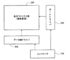
図1は、有機EL素子を用いた表示装置の一般的な構成を示すブロック図である。この表示装置は、表示マトリクス部120と、ゲートドライバ130と、データ線ドライバ140とを有している。表示マトリクス部120は、マトリクス状に配列された複数の画素回路110を有しており、各画素回路110には有機EL素子114がそれぞれ設けられている。画素回路110のマトリクスには、その列方向に沿って伸びる複数のデータ線X1,X2…と、行方向に沿って伸びる複数のゲート線Y1,Y2…とがそれぞれ接続されている。
【0004】
【発明が解決しようとする課題】
図1のような構成で大型表示パネルを構成する場合には、各データ線の静電容量Cdがかなり大きくなる。データ線の静電容量Cdが大きくなるとデータ線の駆動に多大な時間を要する。そのため、従来は、有機EL素子を用いて大型表示パネルを構成するのに十分高速な駆動を行うことができないという問題があった。
【0005】
なお、上述の問題は、有機EL素子を用いた表示装置に限らず、有機EL素子以外の電流駆動型発光素子を用いた表示装置や電気光学装置に共通する問題であった。また、発光素子に限らず、一般に、電流で駆動される電流駆動素子を用いた電子装置に共通する問題であった。
【0006】
本発明は、上述した従来の課題を解決するためになされたものであり、単位回路に接続されたデータ線の駆動時間を短縮することのできる技術を提供することを目的とする。
【0007】
【課題を解決するための手段およびその作用・効果】
上記目的を達成するために、本発明による第1の電気光学装置は、アクティブマトリクス駆動法によって駆動される電気光学装置であって、発光素子と前記発光素子の発光の階調を調節するための回路とをそれぞれ含む複数の単位回路がマトリクス状に配列された単位回路マトリクスと、前記単位回路マトリクスの行方向に沿って配列された単位回路群にそれぞれ接続された複数の走査線と、前記単位回路マトリクスの列方向に沿って配列された単位回路群にそれぞれ接続された複数のデータ線と、前記複数の走査線に接続され、前記単位回路マトリクスの1つの行を選択するための走査線駆動回路と、前記発光素子の発光の階調に応じたデータ信号を生成して、前記複数のデータ線のうちの少なくとも1つのデータ線上に出力することが可能なデータ信号生成回路と、前記走査線駆動回路によって選択された行に存在する少なくとも1つの単位回路に前記データ線を介して前記データ信号が供給される際に、前記データ線の充電または放電を加速することが可能な充放電加速部と、を備え、前記充放電加速部は、前記複数のデータ線をプリチャージすることが可能であり、プリチャージ電圧を任意に設定可能なプリチャージ回路を含む。
【0008】
この電気光学装置では、充放電加速部がデータ線の充電または放電を加速するので、データ信号のみでデータ線の充電または放電が行われる場合に比べて充電または放電に要する時間を短縮することができる。従って、単位回路に接続されたデータ線の駆動時間を短縮することが可能である。
【0009】
なお、前記単位回路による前記発光階調の調節は、前記データ信号の電流値に応じて行われるものであることが好ましい。この場合には、データ信号の電流値が小さいときには、データ線の充電または放電に多大の時間を要する可能性がある。従って、特にデータ信号の電流値が小さいときに、充放電加速部によるデータ線の駆動時間の短縮効果が顕著である。
【0010】
また、前記発光素子は、流れる電流値に応じて発光の階調が変化する電流駆動型の素子であるとしてもよい。また、前記単位回路は、前記発光素子に流れる電流の経路に設けられた駆動トランジスタと、前記駆動トランジスタの制御電極に接続され、前記駆動トランジスタの動作状態に応じた電荷量を保持することによって、前記発光素子に流れる電流値を設定するための保持キャパシタと、を有していてもよい。このとき、前記保持キャパシタの蓄積電荷量が前記データ信号によって調整されるようにしてもよい。この構成では、保持キャパシタの蓄積電荷量を、発光階調に応じた適切な値に設定する必要がある。このとき、充放電加速部によってデータ線の充電または放電を加速するようにすれば、適切な蓄積電荷量を比較的短時間で達成することができ、データ線の駆動を時間短縮することが可能である。
【0011】
前記単位回路は、さらに、前記データ線と前記保持キャパシタとに接続され、前記データ信号によって前記保持キャパシタの蓄積電荷量を調整する際に使用される第1のスイッチングトランジスタと、前記駆動トランジスタおよび前記発光素子と直列に接続された第2のスイッチングトランジスタと、を有していてもよい。また、各走査線は、前記第1と第2のスイッチングトランジスタのそれぞれに接続された第1と第2のサブ走査線を含んでいてもよい。このとき、前記走査線駆動回路は、(i)所定の第1の期間において、前記第1のスイッチングトランジスタをオン状態に設定して、前記保持キャパシタの蓄積電荷量の調整を行う第1の動作と、(ii)前記第1の期間の後の第2の期間において、前記第1のスイッチングトランジスタをオフ状態に設定するとともに前記第2のスイッチングトランジスタをオン状態に設定して、前記発光素子に発光を行わせる第2の動作と、を実行するものとしてもよい。
【0013】
なお、前記プリチャージ回路は、前記第2の期間以外の期間であって前記第1の期間が完了する前の特定のプリチャージ期間において前記プリチャージを実行するものとしてもよい。この構成によれば、保持キャパシタへの電荷の蓄積が完了する前にプリチャージが行われるので、プリチャージが原因となって保持キャパシタの蓄積電荷量が所望の値からずれることを防止することができる。
【0014】
前記プリチャージ期間は、前記第1の期間が開始される以前に設定されることが好ましい。この構成では、プリチャージが保持キャパシタの蓄積電荷量に与える影響をより小さく抑えることが可能である。
【0015】
あるいは、前記プリチャージ期間は、前記第1の期間の初期の一部を含む期間に設定されるようにしてもよい。この構成によれば、データ線の静電容量に比べて保持キャパシタの静電容量が無視できない場合に、保持キャパシタへの電荷の蓄積に要する時間を短縮することができる。
【0016】
前記プリチャージ回路は、前記データ線をプリチャージすることにより、前記データ線を発光階調の中央値以下の低い階調範囲に相当する電圧とすることが好ましい。この構成によれば、発光階調が低く、データ信号によるデータ線の充電または放電に時間が掛かる場合にも、その時間を短縮することができる。
【0017】
なお、前記プリチャージ回路は、前記データ線をプリチャージすることにより、前記データ線をゼロでない最も低い発光階調の近傍の階調に相当する電圧とすることが好ましい。この構成によれば、データ線の充電/放電時間の短縮効果が最も顕著である。
【0018】
各単位回路は、複数の色成分毎にそれぞれ設けられている場合に、前記プリチャージ回路は、各色成分毎に異なる電位で前記データ線を充電または放電することが可能であることが好ましい。この構成によれば、各色成分に適した電位にそれぞれデータ線を充電または放電できるので、データ線の駆動時間をより短縮することが可能である。
【0019】
本発明による他の電気光学装置は、アクティブマトリクス駆動法によって駆動される電気光学装置であって、発光素子と前記発光素子の発光の階調を調節するための回路とをそれぞれ含む複数の単位回路がマトリクス状に配列された単位回路マトリクスと、前記単位回路マトリクスの行方向に沿って配列された単位回路群にそれぞれ接続された複数の走査線と、前記単位回路マトリクスの列方向に沿って配列された単位回路群にそれぞれ接続された複数のデータ線と、前記複数の走査線に接続され、前記単位回路マトリクスの1つの行を選択するための走査線駆動回路と、前記発光素子の発光の階調に応じたデータ信号を生成して、前記複数のデータ線のうちの少なくとも1つのデータ線上に出力することが可能なデータ信号生成回路と、前記走査線駆動回路によって選択された行に存在する少なくとも1つの単位回路に前記データ線を介して前記データ信号が供給される際に、前記データ線の充電または放電を加速することが可能な充放電加速部と、を備える。前記充放電加速部は、前記各発光素子の発光の階調に応じたデータ信号の電流値に、前記データ線の充電または放電を加速するための電流値を付加する付加電流回路を含み、前記付加電流回路は、外部からの制御により前記付加電流の電流値を複数のレベルに切り換え可能な回路を含む。この構成によっても、データ線の充電または放電を容易に促進することができる。
【0020】
前記電流値の付加は、前記各発光素子の発光の階調に応じたデータ信号が生成される期間の初期に実行されるものとしてもよい。こうすれば、電流値の付加による発光素子の発光階調への影響を小さく抑えることができる。
【0021】
前記付加電流回路は、各データ線に対して前記データ信号生成回路と並列に接続されたトランジスタを含むものとしてもよい。この構成によれば、付加電流を容易に発生することができる。
【0022】
本発明による電気光学装置の第1の駆動方法は、発光素子と前記発光素子の発光の階調を調節するための回路とをそれぞれ含む複数の単位回路がマトリクス状に配列された単位回路マトリクスと、各発光素子の発光の階調に応じたデータ信号を各単位回路に供給するための複数のデータ線と、を備えたアクティブマトリクス駆動型の電気光学装置の駆動方法であって、少なくとも1つの単位回路に前記データ線を介して前記データ信号を供給する際に、所定のプリチャージ期間において前記データ線をプリチャージすることによって前記データ線の充電または放電を加速し、前記プリチャージは、プリチャージ電圧を任意に設定可能なプリチャージ回路によって行われることを特徴とする。
【0023】
また、本発明による電子装置は、流れる電流値に応じて動作が制御される複数の電流駆動素子と、各電流駆動素子に、前記電流駆動素子の動作状態を規定するデータ信号を供給するためのデータ線と、前記データ線上に前記データ信号を出力するためのデータ信号生成回路と、前記データ線を介して前記データ信号が前記電流駆動素子に供給される際に、前記データ線の充電または放電を加速するための充放電加速部と、を備え、前記充放電加速部は、前記複数のデータ線をプリチャージすることが可能であり、プリチャージ電圧を任意に設定可能なプリチャージ回路を含む。
【0024】
本発明による第2の電気光学装置は、入力信号に対応して電流を生成する電流生成回路と、電気光学素子を備えた単位回路と、前記電流を前記単位回路に供給するデータ線と、を含む電気光学装置であって、前記入力信号の変化に伴う前記電流の変化を加速する加速手段と、前記入力信号の変化に伴う前記電流の変化量に基づいて、前記加速手段の使用の要否を判断する判断回路と、を備えることを特徴とする。
【0025】
この電気光学装置によれば、入力信号の変化に伴って電流を変化させる際に、加速手段が入力信号の変化に伴う電流の変化を加速する加速操作を行うので、入力信号に応じて速やかに電流値を変更することができる。従って、単位回路に接続されたデータ線の駆動時間を短縮することが可能である。
【0026】
なお、前記加速手段は、前記データ線の電位を、所定の電位に設定するプリチャージ回路であるものとしてもよい。
【0027】
あるいは、前記加速手段は、前記データ線に流れる電流の一部の電流経路となる付加電流回路であるものとしてもい。
【0029】
本発明による電気光学装置の第2の駆動方法は、入力信号に対応して電流を生成する電流生成回路と、電気光学素子を備えた単位回路と、前記電流を前記単位回路に供給するデータ線と、を含む電気光学装置の駆動方法であって、前記入力信号の変化に伴い前記電流の電流値を第1の電流値から第2の電流値に変化させる操作を、電流値の時間変化率の異なる複数の期間を経て行うことを特徴とする。
【0030】
この構成によれば、入力信号の変化に伴って電流を変化させる際に、第1の電流値から第2の電流値に変化させる操作を、時間変化率の異なる複数の期間を経て行うようにしたので、第1の電流値から第2の電流値に変化するまでに要する所要時間の短縮を図ることができる。従って、単位回路に接続されたデータ線の駆動時間を短縮することが可能である。
【0031】
本発明による第3の電気光学装置は、入力信号に対応して電流を生成する電流生成回路と、電気光学素子を備えた単位回路と、前記電流を前記単位回路に供給するデータ線と、を含む電気光学装置であって、前記入力信号の変化に対応して前記電流を変化させる際に、前記データ線の電荷をリセットするリセット手段を備えることを特徴とする。
【0032】
この電気光学装置によれば、入力信号の変化に対応して電流を変化させる際に、リセット手段によってデータ線の電荷をリセットするようにしたので、データ線の電流値をより速やかに変化させることができる。従って、単位回路に接続されたデータ線の駆動時間を短縮することが可能である。
【0033】
前記単位回路は、前記電流に応じた電圧を保持する電圧保持手段を備え、 前記リセット手段は、前記データ線及び前記電圧保持手段の電荷をリセットするようになっていてもよい。この構成によれば、データ線及び電圧保持手段の電荷を共にリセットするようにしたので、データ線だけでなく、電圧保持手段の保持電圧も、変化後の電流値に応じた保持電圧により速やかに一致させることができる。
【0034】
本発明による第2の電子装置は、入力信号に対応して電流を生成する電流生成回路と、電流駆動素子を備えた単位回路と、前記電流を前記単位回路に供給するデータ線と、を含む電子装置であって、前記入力信号の変化に伴う前記電流の変化を加速する加速手段を備えることを特徴とする。
【0035】
なお、本発明は、種々の形態で実現することが可能であり、例えば、電気光学装置、表示装置、その電気光学装置や表示装置を備えた電子装置、それらの装置の駆動方法、その方法の機能を実現するためのコンピュータプログラム、そのコンピュータプログラムを記録した記録媒体、そのコンピュータプログラムを含み搬送波内に具現化されたデータ信号、等の形態で実現することができる。
【0036】
【発明の実施の形態】
次に、本発明の実施の形態を実施例に基づいて以下の順序で説明する。
A.第1実施例(付加電流その1):
B.第2実施例(付加電流その2):
C.第3実施例(付加電流その3):
D.付加電流を利用した変形例:
E.第4実施例(プリチャージ):
F.プリチャージタイミングに関する変形例:
G.プリチャージ回路の配置に関する変形例:
H.電子機器への適用例:
I.その他の変形例:
【0037】
A.第1実施例(付加電流その1):
図2は、本発明の第1実施例としての表示装置の概略構成を示すブロック図である。この表示装置は、コントローラ100と、表示マトリクス部200(「画素領域」とも呼ぶ)と、ゲートドライバ300と、データ線ドライバ400とを有している。コントローラ100は、表示マトリクス部200に表示を行わせるためのゲート線駆動信号とデータ線駆動信号を生成して、ゲートドライバ300とデータ線ドライバ400にそれぞれ供給する。
【0038】
図3は、表示マトリクス部200とデータ線ドライバ400の内部構成を示している。表示マトリクス部200は、マトリクス状に配列された複数の画素回路210を有しており、各画素回路210は有機EL素子220をそれぞれ有している。画素回路210のマトリクスには、その列方向に沿って伸びる複数のデータ線Xm(m=1〜M)と、行方向に沿って伸びる複数のゲート線Yn(n=1〜N)とがそれぞれ接続されている。なお、データ線は「ソース線」とも呼ばれ、また、ゲート線は「走査線」とも呼ばれる。また、本明細書では、画素回路210を「単位回路」あるいは「画素」とも呼ぶ。画素回路210内のトランジスタは、通常はTFTで構成される。
【0039】
ゲートドライバ300は、複数のゲート線Ynの中の1本を選択的に駆動して1行分の画素回路群を選択する。データ線ドライバ400は、各データ線Xmをそれぞれ駆動するための複数の単一ラインドライバ410を有している。これらの単一ラインドライバ410は、各データ線Xmを介して画素回路210にデータ信号を供給する。このデータ信号に応じて画素回路210の内部状態(後述する)が設定されると、これに応じて有機EL素子220に流れる電流値が制御され、この結果、有機EL素子220の発光の階調が制御される。
【0040】
コントローラ100(図2)は、画素領域200の表示状態を表す表示データ(画像データ)を、各有機EL素子220の発光の階調を表すマトリクスデータに変換する。マトリクスデータは、1行分の画素回路群を順次選択するためのゲート線駆動信号と、選択された画素回路群の有機EL素子220に供給するデータ線信号のレベルを示すデータ線駆動信号とを含んでいる。ゲート線駆動信号とデータ線駆動信号は、ゲートドライバ300とデータ線ドライバ400にそれぞれ供給される。コントローラ100は、また、ゲート線とデータ線の駆動タイミングのタイミング制御を行う。
【0041】
図4は、画素回路210の内部構成を示す回路図である。この画素回路210は、m番目のデータ線とn番目のゲート線Ynとの交点に配置されている回路である。なお、ゲート線Ynは、2本のサブゲート線V1,V2を含んでいる。
【0042】
画素回路210は、データ線Xmに流れる電流値に応じて有機EL素子220の階調を調節する電流プログラム回路である。具体的には、この画素回路210は、有機EL素子220の他に、4つのトランジスタ211〜214と、保持キャパシタ230(「保持コンデンサ」あるいは「記憶キャパシタ」とも呼ぶ)とを有している。保持キャパシタ230は、データ線Xmを介して供給されたデータ信号に応じた電荷を保持し、これによって、有機EL素子220の発光の階調を調節するためのものである。すなわち、保持キャパシタ230は、データ線Xmに流れる電流に応じた電圧を保持する電圧保持手段に相当する。第1ないし第3のトランジスタ211〜213はnチャンネル型FETであり、第4のトランジスタ214はpチャンネル型FETである。有機EL素子220は、フォトダイオードと同様の電流注入型(電流駆動型)の発光素子なので、ここではダイオードの記号で描かれている。
【0043】
第1のトランジスタ211のソースは、第2のトランジスタ212のドレインと、第3のトランジスタ213のドレインと、第4のトランジスタ214のドレインと、にそれぞれ接続されている。第1のトランジスタ211のドレインは、第4のトランジスタ214のゲートに接続されている。保持キャパシタ230は、第4のトランジスタ214のソースとゲートとの間に接続されている。また、第4のトランジスタ214のソースは、電源電位Vddにも接続されている。
【0044】
第2のトランジスタ212のソースは、データ線Xmを介して単一ラインドライバ410(図3)に接続されている。有機EL素子220は、第3のトランジスタ213のソースと接地電位との間に接続されている。
【0045】
第1と第2のトランジスタ211,212のゲートは、第1のサブゲート線V1に共通に接続されている。また、第3のトランジスタ213のゲートは、第2のサブゲート線V2に接続されている。
【0046】
第1と第2のトランジスタ211,212は、保持キャパシタ230に電荷を蓄積する際に使用されるスイッチングトランジスタである。第3のトランジスタ213は、有機EL素子220の発光期間においてオン状態に保たれるスイッチングトランジスタである。また、第4のトランジスタ214は、有機EL素子220に流れる電流値を制御するための駆動トランジスタである。第4のトランジスタ214の電流値は、保持キャパシタ230に保持される電荷量(蓄積電荷量)によって制御される。
【0047】
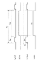
図5は、画素回路210の通常の動作を示すタイミングチャートである。ここでは、第1のサブゲート線V1の電圧値(以下、「第1のゲート信号V1」も呼ぶ)と、第2のサブゲート線V2の電圧値(以下、「第2のゲート信号V2」も呼ぶ)と、データ線Xmの電流値Iout (「データ信号Iout 」も呼ぶ)と、有機EL素子220に流れる電流値IELとが示されている。
【0048】
駆動周期Tcは、プログラミング期間Tprと発光期間Telとに分かれている。ここで、「駆動周期Tc」とは、表示マトリクス部200内のすべての有機EL素子220の発光の階調が1回ずつ更新される周期を意味しており、いわゆるフレーム周期と同じものである。階調の更新は、1行分の画素回路群毎に行われ、駆動周期Tcの間にN行分の画素回路群の階調が順次更新される。例えば、30Hzで全画素回路の階調が更新される場合には、駆動周期Tcは約33msである。
【0049】
プログラミング期間Tprは、有機EL素子220の発光の階調を画素回路210内に設定する期間である。本明細書では、画素回路210への階調の設定を「プログラミング」と呼んでいる。例えば、駆動周期Tcが約33msであり、ゲート線Ynの総数Nが480本である場合には、プログラミング周期Tprは約69μs(=33ms/480)以下になる。
【0050】
プログラミング期間Tprでは、まず、第2のゲート信号V2をLレベルに設定して第3のトランジスタ213をオフ状態(閉状態)に保つ。次に、データ線Xm上に発光階調に応じた電流値Imを流しながら、第1のゲート信号V1をHレベルに設定して第1と第2のトランジスタ211,212をオン状態(開状態)にする。このとき、このデータ線Xmの単一ラインドライバ410(図4)は、発光階調に応じた一定の電流値Imを流す定電流源として機能する。図5(c)に示されているように、この電流値Imは、所定の電流値の範囲RI内において、有機EL素子220の発光の階調に応じた値に設定されている。
【0051】
保持キャパシタ230には、第4のトランジスタ214(駆動トランジスタ)を流れる電流値Imに対応した電荷を保持した状態となる。この結果、第4のトランジスタ214のソース/ゲート間には、保持キャパシタ230に記憶された電圧が印加される。なお、本明細書では、プログラミングに用いられるデータ信号の電流値Imを「プログラミング電流値Im」と呼ぶ。
【0052】
プログラミングが終了すると、ゲートドライバ300が第1のゲート信号V1をLレベルに設定して第1と第2のトランジスタ211,212をオフ状態とし、また、データ線ドライバ400はデータ信号Iout を停止する。
【0053】
発光期間Telでは、第1のゲート信号V1をLレベルに維持して第1と第2のトランジスタ211,212をオフ状態に保ったまま、第2のゲート信号V2をHレベルに設定して第3のトランジスタ213をオン状態に設定する。保持キャパシタ230には、プログラミング電流値Imに対応した電圧が予め記憶されているので、第4のトランジスタ214にはプログラミング電流値Imとほぼ同じ電流が流れる。従って、有機EL素子220にもプログラミング電流値Imとほぼ同じ電流が流れ、この電流値Imに応じた階調で発光する。このように、保持キャパシタ230の電圧(すなわち電荷)が電流値Imによって書き込まれるタイプの画素回路210は、「電流プログラム回路」と呼ばれている。
【0054】
図6は、単一ラインドライバ410の内部構成を示す回路図である。単一ラインドライバ410は、データ信号生成回路420(「制御電流発生部」あるいは「電流生成回路」とも呼ぶ)と、付加電流回路430(「付加電流発生部」とも呼ぶ)とを備えている。データ信号生成回路420と付加電流回路430は、データ線Xmと接地電位との間に並列に接続されている。
【0055】
データ信号生成回路420は、スイッチングトランジスタ41と駆動トランジスタ42との直列接続421が、N組分(Nは2以上の整数)並列に接続された構成を有している。図6の例ではNは6である。6つの駆動トランジスタ42のゲートには、リファレンス電圧Vref1が共通に印加されている。また、6つの駆動トランジスタ42の利得係数βの比は、1:2:4:8:16:32に設定されている。なお、利得係数βは、良く知られているように、β=(μC0 W/L)で定義される。ここで、μはキャリアの移動度、C0 はゲート容量、Wはチャンネル幅、Lはチャンネル長である。6つの駆動トランジスタ42は、定電流源として機能する。トランジスタの電流駆動能力は利得係数βに比例するので、6つの駆動トランジスタ42の電流駆動能力の比は、1:2:4:8:16:32である。
【0056】
6つのスイッチングトランジスタ41のオン/オフは、コントローラ100(図2)から与えられる6ビットのデータ線駆動信号Ddata(「入力信号」とも呼ぶ)によって制御される。データ線駆動信号Ddataの最下位ビットは、利得係数βが最も小さな(すなわちβの相対値が1の)直列接続421に供給されており、最上位ビットは利得係数βが最も小大きな(すなわちβの相対値が32の)直列接続421に供給されている。この結果、データ信号生成回路420は、データ線駆動信号Ddataの値に比例した電流値Imを生成する電流源として機能する。データ線駆動信号Ddataの値は、有機EL素子220の発光の階調を示す値に設定されている。従って、データ信号生成回路420からは、有機EL素子220の発光の階調に応じた電流値Imを有するデータ信号が出力される。
【0057】
付加電流回路430は、スイッチングトランジスタ43と駆動トランジスタ44との直列接続で構成されている。駆動トランジスタ44のゲート電極には、リファレンス電圧Vref2が印加される。スイッチングトランジスタ43のオン/オフは、コントローラ100から与えられる付加電流制御信号Dpによって制御される。スイッチングトランジスタ43がオン状態のときには、リファレンス電圧Vref2に応じた所定の付加電流Ipが付加電流回路430からデータ線Xm上に出力される。
【0058】
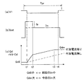
図7は、付加電流回路430を利用した場合のプログラミング期間Tpr(図5)における電流値の変化を示す説明図である。時点t1では、データ信号生成回路420からプログラミング電流Imの出力が開始され、また、付加電流回路430からも付加電流Ipの出力が開始される。このとき、単一ラインドライバ410から出力される電流値Iout は、プログラミング電流Imと付加電流Ipの和(Im+Ip)になる。時点t2で付加電流Ipが停止した後の期間t2〜t4では、プログラミング電流Imだけが単一ラインドライバ410の出力電流となる。なお、付加電流Ipが流れる期間t1〜t2は、例えば、プログラミング電流Imが流れる期間t1〜t4の初期の1/4程度の期間に設定される。付加電流Ipが流れる期間t1〜t2をプログラミング電流Imが流れる期間の初期に設定するのは、付加電流Ipによる発光階調への影響を小さく抑えるためである。なお、付加電流Ipの値は、例えばプログラミング電流Imの最大値と最小値の中間値程度の値に設定される。
【0059】
正確に言えば、図7(a)に示す出力電流Iout は単一ラインドライバ410の電流駆動能力を示しており、データ線Xm上の実電流値Isは、図7(b)に実線で示すように変化する。すなわち、時点t1では、過渡的に大きな電流が流れるが、徐々に減少して、電流値(Im+Ip)に近づいてゆく。時点t2で付加電流回路430がオフになると、実電流Isはさらに減少する。しかし、時点t2以降では、電流値自体が小さいのでデータ線容量Cd(図3)を充電または放電する速度が低下し、この結果、電流値の変化はt1〜t2の期間よりも緩やかになる。そして、時点t3では、プログラミング電流値Imにまで実電流値Isが減少し、期間t3〜t4ではこのプログラミング電流値Imが維持される。従って、プログラミング期間Tpr内において、正しいプログラミング電流値Imで画素回路210がプログラミングされる。
【0060】
このような付加電流Ipの利用は、「プログラミング電流値Imを、前回の行のプログラミング時における第1の電流値から、今回の行のプログラミング時における第2の電流値に変化させる操作を、電流値の時間変化率が異なる複数の期間(図7の期間t1〜t2と、期間t2〜t3)を経て行うもの」と考えることも可能である。なお、この第1の電流値から第2の電流値への変化は、今回のプログラミング時のプログラミング電流Imと付加電流Ipとの和である第3の電流値(Im+Ip)を経由して行われる。
【0061】
図7(b)に示す一点破線は、付加電流Ipを用いずに、単一ラインドライバ410の電流駆動能力が一定である場合(図7(c))の実電流値の変化を示している。このときには、付加電流Ipを用いる場合に比べて期間t1〜t2における電流値が小さいので、電流の変化もより緩やかである。従って、プログラミングの終了時点t4においても、実電流値Isがプログラミング電流値Imに達しない場合がある。このような場合には、画素回路210を正しい階調にプログラミングすることができない可能性がある。あるいは、正しくプログラミングを行うために、プログラミング期間Tprを延長しておく必要が生じるという問題を生じる。これに対して、付加電流Ipを用いると、プログラミング期間Tpr内に正しくプログラミングを行うことが可能である。
【0062】
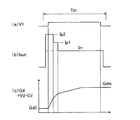
図8は、プログラミング期間Tprにおけるデータ線Xmの電荷量Qdの変化を示す説明図である。図8は、図7の動作を電荷量の観点で描いたものである。なお、図7における時点t1,t4は、正確に言えば、図8に示されているように、第1のゲート信号V1のレベルが変化する時点に相当する。
【0063】
一般に、n番目の行の画素回路群のプログラミングが開始される前は、データ線Xmの容量値Qc0は、(n−1)番目の行の画素回路群のプログラミングにおけるデータ線Xmのプログラミング電流値Imに依存している。図9は、有機EL素子の発光の階調Gと、データ線Xmの電流値Im(すなわちプログラミング電流値)と、データ線の電荷量Qdとの関係を示している。第1実施例の回路構成では、階調Gが高いほど(すなわち輝度が高いほど)電流Imは増大し、データ線の電荷量Qd(すなわち電圧Vd)は低下する傾向にある。電荷量Qdは、最も低い階調Gmin では電源電圧Vddに近い電圧に相当する電荷量となり、最も高い階調Gmax では接地電位に近い電圧に相当する電荷量となる。なお、図8(c)の例では、直前の行(すなわち(n−1)番目の行)のプログラミングにおけるプログラミング電流値Imが比較的大きく、従って、今回のプログラミング開始前の電荷量Qd0が比較的小さい場合を想定している。
【0064】
図8の時点t1でプログラミングが開始されると、データ線Xmは単一ラインドライバ410の出力電流Iout (=Im+Ip)によって充電または放電され、電荷量Qdは比較的速い速度で増大する。時点t2で付加電流Ipが無くなると充電/放電速度が低下し、電荷量Qdの変化もより緩やかになる。しかし、プログラミング期間Tpr内の時点t3において、所望のプログラミング電流値Imに対応する電荷量Qdmに到達している。
【0065】
以上の説明から理解できるように、付加電流回路430は、データ線Xmの充電または放電を加速するための充放電加速部として機能する。なお、本明細書において、「充電または放電の加速」とは、本来の望ましい電流値(本実施例ではプログラミング電流値Im)のみによるデータ線の充電または放電よりも短時間で充電または放電が終了するように、充電または放電を促進する操作を意味する。また、付加電流回路430は、データ信号の変化に伴う電流の変化を加速する加速手段、あるいは、データ線Xmの電荷量を所定の値にリセットするためのリセット手段として機能すると考えることも可能である。
【0066】
図8(c)に一点鎖線で示すように、付加電流Ipが無い場合には充電/放電速度は低い速度に保たれており、この例では、プログラミング期間Tprの終期t4においても所望のプログラミング電流値Imに対応する電荷量Qdmに到達していない。従って、画素回路210に正しいプログラミング電流Imを供給して正しい階調にプログラミングすることができない可能性がある。
【0067】
このように、本実施例においては、付加電流Ipを用いてデータ線の充電または放電を加速を行うことにより、画素回路210に対して正しいプログラミングを行うことが可能である。また、プログラミング時間を短縮して、有機EL素子220の駆動制御の高速化を図ることができる。
【0068】
なお、付加電流Ipを用いたデータ線の充電または放電の加速は、通常は、画素回路マトリクスに含まれるすべてのデータ線Xmについて同時に行われる。但し、画素回路マトリクスに含まれる複数のデータ線の中の一部のデータ線に対してのみ、付加電流Ipを用いたデータ線の充電または放電の加速を選択的に行うようにしてもよい。例えば、プログラミングの開始時におけるm番目のデータ線Xmの電荷量Qd0(図8)が、所望のプログラミング電流Imに対応する電荷量Qdmに十分に近い場合には、付加電流Ipを利用しなくてもよい。具体的には、コントローラ100が、各データ線に関して、(n−1)番目の行でのプログラミング電流値とn番目の行でのプログラミング電流値とを互いに比較し、その差が所定の閾値以内であれば、n番目の行のプログラミング時に付加電流Ipを利用しないことと判断してもよい。また、これらのプログラミング電流値の差に応じて、付加電流Ipの値を変化させてもよい。換言すれば、プログラミング電流値Imの前回値と今回値との差に応じて付加電流Ipの電流値を決定する手段と、決定された付加電流値Ipを各データ線Xmに供給する手段とを設けるようにしてもよい。この構成によれば、より効果的に付加電流値Ipを利用することができ、駆動の高速化を促進することができる。
【0069】
あるいは、今回のプログラミング電流値Imが所定の閾値よりも小さい場合にのみ付加電流Ipを利用し、プログラミング電流値Imが閾値よりも大きい場合には付加電流Ipを利用しないことと判断しても良い。この理由は、プログラミング電流値Imが大きい場合には、データ線Xmの充電または放電が十分に早く行われるので、付加電流Ipを利用しなくても十分高速に所望のプログラミング電流値Imを達成できるからである。
【0070】
この代わりに、今回のプログラミング電流値(第2の電流値)が前回のプログラミング電流値(第1の電流値)よりも小さく、且つ、今回のプログラミング電流値Imと付加電流値Ipとの和(第3の電流値)が、前回のプログラミング電流値よりも小さいときにのみ、付加電流Ipを利用することとしてもよい。これらの3つの電流値は、これ以外の種々の関係に設定することも可能である。例えば、第3の電流値を、第1の電流値と第2の電流値との間の電流値であるとしてもよい。また、第1の電流値から第3の電流値への電流値の時間変化率の絶対値を、第3の電流値から第2の電流値への電流値の時間変化率の絶対値よりも大きいものとしてもよい。さらに、第1の電流値と第3の電流値との差の絶対値を、第3の電流値と第2の電流値との差の絶対値よりも大きいものとしてもよい。
【0071】
付加電流Ipを利用するか否かの判断は、各データ線毎に行うことが好ましい。但し、直前の行のプログラミング時におけるプログラミング電流の値に拘わらず、常に付加電流Ipを利用するものとすれば、表示装置全体の制御が単純になるという利点がある。
【0072】
以上のように、本実施例では、プログラミング期間の初期に付加電流Ipをプログラミング電流Imに加算することによって、短時間で正確なプログラミングを行うことが可能である。あるいは、プログラミング時間を短縮して、有機EL素子220の駆動制御の高速化を図ることが可能である。特に、表示パネルの大型化や高解像度化に伴って駆動制御の高速化が要求されるので、大型表示パネルや高解像度表示パネルにおいて上述の効果が顕著である。
【0073】
B.第2実施例(付加電流その2):
図10は、本発明の第2実施例としての表示装置の概略構成を示すブロック図である。この表示装置は、データ線ドライバ400aが電源電位Vdd側に設けられている点が第1実施例と異なる。また、以下に説明するように、単一ラインドライバ410aの内部構成と、画素回路210aの内部構成も第1実施例と異なっている。
【0074】
図11は、画素回路210aの内部構成を示す回路図である。この画素回路210aは、いわゆるサーノフ型の電流プログラム回路である。この画素回路210aは、有機EL素子220と、4つのトランジスタ241〜244と、保持キャパシタ230とを有している。なお、4つのトランジスタ241〜244は、pチャンネル型FETである。
【0075】
データ線Xmには、第1のトランジスタ241と、保持キャパシタ230と、第2のトランジスタ242とがこの順に直列に接続されている。第2のトランジスタ242のドレインは、有機EL素子220に接続されている。第1と第2のトランジスタ241,242のゲートには、第1のサブゲート線V1が共通に接続されている。
【0076】
電源電位Vddと接地電位との間には、第3のトランジスタ243と、第4のトランジスタ244と、有機EL素子220との直列接続が介挿されている。第3のトランジスタ243のドレインと第4のトランジスタ244のソースは、第1のトランジスタのドレインにも接続されている。第3のトランジスタ243のゲートには、第2のゲート線V2が接続されている。また、第4のトランジスタ244のゲートは、第2のトランジスタ242のソースに接続されている。保持キャパシタ230は、第4のトランジスタ244のソースとゲートとの間に接続されている。
【0077】
第1と第2のトランジスタ241,242は、保持キャパシタ230に所望の電荷を蓄積する際に使用されるスイッチングトランジスタである。第3のトランジスタ243は、有機EL素子220の発光期間においてオン状態に保たれるスイッチングトランジスタである。また、第4のトランジスタ244は、有機EL素子220に流れる電流値を制御するための駆動トランジスタである。第4のトランジスタ244の電流値は、保持キャパシタ230に保持される電荷量によって制御される。
【0078】
図12は、第2実施例の画素回路210aの通常の動作を示すタイミングチャートである。この動作では、図5に示した第1実施例の動作から、ゲート信号V1,V2の論理が反転している。また、第2実施例では、図11の回路構成から理解できるように、プログラミング期間Tprにおいて、第1と第4のトランジスタ241,244を経由して有機EL素子220にプログラミング電流Imが流れる。従って、第2実施例では、プログラミング期間Tprにおいても有機EL素子220が発光する。このように、プログラミング期間Tprでは、有機EL素子220が発光しても良く、あるいは、第1実施例のように発光しなくてもよい。
【0079】
図13は、第2実施例の単一ラインドライバ410aを示す回路図である。この単一ラインドライバ410aは、データ線Xmの電源電位Vdd側に接続されている。このため、データ信号生成回路420aの駆動トランジスタ42と、付加電流回路430aの駆動トランジスタ44とが、いずれもpチャンネル型FETで構成されている点で図6に示した第1実施例と異なっている。他の構成は、第1実施例と同じである。
【0080】
図14は、第2実施例における有機EL素子の発光の階調Gと、データ線Xmの電流値Imと、データ線の電荷量Qdとの関係を示している。第2実施例では、第1実施例とは反対に、単一ラインドライバ410aがデータ線Xmの電源電位Vdd側に設けられているので、階調Gとデータ線Xmの電荷量Qd(すなわち電圧Vd)との関係が第1実施例とは逆転している。すなわち、階調Gが高いほど(すなわち輝度が高いほど)、データ線の電荷量Qd(すなわち電圧Vd)は上昇する傾向にある。電荷量Qdは、最も低い階調Gmin では接地電圧に近い電圧に相当する電荷量となり、最も高い階調Gmax では電源電位Vddに近い電圧に相当する電荷量となる。
【0081】
図15は、第2実施例でのプログラミング期間Tprにおけるデータ線Xmの電荷量Qdの変化を示す説明図である。この変化は、図8に示した第1実施例での変化と本質的には同じである。但し、図15(c)においてプログラミング開始前の電荷量Qd0が比較的小さいことは、第1実施例とは逆に、直前の行(すなわち(n−1)番目の行)のプログラミングにおけるプログラミング電流値Imが比較的小さいことを意味している。
【0082】
この第2実施例の表示装置も、第1実施例と同様の効果を有する。すなわち、プログラミング期間Tprの初期に付加電流Ipをプログラミング電流Imに加算することによって、画素回路210aに対して短時間で正確なプログラミングを行うことが可能である。あるいは、プログラミング時間を短縮して、有機EL素子220の駆動制御の高速化を図ることが可能である。
【0083】
C.第3実施例(付加電流その3):
図16は、第3実施例の単一ラインドライバ回路410bを示す回路図である。この単一ラインドライバ410b内のデータ信号生成回路420は、図6に示した第1実施例と同じであるが、付加電流回路430bの構成が第1実施例と異なっている。すなわち、この付加電流回路430bは、スイッチングトランジスタ43と駆動トランジスタ44との直列接続を2組有しており、これらは互いに並列に接続されている。2つの駆動トランジスタ44の利得係数βcの比は、例えば1:2に設定される。また、付加電流制御信号Dpも2ビットの信号として供給される。この付加電流回路430bを用いた場合には、付加電流値Ipを、付加電流制御信号Dpが取り得る4つの値0〜3に応じた4つのレベルのいずれかに任意に設定することが可能である。
【0084】
図17は、第3実施例の付加電流回路430bを利用した場合のプログラミング期間Tprの動作を示す説明図である。ここでは、付加電流値Ipが、より高い第1のレベルIp2から、より低い第2のレベルIP1に変化している。この結果、第1実施例や第2実施例に比べて、より早くデータ線を充電または放電できる可能性がある。この例からも理解できるように、付加電流を利用する場合に、付加電流値を2段階以上に変化させて、データ線Xmの出力電流Iout を3段階以上に変化させるようにしてもよい。
【0085】
また、図16の付加電流回路430bを用いた場合にも、第1実施例と同様に、付加電流値Ipのレベルを、直前の行に対するプログラミング電流値と、今回の行に対するプログラミング電流値とに応じて決定することが可能である。こうすれば、プログラミング電流値に応じた適切な付加電流値を選択的に利用することが可能である。
【0086】
なお、このような多値の付加電流値Ipを利用した付加電流回路430bは、第2実施例にも適用可能である。
【0087】
D.付加電流を利用した変形例:
付加電流の利用に関しては、以下のような種々の変形が可能である。
【0088】
D1:
付加電流回路は、単一ラインドライバ410の中に設ける必要は無く、データ線Xmに接続されていれば他の位置に設けることも可能である。また、各データ線Xm毎に1つの付加電流回路を設ける代わりに、複数のデータ線に対して1つの付加電流回路を設けてもよい。
【0089】
D2:
また、付加電流回路を設けずに、データ信号生成回路420によってプログラミング電流値Imよりも大きな電流値をプログラミング期間の初期に発生させ、所定時間の経過後にプログラミング電流値Imに切り換えるようにしてもよい。
【0090】
以上の各種の実施例や変形例からも理解できるように、付加電流を利用する際には、一般に、プログラミングの初期においてプログラミング電流値Imよりも大きな電流をデータ線に流すようにすれば良い。こうすることによって、そのデータ線の充電または放電を促進することができ、正確なプログラミングや高速な駆動が可能となる。
【0091】
E.第4実施例(プリチャージ):
図18は、本発明の第4実施例としての表示装置の構成を示すブロック図である。この表示装置は、図3に示した第1実施例の表示装置の各データ線Xm(m=1〜M)に、プリチャージ回路600をそれぞれ設けたものであり、他の構成は図3に示したものと同じである。但し、データ線の静電容量Cdは図示の便宜上省略されている。なお、単一ラインドライバ410としては、付加電流回路430(図6)を有していないものを利用することも可能である。
【0092】
各データ線Xmには、表示マトリクス部200とデータ線ドライバ400との間の位置に、プリチャージ回路600がそれぞれ接続されている。プリチャージ回路600は、定電圧源であるプリチャージ電源Vpと、スイッチングトランジスタ610との直列接続で構成されている。この例では、スイッチングトランジスタ610はnチャンネル型FETであり、そのソースがデータ線Xnに接続されている。各スイッチングトランジスタ610のゲートには、コントローラ100(図2)からプリチャージ制御信号Preが共通に入力されている。プリチャージ電源Vpの電位は、例えば画素回路210の駆動電源電位Vdd(図4)に設定される。但し、プリチャージ電圧Vpを任意に調整できるような電源回路を採用してもよい。
【0093】
プリチャージ回路600は、プログラミングの完了前に各データ線Xmの充電または放電を行って、プログラミングに要する時間を短縮するための回路である。換言すれば、プリチャージ回路600は、データ線Xmの充電または放電を加速するための充放電加速部として機能する。また、プリチャージ回路600は、データ信号の変化に伴う電流の変化を加速する加速手段、あるいは、データ線Xmの電荷量を所定の値にリセットするためのリセット手段として機能すると考えることも可能である。
【0094】
図19は、第4実施例におけるプログラミング期間Tprの動作を示す説明図である。この例では、期間t13〜t15におけるプログラミングの実行の前に、期間t11〜t12においてプリチャージ制御信号PreがHレベルとなり、プリチャージ回路600による充電または放電(プリチャージ)が行われる。このプリチャージによって、データ線Xmの電荷量Qdは、プリチャージ電圧Vp(図18)に応じた所定の値に到達する。換言すれば、データ線Xmがプリチャージ電圧Vpにほぼ等しい電圧まで到達する。その後、期間t13〜t15でプログラミングが実行されると、プログラミング期間Tpr内の時点t14において、データ線Xnの電荷量Qdが所望のプログラミング電流値Imに対応する電荷量Qdmに到達する。
【0095】
図19(d)の一点破線は、プリチャージや付加電流を利用しない場合の電荷量の変化を示している。この場合には、プログラミング期間Tprの終期においても、データ線の電荷量が所望のプログラミング電流値Imに対応する電荷量Qdmに到達していない。従って、画素回路210に正しいプログラミング電流Imを供給して正しい階調にプログラミングすることができない可能性がある。
【0096】
このように、本実施例においては、プリチャージを行ってデータ線の充電または放電を加速することにより、画素回路210に対して正しい発光階調を設定することが可能である。また、プログラミング時間を短縮して、有機EL素子220の駆動制御の高速化を図ることができる。
【0097】
なお、データ線ドライバ400がデータ線Xmの接地電位側に設けられているときには、前述した図9に示されているように、プログラミング電流値Imが小さいほどデータ線の電荷量Qdが多く、その電圧Vdも大きい。この場合には、プリチャージ電圧Vpは、比較的小さなプログラミング電流値Im(すなわち比較的低い発光階調)に相当する比較的高い電圧値に設定することが好ましい。
【0098】
一方、データ線ドライバ400がデータ線Xmの電源電位側に設けられているときには、前述した図14に示されているように、プログラミング電流値Imが小さいほどデータ線の電荷量Qdも少なく、その電圧Vdも小さい。この場合には、プリチャージ電圧Vpは、比較的小さなプログラミング電流値Im(すなわち比較的低い発光階調)に相当する比較的低い電圧値に設定することが好ましい。
【0099】
具体的には、プリチャージ電圧Vpは、発光階調の中央値以下の低い階調範囲に相当する電圧値にデータ線をプリチャージできるように設定されることが好ましい。特に、ゼロでない最も低い発光階調の近傍の階調に相当する電圧値にデータ線をプリチャージできるように、プリチャージ電圧Vpを設定することが好ましい。ここで、「ゼロでない最も低い発光階調の近傍の階調」とは、例えば全階調範囲が0〜255の場合には、階調値が1から10程度の範囲の階調を意味している。こうすれば、プログラミング電流値Imが小さい場合にも、十分高速にプログラミングを行うことが可能である。
【0100】
プリチャージを行うか否かの判断は、上述した付加電流を用いた各種の実施例や変形例で説明した場合と同様に、直前の行に対するプログラミング電流値と、今回の行に対するプログラミング電流値とに応じて決定することも可能である。例えば、プログラミングの開始時におけるm番目のデータ線Xmの電荷量Qd0(図19)が、所望のプログラミング電流Imに対応する電荷量Qdmに十分に近い場合には、そのデータ線Xmに関するプリチャージを行わなくてもよい。あるいは、今回のプログラミング電流値Imが所定の閾値よりも小さい場合にのみプリチャージを利用し、今回のプログラミング電流値Imが閾値よりも大きい場合にはプリチャージを利用しないことと判断しても良い。この理由は、プログラミング電流値Imが大きい場合には、データ線Xmの充電または放電が十分に早く行われるので、プリチャージを行わなくても十分高速に所望のプログラミング電流値Imを達成できるからである。
【0101】
なお、各データ線毎にプリチャージを行うか否かを判断する場合には、選択的にプリチャージを行うことができる。但し、常にすべてのデータ線に対してプリチャージを行うようにすれば、表示装置全体の制御が単純になるという利点がある。
【0102】
なお、カラー表示装置は、RGBの3色分の画素回路を備えている。この場合には、各色毎にプリチャージ電圧Vpを独立に設定できるように装置を構成することが好ましい。具体的には、R用のデータ線とB用のデータ線とG用のデータ線とに関してそれぞれ適したプリチャージ電圧Vpを設定可能なように、3つのプリチャージ用電源回路を設けることが好ましい。また、同じデータ線に3色分の画素回路が接続されている場合には、プリチャージ用の電源回路として、出力電圧を変更可能な可変電源回路を採用することが好ましい。各色毎にプリチャージ電圧Vpを個別に設定できるようにすれば、プリチャージ操作をより効率よく行うことができる。
【0103】
F.プリチャージタイミングに関する変形例:
図20は、プリチャージ期間の変形例を示す説明図である。この例では、プリチャージ信号Preがオンとなる期間Tpc(「プリチャージ期間Tpc」と呼ぶ)が第1のゲート信号V1がオンとなる期間の初期の部分と重なる時期まで延長されている。この場合には、プリチャージ期間Tpcの後半において、保持キャパシタ230(図4)を充電または放電するための2つのスイッチングトランジスタ211,212がオン状態となるので、この保持キャパシタ230をデータ線Xmと同時にプリチャージすることが可能である。従って、データ線Xmの静電容量Cdに比べて保持キャパシタ230の静電容量が無視できない場合には、その後のプログラミングに要する時間を短縮する効果がある。
【0104】
但し、図19のように、実際のプログラミングを開始する前にプリチャージを行うようにすれば、プリチャージが保持キャパシタ230の蓄積電荷量に与える影響をより小さく抑えることができる可能性がある。
【0105】
なお、図20において、プリチャージ期間Tpcが終了するまでプログラミング電流Imは0に保たれている。この理由は、プリチャージ期間Tpcにプログラミング電流Imを流すと、この電流の一部がプリチャージ回路600にも流れるので、無駄な電力を消費してしまうからである。但し、これによる電力消費量の増加が無視できる程度の場合には、プリチャージ期間Tpc内にプログラミング電流Imを流すようにしてもよい。
【0106】
図21は、プリチャージ期間の他の変形例を示す説明図である。この例では、プリチャージ期間Tpcが、第1のゲート信号V1がオンとなった後に開始されている。この場合にも、保持キャパシタ230をデータ線Xmと同時にプリチャージすることが可能である。この例においても、プリチャージ期間Tpcが終了するまでプログラミング電流Imを0に保つことが好ましい。
【0107】
以上の説明から理解できるように、プリチャージ期間は、画素回路のプログラミングが行われる期間の前に設定されてもよく(図19の例)、あるいは、画素回路のプログラミングが行われる期間の初期の一部を含む期間に設定されても良い(図20,図21の場合)。ここで、「プログラミングが行われる期間」とは、ゲート信号V1がオン状態にあり、データ線Xmと保持キャパシタ230とを接続するスイッチングトランジスタ(例えば図4の211,212)がオン状態にある期間を意味している。換言すれば、プリチャージは、プログラミング期間が完了する前の特定のプリチャージ期間において実行することが好ましい。こうすれば、保持キャパシタ230への電荷の蓄積(電圧の記憶)が完了する前にプリチャージが行われるので、プリチャージが原因となって保持キャパシタ230の蓄積電荷量が所望の値からずれることを防止することができる。
【0108】
G.プリチャージ回路の配置に関する変形例:
図22ないし図25は、プリチャージ回路600の配置の種々の変形例を示している。図22の例では、表示マトリクス部200b内に複数のプリチャージ回路600が設けられている。この構成は、図3に示した第1実施例の表示マトリクス部200にプリチャージ回路600を追加した構成である。図23の例では、データ線ドライバ400c内に複数のプリチャージ回路600が設けられている。図24の例も、表示マトリクス部200d内に複数のプリチャージ回路600が設けられたものである。但し、図24の構成は、図10に示した第2実施例の表示マトリクス部200aにプリチャージ回路600を追加した構成である。図25の例では、データ線ドライバ400e内に複数のプリチャージ回路600が設けられている。図22〜図25の回路の動作は、上述した第4実施例の動作とほぼ同じである。
【0109】
図22や図24の例のように、プリチャージ回路600が表示マトリクス部200内に設けられている場合には、プリチャージ回路600も画素回路と同様のTFTで構成される。一方、図23や図25の例のように、プリチャージ回路600が表示マトリクス部200の外に設けられる場合には、例えば、プリチャージ回路600を表示マトリクス部200を含む表示パネル内にTFTで作成することも可能であり、あるいは、表示マトリクス部200とは別個のIC内にプリチャージ回路600を形成することも可能である。
【0110】
図26は、プリチャージ回路600を備えた他の表示装置の例を示している。この表示装置では、図23の構成における複数の単一ラインドライバ410と複数のプリチャージ回路600の代わりに、1つの単一ラインドライバ410と、1つのプリチャージ回路600と、シフトレジスタ700と、が設けられている。また、表示マトリクス部200fの各データ線には、スイッチングトランジスタ250が設けられている。スイッチングトランジスタ250の一方の端子は各データ線Xmに接続されており、他方の端子は単一ラインドライバ410の出力信号線411に共通に接続されている。この出力信号線411には、プリチャージ回路600にも接続されている。シフトレジスタ700は、各データ線Xmのスイッチングトランジスタ250にオン/オフ制御信号を供給しており、これによって、データ線Xmを1つずつ順次選択する。
【0111】
この表示装置では、画素回路210が点順次に更新される。すなわち、ゲートドライバ300で選択された1つのゲート線Ynと、シフトレジスタ700で選択された1つのデータ線Xmと、の交点に存在する1つの画素回路210のみが1回のプログラミングで更新される。例えば、n番目のゲート線Ynで選択されたM個の画素回路210について1つずつ順次プログラミングが行われ、その終了後、次の(n+1)番目のゲート線上のM個の画素回路210が1つずつプログラミングされる。これに対して、上述した各種の実施例や変形例においては、1行分の画素回路群が同時に(すなわち、線順次に)プログラミングされていた点で、図26に示した表示装置と動作が異なっている。
【0112】
図26の表示装置のように、点順次で画素回路210のプログラミングを行う場合にも、上述した第4実施例と同様に、各画素回路のプログラミングの完了前にデータ線のプリチャージを行うことによって、画素回路210に正しいプログラミングを行うことが可能であり、あるいは、プログラミング時間を短縮して有機EL素子220の駆動制御の高速化を図ることができる。
【0113】
図26の装置においても、プリチャージ回路600は、複数のデータ線Xm(m=1〜M)の充電または放電を加速することが可能である点で、上述した実施例や変形例と共通している。但し、図26のプリチャージ回路600は、複数のデータ線を同時に充電または放電する訳ではなく、1本ずつ充電または放電できるだけである。この説明からも理解できるように、本明細書において、ある回路が「複数のデータ線の充電または放電を加速できる」という文言は、その回路が複数のデータ線に関する充電または放電を同時に加速できる場合に限らず、1本ずつ順次充電または放電を加速できる場合も含んでいる。
【0114】
なお、図26では、点順次のプログラミングを行う表示装置において、データ線にプリチャージを行う場合の例を説明したが、このような装置においてデータ線の充電または放電の加速を行う手段としては、前述した付加電流回路も同様に利用可能である。例えば、図26の単一ラインドライバ410は、図6に示した回路構成を有しているので、その付加電流回路430を用いて付加電流Ipを発生させることができる。但し、プリチャージと付加電流の両方を同時に利用できるように回路を構成する必要は無く、いずれか一方のみを利用できるような回路構成を採用してもよい。
【0115】
H.電子機器への適用例:
有機EL素子を利用した表示装置は、モバイル型のパーソナルコンピュータや、携帯電話や、ディジタルスチルカメラ等の種々の電子装置に適用することができる。
【0116】
図27は、モバイル型のパーソナルコンピュータの構成を示す斜視図である。パーソナルコンピュータ1000は、キーボード1020を備えた本体部1040と、有機EL素子を用いた表示ユニット1060とを備えている。
【0117】
図28は、携帯電話の斜視図である。この携帯電話2000は、複数の操作ボタン2020と、受話口2040と、送話口2060と、有機EL素子を用いた表示パネル2080を備えている。
【0118】
図29は、ディジタルスチルカメラ3000の構成を示す斜視図である。なお、外部機器との接続についても簡易的に示している。通常のカメラは、被写体の光像によってフィルムを感光するのに対し、ディジタルスチルカメラ3000は、被写体の光像をCCD(Charge Coupled Device)等の撮像素子の光電変換によって撮像信号を生成するものである。ここで、ディジタルスチルカメラ3000のケース3020の背面には、有機EL素子を用いた表示パネル3040が設けられており、CCDによる撮像信号に基づいて表示が行われる。このため、表示パネル3040は、被写体を表示するファイダとして機能する。また、ケース3020の観察側(図においては裏面側)には、光学レンズやCCD等を含んだ受光ユニット3060が設けられている。
【0119】
ここで、撮影者が表示パネル3040に表示された被写体像を確認して、シャッタボタン3080を押下すると、その時点におけるCCDの撮像信号が、回路基板3100のメモリに転送・格納される。また、このディジタルスチルカメラ3000にあっては、ケース3020の側面に、ビデオ信号出力端子3120と、データ通信用の入出力端子3140とが設けられている。そして、図に示されるように、前者のビデオ信号出力端子3120には、テレビモニタ4300が、また、後者のデータ通信用の入出力端子3140にはパーソナルコンピュータ4400が、それぞれ必要に応じて接続される。さらに、所定の操作によって、回路基板3100のメモリに格納された撮像信号が、テレビモニタ4300や、パーソナルコンピュータ4400に出力される。
【0120】
なお、電子機器としては、図27のパーソナルコンピュータや、図28の携帯電話、図29のディジタルスチルカメラの他にも、テレビ、ビューファインダ型やモニタ直視型のビデオテープレコーダ、カーナビゲーション装置、ページャ、電子手帳、電卓、ワードプロセッサ、ワークステーション、テレビ電話、POS端末、タッチパネルを備えた機器等を挙げることができる。これらの各種の電子機器の表示部として、有機EL素子を用いた上述の表示装置が適用可能である。
【0121】
I.その他の変形例:
I1:
上述した各種の実施例や変形例では、すべてのトランジスタがFETで構成されているものとしていたが、一部または全部のトランジスタをバイポーラトランジスタや他の種類のスイッチング素子で置き換えることも可能である。FETのゲート電極と、バイポーラトランジスタのベース電極は、本発明における「制御電極」に相当する。これらの各種のトランジスタとしては、薄膜トランジスタ(TFT)に加えて、シリコンベースのトランジスタも採用可能である。
【0122】
I2:
上述した各種の実施例や変形例では、表示マトリクス部200が1組の画素回路マトリクスを有するものとしていたが、表示マトリクス部200が複数組の画素回路マトリクスを有するものとしても良い。例えば、大型パネルを構成する際に、表示マトリクス部200を隣接する複数の領域に区分し、各領域毎に1組の画素回路マトリクスをそれぞれ設けるようにしても良い。また、1つの表示マトリクス部200内にRGBの3つの色に相当する3組の画素回路マトリクスを設けるようにしても良い。複数の画素回路マトリクス(単位回路マトリクス)が存在する場合には、各マトリクス毎に上述した実施例や変形例を適用することが可能である。
【0123】
I3:
上述した各種の実施例や変形例で用いた画素回路では、図5に示したようにプログラミング期間Tprと発光期間Telとが分かれていたが、プログラミング期間Tprが発光期間Telの一部に重なるような画素回路を用いることも可能である。このような画素回路に対しては、発光期間Telの初期にプログラミングが行われて発光の階調が設定され、その後、設定された階調で発光が継続する。このような画素回路を利用した装置に関しても、付加電流やプリチャージによるデータ線の加速を行うことによって、画素回路に正しい発光階調を設定することが可能であり、あるいは、プログラミング時間を短縮して有機EL素子の駆動制御の高速化を図ることができる。
【0124】
I4:
上述した各種の実施例や変形例では、電流プログラミング型の画素回路を有する表示装置に関する例を説明したが、本発明は、電圧プログラミング型の画素回路を有する表示装置にも適用可能である。電圧プログラミング型の画素回路に対しては、データ線の電圧値に応じてプログラミング(発光階調の設定)が行われる。電圧プログラミング型の画素回路を有する表示装置においても、付加電流やプリチャージを利用したデータ線の充電または放電の加速を行うことができる。
【0125】
但し、電流プログラミング型の画素回路を用いた表示装置では、発光階調が低いときにプログラミング電流値がきわめて小さくなるので、プログラミングに多大な時間を要する可能性がある。従って、電流プログラミング型の画素回路を用いた表示装置に本発明を適用したときには、データ線の充電または放電の加速による効果がより顕著である。
【0126】
I5:
上述した各種の実施例や変形例においては、有機EL素子220の発光の階調を調整できるものとしていたが、本発明は、例えば定電流を発生して白黒表示(2値表示)を行う表示装置にも適用することができる。また、本発明は、パッシブマトリクス駆動法を用いて有機EL素子を駆動する場合にも適用可能である。但し、多階調の調整が可能な表示装置や、アクティブマトリクス駆動法を用いる表示装置に対しては、駆動の高速化への要求がより強いので、本発明の効果もより顕著である。さらに、本発明は、画素回路をマトリクス状に配列した表示装置に限らず、他の配列を採用した場合にも適用することが可能である。
【0127】
I6:
上述した実施例や変形例では、有機EL素子を用いた表示装置の例を説明したが、本発明は、有機EL素子以外の発光素子を用いた表示装置や電子装置にも適用可能である。例えば、駆動電流に応じて発光の階調が調整可能な他の種類の発光素子(LEDやFED(Field Emission Display)など)を有する装置にも適用することができる。
【0128】
I7:
本発明は、さらに、発光素子以外の他の電流駆動型の素子にも適用可能である。このような電流駆動型の素子としては、磁気RAM(MRAM)が存在する。図30は、磁気RAMを利用したメモリ装置の構成を示すブロック図である。
【0129】
このメモリ装置は、メモリセルマトリクス部820と、ワード線ドライバ830と、ビット線ドライバ840とを有している。メモリセルマトリクス部820は、マトリクス状に配列された複数の磁気メモリセル810を有している。磁気メモリセル810のマトリクスには、その列方向に沿って伸びる複数のビット線X1,X2…と、行方向に沿って伸びる複数のワード線Y1,Y2…とがそれぞれ接続されている。この図30と第1実施例の図3とを比較すれば理解できるように、メモリセルマトリクス部820が表示マトリクス部200に対応している。また、磁気メモリセル810が画素回路210に、ワード線ドライバ830がゲートドライバ300に、ビット線ドライバ840がデータ線ドライバ400にそれぞれ対応している。
【0130】
図31は、磁気メモリセル810の構成を示す説明図である。この磁気メモリセル810は、強磁性金属層からなる2つの電極811,812の間に、絶縁体からなる障壁層813が介挿された構成を有している。磁気RAMは、2つの電極811,812間に障壁層813を介してトンネル電流を流したときに、そのトンネル電流の大きさが上下の強磁性金属の磁化M1,M2の向きに依存する現象を利用して、データの記憶を行うようにしたものである。具体的には、2つの電極811,812の間の電圧V(または抵抗)を測定することによって、記憶されているデータが「0」か「1」かが判定される。
【0131】
一方の電極812は、その磁化M2の向きが固定された基準層として利用され、他方の電極811は、データ記録層として利用される。情報の記録は、例えば、ビット線Xm(書き込み電極)にデータ電流Idataを流し、これに応じて発生する磁界により電極811の磁化M1の向きを変えることによって行われる。記録情報の読み出しは、ビット線Xm(書き込み電極)に逆方向の電流を流し、このときのトンネル抵抗や電圧を電気的に読み出すことによって行われる。
【0132】
なお、図30および図31で説明したメモリ装置は、このような磁気RAMを用いた装置の一例であり、磁気RAMの構成や情報の記録や読み出し方法については、様々なものが提案されている。
【0133】
本発明は、この磁気RAMのように、発光素子では無い電流駆動素子を用いた電子装置にも適用することができる。すなわち、本発明は一般に、電流駆動素子を用いた電子装置に適用可能である。
【図面の簡単な説明】
【図1】 有機EL素子を用いた表示装置の一般的な構成を示すブロック図。
【図2】 本発明の第1実施例としての表示装置の概略構成を示すブロック図。
【図3】 表示マトリクス部200とデータ線ドライバ400の内部構成を示すブロック図。
【図4】 第1実施例の画素回路210の内部構成を示す回路図。
【図5】 第1実施例の画素回路210の通常の動作を示すタイミングチャート。
【図6】 第1実施例の単一ラインドライバ410の内部構成を示す回路図。
【図7】 付加電流回路430を利用した場合のプログラミング期間Tprにおける電流値の変化を示す説明図。
【図8】 プログラミング期間Tprにおけるデータ線Xmの電荷量Qdの変化を示す説明図。
【図9】 有機EL素子の発光の階調Gと、プログラミング電流Imと、データ線の電荷量Qdとの関係を示すグラフ。
【図10】 本発明の第2実施例としての表示装置の概略構成を示すブロック図。
【図11】 第2実施例の画素回路210aの内部構成を示す回路図。
【図12】 第2実施例の画素回路210aの通常の動作を示すタイミングチャート。
【図13】 第2実施例の単一ラインドライバ410aを示す回路図。
【図14】 第2実施例における有機EL素子の発光の階調Gと、プログラミング電流Imと、データ線の電荷量Qdとの関係を示すグラフ。
【図15】 第2実施例でのプログラミング期間Tprにおけるデータ線Xmの電荷量Qdの変化を示す説明図。
【図16】 本発明の第3実施例の単一ラインドライバ410bを示す回路図。
【図17】 第3実施例の付加電流回路430aを利用した場合のプログラミング期間Tprの動作を示す説明図。
【図18】 本発明の第4実施例としての表示装置の構成を示すブロック図。
【図19】 第4実施例におけるプログラミング期間Tprの動作を示す説明図。
【図20】 プリチャージ期間の変形例を示す説明図。
【図21】 プリチャージ期間の変形例を示す説明図。
【図22】 プリチャージ回路の配置の変形例を示すブロック図。
【図23】 プリチャージ回路の配置の変形例を示すブロック図。
【図24】 プリチャージ回路の配置の変形例を示すブロック図。
【図25】 プリチャージ回路の配置の変形例を示すブロック図。
【図26】 プリチャージ回路の配置の変形例を示すブロック図。
【図27】 本発明に係る表示装置を適用した電子機器の一例としてのパーソナルコンピュータの構成を示す斜視図。
【図28】 本発明に係る表示装置を適用した電子機器の一例としての携帯電話の構成を示す斜視図。
【図29】 本発明に係る表示装置を適用した電子機器の一例としてのディジタルスチルカメラの背面側の構成を示す斜視図。
【図30】 本発明の他の実施例としての磁気RAMデバイスの構成を示すブロック図。
【図31】 磁気RAMの概略構成を示す説明図。[0001]
BACKGROUND OF THE INVENTION
The present invention relates to a data line driving technique used for controlling a unit circuit such as a pixel circuit of a display device.
[0002]
[Prior art]
In recent years, electro-optical devices using organic EL elements (Organic ElectroLuminescent elements) have been developed. Since the organic EL element is a self-luminous element and does not require a backlight, it is expected that a display device with low power consumption, a high viewing angle, and a high contrast ratio can be achieved. In the present specification, the “electro-optical device” means a device that converts an electrical signal into light. The most common form of electro-optical device is a device that converts an electrical signal representing an image into light representing an image, and is particularly suitable as a display device.
[0003]
FIG. 1 is a block diagram showing a general configuration of a display device using organic EL elements. The display device includes a
[0004]
[Problems to be solved by the invention]
When a large display panel is configured as shown in FIG. 1, the capacitance Cd of each data line is considerably increased. When the capacitance Cd of the data line increases, it takes a long time to drive the data line. Therefore, conventionally, there has been a problem that it is not possible to drive at a sufficiently high speed to form a large display panel using an organic EL element.
[0005]
The above problem is not limited to display devices using organic EL elements, but is a problem common to display devices and electro-optical devices using current-driven light emitting elements other than organic EL elements. In addition, the problem is not limited to light emitting elements, and is generally a problem common to electronic devices using current driving elements driven by current.
[0006]
SUMMARY An advantage of some aspects of the invention is that it provides a technique capable of reducing the drive time of a data line connected to a unit circuit.
[0007]
[Means for solving the problems and their functions and effects]
In order to achieve the above object, a first electro-optical device according to the present invention is an electro-optical device driven by an active matrix driving method for adjusting a light emitting element and a gradation of light emission of the light emitting element. A unit circuit matrix in which a plurality of unit circuits each including a circuit are arranged in a matrix, a plurality of scanning lines respectively connected to unit circuit groups arranged in a row direction of the unit circuit matrix, and the unit A plurality of data lines respectively connected to the unit circuit groups arranged along the column direction of the circuit matrix, and a scanning line drive for selecting one row of the unit circuit matrix connected to the plurality of scanning lines It is possible to generate a data signal according to the circuit and the light emission gradation of the light emitting element and output it on at least one of the plurality of data lines. When the data signal is supplied via the data line to the data signal generation circuit and at least one unit circuit existing in the row selected by the scanning line driving circuit, the data line is charged or discharged. A charge / discharge acceleration unit capable of accelerating, wherein the charge / discharge acceleration unit is capable of precharging the plurality of data lines, and a precharge circuit capable of arbitrarily setting a precharge voltage. Including.
[0008]
In this electro-optical device, the charge / discharge accelerating unit accelerates charging or discharging of the data line, so that the time required for charging or discharging can be shortened as compared with the case where charging or discharging of the data line is performed only by the data signal. it can. Therefore, it is possible to shorten the drive time of the data line connected to the unit circuit.
[0009]
The adjustment of the light emission gradation by the unit circuit is preferably performed according to the current value of the data signal. In this case, when the current value of the data signal is small, it may take a long time to charge or discharge the data line. Therefore, especially when the current value of the data signal is small, the effect of shortening the drive time of the data line by the charge / discharge acceleration unit is remarkable.
[0010]
The light-emitting element may be a current-driven element in which the gradation of light emission changes in accordance with a flowing current value. Further, the unit circuit is connected to a drive transistor provided in a path of a current flowing through the light emitting element and a control electrode of the drive transistor, and holds a charge amount according to an operation state of the drive transistor, A holding capacitor for setting a current value flowing through the light emitting element. At this time, the accumulated charge amount of the holding capacitor may be adjusted by the data signal. In this configuration, it is necessary to set the accumulated charge amount of the holding capacitor to an appropriate value according to the light emission gradation. At this time, if charging or discharging of the data line is accelerated by the charge / discharge acceleration unit, an appropriate amount of accumulated charge can be achieved in a relatively short time, and driving of the data line can be shortened. It is.
[0011]
The unit circuit is further connected to the data line and the holding capacitor, and is used when adjusting a stored charge amount of the holding capacitor according to the data signal, the driving transistor, and the driving transistor, And a second switching transistor connected in series with the light emitting element. Each scanning line may include first and second sub-scanning lines connected to the first and second switching transistors, respectively. At this time, the scanning line driving circuit performs (i) a first operation in which the first switching transistor is set to an ON state in a predetermined first period to adjust the accumulated charge amount of the holding capacitor. And (ii) in a second period after the first period, the first switching transistor is set to an off state and the second switching transistor is set to an on state so that the light emitting element It is good also as what performs 2nd operation | movement which performs light emission.
[0013]
The precharge circuit may execute the precharge in a specific precharge period other than the second period and before the completion of the first period. According to this configuration, since the precharge is performed before the charge accumulation in the holding capacitor is completed, it is possible to prevent the accumulated charge amount of the holding capacitor from deviating from a desired value due to the precharge. it can.
[0014]
The precharge period is preferably set before the first period is started. In this configuration, it is possible to further reduce the influence of precharge on the accumulated charge amount of the holding capacitor.
[0015]
Alternatively, the precharge period may be set to a period including an initial part of the first period. According to this configuration, when the capacitance of the holding capacitor cannot be ignored as compared with the capacitance of the data line, it is possible to reduce the time required to accumulate charges in the holding capacitor.
[0016]
The precharge circuit preferably precharges the data line, thereby setting the data line to a voltage corresponding to a low gradation range equal to or lower than the median value of the light emission gradation. According to this configuration, even when the light emission gradation is low and it takes time to charge or discharge the data line by the data signal, the time can be shortened.
[0017]
The precharge circuit preferably precharges the data line to set the data line to a voltage corresponding to a gradation in the vicinity of the lowest non-zero emission gradation. According to this configuration, the effect of shortening the charging / discharging time of the data line is most remarkable.
[0018]
When each unit circuit is provided for each of a plurality of color components, it is preferable that the precharge circuit can charge or discharge the data line at a different potential for each color component. According to this configuration, since the data line can be charged or discharged at a potential suitable for each color component, the driving time of the data line can be further shortened.
[0019]
Another electro-optical device according to the present invention is an electro-optical device driven by an active matrix driving method, and includes a plurality of unit circuits each including a light-emitting element and a circuit for adjusting the gradation of light emission of the light-emitting element. Unit circuit matrix arranged in a matrix, a plurality of scanning lines respectively connected to the unit circuit group arranged along the row direction of the unit circuit matrix, and arranged along the column direction of the unit circuit matrix A plurality of data lines connected to each of the unit circuit groups, a scanning line driving circuit for selecting one row of the unit circuit matrix connected to the plurality of scanning lines, and a light emitting element emitting light. A data signal generation circuit capable of generating a data signal corresponding to a gradation and outputting the data signal on at least one of the plurality of data lines; Charge / discharge capable of accelerating charging or discharging of the data line when the data signal is supplied to the at least one unit circuit existing in the row selected by the scanning line driving circuit via the data line. An acceleration unit. The charge / discharge acceleration unit includes an additional current circuit that adds a current value for accelerating charging or discharging of the data line to a current value of a data signal corresponding to a gradation of light emission of each light emitting element, The additional current circuit includes a circuit capable of switching the current value of the additional current to a plurality of levels by external control. Also with this configuration, charging or discharging of the data line can be facilitated.
[0020]
The addition of the current value may be performed at the beginning of a period in which a data signal corresponding to the light emission gradation of each light emitting element is generated. In this way, the influence on the light emission gradation of the light emitting element due to the addition of the current value can be reduced.
[0021]
The additional current circuit may include a transistor connected to each data line in parallel with the data signal generation circuit. According to this configuration, the additional current can be easily generated.
[0022]
A first driving method of an electro-optical device according to the present invention includes a unit circuit matrix in which a plurality of unit circuits each including a light emitting element and a circuit for adjusting a light emission gradation of the light emitting element are arranged in a matrix. A drive method of an active matrix driving type electro-optical device, comprising: a plurality of data lines for supplying data signals corresponding to light emission gradations of the respective light emitting elements to each unit circuit; When the data signal is supplied to the unit circuit via the data line, the data line is precharged in a predetermined precharge period to accelerate charging or discharging of the data line, It is characterized by being performed by a precharge circuit capable of arbitrarily setting the charge voltage.
[0023]
The electronic device according to the present invention is configured to supply a plurality of current driving elements whose operations are controlled according to a flowing current value, and a data signal that defines an operating state of the current driving elements to each of the current driving elements. A data line; a data signal generation circuit for outputting the data signal on the data line; and charging or discharging of the data line when the data signal is supplied to the current driving element via the data line. A charge / discharge accelerating unit for accelerating the data, and the charge / discharge accelerating unit includes a precharge circuit capable of precharging the plurality of data lines and arbitrarily setting a precharge voltage. .
[0024]
A second electro-optical device according to the present invention includes a current generation circuit that generates a current corresponding to an input signal, a unit circuit including an electro-optical element, and a data line that supplies the current to the unit circuit. An electro-optical device including an accelerating unit that accelerates a change in the current accompanying a change in the input signal, and whether or not the acceleration unit needs to be used based on a change amount of the current accompanying a change in the input signal. And a determination circuit for determining.
[0025]
According to this electro-optical device, when the current is changed according to the change of the input signal, the accelerating unit performs the acceleration operation for accelerating the change of the current accompanying the change of the input signal. The current value can be changed. Therefore, it is possible to shorten the drive time of the data line connected to the unit circuit.
[0026]
The accelerating means may be a precharge circuit that sets the potential of the data line to a predetermined potential.
[0027]
Alternatively, the accelerating means may be an additional current circuit serving as a part of a current path of a current flowing through the data line.
[0029]
The second driving method of the electro-optical device according to the present invention includes a current generating circuit that generates a current corresponding to an input signal, a unit circuit including an electro-optical element, and a data line that supplies the current to the unit circuit. An operation of changing the current value of the current from a first current value to a second current value in accordance with a change in the input signal, a time change rate of the current value It is characterized by performing through a plurality of different periods.
[0030]
According to this configuration, when the current is changed in accordance with the change of the input signal, the operation of changing from the first current value to the second current value is performed through a plurality of periods having different time change rates. As a result, it is possible to shorten the time required to change from the first current value to the second current value. Therefore, it is possible to shorten the drive time of the data line connected to the unit circuit.
[0031]
A third electro-optical device according to the present invention includes a current generation circuit that generates a current corresponding to an input signal, a unit circuit including an electro-optical element, and a data line that supplies the current to the unit circuit. The electro-optical device includes a reset unit that resets the charge of the data line when the current is changed in response to the change of the input signal.
[0032]
According to this electro-optical device, when the current is changed in response to the change of the input signal, the charge of the data line is reset by the reset means, so that the current value of the data line can be changed more quickly. Can do. Therefore, it is possible to shorten the drive time of the data line connected to the unit circuit.
[0033]
The unit circuit may include a voltage holding unit that holds a voltage according to the current, and the reset unit may reset charges of the data line and the voltage holding unit. According to this configuration, since the charges of the data line and the voltage holding unit are both reset, not only the data line but also the holding voltage of the voltage holding unit can be quickly increased by the holding voltage corresponding to the changed current value. Can be matched.
[0034]
A second electronic device according to the present invention includes a current generation circuit that generates a current in response to an input signal, a unit circuit that includes a current driving element, and a data line that supplies the current to the unit circuit. An electronic device is characterized by comprising acceleration means for accelerating a change in the current accompanying a change in the input signal.
[0035]
Note that the present invention can be realized in various forms. For example, an electro-optical device, a display device, an electronic device including the electro-optical device or the display device, a driving method of the device, and a method of the method The present invention can be realized in the form of a computer program for realizing the function, a recording medium storing the computer program, a data signal including the computer program and embodied in a carrier wave, and the like.
[0036]
DETAILED DESCRIPTION OF THE INVENTION
Next, embodiments of the present invention will be described in the following order based on examples.
A. First Example (Additional Current 1):
B. Second embodiment (additional current 2):
C. Third embodiment (additional current 3):
D. Modification using additional current:
E. Fourth embodiment (precharge):
F. Variations related to precharge timing:
G. Modifications related to the arrangement of the precharge circuit:
H. Application examples for electronic devices:
I. Other variations:
[0037]
A. First Example (Additional Current 1):
FIG. 2 is a block diagram showing a schematic configuration of the display device as the first embodiment of the present invention. This display device includes a
[0038]
FIG. 3 shows an internal configuration of the
[0039]
The
[0040]
The controller 100 (FIG. 2) converts display data (image data) representing the display state of the
[0041]
FIG. 4 is a circuit diagram showing the internal configuration of the
[0042]
The
[0043]
The source of the
[0044]
The source of the
[0045]
The gates of the first and
[0046]
The first and
[0047]
FIG. 5 is a timing chart showing a normal operation of the
[0048]
The driving cycle Tc is divided into a programming period Tpr and a light emission period Tel. Here, the “drive cycle Tc” means a cycle in which the light emission gradations of all the
[0049]
The programming period Tpr is a period for setting the light emission gradation of the
[0050]
In the programming period Tpr, first, the second gate signal V2 is set to the L level to keep the
[0051]
The holding
[0052]
When programming is completed, the
[0053]
In the light emission period Tel, the first gate signal V1 is maintained at the L level and the first and
[0054]
FIG. 6 is a circuit diagram showing an internal configuration of the
[0055]
The data signal
[0056]
On / off of the six switching
[0057]
The additional
[0058]
FIG. 7 is an explanatory diagram showing changes in the current value in the programming period Tpr (FIG. 5) when the additional
[0059]
Strictly speaking, the output current Iout shown in FIG. 7A indicates the current drive capability of the
[0060]
The use of the additional current Ip is as follows: “The operation of changing the programming current value Im from the first current value at the time of programming the previous row to the second current value at the time of programming of the current row It can also be considered that this is performed through a plurality of periods (periods t1 to t2 and periods t2 to t3 in FIG. 7) having different time change rates of values. The change from the first current value to the second current value is performed via a third current value (Im + Ip) that is the sum of the programming current Im and the additional current Ip at the time of the current programming. .
[0061]
The dashed line shown in FIG. 7B shows the change in the actual current value when the current drive capability of the
[0062]
FIG. 8 is an explanatory diagram showing a change in the charge amount Qd of the data line Xm in the programming period Tpr. FIG. 8 depicts the operation of FIG. 7 in terms of charge amount. Note that the time points t1 and t4 in FIG. 7 correspond to the time point when the level of the first gate signal V1 changes as shown in FIG.
[0063]
In general, before the programming of the pixel circuit group in the nth row is started, the capacitance value Qc0 of the data line Xm is the programming current value of the data line Xm in the programming of the pixel circuit group in the (n-1) th row. It depends on Im. FIG. 9 shows a relationship among the light emission gradation G of the organic EL element, the current value Im (that is, the programming current value) of the data line Xm, and the charge amount Qd of the data line. In the circuit configuration of the first embodiment, the higher the gradation G (that is, the higher the luminance), the current Im increases and the data line charge amount Qd (that is, the voltage Vd) tends to decrease. The charge amount Qd is a charge amount corresponding to a voltage close to the power supply voltage Vdd at the lowest gradation Gmin, and a charge amount corresponding to a voltage close to the ground potential at the highest gradation Gmax. In the example of FIG. 8C, the programming current value Im in the programming of the immediately preceding row (that is, the (n−1) th row) is relatively large. Therefore, the charge amount Qd0 before the start of the current programming is compared. Is assumed to be small.
[0064]
When programming is started at time t1 in FIG. 8, the data line Xm is charged or discharged by the output current Iout (= Im + Ip) of the
[0065]
As can be understood from the above description, the additional
[0066]
As shown by a one-dot chain line in FIG. 8C, the charging / discharging speed is kept at a low speed when there is no additional current Ip. In this example, a desired programming current is also obtained at the end t4 of the programming period Tpr. The charge amount Qdm corresponding to the value Im has not been reached. Therefore, it may not be possible to program the
[0067]
As described above, in this embodiment, the
[0068]
Note that acceleration of charging or discharging of the data line using the additional current Ip is normally performed simultaneously for all the data lines Xm included in the pixel circuit matrix. However, the charging or discharging of the data lines using the additional current Ip may be selectively performed only on some of the data lines included in the pixel circuit matrix. For example, when the charge amount Qd0 (FIG. 8) of the mth data line Xm at the start of programming is sufficiently close to the charge amount Qdm corresponding to the desired programming current Im, the additional current Ip is not used. Also good. Specifically, the
[0069]
Alternatively, it may be determined that the additional current Ip is used only when the current programming current value Im is smaller than a predetermined threshold, and that the additional current Ip is not used when the programming current value Im is larger than the threshold. . This is because, when the programming current value Im is large, the data line Xm is charged or discharged sufficiently quickly, so that the desired programming current value Im can be achieved sufficiently quickly without using the additional current Ip. Because.
[0070]
Instead, the current programming current value (second current value) is smaller than the previous programming current value (first current value), and the sum of the current programming current value Im and the additional current value Ip ( The additional current Ip may be used only when the third current value) is smaller than the previous programming current value. These three current values can be set to various other relationships. For example, the third current value may be a current value between the first current value and the second current value. The absolute value of the time change rate of the current value from the first current value to the third current value is set to be larger than the absolute value of the time change rate of the current value from the third current value to the second current value. It may be large. Furthermore, the absolute value of the difference between the first current value and the third current value may be larger than the absolute value of the difference between the third current value and the second current value.
[0071]
It is preferable to determine whether or not to use the additional current Ip for each data line. However, if the additional current Ip is always used regardless of the value of the programming current at the time of programming in the immediately preceding row, there is an advantage that the control of the entire display device is simplified.
[0072]
As described above, in this embodiment, it is possible to perform accurate programming in a short time by adding the additional current Ip to the programming current Im at the beginning of the programming period. Alternatively, the programming time can be shortened, and the drive control of the
[0073]
B. Second embodiment (additional current 2):
FIG. 10 is a block diagram showing a schematic configuration of a display device as a second embodiment of the present invention. This display device is different from the first embodiment in that the
[0074]
FIG. 11 is a circuit diagram showing an internal configuration of the
[0075]
A
[0076]
A series connection of the
[0077]
The first and
[0078]
FIG. 12 is a timing chart showing a normal operation of the
[0079]
FIG. 13 is a circuit diagram showing a
[0080]
FIG. 14 shows the relationship among the light emission gradation G of the organic EL element, the current value Im of the data line Xm, and the charge amount Qd of the data line in the second embodiment. In the second embodiment, contrary to the first embodiment, the
[0081]
FIG. 15 is an explanatory diagram showing a change in the charge amount Qd of the data line Xm in the programming period Tpr in the second embodiment. This change is essentially the same as the change in the first embodiment shown in FIG. However, in FIG. 15C, the charge amount Qd0 before the start of programming is relatively small, contrary to the first embodiment, the programming current in the programming of the immediately preceding row (that is, the (n-1) th row). This means that the value Im is relatively small.
[0082]
The display device of the second embodiment has the same effect as that of the first embodiment. That is, by adding the additional current Ip to the programming current Im at the beginning of the programming period Tpr, it is possible to perform accurate programming in a short time with respect to the
[0083]
C. Third embodiment (additional current 3):
FIG. 16 is a circuit diagram showing a single
[0084]
FIG. 17 is an explanatory diagram showing the operation during the programming period Tpr when the additional
[0085]
Also, when the additional
[0086]
The additional
[0087]
D. Modification using additional current:
Regarding the use of the additional current, the following various modifications are possible.
[0088]
D1:
The additional current circuit does not need to be provided in the
[0089]
D2:
Further, without providing the additional current circuit, the data signal
[0090]
As can be understood from the various embodiments and modifications described above, when the additional current is used, generally, a current larger than the programming current value Im may be supplied to the data line at the initial stage of programming. By doing so, charging or discharging of the data line can be promoted, and accurate programming and high-speed driving are possible.
[0091]
E. Fourth embodiment (precharge):
FIG. 18 is a block diagram showing a configuration of a display device as a fourth embodiment of the present invention. In this display device, a
[0092]
A
[0093]
The
[0094]
FIG. 19 is an explanatory diagram showing the operation during the programming period Tpr in the fourth embodiment. In this example, before execution of programming in the periods t13 to t15, the precharge control signal Pre becomes H level in the periods t11 to t12, and charging or discharging (precharging) by the
[0095]
A dashed line in FIG. 19D indicates a change in the amount of charge when precharge or additional current is not used. In this case, the charge amount of the data line does not reach the charge amount Qdm corresponding to the desired programming current value Im even at the end of the programming period Tpr. Therefore, it may not be possible to program the
[0096]
Thus, in this embodiment, it is possible to set a correct light emission gradation for the
[0097]
When the
[0098]
On the other hand, when the
[0099]
Specifically, the precharge voltage Vp is preferably set so that the data line can be precharged to a voltage value corresponding to a low gradation range equal to or lower than the median value of the light emission gradation. In particular, it is preferable to set the precharge voltage Vp so that the data line can be precharged to a voltage value corresponding to a gradation in the vicinity of the lowest non-zero emission gradation. Here, the “gradation in the vicinity of the lowest non-zero emission gradation” means, for example, a gradation having a gradation value in the range of 1 to 10 when the entire gradation range is 0 to 255. ing. By doing this, it is possible to perform programming sufficiently fast even when the programming current value Im is small.
[0100]
The determination as to whether or not to perform precharging is performed in the same manner as described in the above-described various embodiments and modifications using the additional current, and the programming current value for the previous row, the programming current value for the current row, and the like. It is also possible to decide according to For example, when the charge amount Qd0 (FIG. 19) of the mth data line Xm at the start of programming is sufficiently close to the charge amount Qdm corresponding to the desired programming current Im, precharge for the data line Xm is performed. It does not have to be done. Alternatively, it may be determined that the precharge is used only when the current programming current value Im is smaller than a predetermined threshold, and the precharge is not used when the current programming current value Im is larger than the threshold. . This is because, when the programming current value Im is large, the data line Xm is charged or discharged sufficiently quickly, so that the desired programming current value Im can be achieved sufficiently quickly without precharging. is there.
[0101]
Note that when it is determined whether or not to precharge each data line, the precharge can be selectively performed. However, if all the data lines are always precharged, there is an advantage that the control of the entire display device is simplified.
[0102]
Note that the color display device includes pixel circuits for three colors of RGB. In this case, it is preferable to configure the device so that the precharge voltage Vp can be set independently for each color. Specifically, it is preferable to provide three precharge power supply circuits so that precharge voltages Vp suitable for the R data line, the B data line, and the G data line can be set. . When pixel circuits for three colors are connected to the same data line, it is preferable to employ a variable power supply circuit that can change the output voltage as the power supply circuit for precharging. If the precharge voltage Vp can be individually set for each color, the precharge operation can be performed more efficiently.
[0103]
F. Variations related to precharge timing:
FIG. 20 is an explanatory diagram showing a modification of the precharge period. In this example, the period Tpc during which the precharge signal Pre is turned on (referred to as “precharge period Tpc”) is extended to a time when it overlaps the initial part of the period during which the first gate signal V1 is turned on. In this case, since the two switching
[0104]
However, as shown in FIG. 19, if the precharge is performed before the actual programming is started, there is a possibility that the influence of the precharge on the accumulated charge amount of the holding
[0105]
In FIG. 20, the programming current Im is kept at 0 until the precharge period Tpc ends. This is because if a programming current Im is supplied during the precharge period Tpc, a part of this current also flows through the
[0106]
FIG. 21 is an explanatory diagram showing another modification of the precharge period. In this example, the precharge period Tpc is started after the first gate signal V1 is turned on. Also in this case, the holding
[0107]
As can be understood from the above description, the precharge period may be set before the period during which the pixel circuit is programmed (example in FIG. 19), or the initial period during which the pixel circuit is programmed. It may be set to a period including a part (in the case of FIGS. 20 and 21). Here, the “period during which programming is performed” refers to a period in which the gate signal V1 is in an on state and switching transistors (eg, 211 and 212 in FIG. 4) connecting the data line Xm and the holding
[0108]
G. Modifications related to the arrangement of the precharge circuit:
22 to 25 show various modifications of the arrangement of the
[0109]
In the case where the
[0110]
FIG. 26 shows an example of another display device provided with the
[0111]
In this display device, the
[0112]
When the
[0113]
Also in the apparatus of FIG. 26, the
[0114]
In FIG. 26, an example in which data lines are precharged in a display device that performs dot-sequential programming has been described. However, in such a device, as means for accelerating charging or discharging of data lines, The additional current circuit described above can be used in the same manner. For example, since the
[0115]
H. Application examples for electronic devices:
A display device using an organic EL element can be applied to various electronic devices such as a mobile personal computer, a mobile phone, and a digital still camera.
[0116]
FIG. 27 is a perspective view illustrating a configuration of a mobile personal computer. The
[0117]
FIG. 28 is a perspective view of a mobile phone. The
[0118]
FIG. 29 is a perspective view showing the configuration of the
[0119]
When the photographer confirms the subject image displayed on the
[0120]
In addition to the personal computer shown in FIG. 27, the mobile phone shown in FIG. 28, and the digital still camera shown in FIG. 29, the electronic apparatus includes a television, a viewfinder type and a monitor direct view type video tape recorder, a car navigation device, a pager. And electronic notebooks, calculators, word processors, workstations, videophones, POS terminals, devices equipped with touch panels, and the like. As the display unit of these various electronic devices, the above-described display device using an organic EL element is applicable.
[0121]
I. Other variations:
I1:
In the various embodiments and modifications described above, all transistors are assumed to be composed of FETs, but some or all of the transistors can be replaced with bipolar transistors or other types of switching elements. The gate electrode of the FET and the base electrode of the bipolar transistor correspond to the “control electrode” in the present invention. As these various transistors, in addition to thin film transistors (TFTs), silicon-based transistors can also be employed.
[0122]
I2:
In the various embodiments and modifications described above, the
[0123]
I3:
In the pixel circuits used in the various embodiments and modifications described above, the programming period Tpr and the light emission period Tel are separated as shown in FIG. 5, but the programming period Tpr overlaps a part of the light emission period Tel. It is also possible to use a simple pixel circuit. For such a pixel circuit, programming is performed at the beginning of the light emission period Tel to set the light emission gradation, and then light emission continues at the set gradation. For devices using such a pixel circuit, it is possible to set the correct light emission gradation in the pixel circuit by accelerating the data line by additional current or precharging, or shorten the programming time. Thus, the drive control of the organic EL element can be speeded up.
[0124]
I4:
In the various embodiments and modifications described above, examples related to a display device having a current programming type pixel circuit have been described, but the present invention is also applicable to a display device having a voltage programming type pixel circuit. For the voltage programming type pixel circuit, programming (setting of light emission gradation) is performed according to the voltage value of the data line. Even in a display device having a voltage programming type pixel circuit, it is possible to accelerate charging or discharging of a data line using an additional current or precharge.
[0125]
However, in a display device using a current programming type pixel circuit, since the programming current value becomes extremely small when the light emission gradation is low, it may take a long time for programming. Therefore, when the present invention is applied to a display device using a current programming type pixel circuit, the effect of acceleration of charging or discharging of the data line is more remarkable.
[0126]
I5:
In the above-described various embodiments and modifications, the gradation of light emission of the
[0127]
I6:
In the above-described embodiments and modifications, examples of display devices using organic EL elements have been described. However, the present invention can also be applied to display devices and electronic devices using light emitting elements other than organic EL elements. For example, the present invention can also be applied to an apparatus having other types of light emitting elements (LED, FED (Field Emission Display), etc.) whose light emission gradation can be adjusted according to the drive current.
[0128]
I7:
The present invention is further applicable to other current-driven elements other than light-emitting elements. As such a current-driven element, there is a magnetic RAM (MRAM). FIG. 30 is a block diagram showing a configuration of a memory device using a magnetic RAM.
[0129]
This memory device includes a memory
[0130]
FIG. 31 is an explanatory diagram showing the configuration of the
[0131]
One
[0132]
The memory device described with reference to FIGS. 30 and 31 is an example of a device using such a magnetic RAM, and various configurations of the magnetic RAM and information recording and reading methods have been proposed. .
[0133]
The present invention can also be applied to an electronic device using a current driving element that is not a light emitting element, such as the magnetic RAM. That is, the present invention is generally applicable to electronic devices using current drive elements.
[Brief description of the drawings]
FIG. 1 is a block diagram showing a general configuration of a display device using an organic EL element.
FIG. 2 is a block diagram showing a schematic configuration of a display device as a first embodiment of the present invention.
3 is a block diagram showing an internal configuration of a
FIG. 4 is a circuit diagram showing an internal configuration of a
FIG. 5 is a timing chart showing a normal operation of the
FIG. 6 is a circuit diagram showing an internal configuration of a
FIG. 7 is an explanatory diagram showing a change in current value in a programming period Tpr when an additional
FIG. 8 shows the charge amount of the data line Xm in the programming period Tpr. Qd Explanatory drawing which shows the change of.
FIG. 9 is a graph showing the relationship between the light emission gradation G of the organic EL element, the programming current Im, and the charge amount Qd of the data line.
FIG. 10 is a block diagram showing a schematic configuration of a display device as a second embodiment of the present invention.
FIG. 11 is a circuit diagram showing an internal configuration of a
FIG. 12 is a timing chart illustrating a normal operation of the
FIG. 13 is a circuit diagram showing a
FIG. 14 is a graph showing the relationship among the light emission gradation G of the organic EL element, the programming current Im, and the data line charge amount Qd in the second embodiment.
FIG. 15 shows the charge amount of the data line Xm in the programming period Tpr in the second embodiment. Qd Explanatory drawing which shows the change of.
FIG. 16 is a circuit diagram showing a
FIG. 17 is an explanatory diagram showing an operation during a programming period Tpr when the additional
FIG. 18 is a block diagram showing a configuration of a display device as a fourth embodiment of the present invention.
FIG. 19 is an explanatory diagram showing an operation during a programming period Tpr in the fourth embodiment.
FIG. 20 is an explanatory diagram showing a modification of the precharge period.
FIG. 21 is an explanatory diagram showing a modification of the precharge period.
FIG. 22 is a block diagram showing a modified example of the arrangement of the precharge circuit.
FIG. 23 is a block diagram showing a modified example of the arrangement of the precharge circuit.
FIG. 24 is a block diagram showing a modified example of the arrangement of the precharge circuit.
FIG. 25 is a block diagram showing a modified example of the arrangement of the precharge circuit.
FIG. 26 is a block diagram showing a modified example of the arrangement of the precharge circuit.
FIG. 27 is a perspective view illustrating a configuration of a personal computer as an example of an electronic apparatus to which the display device according to the invention is applied.
FIG. 28 is a perspective view illustrating a configuration of a mobile phone as an example of an electronic apparatus to which the display device according to the invention is applied.
FIG. 29 is a perspective view showing the configuration of the back side of a digital still camera as an example of an electronic apparatus to which the display device according to the invention is applied.
FIG. 30 is a block diagram showing the configuration of a magnetic RAM device as another embodiment of the present invention.
FIG. 31 is an explanatory diagram showing a schematic configuration of a magnetic RAM.
Claims (36)
発光素子と前記発光素子の発光の階調を調節するための回路とをそれぞれ含む複数の単位回路がマトリクス状に配列された単位回路マトリクスと、
前記単位回路マトリクスの行方向に沿って配列された単位回路群にそれぞれ接続された複数の走査線と、
前記単位回路マトリクスの列方向に沿って配列された単位回路群にそれぞれ接続された複数のデータ線と、
前記複数の走査線に接続され、前記単位回路マトリクスの1つの行を選択するための走査線駆動回路と、
前記発光素子の発光の階調に応じたデータ信号を生成して、前記複数のデータ線のうちの少なくとも1つのデータ線上に出力することが可能なデータ信号生成回路と、
前記走査線駆動回路によって選択された行に存在する少なくとも1つの単位回路に前記データ線を介して前記データ信号が供給される際に、前記データ線の充電または放電を加速することが可能な充放電加速部と、
を備え、
前記充放電加速部は、前記複数のデータ線をプリチャージすることが可能であり、プリチャージ電圧を任意に設定可能なプリチャージ回路を含む、電気光学装置。An electro-optical device driven by an active matrix driving method,
A unit circuit matrix in which a plurality of unit circuits each including a light emitting element and a circuit for adjusting a light emission gradation of the light emitting element are arranged in a matrix;
A plurality of scanning lines respectively connected to unit circuit groups arranged along the row direction of the unit circuit matrix;
A plurality of data lines respectively connected to unit circuit groups arranged along the column direction of the unit circuit matrix;
A scanning line driving circuit connected to the plurality of scanning lines for selecting one row of the unit circuit matrix;
A data signal generation circuit capable of generating a data signal corresponding to the light emission gradation of the light emitting element and outputting the data signal on at least one of the plurality of data lines;
A charge capable of accelerating charging or discharging of the data line when the data signal is supplied to the at least one unit circuit existing in the row selected by the scanning line driving circuit via the data line. A discharge acceleration section;
With
The charge / discharge accelerating unit may include a precharge circuit that can precharge the plurality of data lines and can arbitrarily set a precharge voltage.
前記単位回路による前記発光階調の調節は、前記データ信号の電流値に応じて行われる、電気光学装置。The electro-optical device according to claim 1,
The electro-optical device, wherein the light emission gradation adjustment by the unit circuit is performed according to a current value of the data signal.
前記発光素子は、流れる電流値に応じて発光の階調が変化する電流駆動型の素子であり、
前記単位回路は、
前記発光素子に流れる電流の経路に設けられた駆動トランジスタと、
前記駆動トランジスタの制御電極に接続され、前記駆動トランジスタの動作状態に応じた電荷量を保持することによって、前記発光素子に流れる電流値を設定するための保持キャパシタと、を有し、
前記保持キャパシタの蓄積電荷量が前記データ信号によって調整される、電気光学装置。The electro-optical device according to claim 1, wherein
The light-emitting element is a current-driven element in which the gradation of light emission changes according to a flowing current value,
The unit circuit is
A driving transistor provided in a path of a current flowing through the light emitting element;
A holding capacitor connected to the control electrode of the driving transistor and holding a charge amount according to an operating state of the driving transistor to set a value of a current flowing through the light emitting element;
An electro-optical device in which an accumulated charge amount of the holding capacitor is adjusted by the data signal.
前記単位回路は、さらに、
前記データ線と前記保持キャパシタとに接続され、前記データ信号によって前記保持キャパシタの蓄積電荷量を調整する際に使用される第1のスイッチングトランジスタと、
前記駆動トランジスタおよび前記発光素子と直列に接続された第2のスイッチングトランジスタと、
を有しており、
各走査線は、前記第1と第2のスイッチングトランジスタのそれぞれに接続された第1と第2のサブ走査線を含んでおり、
前記走査線駆動回路は、
(i)所定の第1の期間において、前記第1のスイッチングトランジスタをオン状態に設定して、前記保持キャパシタの蓄積電荷量の調整を行う第1の動作と、
(ii)前記第1の期間の後の第2の期間において、前記第1のスイッチングトランジスタをオフ状態に設定するとともに前記第2のスイッチングトランジスタをオン状態に設定して、前記発光素子に発光を行わせる第2の動作と、
を実行する、電気光学装置。The electro-optical device according to claim 3,
The unit circuit further includes:
A first switching transistor connected to the data line and the holding capacitor and used to adjust the amount of charge stored in the holding capacitor according to the data signal;
A second switching transistor connected in series with the drive transistor and the light emitting element;
Have
Each scanning line includes first and second sub-scanning lines connected to the first and second switching transistors, respectively.
The scanning line driving circuit includes:
(I) a first operation in which, in a predetermined first period, the first switching transistor is set to an on state to adjust the amount of charge stored in the holding capacitor;
(Ii) In a second period after the first period, the first switching transistor is set to an off state and the second switching transistor is set to an on state, so that the light emitting element emits light. A second action to be performed;
Performing an electro-optical device.
前記充放電加速部は、前記複数のデータ線をプリチャージすることが可能なプリチャージ回路を含み、
前記プリチャージ回路は、前記第2の期間以外の期間であって前記第1の期間が完了する前の特定のプリチャージ期間において前記プリチャージを実行する、電気光学装置。The electro-optical device according to claim 4,
The charge / discharge acceleration unit includes a precharge circuit capable of precharging the plurality of data lines,
The electro-optical device, wherein the precharge circuit executes the precharge in a specific precharge period other than the second period and before the first period is completed.
前記プリチャージ期間は、前記第1の期間が開始される以前に設定される、電気光学装置。The electro-optical device according to claim 5,
The electro-optical device, wherein the precharge period is set before the first period is started.
前記プリチャージ期間は、前記第1の期間の初期の一部を含む期間に設定される、電気光学装置。The electro-optical device according to claim 5,
The electro-optical device, wherein the precharge period is set to a period including an initial part of the first period.
前記プリチャージ回路は、前記データ線をプリチャージすることにより、前記データ線を発光階調の全階調範囲の中央値以下の低い階調範囲に相当する電圧とする、電気光学装置。The electro-optical device according to claim 1,
The electro-optical device, wherein the precharge circuit precharges the data line to set the data line to a voltage corresponding to a low gradation range equal to or lower than a median value of all gradation ranges of light emission gradations.
前記プリチャージ回路は、前記データ線をプリチャージすることにより、前記データ線をゼロでない最も低い発光階調の近傍の階調に相当する電圧とする、電気光学装置。The electro-optical device according to claim 8,
The electro-optical device, wherein the precharge circuit precharges the data line to set the data line to a voltage corresponding to a gradation in the vicinity of the lowest non-zero light emission gradation.
各単位回路は、複数の色成分毎にそれぞれ設けられており、
前記プリチャージ回路は、各色成分毎に異なる電位で前記データ線を充電または放電することが可能である、電気光学装置。The electro-optical device according to claim 1,
Each unit circuit is provided for each of a plurality of color components,
The electro-optical device, wherein the precharge circuit can charge or discharge the data line at a different potential for each color component.
発光素子と前記発光素子の発光の階調を調節するための回路とをそれぞれ含む複数の単位回路がマトリクス状に配列された単位回路マトリクスと、
前記単位回路マトリクスの行方向に沿って配列された単位回路群にそれぞれ接続された複数の走査線と、
前記単位回路マトリクスの列方向に沿って配列された単位回路群にそれぞれ接続された複数のデータ線と、
前記複数の走査線に接続され、前記単位回路マトリクスの1つの行を選択するための走査線駆動回路と、
前記発光素子の発光の階調に応じたデータ信号を生成して、前記複数のデータ線のうちの少なくとも1つのデータ線上に出力することが可能なデータ信号生成回路と、
前記走査線駆動回路によって選択された行に存在する少なくとも1つの単位回路に前記データ線を介して前記データ信号が供給される際に、前記データ線の充電または放電を加速することが可能な充放電加速部と、
を備え、
前記充放電加速部は、前記各発光素子の発光の階調に応じたデータ信号の電流値に、前記データ線の充電または放電を加速するための電流値を付加する付加電流回路を含み、
前記付加電流回路は、外部からの制御により前記付加電流の電流値を複数のレベルに切り換え可能な回路を含む、電気光学装置。An electro-optical device driven by an active matrix driving method,
A unit circuit matrix in which a plurality of unit circuits each including a light emitting element and a circuit for adjusting a light emission gradation of the light emitting element are arranged in a matrix;
A plurality of scanning lines respectively connected to unit circuit groups arranged along the row direction of the unit circuit matrix;
A plurality of data lines respectively connected to unit circuit groups arranged along the column direction of the unit circuit matrix;
A scanning line driving circuit connected to the plurality of scanning lines for selecting one row of the unit circuit matrix;
A data signal generation circuit capable of generating a data signal corresponding to the light emission gradation of the light emitting element and outputting the data signal on at least one of the plurality of data lines;
A charge capable of accelerating charging or discharging of the data line when the data signal is supplied to the at least one unit circuit existing in the row selected by the scanning line driving circuit via the data line. A discharge acceleration section;
With
The charge / discharge acceleration unit includes an additional current circuit that adds a current value for accelerating charging or discharging of the data line to a current value of a data signal corresponding to a light emission gradation of each light emitting element,
The electro-optical device, wherein the additional current circuit includes a circuit capable of switching a current value of the additional current to a plurality of levels by external control.
前記電流値の付加は、前記各発光素子の発光の階調に応じたデータ信号が生成される期間の初期に実行される、電気光学装置。The electro-optical device according to claim 11,
The addition of the current value is performed in an early stage of a period in which a data signal corresponding to the light emission gradation of each light emitting element is generated.
前記付加電流回路により生成される付加電流の電流値は、前記各発光素子の発光の階調に応じたデータ信号の電流値の最大値より小さく、前記データ信号の電流値の最小値より大きい、電気光学装置。The electro-optical device according to claim 11 or 12,
The current value of the additional current generated by the additional current circuit is smaller than the maximum value of the current value of the data signal corresponding to the light emission gradation of each light emitting element, and larger than the minimum value of the current value of the data signal. Electro-optic device.
前記付加電流回路は、各データ線に対して前記データ信号生成回路と並列に接続されたトランジスタを含む、電気光学装置。The electro-optical device according to claim 11,
The additional current circuit includes an transistor connected to each data line in parallel with the data signal generation circuit.
前記付加電流回路は、複数のデータ線に対して1つ設けられる、電気光学装置。The electro-optical device according to claim 11,
One additional current circuit is provided for a plurality of data lines.
前記データ信号生成回路は、1つのデータ線に対して1つずつ設けられており、
前記付加電流回路は、各データ信号生成回路内にそれぞれ設けられている、電気光学装置。The electro-optical device according to claim 11,
One data signal generation circuit is provided for each data line,
The electro-optical device, wherein the additional current circuit is provided in each data signal generation circuit.
少なくとも1つの単位回路に前記データ線を介して前記データ信号を供給する際に、所定のプリチャージ期間において前記データ線をプリチャージすることによって前記データ線の充電または放電を加速し、
前記プリチャージは、プリチャージ電圧を任意に設定可能なプリチャージ回路によって行われることを特徴とする電気光学装置の駆動方法。A unit circuit matrix in which a plurality of unit circuits each including a light emitting element and a circuit for adjusting the light emission gradation of the light emitting element are arranged in a matrix, and a data signal corresponding to the light emission gradation of each light emitting element A plurality of data lines for supplying each unit circuit, and an active matrix driving type electro-optical device driving method comprising:
When supplying the data signal to the at least one unit circuit via the data line, the data line is precharged in a predetermined precharge period to accelerate charging or discharging of the data line,
The method of driving an electro-optical device, wherein the precharge is performed by a precharge circuit capable of arbitrarily setting a precharge voltage.
前記単位回路による前記発光素子の発光階調の調節は、電流として供給される前記データ信号に応じて行われる、方法。The method of claim 17, comprising:
The method of adjusting the light emission gradation of the light emitting element by the unit circuit is performed according to the data signal supplied as a current.
(i)所定の第1の期間において、前記データ信号による前記単位回路の設定を行う過程と、
(ii)前記第1の期間の後の第2の期間において、前記単位回路の設定状態に従って前記発光素子が発光する過程と、
を備え、
前記プリチャージ期間は、前記第2の期間以外の期間であって前記第1の期間が完了する前に設定される、方法。The method of claim 17, comprising:
(I) a step of setting the unit circuit by the data signal in a predetermined first period;
(Ii) a process in which the light emitting element emits light according to a setting state of the unit circuit in a second period after the first period;
With
The method, wherein the precharge period is a period other than the second period, and is set before the first period is completed.
前記プリチャージ期間は、前記第1の期間が開始される以前に設定される、方法。20. The method of claim 19, wherein
The method, wherein the precharge period is set before the first period is started.
前記プリチャージ期間は、前記第1の期間の初期の一部を含む期間に設定される、方法。20. The method of claim 19, wherein
The method, wherein the precharge period is set to a period including an initial part of the first period.
前記プリチャージは、発光階調の全階調範囲の中央値以下の低い階調範囲に相当する電圧値に前記データ線を充電または放電するように実行される、方法。A method according to any of claims 17 to 21, comprising
The precharge is performed such that the data line is charged or discharged to a voltage value corresponding to a low gradation range equal to or lower than a median value of all gradation ranges of light emission gradations.
前記プリチャージは、ゼロでない最も低い発光階調の近傍の階調に相当する電圧値に前記データ線を充電または放電するように実行される、方法。23. The method of claim 22, wherein
The method wherein the precharge is performed to charge or discharge the data line to a voltage value corresponding to a gradation in the vicinity of the lowest non-zero emission gradation.
各単位回路は、複数の色成分毎にそれぞれ設けられており、
前記プリチャージは、各色成分毎に異なる電位で前記データ線を充電または放電するように実行される、方法。24. A method according to any of claims 17 to 23, comprising:
Each unit circuit is provided for each of a plurality of color components,
The precharge is performed such that the data line is charged or discharged at a different potential for each color component.
少なくとも1つの単位回路に前記データ線を介して前記データ信号を供給する際に、所定のプリチャージ期間において前記データ線をプリチャージすることによって前記データ線の充電または放電を加速し、前記プリチャージは、ゼロでない最も低い発光階調の近傍の階調に相当する電圧値に前記データ線を充電または放電するように実行されることを特徴とする電気光学装置の駆動方法。A unit circuit matrix in which a plurality of unit circuits each including a light emitting element and a circuit for adjusting the light emission gradation of the light emitting element are arranged in a matrix, and a data signal corresponding to the light emission gradation of each light emitting element A plurality of data lines for supplying each unit circuit, and an active matrix driving type electro-optical device driving method comprising:
When supplying the data signal to the at least one unit circuit via the data line, the data line is precharged in a predetermined precharge period to accelerate charging or discharging of the data line, and the precharge Is performed so as to charge or discharge the data line to a voltage value corresponding to a gradation in the vicinity of the lowest non-zero emission gradation.
少なくとも1つの単位回路に前記データ線を介して前記データ信号を供給する際に、前記各発光素子の発光の階調に応じたデータ信号の電流値に、前記充電または放電の加速のための電流値を付加することによって前記データ線の充電または放電を加速し、
前記電流値の付加は、外部からの制御により前記付加される電流値を複数のレベルに切り換え可能な付加電流回路によって行われる、電気光学装置の駆動方法。A unit circuit matrix in which a plurality of unit circuits each including a light emitting element and a circuit for adjusting the light emission gradation of the light emitting element are arranged in a matrix, and a data signal corresponding to the light emission gradation of each light emitting element A plurality of data lines for supplying each unit circuit, and an active matrix driving type electro-optical device driving method comprising:
When supplying the data signal to the at least one unit circuit via the data line, the current for the acceleration of the charging or discharging is set to the current value of the data signal corresponding to the gradation of light emission of each light emitting element. Accelerating charging or discharging of the data line by adding a value,
The electro-optical device driving method, wherein the addition of the current value is performed by an additional current circuit capable of switching the added current value to a plurality of levels by external control.
前記電流値の付加は、前記各発光素子の発光の階調に応じたデータ信号が生成される期間の初期に実行される、方法。27. The method of claim 26, wherein
The method of adding the current value is performed at an early stage of a period in which a data signal corresponding to a light emission gradation of each light emitting element is generated.
各電流駆動素子に、前記電流駆動素子の動作状態を規定するデータ信号を供給するためのデータ線と、
前記データ線に前記データ信号を出力するためのデータ信号生成回路と、
前記データ線を介して前記データ信号が前記電流駆動素子に供給される際に、前記データ線の充電または放電を加速するための充放電加速部と、
を備え、
前記充放電加速部は、前記複数のデータ線をプリチャージすることが可能であり、プリチャージ電圧を任意に設定可能なプリチャージ回路を含む、電子装置。A plurality of current driving elements whose operation is controlled according to the current value of the flowing current;
A data line for supplying a data signal defining an operating state of the current drive element to each current drive element;
A data signal generation circuit for outputting the data signal to the data line;
A charge / discharge acceleration unit for accelerating charging or discharging of the data line when the data signal is supplied to the current driver through the data line;
With
The charge / discharge acceleration unit may include a precharge circuit capable of precharging the plurality of data lines and arbitrarily setting a precharge voltage.
各電流駆動素子に、前記電流駆動素子の動作状態を規定するデータ信号を供給するためのデータ線と、
前記データ線に前記データ信号を出力するためのデータ信号生成回路と、
前記データ線を介して前記データ信号が前記電流駆動素子に供給される際に、前記データ線の充電または放電を加速するための充放電加速部と、
を備え、
前記充放電加速部は、前記電流駆動素子の動作状態に適した前記データ信号の電流値に、前記データ線の充電または放電を加速するための電流値を付加する付加電流回路を含み、
前記付加電流回路は、外部からの制御により前記付加電流の電流値を複数のレベルに切り換え可能な回路を含む、電子装置。A plurality of current driving elements whose operation is controlled according to the current value of the flowing current;
A data line for supplying a data signal defining an operating state of the current drive element to each current drive element;
A data signal generation circuit for outputting the data signal to the data line;
A charge / discharge acceleration unit for accelerating charging or discharging of the data line when the data signal is supplied to the current driver through the data line;
With
The charge / discharge acceleration unit includes an additional current circuit that adds a current value for accelerating charging or discharging of the data line to a current value of the data signal suitable for an operating state of the current driving element,
The additional current circuit includes an electronic device including a circuit capable of switching a current value of the additional current to a plurality of levels by external control.
前記入力信号の変化に伴う前記電流の変化を加速する加速手段と、
前記入力信号の変化に伴う前記電流の変化量に基づいて、前記加速手段の使用の要否を判断する判断回路と、
を備えることを特徴とする電気光学装置。An electro-optical device including a current generation circuit that generates a current in response to an input signal, a unit circuit including an electro-optical element, and a data line that supplies the current to the unit circuit,
Accelerating means for accelerating the change in the current accompanying the change in the input signal;
A determination circuit for determining whether or not to use the acceleration means based on the amount of change in the current accompanying the change in the input signal;
An electro-optical device comprising:
前記入力信号の変化に伴う前記電流の変化を加速する加速手段と、
前記入力信号の変化に伴う前記電流の変化量に基づいて、前記加速手段の使用の要否を判断する判断回路と、
を備えることを特徴とする電子装置。An electronic device comprising: a current generation circuit that generates a current corresponding to an input signal; a unit circuit that includes a current driving element; and a data line that supplies the current to the unit circuit,
Accelerating means for accelerating the change in the current accompanying the change in the input signal;
A determination circuit for determining whether or not to use the acceleration means based on the amount of change in the current accompanying the change in the input signal;
An electronic device comprising:
Priority Applications (11)
| Application Number | Priority Date | Filing Date | Title |
|---|---|---|---|
| JP2001368399A JP3951687B2 (en) | 2001-08-02 | 2001-12-03 | Driving data lines used to control unit circuits |
| US10/207,091 US6989826B2 (en) | 2001-08-02 | 2002-07-30 | Driving of data lines used in unit circuit control |
| KR10-2002-0045273A KR100512049B1 (en) | 2001-08-02 | 2002-07-31 | Electro optical device, method of driving electro optical device, electronic device and electronic equipment |
| TW091117196A TWI221598B (en) | 2001-08-02 | 2002-07-31 | Driving of data lines used in unit circuit control |
| EP04077476A EP1494203A3 (en) | 2001-08-02 | 2002-08-01 | Driving of data lines used in a control circuit of a display device |
| CNB021273464A CN1230795C (en) | 2001-08-02 | 2002-08-01 | Driving of data line used in control of unit circuit |
| DE60218788T DE60218788T2 (en) | 2001-08-02 | 2002-08-01 | Control of the signal lines for display device with active matrix and display device |
| EP02255398A EP1282104B1 (en) | 2001-08-02 | 2002-08-01 | Driving of data lines in active matrix display device and display device |
| KR1020050035075A KR100553860B1 (en) | 2001-08-02 | 2005-04-27 | Electro optical device, method of driving electro optical device and electronic equipment |
| US11/272,968 US7466311B2 (en) | 2001-08-02 | 2005-11-15 | Driving of data lines used in unit circuit control |
| US12/292,033 US20090079677A1 (en) | 2001-08-02 | 2008-11-10 | Driving of data lines used in unit circuit control |
Applications Claiming Priority (3)
| Application Number | Priority Date | Filing Date | Title |
|---|---|---|---|
| JP2001235387 | 2001-08-02 | ||
| JP2001-235387 | 2001-08-02 | ||
| JP2001368399A JP3951687B2 (en) | 2001-08-02 | 2001-12-03 | Driving data lines used to control unit circuits |
Related Child Applications (2)
| Application Number | Title | Priority Date | Filing Date |
|---|---|---|---|
| JP2004349883A Division JP2005122206A (en) | 2001-08-02 | 2004-12-02 | Drive of data line used for control of unit circuit |
| JP2004349876A Division JP3876904B2 (en) | 2001-08-02 | 2004-12-02 | Driving data lines used to control unit circuits |
Publications (3)
| Publication Number | Publication Date |
|---|---|
| JP2003114645A JP2003114645A (en) | 2003-04-18 |
| JP2003114645A5 JP2003114645A5 (en) | 2005-07-21 |
| JP3951687B2 true JP3951687B2 (en) | 2007-08-01 |
Family
ID=26619863
Family Applications (1)
| Application Number | Title | Priority Date | Filing Date |
|---|---|---|---|
| JP2001368399A Expired - Lifetime JP3951687B2 (en) | 2001-08-02 | 2001-12-03 | Driving data lines used to control unit circuits |
Country Status (7)
| Country | Link |
|---|---|
| US (3) | US6989826B2 (en) |
| EP (2) | EP1494203A3 (en) |
| JP (1) | JP3951687B2 (en) |
| KR (2) | KR100512049B1 (en) |
| CN (1) | CN1230795C (en) |
| DE (1) | DE60218788T2 (en) |
| TW (1) | TWI221598B (en) |
Families Citing this family (158)
| Publication number | Priority date | Publication date | Assignee | Title |
|---|---|---|---|---|
| JP3951687B2 (en) * | 2001-08-02 | 2007-08-01 | セイコーエプソン株式会社 | Driving data lines used to control unit circuits |
| KR100819138B1 (en) * | 2001-08-25 | 2008-04-21 | 엘지.필립스 엘시디 주식회사 | Apparatus and method driving of electro luminescence panel |
| EP1288901B1 (en) * | 2001-08-29 | 2019-05-15 | Gold Charm Limited | A semiconductor device for driving a current load device and a current load device provided therewith |
| CN100589162C (en) * | 2001-09-07 | 2010-02-10 | 松下电器产业株式会社 | El display, EL display driving circuit and image display |
| JP5589250B2 (en) * | 2001-09-25 | 2014-09-17 | パナソニック株式会社 | Active matrix display device |
| JP2003122303A (en) * | 2001-10-16 | 2003-04-25 | Matsushita Electric Ind Co Ltd | El display panel and display device using the same, and its driving method |
| JP4498669B2 (en) * | 2001-10-30 | 2010-07-07 | 株式会社半導体エネルギー研究所 | Semiconductor device, display device, and electronic device including the same |
| JP2003195806A (en) * | 2001-12-06 | 2003-07-09 | Pioneer Electronic Corp | Light emitting circuit of organic electroluminescence element and display device |
| JP2003177709A (en) * | 2001-12-13 | 2003-06-27 | Seiko Epson Corp | Pixel circuit for light emitting element |
| JP2003308030A (en) * | 2002-02-18 | 2003-10-31 | Sanyo Electric Co Ltd | Display device |
| US20050180083A1 (en) | 2002-04-26 | 2005-08-18 | Toshiba Matsushita Display Technology Co., Ltd. | Drive circuit for el display panel |
| KR101017797B1 (en) | 2002-04-26 | 2011-02-28 | 도시바 모바일 디스플레이 가부시키가이샤 | El display device and driving method thereof |
| WO2003092165A1 (en) | 2002-04-26 | 2003-11-06 | Toshiba Matsushita Display Technology Co., Ltd. | Semiconductor circuits for driving current-driven display and display |
| JP2004070293A (en) * | 2002-06-12 | 2004-03-04 | Seiko Epson Corp | Electronic device, method of driving electronic device and electronic equipment |
| JP4210830B2 (en) * | 2002-08-02 | 2009-01-21 | 日本電気株式会社 | Current drive circuit and image display device |
| JP2004145300A (en) * | 2002-10-03 | 2004-05-20 | Seiko Epson Corp | Electronic circuit, method for driving electronic circuit, electronic device, electrooptical device, method for driving electrooptical device, and electronic apparatus |
| JP2004138803A (en) * | 2002-10-17 | 2004-05-13 | Seiko Epson Corp | Electronic circuit, electrooptical device, and electronic device |
| JP4247660B2 (en) * | 2002-11-28 | 2009-04-02 | カシオ計算機株式会社 | CURRENT GENERATION SUPPLY CIRCUIT, ITS CONTROL METHOD, AND DISPLAY DEVICE PROVIDED WITH CURRENT GENERATION SUPPLY CIRCUIT |
| AU2003278447A1 (en) * | 2002-11-15 | 2004-06-15 | Koninklijke Philips Electronics N.V. | Display device with pre-charging arrangement |
| CN1711577A (en) * | 2002-11-20 | 2005-12-21 | 东芝松下显示技术有限公司 | Organic el display and active matrix substrate |
| US20050212448A1 (en) * | 2002-11-20 | 2005-09-29 | Makoto Shibusawa | Organic EL display and active matrix substrate |
| TWI470607B (en) | 2002-11-29 | 2015-01-21 | Semiconductor Energy Lab | A current driving circuit and a display device using the same |
| JP4566528B2 (en) * | 2002-12-05 | 2010-10-20 | シャープ株式会社 | Display device |
| KR101101340B1 (en) * | 2003-02-28 | 2012-01-02 | 가부시키가이샤 한도오따이 에네루기 켄큐쇼 | Semiconductor device and method for driving the same |
| JP2004294752A (en) * | 2003-03-27 | 2004-10-21 | Toshiba Matsushita Display Technology Co Ltd | El display device |
| JP2004318093A (en) * | 2003-03-31 | 2004-11-11 | Sanyo Electric Co Ltd | Light emitting display, its driving method, electroluminescent display circuit, and electroluminescent display |
| JP3991003B2 (en) | 2003-04-09 | 2007-10-17 | 松下電器産業株式会社 | Display device and source drive circuit |
| KR100903099B1 (en) * | 2003-04-15 | 2009-06-16 | 삼성모바일디스플레이주식회사 | Method of driving Electro-Luminescence display panel wherein booting is efficiently performed, and apparatus thereof |
| KR100515299B1 (en) * | 2003-04-30 | 2005-09-15 | 삼성에스디아이 주식회사 | Image display and display panel and driving method of thereof |
| JP4049010B2 (en) | 2003-04-30 | 2008-02-20 | ソニー株式会社 | Display device |
| KR100835028B1 (en) * | 2003-05-07 | 2008-06-03 | 도시바 마쯔시따 디스플레이 테크놀로지 컴퍼니, 리미티드 | Matrix type display device |
| JP2004361935A (en) * | 2003-05-09 | 2004-12-24 | Semiconductor Energy Lab Co Ltd | Semiconductor device and driving method thereof |
| US7453427B2 (en) * | 2003-05-09 | 2008-11-18 | Semiconductor Energy Laboratory Co., Ltd. | Semiconductor device and driving method thereof |
| KR100742063B1 (en) * | 2003-05-26 | 2007-07-23 | 가시오게산키 가부시키가이샤 | Electric current generation supply circuit and display device |
| WO2004107303A1 (en) * | 2003-05-28 | 2004-12-09 | Mitsubishi Denki Kabushiki Kaisha | Current supply circuit and display device having the current supply circuit |
| JP2004361753A (en) * | 2003-06-05 | 2004-12-24 | Chi Mei Electronics Corp | Image display device |
| JP4547873B2 (en) * | 2003-06-16 | 2010-09-22 | ソニー株式会社 | Pixel circuit, display device, and driving method of pixel circuit |
| TWI253614B (en) * | 2003-06-20 | 2006-04-21 | Sanyo Electric Co | Display device |
| KR100939206B1 (en) * | 2003-06-27 | 2010-01-28 | 엘지디스플레이 주식회사 | Electro-Luminescence Display Apparatus and Driving Method thereof |
| JP4304585B2 (en) * | 2003-06-30 | 2009-07-29 | カシオ計算機株式会社 | CURRENT GENERATION SUPPLY CIRCUIT, CONTROL METHOD THEREOF, AND DISPLAY DEVICE PROVIDED WITH THE CURRENT GENERATION SUPPLY CIRCUIT |
| US8378939B2 (en) | 2003-07-11 | 2013-02-19 | Semiconductor Energy Laboratory Co., Ltd. | Semiconductor device |
| GB0316862D0 (en) | 2003-07-18 | 2003-08-20 | Koninkl Philips Electronics Nv | Display device |
| US8085226B2 (en) | 2003-08-15 | 2011-12-27 | Semiconductor Energy Laboratory Co., Ltd. | Semiconductor device |
| JP4595300B2 (en) * | 2003-08-21 | 2010-12-08 | セイコーエプソン株式会社 | Electro-optical device and electronic apparatus |
| GB0319963D0 (en) | 2003-08-27 | 2003-09-24 | Koninkl Philips Electronics Nv | Display device |
| WO2005027085A1 (en) | 2003-09-12 | 2005-03-24 | Semiconductor Energy Laboratory Co., Ltd. | Semiconductor device and driving method of the same |
| KR100560468B1 (en) * | 2003-09-16 | 2006-03-13 | 삼성에스디아이 주식회사 | Image display and display panel thereof |
| JP4059177B2 (en) * | 2003-09-17 | 2008-03-12 | セイコーエプソン株式会社 | Electronic circuit, driving method thereof, electro-optical device, and electronic apparatus |
| KR100515300B1 (en) * | 2003-10-07 | 2005-09-15 | 삼성에스디아이 주식회사 | A circuit and method for sampling and holding current, de-multiplexer and display apparatus using the same |
| TWI239424B (en) * | 2003-10-15 | 2005-09-11 | Hannstar Display Corp | Liquid crystal display panel and driving method therefor |
| KR20050037303A (en) * | 2003-10-18 | 2005-04-21 | 삼성오엘이디 주식회사 | Method for driving electro-luminescence display panel wherein preliminary charging is selectively performed |
| KR100515306B1 (en) * | 2003-10-29 | 2005-09-15 | 삼성에스디아이 주식회사 | Electroluminescent display panel |
| KR20050041665A (en) | 2003-10-31 | 2005-05-04 | 삼성에스디아이 주식회사 | Image display apparatus and driving method thereof |
| KR100670129B1 (en) * | 2003-11-10 | 2007-01-16 | 삼성에스디아이 주식회사 | Image display apparatus and driving method thereof |
| KR100529077B1 (en) * | 2003-11-13 | 2005-11-15 | 삼성에스디아이 주식회사 | Image display apparatus, display panel and driving method thereof |
| KR100599724B1 (en) | 2003-11-20 | 2006-07-12 | 삼성에스디아이 주식회사 | Display panel, light emitting display device using the panel and driving method thereof |
| JP3922246B2 (en) * | 2003-11-21 | 2007-05-30 | セイコーエプソン株式会社 | CURRENT GENERATION CIRCUIT, CURRENT GENERATION CIRCUIT CONTROL METHOD, ELECTRO-OPTICAL DEVICE, AND ELECTRONIC DEVICE |
| KR100578793B1 (en) | 2003-11-26 | 2006-05-11 | 삼성에스디아이 주식회사 | Light emitting display device using the panel and driving method thereof |
| KR100578911B1 (en) | 2003-11-26 | 2006-05-11 | 삼성에스디아이 주식회사 | Current demultiplexing device and current programming display device using the same |
| KR100578913B1 (en) | 2003-11-27 | 2006-05-11 | 삼성에스디아이 주식회사 | Display device using demultiplexer and driving method thereof |
| KR100578914B1 (en) | 2003-11-27 | 2006-05-11 | 삼성에스디아이 주식회사 | Display device using demultiplexer |
| KR100589381B1 (en) | 2003-11-27 | 2006-06-14 | 삼성에스디아이 주식회사 | Display device using demultiplexer and driving method thereof |
| JP4036184B2 (en) | 2003-11-28 | 2008-01-23 | セイコーエプソン株式会社 | Display device and driving method of display device |
| WO2005055183A1 (en) * | 2003-12-02 | 2005-06-16 | Toshiba Matsushita Display Technology Co., Ltd. | Driving method of self-luminous type display unit, display control device of self-luminous type display unit, current output type drive circuit of self-luminous type display unit |
| JP2006154302A (en) * | 2003-12-02 | 2006-06-15 | Toshiba Matsushita Display Technology Co Ltd | Driving method of self-luminous type display unit, display control device of self-luminous type display unit, current output type drive circuit of self-luminous type display unit |
| JP2005161713A (en) * | 2003-12-03 | 2005-06-23 | Fuji Photo Film Co Ltd | Method of driving light emitting element array |
| JP2005189497A (en) * | 2003-12-25 | 2005-07-14 | Toshiba Matsushita Display Technology Co Ltd | Method for driving current output type semiconductor circuit |
| KR100944957B1 (en) * | 2003-12-29 | 2010-03-02 | 엘지디스플레이 주식회사 | Amoled |
| KR100580554B1 (en) | 2003-12-30 | 2006-05-16 | 엘지.필립스 엘시디 주식회사 | Electro-Luminescence Display Apparatus and Driving Method thereof |
| US7889157B2 (en) | 2003-12-30 | 2011-02-15 | Lg Display Co., Ltd. | Electro-luminescence display device and driving apparatus thereof |
| CN100410995C (en) * | 2004-01-17 | 2008-08-13 | 奇美电子股份有限公司 | Asymmetrical liquid crystal screen driving method |
| JP4107240B2 (en) * | 2004-01-21 | 2008-06-25 | セイコーエプソン株式会社 | Driving circuit, electro-optical device, driving method of electro-optical device, and electronic apparatus |
| GB2410826A (en) * | 2004-02-07 | 2005-08-10 | Sharp Kk | Active matrix liquid crystal display |
| TWI250504B (en) * | 2004-07-02 | 2006-03-01 | Hannstar Display Corp | Pixel structure of a liquid crystal display and driving method thereof |
| CN101421777B (en) * | 2004-03-12 | 2012-07-04 | 皇家飞利浦电子股份有限公司 | Electrical circuit arrangement for a display device |
| EP1728237B1 (en) * | 2004-03-12 | 2011-05-11 | TPO Hong Kong Holding Limited | Active matrix display device |
| JP2005266365A (en) * | 2004-03-18 | 2005-09-29 | Semiconductor Energy Lab Co Ltd | Source follower circuit, driving method thereof, voltage follower circuit, and display apparatus |
| KR100568597B1 (en) * | 2004-03-25 | 2006-04-07 | 엘지.필립스 엘시디 주식회사 | Electro-Luminescence Display Apparatus and Driving Method thereof |
| KR100600350B1 (en) | 2004-05-15 | 2006-07-14 | 삼성에스디아이 주식회사 | demultiplexer and Organic electroluminescent display using thereof |
| WO2005111975A1 (en) * | 2004-05-17 | 2005-11-24 | Fuji Electric Holdings Co., Ltd. | Display apparatus |
| US20050258867A1 (en) | 2004-05-21 | 2005-11-24 | Seiko Epson Corporation | Electronic circuit, electro-optical device, electronic device and electronic apparatus |
| KR100622217B1 (en) | 2004-05-25 | 2006-09-08 | 삼성에스디아이 주식회사 | Organic electroluminscent display and demultiplexer |
| ATE484051T1 (en) | 2004-06-01 | 2010-10-15 | Lg Display Co Ltd | ORGANIC ELECTROLUMINENCE DISPLAY AND CONTROL METHOD THEREFOR |
| KR100581799B1 (en) | 2004-06-02 | 2006-05-23 | 삼성에스디아이 주식회사 | Organic electroluminscent display and demultiplexer |
| JP2006003752A (en) | 2004-06-18 | 2006-01-05 | Casio Comput Co Ltd | Display device and its driving control method |
| KR100578813B1 (en) * | 2004-06-29 | 2006-05-11 | 삼성에스디아이 주식회사 | Light emitting display and method thereof |
| JP4496469B2 (en) * | 2004-07-01 | 2010-07-07 | カシオ計算機株式会社 | Display drive device, display device, and drive control method thereof |
| JP2006039456A (en) * | 2004-07-30 | 2006-02-09 | Oki Electric Ind Co Ltd | Driving circuit and driving method for panel display device |
| US8199079B2 (en) * | 2004-08-25 | 2012-06-12 | Samsung Mobile Display Co., Ltd. | Demultiplexing circuit, light emitting display using the same, and driving method thereof |
| JP2006091845A (en) * | 2004-08-27 | 2006-04-06 | Seiko Epson Corp | Driving circuit for electro-optical device, driving method thereof, electro-optical device, and electronic apparatus |
| KR100826684B1 (en) * | 2004-08-30 | 2008-05-02 | 엘지전자 주식회사 | Organic electro-luminescence display device and method of driving the same |
| TWI288377B (en) * | 2004-09-01 | 2007-10-11 | Au Optronics Corp | Organic light emitting display and display unit thereof |
| CN100346387C (en) * | 2004-09-08 | 2007-10-31 | 友达光电股份有限公司 | Organic light-emitting display and its display unit |
| KR100590033B1 (en) * | 2004-10-08 | 2006-06-14 | 삼성에스디아이 주식회사 | Light emitting display and data driver thereof |
| JP4665476B2 (en) * | 2004-10-20 | 2011-04-06 | セイコーエプソン株式会社 | Electro-optical device, driving method thereof, and electronic apparatus |
| KR20060054603A (en) * | 2004-11-15 | 2006-05-23 | 삼성전자주식회사 | Display device and driving method thereof |
| KR100688800B1 (en) * | 2004-11-17 | 2007-03-02 | 삼성에스디아이 주식회사 | Light Emitting Display and Driving Method Thereof |
| JP4438069B2 (en) * | 2004-12-03 | 2010-03-24 | キヤノン株式会社 | Current programming device, active matrix display device, and current programming method thereof |
| JP2006163222A (en) * | 2004-12-10 | 2006-06-22 | Seiko Epson Corp | Electrooptical apparatus and electronic equipment |
| US8274451B2 (en) * | 2004-12-16 | 2012-09-25 | Lg Display Co., Ltd. | Electroluminescent device and method of driving the same |
| JP2006208653A (en) * | 2005-01-27 | 2006-08-10 | Mitsubishi Electric Corp | Display device |
| US7319446B2 (en) * | 2005-04-19 | 2008-01-15 | Lg.Philips Lcd Co., Ltd. | Organic electroluminescent display device and driving method thereof |
| US8629819B2 (en) * | 2005-07-14 | 2014-01-14 | Semiconductor Energy Laboratory Co., Ltd. | Semiconductor device and driving method thereof |
| JP2007025122A (en) * | 2005-07-14 | 2007-02-01 | Oki Electric Ind Co Ltd | Display device |
| JP2007025397A (en) * | 2005-07-19 | 2007-02-01 | Toshiba Matsushita Display Technology Co Ltd | Driving method of display device using organic light emitting element |
| KR100681023B1 (en) * | 2005-07-22 | 2007-02-09 | 엘지전자 주식회사 | Organic electro-luminescence display device and driving method thereof |
| US7791567B2 (en) * | 2005-09-15 | 2010-09-07 | Lg Display Co., Ltd. | Organic electroluminescent device and driving method thereof |
| JP2007108503A (en) * | 2005-10-14 | 2007-04-26 | Toshiba Matsushita Display Technology Co Ltd | Active matrix type display device and its driving method |
| US20070120777A1 (en) * | 2005-11-30 | 2007-05-31 | Lg Electronics Inc. | Light emitting device and method of driving the same |
| TWI328213B (en) * | 2005-12-16 | 2010-08-01 | Chi Mei El Corp | Plate display and pixel circuitry |
| KR100685851B1 (en) * | 2005-12-20 | 2007-02-22 | 삼성에스디아이 주식회사 | Organic light-emitting display device |
| KR100752340B1 (en) * | 2005-12-21 | 2007-08-27 | 엘지전자 주식회사 | Light-emitting device and method of driving the same |
| US20070139318A1 (en) * | 2005-12-21 | 2007-06-21 | Lg Electronics Inc. | Light emitting device and method of driving the same |
| TWI337451B (en) * | 2006-04-03 | 2011-02-11 | Novatek Microelectronics Corp | Method and related device of source driver with reduced power consumption |
| US7898508B2 (en) * | 2006-04-28 | 2011-03-01 | Lg Display Co., Ltd. | Light emitting device and method of driving the same |
| KR100756275B1 (en) * | 2006-04-28 | 2007-09-06 | 엘지전자 주식회사 | Light emitting device and method of driving the same |
| JP2006285268A (en) * | 2006-05-26 | 2006-10-19 | Matsushita Electric Ind Co Ltd | El display panel and display device using the same, and its drive method |
| US20080062090A1 (en) * | 2006-06-16 | 2008-03-13 | Roger Stewart | Pixel circuits and methods for driving pixels |
| US8446394B2 (en) * | 2006-06-16 | 2013-05-21 | Visam Development L.L.C. | Pixel circuits and methods for driving pixels |
| US7679586B2 (en) * | 2006-06-16 | 2010-03-16 | Roger Green Stewart | Pixel circuits and methods for driving pixels |
| JP4208902B2 (en) * | 2006-06-30 | 2009-01-14 | キヤノン株式会社 | Active matrix display device and driving method thereof |
| KR100852349B1 (en) | 2006-07-07 | 2008-08-18 | 삼성에스디아이 주식회사 | organic luminescence display device and driving method thereof |
| KR101265333B1 (en) * | 2006-07-26 | 2013-05-20 | 엘지디스플레이 주식회사 | LCD and drive method thereof |
| KR100739334B1 (en) * | 2006-08-08 | 2007-07-12 | 삼성에스디아이 주식회사 | Pixel, organic light emitting display device and driving method thereof |
| KR101331211B1 (en) | 2006-12-19 | 2013-11-20 | 삼성디스플레이 주식회사 | Liquid crystal display |
| US8130180B2 (en) * | 2007-01-09 | 2012-03-06 | Himax Technologies Limited | Apparatus and method for driving an LED display utilizing a pre-programming period |
| JP4752803B2 (en) * | 2007-04-06 | 2011-08-17 | セイコーエプソン株式会社 | Electro-optical device and electronic apparatus |
| US8259043B2 (en) * | 2007-06-07 | 2012-09-04 | Honeywell International Inc. | Hybrid driver for light-emitting diode displays |
| JP5254998B2 (en) * | 2008-01-07 | 2013-08-07 | パナソニック株式会社 | Display device and driving method |
| JP2008146093A (en) * | 2008-01-16 | 2008-06-26 | Matsushita Electric Ind Co Ltd | El display panel and display device using the same, and method of driving the same |
| CN101527113B (en) * | 2008-03-07 | 2014-03-12 | 奇景光电股份有限公司 | Pixel circuit, device for driving display and method for driving pixel |
| US8552971B2 (en) * | 2008-03-25 | 2013-10-08 | Rohm Co., Ltd. | Driving circuit for light emitting diode |
| CN101809643B (en) | 2008-07-04 | 2013-06-05 | 松下电器产业株式会社 | Display device and control method thereof |
| JP4768039B2 (en) | 2009-03-02 | 2011-09-07 | パナソニック株式会社 | Display drive device and display device |
| WO2010131397A1 (en) * | 2009-05-13 | 2010-11-18 | シャープ株式会社 | Display apparatus |
| CN101930136B (en) * | 2009-06-19 | 2012-04-18 | 瀚宇彩晶股份有限公司 | Touch control type liquid crystal display (LCD) and operating method thereof |
| TWI386656B (en) * | 2009-07-02 | 2013-02-21 | Novatek Microelectronics Corp | Capacitance measurement circuit and method |
| JP2010015187A (en) * | 2009-10-22 | 2010-01-21 | Casio Comput Co Ltd | Display and drive control method thereof |
| JP5106598B2 (en) * | 2010-08-09 | 2012-12-26 | 三菱電機株式会社 | Display device |
| JP4755305B2 (en) * | 2010-10-15 | 2011-08-24 | パナソニック株式会社 | Display drive device |
| CN102097447A (en) * | 2010-11-16 | 2011-06-15 | 复旦大学 | Brightness-adjustable light emitting device, array and manufacturing method thereof |
| US8624882B2 (en) * | 2011-02-10 | 2014-01-07 | Global Oled Technology Llc | Digital display with integrated computing circuit |
| CN103105955B (en) * | 2011-11-11 | 2017-03-01 | 联想(北京)有限公司 | Display device and its electronic equipment |
| KR101928433B1 (en) | 2012-01-09 | 2019-02-26 | 삼성전자주식회사 | Reflective Display DEVICE |
| US9430984B2 (en) | 2014-04-15 | 2016-08-30 | Boe Technology Group Co., Ltd. | Display panel driving circuit, driving method thereof, and display device |
| TWI552646B (en) * | 2014-05-02 | 2016-10-01 | 安恩科技股份有限公司 | Low-flicker light-emitting diode lighting device having multiple driving stages |
| US9818338B2 (en) * | 2015-03-04 | 2017-11-14 | Texas Instruments Incorporated | Pre-charge driver for light emitting devices (LEDs) |
| CN105096828A (en) * | 2015-08-18 | 2015-11-25 | 京东方科技集团股份有限公司 | Display driving method and device |
| CN106847181A (en) * | 2015-12-07 | 2017-06-13 | 上海和辉光电有限公司 | Data wire to pel array enters the device and method of line precharge |
| JP6699298B2 (en) * | 2016-04-04 | 2020-05-27 | セイコーエプソン株式会社 | Electro-optical device, control method of electro-optical device, and electronic apparatus |
| JP6733361B2 (en) | 2016-06-28 | 2020-07-29 | セイコーエプソン株式会社 | Display device and electronic equipment |
| KR102566717B1 (en) | 2016-12-12 | 2023-08-14 | 삼성전자 주식회사 | Electronic device having a biometric sensor |
| DE102018129945A1 (en) * | 2018-11-27 | 2020-05-28 | Osram Opto Semiconductors Gmbh | OPTOELECTRONIC DISPLAY DEVICE AND METHOD FOR OPERATING AN OPTOELECTRONIC DISPLAY DEVICE |
| JP6828756B2 (en) * | 2019-01-11 | 2021-02-10 | セイコーエプソン株式会社 | Display devices and electronic devices |
| US10921996B2 (en) | 2019-03-22 | 2021-02-16 | Micron Technology, Inc. | Data lines updating for data generation |
| CN109801585B (en) * | 2019-03-25 | 2022-07-29 | 京东方科技集团股份有限公司 | Display panel driving circuit and driving method and display panel |
| CN117253451A (en) * | 2022-06-09 | 2023-12-19 | 京东方科技集团股份有限公司 | Pixel driving circuit, display panel, manufacturing method of display panel and display device |
| CN117198221B (en) * | 2023-11-07 | 2024-02-06 | 上海视涯技术有限公司 | Data storage circuit, silicon-based display panel and display device |
Family Cites Families (38)
| Publication number | Priority date | Publication date | Assignee | Title |
|---|---|---|---|---|
| US4366504A (en) * | 1977-10-07 | 1982-12-28 | Sharp Kabushiki Kaisha | Thin-film EL image display panel |
| JP3242941B2 (en) * | 1991-04-30 | 2001-12-25 | 富士ゼロックス株式会社 | Active EL matrix and driving method thereof |
| JP3482683B2 (en) * | 1994-04-22 | 2003-12-22 | ソニー株式会社 | Active matrix display device and driving method thereof |
| US5552677A (en) * | 1995-05-01 | 1996-09-03 | Motorola | Method and control circuit precharging a plurality of columns prior to enabling a row of a display |
| JP3278375B2 (en) | 1996-03-28 | 2002-04-30 | キヤノン株式会社 | Electron beam generator, image display device including the same, and method of driving them |
| US5684368A (en) * | 1996-06-10 | 1997-11-04 | Motorola | Smart driver for an array of LEDs |
| US5723950A (en) * | 1996-06-10 | 1998-03-03 | Motorola | Pre-charge driver for light emitting devices and method |
| JP3297986B2 (en) * | 1996-12-13 | 2002-07-02 | ソニー株式会社 | Active matrix display device and driving method thereof |
| US6462722B1 (en) * | 1997-02-17 | 2002-10-08 | Seiko Epson Corporation | Current-driven light-emitting display apparatus and method of producing the same |
| US6229506B1 (en) | 1997-04-23 | 2001-05-08 | Sarnoff Corporation | Active matrix light emitting diode pixel structure and concomitant method |
| EP0978114A4 (en) * | 1997-04-23 | 2003-03-19 | Sarnoff Corp | Active matrix light emitting diode pixel structure and method |
| JP3102411B2 (en) | 1997-05-29 | 2000-10-23 | 日本電気株式会社 | Driving circuit for organic thin film EL device |
| JP3767877B2 (en) | 1997-09-29 | 2006-04-19 | 三菱化学株式会社 | Active matrix light emitting diode pixel structure and method thereof |
| JPH11231834A (en) | 1998-02-13 | 1999-08-27 | Pioneer Electron Corp | Luminescent display device and its driving method |
| JP4081852B2 (en) | 1998-04-30 | 2008-04-30 | ソニー株式会社 | Matrix driving method for organic EL element and matrix driving apparatus for organic EL element |
| GB9812742D0 (en) * | 1998-06-12 | 1998-08-12 | Philips Electronics Nv | Active matrix electroluminescent display devices |
| JP3137095B2 (en) | 1998-10-30 | 2001-02-19 | 日本電気株式会社 | Constant current drive circuit |
| JP3686769B2 (en) | 1999-01-29 | 2005-08-24 | 日本電気株式会社 | Organic EL element driving apparatus and driving method |
| JP2000250471A (en) | 1999-02-25 | 2000-09-14 | Canon Inc | Driving device and method for multiple electron source and image forming device |
| JP4126909B2 (en) | 1999-07-14 | 2008-07-30 | ソニー株式会社 | Current drive circuit, display device using the same, pixel circuit, and drive method |
| US6191534B1 (en) | 1999-07-21 | 2001-02-20 | Infineon Technologies North America Corp. | Low current drive of light emitting devices |
| JP2001188501A (en) * | 1999-10-20 | 2001-07-10 | Tdk Corp | Constant current device, display device and its driving method |
| EP1188159A1 (en) * | 2000-02-24 | 2002-03-20 | Koninklijke Philips Electronics N.V. | Organic led display with improved charging of pixel capacities |
| JP2001296837A (en) * | 2000-04-13 | 2001-10-26 | Toray Ind Inc | Driving method for current controlled type display device |
| TW493282B (en) * | 2000-04-17 | 2002-07-01 | Semiconductor Energy Lab | Self-luminous device and electric machine using the same |
| JP3485175B2 (en) * | 2000-08-10 | 2004-01-13 | 日本電気株式会社 | Electroluminescent display |
| KR100685942B1 (en) * | 2000-08-30 | 2007-02-23 | 엘지.필립스 엘시디 주식회사 | Liquid crystal display device and method for driving the same |
| US7015882B2 (en) | 2000-11-07 | 2006-03-21 | Sony Corporation | Active matrix display and active matrix organic electroluminescence display |
| JP2003195815A (en) * | 2000-11-07 | 2003-07-09 | Sony Corp | Active matrix type display device and active matrix type organic electroluminescence display device |
| KR100370286B1 (en) * | 2000-12-29 | 2003-01-29 | 삼성에스디아이 주식회사 | circuit of electroluminescent display pixel for voltage driving |
| JP4212815B2 (en) | 2001-02-21 | 2009-01-21 | 株式会社半導体エネルギー研究所 | Light emitting device |
| US6753654B2 (en) | 2001-02-21 | 2004-06-22 | Semiconductor Energy Laboratory Co., Ltd. | Light emitting device and electronic appliance |
| JP4027614B2 (en) | 2001-03-28 | 2007-12-26 | 株式会社日立製作所 | Display device |
| US6943761B2 (en) * | 2001-05-09 | 2005-09-13 | Clare Micronix Integrated Systems, Inc. | System for providing pulse amplitude modulation for OLED display drivers |
| KR100531363B1 (en) * | 2001-07-06 | 2005-11-28 | 엘지전자 주식회사 | Driving circuit in display element of current driving type |
| JP3951687B2 (en) * | 2001-08-02 | 2007-08-01 | セイコーエプソン株式会社 | Driving data lines used to control unit circuits |
| KR100819138B1 (en) * | 2001-08-25 | 2008-04-21 | 엘지.필립스 엘시디 주식회사 | Apparatus and method driving of electro luminescence panel |
| AU2002349965A1 (en) * | 2001-10-19 | 2003-04-28 | Clare Micronix Integrated Systems, Inc. | Circuit for predictive control of boost current in a passive matrix oled display and method therefor |
-
2001
- 2001-12-03 JP JP2001368399A patent/JP3951687B2/en not_active Expired - Lifetime
-
2002
- 2002-07-30 US US10/207,091 patent/US6989826B2/en not_active Expired - Lifetime
- 2002-07-31 TW TW091117196A patent/TWI221598B/en not_active IP Right Cessation
- 2002-07-31 KR KR10-2002-0045273A patent/KR100512049B1/en active IP Right Grant
- 2002-08-01 EP EP04077476A patent/EP1494203A3/en not_active Withdrawn
- 2002-08-01 CN CNB021273464A patent/CN1230795C/en not_active Expired - Lifetime
- 2002-08-01 EP EP02255398A patent/EP1282104B1/en not_active Expired - Lifetime
- 2002-08-01 DE DE60218788T patent/DE60218788T2/en not_active Expired - Lifetime
-
2005
- 2005-04-27 KR KR1020050035075A patent/KR100553860B1/en active IP Right Grant
- 2005-11-15 US US11/272,968 patent/US7466311B2/en not_active Expired - Lifetime
-
2008
- 2008-11-10 US US12/292,033 patent/US20090079677A1/en not_active Abandoned
Also Published As
| Publication number | Publication date |
|---|---|
| US20030030602A1 (en) | 2003-02-13 |
| DE60218788T2 (en) | 2007-12-06 |
| KR100512049B1 (en) | 2005-08-31 |
| CN1427385A (en) | 2003-07-02 |
| EP1282104A1 (en) | 2003-02-05 |
| KR20050059011A (en) | 2005-06-17 |
| US20060114192A1 (en) | 2006-06-01 |
| JP2003114645A (en) | 2003-04-18 |
| TWI221598B (en) | 2004-10-01 |
| KR100553860B1 (en) | 2006-02-24 |
| EP1282104B1 (en) | 2007-03-14 |
| DE60218788D1 (en) | 2007-04-26 |
| US20090079677A1 (en) | 2009-03-26 |
| EP1494203A3 (en) | 2007-07-18 |
| US7466311B2 (en) | 2008-12-16 |
| EP1494203A2 (en) | 2005-01-05 |
| KR20030013273A (en) | 2003-02-14 |
| CN1230795C (en) | 2005-12-07 |
| US6989826B2 (en) | 2006-01-24 |
Similar Documents
| Publication | Publication Date | Title |
|---|---|---|
| JP3951687B2 (en) | Driving data lines used to control unit circuits | |
| US7576718B2 (en) | Display apparatus and method of driving the same | |
| JP5106617B2 (en) | Semiconductor device and electronic equipment | |
| US7969389B2 (en) | Pixel circuit for a current-driven light emitting element | |
| US9552760B2 (en) | Display panel | |
| JP5604563B2 (en) | Semiconductor device | |
| US20050264500A1 (en) | Display drive apparatus and display apparatus | |
| US9825624B2 (en) | Semiconductor device and driving method of the same | |
| US20040090434A1 (en) | Electronic circuit, optoelectronic device, method for driving optoelectronic device, and electronic apparatus | |
| JP2006003752A (en) | Display device and its driving control method | |
| JP5467484B2 (en) | Display drive device, drive control method thereof, and display device including the same | |
| JP2004287349A (en) | Display driving device and display device, and driving control method thereof | |
| JP2005134880A (en) | Image display apparatus, driving method thereof, and precharge voltage setting method | |
| JP5514389B2 (en) | Semiconductor device and display device | |
| JP3876904B2 (en) | Driving data lines used to control unit circuits | |
| JP2005122206A (en) | Drive of data line used for control of unit circuit | |
| JP4843914B2 (en) | Electro-optical device, driving method thereof, and electronic apparatus | |
| JP2005006250A (en) | Current drive circuit, its control method, and display device with current drive circuit | |
| JP4467900B2 (en) | Driving method of light emitting device |
Legal Events
| Date | Code | Title | Description |
|---|---|---|---|
| A521 | Request for written amendment filed |
Free format text: JAPANESE INTERMEDIATE CODE: A523 Effective date: 20041202 |
|
| A621 | Written request for application examination |
Free format text: JAPANESE INTERMEDIATE CODE: A621 Effective date: 20041202 |
|
| A977 | Report on retrieval |
Free format text: JAPANESE INTERMEDIATE CODE: A971007 Effective date: 20060713 |
|
| A131 | Notification of reasons for refusal |
Free format text: JAPANESE INTERMEDIATE CODE: A131 Effective date: 20060725 |
|
| A521 | Request for written amendment filed |
Free format text: JAPANESE INTERMEDIATE CODE: A523 Effective date: 20060925 |
|
| TRDD | Decision of grant or rejection written | ||
| A01 | Written decision to grant a patent or to grant a registration (utility model) |
Free format text: JAPANESE INTERMEDIATE CODE: A01 Effective date: 20070403 |
|
| A61 | First payment of annual fees (during grant procedure) |
Free format text: JAPANESE INTERMEDIATE CODE: A61 Effective date: 20070416 |
|
| R150 | Certificate of patent or registration of utility model |
Free format text: JAPANESE INTERMEDIATE CODE: R150 Ref document number: 3951687 Country of ref document: JP Free format text: JAPANESE INTERMEDIATE CODE: R150 |
|
| FPAY | Renewal fee payment (event date is renewal date of database) |
Free format text: PAYMENT UNTIL: 20110511 Year of fee payment: 4 |
|
| FPAY | Renewal fee payment (event date is renewal date of database) |
Free format text: PAYMENT UNTIL: 20120511 Year of fee payment: 5 |
|
| FPAY | Renewal fee payment (event date is renewal date of database) |
Free format text: PAYMENT UNTIL: 20130511 Year of fee payment: 6 |
|
| FPAY | Renewal fee payment (event date is renewal date of database) |
Free format text: PAYMENT UNTIL: 20140511 Year of fee payment: 7 |
|
| S531 | Written request for registration of change of domicile |
Free format text: JAPANESE INTERMEDIATE CODE: R313531 |
|
| R350 | Written notification of registration of transfer |
Free format text: JAPANESE INTERMEDIATE CODE: R350 |
|
| S111 | Request for change of ownership or part of ownership |
Free format text: JAPANESE INTERMEDIATE CODE: R313113 |
|
| R360 | Written notification for declining of transfer of rights |
Free format text: JAPANESE INTERMEDIATE CODE: R360 |
|
| R360 | Written notification for declining of transfer of rights |
Free format text: JAPANESE INTERMEDIATE CODE: R360 |
|
| R371 | Transfer withdrawn |
Free format text: JAPANESE INTERMEDIATE CODE: R371 |
|
| S111 | Request for change of ownership or part of ownership |
Free format text: JAPANESE INTERMEDIATE CODE: R313113 |
|
| R350 | Written notification of registration of transfer |
Free format text: JAPANESE INTERMEDIATE CODE: R350 |
|
| R250 | Receipt of annual fees |
Free format text: JAPANESE INTERMEDIATE CODE: R250 |
|
| R250 | Receipt of annual fees |
Free format text: JAPANESE INTERMEDIATE CODE: R250 |
|
| R250 | Receipt of annual fees |
Free format text: JAPANESE INTERMEDIATE CODE: R250 |
|
| EXPY | Cancellation because of completion of term |