JP4176342B2 - Semiconductor device and layout method thereof - Google Patents
Semiconductor device and layout method thereof Download PDFInfo
- Publication number
- JP4176342B2 JP4176342B2 JP2001330276A JP2001330276A JP4176342B2 JP 4176342 B2 JP4176342 B2 JP 4176342B2 JP 2001330276 A JP2001330276 A JP 2001330276A JP 2001330276 A JP2001330276 A JP 2001330276A JP 4176342 B2 JP4176342 B2 JP 4176342B2
- Authority
- JP
- Japan
- Prior art keywords
- wiring
- wiring layer
- impurity diffusion
- diffusion region
- region
- Prior art date
- Legal status (The legal status is an assumption and is not a legal conclusion. Google has not performed a legal analysis and makes no representation as to the accuracy of the status listed.)
- Expired - Fee Related
Links
- 239000004065 semiconductor Substances 0.000 title claims description 85
- 238000000034 method Methods 0.000 title claims description 70
- 238000009792 diffusion process Methods 0.000 claims description 156
- 239000012535 impurity Substances 0.000 claims description 140
- 239000000758 substrate Substances 0.000 claims description 75
- 230000008569 process Effects 0.000 claims description 40
- 238000012545 processing Methods 0.000 claims description 16
- 229910052710 silicon Inorganic materials 0.000 claims description 16
- 239000010703 silicon Substances 0.000 claims description 16
- 239000000872 buffer Substances 0.000 claims description 15
- 238000000151 deposition Methods 0.000 claims description 13
- 238000003780 insertion Methods 0.000 claims description 12
- 230000037431 insertion Effects 0.000 claims description 12
- 230000008021 deposition Effects 0.000 claims description 5
- 229910052751 metal Inorganic materials 0.000 description 107
- 239000002184 metal Substances 0.000 description 107
- 239000010410 layer Substances 0.000 description 94
- 230000006378 damage Effects 0.000 description 22
- 239000011229 interlayer Substances 0.000 description 16
- XUIMIQQOPSSXEZ-UHFFFAOYSA-N Silicon Chemical compound [Si] XUIMIQQOPSSXEZ-UHFFFAOYSA-N 0.000 description 15
- 238000010586 diagram Methods 0.000 description 9
- 239000002245 particle Substances 0.000 description 8
- 229920002120 photoresistant polymer Polymers 0.000 description 8
- 238000002161 passivation Methods 0.000 description 7
- 238000004364 calculation method Methods 0.000 description 6
- 239000003990 capacitor Substances 0.000 description 6
- 230000015556 catabolic process Effects 0.000 description 6
- 238000004519 manufacturing process Methods 0.000 description 6
- 238000001020 plasma etching Methods 0.000 description 6
- 230000000694 effects Effects 0.000 description 5
- 230000006866 deterioration Effects 0.000 description 4
- 230000007423 decrease Effects 0.000 description 3
- 238000005137 deposition process Methods 0.000 description 2
- 238000013461 design Methods 0.000 description 2
- 238000009413 insulation Methods 0.000 description 2
- 239000012212 insulator Substances 0.000 description 2
- 239000000463 material Substances 0.000 description 2
- 238000004544 sputter deposition Methods 0.000 description 2
- 229910052782 aluminium Inorganic materials 0.000 description 1
- XAGFODPZIPBFFR-UHFFFAOYSA-N aluminium Chemical compound [Al] XAGFODPZIPBFFR-UHFFFAOYSA-N 0.000 description 1
- 230000008901 benefit Effects 0.000 description 1
- 230000015572 biosynthetic process Effects 0.000 description 1
- 230000008859 change Effects 0.000 description 1
- 238000005229 chemical vapour deposition Methods 0.000 description 1
- 230000000295 complement effect Effects 0.000 description 1
- 238000005520 cutting process Methods 0.000 description 1
- 230000002542 deteriorative effect Effects 0.000 description 1
- 238000001312 dry etching Methods 0.000 description 1
- 238000005516 engineering process Methods 0.000 description 1
- 230000005669 field effect Effects 0.000 description 1
- 238000005468 ion implantation Methods 0.000 description 1
- 150000002500 ions Chemical class 0.000 description 1
- 229910044991 metal oxide Inorganic materials 0.000 description 1
- 150000004706 metal oxides Chemical class 0.000 description 1
- 150000002739 metals Chemical class 0.000 description 1
- 238000012986 modification Methods 0.000 description 1
- 230000004048 modification Effects 0.000 description 1
- 238000012536 packaging technology Methods 0.000 description 1
- 238000000059 patterning Methods 0.000 description 1
- 230000002093 peripheral effect Effects 0.000 description 1
- 238000005268 plasma chemical vapour deposition Methods 0.000 description 1
- 230000001681 protective effect Effects 0.000 description 1
- 229910021332 silicide Inorganic materials 0.000 description 1
- FVBUAEGBCNSCDD-UHFFFAOYSA-N silicide(4-) Chemical compound [Si-4] FVBUAEGBCNSCDD-UHFFFAOYSA-N 0.000 description 1
- WFKWXMTUELFFGS-UHFFFAOYSA-N tungsten Chemical compound [W] WFKWXMTUELFFGS-UHFFFAOYSA-N 0.000 description 1
- 229910052721 tungsten Inorganic materials 0.000 description 1
- 239000010937 tungsten Substances 0.000 description 1
Images


Classifications
-
- H—ELECTRICITY
- H01—ELECTRIC ELEMENTS
- H01L—SEMICONDUCTOR DEVICES NOT COVERED BY CLASS H10
- H01L27/00—Devices consisting of a plurality of semiconductor or other solid-state components formed in or on a common substrate
- H01L27/02—Devices consisting of a plurality of semiconductor or other solid-state components formed in or on a common substrate including semiconductor components specially adapted for rectifying, oscillating, amplifying or switching and having potential barriers; including integrated passive circuit elements having potential barriers
- H01L27/12—Devices consisting of a plurality of semiconductor or other solid-state components formed in or on a common substrate including semiconductor components specially adapted for rectifying, oscillating, amplifying or switching and having potential barriers; including integrated passive circuit elements having potential barriers the substrate being other than a semiconductor body, e.g. an insulating body
- H01L27/1203—Devices consisting of a plurality of semiconductor or other solid-state components formed in or on a common substrate including semiconductor components specially adapted for rectifying, oscillating, amplifying or switching and having potential barriers; including integrated passive circuit elements having potential barriers the substrate being other than a semiconductor body, e.g. an insulating body the substrate comprising an insulating body on a semiconductor body, e.g. SOI
-
- H—ELECTRICITY
- H01—ELECTRIC ELEMENTS
- H01L—SEMICONDUCTOR DEVICES NOT COVERED BY CLASS H10
- H01L21/00—Processes or apparatus adapted for the manufacture or treatment of semiconductor or solid state devices or of parts thereof
- H01L21/70—Manufacture or treatment of devices consisting of a plurality of solid state components formed in or on a common substrate or of parts thereof; Manufacture of integrated circuit devices or of parts thereof
- H01L21/77—Manufacture or treatment of devices consisting of a plurality of solid state components or integrated circuits formed in, or on, a common substrate
- H01L21/78—Manufacture or treatment of devices consisting of a plurality of solid state components or integrated circuits formed in, or on, a common substrate with subsequent division of the substrate into plural individual devices
- H01L21/82—Manufacture or treatment of devices consisting of a plurality of solid state components or integrated circuits formed in, or on, a common substrate with subsequent division of the substrate into plural individual devices to produce devices, e.g. integrated circuits, each consisting of a plurality of components
- H01L21/84—Manufacture or treatment of devices consisting of a plurality of solid state components or integrated circuits formed in, or on, a common substrate with subsequent division of the substrate into plural individual devices to produce devices, e.g. integrated circuits, each consisting of a plurality of components the substrate being other than a semiconductor body, e.g. being an insulating body
-
- H—ELECTRICITY
- H01—ELECTRIC ELEMENTS
- H01L—SEMICONDUCTOR DEVICES NOT COVERED BY CLASS H10
- H01L2924/00—Indexing scheme for arrangements or methods for connecting or disconnecting semiconductor or solid-state bodies as covered by H01L24/00
- H01L2924/0001—Technical content checked by a classifier
- H01L2924/0002—Not covered by any one of groups H01L24/00, H01L24/00 and H01L2224/00
Landscapes
- Engineering & Computer Science (AREA)
- Power Engineering (AREA)
- Physics & Mathematics (AREA)
- Condensed Matter Physics & Semiconductors (AREA)
- General Physics & Mathematics (AREA)
- Computer Hardware Design (AREA)
- Microelectronics & Electronic Packaging (AREA)
- Manufacturing & Machinery (AREA)
- Semiconductor Integrated Circuits (AREA)
- Thin Film Transistor (AREA)
- Internal Circuitry In Semiconductor Integrated Circuit Devices (AREA)
Description
【0001】
【発明の属する技術分野】
本発明は、SOI(Silicon-On-Insulator)基板を用いる半導体装置、および、そのレイアウト方法に関するものである。
【0002】
【従来の技術】
半導体装置の製造工程では、例えばプラズマエッチング、スパッタリング、プラズマCVD(化学気相成長)、イオン注入など様々なプラズマプロセスが使用されている。
【0003】
このプラズマプロセス中に、その表面上に金属配線やその他の構造が形成された半導体基板に、荷電粒子(イオン、電子)が入射すると、半導体基板に接続されていない浮遊状態の金属配線に電荷が蓄積され、チャージアップ現象が発生する。この金属配線にMOS(Metal-Oxide Semiconductor )型半導体素子(MOS型トランジスタ)のゲート電極が接続されていると、ゲート電極の下のゲート絶縁膜にプラズマダメージが発生する場合がある。すなわち、高電圧が印加されて、その品質が劣化したり、さらには絶縁破壊を起こす場合がある。
【0004】
以下、具体例を挙げて説明する。
【0005】
図8〜10は、いずれもゲート酸化膜でプラズマダメージが発生する原理を表す一例の断面図である。ここで、図8は、第1金属配線のプラズマエッチング工程、図9は、図8に続く第2コンタクトホールのプラズマエッチング工程、図10は、図9に続くパッシベーション膜のプラズマエッチング工程であり、プラズマダメージにより、それぞれMOS型トランジスタのゲート電極が破壊される様子を概念的に表している。
【0006】
まず、図8において、シリコン基板(半導体基板)64の表面上には、フィールド酸化膜66を介して分離された2つのMOS型トランジスタ68,70が形成されている。
【0007】
図中右側のMOS型トランジスタ68は、シリコン基板64の表面近傍に、ソース領域およびドレイン領域となる2つの不純物拡散領域72,74が形成され、これら2つの不純物拡散領域72,74の間のシリコン基板64の上に、ゲート絶縁膜76を介して、紙面に対して垂直方向に延在するゲート電極78が形成されている。左側のMOS型トランジスタ70は、右側のMOSトランジスタ68を90゜回転したもので、ゲート電極28は、図中左右方向に延在している。
【0008】
これらの2つのMOS型トランジスタ68,70が形成されたシリコン基板64の上に第1層間絶縁膜48が形成され、この第1層間絶縁膜48に開孔された第1コンタクトホール26を介して、左側のMOS型トランジスタ70のゲート電極28は、第1層間絶縁膜48の上に形成された第1金属配線16と接続されている。
【0009】
図8は、第1金属配線16を形成するための金属膜を堆積し、その上にフォトレジスト34を形成し、このフォトレジスト34をマスクとしてプラズマエッチングしているところである。
【0010】
この場合、プラズマ雰囲気中の荷電粒子は、エッチングされた後の第1金属配線16の側面から入射し、この第1金属配線16の側面積に応じて、第1の金属配線16、第1コンタクトホール26および左側のMOS型トランジスタ70のゲート電極28に電荷が蓄積される。そして、その蓄積量が限界量を超えると、ゲート電極28の下のゲート絶縁膜76の特性が劣化ないしはゲート絶縁膜76が破壊される。
【0011】
続いて、図9は、図8の工程で第1金属配線16が形成された半導体装置の上に第2層間絶縁膜80を形成し、この第2層間絶縁膜80の上にフォトレジスト82を形成し、このフォトレジスト82をマスクとして、第2層間絶縁膜80をプラズマエッチングして、複数の第2コンタクトホール84を開孔しているところである。
【0012】
この場合、荷電粒子は、開孔された複数の第2コンタクトホール84の穴底に露出した第1金属配線16の表面から入射し、これら複数の第2コンタクトホール84の底面積に応じて、第1金属配線16、第1コンタクトホール26および左側のMOS型トランジスタ70のゲート電極28に電荷が蓄積される。そして、その蓄積量が限界量を超えると、ゲート電極28の下のゲート絶縁膜76の特性が劣化ないしはゲート絶縁膜76が破壊される。
【0013】
続いて、図10は、図9の工程で第2層間絶縁膜80に第2コンタクトホール84が開孔された半導体装置の上にパッドとなる第2金属配線86を形成し、この第2金属配線86が形成された半導体装置の上にパッシベーション膜88を形成し、このパッシベーション膜88の上にフォトレジスト90を形成し、このフォトレジスト90をマスクとしてパッシベーション膜88をプラズマエッチングし、パッド開口部92を開孔しているところである。
【0014】
この場合、荷電粒子は、開口されたパッド開口部92の穴底に露出した第2金属配線86の表面から入射し、このパッド開口部92の平面積に応じて、第2金属配線86、第2コンタクトホール84、第1金属配線16、第1コンタクトホール26および左側のMOS型トランジスタ70のゲート電極28に電荷が蓄積される。そして、その蓄積量が限界量を超えると、ゲート電極28の下のゲート絶縁膜76の特性が劣化ないしはゲート絶縁膜76が破壊される。
【0015】
このように、プラズマ雰囲気中に晒された金属配線は荷電粒子を捕獲するアンテナとして作用し、ゲート電極に直接、ないしは下層の配線層の配線を介して接続された金属配線のプラズマエッチング時の平面積(上面積)や側面積、または、この金属配線上のコンタクトホールやパッド開口部の平面積の増加に応じてゲート絶縁膜の劣化は著しくなる。この現象は、一般的にアンテナ効果と呼ばれている。
【0016】
前述のアンテナ効果によるプラズマダメージを緩和するためには、例えば特開平8−97416号、特開平11−186394号、特開平11−297836号公報等に開示されているように、アンテナルールと呼ばれるレイアウト設計上の制限を設けたり、抵抗やダイオード等の保護用素子を設けるのが一般的である。例えば、不純物拡散領域に接続されていない金属配線をゲート電極に接続する場合、従来より、ゲート電極の面積に対する金属配線の面積の比(アンテナ比)を所定の値以下に制限することが行われている。
【0017】
【発明が解決しようとする課題】
従来のアンテナルールは、半導体基板に接続されていない金属配線をゲート電極に接続する場合にのみ適用される。図11に示すように、金属配線16の一部が不純物拡散領域74に接続されていれば、プラズマプロセス中に入射した荷電粒子が不純物拡散領域74を通してシリコン基板64中に放出されるため、ゲート電極28に高電圧が印加されることはなく、ゲート絶縁膜76の特性が劣化したり、絶縁破壊されるということもない。
【0018】
しかしながら、図12に示すように、SOI基板を用いる半導体装置では、不純物拡散領域72,74が埋め込み酸化膜36によりシリコン支持基板38と絶縁分離されているため、プラズマプロセス中に入射した荷電粒子を放出する経路が遮断される。従って、アンテナ効果により、図中左側のMOS型トランジスタ70のゲート絶縁膜76よりもむしろ右側のMOS型トランジスタ68の不純物拡散領域74の下の埋め込み酸化膜36が先に絶縁破壊され易い。
【0019】
また、前述のように、不純物拡散領域がMOS型トランジスタのソースまたはドレインである場合、埋め込み酸化膜には損傷を与えない比較的軽度なチャージアップであっても、MOS型トランジスタに損傷を与え、ソース−ドレイン間のリーク電流の増加や、しきい値電圧の変動等の問題を引き起こす場合もある。
【0020】
しかし、従来は、ゲート絶縁膜の破壊を防止するための技術は存在するが、SOI基板を用いた半導体装置の埋め込み酸化膜36の絶縁破壊を防止する技術は何ら提案されていなかった。
【0021】
本発明の目的は、前記従来技術に基づく問題点を解消し、プラズマプロセス中における半導体素子の損傷のないSOI基板を用いる半導体装置、および、プラズマプロセス中のチャージアップによる半導体素子の破壊を防止することができる半導体装置のレイアウト方法を提供することにある。
【0022】
【課題を解決するための手段】
上記目的を達成するために、本発明は、埋め込み酸化膜によって支持基板から絶縁分離されるとともに、前記埋め込み酸化膜に達する膜厚を有するフィールド酸化膜によって、第1の領域を含む複数の領域に分離された活性層を有するSOI基板の、前記第1の領域に形成された不純物拡散領域をドレイン領域とするMOSトランジスタと、第1の配線層とを有する半導体装置において、
前記第1の配線層が、前記不純物拡散領域に、直接か、または、該第1の配線層より下層の配線層の配線を介して接続された、少なくとも1つの配線を有し、
前記少なくとも1つの配線の総面積と前記不純物拡散領域の面積との比が、前記第1の配線層の加工、もしくは該第1の配線層を覆う絶縁層の堆積のためのプラズマプロセスにおいて前記MOSトランジスタの特性を劣化させない、所定の値以下であることを特徴とする半導体装置を提供するものである。
また、本発明は、埋め込み酸化膜によって支持基板から絶縁分離されるとともに、前記埋め込み酸化膜に達する膜厚を有するフィールド酸化膜によって、第1の領域を含む複数の領域に分離された活性層を有するSOI基板の、前記第1の領域に形成された不純物拡散領域をドレイン領域とするMOSトランジスタと、第1の配線層とを有する半導体装置において、
前記第1の配線層が、前記不純物拡散領域に、直接か、または、該第1の配線層より下層の配線層の配線を介して接続された、少なくとも1つの配線を有し、
前記少なくとも1つの配線上に設けられる接続孔の総面積と前記不純物拡散領域の面積との比が、該接続孔形成のためのプラズマプロセスにおいて前記MOSトランジスタの特性を劣化させない、所定の値以下であることを特徴とする半導体装置を提供する。
ここで、前記MOSトランジスタはインバータを構成し、前記ドレイン領域は、該インバータの出力端子を構成することが好ましい。
【0023】
また、本発明は、埋め込み酸化膜によって支持基板から絶縁分離されるとともに、前記埋め込み酸化膜に達する膜厚を有するフィールド酸化膜によって、第1および第2の領域を含む複数の領域に分離された活性層を有するSOI基板の、前記第1の領域に形成された不純物拡散領域をドレイン領域とするMOSトランジスタと、第1の配線層とを有する半導体装置において、
前記第1の配線層が、前記不純物拡散領域に、直接か、または、該第1の配線層より下層の配線層の配線を介して接続された、少なくとも1つの配線を有し、
前記活性層の第2の領域に形成されたダミー不純物拡散領域が、前記不純物拡散領域に、前記第1の配線層の配線もしくは前記第1の配線層より下層の配線層の配線を介して接続され、
前記少なくとも1つの配線の総面積と、前記不純物拡散領域と前記ダミー不純物拡散領域との合計の面積との比が、前記第1の配線層の加工、もしくは該第1の配線層を覆う絶縁層の堆積のためのプラズマプロセスにおいて前記MOSトランジスタの特性を劣化させない、所定の値以下であることを特徴とする半導体装置を提供する。
【0024】
また、本発明は、埋め込み酸化膜によって支持基板から絶縁分離されるとともに、前記埋め込み酸化膜に達する膜厚を有するフィールド酸化膜によって、第1および第2の領域を含む複数の領域に分離された活性層を有するSOI基板の、前記第1の領域に形成された不純物拡散領域をドレイン領域とするMOSトランジスタと、第1の配線層とを有する半導体装置において、
前記第1の配線層が、前記不純物拡散領域に、直接か、または、該第1の配線層より下層の配線層の配線を介して接続された、少なくとも1つの配線を有し、
前記活性層の第2の領域に形成されたダミー不純物拡散領域が、前記不純物拡散領域に、前記第1の配線層の配線もしくは前記第1の配線層より下層の配線層の配線を介して接続され、
前記少なくとも1つの配線上に設けられる接続孔の総面積と、前記不純物拡散領域と前記ダミー不純物拡散領域との合計の面積との比が、該接続孔形成のためのプラズマプロセスにおいて前記MOSトランジスタの特性を劣化させない、所定の値以下であることを特徴とする半導体装置を提供する。
【0025】
また、本発明は、埋め込み酸化膜によって支持基板から絶縁分離されるとともに、前記埋め込み酸化膜にまで達する厚さを有するフィールド酸化膜によって、第1および第2の領域を含む複数の領域に分離された活性層を有するSOI基板の、前記第1の領域に形成された不純物拡散領域をドレイン領域とするMOSトランジスタと、第1の配線層とを有し、
前記第1の配線層が、前記不純物拡散領域に、直接か、または、該第1の配線層より下層の配線層の配線を介して接続された、少なくとも1つの配線を有する半導体装置のレイアウト方法であって、
前記少なくとも1つの配線の総面積と前記不純物拡散領域の面積との比を算出し、該算出した比が、前記第1の配線層の加工、もしくは該第1の配線層を覆う絶縁層の堆積のためのプラズマプロセスにおいて前記MOSトランジスタの特性を劣化させない、所定の値を超える場合に、
(1)前記不純物拡散領域に、前記第1の配線層の配線もしくは前記第1の配線層より下層の配線層の配線を介して接続される、前記活性層の第2の領域に形成されたダミー不純物拡散領域の挿入、
(2)前記不純物拡散領域に、前記第1の配線層の配線もしくは前記第1の配線層より下層の配線層の配線を介して接続される、前記支持基板に形成されたP/N接合ダイオードの挿入、
(3)前記少なくとも1つの配線の分割、および、前記第1の配線層より上層の配線層の配線による接続、
(4)前記少なくとも1つの配線、もしくは、該少なくとも1つの配線を前記不純物拡散領域に接続する前記第1の配線層より下層の配線層の配線の、分割、および、MOSインバータを直列に接続したバッファの該分割箇所への挿入、
のいずれかの対策を行うことを特徴とする半導体装置のレイアウト方法を提供するものである。
【0026】
また、本発明は、埋め込み酸化膜によって支持基板から絶縁分離されるとともに、前記埋め込み酸化膜にまで達する厚さを有するフィールド酸化膜によって、第1および第2の領域を含む複数の領域に分離された活性層を有するSOI基板の、前記第1の領域に形成された不純物拡散領域をドレイン領域とするMOSトランジスタと、第1の配線層とを有し、
前記第1の配線層が、前記不純物拡散領域に、直接か、または、該第1の配線層より下層の配線層の配線を介して接続された、少なくとも1つの配線を有する半導体装置のレイアウト方法であって、
前記少なくとも1つの配線上に設けられる接続孔の総面積と前記不純物拡散領域の面積との比を算出し、該算出した比が、前記第1の配線層の加工、もしくは該第1の配線層を覆う絶縁層の堆積のためのプラズマプロセスにおいて前記MOSトランジスタの特性を劣化させない、所定の値を超える場合に、
(1)前記不純物拡散領域に、前記第1の配線層の配線もしくは前記第1の配線層より下層の配線層の配線を介して接続される、前記活性層の第2の領域に形成されたダミー不純物拡散領域の挿入、
(2)前記不純物拡散領域に、前記第1の配線層の配線もしくは前記第1の配線層より下層の配線層の配線を介して接続される、前記支持基板に形成されたP/N接合ダイオードの挿入、
(3)前記少なくとも1つの配線の分割、および、前記第1の配線層より上層の配線層の配線による接続、
(4)前記少なくとも1つの配線、もしくは、該少なくとも1つの配線を前記不純物拡散領域に接続する前記第1の配線層より下層の配線層の配線の、分割、および、MOSインバータを直列に接続したバッファの該分割箇所への挿入、
のいずれかの対策を行うことを特徴とする半導体装置のレイアウト方法を提供する。
【0027】
ここで、前記対策が、前記ダミー不純物拡散領域の挿入であるのが好ましい。
また、前記対策が、前記P/N接合ダイオードの挿入であるのが好ましい。
また、前記MOSトランジスタはインバータを構成し、前記ドレイン領域は、該インバータの出力端子を構成するのが好ましい。
【0028】
【発明の実施の形態】
以下に、添付の図面に示す好適実施例に基づいて、本発明の半導体装置およびそのレイアウト方法を詳細に説明する。
【0029】
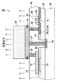
図1は、本発明のレイアウト方法を適用する半導体装置の一実施例のレイアウト概念図である。同図に示す半導体装置10は、不純物拡散領域が埋め込み酸化膜によりシリコン支持基板から絶縁分離された、すなわち、SOI(Silicon-On-Insulator)基板の活性層内に形成されたものである。そして、このような不純物拡散領域を有する2つのCMOS(相補型MOS)インバータ12,14が所定間隔離れた位置に配置され、第1金属配線16を介して直列に接続されている。
【0030】
ここで、それぞれのインバータ12,14は、P型およびN型MOSFET(電界効果トランジスタ)18および20を備えている。
【0031】
P型およびN型拡散領域(不純物拡散領域)22,24のソース領域は、それぞれ第1コンタクトホール(接続孔)26を介して電源配線およびグランド配線に接続されている。また、P型およびN型拡散領域22,24のドレイン領域は、第1コンタクトホール26を介して共に第1金属配線16に接続されている。また、P型およびN型拡散領域22,24の上を通過し、その左側のソース領域と右側のドレイン領域とを分けるようにゲート電極28が形成されている。
【0032】
図示例の半導体装置10において、第1金属配線16の総面積と第1金属配線16が接続されたP型およびN型拡散領域22,24(ドレイン領域)の面積との比は、第1金属配線16の加工(パターニング)、もしくは第1金属配線16を覆う第1層間絶縁膜(絶縁層)(図3参照)48の堆積のためのプラズマプロセスにおいて、P型およびN型MOSFET18および20の特性を劣化させない、所定の値以下に制限されている。
【0033】
ここで、第1金属配線16の総面積とは、プラズマプロセス中に、プラズマ雰囲気に晒される第1金属配線16の合計面積である。第1金属配線16の加工工程では第1金属配線16の側面積、第1層間絶縁膜の堆積工程では第1金属配線16の平面積と側面積の合計である。複数の第1金属層配線が同一の不純物拡散層にコンタクトホールを介して接続されている場合には、その複数の第1金属配線の面積の合計が、第1金属配線の総面積になる。また、P型およびN型拡散領域22,24の面積とは、SOI基板の活性層内に形成され、第1金属配線16にコンタクトホール26を介して接続された不純物拡散領域22,24の合計平面積である。
【0034】
本実施例では、第1金属配線16の総面積(側面積)とインバータ12,14のP型およびN型拡散領域22,24の面積との比(アンテナ比)を100:1に制限する。これにより、例えばインバータ12,14のドレイン領域22,24の合計面積が4μm2 である場合、第1金属配線16の総面積は400μm2 が上限となる。第1金属配線の厚さが0.4μmであるとすると、その配線長は400÷(0.4×2)=500μm以下に制限される。
【0035】
このように、第1金属配線16の総面積とその金属配線16に接続される不純物拡散領域の面積との比を所定の値以下に制限することにより、第1金属配線16および不純物拡散領域22,24に蓄積される電荷量を低く抑えることができるため、第1金属配線16の加工工程や、第1層間絶縁膜の堆積工程でのプラズマプロセスにおいて、P型およびN型MOSFET18および20の特性の劣化を防止することができる。
【0036】
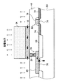
続いて、図2は、本発明のレイアウト方法を適用する半導体装置の別の実施例のレイアウト概念図である。同図に示す半導体装置30は、図1に示す半導体装置10において、さらに、2つのMOSインバータ12,14の間を接続する第1金属配線16に第1コンタクトホール26を介してダミーの不純物拡散領域32を不純物拡散領域22,24と並列に接続したものである。これにより、ダミー不純物拡散領域32は容量素子として用いられる。
【0037】
なお、前述の特開平8−97416号には、従来の半導体装置のゲート絶縁膜に対するプラズマダメージ対策として、金属配線とゲート電極との間にダイオードおよび抵抗を構成するN型拡散層を介在させることが提案されている。この従来技術のN型拡散層とは異なり、本願発明のダミー不純物拡散領域32は、埋め込み酸化膜によりシリコン支持基板から絶縁分離されているため、ダイオードとしては機能しない。また、この従来技術では、金属配線を切断し、N型拡散層を抵抗として直列に接続する。これに対して本発明では、金属配線を切断することなく、ダミー不純物拡散領域32を不純物拡散領域22,24と並列に接続する。
【0038】
ダミー不純物拡散領域32は、アンテナ比の制限を満足するように、第1金属配線16の総面積と不純物拡散領域22,24の面積との第1の比か、もしくは、第1金属配線16上に設けられるコンタクトホールの総面積と不純物拡散領域22,24の面積との第2の比が、これら第1および第2の比に対してそれぞれ定められた所定の値を超える場合に接続される。
【0039】
もしくは、これらの比が所定の値を超える可能性が高い箇所には、実際に超えているかいないかの検証を行うことなく、ダミー不純物拡散領域32を接続し、もしくはその他の方法による対策を行い、実際に所定の値を超えた場合であってもプラズマダメージによる劣化が起きないようにすることも可能である。例えば、半導体装置内の回路ブロックの出力端子と、同一半導体装置内の他の回路ブロックの入力端子とを接続する配線は、数mm以上の長さを有する場合が多い。このため、回路ブロックの出力端子を構成するMOSトランジスタの不純物拡散領域と、出力端子に接続される配線の面積との比は、所定の値を超える可能性が高い。
【0040】
図3の断面図に示すように、フォトレジスト34をマスクとする第1金属配線16の加工工程で、その側面から入射した荷電粒子は、不純物拡散領域25(22,24)/埋め込み酸化膜36/シリコン支持基板38により構成されるキャパシタに蓄積され、埋め込み酸化膜36の両端に電圧が印加される。プラズマプロセスで入射する電荷が一定量であるとすると、キャパシタの容量が大きいほど埋め込み酸化膜36に印加される電圧は低下し、その絶縁破壊を防止できる。
【0041】
従って、第1金属配線16に対して、不純物拡散領域25(すなわち、CMOSインバータ12のP型およびN型ドレイン拡散領域22,24)と並列にダミー不純物拡散領域32を付加することにより、合計のキャパシタが増加して、埋め込み酸化膜36に印加される電圧が低下する。すなわち、アンテナ比を本来の不純物拡散領域25とダミー不純物拡散領域32の合計で計算すればよく、アンテナ比を低減することが可能になる。
【0042】
なお、接続するダミー不純物拡散領域32の個数は1つに限定されず、必要に応じて、1本の第1金属配線16に複数個のダミー不純物拡散領域32を並列に接続してもよい。
【0043】
不純物拡散領域22,24の面積が大きい場合には、別の第1コンタクト孔26を介して別の第1金属配線16を不純物拡散領域22,24に接続し、その配線にダミー不純物拡散領域32を接続するようにしてもよい。
【0044】
ダミー不純物拡散領域32の代わりに、支持基板38に形成されるダイオードを接続してもよい。図4には、支持基板38と、その表面に形成された反対導電型の拡散領域との間に形成されたダイオード(P/N接合)を、第1金属配線16に接続した半導体装置40の断面図を示す。図では、P型の支持基板を利用する場合を例に、N型不純物拡散領域39を支持基板の表面に形成した例を示した。
【0045】
このようなN型不純物拡散領域39の形成のためには、例えば、MOSトランジスタ68,70のゲート電極28およびその側壁のサイドウォール29を形成した後に、N型不純物拡散領域39を形成すべき位置のフィールド酸化膜66および埋め込み酸化膜36をエッチングして開口を形成する。そして、NチャネルMOSトランジスタのソース、ドレイン領域を構成するN型拡散領域24の形成と同時に、この開口の底面の支持基板38の表面にN型不純物拡散領域39の形成を行う。その後、MOSトランジスタ68,70を覆うとともに、埋め込み酸化膜36に形成した開口を埋め込む層間絶縁膜48を堆積する。そしてこの層間絶縁膜48に、MOSトランジスタ68,70のソース、ドレイン領域やゲート電極に接続するための第1コンタクト孔26を形成すると同時に、N型不純物拡散層39に接続するための第1コンタクト孔26を形成し、第1金属配線16に接続する。
【0046】
この場合、シリコン支持基板38とN型不純物拡散領域39との間に形成されたP/N接合が、不純物拡散領域22,24とシリコン支持基板38との間のキャパシタに並列に接続される。そして、プラズマプロセスで入射し、蓄積された電荷によって不純物拡散領域22,24とシリコン支持基板38との間のキャパシタに印加される電圧が高くなると、P/N接合に電流が流れ、電荷が逃がされる。この結果、埋め込み酸化膜36に印加される電圧は低下し、その絶縁破壊を防止できる。
【0047】
第1金属配線16にダミー不純物拡散領域32やダイオードを接続する代わりに、図5の半導体装置50のように、第1金属配線16を途中で分割し、バッファ42を挿入してもよい。バッファ42は、2つのMOSインバータ44,46を直列に接続したものであり、論理は変化しない。このバッファ42を挿入することにより、第1金属配線16が2つに分割され、アンテナ比を低減することができる。
【0048】
なお、挿入するバッファ42の個数は1つに限定されず、必要に応じて、1本の第1金属配線16に複数個のバッファ42を直列に接続し、第1の金属配線16を複数に分割してもよい。
【0049】
前述のように、第1金属配線16にダミー不純物拡散領域32を接続すると、信号の伝搬経路に余分な容量が付加されるため、インバータ12からインバータ14への信号の伝搬遅延が増大する。これに対し、バッファ42を挿入する場合、この遅延の問題が生じないという利点がある。しかし、バッファ42を挿入する場合、第1金属配線16にダミー不純物拡散領域32を接続するよりも大きなレイアウト面積を必要とする。
【0050】
また、第1金属配線16にバッファ42を挿入して第1金属配線16を分割する代わりに、アンテナ比を満足するように第1金属配線16を分割し、分割後の配線を第1金属配線16よりも上層の配線を介して接続してもよい。この場合、第1金属配線16の加工工程時に上層の配線は存在せず、第1金属配線16は電気的に分断されているため、バッファ42を挿入した場合と同様の効果を得ることができる。
【0051】
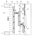
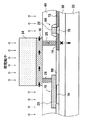
続いて、図6は、本発明のレイアウト方法を適用する半導体装置の別の実施例のレイアウト概念図である。同図に示す半導体装置60は、図1,2および5の場合と同じく、不純物拡散領域が埋め込み酸化膜によりシリコン支持基板から絶縁分離されたSOI基板(図3参照)を用いて形成されたものであり、CMOSインバータ52が、第1金属配線16および第2コンタクトホール54を介してパッド56に接続されている。
【0052】
ここで、パッド56は、信号を半導体装置60の外部に引き出すための電極であり、第1金属配線16が形成される第1金属配線層の上層に積層された第2金属配線層で形成されている。また、第2コンタクトホール54は、パッド56の外周部に沿って形成されている。半導体装置60上の全面にはパッシベーション膜があり、パッド56上部のパッシベーション膜が開孔され、パッド開口部58が形成されている。なお、インバータ52の構成は、図1に示すインバータ12,14と同じである。
【0053】
図示例の半導体装置60において、第1金属配線16上に設けられる第2コンタクトホール54の総面積(あるいは、第2コンタクトホール54の寸法が一定である場合には、その個数)とインバータ52のP型およびN型ドレイン拡散領域(不純物拡散領域)22,24の面積との比は、第2コンタクトホール54の形成のためのプラズマプロセスにおいて、P型およびN型MOSFET18および20の特性を劣化させない、所定の値以下に制限されている。
【0054】
ここで、ダメージを与える可能性のあるプラズマプロセスとしては、第2コンタクトホール54の開口のためのドライエッチングプロセスや、開口されたコンタクトホール54内に配線を形成する金属を堆積するためのスパッタプロセスがある。いずれの場合にも、アンテナルールの対象となる第2コンタクトホール54の総面積とは、プラズマプロセス中に、プラズマ雰囲気に晒される、第1金属配線16上に設けられた第2コンタクトホール54の穴底の合計面積である。
【0055】
また、パッド開口部58の面積とインバータ52のP型およびN型ドレイン拡散領域22,24の面積との比も、パッド開口部58を形成するためのプラズマプロセスにおいて、P型およびN型MOSFET18および20の特性を劣化させない、所定の値以下に制限されている。
【0056】
本実施例では、MOSインバータ52のP型およびN型ドレイン拡散領域22,24の面積と第2コンタクトホール56の個数との比を1μm2 当たり5個に制限し、P型およびN型ドレイン拡散領域22,24の面積とパッド開口部58の面積との比を1:100に制限する。これにより、例えば不純物拡散領域の面積が20μm2 の場合、第2コンタクトホールの個数は100個が上限となり、パッド開口部58の面積は2000μm2 が上限となる。
【0057】
このように、第1金属配線16上に設けられる第2コンタクトホール54の総面積や、パッド開口部58の面積とインバータ52のP型およびN型ドレイン拡散領域22,24の面積との比を所定の値以下に制限することにより、第2コンタクトホールやパッド開口部58の形成工程でのプラズマプロセスにおいて、P型およびN型MOSFET18および20の特性の劣化を防止することができる。
【0058】
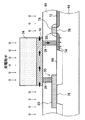
続いて、図7は、本発明のレイアウト方法を適用する半導体装置の別の実施例のレイアウト概念図である。同図に示す半導体装置70は、図6に示す半導体装置60において、さらに、パッド56の下層の同形の第1金属配線16の下に、第1コンタクトホール26を介してダミーの不純物拡散領域62を不純物拡散領域22,24と並列に接続したものである。これにより、ダミー不純物拡散領域62は容量素子として用いられる。
【0059】
ダミー不純物拡散領域62は、アンテナ比の制限を満足するように、第1金属配線16の総面積と不純物拡散領域22,24の面積との第1の比か、もしくは、第1金属配線16上に設けられる第2コンタクトホール54の総面積と不純物拡散領域22,24の面積との第2の比が、これら第1および第2の比に対してそれぞれ定められた所定の値を超える場合に接続される。なお、ダミー不純物拡散領域62の代わりに、図4に示されるようなダイオード(P/N接合)を接続してもよい。
【0060】
図2の場合と同様に、第1金属配線16に対して、P型およびN型拡散領域22,24と並列にダミー不純物拡散領域62を付加することにより、合計のキャパシタが増加されるので、アンテナ比を低減することが可能になる。
【0061】
なお、第1金属配線16の場合を例に挙げて説明したが、本発明はこれに限定されず、第1金属配線16よりも上層の金属配線の場合にも同様に適用可能である。下層に金属配線がある場合、プラズマ雰囲気に晒される上層の金属配線は、下層の金属配線や下層のコンタクトホールを介して電気的にMOSトランジスタの不純物拡散領域に接続される。また、同一の配線層の複数の金属配線が、下層の金属配線やコンタクトホールを通じて、同一の不純物拡散領域に接続される場合もある。その場合には、アンテナ比は、同一の配線層の複数の金属配線の総面積で評価する。配線の材料も限定されず、アルミ、タングステン等の各種の金属の他、シリサイド、ポリサイド等の従来公知の配線材料が全て利用可能である。
【0062】
また、アンテナ比の所定値は、SOI基板の仕様、例えば埋め込み酸化膜の膜厚や、プラズマプロセスで使用されている製造装置の種類、製造条件等に強く依存するため、実施例の値に限定されず、埋め込み酸化膜やMOSETに損傷を与えない範囲で、適宜最適な値に設定すればよい。
【0063】
実際の半導体装置のレイアウトを行う場合には、特開平11−186394号や特開平11−297836号に示されたように、回路ブロック(セル)の配置およびその間の配線を行った段階で、自動レイアウト装置の機能を利用して、アンテナ比の算出および、算出された比が所定の値を超える部分の抽出を自動的に行う。そして、抽出された部分に対して、適切な対策を、やはり自動レイアウト装置の機能を利用して、自動で、もしくは作業者が適切な対策を選択することによって、行う。
【0064】
アンテナ比の算出において対象となる配線の「総面積」は、前述のように、第1金属配線16の加工工程では第1金属配線の側面積であり、第1金属配線16上への第1層間絶縁膜堆積工程では、第1金属配線の平面積と側面積との合計である。従って、第1金属配線の側面積と、平面積と側面積の合計とのそれぞれについてアンテナ比を算出し、そのそれぞれに対して定めた所定の値との比較を行うことが好ましい。しかし、金属配線の加工工程と層間絶縁膜の堆積工程とのいずれか一方によるプラズマダメージの方が他方によるダメージに比較して大きい場合には、ダメージの大きい方に対応する総面積のみを求めてアンテナ比を算出し、所定の値との比較を行うようにしてもよい。もしくは、金属配線の平面積と側面積とのそれぞれについてアンテナ比を算出し、加工工程と層間絶縁膜堆積工程との両方におけるプラズマダメージを考慮してそれぞれに対して定めた所定の値との比較を行うようにしてもよい。
【0065】
また、それぞれの配線層の厚さは使用する製造プロセスによって決まっているため、配線の周辺長を求めることによって側面積を求めることができる。さらに、配線の長さのみを求めることによっても、側面積を近似的に求めることができる。平面積についても、現実に使用される配線の幅が実質的に一定とみなせる場合には、配線の長さを求めることによって近似的に求めることができる。従って、配線の総面積と不純物拡散領域の面積との比の算出、および算出した比の所定の値との比較は、近似的には、配線の長さと不純物拡散領域との面積比を求め、その比について定めた所定の値と比較することによって行うこともできる。
【0066】
アンテナ比の算出は、半導体装置の全体に対して行うことも可能であるし、所定の値を超える可能性が高いと予想される部分のみについて行うことも可能である。例えば、前述した回路ブロックの出力端子の場合、出力端子を構成する最終段のMOSトランジスタには、ほぼ同一の寸法のものが使用されることが多い。従って、不純物拡散領域の面積はほぼ一定であると考えられる。このような場合には、出力端子に接続される各配線層の配線の長さのみを調べることによって、アンテナ比を近似的に算出することも可能である。
【0067】
以上述べたように、本願発明における配線の総面積、もしくは接続孔の総面積と不純物拡散領域の面積との比の算出は、必ずしも厳密に行う必要はない。結果としてプラズマダメージによる劣化を防止できれば、さまざまな実用的な近似方法によって効率的に算出を行い、その算出方法に合わせた余裕を持って設定した所定の値との比較を行えばよい。
【0068】
本発明の半導体装置およびそのレイアウト方法は、基本的に以上のようなものである。
以上、本発明の半導体装置およびそのレイアウト方法について詳細に説明したが、本発明は上記実施例に限定されず、本発明の主旨を逸脱しない範囲において、種々の改良や変更をしてもよいのはもちろんである。
【0069】
図4には、支持基板38の表面に、支持基板と反対導電型の不純物拡散領域を形成し、第1金属配線16に接続して、プラズマダメージによる素子劣化防止のためのダイオードとして使用した例を示した。同様の製造工程で、支持基板と同一導電型の不純物拡散領域を支持基板表面に形成することも可能である。このような同一導電型の不純物拡散領域を、第1コンタクト孔26、第1金属配線16およびさらに上層の金属配線を介してパッドに接続し、さらに、そのパッドを介して、半導体装置を格納するパッケージの端子に接続することも可能である。そして、接続された端子をグランド端子とすることにより、もしくは、特定の電位を印加する端子とすることにより、支持基板の電位を固定することが可能になる。
【0070】
従来のSOI基板を利用した半導体装置においては、フリップチップBGA(Ball Grid Array )等の、支持基板の裏面がパッケージ端子に接続されない種類のパッケージに格納した場合、支持基板の電位を固定することができなかった。このため、支持基板電位の変動によって半導体装置の動作の不安定性が発生するという問題があった。
【0071】
支持基板の表面に支持基板と同一導電型の不純物拡散領域を形成し、パッドを介してパッケージの端子に接続することにより、従来のパッケージ技術をそのまま利用しながら、このような問題を解決することができる。
【0072】
【発明の効果】
以上詳細に説明した様に、本発明によれば、SOI基板上に形成された不純物拡散領域に接続される配線層の総面積、コンタクトホールの総面積やパッド開口部の面積を所定の値以下に制限することにより、プラズマプロセス中のチャージアップによる半導体素子の破壊を防止することができ、信頼性の高い半導体装置を実現すると共に、半導体装置の製造歩留りを向上させることができる。また、ダミー不純物拡散領域を付加したり、バッファを挿入することにより、また、下層の配線を分割し、かつ分割後の配線を上層の配線を介して接続することにより、アンテナ比を低減することが可能になり、回路設計上の制約を大幅に緩和することができる。
【図面の簡単な説明】
【図1】 本発明のレイアウト方法を適用する半導体装置の一実施例のレイアウト概念図である。
【図2】 本発明のレイアウト方法を適用する半導体装置の別の実施例のレイアウト概念図である。
【図3】 図2に示す半導体装置の一実施例の断面図である。
【図4】 本発明の半導体装置の別の実施例の断面図である。
【図5】 本発明のレイアウト方法を適用する半導体装置の別の実施例のレイアウト概念図である。
【図6】 本発明のレイアウト方法を適用する半導体装置の別の実施例のレイアウト概念図である。
【図7】 本発明のレイアウト方法を適用する半導体装置の別の実施例のレイアウト概念図である。
【図8】 ゲート酸化膜でプラズマダメージが発生する原理を表す一例の断面図である。
【図9】 ゲート酸化膜でプラズマダメージが発生する原理を表す別の例の断面図である。
【図10】 ゲート酸化膜でプラズマダメージが発生する原理を表す別の例の断面図である。
【図11】 ゲート酸化膜でプラズマダメージが発生しない場合の原理を表す一例の断面図である。
【図12】 SOI基板を用いる半導体装置において、埋め込み酸化膜でプラズマダメージが発生する原理を表す一例の断面図である。
【符号の説明】
10,30,40,50,60,70 半導体装置
12,14,44,46,52 インバータ
16,86 金属配線
18,20 MOSFET
22,24,25,72,74 不純物拡散領域
26,54,84 コンタクトホール
28,78 ゲート電極
29 サイドウォール
32,62 ダミー不純物拡散領域
36 埋め込み酸化膜
38 シリコン支持基板
39 N型不純物拡散領域
42 バッファ
48,80 層間絶縁膜
56 パッド
58 パッド開口部
64 シリコン基板
66 フィールド酸化膜
68,70 MOS型トランジスタ
76 ゲート絶縁膜
34,82,90 フォトレジスト
88 パッシベーション膜
92 パッド開口部[0001]
BACKGROUND OF THE INVENTION
The present invention relates to a semiconductor device using an SOI (Silicon-On-Insulator) substrate and a layout method thereof.
[0002]
[Prior art]
In the manufacturing process of a semiconductor device, various plasma processes such as plasma etching, sputtering, plasma CVD (chemical vapor deposition), and ion implantation are used.
[0003]
During this plasma process, when charged particles (ions, electrons) are incident on a semiconductor substrate on which metal wiring or other structures are formed on its surface, charges are applied to the floating metal wiring that is not connected to the semiconductor substrate. Accumulated and a charge-up phenomenon occurs. If the metal electrode is connected to the gate electrode of a MOS (Metal-Oxide Semiconductor) type semiconductor element (MOS type transistor), plasma damage may occur in the gate insulating film under the gate electrode. That is, when a high voltage is applied, the quality may deteriorate or dielectric breakdown may occur.
[0004]
Hereinafter, a specific example will be described.
[0005]
8 to 10 are cross-sectional views showing examples of the principle that plasma damage occurs in the gate oxide film. 8 is a plasma etching process of the first metal wiring, FIG. 9 is a plasma etching process of the second contact hole following FIG. 8, and FIG. 10 is a plasma etching process of the passivation film following FIG. FIG. 2 conceptually illustrates how a gate electrode of a MOS transistor is destroyed due to plasma damage.
[0006]
First, in FIG. 8, two
[0007]
In the
[0008]
A first interlayer
[0009]
In FIG. 8, a metal film for forming the
[0010]
In this case, the charged particles in the plasma atmosphere are incident from the side surface of the
[0011]
Subsequently, in FIG. 9, a second
[0012]
In this case, the charged particles are incident from the surface of the
[0013]
Subsequently, in FIG. 10, a
[0014]
In this case, charged particles are incident from the surface of the
[0015]
In this way, the metal wiring exposed to the plasma atmosphere acts as an antenna for capturing charged particles, and the metal wiring connected to the gate electrode directly or via the wiring of the lower wiring layer is flat during plasma etching. As the area (upper area), the side area, or the flat area of the contact hole or pad opening on the metal wiring increases, the gate insulating film deteriorates significantly. This phenomenon is generally called an antenna effect.
[0016]
In order to mitigate the plasma damage due to the antenna effect, a layout called an antenna rule is disclosed, for example, as disclosed in Japanese Patent Application Laid-Open Nos. 8-97416, 11-186394, 11-297836, and the like. In general, there are restrictions on design, and protective elements such as resistors and diodes are provided. For example, when a metal wiring not connected to the impurity diffusion region is connected to the gate electrode, conventionally, the ratio of the area of the metal wiring to the area of the gate electrode (antenna ratio) is limited to a predetermined value or less. ing.
[0017]
[Problems to be solved by the invention]
The conventional antenna rule is applied only when a metal wiring not connected to the semiconductor substrate is connected to the gate electrode. As shown in FIG. 11, if a part of the
[0018]
However, as shown in FIG. 12, in the semiconductor device using the SOI substrate, since the
[0019]
Further, as described above, when the impurity diffusion region is the source or drain of the MOS transistor, the MOS transistor is damaged even if it is a relatively slight charge-up that does not damage the buried oxide film. There are cases where problems such as an increase in leakage current between the source and the drain and a fluctuation in threshold voltage may occur.
[0020]
However, conventionally, there is a technique for preventing the breakdown of the gate insulating film, but no technique for preventing the dielectric breakdown of the buried
[0021]
An object of the present invention is to solve the problems based on the above-described conventional technology, and to prevent a semiconductor device using an SOI substrate without damage to a semiconductor element during a plasma process, and destruction of the semiconductor element due to charge-up during the plasma process. Another object of the present invention is to provide a layout method for a semiconductor device.
[0022]
[Means for Solving the Problems]
In order to achieve the above object, the present invention is insulated from a support substrate by a buried oxide film and reaches the buried oxide film.Film thicknessA MOS transistor having an impurity diffusion region formed in the first region as a drain region of an SOI substrate having an active layer separated into a plurality of regions including the first region by a field oxide film having a first region; In a semiconductor device having one wiring layer,
The first wiring layer has at least one wiring connected to the impurity diffusion region directly or via a wiring of a wiring layer lower than the first wiring layer;
The ratio of the total area of the at least one wiring to the area of the impurity diffusion region is such that the MOS in a plasma process for processing the first wiring layer or depositing an insulating layer covering the first wiring layer. It does not deteriorate the characteristics of the transistor, and is below a predetermined value.A semiconductor device is provided.
According to the present invention, an active layer is isolated from a support substrate by a buried oxide film and separated into a plurality of regions including a first region by a field oxide film having a thickness reaching the buried oxide film. In a semiconductor device comprising a SOI transistor having a MOS transistor having a drain region as an impurity diffusion region formed in the first region, and a first wiring layer,
The first wiring layer has at least one wiring connected to the impurity diffusion region directly or via a wiring of a wiring layer lower than the first wiring layer;
The ratio of the total area of the connection hole provided on the at least one wiring and the area of the impurity diffusion region is not more than a predetermined value that does not deteriorate the characteristics of the MOS transistor in the plasma process for forming the connection hole. A semiconductor device is provided.
Here, the MOS transistor preferably constitutes an inverter, and the drain region preferably constitutes an output terminal of the inverter.
[0023]
Further, the present invention is isolated from the support substrate by the buried oxide film and separated into a plurality of regions including the first and second regions by the field oxide film having a thickness reaching the buried oxide film. In a semiconductor device having an MOS substrate having a drain region of an impurity diffusion region formed in the first region of an SOI substrate having an active layer, and a first wiring layer,
The first wiring layer has at least one wiring connected to the impurity diffusion region directly or via a wiring of a wiring layer lower than the first wiring layer;
The dummy impurity diffusion region formed in the second region of the active layer is connected to the impurity diffusion region via the wiring of the first wiring layer or the wiring of the wiring layer below the first wiring layer. And
The ratio of the total area of the at least one wiring to the total area of the impurity diffusion region and the dummy impurity diffusion region is the processing of the first wiring layer or the insulating layer covering the first wiring layer There is provided a semiconductor device characterized in that the characteristics of the MOS transistor are not deteriorated in a plasma process for the deposition of the metal, and are not more than a predetermined value.
[0024]
Further, the present invention is isolated from the support substrate by the buried oxide film and separated into a plurality of regions including the first and second regions by the field oxide film having a thickness reaching the buried oxide film. In a semiconductor device having an MOS substrate having a drain region of an impurity diffusion region formed in the first region of an SOI substrate having an active layer, and a first wiring layer,
The first wiring layer has at least one wiring connected to the impurity diffusion region directly or via a wiring of a wiring layer lower than the first wiring layer;
The dummy impurity diffusion region formed in the second region of the active layer is connected to the impurity diffusion region via the wiring of the first wiring layer or the wiring of the wiring layer below the first wiring layer. And
The ratio of the total area of the connection hole provided on the at least one wiring and the total area of the impurity diffusion region and the dummy impurity diffusion region is determined by the plasma process for forming the connection hole. Provided is a semiconductor device characterized in that the characteristics are not more than a predetermined value without deteriorating characteristics.
[0025]
Further, the present invention is isolated from the support substrate by the buried oxide film and is separated into a plurality of regions including the first and second regions by the field oxide film having a thickness reaching the buried oxide film. An SOI substrate having an active layer, a MOS transistor having a drain region as an impurity diffusion region formed in the first region, and a first wiring layer,
A layout method of a semiconductor device having at least one wiring in which the first wiring layer is connected to the impurity diffusion region directly or via a wiring of a wiring layer below the first wiring layer Because
The ratio of the total area of the at least one wiring and the area of the impurity diffusion region is calculated, and the calculated ratio isThe characteristics of the MOS transistor are not deteriorated in a plasma process for processing the first wiring layer or depositing an insulating layer covering the first wiring layer.If it exceeds a predetermined value,
(1) The impurity diffusion region is formed in the second region of the active layer connected to the wiring of the first wiring layer or the wiring of the wiring layer below the first wiring layer. Insertion of dummy impurity diffusion regions,
(2) A P / N junction diode formed on the support substrate connected to the impurity diffusion region via a wiring of the first wiring layer or a wiring of a wiring layer below the first wiring layer. Insertion,
(3) Division of the at least one wiring and connection by wiring of a wiring layer above the first wiring layer;
(4) dividing the wiring of the wiring layer below the first wiring layer that connects the at least one wiring or the at least one wiring to the impurity diffusion region; andMOS inverter connected in seriesBufferTo the divisionInsert,
The present invention provides a layout method of a semiconductor device characterized in that any one of the above measures is taken.
[0026]
Further, the present invention is isolated from the support substrate by the buried oxide film and is separated into a plurality of regions including the first and second regions by the field oxide film having a thickness reaching the buried oxide film. An SOI substrate having an active layer, a MOS transistor having a drain region as an impurity diffusion region formed in the first region, and a first wiring layer,
A layout method of a semiconductor device having at least one wiring in which the first wiring layer is connected to the impurity diffusion region directly or via a wiring of a wiring layer below the first wiring layer Because
The ratio of the total area of the connection holes provided on the at least one wiring and the area of the impurity diffusion region is calculated, and the calculated ratio isThe characteristics of the MOS transistor are not deteriorated in a plasma process for processing the first wiring layer or depositing an insulating layer covering the first wiring layer.If it exceeds a predetermined value,
(1) The impurity diffusion region is formed in the second region of the active layer connected to the wiring of the first wiring layer or the wiring of the wiring layer below the first wiring layer. Insertion of dummy impurity diffusion regions,
(2) A P / N junction diode formed on the support substrate connected to the impurity diffusion region via a wiring of the first wiring layer or a wiring of a wiring layer below the first wiring layer. Insertion,
(3) Division of the at least one wiring and connection by wiring of a wiring layer above the first wiring layer;
(4) dividing the wiring of the wiring layer below the first wiring layer that connects the at least one wiring or the at least one wiring to the impurity diffusion region; andMOS inverter connected in seriesBufferTo the divisionInsert,
A layout method of a semiconductor device, characterized in that any one of the above measures is taken.
[0027]
Here, it is preferable that the countermeasure is insertion of the dummy impurity diffusion region.
Moreover, it is preferable that the said countermeasure is insertion of the said P / N junction diode.
Preferably, the MOS transistor constitutes an inverter, and the drain region constitutes an output terminal of the inverter.
[0028]
DETAILED DESCRIPTION OF THE INVENTION
Hereinafter, a semiconductor device and a layout method thereof according to the present invention will be described in detail based on preferred embodiments shown in the accompanying drawings.
[0029]
FIG. 1 is a layout conceptual diagram of an embodiment of a semiconductor device to which a layout method of the present invention is applied. The
[0030]
Here, each of the
[0031]
The source regions of the P-type and N-type diffusion regions (impurity diffusion regions) 22 and 24 are connected to the power supply wiring and the ground wiring through first contact holes (connection holes) 26, respectively. Further, the drain regions of the P-type and N-
[0032]
In the
[0033]
Here, the total area of the
[0034]
In this embodiment, the ratio (antenna ratio) between the total area (side area) of the
[0035]
Thus, by limiting the ratio of the total area of the
[0036]
Next, FIG. 2 is a layout conceptual diagram of another embodiment of a semiconductor device to which the layout method of the present invention is applied. The
[0037]
In addition, the above-mentionedJPNo. 8-97416 proposes interposing an N-type diffusion layer constituting a diode and a resistor between a metal wiring and a gate electrode as a countermeasure against plasma damage to a gate insulating film of a conventional semiconductor device. Unlike the conventional N-type diffusion layer, the dummy
[0038]
The dummy
[0039]
Alternatively, a dummy
[0040]
As shown in the cross-sectional view of FIG. 3, in the processing step of the
[0041]
Therefore, the dummy
[0042]
The number of dummy
[0043]
When the area of the
[0044]
Instead of the dummy
[0045]
In order to form such an N-type
[0046]
In this case, the P / N junction formed between the
[0047]
Instead of connecting the dummy
[0048]
The number of
[0049]
As described above, when the dummy
[0050]
Further, instead of inserting the
[0051]
Next, FIG. 6 is a layout conceptual diagram of another embodiment of a semiconductor device to which the layout method of the present invention is applied. The
[0052]
Here, the
[0053]
In the
[0054]
Here, examples of the plasma process that may cause damage include a dry etching process for opening the
[0055]
The ratio of the area of the
[0056]
In this embodiment, the ratio between the area of the P-type and N-type
[0057]
In this way, the ratio of the total area of the
[0058]
Next, FIG. 7 is a layout conceptual diagram of another embodiment of a semiconductor device to which the layout method of the present invention is applied. The
[0059]
The dummy
[0060]
As in the case of FIG. 2, by adding the dummy
[0061]
Although the case of the
[0062]
In addition, the predetermined value of the antenna ratio depends strongly on the specification of the SOI substrate, for example, the thickness of the buried oxide film, the type of manufacturing apparatus used in the plasma process, the manufacturing conditions, etc. However, the optimum value may be set as appropriate as long as the buried oxide film and the MOSET are not damaged.
[0063]
When an actual semiconductor device is laid out, as shown in Japanese Patent Application Laid-Open Nos. 11-186394 and 11-297836, the circuit blocks (cells) are arranged and wiring between them is performed automatically. Utilizing the function of the layout device, the antenna ratio is automatically calculated and the part where the calculated ratio exceeds a predetermined value is automatically extracted. Then, an appropriate countermeasure is taken for the extracted portion, either automatically using the function of the automatic layout apparatus, or by the operator selecting an appropriate countermeasure.
[0064]
As described above, the “total area” of the wirings that are subject to the calculation of the antenna ratio is the side area of the first metal wiring in the processing step of the
[0065]
Further, since the thickness of each wiring layer is determined by the manufacturing process to be used, the side area can be obtained by obtaining the peripheral length of the wiring. Furthermore, the side area can be approximately determined by determining only the length of the wiring. The plane area can also be approximately calculated by determining the length of the wiring when the width of the wiring actually used can be regarded as substantially constant. Therefore, the calculation of the ratio between the total area of the wiring and the area of the impurity diffusion region, and the comparison with the predetermined value of the calculated ratio, approximately, obtain the area ratio between the length of the wiring and the impurity diffusion region, It can also be done by comparing with a predetermined value defined for the ratio.
[0066]
The calculation of the antenna ratio can be performed on the entire semiconductor device, or can be performed only on a portion that is highly likely to exceed a predetermined value. For example, in the case of the output terminal of the circuit block described above, the MOS transistors at the final stage constituting the output terminal are often used with substantially the same dimensions. Therefore, the area of the impurity diffusion region is considered to be substantially constant. In such a case, it is also possible to approximately calculate the antenna ratio by examining only the wiring length of each wiring layer connected to the output terminal.
[0067]
As described above, the calculation of the total area of wiring or the ratio of the total area of connection holes and the area of the impurity diffusion region in the present invention is not necessarily strictly performed. As a result, if deterioration due to plasma damage can be prevented, the calculation can be efficiently performed by various practical approximation methods and compared with a predetermined value set with a margin according to the calculation method.
[0068]
The semiconductor device and its layout method of the present invention are basically as described above.
Although the semiconductor device and the layout method thereof according to the present invention have been described in detail above, the present invention is not limited to the above embodiments, and various improvements and modifications may be made without departing from the gist of the present invention. Of course.
[0069]
FIG. 4 shows an example in which an impurity diffusion region having a conductivity type opposite to that of the support substrate is formed on the surface of the
[0070]
In a conventional semiconductor device using an SOI substrate, the potential of the support substrate may be fixed when the back surface of the support substrate is stored in a package that is not connected to a package terminal, such as a flip chip BGA (Ball Grid Array). could not. For this reason, there has been a problem that the instability of the operation of the semiconductor device occurs due to the fluctuation of the support substrate potential.
[0071]
To solve such problems while using the conventional packaging technology as it is by forming an impurity diffusion region of the same conductivity type as the supporting substrate on the surface of the supporting substrate and connecting it to the terminal of the package through the pad. Can do.
[0072]
【The invention's effect】
As described above in detail, according to the present invention, the total area of the wiring layer connected to the impurity diffusion region formed on the SOI substrate, the total area of the contact hole, and the area of the pad opening are below a predetermined value. By limiting to the above, destruction of the semiconductor element due to charge-up during the plasma process can be prevented, a highly reliable semiconductor device can be realized, and the manufacturing yield of the semiconductor device can be improved. Also, the antenna ratio can be reduced by adding a dummy impurity diffusion region or inserting a buffer, or by dividing the lower layer wiring and connecting the divided wiring via the upper layer wiring. Therefore, restrictions on circuit design can be greatly eased.
[Brief description of the drawings]
FIG. 1 is a layout conceptual diagram of an embodiment of a semiconductor device to which a layout method of the present invention is applied.
FIG. 2 is a layout conceptual diagram of another embodiment of a semiconductor device to which the layout method of the present invention is applied.
3 is a cross-sectional view of one embodiment of the semiconductor device shown in FIG. 2;
FIG. 4 is a cross-sectional view of another embodiment of the semiconductor device of the present invention.
FIG. 5 is a layout conceptual diagram of another embodiment of a semiconductor device to which the layout method of the present invention is applied.
FIG. 6 is a layout conceptual diagram of another embodiment of a semiconductor device to which the layout method of the present invention is applied.
FIG. 7 is a layout conceptual diagram of another embodiment of a semiconductor device to which the layout method of the present invention is applied.
FIG. 8 is a cross-sectional view showing an example of the principle that plasma damage occurs in a gate oxide film.
FIG. 9 is a cross-sectional view of another example showing the principle that plasma damage occurs in a gate oxide film.
FIG. 10 is a cross-sectional view of another example showing the principle that plasma damage occurs in a gate oxide film.
FIG. 11 is a cross-sectional view showing an example of the principle when plasma damage does not occur in the gate oxide film.
FIG. 12 is a cross-sectional view showing an example of the principle that plasma damage occurs in a buried oxide film in a semiconductor device using an SOI substrate.
[Explanation of symbols]
10, 30, 40, 50, 60, 70 Semiconductor device
12, 14, 44, 46, 52 Inverter
16,86 metal wiring
18, 20 MOSFET
22, 24, 25, 72, 74 Impurity diffusion region
26, 54, 84 Contact hole
28, 78 Gate electrode
29 sidewall
32, 62 Dummy impurity diffusion region
36 buried oxide film
38 Silicon support substrate
39 N-type impurity diffusion region
42 buffers
48, 80 interlayer insulation film
56 pads
58 Pad opening
64 Silicon substrate
66 Field oxide film
68,70 MOS transistor
76 Gate insulation film
34, 82, 90 photoresist
88 Passivation film
92 Pad opening
Claims (10)
前記第1の配線層が、前記不純物拡散領域に、直接か、または、該第1の配線層より下層の配線層の配線を介して接続された、少なくとも1つの配線を有し、
前記少なくとも1つの配線の総面積と前記不純物拡散領域の面積との比が、前記第1の配線層の加工、もしくは該第1の配線層を覆う絶縁層の堆積のためのプラズマプロセスにおいて前記MOSトランジスタの特性を劣化させない、所定の値以下であることを特徴とする半導体装置。An SOI substrate having an active layer isolated from a support substrate by a buried oxide film and having an active layer separated into a plurality of regions including a first region by a field oxide film having a thickness reaching the buried oxide film. In a semiconductor device having a MOS transistor having a drain region as an impurity diffusion region formed in a first region, and a first wiring layer,
The first wiring layer has at least one wiring connected to the impurity diffusion region directly or via a wiring of a wiring layer lower than the first wiring layer;
The ratio of the total area of the at least one wiring to the area of the impurity diffusion region is such that the MOS in a plasma process for processing the first wiring layer or depositing an insulating layer covering the first wiring layer. A semiconductor device having a predetermined value or less that does not deteriorate characteristics of a transistor.
前記第1の配線層が、前記不純物拡散領域に、直接か、または、該第1の配線層より下層の配線層の配線を介して接続された、少なくとも1つの配線を有し、
前記少なくとも1つの配線上に設けられる接続孔の総面積と前記不純物拡散領域の面積との比が、該接続孔形成のためのプラズマプロセスにおいて前記MOSトランジスタの特性を劣化させない、所定の値以下であることを特徴とする半導体装置。An SOI substrate having an active layer isolated from a support substrate by a buried oxide film and having an active layer separated into a plurality of regions including a first region by a field oxide film having a thickness reaching the buried oxide film. In a semiconductor device having a MOS transistor having a drain region as an impurity diffusion region formed in a first region, and a first wiring layer,
The first wiring layer has at least one wiring connected to the impurity diffusion region directly or via a wiring of a wiring layer lower than the first wiring layer;
The ratio of the total area of the connection hole provided on the at least one wiring and the area of the impurity diffusion region is not more than a predetermined value that does not deteriorate the characteristics of the MOS transistor in the plasma process for forming the connection hole. There is a semiconductor device.
前記第1の配線層が、前記不純物拡散領域に、直接か、または、該第1の配線層より下層の配線層の配線を介して接続された、少なくとも1つの配線を有し、
前記活性層の第2の領域に形成されたダミー不純物拡散領域が、前記不純物拡散領域に、前記第1の配線層の配線もしくは前記第1の配線層より下層の配線層の配線を介して接続され、
前記少なくとも1つの配線の総面積と、前記不純物拡散領域と前記ダミー不純物拡散領域との合計の面積との比が、前記第1の配線層の加工、もしくは該第1の配線層を覆う絶縁層の堆積のためのプラズマプロセスにおいて前記MOSトランジスタの特性を劣化させない、所定の値以下であることを特徴とする半導体装置。An SOI substrate having an active layer isolated from a support substrate by a buried oxide film and separated into a plurality of regions including a first region and a second region by a field oxide film having a thickness reaching the buried oxide film A semiconductor device having a MOS transistor having a drain region as an impurity diffusion region formed in the first region, and a first wiring layer;
The first wiring layer has at least one wiring connected to the impurity diffusion region directly or via a wiring of a wiring layer lower than the first wiring layer;
The dummy impurity diffusion region formed in the second region of the active layer is connected to the impurity diffusion region via the wiring of the first wiring layer or the wiring of the wiring layer below the first wiring layer. And
The ratio of the total area of the at least one wiring to the total area of the impurity diffusion region and the dummy impurity diffusion region is the processing of the first wiring layer or the insulating layer covering the first wiring layer A semiconductor device having a predetermined value or less that does not deteriorate the characteristics of the MOS transistor in a plasma process for depositing silicon.
前記第1の配線層が、前記不純物拡散領域に、直接か、または、該第1の配線層より下層の配線層の配線を介して接続された、少なくとも1つの配線を有し、
前記活性層の第2の領域に形成されたダミー不純物拡散領域が、前記不純物拡散領域に、前記第1の配線層の配線もしくは前記第1の配線層より下層の配線層の配線を介して接続され、
前記少なくとも1つの配線上に設けられる接続孔の総面積と、前記不純物拡散領域と前記ダミー不純物拡散領域との合計の面積との比が、該接続孔形成のためのプラズマプロセスにおいて前記MOSトランジスタの特性を劣化させない、所定の値以下であることを特徴とする半導体装置。An SOI substrate having an active layer isolated from a support substrate by a buried oxide film and separated into a plurality of regions including a first region and a second region by a field oxide film having a thickness reaching the buried oxide film A semiconductor device having a MOS transistor having a drain region as an impurity diffusion region formed in the first region, and a first wiring layer;
The first wiring layer has at least one wiring connected to the impurity diffusion region directly or via a wiring of a wiring layer lower than the first wiring layer;
The dummy impurity diffusion region formed in the second region of the active layer is connected to the impurity diffusion region via the wiring of the first wiring layer or the wiring of the wiring layer below the first wiring layer. And
The ratio of the total area of the connection hole provided on the at least one wiring and the total area of the impurity diffusion region and the dummy impurity diffusion region is determined by the plasma process for forming the connection hole. A semiconductor device having a characteristic value not more than a predetermined value that does not deteriorate characteristics.
前記第1の配線層が、前記不純物拡散領域に、直接か、または、該第1の配線層より下層の配線層の配線を介して接続された、少なくとも1つの配線を有する半導体装置のレイアウト方法であって、
前記少なくとも1つの配線の総面積と前記不純物拡散領域の面積との比を算出し、該算出した比が、前記第1の配線層の加工、もしくは該第1の配線層を覆う絶縁層の堆積のためのプラズマプロセスにおいて前記MOSトランジスタの特性を劣化させない、所定の値を超える場合に、
(1)前記不純物拡散領域に、前記第1の配線層の配線もしくは前記第1の配線層より下層の配線層の配線を介して接続される、前記活性層の第2の領域に形成されたダミー不純物拡散領域の挿入、
(2)前記不純物拡散領域に、前記第1の配線層の配線もしくは前記第1の配線層より下層の配線層の配線を介して接続される、前記支持基板に形成されたP/N接合ダイオードの挿入、
(3)前記少なくとも1つの配線の分割、および、前記第1の配線層より上層の配線層の配線による接続、
(4)前記少なくとも1つの配線、もしくは、該少なくとも1つの配線を前記不純物拡散領域に接続する前記第1の配線層より下層の配線層の配線の、分割、および、MOSインバータを直列に接続したバッファの該分割箇所への挿入、
のいずれかの対策を行うことを特徴とする半導体装置のレイアウト方法。An SOI having an active layer isolated from a support substrate by a buried oxide film and separated into a plurality of regions including the first and second regions by a field oxide film having a thickness reaching the buried oxide film A MOS transistor having a drain region as an impurity diffusion region formed in the first region of the substrate, and a first wiring layer;
A layout method of a semiconductor device having at least one wiring in which the first wiring layer is connected to the impurity diffusion region directly or via a wiring of a wiring layer below the first wiring layer Because
A ratio between the total area of the at least one wiring and the area of the impurity diffusion region is calculated, and the calculated ratio is the processing of the first wiring layer or the deposition of the insulating layer covering the first wiring layer. In the case of exceeding a predetermined value that does not deteriorate the characteristics of the MOS transistor in the plasma process for
(1) The impurity diffusion region is formed in the second region of the active layer connected to the wiring of the first wiring layer or the wiring of the wiring layer below the first wiring layer. Insertion of dummy impurity diffusion regions,
(2) A P / N junction diode formed on the support substrate connected to the impurity diffusion region via a wiring of the first wiring layer or a wiring of a wiring layer below the first wiring layer. Insertion,
(3) Division of the at least one wiring and connection by wiring of a wiring layer above the first wiring layer;
(4) Dividing the at least one wiring or the wiring of the wiring layer below the first wiring layer connecting the at least one wiring to the impurity diffusion region, and connecting the MOS inverter in series Inserting the buffer into the segment ,
A layout method of a semiconductor device, characterized in that any one of the measures is taken.
前記第1の配線層が、前記不純物拡散領域に、直接か、または、該第1の配線層より下層の配線層の配線を介して接続された、少なくとも1つの配線を有する半導体装置のレイアウト方法であって、
前記少なくとも1つの配線上に設けられる接続孔の総面積と前記不純物拡散領域の面積との比を算出し、該算出した比が、前記第1の配線層の加工、もしくは該第1の配線層を覆う絶縁層の堆積のためのプラズマプロセスにおいて前記MOSトランジスタの特性を劣化させない、所定の値を超える場合に、
(1)前記不純物拡散領域に、前記第1の配線層の配線もしくは前記第1の配線層より下層の配線層の配線を介して接続される、前記活性層の第2の領域に形成されたダミー不純物拡散領域の挿入、
(2)前記不純物拡散領域に、前記第1の配線層の配線もしくは前記第1の配線層より下層の配線層の配線を介して接続される、前記支持基板に形成されたP/N接合ダイオードの挿入、
(3)前記少なくとも1つの配線の分割、および、前記第1の配線層より上層の配線層の配線による接続、
(4)前記少なくとも1つの配線、もしくは、該少なくとも1つの配線を前記不純物拡散領域に接続する前記第1の配線層より下層の配線層の配線の、分割、および、MOSインバータを直列に接続したバッファの該分割箇所への挿入、
のいずれかの対策を行うことを特徴とする半導体装置のレイアウト方法。An SOI having an active layer isolated from a support substrate by a buried oxide film and separated into a plurality of regions including the first and second regions by a field oxide film having a thickness reaching the buried oxide film A MOS transistor having a drain region as an impurity diffusion region formed in the first region of the substrate, and a first wiring layer;
A layout method of a semiconductor device having at least one wiring in which the first wiring layer is connected to the impurity diffusion region directly or via a wiring of a wiring layer below the first wiring layer Because
The ratio of the total area of the connection holes provided on the at least one wiring and the area of the impurity diffusion region is calculated, and the calculated ratio is the processing of the first wiring layer or the first wiring layer. When the plasma process for depositing the insulating layer covering the above does not deteriorate the characteristics of the MOS transistor and exceeds a predetermined value,
(1) The impurity diffusion region is formed in the second region of the active layer connected to the wiring of the first wiring layer or the wiring of the wiring layer below the first wiring layer. Insertion of dummy impurity diffusion regions,
(2) A P / N junction diode formed on the support substrate connected to the impurity diffusion region via a wiring of the first wiring layer or a wiring of a wiring layer below the first wiring layer. Insertion,
(3) Division of the at least one wiring and connection by wiring of a wiring layer above the first wiring layer;
(4) Dividing the at least one wiring or the wiring of the wiring layer below the first wiring layer connecting the at least one wiring to the impurity diffusion region, and connecting the MOS inverter in series Inserting the buffer into the segment ,
A layout method of a semiconductor device, characterized in that any one of the measures is taken.
Priority Applications (4)
| Application Number | Priority Date | Filing Date | Title |
|---|---|---|---|
| JP2001330276A JP4176342B2 (en) | 2001-10-29 | 2001-10-29 | Semiconductor device and layout method thereof |
| US10/280,022 US6815771B2 (en) | 2001-10-29 | 2002-10-25 | Silicon on insulator device and layout method of the same |
| US10/956,049 US20050059202A1 (en) | 2001-10-29 | 2004-10-04 | Silicon on insulator device and layout method of the same |
| US10/956,094 US7160786B2 (en) | 2001-10-29 | 2004-10-04 | Silicon on insulator device and layout method of the same |
Applications Claiming Priority (1)
| Application Number | Priority Date | Filing Date | Title |
|---|---|---|---|
| JP2001330276A JP4176342B2 (en) | 2001-10-29 | 2001-10-29 | Semiconductor device and layout method thereof |
Related Child Applications (1)
| Application Number | Title | Priority Date | Filing Date |
|---|---|---|---|
| JP2008189806A Division JP2008294463A (en) | 2008-07-23 | 2008-07-23 | Semiconductor device |
Publications (3)
| Publication Number | Publication Date |
|---|---|
| JP2003133559A JP2003133559A (en) | 2003-05-09 |
| JP2003133559A5 JP2003133559A5 (en) | 2005-06-30 |
| JP4176342B2 true JP4176342B2 (en) | 2008-11-05 |
Family
ID=19146023
Family Applications (1)
| Application Number | Title | Priority Date | Filing Date |
|---|---|---|---|
| JP2001330276A Expired - Fee Related JP4176342B2 (en) | 2001-10-29 | 2001-10-29 | Semiconductor device and layout method thereof |
Country Status (2)
| Country | Link |
|---|---|
| US (3) | US6815771B2 (en) |
| JP (1) | JP4176342B2 (en) |
Families Citing this family (36)
| Publication number | Priority date | Publication date | Assignee | Title |
|---|---|---|---|---|
| KR100487950B1 (en) * | 2003-02-03 | 2005-05-06 | 삼성전자주식회사 | Semiconductor device having a contact hole disposed on a gate electrode overlapped with an active region |
| JP2005116623A (en) * | 2003-10-03 | 2005-04-28 | Nec Electronics Corp | Semiconductor device and manufacturing method thereof |
| US20050242439A1 (en) * | 2004-04-28 | 2005-11-03 | International Business Machines Corporation | Method and structure for connecting ground/power networks to prevent charge damage in silicon on insulator |
| US7439152B2 (en) * | 2004-08-27 | 2008-10-21 | Micron Technology, Inc. | Methods of forming a plurality of capacitors |
| JP4726462B2 (en) * | 2004-10-29 | 2011-07-20 | ルネサスエレクトロニクス株式会社 | Semiconductor integrated device, design method thereof, design device, program, manufacturing method, and manufacturing device |
| US7651897B2 (en) * | 2004-12-07 | 2010-01-26 | National Semiconductor Corporation | Integrated circuit with metal heat flow path coupled to transistor and method for manufacturing such circuit |
| JP4507091B2 (en) * | 2004-12-13 | 2010-07-21 | エルピーダメモリ株式会社 | Semiconductor device manufacturing method and semiconductor device |
| CN101950748B (en) * | 2005-01-28 | 2013-06-12 | 株式会社半导体能源研究所 | Semiconductor device and method for manufacturing the same |
| US8112326B2 (en) * | 2005-02-03 | 2012-02-07 | TimeSight Systems, Inc. | Inventory management tracking control system |
| JP2006294719A (en) * | 2005-04-07 | 2006-10-26 | Oki Electric Ind Co Ltd | Semiconductor apparatus |
| US7688272B2 (en) * | 2005-05-30 | 2010-03-30 | Semiconductor Energy Laboratory Co., Ltd. | Semiconductor device |
| JP2007103809A (en) * | 2005-10-07 | 2007-04-19 | Oki Electric Ind Co Ltd | Semiconductor device and manufacturing method thereof |
| US7612399B2 (en) * | 2005-11-08 | 2009-11-03 | Samsung Electronics Co., Ltd. | Semiconductor integrated circuit devices |
| JP4947964B2 (en) * | 2005-12-05 | 2012-06-06 | ラピスセミコンダクタ株式会社 | Semiconductor device and manufacturing method thereof |
| JP2007299898A (en) * | 2006-04-28 | 2007-11-15 | Matsushita Electric Ind Co Ltd | Semiconductor device and layout design method of semiconductor device |
| US20070271540A1 (en) * | 2006-05-16 | 2007-11-22 | International Business Machines Corporation | Structure and method for reducing susceptibility to charging damage in soi designs |
| JP4996166B2 (en) * | 2006-08-09 | 2012-08-08 | ラピスセミコンダクタ株式会社 | Semiconductor device and manufacturing method of semiconductor device |
| US7880267B2 (en) | 2006-08-28 | 2011-02-01 | Micron Technology, Inc. | Buried decoupling capacitors, devices and systems including same, and methods of fabrication |
| KR100817094B1 (en) | 2007-03-27 | 2008-03-26 | 삼성전자주식회사 | Layout method of semiconductor device with protection junction diode from damage due to plasma charging |
| JP2008251812A (en) | 2007-03-30 | 2008-10-16 | Toshiba Corp | Semiconductor device, and manufacturing method thereof |
| JP2010016164A (en) * | 2008-07-03 | 2010-01-21 | Nec Electronics Corp | Method for designing semiconductor integrated circuit, manufacturing method, circuit design program, and semiconductor integrated circuit |
| JP2011175455A (en) * | 2010-02-24 | 2011-09-08 | Renesas Electronics Corp | Semiconductor integrated circuit device, design method, design device and program |
| TWI605549B (en) * | 2010-08-06 | 2017-11-11 | 半導體能源研究所股份有限公司 | Semiconductor device |
| JP5766462B2 (en) * | 2011-02-24 | 2015-08-19 | ローム株式会社 | Semiconductor device and manufacturing method thereof |
| JP6355460B2 (en) | 2014-07-08 | 2018-07-11 | ルネサスエレクトロニクス株式会社 | Semiconductor device and manufacturing method thereof |
| WO2016079918A1 (en) * | 2014-11-19 | 2016-05-26 | 株式会社ソシオネクスト | Layout structure of semiconductor integrated circuit |
| CN106876873A (en) * | 2016-12-20 | 2017-06-20 | 西安科锐盛创新科技有限公司 | The preparation method of the GaAs base plasma pin diodes of frequency reconfigurable dipole antenna |
| CN106898857A (en) * | 2016-12-20 | 2017-06-27 | 西安科锐盛创新科技有限公司 | The preparation method of Ge fundamental frequency restructural sleeve-dipole antennas |
| CN106785332A (en) * | 2016-12-20 | 2017-05-31 | 西安科锐盛创新科技有限公司 | It is applied to the preparation method of the heterogeneous SPiN diodes of Ge bases of restructural loop aerial |
| CN106847680B (en) * | 2016-12-20 | 2021-03-05 | 西安科锐盛创新科技有限公司 | Preparation method of GaAs-based frequency reconfigurable sleeve dipole antenna |
| CN106816685A (en) * | 2016-12-20 | 2017-06-09 | 西安科锐盛创新科技有限公司 | The manufacturing process of the SPIN diode components of frequency reconfigurable dipole antenna |
| CN106876872A (en) * | 2016-12-20 | 2017-06-20 | 西安科锐盛创新科技有限公司 | The preparation method of the Ge base restructural dipole antennas based on AlAs/Ge/AlAs structures |
| CN106785333A (en) * | 2016-12-20 | 2017-05-31 | 西安科锐盛创新科技有限公司 | For the pin diode preparation methods of the GaAs Ge GaAs heterojunction structures of multilayer holographic antenna |
| CN106785335A (en) * | 2016-12-20 | 2017-05-31 | 西安科锐盛创新科技有限公司 | The preparation technology of the Ge base plasma pin diodes of frequency reconfigurable dipole antenna |
| JP7071252B2 (en) * | 2018-09-28 | 2022-05-18 | ルネサスエレクトロニクス株式会社 | Semiconductor devices and their manufacturing methods |
| KR102496371B1 (en) | 2018-10-30 | 2023-02-07 | 삼성전자주식회사 | Semiconductor device |
Family Cites Families (35)
| Publication number | Priority date | Publication date | Assignee | Title |
|---|---|---|---|---|
| US4149176A (en) * | 1975-07-18 | 1979-04-10 | Tokyo Shibaura Electric Co., Ltd. | Complementary MOSFET device |
| JP2812388B2 (en) | 1988-01-18 | 1998-10-22 | 富士通株式会社 | Method of manufacturing SOI semiconductor device |
| US4965872A (en) * | 1988-09-26 | 1990-10-23 | Vasudev Prahalad K | MOS-enhanced, self-aligned lateral bipolar transistor made of a semiconductor on an insulator |
| JP3108447B2 (en) | 1991-03-08 | 2000-11-13 | 富士通株式会社 | Semiconductor device and manufacturing method thereof |
| JPH06204467A (en) | 1992-12-28 | 1994-07-22 | Matsushita Electric Ind Co Ltd | Semiconductor integrated circuit device and its manufacture |
| DE69417944T2 (en) | 1993-04-30 | 1999-12-09 | Ibm | Process for producing a protective diode against electrostatic discharge in silicon-on-insulator technology |
| JPH07106579A (en) | 1993-10-08 | 1995-04-21 | Hitachi Ltd | Semiconductor device and its manufacture |
| JP3450909B2 (en) | 1994-09-27 | 2003-09-29 | 三菱電機株式会社 | Semiconductor device |
| WO1996015553A1 (en) | 1994-11-15 | 1996-05-23 | Advanced Micro Devices, Inc. | Transistor structure with specific gate and pad areas |
| US5852317A (en) | 1995-03-31 | 1998-12-22 | National Semiconductor Corporation | Method to reduce gate oxide damage due to non-uniform plasmas in read only memory arrays |
| JP3527034B2 (en) * | 1996-09-20 | 2004-05-17 | 株式会社半導体エネルギー研究所 | Semiconductor device |
| JP3105815B2 (en) * | 1997-03-28 | 2000-11-06 | 日本電気株式会社 | Semiconductor integrated circuit device |
| US6432726B2 (en) | 1997-03-31 | 2002-08-13 | Artisan Components, Inc. | Method and apparatus for reducing process-induced charge buildup |
| JP3331304B2 (en) | 1997-05-27 | 2002-10-07 | シャープ株式会社 | Method for manufacturing semiconductor device |
| JP3111947B2 (en) * | 1997-10-28 | 2000-11-27 | 日本電気株式会社 | Semiconductor device and manufacturing method thereof |
| US6392277B1 (en) * | 1997-11-21 | 2002-05-21 | Hitachi, Ltd. | Semiconductor device |
| JP4063936B2 (en) | 1997-12-19 | 2008-03-19 | 松下電器産業株式会社 | Manufacturing method of semiconductor integrated circuit |
| DE69839780D1 (en) * | 1997-12-19 | 2008-09-04 | Advanced Micro Devices Inc | SILICON ON AN ISOLATOR CONFIGURATION WHICH IS COMPATIBLE WITH THE MASS CMOS ARCHITECTURE |
| JPH11204767A (en) | 1998-01-16 | 1999-07-30 | Mitsubishi Electric Corp | Semiconductor device |
| JP3461443B2 (en) | 1998-04-07 | 2003-10-27 | 松下電器産業株式会社 | Semiconductor device, semiconductor device design method, recording medium, and semiconductor device design support device |
| US6191020B1 (en) | 1998-05-21 | 2001-02-20 | Taiwan Semiconductor Manufacturing Company, Ltd. | Conductive interconnection for semiconductor integrated circuit and method of forming the same |
| JP3414656B2 (en) * | 1998-11-16 | 2003-06-09 | シャープ株式会社 | Semiconductor device and manufacturing method thereof |
| US6292927B1 (en) | 1998-12-07 | 2001-09-18 | Artisan Components, Inc. | Reduction of process antenna effects in integrated circuits |
| JP3298528B2 (en) | 1998-12-10 | 2002-07-02 | 日本電気株式会社 | Circuit design method and device, information storage medium, integrated circuit device |
| US6188122B1 (en) * | 1999-01-14 | 2001-02-13 | International Business Machines Corporation | Buried capacitor for silicon-on-insulator structure |
| US6150261A (en) | 1999-05-25 | 2000-11-21 | United Microelectronics Corp. | Method of fabricating semiconductor device for preventing antenna effect |
| US6358791B1 (en) * | 1999-06-04 | 2002-03-19 | International Business Machines Corporation | Method for increasing a very-large-scale-integrated (VLSI) capacitor size on bulk silicon and silicon-on-insulator (SOI) wafers and structure formed thereby |
| JP3885860B2 (en) * | 2000-01-14 | 2007-02-28 | セイコーエプソン株式会社 | Semiconductor memory device and manufacturing method thereof |
| US6475838B1 (en) * | 2000-03-14 | 2002-11-05 | International Business Machines Corporation | Methods for forming decoupling capacitors |
| JP4776752B2 (en) * | 2000-04-19 | 2011-09-21 | ルネサスエレクトロニクス株式会社 | Semiconductor device |
| JP2002026311A (en) * | 2000-07-04 | 2002-01-25 | Miyazaki Oki Electric Co Ltd | Soi type mos element and manufacturing method thereof |
| US6303414B1 (en) | 2000-07-12 | 2001-10-16 | Chartered Semiconductor Manufacturing Ltd. | Method of forming PID protection diode for SOI wafer |
| US6498372B2 (en) * | 2001-02-16 | 2002-12-24 | International Business Machines Corporation | Conductive coupling of electrical structures to a semiconductor device located under a buried oxide layer |
| US6979868B2 (en) * | 2001-04-18 | 2005-12-27 | United Microelectronics Corp. | Bypass circuits for reducing plasma damage |
| JP2003100899A (en) * | 2001-09-27 | 2003-04-04 | Mitsubishi Electric Corp | Semiconductor device and its manufacturing method |
-
2001
- 2001-10-29 JP JP2001330276A patent/JP4176342B2/en not_active Expired - Fee Related
-
2002
- 2002-10-25 US US10/280,022 patent/US6815771B2/en not_active Expired - Lifetime
-
2004
- 2004-10-04 US US10/956,094 patent/US7160786B2/en not_active Expired - Lifetime
- 2004-10-04 US US10/956,049 patent/US20050059202A1/en not_active Abandoned
Also Published As
| Publication number | Publication date |
|---|---|
| US20050059202A1 (en) | 2005-03-17 |
| JP2003133559A (en) | 2003-05-09 |
| US6815771B2 (en) | 2004-11-09 |
| US7160786B2 (en) | 2007-01-09 |
| US20030080385A1 (en) | 2003-05-01 |
| US20050042806A1 (en) | 2005-02-24 |
Similar Documents
| Publication | Publication Date | Title |
|---|---|---|
| JP4176342B2 (en) | Semiconductor device and layout method thereof | |
| US6611024B2 (en) | Method of forming PID protection diode for SOI wafer | |
| US7355252B2 (en) | Electrostatic discharge protection device and method of fabricating the same | |
| US7879650B2 (en) | Method of providing protection against charging damage in hybrid orientation transistors | |
| US20010042887A1 (en) | Integrated circuit devices that use antiparallel diodes to reduce damage during plasma processing | |
| US6611027B2 (en) | Protection transistor with improved edge structure | |
| US6462384B2 (en) | Semiconductor device for ESD protection | |
| US5932917A (en) | Input protective circuit having a diffusion resistance layer | |
| US20070205465A1 (en) | Semiconductor device and fabrication method thereof | |
| JP3897339B2 (en) | Structure and method for minimizing plasma charging damage of SOI devices | |
| US8026552B2 (en) | Protection element and fabrication method for the same | |
| US5736772A (en) | Bifurcated polysilicon gate electrodes and fabrication methods | |
| JP4205732B2 (en) | Semiconductor integrated circuit device | |
| US6768201B1 (en) | Semiconductor device and method for fabricating the same | |
| JP3574359B2 (en) | Semiconductor device | |
| US6573576B2 (en) | Semiconductor device and method for fabricating the same | |
| JP2008294463A (en) | Semiconductor device | |
| JP4601919B2 (en) | Manufacturing method of semiconductor device | |
| JP3254549B2 (en) | Semiconductor device and manufacturing method thereof | |
| JPH0324056B2 (en) | ||
| JP2730532B2 (en) | Semiconductor device | |
| JP3206652B2 (en) | Semiconductor device and method of manufacturing semiconductor device | |
| JP3132480B2 (en) | Method for manufacturing semiconductor device | |
| JPS61120459A (en) | Manufacture of semiconductor integrated circuit | |
| KR100575861B1 (en) | structure of ESD protection in semiconductor device |
Legal Events
| Date | Code | Title | Description |
|---|---|---|---|
| A521 | Request for written amendment filed |
Free format text: JAPANESE INTERMEDIATE CODE: A523 Effective date: 20041025 |
|
| A621 | Written request for application examination |
Free format text: JAPANESE INTERMEDIATE CODE: A621 Effective date: 20041025 |
|
| A977 | Report on retrieval |
Free format text: JAPANESE INTERMEDIATE CODE: A971007 Effective date: 20060126 |
|
| A131 | Notification of reasons for refusal |
Free format text: JAPANESE INTERMEDIATE CODE: A131 Effective date: 20080527 |
|
| A521 | Request for written amendment filed |
Free format text: JAPANESE INTERMEDIATE CODE: A523 Effective date: 20080723 |
|
| TRDD | Decision of grant or rejection written | ||
| A01 | Written decision to grant a patent or to grant a registration (utility model) |
Free format text: JAPANESE INTERMEDIATE CODE: A01 Effective date: 20080812 |
|
| A01 | Written decision to grant a patent or to grant a registration (utility model) |
Free format text: JAPANESE INTERMEDIATE CODE: A01 |
|
| A61 | First payment of annual fees (during grant procedure) |
Free format text: JAPANESE INTERMEDIATE CODE: A61 Effective date: 20080820 |
|
| FPAY | Renewal fee payment (event date is renewal date of database) |
Free format text: PAYMENT UNTIL: 20110829 Year of fee payment: 3 |
|
| R150 | Certificate of patent or registration of utility model |
Free format text: JAPANESE INTERMEDIATE CODE: R150 Ref document number: 4176342 Country of ref document: JP Free format text: JAPANESE INTERMEDIATE CODE: R150 |
|
| FPAY | Renewal fee payment (event date is renewal date of database) |
Free format text: PAYMENT UNTIL: 20110829 Year of fee payment: 3 |
|
| FPAY | Renewal fee payment (event date is renewal date of database) |
Free format text: PAYMENT UNTIL: 20120829 Year of fee payment: 4 |
|
| FPAY | Renewal fee payment (event date is renewal date of database) |
Free format text: PAYMENT UNTIL: 20120829 Year of fee payment: 4 |
|
| FPAY | Renewal fee payment (event date is renewal date of database) |
Free format text: PAYMENT UNTIL: 20130829 Year of fee payment: 5 |
|
| R250 | Receipt of annual fees |
Free format text: JAPANESE INTERMEDIATE CODE: R250 |
|
| R250 | Receipt of annual fees |
Free format text: JAPANESE INTERMEDIATE CODE: R250 |
|
| S111 | Request for change of ownership or part of ownership |
Free format text: JAPANESE INTERMEDIATE CODE: R313111 Free format text: JAPANESE INTERMEDIATE CODE: R313113 |
|
| R350 | Written notification of registration of transfer |
Free format text: JAPANESE INTERMEDIATE CODE: R350 |
|
| S531 | Written request for registration of change of domicile |
Free format text: JAPANESE INTERMEDIATE CODE: R313531 |
|
| R350 | Written notification of registration of transfer |
Free format text: JAPANESE INTERMEDIATE CODE: R350 |
|
| LAPS | Cancellation because of no payment of annual fees |