JP3879363B2 - ID card manufacturing method - Google Patents
ID card manufacturing method Download PDFInfo
- Publication number
- JP3879363B2 JP3879363B2 JP2000120046A JP2000120046A JP3879363B2 JP 3879363 B2 JP3879363 B2 JP 3879363B2 JP 2000120046 A JP2000120046 A JP 2000120046A JP 2000120046 A JP2000120046 A JP 2000120046A JP 3879363 B2 JP3879363 B2 JP 3879363B2
- Authority
- JP
- Japan
- Prior art keywords
- card
- curable protective
- card substrate
- protective member
- thermal transfer
- Prior art date
- Legal status (The legal status is an assumption and is not a legal conclusion. Google has not performed a legal analysis and makes no representation as to the accuracy of the status listed.)
- Expired - Fee Related
Links
Images


Landscapes
- Credit Cards Or The Like (AREA)
Description
【0001】
【発明の属する技術分野】
この発明は偽変造防止等が要求される画像保護層付きの顔画像入りカードに適用して好適なIDカードの製造方法に関するものである。
【0002】
【従来の技術】
近年、官公庁、銀行、会社、医療機関及び学校などのサービス産業分野では、身分証明書、パスポート、外国人登録証、図書館利用カード、キャッシュカード、クレジットカード、自動車免許証等の免許証類、従業者証、社員証、会員証、医療カード及び学生証などのIDカードが普及されている。この種のIDカードには、本人確認用の顔画像、及び所有者に関する文字や記号などの文字情報画像が記録されている。このため、IDカードの偽変造防止を目的とする印刷等が施される場合が多い。
【0003】
この顔画像は通常の場合、多階調を有するフルカラー画像によって、例えば、昇華型感熱転写記録方式、ハロゲン化銀カラー写真方式等により形成される。また、文字情報画像は二値画像より成り、例えば、溶融型感熱転写記録方式、昇華型感熱転写記録方式、ハロゲン化銀カラー写真方式、電子写真方式、インクジェット方式等により形成されている。更に、偽変造防止の目的ではホログラム、細紋等が採用されている。その他にIDカードには予め定型フォーマット印刷が必要に応じて施される。
【0004】
これらの画像を保護するために、IDカードの表面には必要に応じて保護層が設けられる。IDカードに設けられる保護層としては、例えば、特開平6−222535号、同6−222536号、同6−222537号に記載のように、カード表面に紫外線硬化性樹脂を塗布した後に、紫外線を照射し硬化せしめて保護層を設ける方法、また、特開平2−139551号に記載のようにラミネート保護層を設ける方法、ハロゲン化銀による写真表面にイソシアネート化合物を塗布した後に加熱硬化して保護層を設ける方法、及び、同8−224982号に記載のように、硬化性転写箔部材を転写して転写保護層を設ける方法が開示されている。
【0005】
【発明が解決しようとする課題】
ところで、硬化型転写箔部材を使用した従来方式のIDカードの製造方法によれば、この種の転写箔部材が紫外線によって硬化する性質を有していることから、硬化型転写箔部材が厚いほどカード基板上の表面保護性が良くなる。その反面、あまり膜厚が厚いと転写箔部材形成時における加工性が悪くなることを見出した。例えば、IDカードの端部にいわゆる目視可能なバリが発生する。以後、カード基板の外周縁を越えて外側にはみ出した保護層を外バリといい、また、カード基板の外周縁近隣で保護層がきちんと形成されていない場合に、内バリが発生しているという。
【0006】
この種のバリが発生すると次のような問題が発生する。外バリが発生した場合には、上述のはみ出し保護層、つまり、部材残留片の除去に手間を要したり、また、内バリ、外バリが発生した場合、共に、保護層の剥がれの原因となったりすることがあることを見出した。
【0007】
また、硬化型転写箔部材を薄くすれば、転写箔部材形成時におけるバリの発生を抑制できるが表面保護性は低下してしまうことを見出した。例えば、カード完成後の記録画像上を強く擦すると、硬化型転写箔部材(以下硬化型保護部材ともいう)上に傷を生じ、その傷が記録画像上に残ってしまうという問題があることを見出したのである。
【0008】
そこで、この発明は上述した課題を解決したものであって、顔画像や文字記録画像が形成されたカード基板に硬化型保護部材を設けて保護する場合に、その保護部材形成時における加工性を悪化させることなく、しかも、カード基板上の表面保護性を確保できるようにしたIDカードの製造方法を提供することを目的とする。
【0010】
【課題を解決するための手段】
上記問題点を解決するために、本発明者らは、カード基板上の表面保護性及び保護部材形成時の加工性に関して最適な硬化型保護部材の膜厚値を見い出すべく実験をした。この実験結果によれば、記録画像形成面側のカード基板上に透明性の硬化型保護部材を覆って保護する場合に、その硬化型保護部材の膜厚を0.5μm乃至5.0μmに規定し、その接着力Fbを、
0.5g/ cm <Fb<25g/ cm
に規定したときに、その保護部材形成時における加工性を悪化させることなく、しかも、カード基板上の表面保護性に優れ、かつ、耐擦過性(耐摩耗性)に優れたIDカードを提供できることが明らかになった。
【0011】
本発明のIDカードの製造方法は、カード基板に記録画像を形成する工程と、記録画像が形成された面のカード基板上にほぼ透明性の硬化型保護部材を転写して硬化型保護層を形成する工程とを有し、硬化型保護部材は、支持体に紫外線硬化層及び接着層を設けた転写箔であり、硬化型保護層をカード基板上に形成する際に、支持体と紫外線硬化層の接着力をFbとしたとき、
0.5g/ cm <Fb<25g/ cm
に規定され、
硬化型保護層の膜厚をThとしたとき、
0.5μm≦Th<5.0μm
に規定されることを特徴とするものである。
【0012】
本発明のIDカードの製造方法によれば、膜厚を0.5μm乃至5.0μmに規定し、その接着力Fbを、
0.5g/ cm <Fb<25g/ cm
に規定した硬化型保護層がカード基板上に形成されるので、そのカード基板上の表面保護性を低下させることなく、硬化型保護層のカード外周端部でのバリの発生を無くすことができる。これにより、耐擦過性(耐摩耗性)に優れたIDカードを再現性良く製造することができる。
【0016】
【発明の実施の形態】
以下、図面を参照しながら、この発明の実施形態としてのIDカードの製造方法について説明をする。
【0017】
(1)IDカード
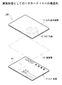
図1は、本発明の実施形態としての製造方法によって形成されるIDカード100の構造例を示す斜視図である。
【0018】
この実施形態では、顔画像や文字記録画像が形成された面のカード基板上に透明性の硬化型保護部材を設けて保護する場合に、この部材の膜厚や、加工温度、接着剤の厚みなどを最適に規定して、保護部材形成時における加工性を悪化させることなく、しかも、カード基板上の表面保護性に優れ、かつ、耐擦過性(耐摩耗性)に優れたIDカードを提供できるようにしたものである。
【0019】
この発明に係るIDカード100は、身分証明書、パスポート、外国人登録証、図書館利用カード、キャッシュカード、クレジットカード、自動車免許証等の免許証類、従業者証、社員証、会員証、医療カード及び学生証などに適用するものである。IDカード100は図1に示すカード基板11を有しており、カード使用者の個人情報などが書き込まれる。個人情報とは、住所、氏名、生年月日、本籍地、従業者証の発行年月日及び有効期限等をいう。IDカード100には内部にICチップ及びアンテナを内蔵した非接触式の電子カードも含まれる。電子カードの場合には個人情報がICチップなどに記録される。
【0020】
この例ではカード基板11に顔画像や文字記録画像などの記録画像が形成される。IDカード100としての従業者証は、図1において、例えば、縦の長さが6cm程度で、横の長さが9cm程度で、厚みが0.5〜1.0mm程度を有している。その従業者証の顔画像形成領域P1にはカード使用者の顔画像が形成され、その他の領域には文字記録情報などが印刷される。文字記録情報は、例えば「○○○従業者証」、「個人認識番号」、「氏名」、「発行日」・・・などである。
【0021】
このカード基板11上には透明性でシート状の硬化型保護層(以下硬化型保護部材ともいう)12が設けられ、カード基板表面を覆うように保護される。硬化型保護部材12には紫外線硬化層及び接着層を有した硬化型転写箔部材が使用される。この種の硬化型転写箔部材が使用されるのは、この紫外線硬化型転写箔などがガラスのような性質を有していることから、外部からカード基板上に衝撃力が加わった場合でも、その際の摩擦による擦り傷から顔画像などを保護できるからである。
【0022】
この例では硬化型保護層12の基板面側には凹凸状の模様を成すホログラム像13が設けられる。ホログラム像13は例えば円形の中に六角星形を成した特殊な画像である。もちろん、ホログラム像13は六角星形のような幾何学模様に限られることはなく、模倣され難い形状であればどんな形状であっても構わない。
【0023】
このカード基板11と硬化型保護層12とは接着層14を介して張り合わされている。接着層14には、ホットメルト樹脂や樹脂軟化点の温度が130℃程度又はそれよりも少し高い温度の熱溶融樹脂をフィルム状に形成したものを使用するとよい。
【0024】
図2は、IDカード100としての顔画像入りカード101の積層構造例を示す断面図である。図2に示す顔画像入りカード101上には膜厚Thの硬化型保護層(画像保護層)12を有している。ここで、図2に示す硬化型保護層12の膜厚をThとしたとき、
0.5μm≦Th≦5.0μm
に規定される。硬化型保護部材12や支持体16の材質にもよるが、好ましくは3μmが理想値である。
【0025】
この膜厚Thを規定したのは、硬化型保護部材12の転写時の加工性及びカード完成後の表面保護性の両立を図るためである。硬化型保護層12の膜厚を0.5μm乃至5.0μmに規定することによって、IDカード100の端部において、いわゆるバリと呼ばれる目視可能な凹凸状の部材残留片の発生が抑えられる。また、カード完成後の記録画像上をある程度強く擦っても、硬化型保護層12上の傷の発生が抑えられ、その記録画像上に目視可能な傷跡が残ることがない。
【0026】
この硬化型保護層12は光硬化性や熱硬化性等を利用してカード基板上に硬化型保護部材を形成するものである。詳しくは、特開昭54−92404号、同56−144994号、同56−148580号、同56−155789号、同56−166090号、同59−49993号、同59−76290号、同59−103788号、同60−112441号、同60−239277号、同60−254175号、同62−83177号、同63−293099号、特開平1−18698号、同1−80598号、同1−180400号、同2−93893号、同3−121884号、同3−45391号、同3−065400号、同4−69286号、W91/1223等に保護部材の形成方法が記載されている。
【0027】
この種の保護部材により形成される硬化型保護層12の硬化時期は、転写前、転写後のいずれでもよいが、好ましくは転写前であり、予め転写前に硬化型保護層12を硬化して置けば、転写後の硬化工程を省略することができる。
【0028】
また、硬化型保護部材12の硬度は鉛筆硬度で示すとHB以上である。ここで、鉛筆硬度とはJIS K5400による鉛筆(6B〜B、HB、H、2H〜6H)のカーボン芯の硬度をいう。硬化型保護部材12の最も硬い層は弾性率350kg/mm2以上、破断伸度20%以下が好ましく、更に好ましくは弾性率400kg/mm2以上、破断伸度15%以下がより好ましい。この例で硬化型保護層12の裏面にはホログラム形成層3が形成され、ホログラム像13が形成されている。この形成方法については図10〜図12において説明をする。
【0029】
更に、カード基板11と硬化型保護層12とは接着層14によって熱接着されている。ここで、図2に示す接着層14の厚みをtとしたとき、
0.1μm<t<20μm
に規定される。このように厚みtを規定すると、接着力不足を原因とするカード基板11から硬化型保護層12が剥離することが防止できる。
【0030】
図2示すカード基板11は下層から順に筆記層11A、クッション層11B、支持体11C、クッション層11D、熱昇華型受像層11Eなどが積層されて成る。この例で接着層14には、一般にBステージエポキシと呼ばれるゲル状のエポキシ樹脂が用いられる。ホットメルト樹脂としては、Henkel社製のマクロメルトシリーズなどのポリアミド系ホットメルト樹脂や、シェル化学社製のカルフレックスTR及びクイントンシリーズ、旭化成社製のタフプレン、Firestone Synthetic Rubber and Latex社製のタフデン、Phillips Petroleum社製のソルプレン400シリーズなどの熱可逆性エラストマー系のホットメルト樹脂が好ましい。
【0031】
また、住友化学社製のスミチックや、チッソ石油化学社製のビスタック、三菱油化製のユカタック、Henkel社製のマクロメルトシリーズ、三井石油化学社製のタフマー、宇部レキセン社製のAPAO、イーストマンケミカル社製のイーストマンボンド、ハーキュレス社製のA−FAXなどのポリオレフィン系ホットメルト樹脂が好ましく、更に、住友スリーエム社製のTE030及びTE100や、日立化成ポリマー社製のハイボン4820、鐘紡エヌエスシー社製のボンドマスター170シリーズ、Henkel社製のMacroplast QR3460などのホットメルト樹脂が好ましく、エチレン・酢酸ビニル共重合体系のホットメルト樹脂や、ポリエステル系のホットメルト樹脂などが好ましい。ホットメルト樹脂は接着後に湿気を吸って硬化する性質を有している。
【0032】
このカード完成後のカード基板11又はその一部の軟化点は130℃以下に規定される。この軟化点を130℃以下としたは、身分証明書、パスポート、外国人登録証、図書館利用カード、キャッシュカード、クレジットカード、自動車免許証等の免許証類、従業者証、社員証、会員証、医療カード及び学生証などが炎天下の駐車中の車内に置かれることを想定した場合に、車内温度が90℃に到達することが経験上見い出され、ホットメルト樹脂の熱溶融によってカード基板11から硬化型保護部材12が剥離することを防止するためである。
【0033】
図3A及び図3Bは、他の顔画像入りカード102及び103の積層構造例を示す断面図である。図3Aに示す他の顔画像入りカード102はカード基板11を有している。このカード基板11には記録画像が形成され、この記録画像形成面側上を覆うように透明性の硬化型保護層12が設けられる。
【0034】
この顔画像入りカード102は所定膜厚の同種類又は異種類の複数の硬化型保護部材12を積層した多重構造を有している。例えば、顔画像入りカード102はカード基板11上に同種類の所定膜厚の二層の硬化型保護部材12A及び12Bと、二層の偽変造防止箔とが積層されて成る。この例でも、硬化型保護部材12A及び12Bには顔画像入りカード101と同様な硬化型転写箔が使用される。
【0035】
この例では、一層の硬化型保護層12A又は12Bの膜厚をThとしたとき、0.5μm≦Th≦5.0μmに規定される。この膜厚Thを規定したのは、硬化型保護部材12A及び12Bの転写時の加工性及びカード完成後の表面保護性の両立を図るためである。硬化型保護部材12A及び12Bを二回に分けて転写することにより、バリの発生がより一層抑えられる。
【0036】
これと共に、カード完成後の表面保護性が図3Bに示す他の顔画像入りカード103に比べて向上する。図3Bに示す顔画像入りカード103はホログラム像13の偽変造防止箔13A及び硬化型保護層12を各々一層にずつ形成したものである。多重にするものは硬化型保護層12のみに限られることはなく、所定膜厚の硬化型保護層12と偽変造防止箔13Aとを組み合わせて多層にしてもよい。
【0037】
このように、単一の硬化型保護層12を設けた場合に比べて、カード表面に形成された顔画像や文字記録画像などをより一層強固に保護することができる。しかも、単一種類の硬化型保護部材12を厚めに設けた場合に比べてカード基板11上の表面保護性を低下させることなく、その硬化型保護部材12の転写時に、硬化型保護層12のカード外周端部でのバリの発生を極めて少なくすることができる。これにより、耐擦過性に優れたIDカード100を提供できる。
【0038】
図4Aは、IDカード100上の硬化型保護層12の平面、及び、図4Bはその断面の構成例(その1)を示すイメージ図であり、図5Aは、IDカード100上の硬化型保護層12の平面、及び、図5Bはその断面の構成例(その2)を示すイメージ図である。この例でも、硬化型保護部材12A及び12Bには顔画像入りカード101と同様な硬化型転写箔が使用される。
【0039】
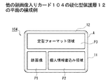
図4Aに示すIDカード100は枠線や枠組み線などの定型フォーマットを含む記録画像がカード基板11上に形成されるものである。この例で、図4Aに示す記録画像が形成される領域(以下画像形成領域という)Bは、図1に示したIDカード100の大きさを基準にすると、カード基板11の外周縁部から内側にβ=1.5mm以上後退した部位に配置される。このカード基板11上にも、記録画像形成面1上を覆うように透明性の硬化型保護層12が設けられる。ここで、記録画像形成面側のカード基板領域をAとし、画像形成領域をBとし、硬化型保護層12が設けられる領域(以下画像保護領域という)をCとし、硬化型保護層12がカード基板領域Aを越えて覆われた際のはみ出し領域をαとしたときに、(1)式、すなわち、
A+α⊇C⊃B・・・・(1)
なる関係を有するようになされる。このはみ出し領域αに関しては、図5A及び図5Bに示すカード基板11の外周縁部から外側へはみ出した硬化型保護層12のはみ出し距離をδとしたとき、
0≦δ≦300μm
に規定される。このように規定すると、少なくとも画像形成領域Bが硬化型保護層12によって保護され、この画像形成領域Bはもとより、図5Aに示すようにカード基板領域Aを越えて硬化型保護層12が覆われた場合にも、図5Bに示すはみ出し距離δが300μm以内に抑えられる。これにより、硬化型保護層12の転写時の外バリの発生による問題の発生が抑えられ、カード基板11上の表面保護性に優れ、かつ、耐擦過性(耐摩耗性)に優れたIDカード100を提供できる。
【0040】
なお、硬化型保護部材12の転写時のカード外周端部から画像形成領域B側へ硬化型保護層12が、はみ出す内バリに関しては、図1のIDカード100の例で図4Aに示すカード基板11の外周縁部と画像保護領域Cの外周縁部との間の距離をγとしたとき、
0mm≦γ≦0.8mm
に規定される。このように規定すると、画像形成領域Bが硬化型保護層12によって保護され、硬化型保護層12の転写時の内バリの発生による問題の発生が抑えられ、カード基板11上の表面保護性に優れ、かつ、耐擦過性(耐摩耗性)に優れたIDカード100を提供できる。
【0041】
この例では、図4Bに示す画像形成領域Bを取り囲む外周領域Dに厚み調整用の硬化型転写層15が設けられる。この硬化型転写層15を設けることによって画像形成領域Bの厚みと同等にできるので、段差の無いIDカード100を構成できる。
【0042】
図6は、他の顔画像入りカード105の硬化型保護層12の平面の構成例を示すイメージ図である。この顔画像入りカード105では、図4A及び図5Aに示したIDカード100のように定型フォーマットがカード基板11の外周部に沿って設けられていない。IDカード100に印刷される定型フォーマットは、必ずしも、図4A及び図5Aに示したようにカード基板11の外周部に沿って設ける必要はない。
【0043】
IDカード100の用途によっては、図6に示すカード基板領域Aに、顔画像形成領域P1、個人情報書き込み領域P2及び定型フォーマット領域P3が分散して割り当てられる。この場合にも、上述の(1)式に示したA+α⊇C⊃Bの関係式、及び、図4Aに示したカード基板11の外周縁部と画像保護領域Cの外周縁部との間の距離γに関して、0mm≦γ≦0.8mmに規定される。この際の画像形成領域Bには顔画像形成領域P1、個人情報書き込み領域P2及び定型フォーマット領域P3が含まれる。
【0044】
このように規定すると、顔画像形成領域P1、個人情報書き込み領域P2及び定型フォーマット領域P3が硬化型保護層12によって保護され、硬化型保護層12の転写時の外バリ及び内バリの発生の問題の発生が抑えられ、カード基板11上の表面保護性に優れ、かつ、耐擦過性(耐摩耗性)に優れた顔画像入りカード105を提供できる。
【0045】
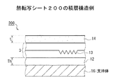
(2) 熱転写シート
図7は、実施形態としての熱転写シート200の積層構造例を示す断面図である。この実施形態では硬化型保護部材12が、予めカード基板11の外形状を成す大きさに画定されるものである。
【0046】
図7に示す熱転写シート200は支持体16を有している。この支持体16上には所定膜厚の硬化型保護部材12が設けられる。この硬化型保護部材12には紫外線硬化層及び偽変造防止箔が使用される。ここで、図7に示す硬化型保護層12の膜厚をThとしたとき、
0.5μm≦Th≦5.0μm
に規定される。この硬化型保護部材12の上面にはホログラム形成層3が形成され、ホログラム像13が形成されている。ホログラム形成層3上には所定の膜厚の接着層14が形成されている。ここで、図7に示す接着層14の厚みをtとしたとき、
0.1μm<t<20μm
に規定される。これらの規定理由については上述した通りである。
【0047】
図8は熱転写シート200のハーフカット例を示す概念図である。この例では、カード基板11の外形状を模写した切り込みが硬化型保護部材12に施される。この切り込みは、接着層14、ホログラム形成層3及び硬化型保護層12に施され、支持体16には形成されない。支持体16の本来の支持機能を損なうからである。
【0048】
この切り込みはカード基板外形状を模写したカッターなどを使用してシャープに形成され、図8に示す熱転写シート200の硬化型保護部材12に対して実際のカード基板11よりも小さい寸法で施される。これは外バリ及び内バリを無くすためである。これにより、カード基板11の外形状を成す大きさに硬化型保護部材12を画定することができる。
【0049】
このように、本実施形態に係る熱転写シート200によれば、支持体16上に設けられた所定膜厚の硬化型保護部材12が予め被接着物となるカード基板11の外形状を成す大きさに画定されているので、その転写時に、硬化型保護層12のカード外周端部でのバリの発生を極めて少なくすることができる。これにより、耐擦過性(耐摩耗性)に優れたIDカード100を歩留まり良くかつ再現性良く製造することができる。
【0050】
(3) 熱転写シートの製造方法
図9A〜図9Cは、実施形態としての熱転写シート200の形成例を示す工程図である。この実施形態では、カード基板11と同じ外形状を成す大きさに画定した剥離可能な所定膜厚の接着剤付きの硬化型保護部材12をシート状の支持体16に形成する場合を想定する。また、熱転写シート200の幅はカード基板11の幅よりも、そのカード基板の両側に余裕が保てるように幅広く形成する。幅広く形成することにより転写ミスを防げる。
【0051】
まず、図9Aにおいて、膜厚Thが、0.5μm≦Th≦5.0μm程度となる硬化型保護部材12を支持対16上に形成する。この支持体16には数十μm程度のポリエチレンフィルムなどを使用する。硬化型保護部材12にはエポキシアクリレート、ヒロキシアクリレート、テトラヒドロフルアクリレート及び光重合開始剤ベンゾフェノンなどの紫外線硬化性組成物が使用される。これらの紫外線硬化部材は支持体16上にワイヤーバーで塗布され、その後、所定のエネルギーの紫外線が照射される。
【0052】
その後、図9Bにおいて、硬化型保護部材12上にホログラム像付きのホログラム形成層3を形成する。例えば、常用の方法により、硬化型保護部材12上の所定の位置に反射型ホログラム形成層3を形成する。反射型ホログラム形成層3は硬化型保護部材12上に樹脂層3Aを形成した後に金属蒸着層3Bを施す。これにより、カード基板転写時には硬化型保護層12下に偽変造防止箔が形成される。偽変造防止を目的とした印刷は、IDカード100に転写した状態において、硬化保護層12とカード基板11との間に存在することが好ましい。
【0053】
偽変造防止を目的とした印刷には、ホログラムの他に、細紋、透かし、{反射型ビーズ、紫外線吸収剤、赤外線吸収剤、蛍光増白剤}から選ばれる少なくとも、1つを含有する組成物により形成された印刷層、磁気記録層、バーコードの公知の方法を挙げることができるが、単独あるいはこれらの2種以上を併用してもよい。例えば反射型ビーズを用いる方法については特開平6−507737号に記載されている。
【0054】
その後、図9Cにおいて、ホログラム形成層3上に接着部材を塗布して接着層14を形成する。接着部材には反応型ホットメルト樹脂や、ウレタン変成オレフィン樹脂などを使用する。この際に接着層14の厚みtが0.1μm<t<20μmとなるように接着部材をワイヤーバーで塗布する。その後、カード基板外形状を模写したカッター17などを使用して、切り込みを入れる。これにより、鉛筆硬度HB以上の接着剤付きの熱転写シート200が完成する。
【0055】
このように、本発明の熱転写シートの製造方法によれば、カード基板11の外形状を成す大きさに画定した所定膜厚の硬化型保護部材12がシート状の支持体16上に形成されるので、硬化型保護部材12の転写時に、カード基板11の硬化型保護層12からカード外周端部へはみ出す凹凸状の部材残留片の発生を極めて少なくすることができる。
【0056】
図10Aは、熱転写シート200としてのホットスタンプフィルム32の形成工程例を示す斜視図、図10Bは、ホログラム像形成時の構成例を示す一部断面図である。ホットスタンプフィルム32は枚葉状の熱転写シート200として使用するものである。ホットスタンプフィルム32は膜厚Thが、0.5μm≦Th≦5.0μm程度となる硬化型保護部材12から成る。硬化型保護部材12は紫外線硬化層及び接着層を有した転写箔である。例えばホットスタンプフィルム32はIDカード100の大きさとほぼ同じ大きさ、又は、それよりも小さめに予め裁断したものを図10Aに示すベースフィルム31に貼付することにより形成される。
【0057】
この場合にも、上述の(1)式に示したA+α・C・Bの関係式、及び、図4Aに示したカード基板11の外周縁部と画像保護領域Cの外周縁部との間の距離γに関して、0mm≦γ≦0.8mmに規定される。このベースフィルム31はラミネットコーティング工程時に剥離される。
【0058】
この例では、ベースフィルム(支持体)31の両端には位置決め用の開孔部37が一定間隔で設けられ、この開孔部37を使用してホログラム像13などが形成される。この開孔部37はカード基板11とホットスタンプフィルム32などの熱転写シート200との位置決めのときにも使用される。
【0059】
例えば、図10Bに示すホログラム像作成手段34を使用してホログラム像13を形成するときに、ホログラム像作成手段34による金型35をホットスタンプフィルム32にスタンプを押すが如く押下して凹凸状の六角星形模様などを形成する。これにより、ホットスタンプフィルム32に再現性良くホログラム像13を象ることができる。
【0060】
この際に、ホログラム像作成手段34からベースフィルム31の両側の開孔部37に位置合わせ用のピン38A,38Bが挿入され、ベースフィルム31上のホットスタンプフィルム32の所定位置に金型35を押下させることができる。この際の金型35に関しては、カード発行機関の認証となる場合もある。このような認証を伴う熱転写シート200を以後、認証保護シートともいう。その後、ホログラム像13を有したベースフィルム31をロール状に巻き取る。この例ではロール状に限られることはなく、1枚のIDカード100の大きさに見合うようにベースフィルム31を切断し、ホログラム像を含んだベースフィルム31をカットシート状にストックさせて梱包するようにしてもよい。
【0061】
図11Aは、熱転写シート200としてのラミネートフィルム33の形成工程例(その1)を示す斜視図、図11Bは、ホログラム像形成時の構成例を示す一部断面図である。図12はそのラミネートフィルム33の形成工程例(その2)を示す斜視図である。この例では熱転写シート200となる図11Aに示す長尺シート状のラミネートフィルム33に、図11Bに示すホログラム像作成手段34の金型35を押下して凹凸状の六角星形模様などを形成するものである。ラミネートフィルム33は膜厚Thが、0.5μm≦Th≦5.0μm程度となる硬化型保護部材12から成る。硬化型保護部材12は紫外線硬化層及び接着層を有した転写箔である。
【0062】
もちろん、ホログラム像13を形成する面はIDカード100の表面に当接させる側である。この例でホットスタンプフィルム32及びラミネートフィルム33のホログラム形成層3上には膜厚tが0.1μm<t<20μm程度となる接着シート14が、ホログラム像13を形成した面に張り合わされる。この接着シート14はいわゆる両面接着テープのようにその両面が接着性を有するので、その片側は図示しない剥離容易な紙シートによって接着性が保持されている。
【0063】
この接着シート14の張り合わせ時には、加熱ローラ36A、36Bを使用してラミネートフィルム33などが加熱されながら加圧貼付される。その後、ホログラム像13を有したラミネートフィルム33がロール状に巻き取られる。このロール状のラミネートフィルム33はカートリッジに収容するか又は包装するようになされる。
【0064】
これらの熱転写シート200をカートリッジなどに収容すると、熱転写装置における交換作業が簡単に行えるようになり、作業負担が軽減され、作業能率が向上する。これらのホットスタンプフィルム32及びラミネートフィルム33をカートリッジから繰り出すことにより、カード基板11上を透明性の硬化型保護層12保護することができる。
【0065】
(4) IDカードの製造方法
図13A〜図13Cは、実施形態としてのIDカード100の形成工程例を示す断面図である。図14は、カード基板11と熱転写シート200との位置合わせ例を示す概念図である。
【0066】
この実施形態では、予めカード基板11に記録画像が形成され、その後、記録画像が形成された面のカード基板11上にほぼ透明性の硬化型保護部材12を転写することにより、そのカード基板11上に0.5μm乃至5.0μmに規定される膜厚の硬化型保護層12を形成することを前提とする。この透明性の硬化型保護部材12に関しては上述した接着剤付きの熱転写シート200が予め準備され、この硬化型保護部材12の最適な転写条件は、「(7)実施例」で説明する本発明者らの実験例によって見出されているものとする。
【0067】
これらを前提として、図13Aにおいて、硬化型保護部材12をカード基板11上に熱を加えて当接する。この際に、硬化型保護部材12をカード基板11上に当接する加圧力をFcとしたとき、
0g<Fc<20kg
に規定される。Fc>20kgでは硬化型保護部材12が潰れてしまい、剥離の際の内バリ及び外バリの発生原因となる。この当接の際の加工温度(以下転写温度ともいう)をTxとしたとき、
90℃<Tx<250℃
に規定される。
【0068】
このように転写温度Txを規定したのは、Tx<90℃及びTx>250℃では、熱転写シート200及びカード基板11が共に移動される条件下で、硬化型保護部材12の剥離性が悪くなり、内バリ及び外バリの発生原因となるからである。当接時の転写温度Txを90℃<Tx<250℃に規定することにより、カード完成後の熱溶融によるカード基板11から硬化型保護部材12が剥離することを防止できる。接着力不足によるカード基板11から硬化型保護部材12が剥離することが防止できる。
【0069】
この例では、熱転写シート200には予め図14に示す位置決め用の開孔部37が設けられ、この開孔部37を使用してカード基板11と熱転写シート200の切り込みとが位置合わせされる。例えば、図示しない熱転写装置から熱転写シート200の開孔部37に位置合わせ用のピン39A,39Bが挿入される。カード基板11の外周端部に対してそのカード基板形状に切り込みを入れられた硬化型保護部材12とが位置決めされる。これにより、カード基板11上にその広さ分の硬化型保護部材12を当接することができる。
【0070】
その後、図13Bにおいて、熱転写シート200又はカード基板11を予め見出された転写条件に基づいて一定方向に移動する。実際の熱転写装置ではスループットを上げるために、熱転写シート200及びカード基板11を同時に一定方向に移動する方式が採られるためである。この例で後者を採る場合には、カード基板11も移動状態にあって、熱転写シート(支持体16)200を一定方向に引く力を張力Faとしたとき、
200g<Fa<1.5kg
に規定される。硬化型保護部材12や支持体16の材質にもよるが、好ましくは600gが理想値である。
【0071】
このように張力Faを規定したのは、Fa<200g及びFa>1.5kgでは熱転写シート200及びカード基板11が共に移動される条件下で、硬化型保護部材12の剥離性が悪くなり、内バリ及び外バリの発生原因となるからである。移動時の張力Faを200g<Fa<1.5kgに規定することにより、剥離時の内バリや外バリの発生を抑えることができる。その際には、熱転写シート200の移動速度をV1とし、カード基板11の移動速度をV2としたとき、
V1<V2
に規定される。
【0072】
例えば、熱転写シート200の移動速度V1に対するカード基板11の移動速度V2は、
1.02・V1<V2<1.4・V1
に規定される。つまり、熱転写シート200の移動速度V1と、カード基板11の移動速度V2との速度差Vεを2%乃至40%になるように規定する。このように速度差Vεを規定したのは、Vε<2%及びVε>40%では熱転写シート200及びカード基板11が共に移動される条件下で、硬化型保護部材12の剥離性が悪くなり、内バリ及び外バリの発生原因となるからである。これらの移動時の速度差Vεを2%<Vε<40%に規定することにより、剥離時の内バリや外バリの発生を抑えることができる。例えば、カード基板11の終端部において、熱転写シート200から硬化型保護部材12を瞬時に切断することができる。
【0073】
この例で熱転写シート200及びカード基板11の移動状態のときに、支持体16の剥離に先立って、後述するカートリッジでの記載中にあるような機構を用いて、カード基板11の外周形状の大きさになるように折り曲げ機構などによって硬化型保護部材12に折り目を施してカード基板11の外周形状の大きさになるように被転写領域を画定して置いてもよい。
【0074】
その後、図13Cにおいて、カード基板11を覆う大きさの硬化型保護部材12を支持体16から剥離してそのカード基板11上に硬化型保護層12を形成する。この例では、支持体16と硬化型保護層12の接着力をFbとしたとき、
0.5g/cm<Fb<25g/cm
に規定される。硬化型保護部材12や支持体16の材質にもよるが、好ましくは10gが理想値である。ここで、接着力Fbとは粘着テープ(ニチバン#405など)を硬化型保護層12に貼り付けて剥離角θ=180°で剥離を行うときの単位センチメートル幅当たりの剥離力をいう。
【0075】
このように接着力Fbを規定したのは、Fb<0.5g/cm及びFb>25g/cmでは、熱転写シート200及びカード基板11が共に移動される条件下で、硬化型保護部材12の剥離性が悪くなり、内バリ及び外バリの発生原因となるからである。この剥離時の接着力Fbを0.5g/cm<Fb<25g/cmに規定することにより、内バリや外バリの発生を抑えることができる。
【0076】
この例では、硬化型保護部材12が転写された後の熱転写シート200、つまり、支持体16をカード基板11上から一定方向に引く角度を剥離角θとしたとき、
10°<θ<150°
に規定される。硬化型保護部材12や支持体16の材質にもよるが、好ましくは剥離角θは75°が理想値である。
【0077】
このように剥離角θを規定したのは、θ<10°及びθ>150°では、熱転写シート200及びカード基板11が共に移動される条件下で、硬化型保護部材12の剥離性が悪くなり、内バリ及び外バリの発生原因となるからである。もちろん、カード基板11の先端部と終端部で硬化型保護部材12の剥離角θを変えてもよい。
【0078】
この剥離角θを10°<θ<150°に規定することによって、支持体16からカード基板11へ硬化型保護部材12が内バリ及び外バリを伴うことなく、かつ、再現性良く転写できる。これにより、硬化型保護層12の接着面側に、偽変造防止を目的とした像又は形状が施され、顔画像や文字記録画像を透明性の硬化型保護層12により保護したIDカード100が完成する。
【0079】
なお、カード基板11を覆う硬化型保護部材12は一層に限られることはなく、そのカード基板11と同じ大きさの他の硬化型保護部材12をもう一度、熱転写シート200から剥離して同一カード基板11上に二以上を積層してもよい。つまり、同一カード基板11上に所定膜厚の同種類又は異種類の硬化型保護部材12を多重に形成する。
【0080】
また、カード基板11へ硬化型保護層12を転写する際に、そのカード基板11の搬送方向における後端が硬化型保護部材12から離間する直前に、その後端を硬化型保護部材12から離れる方向に撓ませるようにするとよい。これは、支持体16から硬化型保護部材12が剥離する際に、カード基板11の後端エッジに沿って硬化型保護部材12が切断し易くなり、硬化型保護層12のカード外端部でのバリの発生を無くせるからである。
【0081】
更に、支持体16から硬化型保護部材12が徐々に剥離され、その硬化型保護部材12が徐々に転写されたカード部分を、この剥離中に、上下のローラーや、ローラーとステージなどの平面で挟持するようにするとよい。これは剥離が済んだカード基板11の振動を防止できると共に、この振動を抑えることにより、カード側端部でのバリの発生が抑えられるからである。
【0082】
このように、本発明のIDカード100の製造方法によれば、予め見出された硬化型保護部材12の膜厚や、カード基板11の転写温度、熱転写シート200の接着剤14の厚みtなどの最適な転写条件に基づいて、膜厚が0.5μm乃至5.0μmに規定される硬化型保護層12がカード基板11上に形成されるので、カード表面に形成された顔画像や文字記録画像などを良好に保護することができる。しかも、カード基板11上の表面保護性を低下させることなく、硬化型保護層12のカード外端部でのバリの発生を無くすことができる。
【0083】
また、本実施形態によれば、剥離可能な接着剤付きの硬化型保護部材12が形成された支持体16からその硬化型保護部材12を剥離して同一カード基板11上に二以上積層されるので、単一種類の硬化型保護部材12を1回で厚めに形成する場合に比べてカード基板11上の表面保護性を低下させることなく、硬化型保護層12のカード外周端部でのバリの発生を極めて少なくすることができる。これにより、耐擦過性(耐摩耗性)に優れたIDカード100を歩留まり良く、かつ、再現性良く製造することができる。
【0084】
(5) IDカードの製造装置
図15は、実施形態としての製造方法が適用されるIDカードの製造装置300の構成例を示す概念図である。この実施形態では、当該製造装置300に関して画像形成装置301及び熱転写装置400が分離して構成され、枚葉状のカード基板11に顔画像や文字記録情報などを形成した後に、熱転写シート200を転写する場合を想定する。
【0085】
この発明のIDカードの製造装置300は、カード基板11上に透明性の硬化型保護部材12を転写して身分証明書、パスポート、外国人登録証、図書館利用カード、キャッシュカード、クレジットカード、自動車免許証等の免許証類、従業者証、社員証、会員証、医療カード及び学生証などのIDカード100を製造するものである。
【0086】
図15に示すIDカードの製造装置300は画像形成装置(画像形成手段)301及び熱転写装置302を有している。画像形成装置301は搬送ベルト装置41を有している。搬送ベルト装置41の一端上部には、生カード供給部42が設けられている。生カード供給部42にはカード使用者の個人情報を書き込むために予め枚葉状にカットされた複数のカード基板11が、顔写真を現像する面を上に向けてストックされている。
【0087】
カード基板11の裏面にはサインパネルや、運転免許証の筆記層などが設けられる場合もある。この例では、カード基板11が1枚ずつ生カード供給部42から搬送ベルト装置41へ投下するように自動供給される。
【0088】
その自動供給後の搬送ベルト装置41上のカード基板11は左側から右側に搬送される。搬送ベルト装置41上には画像形成部(プリンタ)43が設けられ、カード基板11が左側から右側に移動される間に、そのカード基板11の顔画像形成領域P1にカード使用者の顔写真が現像されたり、その他の文字記録領域にはカード使用者の氏名や、カード発行日などが記録される。この際の画像形成手段には、昇華型感熱転写記録方式、ハロゲン化銀カラー写真方式、電子写真方式、インクジェット方式等が使用される。
【0089】
この画像形成装置301において、カード基板11が電子カード構造を採るときは、画像形成部43の他に情報書き込み部44及び情報チェック部48が設けられる。例えば、搬送ベルト装置41の下流側に波線で示す情報書き込み部44を設け、カード使用者の個人情報がカード基板11内のICチップなどに書き込まれる。情報書き込み部44において、個人情報の書き込むときに、磁気コードや、バーコード等などを併用してもよい。
【0090】
また、情報書き込み部44の下流側には第1の駆動ローラ45を挟んで画像チェック部46が設けられ、画像形成部43で形成された使用者の顔写真や、氏名、カード発行日などが誤っていないかチェックされる。上述の情報書き込み部44を設けた場合には、更に、画像チェック部46の下流側に第2の駆動ローラ47を挟んで情報チェック部48を設け、情報書き込み部44で書き込まれた個人情報が誤っていないかチェックしてもよい。この情報チェック部48の下流側には図示しないカード排出口が設けられ、顔画像などが形成されたカード基板11が排出される。
【0091】
この画像形成装置301には熱転写装置(転写手段)302が組み合わされ、顔画像入りのカード基板11上に熱転写シート200から剥離した透明性の硬化型保護部材12が熱転写される。熱転写装置302にはホットスタンプ装置などが使用される。この熱転写装置302に搬送手段としての搬送ベルト装置49が設けられ、硬化型保護部材12が当接されたカード基板11を位置規制しながら一定方向に搬送される。この例では個人情報が書き込まれたカード基板11が左側から右側に搬送される。搬送ベルト装置49上には熱転写シート用のカートリッジ(以下転写用カートリッジという)400が設けられている。転写用カートリッジ400には部材供給手段としての熱転写シート用のコア(以下転写箔コアという)51が設けられ、カード基板11に当接させる側に、例えば、凹凸状の六角星形模様から成るホログラム像13を有したテープ状で接着剤付きの熱転写シート200が供給される。
【0092】
この例で熱転写シート200にはテープ状のラミネートフィルム33などをロール状に巻き込んだものが使用され、この熱転写シート200は予め転写用カートリッジ400内に巻装され、転写用カートリッジ400が熱転写装置に装填される。もちろん、そのラミネートフィルム33は一方の面にホログラム像13を有し、かつ、同じ面に接着層14を有している。
【0093】
また、熱転写シート200はラミネートフィルム33に限定されることはなく、ホットスタンプフィルム32をロール状に巻き取ったもの、又は、ホットスタンプフィルム32をカットシート状に積層されたものを使用してもよい。ホットスタンプフィルム32には、一方の面にホログラム像13を有し、かつ、同じ面に接着層14を有したものを使用する。
【0094】
転写用カートリッジ400には当接手段(貼合手段)としての真空熱プレス装置52が設けられ、画像形成装置301から排出されたカード基板11に対して転写箔コア51からの熱転写シート200が当接され、そのカード基板11とその熱転写シート200の硬化型保護部材12とが接着層14を介して張り合わされる。この際に、接着層14上の紙シートは剥離され、カス紙として巻き取られる。
【0095】
この真空熱プレス装置52は搬送路上に配置された平型のプレス部を有しており、熱転写シート200の上方から所定の圧力が加えられる。そのために、プレス部が上下方向に移動できるようになされている。このプレス部には電気ヒータ(図示せず)が設けられ、熱転写シート200及びカード基板11を所定の温度に加熱するようになされている。
【0096】
この例では接着層14の種類にもよるが加熱温度は90℃〜250℃程度であり、加熱時間は10秒〜120秒程度である。この接着層14は熱を加えると溶融し、それが冷えると固化するものである。熱転写シート200を加熱貼合する装置は真空熱プレス装置52に限られることはなく、通常のサーマルヘッドなどの熱プレスでも、ヒートローラー装置であってもよい。
【0097】
また、真空熱プレス装置52の下流側には冷却部53が設けられ、加熱貼合されたカード基板11が冷却される。これにより、画像形成装置301によって記録画像が形成された面のカード基板11上に、ほぼ0.5μm乃至5.0μmに規定される膜厚の透明性の硬化型保護層12を熱転写装置302によって転写することができる。
【0098】
次に、IDカードの製造装置300の動作を説明する。この例では1枚のカード基板11にロール状の熱転写シート200からカード基板11の大きさの硬化型保護部材12を剥離取って、カード基板11上に転写する場合を前提にして説明する。まず、生カード供給部42から1枚のカード基板11を取り出し、搬送ベルト装置41上で左側から右側にカード基板11を搬送する。この間に画像形成部43によってカード使用者の顔写真、氏名及び発行日等が記録される。その後、カード基板11の種類によって、例えば、電子カードのような場合には、情報書き込み部44によって使用者の個人情報がICチップに書き込まれる。磁気カード103の場合にはカード使用者の個人情報が磁気テープに書き込まれる。
【0099】
その後、駆動ローラ45によって情報書き込み部44から画像チェック部46へカード基板11が移動される。画像チェック部46ではカード使用者の顔写真、氏名及び発行日等の画像がチェックされる。もちろん、チェック結果で「良」のみのカード基板11を下流側に送るようにする。「不良」のカード基板11はピックアップするようになされる。その後、駆動ローラ47によって画像チェック部46から情報チェック部48へカード基板11が移動される。電子カードの場合には情報チェック部48でICチップ内の記憶情報がチェックされる。チェック結果が「良」のカード基板11が画像形成装置301から排出される。
【0100】
そして、顔画像入りカード基板11が熱転写装置302に移行されると、転写用カートリッジ400では、例えば、ホログラム像13を有したシート状の熱転写シート200が転写箔コア51から繰り出されて真空熱プレス装置52上のカード基板11に供給される。
【0101】
この真空熱プレス装置52では、カード基板面とホログラム像形成面とが所定の位置で対向するようにカード基板11と熱転写シート200とが位置合わせされると共に、そのカード基板11と熱転写シート200とが接着層14を介して加熱圧着される。その後、冷却部53でカード基板11が常温に至る程度に冷却される。
【0102】
なお、上述したカード基板11の搬送方向における後端が硬化型保護部材12から離間する直前に、その後端を硬化型保護部材12から離れる方向に撓ませるような機構やカードの振動防止用の機構は冷却部53の直前に設けるとよい。これにより、硬化型保護層12で保護されたホログラム像付きの顔画像入りのIDカード100が完成する。
【0103】
このように、本実施形態に係るIDカードの製造装置300によれば、画像形成装置301によってカード基板11に記録画像が形成されると、この記録画像が形成された面のカード基板11上に、熱転写装置302によってほぼ透明性の硬化型保護部材12が転写され、その膜厚が0.5μm乃至5.0μmに規定された硬化型保護層12がカード基板11上に形成される。
【0104】
従って、カード基板11上に硬化型保護層12を形成できるので、顔画像や文字記録画像などを保護することができる。しかも、カード基板11上の表面保護性を低下させることなく、硬化型保護層12のカード外端部でのバリの発生を無くすことができる。これにより、耐擦過性(耐摩耗性)に優れた顔画像入りのIDカード100を製造することができる。
【0105】
(6)熱転写シート用のカートリッジ
図16は、実施形態としての転写用カートリッジ400の構成例を示す斜視図である。この例では、転写用カートリッジ400の所定位置に剥離用の棒状体を取り付け、転写箔コア51から繰り出された熱転写シート200からカード基板11の外形状を成す大きさの硬化型保護部材12を剥離するようにして、この転写時に、カード基板11の外形状の大きさに見合う分の硬化型保護部材12のみを熱転写シート200から剥離できるようにすると共に、硬化型保護層12の外周端部でのバリの発生を低減できるようにしたものである。
【0106】
図16に示す転写用カートリッジ400は筐体としてコ字状のテープ収容部21を有している。テープ収容部21は上ハーフ21A及び下ハーフ21Bに分離可能な分割構造を有している。このテープ収容部21には部材供給部としてボビン状の転写箔コア51が可動自在に取り付けられ、接着剤付きの硬化型保護部材12を施したテープ状の熱転写シート200がコ字状部23へ繰り出される。
【0107】
この例でも、熱転写シート200には、紫外線硬化層を有した転写箔及び偽変造防止箔が設けられたもの、予めカード基板11の外形状を成す大きさに硬化型保護部材12が画定されたもの、その外形状を模写した切り込みが施されたもの、その際の切り込みが、実際のカード基板11よりも小さい寸法で施されたもの、及び、位置決め用の開孔部37が設けられたものが使用される。
【0108】
この転写用カートリッジ400の転写箔コア51への回転動力は熱転写装置302の本体部から供給される。この転写箔コア51は使用前の熱転写シート200が巻装された元巻きコア51A及び転写剥離後の支持体16を巻き取るための巻取りコア51Bを有している。テープ収容部21の所定位置には剥離用の棒状体として従動ローラ部22が取り付けられる。従動ローラ部22には硬化型保護部材12に負荷をかけない部材、例えば、外径が5mmφ程度の円筒状のプラスチィックを使用する。好ましくは熱転写シート200がカード基板11から剥離上がるとき、半径1.5mm以上のR形状に沿って移動することが望ましい。
【0109】
この従動ローラ部22は図16に示すテープ収容部21の側面下部であって、硬化型保護部材12の搬送方向(カード基板11の搬送方向)に対して熱転写シート200の移動方向を変える位置に設けられる。この例では従動ローラ部22がカード基板11の搬送方向に対して直交する方向に軸部22Aを有しており、この軸部22Aがテープ収容部21に可動自在に取り付けられる。この従動ローラ部22は硬化型保護部材12の接着面側がカード基板11に当接する状態において、熱転写シート200の移動によって回転され、元巻きコア51Aから繰り出された熱転写シート200からカード基板11の外形状を成す大きさの硬化型保護部材12を剥離するようになされる。
【0110】
この剥離用の棒状体は従動ローラ部22に限られることはなく、熱転写シート200に対して摩擦係数が小さな部材から成る非回転体であってもよい。例えば、非回転体にはステンレスや真鍮などの金属の丸棒のようなものを使用するとよい。剥離用の棒状体の摩擦抵抗を軽減することにより熱転写装置の巻き取りトルクを低減できる。
【0111】
更に、この例では、従動ローラ部22に隣接した位置のテープ収容部21の側面にカード浮き上り防止用の突出部としてカード浮上防止板24が設けられ、硬化型保護部材12の剥離時、特に、カード基板11の終端部の剥離時に、カード基板11の終端部の跳ね上がりを押さえ込むようになされる。この終端部の跳ね上がりを押さえ込むことにより、バリの発生を抑えることができる。
【0112】
図17は、熱転写装置302の一例となるホットスタンプ装置500の構成例を示す概念図である。この例ではホットスタンプ装置500に対して転写用カートリッジ400が脱着自在に取り付けられる。図17はホットスタンプ装置500に転写用カートリッジ400を装填した状態を示している。
【0113】
図17に示すホットスタンプ装置500にはカード給紙口25及びカード排出口26が設けられ、図15で説明した真空熱プレス装置52に代わって熱ローラ装置27が取り付けられる。この例では、硬化型保護部材12と支持体16との接着力Fbに関して0.5g/cm<Fb<25g/cmに規定された熱転写シート200が、転写用カートリッジ400の元巻きコア51Aから繰り出される。
【0114】
例えば、熱転写シート200はテープ収容部21内の案内部材28Aにガイドされて、コ字状部23から熱ローラ装置27の下部を通って従動ローラ部22を経由し、テープ収容部21内の他の案内部材28Bにガイドされて、巻取りコア51Bに至るようになされる。また、巻取りコア51Bによって熱転写シート200を巻き取る際の張力Faに関しては200g<Fa<1.5kgの範囲に規定される。
【0115】
従って、カード給紙口25からカード基板11を挿入すると、搬送ベルト装置49などにより、そのカード基板11が熱ローラ装置27下に移動される。この際に、巻取りコア51Bによる熱転写シート200の移動速度をV1とし、搬送ベルト装置49によるカード基板11の移動速度をV2としたとき、V1<V2に規定される。例えば、熱転写シート200の移動速度V1に対する搬送ベルト装置49によるカード基板11の移動速度V2は、1.02・V1<V2<1.4・V1に規定される。
【0116】
そして、カード基板面とホログラム像形成面とが所定の位置で対向するようにカード基板11と熱転写シート200とが位置合わせされると、熱ローラ装置27では、そのカード基板11と熱転写シート200とが接着層14を介して加熱圧着される。この際の加圧力Fcに関しては0g<Fc<20kgの範囲で、硬化型保護部材12が熱ローラ装置27によってカード基板11上に当接される。この際の転写温度Txに関しては90℃<Tx<250℃の範囲で、熱ローラ装置からカード基板11上の硬化型保護部材12へ熱が加えられる。
【0117】
その加熱の際にも、剥離用の従動ローラ部22が熱転写シート200の移動によって回転され、熱転写シート200の移動方向が、カード基板11の移動方向に対して剥離角θだけ変わるときに、この従動ローラ部22によって支持体16から硬化型保護部材12を剥離するようになされる。この剥離の際に、カード浮上防止板24によってカード基板11の終端部の跳ね上がりが押さえ込まれる。これにより、硬化型保護層12で保護された顔画像入りのIDカード100がカード排出口26から排出される。
【0118】
このように、本実施形態に係る転写用カートリッジ400によれば、接着剤付きの硬化型保護部材12を施した熱転写シート200が元巻きコア51Aから繰り出され、その硬化型保護部材12の接着面側がカード基板11に当接されると、テープ収容部21の側面に取り付けられた従動ローラ部22によって熱転写シート200からカード基板11の外形状を成す大きさの硬化型保護部材12が剥離される。
【0119】
従って、カード基板11の外形状の大きさに見合う分の硬化型保護部材12のみが熱転写シート200からカード基板11に容易に転写されるので、硬化型保護部材12の転写時に、カード基板11の硬化型保護層12から外周端部へはみ出す凹凸状のバリ(部材残留片)の発生を極めて少なくすることができる。これにより、支持体16から剥離した硬化型保護部材12によってカード基板11上の顔画像や文字記録画像などを良好に保護することができる。
【0120】
図18は、他の転写用カートリッジ401の構成例を示す断面図であり、そのテープ収容部21の剥離部付近を示している。この例では、カード基板11上から熱転写シート(支持体16)200を一定方向に引く角度を規定すると共に、カード終端浮上防止機構60を設けたものである。
【0121】
図18に示すカード終端浮上防止機構(当接手段)60は、剥離用の従動ローラ部22の他に押し当用の従動ローラ部29が、その従動ローラ部22に隣接して取り付けられ、カード基板11の上面に当てがわれる。上述した搬送ベルト装置49を構成する駆動ローラ49A及び49B間には押し当て板61が上下動可能な状態で取り付けられ、この従動ローラ部29に対してカード基板11を押し上げるように圧着される。例えば、押し当て板61には係合用のネジ62A,62Bなどが設けられ、このネジ部62Aにはバネ体63Aが嵌入され、ネジ部62Bにはバネ体63Bが嵌入され、常時、カード基板11を押し上げるように付勢されている。これにより、従動ローラ部29と押し当て板61とによりカード基板11と硬化型保護部材12とを密着させることができる。
【0122】
この例では、巻取りコア51Bによって熱転写シート(支持体16)200をカード基板11上から一定方向に引く角度、つまり、熱転写シート200とカード基板面とが成す角度を剥離角θとしたとき、
10°<θ<150°
に規定される。このように剥離角θを規定したのは、θ<10°及びθ>150°では、熱転写シート200及びカード基板11が共に移動される条件下で、硬化型保護部材12の剥離性が悪くなり、内バリ及び外バリの発生原因となるからである。好ましくは剥離角θを74.8°に設定するとよい。この剥離角θを74.8°に設定することによって、熱転写シート200からカード基板11へ硬化型保護部材12が内バリ及び外バリを伴うことなく、かつ、再現性良く転写できる。
【0123】
この例では、剥離用の従動ローラ部22に隣接して、剥離角設定用の従動ローラ部62が設けられ、剥離角度を自由に調整できるようになされている。もちろん、この従動ローラ部62は、非回転体の棒状体のようなものであってもよい。この転写用カートリッジ401には部材保持部63が設けられ、これらの従動ローラ部22、29および62の両端が可動自在に保持される。この部材保持部63は、テープ収容部21に対して可動自在に取り付けられる。
【0124】
例えば、剥離角θの調整が済んだ後には係合用のネジ64A、64Bによって部材保持部63がテープ収容部21に固定される。この構成によって、熱転写シート200から剥離した硬化型保護部材12によってカード基板11上の顔画像や文字記録画像などを良好に保護することができる。
【0125】
図19A及び図19Bは他の転写用カートリッジ402の折曲げ機構50の構成例を示す断面図である。この例では、転写用カートリッジ402側に折曲げ機構50が設けられ、硬化型保護部材12にカード基板両側端部を反映した折り目が施されるものである。
【0126】
図19Aに示す転写用カートリッジ402は部材変形手段としての弾性体圧力ローラー55を有している。弾性体圧力ローラー55には軟質ピンチローラなどを使用する。この弾性体圧力ローラー55は、少なくとも、カード基板11の幅Wよりも大きい長さL1の押圧部55Aを有している。弾性体圧力ローラー55は軸部56A,56Bが設けられ、この軸部56A,56Bが図示しないテープ収容部21などの軸受け部に可動自在に取り付けられる。これらの弾性体圧力ローラー55、軸部56A,56B及び軸受け部などによって折曲げ機構50を構成する。
【0127】
この例では、カード基板11上に熱転写シート200を覆い、この熱転写シート200上から弾性体圧力ローラー55によって押圧すると、硬化型保護部材12にカード基板両側端部を反映した折り目が施される。この折り目によって熱転写シート200において剥離すべき硬化型保護部材12の転写領域を画定することができる。この構成によって、熱転写シート200から剥離した硬化型保護部材12によってカード基板11上の顔画像や文字記録画像などを良好に保護することができる。
【0128】
図20A及び図20Bは他の転写用カートリッジ403の折曲げ機構70の構成例を示す断面図である。この例では、転写用カートリッジ403側に折曲げ機構70が設けられ、硬化型保護部材12にカード基板両側端部を反映した折り目が施されるものである。
【0129】
図20Aに示す転写用カートリッジ403は部材変形手段としての板状の弾性体(以下ブレードパッドという)71を有している。このブレードパッド71は少なくとも、カード基板11の幅Wよりも大きい長差L2の押圧部71Aを有している。ブレードパッド71は取付部72が設けられ、この取付部72がテープ収容部21などに固定される。これらのブレードパッド71及び取付部72などによって折曲げ機構70を構成する。
【0130】
この例では、カード基板11上に熱転写シート200を覆い、この熱転写シート200上からブレードパッド71により押圧すると、硬化型保護部材12にカード基板両側端部を反映した折り目が施される。この折り目によって熱転写シート200において剥離すべき硬化型保護部材12の転写領域を画定することができる。この構成によって、熱転写シート200から剥離した硬化型保護部材12によってカード基板11上の顔画像や文字記録画像などを良好に保護することができる。
【0131】
図21A及び図21Bは他の転写用カートリッジ404の折曲げ機構80の構成例を示す断面図である。この例では、転写用カートリッジ404側に折曲げ機構80が設けられ、カード基板11の先端部上の硬化型保護部材12に折り目が施されるものである。
【0132】
図21Aに示す転写用カートリッジ404は部材変形手段としての板状のバネ体(以下変形板バネという)81を有している。この変形板バネ81は少なくとも、カード基板11の幅Wよりも大きい長さL3の押圧部81Aを有し、かつ、そのカード基板11の移動方向に屈曲部81Bを有している。変形板バネ81には取付部82が設けられ、この取付部82がテープ収容部21などに固定される。これらの変形板バネ81及び取付部82などによって折曲げ機構80を構成する。
【0133】
この例では、カード基板11上に熱転写シート200を覆い、この状態のカード基板11を変形板バネ81の方向へ移動すると、屈曲部81Bによりカード基板11の先端部が押圧される。従って、カード基板11の先端部上の硬化型保護部材12に折り目が施される。この折り目によって熱転写シート200において剥離すべき硬化型保護部材12の転写領域の開始ラインを画定することができる。この構成によって、熱転写シート200から剥離した硬化型保護部材12によってカード基板11上の顔画像や文字記録画像などを良好に保護することができる。
【0134】
図22は、ホットスタンプ装置500に係る他の折曲げ機構90の構成例を示す概念図である。この例では、装置本体部に部材折曲げ用のダンパ部91及び後端検知用の検知部92が設けられ、カード基板11の後端が検知されたとき、ダンパ部91によってカード基板11の後端の硬化型保護部材12を折るようになされたものである。
【0135】
図22に示す折曲げ機構90は部材折曲げ用のダンパ部91、後端検知用の検知部92及び制御装置93を有している。ダンパ部91はステージ94及びダンプ用の駆動部95を有しており、上述した剥離用の従動ローラ部22の下流側に設けられる。ステージ94はカード基板11の1枚分の広さを有しており、そのホームポジションHPはカード基板11の搬送方向と水平な位置である。
【0136】
このステージ94の一端には軸部94Aが設けられ、図示しない装置本体部に設けられた軸受け部に可動自在に係合される。このステージ94の入り口付近(左端)には後端検知用の検知部92が設けられ、カード基板11の後端部が検知され、位置検出信号S1が制御装置93に出力される。検知部92にはフォトカプラなどの反射型の光センサが用いられる。
【0137】
この検知部92には制御装置93が接続され、位置検出信号S1に基づいてカード基板11がステージ94上に搬送完了されたか否かが判断される。その際の判断に関しては、例えば、位置検出信号S1のピーク値と予め設定された基準値とが比較され、この基準値を越える位置検出信号S1が検出された場合には「カード基板11の終端部が到達した」とし、この基準値以下の位置検出信号S1が検出されている間は「カード基板11は到達されていない」とするようになされる。
【0138】
また、ステージ94の右端下部にはダンプ用の駆動部95が設けられ、駆動制御信号S2に基づいて上述の軸部94Aを基準にしてステージ94が上下動される。駆動部95にはソレノイドなどの瞬時にステージ94に位置変位を与えられるものが好ましい。ここで、ステージ94のホームポジションHPと落ち込み後のステージ94の表面との成す角度をステージ傾斜角度θdとすると、ステージ傾斜角度θdは10°乃至30°に設定される。このようにステージ傾斜角度θdを規定したのは、θd<10°及びθ>30°では、硬化型保護部材12の切断性が悪くなり、内バリ及び外バリの発生原因となるからである。好ましくはステージ傾斜角度θdを15°乃至25°に設定するとよい。
【0139】
続いて、ホットスタンプ装置500の折曲げ機構の動作例について説明をする。図23A及び図23Bは他の折曲げ機構90の動作例を示す概念図である。この例では硬化型保護部材12が当接されたカード基板11が剥離用の従動ローラ部22によって剥離終了直前にホームポジション状態にあるステージ94上にそのカード基板11の終端部が到達されることを前提とする。
【0140】
これを前提にして図23Aに示す硬化型保護部材12が接着されたカード基板11がステージ上に到達したときに、その後端部が検知部92によって検知される。この位置検出信号S1は制御装置93に出力される。制御装置93ではカード基板11がステージ94上に搬送完了されたものと判断され、駆動部95へ駆動制御信号S2が出力される。
【0141】
この駆動制御信号S2に基づいて上述の軸部94Aを基準にして、ホープポジションHPから図23Bに示すステージ94が下方向へ落とし込まれる。これにより、ステージ傾斜角度θdだけステージ94が傾斜し、カード基板11をステージ上に載置した状態でカード基板終端部の硬化型保護部材12を瞬時に折曲げることができる。従って、熱転写シート200からカード基板11へ硬化型保護部材12が内バリ及び外バリを伴うことなく、かつ、再現性良く転写できる。
【0142】
なお、ステージ94の軸部94Aに軸迫上げ用の駆動部96を設け、ステージ94を下方向へ落とし込むと同時に、制御装置93から駆動部96へ駆動制御信号S3を出力して、そのステージ94の軸中心を上方向へ迫り上げるように駆動制御してもよい。このように構成すると、硬化型保護部材12の折曲げ時に上部方向への押圧力が働き、ステージ左端部と剥離用の従動ローラ部22との間でカード基板終端部の硬化型保護部材12をより高精度に切断することができる。
【0143】
続いて、複数台のホットスタンプ装置500を使用して転写処理をする場合について説明する。図24は、2台のホットスタンプ装置50A及び50Bによる処理例(直列)を示す概念図である。図25A及び図25Bは熱転写シート200の積層例を示す工程図である。
【0144】
この例では、予め2台のホットスタンプ装置50A及び50Bが準備され、熱転写シート200からカード基板11を覆う大きさの硬化型保護部材12を剥離してそのカード基板11上に重ねて転写するようになされる。ホットスタンプ装置50A及び50Bには上述のホットスタンプ装置500が使用され、硬化型保護部材12の剥離転写処理を直列に実行するようになされたものである。
【0145】
このように直列処理をすると、図25Aに示すカード基板11上にホットスタンプ装置50Aによって第1の硬化型保護部材12Aを転写した後に、図25Bに示す硬化型保護部材12A上にホットスタンプ装置50Bによって第2の硬化型保護部材12Bを転写することができる。
【0146】
これにより、硬化型保護部材12A及び12Bを二回に分けて転写することにより、バリの発生がより一層抑えられる。これと共に、カード完成後の表面保護性が図3Bに示した顔画像入りカード103に比べて、耐擦過性に優れたIDカード100を提供できる。
【0147】
図26は2台のホットスタンプ装置50A及び50Bによる他の処理例(並列)を示す概念図である。この例では、2台のホットスタンプ装置50A及び50Bが準備され、熱転写シート200からカード基板11を覆う大きさの硬化型保護部材12を剥離してそのカード基板11上に転写する処理を並列になされる。
【0148】
ホットスタンプ装置50A及び50Bには上述のホットスタンプ装置500が使用される。このように並列処理をすると、1台で転写処理する場合に比べてスループットが向上するばかりか、片方の装置50Aで熱転写シート200などが無くなった場合に、その装置で転写カートリッジ400を交換している間も、他方の装置50Bで転写処理を継続できるので、剥離転写工程を停止せずに連続稼働が可能となる。
【0149】
これにより、身分証明書、パスポート、外国人登録証、図書館利用カード、キャッシュカード、クレジットカード、自動車免許証等の免許証類、従業者証、社員証、会員証、医療カード及び学生証などを、一度に、大量に処理する場合に最適である。
【0150】
(7)実施例
本発明者らは、カード基板上の表面保護性及び保護部材形成時の加工性に関して、最適な硬化型保護部材12の膜厚Th、硬度、転写温度Tx及び接着力(剥離力)Fbを見い出すべく実験をした。以下、図27〜図30を参照しながらこれらの実験結果について説明をする。
【0151】
▲1▼ 熱転写シート200の作成例
図27は各実施例に係る熱転写シート200の構造例を示す断面図である。この実験で採用した熱転写シート200は、支持体16上に第1、第2の離型層18A、18B、硬化型保護部材12、中間層19、プライマー層20及び接着層14を順次積層したものである。
【0152】
この例では、支持体16として25μmのポリエチレンテレフタレートフィルム上に、第1、第2の離型層18A、18Bとして以下の化合物からなる組成物を順次、ワイヤーバーにより塗布し乾燥した。

【0153】
次に、硬化型保護層12上に中間層19及びプライマー層20として以下の組成物を順次、ワイヤーバーにより塗布し乾燥した。
中間層 乾燥膜厚 0.5μm
ポリビニルブチラール 70部
イソシアネート 30部
メチルエチルケトン 700部
プライマー層 乾燥膜厚 0.5μm
ポリビニルブチラール 50部
SEBSエラストマー 50部
メチルエチルケトン 350部
トルエン 350部
その後、プライマー層20上に以下の接着部材をワイヤーバーにより塗布し乾燥して接着層14を形成した。
接着層 乾燥膜厚 1μm
ウレタン変成オレフィン樹脂(東邦化学工業製:ハイテックS8529)100部
これにより、熱転写シート200を得た。
【0154】
▲2▼ 顔画像及び文字記録画像を有するカード基板の作成例
図2に示した支持体11Cとして350μmのポリエチレンテレフタレートの両面に、クッション層11B及び11Dとして50μmの白色ポリプロピレン(三菱油化製:ナープレンFL25HA)から成る白色ポリプロピレン層を熱有着して450μmの複合支持体11B〜11Dを得た。また、裏面側には以下の組成物からなる筆記層11Aを乾燥膜厚40μmになるようにワイヤーバー塗布により設けた。
コロイダルシリカ 2.5部
ゼラチン 7.2部
ジクロルトリアジン硬化剤 0.3部
水 100部
更に、表面側にはポリビニールブチラール(積水化学製:BX1)10部、メチルエチルケトン90部からなる熱昇華型受像層11Eを乾燥膜厚5μmとなるように、ワイヤーバー塗布して形成し、熱昇華型受像シート付きのカード基板を形成した。この熱昇華型受像シートに市販の熱昇華型カラーインクシートを用いてサーマルヘッドプリンタにより顔画像及び氏名等の文字記録画像を印字して顔画像と文字記録画像を表面に有する顔画像入りのカード基板11を作成した。
【0155】
▲3▼ 硬化型保護層付きのIDカード100の作成例
以上のように作成したカード基板11の表面側と熱転写シート200の接着層14側とを対面させ、転写箔裏面側から加熱するようにして熱ヒートローラ27(転写温度190℃、搬送速度5cm/分、圧力10kg)を通過させ、熱圧着後に熱転写シート200から支持体16を剥離することで、硬化型保護層付きの顔画像入りのIDカード100を得た。
【0156】
▲4▼ 硬化型保護部材12の加工性とカード基板の表面保護の両立性の評価
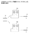
この例では上記の製造条件で作成した7種類の膜厚の硬化型保護部材12を以下の剥離条件でカード基板11に転写してIDカード100を作成した。このときの硬化型保護層12の膜厚と硬度との関係において、カード基板表面の耐擦過性及びバリの発生の有無を評価した。
剥離条件: 剥離角θ=30°
この際のIDカード100の耐擦過性に関しては、カード表面の硬化型保護層12をカナキン3号白布を用いて1kg/cm2 の荷重で1000回擦り、耐擦過性を評価した。バリに関しては、IDカード100の端部から凹凸状の転写箔残留片がはみ出しているか否かを目視評価によって行った。
【0157】
この結果、図28に示す表図が得られた。図28は硬化型保護部材12のバリの発生有無とカード基板の表面保護の両立性の評価例を示す表図である。図28において、二重マル印は「耐擦過性及びバリに関して全く問題なし」、丸印は「ほぼ問題なし」、三角印は「バリが発生するが支障はない」、及び、×印は「傷やバリが発生する」を示している。
【0158】
この実験結果によれば、硬化型保護層12の膜厚ThがTh<0.5μmときはバリが発生するが支障はない。しかしながら、Th<0.5μmときは硬度B〜4Hに関していずれも耐擦過性が劣化し、カード表面に傷が残ったり、剥離時に顔画像形成領域などにダメージを与える原因となる。
【0159】
また、膜厚ThがTh≧5.0μmときは硬度Bを除いて耐擦過性にはほぼ問題がないが、硬度HB〜4Hに関して例えば300μm以上のバリが発生し、バリ除去のための別途な工程を導入しなければならない。
【0160】
従って、硬化型保護層12の膜厚Thを0.5μm<Th<5.0μmに規定することにより、その保護部材形成時における加工性を悪化させることなく、しかも、カード基板上の表面保護性に優れ、かつ、耐擦過性(耐摩耗性)に優れたIDカード100を提供できることが明らかになった。
【0161】
▲5▼ 硬化型保護部材12の膜厚Thと転写温度Txとの関係評価
この例では上記の製造条件において、以下の5種の転写温度Txを変えて作成した硬度3Hの7種類の膜厚Thの硬化型保護部材12を上述の剥離条件でカード基板11に転写してIDカード100を作成した。このときの硬化型保護層12の膜厚と転写温度との関係において、カード基板表面の膜付き性及びバリの発生の有無を評価した。
【0162】
転写温度Tx: 90℃,100℃,190℃,230℃,250℃
この際のIDカード100の膜付き性に関しては、カード表面の硬化型保護層12をカッターナイフで2mm間隔に傷を付け、表面を粘着テープ(ニチバン#405)を接着させ、剥離角度180°で硬化型保護層12を素早く剥離を行いカード表面を目視評価した。バリの評価方法に関しては上述した通りである。
【0163】
この結果、図29に示す表図が得られた。図29は硬化型保護部材12の膜厚Thと転写温度Txとの関係評価例を示す表図である。図29において、二重マル印は「膜付き性及びバリに関して全く問題なし」、丸印は「ほぼ問題なし」、三角印は「バリが発生するが支障はない」、及び、×印は「剥離容易及びバリが発生する」を示している。
【0164】
この実験結果によれば、硬化型保護層12の膜厚ThがTh<0.5μmときはバリが発生するが支障はない。しかしながら、Th<0.5μmときは転写温度Tx関して90℃,100℃,190℃,230℃,250℃のいずれの場合も膜付き性が劣化し、カード表面から硬化型保護層12が容易に剥がれてしまったり、転写時に支持体が変形する原因となる。
【0165】
また、膜厚ThがTh≧5.0μmときは転写温度90℃及び250℃を除いて膜付き性はほぼ問題がないが、転写温度Tx関して90℃,100℃,190℃,230℃,250℃のいずれの場合も、例えば300μm以上のバリが発生し、バリ除去のための別途な工程を導入しなければならない。
【0166】
従って、硬化型保護層12の膜厚Thを0.5μm<Th<5.0μmに規定すると共に、転写温度Txを90℃<Tx<250℃に規定することにより、その保護部材形成時における加工性を悪化させることなく、しかも、カード基板上の表面保護性に優れ、かつ、高膜付き性に優れたIDカード100を提供できることが明らかになった。
【0167】
▲6▼ 硬化型保護部材12の膜厚Thと支持体16への接着力(剥離力)Fbとの関係評価
この例では上記の製造条件において接着層14の厚みを調整すると共に、硬化型保護部材12の膜厚Thと5つの接着力Fbとの関係を調整し、硬度3Hの7種類の膜厚の硬化型保護部材12を以下の剥離条件でカード基板11に転写してIDカード100を作成した。このときの硬化型保護層12の膜厚Thと接着力Fbとの関係において、カード基板端面のバリの発生の有無を評価した。
剥離条件: 剥離角θ=135°
接着力: 0.5g/cm,2.5g/cm,5.0g/cm,10g/cm
25g/cm
この際のIDカード100のバリの発生有無の評価方法に関しては上述した通りである。この結果、図30に示す表図が得られた。図30は硬化型保護部材12の膜厚Thと支持体16への接着力(剥離力)Fbとの関係評価例を示す表図である。図30において、二重マル印は「バリに関して全く問題なし」、丸印は「ほぼ問題なし」、三角印は「バリが発生するが支障はない」、×印は「バリが発生する」、及び、黒三角印は「転写不能」を示している。
【0168】
この実験結果によれば、硬化型保護層12の膜厚ThがTh=0.5μmときは、接着力Fb=0.5g/cm及び25g/cmを除いてほぼ「問題なし」である。しかしながら、膜厚ThがTh<0.5μmときは接着力Fb=0.5g/cm及び2.5g/cmでややバリが発生し、接着力Fb=5g/cm、10g/cm及び25g/cmで転写不良となる。
【0169】
また、膜厚ThがTh≧5.0μmときは、ほぼ接着力Fbが0.5g/cm,2.5g/cm,5.0g/cm,10g/cm,25g/cmのいずれの場合も、例えば300μm以上のバリが発生し、バリ除去のための別途な工程を導入しなければならない。
【0170】
従って、硬化型保護層12の膜厚Thを0.5μm<Th<5.0μmに規定すると共に、接着力Fbを0.5g/cm<Fb<25g/cmに規定することにより、その保護部材形成時における加工性を悪化させることなく、しかも、カード基板上の表面保護性に優れ、かつ、耐擦過性(耐摩耗性)に優れたIDカード100を提供できることが明らかになった。
【0173】
【発明の効果】
以上説明したように、本発明のIDカードの製造方法によれば、記録画像が形成された面のカード基板上にほぼ透明性の硬化型保護部材を転写することにより、膜厚が0.5μm乃至5.0μmに規定され、その接着力Fbが0.5g/ cm <Fb<25g/ cm に規定された硬化型保護層をカード基板上に形成するようになされる。
【0174】
この構成によって、カード基板上の表面保護性を低下させることなく、硬化型保護層のカード外端部でのバリの発生を無くすことができる。これにより、耐擦過性に優れたIDカードを歩留まり良くかつ再現性良く製造することができる。
【0177】
この発明は偽変造防止等が要求される接触式又は非接触式の電子カードや磁気カードに適用して極めて好適である。
【図面の簡単な説明】
【図1】実施形態としてのIDカード100の構造例を示す斜視図である。
【図2】顔画像入りカード101の積層構造例を示す断面図である。
【図3】A及びBは、他の顔画像入りカード102及び103の積層構造例を示す断面図である。
【図4】Aは、IDカード100の硬化型保護層12の平面及びBはその断面の構成例(その1)を示すイメージ図である。
【図5】Aは、IDカード100の硬化型保護層12の平面、及び、Bはその断面の構成例(その2)を示すイメージ図である。
【図6】他の顔画像入りカード104の硬化型保護層12の平面の構成例を示すイメージ図である。
【図7】実施形態としての熱転写シート200の積層構造例を示す断面図である。
【図8】熱転写シート200のハーフカット例を示す概念図である。
【図9】A〜Cは、実施形態としての熱転写シート200の形成例を示す工程図である。
【図10】Aは、ホットスタンプフィルム32の形成工程例を示す斜視図、Bは、ホログラム像形成時の構成例を示す一部断面図である。
【図11】Aは、ラミネートフィルム33の形成工程例(その1)を示す斜視図、Bは、ホログラム像形成時の構成例を示す一部断面図である。
【図12】ラミネートフィルム33の形成工程例(その2)を示す斜視図である。
【図13】A〜Cは、実施形態としてのIDカード100の形成工程例を示す断面図である。
【図14】カード基板11と熱転写シート200との位置合わせ例を示す概念図である。
【図15】実施形態としてのIDカードの製造装置300の構成例を示す概念図である。
【図16】実施形態としての転写用カートリッジ400の構成例を示す斜視図である。
【図17】ホットスタンプ装置500の構成例を示す概念図である。
【図18】他の転写用のカートリッジ401の構成例を示す断面図である。
【図19】A及びBは他の転写用のカートリッジ402の折曲げ機構50の構成例を示す断面図である。
【図20】A及びBは他の転写用カートリッジ403の折曲げ機構70の構成例を示す断面である。
【図21】A及びBは他の転写用カートリッジ404の折曲げ機構80の構成例を示す断面図である。
【図22】他の折曲げ機構90の構成例を示す概念図である。
【図23】A及びBは他の折曲げ機構90の動作例を示す概念図である。
【図24】2台のホットスタンプ装置50A及び50Bによる処理例(直列)を示す概念図である。
【図25】熱転写シート200の積層例を示す工程図である。
【図26】2台のホットスタンプ装置50A及び50Bによる処理例(並列)を示す概念図である。
【図27】各実施例に係る熱転写シート200の積層例を示す断面図である。
【図28】硬化型保護部材12の加工性とカード基板の表面保護の両立性の評価例を示す表図である。
【図29】硬化型保護部材12の膜厚Thと転写温度Txとの関係評価例を示す表図である。
【図30】硬化型保護部材12の膜厚Thと支持体16への接着力(剥離力)Fbとの関係評価例を示す表図である。
【符号の説明】
11 カード基板
12 硬化型保護層(硬化型保護部材)
13 ホログラム像
14 接着層(接着シート)
16 支持体
21 テープ収容部(筐体)
22 従動ローラ部(棒状体)
24 カード浮上防止板(突出部)
31 ベースフィルム
32 ホットスタンプフィルム
33 ラミネートフィルム
41,49 搬送ベルト装置
42 生カード供給部
43 画像形成部
46 画像チェック部
51 転写箔コア(部材供給部)
52 真空熱プレス装置
54 裁断装置
60 カード供給手段
100 IDカード
200 熱転写シート
300 IDカードの製造装置
301 画像形成装置(画像形成手段)
302 熱転写装置
400 熱転写シート用のカートリッジ(転写用カートリッジ)
500 ホットスタンプ装置[0001]
BACKGROUND OF THE INVENTION
The present invention is an ID card suitable for application to a card with a face image with an image protection layer that requires prevention of forgery and alteration.Made ofHow to makeTo the lawIt is related.
[0002]
[Prior art]
In recent years, in the service industry fields such as government offices, banks, companies, medical institutions and schools, identification documents, passports, alien registration cards, library use cards, cash cards, credit cards, licenses such as automobile licenses, employees, etc. ID cards such as personal identification cards, employee ID cards, membership cards, medical cards, and student ID cards are widely used. In this type of ID card, a face image for identity verification and character information images such as characters and symbols concerning the owner are recorded. For this reason, printing for the purpose of preventing falsification of ID cards is often performed.
[0003]
This face image is usually formed by a full-color image having multiple gradations, for example, by a sublimation thermal transfer recording method, a silver halide color photographic method, or the like. The character information image is composed of a binary image, and is formed by, for example, a melt type thermal transfer recording system, a sublimation type thermal transfer recording system, a silver halide color photographic system, an electrophotographic system, an ink jet system, or the like. Further, for the purpose of preventing forgery and alteration, holograms, fine patterns, etc. are employed. In addition, standard format printing is performed on the ID card as necessary.
[0004]
In order to protect these images, a protective layer is provided on the surface of the ID card as necessary. As a protective layer provided on the ID card, for example, as described in JP-A-6-222535, JP-A-6-222536, and JP-A-6-222537, an ultraviolet curable resin is applied to the card surface, and then ultraviolet rays are applied. A method of providing a protective layer by irradiating and curing, a method of providing a laminate protective layer as described in JP-A-2-139551, a heat-cured protective layer after applying an isocyanate compound on a photographic surface of silver halide And a method of transferring a curable transfer foil member and providing a transfer protective layer as disclosed in JP-A-8-224982.
[0005]
[Problems to be solved by the invention]
By the way, according to the conventional method of manufacturing an ID card using a curable transfer foil member, since this type of transfer foil member has a property of being cured by ultraviolet rays, the thicker the curable transfer foil member is, The surface protection on the card substrate is improved. On the other hand, it has been found that if the film thickness is too thick, the workability at the time of forming the transfer foil member deteriorates. For example, a so-called visible burr is generated at the end of the ID card. Thereafter, the protective layer that protrudes outward beyond the outer peripheral edge of the card board is referred to as an outer burr, and the inner burr is generated when the protective layer is not properly formed in the vicinity of the outer peripheral edge of the card board. .
[0006]
When this type of burr occurs, the following problems occur. When an external burr occurs, it takes time to remove the above-mentioned protruding protective layer, that is, a member residual piece, and when an internal burr and an external burr occur, both cause the protective layer to peel off. I found out that sometimes
[0007]
Further, it has been found that if the curable transfer foil member is thinned, the generation of burrs during formation of the transfer foil member can be suppressed, but the surface protection property is lowered. For example, if the recorded image after card completion is rubbed strongly, scratches will occur on the curable transfer foil member (hereinafter also referred to as curable protective member), and the scratches will remain on the recorded image. I found it.
[0008]
Accordingly, the present invention solves the above-described problems, and when a card substrate on which a face image or a character recording image is formed is protected by providing a curable protection member, the workability at the time of forming the protection member is improved. An ID car that can ensure surface protection on the card substrate without deterioratingMade ofHow to makeThe lawThe purpose is to provide.
[0010]
[Means for Solving the Problems]
In order to solve the above problems,The present inventors conducted an experiment to find an optimum film thickness value of the curable protective member with respect to the surface protective property on the card substrate and the workability when forming the protective member. According to this experimental result, when covering and protecting a transparent curable protective member on the card substrate on the recording image forming surface side, the film thickness of the curable protective member isTheSpecified to 0.5 μm to 5.0 μm, andAdhesive force Fb
0.5g / cm <Fb <25g / cm
Stipulated inIt is clear that it is possible to provide an ID card that does not deteriorate the workability at the time of forming the protective member, has excellent surface protection on the card substrate, and has excellent scratch resistance (wear resistance). Became.
[0011]
The method for producing an ID card of the present invention includes a step of forming a recorded image on a card substrate, and a curable protective layer formed by transferring a substantially transparent curable protective member onto the card substrate on the surface on which the recorded image is formed. And forming a process,The curable protective member is a transfer foil provided with an ultraviolet curable layer and an adhesive layer on a support, and when the curable protective layer is formed on the card substrate,BranchWhen the adhesive force between the holder and the UV curable layer is Fb,
0.5g / cm <Fb <25g / cm
Stipulated in
When the thickness of the curable protective layer is Th,
0.5 μm ≦ Th <5.0 μm
Stipulated inIt is characterized by this.
[0012]
According to the ID card manufacturing method of the present invention, the film thicknessTheSpecified to 0.5 μm to 5.0 μmAndThatAdhesive force Fb
0.5g / cm <Fb <25g / cm
Specified inSince the curable protective layer is formed on the card substrate, it is possible to eliminate the occurrence of burrs at the outer peripheral edge of the card of the curable protective layer without deteriorating the surface protection on the card substrate. Thereby, an ID card excellent in scratch resistance (wear resistance) can be manufactured with good reproducibility.
[0016]
DETAILED DESCRIPTION OF THE INVENTION
Hereinafter, an ID car as an embodiment of the present invention will be described with reference to the drawings.DeManufacturing methodTo the lawExplain about it.
[0017]
(1) ID card
FIG. 1 shows an embodiment of the present invention.Formed by manufacturing method2 is a perspective view showing a structural example of an
[0018]
In this embodiment, when a transparent curable protective member is provided on the card substrate on the surface on which the face image or the character recording image is formed, the film thickness, processing temperature, adhesive thickness of the member is protected. Providing an ID card that does not deteriorate the workability when forming a protective member, has excellent surface protection on the card substrate, and has excellent scratch resistance (wear resistance) It is something that can be done.
[0019]
The
[0020]
In this example, a recorded image such as a face image or a character recorded image is formed on the
[0021]
A transparent sheet-like curable protective layer (hereinafter also referred to as a curable protective member) 12 is provided on the
[0022]
In this example, a
[0023]
The
[0024]
FIG. 2 is a cross-sectional view showing an example of a laminated structure of the
0.5μm ≦ Th ≦ 5.0μm
Stipulated in Although it depends on the material of the curable
[0025]
The reason why the film thickness Th is defined is to achieve both the workability at the time of transfer of the curable
[0026]
The curable
[0027]
The curing time of the curable
[0028]
Further, the hardness of the curable
[0029]
Further, the
0.1 μm <t <20 μm
Stipulated in When the thickness t is defined in this way, it is possible to prevent the curable
[0030]
The
[0031]
In addition, Sumitomo Chemical's Sumic, Chisso Petrochemical's Bistack, Mitsubishi Yuka's Yucatak, Henkel's Macromelt Series, Mitsui Petrochemical's Toughmer, Ube Lexen's APAO, Eastman Polyolefin hot melt resins such as Eastman Bond manufactured by Chemical Company and A-FAX manufactured by Hercules are preferred. Furthermore, TE030 and TE100 manufactured by Sumitomo 3M Co., Ltd., Hibon 4820 manufactured by Hitachi Chemical Co., Ltd., and Kanebo NS Co., Ltd. are used. Hot melt resins such as Bond Master 170 series manufactured by Henkel and Macroplast QR3460 manufactured by Henkel are preferable, and hot melt resins based on ethylene / vinyl acetate copolymers and polyester hot melt resins are preferable. Hot melt resins have the property of absorbing moisture after curing and curing.
[0032]
The softening point of the
[0033]
3A and 3B are cross-sectional views showing examples of laminated structures of
[0034]
The
[0035]
In this example, when the film thickness of one curable
[0036]
At the same time, the surface protection after completion of the card is improved as compared with the other face image-containing
[0037]
As described above, it is possible to protect the face image and the character recording image formed on the card surface more firmly than when the single curable
[0038]
4A is a plan view of the curable
[0039]
In the
A + α⊇C⊃B (1)
It is made to have a relationship. Regarding this protrusion area α, when the protrusion distance of the curable
0 ≦ δ ≦ 300μm
Stipulated in In this manner, at least the image forming area B is protected by the curable
[0040]
As for the inner burr that protrudes from the outer peripheral edge of the card to the image forming region B side when the curable
0mm ≦ γ ≦ 0.8mm
Stipulated in If defined in this way, the image forming area B is protected by the curable
[0041]
In this example, a
[0042]
FIG. 6 is an image diagram showing a planar configuration example of the curable
[0043]
Depending on the use of the
[0044]
If defined in this way, the face image forming area P1, the personal information writing area P2, and the standard format area P3 are protected by the curable
[0045]
(2) Thermal transfer sheet
FIG. 7 is a cross-sectional view illustrating a laminated structure example of the
[0046]
A
0.5μm ≦ Th ≦ 5.0μm
Stipulated in A
0.1 μm <t <20 μm
Stipulated in The reason for these regulations is as described above.
[0047]
FIG. 8 is a conceptual diagram showing a half cut example of the
[0048]
This incision is sharply formed using a cutter or the like that replicates the shape of the card substrate, and is smaller than the
[0049]
As described above, according to the
[0050]
(3) Manufacturing method of thermal transfer sheet
9A to 9C are process diagrams showing an example of forming the
[0051]
First, in FIG. 9A, a curable
[0052]
Thereafter, in FIG. 9B, the
[0053]
In addition to holograms, printing for the purpose of preventing falsification includes a composition containing at least one selected from a fine pattern, a watermark, and {reflective beads, ultraviolet absorbers, infrared absorbers, fluorescent brighteners}. Examples of known methods for printing layers, magnetic recording layers, and barcodes formed from materials may be mentioned, but these may be used alone or in combination of two or more thereof. For example, a method using reflective beads is described in JP-A-6-507737.
[0054]
Thereafter, in FIG. 9C, an adhesive member is applied on the
[0055]
As described above, according to the method for producing a thermal transfer sheet of the present invention, the curable
[0056]
FIG. 10A is a perspective view illustrating an example of a process for forming a
[0057]
Also in this case, the relational expression of A + α · C · B shown in the above equation (1) and the outer periphery of the
[0058]
In this example,
[0059]
For example, when forming the
[0060]
At this time, positioning pins 38A and 38B are inserted from the hologram image creating means 34 into the opening
[0061]
FIG. 11A is a perspective view illustrating an example (part 1) of forming a
[0062]
Of course, the surface on which the
[0063]
At the time of bonding of the
[0064]
When these
[0065]
(4) ID card manufacturing method
FIG. 13A to FIG. 13C are cross-sectional views showing an example of forming the
[0066]
In this embodiment, a recorded image is formed on the
[0067]
Based on these assumptions, in FIG. 13A, the curable
0g <Fc <20kg
Stipulated in When Fc> 20 kg, the curable
90 ° C <Tx <250 ° C
Stipulated in
[0068]
The transfer temperature Tx is defined in this way because when Tx <90 ° C. and Tx> 250 ° C., the peelability of the curable
[0069]
In this example, the
[0070]
Thereafter, in FIG. 13B, the
200g <Fa <1.5kg
Stipulated in Although it depends on the material of the curable
[0071]
The tension Fa is defined in this way because, when Fa <200 g and Fa> 1.5 kg, the peelability of the curable
V1 <V2
Stipulated in
[0072]
For example, the moving speed V2 of the
1.02 ・ V1 <V2 <1.4 ・ V1
Stipulated in That is, the speed difference Vε between the moving speed V1 of the
[0073]
In this example, when the
[0074]
Thereafter, in FIG. 13C, the curable
0.5g / cm <Fb <25g / cm
Stipulated in Although depending on the material of the curable
[0075]
The adhesive force Fb is defined in this way because when Fb <0.5 g / cm and Fb> 25 g / cm, the peeling of the curable
[0076]
In this example, when the
10 ° <θ <150 °
Stipulated in Although it depends on the material of the curable
[0077]
The peel angle θ is defined in this way because when θ <10 ° and θ> 150 °, the peelability of the curable
[0078]
By defining the peel angle θ as 10 ° <θ <150 °, the curable
[0079]
Note that the curable
[0080]
Further, when transferring the curable
[0081]
Furthermore, the curable
[0082]
Thus, according to the method of manufacturing the
[0083]
Moreover, according to this embodiment, the curable
[0084]
(5) ID card manufacturing equipment
FIG. 15 shows an embodiment.Manufacturing method is appliedIt is a conceptual diagram which shows the structural example of the
[0085]
The ID
[0086]
An ID
[0087]
A sign panel or a writing layer for a driver's license may be provided on the back surface of the
[0088]
The
[0089]
In the image forming apparatus 301, when the
[0090]
Further, an image check unit 46 is provided on the downstream side of the information writing unit 44 with the first drive roller 45 interposed therebetween, and a user's face photograph formed by the image forming unit 43, a name, a card issuance date, and the like. It is checked for mistakes. When the information writing unit 44 described above is provided, an information check unit 48 is further provided on the downstream side of the image check unit 46 with the
[0091]
The image forming apparatus 301 is combined with a thermal transfer device (transfer means) 302, and the transparent curable
[0092]
In this example, a
[0093]
Further, the
[0094]
The
[0095]
The vacuum heat press device 52 has a flat press portion disposed on the conveyance path, and a predetermined pressure is applied from above the
[0096]
In this example, although depending on the kind of the
[0097]
Moreover, the cooling part 53 is provided in the downstream of the vacuum hot press apparatus 52, and the
[0098]
Next, the operation of the ID
[0099]
Thereafter, the
[0100]
When the
[0101]
In the vacuum heat press device 52, the
[0102]
A mechanism for bending the rear end in a direction away from the curable
[0103]
As described above, according to the ID
[0104]
Therefore, since the curable
[0105]
(6) Cartridge for thermal transfer sheet
FIG. 16 is a perspective view illustrating a configuration example of a
[0106]
The
[0107]
Also in this example, the
[0108]
The rotational power of the
[0109]
This driven
[0110]
The peeling rod-like body is not limited to the driven
[0111]
Furthermore, in this example, a card floating
[0112]
FIG. 17 is a conceptual diagram illustrating a configuration example of a
[0113]
A
[0114]
For example, the
[0115]
Therefore, when the
[0116]
When the
[0117]
Also during the heating, when the driven
[0118]
Thus, according to the
[0119]
Accordingly, since only the
[0120]
FIG. 18 is a cross-sectional view showing a configuration example of another
[0121]
The card end floating prevention mechanism (contact means) 60 shown in FIG. 18 includes a driven
[0122]
In this example, when the peeling angle θ is an angle at which the thermal transfer sheet (support 16) 200 is pulled from the
10 ° <θ <150 °
Stipulated in The peel angle θ is defined in this way because when θ <10 ° and θ> 150 °, the peelability of the curable
[0123]
In this example, a driven
[0124]
For example, after the adjustment of the peel angle θ, the member holding portion 63 is fixed to the
[0125]
FIGS. 19A and 19B are cross-sectional views showing a configuration example of a
[0126]
The
[0127]
In this example, when the
[0128]
20A and 20B are cross-sectional views showing a configuration example of the
[0129]
A
[0130]
In this example, when the
[0131]
FIGS. 21A and 21B are cross-sectional views showing a configuration example of a
[0132]
The
[0133]
In this example, when the
[0134]
FIG. 22 is a conceptual diagram illustrating a configuration example of another
[0135]
A
[0136]
A
[0137]
A
[0138]
In addition, a dump drive unit 95 is provided at the lower right end of the
[0139]
Subsequently, an operation example of the bending mechanism of the
[0140]
On the premise of this, when the
[0141]
Based on the drive control signal S2, the
[0142]
In addition, a
[0143]
Next, a case where a transfer process is performed using a plurality of
[0144]
In this example, two
[0145]
When serial processing is performed in this way, after the first curable
[0146]
Thereby, generation | occurrence | production of a burr | flash is further suppressed by transferring the hardening
[0147]
FIG. 26 is a conceptual diagram showing another processing example (parallel) by the two
[0148]
The
[0149]
This allows you to obtain identification cards, passports, alien registration cards, library cards, cash cards, credit cards, licenses such as automobile licenses, employee ID cards, employee ID cards, membership cards, medical cards and student ID cards. Ideal for processing large quantities at once.
[0150]
(7) Examples
The present inventors find out the optimum film thickness Th, hardness, transfer temperature Tx, and adhesive force (peeling force) Fb of the curable
[0151]
(1) Preparation example of
FIG. 27 is a cross-sectional view showing a structural example of the
[0152]
In this example, on the 25 μm polyethylene terephthalate film as the
[0153]
Next, the following compositions as an intermediate layer 19 and a primer layer 20 were sequentially applied onto the curable
Intermediate layer Dry film thickness 0.5μm
70 parts polyvinyl butyral
Isocyanate 30 parts
700 parts of methyl ethyl ketone
Primer layer Dry film thickness 0.5μm
Polyvinyl butyral 50 parts
350 parts of methyl ethyl ketone
350 parts of toluene
Thereafter, the following adhesive member was applied on the primer layer 20 with a wire bar and dried to form the
Adhesive layer Dry film thickness 1μm
100 parts urethane modified olefin resin (manufactured by Toho Chemical Industry: Hitech S8529)
Thereby, the
[0154]
(2) Example of creating a card substrate having a face image and a character recording image
A white polypropylene layer made of 50 μm white polypropylene (manufactured by Mitsubishi Oil Chemical Co., Ltd .: Naprene FL25HA) is thermally attached to both sides of 350 μm polyethylene terephthalate as the support 11C shown in FIG. 2 and 450 μm composite support.
Colloidal silica 2.5 parts
7.2 parts of gelatin
Dichlorotriazine curing agent 0.3 parts
100 parts of water
Further, a heat sublimation type
[0155]
(3) Example of making
The heat heat roller 27 (transfer temperature of 190 ° C., transfer speed of 5 cm / second) is made so that the surface side of the
[0156]
(4) Evaluation of compatibility between processability of curable
In this example, the
Peeling condition: Peeling angle θ = 30 °
Regarding the scratch resistance of the
[0157]
As a result, the table shown in FIG. 28 was obtained. FIG. 28 is a table showing an evaluation example of the compatibility between the occurrence of burrs in the curable
[0158]
According to the experimental result, when the film thickness Th of the curable
[0159]
In addition, when the film thickness Th is Th ≧ 5.0 μm, there is almost no problem with the scratch resistance except for the hardness B, but for the hardness HB to 4H, burrs of, for example, 300 μm or more are generated. A process must be introduced.
[0160]
Therefore, by defining the film thickness Th of the curable
[0161]
(5) Evaluation of relationship between film thickness Th of curable
In this example, under the manufacturing conditions described above, the curable
[0162]
Transfer temperature Tx: 90 ° C, 100 ° C, 190 ° C, 230 ° C, 250 ° C
In this case, the
[0163]
As a result, the table shown in FIG. 29 was obtained. FIG. 29 is a table showing a relationship evaluation example between the film thickness Th of the curable
[0164]
According to the experimental result, when the film thickness Th of the curable
[0165]
Further, when the film thickness Th is Th ≧ 5.0 μm, there is almost no problem with the film adhesion except for the transfer temperatures of 90 ° C. and 250 ° C. However, the transfer temperature Tx is 90 ° C., 100 ° C., 190 ° C., 230 ° C., In any case of 250 ° C., for example, burrs of 300 μm or more are generated, and a separate process for removing burrs must be introduced.
[0166]
Therefore, the thickness Th of the curable
[0167]
(6) Evaluation of relationship between film thickness Th of curable
In this example, the thickness of the
Peeling condition: Peeling angle θ = 135 °
Adhesive strength: 0.5 g / cm, 2.5 g / cm, 5.0 g / cm, 10 g / cm
25g / cm
The evaluation method for the presence or absence of burrs on the
[0168]
According to this experimental result, when the film thickness Th of the curable
[0169]
When the film thickness Th is Th ≧ 5.0 μm, the adhesive force Fb is almost 0.5 g / cm, 2.5 g / cm, 5.0 g / cm, 10 g / cm, or 25 g / cm. For example, burrs of 300 μm or more are generated, and a separate process for removing burrs must be introduced.
[0170]
Therefore, by defining the thickness Th of the curable
[0173]
【The invention's effect】
As explained above,According to the ID card manufacturing method of the present invention, the film thickness is regulated to 0.5 μm to 5.0 μm by transferring a substantially transparent curable protective member onto the card substrate on the surface on which the recorded image is formed. IsThe adhesive force Fb is 0.5 g / cm <Fb <25g / cm Stipulated inTo form a curable protective layer on the card substrateDone.
[0174]
With this configuration, it is possible to eliminate the occurrence of burrs at the card outer end of the curable protective layer without deteriorating the surface protection on the card substrate. Thereby, an ID card excellent in scratch resistance can be manufactured with good yield and good reproducibility.
[0177]
The present invention is extremely suitable when applied to contact-type or non-contact-type electronic cards and magnetic cards that require prevention of forgery and alteration.
[Brief description of the drawings]
FIG. 1 is a perspective view showing a structural example of an
FIG. 2 is a cross-sectional view showing an example of a laminated structure of a
FIGS. 3A and 3B are cross-sectional views showing an example of a laminated structure of
4A is an image view showing a configuration example (No. 1) of a cross section of the plane of the curable
FIG. 5A is a plan view of the curable
FIG. 6 is an image diagram showing a configuration example of a plane of the curable
FIG. 7 is a cross-sectional view showing an example of a laminated structure of a
FIG. 8 is a conceptual diagram illustrating a half cut example of a
9A to 9C are process diagrams showing an example of forming a
FIG. 10A is a perspective view showing an example of a process for forming a
FIG. 11A is a perspective view illustrating an example of a process for forming a laminate film 33 (part 1), and FIG. 11B is a partial cross-sectional view illustrating an example of a configuration when forming a hologram image.
12 is a perspective view showing an example (part 2) of forming a
FIGS. 13A to 13C are cross-sectional views illustrating an example of a process for forming an
14 is a conceptual diagram showing an example of alignment between the
FIG. 15 is a conceptual diagram showing a configuration example of an ID
FIG. 16 is a perspective view showing a configuration example of a
FIG. 17 is a conceptual diagram showing a configuration example of a
18 is a cross-sectional view showing a configuration example of another
FIGS. 19A and 19B are cross-sectional views illustrating a configuration example of a
FIGS. 20A and 20B are cross sections showing a configuration example of a
FIGS. 21A and 21B are cross-sectional views showing a configuration example of a
22 is a conceptual diagram showing a configuration example of another
FIGS. 23A and 23B are conceptual diagrams showing an operation example of another
FIG. 24 is a conceptual diagram showing a processing example (in series) performed by two
FIG. 25 is a process diagram illustrating an example of stacking of
FIG. 26 is a conceptual diagram showing a processing example (parallel) by two
FIG. 27 is a cross-sectional view showing a lamination example of a
FIG. 28 is a table showing an evaluation example of compatibility between workability of the curable
FIG. 29 is a table showing a relationship evaluation example between the film thickness Th of the curable
30 is a table showing an example of evaluating the relationship between the film thickness Th of the curable
[Explanation of symbols]
11 Card board
12 Curable protective layer (Curable protective member)
13 Hologram image
14 Adhesive layer (adhesive sheet)
16 Support
21 Tape housing (housing)
22 Driven roller (rod-like body)
24 Card levitation prevention plate (protrusion)
31 Base film
32 Hot stamp film
33 Laminate film
41, 49 Conveyor belt device
42 Raw card supply department
43 Image forming unit
46 Image check section
51 Transfer foil core (component supply unit)
52 Vacuum heat press equipment
54 Cutting device
60 Card supply means
100 ID card
200 Thermal transfer sheet
300 ID card manufacturing equipment
301 Image forming apparatus (image forming means)
302 Thermal transfer device
400 Thermal transfer sheet cartridge (transfer cartridge)
500 hot stamping equipment
Claims (5)
前記記録画像が形成された面のカード基板上にほぼ透明性の硬化型保護部材を転写して硬化型保護層を形成する工程とを有し、
前記硬化型保護部材は、
支持体に紫外線硬化層及び接着層を設けた転写箔であり、
前記硬化型保護層をカード基板上に形成する際に、
前記支持体と紫外線硬化層の接着力をFbとしたとき、
0.5g/ cm <Fb<25g/ cm
に規定され、
前記硬化型保護層の膜厚をThとしたとき、
0.5μm≦Th<5.0μm
に規定されることを特徴とするIDカードの製造方法。Forming a recorded image on the card substrate;
Forming a curable protective layer by transferring a substantially transparent curable protective member onto the card substrate on the surface on which the recorded image is formed,
The curable protective member is
It is a transfer foil provided with an ultraviolet curable layer and an adhesive layer on a support,
When forming the curable protective layer on the card substrate,
When the adhesive strength of the supporting lifting member and the UV cured layer was set to Fb,
0.5 g / cm <Fb <25 g / cm
Stipulated in
When the thickness of the curable protective layer is Th,
0.5 μm ≦ Th < 5.0 μm
Defined ID card manufacturing method characterized by and Turkey on.
0.1μm<t<20μm
に規定されることを特徴とする請求項1に記載のIDカードの製造方法。When the thickness of the adhesive layer is t,
0.1 μm <t <20 μm
The method of manufacturing an ID card according to claim 1 , wherein
90℃<Tx<250℃
に規定されることを特徴とする請求項1乃至3に記載のいずれかのIDカードの製造方法。When the processing temperature when transferring the curable protective member onto the card substrate is Tx,
90 ° C <Tx <250 ° C
The method of manufacturing an ID card according to claim 1, wherein the ID card is defined as follows.
Priority Applications (1)
| Application Number | Priority Date | Filing Date | Title |
|---|---|---|---|
| JP2000120046A JP3879363B2 (en) | 1999-04-23 | 2000-04-20 | ID card manufacturing method |
Applications Claiming Priority (3)
| Application Number | Priority Date | Filing Date | Title |
|---|---|---|---|
| JP11-117361 | 1999-04-23 | ||
| JP11736199 | 1999-04-23 | ||
| JP2000120046A JP3879363B2 (en) | 1999-04-23 | 2000-04-20 | ID card manufacturing method |
Publications (3)
| Publication Number | Publication Date |
|---|---|
| JP2001001673A JP2001001673A (en) | 2001-01-09 |
| JP2001001673A5 JP2001001673A5 (en) | 2005-04-07 |
| JP3879363B2 true JP3879363B2 (en) | 2007-02-14 |
Family
ID=26455492
Family Applications (1)
| Application Number | Title | Priority Date | Filing Date |
|---|---|---|---|
| JP2000120046A Expired - Fee Related JP3879363B2 (en) | 1999-04-23 | 2000-04-20 | ID card manufacturing method |
Country Status (1)
| Country | Link |
|---|---|
| JP (1) | JP3879363B2 (en) |
Families Citing this family (2)
| Publication number | Priority date | Publication date | Assignee | Title |
|---|---|---|---|---|
| JP2005530198A (en) * | 2002-06-13 | 2005-10-06 | スリーエム イノベイティブ プロパティズ カンパニー | Managed certificate manufacturing and management system |
| WO2004096898A1 (en) * | 2003-04-28 | 2004-11-11 | Konica Minolta Photo Imaging, Inc. | Transfer foil supporting body, transfer foil, and id card manufacturing method |
-
2000
- 2000-04-20 JP JP2000120046A patent/JP3879363B2/en not_active Expired - Fee Related
Also Published As
| Publication number | Publication date |
|---|---|
| JP2001001673A (en) | 2001-01-09 |
Similar Documents
| Publication | Publication Date | Title |
|---|---|---|
| JP5111650B2 (en) | Identification card printer for assembling store card-assembling device | |
| US5890742A (en) | Identification document and personalization and assembly process | |
| US7824029B2 (en) | Identification card printer-assembler for over the counter card issuing | |
| JP5304018B2 (en) | Method for manufacturing patch intermediate transfer recording medium | |
| US7762590B2 (en) | Individualized security document | |
| US20050189066A1 (en) | Laminated cards and methods of manufacture for secure applications | |
| JPH08224982A (en) | Transfer foil and id card using the same | |
| WO1999044837A1 (en) | Intermediate transfer recording medium, method of forming print, and print | |
| WO1990005640A1 (en) | Imaging plastics articles | |
| JP3879362B2 (en) | ID card manufacturing method and manufacturing apparatus thereof | |
| US10105981B2 (en) | Transfer lamination | |
| JP2007226736A (en) | Ic card and ic card manufacturing method | |
| JPH1178266A (en) | Thermal destruction transfer foil and thermal recording medium | |
| JP3879363B2 (en) | ID card manufacturing method | |
| JP2001001674A (en) | Id card, method and apparatus for manufacturing it, thermal transfer sheet and its manufacture | |
| JPH0740690A (en) | Id card and its preparation | |
| JP2001001619A (en) | Cartridge for thermal transfer sheet | |
| JPH11254844A (en) | Intermediate transfer recording medium, method for forming printed matter using the same and printed matter formed by method | |
| EP2081768A2 (en) | Mini patch laminate | |
| JP3371683B2 (en) | Image forming method and image forming apparatus, and transfer medium used therein | |
| JP2013116580A (en) | Transfer device | |
| JP2006178566A (en) | Ic card manufacturing method, ic card manufacturing apparatus and ic card | |
| JP2007047937A (en) | Ic card and manufacturing method of ic card | |
| JP2009274291A (en) | Patch intermediate transfer recording medium and forgery prevention medium using the same | |
| JP2007058667A (en) | Ic card |
Legal Events
| Date | Code | Title | Description |
|---|---|---|---|
| A521 | Written amendment |
Free format text: JAPANESE INTERMEDIATE CODE: A523 Effective date: 20040512 |
|
| A621 | Written request for application examination |
Free format text: JAPANESE INTERMEDIATE CODE: A621 Effective date: 20040512 |
|
| A977 | Report on retrieval |
Free format text: JAPANESE INTERMEDIATE CODE: A971007 Effective date: 20060515 |
|
| RD04 | Notification of resignation of power of attorney |
Free format text: JAPANESE INTERMEDIATE CODE: A7424 Effective date: 20060515 |
|
| A131 | Notification of reasons for refusal |
Free format text: JAPANESE INTERMEDIATE CODE: A131 Effective date: 20060523 |
|
| A521 | Written amendment |
Free format text: JAPANESE INTERMEDIATE CODE: A523 Effective date: 20060724 |
|
| TRDD | Decision of grant or rejection written | ||
| A01 | Written decision to grant a patent or to grant a registration (utility model) |
Free format text: JAPANESE INTERMEDIATE CODE: A01 Effective date: 20061017 |
|
| A61 | First payment of annual fees (during grant procedure) |
Free format text: JAPANESE INTERMEDIATE CODE: A61 Effective date: 20061030 |
|
| R150 | Certificate of patent or registration of utility model |
Ref document number: 3879363 Country of ref document: JP Free format text: JAPANESE INTERMEDIATE CODE: R150 Free format text: JAPANESE INTERMEDIATE CODE: R150 |
|
| FPAY | Renewal fee payment (event date is renewal date of database) |
Free format text: PAYMENT UNTIL: 20091117 Year of fee payment: 3 |
|
| S111 | Request for change of ownership or part of ownership |
Free format text: JAPANESE INTERMEDIATE CODE: R313113 |
|
| FPAY | Renewal fee payment (event date is renewal date of database) |
Free format text: PAYMENT UNTIL: 20091117 Year of fee payment: 3 |
|
| R350 | Written notification of registration of transfer |
Free format text: JAPANESE INTERMEDIATE CODE: R350 |
|
| S111 | Request for change of ownership or part of ownership |
Free format text: JAPANESE INTERMEDIATE CODE: R313114 |
|
| FPAY | Renewal fee payment (event date is renewal date of database) |
Free format text: PAYMENT UNTIL: 20091117 Year of fee payment: 3 |
|
| R350 | Written notification of registration of transfer |
Free format text: JAPANESE INTERMEDIATE CODE: R350 |
|
| FPAY | Renewal fee payment (event date is renewal date of database) |
Free format text: PAYMENT UNTIL: 20091117 Year of fee payment: 3 |
|
| FPAY | Renewal fee payment (event date is renewal date of database) |
Free format text: PAYMENT UNTIL: 20101117 Year of fee payment: 4 |
|
| R250 | Receipt of annual fees |
Free format text: JAPANESE INTERMEDIATE CODE: R250 |
|
| FPAY | Renewal fee payment (event date is renewal date of database) |
Free format text: PAYMENT UNTIL: 20111117 Year of fee payment: 5 |
|
| R250 | Receipt of annual fees |
Free format text: JAPANESE INTERMEDIATE CODE: R250 |
|
| FPAY | Renewal fee payment (event date is renewal date of database) |
Free format text: PAYMENT UNTIL: 20111117 Year of fee payment: 5 |
|
| FPAY | Renewal fee payment (event date is renewal date of database) |
Free format text: PAYMENT UNTIL: 20121117 Year of fee payment: 6 |
|
| R250 | Receipt of annual fees |
Free format text: JAPANESE INTERMEDIATE CODE: R250 |
|
| FPAY | Renewal fee payment (event date is renewal date of database) |
Free format text: PAYMENT UNTIL: 20131117 Year of fee payment: 7 |
|
| R250 | Receipt of annual fees |
Free format text: JAPANESE INTERMEDIATE CODE: R250 |
|
| R250 | Receipt of annual fees |
Free format text: JAPANESE INTERMEDIATE CODE: R250 |
|
| R250 | Receipt of annual fees |
Free format text: JAPANESE INTERMEDIATE CODE: R250 |
|
| R250 | Receipt of annual fees |
Free format text: JAPANESE INTERMEDIATE CODE: R250 |
|
| R250 | Receipt of annual fees |
Free format text: JAPANESE INTERMEDIATE CODE: R250 |
|
| R250 | Receipt of annual fees |
Free format text: JAPANESE INTERMEDIATE CODE: R250 |
|
| R250 | Receipt of annual fees |
Free format text: JAPANESE INTERMEDIATE CODE: R250 |
|
| LAPS | Cancellation because of no payment of annual fees |