JP3804349B2 - Thin film device device manufacturing method, active matrix substrate manufacturing method, and electro-optical device - Google Patents
Thin film device device manufacturing method, active matrix substrate manufacturing method, and electro-optical device Download PDFInfo
- Publication number
- JP3804349B2 JP3804349B2 JP22433299A JP22433299A JP3804349B2 JP 3804349 B2 JP3804349 B2 JP 3804349B2 JP 22433299 A JP22433299 A JP 22433299A JP 22433299 A JP22433299 A JP 22433299A JP 3804349 B2 JP3804349 B2 JP 3804349B2
- Authority
- JP
- Japan
- Prior art keywords
- thin film
- substrate
- film device
- layer
- base material
- Prior art date
- Legal status (The legal status is an assumption and is not a legal conclusion. Google has not performed a legal analysis and makes no representation as to the accuracy of the status listed.)
- Expired - Fee Related
Links
Images


Classifications
-
- H—ELECTRICITY
- H01—ELECTRIC ELEMENTS
- H01L—SEMICONDUCTOR DEVICES NOT COVERED BY CLASS H10
- H01L2221/00—Processes or apparatus adapted for the manufacture or treatment of semiconductor or solid state devices or of parts thereof covered by H01L21/00
- H01L2221/67—Apparatus for handling semiconductor or electric solid state devices during manufacture or treatment thereof; Apparatus for handling wafers during manufacture or treatment of semiconductor or electric solid state devices or components; Apparatus not specifically provided for elsewhere
- H01L2221/683—Apparatus for handling semiconductor or electric solid state devices during manufacture or treatment thereof; Apparatus for handling wafers during manufacture or treatment of semiconductor or electric solid state devices or components; Apparatus not specifically provided for elsewhere for supporting or gripping
- H01L2221/68304—Apparatus for handling semiconductor or electric solid state devices during manufacture or treatment thereof; Apparatus for handling wafers during manufacture or treatment of semiconductor or electric solid state devices or components; Apparatus not specifically provided for elsewhere for supporting or gripping using temporarily an auxiliary support
- H01L2221/68363—Apparatus for handling semiconductor or electric solid state devices during manufacture or treatment thereof; Apparatus for handling wafers during manufacture or treatment of semiconductor or electric solid state devices or components; Apparatus not specifically provided for elsewhere for supporting or gripping using temporarily an auxiliary support used in a transfer process involving transfer directly from an origin substrate to a target substrate without use of an intermediate handle substrate
-
- H—ELECTRICITY
- H01—ELECTRIC ELEMENTS
- H01L—SEMICONDUCTOR DEVICES NOT COVERED BY CLASS H10
- H01L2221/00—Processes or apparatus adapted for the manufacture or treatment of semiconductor or solid state devices or of parts thereof covered by H01L21/00
- H01L2221/67—Apparatus for handling semiconductor or electric solid state devices during manufacture or treatment thereof; Apparatus for handling wafers during manufacture or treatment of semiconductor or electric solid state devices or components; Apparatus not specifically provided for elsewhere
- H01L2221/683—Apparatus for handling semiconductor or electric solid state devices during manufacture or treatment thereof; Apparatus for handling wafers during manufacture or treatment of semiconductor or electric solid state devices or components; Apparatus not specifically provided for elsewhere for supporting or gripping
- H01L2221/68304—Apparatus for handling semiconductor or electric solid state devices during manufacture or treatment thereof; Apparatus for handling wafers during manufacture or treatment of semiconductor or electric solid state devices or components; Apparatus not specifically provided for elsewhere for supporting or gripping using temporarily an auxiliary support
- H01L2221/68368—Apparatus for handling semiconductor or electric solid state devices during manufacture or treatment thereof; Apparatus for handling wafers during manufacture or treatment of semiconductor or electric solid state devices or components; Apparatus not specifically provided for elsewhere for supporting or gripping using temporarily an auxiliary support used in a transfer process involving at least two transfer steps, i.e. including an intermediate handle substrate
Landscapes
- Liquid Crystal (AREA)
- Thin Film Transistor (AREA)
- Devices For Indicating Variable Information By Combining Individual Elements (AREA)
Description
【0001】
【発明の属する技術分野】
本発明は、薄膜デバイス装置の製造方法、この薄膜デバイス装置の製造方法を利用したアクティブマトリクス基板の製造方法、およびこのアクティブマトリクス基板を用いた電気光学装置に関するものである。さらに詳しくは、薄膜デバイスを基板上に形成した後、この基板から他の基板に薄膜デバイスを転写する技術に関するものである。
【0002】
【従来の技術】
各種の電気光学装置のうち、電気光学物質として液晶を用いたアクティブマトリクス型の液晶表示装置では、アクティブマトリクス基板上にスイッチング素子として薄膜トランジスタ(以下、TFTという。)を製造する際に、半導体プロセスを利用する。このプロセス中は高温処理を伴う工程を含むため、基板としては耐熱性に優れる材質のもの、すなわち、軟化点および融点が高いものを使用する必要がある。従って、現在は、1000℃程度の温度に耐える基板として石英ガラスが使用され、500℃前後の温度に耐える基板として耐熱ガラスが使用されている。
【0003】
このように、TFT等の薄膜デバイスを搭載する基板は、それらの薄膜デバイスを製造する際の温度条件等に耐え得るものでなければならない。
【0004】
しかしながら、TFT等の薄膜デバイスを搭載した基板が完成した後において、前記の石英ガラスや耐熱ガラスでは好ましくないことがある。例えば、高温処理を伴う製造プロセスに耐え得るように石英基板や耐熱ガラス基板等を用いた場合には、これらの基板が非常に高価であるため、表示装置等の製品価格の上昇を招く。また、パームトップコンピュータや携帯電話機等の携帯用電子機器に使用される液晶表示装置は、可能な限り安価であることに加えて、軽くて多少の変形にも耐え得ること、落としても割れにくいことも求められるが、石英基板やガラス基板は、重いとともに、変形に弱く、かつ、落下等によって割れやすい。従って、従来の薄膜デバイス装置に用いられる基板は、製造条件からくる制約、および製品に要求される特性の双方に対応することができないという問題点がある。
【0005】
そこで、本願出願人は、従来のプロセスと略同様な条件で薄膜デバイスを第1の基材上に形成した後に、この薄膜デバイスを第1の基材から剥離して、第2の基材に転写する技術を提案している(特願平8−225643号)。ここに提案した技術では、第1の基材と薄膜デバイスとの間に分離層を形成し、この分離層に対して例えばエネルギー光を照射することにより、第1の基材から薄膜デバイスを剥離して、この薄膜デバイスを第2の基材の側に転写する。
【0006】
【発明が解決しようとする課題】
しかしながら、従来の剥離方法および転写方法では、第1基板から薄膜デバイスを剥離させる際に、エネルギー光を分離層に照射しただけでは、分離層での剥離現象が適正に起こらないという問題点がある。例えば、第1の基材に対して、分離層として、水素ガスを含有するアモルファスシリコン膜を形成した後、このアモルファスシリコン膜にレーザ光を照射して剥離現象を生じさせることにより薄膜デバイスの側から第1の基材を剥がす際に、アモルファスシリコン膜から水素ガスが急激に発生して薄膜デバイスが損傷するという問題点がある。
【0007】
以上の問題点に鑑みて、本発明は、分離層として用いた水素含有のアモルファスシリコン膜に対するエネルギー光の照射条件を適正化することにより、薄膜デバイスを損傷することなく基板から剥離して、他の基板に転写することのできる薄膜デバイス装置の製造方法、この製造方法により得た薄膜デバイス装置、この薄膜デバイス装置の製造方法を用いたアクティブマトリクス基板の製造方法、この製造方法により製造したアクティブマトリクス基板、およびこのアクティブマトリクス基板を用いた電気光学装置を提供することにある。
【0008】
【課題を解決するための手段】
上記課題を解決するために、本発明は、第1の基材上にアモルファスシリコン膜を形成する第1の工程と、前記アモルファスシリコン膜に水素を導入することにより第1の分離層を形成する第2の工程と、前記第1の分離層上に薄膜デバイスを形成する第3の工程と、前記薄膜デバイスの前記第1の基材と反対側に第2の基材を接着する第4の工程と、前記第1の分離層の層内または前記第1の分離層の界面のうちの少なくとも一方で剥離現象を生じさせて、前記薄膜デバイスを前記第2の基材側に転写する第5の工程と、を具備し、前記第5の工程では、前記第1の分離層にエネルギー光を照射させることによってガスを発生させるとともに、前記エネルギー光のエネルギー密度を低密度から高密度に変化させることを特徴とする。
また、本発明は、上記に記載の発明であって、前記第5の工程では、前記エネルギー光としてレーザ光を照射することを特徴とする。
また、本発明は、上記に記載の発明であって、前記第5の工程では、前記エネルギー光のエネルギー密度を連続的に変化させてもよいし、段階的に変化させてもよい。
また、本発明は、上記に記載の発明であって、前記第4の工程では、前記薄膜デバイスの前記第1の基材と反対側に前記第2の基材を第2の分離層を介して接着し、前記第5の工程で前記第2の基材に前記薄膜デバイスを転写した後、前記薄膜デバイスの前記第2の基材と反対側に第3の基材を接着する第6の工程と、前記第2の分離層の層内または前記第2の分離層の界面のうちの少なくとも一方で剥離現象を生じさせることにより前記第2の基材を前記薄膜デバイス側から剥がして前記薄膜デバイスを前記第3の基材側に転写する第7の工程と、を有することを特徴とする。
また、本発明は、上記に記載の発明であって、前記第3の工程では、前記第1の基材上に、前記薄膜デバイスとして、少なくとも薄膜トランジスタを形成することを特徴とする。
また、本発明は、上記に記載の発明を利用したアクティブマトリクス基板の製造方法であって、前記第3の工程では、前記第1の基材上に、前記薄膜デバイスとして画素スイッチング用の薄膜トランジスタをマトリクス状に形成して、前記薄膜トランジスタをマトリクス状に有するアクティブマトリクス基板を製造することを特徴とする。
また、本発明は、上記に記載の発明であって、前記第3の工程では、前記第1の基材上に前記薄膜トランジスタをマトリクス状に形成するとともに、前記薄膜トランジスタのゲートに電気的に接続する走査線、前記薄膜トランジスタのソースに電気的に接続するデータ線、および前記薄膜トランジスタのドレインに電気的に接続する画素電極を形成することを特徴とする。
また、本発明は、上記に記載の発明であって、前記第1の基材上に、前記薄膜デバイスとして、駆動回路用の薄膜トランジスタを形成して、前記薄膜トランジスタを備える駆動回路を有するアクティブマトリクス基板を製造することを特徴とする。
また上記アクティブマトリクス基板を用いて電気光学装置であることを特徴とする。
上記課題を解決するため、本発明では、第1の基材上に第1の分離層を形成する第1の工程と、前記第1の分離層上に薄膜デバイスを形成する第2の工程と、前記薄膜デバイスの前記第1の基材と反対側に第2の基材を接着する第3の工程と、前記第1の分離層の層内または前記第1の分離層の界面のうちの少なくとも一方で剥離現象を生じさせることにより前記第1の基材を前記薄膜デバイス側と分離して前記薄膜デバイスを前記第2の基材側に転写する第4の工程とを有する薄膜デバイス装置の製造方法であって、前記第1の工程では、前記第1の分離層として、前記第1の分離層へのエネルギー光の照射によってガス発生可能な元素、例えば水素を含有するアモルファスシリコン膜を形成し、前記第4の工程では、前記第1の分離層にエネルギー光を照射して前記剥離現象を起こさせるとともに、前記第1の分離層に照射するエネルギー光のエネルギー密度を低密度から高密度に変化させることを特徴とする。
【0009】
本発明において、第1の分離層は、水素等を含有するアモルファスシリコン膜からなるため、第4の工程で、第1の分離層(アモルファスシリコン膜)にレーザ光等のエネルギー光を照射すると、第1の分離層を構成するアモルファスシリコン膜がポリシリコン膜に相転移するとともに、第1の分離層から水素ガス等が発生する。このため、第1の分離層の層内または界面で剥離現象が起こるので、第1の基材を薄膜デバイス側から剥がして薄膜デバイスを第2の基材側に転写することができる。但し、あまりにエネルギー密度の高い光を照射すると、第1の分離層を構成するアモルファスシリコン膜がポリシリコン膜に転移した後、さらに損傷して荒れた状態にまでなってしまい、薄膜デバイスを損傷させてしまう。一方、エネルギー密度の低いエネルギー光の照射では、アモルファスシリコン膜からポリシリコン膜への転移や水素ガス等の発生がスムーズに起こらず、第1の分離層での剥離が適正に進まない。ここに、本願発明者は、第1の分離層を構成するシリコン膜を損傷させてしまうエネルギー密度のレベルがシリコン膜の水素含有量によって変化するという新たな知見を得た。すなわち、水素含有量が高いシリコン膜であるほど、シリコン膜を損傷させてしまうエネルギー密度のレベルが低く、水素含有量が低いシリコン膜であるほど、シリコン膜を損傷させてしまうエネルギー密度のレベルが高いという新たな知見を得た。そこで、本願発明者は、このような新たな知見に基づいて、エネルギー光の照射条件を最適化することを提案する。すなわち、第1の分離層に対するエネルギー光の照射を開始した初期の段階では、第1の分離層を構成するシリコン膜に含まれる水素量が多いので、シリコン膜が損傷しないようにエネルギー密度の低い光を照射し、このエネルギー光の照射によってシリコン膜から水素ガスが抜けた後は、エネルギー密度の高い光を照射する。このように、本発明では、第1の分離層にエネルギー光を照射するうちに、第1の分離層を構成するシリコン膜の性質が変化していくのに合わせて、シリコン膜に照射するエネルギー光のエネルギー密度を低密度から高密度に変化させる。それ故、第1の分離層を構成するシリコン膜が損傷しない範囲内で、エネルギー密度の高いエネルギー光を照射することができるので、第1の分離層の層内あるいは界面での剥離をスムーズに、かつ、確実に進行させることができる。よって、本発明によれば、信頼性の高い薄膜デバイス装置を効率よく製造できる。
【0010】
本発明において、前記第4の工程では、前記エネルギー光として、例えばレーザ光を照射する。
【0011】
本発明において、前記第4の工程では、前記エネルギー光のエネルギー密度を連続的、あるいは段階的に変化させてもよい。
【0012】
本発明において、前記第1の分離層は、たとえば、成膜後に水素が導入されたアモルファスシリコン膜を用いることができる。すなわち、水素の含まないアモルファスシリコン膜、あるいは水素の含有量が少ないアモルファスシリコン膜をLPCVD法などにより形成した後、このアモルファスシリコン膜に水素をイオン注入あるいはイオンドーピングしたものを第1の分離層として用いてもよい。
【0013】
また、前記第1の分離層は、成膜時に水素が導入されたアモルファスシリコン膜であってもよい。たとえば、水素を含む原料ガスを用いてのプラズマCVD法により形成したアモルファスシリコン膜を第1の分離層として用いてもよい。
【0014】
本発明において、前記第3の工程では、前記薄膜デバイスの前記第1の基材と反対側に前記第2の基材を第2の分離層を介して接着し、前記第4の工程で前記第2の基材に前記薄膜デバイスを転写した後、当該薄膜デバイスの前記第2の基材と反対側に第3の基材を接着する第5の工程と、前記第2の分離層の層内または該第2の分離層の界面のうちの少なくとも一方で剥離現象を生じさせることにより前記第2の基材を前記薄膜デバイス側から剥がして当該薄膜デバイスを前記第3の基材側に転写する第6の工程とを行ってもよい。このように構成すると、薄膜デバイスを2回、転写することになるので、第3の基材に転写した状態において、薄膜デバイスは、第1の基材に薄膜デバイスを形成したときの積層構造のままとなる。
【0015】
本発明において、前記第2の工程では、前記第1の基材上に、前記薄膜デバイスとして、例えば薄膜トランジスタを形成する。
【0016】
本発明に係る薄膜デバイス装置の製造方法は、アクティブマトリクス基板の製造方法として利用できる。この場合には、前記第2の工程では、前記第1の基材上に、前記薄膜デバイスとして薄膜トランジスタをマトリクス状に形成して、当該薄膜トランジスタをマトリクス状に有するアクティブマトリクス基板を製造する。
【0017】
本発明では、最終的に製品に搭載される第2の基材あるいは第3の基材に対して薄膜デバイスを転写した後、この基板上で、高温での処理が不要な配線等を形成してもよいが、前記第2の工程において、前記第1の基材上に前記薄膜トランジスタをマトリクス状に形成するとともに、当該薄膜トランジスタのゲートに電気的に接続する走査線、当該薄膜トランジスタのソースに電気的に接続するデータ線、および当該薄膜トランジスタのドレインに電気的に接続する画素電極を形成し、これらの配線や電極も薄膜デバイスと同様、最終的に製品に搭載される基板に転写することが好ましい。
【0018】
また、本発明では、前記第1の基材上に、前記薄膜デバイスとして、駆動回路用の薄膜トランジスタを形成して、当該薄膜トランジスタを備える駆動回路を有するアクティブマトリクス基板を製造してもよい。
【0019】
本発明に係るアクティブマトリクス基板については、対向基板との間に液晶等の電気光学物質を挟持させることによって、液晶表示装置等の電気光学装置を構成するのに適している。すなわち、本発明によれば、最終的に製品に搭載される基板として、大型の基板、安価な基板、軽い基板、変形に耐え得る基板、割れない基板を用いることができるので、安価、軽量、耐衝撃性等に優れた液晶表示装置等といった電気光学装置を構成することができる。
【0020】
【発明の実施の形態】
図面を参照して、本発明の実施の形態を説明する。
【0021】
[第1の実施の形態]
図1ないし図6はいずれも、本発明の第1の実施の形態に係る薄膜デバイス装置の製造方法のうち、基板上に薄膜デバイスを形成した後、薄膜デバイスを別の基板に転写するまでの工程を説明するための工程断面図である。図7は、本形態の薄膜デバイス装置の製造方法に用いた第1の基材におけるレーザ光の波長とその透過率との関係を示すグラフである。図8は、水素含有のアモルファスシリコン膜にレーザ光を照射したときの水素含有量と、エネルギー密度と、レーザ光を照射したときのシリコン膜の状態との関係を示すグラフである。図9(a)、(b)はそれぞれ、幅方向においてエネルギー強度がガウシアン分布を有するラインビームによってレーザ照射する様子を模式的に示す説明図、およびこのラインビームの幅方向におけるエネルギー強度のプロファイルを示す説明図である。図10(a)、(b)、(c)はそれぞれ、幅方向においてエネルギー強度が矩形状の分布を有するラインビームによってレーザ照射する様子を模式的に示す説明図、このラインビームの幅方向におけるエネルギー強度のプロファイルを示す説明図、およびこのラインビームを繰り返し照射するときにエネルギー強度を段階的に変化させる様子を示す説明図である。
【0022】
(第1の工程)
本形態の薄膜デバイス装置の製造方法では、まず、図1(a)に示すように、第1の基材100上に第1の分離層120を形成する。本形態では、第1の基材100としては、光が透過し得る透光性を有するものを使用する。この場合、光の透過率は10%以上であるのが好ましく、50%以上であるのがより好ましい。この透過率が低過ぎると、後述する第4工程において第1の基材100の裏側からレーザ光等のエネルギー光を照射することによって第1の分離層120で剥離現象を起こさせる際に光の減衰(ロス)が大きくなるので、第1の基材100を第1の分離層120で剥離する際に大きな光量を必要とする。また、第1の基材100は、信頼性の高い材料で構成されているのが好ましく、特に、耐熱性に優れた材料で構成されているのが好ましい。その理由は、後述する第2工程において第1の基材100の上に薄膜デバイス層140や中間層142を形成する際に、その種類や形成方法によっては、基板温度が例えば350〜1000℃程度の温度になることがあるので、このような場合でも、第1の基材100が耐熱性に優れていれば、第1の基材100上に薄膜デバイス層140等を形成する際の温度条件等に対する制約を減らすことができるからである。従って、第1の基材100は、薄膜デバイス層140を形成する際の最高温度をTmaxとしたとき、歪点がTmax以上の材料で構成されているものが好ましい。具体的には、第1の基材100の構成材料は、歪点が350℃以上のものが好ましく、さらには500℃以上のものがより好ましい。このようなものとしては、例えば、石英ガラス、コーニング7059、日本電気ガラス製のOA−2等の耐熱性ガラスが挙げられる。
【0023】
第1の基材100の厚さは、特に限定されないが、通常は、0.1mm〜5.0mm程度であるのが好ましく、0.5mm〜1.5mm程度であるのがより好ましい。第1の基材100の厚さが薄すぎると、強度が低すぎて製造工程中に第1の基材100が割れるおそれがある。これに対して、第1の基材100として透過率が低いものを用いたにもかかわらず、第1の基材100が厚すぎると、後述する第4工程において第1の基材100の裏側からレーザ光を照射する際に、光の減衰が大きくなる。なお、第1の基材100の透過率が高い場合には、その厚さは、前記上限値(5.0mm)を超えるものであってもよい。また、光を均一に照射できるように、第1の基材100の厚さは、均一であるのが好ましい。
【0024】
本形態において、第1の分離層120は、光や熱等といった物理的作用を受けることで第1の基材100と薄膜デバイス層140とを分離するものである。この第1の分離層120としては、例えば、照射されたエネルギー光を吸収し、その層内および/または界面において剥離(以下、「層内剥離」、「界面剥離」という。)を生じるような性質を有するものを用いることができる。
【0025】
本発明では、第1の分離層120として、レーザ光等のエネルギー光の照射を行ったときにガスを発生させる元素、例えば水素や窒素を含有するアモルファスシリコン膜を形成する。本形態では、水素含有のアモルファスシリコン膜を用いる。このアモルファスシリコン膜は、水素含有量が2原子%以上程度であるのが好ましく、2〜20原子%程度であることがより好ましい。このように、水素含有のアモルファスシリコン膜を用いると、後述する第4工程においてレーザ光等のエネルギー光を照射したときにアモルファスシリコン膜がポリシリコン膜に相転移を起こすとともに、アモルファスシリコン膜は、水素を放出して第1の分離層120に内圧を発生させ、それが剥離を起こす力となる。
【0026】
水素含有のアモルファスシリコン膜は、例えば、水素を含むガス中でのプラズマCVD法によって形成できる。この場合に、アモルファスシリコン中の水素の含有量は、成膜条件、例えばガス組成、ガス圧、ガス雰囲気、ガス流量、温度、基板温度、投入パワー等の条件を適宜設定することにより調整することができる。このように、プラズマCVD法によってアモルファスシリコン膜を形成すると、成膜速度が高いので、生産性を向上することができる。また、プラズマCVD法によってアモルファスシリコン膜を形成すると、成膜中に水素がアモルファスシリコン膜に含有されることになるので、別の工程でアモルファスシリコン膜に水素を導入する必要がないという利点がある。
【0027】
この場合には、後に薄膜デバイスなどを形成する第2の工程を経る際に、プロセス温度が分離層中の水素が脱離する温度(350℃〜400℃)を越えないように注意する必要がある。
【0028】
また、水素含有のアモルファスシリコン膜は、LPCVD法などによって水素を含有していないアモルファスシリコン膜、あるいは水素をごく微量だけ含有するアモルファスシリコン膜を形成した後、水素イオンをイオン注入あるいはイオンドーピングしてもよい。この方法によれば、アモルファスシリコンのプロセス条件に左右されずに、一定量以上の水素をアモルファスシリコン膜内に含有させることができる。また、この方法によれば、後で述べる第2の工程の中で分離層中の水素が脱離する温度を越えるような工程があったとしても、その後に水素イオンを注入あるいはイオンドーピングすることにより分離層中に一定量以上の水素を含有させることができる。
【0029】
第1の分離層120の厚さは、通常は、1nm〜20μm程度であるのが好ましく、5nm〜2μm程度であるのがより好ましく、5nm〜1μm程度であるのがさらに好ましい。第1の分離層120の膜厚が薄すぎると、第1の分離層120の均一性が損なわれるため、剥離にムラが生じることがある。また、第1の分離層120の膜厚が厚すぎると、第1の分離層120に照射するレーザ光等のエネルギー光のパワー(光量/エネルギー密度)を大きくする必要がある。また、第1の分離層120の膜厚が厚すぎると、薄膜デバイス層140の側などに残った第1の分離層120を除去する作業に時間がかかる。なお、第1の分離層120の膜厚は、できるだけ均一であるのが望ましい。
【0030】
また、第1の分離層120は、図1(b)に示すように、下地層122を介して分離層124が形成されるような構造を有していてもかまわない。この場合、下地層122は、基材100からの不純物の混入を防ぐバリア層などの役割を果たす。
【0031】
(第2の工程)
次に、図2に示すように、第1の分離層120上に、各種薄膜デバイスを含む薄膜デバイス層140を形成する。この図に示す例では、一点鎖線Kで示す部分を一点鎖線で囲んだ枠内に拡大して示すように、薄膜デバイス層140は、例えば、SiO2膜からなる中間層142上に形成されたTFTを含んでいる。このTFTは、ポリシリコン膜にn型不純物を導入してなるソース・ドレイン領域146、チャネル領域144、ゲート絶縁膜148、ゲート電極150、層間絶縁膜154、およびアルミニウムなどからなるソース・ドレイン電極152を備えている。中間層142としてはSiO2膜を使用しているが、Si3N4等のその他の絶縁膜を形成することもできる。ここで用いる中間層142の厚みは、その形成目的や発揮し得る機能の程度に応じて適宜決定されるが、通常は、10nm〜5μm程度であるのが好ましく、40nm〜1μm程度であるのがより好ましい。中間層142は、例えば、薄膜デバイス層140を物理的または化学的に保護する保護層、絶縁層、導電層、レーザー光の遮光層、マイグレーション防止のバリア層、または反射層として形成される。なお、場合によっては、SiO2膜等の中間層142を形成せず、第1の分離層120上に直接、薄膜デバイス層140を形成してもよい。
【0032】
図2に示す例では、薄膜デバイス層140は、TFT等の薄膜デバイスを含む層であるが、この薄膜デバイス層140に形成される薄膜デバイスは、TFT以外にも、製造する機器の種類に応じて、例えば、薄膜ダイオード、シリコンのPIN接合からなる光電変換素子(光センサ、太陽電池)、シリコン抵抗素子、その他の薄膜半導体デバイス、各種電極(例:ITO、メサ膜のような透明電極)、スイッチング素子、メモリー、圧電素子等のアクチュエータ、マイクロミラー(ピエゾ薄膜セラミックス)、磁気記録薄膜ヘッド、コイル、インダクター、薄膜高透磁材料およびそれらを組み合わせたマイクロ磁気デバイス、フィルター、反射膜、ダイクロイックミラー等であってもよい。これらいずれの薄膜デバイスも、一般的には比較的高いプロセス温度を経て形成される。従って、このような薄膜デバイスを形成する場合にも、前記したように、第1の基材100としては、そのプロセス温度に耐え得る信頼性の高いものを用いる必要がある。
【0033】
(第3の工程)
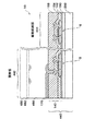
次に、図3に示すように、薄膜デバイス層140の上(第1の基材100とは反対側)に接着層160を介して第2の基材180を接着する。
【0034】
接着層160を構成する接着剤の好適な例としては、反応硬化型接着剤、熱硬化型接着剤、紫外線硬化型接着剤等の光硬化型接着剤、嫌気硬化型接着剤等の接着剤が挙げられる。この接着剤の組成としては、例えば、エポキシ系、アクリレート系、シリコーン系等、いかなるものでもよい。このような接着層160の形成は、例えば塗布法によりなされる。
【0035】
接着層160に硬化型接着剤を用いる場合には、例えば薄膜デバイス層140上に接着剤を塗布し、その上に第2の基材180を接合した後、接着剤の特性に応じた硬化方法により接着剤を硬化させて薄膜デバイス層140と第2の基材180とを接着固定する。
【0036】
接着層160に光硬化型接着剤を用いた場合には、例えば薄膜デバイス層140上に接着剤を塗布し、その上に第2の基材180を接合した後、光透過性の第1の基材100の側または光透過性の第2の基材180の側のうちの一方の側から接着剤に光を照射することにより接着剤を硬化させて薄膜デバイス層140と第2の基材180とを接着固定する。なお、光透過性の第1の基材100の側、および光透過性の第2の基材180の側の双方から接着剤に光を照射してもよい。ここで用いる接着剤としては、薄膜デバイス層140に影響を与えにくい紫外線硬化型等の接着剤が望ましい。
【0037】
接着層160としては水溶性接着剤を用いることもできる。この種の水溶性接着剤として、例えばケミテック株式会社製のケミシール U−451D(商品名)、株式会社スリーボンド製のスリーボンド3046(商品名)等を挙げることができる。
【0038】
薄膜デバイス層140の側に接着層160を形成する代わりに、第2の基材180の側に接着層160を形成し、この接着層160を介して、薄膜デバイス層140に第2の基材180を接着してもよい。第2の基材180自体が接着機能を有する場合等には、接着層160の形成を省略してもよい。
【0039】
第2の基材180は、第1の基材100と比較して、耐熱性や耐食性等といった特性が劣るものであってもよい。すなわち、本発明では、第1の基材100の側に薄膜デバイス層140を形成した後、この薄膜デバイス層140を第2の基材180に転写するため、第2の基材180には、薄膜デバイス層140を形成する際の温度条件に耐え得ること等といった特性が要求されない。従って、薄膜デバイス層140の形成の際の最高温度をTmaxとしたとき、転写体140を構成する材料としては、ガラス転移点(Tg)または軟化点がTmax以下のものを用いることができる。例えば、第2の基材180は、ガラス転移点(Tg)または軟化点が800℃以下あるいは500℃以下のものを用いることができ、さらには320℃以下のものであってもよい。
【0040】
第2の基材180の機械的特性としては、製造する機器の種類によっては、ある程度の剛性(強度)を有するものが用いられるが、可撓性、弾性を有するものであってもよい。
【0041】
第2の基材180としては、例えば、融点がそれほど高くない安価なガラス基板、シート状の薄いプラスチック基板、あるいはかなり厚めのプラスチック基板など、製造する機器の種類によって最適なものが用いられる。また、第2の基材180は、平板でなく、湾曲しているものであってもよい。
【0042】
第2の基材180としてプラスチック基板を用いる場合に、それを構成する合成樹脂としては、熱可塑性樹脂、熱硬化性樹脂のいずれでもよい。例えば、ポリエチレン、ポロプロピレン、エチレン−プレピレン共重合体、エチレン−酢酸ビニル共重合体(EVA)等のポリオレフィン、環状ポリオレフィン、変性ポリオレフィン、ポリ塩化ビニル、ポリ塩化ビニリデン、ポリスチレン、ポリアミド、ポリイミド、ポリアミドイミド、ポリカーボネート、ポリー(4−メチルベンテン−1)、アイオノマー、アクリル系樹脂、ポリメチルメタクリレート、アクリル−スチレン共重合体(AS樹脂)、ブタジエン−スチレン共重合体、ポリオ共重合体(EVOH)、ポリエチレンテレフタレート(PET)、ポリプチレンテレフタレート(PBT)、プリシクロヘキサンテレフタレート(PCT)等のポリエステル、ポリエーテル、ポリエーテルケトン(PEK)、ポリエーテルエーテルケトン(PEEK)、ポリエーテルイミド、ポリアセタール(POM)、ポリフェニレンオキシド、変形ポリフェニレンオキシド、ポリアリレート、芳香族ポリエステル(液晶ポリマー)、ポリテトラフルオロエチレン、ポリフッ化ビニリデン、その他フッ素系樹脂、スチレン系、ポリオレフィン系、ポリ塩化ビニル系、ポリウレタン系、フッ素ゴム系、塩素化ポリエチレン系等の各種熱可塑性エラストマー、エポキシ樹脂、フェノール樹脂、ユリア樹脂、メラミン樹脂、不飽和ポリエステル、シリコーン樹脂、ポリウレタン等、またはこれらを主とする共重合体、ブレンド体、ポリマーアロイ等が挙げられ、これらのうち1種、または2種以上を積層した積層体を用いることができる。
【0043】
第2の基材180としてプラスチック基板を用いた場合には、大型の第2の基材180を一体的に成形することができる。また、第2の基材180がプラスチック基板であれば、湾曲面や凹凸を有するもの等、複雑な形状であっても容易に製造することができる。さらに、第2の基材180がプラスチック基板であれば、材料コストや製造コストが低く済むという利点もある。それ故、第2の基材180がプラスチック基板であれば、大型で安価なデバイス(例えば、液晶表示装置)を製造する際に有利である。
【0044】
第2の基材180としてガラス基板を用いる場合には、それを構成するガラス材としては、例えば、ケイ酸ガラス(石英ガラス)、ケイ酸アルカリガラス、ソーダ石灰ガラス、カリ石灰ガラス、鉛(アルカリ)ガラス、バリウムガラス、ホウケイ酸ガラス等が挙げられる。このうち、ケイ酸ガラス以外のものは、ケイ酸ガラスと比較して融点が低いが、成形や加工等が比較的容易であり、かつ、安価であるので、好ましい。
【0045】
本形態において、第2の基材180は、例えば、アクティブマトリクス型液晶表示装置(電気光学装置)のアクティブマトリクス基板を薄膜デバイス装置として構成した場合のように、それ自体が独立してデバイスの基体を構成するものや、例えばカラーフィルタ、電極層、誘電体層、絶縁層、半導体素子のように、デバイスの一部を構成するものであってもよい。
【0046】
さらに、第2の基材180は、金属、セラミックス、石材、木材紙等の物質であってもよいし、ある品物を構成する任意の面上、例えばプリント基板の上等であってもよい。
【0047】
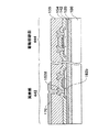
(第4の工程)
次に、図4に示すように、基板100の裏面側からエネルギー光を照射する。この工程では、エネルギー光として、例えばレーザ光を用いる。基板100の裏面側から照射されたレーザ光は、第1の基材100を透過した後に第1の分離層120に届く。これにより、第1の分離層120に層内剥離または界面剥離の一方、あるいは双方が生じる。
【0048】
従って、図5に示すように、第1の基材100を剥がすように力を加えると、第1の基材100を第1の分離層120で容易に剥がすことができる。その結果、薄膜デバイス層140を第2の基材180の方に転写することができる。この工程において、レーザ光の照射によって第1の分離層120において層内剥離や界面剥離が生じる原理は、レーザ光の照射によって第1の分離層120を構成する水素含有のアモルファスシリコン膜がポリシリコン膜に相転移するとともに、アモルファスシリコン膜から水素ガスが放出されることによるものである。
【0049】
第1の基材100を剥がした後には、薄膜デバイス層140の側に第1の分離層120が残ることがある。このような場合には、図6に示すように、残存している分離層120を、例えば洗浄、エッチング、アッシング、研磨等の方法またはこれらを組み合わせた方法により除去する。また、剥がした第1の基材100に第1の分離層120の一部が付着している場合にも同様に除去すれば、第1の基材100が石英ガラスのような高価な材料、希少な材料で構成されている場合に第1の基材100を再利用(リサイクル)することにより、製造コストの低減を図ることができる。
【0050】
この工程にて照射されるエネルギー光としては、第1の分離層120で層内剥離または界面剥離を起こさせるものであればいかなるものでもよく、例えば、紫外線、可視光、赤外線(熱線)等が挙げられる。その中でも、第1の分離層120に相転移や水素ガスの放出を生じさせ易いという点ではレーザ光が好ましい。
【0051】
レーザ光としては、各種気体レーザ、固体レーザ(半導体レーザ)等が挙げられるが、エキシマレーザ、Nd−YAGレーザ、Arレーザ、CO2レーザ、COレーザ、He−Neレーザ等が好適に用いられ、その中でもエキシマレーザが特に好ましい。このエキシマレーザは、短波長域で高エネルギーを出力するため、極めて短時間で第1の分離層120に相転移や水素ガスの放出を生じさせることができる。従って、レーザ光を照射したとき、第1の基材100や第2の基材180等に温度上昇をほとんど生じさせることがないので、第1の基材100や第2の基材180等を劣化あるいは破損させることなく、第1の分離層120で剥離することができる。
【0052】
図7に示すように、本形態で用いた第1の基材100は、300nm以上の波長に対して透過率が急峻に増大する特性を有する。従って、このような場合には、300nm以上の波長の光、例えば、Xe−Clエキシマレーザー光(波長308nm)等を照射する。
【0053】
このようにして、第1の基材100の裏面側からレーザ光を照射してアモルファスシリコン膜(第1の分離層120)をアニールすると、図8に示すように、アモルファスシリコン膜(α−Si)は、ポリシリコン膜(Poly−Si)に転移する。但し、あまりにエネルギー密度の高い光を照射すると、第1の分離層120を構成するシリコン膜が損傷して荒れた状態(アブレーション)にまでなってしまい、薄膜デバイス層140を損傷させてしまう。一方、エネルギー密度の低いレーザ光の照射では、アモルファスシリコン膜からポリシリコン膜への転移や水素ガスの発生がスムーズに起こらず、第1の分離層120での剥離が適正に進まない。また、図8において、レーザ光を照射したときシリコン膜が損傷しない領域と、シリコン膜にアブレーションが発生して損傷してしまう領域との境界を実線Lで示すように、シリコン膜を損傷させてしまうエネルギー密度のレベルは、シリコン膜中の水素量によって変化する。すなわち、水素含有量が高いシリコン膜であるほど、シリコン膜を損傷させてしまうエネルギー密度のレベルが低く、水素含有量が低いシリコン膜であるほど、シリコン膜を損傷させてしまうエネルギー密度のレベルが高い。そこで、本形態では、第1の分離層120に対するエネルギー光の照射を開始した初期の段階では、第1の分離層120を構成するシリコン膜に含まれる水素量が多いので、シリコン膜が損傷しないように、例えば150mJ/cm2くらいのエネルギー密度の低い光を照射し、このエネルギー光の照射によってシリコン膜から水素ガスが抜けた後は、例えば350mJ/cm2くらいのエネルギー密度の高い光を照射する。
【0054】
このような条件でレーザ光を照射する方法としては、エネルギー光のエネルギー密度を連続的、あるいは段階的に変化させてもよい。
【0055】
例えば、図9(a)、(b)に模式的に示すように、第1の基材100の面内方向で直交するX方向およびY方向のうち、X方向に延びるラインビーム(レーザ光)のY方向におけるエネルギー強度のプロファイルをガウシアン分布を有するように設定し、かつ、このラインビームをY方向に少しずつずらしていく。このような方法を採用すると、第1の分離層120からみれば、いずれの箇所も所定の時間、レーザ光の照射を連続して受けるが、その間、エネルギー強度は、図9(b)に矢印LAで示すエネルギー強度のプロファイルに沿って変化する。従って、第1の分離層120のいずれの箇所も、最初はエネルギー強度がかなり低いレーザ光の照射を受け、そのうちに、150mJ/cm2くらいのエネルギー密度の低いレーザ光を受けた後、350mJ/cm2くらいのエネルギー密度の高いレーザ光を受けることになる。
【0056】
また、図10(a)、(b)に模式的に示すように、第1の基材100の面内方向で直交するX方向およびY方向のうち、X方向に延びるラインビーム(レーザ光)のY方向におけるエネルギー強度のプロファイルを矩形形状あるいは台形形状の分布を有するように設定し、かつ、このラインビームをY方向にずらしていく。そして、基板全面へのレーザ光の照射が終われば、同一の基板に対して同様なレーザ照射を繰り返す。その際には、図10(a)、(b)に示すように、エネルギー強度を段階的に高めていく。その結果、1回目の照射時には、150mJ/cm2くらいのエネルギー密度の低いレーザ光を受け、最後には350mJ/cm2くらいのエネルギー密度の高いレーザ光を受けることになる。
【0057】
第1の基材100の裏面側からレーザ光を照射したとき、第1の分離層120を透過した照射光が薄膜デバイス層140にまで達して悪影響を及ぼす場合の対策としては、例えば、図11に示すように、レーザ光を吸収する第1の分離層120上にタンタル(Ta)等の金属膜124を形成する方法がある。この方法によれば、第1の分離層120を透過したレーザー光は、金属膜124の界面で完全に反射されるので、それより上層に形成された薄膜デバイス層140に悪影響を与えない。
【0058】
以上の各工程を経て、薄膜デバイス層140の第2の基材180への転写が完了し、第2の基材180上に薄膜デバイス層140が転写された薄膜デバイス装置1を製造することができる。また、薄膜デバイス層140が形成された第2の基材180を所望の材料上に搭載したものを薄膜デバイス装置としてもよい。
【0059】
なお、第1の基材100から第2の基材180に薄膜デバイス層140を転写した後は、必要に応じて、薄膜デバイスに隣接する不要なSiO2膜などを除去する。また、第1の基材100から第2の基材180に薄膜デバイス層140を転写した後、この第2の基板180上で薄膜デバイス層140に対する配線用の導電層や保護膜の形成を行ってもよい。
【0060】
このように、本形態の薄膜デバイス装置1の製造方法では、被剥離物である薄膜デバイス層140自体を直接に剥離するのではなく、薄膜デバイス層140と第1の基材100とを第1の分離層120で剥がす。このため、薄膜デバイス層140の側から第1の基材100を容易、かつ、確実に剥がすことができる。従って、剥離操作に伴う薄膜デバイス層140へのダメージがなく、信頼性の高い薄膜デバイス装置1を製造することができる。
【0061】
また、本形態では、第4の工程において、レーザ光を照射していくうちに第1の分離層120を構成するシリコン膜の性質が変化していくのに合わせてエネルギー密度を低密度から高密度に変化させるので、第1の分離層120を構成するシリコン膜が損傷しない範囲内で、エネルギー密度の高いレーザ光を照射することができる。それ故、第1の分離層120の層内あるいは界面での剥離をスムーズに、かつ、確実に進行させることができる。よって、本形態によれば、信頼性の高い薄膜デバイス装置1を効率よく製造できる。
【0062】
[第2の実施の形態]
図12ないし図14を参照して、本発明の第2の実施の形態を説明する。
【0063】
図12ないし図14はいずれも、本形態の薄膜デバイス装置の製造方法のうち、第1の実施の形態と略同様、第4の工程で薄膜デバイス層140を第2の基材に転写した後に行う各工程の様子を示す工程断面図である。
【0064】
本形態は、実施の形態1で説明した第4の工程の後、薄膜デバイス層140を第2の基材180から第3の基材に再度、転写することに特徴を有し、第1の実施の形態と略同様な方法で第2の基材180への薄膜デバイス層140の転写を行う。従って、本形態でも、第1の実施の形態に関して説明した第1ないし第4の工程を略同様に行うので、これらの工程については、詳細な説明を省略する。
【0065】
本形態でも、図1(a)に示すように、第1の基材100上に、水素を含有するアモルファスシリコン膜からなる第1の分離層120を形成した後(第1の工程)、図2に示すように、この第1の分離層120上に薄膜デバイス層140を形成する(第2の工程)。次に、図3に示すように、薄膜デバイス層140の第1の基材100と反対側に第2の基材180を接着する(第3の工程)。本形態では、後述するように、第2の基材180も薄膜デバイス層140の側から剥がすので、接着層160に代えて、図12を参照して後述するように、第2の基材180を第2の分離層160′を介して薄膜デバイス層140に接着する。この第2の分離層160′としては、熱溶融性接着剤や水溶性接着剤などの接着剤を用いることができる。以下の説明では、第2の分離層160′を熱溶融性接着剤によって形成した例を説明する。次に、図4ないし図6に示すように、第1の分離層120にレーザ光などのエネルギー光を照射して第1の分離層120で剥離現象を起こさせ、薄膜デバイス層140を第2の基材180に転写する(第4の工程)。この第4の工程では、第10の分離層に照射するレーザ光のエネルギー密度を低密度から高密度に変化させる。
【0066】
(第5の工程)
このようにして、薄膜デバイス層140を第2の基材180に転写した後は、図12に示すように、薄膜デバイス層140の下面(第2の基材180と反対側)に接着層190を介して第3の基材200を接着する。この接着層190を構成する接着剤の好適な例としては、反応硬化型接着剤、熱硬化型接着材、紫外線硬化型接着剤等の光硬化型接着剤、嫌気硬化型接着剤等の各種の硬化型の接着剤が挙げられる。接着剤の組成としては、例えば、エポキシ系、アクリレート系。シリコーン系等、いかなるものでもよい。このような接着層190の形成は、例えば塗布法によりなされる。
【0067】
接着層190として硬化型接着剤を用いる場合、例えば薄膜デバイス層140の下面に硬化型接着剤を塗布した後、第3の基材200を接合し、しかる後に、硬化型接着剤の特性に応じた硬化方法により硬化型接着剤を硬化させて、薄膜デバイス層140と第3の基材200とを接着固定する。
【0068】
接着層190として光硬化型接着剤を用いる場合、好ましくは光透過性の第3の基材200の裏面側から光を照射する。接着剤としては、薄膜デバイス層140に影響を与えにくい紫外線硬化型等の接着剤を用いれば、光透過性の第2の基材180側から光を照射してもよいし、第2の基材180の側および第3の基材200の側の双方から光を照射してもよい。なお、第3の基材200に接着層190を形成し、その上に薄膜デバイス層140を接着しても良い。また、第3の基材200自体が接着機能を有する場合等には、接着層190の形成を省略しても良い。
【0069】
第2の基材180および第3の基材200は、第1の基材100と比較して、耐熱性や耐食性等といった特性が劣るものであってもよい。すなわち、本形態では、第1の基材100の側に薄膜デバイス層140を形成した後、この薄膜デバイス層140を第2の基材180に転写し、しかる後に第3の基材200に転写するため、第2の基材180および第3の基材200には、薄膜デバイス層140を形成する際の温度条件に耐え得ること等といった特性が要求されない。従って、薄膜デバイス層140の形成の際の最高温度をTmaxとしたとき、第2の基材180および第3の基材200を構成する材料としては、ガラス転移点(Tg)または軟化点がTmax以下のものを用いることができる。例えば、第2の基材180は、ガラス転移点(Tg)または軟化点が800℃以下あるいは500℃以下のものを用いることができ、さらには320℃以下のものであってもよい。
【0070】
第3の基材200の機械的特性としては、製造する機器の種類によっては、ある程度の剛性(強度)を有するものが用いられるが、可撓性、弾性を有するものであってもよい。
【0071】
第3の基材200としては、例えば、融点がそれほど高くない安価なガラス基板、シート状の薄いプラスチック基板、あるいはかなり厚めのプラスチック基板など、製造する機器の種類によって最適なものが用いられる。また、第3の基材200は、平板でなく、湾曲しているものであってもよい。
【0072】
第3の基材200としてプラスチック基板を用いる場合に、それを構成する合成樹脂としては、熱可塑性樹脂、熱硬化性樹脂のいずれでもよい。例えば、ポリエチレン、ポロプロピレン、エチレン−プレピレン共重合体、エチレン−酢酸ビニル共重合体(EVA)等のポリオレフィン、環状ポリオレフィン、変性ポリオレフィン、ポリ塩化ビニル、ポリ塩化ビニリデン、ポリスチレン、ポリアミド、ポリイミド、ポリアミドイミド、ポリカーボネート、ポリー(4−メチルベンテン−1)、アイオノマー、アクリル系樹脂、ポリメチルメタクリレート、アクリル−スチレン共重合体(AS樹脂)、ブタジエン−スチレン共重合体、ポリオ共重合体(EVOH)、ポリエチレンテレフタレート(PET)、ポリプチレンテレフタレート(PBT)、プリシクロヘキサンテレフタレート(PCT)等のポリエステル、ポリエーテル、ポリエーテルケトン(PEK)、ポリエーテルエーテルケトン(PEEK)、ポリエーテルイミド、ポリアセタール(POM)、ポリフェニレンオキシド、変形ポリフェニレンオキシド、ポリアリレート、芳香族ポリエステル(液晶ポリマー)、ポリテトラフルオロエチレン、ポリフッ化ビニリデン、その他フッ素系樹脂、スチレン系、ポリオレフィン系、ポリ塩化ビニル系、ポリウレタン系、フッ素ゴム系、塩素化ポリエチレン系等の各種熱可塑性エラストマー、エポキシ樹脂、フェノール樹脂、ユリア樹脂、メラミン樹脂、不飽和ポリエステル、シリコーン樹脂、ポリウレタン等、またはこれらを主とする共重合体、ブレンド体、ポリマーアロイ等が挙げられ、これらのうち1種、または2種以上を積層した積層体を用いることができる。
【0073】
第3の基材200としてプラスチック基板を用いた場合には、大型の第3の基材200を一体的に成形することができる。また、第3の基材200がプラスチック基板であれば、湾曲面や凹凸を有するもの等、複雑な形状であっても容易に製造することができる。さらに、第3の基材200がプラスチック基板であれば、材料コストや製造コストが低く済むという利点もある。それ故、第3の基材200がプラスチック基板であれば、大型で安価なデバイス(例えば、液晶表示装置)を製造する際に有利である。
【0074】
第3の基材200としてガラス基板を用いる場合には、それを構成するガラス材としては、例えば、ケイ酸ガラス(石英ガラス)、ケイ酸アルカリガラス、ソーダ石灰ガラス、カリ石灰ガラス、鉛(アルカリ)ガラス、バリウムガラス、ホウケイ酸ガラス等が挙げられる。このうち、ケイ酸ガラス以外のものは、ケイ酸ガラスと比較して融点が低いが、成形や加工等が比較的容易であり、かつ、安価であるので、好ましい。
【0075】
本形態において、第3の基材200は、例えば、アクティブマトリクス型液晶表示装置(電気光学装置)のアクティブマトリクス基板を構成する場合のように、それ自体独立したデバイスを構成するものや、例えばカラーフィルタ、電極層、誘電体層、絶縁層、半導体素子のように、デバイスの一部を構成するものであってもよい。
【0076】
さらに、第3の基材200は、金属、セラミックス、石材、木材紙等の物質であってもよいし、ある品物を構成する任意の面上、例えばプリント基板の上等であってもよい。
【0077】
(第6の工程)
次に、図13に示すように、熱溶融性接着剤からなる第2の分離層160′を加熱し、熱溶融させる。この結果、第2の分離層160′の接着力が弱まるため、第2の基材180を薄膜デバイス層140の側から剥がすことができる、この第2の基材180についても、付着した熱溶融性接着剤を除去することで、繰り返し使用することができる。また、第2の分離層160′として水溶性接着剤を用いた場合には、少なくとも第2の分離層160′を含む領域を純水に浸せばよい。
【0078】
次に、図14に示すように、薄膜デバイス層140の表面に残る第2の分離層160′を除去する。その結果、第3の基材200に薄膜デバイス層140が転写された薄膜デバイス装置1を製造することができる。
【0079】
なお、第1の基材100から第2の基材180に薄膜デバイス層140を転写した後は、必要に応じて、薄膜デバイスに隣接する不要なSiO2膜などを除去する。また、第1の基材100から第2の基材180に薄膜デバイス層140を転写した後、あるいは第2の基材180から第3の基材200に薄膜デバイス層140を転写した後、第2の基材200あるいは第3の基材200上で薄膜デバイス層140に対する配線等の導電層や保護膜の形成等を行ってもよい。
【0080】
このように、本形態の薄膜デバイス装置1の製造方法では、第4の工程において、レーザ光を照射していくうちに第1の分離層120を構成するシリコン膜の性質が変化していくのに合わせてエネルギー密度を低密度から高密度に変化させるので、第1の分離層120を構成するシリコン膜が損傷しない範囲内で、エネルギー密度の高いレーザ光を照射することができるなど、実施の形態1と同様な効果を奏する。また、本形態では、薄膜デバイス層140を2回、転写するので、第3の基材200上での薄膜デバイス層140の積層関係は、図2に示すように第1の基材100上に薄膜デバイス層140を形成したときの積層関係と同じである。
【0081】
[その他の実施の形態]
なお、上記の第1および第2の実施の形態のいずれにおいても、プラズマCVD法(425℃)により形成した水素含有のアモルファスシリコン膜を第1の分離層120として用いたが、水素を含有しないアモルファスシリコン、あるいは水素を少量だけ含有するアモルファスシリコンを形成した以降、図4および図5に示す剥離工程を行う前の所定の時期に水素イオンを導入したアモルファスシリコン膜を第1の分離層120として用いてもよい。
【0082】
[第1の実施例]
本発明の第1の実施の形態の具体例として、図15ないし図25を参照して、第1の基材100の側に、CMOS構造のTFT(薄膜デバイス)を含む薄膜デバイス層140を形成し、このデバイス層140を第2の基材180に転写した薄膜デバイス装置の製造方法を説明する。図15ないし図25は、この製造方法の工程断面図である。
【0083】
(第1の工程)
図15に示すように、本例では、石英基板などの透光性の基板からなる第1の基材100上に、水素含有のアモルファスシリコン膜からなる第1の分離層120を形成する。本例では、縦50mm×横50mm×厚さ1.1mmの石英基板(軟化点:1630℃、歪点:1070℃、エキシマレーザの透過率:ほぼ100%)からなる第1の基材100を用意し、この第1の基材100の片面に対して、原料ガスとしてSi2H6ガスを用いたプラズマCVD法(425℃)により、膜厚が1000nmの水素含有のアモルファスシリコン膜からなる第1の分離層120を形成する。
【0084】
(第2の工程)
次に、第1の分離層120の上に、プラズマCVD法(SiH4+O2ガス、100℃)により、膜厚が2000nmのSiO2膜からなる中間層142を形成する。
【0085】
次に、中間層142の上に、LPCVD法(Si2H6ガス、425℃)により膜厚が50nmアモルファスのシリコン膜143を形成する。このシリコン膜143はTFTの能動層を形成するための半導体膜である。
【0086】
次に、第1の基材100においてシリコン膜143が形成されている側から、波長が308nmのレーザー光を照射し、シリコン膜143にレーザアニールを施す。これにより、シリコン膜143は、再結晶化してアモルファスシリコン膜からポリシリコン膜となる。ここで行うレーザ光の照射は、第4の工程において第1の分離層120で剥離現象を起こさせるために照射するレーザ光と比較してエネルギー密度はかなり低い。
【0087】
次に、図16に示すように、シリコン膜143をパターニングして、チャネルパターンとしてアイランド144a、144bを形成する。
【0088】
次に、図17に示すように、TEOS−CVD法(SiH4+O2ガス)により、膜厚が1200nmのSiO2からなるゲート絶縁膜148を形成する。
【0089】
次に、図18に示すように、ポリシリコン膜あるいは金属等からなるゲート電極150a、150bを形成する。
【0090】
次に、図19に示すように、アイランド144aを覆うようにポリイミド等からなるマスク層170を形成し、この状態で、例えばボロン(b)のイオン注入を行う。これによって、アイランド144bには、ゲート電極150bに対してセルフアライン的にP+層172a、172b(ソース・ドレイン領域)が形成される。このボロンイオン注入工程では、例えば、B2H6(5%)+H2(95%)の混合ガスをプラズマ化し、それにより生成されたボロンイオン及び水素イオンを加速して、質量分析器を介さずにイオン導入を行うと、同じ加速電圧であっても、質量の重いボロンイオンは上層側のポリシリコン膜(アイランド144b)に止まる一方で、質量の軽い水素イオンはより深く打ち込まれて、第1の分離層120まで到達する。
【0091】
次に、図20に示すように、アイランド144bを覆うようにポリイミド等からなるマスク層174を形成し、この状態で、例えば、リン(P)のイオン注入を行う。これによって、アイランド144aには、ゲート電極150aに対してセルフアライン的にn+層146a、146b(ソース・ドレイン領域)が形成される。この場合にも、例えばPH3(5%)+H2(95%)の混合ガスをプラズマ化し、それにより生成されたリンイオン及び水素イオンを加速して、質量分析器を介ざずにイオン導入を行うと、同じ加速電圧であっても、質量の重いリンイオンは、上層側のポリシリコン膜(アイランド144a)に止まる一方で、質量の軽い水素イオンはよ深く打ち込まれて、第1の分離層120まで到達する。
【0092】
次に、図21に示すように、層間絶縁膜154を形成した後、この層間絶縁膜154を選択的にエッチングしてコンタクトホールを形成した後、ソース・ドレイン電極152a、152b、152c、152dを形成する。
【0093】
このようにして、CMOS構造のTFTを備えた薄膜デバイス層140が形成される。なお、層間絶縁層154上にはさらに保護膜を形成してもよい。
【0094】
(第3の工程)
次に、図22に示すように、CMOS構成のTFTを備える薄膜デバイス層140の上に接着層としてのエポキシ樹脂からなる接着層160を形成した後、この接着層160を介して、薄膜デバイス層140に対して、縦200mm×横300mm×厚さ1.1mmのソーダガラスからなる第2の基材180を貼り付ける。次に、接着層160に熱を加えてエポキシ樹脂を硬化させ、第2の基材180と薄膜デバイス層140の側とを接着する。なお、接着層160は紫外線硬化型接着剤でもよい。この場合には、第2の基材180側から紫外線を照射してポリマーを硬化させる。
【0095】
(第4の工程)
次に、図23に示すように、透光性基板からなる第1の基材100の裏面から、例えば、波長が308nmのXe−Clエキシマレーザー光を照射する。照射されたレーザ光は、第1の基材100を透過して第1の分離層120に届く。この工程では、第1の分離層120に対するエネルギー光の照射を開始した初期の段階では、第1の分離層120を構成するシリコン膜に含まれる水素量が多いので、シリコン膜が損傷しないように、例えば150mJ/cm2くらいのエネルギー密度の低い光を照射し、このエネルギー光の照射によってシリコン膜から水素ガスが抜けた後は、例えば350mJ/cm2くらいのエネルギー密度の高い光を照射する。その結果、第1の分離層120を構成する水素含有のアモルファスシリコン膜では、ポリシリコン膜への層転移と、水素ガスの発生が起こり、第1の分離層120の層内および/または界面において剥離が生じる。
【0096】
なお、エキシマレーザの照射は、スポットビーム照射とラインビーム照射のいずれをも用いることができる。スポットビーム照射の場合は、所定の単位領域(例えば8mm×8mm)にスポット照射しこのスポット照射を、各回の照射条件を変え、かつ、照射領域が重ならないようにビーム走査しながら照射していく。また、ラインビーム照射の場合は、所定の単位領域(例えば、378mm×0.1mmや0.3mmを同じく、各回の照射領域を少しずつ重ねながら、あるいは完全にずらしながらビーム走査していく。
【0097】
このようにして第1の分離層120で剥離現象を起こさせてから、図24に示すように、薄膜デバイス層140の側から第1の基材100を剥がす。その結果、薄膜デバイス層140は第2の基材180に転写される。
【0098】
次に、薄膜デバイス層140の裏面側に残る第1の分離層120をエッチングにより除去する。その結果、図25に示すように、CMOS構成のTFTが第2の基材180に転写された薄膜デバイス装置1が完成する。
【0099】
このようにして製造された薄膜デバイス装置1は、例えば、図26(a)に示すように、プラスチック等からなるフレキシブル基板182上に搭載される。その結果、薄膜デバイス装置1によって回路が構成されたCPU300、RAM320、入出力回路360、並びにこれらの回路に電源供給するための太陽電池340がフレキシブル基板180上に搭載されたマイクロコンピュータを製造することができる。このように構成したマイクロコンピュータは、フレキシブル基板182上に形成されているため、図26(b)に示すように曲げに強く、また、軽量であるために落下にも強いという利点がある。
【0100】
[第1の実施例の変形例1]
本発明の第1の実施例では、第1の基材100上に、水素含有のアモルファスシリコン膜からなる第1の分離層120をプラズマCVD法(425℃)により形成したが、LPCVD法によって成膜しても、2%程度の水素を含有するアモルファスシリコン膜を形成することができるので、このLPCVD法で形成したアモルファスシリコン膜を第1の分離層120として用いてもよい。
【0101】
[第1の実施例の変形例2]
本発明の第1の実施例では、第1の工程において、第1の基材100上に、水素含有のアモルファスシリコン膜からなる第1の分離層120をプラズマCVD法(425℃)により形成したが、本例では、水素を含有しないアモルファスシリコン、あるいは水素を少量だけ含有するアモルファスシリコンを形成した以降、このシリコン膜に別途、水素イオンを導入したアモルファスシリコン膜を第1の分離層120として用いる。すなわち、本例でも、第1の実施例と同様、図15ないし図25を参照して説明した各工程を行うが、本例では、図15に示す第1の工程において、第1の基材100上に、たとえばLPCVD法により、水素を含有しないアモルファスシリコン、あるいは水素を少量だけ含有するアモルファスシリコンを形成する。その代わりに、第1の工程でアモルファスシリコン膜(第1の分離層120)を形成した以降、図23に示す第4の工程でレーザ光を照射して分離層で剥離を起こさせる以前に、第1の分離層120に水素イオンを導入する。
【0102】
ここで、第1の分離層120に対する水素イオンの導入は、たとえば以下のタイミングで行う。
【0103】
まず、第1の例として、図15に示す第1の工程で第1の分離層120を形成すべきアモルファスシリコン膜を形成した後、中間層142を形成する前に水素イオンをイオン注入、あるいはイオンドーピングによりアモルファスシリコン膜に導入する。
【0104】
また、第2の例として、図15に示す第1の工程で第1の分離層120を形成した後、第2の工程で中間層142を形成し、しかる後に、水素イオンをイオン注入、あるいはイオンドーピングによりアモルファスシリコン膜に導入してもよい。このようなタイミングで水素イオンを導入すれば、比較的高いエネルギーで効率よく水素イオンを導入することができるので、中間層142を形成する前に水素イオンを導入する方法(第1の例)と比較して短時間で処理を終えることができる。
【0105】
さらに、第3の例として、図15に示す第1の工程で第1の分離層120を形成した後、第2の工程で中間層142、およびTFTの能動層を形成すべきシリコン膜143を形成した以降、レーザアニールによる結晶化工程を行う前に、水素イオンをイオン注入、あるいはイオンドーピングによりアモルファスシリコン膜に導入してもよい。このように構成すると、シリコン膜143をたとえば425℃位の温度で形成した際に、第1の分離層120に含まれていた水素が脱離すすることを防止することができる。また、結晶化工程前に水素イオンを導入しておけば、水素イオンの導入によって発生したダメージをこの結晶化工程で修復することができる。
【0106】
[第2の実施例]
本発明の第1の実施の形態の具体例として、図27ないし図34を参照して、第1の基材100の側に各種のTFTを含む薄膜デバイス層140を形成し、これを第2の基材180に転写して液晶表示装置(電気光学装置)のアクティブマトリクス基板(薄膜デバイス装置)の製造方法を説明する。図27は液晶表示装置の全体構成を示す分解斜視図である。図28は、この液晶表示装置に用いたアクティブマトリクス基板の構成を示すブロック図である。図29は、本形態の液晶表示装置の要部を示す断面図である。
【0107】
図27において、本形態の液晶表示装置10は、アクティブマトリクス基板440と、このアクティブマトリクス基板440に所定の間隔を介して貼り合わされた対向基板480と、この対向基板480とアクティブマトリクス基板440との間に封入された液晶460とから概略構成されている。アクティブマトリクス基板440と対向基板480とは、対向基板480の外周縁に沿って形成されたギャップ材含有のシール材(図示せず。)によって所定の間隙を介して貼り合わされ、このシール材の内側領域が液晶460の封入領域とされる。シール材としては、エポキシ樹脂や各種の紫外線硬化樹脂などを用いることができる。ここで、シール材は部分的に途切れているので、対向基板480とアクティブマトリクス基板440とを貼り合わせた後、シール材の内側領域を減圧状態にすれば、シール材の途切れ部分から液晶460を減圧注入でき、液晶460を封入した後は、途切れ部分を封止剤(図示せず。)で塞げばよい。
【0108】
本形態において、対向基板480はアクティブマトリクス基板440よりも小さく、アクティブマトリクス基板440の対向基板480の外周縁よりはみ出た領域には、図28を参照して後述する走査線駆動回路700やデータ線駆動回路800等のドライバー部444が形成されている。
【0109】
また、対向基板480およびアクティブマトリクス基板440の光入射側の面あるいは光出射側には、使用する液晶の種類、すなわち、TN(ツイステッドネマティック)モード、STN(スーパーTN)モード等々の動作モードや、ノーマリホワイトモード/ノーマリブラックモードの別に応じて偏光板420、500、あるいは位相差フィルムが所定の光軸方向に配置されるように貼られる。さらに、液晶表示装置10が透過型である場合には、アクティブマトリクス基板440の裏側にはバックライト400が配置される。
【0110】
このように構成した液晶表示装置10に用いたアクティブマトリクス基板440では、図28に示すように、中央領域が実際の表示を行う画素部442であり、その周辺部分が駆動回路部444とされる。画素部442では、アルミニウム、タンタル、モリブデン、チタン、タングステンなどの金属膜、シリサイド膜、導電性半導体膜などで形成されたデータ線720および走査線730に接続した画素用スイッチングのTFT5がマトリクス状に配列された各画素毎に形成されている。データ線720に対しては、シフトレジスタ、レベルシフタ、ビデオライン、アナログスイッチなどを備えるデータ側駆動回路800が構成されている。走査線730に対しては、シフトレジスタおよびレベルシフタなどを備える走査側駆動回路700が構成されている。
【0111】
このように構成したアクティブマトリクス基板440において、データ線駆動回路800および走査線駆動回路700のシフトレジスタ等は、N型のTFT6とP型のTFT7とからなるCMOS回路が多段に接続されている。従って、アクティブマトリクス基板440には、駆動回路用のN型のTFT6、駆動回路用のP型のTFT7、および画素スイッチング用のN型のTFT5からなる3種類のTFTが形成されている。
【0112】
これらのTFTのうち、駆動回路用のN型のTFT6と駆動回路用のP型のTFT7とは導電型が逆であるだけで、基本的な構成が同一なので、図29には、代表して、N型のTFT6と画素スイッチング用のTFT5のみを示してある。
【0113】
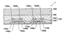
図29において、画素スイッチング用のTFT5では、画素電極170が液晶を介して対向基板480と対向させる必要があるが、本形態では、いずれのTFTも、後述するように、薄膜デバイス層140として第1の基材100に形成されたものが、第2の基材180に転写されたものであるため、画素電極170は、TFT5の最も上層側にある。そこで、本形態では、層間絶縁膜155に開口156、157を形成し、開口157から下方に向かって画素電極170が露出している構造になっている。従って、薄膜デバイス層140の裏面側に対して液晶460を介して対向基板480が対向する構成であっても、画素電極170と対向基板480に形成した共通電極482との間で液晶460を駆動することができる。なお、図28からわかるように、画素スイッチング用のTFT5において、ゲート電極150は走査線730の一部であり、ソース領域192aに電気的に接続するソース電極152eはデータ線720の一部である。なお、画素電極170は開口156を介してドレイン領域192bに電気的に接続している。
【0114】
図30ないし図34を参照して、このアクティブマトリクス基板440の製造方法を説明する。図30ないし図34は、前記した第1の実施の形態に係る方法を用いてアクティブマトリクス基板440を製造する際の工程断面図である。
【0115】
本例の液晶表示装置の製造方法のうち、そのアクティブマトリクス基板440の製造方法では、まず、図15ないし図25を参照して説明した方法と同様、図30に示すように、石英基板からなる第1の基材100上に、水素含有のアモルファスシリコン膜からなる第1の分離層120を形成する(第1の工程)。
【0116】
次に、第1の分離層120の上に中間層142を形成した後、その上に駆動回路用のTFT6および画素スイッチング用のTFT5を形成する(第2の工程)。
【0117】
次に、図31に示すように、画素スイッチング用のTFT5のドレイン領域192bに相当する部分、および画素スイチング用のTFT5が形成されている領域を除く領域のそれぞれにおいて、層間絶縁膜154、155、ゲート絶縁膜148および中間膜142を選択的にエッチングし、それぞれの領域に開口156、157を同時に形成する。
【0118】
次に、図32に示すように、画素電極170を形成する。その結果、画素電極170は、開口156をコンタトクトホールとして、ドレイン電極152dを介して画素スイッチング用のTFTのドレイン領域192bに電気的に接続し、かつ、開口157を介して第1の分離層120と接するように形成される。ここで、画素電極170をITO膜から形成した場合には液晶表示装置10を透過型で形成でき、画素電極170をアルミニウム等の金属から形成した場合には、液晶表示装置10を反射型で形成できる。
【0119】
次に、図33に示すように、接着層160を介して、ソーダガラス基板等といった安価な第2の基材180を接着する(第3の工程)。
【0120】
次に、第1の基材100の裏面側からエキシマレーザー光を照射し、第1の分離層120で剥離現象を生じさせ、第1の基材100を剥がす。このとき、引き剥がしにさほどの力を要しないので、TFT5、6等には機械的ダメージが生じない。また、薄膜デバイス層140の裏面側に残った第1の分離層120を除去する。
【0121】
これにより、図34に示すアクティブマトリクス基板440が完成する。このアクティブマトリクス基板440では、画素電極170が薄膜デバイス層140の裏面側で露出している。従って、アクティブマトリクス基板440の薄膜デバイス層140の裏面側に配向膜(図示せず。)を形成した後、ラビング処理等の配向処理を行い、しかる後に、図28に示すように、薄膜デバイス層140の裏面側と対向するように対向基板480をアクティブマトリクス基板440とシール材(図示せず。)によって貼り合わせ、これらの基板間に液晶460を封入する。その結果、アクティブマトリクス基板440と対向基板480との間に液晶460を挟持した液晶表示装置10を製造することができる。
【0122】
このように、本形態の液晶表示装置10に用いたアクティブマトリクス基板440では、耐熱性等に優れた石英基板からなる第1の基材100上にTFTを最適な条件で形成した後、この第1の基材100から、ソーダガラス基板からなる安価な第2の基材180の側に駆動回路用のTFT6や画素スイチング用のTFT4を含む薄膜デバイス層140を転写したものを用いている。このため、TFT5、6の製造時には第1の基材100の上で石英基板の耐熱性を十分に行かした温度条件でTFT5、6を形成できるので、トランジスタ特性の優れたTFT5、6を形成することができる。また、液晶表示装置10に実際に搭載されるのは、安価なソーダガラスからなる第2の基材180であるため、液晶用表示装置10の低価格化を図ることができる。
【0123】
[第3の実施例]
本発明の第2の実施の形態の具体例として、図35ないし図42を参照して、第1の基材100の側に薄膜デバイス層140として、第1の基材100にTFTを形成し、これを第2の基材180に転写した後、さらに第3の基材200に転写した液晶表示装置(電気光学装置)のアクティブマトリクス基板440の製造方法を説明する。図35は、本例の液晶表示装置10の要部を示す断面図である。なお、本形態の液晶表示装置10およびアクイティブマトリクス基板440の基本的な構成は、第2の実施例と同様、図27および図28を参照して説明したとおりであるので、それらの説明を省略する。
【0124】
図35において、本形態の液晶表示装置10は、アクティブマトリクス基板440と、このアクティブマトリクス基板440に所定の間隔を介して貼り合わされた対向基板480と、この対向基板480とアクティブマトリクス基板440との間に封入された液晶460とから概略構成されている。本例でも、アクティブマトリクス基板440には、駆動回路用のN型のTFT、駆動回路用のP型のTFT、および画素スイッチング用のN型のTFTからなる3種類のTFTが形成されているが、図35には、これらのTFTのうち、駆動回路用のN型のTFT6、および画素スイッチング用のTFT5のみを示してある。
【0125】
本例において、駆動回路用のTFT6および画素スイッチング用のTFT5は、いずれも、後述するように、薄膜デバイス層140として第1の基材100に形成されたものが、第2の基材180に転写された後、第3の基材200に転写されたものであるため、各TFT5、6は、第1の基材100上に形成したときの積層構造のままである。すなわち、画素電極170は、層間絶縁膜155の上層に形成され、対向基板480に形成した共通電極482との間で液晶460を駆動することができる。
【0126】
図36ないし図42を参照して、このアクティブマトリクス基板440の製造方法を説明する。図36ないし図42は、前記した第2の実施の形態に係る方法を用いてアクティブマトリクス基板440を製造する際の工程断面図である。
【0127】
本例の液晶表示装置10の製造方法のうち、そのアクティブマトリクス基板の製造方法では、まず、図15ないし図25を参照して説明した方法と同様、図36に示すように、石英基板からなる第1の基材100上に、水素含有のアモルファスシリコン膜からなる第1の分離層120を形成する(第1の工程)。
【0128】
次に、第1の分離層120の上に中間層142を形成した後、その上に駆動回路用のTFT6および画素スイッチング用のTFT5を形成する(第2の工程)。
【0129】
本例でも、画素スイッチング用のTFT5では、図28を参照して説明したように、ゲート電極150は走査線730の一部であり、ソース電極152eはデータ線720の一部である。
【0130】
次に、画素スイッチング用のTFT5のドレイン領域192bに相当する部分の上層に位置する層間絶縁膜154、155およびゲート絶縁膜148を選択的にエッチングし、開口156を形成する。
【0131】
次に、図37に示すように、画素電極170を形成する。その結果、画素電極170は、開口156をコンタトクトホールとして、ドレイン電極192bを介して画素スイッチング用のTFT5のドレイン領域192eに電気的に接続する。本例でも、画素電極170をITO膜から形成した場合には液晶表示装置10を透過型で形成でき、画素電極170をアルミニウム等の金属から形成した場合には、液晶表示装置10を反射型で形成できる。
【0132】
次に、図38に示すように、熱溶融性接着剤あるいは水溶性の接着剤などからなる第2の分離層160′を介して、ソーダガラス基板等といった安価な第2の基材180を接着する(第3の工程)。
【0133】
次に、第1の基材100の裏面側からエキシマレーザー光を照射し、第1の分離層120で剥離現象を生じさせ、薄膜デバイス層140の側から第1の基材100を剥がす。このとき、引き剥がしにさほどの力を要しないので、TFT5、6等には機械的ダメージが生じない。また、図39に示すように、薄膜デバイス層140の裏面側に付着している第1の分離層120を除去する。
【0134】
次に、図40に示すように、薄膜デバイス層140の裏面側に対して接着層190を介して第3の基材200を接着する。
【0135】
次に、第2の分離層160′として熱溶融性接着剤を用いた場合にはこの熱溶融性接着剤を加熱し、第2の分離層160′で第2の基材180を剥離する。水溶性接着剤を用いた場合にはこの水溶性接着剤を水と接触させて、第2の分離層160′で第2の基材180を剥離する。次に、図41に示すように、薄膜デバイス層140の表面側に付着している第2の分離層180を除去する。
【0136】
その結果、アクティブマトリクス基板440が完成する。次に、図35に示すように、画素電極170の表面および層間絶縁膜155の表面に対して配向膜(図示せず。)を形成した後、ラビング処理等の配向処理を行い、しかる後に、薄膜デバイス層140に対向するように対向基板480をアクティブマトリクス基板440とシール材(図示せず。)によって貼り合わせ、これらの基板間に液晶460を封入する。その結果、アクティブマトリクス基板440と対向基板480との間に液晶460を挟持した液晶表示装置10を製造することができる。
【0137】
このように、本形態に係る液晶表示装置10に用いたアクティブマトリクス基板440は、耐熱性等に優れた石英基板からなる第1の基材100上にTFTを最適な条件で形成した後、この第1の基材100から第2の基材180への転写を経て、ソーダガラス基板からなる安価な第3の基材200の側に、駆動回路用のTFTや画素スイチング用のTFTを含む薄膜デバイス層140を転写したものである。このため、TFTの製造時には第1の基材100上で石英基板の耐熱性を十分に行かした温度条件でTFTを形成できるので、トランジスタ特性の優れたTFTを形成することができる。また、液晶表示装置10に実際に搭載されるのは、安価なソーダガラスからなる第3の基材200であるため、液晶用表示装置10の低価格化を図ることができる。
【0138】
さらに、薄膜デバイス層140を2回、転写するため、薄膜デバイス層140を第3の基材200に転写し終えた状態で、薄膜デバイス層140は、第1の基材100にTFTを形成したときの積層構造のままである。それ故、薄膜デバイス層140を形成していく際に、画素電極170の構造などについては、従来の構造のままでよいので、TFTの製造方法については変更する必要がない。
【0139】
[第4の実施例]
なお、第2の実施例および第3の実施例のいずれにおいても、アクイティブマトリクス基板を構成する要素の全てを第1の基材100に形成し、これらの構成要素の全てを第2の基材180あるいは第3の基材200に一括して転写する方法であったが、アクティブマトリクス基板440を構成する各要素をある程度まとまった単位でそれぞれ別々の第1の基材100に形成し、各第1の基材100毎に形成した要素をそれぞれ1枚の基材に転写してアクティブマトリクス基板を形成してもよい。
【0140】
たとえば、図28に示すアクティブマトリクス基板440では、各画素の構成は同一であり、かつ、データ線駆動回路800および走査線駆動回路700も同一構造のシフトレジスタを多段に接続してある。そこで、アクティブマトリクス基板440に形成すべき画素部442全体のうち、その一部ずつを何枚もの第1の基材100に分けて形成し、各第1の基材100からアクティブマトリクス基板440の基材として使用される第2の基材180(あるいは第3の基材200)に画素を複数ずつ転写してもよい。また、アクティブマトリクス基板440に形成すべき駆動回路の一部を何枚もの第1の基材100に形成し、各第1の基材100からアクティブマトリクス基板440の基材として使用される第2の基材180(あるいは第3の基材)に各駆動回路を転写してもよい。
【0141】
【発明の効果】
以上説明したように、本発明において、第1の分離層は、水素を含有するアモルファスシリコン膜からなるため、第4の工程で、第1の分離層(アモルファスシリコン膜)にレーザ光等のエネルギー光を照射すると、第1の分離層を構成するアモルファスシリコン膜がポリシリコン膜に相転移するとともに、第1の分離層から水素ガスが発生する。このため、第1の分離層の層内または界面で剥離現象が起こるので、第1の基材は薄膜デバイス側から分離し、薄膜デバイスを第2の基材側に転写することができる。また、本発明では、第1の分離層にエネルギー光を照射するうちに、第1の分離層を構成するシリコン膜の性質が変化していくのに合わせて、シリコン膜に照射するエネルギー光のエネルギー密度を低密度から高密度に変化させる。それ故、第1の分離層を構成するシリコン膜が損傷しない範囲内で、エネルギー密度の高いエネルギー光を照射することができるので、第1の分離層の層内あるいは界面での剥離をスムーズに、かつ、確実に進行させることができる。よって、本発明によれば、信頼性の高い薄膜デバイス装置を効率よく製造できる。
【図面の簡単な説明】
【図1】(a)、(b)はそれぞれ、本発明の第1の実施の形態に係る薄膜デバイス装置の製造方法において、第1の工程で第1の基材上に第1の分離層を形成した様子を示す工程断面図、およびこの第1の工程の変形例を示す工程断面図である。
【図2】図1(a)、(b)に示す第1の工程で第1の基材上に第1の分離層を形成した後、第2の工程で第1の分離層の上に薄膜デバイス層を形成した様子を示す工程断面図である。
【図3】図2に示す第2の工程で第1の分離層の上に薄膜デバイス層を形成した後、第3の工程で薄膜デバイス層に接着層を介して第2の基材を接着した様子を示す工程断面図である。
【図4】図3に示す第3の工程で薄膜デバイス層に接着層を介して第2の基材を接着した後、第4の工程で第1の分離層にレーザ光を照射する様子を示す工程断面図である。
【図5】図4に示す第4の工程で第1の分離層にレーザ光を照射した後、第1の分離層で第1の基材を剥離する様子を示す工程断面図である。
【図6】図5に示す第4の工程で第1の基材を剥離した後、薄膜デバイス層に残る第1の分離層を除去した様子を示す工程断面図である。
【図7】本発明の第1の実施の形態に係る薄膜デバイス装置の製造方法に用いた第1の基材におけるレーザ光の波長とその透過率との関係を示すグラフである。
【図8】水素含有のアモルファスシリコン膜にレーザ光を照射したときの水素含有量と、エネルギー密度と、レーザ光を照射したときのシリコン膜の状態との関係を示すグラフである。
【図9】(a)、(b)はそれぞれ、幅方向においてエネルギー強度がガウシアン分布を有するラインビームによってレーザ照射する様子を模式的に示す説明図、およびこのラインビームの幅方向におけるエネルギー強度のプロファイルを示す説明図である。
【図10】(a)、(b)、(c)はそれぞれ、幅方向においてエネルギー強度が矩形状の分布を有するラインビームによってレーザ照射する様子を模式的に示す説明図、このラインビームの幅方向におけるエネルギー強度のプロファイルを示す説明図、およびこのラインビームを繰り返し照射するときにエネルギー強度を段階的に変化させる様子を示す説明図である。
【図11】図4に示す第4の工程において、レーザ光が薄膜デバイス層に及ぼす影響を防止する方法を示す説明図である。
【図12】本発明の第2の実施の形態に係る薄膜デバイス装置の製造方法において、第1の実施の形態と同様な方法で第2の基材に薄膜デバイス層を転写した後、第5の工程において、この薄膜デバイス層の裏面側に接着層を介して第3の基材を接着した様子を示す工程断面図である。
【図13】図12に示す第5の工程で第2の基材を薄膜デバイス層の側から剥離して、薄膜デバイス層を第3の基材に転写した様子を示す工程断面図である。
【図14】図13に示す第5の工程で第2の基材を剥離した後、薄膜デバイス層に残る第2の分離層を除去した様子を示す工程断面図である。
【図15】本発明の第1の実施の形態に係る薄膜デバイス装置の製造方法の具体例として、第1の実施例において、TFTを備える薄膜デバイス装置を製造するにあたって、第1の基材上に第1の分離層、中間層、半導体膜を形成した様子を示す工程断面図である。
【図16】図15に示す工程で形成した半導体膜をパターニングした様子を示す工程断面図である。
【図17】図16に示す工程で形成した島状の半導体膜に表面側にゲート絶縁膜を形成した様子を示す工程断面図である。
【図18】図17に示す工程で形成したゲート絶縁膜の上にゲート電極を形成した様子を示す工程断面図である。
【図19】図18に示す工程でゲート電極を形成した後、半導体膜にP型の不純物を導入する様子を示す工程断面図である。
【図20】図19に示す工程で半導体膜にP型の不純物を導入した後、半導体膜にN型の不純物を導入する様子を示す工程断面図である。
【図21】図20に示す工程で半導体膜にN型の不純物を導入した後、ソース電極およびドレイン電極を形成した様子を示す工程断面図である。
【図22】図21に示す工程までで薄膜デバイス層を形成した後、この薄膜デバイス層に対して接着層を介して第2の基材を接着した様子を示す工程断面図である。
【図23】図22に示す工程で薄膜デバイス層に第2の基材を接着した後、第1の分離層にレーザ光を照射して第2の分離層で剥離を起こさせる様子を示す工程断面図である。
【図24】図23に示す工程で第2の分離層で剥離を起こさせ、第1の基材を剥がして薄膜デバイス層を第2の基材に転写した様子を示す工程断面図である。
【図25】図24に示す工程で第1の基材を剥がした後、薄膜デバイス層の裏面側に残る第1の分離層を除去した様子を示す工程断面図である。
【図26】(a)、(b)はそれぞれ、本発明の第1の実施の形態に係る薄膜デバイス装置の製造方法の具体例として、第1の実施例に係る薄膜デバイスをフレキシブル基板上に搭載した様子を示す説明図、およびこのフレキシブル基板を撓ませた様子を示す説明図である。
【図27】本発明の第1の実施の形態に係る薄膜デバイス装置の製造方法の具体例として、第2の実施例に係るアクティブマトリクス基板(薄膜デバイス)を用いた液晶表示装置(電気光学装置)の構成を示す分解斜視図である。
【図28】図27に示す液晶表示装置に用いたアクティブマトリクス基板の構成を示すブロック図である。
【図29】図27に示す液晶表示装置の要部を示す断面図である。
【図30】図29に示すアクティブマトリクス基板の製造方法において、第1の基材上にTFTを形成した様子を示す工程断面図である。
【図31】図30に示す工程で第1の基材上にTFTを形成した後、層間絶縁膜に開口を形成した様子を示す工程断面図である。
【図32】図31に示す工程で層間絶縁膜に開口を形成した後、画素電極を形成した様子を示す工程断面図である。
【図33】図32に示す工程までで第1の基材上にTFTや画素電極を備える薄膜デバイス層を形成した後、接着層を介して第2の基材を接着し、しかる後に第1の分離層にレーザ光を照射して第1の基材を剥がす様子を示す工程断面図である。
【図34】図33に示す工程で薄膜デバイス層から第1の基材を剥がした後の様子を示す工程断面図である。
【図35】本発明の第2の実施の形態に係る薄膜デバイス装置の製造方法の具体例として、第3の実施例に係るアクティブマトリクス基板(薄膜デバイス)を用いた液晶表示装置(電気光学装置)の要部を示す断面図である。
【図36】図35に示す液晶表示装置に用いたアクティブマトリクス基板の製造方法において、第1の基材上にTFTを形成した様子を示す工程断面図である。
【図37】図36に示す工程で第1の基材上にTFTを形成した後、画素電極を形成した様子を示す工程断面図である。
【図38】図37に示す工程で画素電極を形成した後、TFTおよび画素電極を備える薄膜デバイス層に第2の分離層を介して第2の基材を接着し、しかる後に第1の分離層にレーザ光を照射して第1の基材を剥がす様子を示す工程断面図である。
【図39】図38に示す工程で薄膜デバイス層から第1の基材を剥がした後、薄膜デバイス層の裏面側に残る第1の分離層を除去した後の様子を示す工程断面図である。
【図40】図39に示す工程で薄膜デバイス層に残る第1の分離層を除去した後、この薄膜デバイス層の裏面側に接着層を介して第3の基材を接着した様子を示す工程断面図である。
【図41】図40に示す工程で薄膜デバイス層に接着層を介して第3の基材を接着した後、第2の分離層で第2の基材を剥がし、しかる後に薄膜デバイス層に残る第2の分離層を除去した様子を示す工程断面図である。
【符号の説明】
1 薄膜デバイス装置
5 画素スイッチング用のTFT(薄膜デバイス)
6 駆動回路用のN型のTFT(薄膜デバイス)
7 駆動回路用のP型のTFT(薄膜デバイス)
10 液晶表示装置
100 第1の基材
120 第1の分離層
124 金属膜
140 薄膜デバイス層
142 中間層
144 チャネル領域
144a、144b アイランド
146 ソース・ドレイン領域
146a、146b n+層(ソース・ドレイン領域)
148 ゲート絶縁膜
150、150a、150b ゲート電極
152、152a、152b、152c、152d ソース・ドレイン電極
154、155 層間絶縁膜
156、157 開口
160 接着層
160′ 第2の分離層
170 画素電極
172a、172b P+層(ソース・ドレイン領域)
180 第2の基材
182 フレキシブル基板
190 接着層
192a ソース領域
192b ドレイン領域
200 第3の基材
300 CPU
320 RAM
340 太陽電池
360 入出力回路
400 バックライト
420、500 偏光板
440 アクティブマトリクス基板(薄膜デバイス装置)
442 画素部
444 駆動回路部
460 液晶
480 対向基板
482 共通電極
700 走査側駆動回路
720 データ線
730 走査線
800 データ線駆動回路[0001]
BACKGROUND OF THE INVENTION
The present invention relates to a manufacturing method of a thin film device device, a manufacturing method of an active matrix substrate using the manufacturing method of the thin film device device, and an electro-optical device using the active matrix substrate. More specifically, the present invention relates to a technique for forming a thin film device on a substrate and then transferring the thin film device from this substrate to another substrate.
[0002]
[Prior art]
Among various types of electro-optical devices, an active matrix type liquid crystal display device using a liquid crystal as an electro-optical material has a semiconductor process when a thin film transistor (hereinafter referred to as TFT) is manufactured as a switching element on an active matrix substrate. Use. Since this process includes a process accompanied by high-temperature treatment, it is necessary to use a substrate having a material excellent in heat resistance, that is, a substrate having a high softening point and a high melting point. Therefore, at present, quartz glass is used as a substrate that can withstand a temperature of about 1000 ° C., and heat-resistant glass is used as a substrate that can withstand a temperature of around 500 ° C.
[0003]
As described above, a substrate on which a thin film device such as a TFT is mounted must be able to withstand temperature conditions and the like when manufacturing the thin film device.
[0004]
However, after completion of a substrate on which a thin film device such as a TFT is mounted, the quartz glass or heat resistant glass may not be preferable. For example, when a quartz substrate, a heat-resistant glass substrate, or the like is used so that it can withstand a manufacturing process involving high-temperature processing, these substrates are very expensive, leading to an increase in the price of products such as display devices. In addition to being as cheap as possible, liquid crystal display devices used in portable electronic devices such as palmtop computers and mobile phones are light and can withstand some deformation, and are difficult to break even if dropped. However, the quartz substrate and the glass substrate are heavy, weak against deformation, and easily broken by dropping. Therefore, there is a problem that the substrate used in the conventional thin film device apparatus cannot cope with both of the restrictions resulting from the manufacturing conditions and the characteristics required for the product.
[0005]
Therefore, the applicant of the present application forms a thin film device on the first substrate under substantially the same conditions as in the conventional process, and then peels the thin film device from the first substrate to form the second substrate. A technique for transferring is proposed (Japanese Patent Application No. 8-225643). In the technique proposed here, a separation layer is formed between the first base material and the thin film device, and the thin film device is peeled from the first base material by, for example, irradiating energy light to the separation layer. Then, this thin film device is transferred to the second substrate side.
[0006]
[Problems to be solved by the invention]
However, the conventional peeling method and transfer method have a problem that when the thin film device is peeled from the first substrate, the peeling phenomenon at the separating layer does not occur properly only by irradiating the separating layer with energy light. . For example, an amorphous silicon film containing hydrogen gas is formed as a separation layer on the first substrate, and then the amorphous silicon film is irradiated with laser light to cause a peeling phenomenon, thereby causing a thin film device side. When the first base material is peeled off, hydrogen gas is suddenly generated from the amorphous silicon film, and the thin film device is damaged.
[0007]
In view of the above problems, the present invention can remove the thin film device from the substrate without damaging it by optimizing the irradiation condition of the energy light to the hydrogen-containing amorphous silicon film used as the separation layer. Method of manufacturing thin film device device that can be transferred to substrate, thin film device device obtained by this manufacturing method, manufacturing method of active matrix substrate using this manufacturing method of thin film device device, active matrix manufactured by this manufacturing method It is an object to provide a substrate and an electro-optical device using the active matrix substrate.
[0008]
[Means for Solving the Problems]
In order to solve the above problems, the present invention forms a first separation layer by introducing hydrogen into the amorphous silicon film, and a first step of forming an amorphous silicon film on a first substrate. A second step, a third step of forming a thin film device on the first separation layer, and a fourth step of adhering a second substrate to the opposite side of the thin film device to the first substrate. A fifth step of transferring the thin film device to the second substrate side by causing a peeling phenomenon in at least one of the step and the interface of the first separation layer or the interface of the first separation layer; In the fifth step, gas is generated by irradiating the first separation layer with energy light, and the energy density of the energy light is changed from low density to high density. It is characterized by that.
Further, the present invention is the invention described above, wherein in the fifth step, a laser beam is irradiated as the energy light.
In addition, the present invention is the invention described above, and in the fifth step, the energy density of the energy light may be continuously changed or may be changed stepwise.
Further, the present invention is the invention described above, wherein in the fourth step, the second base material is placed on the opposite side of the thin film device from the first base material via a second separation layer. And after transferring the thin film device to the second base material in the fifth step, a third base material is bonded to the opposite side of the thin film device to the second base material. And removing the second substrate from the thin film device side by causing a peeling phenomenon in at least one of the step and the interface of the second separation layer or the interface of the second separation layer. And a seventh step of transferring the device to the third substrate side.
The present invention is the invention described above, wherein in the third step, at least a thin film transistor is formed as the thin film device on the first base material.
The present invention is also a method for manufacturing an active matrix substrate using the invention described above, wherein in the third step, a thin film transistor for pixel switching is provided as the thin film device on the first base material. An active matrix substrate which is formed in a matrix and has the thin film transistors in a matrix is manufactured.
Further, the present invention is the invention described above, wherein in the third step, the thin film transistors are formed in a matrix on the first base material and are electrically connected to the gates of the thin film transistors. A scan line, a data line electrically connected to a source of the thin film transistor, and a pixel electrode electrically connected to a drain of the thin film transistor are formed.
Further, the present invention is the active matrix substrate according to the above-described invention, wherein a thin film device for a driving circuit is formed as the thin film device on the first base material, and the driving circuit includes the thin film transistor. It is characterized by manufacturing.
Further, the present invention is an electro-optical device using the active matrix substrate.
In order to solve the above problems, in the present invention, a first step of forming a first separation layer on a first substrate, and a second step of forming a thin film device on the first separation layer, A third step of adhering a second substrate to the opposite side of the thin film device to the first substrate, and within the layer of the first separation layer or the interface of the first separation layer A fourth step of separating the first base material from the thin film device side by causing a peeling phenomenon at least on one side and transferring the thin film device to the second base material side. In the manufacturing method, in the first step, as the first separation layer, an amorphous silicon film containing an element capable of generating a gas, for example, hydrogen, by irradiation of energy light to the first separation layer is formed. In the fourth step, the first separation layer Together causing the peeling by irradiating the energy beam, and wherein the changing at a high density energy density of the energy beam to be irradiated to the first separation layer from a low density.
[0009]
In the present invention, since the first separation layer is made of an amorphous silicon film containing hydrogen or the like, when the first separation layer (amorphous silicon film) is irradiated with energy light such as laser light in the fourth step, The amorphous silicon film constituting the first separation layer undergoes a phase transition to the polysilicon film, and hydrogen gas or the like is generated from the first separation layer. For this reason, since a peeling phenomenon occurs in the layer of the first separation layer or at the interface, the first base material can be peeled off from the thin film device side and the thin film device can be transferred to the second base material side. However, if light with too high energy density is irradiated, after the amorphous silicon film constituting the first separation layer is transferred to the polysilicon film, it is further damaged and roughened, which damages the thin film device. End up. On the other hand, irradiation with energy light having a low energy density does not cause the transition from the amorphous silicon film to the polysilicon film and the generation of hydrogen gas or the like smoothly, and the separation at the first separation layer does not proceed properly. Here, the inventor of the present application has obtained a new finding that the level of energy density that damages the silicon film constituting the first separation layer varies depending on the hydrogen content of the silicon film. That is, the higher the hydrogen content, the lower the energy density level that damages the silicon film, and the lower the hydrogen content, the lower the energy density level that damages the silicon film. I got new knowledge that it was expensive. Therefore, the present inventor proposes to optimize the irradiation condition of the energy light based on such new knowledge. That is, at the initial stage when the irradiation of energy light to the first separation layer is started, the amount of hydrogen contained in the silicon film constituting the first separation layer is large, so that the energy density is low so that the silicon film is not damaged. After irradiation with light and hydrogen gas escapes from the silicon film by this energy light irradiation, light with high energy density is irradiated. As described above, according to the present invention, the energy applied to the silicon film as the properties of the silicon film constituting the first separation layer change while the first separation layer is irradiated with the energy light. Change the energy density of light from low density to high density. Therefore, it is possible to irradiate energy light having a high energy density within a range in which the silicon film constituting the first separation layer is not damaged, so that the separation in the layer of the first separation layer or at the interface is smoothly performed. And it is possible to proceed reliably. Therefore, according to the present invention, a highly reliable thin film device device can be efficiently manufactured.
[0010]
In the present invention, in the fourth step, for example, laser light is irradiated as the energy light.
[0011]
In the present invention, in the fourth step, the energy density of the energy light may be changed continuously or stepwise.
[0012]
In the present invention, for example, an amorphous silicon film into which hydrogen is introduced after film formation can be used as the first separation layer. That is, after an amorphous silicon film not containing hydrogen or an amorphous silicon film having a low hydrogen content is formed by LPCVD or the like, hydrogen is ion-implanted or ion-doped into the amorphous silicon film as the first separation layer. It may be used.
[0013]
The first separation layer may be an amorphous silicon film into which hydrogen has been introduced during film formation. For example, an amorphous silicon film formed by a plasma CVD method using a source gas containing hydrogen may be used as the first separation layer.
[0014]
In the present invention, in the third step, the second substrate is bonded to the opposite side of the thin film device to the first substrate via a second separation layer, and in the fourth step, After transferring the thin film device to the second substrate, a fifth step of bonding a third substrate to the opposite side of the thin film device to the second substrate, and a layer of the second separation layer The second substrate is peeled off from the thin film device side by causing a peeling phenomenon inside or at least one of the interfaces of the second separation layer, and the thin film device is transferred to the third substrate side The sixth step may be performed. With this configuration, since the thin film device is transferred twice, the thin film device has a stacked structure when the thin film device is formed on the first base material in the state where the thin film device is transferred to the third base material. Will remain.
[0015]
In the present invention, in the second step, for example, a thin film transistor is formed as the thin film device on the first base material.
[0016]
The method for manufacturing a thin film device according to the present invention can be used as a method for manufacturing an active matrix substrate. In this case, in the second step, thin film transistors are formed as the thin film devices in a matrix on the first base material, and an active matrix substrate having the thin film transistors in a matrix is manufactured.
[0017]
In the present invention, after the thin film device is transferred to the second base material or the third base material that is finally mounted on the product, wiring or the like that does not require high-temperature processing is formed on the substrate. However, in the second step, the thin film transistors are formed in a matrix on the first base material, and the scanning lines electrically connected to the gates of the thin film transistors are electrically connected to the sources of the thin film transistors. It is preferable to form a data line to be connected to the pixel electrode and a pixel electrode to be electrically connected to the drain of the thin film transistor, and to transfer these wirings and electrodes to a substrate which is finally mounted on the product, as in the thin film device.
[0018]
In the present invention, a thin film device for a driving circuit may be formed as the thin film device on the first base material, and an active matrix substrate having a driving circuit including the thin film transistor may be manufactured.
[0019]
The active matrix substrate according to the present invention is suitable for configuring an electro-optical device such as a liquid crystal display device by sandwiching an electro-optical material such as liquid crystal between the active substrate and the counter substrate. That is, according to the present invention, as a substrate to be finally mounted on a product, a large substrate, an inexpensive substrate, a light substrate, a substrate that can withstand deformation, and a substrate that does not break can be used. An electro-optical device such as a liquid crystal display device excellent in impact resistance and the like can be configured.
[0020]
DETAILED DESCRIPTION OF THE INVENTION
Embodiments of the present invention will be described with reference to the drawings.
[0021]
[First Embodiment]
1 to 6 show a method for manufacturing a thin film device according to the first embodiment of the present invention, from forming a thin film device on a substrate to transferring the thin film device to another substrate. It is process sectional drawing for demonstrating a process. FIG. 7 is a graph showing the relationship between the wavelength of the laser beam and the transmittance in the first substrate used in the method for manufacturing the thin film device of this embodiment. FIG. 8 is a graph showing the relationship between the hydrogen content when the amorphous silicon film containing hydrogen is irradiated with laser light, the energy density, and the state of the silicon film when irradiated with laser light. FIGS. 9A and 9B are explanatory diagrams schematically showing how laser irradiation is performed with a line beam having a Gaussian distribution of energy intensity in the width direction, and energy intensity profiles in the width direction of the line beam. It is explanatory drawing shown. FIGS. 10A, 10B, and 10C are explanatory views schematically showing a state in which laser irradiation is performed with a line beam whose energy intensity has a rectangular distribution in the width direction, and in the width direction of the line beam. It is explanatory drawing which shows the profile of energy intensity, and explanatory drawing which shows a mode that energy intensity is changed in steps when repeatedly irradiating this line beam.
[0022]
(First step)
In the method for manufacturing a thin film device of this embodiment, first, a
[0023]
Although the thickness of the
[0024]
In this embodiment, the
[0025]
In the present invention, an amorphous silicon film containing an element that generates a gas when irradiated with energy light such as laser light, for example, hydrogen or nitrogen, is formed as the
[0026]
The amorphous silicon film containing hydrogen can be formed by, for example, a plasma CVD method in a gas containing hydrogen. In this case, the hydrogen content in the amorphous silicon is adjusted by appropriately setting film forming conditions such as gas composition, gas pressure, gas atmosphere, gas flow rate, temperature, substrate temperature, and input power. Can do. In this manner, when an amorphous silicon film is formed by the plasma CVD method, the deposition rate is high, and thus productivity can be improved. In addition, when an amorphous silicon film is formed by plasma CVD, hydrogen is contained in the amorphous silicon film during the film formation, so there is an advantage that it is not necessary to introduce hydrogen into the amorphous silicon film in a separate process. .
[0027]
In this case, when passing through the second step of forming a thin film device or the like later, it is necessary to take care that the process temperature does not exceed the temperature (350 ° C. to 400 ° C.) at which hydrogen in the separation layer is desorbed. is there.
[0028]
In addition, the hydrogen-containing amorphous silicon film is formed by forming an amorphous silicon film containing no hydrogen by LPCVD or the like, or forming an amorphous silicon film containing a very small amount of hydrogen, and then implanting or ion doping hydrogen ions. Also good. According to this method, a certain amount or more of hydrogen can be contained in the amorphous silicon film regardless of the amorphous silicon process conditions. Further, according to this method, even if there is a step that exceeds the temperature at which the hydrogen in the separation layer is desorbed in the second step described later, hydrogen ions are implanted or ion-doped thereafter. Thus, a certain amount or more of hydrogen can be contained in the separation layer.
[0029]
The thickness of the
[0030]
Further, the
[0031]
(Second step)
Next, as shown in FIG. 2, a thin
[0032]
In the example shown in FIG. 2, the thin
[0033]
(Third step)
Next, as shown in FIG. 3, the
[0034]
Preferable examples of the adhesive constituting the
[0035]
When a curable adhesive is used for the
[0036]
When a photocurable adhesive is used for the
[0037]
A water-soluble adhesive can also be used as the
[0038]
Instead of forming the
[0039]
The
[0040]
As the mechanical properties of the
[0041]
As the
[0042]
When a plastic substrate is used as the
[0043]
When a plastic substrate is used as the
[0044]
When a glass substrate is used as the
[0045]
In this embodiment, the
[0046]
Furthermore, the
[0047]
(Fourth process)
Next, as shown in FIG. 4, energy light is irradiated from the back side of the
[0048]
Therefore, as shown in FIG. 5, when a force is applied to peel off the
[0049]
After the
[0050]
As the energy light irradiated in this step, any energy light may be used as long as it causes in-layer peeling or interfacial peeling in the
[0051]
Examples of laser light include various gas lasers, solid-state lasers (semiconductor lasers), and the like. Excimer lasers, Nd-YAG lasers, Ar lasers, COs 2 A laser, a CO laser, a He—Ne laser or the like is preferably used, and an excimer laser is particularly preferable among them. Since this excimer laser outputs high energy in a short wavelength region, the phase transition and the release of hydrogen gas can be generated in the
[0052]
As shown in FIG. 7, the
[0053]
In this way, when the amorphous silicon film (first separation layer 120) is annealed by irradiating laser light from the back surface side of the
[0054]
As a method of irradiating laser light under such conditions, the energy density of energy light may be changed continuously or stepwise.
[0055]
For example, as schematically shown in FIGS. 9A and 9B, a line beam (laser light) extending in the X direction out of the X direction and the Y direction orthogonal to each other in the in-plane direction of the
[0056]
Further, as schematically shown in FIGS. 10A and 10B, a line beam (laser light) extending in the X direction among the X direction and the Y direction orthogonal to each other in the in-plane direction of the
[0057]
As a countermeasure when the irradiation light transmitted through the
[0058]
Through the above steps, the transfer of the thin
[0059]
In addition, after transferring the thin
[0060]
Thus, in the manufacturing method of the thin film device device 1 of this embodiment, the thin
[0061]
In this embodiment, in the fourth step, the energy density is increased from a low density to a high density as the properties of the silicon film constituting the
[0062]
[Second Embodiment]
A second embodiment of the present invention will be described with reference to FIGS.
[0063]
12 to 14, after the thin
[0064]
This embodiment is characterized in that the thin
[0065]
Also in this embodiment, as shown in FIG. 1A, after forming the
[0066]
(Fifth step)
After the thin
[0067]
When a curable adhesive is used as the
[0068]
In the case of using a photocurable adhesive as the
[0069]
The
[0070]
As the mechanical characteristics of the
[0071]
As the
[0072]
When a plastic substrate is used as the
[0073]
When a plastic substrate is used as the
[0074]
When a glass substrate is used as the
[0075]
In this embodiment, the
[0076]
Furthermore, the
[0077]
(Sixth step)
Next, as shown in FIG. 13, the
[0078]
Next, as shown in FIG. 14, the second separation layer 160 'remaining on the surface of the thin
[0079]
In addition, after transferring the thin
[0080]
Thus, in the manufacturing method of the thin film device device 1 of the present embodiment, in the fourth step, the properties of the silicon film constituting the
[0081]
[Other embodiments]
In both the first and second embodiments described above, a hydrogen-containing amorphous silicon film formed by the plasma CVD method (425 ° C.) is used as the
[0082]
[First embodiment]
As a specific example of the first embodiment of the present invention, referring to FIGS. 15 to 25, a thin
[0083]
(First step)
As shown in FIG. 15, in this example, a
[0084]
(Second step)
Next, a plasma CVD method (SiH) is formed on the
[0085]
Next, the LPCVD method (Si 2 H 6
[0086]
Next, laser light having a wavelength of 308 nm is irradiated from the side on which the
[0087]
Next, as shown in FIG. 16, the
[0088]
Next, as shown in FIG. 17, the TEOS-CVD method (SiH 4 + O 2 Gas) with a film thickness of 1200 nm 2 A
[0089]
Next, as shown in FIG. 18,
[0090]
Next, as shown in FIG. 19, a
[0091]
Next, as shown in FIG. 20, a
[0092]
Next, as shown in FIG. 21, after an
[0093]
In this manner, the thin
[0094]
(Third step)
Next, as shown in FIG. 22, an
[0095]
(Fourth process)
Next, as shown in FIG. 23, for example, Xe—Cl excimer laser light having a wavelength of 308 nm is irradiated from the back surface of the
[0096]
The excimer laser irradiation can be performed using either spot beam irradiation or line beam irradiation. In the case of spot beam irradiation, spot irradiation is performed on a predetermined unit area (for example, 8 mm × 8 mm), and this spot irradiation is performed while changing the irradiation conditions each time and performing beam scanning so that the irradiation areas do not overlap. . In the case of line beam irradiation, beam scanning is performed while overlapping a predetermined unit region (for example, 378 mm × 0.1 mm or 0.3 mm, overlapping each irradiation region little by little or completely shifting).
[0097]
After causing the peeling phenomenon in the
[0098]
Next, the
[0099]
The thin film device device 1 manufactured in this way is mounted on a
[0100]
[Modification 1 of the first embodiment]
In the first embodiment of the present invention, the
[0101]
[
In the first embodiment of the present invention, in the first step, the
[0102]
Here, the introduction of hydrogen ions into the
[0103]
First, as a first example, after forming an amorphous silicon film on which the
[0104]
Further, as a second example, after forming the
[0105]
Further, as a third example, after the
[0106]
[Second Embodiment]
As a specific example of the first embodiment of the present invention, a thin
[0107]
27, the liquid
[0108]
In this embodiment, the
[0109]
Further, on the light incident side surface or the light emission side of the
[0110]
In the
[0111]
In the
[0112]
Of these TFTs, the N-
[0113]
In FIG. 29, in the
[0114]
A method for manufacturing the
[0115]
Of the manufacturing method of the liquid crystal display device of this example, the manufacturing method of the
[0116]
Next, after the
[0117]
Next, as shown in FIG. 31,
[0118]
Next, as shown in FIG. 32, the
[0119]
Next, as shown in FIG. 33, an inexpensive
[0120]
Next, excimer laser light is irradiated from the back side of the
[0121]
Thereby, the
[0122]
As described above, in the
[0123]
[Third embodiment]
As a specific example of the second embodiment of the present invention, referring to FIG. 35 to FIG. 42, a TFT is formed on the
[0124]
35, the liquid
[0125]
In this example, both the
[0126]
A method for manufacturing the
[0127]
Among the manufacturing methods of the liquid
[0128]
Next, after the
[0129]
Also in this example, in the
[0130]
Next, the
[0131]
Next, as shown in FIG. 37, the
[0132]
Next, as shown in FIG. 38, an inexpensive
[0133]
Next, excimer laser light is irradiated from the back surface side of the
[0134]
Next, as shown in FIG. 40, the
[0135]
Next, when a hot-melt adhesive is used as the
[0136]
As a result, the
[0137]
As described above, the
[0138]
Furthermore, in order to transfer the thin
[0139]
[Fourth embodiment]
In both the second embodiment and the third embodiment, all of the elements constituting the active matrix substrate are formed on the
[0140]
For example, in the
[0141]
【The invention's effect】
As described above, in the present invention, since the first separation layer is made of an amorphous silicon film containing hydrogen, in the fourth step, energy such as laser light is applied to the first separation layer (amorphous silicon film). When light is irradiated, the amorphous silicon film constituting the first separation layer undergoes a phase transition to the polysilicon film, and hydrogen gas is generated from the first separation layer. For this reason, since a peeling phenomenon occurs in the layer of the first separation layer or at the interface, the first base material can be separated from the thin film device side, and the thin film device can be transferred to the second base material side. Further, in the present invention, as the properties of the silicon film constituting the first separation layer change while the first separation layer is irradiated with the energy light, the energy light irradiated to the silicon film is changed. The energy density is changed from low density to high density. Therefore, it is possible to irradiate energy light having a high energy density within a range in which the silicon film constituting the first separation layer is not damaged, so that the separation in the layer of the first separation layer or at the interface is smoothly performed. And it is possible to proceed reliably. Therefore, according to the present invention, a highly reliable thin film device device can be efficiently manufactured.
[Brief description of the drawings]
FIGS. 1A and 1B are views showing a first separation layer on a first substrate in a first step in a method for manufacturing a thin film device device according to a first embodiment of the present invention, respectively. It is process sectional drawing which shows a mode that it formed, and process sectional drawing which shows the modification of this 1st process.
FIG. 2 shows a first separation layer formed on the first substrate in the first step shown in FIGS. 1A and 1B, and then formed on the first separation layer in the second step. It is process sectional drawing which shows a mode that the thin film device layer was formed.
FIG. 3 shows a thin film device layer formed on the first separation layer in the second step shown in FIG. 2, and then a second substrate is bonded to the thin film device layer through the adhesive layer in the third step. It is process sectional drawing which shows a mode made.
4 shows a state in which laser light is irradiated to the first separation layer in the fourth step after the second substrate is bonded to the thin film device layer through the adhesive layer in the third step shown in FIG. 3; It is process sectional drawing shown.
FIG. 5 is a process cross-sectional view showing a state in which the first substrate is peeled off by the first separation layer after the first separation layer is irradiated with the laser beam in the fourth process shown in FIG. 4;
6 is a process cross-sectional view illustrating a state in which a first separation layer remaining in a thin film device layer is removed after the first base material is peeled in the fourth process illustrated in FIG. 5;
FIG. 7 is a graph showing the relationship between the wavelength of laser light and the transmittance thereof in the first substrate used in the method for manufacturing the thin film device device according to the first embodiment of the present invention.
FIG. 8 is a graph showing the relationship between the hydrogen content when a laser beam is irradiated to a hydrogen-containing amorphous silicon film, the energy density, and the state of the silicon film when the laser beam is irradiated.
FIGS. 9A and 9B are explanatory diagrams schematically showing a state in which laser irradiation is performed by a line beam whose energy intensity has a Gaussian distribution in the width direction, and energy intensity in the width direction of the line beam; It is explanatory drawing which shows a profile.
FIGS. 10A, 10B, and 10C are explanatory diagrams schematically showing a state in which laser irradiation is performed by a line beam having energy distribution having a rectangular distribution in the width direction, and the width of the line beam; It is explanatory drawing which shows the profile of the energy intensity in a direction, and explanatory drawing which shows a mode that energy intensity is changed in steps when this line beam is repeatedly irradiated.
FIG. 11 is an explanatory diagram showing a method for preventing the influence of laser light on a thin film device layer in the fourth step shown in FIG. 4;
FIG. 12 shows a thin film device device manufacturing method according to a second embodiment of the present invention; after transferring a thin film device layer to a second substrate by the same method as in the first embodiment, It is process sectional drawing which shows a mode that the 3rd base material was adhere | attached through the contact bonding layer on the back surface side of this thin film device layer in process of this.
13 is a process cross-sectional view showing a state in which the second base material is peeled from the thin film device layer side in the fifth step shown in FIG. 12, and the thin film device layer is transferred to the third base material.
14 is a process cross-sectional view illustrating a state in which the second separation layer remaining on the thin film device layer is removed after the second substrate is peeled off in the fifth process illustrated in FIG. 13;
FIG. 15 shows a specific example of the method for manufacturing the thin film device according to the first embodiment of the present invention. In manufacturing the thin film device including the TFT in the first example, It is process sectional drawing which shows a mode that the 1st separated layer, the intermediate | middle layer, and the semiconductor film were formed in FIG.
16 is a process cross-sectional view showing a state in which the semiconductor film formed in the process shown in FIG. 15 is patterned.
17 is a process cross-sectional view illustrating a state in which a gate insulating film is formed on the surface side of the island-shaped semiconductor film formed in the process illustrated in FIG. 16;
18 is a process cross-sectional view showing a state in which a gate electrode is formed on the gate insulating film formed in the process shown in FIG. 17;
19 is a process cross-sectional view illustrating a state in which a P-type impurity is introduced into a semiconductor film after forming a gate electrode in the process illustrated in FIG. 18;
20 is a process cross-sectional view illustrating a state in which an N-type impurity is introduced into a semiconductor film after a P-type impurity is introduced into the semiconductor film in the process illustrated in FIG. 19;
21 is a process cross-sectional view illustrating a state in which a source electrode and a drain electrode are formed after introducing an N-type impurity into a semiconductor film in the process illustrated in FIG. 20;
FIG. 22 is a process cross-sectional view illustrating a state in which after forming a thin film device layer up to the process illustrated in FIG. 21, a second base material is bonded to the thin film device layer via an adhesive layer.
FIG. 23 is a process showing how the second separation layer is peeled off by irradiating the first separation layer with a laser beam after the second substrate is bonded to the thin film device layer in the process shown in FIG. 22; It is sectional drawing.
24 is a process cross-sectional view illustrating a state in which separation is caused in the second separation layer in the process illustrated in FIG. 23, the first substrate is removed, and the thin film device layer is transferred to the second substrate.
25 is a process cross-sectional view showing a state where the first separation layer remaining on the back surface side of the thin film device layer is removed after the first substrate is peeled off in the process shown in FIG. 24;
FIGS. 26 (a) and 26 (b) show the thin film device according to the first example on a flexible substrate as a specific example of the method of manufacturing the thin film device device according to the first embodiment of the present invention. It is explanatory drawing which shows a mode that it mounted, and explanatory drawing which shows a mode that this flexible substrate was bent.
FIG. 27 shows a liquid crystal display device (electro-optical device) using an active matrix substrate (thin film device) according to a second example as a specific example of the method for manufacturing the thin film device device according to the first embodiment of the present invention. It is a disassembled perspective view which shows the structure of).
28 is a block diagram showing a configuration of an active matrix substrate used in the liquid crystal display device shown in FIG.
29 is a cross-sectional view showing a main part of the liquid crystal display device shown in FIG. 27. FIG.
30 is a process cross-sectional view illustrating a state in which a TFT is formed on a first base material in the manufacturing method of the active matrix substrate illustrated in FIG. 29;
31 is a process cross-sectional view illustrating a state in which an opening is formed in an interlayer insulating film after a TFT is formed on a first base material in the process illustrated in FIG. 30;
32 is a process cross-sectional view illustrating a state in which the pixel electrode is formed after the opening is formed in the interlayer insulating film in the process illustrated in FIG. 31;
FIG. 33 shows a thin film device layer having TFTs and pixel electrodes formed on a first substrate up to the step shown in FIG. 32, and then a second substrate is bonded through an adhesive layer, and then the first substrate is bonded. It is process sectional drawing which shows a mode that a 1st base material is peeled by irradiating a laser beam to the separation layer of.
34 is a process cross-sectional view showing a state after the first substrate is peeled from the thin film device layer in the process shown in FIG. 33;
FIG. 35 shows a liquid crystal display device (electro-optical device) using an active matrix substrate (thin film device) according to a third example as a specific example of the method for manufacturing the thin film device device according to the second embodiment of the present invention. It is sectional drawing which shows the principal part of).
36 is a process cross-sectional view illustrating a state in which a TFT is formed on a first base material in the method for manufacturing the active matrix substrate used in the liquid crystal display device illustrated in FIG. 35. FIG.
FIG. 37 is a process cross-sectional view illustrating a state in which the pixel electrode is formed after the TFT is formed on the first base material in the process illustrated in FIG. 36;
FIG. 38 shows a step of forming the pixel electrode in the step shown in FIG. 37, and then bonding a second substrate to the thin film device layer including the TFT and the pixel electrode through the second separation layer, and then performing the first separation. It is process sectional drawing which shows a mode that a layer is irradiated with a laser beam and a 1st base material is peeled off.
FIG. 39 is a process cross-sectional view illustrating a state after the first separation layer remaining on the back surface side of the thin film device layer is removed after the first substrate is peeled from the thin film device layer in the process illustrated in FIG. 38; .
FIG. 40 is a process showing a state in which after removing the first separation layer remaining in the thin film device layer in the process shown in FIG. 39, a third substrate is adhered to the back surface side of the thin film device layer via an adhesive layer. It is sectional drawing.
FIG. 41 shows a step of attaching the third base material to the thin film device layer through the adhesive layer in the step shown in FIG. 40, and then peeling off the second base material with the second separation layer, and then remains on the thin film device layer. It is process sectional drawing which shows a mode that the 2nd separated layer was removed.
[Explanation of symbols]
1 Thin film device equipment
5 Pixel switching TFT (Thin Film Device)
6 N-type TFT (thin film device) for drive circuit
7 P-type TFT (thin film device) for drive circuit
10 Liquid crystal display device
100 first substrate
120 first separation layer
124 Metal film
140 Thin film device layer
142 Middle Layer
144 channel region
144a, 144b island
146 Source / drain region
146a, 146b n + Layer (source / drain region)
148 Gate insulation film
150, 150a, 150b Gate electrode
152, 152a, 152b, 152c, 152d Source / drain electrodes
154, 155 Interlayer insulating film
156, 157 opening
160 Adhesive layer
160 'second separation layer
170 Pixel electrode
172a, 172b P + Layer (source / drain region)
180 Second substrate
182 Flexible substrate
190 Adhesive layer
192a Source region
192b drain region
200 Third substrate
300 CPU
320 RAM
340 Solar cell
360 I / O circuit
400 backlight
420, 500 Polarizing plate
440 Active matrix substrate (thin film device)
442 pixels
444 Drive circuit section
460 liquid crystal
480 Counter substrate
482 Common electrode
700 Scanning side drive circuit
720 data line
730 scan lines
800 Data line drive circuit
Claims (11)
前記アモルファスシリコン膜に水素を導入することにより第1の分離層を形成する第2の工程と、
前記第1の分離層上に薄膜デバイスを形成する第3の工程と、
前記薄膜デバイスの前記第1の基材と反対側に第2の基材を接着する第4の工程と、
前記第1の分離層の層内または前記第1の分離層の界面のうちの少なくとも一方で剥離現象を生じさせて、前記薄膜デバイスを前記第2の基材側に転写する第5の工程と、を具備し、
前記第5の工程では、前記第1の分離層にエネルギー光を照射させることによってガスを発生させるとともに、前記エネルギー光のエネルギー密度を低密度から高密度に変化させることを特徴とする薄膜デバイス装置の製造方法。A first step of forming an amorphous silicon film on the first substrate;
A second step of forming a first separation layer by introducing hydrogen into the amorphous silicon film;
A third step of forming a thin film device on the first separation layer;
A fourth step of bonding a second substrate to the opposite side of the thin film device from the first substrate;
A fifth step of transferring a thin film device to the second substrate side by causing a peeling phenomenon in at least one of the first separation layer and the interface of the first separation layer; , And
In the fifth step, the first separation layer is irradiated with energy light to generate gas, and the energy density of the energy light is changed from low density to high density. Manufacturing method.
前記第5の工程では、前記エネルギー光としてレーザ光を照射することを特徴とする薄膜デバイス装置の製造方法。In the manufacturing method of the thin film device apparatus of Claim 1,
In the fifth step, a laser beam is irradiated as the energy light.
前記第5の工程では、前記エネルギー光のエネルギー密度を連続的に変化させることを特徴とする薄膜デバイス装置の製造方法。In the manufacturing method of the thin film device according to claim 1 or 2,
In the fifth step, the energy density of the energy light is continuously changed.
前記第5の工程では、前記エネルギー光のエネルギー密度を段階的に変化させることを特徴とする薄膜デバイス装置の製造方法。In the manufacturing method of the thin film device according to any one of claims 1 to 3,
In the fifth step, the energy density of the energy light is changed in a stepwise manner.
前記第5の工程の後、さらに前記薄膜デバイスの前記第2の基材と反対側に第3の基材を接着する第6の工程と、
前記第2の基材を前記薄膜デバイス側から剥がして前記薄膜デバイスを前記第3の基材側に転写する第7の工程と、
を有することを特徴とする薄膜デバイス装置の製造方法。In the manufacturing method of the thin film device according to any one of claims 1 to 4,
After the fifth step, a sixth step of further bonding a third substrate to the opposite side of the thin film device to the second substrate;
A seventh step of peeling the second base material from the thin film device side and transferring the thin film device to the third base material side;
A method for manufacturing a thin film device device, comprising:
前記第4の工程では、前記薄膜デバイスの前記第1の基材と反対側に前記第2の基材を第2の分離層を介して接着し、
前記第7の工程では、前記第2の分離層の層内または前記第2の分離層の界面のうちの少なくとも一方で剥離現象を生じさせることにより前記薄膜デバイス側から剥がして前記薄膜デバイスを前記第3の基材側に転写することを特徴とする薄膜デバイスの製造方法。In the manufacturing method of the thin film device according to claim 5,
In the fourth step, the second substrate is bonded to the opposite side of the thin film device from the first substrate via a second separation layer,
In the seventh step, the thin film device is peeled off from the thin film device side by causing a peeling phenomenon in at least one of the second separation layer and the interface of the second separation layer. A method for producing a thin film device, comprising transferring to the third substrate side.
前記第3の工程では、前記第1の基材上に、前記薄膜デバイスとして、少なくとも薄膜トランジスタを形成することを特徴とする薄膜デバイス装置の製造方法。In the manufacturing method of the thin film device according to any one of claims 1 to 6,
In the third step, at least a thin film transistor is formed as the thin film device on the first base material.
前記第3の工程では、前記第1の基材上に、前記薄膜デバイスとして画素スイッチング用の薄膜トランジスタをマトリクス状に形成して、前記薄膜トランジスタをマトリクス状に有するアクティブマトリクス基板を製造することを特徴とするアクティブマトリクス基板の製造方法。A method of manufacturing an active matrix substrate using the method of manufacturing a thin film device device as defined in any one of claims 1 to 7,
In the third step, on the first base material, thin film transistors for pixel switching are formed in a matrix as the thin film device, and an active matrix substrate having the thin film transistors in a matrix is manufactured. A method for manufacturing an active matrix substrate.
前記第1の基材上に、前記薄膜デバイスとして、駆動回路用の薄膜トランジスタを形成して、前記薄膜トランジスタを備える駆動回路を有するアクティブマトリクス基板を製造することを特徴とするアクティブマトリクス基板の製造方法。In the manufacturing method of the active-matrix board | substrate of Claim 8 or 9,
A method of manufacturing an active matrix substrate, comprising: forming a thin film transistor for a driving circuit as the thin film device on the first base material; and manufacturing an active matrix substrate having a driving circuit including the thin film transistor.
Priority Applications (1)
| Application Number | Priority Date | Filing Date | Title |
|---|---|---|---|
| JP22433299A JP3804349B2 (en) | 1999-08-06 | 1999-08-06 | Thin film device device manufacturing method, active matrix substrate manufacturing method, and electro-optical device |
Applications Claiming Priority (1)
| Application Number | Priority Date | Filing Date | Title |
|---|---|---|---|
| JP22433299A JP3804349B2 (en) | 1999-08-06 | 1999-08-06 | Thin film device device manufacturing method, active matrix substrate manufacturing method, and electro-optical device |
Publications (3)
| Publication Number | Publication Date |
|---|---|
| JP2001051296A JP2001051296A (en) | 2001-02-23 |
| JP2001051296A5 JP2001051296A5 (en) | 2004-11-11 |
| JP3804349B2 true JP3804349B2 (en) | 2006-08-02 |
Family
ID=16812107
Family Applications (1)
| Application Number | Title | Priority Date | Filing Date |
|---|---|---|---|
| JP22433299A Expired - Fee Related JP3804349B2 (en) | 1999-08-06 | 1999-08-06 | Thin film device device manufacturing method, active matrix substrate manufacturing method, and electro-optical device |
Country Status (1)
| Country | Link |
|---|---|
| JP (1) | JP3804349B2 (en) |
Families Citing this family (46)
| Publication number | Priority date | Publication date | Assignee | Title |
|---|---|---|---|---|
| FR2821697B1 (en) * | 2001-03-02 | 2004-06-25 | Commissariat Energie Atomique | METHOD OF MANUFACTURING THIN LAYERS ON A SPECIFIC CARRIER AND AN APPLICATION |
| JP2002303879A (en) * | 2001-04-03 | 2002-10-18 | Nec Corp | Active matrix substrate and manufacturing method therefor |
| WO2002084631A1 (en) | 2001-04-11 | 2002-10-24 | Sony Corporation | Element transfer method, element arrangmenet method using the same, and image display apparatus production method |
| JP3959988B2 (en) * | 2001-06-27 | 2007-08-15 | ソニー株式会社 | Element transfer method |
| JP3994681B2 (en) * | 2001-04-11 | 2007-10-24 | ソニー株式会社 | Element arrangement method and image display device manufacturing method |
| JP2002314123A (en) * | 2001-04-18 | 2002-10-25 | Sony Corp | Method of transferring element, method of arranging element using it, and method of manufacturing image display device |
| US6743700B2 (en) * | 2001-06-01 | 2004-06-01 | Semiconductor Energy Laboratory Co., Ltd. | Semiconductor film, semiconductor device and method of their production |
| US7211828B2 (en) | 2001-06-20 | 2007-05-01 | Semiconductor Energy Laboratory Co., Ltd. | Light emitting device and electronic apparatus |
| JP4244120B2 (en) * | 2001-06-20 | 2009-03-25 | 株式会社半導体エネルギー研究所 | Light emitting device and manufacturing method thereof |
| TW548860B (en) | 2001-06-20 | 2003-08-21 | Semiconductor Energy Lab | Light emitting device and method of manufacturing the same |
| US8415208B2 (en) | 2001-07-16 | 2013-04-09 | Semiconductor Energy Laboratory Co., Ltd. | Semiconductor device and peeling off method and method of manufacturing semiconductor device |
| US7351300B2 (en) | 2001-08-22 | 2008-04-01 | Semiconductor Energy Laboratory Co., Ltd. | Peeling method and method of manufacturing semiconductor device |
| JP2003086354A (en) * | 2001-09-11 | 2003-03-20 | Seiko Precision Inc | Insert mold el |
| KR100944886B1 (en) | 2001-10-30 | 2010-03-03 | 가부시키가이샤 한도오따이 에네루기 켄큐쇼 | A method of manufacturing a semiconductor device |
| JP2003162231A (en) * | 2001-11-26 | 2003-06-06 | Sony Corp | Method of manufacturing element, method of arraying element and method of manufacturing image display device |
| TWI264121B (en) * | 2001-11-30 | 2006-10-11 | Semiconductor Energy Lab | A display device, a method of manufacturing a semiconductor device, and a method of manufacturing a display device |
| US6953735B2 (en) | 2001-12-28 | 2005-10-11 | Semiconductor Energy Laboratory Co., Ltd. | Method for fabricating a semiconductor device by transferring a layer to a support with curvature |
| JP4082031B2 (en) * | 2002-01-17 | 2008-04-30 | ソニー株式会社 | Element arrangement method and display device |
| JP4757469B2 (en) * | 2002-05-17 | 2011-08-24 | 株式会社半導体エネルギー研究所 | Method for manufacturing semiconductor device |
| DE60325669D1 (en) | 2002-05-17 | 2009-02-26 | Semiconductor Energy Lab | Method for transferring an object and method for producing a semiconductor device |
| JP2004047975A (en) * | 2002-05-17 | 2004-02-12 | Semiconductor Energy Lab Co Ltd | Method of transferring laminate and method of manufacturing semiconductor device |
| JP2004047691A (en) * | 2002-07-11 | 2004-02-12 | Seiko Epson Corp | Method for manufacturing semiconductor device, electrooptic device and electronic apparatus |
| JP4748986B2 (en) | 2002-11-01 | 2011-08-17 | 株式会社半導体エネルギー研究所 | Method for manufacturing semiconductor device |
| JP4801579B2 (en) * | 2003-01-15 | 2011-10-26 | 株式会社半導体エネルギー研究所 | Method for manufacturing light emitting device |
| JP4637588B2 (en) | 2003-01-15 | 2011-02-23 | 株式会社半導体エネルギー研究所 | Method for manufacturing display device |
| JP4151421B2 (en) * | 2003-01-23 | 2008-09-17 | セイコーエプソン株式会社 | Device manufacturing method |
| JP4151420B2 (en) | 2003-01-23 | 2008-09-17 | セイコーエプソン株式会社 | Device manufacturing method |
| US7973313B2 (en) | 2003-02-24 | 2011-07-05 | Semiconductor Energy Laboratory Co., Ltd. | Thin film integrated circuit device, IC label, container comprising the thin film integrated circuit, manufacturing method of the thin film integrated circuit device, manufacturing method of the container, and management method of product having the container |
| JP2004349513A (en) | 2003-05-22 | 2004-12-09 | Seiko Epson Corp | Thin film circuit device, its manufacturing method, electrooptic device, and electronic equipment |
| JP3897173B2 (en) | 2003-05-23 | 2007-03-22 | セイコーエプソン株式会社 | Organic EL display device and manufacturing method thereof |
| JP2004349540A (en) | 2003-05-23 | 2004-12-09 | Seiko Epson Corp | Method of manufacturing thin film device, electrooptical device, and electronic equipment |
| JP2006049800A (en) | 2004-03-10 | 2006-02-16 | Seiko Epson Corp | Thin film device feeder, manufacturing method thereof, transfer method, manufacturing method of semiconductor device, and electronic machine |
| JP2005311295A (en) * | 2004-03-26 | 2005-11-04 | Semiconductor Energy Lab Co Ltd | Semiconductor device |
| JP2005303158A (en) | 2004-04-15 | 2005-10-27 | Nec Corp | Device forming method |
| KR101100880B1 (en) * | 2004-09-24 | 2012-01-02 | 삼성전자주식회사 | Method of manufacturing flexible display |
| JP2006120726A (en) | 2004-10-19 | 2006-05-11 | Seiko Epson Corp | Process for fabricating thin film device, electro-optical device, electronic apparatus |
| JP2006216891A (en) * | 2005-02-07 | 2006-08-17 | Tokyo Univ Of Agriculture & Technology | Manufacturing method of thin-film element structure, and functional base substance therefor |
| JP4882244B2 (en) * | 2005-03-01 | 2012-02-22 | セイコーエプソン株式会社 | Transfer method, transfer material manufacturing method, and circuit board manufacturing method |
| JP4650066B2 (en) * | 2005-04-01 | 2011-03-16 | セイコーエプソン株式会社 | Substrate for transfer, method for manufacturing flexible wiring substrate, and method for manufacturing electronic device |
| CN101401195B (en) * | 2006-03-28 | 2010-11-03 | 夏普株式会社 | Method for transferring semiconductor element, method for manufacturing semiconductor device, and semiconductor device |
| JP5076925B2 (en) * | 2007-04-11 | 2012-11-21 | セイコーエプソン株式会社 | Active matrix substrate, manufacturing method thereof, electro-optical device, and electronic apparatus |
| JP6412989B2 (en) * | 2013-01-08 | 2018-10-24 | 株式会社ジャパンディスプレイ | Manufacturing method of display device |
| JP6194233B2 (en) * | 2013-01-08 | 2017-09-06 | 株式会社ジャパンディスプレイ | Manufacturing method of display device |
| US20140251533A1 (en) * | 2013-03-11 | 2014-09-11 | Samsung Display Co., Ltd. | Substrate peeling device, method for peeling substrate, and method for fabricating flexible display device |
| CN104269494B (en) | 2014-09-15 | 2017-05-03 | 京东方科技集团股份有限公司 | Organic electroluminescent device, manufacturing method thereof and display device |
| JP7097717B2 (en) * | 2018-02-26 | 2022-07-08 | 株式会社カネカ | A support substrate for forming a flexible substrate, a method for regenerating the support substrate, and a method for manufacturing the flexible substrate. |
Family Cites Families (5)
| Publication number | Priority date | Publication date | Assignee | Title |
|---|---|---|---|---|
| JPH0613329A (en) * | 1992-06-25 | 1994-01-21 | Canon Inc | Semiconductor device and manufacture thereof |
| JPH0883914A (en) * | 1994-09-14 | 1996-03-26 | Toshiba Corp | Polycrystalline semiconductor device and manufacture thereof |
| JP3587900B2 (en) * | 1995-02-02 | 2004-11-10 | 株式会社半導体エネルギー研究所 | Method for manufacturing crystalline silicon film |
| JP3809710B2 (en) * | 1997-07-03 | 2006-08-16 | セイコーエプソン株式会社 | Thin film element transfer method |
| JPH1126733A (en) * | 1997-07-03 | 1999-01-29 | Seiko Epson Corp | Transfer method of thin film device, thin film device, thin film integrated circuit device, active matrix substrate, liquid crystal display and electronic equipment |
-
1999
- 1999-08-06 JP JP22433299A patent/JP3804349B2/en not_active Expired - Fee Related
Also Published As
| Publication number | Publication date |
|---|---|
| JP2001051296A (en) | 2001-02-23 |
Similar Documents
| Publication | Publication Date | Title |
|---|---|---|
| JP3804349B2 (en) | Thin film device device manufacturing method, active matrix substrate manufacturing method, and electro-optical device | |
| KR100494479B1 (en) | Method for manufacturing an active matrix substrate | |
| TW412774B (en) | The stripping and reprinting methods of the thin film device | |
| JP3809712B2 (en) | Thin film device transfer method | |
| KR100500520B1 (en) | A transferring method and a method for manufacturing an active matrix substrate | |
| JP4619462B2 (en) | Thin film element transfer method | |
| TWI351548B (en) | Manufacturing method of liquid crystal display dev | |
| JP3738798B2 (en) | Method for manufacturing active matrix substrate and method for manufacturing liquid crystal panel | |
| TW200300281A (en) | Semiconductor device and method of manufacturing the same | |
| US7968388B2 (en) | Thin-film device, method for manufacturing thin-film device, and display | |
| KR20030078724A (en) | Active matrix substrate, method of manufacturing the same, and display device | |
| JP2010032911A (en) | Display device and method for manufacturing the same | |
| JP3809710B2 (en) | Thin film element transfer method | |
| JP2001166301A (en) | Liquid crystal display device with built-in back light and method of manufacture | |
| JP4619644B2 (en) | Thin film element transfer method | |
| JP3849683B2 (en) | Thin film transistor peeling method | |
| JPH10177187A (en) | Method for attaining electric conduction between transferred thin film structure blocks, production of active matrix substrate, the active matrix substrate, and liquid crystal device | |
| JP2004349539A (en) | Method of peeling and manufacturing laminate, electrooptic device, and electronic equipment | |
| JP4525603B2 (en) | Thin film transistor transfer method | |
| JP2001166300A (en) | Liquid crystal display device housing back light and method of producing the same | |
| JP3926116B2 (en) | Manufacturing method of semiconductor device, manufacturing method of liquid crystal display device, and manufacturing method of EL display device | |
| JP4619645B2 (en) | Thin film element transfer method | |
| JP2005202279A (en) | Method for peeling transferred layer, thin-film device and its manufacturing method, active matrix substrate and its manufacturing method, and electrooptical device | |
| JP4759917B2 (en) | Thin film device manufacturing method, thin film device, and liquid crystal display device | |
| JP4495939B2 (en) | Thin film device device manufacturing method, active matrix substrate manufacturing method, and electro-optical device manufacturing method |
Legal Events
| Date | Code | Title | Description |
|---|---|---|---|
| A977 | Report on retrieval |
Free format text: JAPANESE INTERMEDIATE CODE: A971007 Effective date: 20051104 |
|
| A131 | Notification of reasons for refusal |
Free format text: JAPANESE INTERMEDIATE CODE: A131 Effective date: 20051115 |
|
| A521 | Written amendment |
Free format text: JAPANESE INTERMEDIATE CODE: A523 Effective date: 20060116 |
|
| TRDD | Decision of grant or rejection written | ||
| A01 | Written decision to grant a patent or to grant a registration (utility model) |
Free format text: JAPANESE INTERMEDIATE CODE: A01 Effective date: 20060418 |
|
| A61 | First payment of annual fees (during grant procedure) |
Free format text: JAPANESE INTERMEDIATE CODE: A61 Effective date: 20060501 |
|
| R150 | Certificate of patent or registration of utility model |
Ref document number: 3804349 Country of ref document: JP Free format text: JAPANESE INTERMEDIATE CODE: R150 Free format text: JAPANESE INTERMEDIATE CODE: R150 |
|
| FPAY | Renewal fee payment (event date is renewal date of database) |
Free format text: PAYMENT UNTIL: 20100519 Year of fee payment: 4 |
|
| FPAY | Renewal fee payment (event date is renewal date of database) |
Free format text: PAYMENT UNTIL: 20110519 Year of fee payment: 5 |
|
| FPAY | Renewal fee payment (event date is renewal date of database) |
Free format text: PAYMENT UNTIL: 20120519 Year of fee payment: 6 |
|
| S111 | Request for change of ownership or part of ownership |
Free format text: JAPANESE INTERMEDIATE CODE: R313113 |
|
| FPAY | Renewal fee payment (event date is renewal date of database) |
Free format text: PAYMENT UNTIL: 20120519 Year of fee payment: 6 |
|
| R350 | Written notification of registration of transfer |
Free format text: JAPANESE INTERMEDIATE CODE: R350 |
|
| FPAY | Renewal fee payment (event date is renewal date of database) |
Free format text: PAYMENT UNTIL: 20120519 Year of fee payment: 6 |
|
| FPAY | Renewal fee payment (event date is renewal date of database) |
Free format text: PAYMENT UNTIL: 20130519 Year of fee payment: 7 |
|
| R250 | Receipt of annual fees |
Free format text: JAPANESE INTERMEDIATE CODE: R250 |
|
| FPAY | Renewal fee payment (event date is renewal date of database) |
Free format text: PAYMENT UNTIL: 20130519 Year of fee payment: 7 |
|
| S111 | Request for change of ownership or part of ownership |
Free format text: JAPANESE INTERMEDIATE CODE: R313111 |
|
| S631 | Written request for registration of reclamation of domicile |
Free format text: JAPANESE INTERMEDIATE CODE: R313631 |
|
| S111 | Request for change of ownership or part of ownership |
Free format text: JAPANESE INTERMEDIATE CODE: R313111 |
|
| S631 | Written request for registration of reclamation of domicile |
Free format text: JAPANESE INTERMEDIATE CODE: R313631 |
|
| S633 | Written request for registration of reclamation of name |
Free format text: JAPANESE INTERMEDIATE CODE: R313633 |
|
| FPAY | Renewal fee payment (event date is renewal date of database) |
Free format text: PAYMENT UNTIL: 20130519 Year of fee payment: 7 |
|
| R371 | Transfer withdrawn |
Free format text: JAPANESE INTERMEDIATE CODE: R371 |
|
| FPAY | Renewal fee payment (event date is renewal date of database) |
Free format text: PAYMENT UNTIL: 20130519 Year of fee payment: 7 |
|
| S111 | Request for change of ownership or part of ownership |
Free format text: JAPANESE INTERMEDIATE CODE: R313111 |
|
| S531 | Written request for registration of change of domicile |
Free format text: JAPANESE INTERMEDIATE CODE: R313531 |
|
| S533 | Written request for registration of change of name |
Free format text: JAPANESE INTERMEDIATE CODE: R313533 |
|
| R371 | Transfer withdrawn |
Free format text: JAPANESE INTERMEDIATE CODE: R371 |
|
| FPAY | Renewal fee payment (event date is renewal date of database) |
Free format text: PAYMENT UNTIL: 20130519 Year of fee payment: 7 |
|
| R350 | Written notification of registration of transfer |
Free format text: JAPANESE INTERMEDIATE CODE: R350 |
|
| R250 | Receipt of annual fees |
Free format text: JAPANESE INTERMEDIATE CODE: R250 |
|
| R250 | Receipt of annual fees |
Free format text: JAPANESE INTERMEDIATE CODE: R250 |
|
| R250 | Receipt of annual fees |
Free format text: JAPANESE INTERMEDIATE CODE: R250 |
|
| R250 | Receipt of annual fees |
Free format text: JAPANESE INTERMEDIATE CODE: R250 |
|
| R250 | Receipt of annual fees |
Free format text: JAPANESE INTERMEDIATE CODE: R250 |
|
| R250 | Receipt of annual fees |
Free format text: JAPANESE INTERMEDIATE CODE: R250 |
|
| LAPS | Cancellation because of no payment of annual fees |