JP2004047975A - Method of transferring laminate and method of manufacturing semiconductor device - Google Patents
Method of transferring laminate and method of manufacturing semiconductor device Download PDFInfo
- Publication number
- JP2004047975A JP2004047975A JP2003137073A JP2003137073A JP2004047975A JP 2004047975 A JP2004047975 A JP 2004047975A JP 2003137073 A JP2003137073 A JP 2003137073A JP 2003137073 A JP2003137073 A JP 2003137073A JP 2004047975 A JP2004047975 A JP 2004047975A
- Authority
- JP
- Japan
- Prior art keywords
- peeled
- substrate
- adhesive
- layer
- film
- Prior art date
- Legal status (The legal status is an assumption and is not a legal conclusion. Google has not performed a legal analysis and makes no representation as to the accuracy of the status listed.)
- Withdrawn
Links
Images


Landscapes
- Liquid Crystal (AREA)
- Thin Film Transistor (AREA)
- Recrystallisation Techniques (AREA)
Abstract
Description
【0001】
【発明の属する技術分野】
本発明は、積層体の転写方法に関する。加えて、本発明は、半導体素子を含む被剥離体を基体に転写した半導体素子、代表的には薄膜トランジスタで構成された回路を有する半導体装置の作製方法に関する。例えば、液晶モジュールに代表される電気光学装置やELモジュールに代表される発光装置、及びそのような装置を部品として搭載した電子機器に関する。
【0002】
【従来技術】
近年、絶縁表面を有する基板上に形成された半導体層(厚さ数〜数百nm程度)を用いて薄膜トランジスタを構成する技術が注目されている。薄膜トランジスタは、ICや電気光学装置のような電子デバイスに広く応用され、特に画像表示装置のスイッチング素子として開発が急がれている。
【0003】
このような画像表示装置を利用したアプリケーションは様々なものが期待されているが、特に携帯機器への利用が注目されており、軽量で、衝撃に強く、多少の変形も可能なものが期待されている。現在、薄膜トランジスタの基板には、ガラスや石英が多く使用されているが、これらの基板は割れやすく重いという欠点がある。また、ガラス基板や石英基板は大型化が困難であるため、大量生産を行う上では、薄膜トランジスタの基板としては不向きである。このため、軽量で丈夫であるプラスチック基板、代表的にはプラスチックフィルムのような可撓性を有する基板の上に薄膜トランジスタを形成することが試みられている。
【0004】
しかしながら、プラスチックの耐熱性が低いため、薄膜トランジスタを形成するプロセスの最高温度を低くせざるをえず、結果的に、ガラス基板又は石英基板等比較的耐熱性の高い基板上に形成する薄膜トランジスタほど良好な電気特性の薄膜トランジスタを形成できないのが現状である。
【0005】
一方、基板上に、分離層を介して存在する被剥離体を基板から剥離する剥離方法がすでに提案されている。例えば、特許文献1又は特許文献2に記載された技術は、非晶質珪素(または結晶性珪素)からなる分離層を設け、レーザー光を基板を通過させて照射して非晶質珪素に含まれる水素を放出させることにより、非晶質珪素(または結晶性珪素)中に空隙を生じさせて、被剥離体から基板を分離させるというものである。
【0006】
さらには、特許文献3では、特許文献1、特許文献2に記載された技術と同様に、非晶質珪素(または結晶性半導体)からなる分離層を設け、被剥離体(公報では、被剥離層と記載。代表例としては、薄膜トランジスタを示している。)表面に水溶性の仮接着層を用いて第2の基板(一時的な転写体)を設けて、レーザー光を基板を通過させて分離層間絶縁膜に照射して、被剥離体から第1の基板(ガラス基板)を剥離し、第3の基板(フィルム)上に被剥離体を転写した後、水中に浸し、水溶性である仮接着層を溶解させ、被剥離体と第2の基板とを剥離し、被剥離体の表面を露出する工程が記載されている。
【0007】
【特許文献1】
特開平10―125929号公報(第4頁〜第10頁)
【特許文献2】
特開平10―125931号公報(第6頁〜第10頁)
【特許文献3】
特開2002−217391号公報(第3頁〜第6頁、図9)
【0008】
【発明が解決しようとする課題】
しかしながら、特許文献1及び特許文献2に開示されている方法では、透光性の高い基板を使用することが必須であるため、使用可能な基板に制限があるという問題がある。また、基板を透過し、かつ非晶質シリコンに含まれる水素を放出させるのに十分なエネルギーを与えるための比較的大きなレーザー光の照射が必要とされ、被剥離体に損傷を与える可能性があるという問題がある。
【0009】
また、上記方法では、分離層上に素子を作製する場合、素子作製工程で高温の熱処理を行うと、分離層に含まれる水素が拡散して低減してしまい、レーザー光を分離層に照射しても剥離が十分に行なわれない恐れがある。
【0010】
さらに、被剥離体から基板を分離する際、被剥離体表面に転写体を硬化型接着剤を用いて固定するため、被剥離体例えば薄膜トランジスタの表面、具体的には、配線または画素電極が露出されておらず、基板を剥離した後の被剥離体の特性を測定することが困難である。このような構造の被剥離体を用いて液晶表示装置又は発光装置を作製する場合、複数の基板が張り合わされた構造となり、液晶表示装置又は発光装置の厚さが厚くなり、これらを用いた電子機器の小型化が図れないという問題点もある。また、液晶表示装置では、バックライトからの投射光を、発光装置では、発光素子から発した光をそれぞれ有効に取り出すことができないという問題点がある。
【0011】
特許文献3に開示された発明においては、剥離体と第2の基板とを水溶性接着材で接着しているが、実際には、水に曝される水溶性接着剤が水に曝される面積が狭いため、第2の基板の剥離に時間がかかるという問題がある。
【0012】
この問題をふまえ、第2の基板の一部を削り、より広面積の仮接着層を露出することにより、剥離時間を短縮することが可能であるが、この場合、第2の基板は使い捨てであり、石英ガラスのような高価な材料又は希少な材料を第2の基板に用いる場合、コストがかかるという問題がある。
【0013】
さらにこの場合、被剥離体である薄膜トランジスタの層間絶縁膜に有機樹脂を用いた場合、有機樹脂は吸湿しやすいため、層間絶縁膜の体積が膨張し変形してしまい、薄膜トランジスタの配線がはがれるという問題もある。
【0014】
本発明は、上記問題点を鑑みてなされたものであり、本発明は、積層体中の被剥離体に損傷を与えず、短時間で基板から剥離した被剥離体を転写体上に接着する方法を提供することを目的とする。
【0015】
【課題を解決するための手段】
本発明は、積層体の転写方法であって、基板上に剥離層と被剥離体を形成し、剥離可能な粘着媒体を介して被剥離体と支持体を接着し、剥離層と被剥離体を剥離した後被剥離体を転写体上に接着し、被剥離体から支持体と両面テープを剥離することを特徴とする。
【0016】
また、本発明は、積層体の転写方法であって、基板上に剥離層と被剥離体を形成し、剥離可能な粘着媒体を介して被剥離体と支持体を接着し、剥離層と被剥離体を物理的手段によって剥離した後被剥離体を転写体上に接着し、被剥離体から支持体と両面テープを剥離することを特徴とする。
【0017】
また、本発明は、積層体の転写方法であって、基板上に剥離層と被剥離体を形成し、剥離可能な粘着媒体を介して被剥離体と支持体を接着し、剥離層と被剥離体を物理的手段によって剥離した後、被剥離体の一方に第1の転写体を接着し、被剥離体から支持体と前記剥離可能な粘着媒体を剥離し、被剥離体の他方を第2の転写体に接着することを特徴とする。
【0018】
また、本発明は、半導体装置の作製方法であって、基板上に剥離層と半導体素子を含む被剥離体を形成し、剥離可能な粘着媒体を介して被剥離体と支持体を接着し、剥離層と被剥離体を剥離した後被剥離体を転写体に接着し、被剥離体から支持体と剥離可能な粘着媒体を剥離することを特徴とする。
【0019】
また、本発明は、半導体装置の作製方法であって、基板上に剥離層と半導体素子を含む被剥離体を形成し、剥離可能な粘着媒体を介して被剥離体と支持体を接着し、剥離層と被剥離体を物理的手段によって剥離した後被剥離体を転写体に接着し、被剥離体から支持体と剥離可能な粘着媒体を剥離することを特徴とする。
【0020】
また、本発明は、半導体装置の作製方法であって、基板上に剥離層と被剥離体を形成し、剥離可能な粘着媒体を介して被剥離体と支持体を接着し、剥離層と被剥離体を物理的手段によって剥離した後、被剥離体の一方に第1の転写体上を接着し、被剥離体から支持体と前記剥離可能な粘着媒体を剥離し、被剥離体の他方に第2の転写体を接着することを特徴とする。
【0021】
また、半導体素子は、薄膜トランジスタ、有機薄膜トランジスタ、有機薄膜トランジスタ、薄膜ダイオード、光電変換素子、又は抵抗素子である。光電変換素子の代表例としては、シリコンのPIN接合からなるものが挙げられる。
【0022】
また、被剥離体は、剥離層に接する酸化物層、代表的には珪素酸化物又は金属酸化物からなる単層、またはこれらの積層構造を有する。
【0023】
また、剥離層は、金属膜又は窒化膜であり、それらは、チタン、アルミニウム、タンタル、タングステン、モリブデン、銅、クロム、ネオジム、鉄、ニッケル、コバルト、ルテニウム、ロジウム、パラジウム、オスミウム、イリジウムから選ばれた元素、前記元素を主成分とする合金材料またはこれらの元素窒化化合物からなる単層、又はこれらの積層構造である。
【0024】
また、剥離可能な粘着媒体の粘着剤は熱により剥離が可能な粘着剤(以下、熱剥離型粘着剤と示す。)又は/及び紫外線の照射により剥離が可能な粘着剤(以下、紫外線剥離型粘着剤と示す)である。
【0025】
また、第1の転写体の代表例としてはプラスチック、代表的にはプラスチックフィルムのような可撓性を有するプラスチックが挙げられる。また、耐水性の弱い部材(転写体に紙、布、木材、金属等)を第1の転写体に用いることができる。また、熱導電性を有する部材をも用いることができる。
【0026】
また、第2の転写体の代表例としてはプラスチック、代表的にはプラスチックフィルムのような可撓性を有するプラスチックが挙げられる。また、耐水性の弱い部材(転写体に紙、布、木材、金属等)を第1の転写体に用いることができる。また、熱導電性を有する部材をも用いることができる。
【0027】
また、物理的手段の代表的例として、人間の手、ノズルから吹付けられるガスの風圧、超音波等の比較的小さな力で引き剥がす手段が挙げられる。
【0028】
なお、剥離可能な粘着媒体としては、基材の両面に粘着材が設けられたテープ状のもの(両面テープ)、同様にシート状のもの(両面シート)、同様にフィルム状のもの(両面フィルム)等が挙げられる。以下、実施の形態及び実施例においては、剥離可能な粘着媒体の代表例として、両面テープを用いて本発明を説明するが、これに両面シート、又は両面フィルムを適応してもよい。
【0029】
【発明の実施の形態】
本発明の実施の形態について、以下に説明する。
【0030】
(実施の形態1)
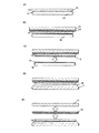
以下に、本発明を用いた代表的な転写方法の手順を、簡略的に図1を用いて説明する。
【0031】
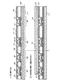
まず図1(A)について説明する。10は基板、11は剥離層、12は酸化物層、13は被剥離体であり、12の酸化物層を含む。
【0032】
基板10はガラス基板、石英基板、セラミックス基板などを用いることができる。また、シリコン基板、金属基板またはステンレス基板を用いても良い。
【0033】
基板10上に窒化物層または金属層からなる剥離層11を形成する。金属層としての代表的な一例は、チタン(Ti)、アルミニウム(Al)、タンタル(Ta)、タングステン(W)、モリブデン(Mo)、銅(Cu)、クロム(Cr)、ネオジム(Nd)、鉄(Fe)、ニッケル(Ni)、コバルト(Co)、ルテニウム(Ru)、ロジウム(Rh)、パラジウム(Pd)、オスミウム(Os)、イリジウム(Ir)から選ばれた元素、または前記元素を主成分とする合金からなる単層、又はこれらの積層構造である。窒化物層としての代表的な一例は、上記金属元素の窒化物、例えば、窒化チタン、窒化タングステン、窒化タンタル、窒化モリブデンからなる単層、またはこれらの積層構造である。
【0034】
次いで、剥離層11である窒化物層または金属層上に、酸化物層12を含む被剥離体13を形成する。酸化物層としては、珪素酸化物、酸化窒化珪素又は金属酸化物を用いた酸化物層を形成すればよい。なお、酸化物層12はスパッタ法、プラズマCVD法、塗布法などのいずれの成膜方法を用いても良い。
【0035】
被剥離体13には、半導体素子(薄膜トランジスタ、有機薄膜トランジスタ、薄膜ダイオード光電変換素子や抵抗素子など)が含まれていてもよい。
【0036】
次に、図1(B)について説明する。被剥離体13上に両面テープ14の一方の面を接着する。両面テープには、紫外線剥離型粘着剤又は熱剥離型粘着剤を用いたものを用いる。この際、剥離体13と両面テープ14との間に気泡が入ると、後の剥離工程の際に被剥離体13にクラックが生じやすくなるため、被剥離体13と両面テープ14との間に気泡が入らないように接着する。なお、この工程にテープマウンター装置等を用いることにより、短時間で剥離体13と両面テープ14との間に気泡が入らないように接着できる。
【0037】
両面テープ14の他方の面に支持体15を接着する。支持体15は、例えば、石英ガラス、金属、セラミックス等であってもよい。この際、支持体15を両面テープ14にしっかり固定する必要がある。これは、被剥離体13を基板10から剥離する際に、支持体15と両面テープ14とが先に剥がれてしまうのを避けるためである。なお、この工程にプレス機等を用いることにより、短時間で支持体に両面テープを接着できる。
【0038】
次に、図1(C)について説明する。窒化物層または金属層からなる剥離層11と酸化物層12とに物理的力を加えることで、被剥離体13から剥離層11を剥離する。ここでは、基板の機械的強度が十分である例を示している。剥離層11と酸化物層12との密着性が高く、かつ基板10の機械的強度が低いと、剥離の際に基板10が割れてしまう恐れがあるので、基板裏面(剥離層が形成されていない面)に支持体(図示しない)、例えばプラスチック、ガラス、金属、セラミックス等を貼りつけた後剥離すると、さらに効果的に剥離することが可能である。
【0039】
なお、物理的力とは、例えば、人間の手、ノズルから吹付けられるガスの風圧、超音波等の比較的小さな力である。
【0040】
次に、図1(D)について説明する。被剥離体を接着剤16を使用して転写体17に接着する。なお、接着剤16は、反応により剥離が可能な粘着剤(以下、反応硬化型接着剤と示す。)、熱により剥離が可能な粘着剤(以下、熱硬化型接着剤と示す。)又は紫外線硬化型接着剤等の光により剥離が可能な粘着剤(以下、光硬化型接着剤と示す。)を用いることが可能であり、それらの代表例として、エポキシ樹脂、アクリル樹脂、シリコーン樹脂等が挙げられる。
【0041】
次に、図1(E)について説明する。被剥離体13と両面テープ14とを剥離する。両面テープ14に紫外線剥離型両面テープを用いた場合、紫外線光を短時間、具体的には50〜100秒照射することで剥離することができる。また、両面テープ14に熱剥離型両面テープを用いた場合、基板を加熱することで剥離することができる。この場合の加熱温度は、90〜150℃、好ましくは110〜120℃と低温であり、加熱時間も2〜3分と短時間である。まずはじめに、支持体15と両面テープ14とを剥離し、その後、被剥離体13と両面テープ14とを剥離する。
【0042】
以上の工程により、転写体上に被剥離体を転写することができる。なお、露出した被剥離体上に、さらに別の基板を貼り合わせてもよい。
【0043】
なお、本明細書中において、転写体とは、被剥離体から基板を剥離した後、被剥離体を接着させるものであり、材料は特に限定されず、プラスチック、ガラス、金属、セラミックス等のいかなる材料でもよい。同様に、支持体とは物理的手段により基板を剥離する際に、被剥離体を接着するものであり、材料は特に限定されずプラスチック、ガラス、金属、セラミックス等のいかなる材料でもよい。
また、転写体及び支持体の形状は特に限定されず、平面を有するもの、曲面を有するもの、可撓性を有するもの、フィルム状のものであっても良い。また、軽量化を最優先するのであれば転写体は、フィルム状のプラスチック、例えば、ポリエチレンテレフタレート(PET)、ポリエーテルスルホン(PES)、ポリエチレンナフタレート(PEN)、ポリカーボネート(PC)、ナイロン、ポリエーテルエーテルケトン(PEEK)、ポリスルホン(PSF)、ポリエーテルイミド(PEI)、ポリアクリレート(PAR)、ポリブチレンテレフタレート(PBT)、極性基のついたノルボルネン樹脂からなるARTON(JSR製)などが好ましい。これらのプラスチックの表面には、窒化アルミニウム、又は窒化酸化アルミニウム等の熱導電性を有する膜を成膜してもよい。また、これらのプラスチック中に鉄、銅、アルミニウム、窒化アルミニウム、又は酸化マグネシウム等を分散させてもよい。これらのプラスチックを転写体に用いると、剥離体にCPU、メモリ等の高速動作を行う半導体回路を設けた場合、駆動により発生した熱を転写体で吸収することが可能である。
【0044】
また、本発明では、浸漬工程がないため、耐水性の弱い部材(転写体に紙、布、木材、金属等)を転写体に用いることができる。また、熱導電性を有する樹脂も用いることができる。 さらには、半導体素子で形成される半導体装置(ロジック回路、メモリー、駆動回路、電源回路、スイッチ等)を転写体とし、この上に、別の半導体装置を転写することも可能である。この場合、各半導体装置の特性を調べ、特性の優れたもの(不良品でないもの)のみ、積層させることができるため、全体の歩留まりが向上するという効果がある。
【0045】
(実施の形態2)
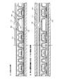
ここでは、本発明の転写工程に用いる剥離可能な粘着媒体(代表例として、両面テープを採用する。)の構造について説明する。
【0046】
図11(A)及び図11(B)を説明する。本発明で用いる両面テープは、第1の粘着剤501を有する第1の基体502と、第2の粘着剤503を有する第2の基体504とを、硬化接着剤505で貼り合わせたものである。第1の粘着剤及び第2の粘着剤には、それぞれ熱剥離型粘着剤及び/又は紫外線剥離型粘着剤を用いることができる。また、紫外線剥離型粘着剤又は熱剥離型粘着剤の変わりに、光(可視光、赤外光等)を照射することによって剥離が可能な粘着剤(光剥離型粘着剤)、化学反応によって剥離が可能な粘着剤(反応剥離型粘着剤)を用いることもできる。
本実施の形態では、粘着剤代表例として熱剥離型粘着剤及び紫外線剥離型粘着剤を用いる。なお、他の粘着剤を用いることも可能である。
【0047】
なお、本実施の形態では、第1の粘着剤501は支持体506に、第2の粘着剤509は被剥離体507にそれぞれ接着するものを表す。
【0048】
図11(B)では、第1の粘着剤508に熱剥離型粘着剤を、第2の粘着剤509に紫外線剥離型粘着剤を用いた例を示したが、この組み合わせに限られるものではなく、図11(C)のように、第1の粘着剤510に紫外線剥離型粘着剤を、第2の粘着剤511に熱剥離型粘着剤を用いることもできる。
【0049】
さらには、第1の粘着剤及び第2の粘着剤に、同一の種類からなる粘着剤を用いても良い。図11(D)では、第1の粘着剤512及び第2の粘着剤513に、熱剥離型粘着剤を用いた例、図11(E)では、第1の粘着剤514及び第2の粘着剤515に紫外線剥離型を用いた両面テープを示す。
【0050】
一方、図11(A)〜図11(E)では、第1の基体502および第2の基体504を張り合わせた両面テープを示したが、図11(F)のように、第1の基体516の両面にそれぞれ熱剥離型粘着剤及び/又は紫外線剥離型粘着剤517、518を有するものでもよい。
【0051】
なお、本実施の形態では、基体の両面に粘着剤を有する剥離可能な粘着媒体を示したが、これに限られず、剥離が可能な粘着剤のみの粘着媒体も本発明に適応することができる。
【0052】
【実施例】
[実施例1]
本発明の実施例を図2〜図6を用いて説明する。ここでは、被剥離体に、薄膜トランジスタを有する積層体の転写方法について説明する。まずはじめに、同一基板上に画素部と、画素部の周辺に設ける駆動回路のTFTを同時に作製する方法について説明する。
【0053】
図2(A)について説明する。基板100に剥離層である窒化物膜又は金属膜101、酸化物層102、下地膜の酸化珪素膜103、非晶質半導体膜104を形成し、その上にニッケルを含む溶液105を塗布する。
【0054】
本実施例では、基板100には、ガラス基板を用いが、特に限定されず、石英基板、半導体基板、金属基板、セラミクス基板等を用いることができる。
【0055】
また、剥離層101において、金属膜を用いるの場合、チタン(Ti)、アルミニウム(Al)、タンタル(Ta)、タングステン(W)、モリブデン(Mo)、銅(Cu)、クロム(Cr)、ネオジム(Nd)、鉄(Fe)、ニッケル(Ni)、コバルト(Co)、ルテニウム(Ru)、ロジウム(Rh)、パラジウム(Pd)、オスミウム(Os)、イリジウム(Ir)から選ばれた元素、または前記元素を主成分とする合金もしくは化合物からなる単層、またはこれらの積層しているものを用いればよい。一方、剥離層101に窒化物膜を用いるの場合、窒化チタン、窒化タングステン、窒化タンタル、窒化モリブデンからなる単層、またはこれらの積層しているものを用いればよい。ここでは、スパッタ法により50nmのタングステン膜を用いる。
【0056】
また、酸化物層102としては、10〜600nm、好ましくは150〜200nmの珪素酸化物又は金属酸化物からなる単層、またはこれらの積層構造を用いれば良い。ここでは、スパッタ法により膜厚200nmの酸化珪素層を用いる。この金属層101と酸化物層102との結合力は、熱処理には強く、膜はがれなどが生じないが、物理的手段で簡単に酸化物層中、酸化物層と金属層又は酸化物層と窒化物層との界面において剥離することができる。
【0057】
また、下地絶縁層103には、プラズマCVD法で、成膜条件を、成膜温度400℃、原料ガスSiH4、N2Oそれぞれの流量を4sccm、800sccmとして成膜する膜厚10〜200nm(好ましくは50nm)の酸化窒化珪素膜(組成比Si=32%、O=27%、N=24%、H=17%)を用いる。
【0058】
この後、プラズマCVD法で成膜温度300℃、成膜ガスSiH4を用いて膜厚25〜80nm、本実施例では54nmの非晶質珪素膜104を成膜する。なお、半導体膜の材料に限定はないが、好ましくはシリコン又はシリコンゲルマニウム(SixGe1−x(X=0.0001〜0.02))合金などを用い、公知の手段(スパッタ法、LPCVD法、またはプラズマCVD法等)により形成すればよい。
【0059】
また、ニッケル溶液105の濃度は適宜調節すればよく、本実施例では、重量換算で10ppmのニッケルを含む酢酸ニッケル塩溶液を用い、スピナーで非晶質半導体膜上に塗布する。塗布に代えて、スパッタ法でニッケル元素をアモルファスシリコン全面に添加する方法を用いてもよい。
【0060】
次に図2(B)について説明する。加熱処理を行うことで非晶質半導体膜を結晶化させる。この加熱処理は、電気炉の熱処理または強光の照射を用いればよい。電気炉内で加熱処理する場合は、500〜650℃で4〜24時間行えばよい。ここでは、脱水素化のための熱処理(500℃、1時間加熱)の後、結晶化のための熱処理(550℃、4時間の加熱)を行って結晶性珪素膜106を得る。
なお、ここでは、炉を用いた加熱処理を用いて非晶質半導体膜の結晶化を行ったが、ランプアニール装置で結晶化を行ってもよい。なお、ここでは、珪素の結晶化を助長する金属元素としてニッケルを用いた結晶化技術を用いたが、ほかの公知の結晶化技術、例えば固相成長法又はレーザー結晶化法を用いても良い。
【0061】
次いで、結晶性半導体膜表面の酸化膜を希フッ酸等で除去した後、結晶性を高めるために結晶粒内に残される欠陥を補修するための第1のレーザー光(XeCl:波長308nm)の照射を、大気中又は酸素雰囲気中で行う。レーザー光には、波長400nm以下のエキシマレーザー光や、YAGレーザーの第2高調波、第3高調波を用いる。いずれにしても、くり返し周波数10〜1000Hz程度のパルスレーザー光を用い、当該レーザー光を光学系にて100〜500mJ/cm2に集光し、90〜95%のオーバーラップ率をもって照射し、シリコン膜表面を走査させればよい。ここでは、繰り替えし周波数30Hz、エネルギー密度393mJ/cm2で第1のレーザー光の照射を大気中で行う。なお、大気中、または酸素雰囲気中で行うため、第1のレーザー光の照射により表面に酸化膜が形成される。この酸化膜を希フッ酸を用いて除去したのち、オゾン水で表面に極めて薄い酸化膜を形成する。
【0062】
次いで、薄膜トランジスタの閾値を制御するために微量な不純物(ボロン又はリン)のドーピングを行う(図示しない)。ここでは、ジボラン(B2H6)を質量分離しないでプラズマ励起したイオンドープ法を用いる。ドーピング条件は、水素で1%に希釈したジボランを流量30sccmでチャンバー内に導入し、加速電圧を15kVとすることで、ドーズ量1×10¹³/cm2程度のボロンを非晶質半導体膜に添加する。
【0063】
次に図2(C)について説明する。オゾン水で非晶質半導体膜の表面を120秒処理して、1〜5nmの酸化膜から成るバリア層107を形成する。
【0064】
次いで、バリア層107上にスパッタ法にてゲッタリングサイトとなるアルゴン元素を含む非晶質珪素膜108を膜厚50nmで形成する。成膜条件は適宜調節すればよいが、本実施例では、スパッタ法を用い、成膜圧力を0.3Pa、アルゴンガスの流量を50sccm、成膜電力を3kW、成膜温度を150℃とする。なお、上記条件での非晶質珪素膜に含まれるアルゴン元素の原子濃度は、3×10²⁰/cm3〜6×1020/cm3、酸素の原子濃度は、1×1019/cm3〜3×1019/cm3である。その後、電気炉内で550℃、4時間の熱処理を行い、金属元素のゲッタリングを行う。
【0065】
次に図2(D)について説明する。バリア層107をエッチングストッパーとして、ゲッタリングサイトであるアルゴン元素を含む非晶質珪素膜108を、NMD3溶液(テトラメチルアンモニウムハイドロオキサイドを0.2〜0.5%含む水溶液)を用いて除去する。この後、希フッ酸を用いてバリア層である酸化膜を除去する。
【0066】
次に図3(A)について説明する。得られた結晶性半導体膜の表面をオゾン水で処理して、極めて薄い酸化膜を形成する(図示せず)。この上に、レジストからなるマスクを形成しパターニングした後、所望の形状に結晶性半導体膜をエッチングして分離された半導体層121〜124を形成する。この後、レジストからなるマスクを除去する。
【0067】
次いで、シリコン膜の表面を洗浄した後、ゲート絶縁膜となる珪素を主成分とする絶縁膜125を形成する。本実施例では、プラズマCVD法により、成膜ガスにSiH4及びN2Oを用い、それぞれのガス流量比を4/800sccmとし、成膜温度400℃で、膜厚115nmの酸化窒化珪素膜を形成する。
【0068】
次いで、ゲート絶縁膜上に膜厚20〜100nmの第1の導電膜と膜厚100〜400nmの第2の導電膜とを積層する。本実施例では、ゲート絶縁膜上に膜厚30nmの窒化タンタル(TaN)膜126を、窒化タンタル(TaN)膜の上に膜厚370nmのタングステン膜(W)127を順次積層する。
【0069】
第1の導電膜及び第2の導電膜を形成する導電性材料としては、タンタル(Ta)、タングステン(W)、チタン(Ti)、モリブデン(Mo)、アルミニウム(Al)、銅(Cu)から選ばれた元素、または前記元素を主成分とする合金もしくは化合物で形成する。また、第1の導電膜及び第2の導電膜として、リン等の不純物をドーピングした多結晶珪素膜に代表される半導体膜や、銀、パラジウム及び銅からなる合金(AgPdCu合金)膜を用いても良い。また、2層構造に限定されず、たとえば、膜厚50nmのタングステン膜、膜厚500nmのアルミニウムとシリコンからなるの合金(Al−Si合金)膜、膜厚30nmの窒化チタン膜を順次積層した3層構造としてもよい。また、3層構造とする場合、第1の導電膜のタングステンに代えて窒化タングステンを用いてもよいし、第2の導電膜のアルミニウムとシリコンの合金に代えてアルミニウムとチタンの合金(Al−Ti合金)膜を用いてもよいし、第3の導電膜の窒化チタン膜に代えてチタン膜を用いてもよい。また、単層構造であってもよい。
【0070】
次に、図3(B)を説明する。フォトリソフラフィ工程による露光工程により、レジストからなるマスク128〜131を形成し、ゲート電極及び配線(図示しない)を形成するための第1のエッチング処理を行う。第1のエッチング処理では、第1及び第2のエッチング条件で行う。エッチングにはICP(Inductively Coupled Plasma:誘導結合型プラズマ)エッチング法を用いるとよい。ICPエッチング法を用い、エッチング条件(コイル型の電極に印加する電力量、基板側の電極に印加する電力量、基板側の電極温度等)を適宜調節することによって、所望のテーパー形状に膜をエッチングすることができる。なお、エッチング用ガスとしては、塩素(Cl2)、塩化ホウ素(BCl3)、四塩化珪素(SiCl4)、四塩化炭素(CCl4)などを代表とする塩素系ガス、または弗化炭素(CF4)、弗化硫黄(SF6)、弗化窒素(NF3)等を代表とするフッ素系ガス、または酸素(O2)を適宜用いることができる。
【0071】
本実施例では、第1のエッチング条件として、エッチング用ガスに弗化炭素(CF4)、塩素(Cl2)と酸素(O2)を用い、それぞれのガス流量比を25/25/10(sccm)とし、1.5Paの圧力でコイル型電極に500WのRF(13.56MHz)電極を投入してプラズマを生成してエッチングを行う。基板側(試料ステージ)にも150WのRF(13.56MHz)電極を投入し、実質的に負の自己バイアス電圧を印加する。なお、基板側の電極面積のサイズは12.5cm×12.5cmであり、コイル型の電極面積サイズ(ここではコイルの設けられた石英円板)は、直径25cmの円板である。この第一のエッチング条件によりタングステン膜をエッチングして第1の導電層の端部をテーパー形状とする。第一のエッチング条件でのタングステン膜に対するエッチング速度は200.39nm/min、窒化タンタルに対するエッチング速度は80.32nm/min、であり窒化タンタルに対するタングステンの選択比は約2.5である。また、この第1のエッチング条件によって、タングステンのテーパー角度は約26°となる。
この後、レジストからなるマスク128〜131を除去せずに第2のエッチング条件に変え、エッチング用ガスに弗化炭素(CF4)と塩素(Cl2)を用い、それぞれのガス流量比を30/30(sccm)とし、1.5Paの圧力でコイル型電極に500WのRF(13.56MHz)電極を投入してプラズマを生成して約15秒程度のエッチングを行う。基板側(試料ステージ)にも10WのRF(13.56MHz)電極を投入し、実施的に負の自己バイアス電圧を印加する。弗化炭素(CF4)と塩素(Cl2)を混合した第2のエッチング条件ではタングステン膜及び窒化タンタルとも同程度にエッチングされる。第2のエッチング条件でのタングステンに対するエッチング速度は58.97nm/min、窒化タンタルに対するエッチング速度は66.43nm/minである。なお、なお、ゲート絶縁膜上に残渣を残すことなくエッチングするためには、10〜20%程度の割合でエッチング時間を増加させるとよい。
【0072】
上記第1のエッチング処理により第一の導電層と第2の導電層からなる第1の形状の導電層132〜135(第1の導電層132a〜135aと第2の導電層132b〜135b)を形成する。ゲート絶縁膜となる絶縁膜125は10〜20nm程度エッチングされ第1の導電層131〜134で覆われない領域が薄くなったゲート絶縁膜136となる。
【0073】
次に図3(C)を説明する。レジストからなるマスク128〜131を除去せずに第2のエッチング処理を行う。ここでは、エッチング用ガスに弗化硫黄(SF6)、塩素(Cl2)と酸素(O2)とを用い、それぞれのガス流量比を24/12/24(sccm)とし、2.0Paの圧力でコイル型の電極に700WのRF(13.56MHz)電極を投入してプラズマを生成してエッチングを25秒行う。基板側(試料ステージ)にも4WのRF(13.56MHz)電力を投入し、実質的に負の自己バイアス電圧を印加する。第2のエッチング処理でのタングステン(W)に対するエッチング速度は227.3nm/minであり、窒化タンタル(TaN)に対するWの選択比は7.1であり、絶縁膜136であるの酸化窒化珪素膜に対するエッチング速度は33.7nm/minであり、の酸化窒化珪素膜に対するWの選択比は6.83である。このようにエッチングガスに弗化硫黄(SF6)を用いた場合、絶縁膜136との選択比が高いので膜減りを抑えることができる。
【0074】
この第2のエッチング処理により第2の導電層137b〜140bを形成する。第2の導電層であるタングステン膜137b〜140bのテーパー角度は約70°となる。一方第1の導電膜は、ほとんどエッチングされず、第1の導電層137a〜140aとなる。また、レジストからなるマスク128〜131は、第2のエッチング処理により、レジストからなるマスク145〜148となる。
【0075】
次に図3(D)について説明する。レジストからなるマスク145〜148を除去した後、第1のドーピング処理を行って、図3(D)の状態を得る。ドーピング処理はイオンドープ法、もしくはイオン注入法で行えば良い。イオンドープ法の条件は、ドーズ量を5×10¹³/cm2とし、加速電圧を50kVとしてとしてリン(P)をドーピングする。n型を付与する不純物元素として、P(リン)の代わりにAs(ヒ素)を用いてもよい。この場合、第1の導電膜131〜134及び第2の導電膜137〜140がn型を付与する不純物元素に対するマスクとなり、自己整合的に第一の不純物領域141〜144が形成される。第1の不純物領域141〜144には1×1016〜1×1017/cm3の濃度範囲でn型を付与する不純物元素を添加する。ここでは、第1の不純物領域と同じ濃度範囲の領域をn―領域とも呼ぶ。
【0076】
なお、本実施例ではレジストからなるマスク145〜148を除去した後、第1のドーピング処理を行ったが、レジストからなるマスク145〜148を除去せずに第1のドーピング処理を行ってもよい。
【0077】
次に図4(A)について説明する。レジストからなるマスク150〜153を形成し第2のドーピング処理を行う。マスク150は駆動回路のpチャネル型TFTを形成する半導体層のチャネル形成領域及びその周辺の領域を保護するマスクであり、マスク151は駆動回路のnチャネル型TFTの一つを形成する半導体層のチャネル形成領域及びその周辺の領域を保護するマスクであり、マスク152及び153は画素領域のTFTを形成する半導体層のチャネル形成領域およびその周辺の領域を保護するマスクである。
【0078】
第2のドーピング処理におけるイオンドープ法の条件を、ドーズ量を3.5×10¹⁵/cm2とし、加速電圧を65kVとしてリン(P)をドーピングして、第2の不純物領域155を形成する。第2の不純物領域155には、1×1020〜1×1021/cm3の濃度範囲でn型を付与する不純物元素を添加している。ここでは、第2の不純物領域と同じ濃度範囲の領域をn+領域とも呼ぶ。
【0079】
次に図4(B)について説明する。レジストからなるマスク150〜153を除去した後、新たにレジストからなるマスク158を形成して、第3のドーピング処理を行う。
【0080】
駆動回路において、第3のドーピング処理により、pチャネル型TFTを形成する半導体層にp型の導電型を付与する不純物元素が添加された第3の不純物領域159〜161及び第4の不純物領域162〜164を形成する。
【0081】
第3の不純物領域159〜161には、1×10²⁰〜1×10²¹/cm3の濃度の範囲でp型を付与する不純物元素が添加されるように不純物元素を添加する。なお、第3の不純物領域159〜161には、先の工程でP(リン)が添加された領域(n―領域)であるが、p型を付与する不純物元素の濃度がその1.5〜3倍添加されているので導電型はp型となる。ここでは、第3の不純物領域と同じ濃度範囲の領域をp+領域とも呼ぶ。
【0082】
また、第4の不純物領域162〜164には、1×10¹⁸〜1×10²⁰/cm3の濃度範囲でp型を付与する不純物元素が添加されるように不純物元素を添加する。ここでは、第4の不純物領域と同じ濃度範囲の領域をp−領域とも呼ぶ。
【0083】
以上までの工程で、それぞれの半導体層にn型又はp型の導電型を有する不純物領域が形成される。導電層137〜140はTFTのゲート電極となる。
【0084】
次に図4(C)を説明する。膜厚100nmの窒化珪素膜からなる第1のパッシベーション膜165を成膜したのち、300〜550℃で1〜12時間加熱し、半導体層を水素化する。本実施例では、窒素雰囲気中で410℃、1時間加熱する。この工程は、第1のパッシベーション膜165に含まれる水素により、半導体層のダングリングボンドを終端する工程である。
【0085】
その後、第1のパッシベーション膜上に無機絶縁物又は有機絶縁物からなる第1の層間絶縁膜166を形成する。有機絶縁物としては、ポジ型感光性有機樹脂又はネガ型感光性有機樹脂を用いることができる。感光性有機樹脂を用いた場合、フォトリソフラフィ工程による露光処理を行い、感光性有機樹脂をエッチングすると192のように曲率を有する第1の開口部を形成することができる。このように曲率を有する開口部を形成することは、後に形成する電極の被覆率(カバレッジ)が高くなるという効果がある。本実施例では、第1の層間絶縁膜に厚さ1.05μmの感光性アクリル樹脂膜を形成する。この後、第1の層間絶縁膜のパターニング及びエッチングを行い、なだらかな内壁を有する第1の開口部を形成する。
なお、ポジ型の感光性樹脂は茶色に着色しているため、第1の層間絶縁膜166にポジ型の感光性有機樹脂を用いる場合、エッチング後に感光性有機樹脂の脱色処理を行う必要がある。
【0086】
また、第1の層間絶縁膜166に無機絶縁物からなる膜を用いた場合、表面を平坦化してもよい。
【0087】
次に、開口部及び第1の層間絶縁膜を覆うように窒化絶縁膜(代表的には、窒化珪素膜又は窒化酸化珪素膜)からなる第2のパッシベーション膜180を形成する。本実施例では第2のパッシベーション膜に窒化珪素膜を用いる。成膜条件としては、高周波放電によるスパッタ法で、シリコンターゲットを用い、スパッタガスとして窒素気体を用いればよい。圧力は適宜設定すれば良いが、0.5〜1.0Pa、放電電力は2.5〜3.5KW、成膜温度は室温(25℃)〜250℃の範囲内であればよい。窒化絶縁膜からなる第2のパッシベーション膜を形成することにより、第1の層間絶縁膜から発生する脱ガスを抑制することができる。
【0088】
第1の層間絶縁膜上に、窒化絶縁膜を形成することにより、基板側から侵入する水分、又は第1の層間絶縁膜から発生する脱ガスが、後に形成されるEL素子に侵入するのを防ぐことができ、EL素子の劣化を抑制することができる。また、この窒化絶縁膜は、後に剥離工程で接着する両面テープを剥がしやすく効果があり、残留した接着材を除去する為の工程を必要としないため、プロセスの簡易化が可能である。
【0089】
次に、フォトリソグラフィ工程による露光処理を行った後、第2のパッシベーション膜180、第1のパッシベーション膜165、ゲート絶縁膜136を順次エッチングし、第2の開口部を形成する。このときの、エッチング処理は、ドライエッチング処理でもウエットエッチング処理でもよい。本実施例では、ドライエッチングにより第2の開口部を形成する。
【0090】
次に、第2の開口部を形成した後、第2のパッシベーション膜上及び第2の開口部に金属膜を形成し、フォトリソグラフィー工程による露光の後、金属膜をエッチングしてソース電極及びドレイン電極181〜188、配線(図示しない)を形成する。金属膜は、アルミニウム(Al)、チタン(Ti)、モリブデン(Mo)、タングステン(W)もしくはシリコン(Si)の元素からなる膜又はこれらの元素を用いた合金膜を用いる。本実施例では、チタン膜/チタンーアルミニウム合金膜/チタン膜(Ti/Al−Si/Ti)をそれぞれ100/350/100nmに積層したのち、所望の形状にパターニング及びエッチングしてソース電極、ドレイン電極及び配線(図示しない)を形成する。
【0091】
その後、画素電極190を形成する。画素電極190には、ITO、SnO2等の透明導電膜を用いることができる。本実施例では、ITOを110nm成膜し、所望の形状にエッチングすることで画素電極190を形成する。
【0092】
なお、本実施例では透過型(下方出射型)表示装置の作製方法を記載しているため画素電極190を透明電極としたが、反射型(上方出射型)表示装置を作製する場合には、画素電極にはアルミニウム(Al)又は銀(Ag)を主成分とする膜、又はそれらの積層構造等の反射性に優れた材料を用いることが望ましい。
【0093】
次に図5(B)について説明する。第2のパッシベーション膜、ソース電極、ドレイン電極、画素電極上に有機絶縁物からなる膜を形成した後、フォトリソグラフィ工程による露光処理を行い、有機絶縁物からなる膜をエッチングし、第3の開口部を形成することで第2の層間絶縁膜間200を形成する。有機絶縁物としては、ポジ型感光性有機樹脂およびネガ型感光性有機樹脂を用いることができる。本実施例では、厚さ1.5μmの感光性アクリル樹脂を用いて第2の層間絶縁膜を形成したのちウエットエッチングする。
【0094】
次に、第2の層間絶縁膜間絶縁膜200上に第3のパッシベーション膜315を形成した後、画素電極190上に第4の開口部を形成する。第3のパッシベーション膜315で第2の層間絶縁膜200を覆うことにより、第2の層間絶縁膜から発生する脱ガスを抑制することができる。第3のパッシベーション膜としては、窒化絶縁膜(代表的には、窒化珪素膜又は窒化酸化珪素膜)からなる膜を用いると効果的である。
【0095】
以上の様にして、pチャネル型TFT195とnチャネル型TFT196からなる駆動回路201、画素TFT197及びpチャネル型TFT198とを有する画素部202を同一基板上に形成することができる。こうして、アクティブマトリクス基板A203が完成する。次に、アクティブマトリクス基板Aから、ガラス基板を剥離してプラスチック基板に転写する工程を示す。
【0096】
次に図6(A)を説明する。第3のパッシベーション膜及び画素電極190に両面テープ210の一方の面を粘着する。この際、第2の層間絶縁膜200及び画素電極190上と両面テープ210の間に気泡が入ると、アクティブマトリクス基板A203から剥離層であるタングステン膜101及びガラス基板を均一に剥離できない恐れがあるため、気泡が入らないように接着する必要がある。本実施例では、一方に紫外線剥離型粘着剤が、他方に熱剥離型粘着剤を有する両面テープを使用し、紫外線剥離型粘着剤を有する面を第3のパッシベーション膜315及び画素電極190に接着する。なお、上記の両面テープの代わりに、両面に紫外線剥離型接着剤を有する両面テープや両面に熱剥離型接着剤を有する両面テープを用いることもできる。
【0097】
次に、両面テープ210の他方の面(熱剥離型粘着剤を有する面)に支持体211を接着する。支持体211は、例えば、石英ガラス、金属、セラミックス等を用いることができる。なお、両面テープ210と支持体211とをしっかりと固定しなければならない。これはアクティブマトリクス基板A203から基板を剥離する際に支持体211と両面テープとが剥がれるのを避けるためである。本実施例では、支持体211に石英ガラスを用いて、両面テープの熱剥離型粘着剤を有する面に石英ガラスを接着する。
【0098】
次に、窒化物層または金属層101と酸化膜からなる層102とに物理的力を加えることで、アクティブマトリクス基板から金属層101及びガラス基板100を剥離する。ガラス基板100を剥離したアクティブマトリクス基板をアクティブマトリクス基板B215と示す。ここでは、ガラス基板100の機械的強度が十分である例を示している。窒化物層または金属層101と酸化膜からなる層102との密着性が高く、ガラス基板100の機械的強度が低い場合、ガラス基板100が割れてしまう可能性があるので、ガラス基板の裏面(TFTが形成されていない面)に支持体(図示しない)、例えばプラスチック、ガラス、金属、セラミックス等を貼りつけた後剥離すると、さらに効果的に剥離が可能である。
【0099】
次に、図6(B)について説明する。酸化膜からなる層102を接着剤212を使用して転写体213に接着する。接着剤212は、反応硬化型接着剤、熱硬化型接着剤又は紫外線硬化型接着剤等の光硬化型接着剤を用いることが可能であり、それらの代表例として、エポキシ樹脂、アクリル樹脂、シリコーン樹脂等が挙げられる。本実施例では、接着剤212に紫外線硬化型接着剤を、転写体213にポリカーボネートフィルムを用いる。接着条件は適宜設定すれば良いが、50〜100℃程度に加熱されたホットプレート上で紫外線を120秒照射してアクティブマトリクス基板にポリカーボネートフィルムを固定する。
【0100】
次に、アクティブマトリクス基板B215から、両面テープ210及び支持体211とを剥離する。まずはじめに、90〜150℃、好ましくは110〜120℃に加熱したのち、両面テープ210から石英ガラス基板211を剥離する。
その後、紫外線を60秒照射して、第2の層間絶縁膜200及び画素電極190から両面テープ210を剥離する。
本実施例では、剥離体側に紫外線剥離型粘着剤を用い、支持体側に熱剥離型粘着剤を有する両面テープを使用したが、この組み合わせに限られるものではなく、剥離体に熱剥離型粘着剤を、支持体に熱剥離型粘着剤を有する両面テープを用いることも可能である。同様に、熱剥離型粘着剤のみを有する両面テープ又は紫外線硬化型粘着剤のみを有する両面テープを用いることも可能である。さらには、光剥離型粘着剤、反応剥離型粘着剤を用いることも可能であり、それぞれの剥離条件を適宜適応すれば良い。
【0101】
以上の工程により、プラスチック基板上に薄膜トランジスタを転写することができる。
【0102】
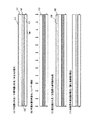
次に、本実施例により転写した薄膜トランジスタの電圧/電流特性を図14に示す。なお、Vds(ソース領域とドレイン領域の電圧差)を1Vとした。
【0103】
まずはじめに、図14(A)について説明する。図14(A)は、Nチャネル型TFTの電気特性を表している。プラスチック基板上に転写したNチャネル型TFTの電気特性は、転写前のTFT、つまりガラス基板上に形成したNチャネル型TFTの電気特性とほとんど変化していないことから、Nチャネル型TFTに欠陥を生じさせることなくプラスチック基板上にTFTを転写していることがわかる。
【0104】
次に、図14(B)について説明する。図14(B)は、Pチャネル型TFTの電気特性を表している。図14(A)と同様に、プラスチック基板上に転写したPチャネル型TFTの電気特性は、転写前のTFT、つまりガラス基板上に形成したPチャネル型TFTの電気特性と変化していないことから、Pチャネル型TFTに欠陥を生じさせることなくプラスチック基板上にTFTを転写していることがわかる。
【0105】
このように、紫外線剥離型粘着剤または熱剥離型粘着剤を有する両面テープを用いることにより、ガラス基板上に形成した薄膜トランジスタを、プラスチック基板上に短時間で転写することが可能であり、しかも、ガラス基板上で作製した薄膜トランジスタと同等の電気特性を有する薄膜トランジスタをプラスチック基板上に作製することができる。
【0106】
また、ガラス基板から薄膜トランジスタを含む剥離体を剥離する際に両面テープを用いることにより、支持体である石英ガラス基板を破損せず剥離することが可能であり、支持体を再度利用することができる。このため、石英ガラスのような高価な材料、希少な材料を支持体に用いる場合、大幅なコストダウンを図ることができる。
【0107】
さらには、被剥離体の表面が露出されているため、プラスチック基板上に転写した後の薄膜トランジスタの電気特性を測定することが可能である。
【0108】
[実施例2]
本実施例では、プラスチック基板上に形成されたEL(Electro Luminescence)素子316を備えたELモジュールを作製する例を説明する。説明には図7を用いる。
【0109】
まず、実施例1に従い、図6(B)のアクティブマトリクス基板C216を作製した後、第3のパッシベーション膜315及び画素電極190上にEL層313を形成する。EL層313は、発光層、電荷注入層、又は電荷輸送層といった薄膜を積層して構成することが一般的である。EL層として一重項励起により発光(蛍光)する発光材料(シングレット化合物)からなる薄膜、または三重項励起により発光(リン光)する発光材料(トリプレット化合物)からなる薄膜を用いることができる。また、EL層313の各層は、有機材料からなる薄膜のみ、又は有機材料からなる薄膜と無機材料からなる薄膜の積層構造でもよい。さらに、有機材料は高分子でも低分子であってもよい。これらの有機材料や無機材料は公知の材料を用いることができる。各層の成膜方法は、公知の手段を用いる。本実施例では、蒸着法により、膜厚20nmのCuPc膜、膜厚30nmのα―NPD膜、膜厚50nmのAlq3膜、膜厚2nmのBaF2膜を積層してEL層313を形成する。
次に、EL層313上に陰極314を成膜し、さらにその上に第4のパッシベーション膜(図示しない)を設ける。陰極314は、周期表の1族又は2族に属する元素を含む金属薄膜を用いればよいが、アルミニウムに0.2〜1.5wt%(好ましくは、0.5〜1.0wt%)のリチウムを添加した金属膜が電荷注入性等により好適である。なお、本発明では、第1〜第4のパッシベーション膜により、リチウム元素が薄膜トランジスタに拡散することを抑制されるため、リチウム元素が薄膜トランジスタの動作に影響を及ぼすことはない。
以上の工程により、画素電極190、EL層313及び陰極314によりEL素子316を形成する。
【0110】
図7(A)に示した構造は下方出射型発光装置であり、EL素子から発した光は画素電極190を透過してプラスチック基板213側から出射される。
【0111】
一方、画素電極190の代わりに反射性を有する金属膜を用い、陰極314に膜厚の薄い(好ましくは、10〜50nm)金属膜を用いることにより、EL素子から発した光は、陰極を透過して出射される。反射性を有する金属膜としては、陽極として機能させるためにPt(白金)又はAu(金)といった仕事関数の高い金属膜を用いる。陰極には、周期表の1族又は2族に属する元素を含む金属膜を用いる。
【0112】
このような上方出射型発光装置では、画素電極の下方を光が透過することがないため、メモリ素子又は抵抗素子を設けること可能であり、第1の層間絶縁膜166が着色されていてもかまわない。このため、設計の自由度が高く、また、製造工程を簡略化することも可能である。
【0113】
次に図7(B)を説明する。第4のパッシベーション膜上に第3の層間絶縁膜を形成する。第3の層間絶縁膜319は、成膜後の表面がより平坦であることが好ましい。なお、第3の層間絶縁膜319は、必ずしも設ける必要ない。
【0114】
次に、接着層317により対向基板318を接着することでEL素子を封止する。対向基板には、PES(ポリエチレンサルファイル)、PC(ポリカーボネート)、PET(ポリエチレンテレフタレート)、もしくはPEN(ポリエチレンナフタレート)等のプラスチックを用いることができる。本実施例ではポリカーボネートフィルムを用いる。なお、画素電極190の代わりに反射性を有する金属膜を用い、陰極314に膜厚の薄い(好ましくは、10〜50nm)金属膜を用いる場合、プラスチック基板は透光性を有する材料であることが必要である。本実施例では、接着層317に、エポキシ樹脂を、対向基板に、ポリカーボネートフィルムを用いる。転写体である基板213と対向基板318に、同一材料からなる基板を用いると、熱膨張係数が等しくなるので温度変化による応力歪みの影響を受けにくくすることができる。
そして、必要があれば転写体213及び対向基板318を所望の形状に分断する。そして、公知の技術を用いてFPC(図示しない)を貼りつける。
【0115】
次に、図15について説明する。図15(A)は、本実施例により作製したELモジュールの上面の写真である。図15(B)は、図15(A)の模式図である。転写体213には、ソース側駆動回路201a、ゲート側駆動回路201b、画素部202が形成されている。また、転写体には、FPC1501が設けられている。また、転写体213と対向基板318とがシール剤により封止されている。図15(A)より、本実施例の工程によりプラスチック基板上作製したELモジュールは、発光していることが分かる。また、ELモジュールの転写体及び対向基板にポリカーボネイトフィルムを用いているため、極めて薄いELモジュールを作製することができる。
【0116】
[実施例3]
実施例1及び実施例2により得られるELモジュールの構成を図8の上面図を用いて説明する。実施例2における転写体213がプラスチック基板900に対応する。
【0117】
図8は、EL素子を備えた発光装置を有するモジュール(以下、ELモジュールと示す。)を示す上面図である。プラスチック基板900(代表的には、プラスチックフィルム基板)に、画素部902、ソース側駆動回路901、及びゲート側駆動回路903を形成する。これらの画素部や駆動回路は、上記実施例に従い作製することができる。
また、918はシール材、919は保護膜であり、画素部および駆動回路部はシール材918で覆われ、そのシール材は保護膜919で覆われている。なお、シール材918としては、できるだけ可視光に対して透明もしくは半透明な材料を用いるのが好ましい。また、シール材918はできるだけ水分や酸素を透過しない材料であることが望ましい。シール材918及び保護膜919で封入することにより、発光素子を外部から完全に遮断することができ、外部から水分や酸素等のEL層の酸化による劣化を促す物質が侵入することを防ぐことができる。加えて、保護膜として熱伝導性を有する膜(AlON膜、AlN膜など)を用いれば駆動させたときに生じる発熱を発散することができ、信頼性の高い発光装置を得ることができる。
さらに、接着材を用いて対向基板(図示せず)で封止されている。対向基板の形状および支持体の形状も特に限定されず、平面を有するもの、曲面を有するもの、可撓性を有するもの、フィルム状のものであってもよい。熱や外力などによる変形に耐えるため対向基板はフィルム基板900と同じ材質のもの、例えばプラスチック基板を用いることが望ましい。
【0118】
また、ここでは図示しないが、用いる金属層(ここでは陰極など)の反射により背景が映り込むことを防ぐために、位相差板(λ/4板)や偏光板からなる円偏光板と呼ばれる円偏光手段を基板900上に設けてもよい。
【0119】
なお、908はソース側駆動回路901及びゲート側駆動回路903に入力される信号を伝送するための配線であり、外部入力端子となるFPC(フレキシブルプリントサーキット)909からビデオ信号やクロック信号を受け取る。また、本実施例の発光装置は、デジタル駆動であってもよく、アナログ駆動であってもよく、ビデオ信号はデジタル信号であってもよいし、アナログ信号であってもよい。なお、ここではFPCしか図示されていないが、このFPCにはプリント配線基盤(PWB)が取り付けられていても良い。本明細書における発光装置には、発光装置本体だけでなく、それにFPCもしくはPWBが取り付けられた状態をも含むものとする。また、これらの画素部や駆動回路と同一基板上に複雑な集積回路(メモリ、CPU、コントローラ、D/Aコンバータ等)を形成することも可能であるが、少ないマスク数での作製は困難である。従って、メモリ、CPU、コントローラ、D/Aコンバータ等を備えたICチップを、COG(chipon glass)方式やTAB(tape automated bonding)方式やワイヤボンディング方法で実装することが好ましい。
以上の工程により、プラスチック基板上に信頼性、電気特性ともに高い薄膜トランジスタを有するELモジュールを作製することができる。また、プラスチック基板にプラスチックフィルムを用いることで、非常に小型で軽量なELモジュールを作製することができる。
【0120】
[実施例4]
本実施例では、プラスチック基板上に形成された液晶モジュールを作製する例を説明する。説明には図9を用いる。
【0121】
まずはじめに、図9(A)を説明する。実施例1に従い図6(B)の状態のアクティブマトリクス基板C216を得た後、基板が耐えうる温度範囲での公知の技術を用いて図6(B)のアクティブマトリクス基板C上に配向膜を形成し、配向膜617を形成しラビング処理を行い、アクティブマトリクス基板D600を作製する。
なお、図9(A)の素子a601、素子b602、素子c603、素子d604は、図6(B)の、pチャネルTFT195、nチャネルTFT196、画素TFT197、pチャネルTFT198それぞれに対応している。なお、アクティブマトリクス基板の表面を平坦化するため、公知の技術を用いて、ソース電極、ドレイン電極605〜612、配線(図示せず)を形成した後、第2の層間絶縁膜を形成し、さらに第2の開口部を形成して接続配線614、画素電極615、616を形成する。
【0122】
次に、対向基板620を用意する。対向基板には、PES(ポリエチレンサルファイル)、PC(ポリカーボネート)、PET(ポリエチレンテレフタレート)、もしくはPEN(ポリエチレンナフタレート)等のプラスチックを用いることができる。この対向基板620には、着色層、遮光層が各画素に対応して配置されたカラーフィルター(図示しない)が設けられている。また、駆動回路の部分にも遮光層(図示しない)を設ける。このカラーフィルターと遮光層とを覆う平坦化膜(図示しない)を設ける。次いで、平坦化膜上に透明電極からなる対向電極621を形成し、対向基板の全面に配向膜622を形成し、ラビング処理を施す。これらの工程は、対向基板が耐えうる温度範囲での公知の技術を用いて行うことができる。
【0123】
次に、画素部と駆動回路が形成されたアクティブマトリクス基板D600と対向基板620とをシール材624で貼り合わせる。シール材にはフィラーが混入されていて、このフィラーによって、2枚の基板を均一な間隔で張り合わせる。
その後、両基板の間に液晶材料623を注入し、封止材(図示せず)によって完全に封止する。液晶材料には、公知の液晶材料を用いれば良い。
【0124】
必要があればアクティブマトリクス基板D600及び対向基板620を所望の形状に分断する。さらに、公知の技術を用いて偏向板(図示しない)等を適宜設ける。さらに、公知の技術を用いてFPC(図示しない)を貼りつける。
なお、液晶表示装置の厚さが一定に保てる構造であれば、プラスチック基板213及び対向基板620にプラスチックフィルムのような可撓性を有するプラスチック基板を用いることができる。
【0125】
このようにして、信頼性、電気特性ともに高いアクティブマトリクス型の液晶モジュールを作製することができる。基板にプラスチックを用いているため、非常に軽量な液晶モジュールを作製することができる。
【0126】
[実施例5]
実施例1及び実施例4により得られる液晶モジュールの構成を図10の上面図を用いて説明する。図9におけるプラスチック基板213がプラスチック基板701に対応する。
【0127】
プラスチック基板701の中央には、画素部704が配置されている。画素部704の上側には、ソース信号線を駆動するためのソース信号線駆動回路702が配置されている。画素部704の左右には、ゲート信号線を駆動するためのゲート信号線駆動回路703が配置されている。本実施例に示した例では、ゲート信号線駆動回路703は画素部に対して左右対称配置としているが、これは片側のみの配置でも良く、液晶モジュールの基板サイズ等を考慮して、設計者が適宜選択すれば良い。ただし、回路の動作信頼性や駆動効率等を考えると、図10に示した左右対称配置が望ましい。
【0128】
各駆動回路への信号の入力は、フレキシブルプリント基板(Flexible Print Circuit:FPC)705から行われる。FPC705は、基板701の所定の場所まで配置された配線に達するように、層間絶縁膜および樹脂膜にコンタクトホールを開口し、接続電極309を形成した後、異方性導電膜等を介して圧着される。
【0129】
駆動回路、画素部の周辺には、基板外周に沿ってシール剤707が塗布され、対向基板706が貼り付けられる。その後、シール剤707が塗布されていない部分より液晶材料が注入され、封止剤708によって密閉される。以上の工程により、液晶モジュールが完成する。
【0130】
また、ここでは全ての駆動回路をプラスチック基板上に形成した例を示したが、駆動回路の一部に数個のICを用いてもよい。
【0131】
このようにして、信頼性、電気特性ともに高く軽量なアクティブマトリクス型の液晶モジュールを作製することができる。
【0132】
[実施例6]
実施例1〜実施例5のようにアクティブマトリクス基板、及びそれを用いた液晶モジュール、又はELモジュールを様々な電子機器の表示部に適用することができる。
【0133】
その様な電子機器としては、ビデオカメラ、デジタルカメラ、プロジェクター、ヘッドマウントディスプレイ(ゴーグル型ディスプレイ)、カーナビゲーション、カーステレオ、パーソナルコンピュータ、携帯情報端末(モバイルコンピュータ、携帯電話または電子書籍等)などが挙げられる。それらの例を図12、及び図13に示す。
【0134】
図12(A)はパーソナルコンピュータであり、本体3001、画像入力部3002、表示部3003、キーボード3004等を含む。本発明を適用することにより、小型で軽量なパーソナルコンピュータを作製することが出来る。
【0135】
図12(B)はビデオカメラであり、本体3101、表示部3102、音声入力部3103、操作スイッチ3104、バッテリー3105、受像部3106等を含む。本発明を適用することで、小型で軽量なビデオカメラを作製することが出来る。
【0136】
図12(C)はモバイルコンピュータ(モービルコンピュータ)であり、本体3201、カメラ部3202、受像部3203、操作スイッチ3204、表示部3205等を含む。本発明を適応することで、小型で軽量なモバイルコンピュータ(モービルコンピュータ)を作製することが出来る。
【0137】
図12(D)はゴーグル型ディスプレイであり、本体3301、表示部3302、アーム部3303等を含む。本発明を適用することで、小型で軽量なゴーグル型ディスプレイを作製することが出来る。
【0138】
図12(E)はプログラムを記録した記録媒体(以下、記録媒体と呼ぶ)を用いるプレーヤーであり、本体3401、表示部3402、スピーカ部3403、記録媒体3404、操作スイッチ3405等を含む。なお、このプレーヤーは記録媒体としてDVD(Digtial Versatile Disc)、CD等を用い、音楽鑑賞や映画鑑賞やゲームやインターネットを行うことができる。
本発明を適用することで、小型で軽量な表示が可能なプレーヤーを作製することが出来る。
【0139】
図12(F)はデジタルカメラであり、本体3501、表示部3502、接眼部3503、操作スイッチ3504、受像部(図示しない)等を含む。本発明を適用することで、小型で軽量なデジタルカメラを作製することが出来る。
【0140】
図13(A)は携帯電話であり、本体3901、音声出力部3902、音声入力部3903、表示部3904、操作スイッチ3905、アンテナ3906等を含む。本発明を適用することで、小型で軽量な携帯電話を作製することが出来る。
【0141】
図13(B)は携帯書籍(電子書籍)であり、本体4001、表示部4002、4003、記憶媒体4004、操作スイッチ4005、アンテナ4006等を含む。本発明を適用することすることで、小型で軽量な携帯書籍を作製することが出来る。
【0142】
図13(C)はディスプレイであり、本体4101、支持台4102、表示部4103等を含む。本発明を適用することすることで、小型で軽量なディスプレイを作製することが出来る
【0143】
以上の様に、本発明の適用範囲は極めて広く、半導体装置を有する電子機器に適用することが可能である。
【0144】
【発明の効果】
本発明の構成を実施することにより、以下に示すような効果を得ることが出来る。
【0145】
積層体の被剥離体を、基板から転写体、特にプラスチック基板上に転写することができる。
【0146】
また、半導体素子(薄膜トランジスタ、有機薄膜トランジスタ、薄膜ダイオード、光電変換素子や抵抗素子など)を有する被剥離体を、転写体、特にプラスチック基板上に短時間で転写することができる。
【0147】
また、被剥離体を基板から剥離し、プラスチック基板上に転写した後の薄膜トランジスタを代表とする様々な半導体素子の特性を測定することが可能である。
【0148】
さらに、被剥離体をプラスチック基板上に転写した後、被剥離体上に用いていた支持体を剥離するため、被剥離体を有するデバイスの厚さが薄くなり、デバイス全体の小型化を図ることができる。デバイスが、下方出射型発光装置、透過型液晶表示装置の場合、発光素子から発する光又はバックライトの透過率を高めることができる。
【0149】
さらに、支持体を破損せずに基板から被剥離体を剥離することが可能であり、支持体を再度利用することができる。このため、石英ガラスのような高価な材料、希少な材料を支持体に用いる場合、大幅なコストダウンを図ることができる。
【図面の簡単な説明】
【図1】実施の形態1の本発明の概念を示す図。
【図2】実施例1のアクティブマトリクス基板の作製工程を示す断面図。
【図3】実施例1のアクティブマトリクス基板の作製工程を示す断面図。
【図4】実施例1のアクティブマトリクス基板の作製工程を示す断面図。
【図5】実施例1のアクティブマトリクス基板の作製工程を示す断面図。
【図6】実施例1のアクティブマトリクス基板の剥離工程及び転写工程を示す断面図。
【図7】実施例2のELモジュールの作製工程を示す断面図。
【図8】実施例3のELモジュールの上面図
【図9】実施例4の液晶モジュールの作製工程を示す断面図。
【図10】実施例5の液晶モジュールの表面図
【図11】実施の形態2の本発明の概念を示す図。
【図12】実施例6の本発明を適応した電子機器を示す図。
【図13】実施例6の本発明を適応した電子機器を示す図。
【図14】実施例1において作製したTFTの電気特性を示す図。
【図15】実施例2において作製したELモジュールを示す写真。[0001]
TECHNICAL FIELD OF THE INVENTION
The present invention relates to a method for transferring a laminate. In addition, the present invention relates to a method for manufacturing a semiconductor element in which an object to be peeled including a semiconductor element is transferred to a base, typically, a semiconductor device having a circuit including a thin film transistor. For example, the present invention relates to an electro-optical device typified by a liquid crystal module and a light emitting device typified by an EL module, and an electronic device equipped with such a device as a component.
[0002]
[Prior art]
In recent years, a technique of forming a thin film transistor using a semiconductor layer (having a thickness of about several to several hundred nm) formed over a substrate having an insulating surface has attracted attention. Thin film transistors are widely applied to electronic devices such as ICs and electro-optical devices, and their development is particularly urgent as switching elements for image display devices.
[0003]
Although various applications using such an image display device are expected, various applications are expected to be particularly used for portable devices, and applications that are lightweight, resistant to impact, and capable of being slightly deformed are expected. ing. At present, glass and quartz are often used for substrates of thin film transistors, but these substrates have a disadvantage that they are easily broken and heavy. Further, since it is difficult to increase the size of a glass substrate or a quartz substrate, it is not suitable as a substrate for a thin film transistor in mass production. For this reason, attempts have been made to form thin film transistors on a lightweight and durable plastic substrate, typically a flexible substrate such as a plastic film.
[0004]
However, since the heat resistance of plastic is low, the maximum temperature of the process of forming a thin film transistor has to be lowered, and as a result, a thin film transistor formed over a relatively heat-resistant substrate such as a glass substrate or a quartz substrate is better. At present, it is impossible to form a thin film transistor having excellent electric characteristics.
[0005]
On the other hand, a separation method for separating an object to be separated, which is present on a substrate through a separation layer, from the substrate has already been proposed. For example, the technology described in
[0006]
Furthermore, in Patent Literature 3, similarly to the techniques described in
[0007]
[Patent Document 1]
JP-A-10-125929 (
[Patent Document 2]
JP-A-10-125931 (pages 6 to 10)
[Patent Document 3]
JP-A-2002-217391 (pages 3 to 6, FIG. 9)
[0008]
[Problems to be solved by the invention]
However, in the methods disclosed in
[0009]
In the above method, when a device is manufactured over the separation layer, when high-temperature heat treatment is performed in the device manufacturing process, hydrogen contained in the separation layer is diffused and reduced, and the separation layer is irradiated with laser light. However, there is a possibility that peeling may not be performed sufficiently.
[0010]
Furthermore, when the substrate is separated from the object to be peeled, the transfer body is fixed to the surface of the object to be peeled using a curable adhesive, so that the surface of the object to be peeled, for example, a thin film transistor, specifically, a wiring or a pixel electrode is exposed. Therefore, it is difficult to measure the characteristics of the object after peeling the substrate. In the case where a liquid crystal display device or a light-emitting device is manufactured using an object having such a structure, a structure in which a plurality of substrates are attached to each other is used, and the thickness of the liquid crystal display device or the light-emitting device is increased. There is also a problem that the size of the device cannot be reduced. Further, the liquid crystal display device has a problem that the light emitted from the backlight cannot be effectively extracted from the backlight, and the light emitting device cannot have the light emitted from the light emitting element.
[0011]
In the invention disclosed in Patent Literature 3, the exfoliated body and the second substrate are bonded with a water-soluble adhesive, but the water-soluble adhesive that is exposed to water is actually exposed to water. Since the area is small, there is a problem that it takes time to peel off the second substrate.
[0012]
In view of this problem, it is possible to shorten the peeling time by shaving a part of the second substrate and exposing the temporary adhesive layer having a larger area. In this case, the second substrate is disposable. In addition, when an expensive or rare material such as quartz glass is used for the second substrate, there is a problem that the cost is high.
[0013]
Further, in this case, when an organic resin is used for the interlayer insulating film of the thin film transistor to be peeled, the volume of the interlayer insulating film expands and deforms because the organic resin easily absorbs moisture, and the wiring of the thin film transistor is peeled off. There is also.
[0014]
The present invention has been made in view of the above problems, and the present invention does not damage the object to be peeled in the laminate, and adheres the object to be peeled from the substrate in a short time to the transfer body. The aim is to provide a method.
[0015]
[Means for Solving the Problems]
The present invention relates to a method for transferring a laminate, comprising forming a release layer and a body to be peeled on a substrate, bonding the body to be peeled and a support through a peelable adhesive medium, After peeling, the object to be peeled is adhered onto the transfer body, and the support and the double-sided tape are peeled from the body to be peeled.
[0016]
The present invention also relates to a method for transferring a laminate, comprising forming a release layer and an object to be peeled on a substrate, bonding the object to be peeled and a support through a peelable adhesive medium, and After the peeled body is peeled off by physical means, the peeled body is adhered to the transfer body, and the support and the double-sided tape are peeled from the peeled body.
[0017]
The present invention also relates to a method for transferring a laminate, comprising forming a release layer and an object to be peeled on a substrate, bonding the object to be peeled and a support through a peelable adhesive medium, and After peeling the peeled body by physical means, the first transfer body is adhered to one of the peeled bodies, the support and the peelable adhesive medium are peeled from the peeled body, and the other of the peeled bodies is peeled off. 2 is adhered to the transfer body.
[0018]
Further, the present invention is a method for manufacturing a semiconductor device, in which a peeled layer including a peeling layer and a semiconductor element is formed over a substrate, and the peeled body and a support are bonded to each other through a peelable adhesive medium, After the release layer and the object to be peeled off, the object to be peeled is bonded to the transfer body, and the adhesive medium that can be peeled off from the support is peeled from the body to be peeled.
[0019]
Further, the present invention is a method for manufacturing a semiconductor device, in which a peeled layer including a peeling layer and a semiconductor element is formed over a substrate, and the peeled body and a support are bonded to each other through a peelable adhesive medium, After the release layer and the object to be peeled are separated by physical means, the object to be peeled is bonded to the transfer body, and the adhesive medium that can be peeled from the support is peeled from the body to be peeled.
[0020]
Further, the present invention is a method for manufacturing a semiconductor device, comprising forming a release layer and a body to be peeled over a substrate, bonding the body to be peeled and a support through a peelable adhesive medium, After peeling the peeled body by physical means, the first transfer body is adhered to one of the peeled bodies, the support and the peelable adhesive medium are peeled from the peeled body, and the other of the peeled bodies is peeled off. The second transfer member is bonded.
[0021]
Further, the semiconductor element is a thin film transistor, an organic thin film transistor, an organic thin film transistor, a thin film diode, a photoelectric conversion element, or a resistance element. As a typical example of the photoelectric conversion element, an element made of a PIN junction of silicon can be given.
[0022]
The object to be peeled has an oxide layer in contact with the peeling layer, typically, a single layer made of a silicon oxide or a metal oxide, or a stacked structure thereof.
[0023]
The release layer is a metal film or a nitride film, which are selected from titanium, aluminum, tantalum, tungsten, molybdenum, copper, chromium, neodymium, iron, nickel, cobalt, ruthenium, rhodium, palladium, osmium, and iridium. A single layer made of a selected element, an alloy material containing the aforementioned element as a main component, or a nitride compound of these elements, or a laminated structure of these.
[0024]
The pressure-sensitive adhesive of the peelable pressure-sensitive adhesive medium is a pressure-sensitive adhesive that can be peeled off by heat (hereinafter, referred to as a heat-peelable pressure-sensitive adhesive) or / and a pressure-sensitive adhesive that can be peeled off by irradiation with ultraviolet light (hereinafter, an ultraviolet-ray peelable adhesive). Adhesive).
[0025]
A typical example of the first transfer body is plastic, typically, a flexible plastic such as a plastic film. Further, a member having low water resistance (such as paper, cloth, wood, metal, or the like as a transfer body) can be used for the first transfer body. Further, a member having thermal conductivity can also be used.
[0026]
A typical example of the second transfer member is plastic, typically, a plastic having flexibility such as a plastic film. Further, a member having low water resistance (such as paper, cloth, wood, metal, or the like as a transfer body) can be used for the first transfer body. Further, a member having thermal conductivity can also be used.
[0027]
As a typical example of the physical means, there is a means of peeling off with a relatively small force such as a human hand, a wind pressure of a gas blown from a nozzle, and an ultrasonic wave.
[0028]
In addition, as a peelable adhesive medium, a tape-like material (double-sided tape) in which an adhesive material is provided on both sides of a substrate, a sheet-like material (double-sided sheet), and a film-like material (double-sided film) ) And the like. Hereinafter, in the embodiments and examples, the present invention will be described using a double-sided tape as a typical example of a peelable adhesive medium, but a double-sided sheet or a double-sided film may be applied to this.
[0029]
BEST MODE FOR CARRYING OUT THE INVENTION
An embodiment of the present invention will be described below.
[0030]
(Embodiment 1)
Hereinafter, the procedure of a typical transfer method using the present invention will be briefly described with reference to FIG.
[0031]
First, FIG. 1A is described.
[0032]
As the
[0033]
A
[0034]
Next, an object to be peeled 13 including the
[0035]
The object to be peeled 13 may include a semiconductor element (a thin film transistor, an organic thin film transistor, a thin film diode photoelectric conversion element, a resistance element, or the like).
[0036]
Next, FIG. 1B will be described. One surface of the double-
[0037]
The
[0038]
Next, FIG. 1C will be described. By applying a physical force to the
[0039]
The physical force is, for example, a relatively small force such as a human hand, a gas pressure blown from a nozzle, an ultrasonic wave, or the like.
[0040]
Next, FIG. 1D is described. The object to be peeled is bonded to the transfer body 17 using an adhesive 16. The adhesive 16 may be a pressure-sensitive adhesive that can be peeled off by a reaction (hereinafter, referred to as a reaction-curable adhesive), a pressure-sensitive adhesive that can be peeled off by heat (hereinafter, referred to as a thermosetting adhesive), or ultraviolet light. An adhesive that can be peeled off by light such as a curable adhesive (hereinafter referred to as a photocurable adhesive) can be used, and typical examples thereof include an epoxy resin, an acrylic resin, and a silicone resin. No.
[0041]
Next, FIG. 1E will be described. The
[0042]
Through the above steps, the object to be peeled can be transferred onto the transfer body. Note that another substrate may be attached to the exposed object to be separated.
[0043]
Note that, in this specification, a transfer body is a substance to which a substrate is peeled from a body to be peeled and then the body to be peeled is bonded. The material is not particularly limited, and any material such as plastic, glass, metal, and ceramics can be used. It may be a material. Similarly, the support is used for bonding the object to be separated when the substrate is separated by physical means, and the material is not particularly limited, and may be any material such as plastic, glass, metal, and ceramics.
The shapes of the transfer body and the support are not particularly limited, and may be those having a flat surface, those having a curved surface, those having flexibility, and those having a film shape. If weight reduction is a top priority, the transfer member may be a film-shaped plastic such as polyethylene terephthalate (PET), polyethersulfone (PES), polyethylene naphthalate (PEN), polycarbonate (PC), nylon, or polystyrene. Preferred are ether ether ketone (PEEK), polysulfone (PSF), polyetherimide (PEI), polyacrylate (PAR), polybutylene terephthalate (PBT), and ARTON (manufactured by JSR) made of norbornene resin having a polar group. On the surface of these plastics, a film having thermal conductivity such as aluminum nitride or aluminum nitride oxide may be formed. Further, iron, copper, aluminum, aluminum nitride, magnesium oxide, or the like may be dispersed in these plastics. When such a plastic is used for a transfer body, heat generated by driving can be absorbed by the transfer body when a semiconductor circuit such as a CPU or a memory that operates at high speed is provided in the peeled body.
[0044]
Further, in the present invention, since there is no immersion step, a member having low water resistance (paper, cloth, wood, metal, or the like for the transfer body) can be used for the transfer body. Further, a resin having thermal conductivity can also be used. Further, a semiconductor device (a logic circuit, a memory, a driving circuit, a power supply circuit, a switch, or the like) formed using a semiconductor element can be used as a transfer body, and another semiconductor device can be transferred thereon. In this case, the characteristics of each semiconductor device are examined, and only those having excellent characteristics (non-defective products) can be laminated, so that the overall yield is improved.
[0045]
(Embodiment 2)
Here, the structure of a peelable adhesive medium (a double-sided tape is used as a representative example) used in the transfer step of the present invention will be described.
[0046]
FIG. 11A and FIG. 11B will be described. The double-sided tape used in the present invention is obtained by laminating a
In this embodiment, a heat-peelable pressure-sensitive adhesive and a UV-peelable pressure-sensitive adhesive are used as typical examples of the pressure-sensitive adhesive. In addition, it is also possible to use another adhesive.
[0047]
Note that in this embodiment mode, the
[0048]
FIG. 11B shows an example in which a heat-peelable pressure-sensitive adhesive is used as the first pressure-
[0049]
Further, the same type of adhesive may be used for the first adhesive and the second adhesive. In FIG. 11D, an example in which a heat-peelable adhesive is used for the
[0050]
On the other hand, FIGS. 11A to 11E show a double-sided tape in which the
[0051]
Note that, in the present embodiment, a peelable adhesive medium having an adhesive on both surfaces of the substrate is shown, but the present invention is not limited to this, and an adhesive medium containing only a peelable adhesive can also be applied to the present invention. .
[0052]
【Example】
[Example 1]
An embodiment of the present invention will be described with reference to FIGS. Here, a method for transferring a stacked body including a thin film transistor to an object to be peeled is described. First, a method for simultaneously manufacturing a pixel portion and a TFT of a driver circuit provided around the pixel portion over the same substrate will be described.
[0053]
FIG. 2A will be described. A nitride film or
[0054]
In this embodiment, a glass substrate is used as the
[0055]
In the case where a metal film is used for the
[0056]
Further, as the
[0057]
The
[0058]
Thereafter, a film forming temperature of 300 ° C. and a film forming gas of SiH are formed by a plasma CVD method. 4 Is used to form an
[0059]
The concentration of the
[0060]
Next, FIG. 2B will be described. By performing the heat treatment, the amorphous semiconductor film is crystallized. For this heat treatment, heat treatment in an electric furnace or irradiation with strong light may be used. When heat treatment is performed in an electric furnace, the heat treatment may be performed at 500 to 650 ° C. for 4 to 24 hours. Here, after the heat treatment for dehydrogenation (heating at 500 ° C. for 1 hour), the heat treatment for crystallization (heating at 550 ° C. for 4 hours) is performed to obtain the
Note that here, the amorphous semiconductor film is crystallized by using a heat treatment in a furnace, but may be crystallized by a lamp annealing apparatus. Note that here, a crystallization technique using nickel as a metal element that promotes crystallization of silicon was used, but other known crystallization techniques, for example, a solid phase growth method or a laser crystallization method may be used. .
[0061]
Next, after removing the oxide film on the surface of the crystalline semiconductor film with diluted hydrofluoric acid or the like, a first laser beam (XeCl: wavelength of 308 nm) for repairing defects left in the crystal grains in order to enhance the crystallinity is used. Irradiation is performed in the air or in an oxygen atmosphere. Excimer laser light having a wavelength of 400 nm or less, or a second or third harmonic of a YAG laser is used as the laser light. In any case, a pulse laser beam having a repetition frequency of about 10 to 1000 Hz is used, and the laser beam is applied to the optical system at 100 to 500 mJ / cm. 2 Then, irradiation is performed with an overlap ratio of 90 to 95% to scan the silicon film surface. Here, the repetition frequency is 30 Hz and the energy density is 393 mJ / cm. 2 Irradiates the first laser light in the atmosphere. Note that an oxide film is formed on the surface by irradiation with the first laser light because the irradiation is performed in the air or in an oxygen atmosphere. After removing this oxide film using diluted hydrofluoric acid, an extremely thin oxide film is formed on the surface with ozone water.
[0062]
Next, a small amount of impurity (boron or phosphorus) is doped to control the threshold value of the thin film transistor (not shown). Here, diborane (B 2 H 6 ) Is performed by an ion doping method in which plasma is excited without mass separation. The doping conditions are as follows: diborane diluted to 1% with hydrogen is introduced into the chamber at a flow rate of 30 sccm, and the acceleration voltage is set to 15 kV, so that the dose amount is 1 × 10 13 / Cm 2 About boron is added to the amorphous semiconductor film.
[0063]
Next, FIG. 2C will be described. The surface of the amorphous semiconductor film is treated with ozone water for 120 seconds to form a barrier layer 107 made of an oxide film having a thickness of 1 to 5 nm.
[0064]
Next, an
[0065]
Next, FIG. 2D will be described. Using the barrier layer 107 as an etching stopper, the
[0066]
Next, FIG. 3A will be described. The surface of the obtained crystalline semiconductor film is treated with ozone water to form an extremely thin oxide film (not shown). After a mask made of a resist is formed thereon and patterned, the crystalline semiconductor film is etched into a desired shape to form separated
[0067]
Next, after cleaning the surface of the silicon film, an insulating
[0068]
Next, a first conductive film with a thickness of 20 to 100 nm and a second conductive film with a thickness of 100 to 400 nm are stacked over the gate insulating film. In this embodiment, a tantalum nitride (TaN)
[0069]
As a conductive material forming the first conductive film and the second conductive film, tantalum (Ta), tungsten (W), titanium (Ti), molybdenum (Mo), aluminum (Al), and copper (Cu) are used. It is formed of a selected element, or an alloy or compound containing the above element as a main component. As the first conductive film and the second conductive film, a semiconductor film typified by a polycrystalline silicon film doped with an impurity such as phosphorus or an alloy (AgPdCu alloy) film of silver, palladium, and copper is used. Is also good. The structure is not limited to the two-layer structure. For example, a 50-nm-thick tungsten film, a 500-nm-thick alloy (Al-Si alloy) film of aluminum and silicon, and a 30-nm-thick titanium nitride film are sequentially stacked. It may have a layer structure. In the case of using a three-layer structure, tungsten of the first conductive film may be replaced with tungsten nitride, and an alloy of aluminum and titanium (Al—) may be used instead of the alloy of aluminum and silicon of the second conductive film. A Ti alloy) film may be used, or a titanium film may be used instead of the titanium nitride film of the third conductive film. Further, it may have a single-layer structure.
[0070]
Next, FIG. 3B will be described. By a photolithography process, masks 128 to 131 made of resist are formed, and a first etching process for forming a gate electrode and a wiring (not shown) is performed. The first etching process is performed under the first and second etching conditions. For the etching, an ICP (Inductively Coupled Plasma) etching method may be used. The film is formed into a desired tapered shape by appropriately adjusting the etching conditions (the amount of power applied to the coil-type electrode, the amount of power applied to the substrate-side electrode, the temperature of the substrate-side electrode, etc.) using the ICP etching method. Can be etched. In addition, as an etching gas, chlorine (Cl 2 ), Boron chloride (BCl 3 ), Silicon tetrachloride (SiCl 4 ), Carbon tetrachloride (CCl 4 ) Or carbon fluoride gas (CF) 4 ), Sulfur fluoride (SF 6 ), Nitrogen fluoride (NF 3 ) Or oxygen (O 2) 2 ) Can be used as appropriate.
[0071]
In this embodiment, as a first etching condition, carbon fluoride (CF) is used as an etching gas. 4 ), Chlorine (Cl 2 ) And oxygen (O 2 ), The gas flow ratio is set to 25/25/10 (sccm), a 500 W RF (13.56 MHz) electrode is supplied to the coil type electrode at a pressure of 1.5 Pa to generate plasma, and etching is performed. Do. A 150 W RF (13.56 MHz) electrode is also applied to the substrate side (sample stage), and a substantially negative self-bias voltage is applied. The size of the electrode area on the substrate side is 12.5 cm × 12.5 cm, and the coil-type electrode area size (a quartz disk provided with a coil here) is a disk having a diameter of 25 cm. The tungsten film is etched under the first etching condition to make the end of the first conductive layer tapered. Under the first etching conditions, the etching rate for the tungsten film is 200.39 nm / min, the etching rate for tantalum nitride is 80.32 nm / min, and the selectivity of tungsten to tantalum nitride is about 2.5. In addition, the taper angle of tungsten is about 26 ° due to the first etching condition.
Thereafter, the second etching condition is changed without removing the resist
[0072]
By the first etching process, the first shape
[0073]
Next, FIG. 3C will be described. The second etching process is performed without removing the resist
[0074]
The second
[0075]
Next, FIG. 3D is described. After removing the resist
[0076]
In the present embodiment, the first doping process is performed after removing the
[0077]
Next, FIG. 4A will be described. Masks 150 to 153 made of resist are formed, and a second doping process is performed. The mask 150 is a mask that protects a channel formation region of a semiconductor layer forming a p-channel TFT of the driver circuit and a peripheral region thereof. A
[0078]
The condition of the ion doping method in the second doping process is set as follows: Fifteen / Cm 2 Then, phosphorus (P) is doped at an acceleration voltage of 65 kV to form a second impurity region 155. In the
[0079]
Next, FIG. 4B will be described. After removing the resist masks 150 to 153, a new resist
[0080]
In the driver circuit,
[0081]
The
[0082]
Further, 1 × 10 4 18 ~ 1 × 10 20 / Cm 3 Is added so that the impurity element imparting p-type is added within the concentration range of. Here, a region having the same concentration range as the fourth impurity region is also referred to as a p-region.
[0083]
Through the above steps, an impurity region having n-type or p-type conductivity is formed in each semiconductor layer. The
[0084]
Next, FIG. 4C will be described. After forming a
[0085]
After that, a first
Note that since the positive photosensitive resin is colored brown, in the case where a positive photosensitive organic resin is used for the first
[0086]
In the case where a film made of an inorganic insulator is used for the first
[0087]
Next, a
[0088]
By forming a nitride insulating film over the first interlayer insulating film, moisture entering from the substrate side or degassing generated from the first interlayer insulating film can enter an EL element to be formed later. This can prevent the EL element from deteriorating. Further, this nitride insulating film has an effect that the double-sided tape to be adhered later in the peeling step is easily peeled off, and a step for removing the remaining adhesive is not required, so that the process can be simplified.
[0089]
Next, after performing an exposure process by a photolithography process, the
[0090]
Next, after forming a second opening, a metal film is formed on the second passivation film and in the second opening, and after exposure by a photolithography process, the metal film is etched to form a source electrode and a drain. The electrodes 181 to 188 and wiring (not shown) are formed. As the metal film, a film made of an element of aluminum (Al), titanium (Ti), molybdenum (Mo), tungsten (W), or silicon (Si), or an alloy film using these elements is used. In this embodiment, after a titanium film / titanium-aluminum alloy film / titanium film (Ti / Al-Si / Ti) are laminated in a thickness of 100/350/100 nm, patterning and etching into a desired shape are performed to form a source electrode and a drain. An electrode and a wiring (not shown) are formed.
[0091]
After that, the
[0092]
In this embodiment, the
[0093]
Next, FIG. 5B will be described. After a film made of an organic insulator is formed over the second passivation film, the source electrode, the drain electrode, and the pixel electrode, an exposure process is performed by a photolithography process, and the film made of the organic insulator is etched. By forming a portion, a second interlayer insulating
[0094]
Next, after a
[0095]
As described above, the driver circuit 201 including the p-channel TFT 195 and the n-channel TFT 196 and the pixel portion 202 including the pixel TFT 197 and the p-channel TFT 198 can be formed over the same substrate. Thus, the active matrix substrate A203 is completed. Next, a step of peeling the glass substrate from the active matrix substrate A and transferring the glass substrate to a plastic substrate will be described.
[0096]
Next, FIG. 6A will be described. One surface of the double-
[0097]
Next, the
[0098]
Next, the
[0099]
Next, FIG. 6B will be described. The
[0100]
Next, the double-
Thereafter, the double-
In the present embodiment, a double-sided tape having an ultraviolet release adhesive on the release body side and a heat release adhesive on the support side was used.However, the present invention is not limited to this combination. It is also possible to use a double-sided tape having a heat-peelable pressure-sensitive adhesive on the support. Similarly, a double-sided tape having only a heat-peelable pressure-sensitive adhesive or a double-sided tape having only an ultraviolet-curable pressure-sensitive adhesive can be used. Further, a light-peelable pressure-sensitive adhesive and a reactive-peelable pressure-sensitive adhesive can be used, and the respective peeling conditions may be appropriately adjusted.
[0101]
Through the above steps, the thin film transistor can be transferred onto the plastic substrate.
[0102]
Next, FIG. 14 shows the voltage / current characteristics of the thin film transistor transferred according to the present embodiment. Note that V ds (Voltage difference between the source region and the drain region) was set to 1V.
[0103]
First, FIG. 14A is described. FIG. 14A shows electric characteristics of an N-channel TFT. The electrical characteristics of the N-channel TFT transferred onto the plastic substrate are almost the same as the electrical characteristics of the TFT before transfer, that is, the electrical characteristics of the N-channel TFT formed on the glass substrate. It can be seen that the TFT was transferred onto the plastic substrate without causing any occurrence.
[0104]
Next, FIG. 14B is described. FIG. 14B shows electric characteristics of a P-channel TFT. As in FIG. 14A, the electrical characteristics of the P-channel TFT transferred onto the plastic substrate are not changed from the electrical characteristics of the TFT before transfer, that is, the P-channel TFT formed on the glass substrate. It can be seen that the TFT was transferred onto the plastic substrate without causing any defect in the P-channel TFT.
[0105]
As described above, by using a double-sided tape having an ultraviolet release adhesive or a heat release adhesive, a thin film transistor formed on a glass substrate can be transferred onto a plastic substrate in a short time, and A thin film transistor having the same electric characteristics as a thin film transistor manufactured over a glass substrate can be manufactured over a plastic substrate.
[0106]
In addition, by using a double-sided tape when peeling a peeling body including a thin film transistor from a glass substrate, the quartz glass substrate as a support can be peeled without being damaged, and the support can be reused. . For this reason, when an expensive material such as quartz glass or a rare material is used for the support, a significant cost reduction can be achieved.
[0107]
Further, since the surface of the object to be peeled is exposed, the electrical characteristics of the thin film transistor after being transferred onto the plastic substrate can be measured.
[0108]
[Example 2]
In this embodiment, an example of manufacturing an EL module including an EL (Electro Luminescence)
[0109]
First, according to the first embodiment, after the active matrix substrate C216 in FIG. 6B is manufactured, an
Next, a
Through the above steps, the
[0110]
The structure shown in FIG. 7A is a downward emission type light-emitting device, in which light emitted from an EL element passes through the
[0111]
On the other hand, by using a reflective metal film in place of the
[0112]
In such an upward emission light-emitting device, since light does not pass below the pixel electrode, a memory element or a resistor element can be provided, and the first
[0113]
Next, FIG. 7B will be described. Forming a third interlayer insulating film on the fourth passivation film; It is preferable that the surface of the third
[0114]
Next, the EL element is sealed by bonding the
Then, if necessary, the
[0115]
Next, FIG. 15 will be described. FIG. 15A is a photograph of the top surface of the EL module manufactured according to this example. FIG. 15B is a schematic diagram of FIG. On the
[0116]
[Example 3]
The configuration of the EL module obtained by
[0117]
FIG. 8 is a top view illustrating a module including a light-emitting device including an EL element (hereinafter, referred to as an EL module). A pixel portion 902, a source side driver circuit 901, and a gate side driver circuit 903 are formed over a plastic substrate 900 (typically, a plastic film substrate). These pixel portions and driving circuits can be manufactured according to the above embodiment.
Reference numeral 918 denotes a sealant, and 919 denotes a protective film. The pixel portion and the driver circuit portion are covered with a sealant 918, and the sealant is covered with a protective film 919. Note that as the sealant 918, a material that is as transparent or translucent as possible to visible light is preferably used. It is preferable that the sealant 918 be a material that does not transmit moisture or oxygen as much as possible. By enclosing the light-emitting element with the sealant 918 and the protective film 919, the light-emitting element can be completely shut off from the outside and a substance such as moisture or oxygen, which promotes deterioration of the EL layer due to oxidation, can be prevented from entering. it can. In addition, when a film having thermal conductivity (such as an AlON film or an AlN film) is used as the protective film, heat generated when the device is driven can be radiated, and a highly reliable light-emitting device can be obtained.
Furthermore, it is sealed with a counter substrate (not shown) using an adhesive. The shape of the counter substrate and the shape of the support are also not particularly limited, and may be a flat substrate, a curved substrate, a flexible substrate, or a film substrate. In order to withstand deformation due to heat, external force, or the like, it is desirable to use a counter substrate made of the same material as the film substrate 900, for example, a plastic substrate.
[0118]
Although not shown here, in order to prevent the background from being reflected by the reflection of the metal layer used (eg, a cathode), a circularly polarized light called a circularly polarizing plate including a retardation plate (λ / 4 plate) or a polarizing plate is used. The means may be provided over the substrate 900.
[0119]
Note that reference numeral 908 denotes wiring for transmitting signals input to the source driver circuit 901 and the gate driver circuit 903, and receives a video signal and a clock signal from an FPC (flexible print circuit) 909 serving as an external input terminal. Further, the light emitting device of this embodiment may be driven digitally or analogly, and the video signal may be a digital signal or an analog signal. Although only the FPC is shown here, a printed wiring board (PWB) may be attached to the FPC. The light-emitting device in this specification includes not only the light-emitting device body but also a state in which an FPC or a PWB is attached thereto. Although a complicated integrated circuit (memory, CPU, controller, D / A converter, or the like) can be formed over the same substrate as the pixel portion and the driver circuit, manufacturing with a small number of masks is difficult. is there. Therefore, it is preferable to mount an IC chip including a memory, a CPU, a controller, a D / A converter, and the like by a COG (chipon glass) method, a TAB (tape automated bonding) method, or a wire bonding method.
Through the above steps, an EL module including a thin film transistor with high reliability and electric characteristics over a plastic substrate can be manufactured. Further, by using a plastic film for a plastic substrate, a very small and lightweight EL module can be manufactured.
[0120]
[Example 4]
In this embodiment, an example of manufacturing a liquid crystal module formed over a plastic substrate will be described. FIG. 9 is used for the description.
[0121]
First, FIG. 9A will be described. After obtaining the active matrix substrate C216 in the state of FIG. 6B according to the first embodiment, an alignment film is formed on the active matrix substrate C of FIG. 6B using a known technique in a temperature range that the substrate can withstand. Then, an
Note that the element a 601, the
[0122]
Next, a
[0123]
Next, the active matrix substrate D600 on which the pixel portion and the driver circuit are formed and the
Thereafter, a
[0124]
If necessary, the active matrix substrate D600 and the
Note that as long as the thickness of the liquid crystal display device can be kept constant, a flexible plastic substrate such as a plastic film can be used for the
[0125]
In this manner, an active matrix liquid crystal module having high reliability and high electrical characteristics can be manufactured. Since plastic is used for the substrate, a very lightweight liquid crystal module can be manufactured.
[0126]
[Example 5]
The configuration of the liquid crystal module obtained in
[0127]
At the center of the plastic substrate 701, a pixel portion 704 is arranged. A source signal line driver circuit 702 for driving a source signal line is provided above the pixel portion 704. On the left and right of the pixel portion 704, gate signal line driving circuits 703 for driving gate signal lines are arranged. In the example shown in this embodiment, the gate signal line driving circuit 703 is arranged symmetrically with respect to the pixel portion. However, this may be arranged on only one side. May be appropriately selected. However, considering the operation reliability and driving efficiency of the circuit, the symmetrical arrangement shown in FIG. 10 is desirable.
[0128]
Input of a signal to each drive circuit is performed from a flexible printed circuit (Flexible Print Circuit: FPC) 705. The
[0129]
A
[0130]
Although an example in which all the driving circuits are formed on a plastic substrate is shown here, several ICs may be used as a part of the driving circuit.
[0131]
In this manner, an active matrix type liquid crystal module which has high reliability and electric characteristics and is lightweight can be manufactured.
[0132]
[Example 6]
As in
[0133]
Such electronic devices include video cameras, digital cameras, projectors, head-mounted displays (goggle-type displays), car navigation systems, car stereos, personal computers, personal digital assistants (mobile computers, mobile phones, e-books, etc.). No. Examples thereof are shown in FIGS.
[0134]
FIG. 12A illustrates a personal computer, which includes a
[0135]
FIG. 12B illustrates a video camera, which includes a main body 3101, a display portion 3102, an
[0136]
FIG. 12C illustrates a mobile computer (mobile computer), which includes a main body 3201, a camera portion 3202, an
[0137]
FIG. 12D illustrates a goggle-type display, which includes a
[0138]
FIG. 12E illustrates a player using a recording medium on which a program is recorded (hereinafter, referred to as a recording medium), which includes a main body 3401, a display portion 3402, a
By applying the present invention, a player capable of displaying a small and lightweight display can be manufactured.
[0139]
FIG. 12F illustrates a digital camera, which includes a
[0140]
FIG. 13A illustrates a mobile phone, which includes a
[0141]
FIG. 13B illustrates a portable book (e-book) including a
[0142]
FIG. 13C illustrates a display, which includes a
[0143]
As described above, the applicable range of the present invention is extremely wide, and the present invention can be applied to electronic devices including a semiconductor device.
[0144]
【The invention's effect】
By implementing the configuration of the present invention, the following effects can be obtained.
[0145]
The object to be peeled from the laminate can be transferred from the substrate to a transfer member, particularly a plastic substrate.
[0146]
Further, an object to be peeled including a semiconductor element (a thin film transistor, an organic thin film transistor, a thin film diode, a photoelectric conversion element, a resistance element, or the like) can be transferred onto a transfer body, particularly, a plastic substrate in a short time.
[0147]
In addition, characteristics of various semiconductor elements typified by a thin film transistor after the object to be separated is separated from the substrate and transferred onto a plastic substrate can be measured.
[0148]
Furthermore, after transferring the object to be peeled onto a plastic substrate, the support used on the object to be peeled is peeled off, so that the thickness of the device having the object to be peeled is reduced, and the entire device is reduced in size. Can be. When the device is a downward emission type light emitting device or a transmission type liquid crystal display device, the transmittance of light emitted from the light emitting element or the backlight can be increased.
[0149]
Further, the object to be peeled can be separated from the substrate without damaging the support, and the support can be reused. For this reason, when an expensive material such as quartz glass or a rare material is used for the support, a significant cost reduction can be achieved.
[Brief description of the drawings]
FIG. 1 is a diagram showing the concept of the present invention in
FIG. 2 is a cross-sectional view illustrating a manufacturing process of the active matrix substrate of Example 1.
FIG. 3 is a cross-sectional view illustrating a manufacturing process of the active matrix substrate of Example 1.
FIG. 4 is a cross-sectional view illustrating a manufacturing process of the active matrix substrate of Example 1.
FIG. 5 is a cross-sectional view illustrating a manufacturing process of the active matrix substrate of Example 1.
FIG. 6 is a cross-sectional view illustrating a separation step and a transfer step of the active matrix substrate according to the first embodiment.
FIG. 7 is a cross-sectional view illustrating a manufacturing process of an EL module of Example 2.
FIG. 8 is a top view of an EL module according to a third embodiment.
FIG. 9 is a cross-sectional view illustrating a step of manufacturing the liquid crystal module of Example 4.
FIG. 10 is a front view of a liquid crystal module according to a fifth embodiment.
FIG. 11 is a diagram showing the concept of the present invention in the second embodiment.
FIG. 12 is a diagram showing an electronic apparatus to which the present invention according to a sixth embodiment is applied.
FIG. 13 is a diagram showing an electronic apparatus to which the present invention according to a sixth embodiment is applied.
FIG. 14 is a diagram showing electric characteristics of a TFT manufactured in Example 1.
FIG. 15 is a photograph showing an EL module manufactured in Example 2.
Claims (37)
前記被剥離体に剥離可能な粘着媒体を介して支持体を接着し、
前記剥離層及び前記被剥離体を物理的手段によって剥離した後、前記被剥離体を第1の転写体に接着し、
前記被剥離体から前記支持体及び前記剥離可能な粘着媒体を剥離することを特徴とする積層体の転写方法。Forming an object to be separated on the first substrate with a separation layer interposed therebetween;
Adhering a support via a peelable adhesive medium to the object to be peeled,
After peeling the release layer and the body to be peeled by physical means, the body to be peeled is bonded to a first transfer body,
A method of transferring a laminated body, comprising separating the support and the peelable adhesive medium from the object to be separated.
前記被剥離体に剥離可能な粘着媒体を介して支持体を接着し、
前記剥離層及び前記被剥離体を物理的手段によって剥離した後、前記被剥離体の一方に第1の転写体を接着し、
前記被剥離体から前記支持体及び前記剥離可能な粘着媒体を剥離した後、前記被剥離体の他方に第2の転写体を接着することを特徴とする積層体の転写方法。Forming an object to be separated on the first substrate with a separation layer interposed therebetween;
Adhering a support via a peelable adhesive medium to the object to be peeled,
After peeling the release layer and the body to be peeled by physical means, a first transfer body is bonded to one of the bodies to be peeled,
A method of transferring a laminated body, comprising: after peeling off the support and the peelable adhesive medium from the body to be peeled, bonding a second transfer body to the other of the body to be peeled.
前記被剥離体に剥離可能な粘着媒体を介して支持体を接着し、
前記剥離層及び前記被剥離体を剥離した後、前記被剥離体を第1の転写体に接着し、
前記被剥離体から前記支持体及び前記剥離可能な粘着媒体を剥離することを特徴とする半導体装置の作製方法。Forming an object to be separated having a semiconductor element over a separation layer on a first substrate;
Adhering a support via a peelable adhesive medium to the object to be peeled,
After peeling the release layer and the body to be peeled, the body to be peeled is bonded to a first transfer body,
A method for manufacturing a semiconductor device, wherein the support and the peelable adhesive medium are separated from the object.
前記被剥離体に剥離可能な粘着媒体を介して支持体を接着し、
前記剥離層及び前記被剥離体を物理的手段によって剥離した後、前記被剥離体を第1の転写体に接着し、
前記被剥離体から前記支持体及び前記剥離可能な粘着媒体を剥離することを特徴とする半導体装置の作製方法。Forming an object to be separated having a semiconductor element over a separation layer on a first substrate;
Adhering a support via a peelable adhesive medium to the object to be peeled,
After peeling the release layer and the body to be peeled by physical means, the body to be peeled is bonded to a first transfer body,
A method for manufacturing a semiconductor device, wherein the support and the peelable adhesive medium are separated from the object.
前記被剥離体に剥離可能な粘着媒体を介して支持体を接着し、
前記剥離層及び前記被剥離体を物理的手段によって剥離した後、前記被剥離体の一方に第1の転写体を接着し、
前記被剥離体から前記支持体と前記剥離可能な粘着媒体を剥離した後、前記被剥離体の他方を第2の転写体に接着することを特徴とする半導体装置の作製方法。Forming an object to be separated having a semiconductor element over a separation layer on a first substrate;
Adhering a support via a peelable adhesive medium to the object to be peeled,
After peeling the release layer and the body to be peeled by physical means, a first transfer body is bonded to one of the bodies to be peeled,
A method for manufacturing a semiconductor device, comprising: after peeling the support and the peelable adhesive medium from the body to be peeled, bonding the other of the body to be peeled to a second transfer body.
Priority Applications (1)
| Application Number | Priority Date | Filing Date | Title |
|---|---|---|---|
| JP2003137073A JP2004047975A (en) | 2002-05-17 | 2003-05-15 | Method of transferring laminate and method of manufacturing semiconductor device |
Applications Claiming Priority (2)
| Application Number | Priority Date | Filing Date | Title |
|---|---|---|---|
| JP2002143797 | 2002-05-17 | ||
| JP2003137073A JP2004047975A (en) | 2002-05-17 | 2003-05-15 | Method of transferring laminate and method of manufacturing semiconductor device |
Related Child Applications (2)
| Application Number | Title | Priority Date | Filing Date |
|---|---|---|---|
| JP2004265298A Division JP4757469B2 (en) | 2002-05-17 | 2004-09-13 | Method for manufacturing semiconductor device |
| JP2009092389A Division JP5094776B2 (en) | 2002-05-17 | 2009-04-06 | Method for manufacturing semiconductor device |
Publications (2)
| Publication Number | Publication Date |
|---|---|
| JP2004047975A true JP2004047975A (en) | 2004-02-12 |
| JP2004047975A5 JP2004047975A5 (en) | 2005-06-16 |
Family
ID=31719506
Family Applications (1)
| Application Number | Title | Priority Date | Filing Date |
|---|---|---|---|
| JP2003137073A Withdrawn JP2004047975A (en) | 2002-05-17 | 2003-05-15 | Method of transferring laminate and method of manufacturing semiconductor device |
Country Status (1)
| Country | Link |
|---|---|
| JP (1) | JP2004047975A (en) |
Cited By (21)
| Publication number | Priority date | Publication date | Assignee | Title |
|---|---|---|---|---|
| JP2005311295A (en) * | 2004-03-26 | 2005-11-04 | Semiconductor Energy Lab Co Ltd | Semiconductor device |
| JP2006013462A (en) * | 2004-05-21 | 2006-01-12 | Semiconductor Energy Lab Co Ltd | Semiconductor device and its manufacturing method |
| JP2006032927A (en) * | 2004-06-14 | 2006-02-02 | Semiconductor Energy Lab Co Ltd | Semiconductor device and communication system |
| JP2009503878A (en) * | 2005-08-05 | 2009-01-29 | オスラム オプト セミコンダクターズ ゲゼルシャフト ミット ベシュレンクテル ハフツング | Method for manufacturing a semiconductor component and thin film semiconductor component |
| WO2010026938A1 (en) * | 2008-09-08 | 2010-03-11 | 電気化学工業株式会社 | Semiconductor product manufacturing method |
| KR100987917B1 (en) * | 2006-09-29 | 2010-10-18 | 가부시키가이샤 한도오따이 에네루기 켄큐쇼 | Method for manufacturing semiconductor device |
| US8058083B2 (en) | 2008-11-20 | 2011-11-15 | Semiconductor Energy Laboratory Co., Ltd. | Method for manufacturing flexible semiconductor device |
| US8258512B2 (en) | 2004-05-21 | 2012-09-04 | Semiconductor Energy Laboratory Co., Ltd. | Semiconductor device and manufacturing method thereof |
| JP2013004632A (en) * | 2011-06-14 | 2013-01-07 | Canon Components Inc | Method for manufacturing semiconductor device |
| KR101255301B1 (en) * | 2006-02-13 | 2013-04-15 | 엘지디스플레이 주식회사 | Method for Manufacturing Flexible Display |
| JP5200538B2 (en) * | 2005-08-09 | 2013-06-05 | 旭硝子株式会社 | Thin glass laminate and method for manufacturing display device using thin glass laminate |
| KR101470806B1 (en) * | 2007-02-02 | 2014-12-09 | 가부시키가이샤 한도오따이 에네루기 켄큐쇼 | Method of manufacturing semiconductor device |
| JP2015098565A (en) * | 2013-11-20 | 2015-05-28 | 東京応化工業株式会社 | Processing method |
| US9142720B2 (en) | 2007-01-29 | 2015-09-22 | Osram Opto Semiconductors Gmbh | Thin-film light emitting diode chip and method for producing a thin-film light emitting diode chip |
| US9384439B2 (en) | 2004-06-14 | 2016-07-05 | Semiconductor Energy Laboratory Co., Ltd. | Semiconductor device and communication system |
| WO2016111197A1 (en) * | 2015-01-06 | 2016-07-14 | シャープ株式会社 | Manufacturing method for element substrate |
| JP2018195843A (en) * | 2007-12-03 | 2018-12-06 | 株式会社半導体エネルギー研究所 | Semiconductor device |
| WO2019013212A1 (en) * | 2017-07-14 | 2019-01-17 | 信越化学工業株式会社 | Highly heat conductive device substrate and method for producing same |
| JP2019049754A (en) * | 2009-09-16 | 2019-03-28 | 株式会社半導体エネルギー研究所 | Method for manufacturing electronic apparatus |
| WO2022024655A1 (en) * | 2020-07-31 | 2022-02-03 | 東レ株式会社 | Method for manufacturing laminate |
| US11997859B2 (en) | 2009-09-16 | 2024-05-28 | Semiconductor Energy Laboratory Co., Ltd. | Light-emitting device and manufacturing method thereof |
Families Citing this family (1)
| Publication number | Priority date | Publication date | Assignee | Title |
|---|---|---|---|---|
| DE102007004303A1 (en) | 2006-08-04 | 2008-02-07 | Osram Opto Semiconductors Gmbh | Thin-film semiconductor device and device composite |
Citations (10)
| Publication number | Priority date | Publication date | Assignee | Title |
|---|---|---|---|---|
| JPH06504139A (en) * | 1990-12-31 | 1994-05-12 | コピン・コーポレーシヨン | Single crystal silicon array element for display panels |
| JPH1095189A (en) * | 1997-07-28 | 1998-04-14 | Hitachi Ltd | Manufacture of semiconductor device |
| JPH10125929A (en) * | 1996-08-27 | 1998-05-15 | Seiko Epson Corp | Separation method |
| JPH10125931A (en) * | 1996-08-27 | 1998-05-15 | Seiko Epson Corp | Transfer of thin film element, thin film element, thin film integrated circuit device, active materix substrate and liquid crystal display device |
| JPH10150007A (en) * | 1996-11-18 | 1998-06-02 | Toyo Chem Co Ltd | Semiconductor wafer fixing sheet |
| JPH11142878A (en) * | 1997-11-12 | 1999-05-28 | Sharp Corp | Formation of display transistor array panel |
| JP2001051296A (en) * | 1999-08-06 | 2001-02-23 | Seiko Epson Corp | Production of thin-film device, the thin-film device, production of active matrix substrate, the active matrix substrate and optoelectronic device |
| JP2001057432A (en) * | 1999-08-18 | 2001-02-27 | Seiko Epson Corp | Method for transferring thin film element |
| JP2001189460A (en) * | 1999-12-28 | 2001-07-10 | Seiko Epson Corp | Method of transferring and manufacturing thin-film device |
| JP2002217391A (en) * | 2001-01-23 | 2002-08-02 | Seiko Epson Corp | Method for manufacturing laminate and semiconductor device |
-
2003
- 2003-05-15 JP JP2003137073A patent/JP2004047975A/en not_active Withdrawn
Patent Citations (10)
| Publication number | Priority date | Publication date | Assignee | Title |
|---|---|---|---|---|
| JPH06504139A (en) * | 1990-12-31 | 1994-05-12 | コピン・コーポレーシヨン | Single crystal silicon array element for display panels |
| JPH10125929A (en) * | 1996-08-27 | 1998-05-15 | Seiko Epson Corp | Separation method |
| JPH10125931A (en) * | 1996-08-27 | 1998-05-15 | Seiko Epson Corp | Transfer of thin film element, thin film element, thin film integrated circuit device, active materix substrate and liquid crystal display device |
| JPH10150007A (en) * | 1996-11-18 | 1998-06-02 | Toyo Chem Co Ltd | Semiconductor wafer fixing sheet |
| JPH1095189A (en) * | 1997-07-28 | 1998-04-14 | Hitachi Ltd | Manufacture of semiconductor device |
| JPH11142878A (en) * | 1997-11-12 | 1999-05-28 | Sharp Corp | Formation of display transistor array panel |
| JP2001051296A (en) * | 1999-08-06 | 2001-02-23 | Seiko Epson Corp | Production of thin-film device, the thin-film device, production of active matrix substrate, the active matrix substrate and optoelectronic device |
| JP2001057432A (en) * | 1999-08-18 | 2001-02-27 | Seiko Epson Corp | Method for transferring thin film element |
| JP2001189460A (en) * | 1999-12-28 | 2001-07-10 | Seiko Epson Corp | Method of transferring and manufacturing thin-film device |
| JP2002217391A (en) * | 2001-01-23 | 2002-08-02 | Seiko Epson Corp | Method for manufacturing laminate and semiconductor device |
Cited By (40)
| Publication number | Priority date | Publication date | Assignee | Title |
|---|---|---|---|---|
| JP2005311295A (en) * | 2004-03-26 | 2005-11-04 | Semiconductor Energy Lab Co Ltd | Semiconductor device |
| JP2006013462A (en) * | 2004-05-21 | 2006-01-12 | Semiconductor Energy Lab Co Ltd | Semiconductor device and its manufacturing method |
| US8258512B2 (en) | 2004-05-21 | 2012-09-04 | Semiconductor Energy Laboratory Co., Ltd. | Semiconductor device and manufacturing method thereof |
| JP2006032927A (en) * | 2004-06-14 | 2006-02-02 | Semiconductor Energy Lab Co Ltd | Semiconductor device and communication system |
| US10411037B2 (en) | 2004-06-14 | 2019-09-10 | Semiconductor Energy Laboratory Co., Ltd. | Semiconductor device and communication system |
| US9384439B2 (en) | 2004-06-14 | 2016-07-05 | Semiconductor Energy Laboratory Co., Ltd. | Semiconductor device and communication system |
| JP2009503878A (en) * | 2005-08-05 | 2009-01-29 | オスラム オプト セミコンダクターズ ゲゼルシャフト ミット ベシュレンクテル ハフツング | Method for manufacturing a semiconductor component and thin film semiconductor component |
| JP5200538B2 (en) * | 2005-08-09 | 2013-06-05 | 旭硝子株式会社 | Thin glass laminate and method for manufacturing display device using thin glass laminate |
| KR101255301B1 (en) * | 2006-02-13 | 2013-04-15 | 엘지디스플레이 주식회사 | Method for Manufacturing Flexible Display |
| US8048777B2 (en) | 2006-09-29 | 2011-11-01 | Semiconductor Energy Laboratory Co., Ltd. | Method for manufacturing semiconductor device |
| KR100987917B1 (en) * | 2006-09-29 | 2010-10-18 | 가부시키가이샤 한도오따이 에네루기 켄큐쇼 | Method for manufacturing semiconductor device |
| US9472429B2 (en) | 2006-09-29 | 2016-10-18 | Semiconductor Energy Laboratory Co., Ltd. | Method for manufacturing semiconductor device |
| US8048770B2 (en) | 2006-09-29 | 2011-11-01 | Semiconductor Energy Laboratory Co., Ltd. | Method for manufacturing semiconductor device |
| KR101154834B1 (en) * | 2006-09-29 | 2012-06-18 | 가부시키가이샤 한도오따이 에네루기 켄큐쇼 | Method for manufacturing semiconductor device |
| US8043936B2 (en) | 2006-09-29 | 2011-10-25 | Semiconductor Energy Laboratory Co., Ltd. | Method for manufacturing semiconductor device |
| US9054141B2 (en) | 2006-09-29 | 2015-06-09 | Semiconductor Energy Laboratory Co., Ltd. | Method for manufacturing semiconductor device |
| KR101021051B1 (en) * | 2006-09-29 | 2011-03-15 | 가부시키가이샤 한도오따이 에네루기 켄큐쇼 | Method for manufacturing a semiconductor device |
| KR100987918B1 (en) * | 2006-09-29 | 2010-10-18 | 가부시키가이샤 한도오따이 에네루기 켄큐쇼 | Method for manufacturing semiconductor device |
| US9142720B2 (en) | 2007-01-29 | 2015-09-22 | Osram Opto Semiconductors Gmbh | Thin-film light emitting diode chip and method for producing a thin-film light emitting diode chip |
| US8994060B2 (en) | 2007-02-02 | 2015-03-31 | Semiconductor Energy Laboratory Co., Ltd. | Method of manufacturing semiconductor device |
| KR101470806B1 (en) * | 2007-02-02 | 2014-12-09 | 가부시키가이샤 한도오따이 에네루기 켄큐쇼 | Method of manufacturing semiconductor device |
| US9184221B2 (en) | 2007-02-02 | 2015-11-10 | Semiconductor Energy Laboratory Co., Ltd. | Method of manufacturing semiconductor device |
| JP2022009486A (en) * | 2007-12-03 | 2022-01-14 | 株式会社半導体エネルギー研究所 | Semiconductor device, electronic equipment |
| JP7250882B2 (en) | 2007-12-03 | 2023-04-03 | 株式会社半導体エネルギー研究所 | Semiconductor equipment, electronic equipment |
| JP2018195843A (en) * | 2007-12-03 | 2018-12-06 | 株式会社半導体エネルギー研究所 | Semiconductor device |
| JP7471488B2 (en) | 2007-12-03 | 2024-04-19 | 株式会社半導体エネルギー研究所 | Semiconductor Device |
| WO2010026938A1 (en) * | 2008-09-08 | 2010-03-11 | 電気化学工業株式会社 | Semiconductor product manufacturing method |
| JPWO2010026938A1 (en) * | 2008-09-08 | 2012-02-02 | 電気化学工業株式会社 | Manufacturing method of semiconductor products |
| US8058083B2 (en) | 2008-11-20 | 2011-11-15 | Semiconductor Energy Laboratory Co., Ltd. | Method for manufacturing flexible semiconductor device |
| JP2019049754A (en) * | 2009-09-16 | 2019-03-28 | 株式会社半導体エネルギー研究所 | Method for manufacturing electronic apparatus |
| US11469387B2 (en) | 2009-09-16 | 2022-10-11 | Semiconductor Energy Laboratory Co., Ltd. | Light-emitting device and manufacturing method thereof |
| US11171298B2 (en) | 2009-09-16 | 2021-11-09 | Semiconductor Energy Laboratory Co., Ltd. | Light-emitting device and manufacturing method thereof |
| US11997859B2 (en) | 2009-09-16 | 2024-05-28 | Semiconductor Energy Laboratory Co., Ltd. | Light-emitting device and manufacturing method thereof |
| JP2013004632A (en) * | 2011-06-14 | 2013-01-07 | Canon Components Inc | Method for manufacturing semiconductor device |
| JP2015098565A (en) * | 2013-11-20 | 2015-05-28 | 東京応化工業株式会社 | Processing method |
| WO2016111197A1 (en) * | 2015-01-06 | 2016-07-14 | シャープ株式会社 | Manufacturing method for element substrate |
| JPWO2019013212A1 (en) * | 2017-07-14 | 2020-04-16 | 信越化学工業株式会社 | High thermal conductivity device substrate and manufacturing method thereof |
| US11361969B2 (en) | 2017-07-14 | 2022-06-14 | Shin-Etsu Chemical Co., Ltd. | Device substrate with high thermal conductivity and method of manufacturing the same |
| WO2019013212A1 (en) * | 2017-07-14 | 2019-01-17 | 信越化学工業株式会社 | Highly heat conductive device substrate and method for producing same |
| WO2022024655A1 (en) * | 2020-07-31 | 2022-02-03 | 東レ株式会社 | Method for manufacturing laminate |
Similar Documents
| Publication | Publication Date | Title |
|---|---|---|
| JP5094776B2 (en) | Method for manufacturing semiconductor device | |
| US20200294848A1 (en) | Semiconductor device and method of manufacturing the same | |
| JP6253617B2 (en) | LIGHT EMITTING DEVICE AND ELECTRONIC DEVICE | |
| JP2004047975A (en) | Method of transferring laminate and method of manufacturing semiconductor device | |
| JP2003174153A (en) | Peeling method, semiconductor device, and manufacturing method therefor | |
| JP2003163337A (en) | Stripping method and method for producing semiconductor device | |
| JP2003195787A (en) | Manufacturing method for light emitting device | |
| JP4267394B2 (en) | Peeling method and manufacturing method of semiconductor device | |
| JP4757469B2 (en) | Method for manufacturing semiconductor device | |
| JP4602035B2 (en) | Method for manufacturing semiconductor device |
Legal Events
| Date | Code | Title | Description |
|---|---|---|---|
| A521 | Written amendment |
Free format text: JAPANESE INTERMEDIATE CODE: A523 Effective date: 20040913 |
|
| A621 | Written request for application examination |
Free format text: JAPANESE INTERMEDIATE CODE: A621 Effective date: 20040913 |
|
| A977 | Report on retrieval |
Free format text: JAPANESE INTERMEDIATE CODE: A971007 Effective date: 20071221 |
|
| A131 | Notification of reasons for refusal |
Free format text: JAPANESE INTERMEDIATE CODE: A131 Effective date: 20080122 |
|
| A521 | Written amendment |
Free format text: JAPANESE INTERMEDIATE CODE: A523 Effective date: 20080314 |
|
| A131 | Notification of reasons for refusal |
Free format text: JAPANESE INTERMEDIATE CODE: A131 Effective date: 20090217 |
|
| A761 | Written withdrawal of application |
Free format text: JAPANESE INTERMEDIATE CODE: A761 Effective date: 20090408 |