JP2018535532A - Plasma device driven by polyphase alternating current or pulsed current and method for generating plasma - Google Patents
Plasma device driven by polyphase alternating current or pulsed current and method for generating plasma Download PDFInfo
- Publication number
- JP2018535532A JP2018535532A JP2018544766A JP2018544766A JP2018535532A JP 2018535532 A JP2018535532 A JP 2018535532A JP 2018544766 A JP2018544766 A JP 2018544766A JP 2018544766 A JP2018544766 A JP 2018544766A JP 2018535532 A JP2018535532 A JP 2018535532A
- Authority
- JP
- Japan
- Prior art keywords
- plasma
- holocathodes
- holocathode
- phase
- plasma source
- Prior art date
- Legal status (The legal status is an assumption and is not a legal conclusion. Google has not performed a legal analysis and makes no representation as to the accuracy of the status listed.)
- Pending
Links
Images


Classifications
-
- H—ELECTRICITY
- H05—ELECTRIC TECHNIQUES NOT OTHERWISE PROVIDED FOR
- H05H—PLASMA TECHNIQUE; PRODUCTION OF ACCELERATED ELECTRICALLY-CHARGED PARTICLES OR OF NEUTRONS; PRODUCTION OR ACCELERATION OF NEUTRAL MOLECULAR OR ATOMIC BEAMS
- H05H1/00—Generating plasma; Handling plasma
- H05H1/24—Generating plasma
- H05H1/26—Plasma torches
- H05H1/32—Plasma torches using an arc
- H05H1/44—Plasma torches using an arc using more than one torch
-
- B—PERFORMING OPERATIONS; TRANSPORTING
- B01—PHYSICAL OR CHEMICAL PROCESSES OR APPARATUS IN GENERAL
- B01J—CHEMICAL OR PHYSICAL PROCESSES, e.g. CATALYSIS OR COLLOID CHEMISTRY; THEIR RELEVANT APPARATUS
- B01J19/00—Chemical, physical or physico-chemical processes in general; Their relevant apparatus
- B01J19/08—Processes employing the direct application of electric or wave energy, or particle radiation; Apparatus therefor
-
- C—CHEMISTRY; METALLURGY
- C03—GLASS; MINERAL OR SLAG WOOL
- C03C—CHEMICAL COMPOSITION OF GLASSES, GLAZES OR VITREOUS ENAMELS; SURFACE TREATMENT OF GLASS; SURFACE TREATMENT OF FIBRES OR FILAMENTS MADE FROM GLASS, MINERALS OR SLAGS; JOINING GLASS TO GLASS OR OTHER MATERIALS
- C03C17/00—Surface treatment of glass, not in the form of fibres or filaments, by coating
- C03C17/001—General methods for coating; Devices therefor
-
- C—CHEMISTRY; METALLURGY
- C23—COATING METALLIC MATERIAL; COATING MATERIAL WITH METALLIC MATERIAL; CHEMICAL SURFACE TREATMENT; DIFFUSION TREATMENT OF METALLIC MATERIAL; COATING BY VACUUM EVAPORATION, BY SPUTTERING, BY ION IMPLANTATION OR BY CHEMICAL VAPOUR DEPOSITION, IN GENERAL; INHIBITING CORROSION OF METALLIC MATERIAL OR INCRUSTATION IN GENERAL
- C23C—COATING METALLIC MATERIAL; COATING MATERIAL WITH METALLIC MATERIAL; SURFACE TREATMENT OF METALLIC MATERIAL BY DIFFUSION INTO THE SURFACE, BY CHEMICAL CONVERSION OR SUBSTITUTION; COATING BY VACUUM EVAPORATION, BY SPUTTERING, BY ION IMPLANTATION OR BY CHEMICAL VAPOUR DEPOSITION, IN GENERAL
- C23C16/00—Chemical coating by decomposition of gaseous compounds, without leaving reaction products of surface material in the coating, i.e. chemical vapour deposition [CVD] processes
- C23C16/44—Chemical coating by decomposition of gaseous compounds, without leaving reaction products of surface material in the coating, i.e. chemical vapour deposition [CVD] processes characterised by the method of coating
- C23C16/50—Chemical coating by decomposition of gaseous compounds, without leaving reaction products of surface material in the coating, i.e. chemical vapour deposition [CVD] processes characterised by the method of coating using electric discharges
-
- H—ELECTRICITY
- H01—ELECTRIC ELEMENTS
- H01J—ELECTRIC DISCHARGE TUBES OR DISCHARGE LAMPS
- H01J37/00—Discharge tubes with provision for introducing objects or material to be exposed to the discharge, e.g. for the purpose of examination or processing thereof
- H01J37/32—Gas-filled discharge tubes
- H01J37/32431—Constructional details of the reactor
- H01J37/32532—Electrodes
- H01J37/32568—Relative arrangement or disposition of electrodes; moving means
-
- H—ELECTRICITY
- H01—ELECTRIC ELEMENTS
- H01J—ELECTRIC DISCHARGE TUBES OR DISCHARGE LAMPS
- H01J37/00—Discharge tubes with provision for introducing objects or material to be exposed to the discharge, e.g. for the purpose of examination or processing thereof
- H01J37/32—Gas-filled discharge tubes
- H01J37/32431—Constructional details of the reactor
- H01J37/32532—Electrodes
- H01J37/32577—Electrical connecting means
-
- H—ELECTRICITY
- H01—ELECTRIC ELEMENTS
- H01J—ELECTRIC DISCHARGE TUBES OR DISCHARGE LAMPS
- H01J37/00—Discharge tubes with provision for introducing objects or material to be exposed to the discharge, e.g. for the purpose of examination or processing thereof
- H01J37/32—Gas-filled discharge tubes
- H01J37/32431—Constructional details of the reactor
- H01J37/32532—Electrodes
- H01J37/32596—Hollow cathodes
-
- C—CHEMISTRY; METALLURGY
- C03—GLASS; MINERAL OR SLAG WOOL
- C03C—CHEMICAL COMPOSITION OF GLASSES, GLAZES OR VITREOUS ENAMELS; SURFACE TREATMENT OF GLASS; SURFACE TREATMENT OF FIBRES OR FILAMENTS MADE FROM GLASS, MINERALS OR SLAGS; JOINING GLASS TO GLASS OR OTHER MATERIALS
- C03C2218/00—Methods for coating glass
- C03C2218/10—Deposition methods
- C03C2218/15—Deposition methods from the vapour phase
- C03C2218/152—Deposition methods from the vapour phase by cvd
- C03C2218/153—Deposition methods from the vapour phase by cvd by plasma-enhanced cvd
-
- H—ELECTRICITY
- H05—ELECTRIC TECHNIQUES NOT OTHERWISE PROVIDED FOR
- H05H—PLASMA TECHNIQUE; PRODUCTION OF ACCELERATED ELECTRICALLY-CHARGED PARTICLES OR OF NEUTRONS; PRODUCTION OR ACCELERATION OF NEUTRAL MOLECULAR OR ATOMIC BEAMS
- H05H2245/00—Applications of plasma devices
- H05H2245/40—Surface treatments
Landscapes
- Chemical & Material Sciences (AREA)
- Engineering & Computer Science (AREA)
- Plasma & Fusion (AREA)
- Physics & Mathematics (AREA)
- Organic Chemistry (AREA)
- Chemical Kinetics & Catalysis (AREA)
- General Chemical & Material Sciences (AREA)
- Materials Engineering (AREA)
- Analytical Chemistry (AREA)
- Spectroscopy & Molecular Physics (AREA)
- Mechanical Engineering (AREA)
- Metallurgy (AREA)
- Geochemistry & Mineralogy (AREA)
- Life Sciences & Earth Sciences (AREA)
- Health & Medical Sciences (AREA)
- General Health & Medical Sciences (AREA)
- Toxicology (AREA)
- Chemical Vapour Deposition (AREA)
- Plasma Technology (AREA)
Abstract
プラズマ源およびプラズマの生成方法が提供される。プラズマ源は、第1のホロカソードと、第2のホロカソードと、第3のホロカソードと、を含む、少なくとも3つのホロカソードを含み、各々のホロカソードは、プラズマ出口領域を有する。また、プラズマ源は、第1の出力波と、第2の出力波と、第3の出力波と、を含む、複数の出力波を形成することのできる電力源も含み、第1の出力波と第2の出力波は位相がずれており、第2の出力波と第3の出力波は位相がずれており、第1の出力波と第3の出力波は位相がずれている。ホロカソードは各々、第1のホロカソードが第1の出力波に電気的に接続され、第2のホロカソードが第2の出力波に電気的に接続され、第3のホロカソードが第3の出力波に電気的に接続されるようにして、電力源に電気的に接続されている。A plasma source and a method for generating a plasma are provided. The plasma source includes at least three holocathodes including a first holocathode, a second holocathode, and a third holocathode, each holocathode having a plasma exit region. The plasma source also includes a power source capable of forming a plurality of output waves, including a first output wave, a second output wave, and a third output wave. And the second output wave are out of phase, the second output wave and the third output wave are out of phase, and the first output wave and the third output wave are out of phase. Each of the holocathodes is electrically connected to the first output wave, the second holocathode is electrically connected to the second output wave, and the third holocathode is electrically connected to the third output wave. So that it is electrically connected to the power source.
Description
従来、コーティングおよび表面処理の用途で、ホロカソードプラズマ源が一般に使用されている。これらのプラズマ源は、電力源に電気的に接続された1つ以上のホロカソードを含む。これらのプラズマ源では、何種類かのホロカソードを使用することができ、その中には点源やリニアホロカソードがある。 Traditionally, holocathode plasma sources are commonly used in coating and surface treatment applications. These plasma sources include one or more holocathodes that are electrically connected to a power source. These plasma sources can use several types of holocathodes, including point sources and linear holocathodes.
ホロカソードプラズマ源で用いられる典型的な電源は、直流、交流、パルス電流(すなわち、デューティサイクルが100%未満の方形または矩形の波形を有する電流)のうちのいずれかをホロカソードに供給するように構成されている。また、現在は、ホロカソードプラズマ源に交流またはパルス電流を供給するのにバイポーラ電源(すなわち二相での電力供給)も使用されている。 A typical power supply used in a holocathode plasma source supplies either a direct current, an alternating current, or a pulsed current (ie, a current having a square or rectangular waveform with a duty cycle of less than 100%) to the holocathode. It is configured. Currently, bipolar power supplies (ie, two-phase power supply) are also used to supply alternating or pulsed current to the holocathode plasma source.
リニアホロカソードプラズマ源の稼働時に直流を使用すると、リニアホロカソードの長さ全体ではなく主に単一の領域でプラズマが発生する。直流を使用するプラズマ源の中には、磁石を効果的に用いて均一にプラズマを発生させることができるタイプもあるが、リニアホロカソードではこれを行うことができない。しかしながら、プラズマ化学蒸着を使用するガラスのコーティングなど多くの用途で、(リニアホロカソードプラズマ源で直流を使用すると達成できない)高度の均一性が必要とされている。 If direct current is used when the linear holocathode plasma source is in operation, the plasma is generated primarily in a single region rather than the entire length of the linear holocathode. Some types of plasma sources that use direct current can effectively generate a plasma using a magnet effectively, but a linear holo cathode cannot do this. However, many applications, such as glass coating using plasma chemical vapor deposition, require a high degree of uniformity (which cannot be achieved using direct current in a linear holocathode plasma source).
本発明者らは以前、ホロカソードプラズマ源で二相(バイポーラ)の交流電源またはパルス電源を使用することにより、均一な線形プラズマを達成できることを発見した。しかしながら、ホロカソードプラズマ源で二相電源を使用することにはいくつかの問題がある。たとえば、電源に交番があるため、動作時間の中にプラズマ源でプラズマが活発に発生しない(すなわち、活発な電子放出がない)時間帯がある。典型的な用途では、このプラズマが活発に発生しない時間は、電力供給周期の約25%である。また、二相電源の使用が原因でプラズマ源が著しく摩耗し、プラズマ源の動作寿命が低下するという問題もある。 The inventors have previously discovered that a uniform linear plasma can be achieved by using a two-phase (bipolar) AC or pulsed power supply with a holocathode plasma source. However, there are several problems with using a two-phase power source with a holocathode plasma source. For example, since there is an alternating power source, there is a time period during which plasma is not actively generated in the plasma source during operation time (ie, there is no active electron emission). In typical applications, the time during which this plasma is not actively generated is about 25% of the power supply period. Another problem is that the plasma source wears significantly due to the use of a two-phase power source and the operating life of the plasma source is reduced.
したがって、従来技術では、公知のプラズマ源におけるこれらの欠点などを克服するプラズマ源が必要とされている。 Thus, there is a need in the prior art for a plasma source that overcomes these deficiencies and the like in known plasma sources.
本出願と同一の譲受人に譲渡された、米国特許出願第12/535,447号(現在は米国特許第8,652,586号)、米国特許出願第14/148,612号、同第14/148,606号、同第14/486,726号、同第14/486,779号、PCT/US14/068919号、PCT/US14/68858号(それぞれの出願全体を本明細書に援用する)には、本発明の実施形態において使用できるものなど、さまざまなホロカソードプラズマ源が記載されている。 U.S. Patent Application No. 12 / 535,447 (currently U.S. Patent No. 8,652,586), U.S. Patent Application Nos. 14 / 148,612 and 14 assigned to the same assignee as the present application. No./148,606, No. 14 / 486,726, No. 14 / 486,779, PCT / US14 / 068919, PCT / US14 / 68858, each of which is incorporated herein in its entirety. Describes various holocathode plasma sources, such as those that can be used in embodiments of the present invention.
本発明の実施形態の利点には、プラズマ源の動作寿命の改善、堆積率の改善、プラズマが活発に発生する時間の改善が含まれるが、これに限定されるものではない。また、本発明の実施形態では使用する原料ガスの解離エネルギーが増大し、プラズマ化学蒸着を用いる場合に一層密度の高いコーティングになる。 Advantages of embodiments of the present invention include, but are not limited to, improved plasma source operating lifetime, improved deposition rate, and improved plasma generation time. Further, in the embodiment of the present invention, the dissociation energy of the raw material gas used is increased, resulting in a coating with higher density when using plasma chemical vapor deposition.
本発明の第1の態様によれば、プラズマ源が提供される。このプラズマ源は、第1のホロカソードと、第2のホロカソードと、第3のホロカソードと、を含む、少なくとも3つのホロカソードを含む。各々のホロカソードは、プラズマ出口領域を有する。また、プラズマ源は、第1の出力波と、第2の出力波と、第3の出力波と、を含む、複数の出力波を形成することのできる電力源も含む。第1の出力波と第2の出力波は位相がずれており、第2の出力波と第3の出力波は位相がずれており、第1の出力波と第3の出力波は位相がずれている。ホロカソードは各々、第1のホロカソードが第1の出力波に電気的に接続され、第2のホロカソードが第2の出力波に電気的に接続され、第3のホロカソードが第3の出力波に電気的に接続されるようにして、電力源に電気的に接続されている。電気的位相がずれている少なくとも3つのホロカソード間に、電流が流れる。プラズマ源は、ホロカソード間にプラズマを発生させることができる。 According to a first aspect of the present invention, a plasma source is provided. The plasma source includes at least three holocathodes including a first holocathode, a second holocathode, and a third holocathode. Each holocathode has a plasma exit region. The plasma source also includes a power source capable of forming a plurality of output waves, including a first output wave, a second output wave, and a third output wave. The first output wave and the second output wave are out of phase, the second output wave and the third output wave are out of phase, and the first output wave and the third output wave are out of phase. It's off. Each of the holocathodes is electrically connected to the first output wave, the second holocathode is electrically connected to the second output wave, and the third holocathode is electrically connected to the third output wave. So that it is electrically connected to the power source. Current flows between at least three holocathodes that are out of electrical phase. The plasma source can generate a plasma between the holocathodes.
本発明の第2の態様によれば、プラズマを発生させる方法が提供される。この方法は、第1のホロカソードと、第2のホロカソードと、第3のホロカソードと、を含む、少なくとも3つのホロカソードを準備することを含む。各々のホロカソードは、プラズマ出口領域を有する。また、この方法は、第1の出力波と、第2の出力波と、第3の出力波と、を含む、複数の出力波を形成することのできる電力源を準備することも含む。第1の出力波と第2の出力波は位相がずれており、第2の出力波と第3の出力波は位相がずれており、第1の出力波と第3の出力波は位相がずれている。ホロカソードは各々、第1のホロカソードが第1の出力波に電気的に接続され、第2のホロカソードが第2の出力波に電気的に接続され、第3のホロカソードが第3の出力波に電気的に接続されるようにして、電力源に電気的に接続されている。電気的位相がずれている少なくとも3つのホロカソード間に、電流が流れる。ホロカソード間で、プラズマが発生する。いくつかの実施形態では、この方法は、基板を準備し、プラズマ化学蒸着を用いて基板にコーティングを形成することをさらに含む。 According to a second aspect of the present invention, a method for generating plasma is provided. The method includes providing at least three holocathodes including a first holocathode, a second holocathode, and a third holocathode. Each holocathode has a plasma exit region. The method also includes providing a power source capable of forming a plurality of output waves, including a first output wave, a second output wave, and a third output wave. The first output wave and the second output wave are out of phase, the second output wave and the third output wave are out of phase, and the first output wave and the third output wave are out of phase. It's off. Each of the holocathodes is electrically connected to the first output wave, the second holocathode is electrically connected to the second output wave, and the third holocathode is electrically connected to the third output wave. So that it is electrically connected to the power source. Current flows between at least three holocathodes that are out of electrical phase. Plasma is generated between the holocathodes. In some embodiments, the method further includes providing the substrate and forming a coating on the substrate using plasma enhanced chemical vapor deposition.
(本発明のいずれかの態様による)いくつかの実施形態では、プラズマ源によって生じるプラズマは、複数の出力波の周期のうち少なくとも実質的に80%の間は活発な電子放出を含む。他の実施形態では、プラズマ源は、複数の出力波の周期のうち少なくとも実質的に90%または少なくとも実質的に100%の間は活発な電子放出を含む。 In some embodiments (according to any aspect of the invention), the plasma generated by the plasma source includes active electron emission for at least substantially 80% of the period of the plurality of output waves. In other embodiments, the plasma source includes active electron emission for at least substantially 90% or at least substantially 100% of the plurality of output wave periods.
いくつかの実施形態では、少なくとも3つのホロカソードは、互いに電気的位相が位相角で180°ずれている。いくつかの実施形態では、少なくとも3つのホロカソードは、電気的位相が位相角で120°ずれている。いくつかの実施形態では、少なくとも3つのホロカソードのうち隣接する2つは各々、少なくとも3つのホロカソードのうち他の隣接する2つと同じ位相角だけ電気的位相がずれている。いくつかの実施形態では、少なくとも3つのホロカソードは、リニアホロカソードである。いくつかの実施形態では、少なくとも3つのホロカソードは各々、細長いキャビティを含む。いくつかの実施形態では、少なくとも3つのホロカソード各々のプラズマ出口領域は、複数のプラズマ出口オリフィスを含む。いくつかの実施形態では、少なくとも3つのホロカソード各々のプラズマ出口領域は、プラズマ出口溝を含む。 In some embodiments, the at least three holocathodes are 180 ° out of phase with each other in electrical phase. In some embodiments, the at least three holocathodes are 120 ° out of phase in electrical phase. In some embodiments, two adjacent ones of at least three holocathodes are each out of phase by the same phase angle as the other two adjacent ones of at least three holocathodes. In some embodiments, the at least three holocathodes are linear holocathodes. In some embodiments, each of the at least three holocathodes includes an elongated cavity. In some embodiments, the plasma exit region of each of the at least three holocathodes includes a plurality of plasma exit orifices. In some embodiments, the plasma exit region of each of the at least three holocathodes includes a plasma exit groove.
いくつかの実施形態では、少なくとも3つのホロカソードは各々、ホロカソードおよびプラズマ出口領域の内面だけが電子を放出したり受け取ったりするように、電気的に絶縁されている。いくつかの実施形態では、発生するプラズマは、実質的にすべてが少なくとも3つのホロカソードの各々のプラズマ出口領域を通って流れる。いくつかの実施形態では、電流は、二次電子放出に由来する電子からなる。いくつかの実施形態では、電流は、熱電子放出電子に由来する電子からなる。 In some embodiments, each of the at least three holocathodes is electrically isolated such that only the inner surface of the holocathode and the plasma exit region emits and receives electrons. In some embodiments, substantially all of the generated plasma flows through the plasma exit region of each of the at least three holocathodes. In some embodiments, the current consists of electrons from secondary electron emission. In some embodiments, the current consists of electrons derived from thermionic emission electrons.
いくつかの実施形態では、少なくとも3つのホロカソードは、直線的に配置されている。いくつかの実施形態では、少なくとも3つのホロカソードは、プラズマ出口領域の各々が共通の線に向くように構成されている。いくつかの実施形態では、少なくとも3つのホロカソードのうち、どの2つの間の距離も同一である。いくつかの実施形態では、電気的位相がずれた少なくとも3つのホロカソードの間を流れる電流は、少なくとも3つのホロカソード間に電位差(最大値、最小値の電位差など)を生じさせる。いくつかの実施形態では、電位差は、少なくとも3つのホロカソードのうち、どの2つの間でも少なくとも50Vである。いくつかの実施形態では、電位差は、少なくとも3つのホロカソードのうち、どの2つの間でも少なくとも200Vである。いくつかの実施形態では、複数の出力波が方形波を含むことで、電力入力が全体として同一である場合に正弦波よりも電位差(最大値、最小値の電位差など)が小さくなる。いくつかの実施形態では、電力源は、AC電気エネルギーの形態である。いくつかの実施形態では、電力源は、パルス電気エネルギーの形態である。 In some embodiments, the at least three holocathodes are arranged linearly. In some embodiments, the at least three holocathodes are configured such that each of the plasma exit regions is directed to a common line. In some embodiments, the distance between any two of the at least three holocathodes is the same. In some embodiments, current flowing between at least three holocathodes that are out of phase causes a potential difference (maximum value, minimum potential difference, etc.) between the at least three holocathodes. In some embodiments, the potential difference is at least 50V between any two of the at least three holocathodes. In some embodiments, the potential difference is at least 200V between any two of the at least three holocathodes. In some embodiments, the plurality of output waves include a square wave, so that the potential difference (maximum value, minimum potential difference, etc.) is smaller than the sine wave when the power input is the same as a whole. In some embodiments, the power source is in the form of AC electrical energy. In some embodiments, the power source is in the form of pulsed electrical energy.
いくつかの実施形態では、発生するプラズマは、実質的に磁場駆動閉回路電子ドリフトが存在しない状態で、その長さ全体で実質的に均一である。いくつかの実施形態では、プラズマは、約0.1mから約1mの長さ全体で実質的に均一に発生する。いくつかの実施形態では、プラズマは、約1mから約4mの長さ全体で実質的に均一に発生する。いくつかの実施形態では、複数の出力波それぞれの周波数は等しく、約1kHzから約500MHzの範囲である。いくつかの実施形態では、複数の出力波それぞれの周波数は等しく、約1kHzから約1MHzの範囲である。いくつかの実施形態では、複数の出力波それぞれの周波数は等しく、約10kHzから約200kHzの範囲である。いくつかの実施形態では、複数の出力波それぞれの周波数は等しく、約20kHzから約100kHzの範囲である。いくつかの実施形態では、放出面からの電子は、ホロカソード効果によって閉じ込められる。いくつかの実施形態では、少なくとも3つのホロカソード各々の放出面からの電子は、磁場によって閉じ込められない。いくつかの実施形態では、電力源によって生じる複数の出力波のうちの少なくとも1つは、少なくとも3つのホロカソードのうちの複数に電力を供給するように構成されている。 In some embodiments, the generated plasma is substantially uniform throughout its length in the absence of substantially magnetic field driven closed circuit electron drift. In some embodiments, the plasma is generated substantially uniformly throughout a length of about 0.1 m to about 1 m. In some embodiments, the plasma is generated substantially uniformly throughout a length of about 1 m to about 4 m. In some embodiments, the frequency of each of the plurality of output waves is equal and ranges from about 1 kHz to about 500 MHz. In some embodiments, the frequency of each of the plurality of output waves is equal and ranges from about 1 kHz to about 1 MHz. In some embodiments, the frequency of each of the plurality of output waves is equal and ranges from about 10 kHz to about 200 kHz. In some embodiments, the frequency of each of the plurality of output waves is equal and ranges from about 20 kHz to about 100 kHz. In some embodiments, electrons from the emission surface are confined by the holocathode effect. In some embodiments, electrons from the emission surface of each of the at least three holocathodes are not confined by the magnetic field. In some embodiments, at least one of the plurality of output waves generated by the power source is configured to power a plurality of at least three holocathodes.
本明細書に組み込まれ、本明細書の一部を形成する添付図面は、本開示のさまざまな実施形態を示し、明細書の説明と一緒に、本開示の原理を説明するとともに本明細書に開示する実施形態を当業者が製造および使用できるようにする一助となる。図中、同様の参照番号は同一または機能的に類似の要素を示す。
まず、正弦波Asin2πft+・(式中、Aは振幅、fは周波数、・は位相角である)について検討する。位相角・は、時刻t=0の時点で振動のある場所を示す。2つの正弦波A1sin2πft+・1およびA2sin2πft+・2に関して、2つの波の位相差は、位相角・2−・1の差として定義される。この定義がゆえ、位相差は、どの波を第1の波とみなし、どの波を第2の波とみなすかに依存する点に注意が必要である。すなわち、順序が変わると、位相差の符号も変わることになる。位相角が大きいほうの波を先行波といい、位相角が小さいほうの波を遅延波という。先行波を第1の波とするのであれば位相差は・であり、遅延波を第1の波にすると位相差が−・になる。通常、本明細書では位相差の符号をそれほど重要なものとして扱うことはなく、波の順序を重視することもない。なお、上記の式において・はラジアンで表されているが、本出願では通常(便宜上)、位相角または位相差を角度の度数で論じることにする。正弦波は正確に360°(すなわち2πラジアン)のサイクルすなわち周期を持つため、位相角・は−180°(すなわち−πラジアン)と+180°(すなわち+πラジアン)との間の数で表すことができる。位相差は振幅Aとは無関係であり、周波数fが同一である2つの波の間でのみ適切に定義される。 First, the sine wave Asin2πft + · (where A is the amplitude, f is the frequency, and · is the phase angle) is considered. The phase angle · indicates a place where vibration is present at time t = 0. For two sine waves A 1 sin2πft + · 1 and A 2 sin2πft + · 2 , the phase difference between the two waves is defined as the difference of the phase angle • 2 − · 1 . It should be noted that because of this definition, the phase difference depends on which wave is considered as the first wave and which wave is considered as the second wave. That is, when the order changes, the sign of the phase difference also changes. The wave with the larger phase angle is called the preceding wave, and the wave with the smaller phase angle is called the delayed wave. If the preceding wave is the first wave, the phase difference is. If the delayed wave is the first wave, the phase difference is-. Normally, the sign of the phase difference is not treated as important in this specification, and the order of waves is not emphasized. In the above formula,. Is expressed in radians, but in the present application, the phase angle or phase difference is usually discussed in terms of the degree of the angle (for convenience). Since the sine wave has exactly a cycle or period of 360 ° (ie 2π radians), the phase angle can be expressed as a number between −180 ° (ie −π radians) and + 180 ° (ie + π radians). it can. The phase difference is independent of the amplitude A and is only properly defined between two waves with the same frequency f.
2つの波の位相角・が一致する場合、位相差はなく、波が(互いに)同相であるという。2つの波の位相角・が一致しない場合、波が(互いに)位相がずれているという。位相差が180°である場合、2つの波が(互いに)逆位相であるという。位相差は2つの波の間の特性である。互いに位相差のある2つの波は、もう一方の位相からオフセットしている、あるいは位相オフセットしているとも呼ばれることがある。当業者であれば、方形波、脈波などの波形に対して位相差を定義できることも理解できるであろう。 If the phase angles of the two waves match, there is no phase difference and the waves are said to be in phase with each other. If the phase angles of the two waves do not match, the waves are said to be out of phase. If the phase difference is 180 °, the two waves are said to be in antiphase. The phase difference is a characteristic between two waves. Two waves that are out of phase with each other may be referred to as being offset or offset from the other phase. Those skilled in the art will also understand that phase differences can be defined for waveforms such as square waves and pulse waves.
2つのホロカソードが位相のずれた2つの波によって電力を得ている場合、本出願では、これらのホロカソードを、当該ホロカソードに給電する2つの波の位相差として定義される特定の位相角分だけ(互いに)位相がずれているという。したがって、波とホロカソードのどちらも(同義で)互いに位相オフセットしているということができる。あるいは、2つの波が同相である場合、2つのホロカソードは(同義に)同相であるといえることになる。 If two holocathodes are powered by two waves out of phase, the present application will refer to these holocathodes by a specific phase angle defined as the phase difference between the two waves feeding the holocathodes ( They are said to be out of phase. Thus, it can be said that both the wave and the holocathode are (with synonyms) phase offset from each other. Alternatively, if the two waves are in phase, the two holocathodes can be said to be in phase (synonymously).
「熱電子」は、表面温度が高くなると大幅に加速される、表面からの電子の放出を意味すると解釈される。熱電子温度は、一般に約600℃以上である。 “Thermionic” is taken to mean the emission of electrons from the surface, which is greatly accelerated as the surface temperature increases. The thermionic temperature is generally about 600 ° C. or higher.
「二次電子」または「二次電子電流」とは、固体表面に粒子が衝突した場合にその表面からの電子放出と、その結果として生じる電流をそれぞれ意味すると解釈される。本発明の実施形態による電子放出面は、プラズマを発生させることができ、その表面に、電子またはイオンがさらに衝突する。電子放出面に電子またはイオンが衝突すると、電子放出面から二次電子が放出される。二次電子の流れが高密度プラズマ生成の一助となるため、二次電子の放出は重要である。 “Secondary electrons” or “secondary electron current” are taken to mean the emission of electrons from the surface and the resulting current, respectively, when a particle collides with a solid surface. The electron emission surface according to the embodiment of the present invention can generate plasma, and electrons or ions further collide with the surface. When electrons or ions collide with the electron emission surface, secondary electrons are emitted from the electron emission surface. Secondary electron emission is important because the flow of secondary electrons helps to generate high density plasma.
図1は、本発明の実施形態による三相正弦波形を示す。波形プロット100における3つの異なる正弦波(A、B、C)は、互いに±120°位相がずれている。具体的には、波AとB、波BとCの組み合わせでは、それぞれ+120°位相がずれており、波AとCの組み合わせでは−120°位相がずれている。
FIG. 1 shows a three-phase sinusoidal waveform according to an embodiment of the present invention. The three different sine waves (A, B, C) in the
図2は、バイポーラホロカソードプラズマ源における一対のホロカソード間の電圧および電流プロットを示す。電圧プロット202および電流プロット204には時点t1、t2、t3、t4、t5、t6が表示され、さまざまな着目点を示している。
FIG. 2 shows a voltage and current plot between a pair of holocathodes in a bipolar holocathode plasma source. Time points t 1 , t 2 , t 3 , t 4 , t 5 , and t 6 are displayed on the
図3は、従来のバイポーラホロカソードプラズマ源の異なる時点における断面図を示す。バイポーラホロカソード配置300は、ホロカソード302,304と、バイポーラ電源310とを含む。電源310によって電力が供給されると、ホロカソード302,304の間にプラズマ320が発生する。電圧プロット202および電流プロット204はそれぞれ、ホロカソード302,304間の電圧および電流を示している。電源310は交流電流を供給し、ホロカソード302,304は交互に陰極および陽極として機能する。この配置では、ホロカソード302,304は逆位相である(すなわち、位相が180°ずれている)。電圧プロット202および電流プロット204上には時点t1、t2、t3、t4、t5、t6が表示され、図3に示すホロカソード配置300の異なる図に対応するさまざまな着目点を示している。
FIG. 3 shows a cross-sectional view of a conventional bipolar holocathode plasma source at different times. The
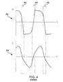
t1に対応する図は、交流電圧入力および結果として生じる電流の両方がゼロ値に達する時点を示している。この時点で、プラズマは活発に生成されてはいない。t2に対応する図は、ホロカソード302,304の間の電位差が最大に達し、プラズマ320が点火される時点を示している。t3に対応する図は、2つのホロカソード302,304の間にプラズマ320が完全に確立される、電流が最大となる時点を示している。t4に対応する図は、電流がt2の時点における電流と等しく、(t3に対応する図などと比較して)強度が低下したプラズマ320が存在するバイポーラホロカソード配置300を示している。t5に対応する図は、次のゼロ点交差を示し、この時点でプラズマ生成がいったん停止する。t6に対応する図は、プラズマ320が再び生成され、ホロカソード302およびホロカソード304の役割(陰極または陽極)がt2の場合とは逆になってサイクルが継続されることを示している。
The diagram corresponding to t 1 shows when both the AC voltage input and the resulting current reach a zero value. At this point, plasma is not actively generated. diagram corresponding to t 2, the potential difference between the
陰極と陽極との間の役割の切り替えについて簡単に説明する。まず、バイポーラ電源によって第1の電子放出面を負電圧に駆動してプラズマ形成を可能にするとともに、第2の電子放出面を電圧印加回路の陽極として機能するように正電圧に駆動する。その後、第1の電子放出面を正電圧に駆動し、陰極と陽極の役割を逆にする。電子放出面の1つが負に駆動されると、対応するキャビティ内で放電がなされる。他方のカソードが陽極となり、陰極側のホロカソードから陽極側のホロカソードに電子電流が流れる。 The role switching between the cathode and the anode will be briefly described. First, the first electron emission surface is driven to a negative voltage by a bipolar power source to enable plasma formation, and the second electron emission surface is driven to a positive voltage so as to function as an anode of a voltage application circuit. Thereafter, the first electron emission surface is driven to a positive voltage, and the roles of the cathode and the anode are reversed. When one of the electron emission surfaces is driven negative, a discharge occurs in the corresponding cavity. The other cathode becomes the anode, and an electron current flows from the holocathode on the cathode side to the holocathode on the anode side.
図4は、従来のバイポーラホロカソードプラズマ源における、プラズマなしの時間帯を示す。具体的には、図4では、電圧プロット202および電流プロット204に沿って、ホロカソード間でプラズマを活発に生成できるだけの十分な電位差が存在しない時間帯を特定する。非プラズマ生成帯402,404,406では、バイポーラホロカソード配置300は、それぞれの波周期の約25%の間、プラズマの生成を停止する。対照的に、本発明の実施形態による利点のひとつに、プラズマ生成用のホロカソード間に十分な電位差を維持することによって、本発明の実施形態ではプラズマが形成されない時間を短縮するか、排除することができる点がある。
FIG. 4 shows a time zone without plasma in a conventional bipolar holocathode plasma source. Specifically, in FIG. 4, a time zone in which there is not enough potential difference to actively generate plasma between the holocathodes is identified along the
図5は、本発明の実施形態による多相ホロカソードプラズマ源における、2つのホロカソード間の電圧プロットおよび電流プロットを示す。電圧プロット502,506,510および電流プロット504,508,512には、時点t10、t11、t12、t13、t14、t15が表示され、さまざまな着目点を示している。
FIG. 5 shows a voltage plot and a current plot between two holocathodes in a multiphase holocathode plasma source according to an embodiment of the present invention. The time points t 10 , t 11 , t 12 , t 13 , t 14 , and t 15 are displayed in the voltage plots 502, 506, 510 and the
図6は、本発明の実施形態による多相ホロカソードプラズマ源の異なる時点における断面図を示す。多相ホロカソード配置600は、ホロカソード602,604,606と、多相電源610とを含む。電源610によって電力が供給されると、ホロカソード602,604,606の間にプラズマ620が発生する。具体的には、2つのホロカソード602と604、604と606、602と606のそれぞれの間にプラズマ620が発生する。電圧プロット502,506,510および電流プロット504,508,512(図5に示す)はそれぞれ、2つのホロカソード602と604(図5では「A−B」と表示されている)、604と606(図5では「B−C」と表示されている)、602と606(図5では「A−C」と表示されている)の間の電圧および電流を示している(図6に示すホロカソードの組み合わせの場合)。電源610は交流電流を供給し、ホロカソード602,604,606は交互に陰極および陽極として機能する。この配置では、ホロカソード602と604、604と606の組み合わせでは位相が+120°ずれており、ホロカソード602と606の組み合わせでは位相が−120°ずれている。電圧プロット502,506,510および電流プロット504,508,512上には時点t10、t11、t12、t13、t14、t15が表示され、図6に示すホロカソード配置600の異なる図に対応するさまざまな着目点を示している。
FIG. 6 shows cross-sectional views at different times of a multiphase holocathode plasma source according to an embodiment of the present invention. The
任意の2つのホロカソード間で発生するプラズマは、両ホロカソード間の距離にいくらか影響される。いくつかの実施形態では、隣接する2つのホロカソード(たとえば、ホロカソード602と604、604と606の組み合わせ)間の距離は同一であるか、または実質的に同一であるが、隣接しないホロカソード(たとえば、602と606)間の距離は、隣接する2つの間の距離よりも長い。一対のホロカソード間の距離が長すぎると、両者間にプラズマが形成されないことがある。当業者であれば理解できるように、ホロカソード間の距離は、プロセス依存である。距離が増すにつれて、プラズマ形成に必要な電圧も大きくなる。いくつかの実施形態では、ホロカソード間の距離は、500mm未満または400mm未満、あるいは200mm未満である。いくつかの実施形態では、ホロカソード間の距離は約100mmである。これよりも長い距離でプラズマを形成できることもあるが、一般的なプロセスや電源では、最大距離は500mmであろう。また、有効な空間の範囲に、磁場が影響することもある。
The plasma generated between any two holocathodes is somewhat affected by the distance between the two holocathodes. In some embodiments, the distance between two adjacent holocathodes (eg, a combination of
発生するプラズマは、一対のホロカソード間の電圧および電流にもいくらか影響される。たとえば、複数対のホロカソード間にプラズマが生じることもあるが、ある程度、異なる組み合わせでのホロカソード間の電圧差および電流差がゆえ、プラズマ密度が均一にならない場合がある。プラズマ化学蒸着を用いた基板のコーティングに使用するには、たとえば、この不均一な状態はたいしたことがない。なぜなら、不均一な状態は短時間しか生じず、基板が明らかに移動するまでにプラズマ密度の高い領域と低い領域が何度も切り替わるからである。さらに、インラインコーティングプロセスでは、基板がプラズマ源の下を移動し、それぞれのホロカソードの下を通過するので、基板は均等に処理されることになる。 The generated plasma is somewhat affected by the voltage and current between the pair of holocathodes. For example, plasma may be generated between a plurality of pairs of holocathodes, but the plasma density may not be uniform due to the voltage and current differences between the holocathodes in different combinations to some extent. For example, this non-uniform state is unlikely to be used for coating a substrate using plasma enhanced chemical vapor deposition. This is because the non-uniform state occurs only for a short time, and the region where the plasma density is high and the region where the plasma density is low are switched many times before the substrate clearly moves. Furthermore, in the in-line coating process, the substrate is processed evenly as it moves under the plasma source and passes under each holocathode.
多相電源610は、単一の電源を含んでもよいし、複数の電源を含んでもよい。具体的には、多相電源610は、複数の出力波(たとえば、波形プロット100における波A、B、C)を形成することができ、この場合、複数の出力波(ならびに、これらの波が電力を供給するホロカソード)が各々、互いにタイミングがずれている。いくつかの実施形態では、隣接するホロカソード、たとえば2つのホロカソード602と604、604と606)の位相が互いに同じ位相角(たとえば、三相電源の場合は120°、四相電源の場合は90°、五相電源では72°、六相電源は60°、n相電源であればn分の360°)だけずれている。三相でホロカソードが3つあるリニアの実施形態(すなわち、ホロカソードが直線的に配置されている)では、隣接する2つのホロカソード602と604、604と606の位相が120°ずれていれば、隣接しない2つのホロカソード602と606は、位相が−120°ずれている。四相でホロカソードが4つあるリニアの実施形態では、隣接する2つの位相が60°ずれている場合、直線上で隣接しない第1および第3の2つのホロカソードでは位相が120°ずれており、直線上で隣接しない第1および第4の2つのホロカソードでは、位相が180°ずれている。
t10に対応する図は、ホロカソード602と604との間の電流が最大になる一方、ホロカソード604と606との間の電流が最大値の約半分となる時点を示している。t11に対応する図では、ホロカソード602と604との間の電流はゼロになり、ホロカソード602と606との間に電流が流れ始める。この同じ時点(t11)において、ホロカソード604と606の間の電流はその最大値に達する。サイクルは、ホロカソード602と606との間の電流が最大値に達し、t10に対応する図に示した方向とは逆方向ではあるがホロカソード602と604との間に電流が再び流れ始めるt12に対応する図において継続する。t13に対応する図は、ホロカソード602と604との間を流れる電流が最大になる一方、ホロカソード604と606との間の電流が最大値の約半分となるt10に対応する図からのサイクルの反対側の端を示す。t13に対応する図の電流は、t10に対応する図における電流とは逆方向に流れ、それまで陰極として機能していたホロカソードが、ここでは陽極として機能している。t14に対応する図は、電流がt11に対応する図で説明したものとは逆方向に流れる状況を示し、t15に対応する図は、電流がt12に対応する図で説明したものとは逆方向に流れる状況を示している。
diagram corresponding to t 10, while the current between the
図6(ならびに本発明の他の実施形態)に示す多相ホロカソード配置600のひとつの特徴として、電流が任意の2つのホロカソード間でゼロに近づく点のいずれにおいても、他の組み合わせでのホロカソード間の電圧差と電流がゼロではないことがあげられる。この配置では、バイポーラ電源で駆動される従来のプラズマ源における上述したプラズマなしの時間帯が生じないプラズマ装置を製造することが可能である。すなわち、本発明の実施形態では、上述のように、従来技術のバイポーラホロカソード配置300に固有の非プラズマ生成帯402,404,406を効果的に回避する。本発明の実施形態によれば、少なくとも3つのホロカソードと多相電源を含むことによって、稼働時間全体にわたって、電流と、それによって得られるプラズマ生成を維持することで連続的にプラズマを発生させる装置を含む、改良されたプラズマ特性が得られる。少なくとも3つの位相オフセット波と少なくとも3つのホロカソードを用いることにより、交流電源によって波が生じるプラズマなしの時間は実質的になくなることになる。パルス電力の場合、プラズマなしの時間は、設計上のパラメータに応じて実質的に0%から約20%になることがある。たとえば、少なくとも3つの位相オフセット波と少なくとも3つのホロカソードとを用いると、プラズマなしの時間が実質的に20%(あるいは、波の周期のうち80%の間は、プラズマが活発に発生する)、プラズマなしの時間が実質的に10%(あるいは、波の周期のうち90%の間は、プラズマが活発に発生する)、プラズマなしの時間が実質的に0%(あるいは、波の周期の100%でプラズマが活発に発生する)といった具合になり得る。プラズマに関連して減衰時間が存在する(すなわち、一対のホロカソード間で電圧がゼロまで降下した後ですら、プラズマが活発に生成されているわけではないにもかかわらず、電圧降下後の短時間、依然としてプラズマが存在する可能性がある)ため、本出願では、電子が活発に放出されている時間を、プラズマが活発に生成されているという。
One feature of the
いくつかの実施形態では、ホロカソード602,604,606(または本明細書に記載され、あるいは本明細書によって可能になる他のホロカソード配置)は、細長いキャビティを含んでもよい。ホロカソードは、プラズマ出口領域を含んでもよく、プラズマ出口領域は、単一のプラズマ出口オリフィスを含んでもよいし、複数のプラズマ出口オリフィスあるいはプラズマ出口溝を含んでもよく、これらのプラズマ出口領域のいくつかの組み合わせを含んでもよい。いくつかの実施形態では、ホロカソードは、ホロカソードおよびプラズマ出口領域の内面だけが電子を放出したり受け取ったりするように、それぞれ電気的に絶縁されている。いくつかの実施形態では、連続的に発生するプラズマは、実質的にすべて各ホロカソードのプラズマ出口領域を通って流れる。いくつかの実施形態では、電流は、二次電子放出または熱電子放出電子またはこれらの電流のいくつかの組み合わせからなる。いくつかの実施形態では、電位差がゆえにホロカソード間に電流が流れる。いくつかの実施形態では、この電位差は、任意の2つのホロカソード間で少なくとも50Vまたは少なくとも200Vである。いくつかの実施形態では、複数の出力波を形成する多相電源は、方形波からなる複数の出力波を生成し、それによって正弦波寄りも電位差が小さくなる。多相電源は、AC電気エネルギーの形態、パルス電気エネルギーの形態またはこれらの形態の電気エネルギーの何らかの組み合わせである。いくつかの実施形態では、発生するプラズマは、実質的に磁場駆動閉回路電子ドリフトが存在しない状態で、その長さ全体で実質的に均一である。いくつかの実施形態では、プラズマは、約0.1mから約1mまたは約1mから約4mの長さ全体で実質的に均一に発生する。いくつかの実施形態では、複数の出力波それぞれの周波数は等しく、約1kHz〜約1MHzまたは約10kHz〜約200kHzまたは約20kHz〜約100kHzの範囲内である。いくつかの実施形態では、放出面から放出される電子が、ホロカソード効果によって閉じ込められる。いくつかの実施形態では、放出面から放出される電子は、磁場によって閉じ込められない。
In some embodiments,
電子電流に影響をおよぼす1つの要因に、ホロカソードキャビティ壁の温度がある。キャビティ壁温度が1000℃未満のホロカソード構成では、電子放出は二次電子放出によって支配される。イオンがキャビティの壁に衝突すると、衝突するイオンの運動エネルギーと負の電位によって、壁面からの電子放出が誘発される。一般に、これらの「冷」ホロカソードは、キャビティ壁温度50℃〜500℃で稼働される。通常、ホロカソード構造をこのような温度に維持するには、冷却方法が適用される。ホロカソード構造内に水冷チャネルが組み込まれることも多い。冷ホロカソード放電用の動作電圧は一般に、300ボルトから1000ボルトである。 One factor that affects the electron current is the temperature of the holocathode cavity wall. In a holocathode configuration with a cavity wall temperature below 1000 ° C., electron emission is dominated by secondary electron emission. When ions collide with the cavity wall, electron emission from the wall surface is induced by the kinetic energy and negative potential of the colliding ions. In general, these “cold” holocathodes are operated at a cavity wall temperature of 50 ° C. to 500 ° C. Usually, cooling methods are applied to maintain the holocathode structure at such temperatures. Often, a water-cooled channel is incorporated into the holocathode structure. The operating voltage for cold holocathode discharge is typically 300 to 1000 volts.
あるいは、ホロカソードを熱電子モードで動作させてもよい。熱電子放出を発生させるためには、ホロカソードキャビティ壁の温度は通常1000℃〜2000℃の範囲である。熱電子ホロカソードでは、加熱を助けるためにキャビティ壁の周囲にヒータを組み込むようにしてもよいし、さらに簡単にするのであれば、プラズマエネルギーの伝達を利用してキャビティ壁を加熱してもよい。通常、熱伝導または放熱による熱の損失を低減するために、高温のキャビティは断熱されている。熱電子ホロカソード放電用の動作電圧は一般に、10ボルトから300ボルト、より一般的には10ボルトから100ボルトである。 Alternatively, the holocathode may be operated in the thermoelectron mode. In order to generate thermionic emission, the temperature of the holocathode cavity wall is usually in the range of 1000 to 2000 ° C. In the thermionic holocathode, a heater may be incorporated around the cavity wall to assist in heating, or for further simplification, the cavity wall may be heated using plasma energy transfer. Typically, hot cavities are insulated to reduce heat loss due to heat conduction or heat dissipation. The operating voltage for thermionic holocathode discharge is typically 10 to 300 volts, more typically 10 to 100 volts.
堆積率が十分に高く商業的に有用なPECVDプロセスでは、何らかの形で高密度化したプラズマに依存している。ホロカソード効果は、閉じた空間または部分的に閉じた空間における電界を利用して、電子を高密度化して閉じ込める具体的な方法のひとつである。負の電界を囲むことによって、気相である自由電子が捕捉され、周囲の壁または反対側の負にバイアスされた壁との間で振動運動をする。電子が振動すると電子の移動経路が長くなり、結果的に気相衝突の可能性が高くなる。このような衝突が生じると、気体分子がイオン化し、さらに電子と陽イオンが発生する。陽イオンは加速され、負にバイアスされたホロカソード壁に衝突する。壁に陽イオンが衝突すると、二次電子放出によってさらに電子が生じることになる。文献によれば、ホロカソードプラズマは通常、閉ドリフトでの電子閉じ込めプロセス(マグネトロンスパッタリングなど)で用いられるような、磁場による閉じ込めで得られるプラズマよりも密度の高いプラズマである。 A PECVD process with a sufficiently high deposition rate and commercially useful relies on some form of densified plasma. The holocathode effect is one of the specific methods for confining electrons with high density by using an electric field in a closed space or a partially closed space. By enclosing the negative electric field, free electrons in the gas phase are trapped and oscillate between the surrounding wall or the oppositely negatively biased wall. When electrons vibrate, the movement path of the electrons becomes longer, and as a result, the possibility of gas phase collision increases. When such a collision occurs, gas molecules are ionized, and electrons and cations are generated. The positive ions are accelerated and strike the negatively biased holocathode wall. When a cation collides with the wall, more electrons are generated by secondary electron emission. According to the literature, the holocathode plasma is usually a higher density plasma than that obtained by confinement by a magnetic field, such as used in an electron confinement process with closed drift (such as magnetron sputtering).
図6における実施形態の別の利点は、本発明の他の実施形態同様に、ホロカソードを増やすことにより、より広いプラズマが生成され、PECVDでの堆積率が改善されることにある。 Another advantage of the embodiment in FIG. 6 is that, like other embodiments of the invention, increasing the holocathode produces a wider plasma and improves the deposition rate in PECVD.
図7は、本発明の実施形態による方法を示す。多相ホロカソード配置600(および本開示に記載され、本開示によって可能になる他のホロカソード配置)を利用して、プラズマを連続的に発生させることができる。プラズマを発生させる方法700は、少なくとも3つのホロカソードを準備する工程(工程702)を含む。ホロカソードには各々、プラズマ出口領域がある。また、この方法は、複数の出力波を形成することができる電力源を準備することを含む(工程704)。この電力源には、各ホロカソードが電気的に接続されている。どのホロカソードも他のホロカソードとは電気的位相がずれるように、電力源によって生じた複数の出力波は位相のタイミングがずれている。電気的位相がずれている少なくとも3つのホロカソード間に、電流が流れる。ホロカソード間には、プラズマが連続的に生じる。いくつかの実施形態では、この方法は、基板を準備する工程(工程706)と、プラズマCVDを用いて基板にコーティングを施す工程(工程708)とをさらに含む。図7において工程706および708が点線で囲まれているのは、これらの工程が任意であることを示している。プラズマCVD(PECVD)を用いて基板にコーティングを施すことは、ホロカソードキャビティ内に、あるいはホロカソードに隣接するマニホールドを通して、原料ガス、プロセスガス、反応物ガスまたはこれらの組み合わせを準備することを含んでもよい。当業者であれば、PECVDに適用可能な他の工程を含んでもよいことも理解できるであろう。
FIG. 7 illustrates a method according to an embodiment of the invention. A multi-phase holocathode arrangement 600 (and other holocathode arrangements described in this disclosure and enabled by this disclosure) can be utilized to continuously generate a plasma. The
図8は、本発明の実施形態による方法によって形成されたコーティングを示す。コーティング802は、基板804の上に形成され、コーティングと基板との組み合わせ800となる。いくつかの実施形態では、基板804はガラスである。他の実施形態では、基板804は、プラスチック、金属、半導体材料またはPECVDプロセス用の他の適切な材料を含んでもよい。いくつかの実施形態では、コーティング802は単一の層またはフィルムであってもよいし、複数の層またはフィルムを含んでもよい。いくつかの実施形態では、コーティングと基板との組み合わせ800が建築での用途に適するように、コーティング802は低輻射コーティングであってもよく、基板804はガラス窓であってもよい。いくつかの実施形態では、コーティング802は、冷蔵庫のドアに使用される防曇コーティングまたは光電池に使用される透明な導電性酸化物コーティングなど、特定の用途のための別のコーティングであってもよい。
FIG. 8 shows a coating formed by a method according to an embodiment of the invention. The
図9は、本発明の実施形態によるプラズマ出口領域のあるホロカソードを含む多相ホロカソードプラズマ源を示す。直線状の多相ホロカソード配置600(図9に示す)は、ホロカソード602,604,606と、多相電源610とを含む。ホロカソード602,604,606は各々、ホロカソード同士の位相がずれるように、交流電源またはパルス電源によって多相電源610から電力を供給される。ホロカソード602,604,606はそれぞれ、ホロカソードキャビティ904と、プラズマ出力路902とを含む。図9に示す実施形態では、ホロカソード602,604,606は、互いに離隔した2つの側部領域と、キャビティ904を画定している上部領域と、プラズマ出力路902を画定している開放された底部領域とを含む。各ホロカソード602,604,606のホロカソードキャビティ904には、反応物ガス(またはプロセスガスまたは原料ガスまたはこれらの気体の組み合わせ)が存在してもよい。反応物ガス(またはプロセスガスまたは原料ガスまたはこれらの気体の組み合わせ)は、反応領域910に存在していてもよい。いくつかの実施形態では、反応領域910は基板804などの基板を含んでもよく、いくつかの実施形態では、反応領域910において基板にコーティングが形成されてもよい。多相電源610によって電力が供給されると、ホロカソード602,604,606各々の間で交互に電子が流れ、プラズマ出力路902から反応領域910に流出するプラズマを発生させる。
FIG. 9 illustrates a multiphase holocathode plasma source including a holocathode with a plasma exit region according to an embodiment of the present invention. The linear multiphase holocathode arrangement 600 (shown in FIG. 9) includes
図10は、本発明の実施形態による、溝状の限定されたプラズマ出口領域を有するホロカソードを含む多相ホロカソードプラズマ源を示す。図10の実施形態は、図9の実施形態の変更例であり、プラズマ出力路902が溝状のプラズマ出力路1002に置き換えられている。ホロカソード602,604,606はそれぞれ、ホロカソードキャビティ904と、プラズマ出力路1002とを含む。図10に示す実施形態では、ホロカソード602,604,606は、互いに離隔した2つの側部領域と、底部領域から離れた上部領域とを含み、プラズマ出力路1002が底部領域の溝によって画定されるようになっている。プラズマ出力路1002がゆえ、プロセスガスがホロカソードキャビティ904の中にあるときに、ホロカソード602,604,606内のガス圧をより高めることができる。
FIG. 10 illustrates a multi-phase holocathode plasma source including a holocathode having a grooved limited plasma exit region, according to an embodiment of the present invention. The embodiment of FIG. 10 is a modification of the embodiment of FIG. 9, and the
上述したように、本発明の実施形態による多相プラズマ源は、位相が互いにずれた3つのホロカソードすなわち三相でホロカソードが3つある実施形態を含むことができる。四相、五相または六相の実施形態といった他の実施形態も可能であり、一般に、n相の実施形態(nは2より大きい)で多相ホロカソード配置を提供可能であることは、当業者であれば理解できるであろう。追加のホロカソードと位相がずれた波を用いることで、所与のプロセスまたは用途に望ましい特性を持つプラズマを発生させることが可能になる。図9および図10の実施形態に示す(かつ、後述する)ように、本発明の実施形態によるn相のホロカソード配置は、m個のホロカソードを含むことができる(ここで、nはm以下である)。

図12は、本発明の実施形態による6つのホロカソードと3つの相を含む多相ホロカソードプラズマ源を示す。すなわち、本実施形態では、m=3、n=6である。ホロカソード配置1200は、多相電源1210に接続されたホロカソード1102,1104,1106,1108,1110,1112を含む。多相電源1210は、3つの位相オフセット波1220,1222,1224を形成する。この実施形態では、波1220はホロカソード1102と1108、波1222はホロカソード1104と1110、波1224はホロカソード1106と1112に電力を供給する。いくつかの実施形態では、波1220、1222、1224はそれぞれ、同じ位相角(たとえば、120°)だけオフセットしている。図12に示す実施形態では、隣接しない組み合わせである1102と1108、1104と1110、1106と1112は、互いに同相である。なぜなら、各組のホロカソードには、それぞれ同じ波1220、1222、1224から電力が供給されるためである。隣接する2つの位相が120°ずれている図12に示す2つのホロカソード間の位相差を、以下の表に示す。
FIG. 12 illustrates a multiphase holocathode plasma source including six holocathodes and three phases according to an embodiment of the present invention. That is, in this embodiment, m = 3 and n = 6. The
図13は、等間隔である3つのホロカソードを含む多相ホロカソードプラズマ源を示す。配置1300は、プラズマ出力路1002がそれぞれ共通の線に向けられた3つのホロカソード602,604,606を含む(図13は断面図であるので、それぞれの出力路が共通の点に向けられているように見える)。言うまでもなく、図13に示す実施形態には、各ホロカソード(またはホロカソードのいくつかのサブセット)のプラズマ出力路が同じ線(または同じ線の組)に向けられるようにして、さらに他のホロカソードを様々な幾何学的構成で含むこともできる。いくつかの実施形態では、ホロカソード間(隣接しているホロカソード間および隣接していないホロカソード間)の距離が等しい。たとえば、図13は、2つのホロカソード602と604との間の距離が、2つのホロカソード602と606、ホロカソード604と606との間の距離と実質的に同じであることを示している。いくつかの実施形態では、2つのホロカソード間の距離をホロカソードの中心から測定してもよいし、ホロカソードのプラズマ出力路から、あるいはホロカソードの中、上またはその付近の他の点から測定してもよい。図13に示す実施形態または類似の実施形態を使用すると、たとえばワイヤーまたは光ファイバーのコーティングなど、二次元の基材にコーティングを施すことができる。たとえば、このような細長い基材を同じ方向に通すことで、2次元の基材に均一にコーティングを施すことができる。
FIG. 13 shows a multiphase holocathode plasma source that includes three holocathodes that are equally spaced.
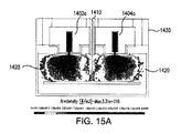
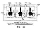
図14Aおよび図14Bは、本発明の実施形態によるバイポーラホロカソードプラズマ源と多相ホロカソードプラズマ源の両方におけるホロカソード内とその周囲でのプラズマ形成の電子密度を示す。図示のとおり、ホロカソードキャビティの外側すなわち反応領域における電子密度のレベルはバイポーラ(図14A)と多相プラズマ源(図14B)で同等であるのに対し、ホロカソードキャビティ内での電子密度は、多相プラズマ源よりもバイポーラプラズマ源の方が大幅に高い(図14B)。 14A and 14B show the electron density of plasma formation in and around the holocathode in both bipolar and multiphase holocathode plasma sources according to embodiments of the present invention. As shown, the level of electron density outside the holocathode cavity, ie in the reaction region, is equivalent for bipolar (FIG. 14A) and multiphase plasma source (FIG. 14B), whereas the electron density in the holocathode cavity is A bipolar plasma source is significantly higher than a multiphase plasma source (FIG. 14B).
図15Aおよび図15Bは、本発明の実施形態によるバイポーラホロカソードプラズマ源と多相ホロカソードプラズマ源の両方におけるホロカソード内とその周囲でのプラズマ形成のイオン密度を示す。図示のとおり、ホロカソードキャビティの外側すなわち反応領域におけるイオン密度のレベルはバイポーラ(図15A)と多相プラズマ源(図15B)で同等であるのに対し、ホロカソードキャビティ内でのイオン密度は、多相プラズマ源よりもバイポーラプラズマ源の方が大幅に高い(図15B)。 15A and 15B show the ion density of plasma formation in and around the holocathode for both bipolar and multiphase holocathode plasma sources according to embodiments of the present invention. As shown, the level of ion density outside the holocathode cavity, ie in the reaction region, is equivalent for bipolar (FIG. 15A) and multiphase plasma source (FIG. 15B), whereas the ion density in the holocathode cavity is A bipolar plasma source is significantly higher than a multiphase plasma source (FIG. 15B).
図16Aは、本発明の実施形態によるバイポーラホロカソードプラズマ源および多相ホロカソードプラズマ源の両方におけるホロカソードキャビティの壁に沿ったイオンの吸収量を示す。図示のとおり、ホロカソードキャビティの壁に沿ったイオンの吸収量は、多相プラズマ源よりもバイポーラプラズマ源の方が大幅に多い。また、同図は、ホロカソードキャビティの隅(指標値8、63、89、144)でイオンの吸収量が最低であることを示している。同図によれば、バイポーラ配置(この値は、たとえば、プラズマ源の稼働時に使用される電力レベルに応じて変化する)と比較して、多相配置のほうが吸収率は約88%低い。 FIG. 16A shows the absorption of ions along the walls of the holocathode cavity in both bipolar and multiphase holocathode plasma sources according to embodiments of the present invention. As shown, the amount of ions absorbed along the walls of the holocathode cavity is significantly greater in the bipolar plasma source than in the multiphase plasma source. This figure also shows that the amount of absorbed ions is the lowest at the corners (index values 8, 63, 89, 144) of the holocathode cavity. According to the figure, the absorptivity is about 88% lower in the multiphase arrangement compared to the bipolar arrangement (this value varies depending on, for example, the power level used when the plasma source is in operation).
図16Bは、図16Aのグラフに示すホロカソードキャビティの壁に沿った指標を示す。具体的には、図16Bでホロカソードキャビティ600の壁に沿って示された値は、図16Aにおけるx軸上の値に対応する(「キャビティ壁に沿った指標」)。
FIG. 16B shows an indicator along the wall of the holocathode cavity shown in the graph of FIG. 16A. Specifically, the values shown along the wall of the
図14から図16Bは、バイポーラホロカソード配置(配置300と同様)および多相ホロカソード配置(配置600と同様)の両方をシミュレーションした結果として得られたものである。たとえば、図14Aおよび図15Aを参照すると、このバイポーラ配置は、真空チャンバ1430内に位置する2つのリニアホロカソード1402a、1404a(逆位相)を含む。原料マニホールド1410を通って原料ガスが流れる。反応領域1420でプラズマが形成される。ここで、図14Bおよび図15Bを参照すると、この多相配置には、真空チャンバ1430内に位置する3つのリニアホロカソード1402b、1404b、1406b(互いに位相が120°オフセットしている)を含む。原料マニホールド1410を通って原料ガスが流れる。反応領域1420でプラズマが形成される。シミュレーションの設定について、以下でさらに説明する。ホロカソードキャビティでのプロセスガスにはアルゴンガスを使用した。本発明の実施形態によれば、酸素、窒素、アルゴン、ヘリウム、クリプトン、ネオン、キセノン、水素、フッ素、塩素およびそれらの混合物を含むが、これらに限定されない他のプロセスガスも使用できる。反応性のガスとしては、H2、H2O、H2O2、N2、NO2、N2O、NH3、CH4、CO、CO2、SH2、他の硫黄系ガス、ハロゲン、臭素、リン系ガス、それらの混合物があげられる。
14 to 16B are obtained as a result of simulating both a bipolar holocathode arrangement (similar to arrangement 300) and a multiphase holocathode arrangement (similar to arrangement 600). For example, referring to FIGS. 14A and 15A, this bipolar arrangement includes two linear holocathodes 1402a, 1404a (antiphase) located within a
具体的には、図14から図16Bを参照すると、ホロカソードの外側にあるプラズマ生成領域におけるプラズマ密度は、2相配置と3相配置のどちらも同レベルであるのに対し、(プラズマ密度およびイオン密度、イオンの吸収量によって示される)ホロカソードキャビティ内の摩耗のレベルは、本発明の実施形態による3相配置のほうが大幅に少ない。本発明の実施形態では、これによって、バイポーラプラズマ源よりもホロカソードのほうが動作寿命を長くすることができる。動作寿命は、他の要因の中でも、プラズマ源がどのようなプロセスに使用されているかに依存する。ガラスコーティングに関連する一般的なPECVDの用途では、従来のバイポーラ配置と比較して、三相でホロカソードが3つある配置では、想定される動作寿命が約60%の増加する形で改善されている。いくつかの実施形態では、これは寿命が約200時間長くなることに等しく、たとえば、ベースライン300時間に対して動作寿命500時間と同等となり得る。この利点は、単にホロカソードを追加した結果ではなく、多相電力配置としたことによるものである。 Specifically, referring to FIG. 14 to FIG. 16B, the plasma density in the plasma generation region outside the holocathode is the same level in both the two-phase arrangement and the three-phase arrangement (the plasma density and the ion density). The level of wear in the holocathode cavity (indicated by density, ion absorption) is significantly less in the three-phase arrangement according to embodiments of the present invention. In embodiments of the present invention, this can provide a longer operating life for the holocathode than for the bipolar plasma source. The operating lifetime depends on what process the plasma source is used for, among other factors. In a typical PECVD application related to glass coating, a three-phase, three holocathode arrangement improves the expected operating life by approximately 60% compared to a conventional bipolar arrangement. Yes. In some embodiments, this is equivalent to an increase in lifetime of about 200 hours, and may be equivalent to an operating lifetime of 500 hours for a baseline of 300 hours, for example. This advantage is not simply the result of adding a holocathode, but a multiphase power arrangement.
本発明者らは、ホロカソードキャビティ表面でのスパッタリング量が、数値シミュレーションで決定されるホロカソードキャビティ表面での反応性イオンの吸収量に関連していることを見いだした。 The present inventors have found that the amount of sputtering at the holocathode cavity surface is related to the amount of reactive ions absorbed at the holocathode cavity surface determined by numerical simulation.
ガス流とガス放電のシミュレーションに用いたシミュレーションソフトウェアは、ドイツのBraunschweigにあるFraunhofer−Institute for Surface Engineering and Thin Films ISTによって開発されたPIC−MCと呼ばれるプログラムである。このソフトウェアでは、ガス流、磁場、プラズマのシミュレーションを組み合わせている。そこでは、ガス流のシミュレーションでは、直接シミュレーションモンテカルロ(DSMC)法が用いられ、磁場のシミュレーションでは境界要素法(BEM)、プラズマシミュレーションではセル内粒子モンテカルロ法(PIC−MC)が用いられている。 The simulation software used for the simulation of gas flow and gas discharge is a program called PIC-MC developed by Fraunhofer-Institute for Surface Engineering and Thin Films IST in Braunschweig, Germany. This software combines gas flow, magnetic field and plasma simulations. There, the direct simulation Monte Carlo (DSMC) method is used for gas flow simulation, the boundary element method (BEM) is used for magnetic field simulation, and the in-cell particle Monte Carlo method (PIC-MC) is used for plasma simulation.
ホロカソードプラズマ源を横方向に1.016mm厚で切った切片である擬似2Dモデルを使用して、シミュレーションを行った。擬似2Dは、切片の厚みが小さく、それぞれの面に対して横方向に一定の周期で条件が適用されることを意味する。 The simulation was performed using a pseudo 2D model, which is a section obtained by cutting a holocathode plasma source in the transverse direction with a thickness of 1.016 mm. Pseudo 2D means that the thickness of the slice is small, and the condition is applied at a constant period in the transverse direction with respect to each surface.
シミュレーションには、プラズマを形成する多くの異なるガスを用いることができ、先の例ではアルゴンを使用した。計算時間を制限するために、コーティング原料としてSi2H6を選択し、それによって生じうる反応のうち、以下の2つを選択した。
Si2H6+e− → Si2H4 ++2H+2e− (1)
Si2H6+e− → SiH3+SiH2+H+e− (2)
Many different gases that form the plasma can be used for the simulation, argon was used in the previous example. In order to limit the calculation time, Si 2 H 6 was selected as the coating raw material, and the following two were selected from the reactions that could occur.
Si 2 H 6 + e − → Si 2 H 4 + + 2H + 2e − (1)
Si 2 H 6 + e − → SiH 3 + SiH 2 + H + e − (2)
水素種は、シミュレーションに含めなかった。 Hydrogen species were not included in the simulation.
入力パラメータの各セットについて、シミュレーションでは、異なる気相種(原子、イオン、分子、電子)が占有する空間全体における、それらの気相種の数と速度に関するデータが得られる。このデータから、密度やフラックスなど、何らかの値を計算することができる。ここで、フラックスとは、単位面積あたりの気相種の流動率である(単位:mol・m-2・s-1)。 For each set of input parameters, the simulation provides data on the number and velocity of these gas phase species in the entire space occupied by different gas phase species (atoms, ions, molecules, electrons). From this data, some values such as density and flux can be calculated. Here, the flux is the flow rate of gas phase species per unit area (unit: mol · m −2 · s −1 ).
もうひとつの有用な計算値として、表面で吸収されるフラックスがある。カソードキャビティ材料の何らかの固着係数があれば、その表面に向けられたイオンフラックスから、表面でのイオンの吸収量を計算することができる。バイポーラホロカソードの動作によって得られる結果をシミュレーションデータと相関させることにより、本発明者らは、シミュレーションモデルによれば実際のプラズマ源で観察されるデブリの形成、ひいてはキャビティの表面でのスパッタリングが、ホロカソードキャビティの表面におけるイオン化プラズマ種の吸収レベルに関連していることを見いだした。 Another useful calculation is the flux absorbed at the surface. Given some anchoring factor for the cathode cavity material, the amount of ions absorbed at the surface can be calculated from the ion flux directed at that surface. By correlating the results obtained by the operation of the bipolar holocathode with the simulation data, the inventors have found that according to the simulation model, the formation of debris observed in the actual plasma source, and thus the sputtering at the surface of the cavity, We found that it is related to the absorption level of ionized plasma species at the surface of the holocathode cavity.
アルゴンの吸収量は、使用したプラズマシミュレーションで容易に導き出される特性のひとつである。さらに、アルゴンの吸収量は、電極表面に入射する粒子フラックスとイオンエネルギーを示す有効な指標である。当業者であれば、イオンエネルギーと粒子フラックスが、スパッタリングや電極侵食といった物理的プロセスの引き金となる主な要因であることを理解するであろう。デブリは、近傍の表面からスパッタされる材料の堆積量とスパッタ率とのバランスが正味の堆積量に偏っている場合に発生する。この作用は、図16Aおよび図16Bで観察できる。同図には、(シミュレーションによって)イオンの吸収量が最低であると判明した矩形電極の隅で正味の堆積量とスパッタが少ないことが示されている。 The amount of argon absorbed is one of the characteristics that can be easily derived from the plasma simulation used. Furthermore, the absorption amount of argon is an effective index indicating the particle flux and ion energy incident on the electrode surface. One skilled in the art will understand that ion energy and particle flux are the main factors that trigger physical processes such as sputtering and electrode erosion. Debris occurs when the balance between the deposition amount of the material sputtered from the nearby surface and the sputtering rate is biased toward the net deposition amount. This effect can be observed in FIGS. 16A and 16B. The figure shows that there is less net deposition and spatter at the corners of the rectangular electrode where the absorption of ions was found to be minimal (by simulation).
このようにシミュレーションでは実際のスパッタリング値を測定するわけではないが、本発明者らは、本明細書に記載する多相の実施形態でのスパッタリングまたは電極侵食の指標として、アルゴンの吸収値を使用した。 Thus, although the simulation does not measure the actual sputtering value, we use the argon absorption value as an indicator of sputtering or electrode erosion in the multiphase embodiments described herein. did.
ホロカソードのキャビティ表面で吸収されるイオン化プラズマ種が低レベルであるということは、キャビティでのスパッタリングレベルが低く、デブリ形成が少ないことを意味する。図16Aおよび図16Bに示すように、プロセスチャンバでのバイポーラプラズマ源と多相プラズマ源の両方のプラズマエネルギーが等しくなる大部分の電極表面において、バイポーラプラズマ源でスパッタリングと摩耗量が増大していた。バイポーラプラズマ源から材料がさらにスパッタリングされると、電極キャビティの隅やプラズマ源の外にある(浮遊しているか接地電位にあってスパッタリングの対象とならない)表面など、強いスパッタリングが生じていない表面に被着したときに、デブリをさらに増す可能性がある。こうしたデブリの性質および量は、電極の表面材料とプラズマガスとの組み合わせに大きく左右される。 A low level of ionized plasma species absorbed at the cavity surface of the holocathode means a low level of sputtering in the cavity and less debris formation. As shown in FIGS. 16A and 16B, sputtering and wear increased in the bipolar plasma source on most electrode surfaces where the plasma energy of both bipolar and multiphase plasma sources in the process chamber were equal. . When material is further sputtered from a bipolar plasma source, it can be applied to surfaces that are not subject to strong sputtering, such as the corners of electrode cavities and surfaces outside the plasma source (floating or grounded and not subject to sputtering). When deposited, it can further increase debris. The nature and amount of such debris is highly dependent on the combination of electrode surface material and plasma gas.
別の重要な量として、発生する電子密度がある。電子密度は表面処理またはコーティング効率に大きな影響を与え、電子密度が高いほど表面処理またはコーティング効率も高くなる。本シミュレーションでは、プラズマ源を支持するチャンバ構造から2.54mmの距離に設定したライン上の真空チャンバで電子密度を決定し、これを平均した。 Another important quantity is the generated electron density. The electron density has a great influence on the surface treatment or coating efficiency, and the higher the electron density, the higher the surface treatment or coating efficiency. In this simulation, the electron density was determined in a vacuum chamber on a line set at a distance of 2.54 mm from the chamber structure supporting the plasma source and averaged.
本発明者らは、驚くべきことに、位相が120°ずつシフトしている3つのホロカソードを用いた場合に、位相が180°シフトしている2つのホロカソードのある構成と比較して、カソードキャビティの表面で吸収されるイオン化プラズマ種のレベルが低くなることを見いだした。 The inventors surprisingly found that when using three holocathodes with a phase shift of 120 °, the cathode cavity compared to one configuration with two holocathodes with a phase shift of 180 °. We have found that the level of ionized plasma species absorbed at the surface of the metal is low.
本発明のこの実施形態によれば、本発明者らは、驚くべきことに、三相で3つのホロカソードを配置した場合と二相で2つのホロカソードを配置した場合では、ホロカソードの外側にある反応領域での電子密度は同じような強度であることを見いだした。これは、驚くべきことである。なぜなら、たとえば三相で3つのホロカソードを配置すると、2相で2つのホロカソードを配置するよりもプラズマが集中する面積が大きくなり、ホロカソード内での摩耗が減るからである。 According to this embodiment of the present invention, the inventors surprisingly found that the reaction outside the holocathode was observed when three holocathodes were arranged in three phases and two holocathodes were arranged in two phases. We found that the electron density in the region is similar. This is surprising. This is because, for example, if three holocathodes are arranged in three phases, the area where plasma is concentrated becomes larger than that in which two holocathodes are arranged in two phases, and wear in the holocathodes is reduced.
当業者が本開示から理解するように、特定の配置を特定の用途に適するように設計してホロカソードおよび多相電力入力を他の多くの形で組み合わせることが可能である。 As those skilled in the art will appreciate from the present disclosure, a particular arrangement can be designed to suit a particular application, and the holocathode and multiphase power input can be combined in many other ways.
以上、さまざまな実施形態について説明したが、いずれも限定的なものではなく、単なる例示として示したものにすぎない点を理解されたい。したがって、本開示の範囲および意図は、上記の例示的な実施形態のいずれによっても限定されるべきではない。さらに、本明細書中で他に示されるか文脈から明らかに矛盾しない限り、すべての可能な変形例における上記の要素の任意の組み合わせが、本開示に包含される。 While various embodiments have been described above, it should be understood that all are not limiting and are merely exemplary. Accordingly, the scope and spirit of the present disclosure should not be limited by any of the above-described exemplary embodiments. Moreover, any combination of the above-described elements in all possible variations thereof is encompassed by the disclosure unless otherwise indicated herein or otherwise clearly contradicted by context.
さらに、上記にて説明して図示したプロセスは、一連の工程として示されているが、これは説明の便宜上のものである。したがって、いくつかの工程を追加してもよいし、いくつかの工程を省略してもよく、工程の順序を変えたり、いくつかの工程を同時並行で実施したりしてもよい。
Furthermore, although the process described and illustrated above is shown as a series of steps, this is for convenience of explanation. Therefore, some steps may be added, some steps may be omitted, the order of steps may be changed, and some steps may be performed simultaneously.
Claims (69)
第1の出力波と、第2の出力波と、第3の出力波と、を含む、複数の出力波を形成することのできる電力源と、を備えるプラズマ源であって、
前記第1の出力波と前記第2の出力波は位相がずれており、前記第2の出力波と前記第3の出力波は位相がずれており、前記第1の出力波と前記第3の出力波は位相がずれており、
前記ホロカソードは各々、前記第1のホロカソードが前記第1の出力波に電気的に接続され、前記第2のホロカソードが前記第2の出力波に電気的に接続され、前記第3のホロカソードが前記第3の出力波に電気的に接続されるようにして、前記電力源に電気的に接続され、
電気的位相がずれている前記少なくとも3つのホロカソード間に電流が流れ、
前記プラズマ源は、前記ホロカソード間にプラズマを発生させることができる、プラズマ源。 At least three holocathodes comprising a first holocathode, a second holocathode, and a third holocathode, each having a plasma exit region;
A plasma source comprising a power source capable of forming a plurality of output waves, including a first output wave, a second output wave, and a third output wave,
The first output wave and the second output wave are out of phase, the second output wave and the third output wave are out of phase, and the first output wave and the third output wave are out of phase. The output wave of is out of phase,
Each of the holocathodes is electrically connected to the first output wave, the second holocathode is electrically connected to the second output wave, and the third holocathode is electrically connected to the first output wave. Electrically connected to the power source so as to be electrically connected to a third output wave;
A current flows between the at least three holocathodes that are out of electrical phase;
The plasma source can generate plasma between the holocathodes.
第1の出力波と、第2の出力波と、第3の出力波と、を含む、複数の出力波を形成することのできる電力源を準備することを含む、プラズマを発生させる方法であって、
前記第1の出力波と前記第2の出力波は位相がずれており、前記第2の出力波と前記第3の出力波は位相がずれており、前記第1の出力波と前記第3の出力波は位相がずれており、
前記ホロカソードは各々、前記第1のホロカソードが前記第1の出力波に電気的に接続され、前記第2のホロカソードが前記第2の出力波に電気的に接続され、前記第3のホロカソードが前記第3の出力波に電気的に接続されるようにして、前記電力源に電気的に接続され、
電気的位相がずれている前記少なくとも3つのホロカソード間に電流が流れ、
プラズマは、前記ホロカソード間で発生する、方法。 Providing at least three holocathodes, each including a first holocathode, a second holocathode, and a third holocathode, each having a plasma exit region;
A method for generating plasma, comprising preparing a power source capable of forming a plurality of output waves, including a first output wave, a second output wave, and a third output wave. And
The first output wave and the second output wave are out of phase, the second output wave and the third output wave are out of phase, and the first output wave and the third output wave are out of phase. The output wave of is out of phase,
Each of the holocathodes is electrically connected to the first output wave, the second holocathode is electrically connected to the second output wave, and the third holocathode is electrically connected to the first output wave. Electrically connected to the power source so as to be electrically connected to a third output wave;
A current flows between the at least three holocathodes that are out of electrical phase;
A method wherein plasma is generated between the holocathodes.
プラズマ化学蒸着を用いて前記基板にコーティングを形成することをさらに含む、請求項35に記載の方法。
Prepare the board
36. The method of claim 35, further comprising forming a coating on the substrate using plasma enhanced chemical vapor deposition.
Applications Claiming Priority (5)
| Application Number | Priority Date | Filing Date | Title |
|---|---|---|---|
| US14/942,673 | 2015-11-16 | ||
| US14/942,737 | 2015-11-16 | ||
| US14/942,673 US9721764B2 (en) | 2015-11-16 | 2015-11-16 | Method of producing plasma by multiple-phase alternating or pulsed electrical current |
| US14/942,737 US9721765B2 (en) | 2015-11-16 | 2015-11-16 | Plasma device driven by multiple-phase alternating or pulsed electrical current |
| PCT/US2016/061134 WO2017087233A1 (en) | 2015-11-16 | 2016-11-09 | Plasma device driven by multiple-phase alternating or pulsed electrical current and method of producing a plasma |
Publications (1)
| Publication Number | Publication Date |
|---|---|
| JP2018535532A true JP2018535532A (en) | 2018-11-29 |
Family
ID=58717680
Family Applications (1)
| Application Number | Title | Priority Date | Filing Date |
|---|---|---|---|
| JP2018544766A Pending JP2018535532A (en) | 2015-11-16 | 2016-11-09 | Plasma device driven by polyphase alternating current or pulsed current and method for generating plasma |
Country Status (10)
| Country | Link |
|---|---|
| EP (1) | EP3377673A4 (en) |
| JP (1) | JP2018535532A (en) |
| KR (1) | KR20180095530A (en) |
| CN (1) | CN108463575A (en) |
| BR (1) | BR112018009864A8 (en) |
| EA (1) | EA201891175A1 (en) |
| MX (1) | MX2018006095A (en) |
| PH (1) | PH12018501049A1 (en) |
| SG (1) | SG11201804129YA (en) |
| WO (1) | WO2017087233A1 (en) |
Families Citing this family (2)
| Publication number | Priority date | Publication date | Assignee | Title |
|---|---|---|---|---|
| RU2680318C1 (en) * | 2018-08-31 | 2019-02-19 | Общество С Ограниченной Ответственностью "Трипл-Сп" | Ac high-voltage electric arc plasma torch cooling system and the ac high-voltage electric arc plasma torch with cooling system (embodiments) |
| CN115355504A (en) * | 2022-08-15 | 2022-11-18 | 浙江大学台州研究院 | Multiphase alternating current plasma torch and solid waste treatment device |
Family Cites Families (7)
| Publication number | Priority date | Publication date | Assignee | Title |
|---|---|---|---|---|
| JPH07226395A (en) * | 1994-02-15 | 1995-08-22 | Matsushita Electric Ind Co Ltd | Vacuum plasma treatment apparatus |
| US7232975B2 (en) * | 2003-12-02 | 2007-06-19 | Battelle Energy Alliance, Llc | Plasma generators, reactor systems and related methods |
| US7411353B1 (en) * | 2007-05-11 | 2008-08-12 | Rutberg Alexander P | Alternating current multi-phase plasma gas generator with annular electrodes |
| CN105206496B (en) * | 2008-08-04 | 2019-07-05 | 北美Agc平板玻璃公司 | Plasma source and with the chemical vapor deposition of plasma enhancing come the method for depositing thin film coatings |
| US20120164353A1 (en) * | 2009-09-05 | 2012-06-28 | John Madocks | Plasma enhanced chemical vapor deposition apparatus |
| HUE049078T2 (en) * | 2012-11-02 | 2020-09-28 | Agc Inc | Plasma source for a plasma cvd apparatus and a manufacturing method of an article using the plasma source |
| WO2015022621A1 (en) * | 2013-08-11 | 2015-02-19 | Ariel - University Research And Development Company, Ltd. | Ferroelectric emitter for electron beam emission and radiation generation |
-
2016
- 2016-11-09 CN CN201680078860.4A patent/CN108463575A/en active Pending
- 2016-11-09 MX MX2018006095A patent/MX2018006095A/en unknown
- 2016-11-09 EP EP16866871.3A patent/EP3377673A4/en not_active Withdrawn
- 2016-11-09 JP JP2018544766A patent/JP2018535532A/en active Pending
- 2016-11-09 EA EA201891175A patent/EA201891175A1/en unknown
- 2016-11-09 KR KR1020187017067A patent/KR20180095530A/en unknown
- 2016-11-09 WO PCT/US2016/061134 patent/WO2017087233A1/en active Application Filing
- 2016-11-09 BR BR112018009864A patent/BR112018009864A8/en not_active Application Discontinuation
- 2016-11-09 SG SG11201804129YA patent/SG11201804129YA/en unknown
-
2018
- 2018-05-16 PH PH12018501049A patent/PH12018501049A1/en unknown
Also Published As
| Publication number | Publication date |
|---|---|
| BR112018009864A2 (en) | 2018-11-13 |
| MX2018006095A (en) | 2018-11-12 |
| EA201891175A1 (en) | 2018-12-28 |
| BR112018009864A8 (en) | 2019-02-26 |
| WO2017087233A1 (en) | 2017-05-26 |
| SG11201804129YA (en) | 2018-06-28 |
| EP3377673A1 (en) | 2018-09-26 |
| KR20180095530A (en) | 2018-08-27 |
| CN108463575A (en) | 2018-08-28 |
| EP3377673A4 (en) | 2019-07-31 |
| PH12018501049A1 (en) | 2019-01-28 |
Similar Documents
| Publication | Publication Date | Title |
|---|---|---|
| US10559452B2 (en) | Plasma device driven by multiple-phase alternating or pulsed electrical current | |
| JP6710686B2 (en) | Hollow cathode plasma source, substrate treatment method | |
| JP6313265B2 (en) | Plasma source | |
| EP2368257A2 (en) | Closed drift magnetic field ion source apparatus containing self-cleaning anode and a process for substrate modification therewith | |
| US10242846B2 (en) | Hollow cathode ion source | |
| JP2018535532A (en) | Plasma device driven by polyphase alternating current or pulsed current and method for generating plasma | |
| EP3619734B1 (en) | Linear plasma source with segmented hollow cathode | |
| US9721764B2 (en) | Method of producing plasma by multiple-phase alternating or pulsed electrical current | |
| JP2019501496A (en) | Holocathode ion source and method for extracting and accelerating ions | |
| Abidat et al. | Numerical simulation of atmospheric dielectric barrier discharge in helium gas using COMSOL Multiphysics | |
| Gao et al. | Comparing Study on Formation of Large Discharge Currents in Atmospheric Pulse-Modulated Radio Frequency Discharges | |
| KR100485816B1 (en) | High pressure plasma discharge device | |
| JP2020047591A (en) | Hollow cathode plasma source | |
| Velasco et al. | Electron cyclotron resonance discharge as a source for hydrogen and deuterium ions production | |
| KR20050006095A (en) | High pressure plasma discharge device |