JP2020047591A - Hollow cathode plasma source - Google Patents
Hollow cathode plasma source Download PDFInfo
- Publication number
- JP2020047591A JP2020047591A JP2019212122A JP2019212122A JP2020047591A JP 2020047591 A JP2020047591 A JP 2020047591A JP 2019212122 A JP2019212122 A JP 2019212122A JP 2019212122 A JP2019212122 A JP 2019212122A JP 2020047591 A JP2020047591 A JP 2020047591A
- Authority
- JP
- Japan
- Prior art keywords
- plasma source
- plasma
- hollow cathode
- hole
- cross
- Prior art date
- Legal status (The legal status is an assumption and is not a legal conclusion. Google has not performed a legal analysis and makes no representation as to the accuracy of the status listed.)
- Pending
Links
Images


Landscapes
- Plasma Technology (AREA)
- Chemical Vapour Deposition (AREA)
Abstract
Description
関連出願へのクロスリファレンス
本出願は、本出願と同日に出願され、本明細書に援用される、発明の名称が「Plasma Source Utilizing a Macro−Particle Reduction Coating and Method of Using a Plasma Source Utilizing a Macro−Particle Reduction Coating for Deposition of Thin Film Coatings and Modification of Surfaces」であるPCT国際出願第____号(未譲渡)(代理人整理番号0124−374.PCT)に関する。
CROSS REFERENCE TO RELATED APPLICATIONS This application is filed on the same day as the present application and is hereby incorporated by reference herein, under the name of "Plasma Source Utilizing a Macro-Particle Reduction Coating and Method of Medicine in the United States of America." -PCT International Application _____________________________________________________________________ entitled, "Particle Reduction Coating for Deposition of Thin Film Coatings and Modification of Surfaces" (Attorney Docket No. 0124-374.PCT).
本発明は、大きな基材の表面処理および/またはコーティング用のプラズマ源に関する。特に、本発明は、プラズマ強化化学蒸着およびプラズマ表面処理用のリニアプラズマ源、特に中空陰極タイプの放電を利用したプラズマ源に関する。 The present invention relates to a plasma source for surface treatment and / or coating of large substrates. In particular, the present invention relates to linear plasma sources for plasma enhanced chemical vapor deposition and plasma surface treatment, and more particularly to a plasma source utilizing a hollow cathode type discharge.
薄膜の付着および表面の化学的改質のための様々なプラズマ源が、従来技術において開示されている。 Various plasma sources for thin film deposition and surface chemical modification have been disclosed in the prior art.
大きな基材を処理する場合、これらのプラズマ源は一般に、Madocksに付与された米国特許第7411352号に開示されているようなリニアイオン源である。このプラズマ源はマグネトロン放電を利用しており、リニアイオンビームを発生させるか、複数のプラズマ源の組み合わせによって、基材の表面に向けられる複数の平行なイオンビームを発生させる。Madocksは、コーティング目的で、プラズマ源の外でコーティング原料を提供できることを開示している。プラズマは本質的に一次元すなわち、プラズマ源の長さに沿ってのみ延びる。イオンビームの幅は、平均自由行程長を制限するプロセスチャンバ内の圧力による制約を受ける。このため、このプラズマ源の下で基材を搬送するとき、接触時間は比較的短い。従って、例えばプラズマで基材を処理する時間を長くする必要がある場合には、プラズマ源の数を増やさなければならなくなる。さらに、プラズマ源に隣接して注入されるコーティング原料には、プラズマビームと相互作用する機会が限られる。この結果、付着率が比較的低くなり、基材表面と反応できなかった原料でコーターを汚してしまう危険性が増す。 When processing large substrates, these plasma sources are generally linear ion sources as disclosed in U.S. Pat. No. 7,411,352 to Madocks. The plasma source utilizes a magnetron discharge to generate a linear ion beam or a combination of a plurality of plasma sources to generate a plurality of parallel ion beams directed at the surface of the substrate. Madocks discloses that coating materials can be provided outside the plasma source for coating purposes. The plasma extends essentially only in one dimension, ie, along the length of the plasma source. The width of the ion beam is constrained by the pressure in the process chamber which limits the mean free path length. For this reason, when transporting a substrate under this plasma source, the contact time is relatively short. Thus, for example, if it is necessary to increase the time for treating a substrate with plasma, the number of plasma sources must be increased. Further, the coating material injected adjacent to the plasma source has a limited opportunity to interact with the plasma beam. As a result, the adhesion rate becomes relatively low, and the danger of contaminating the coater with a raw material that has failed to react with the substrate surface increases.
また、Madocksは、電極材料のスパッタリングが起こり、スパッタされた材料が再付着してプラズマ源の中にとどまることを開示している。しかしながら、電極材料がスパッタリングされると、電極の寿命が短くなる。スパッタされた材料の再付着によって、プラズマ源のノズルがふさがり、均一な基材処理またはコーティングが不可能になるおそれもある。さらに、スパッタリングされた電極材料がさらに凝縮および/または反応して、プラズマ源のノズルをふさいだり、基材上に落ちて欠陥を生じたりするデブリが形成される場合がある。これらのノズルは、プラズマ源の電極のうちの1つによって構成されている。このため電極は、真空チャンバ内のコーティングプロセス環境に曝露され、よって、注入されたコーティング原料で汚れやすい。 Madocks also discloses that sputtering of the electrode material occurs and the sputtered material re-adheres and remains in the plasma source. However, when the electrode material is sputtered, the life of the electrode is shortened. Redeposition of the sputtered material can also block the nozzle of the plasma source, making uniform substrate processing or coating impossible. In addition, the sputtered electrode material may further condense and / or react to form debris that may block the nozzle of the plasma source or fall onto the substrate and cause defects. These nozzles are constituted by one of the electrodes of the plasma source. For this reason, the electrodes are exposed to the coating process environment in the vacuum chamber and are therefore prone to contamination with the injected coating material.
さらに、Madocksによって開示されたマグネトロン放電を利用したプラズマ源には、磁石が必要である。磁石は高温に影響されやすいため、このようなプラズマ源を高温で動作させることができず、能動的または受動的手段によって冷却する必要がある。これらの磁石が存在するだけでなく、シャントを存在させる必要もあることから、複雑で高価なアセンブリになる。 Furthermore, the magnet source disclosed in Madocks using a magnetron discharge requires a magnet. Because magnets are sensitive to high temperatures, such plasma sources cannot be operated at high temperatures and must be cooled by active or passive means. Not only are these magnets present, but also the need for shunts, resulting in a complex and expensive assembly.
また、このプラズマ源は、中空陰極放電を利用したプラズマ源と比較して、比較的低密度で自由電子を発生させる。コーティングの目的で、プラズマの電子はコーティング原料をイオン化する働きをする。このため、Madocksによって開示されたものなどのマグネトロンプラズマを利用したプラズマ源を用いると、コーティング効率が低くなる。 Further, this plasma source generates free electrons at a relatively low density as compared with a plasma source using a hollow cathode discharge. For the purpose of coating, the plasma electrons serve to ionize the coating material. Thus, using a plasma source that utilizes magnetron plasma, such as that disclosed by Madocks, reduces coating efficiency.
Jungは、欧州特許出願公開第0727508号(A1)において、2つの平行な電極を利用した中空陰極リニアプラズマ源を開示している。プラズマは本質的に一次元すなわち、プラズマ源の長さに沿ってのみ延び、狭いプラズマビームを形成する。Jungは、電極材料のスパッタリングを避けるために、不活性ガス流を電極に平行に注入しなければならないことを開示している。しかしながら、電極に平行な不活性ガスの注入は、反応性イオンの発生率低下につながるため、処理効率またはコーティング率が低下する。 Jung, in EP-A-0 727 508 (A1), discloses a hollow cathode linear plasma source utilizing two parallel electrodes. The plasma extends essentially only in one dimension, ie, along the length of the plasma source, forming a narrow plasma beam. Jung discloses that a stream of inert gas must be injected parallel to the electrodes to avoid sputtering of the electrode material. However, the injection of an inert gas parallel to the electrodes leads to a decrease in the rate of generation of reactive ions, thereby reducing the processing efficiency or the coating rate.
堆積率の高いこの種のプラズマ源の主な問題の1つに、プラズマ源の壁が、プラズマを通って流れる原料と早い段階で反応することによってすぐに汚れてしまうという事実がある。この問題がゆえ、当該プロセスの工業利用は非常に限られており、生産ラインにおけるスループットに対する制約となる頻繁な洗浄サイクルが必要である。 One of the main problems with this type of high deposition rate plasma source is the fact that the walls of the plasma source quickly become fouled by reacting early with the raw material flowing through the plasma. Due to this problem, the industrial application of the process is very limited and requires frequent cleaning cycles which limit throughput on the production line.
堆積率の高いこれらのプラズマ源の別の欠点として、原料がプラズマ源を離れた後にこれを基材の表面だけにとどめておくのが困難なことがあげられる。結果として、原料のかなりの部分は、基材にコーティングを形成するのに使用できない。これは、プラズマ源を取り囲む表面での原料の変化に伴うコーティング率の低下とコーターの汚れにつながる。 Another disadvantage of these high deposition rate plasma sources is that it is difficult for the source to remain on the surface of the substrate only after leaving the plasma source. As a result, a significant portion of the raw material cannot be used to form a coating on the substrate. This leads to a decrease in coating rate and a fouling of the coater due to changes in the raw material on the surface surrounding the plasma source.
したがって、大面積での表面処理および大面積でのコーティングの分野では、大きな基材を高効率かつ少ない量の汚染と欠陥で処理および/またはコーティングできるかなりの長さの均一なプラズマを提供可能な単純なプラズマ源が、依然として必要とされている。 Thus, in the field of large area surface treatments and large area coatings, it is possible to provide a fairly long, uniform plasma capable of treating and / or coating large substrates with high efficiency and low amounts of contamination and defects. A simple plasma source is still needed.
本発明の一態様では、大きな基材への薄膜の付着と大きな基材の表面のプラズマ処理に有用なリニアプラズマ源が提供される。プラズマ処理とは、例えば、表面活性化、表面洗浄および表面エッチングを包含することを意味する。 In one aspect of the present invention, a linear plasma source is provided that is useful for depositing a thin film on a large substrate and for plasma treating the surface of the large substrate. Plasma treatment is meant to include, for example, surface activation, surface cleaning and surface etching.
本発明の一態様では、リニアプラズマが非常に広い、中空陰極を利用したプラズマ源が提供される。
本発明の一態様では、均一で幅広いリニアプラズマを形成することができるプラズマ源が提供される。
In one aspect of the present invention, a plasma source utilizing a hollow cathode, wherein the linear plasma is very wide, is provided.
In one embodiment of the present invention, a plasma source capable of forming a uniform and wide linear plasma is provided.
本発明の一態様では、電極孔の表面でのスパッタ率が低いプラズマ源が提供される。
本発明の一態様では、自由電子が高密度のプラズマ源が提供される。
本発明の一態様では、均一で幅広いリニアプラズマを使用して大面積のコーティングを形成する方法が提供される。
In one embodiment of the present invention, a plasma source having a low sputtering rate on a surface of an electrode hole is provided.
In one aspect of the invention, a plasma source with a high density of free electrons is provided.
In one aspect of the present invention, a method is provided for forming a large area coating using a uniform and broad linear plasma.
本発明のこれらの態様および他の態様は、図面を参照した本発明の特定の実施形態についての詳細な説明において明らかになるであろう。 These and other aspects of the invention will become apparent in the detailed description of particular embodiments of the invention with reference to the drawings.
図1は、互いに近接して配置された、孔の壁である第1の電子放出面を有する第1の電極1と、孔の壁3である第2の電子放出面を有する第2の電極2とを備える、本発明による中空陰極プラズマ源の横断面図を示す。第1の電極および第2の電極は各々、ガスの入った細長い空間4すなわち中空陰極孔を実質的に囲んでいる。
FIG. 1 shows a
中空陰極孔間の距離11は、一方の孔の中心14aから他方の孔の中心14bまでの距離で測定される。電極は、実質的に互いに平行に延在している。陰極は、処理対象となる基材の移動方向に対して垂直の向きに配置されてもよいし、この移動方向に対して斜めに配置されてもよい。
The
第1の電極および第2の電極は、本質的に、絶縁材料5によって囲まれている。第1の電極および第2の電極には、プラズマを形成するガス用のガス入口6と、イオン化したプラズマガス用のガス出口7とが設けられている。
The first electrode and the second electrode are essentially surrounded by an
出口では、プラズマ源が配置された真空チャンバと、この真空チャンバ内にある基材の方に向けて、出口ノズル13を介してガスが送られる。ガス出口ノズルは、ある幅12を有する。
At the outlet, gas is sent via an
第1の電極および第2の電極は、正負が交互に入れ替わる電圧を印加するAC電源(図示せず)に電気的に接続されている。プラズマ源を支持する真空チャンバ構造8と電極との間には、暗部または固体電気絶縁体9がある。また、プラズマ源にコーティング原料注入ノズル10も組み合わせて、プラズマ強化化学蒸着を行ってもよい。ノズル10は、ガスを含有するコーティング原料を、真空チャンバ内でプラズマ源によって生じたプラズマのほうに送る。構造要素ならびに冷却要素および電気接続については、図示していない。
The first electrode and the second electrode are electrically connected to an AC power supply (not shown) that applies a voltage that alternates between positive and negative. Between the electrodes and the
中空陰極プラズマ源は、正の電位(陽極)と負の電位(陰極)が180°の位相のずれで入れ替わる2つの孔として一般に説明される、プラズマを形成する装置を意味するとされる。陰極孔では、電子は孔の負の電界間で振動し、それによって孔の中に閉じ込められる。 Hollow cathode plasma source is taken to mean a device for forming a plasma, commonly described as two holes in which a positive potential (anode) and a negative potential (cathode) alternate with a 180 ° phase shift. In a cathode hole, electrons oscillate between the negative electric fields of the hole, thereby being confined within the hole.
プラズマは、自由電子と正のイオンの両方を含む導電性のガス媒体を意味するとされる。 Plasma is taken to mean a conductive gaseous medium containing both free electrons and positive ions.
反応ガスは、酸素および/または窒素を意味するとされる。 Reaction gas is taken to mean oxygen and / or nitrogen.
原料ガスだけからは化学的に得られない可能性がある化合物を表面に付着させると望ましいことが多い。多くの場合、酸化物または窒化物を形成すべく、酸素または窒素などの反応ガスを化学蒸着(CVD)プロセスに加えてもよい。 It is often desirable to attach a compound to the surface that may not be chemically obtainable from the source gas alone. In many cases, a reactive gas such as oxygen or nitrogen may be added to a chemical vapor deposition (CVD) process to form an oxide or nitride.
他の反応ガスでは、フッ素、塩素、他のハロゲンまたは水素が含まれることもある。反応ガスは、励起または化学的に分解されても、凝縮可能な分子種が形成されない事実をもって、原料ガスとは区別することができる。通常、反応ガスまたは反応ガスの一部は、それ自体が固体の付着物を成長させることはできないが、反応によって、原料ガスまたは他の固体付着物の供給源に由来する固体付着物に、反応ガスまたは反応ガスの一部を化学的に取り込むことは可能である。好ましい反応ガスは、O2、N2、NH3、CH4、N2O、H2である。
Other reaction gases may include fluorine, chlorine, other halogens or hydrogen. The reaction gas can be distinguished from the source gas by the fact that no condensable molecular species are formed when excited or chemically decomposed. Normally, the reactant gas or a portion of the reactant gas cannot itself grow a solid deposit, but the reaction causes the reactant gas or solid deposit from the source of the other solid deposit to react with the solid deposit. It is possible to chemically incorporate a part of the gas or the reaction gas. Preferred reaction gas is O 2, N 2, NH 3 ,
原料は、蒸気圧に基づいて選択される、凝縮されて固体のコーティングになる化学元素を含有する分子形態の気体または液体を意味するとされる。原料から凝縮される元素として、金属、遷移金属、ホウ素、炭素、ケイ素、ゲルマニウムおよび/またはセレンがあげられる。 Raw material is meant to mean a gas or liquid in molecular form containing chemical elements that are condensed into a solid coating, selected based on vapor pressure. Elements condensed from the raw materials include metals, transition metals, boron, carbon, silicon, germanium and / or selenium.
通常、原料分子は、エネルギー源によって励起、部分的に分解または完全に分解されるまで非反応性であるか表面に付着しにくく、励起、部分的に分解または完全に分解が生じると、コーティングに望ましい化学元素を含有する原料の化学的な一部分が、表面に対して固体状で化学的に結合または凝縮できるようになる。原料化合物の凝縮部分は主に、純粋な元素、元素の混合物、原料化合物の成分に由来する化合物または化合物の混合物であり得る。 Typically, the source molecules are non-reactive or difficult to adhere to the surface until excited, partially decomposed, or completely decomposed by the energy source, and when excited, partially decomposed, or completely decomposed, the coating becomes A chemical portion of the raw material containing the desired chemical element can be chemically bonded or condensed in solid form to the surface. The condensed part of the starting compound can be mainly a pure element, a mixture of elements, a compound or a mixture of compounds derived from the components of the starting compound.
好ましい原料ガスは、SiH4、N(SiH3)3、TMDSO、HMDSO、TTIP・・・などの無機化合物あるいは、SiO2、SixNy、ZrO2、TiO2、Al2O3、AlN、SnO2、ZnOなど・・・といった、酸化膜、窒化膜または酸化窒化膜を付着させるのに適当な金属を含有する他の任意の化合物ならびに、これらの材料のうち1種類以上の混合物、たとえばSiOxNy、SixAlyNzなどである。
Preferred raw material gas, SiH 4, N (SiH 3 ) 3, TMDSO, HMDSO, inorganic compounds such as TTIP · · · or, SiO 2, Si x N y ,
基材は、本発明によって表面が化学的に改質されるかコーティング対象となる、小面積または大面積のアイテムのいずれかを意味するとされる。本明細書でいう基材は、コーティングまたは改質対象となる表面を有する、ガラス、プラスチック、金属、無機材料、有機材料または任意の他の材料で構成することが可能である。 Substrate is taken to mean either a small or large area item whose surface is chemically modified or coated according to the present invention. As used herein, a substrate can be comprised of glass, plastic, metal, inorganic, organic, or any other material having a surface to be coated or modified.
AC電力またはAC電源は、交互に入れ替わる電源からの電力を意味するとされ、正弦波、方形波、パルスまたは他の何らかの波形で、ある頻度で電圧が変化する。電圧の変動は、負から正に生じることが多い。バイポーラ形式の場合、2本のリード線によって供給される出力電力は一般に、位相が約180°ずれている。 AC power or AC power is taken to mean power from an alternating power supply, which varies in frequency with a sine wave, square wave, pulse or some other waveform. Voltage fluctuations often occur from negative to positive. For the bipolar type, the output power provided by the two leads is typically about 180 ° out of phase.
二次電子または二次電子電流は、固体表面に粒子が衝突することによる、その表面からの電子放出と、その結果として生じる電流をそれぞれ意味するとされる。 Secondary electron or secondary electron current is taken to mean the emission of electrons from a solid surface and the resulting current, respectively, due to the impact of particles on the surface.
暗部は、プラズマ電流が非常に低い、電極周辺の狭いゾーンまたは領域を意味するとされる。通常、暗部距離だけ離れたプラズマ電極と接地電位コンダクタの間または互いに逆に荷電した2つのプラズマ電極の間には、実質的に電流が流れることがない。 A dark area is taken to mean a narrow zone or area around the electrode where the plasma current is very low. Normally, substantially no current flows between the plasma electrode and the ground potential conductor which are separated by a dark portion distance or between two oppositely charged plasma electrodes.
電極の構成材料は、電子が電極表面から放出され、放電を維持するのに必要な電流を流すことができるように、十分に導電性のものでなければならない。電極材料は、金属、金属合金、金属化合物、炭素、炭素化合物、セラミックまたは半導体を含む。最も一般に用いられる材料は、金属、金属合金またはグラファイトカーボンである。 The material of the electrode must be sufficiently conductive so that electrons can be emitted from the electrode surface and carry the current necessary to sustain the discharge. Electrode materials include metals, metal alloys, metal compounds, carbon, carbon compounds, ceramics or semiconductors. The most commonly used materials are metals, metal alloys or graphite carbon.
電極材料については、特定の電子放出特性に合わせて選択してもよい。これらの材料は、動作電圧を下げて電子電流を増すことのできる、仕事関数が小さいか二次電子放出係数が大きい材料を含んでもよい。 The electrode material may be selected according to specific electron emission characteristics. These materials may include those with a low work function or a high secondary electron emission coefficient that can lower the operating voltage and increase the electron current.
電子放出面は、電極上に付着した金属コーティング、金属ベースのコーティング、メタロイドコーティング、メタロイドベースのコーティングまたはカーボンベースのコーティングを含むことができる。これらのコーティングは、動作電圧を下げて電子電流を増すことのできる、仕事関数が小さいか二次電子放出係数が大きい材料を含んでもよい。 The electron emission surface can include a metal coating, a metal-based coating, a metalloid coating, a metalloid-based coating, or a carbon-based coating deposited on the electrode. These coatings may include materials having a low work function or a high secondary electron emission coefficient that can lower the operating voltage and increase the electron current.
プラズマを形成するガスとしては、ほぼどのようなガスでも用いることができる。最も一般に、プラズマを形成するガスは、He、Ne、Ar、Kr、Xe、O2、N2、H2、NH3またはこれらのガスのいずれかの混合物を含有する。ガス流速は一般に、孔の長さ1リニアミリメーターあたり0.5sccm〜10sccmである。 Almost any gas can be used as a gas for forming plasma. Most commonly, the gas forming the plasma contains the He, Ne, Ar, Kr, Xe, and O 2, N 2, H 2 , NH 3 or any mixture of these gases. Gas flow rates are generally between 0.5 sccm and 10 sccm per linear millimeter of hole length.
出口およびノズルには、異なる配置と形状が可能である。一般に、それらは穴を並べたものである。また、スロットまたは細長いオリフィスであってもよい。中空陰極孔と外部すなわち真空チャンバとの間には、ガス圧の降下が存在する。これによって、プラズマを安定して保てるだけの十分高い圧力レベルが陰極孔内で維持され、イオン化したガスが孔から外に向かって流れ出す。このように、ノズルによって、真空チャンバ内でコーティングプロセス環境から電極が引き離され、注入されたコーティング原料による汚染の可能性が低減される。 The outlet and the nozzle can have different arrangements and shapes. Generally, they are an array of holes. It may also be a slot or an elongated orifice. There is a gas pressure drop between the hollow cathode hole and the outside or vacuum chamber. This maintains a sufficiently high pressure level in the cathode hole to keep the plasma stable and allows the ionized gas to flow out of the hole. In this manner, the nozzle separates the electrode from the coating process environment in the vacuum chamber, reducing the potential for contamination by the injected coating material.
第1の中空陰極電極および第2の中空陰極電極は、交互に陰極および陽極として機能する。一方の電極がプラズマ電位に対して電気的に正の場合、他方の電極はプラズマ電位に対して電気的に負であり、この電気的な極性がある周期で反転する。 The first hollow cathode electrode and the second hollow cathode electrode alternately function as a cathode and an anode. When one electrode is electrically positive with respect to the plasma potential, the other electrode is electrically negative with respect to the plasma potential, and this electric polarity is reversed at a certain period.
これは、AC電源またはパルスDC電源を使用することによって達成されてもよい。一般に、電源は、電極間の電子電流がある周期で反転するように、位相の極性が交互に入れ替わって約180度位相がずれたバイポーラ電圧を印加する。好ましい電圧範囲は300V〜1200Vであり、好ましい周波数範囲は10kHz〜1MHz、好ましくは10kHz〜100kHz、最も好ましくは約40kHzである。 This may be achieved by using an AC power supply or a pulsed DC power supply. In general, a power supply applies a bipolar voltage whose phase is switched alternately by about 180 degrees out of phase so that the electron current between the electrodes is inverted at a certain period. The preferred voltage range is 300 V to 1200 V, and the preferred frequency range is 10 kHz to 1 MHz, preferably 10 kHz to 100 kHz, most preferably about 40 kHz.
本発明の中空陰極プラズマ源によって形成されるプラズマは、極めて導電性が高く、一般に数十ボルト正の接地電位の電荷を運ぶ非平衡非熱プラズマである。電極は、真空チャンバの動作圧力で極性が逆の電極間に電子電流を流すことができるように十分近接して配置される。 The plasma formed by the hollow cathode plasma source of the present invention is a non-equilibrium non-thermal plasma, which is highly conductive and carries a charge, typically tens of volts positive ground potential. The electrodes are positioned close enough to allow an electron current to flow between electrodes of opposite polarity at the operating pressure of the vacuum chamber.
真空チャンバ内の動作圧力は、0.001ミリバール〜1ミリバール、一般に0.002ミリバール〜0.1ミリバール、より一般には0.007ミリバール〜0.05ミリバールに維持することができる。 The operating pressure in the vacuum chamber can be maintained between 0.001 mbar and 1 mbar, typically between 0.002 mbar and 0.1 mbar, more usually between 0.007 mbar and 0.05 mbar.
第1の電子放出面と第2の電子放出面によって囲まれた空間内にプラズマが形成され、電子放出面の間にあるガスの存在する空間全体に広がるプラズマ。プラズマは、閉回路電子ドリフトが実質的に生じず、長さ全体に実質的に均一にされる。 Plasma is formed in a space surrounded by the first electron emission surface and the second electron emission surface, and spreads over the entire space between the electron emission surfaces where gas exists. The plasma is substantially free of closed-circuit electron drift and is made substantially uniform throughout its length.
これによって、本発明によるプラズマ源は、このプラズマ源の下の狭い幅に限定されずに2つの中空陰極孔の間に延びる、自由電子密度の高いリニアプラズマビームを形成する。このため、本発明によるプラズマ源を用いると、基材とプラズマとの間の接触時間を長くすることができる。また、プラズマビームに近接して注入されるコーティング原料がビームと相互作用する、より良い機会も提供される。これによって、高い堆積率および高い処理効率が達成される一方で、プラズマ源とコーター全体が汚れる危険性が低減される。 Thereby, the plasma source according to the invention forms a linear plasma beam with a high free electron density, extending between the two hollow cathode holes without being limited to a narrow width below the plasma source. Therefore, the use of the plasma source according to the present invention can increase the contact time between the substrate and the plasma. It also provides a better opportunity for coating material injected near the plasma beam to interact with the beam. This achieves high deposition rates and high processing efficiencies while reducing the risk of fouling the plasma source and the entire coater.
さらに、本発明によるプラズマ源には、電極、加速グリッド、磁場、シャントまたは中和器が追加で必要になることはない。このため、他のプラズマ源より複雑さが少なく、よって、コストがかからない。しかしながら、特定の理由で望まれるのであれば、本発明による中空陰極の配置と組み合わせて磁石および/または追加の電極を使用することができる。 Further, the plasma source according to the present invention does not require additional electrodes, acceleration grids, magnetic fields, shunts or neutralizers. For this reason, it is less complex than other plasma sources and therefore less costly. However, if desired for specific reasons, magnets and / or additional electrodes can be used in combination with the hollow cathode arrangement according to the invention.
本発明の一態様では、中空陰極プラズマ源のある重要なパラメータの値が提供される。本発明者らによって特定された重要なパラメータは、
−孔の断面形状
−孔の断面積
−出口ノズルの幅
−孔の距離
である。
In one aspect of the invention, values of certain key parameters of a hollow cathode plasma source are provided. Important parameters identified by the inventors are:
-Cross-sectional shape of hole-Cross-sectional area of hole-Width of outlet nozzle-Distance of hole.
本発明者らは、これらの重要なパラメータの驚くべき効果を認めている。また、本発明者らは、これらのプラズマ源を支配するすべてのパラメータのうち、上記のパラメータが特に、単独または組み合わせで、中空陰極プラズマ源で発生するプラズマの自由電子密度のみならずプラズマ源の孔の表面でのスパッタリング量にかなりの影響を及ぼすことを発見した。これらの効果を達成するために、本発明者らは、上記の重要なパラメータが特定の値である必要があることを発見した。これらの重要なパラメータの値は、中空陰極プラズマ源の孔ごとに異なっていてもよいが、好ましくは中空陰極プラズマ源の両方の孔について同じである。 We have recognized the surprising effect of these important parameters. In addition, the present inventors have found that, among all the parameters that govern these plasma sources, the above parameters are particularly, alone or in combination, not only the free electron density of the plasma generated in the hollow cathode plasma source, but also the plasma source. It has been found that it has a significant effect on the amount of sputtering at the surface of the hole. To achieve these effects, the present inventors have discovered that the above important parameters need to be specific values. The values of these important parameters may be different for each hole of the hollow cathode plasma source, but are preferably the same for both holes of the hollow cathode plasma source.
有利な実施形態によれば、これらの重要なパラメータが特定の値であると、別々にまたは任意の組み合わせで、孔の表面でのスパッタリング量が減少する。このため、本発明によるプラズマ源では、電極に平行な不活性ガスの注入を必要としない。したがって、高収率で反応種が得られ、高い処理効率またはコーティング率につながる。 According to an advantageous embodiment, specific values of these important parameters, separately or in any combination, reduce the amount of sputtering at the surface of the holes. Thus, the plasma source according to the invention does not require the injection of an inert gas parallel to the electrodes. Therefore, reactive species are obtained in high yield, leading to high processing efficiency or coating rate.
よって、本発明によるプラズマ源は、スパッタされた材料がプラズマ源とそのノズルの内部に再付着するのを抑え、デブリの形成も低減する。このため処理またはコーティングの均一性が改善され、処理またはコーティングにおける欠陥の量が低減される。 Therefore, the plasma source according to the present invention suppresses the sputtered material from re-adhering to the inside of the plasma source and its nozzle, and reduces the formation of debris. This improves the uniformity of the treatment or coating and reduces the amount of defects in the treatment or coating.
好都合な実施形態によれば、中空陰極放電を利用したプラズマ源では、これらの重要なパラメータを特定の値で別々に、あるいは任意の組み合わせで用いると、自由電子密度の増加につながる。よって、処理効率またはコーティング効率が向上する。さらに、コーティング原料を一層効率的に用いることで、未反応のコーティング原料による真空チャンバや真空ポンプの汚れの低減につながる。 According to an advantageous embodiment, in plasma sources utilizing hollow cathode discharges, the use of these important parameters separately at certain values or in any combination leads to an increase in free electron density. Therefore, processing efficiency or coating efficiency is improved. Furthermore, using the coating material more efficiently leads to a reduction in contamination of the vacuum chamber and the vacuum pump due to the unreacted coating material.
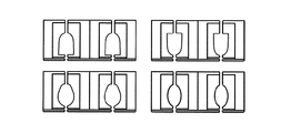
100時間を上回る長時間の試験では、孔の断面形状が角に丸みのある矩形であるプラズマ源(図2)で、断面形状が円形のプラズマ源(図3)よりも、孔の表面でのスパッタリングがかなり多く認められた。 In long-term tests of over 100 hours, a plasma source having a rectangular cross-sectional shape with rounded corners (FIG. 2) was more effective at the surface of the hole than a plasma source with a circular cross-sectional shape (FIG. 3). Quite a lot of sputtering was observed.
実験結果をコンピュータシミュレーションのデータと比較することにより、本発明者らは、中空陰極孔の表面でのスパッタリング量が、数値シミュレーションで決定した場合の中空陰極孔の表面での反応性イオンの吸収に関連していることを見いだした。 By comparing the experimental results with the data of computer simulation, the present inventors found that the amount of sputtering on the surface of the hollow cathode hole was more affected by the absorption of reactive ions on the surface of the hollow cathode hole when determined by numerical simulation. I found something related.
ガス流れとガス放電のシミュレートに用いたシミュレーションソフトウェアは、ドイツのBraunschweigにあるFraunhofer−Institute for Surface Engineering and Thin Films ISTによって開発されたPIC−MCと呼ばれるプログラムである。このソフトウェアでは、ガス流れ、磁場、プラズマのシミュレーションを組み合わせている。 The simulation software used to simulate gas flow and gas discharge is a program called PIC-MC developed by the Fraunhofer-Institute for Surface Engineering and Thin Films IST in Braunschweig, Germany. The software combines gas flow, magnetic field, and plasma simulations.
ガス流れのシミュレーションでは直接シミュレーションモンテカルロ(DSMC)法を使用し、磁場のシミュレーションでは境界要素法(BEM)、プラズマシミュレーションではセル内粒子モンテカルロ法(PIC−MC)を使用する。 The gas flow simulation uses the direct simulation Monte Carlo (DSMC) method, the magnetic field simulation uses the boundary element method (BEM), and the plasma simulation uses the in-cell particle Monte Carlo method (PIC-MC).
中空陰極プラズマ源を横方向に1.016mm厚で切ったスライスである擬似2Dモデルを使用して、シミュレーションを行った。擬似2Dは、スライスの厚みが薄く、周期的な条件が各々の面で横方向に適用されることを意味する。 The simulation was performed using a pseudo 2D model, which is a slice obtained by cutting the hollow cathode plasma source in a width direction at a thickness of 1.016 mm. Pseudo 2D means that the slices are thin and periodic conditions are applied laterally in each plane.
シミュレーション用に、プラズマを形成する多くの異なるガスを使用することができ、以下の例ではアルゴンを使用した。計算時間を制限するために、コーティング原料としてSi2H6を選択し、その可能な反応のうち、以下の2つを選択した。 For the simulation, many different gases that form the plasma can be used, and the following examples used argon. In order to limit the calculation time, Si 2 H 6 was selected as a coating material, and the following two of the possible reactions were selected.
Si2H6+e‐ → Si2H4 ++2H+2e‐(1)
Si2H6+e‐ → SiH3+SiH2+H+e‐(2)
Si 2 H 6 + e − → Si 2 H 4 + + 2H + 2e − (1)
Si 2 H 6 + e − → SiH 3 + SiH 2 + H + e − (2)
水素種は、シミュレーションに含めなかった。 Hydrogen species were not included in the simulation.
入力パラメータの各セットについて、シミュレーションでは、異なる気相種(原子、イオン、分子、電子)が占有する空間全体にわたる、それらの気相種の数と速度に関するデータが得られる。このデータから、密度やフラックスなど、ある値を計算することができる。 For each set of input parameters, the simulation provides data on the number and velocity of different gaseous species (atoms, ions, molecules, electrons) over the space occupied by them. From this data, certain values such as density and flux can be calculated.
ここで、フラックスは、単位面積あたりの気相種の移動量である(単位:mol・m−2・s−1)。 Here, the flux is the movement amount of the gas phase species per unit area (unit: mol · m −2 · s −1 ).
もうひとつの有用な計算に、ある表面に吸収されるフラックスがある。陰極孔材料のある固着係数があれば、その表面に向けられたイオン束から、表面でのイオンの吸収を計算することができる。実験結果をシミュレーションデータと相関させることにより、本発明者らは、シミュレーションモデルに従って、実際のプラズマ源で観察されるデブリの形成、よって孔の表面でのスパッタリングが、電極孔の表面におけるイオン化プラズマ種の吸収レベルに関連していることを見いだした。 Another useful calculation is the flux absorbed on a surface. Given a certain sticking coefficient of the cathode pore material, the ion absorption at the surface can be calculated from the ion flux directed at that surface. By correlating the experimental results with the simulation data, the present inventors have determined that, according to the simulation model, the formation of debris observed in the actual plasma source, and hence the sputtering at the surface of the hole, will result in the ionized plasma species at the surface of the electrode hole. Was found to be related to the level of absorption.
電極孔の表面におけるイオン化プラズマ種の吸収レベルが低ければ、孔でスパッタリングが生じるレベルが低く、デブリの形成が少ないことを意味する。 The lower the level of ionized plasma absorption at the surface of the electrode hole, the lower the level at which sputtering occurs in the hole and the less debris is formed.
別の重要な量として、発生する電子密度がある。電子密度は表面処理またはコーティング効率に大きな影響を与え、電子密度が高ければ表面処理またはコーティング効率も高くなる。 Another important quantity is the electron density generated. The electron density has a great influence on the surface treatment or coating efficiency, and the higher the electron density, the higher the surface treatment or coating efficiency.
本シミュレーションでは、プラズマ源を支持するチャンバ構造から2.54mmの距離に設定したライン上の真空チャンバ内で電子密度を測定し、これを平均した。 In this simulation, the electron density was measured in a vacuum chamber on a line set at a distance of 2.54 mm from the chamber structure supporting the plasma source, and the average was measured.
本発明の一態様では、中空陰極孔の横断面形状が提供される。 In one aspect of the present invention, a cross-sectional shape of a hollow cathode hole is provided.
本発明者らは、驚くべきことに、矩形である孔の断面形状を、少なくとも1つの角に丸みのある矩形または好ましくは4つの角に丸みのある矩形の形状(角に丸みのある矩形の形状)を有する同じ表面領域あるいは、好ましくは4つの角の半径がその幅の半分に等しい角に丸みのある矩形の形状を有するか、最も好ましくは円形の形状を有する同じ表面領域を囲む断面に代えると、陰極孔の表面でのイオン化プラズマ種の吸収レベルが低下することを見いだした。 We have surprisingly found that the cross-sectional shape of a rectangular hole can be reduced to a rectangular shape with at least one rounded corner or preferably a rounded rectangular shape with four rounded corners (a rectangular rounded corner). Shape) or preferably a cross-section surrounding the same surface area having a rectangular shape with rounded corners, with a radius of four corners equal to half its width, or most preferably a circular shape. Alternately, it has been found that the level of absorption of ionized plasma species at the surface of the cathode hole is reduced.
図2は、孔の断面形状が角に丸みのある矩形である、本発明によるプラズマ源の断面図を示す。 FIG. 2 shows a cross-sectional view of a plasma source according to the invention, wherein the cross-sectional shape of the hole is a rectangle with rounded corners.
図3は、孔の断面形状が円形である、本発明によるプラズマ源の断面図を示す。 FIG. 3 shows a cross-sectional view of a plasma source according to the present invention, wherein the cross-sectional shape of the hole is circular.
本発明から逸脱することなく、これらの形状の変形例、特に中間的な形状につながる変形例を作ることができる。特に、楕円形または卵形あるいは、図5に示すような形状の変形例である。 Variations on these shapes, especially those leading to intermediate shapes, can be made without departing from the invention. In particular, it is an elliptical shape, an oval shape, or a modified example of a shape as shown in FIG.
さらに、本発明者らは、孔の断面形状が円形であると、矩形の形状である場合よりも電子密度が改善されることも見いだした。 Further, the present inventors have also found that the electron density is improved when the cross-sectional shape of the hole is circular, as compared with the case where the hole has a rectangular shape.
本発明の一態様では、中空陰極孔の横断面積が提供される。
本発明の一実施形態によれば、孔の断面積は、100mm2〜10000mm2、好ましくは500mm2〜4000mm2である。
In one aspect of the invention, a cross-sectional area of a hollow cathode hole is provided.
According to an embodiment of the present invention, the cross-sectional area of the holes, 100mm 2 ~10000mm 2, preferably 500mm 2 ~4000mm 2.
本発明の別の実施形態によれば、孔の断面積は、100mm2〜1000mm2、好ましくは500mm2〜1000mm2、最も好ましくは500mm2〜750mm2である。本発明者らは、驚くべきことに、孔の断面積が小さいほど、電子密度が大きくなることを見いだした。 According to another embodiment of the present invention, the cross-sectional area of the holes, 100mm 2 ~1000mm 2, it is preferably 500mm 2 ~1000mm 2, most preferably 500mm 2 ~750mm 2. The present inventors have surprisingly found that the smaller the hole cross-sectional area, the higher the electron density.
本発明の別の実施形態によれば、孔の断面積は、1000mm2〜4000mm2、好ましくは1500mm2〜4000mm2、最も好ましくは2000mm2〜4000mm2である。本発明者らは、驚くべきことに、断面積が大きいほど、陰極孔の表面によるイオン化プラズマ種の吸収レベルが低くなることを見いだした。 According to another embodiment of the present invention, the cross-sectional area of the hole, 1000mm 2 ~4000mm 2, it is preferably 1500mm 2 ~4000mm 2, most preferably 2000mm 2 ~4000mm 2. The present inventors have surprisingly found that the larger the cross-sectional area, the lower the level of absorption of ionized plasma species by the surface of the cathode hole.
本発明の別の実施形態によれば、孔の断面積は、750mm2〜1500mm2、好ましくは750mm2〜1250mm2、最も好ましくは1000mm2前後である。本発明者らは、ある中間の断面積で、陰極孔の表面によるイオン化プラズマ種の吸収レベルと電子密度のバランスがとれることを見いだした。 According to another embodiment of the present invention, the cross-sectional area of the holes, 750mm 2 ~1500mm 2, preferably 750mm 2 ~1250mm 2, and most preferably 1000 mm 2 before and after. The present inventors have found that at some intermediate cross-sectional area, the level of absorption of the ionized plasma species by the surface of the cathode hole and the electron density can be balanced.
本発明の一態様では、一方の孔の中心から他方の孔の中心まで測定された中空陰極孔の距離が提供される。孔の中心は、孔が規則的な幾何学形状であれば孔の断面の幾何学中心、不規則な形状であれば孔の重心である。 In one aspect of the invention, a measured distance of the hollow cathode hole from the center of one hole to the center of the other hole is provided. The center of the hole is the geometric center of the cross section of the hole if the hole has a regular geometry, or the center of gravity of the hole if the hole is irregular.
本発明者らは、驚くべきことに、中空陰極孔の距離をある閾値まで増加させると、電子密度の低下とともに、陰極孔の表面によるイオン化プラズマ種の吸収レベルが低下することを見いだした。本発明によれば、孔の距離は、85mm〜160mm、好ましくは100mm〜145mm、最も好ましくは125mm前後である。 The present inventors have surprisingly found that increasing the distance of the hollow cathode hole to a certain threshold reduces the level of absorption of ionized plasma species by the surface of the cathode hole as the electron density decreases. According to the invention, the distance of the holes is between 85 mm and 160 mm, preferably between 100 mm and 145 mm, most preferably around 125 mm.
また、孔の距離が、孔の大きさ、絶縁要件、構造的要件、冷却の要件にも依存することは、当業者には明らかである。 It will be apparent to those skilled in the art that the hole distance also depends on the hole size, insulation requirements, structural requirements, and cooling requirements.
本発明の一態様では、出口ノズルの幅が提供される。 In one aspect of the invention, an outlet nozzle width is provided.
本設計では、出口ノズルは、孔の断面形状の中心を通る垂直線でセンタリングされている。それぞれの孔の断面の中心とその出口ノズルの中心は、孔の断面の中心を通る垂直線と揃っている。しかしながら、本発明から逸脱することなく、出口ノズルの配置と向きを変更および改変してもよい。 In this design, the outlet nozzle is centered on a vertical line passing through the center of the cross-sectional shape of the hole. The center of the cross section of each hole and the center of its outlet nozzle are aligned with a vertical line passing through the center of the cross section of the hole. However, the arrangement and orientation of the outlet nozzle may be changed and modified without departing from the invention.
基本的な設計では、出口ノズルの幅は3.5mm〜5mmの範囲にある。本発明者らは、この幅を広くすると、陰極孔の表面によるイオン化プラズマ種の吸収レベルが低下し、電子密度が増すことを見いだした。ただし、出口ノズルの幅が閾値よりも広くなると、電子密度が大幅に低下する。これはおそらく、孔内の圧力を、有意なプラズマ放電を生じるだけの高いレベルに維持することができないからであろう。 In a basic design, the width of the outlet nozzle ranges from 3.5 mm to 5 mm. The inventors have found that increasing this width reduces the level of absorption of the ionized plasma species by the surface of the cathode hole and increases the electron density. However, when the width of the outlet nozzle is larger than the threshold, the electron density is significantly reduced. This is probably because the pressure in the holes cannot be maintained at a high enough level to produce a significant plasma discharge.
本発明によれば、出口ノズルの幅は、1mm〜25mm、好ましくは3mm〜25mm、より好ましくは8mm〜22mm、より好ましくは8mm〜12mm、最も好ましくは10mm前後である。 According to the invention, the width of the outlet nozzle is between 1 mm and 25 mm, preferably between 3 mm and 25 mm, more preferably between 8 mm and 22 mm, more preferably between 8 mm and 12 mm, most preferably around 10 mm.
本発明の別の実施形態によれば、単一の電源を共通に使用するか、複数の別個の電源を使用して、2つ以上のプラズマ源を組み合わせて表面処理またはコーティング期間を長くすることができる。 According to another embodiment of the invention, a single power supply is commonly used, or multiple separate power supplies are used to combine two or more plasma sources to increase the duration of a surface treatment or coating. Can be.
本発明の別の実施形態によれば、プラズマ源は、例えば表面洗浄、表面更新、表面の活性化など、基材の表面処理に用いられる。基材は、プラズマ源の下を搬送され、プラズマ源の出口ノズル間の真空空間全体に広がるプラズマのイオンと電子に曝露される。 According to another embodiment of the present invention, the plasma source is used for surface treatment of a substrate, for example, surface cleaning, surface renewal, surface activation, and the like. The substrate is transported beneath the plasma source and is exposed to plasma ions and electrons that span the vacuum space between the plasma source outlet nozzles.
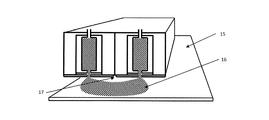
本発明の別の実施形態によれば、プラズマ源は基材をコーティングするために使用される。図4は、プラズマ源の下に搬送され、プラズマ源の2つのノズルの間の真空空間全体に広がるプラズマ16のイオンと電子に曝露される基材15を示す。基材上にコーティングを形成するために、コーティング原料ガスが、ノズル17を介して注入され、プラズマによって活性化される。
According to another embodiment of the present invention, a plasma source is used to coat a substrate. FIG. 4 shows the
<実施例>
実施例1および2
本発明による長さ10cm(プラズマ長)のステンレス鋼中空電極を2つ有するプラズマ源を構築し、以下の条件で100時間より長く動作させた。
<Example>
Examples 1 and 2
A plasma source having two 10 cm (plasma length) stainless steel hollow electrodes according to the present invention was constructed and operated for more than 100 hours under the following conditions.
・電圧の振幅±1200V
・周波数40kHz
・電圧機能:バイポーラ、電圧制御で正弦波
・電力セットポイント20kW、プラズマ源を電力制御モードで動作させる
・プラズマを形成するガスO2;流量は孔長1リニアミリメーターあたり2sccm
・陰極孔の断面積2000mm2
・真空チャンバの圧力:8〜12mTorr
・出口ノズルの幅:3.5mm
・ Voltage amplitude ± 1200V
・ Frequency 40kHz
・ Voltage function: bipolar, sine wave with voltage control ・ Power set point 20 kW, operating plasma source in power control mode ・ Gas O2 forming plasma; flow rate is 2 sccm per linear millimeter of hole length
・ Cross-sectional area of cathode hole 2000mm 2
-Vacuum chamber pressure: 8 to 12 mTorr
・ Width of outlet nozzle: 3.5mm
角に丸みのある矩形と円形の2つの異なる孔の断面形状を比較した。
孔の表面でのスパッタリングは、デブリ粒子の形成につながる。24時間間隔で、ガラス基材上のデブリを回収し、デブリ粒子の数を計数した。以下の表から明らかなように、デブリ粒子の数は、円形の形状よりも角に丸みのある矩形の孔の断面形状で、かなり短時間で増加した。
The cross-sectional shapes of two different holes having a rounded corner and a rectangular shape were compared.
Sputtering at the surface of the holes leads to the formation of debris particles. At 24 hour intervals, debris on the glass substrate was collected and the number of debris particles was counted. As is evident from the table below, the number of debris particles increased in a much shorter time in the cross-sectional shape of the rectangular holes with rounded corners than in the circular shape.

シミュレーションの例
実施例3〜17では、中空陰極プラズマ源をシミュレートした。
Example of Simulation In Examples 3 to 17, hollow cathode plasma sources were simulated.
重要なパラメータの各々について、5つまでの変形例の組を比較した。それぞれの組で、1つの変形例を基準として選択した。変形例ごとに、陰極孔の表面でのイオン化プラズマ種の吸収レベルならびに電子密度を計算した後、この値と基準値との比を求めた。 For each of the important parameters, up to five variant sets were compared. In each set, one variation was selected as a criterion. After calculating the absorption level and the electron density of the ionized plasma species on the surface of the cathode hole for each modification, the ratio between this value and the reference value was determined.
以下のパラメータについては、すべてのシミュレーション例で変更しないようにする。 The following parameters are not changed in all simulation examples.
・電圧の振幅±1200V
・周波数100kHz
・電圧機能:バイポーラ、電圧制御で正弦波
・電力セットポイント25kW/m
・壁温度300K
・原料ガス種Si2H6 流量は孔長1リニアメーターあたり0.13sccm
・プラズマを形成するガスAr 流量は孔長1リニアメーターあたり2.65sccm
・二次電子放出係数が0.1の電極材料(Ag、Cu、Al、Ti、Zn、Feに匹敵)
・真空ポンプをチューニングすることにより、真空チャンバの圧力約10mTorr
・ Voltage amplitude ± 1200V
・ Frequency 100kHz
-Voltage function: Bipolar, sine wave with voltage control-Power set point 25 kW / m
・ Wall temperature 300K
-Flow rate of raw material gas type Si2H6 is 0.13sccm per linear meter with hole length
The flow rate of Ar gas for forming plasma is 2.65 sccm per linear meter of hole length.
-An electrode material with a secondary electron emission coefficient of 0.1 (comparable to Ag, Cu, Al, Ti, Zn, Fe)
By tuning the vacuum pump, the pressure of the vacuum chamber is about 10 mTorr
実施例3〜5 重要なパラメータ:孔の断面形状
矩形、角に丸みのある矩形、円形の3種類の孔の断面形状をシミュレートした。矩形の断面は、幅10mm、高さ50mmとした。角に丸みのある矩形の形状は、4つの角に丸みがあり(角の半径:7mm)、幅約14mm、高さ45mmとした。円形の断面形状は、半径が13mmとした。
Examples 3 to 5 Important parameters: cross-sectional shape of hole The cross-sectional shapes of three types of holes, that is, a rectangle, a rectangle with rounded corners, and a circle were simulated. The rectangular section had a width of 10 mm and a height of 50 mm. The rectangular shape with rounded corners had four rounded corners (corner radius: 7 mm), a width of about 14 mm, and a height of 45 mm. The circular cross section had a radius of 13 mm.
以下のパラメータについては、実施例3〜5で同一とした。 The following parameters were the same in Examples 3 to 5.
−孔の断面積:約500mm2
−出口ノズルの幅:5mm
−孔の距離122mm
The cross-sectional area of the hole: about 500 mm 2
The width of the outlet nozzle: 5 mm
-Hole distance 122 mm
断面形状が矩形から角に丸みのある矩形、円形となっていくにつれて、陰極孔でのイオン化プラズマ種の吸収、よって孔のスパッタリングとデブリの形成が少なくなる。
孔の断面形状が矩形から円形になると、電子密度、よってプロセス効率が高くなる。
As the cross-sectional shape changes from a rectangle to a rectangle with rounded corners and a circle, the absorption of ionized plasma species in the cathode hole, and hence the sputtering of the hole and the formation of debris, decrease.
When the cross-sectional shape of the hole changes from a rectangle to a circle, the electron density and thus the process efficiency increase.
実施例6〜8 重要なパラメータ:孔の断面積
500mm2、1000mm2、2000mm2の3種類の陰極孔の断面積をシミュレートした。
Examples 6-8 important parameters: the cross-sectional area of the cross-sectional area 500mm 2, 1000mm 2, 2000mm 2 three cathode holes of the hole was simulated.
以下のパラメータについては、実施例6〜8で同一とした。 The following parameters were the same in Examples 6 to 8.
−孔の断面形状:円形
−出口ノズルの幅:5mm
−孔の距離122mm
-Cross-sectional shape of hole: circular-Width of outlet nozzle: 5 mm
-Hole distance 122 mm
孔の断面積が大きくなるにつれて、陰極孔でのイオン化プラズマ種の吸収、よって孔のスパッタリングとデブリの形成が少なくなる。 As the cross-sectional area of the holes increases, the absorption of ionized plasma species at the cathode holes, and thus the sputtering of holes and the formation of debris, decreases.
孔の断面積が小さくなるにつれて、電子密度、よってプロセス効率が高くなる。
孔の断面積1000mm2前後では、イオン化種の吸収レベルと電子密度のレベルがバランスする。
As the hole cross-section decreases, the electron density and thus the process efficiency increases.
At a hole cross-sectional area of about 1000 mm 2 , the level of absorption of ionized species and the level of electron density are balanced.
実施例9〜13 重要なパラメータ:孔の距離
168mm、142mm、114mm、104mm、84mmの5種類の孔の距離をシミュレートした。
Examples 9 to 13 Important Parameters: Hole Distance The distances of five types of holes 168 mm, 142 mm, 114 mm, 104 mm and 84 mm were simulated.
以下のパラメータについては、実施例9〜13で同一とした。 The following parameters were the same in Examples 9 to 13.
−孔の断面形状:円形
−孔の断面積:500mm2
−出口ノズルの幅:5mm
- hole cross-sectional shape: circular - sectional area of the holes: 500 mm 2
The width of the outlet nozzle: 5 mm
孔の距離が長くなるにつれて、陰極孔でのイオン化プラズマ種の吸収、よって孔のスパッタリングとデブリの形成が少なくなる。 As the hole distance increases, the absorption of ionized plasma species at the cathode hole, and thus the sputtering of holes and the formation of debris, decreases.
電子密度、よってプロセス効率は、最も高いもの以外、試験したすべての孔の距離で良好なままである。孔の距離が100mm〜145mmの間にあるときに、両方の比の興味深いバランスが得られる。 The electron density, and thus the process efficiency, remains good at the distance of all holes tested except the highest. An interesting balance of both ratios is obtained when the hole distance is between 100 mm and 145 mm.
実施例14〜17 重要なパラメータ:出口ノズルの幅
5mm、10mm、20mm、40mmの4種類のノズルの幅をシミュレーションした。
Examples 14 to 17 Important parameters: width of outlet nozzles The widths of four types of nozzles of 5 mm, 10 mm, 20 mm and 40 mm were simulated.
以下のパラメータについては、実施例9〜13で同一とした。 The following parameters were the same in Examples 9 to 13.
−孔の断面 形状:円形
−孔の断面積:500mm2
−孔の距離:122mm
-Cross section of hole: circular-Cross section of hole: 500 mm 2
-Hole distance: 122mm
出口ノズルの幅が広いほど、陰極孔でのイオン化プラズマ種の吸収、よって孔のスパッタリングとデブリの形成が少なくなる。 The wider the outlet nozzle, the less the ionized plasma species will be absorbed by the cathode hole, and hence the less the hole will sputter and the formation of debris.
出口ノズルの幅が広いほど、電子密度、よってプロセス効率が高くなる。出口ノズルの幅が、例えば40mmと非常に広い場合、真空チャンバと孔の内部の間の圧力差を、安定なプラズマを維持するのに十分なレベルに保つことができず、電子密度レベルが非常に低くなる。 The wider the outlet nozzle, the higher the electron density and thus the process efficiency. If the width of the outlet nozzle is very wide, for example, 40 mm, the pressure difference between the vacuum chamber and the inside of the hole cannot be maintained at a level sufficient to maintain a stable plasma, and the electron density level is very low. Lower.
Claims (11)
細長い孔(4)と、前記プラズマを形成するガス用のガス入口(6)と、基材に向けられた出口ノズル(13)につながるガス出口(7)とを各々有し、正負が交互に入れ替わる電圧を印加する電源と電気的に接続された、第1の電極(1)および第2の電極(2)を備え、
前記陰極が複数あり、複数の前記陰極は互いに実質的に平行であり、
以下のパラメータの値として、
i.前記孔の断面が、矩形、角に丸みのある矩形または円形であるか、これらの形状の中間的な形状であること
ii.前記孔の断面積が、500mm2〜4000mm2であること
iii.前記孔の距離(11)が、85mm〜160mmであること
iv.前記出口ノズルの幅(12)が、1mm〜25mmであること
のうち少なくとも1つが選択される、中空陰極プラズマ源。 A hollow cathode plasma source,
It has an elongated hole (4), a gas inlet (6) for the gas forming the plasma, and a gas outlet (7) leading to an outlet nozzle (13) directed at the substrate, alternating positive and negative. A first electrode (1) and a second electrode (2) electrically connected to a power supply for applying a switching voltage;
A plurality of said cathodes, wherein said plurality of said cathodes are substantially parallel to each other;
As the values of the following parameters:
i. The cross section of the hole is a rectangle, a rectangle with rounded corners or a circle, or an intermediate shape between these shapes; ii. Iii It sectional area of the holes is 500mm 2 ~4000mm 2. The distance (11) of the hole is 85 mm to 160 mm iv. A hollow cathode plasma source, wherein at least one of the outlet nozzles has a width (12) of 1 mm to 25 mm.
前記電極のプラズマを形成するガス入口(6)を介してプラズマを形成するガスを注入し、
前記中空陰極プラズマ源に電圧を印加し、
前記真空チャンバ内で前記プラズマ源によって発生した前記プラズマ(16)に基材(15)を導入することを含む、基材の表面を処理するための方法。 Providing a vacuum chamber having a hollow cathode plasma source according to claim 1;
Injecting a gas forming plasma through a gas inlet (6) forming plasma of said electrode;
Applying a voltage to the hollow cathode plasma source,
A method for treating a surface of a substrate, comprising introducing a substrate (15) into the plasma (16) generated by the plasma source in the vacuum chamber.
前記電極のプラズマを形成するガス入口(6)を介してプラズマを形成するガスを注入し、
前記中空陰極プラズマ源に電圧を印加し、
前記プラズマ源によって発生した前記プラズマに向けてコーティング原料ガスを注入し、
前記真空チャンバ内で前記プラズマ源によって発生した前記プラズマ(16)に基材(15)を導入し、
前記プラズマによって活性化した前記原料ガスからコーティングを施すことを含む、基材をコーティングするための方法。 Providing a vacuum chamber having a hollow cathode plasma source according to claim 1;
Injecting a gas forming plasma through a gas inlet (6) forming plasma of said electrode;
Applying a voltage to the hollow cathode plasma source,
Injecting a coating material gas toward the plasma generated by the plasma source,
Introducing a substrate (15) into said plasma (16) generated by said plasma source in said vacuum chamber;
A method for coating a substrate, comprising applying a coating from the source gas activated by the plasma.
Priority Applications (1)
| Application Number | Priority Date | Filing Date | Title |
|---|---|---|---|
| JP2019212122A JP2020047591A (en) | 2019-11-25 | 2019-11-25 | Hollow cathode plasma source |
Applications Claiming Priority (1)
| Application Number | Priority Date | Filing Date | Title |
|---|---|---|---|
| JP2019212122A JP2020047591A (en) | 2019-11-25 | 2019-11-25 | Hollow cathode plasma source |
Related Parent Applications (1)
| Application Number | Title | Priority Date | Filing Date |
|---|---|---|---|
| JP2017529720A Division JP6710686B2 (en) | 2014-12-05 | 2014-12-05 | Hollow cathode plasma source, substrate treatment method |
Publications (2)
| Publication Number | Publication Date |
|---|---|
| JP2020047591A true JP2020047591A (en) | 2020-03-26 |
| JP2020047591A5 JP2020047591A5 (en) | 2020-06-25 |
Family
ID=69899895
Family Applications (1)
| Application Number | Title | Priority Date | Filing Date |
|---|---|---|---|
| JP2019212122A Pending JP2020047591A (en) | 2019-11-25 | 2019-11-25 | Hollow cathode plasma source |
Country Status (1)
| Country | Link |
|---|---|
| JP (1) | JP2020047591A (en) |
Citations (2)
| Publication number | Priority date | Publication date | Assignee | Title |
|---|---|---|---|---|
| JP2014518947A (en) * | 2011-05-25 | 2014-08-07 | エージーシー グラス ユーロップ | Method for depositing a layer on a glass substrate by low pressure PECVD |
| JP6710686B2 (en) * | 2014-12-05 | 2020-06-17 | エージーシー ガラス ヨーロッパ | Hollow cathode plasma source, substrate treatment method |
-
2019
- 2019-11-25 JP JP2019212122A patent/JP2020047591A/en active Pending
Patent Citations (2)
| Publication number | Priority date | Publication date | Assignee | Title |
|---|---|---|---|---|
| JP2014518947A (en) * | 2011-05-25 | 2014-08-07 | エージーシー グラス ユーロップ | Method for depositing a layer on a glass substrate by low pressure PECVD |
| JP6710686B2 (en) * | 2014-12-05 | 2020-06-17 | エージーシー ガラス ヨーロッパ | Hollow cathode plasma source, substrate treatment method |
Similar Documents
| Publication | Publication Date | Title |
|---|---|---|
| JP6710686B2 (en) | Hollow cathode plasma source, substrate treatment method | |
| US11875976B2 (en) | Plasma source utilizing a macro-particle reduction coating and method of using a plasma source utilizing a macro-particle reduction coating for deposition of thin film coatings and modification of surfaces | |
| US10438778B2 (en) | Plasma source and methods for depositing thin film coatings using plasma enhanced chemical vapor deposition | |
| JP2020047591A (en) | Hollow cathode plasma source |
Legal Events
| Date | Code | Title | Description |
|---|---|---|---|
| A521 | Request for written amendment filed |
Free format text: JAPANESE INTERMEDIATE CODE: A523 Effective date: 20191225 |
|
| A621 | Written request for application examination |
Free format text: JAPANESE INTERMEDIATE CODE: A621 Effective date: 20191225 |
|
| A521 | Request for written amendment filed |
Free format text: JAPANESE INTERMEDIATE CODE: A523 Effective date: 20200428 |
|
| A131 | Notification of reasons for refusal |
Free format text: JAPANESE INTERMEDIATE CODE: A131 Effective date: 20201027 |
|
| A977 | Report on retrieval |
Free format text: JAPANESE INTERMEDIATE CODE: A971007 Effective date: 20201028 |
|
| A521 | Request for written amendment filed |
Free format text: JAPANESE INTERMEDIATE CODE: A523 Effective date: 20210126 |
|
| A02 | Decision of refusal |
Free format text: JAPANESE INTERMEDIATE CODE: A02 Effective date: 20210302 |