JP2017016697A - Single-layer touch-sensitive display - Google Patents
Single-layer touch-sensitive display Download PDFInfo
- Publication number
- JP2017016697A JP2017016697A JP2016186274A JP2016186274A JP2017016697A JP 2017016697 A JP2017016697 A JP 2017016697A JP 2016186274 A JP2016186274 A JP 2016186274A JP 2016186274 A JP2016186274 A JP 2016186274A JP 2017016697 A JP2017016697 A JP 2017016697A
- Authority
- JP
- Japan
- Prior art keywords
- substrate
- patches
- touch sensor
- rows
- patch
- Prior art date
- Legal status (The legal status is an assumption and is not a legal conclusion. Google has not performed a legal analysis and makes no representation as to the accuracy of the status listed.)
- Granted
Links
- 239000002356 single layer Substances 0.000 title claims abstract description 16
- 239000000758 substrate Substances 0.000 claims abstract description 49
- 239000010410 layer Substances 0.000 claims abstract description 17
- 239000004020 conductor Substances 0.000 claims description 18
- 239000003989 dielectric material Substances 0.000 claims description 10
- 239000000463 material Substances 0.000 claims description 3
- 229910052751 metal Inorganic materials 0.000 abstract description 31
- 239000002184 metal Substances 0.000 abstract description 31
- 239000006059 cover glass Substances 0.000 description 6
- 230000005684 electric field Effects 0.000 description 5
- 239000004820 Pressure-sensitive adhesive Substances 0.000 description 4
- 238000004519 manufacturing process Methods 0.000 description 4
- 230000002093 peripheral effect Effects 0.000 description 4
- 229910004298 SiO 2 Inorganic materials 0.000 description 3
- 238000010586 diagram Methods 0.000 description 3
- 229920000620 organic polymer Polymers 0.000 description 3
- 230000009471 action Effects 0.000 description 2
- 239000000853 adhesive Substances 0.000 description 2
- 230000001070 adhesive effect Effects 0.000 description 2
- 239000010408 film Substances 0.000 description 2
- 238000001914 filtration Methods 0.000 description 2
- 230000006870 function Effects 0.000 description 2
- 239000011521 glass Substances 0.000 description 2
- 239000012212 insulator Substances 0.000 description 2
- 238000012986 modification Methods 0.000 description 2
- 230000004048 modification Effects 0.000 description 2
- 230000035945 sensitivity Effects 0.000 description 2
- 241000699670 Mus sp. Species 0.000 description 1
- WYTGDNHDOZPMIW-RCBQFDQVSA-N alstonine Natural products C1=CC2=C3C=CC=CC3=NC2=C2N1C[C@H]1[C@H](C)OC=C(C(=O)OC)[C@H]1C2 WYTGDNHDOZPMIW-RCBQFDQVSA-N 0.000 description 1
- 238000003491 array Methods 0.000 description 1
- 230000008901 benefit Effects 0.000 description 1
- 230000008859 change Effects 0.000 description 1
- 230000000295 complement effect Effects 0.000 description 1
- AMGQUBHHOARCQH-UHFFFAOYSA-N indium;oxotin Chemical compound [In].[Sn]=O AMGQUBHHOARCQH-UHFFFAOYSA-N 0.000 description 1
- 239000011810 insulating material Substances 0.000 description 1
- 229910044991 metal oxide Inorganic materials 0.000 description 1
- 150000004706 metal oxides Chemical class 0.000 description 1
- 150000002739 metals Chemical class 0.000 description 1
- 239000000203 mixture Substances 0.000 description 1
- 230000003287 optical effect Effects 0.000 description 1
- 238000000206 photolithography Methods 0.000 description 1
- 230000001681 protective effect Effects 0.000 description 1
- 230000009467 reduction Effects 0.000 description 1
- 239000004065 semiconductor Substances 0.000 description 1
- 238000004544 sputter deposition Methods 0.000 description 1
- 239000010409 thin film Substances 0.000 description 1
- 239000012780 transparent material Substances 0.000 description 1
Images


Classifications
-
- G—PHYSICS
- G06—COMPUTING; CALCULATING OR COUNTING
- G06F—ELECTRIC DIGITAL DATA PROCESSING
- G06F3/00—Input arrangements for transferring data to be processed into a form capable of being handled by the computer; Output arrangements for transferring data from processing unit to output unit, e.g. interface arrangements
- G06F3/01—Input arrangements or combined input and output arrangements for interaction between user and computer
- G06F3/03—Arrangements for converting the position or the displacement of a member into a coded form
- G06F3/033—Pointing devices displaced or positioned by the user, e.g. mice, trackballs, pens or joysticks; Accessories therefor
- G06F3/0354—Pointing devices displaced or positioned by the user, e.g. mice, trackballs, pens or joysticks; Accessories therefor with detection of 2D relative movements between the device, or an operating part thereof, and a plane or surface, e.g. 2D mice, trackballs, pens or pucks
-
- G—PHYSICS
- G06—COMPUTING; CALCULATING OR COUNTING
- G06F—ELECTRIC DIGITAL DATA PROCESSING
- G06F3/00—Input arrangements for transferring data to be processed into a form capable of being handled by the computer; Output arrangements for transferring data from processing unit to output unit, e.g. interface arrangements
- G06F3/01—Input arrangements or combined input and output arrangements for interaction between user and computer
- G06F3/03—Arrangements for converting the position or the displacement of a member into a coded form
- G06F3/041—Digitisers, e.g. for touch screens or touch pads, characterised by the transducing means
- G06F3/0416—Control or interface arrangements specially adapted for digitisers
- G06F3/04164—Connections between sensors and controllers, e.g. routing lines between electrodes and connection pads
-
- G—PHYSICS
- G06—COMPUTING; CALCULATING OR COUNTING
- G06F—ELECTRIC DIGITAL DATA PROCESSING
- G06F3/00—Input arrangements for transferring data to be processed into a form capable of being handled by the computer; Output arrangements for transferring data from processing unit to output unit, e.g. interface arrangements
- G06F3/01—Input arrangements or combined input and output arrangements for interaction between user and computer
- G06F3/03—Arrangements for converting the position or the displacement of a member into a coded form
- G06F3/041—Digitisers, e.g. for touch screens or touch pads, characterised by the transducing means
- G06F3/0416—Control or interface arrangements specially adapted for digitisers
- G06F3/04166—Details of scanning methods, e.g. sampling time, grouping of sub areas or time sharing with display driving
-
- G—PHYSICS
- G06—COMPUTING; CALCULATING OR COUNTING
- G06F—ELECTRIC DIGITAL DATA PROCESSING
- G06F3/00—Input arrangements for transferring data to be processed into a form capable of being handled by the computer; Output arrangements for transferring data from processing unit to output unit, e.g. interface arrangements
- G06F3/01—Input arrangements or combined input and output arrangements for interaction between user and computer
- G06F3/03—Arrangements for converting the position or the displacement of a member into a coded form
- G06F3/041—Digitisers, e.g. for touch screens or touch pads, characterised by the transducing means
- G06F3/044—Digitisers, e.g. for touch screens or touch pads, characterised by the transducing means by capacitive means
- G06F3/0443—Digitisers, e.g. for touch screens or touch pads, characterised by the transducing means by capacitive means using a single layer of sensing electrodes
-
- G—PHYSICS
- G06—COMPUTING; CALCULATING OR COUNTING
- G06F—ELECTRIC DIGITAL DATA PROCESSING
- G06F3/00—Input arrangements for transferring data to be processed into a form capable of being handled by the computer; Output arrangements for transferring data from processing unit to output unit, e.g. interface arrangements
- G06F3/01—Input arrangements or combined input and output arrangements for interaction between user and computer
- G06F3/03—Arrangements for converting the position or the displacement of a member into a coded form
- G06F3/041—Digitisers, e.g. for touch screens or touch pads, characterised by the transducing means
- G06F3/044—Digitisers, e.g. for touch screens or touch pads, characterised by the transducing means by capacitive means
- G06F3/0446—Digitisers, e.g. for touch screens or touch pads, characterised by the transducing means by capacitive means using a grid-like structure of electrodes in at least two directions, e.g. using row and column electrodes
-
- H—ELECTRICITY
- H03—ELECTRONIC CIRCUITRY
- H03K—PULSE TECHNIQUE
- H03K17/00—Electronic switching or gating, i.e. not by contact-making and –breaking
- H03K17/94—Electronic switching or gating, i.e. not by contact-making and –breaking characterised by the way in which the control signals are generated
- H03K17/96—Touch switches
- H03K17/962—Capacitive touch switches
- H03K17/9622—Capacitive touch switches using a plurality of detectors, e.g. keyboard
-
- G—PHYSICS
- G06—COMPUTING; CALCULATING OR COUNTING
- G06F—ELECTRIC DIGITAL DATA PROCESSING
- G06F2203/00—Indexing scheme relating to G06F3/00 - G06F3/048
- G06F2203/041—Indexing scheme relating to G06F3/041 - G06F3/045
- G06F2203/04103—Manufacturing, i.e. details related to manufacturing processes specially suited for touch sensitive devices
-
- G—PHYSICS
- G06—COMPUTING; CALCULATING OR COUNTING
- G06F—ELECTRIC DIGITAL DATA PROCESSING
- G06F2203/00—Indexing scheme relating to G06F3/00 - G06F3/048
- G06F2203/041—Indexing scheme relating to G06F3/041 - G06F3/045
- G06F2203/04104—Multi-touch detection in digitiser, i.e. details about the simultaneous detection of a plurality of touching locations, e.g. multiple fingers or pen and finger
-
- Y—GENERAL TAGGING OF NEW TECHNOLOGICAL DEVELOPMENTS; GENERAL TAGGING OF CROSS-SECTIONAL TECHNOLOGIES SPANNING OVER SEVERAL SECTIONS OF THE IPC; TECHNICAL SUBJECTS COVERED BY FORMER USPC CROSS-REFERENCE ART COLLECTIONS [XRACs] AND DIGESTS
- Y10—TECHNICAL SUBJECTS COVERED BY FORMER USPC
- Y10T—TECHNICAL SUBJECTS COVERED BY FORMER US CLASSIFICATION
- Y10T29/00—Metal working
- Y10T29/43—Electric condenser making
Abstract
Description
本発明は、一般的に、コンピューティングシステムのための入力装置に係り、より詳細には、基板の片側に製造できる相互キャパシタンスマルチタッチセンサパネルに係る。 The present invention relates generally to input devices for computing systems, and more particularly to a mutual capacitance multi-touch sensor panel that can be fabricated on one side of a substrate.
関連出願の相互参照:本出願は、参考としてここに援用する両方とも“Single-Layer Touch-Sensitive Display”と題する2007年10月4日出願の米国プロビジョナル特許出願第60/977,621号及び2008年2月27日出願の米国特許出願第12/038,760号の優先権を主張する。 Cross-reference to related applications: This application is a US Provisional Patent Application Nos. 60 / 977,621 and 2008 filed Oct. 4, 2007, both of which are hereby incorporated by reference as “Single-Layer Touch-Sensitive Display”. Claims priority of US patent application Ser. No. 12 / 038,760, filed Feb. 27, 1980.
コンピューティングシステムの動作を行うために、現在では、ボタン又はキー、マウス、トラックボール、タッチ感知パネル、ジョイスティック、タッチスクリーン、等の多数の形式の入力装置を利用することができる。特に、タッチスクリーンは、操作が容易で、多様性があり、価格も低下しているので、益々普及してきている。タッチスクリーンは、タッチ感知面をもつ透明パネルであるタッチセンサパネルを含むことができる。タッチセンサパネルは、タッチ感知面がディスプレイスクリーンのビューエリアをカバーするように、ディスプレイスクリーンの前部に配置することができる。タッチスクリーンは、ユーザが指又はスタイラスでディスプレイスクリーンにタッチするだけで選択を行い且つカーソルを移動できるようにする。一般的に、タッチスクリーンは、ディスプレイスクリーンへのタッチ及びタッチの位置を認識することができ、そしてコンピューティングシステムは、タッチを解釈し、その後、タッチ事象に基づきアクションを遂行することができる。 Numerous types of input devices such as buttons or keys, mice, trackballs, touch sensitive panels, joysticks, touch screens, and the like are currently available for performing computing system operations. In particular, touch screens are becoming more and more popular because they are easy to operate, have variety, and have a lower price. The touch screen may include a touch sensor panel that is a transparent panel having a touch-sensitive surface. The touch sensor panel can be placed at the front of the display screen such that the touch-sensitive surface covers the view area of the display screen. The touch screen allows the user to make selections and move the cursor simply by touching the display screen with a finger or stylus. In general, the touch screen can recognize the touch on the display screen and the location of the touch, and the computing system can interpret the touch and then perform an action based on the touch event.
タッチセンサパネルは、複数のドライブ線(例えば、行)が複数のセンス線(例えば、列)に交差することによって形成されるピクセルのアレイとして具現化することができ、ドライブ線及びセンス線は、誘電体材料により分離される。このようなタッチセンサパネルの例が、参考としてここに援用する2007年1月3日出願の“Double-Sided Touch Sensitive Panel and Flex Circuit Bonding”と題する同時係争中の米国特許出願第11/650,049号に説明されている。しかしながら、ドライブ線及びセンス線が単一基板の下面及び上面に形成されたタッチ感知パネルは、製造経費が高くなる。この付加的な経費の1つの理由は、ガラス基板の両側で薄膜処理ステップを遂行しなければならず、処理された側には、他側を処理する間に保護手段が必要になることである。別の理由は、基板の両側に接続するのに必要な可撓性回路の製造及び接合のコストである。 The touch sensor panel can be embodied as an array of pixels formed by a plurality of drive lines (eg, rows) intersecting a plurality of sense lines (eg, columns), where the drive lines and sense lines are Separated by dielectric material. An example of such a touch sensor panel is described in co-pending US patent application Ser. No. 11/650, entitled “Double-Sided Touch Sensitive Panel and Flex Circuit Bonding,” filed Jan. 3, 2007, incorporated herein by reference. No. 049. However, the touch sensing panel in which the drive lines and the sense lines are formed on the lower surface and the upper surface of the single substrate has a high manufacturing cost. One reason for this additional cost is that thin film processing steps must be performed on both sides of the glass substrate, and the processed side requires protective measures while processing the other side. . Another reason is the cost of manufacturing and bonding the flexible circuit required to connect to both sides of the substrate.
本発明は、単一又は複数タッチ事象(1つ又は複数の指或いは他の物体がタッチ感知面の個別の位置にほぼ同時にタッチすること)を検出するために基板の片側に製造された同一平面単層タッチセンサを有する実質的に透明なタッチセンサパネルに係る。同じ基板の両側に実質的に透明なドライブ線及びセンス線を製造する必要性を回避するため、本発明の実施形態は、基板の同じ側の同一平面単層にドライブ線及びセンス線を形成することができる。ドライブ線及びセンス線は、第1方向には列状パターンとして、又、第2方向にはパッチとして製造することができ、第1方向における各列状パターンは、タッチセンサパネルの境界エリアにおいて個別の金属トレースに接続され、そして第2方向の複数の行の各々における全てのパッチは、タッチセンサパネルの境界エリアにおいて個別の金属トレース(又は他の導電性材料)を使用して一緒に接続される。境界エリアにおける金属トレースは、パッチ及び列と同じ基板側に形成されるが、誘電体層によりパッチ及び列状パターンから分離することができる。金属トレースは、パッチ及び列状パターンの両方を基板の同じ短いエッジへ引き回すことができ、小さな可撓性回路を基板の片側のみにおいて小さなエリアに接合できるようにする。 The present invention is a coplanar fabricated on one side of a substrate to detect single or multiple touch events (one or more fingers or other objects touching discrete locations on the touch sensitive surface at about the same time). A substantially transparent touch sensor panel having a single layer touch sensor. In order to avoid the need to fabricate substantially transparent drive and sense lines on both sides of the same substrate, embodiments of the present invention form drive and sense lines in the same planar monolayer on the same side of the substrate. be able to. The drive lines and sense lines can be manufactured as columnar patterns in the first direction and as patches in the second direction, and each columnar pattern in the first direction is individually separated in the boundary area of the touch sensor panel. And all patches in each of the plurality of rows in the second direction are connected together using separate metal traces (or other conductive material) in the border area of the touch sensor panel. The The metal traces in the boundary area are formed on the same substrate side as the patches and rows, but can be separated from the patches and rows pattern by a dielectric layer. The metal traces can route both the patch and the row pattern to the same short edge of the substrate, allowing a small flexible circuit to be joined to a small area on only one side of the substrate.
好ましい実施形態の以下の説明において、本発明を実施できる特定の実施形態を例示した添付図面を参照する。本発明の範囲から逸脱せずに、他の実施形態も使用できると共に、構造上の変更も可能であることを理解されたい。 In the following description of the preferred embodiments, reference will be made to the accompanying drawings, which illustrate specific embodiments in which the invention may be practiced. It should be understood that other embodiments may be used and structural changes may be made without departing from the scope of the invention.
本発明は、単一又は複数タッチ事象(1つ又は複数の指或いは他の物体がタッチ感知面の個別の位置にほぼ同時にタッチすること)を検出するために基板の片側に製造された同一平面単層タッチセンサを有する実質的に透明なタッチセンサパネルに係る。同じ基板の両側に実質的に透明なドライブ線及びセンス線を製造する必要性を回避するため、本発明の実施形態は、基板の同じ側の同一平面単層にドライブ線及びセンス線を形成することができる。ドライブ線及びセンス線は、第1方向には列状パターンとして、又、第2方向にはパッチとして製造することができ、第1方向における各列状パターンは、タッチセンサパネルの境界エリアにおいて個別の金属トレースに接続され、そして第2方向の複数の行の各々における全てのパッチは、タッチセンサパネルの境界エリアにおいて個別の金属トレース(又は他の導電性材料)を使用して一緒に接続される。境界エリアにおける金属トレースは、パッチ及び列と同じ基板の側に形成されるが、誘電体層によりパッチ及び列状パターンから分離することができる。金属トレースは、パッチ及び列状パターンの両方を基板の同じ短い縁へ引き回すことができ、小さな可撓性回路を基板の片側のみにおいて小さなエリアに接合できるようにする。 The present invention is a coplanar fabricated on one side of a substrate to detect single or multiple touch events (one or more fingers or other objects touching discrete locations on the touch sensitive surface at about the same time). A substantially transparent touch sensor panel having a single layer touch sensor. In order to avoid the need to fabricate substantially transparent drive and sense lines on both sides of the same substrate, embodiments of the present invention form drive and sense lines in the same planar monolayer on the same side of the substrate. be able to. The drive lines and sense lines can be manufactured as columnar patterns in the first direction and as patches in the second direction, and each columnar pattern in the first direction is individually separated in the boundary area of the touch sensor panel. And all patches in each of the plurality of rows in the second direction are connected together using separate metal traces (or other conductive material) in the border area of the touch sensor panel. The The metal traces in the boundary area are formed on the same substrate side as the patches and rows, but can be separated from the patches and rows pattern by a dielectric layer. The metal traces can route both the patch and the row pattern to the same short edge of the substrate, allowing a small flexible circuit to be joined to a small area on only one side of the substrate.
本発明の幾つかの実施形態を、ここで、相互キャパシタンスマルチタッチセンサパネルに関して説明するが、本発明の実施形態は、これに限定されず、自己キャパシタンスセンサパネル及び単一タッチセンサパネルにも適用できることを理解されたい。更に、センサパネルにおけるタッチセンサは、ここでは、行及び列を有するタッチセンサの直交アレイに関して説明するが、本発明の実施形態は、直交アレイに限定されず、一般的に、対角、同心円、三次元及びランダム方向を含めて、いかなる数の次元及び方向に配列されるタッチセンサにも適用することができる。 Although some embodiments of the present invention will now be described with respect to a mutual capacitance multi-touch sensor panel, embodiments of the present invention are not so limited and apply to self-capacitance sensor panels and single touch sensor panels. Please understand that you can. Furthermore, although the touch sensors in the sensor panel are described herein with respect to an orthogonal array of touch sensors having rows and columns, embodiments of the present invention are not limited to orthogonal arrays, and are generally diagonal, concentric, It can be applied to touch sensors arranged in any number of dimensions and directions, including three-dimensional and random directions.
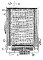
図1Aは、本発明の実施形態により基板の片側に製造された同一平面単層タッチセンサを有する実質的に透明のタッチセンサパネル100を例示する部分図である。図1Aの実施例において、8列(aからhで示す)及び6行(1から6で示す)を有するタッチセンサパネル100が示されているが、いかなる数の列及び行も使用できることを理解されたい。列aからhは、一般的に、形状が柱状であるが、図1Aの実施例では、各列の片側が、食い違ったエッジ、及び各列に個別の区分を生成するように設計されたノッチを含む。行1から6の各々は、複数の個別のパッチ又はパッドで形成することができ、各パッチは、そのパッチと同じ材料のトレースであって、タッチセンサパネル100の境界エリアへ引き回されて、特定行における全てのパッチを、境界エリアに延びる金属トレース(図1Aには示さず)を経て一緒に接続できるようにするためのトレースを含む。前記金属トレースは、タッチセンサパネル100の片側の小さなエリアへ引き回して可撓性回路102へ接続することができる。図1Aの実施例に示されたように、行を形成するパッチは、一般的にピラミッド状の構成で配列することができる。図1Aにおいて、例えば、列aとbとの間の行1から3に対するパッチは、逆ピラミッド構成で配列され、一方、列aとbとの間の行4から6に対するパッチは、直立したピラミッド構成で配列される。
FIG. 1A is a partial view illustrating a substantially transparent
図1Aの列及びパッチは、導電性材料の同一平面単層に形成することができる。タッチスクリーン実施形態では、導電性材料は、単層インジウムスズ酸化物(SITO)のような実質的に透明な材料であるが、他の材料も使用できる。SITTO層は、カバーガラスの背面又は個別基板の頂面に形成することができる。SITOは、ここでは、開示を簡単にするために取り上げるが、本発明の実施形態では、他の導電性材料も使用できることを理解されたい。 The rows and patches of FIG. 1A can be formed in a coplanar monolayer of conductive material. In touch screen embodiments, the conductive material is a substantially transparent material such as single layer indium tin oxide (SITO), although other materials can be used. The SITTO layer can be formed on the back surface of the cover glass or on the top surface of the individual substrate. Although SITO is taken here for ease of disclosure, it should be understood that other conductive materials may be used in embodiments of the present invention.
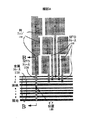
図1Bは、本発明の実施形態によりタッチセンサパネルの境界エリアに延びる金属トレース104及び106を含む実質的に透明なタッチセンサパネル100を例示する部分図である。図1Bの境界エリアは、明瞭化のために拡大されている。各列aからhは、ビア(図1Bには示さず)を経て金属トレースに列を接続できるようにするSITOトレース108を含むことができる。各列の片側は、食い違ったエッジ114、及び各列に個別の区分を生成するように設計されたノッチ116を含む。各行のパッチ1から6は、ビア(図1Bには示さず)を経て金属トレースにパッチを接続できるようにするSITOトレース110を含むことができる。このSITOトレース110は、特定行の各パッチを互いに自己接続できるようにする。金属トラック104及び106は、全て、同じ層に形成されるので、それらを全て同じ可撓性回路102へ引き回すことができる。
FIG. 1B is a partial view illustrating a substantially transparent
タッチセンサパネル100が相互キャパシタンスのタッチセンサパネルとして動作する場合には、列a−h又は行1−6は、1つ以上の刺激信号で駆動することができ、そして隣接する列エリアと行パッチとの間にフリンジ電界線を形成することができる。図1Bでは、説明上、列aと行パッチ1との(a−1)間の電界線112しか示されていないが、どんな列又は行が刺激されるかに基づいて、他の隣接列と行パッチとの間(例えば、a−2、b−4、g−5、等)に電界線を形成できることも理解されたい。従って、各列−行パッチ対(例えば、a−1、a−2、b−4、g−5、等)は、ドライブ電極からセンス電極へ電荷を結合できるところの2電極ピクセル又はセンサを表すことを理解されたい。これらピクセルの1つに指を接触させると、タッチセンサパネルのカバーを越えて延びるフリンジ電界線の幾つかが指で阻止され、センス電極へ結合される電荷の量が減少される。結合される電荷の量のこのような減少は、タッチの結果生じる「映像」を決定する部分として検出することができる。図1Bに示すような相互キャパシタンスのタッチセンサパネル設計では、個別の基準接地部が必要とされず、従って、基板の裏側又は個別の基板上の第2層が必要とされない。
When
又、タッチセンサパネル100は、自己キャパシタンスのタッチセンサパネルとして動作することもできる。このような実施形態では、基準接地平面を、基板の裏側に形成するか、パッチ及び列と同じ側に誘電体によりパッチ及び列から分離して形成するか、或いは個別の基板上に形成することができる。自己キャパシタンスのタッチセンサパネルでは、各ピクセル又はセンサが、基準接地部に対して、指の存在により変化する自己キャパシタンスを有する。自己キャパシタンスの実施形態では、列a−hの自己キャパシタンスは、独立して感知することができ、又、行1−6の自己キャパシタンスも、独立して感知することができる。
The
図1Cは、本発明の実施形態によりタッチセンサパネルの境界エリアにおいて金属トレースに列及び行パッチを接続するところを例示する図である。図1Cは、図1Bに示された「細部A」を表し、SITOトレース108及び110を通して金属トレース118に接続された列「a」及び行パッチ4−6を示す。SITOトレース108及び110は、金属トレース118から誘電体材料により分離されているので、誘電体材料に形成されたビア120は、SITOトレースを金属トレースに接続できるようにする。
FIG. 1C is a diagram illustrating connecting column and row patches to metal traces in a border area of a touch sensor panel according to an embodiment of the present invention. FIG. 1C represents “detail A” shown in FIG. 1B and shows column “a” and row patches 4-6 connected to
図2Aは、タッチセンサパネル200の断面図で、本発明の実施形態により誘電体材料222のビア220を通して接続されたSITOトレース208及び金属トレース218を示している。図2Aは、図1Cに示されたB−B断面を表す。
FIG. 2A is a cross-sectional view of touch sensor panel 200 showing
図2Bは、本発明の実施形態による図2Aに示された断面の拡大図である。図2Bは、SITOトレース208が最大約155オーム/平方の抵抗率を有する一実施形態を例示する。一実施形態では、誘電体222は、約1500Åの無機SiO2であり、これは、高温で処理することができ、それ故、SITO層を高いクオリティでスパッタすることができる。別の実施形態では、誘電体222は、約3.0ミクロンの有機ポリマーである。1500Åの無機SiO2は、(SITOトレース208と金属トレース218との間の)クロスオーバーキャパシタンスが問題とならないような充分に小さなタッチセンサパネルに使用することができる。
2B is an enlarged view of the cross section shown in FIG. 2A according to an embodiment of the present invention. FIG. 2B illustrates one embodiment where the
(対角寸法が約3.5”以上の)大きなタッチセンサパネルの場合には、クロスオーバーキャパシタンスが問題となり、部分的にしか補償できないエラー信号を発生する。従って、大きなタッチセンサパネルの場合には、約3.0ミクロンの有機ポリマーのような低誘電率の厚い誘電体層222を使用して、クロスオーバーキャパシタンスを下げることができる。しかしながら、厚い誘電体層の使用は、SITO層を低い温度で強制的にスパッタさせ、低い光学的クオリティ及び高い抵抗率を招く。
In the case of a large touch sensor panel (diagonal dimension of about 3.5 ″ or more), the crossover capacitance becomes a problem and generates an error signal that can only be partially compensated. Can reduce the crossover capacitance using a low dielectric constant thick
再び、図1Cの実施例を参照すれば、列エッジ114及び行パッチ4−6は、x次元において食い違わせることができる。というのは、行パッチ4及び5を接続するSITOトレース110のためのスペースを作らねばならないからである。(図1Cの実施例における行パッチ4は、実際には、2つのパッチを一緒に貼り付けたものであることを理解されたい。)最適なタッチ感度を得るため、ピクセルa−6、a−5及びa−4における電極の面積をバランスさせることが望まれる。しかしながら、列「a」がまっすぐ保持される場合は、行パッチ6を行パッチ5又は6より細くすることができ、ピクセルa−6の電極間にアンバランスが生じることになる。
Again referring to the example of FIG. 1C, the column edges 114 and the row patches 4-6 can be confused in the x dimension. This is because a space for the
図3は、本発明の実施形態による列及び隣接行パッチの上面図である。タッチ感知回路の範囲内に留まる比較的均一なz方向タッチ感度を生じさせるために、ピクセルa−4、a−5及びa−6の相互キャパシタンス特性を比較的一定にすることが一般に望まれる。従って、列面積a4、a5及びa6は、行パッチ面積4、5及び6とほぼ同じでなければならない。これを達成するために、列区分a4及びa5、並びに行パッチ4及び5は、列区分a6及び行パッチ6に比してy方向に収縮させて、列セグメントa4の面積を列セグメントa5及びa6の面積に一致させることができる。換言すれば、ピクセルa4−4は、狭くて背の高いピクセルa6−6より広くて短いものである。
FIG. 3 is a top view of column and adjacent row patches according to an embodiment of the present invention. It is generally desirable to make the mutual capacitance characteristics of pixels a-4, a-5 and a-6 relatively constant in order to produce a relatively uniform z-direction touch sensitivity that stays within the touch sensing circuitry. Thus, the column areas a 4 , a 5 and a 6 must be approximately the same as the
以上に述べた図から、生の空間的感度は、若干歪があることが明らかである。換言すれば、ピクセル又はセンサは、x方向に若干スキューし又は不整列になるので、ピクセルa−6における最大タッチ事象(例えば、ピクセルa−6の真上に置いた指)のx座標は、例えば、ピクセルa−4における最大タッチ事象のx座標とは若干異なることがある。従って、本発明の実施形態では、この不整列をソフトウェアアルゴリズムでワープ補正(de-warp)し、ピクセルを再マップすると共に、歪を除去することができる。 From the figures described above, it is clear that the raw spatial sensitivity is slightly distorted. In other words, because the pixel or sensor is slightly skewed or misaligned in the x direction, the x coordinate of the maximum touch event at pixel a-6 (eg, the finger placed directly above pixel a-6) is For example, the x coordinate of the maximum touch event at pixel a-4 may be slightly different. Thus, in an embodiment of the present invention, this misalignment can be de-warped with a software algorithm to remap the pixels and remove distortion.
典型的なタッチパネルグリッド寸法は、5.0mm中心で配列されたピクセルを有するが、タッチセンサパネルにおける電気的接続の合計数を減少するためには、例えば、約6.0mm中心をもつより分散したグリッドが望まれる。しかしながら、センサパターンを分散すると、タッチの読みを誤ることがある。 A typical touch panel grid size has pixels arranged at 5.0 mm centers, but to reduce the total number of electrical connections in the touch sensor panel, for example, more dispersed with about 6.0 mm centers. A grid is desired. However, when sensor patterns are distributed, touch reading may be erroneous.
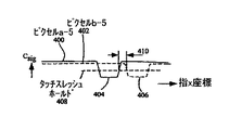
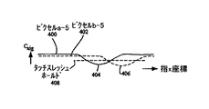
図4Aは、広い間隔を有する単一行内の2つの隣接ピクセルa−5及びb−5に対して、指タッチのx座標と、ピクセルに見られる相互キャパシタンスとをプロットしたものである。図4Aにおいて、プロット400は、指タッチが左から右へ連続的に移動するときにピクセルa−5に見られる相互キャパシタンスを表し、そしてプロット402は、指タッチが左から右へ連続的に移動するときにピクセルb−5に見られる相互キャパシタンスを表す。予期されるように、指タッチがピクセルa−5の真上を通過するときにピクセルa−5に相互キャパシタンスの降下404が見られ、そして指タッチがピクセルb−5の真上を通過するときにピクセルb−5に相互キャパシタンスの降下406が見られる。線408がタッチ事象を検出するためのスレッシュホールドを表す場合に、図4Aは、タッチセンサパネルの表面から指が持ち上げられなくても、指が瞬間的に表面から持ち上げられたことが410に誤って現れることを示している。この位置410は、2つの分散したピクセルの間のほぼ中間の点を表すことができる。
FIG. 4A plots the x coordinate of a finger touch and the mutual capacitance seen at the pixel for two adjacent pixels a-5 and b-5 in a single row with wide spacing. In FIG. 4A,
図4Bは、広い間隔を有する単一行内の2つの隣接ピクセルa−5及びb−5に対して、指タッチのx座標と、ピクセルに見られる相互キャパシタンスとをプロットしたものであって、本発明の実施形態により空間的な補間がなされる場合を示す。予期されるように、指タッチがピクセルa−5の真上を通過するときにピクセルa−5に相互キャパシタンスの降下404が見られ、そして指タッチがピクセルb−5の真上を通過するときにピクセルb−5に相互キャパシタンスの降下406が見られる。しかしながら、相互キャパシタンス値の上昇及び下降は、図4Aの場合より徐々に生じることに注意されたい。線408がタッチ事象を検出するためのスレッシュホールドを表す場合に、図4Bは、指がピクセルa−5及びb−5上を左から右へ移動するときに、タッチ事象が常にピクセルa−5又はb−5で検出されることを示す。換言すれば、タッチ事象のこの「ぼけ」は、偽の非タッチ読みが現れるのを防止する上で役立つ。
FIG. 4B is a plot of the x coordinate of finger touch and the mutual capacitance seen in a pixel for two adjacent pixels a-5 and b-5 in a single row with wide spacing. A case where spatial interpolation is performed according to an embodiment of the invention will be described. As expected, a
本発明の一実施形態において、図4Bに示した空間的なぼけ又はフィルタリングの一部又は全部を生成するために、タッチセンサパネルのためのカバーガラスの厚みを増加することができる。 In one embodiment of the present invention, the thickness of the cover glass for the touch sensor panel can be increased to generate some or all of the spatial blurring or filtering shown in FIG. 4B.
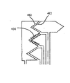
図4Cは、本発明の実施形態により大きなピクセル間隔に有用な列及び隣接行パッチパターンを例示する上面図である。図4Cは、鋸歯状電極エッジ412が、x方向に延びるピクセル内に使用された実施形態を例示している。鋸歯状電極エッジは、フリンジ電界線414を広いエリアにわたりx方向に存在させて、x方向に大きな距離にわたり同じピクセルによってタッチ事象を検出できるようにする。図4Cの鋸歯状構成は例示に過ぎず、又、曲がりくねったエッジのような他の構成等も使用できることを理解されたい。これらの構成は、タッチパターンを更に軟化させ、図4Bに示す隣接ピクセル間に付加的な空間的フィルタリング及び補間を生成することができる。
FIG. 4C is a top view illustrating column and adjacent row patch patterns useful for large pixel spacings according to embodiments of the present invention. FIG. 4C illustrates an embodiment in which serrated electrode edges 412 are used in pixels extending in the x direction. The serrated electrode edge allows
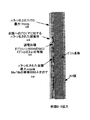
図5は、本発明の実施形態によりカバーガラスに接合されたタッチセンサパネル基板上のSITOの積層体を例示する図である。この積層体は、ガラスで形成できるタッチセンサパネル基板500を備え、その片側には反射防止(AR)膜510を形成することができ、そしてその他側には金属502を堆積及びパターン化して、境界エリアにバス線を形成することができる。金属502は、抵抗率が最大0.8Ω/平方である。次いで、基板500及び金属502の上に絶縁層504を堆積することができる。絶縁層は、例えば、厚みが1500ÅのSiO2であるか、又は3μの有機ポリマーである。ホトリソグラフィーを使用して、絶縁材504にビア506を形成することができ、そして絶縁材及び金属502の頂部に導電性材料508を堆積しパターン化することができる。抵抗率が最大155Ω/平方のITOのような透明な導電性材料から形成できる導電性材料の単一層508は、多層設計より透明度が高く、製造容易でもある。非等方性導電性膜(ACF)のような接着剤514を使用して、導電性材料508及び金属502に可撓性回路512を接合することができる。次いで、感圧接着剤(PSA)のような接着剤518を使用してカバーガラス516及びブラックマスク520にサブアッセンブリ全体を接合することができる。
FIG. 5 is a diagram illustrating a laminate of SITO on a touch sensor panel substrate bonded to a cover glass according to an embodiment of the present invention. The laminate includes a touch
別の実施形態では、上述した金属、絶縁材、導電性材料をカバーガラスの背面に直接形成することができる。 In another embodiment, the metals, insulating materials, and conductive materials described above can be formed directly on the back surface of the cover glass.
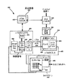
図6は、本発明の実施形態による前記タッチセンサパネルと共に動作可能なコンピューティングシステム600を例示する図である。タッチセンサパネル624及びディスプレイ装置640(例えば、LCDモジュール)を含むことのできるタッチスクリーン642は、センサパネルに一体的に形成されたコネクタを通して、又は可撓性回路を使用して、コンピューティングシステム600内の他のコンポーネントに接続することができる。コンピューティングシステム600は、1つ以上のパネルプロセッサ602及び周辺機器604、並びにパネルサブシステム606を備えることができる。1つ以上のプロセッサ602は、例えば、ARM968プロセッサ、又は同様の機能及び能力を伴う他のプロセッサを含むことができる。しかしながら、他の実施形態では、パネルプロセッサの機能は、状態マシンのような専用ロジックによって具現化することもできる。周辺機器604は、これに限定されないが、ランダムアクセスメモリ(RAM)、又は他の形式のメモリ又は記憶装置、ウオッチドッグタイマー、等を含むことができる。
FIG. 6 is a diagram illustrating a
パネルサブシステム606は、これに限定されないが、1つ以上のアナログチャンネル608、チャンネルスキャンロジック610及びドライバロジック614を含むことができる。チャンネルスキャンロジック610は、RAM612にアクセスし、アナログチャンネルからデータを自律的に読み出し、そしてアナログチャンネルのための制御を与える。この制御は、タッチセンサパネル624のセンス線をアナログチャンネル608へマルチプレクスし、さもなければ、接続することを含む。更に、チャンネルスキャンロジック610は、タッチセンサパネル624のドライブ線に選択的に印加されるドライバロジック及び刺激信号を制御することができる。ある実施形態では、パネルサブシステム606、パネルプロセッサ602及び周辺機器604を、単一の特定用途向け集積回路(ASIC)へ一体化することができる。
ドライバロジック614は、複数のパネルサブシステム出力616を発生し、そして高電圧ドライバ618を駆動する専有インターフェイスを与えることができる。高電圧ドライバ618は、低電圧レベル(例えば、相補的金属酸化物半導体(CMOS)レベル)から高電圧レベルへのレベルシフトを与え、ノイズ減少目的で良好な信号対雑音比(S/N)を与えることができる。パネルサブシステム出力616は、デコーダ620及びレベルシフタ/ドライバ638へ送ることができ、これらは、1つ以上の高電圧ドライバ出力を、専有インターフェイスを通して1つ以上のパネル行又はドライブ線入力622へ選択的に接続し、そして高電圧ドライバ618内の少数の高電圧ドライバ回路を使用できるようにする。各パネル行入力622は、タッチセンサパネル624内の1つ以上のドライブ線を駆動することができる。ある実施形態では、高電圧ドライバ618及びデコーダ620を単一のASICへ一体化することができる。しかしながら、他の実施形態では、高電圧ドライバ618及びデコーダ620をドライバロジック614へ一体化することができ、そして更に別の実施形態では、高電圧ドライバ618及びデコーダ620を完全に排除することもできる。
Driver logic 614 can generate a plurality of panel subsystem outputs 616 and provide a proprietary interface to drive
又、コンピューティングシステム600は、パネルプロセッサ602から出力を受け取りそしてその出力に基づいてアクションを遂行するためのホストプロセッサ628も備えることができ、そのアクションは、これに限定されないが、カーソル又はポインタのようなオブジェクトを移動し、スクロール又はパンを行い、制御設定を調整し、ファイル又はドキュメントをオープンし、メニューを見、選択を行い、インストラクションを実行し、ホスト装置に接続された周辺機器を操作し、電話コールに応答し、電話コールを発信し、電話コールを終了し、音量又は音声設定を変更し、住所、頻繁にダイヤルされる番号、受けたコール、逃したコールのような電話通信に関連した情報を記憶し、コンピュータ又はコンピュータネットワークにログし、許可された個人がコンピュータ又はコンピュータネットワークの制限エリアにアクセスするのを許し、コンピュータデスクトップのユーザの好みの構成に関連したユーザプロフィールをロードし、ウェブコンテンツへのアクセスを許し、特定プログラムを起動し、メッセージを暗号化又は解読し、等々を含むことができる。又、ホストプロセッサ628は、パネル処理に関係のない付加的な機能も遂行できると共に、プログラム記憶装置632と、装置のユーザにユーザインターフェイス(UI)を与えるためのLCDのようなディスプレイ装置640とに接続することができる。
The
上述したタッチセンサパネルは、低コストで、製造し易く且つ既存の機械的制御アウトライン(同じ物理的外被)に適合するスペース効率の良いタッチセンサパネル及びUIを形成するように図6のシステムに好都合に使用することができる。 The touch sensor panel described above is a low cost, easy to manufacture and space efficient touch sensor panel and UI that is compatible with existing mechanical control outlines (same physical envelope). Can be used conveniently.
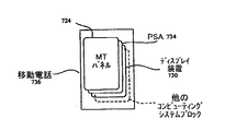
図7Aは、本発明の実施形態による上述したタッチセンサパネル724及びディスプレイ装置730の積層体(任意であるがPSA734を使用して一緒に接合された)並びにコンピューティングシステムを含むことのできる移動電話736を例示する。図7Bは、本発明の実施形態による上述したタッチセンサパネル724及びディスプレイ装置730の積層体(任意であるがPSA734を使用して一緒に接合された)並びにコンピューティングシステムを含むことのできるデジタルオーディオ/ビデオプレーヤ740を例示する。図7A及び7Bの移動電話及びデジタルオーディオ/ビデオプレーヤは、好都合にも、上述したタッチセンサパネルから利益を得ることができる。というのは、タッチセンサパネルは、これら装置を小型で且つ安価なものにすることができ、これは、消費者の希望及び商業的成功に顕著な作用を及ぼす重要な消費者ファクタだからである。
FIG. 7A illustrates a mobile phone that can include a stack of
以上、添付図面を参照して、本発明の実施形態を詳細に説明したが、当業者であれば、種々の変更や修正が明らかであろう。このような変更や修正は、特許請求の範囲で規定される本発明の実施形態の範囲内に包含されると理解される。 Although the embodiments of the present invention have been described in detail with reference to the accompanying drawings, various changes and modifications will be apparent to those skilled in the art. Such changes and modifications are to be understood as being included within the scope of embodiments of the present invention as defined by the appended claims.
100:タッチセンサパネル
102:可撓性回路
104、106:金属トレース
108、110:SITOトレース
112:電界線
114:食い違ったエッジ
116:ノッチ
120:ビア
200:タッチセンサパネル
208:SITOトレース
218:金属トレース
220:ビア
222:誘電体材料
404、406:相互キャパシタンス
412:鋸歯電極エッジ
414:フリンジ電界線
100: Touch sensor panel 102: Flexible circuit 104, 106: Metal trace 108, 110: SITO trace 112: Electric field line 114: Misaligned edge 116: Notch 120: Via 200: Touch sensor panel 208: SITO trace 218: Metal Trace 220: Via 222:
Claims (20)
前記複数の列と同じ基板側に支持された導電性材料の複数のパッチであって、この複数のパッチは、前記複数の列に隣接して前記複数の列と同じ層に形成され且つ複数の行に配列され、特定行のそれぞれのパッチは一緒に接続されている複数のパッチと、
を備え、
当該パッチに隣接する列の部分と一緒に各パッチが相互キャパシタンスセンサを形成する、タッチセンサパネル。 A plurality of rows of conductive material formed in a single layer and supported on one side of the substrate;
A plurality of patches of conductive material supported on the same substrate side as the plurality of rows, wherein the plurality of patches are formed in the same layer as the plurality of rows and adjacent to the plurality of rows; Multiple patches arranged in a row, each patch in a particular row connected together,
With
A touch sensor panel in which each patch forms a mutual capacitance sensor with the portion of the row adjacent to the patch.
導電性材料の複数の列を基板の片側で単層に形成するステップと、
導電性材料の複数のパッチを、前記複数の列と同じ基板側で、前記複数の列に隣接して前記複数の列と同じ層に形成して、複数の行に配列するステップであって、
特定行の各パッチが前記複数の列と同じ層上に形成された接続トレースとパッチを有している配列するステップと、
特定行における各パッチを少なくとも前記接続トレースと接続するステップと、
当該パッチに隣接する列の部分と一緒に各パッチが相互キャパシタンスセンサを形成するステップと、を備えた方法。 In a method of forming a touch sensor panel,
Forming a plurality of rows of conductive material in a single layer on one side of the substrate;
Forming a plurality of patches of conductive material on the same substrate side as the plurality of columns on the same layer as the plurality of columns adjacent to the plurality of columns and arranging in a plurality of rows;
Arranging each patch in a particular row with connection traces and patches formed on the same layer as the plurality of columns;
Connecting each patch in a particular row with at least the connection trace;
Each patch together with the portion of the row adjacent to the patch forming a mutual capacitance sensor.
単層上に形成され、前記基板の片側の支持された導電性材料の複数の列と、
前記複数の列と同じ基板側に支持された導電性材料の複数のパッチであって、この複数のパッチは、前記複数の列に隣接して前記複数の列と同じ層に形成され且つ複数の行に配列され、各行の前記パッチは一緒に接続されている複数のパッチと、
を備え、
前記接地平面と一緒に行に配列されている複数のパッチのそれぞれは自己容量性センサを形成し、かつ接地平面と一緒に前記複数の列のそれぞれは自己容量性センサを形成する、タッチセンサパネル。 A ground plane supported by the substrate;
A plurality of rows of conductive material formed on a single layer and supported on one side of the substrate;
A plurality of patches of conductive material supported on the same substrate side as the plurality of rows, wherein the plurality of patches are formed in the same layer as the plurality of rows and adjacent to the plurality of rows; A plurality of patches arranged in rows, each patch of each row being connected together;
With
Each of the plurality of patches arranged in a row with the ground plane forms a self-capacitive sensor, and with the ground plane, each of the plurality of columns forms a self-capacitive sensor. .
基板に支持された接地平面を提供するステップと、
該基板の片側に単層上に導電性材料の複数の列を形成し、
前記複数の列と同じ基板側でかつ、前記複数の列に隣接して前記複数の列と同じ層に形成され、かつ複数の行に配列されている、前記導電性材料の複数のパッチを形成するステップと、
特定行の各パッチと一緒に接続するステップと、
前記接地平面と一緒に行の複数のパッチのそれぞれと自己容量性センサを形成するステップと、
前記接地平面と一緒に前記複数の列のそれぞれと自己容量性センサを形成するステップとを備えた方法。 A method of forming a touch sensor panel, comprising:
Providing a ground plane supported by the substrate;
Forming a plurality of rows of conductive material on a single layer on one side of the substrate;
Forming a plurality of patches of the conductive material formed on the same substrate side as the plurality of columns and adjacent to the plurality of columns in the same layer as the plurality of columns and arranged in a plurality of rows And steps to
Connecting with each patch in a particular row;
Forming a self-capacitive sensor with each of a plurality of patches in a row together with the ground plane;
Forming a self-capacitive sensor with each of the plurality of columns together with the ground plane.
Applications Claiming Priority (4)
| Application Number | Priority Date | Filing Date | Title |
|---|---|---|---|
| US97762107P | 2007-10-04 | 2007-10-04 | |
| US60/977,621 | 2007-10-04 | ||
| US12/038,760 | 2008-02-27 | ||
| US12/038,760 US8633915B2 (en) | 2007-10-04 | 2008-02-27 | Single-layer touch-sensitive display |
Related Parent Applications (1)
| Application Number | Title | Priority Date | Filing Date |
|---|---|---|---|
| JP2014091697A Division JP2014209344A (en) | 2007-10-04 | 2014-04-25 | Single-layer touch-sensitive display |
Publications (2)
| Publication Number | Publication Date |
|---|---|
| JP2017016697A true JP2017016697A (en) | 2017-01-19 |
| JP6561027B2 JP6561027B2 (en) | 2019-08-14 |
Family
ID=39951922
Family Applications (3)
| Application Number | Title | Priority Date | Filing Date |
|---|---|---|---|
| JP2010528186A Pending JP2010541109A (en) | 2007-10-04 | 2008-10-03 | Single layer touch sensitive display |
| JP2014091697A Pending JP2014209344A (en) | 2007-10-04 | 2014-04-25 | Single-layer touch-sensitive display |
| JP2016186274A Expired - Fee Related JP6561027B2 (en) | 2007-10-04 | 2016-09-23 | Single layer touch sensitive display |
Family Applications Before (2)
| Application Number | Title | Priority Date | Filing Date |
|---|---|---|---|
| JP2010528186A Pending JP2010541109A (en) | 2007-10-04 | 2008-10-03 | Single layer touch sensitive display |
| JP2014091697A Pending JP2014209344A (en) | 2007-10-04 | 2014-04-25 | Single-layer touch-sensitive display |
Country Status (15)
| Country | Link |
|---|---|
| US (5) | US8633915B2 (en) |
| EP (1) | EP2045698B1 (en) |
| JP (3) | JP2010541109A (en) |
| KR (5) | KR101123542B1 (en) |
| CN (4) | CN103092443B (en) |
| AT (1) | ATE463784T1 (en) |
| AU (1) | AU2008308465B2 (en) |
| CA (1) | CA2700909C (en) |
| DE (2) | DE102008050216B4 (en) |
| ES (1) | ES2344487T3 (en) |
| GB (1) | GB2453418B (en) |
| HK (1) | HK1130921A1 (en) |
| IL (1) | IL204859A (en) |
| TW (2) | TWI484398B (en) |
| WO (1) | WO2009046363A1 (en) |
Cited By (2)
| Publication number | Priority date | Publication date | Assignee | Title |
|---|---|---|---|---|
| WO2018143345A1 (en) | 2017-02-01 | 2018-08-09 | シャープ株式会社 | Base station device, terminal device, communication method, and integrated circuit |
| JP2019079423A (en) * | 2017-10-26 | 2019-05-23 | パナソニックIpマネジメント株式会社 | Touch sensor and controller therefor |
Families Citing this family (226)
| Publication number | Priority date | Publication date | Assignee | Title |
|---|---|---|---|---|
| US7663607B2 (en) | 2004-05-06 | 2010-02-16 | Apple Inc. | Multipoint touchscreen |
| KR101295943B1 (en) | 2006-06-09 | 2013-08-13 | 애플 인크. | Touch screen liquid crystal display |
| US8633915B2 (en) | 2007-10-04 | 2014-01-21 | Apple Inc. | Single-layer touch-sensitive display |
| TWI374379B (en) | 2007-12-24 | 2012-10-11 | Wintek Corp | Transparent capacitive touch panel and manufacturing method thereof |
| US20090174676A1 (en) | 2008-01-04 | 2009-07-09 | Apple Inc. | Motion component dominance factors for motion locking of touch sensor data |
| TWM348999U (en) * | 2008-02-18 | 2009-01-11 | Tpk Touch Solutions Inc | Capacitive touch panel |
| US9007310B1 (en) * | 2008-02-29 | 2015-04-14 | Cypress Semiconductor Corporation | Single layer touch sensor with improved sensitivity and accuracy |
| JP4816668B2 (en) * | 2008-03-28 | 2011-11-16 | ソニー株式会社 | Display device with touch sensor |
| US8576193B2 (en) * | 2008-04-25 | 2013-11-05 | Apple Inc. | Brick layout and stackup for a touch screen |
| US8487898B2 (en) | 2008-04-25 | 2013-07-16 | Apple Inc. | Ground guard for capacitive sensing |
| US9069418B2 (en) * | 2008-06-06 | 2015-06-30 | Apple Inc. | High resistivity metal fan out |
| US8673163B2 (en) | 2008-06-27 | 2014-03-18 | Apple Inc. | Method for fabricating thin sheets of glass |
| US8120371B2 (en) * | 2008-06-27 | 2012-02-21 | Synaptics, Inc. | Object position sensing apparatus |
| US7810355B2 (en) | 2008-06-30 | 2010-10-12 | Apple Inc. | Full perimeter chemical strengthening of substrates |
| US20100059294A1 (en) * | 2008-09-08 | 2010-03-11 | Apple Inc. | Bandwidth enhancement for a touch sensor panel |
| US8624845B2 (en) * | 2008-09-26 | 2014-01-07 | Cypress Semiconductor Corporation | Capacitance touch screen |
| US8368657B2 (en) * | 2008-12-01 | 2013-02-05 | Freescale Semiconductor, Inc. | Touch sensor panel using regional and local electrodes to increase number of sense locations |
| US8319747B2 (en) | 2008-12-11 | 2012-11-27 | Apple Inc. | Single layer touch panel with segmented drive and sense electrodes |
| TW201025108A (en) * | 2008-12-31 | 2010-07-01 | Acrosense Technology Co Ltd | Capacitive touch panel |
| US7918019B2 (en) * | 2009-01-09 | 2011-04-05 | Apple Inc. | Method for fabricating thin touch sensor panels |
| US9063605B2 (en) | 2009-01-09 | 2015-06-23 | Apple Inc. | Thin glass processing using a carrier |
| US9261997B2 (en) * | 2009-02-02 | 2016-02-16 | Apple Inc. | Touch regions in diamond configuration |
| US8922521B2 (en) | 2009-02-02 | 2014-12-30 | Apple Inc. | Switching circuitry for touch sensitive display |
| US20100214247A1 (en) * | 2009-02-20 | 2010-08-26 | Acrosense Technology Co., Ltd. | Capacitive Touch Panel |
| CN102388003B (en) | 2009-03-02 | 2014-11-19 | 苹果公司 | Techniques for strengthening glass covers for portable electronic devices |
| US20110019354A1 (en) * | 2009-03-02 | 2011-01-27 | Christopher Prest | Techniques for Strengthening Glass Covers for Portable Electronic Devices |
| JP5493739B2 (en) * | 2009-03-19 | 2014-05-14 | ソニー株式会社 | Sensor device and information processing device |
| US9317140B2 (en) * | 2009-03-30 | 2016-04-19 | Microsoft Technology Licensing, Llc | Method of making a multi-touch input device for detecting touch on a curved surface |
| US8982051B2 (en) * | 2009-03-30 | 2015-03-17 | Microsoft Technology Licensing, Llc | Detecting touch on a surface |
| US8593410B2 (en) * | 2009-04-10 | 2013-11-26 | Apple Inc. | Touch sensor panel design |
| US8624849B2 (en) * | 2009-04-20 | 2014-01-07 | Apple Inc. | Touch actuated sensor configuration integrated with an OLED structure |
| US20100265187A1 (en) * | 2009-04-20 | 2010-10-21 | Shih Chang Chang | Signal routing in an oled structure that includes a touch actuated sensor configuration |
| US8599565B2 (en) | 2009-04-21 | 2013-12-03 | Fujitsu Component Limited | Touchscreen panel, electronic apparatus and method of fabricating touchscreen panel |
| US8911653B2 (en) | 2009-05-21 | 2014-12-16 | Semiconductor Energy Laboratory Co., Ltd. | Method for manufacturing light-emitting device |
| US8279194B2 (en) | 2009-05-22 | 2012-10-02 | Elo Touch Solutions, Inc. | Electrode configurations for projected capacitive touch screen |
| US9075484B2 (en) * | 2009-06-02 | 2015-07-07 | Pixart Imaging Inc. | Sensor patterns for mutual capacitance touchscreens |
| US9372536B2 (en) * | 2009-06-05 | 2016-06-21 | Empire Technology Development Llc | Touch screen with tactile feedback |
| US8576161B2 (en) * | 2009-06-18 | 2013-11-05 | Apple Inc. | Driving an OLED display structure integrated with a touch sensor configuration |
| US8711108B2 (en) * | 2009-06-19 | 2014-04-29 | Apple Inc. | Direct connect single layer touch panel |
| US8957874B2 (en) | 2009-06-29 | 2015-02-17 | Apple Inc. | Touch sensor panel design |
| US20110005662A1 (en) * | 2009-07-10 | 2011-01-13 | Kuo-Hua Sung | Method for Fabricating Multilayer Panels |
| US9753597B2 (en) | 2009-07-24 | 2017-09-05 | Cypress Semiconductor Corporation | Mutual capacitance sensing array |
| US20110018829A1 (en) * | 2009-07-24 | 2011-01-27 | Cypress Semiconductor Corporation | Mutual capacitance sensing array |
| US8477106B2 (en) | 2009-07-29 | 2013-07-02 | Elo Touch Solutions, Inc. | System and method for a projected capacitive touchscreen having weight based coordinate determination |
| US8415958B2 (en) | 2009-09-11 | 2013-04-09 | Synaptics Incorporated | Single layer capacitive image sensing |
| JP2013504819A (en) * | 2009-09-11 | 2013-02-07 | シナプティクス インコーポレイテッド | Input device based on voltage gradient |
| TWI408580B (en) | 2009-10-30 | 2013-09-11 | Hannstar Display Corp | Projective capacitive touch sensor |
| JP5371712B2 (en) * | 2009-11-26 | 2013-12-18 | 京セラ株式会社 | Key input device and portable terminal |
| CN102081484B (en) * | 2009-11-30 | 2013-01-09 | 上海天马微电子有限公司 | Capacitance type touch sensing device and forming method thereof as well as touch display device |
| US20110134050A1 (en) * | 2009-12-07 | 2011-06-09 | Harley Jonah A | Fabrication of touch sensor panel using laser ablation |
| US9298303B2 (en) * | 2009-12-31 | 2016-03-29 | Google Technology Holdings LLC | Duty cycle modulation of periodic time-synchronous receivers for noise reduction |
| US9778685B2 (en) | 2011-05-04 | 2017-10-03 | Apple Inc. | Housing for portable electronic device with reduced border region |
| CN102915168B (en) * | 2010-02-02 | 2016-03-23 | 宸鸿光电科技股份有限公司 | single-layer projected capacitive touch panel |
| CN102141865B (en) * | 2010-02-02 | 2012-11-28 | 展触光电科技股份有限公司 | Single-layer projected capacitive touch panel and manufacturing method thereof |
| DE102010014796A1 (en) | 2010-02-03 | 2011-08-04 | Emerging Display Technologies Corp. | Screen unit with a touch screen |
| CN102193700B (en) * | 2010-03-15 | 2015-07-08 | 上海天马微电子有限公司 | Touch screen |
| TWI615743B (en) * | 2010-03-25 | 2018-02-21 | Winsky Tech Limited | Touch panel and method of manufacturing same |
| TWI412970B (en) * | 2010-03-30 | 2013-10-21 | Chunghwa Picture Tubes Ltd | Touch input device |
| US9203489B2 (en) | 2010-05-05 | 2015-12-01 | Google Technology Holdings LLC | Method and precoder information feedback in multi-antenna wireless communication systems |
| JP2013526746A (en) * | 2010-05-14 | 2013-06-24 | イーロ・タッチ・ソリューションズ・インコーポレイテッド | System and method for detecting the position of a touch on a touch sensor |
| US9727175B2 (en) | 2010-05-14 | 2017-08-08 | Elo Touch Solutions, Inc. | System and method for detecting locations of touches on a projected capacitive touch sensor |
| US8975536B2 (en) * | 2010-05-14 | 2015-03-10 | Sharp Kabushiki Kaisha | Wiring structure, display panel, and display device |
| US9213451B2 (en) | 2010-06-04 | 2015-12-15 | Apple Inc. | Thin glass for touch panel sensors and methods therefor |
| KR20110121661A (en) * | 2010-07-02 | 2011-11-08 | 삼성전기주식회사 | Touch panel |
| US9652088B2 (en) | 2010-07-30 | 2017-05-16 | Apple Inc. | Fabrication of touch sensor panel using laser ablation |
| US10189743B2 (en) | 2010-08-18 | 2019-01-29 | Apple Inc. | Enhanced strengthening of glass |
| JP5260607B2 (en) * | 2010-09-01 | 2013-08-14 | 双葉電子工業株式会社 | Touch sensor and fluorescent display tube |
| US8824140B2 (en) | 2010-09-17 | 2014-09-02 | Apple Inc. | Glass enclosure |
| US8950215B2 (en) | 2010-10-06 | 2015-02-10 | Apple Inc. | Non-contact polishing techniques for reducing roughness on glass surfaces |
| US9454268B2 (en) | 2010-10-12 | 2016-09-27 | Parade Technologies, Ltd. | Force sensing capacitive hybrid touch sensor |
| US9459736B2 (en) * | 2010-10-12 | 2016-10-04 | Parade Technologies, Ltd. | Flexible capacitive sensor array |
| US9491852B2 (en) | 2010-10-15 | 2016-11-08 | Apple Inc. | Trace border routing |
| JP5445438B2 (en) * | 2010-12-15 | 2014-03-19 | Smk株式会社 | Capacitive touch panel |
| KR101715858B1 (en) * | 2010-12-31 | 2017-03-13 | 엘지디스플레이 주식회사 | Apparatus for driving touch sensor |
| US9725359B2 (en) | 2011-03-16 | 2017-08-08 | Apple Inc. | Electronic device having selectively strengthened glass |
| US10781135B2 (en) | 2011-03-16 | 2020-09-22 | Apple Inc. | Strengthening variable thickness glass |
| TW201241711A (en) * | 2011-04-11 | 2012-10-16 | xiang-yu Li | Touch panel device with single-layer radial electrode layout |
| US9128666B2 (en) | 2011-05-04 | 2015-09-08 | Apple Inc. | Housing for portable electronic device with reduced border region |
| CN103649882B (en) * | 2011-06-20 | 2016-12-21 | 麦孚斯公司 | Touch sensitive panel |
| EP2538313B1 (en) | 2011-06-20 | 2015-05-20 | Melfas, Inc. | Touch sensor panel |
| US8886480B2 (en) | 2011-06-27 | 2014-11-11 | Synaptics Incorporated | System and method for signaling in gradient sensor devices |
| KR101363361B1 (en) | 2011-07-06 | 2014-02-14 | (주)멜파스 | Panel for sensing touch input |
| WO2013013905A1 (en) * | 2011-07-22 | 2013-01-31 | Polyic Gmbh & Co. Kg | Capacitive touch panel device |
| DE102011108153A1 (en) | 2011-07-22 | 2013-01-24 | Polyic Gmbh & Co. Kg | Multi-layer body |
| CN102902394A (en) | 2011-07-28 | 2013-01-30 | 宸鸿科技(厦门)有限公司 | Touch panel and detecting method thereof |
| DE102011108803B4 (en) | 2011-07-29 | 2017-06-29 | Polyic Gmbh & Co. Kg | A plastic film touch sensor, use of the plastic film and method of making a multimodal input device |
| US9052782B2 (en) | 2011-07-29 | 2015-06-09 | Synaptics Incorporated | Systems and methods for voltage gradient sensor devices |
| US9944554B2 (en) | 2011-09-15 | 2018-04-17 | Apple Inc. | Perforated mother sheet for partial edge chemical strengthening and method therefor |
| US9516149B2 (en) | 2011-09-29 | 2016-12-06 | Apple Inc. | Multi-layer transparent structures for electronic device housings |
| WO2013049816A1 (en) * | 2011-09-30 | 2013-04-04 | Sensitronics, LLC | Hybrid capacitive force sensors |
| US20130100038A1 (en) * | 2011-10-20 | 2013-04-25 | Atmel Technologies U.K. Limited | Single-Layer Touch Sensor |
| KR101984161B1 (en) | 2011-11-08 | 2019-05-31 | 삼성전자 주식회사 | Touch screen panel and portable device |
| US10144669B2 (en) | 2011-11-21 | 2018-12-04 | Apple Inc. | Self-optimizing chemical strengthening bath for glass |
| US20130155002A1 (en) * | 2011-12-20 | 2013-06-20 | Kai-Ti Yang | Mutual capacitance touch panel |
| DE102011122110B4 (en) * | 2011-12-22 | 2023-05-25 | Polyic Gmbh & Co. Kg | Operating device with display device and touch panel device, and multi-layer body for providing a touch panel functionality |
| US9134827B2 (en) | 2011-12-28 | 2015-09-15 | Synaptics Incorporated | System and method for mathematically independent signaling in gradient sensor devices |
| US9164632B2 (en) | 2012-01-08 | 2015-10-20 | Htc Corporation | Touch panel |
| US10133156B2 (en) | 2012-01-10 | 2018-11-20 | Apple Inc. | Fused opaque and clear glass for camera or display window |
| WO2013106773A2 (en) | 2012-01-12 | 2013-07-18 | Synaptics Incorporated | Single layer capacitive imaging sensors |
| US8773848B2 (en) | 2012-01-25 | 2014-07-08 | Apple Inc. | Fused glass device housings |
| KR101283657B1 (en) * | 2012-01-27 | 2013-07-08 | 주식회사 애트랩 | A single layer capacitive touch screen panel |
| CN202720612U (en) * | 2012-03-07 | 2013-02-06 | 深圳市汇顶科技有限公司 | Single-layer two-dimensional touch sensor and touch control terminal |
| US9342195B2 (en) * | 2012-03-12 | 2016-05-17 | Microchip Technology Incorporated | System and method to share electrodes between capacitive touch controller and gesture detection device |
| US8952925B2 (en) | 2012-03-22 | 2015-02-10 | Synaptics Incorporated | System and method for determining resistance in an input device |
| US9188675B2 (en) | 2012-03-23 | 2015-11-17 | Synaptics Incorporated | System and method for sensing multiple input objects with gradient sensor devices |
| TWI463369B (en) * | 2012-03-27 | 2014-12-01 | Chunghwa Picture Tubes Ltd | Signal noise ratio control system and method thereof |
| CN103365503B (en) * | 2012-04-05 | 2016-05-18 | 嘉善凯诺电子有限公司 | Phase mutual capacitance type contactor control device and its method of operating |
| WO2013154034A1 (en) * | 2012-04-10 | 2013-10-17 | 旭硝子株式会社 | Reinforced glass article and touch sensor integrated-type cover glass |
| US9329723B2 (en) | 2012-04-16 | 2016-05-03 | Apple Inc. | Reconstruction of original touch image from differential touch image |
| FR2990020B1 (en) * | 2012-04-25 | 2014-05-16 | Fogale Nanotech | CAPACITIVE DETECTION DEVICE WITH ARRANGEMENT OF CONNECTION TRACKS, AND METHOD USING SUCH A DEVICE. |
| US8946985B2 (en) | 2012-05-07 | 2015-02-03 | Samsung Display Co., Ltd. | Flexible touch screen panel and flexible display device with the same |
| TW201351245A (en) * | 2012-06-04 | 2013-12-16 | Wintek Corp | Touch-sensing electrode structure and touch-sensitive device |
| TWI488096B (en) * | 2012-06-05 | 2015-06-11 | Acer Inc | Driving method for touch panel and touch-sensing device thereof |
| US20140009429A1 (en) * | 2012-07-03 | 2014-01-09 | Chimei Innolux Corporation | Method of producing capacitive coplanar touch panel devices with laser ablation |
| TWI470518B (en) * | 2012-07-05 | 2015-01-21 | Mstar Semiconductor Inc | Mutual-capacitive touch panel and touch-control system |
| US9575599B1 (en) | 2012-07-17 | 2017-02-21 | Parade Technologies, Ltd. | Multi-touch ghost discrimination |
| US20140022199A1 (en) * | 2012-07-19 | 2014-01-23 | Texas Instruments Incorporated | Capacitive touch panel having improved response characteristics |
| TW201407436A (en) * | 2012-08-10 | 2014-02-16 | Wintek Corp | Touch-sensing structure and touch-sensitive device |
| KR101412634B1 (en) * | 2012-09-12 | 2014-06-27 | 한상현 | Multi-touch panel, multi-touch sensing device having the same and method of sensing multi-touch using the same |
| KR101429445B1 (en) * | 2012-09-12 | 2014-08-13 | 주식회사 리딩유아이 | Touch-display panel, touch-display device having the same and driving method thereof |
| KR101416268B1 (en) * | 2012-09-12 | 2014-07-08 | 한상현 | Multi-touch panel, multi-touch sensing device having the same and method of sensing multi-touch using the same |
| US8816232B2 (en) | 2012-09-19 | 2014-08-26 | Htc Corporation | Touch panel |
| US9946302B2 (en) | 2012-09-19 | 2018-04-17 | Apple Inc. | Exposed glass article with inner recessed area for portable electronic device housing |
| KR101463052B1 (en) * | 2012-09-26 | 2014-11-18 | 주식회사 지니틱스 | Conductor pattern, touch panel module, and electric device |
| CN102929462A (en) * | 2012-10-29 | 2013-02-13 | 烟台正海科技有限公司 | Capacitive touch panel |
| CN103793089B (en) * | 2012-10-30 | 2017-05-17 | 宸鸿科技(厦门)有限公司 | Touch panel |
| US9813262B2 (en) | 2012-12-03 | 2017-11-07 | Google Technology Holdings LLC | Method and apparatus for selectively transmitting data using spatial diversity |
| US9591508B2 (en) | 2012-12-20 | 2017-03-07 | Google Technology Holdings LLC | Methods and apparatus for transmitting data between different peer-to-peer communication groups |
| KR102008739B1 (en) * | 2012-12-21 | 2019-08-09 | 엘지이노텍 주식회사 | Touch panel |
| US9979531B2 (en) | 2013-01-03 | 2018-05-22 | Google Technology Holdings LLC | Method and apparatus for tuning a communication device for multi band operation |
| WO2014113983A1 (en) | 2013-01-28 | 2014-07-31 | Texas Instruments Incorporated | Capacitive single layer multi-touch panel having improved response characteristics |
| US9217678B2 (en) * | 2013-02-06 | 2015-12-22 | Nanchang O-Film Tech Co., Ltd. | Touch sensor panel with conductive wires and color traces |
| US9195354B2 (en) | 2013-03-12 | 2015-11-24 | Synaptics Incorporated | Device and method for localized force and proximity sensing |
| US10229697B2 (en) | 2013-03-12 | 2019-03-12 | Google Technology Holdings LLC | Apparatus and method for beamforming to obtain voice and noise signals |
| KR101474349B1 (en) * | 2013-04-30 | 2014-12-24 | 주식회사 리딩유아이 | Capacitive touch sensing pannel and capacitive touch sensing apparatus having the same |
| DE102013104644B4 (en) * | 2013-05-06 | 2020-06-04 | Polylc Gmbh & Co. Kg | Layer electrode for touch screens |
| TW201445621A (en) | 2013-05-24 | 2014-12-01 | Wintek Corp | Touch-sensing electrode structure and touch-sensitive device |
| CN103294267A (en) * | 2013-05-24 | 2013-09-11 | 苏州欧菲光科技有限公司 | Conduction structure for single-layer multi-point touch panels and single-layer multi-point touch panel |
| CN104182104A (en) * | 2013-05-27 | 2014-12-03 | 胜华科技股份有限公司 | Touch control panel |
| KR102089607B1 (en) | 2013-05-28 | 2020-03-17 | 삼성디스플레이 주식회사 | Display device |
| US9459661B2 (en) | 2013-06-19 | 2016-10-04 | Apple Inc. | Camouflaged openings in electronic device housings |
| US9201468B2 (en) | 2013-06-28 | 2015-12-01 | Synaptics Incorporated | Device and method for proximity sensing with force imaging |
| US9639214B2 (en) * | 2013-07-22 | 2017-05-02 | Synaptics Incorporated | Utilizing chip-on-glass technology to jumper routing traces |
| US9542023B2 (en) | 2013-08-07 | 2017-01-10 | Synaptics Incorporated | Capacitive sensing using matrix electrodes driven by routing traces disposed in a source line layer |
| US9886141B2 (en) | 2013-08-16 | 2018-02-06 | Apple Inc. | Mutual and self capacitance touch measurements in touch panel |
| US9506967B2 (en) * | 2013-09-16 | 2016-11-29 | Intel Corporation | Multi-dimensional electrodes for capacitive sensing |
| KR102116549B1 (en) * | 2013-09-17 | 2020-05-28 | 엘지디스플레이 주식회사 | Touch screen panel |
| US9386542B2 (en) | 2013-09-19 | 2016-07-05 | Google Technology Holdings, LLC | Method and apparatus for estimating transmit power of a wireless device |
| US9298325B2 (en) | 2013-09-30 | 2016-03-29 | Synaptics Incorporated | Processing system for a capacitive sensing device |
| US10042489B2 (en) | 2013-09-30 | 2018-08-07 | Synaptics Incorporated | Matrix sensor for image touch sensing |
| US20150091842A1 (en) | 2013-09-30 | 2015-04-02 | Synaptics Incorporated | Matrix sensor for image touch sensing |
| US9459367B2 (en) | 2013-10-02 | 2016-10-04 | Synaptics Incorporated | Capacitive sensor driving technique that enables hybrid sensing or equalization |
| US9274662B2 (en) | 2013-10-18 | 2016-03-01 | Synaptics Incorporated | Sensor matrix pad for performing multiple capacitive sensing techniques |
| US9081457B2 (en) * | 2013-10-30 | 2015-07-14 | Synaptics Incorporated | Single-layer muti-touch capacitive imaging sensor |
| JP2015106240A (en) | 2013-11-29 | 2015-06-08 | 富士フイルム株式会社 | Conductivity film and touch panel |
| US9549290B2 (en) | 2013-12-19 | 2017-01-17 | Google Technology Holdings LLC | Method and apparatus for determining direction information for a wireless device |
| WO2015116218A1 (en) | 2014-01-31 | 2015-08-06 | Hewlett-Packard Development Company, L.P. | Touch distance based on a column weighted sensor value |
| US9798429B2 (en) | 2014-02-28 | 2017-10-24 | Synaptics Incorporated | Guard electrodes in a sensing stack |
| US9886062B2 (en) | 2014-02-28 | 2018-02-06 | Apple Inc. | Exposed glass article with enhanced stiffness for portable electronic device housing |
| KR102216554B1 (en) | 2014-03-14 | 2021-02-17 | 삼성디스플레이 주식회사 | Touch panel and display device comprising the same |
| US10133421B2 (en) | 2014-04-02 | 2018-11-20 | Synaptics Incorporated | Display stackups for matrix sensor |
| US9927832B2 (en) | 2014-04-25 | 2018-03-27 | Synaptics Incorporated | Input device having a reduced border region |
| US9491007B2 (en) | 2014-04-28 | 2016-11-08 | Google Technology Holdings LLC | Apparatus and method for antenna matching |
| JP6249873B2 (en) * | 2014-04-30 | 2017-12-20 | アルプス電気株式会社 | Input device |
| KR102237859B1 (en) * | 2014-05-14 | 2021-04-09 | 엘지이노텍 주식회사 | Touch panel and touch device with the same |
| US9690397B2 (en) | 2014-05-20 | 2017-06-27 | Synaptics Incorporated | System and method for detecting an active pen with a matrix sensor |
| WO2015178920A1 (en) | 2014-05-22 | 2015-11-26 | Onamp Research Llc | Panel bootstrapping architectures for in-cell self-capacitance |
| US9478847B2 (en) | 2014-06-02 | 2016-10-25 | Google Technology Holdings LLC | Antenna system and method of assembly for a wearable electronic device |
| US9841850B2 (en) | 2014-06-16 | 2017-12-12 | Synaptics Incorporated | Device and method for proximity sensing with force imaging |
| US10289251B2 (en) | 2014-06-27 | 2019-05-14 | Apple Inc. | Reducing floating ground effects in pixelated self-capacitance touch screens |
| US9411458B2 (en) | 2014-06-30 | 2016-08-09 | Synaptics Incorporated | System and method for determining input object information from proximity and force measurements |
| US10775913B2 (en) * | 2014-06-30 | 2020-09-15 | Lg Display Co., Ltd. | Touch sensor integrated display device and method of manufacturing the same |
| US9658726B2 (en) * | 2014-07-10 | 2017-05-23 | Cypress Semiconductor Corporation | Single layer sensor pattern |
| US9280251B2 (en) | 2014-07-11 | 2016-03-08 | Apple Inc. | Funneled touch sensor routing |
| KR101585917B1 (en) * | 2014-08-19 | 2016-01-18 | 크루셜텍 (주) | Hybrid scan type touch detecting method and apparatus in flexible touch screen panel |
| US9880655B2 (en) | 2014-09-02 | 2018-01-30 | Apple Inc. | Method of disambiguating water from a finger touch on a touch sensor panel |
| US9632638B2 (en) | 2014-09-10 | 2017-04-25 | Synaptics Incorporated | Device and method for force and proximity sensing employing an intermediate shield electrode layer |
| US10185427B2 (en) | 2014-09-11 | 2019-01-22 | Synaptics Incorporated | Device and method for localized force sensing |
| CN107077260B (en) | 2014-09-22 | 2020-05-12 | 苹果公司 | Touch controller and method for touch sensor panel |
| CN107077262B (en) | 2014-10-27 | 2020-11-10 | 苹果公司 | Pixelization from capacitive water repellence |
| KR101621864B1 (en) * | 2014-12-10 | 2016-05-17 | 주식회사 지2터치 | Touch detection sensor structure of capacitive type touch screen panel |
| US10175827B2 (en) | 2014-12-23 | 2019-01-08 | Synaptics Incorporated | Detecting an active pen using a capacitive sensing device |
| TW201624217A (en) * | 2014-12-26 | 2016-07-01 | 中華映管股份有限公司 | Touch panel |
| US10795471B2 (en) | 2015-01-05 | 2020-10-06 | Synaptics Incorporated | Modulating a reference voltage to perform capacitive sensing |
| KR102291564B1 (en) | 2015-01-06 | 2021-08-19 | 삼성디스플레이 주식회사 | Touch panel comprising touch sensor and diriving method thereof |
| US10296147B2 (en) | 2015-02-02 | 2019-05-21 | Samsung Display Co., Ltd. | Touch screen and display device including the same |
| CN111610890A (en) | 2015-02-02 | 2020-09-01 | 苹果公司 | Flexible self-capacitance and mutual capacitance touch sensing system architecture |
| KR102381121B1 (en) | 2015-02-02 | 2022-04-01 | 삼성디스플레이 주식회사 | Touch panel and display apparatus having the same |
| US10488992B2 (en) | 2015-03-10 | 2019-11-26 | Apple Inc. | Multi-chip touch architecture for scalability |
| US9939972B2 (en) | 2015-04-06 | 2018-04-10 | Synaptics Incorporated | Matrix sensor with via routing |
| US9671913B2 (en) | 2015-05-11 | 2017-06-06 | Microsoft Technology Licensing, Llc | Capacitive display device |
| US9715304B2 (en) | 2015-06-30 | 2017-07-25 | Synaptics Incorporated | Regular via pattern for sensor-based input device |
| US10095948B2 (en) | 2015-06-30 | 2018-10-09 | Synaptics Incorporated | Modulation scheme for fingerprint sensing |
| US9720541B2 (en) | 2015-06-30 | 2017-08-01 | Synaptics Incorporated | Arrangement of sensor pads and display driver pads for input device |
| TWI554934B (en) * | 2015-08-07 | 2016-10-21 | 晨星半導體股份有限公司 | Touch panel |
| CN205028263U (en) | 2015-09-07 | 2016-02-10 | 辛纳普蒂克斯公司 | Capacitance sensor |
| US10037112B2 (en) | 2015-09-30 | 2018-07-31 | Synaptics Incorporated | Sensing an active device'S transmission using timing interleaved with display updates |
| WO2017058413A1 (en) * | 2015-09-30 | 2017-04-06 | Apple Inc. | High aspect ratio capacitive sensor panel |
| US10534481B2 (en) | 2015-09-30 | 2020-01-14 | Apple Inc. | High aspect ratio capacitive sensor panel |
| US10365773B2 (en) | 2015-09-30 | 2019-07-30 | Apple Inc. | Flexible scan plan using coarse mutual capacitance and fully-guarded measurements |
| US10067587B2 (en) | 2015-12-29 | 2018-09-04 | Synaptics Incorporated | Routing conductors in an integrated display device and sensing device |
| CN106933400B (en) | 2015-12-31 | 2021-10-29 | 辛纳普蒂克斯公司 | Single layer sensor pattern and sensing method |
| KR101760063B1 (en) | 2016-03-21 | 2017-07-31 | 주식회사 지2터치 | Extended touch panel and touch detection method |
| US10466839B2 (en) | 2016-03-30 | 2019-11-05 | Synaptics Incorporated | Dynamic differential algorithm for side touch signals |
| JP6927198B2 (en) | 2016-03-30 | 2021-08-25 | 日本ゼオン株式会社 | Optically anisotropic laminated body, circularly polarizing plate, and image display device |
| US10078406B2 (en) | 2016-03-31 | 2018-09-18 | Synaptics Incorporated | Capacitive side position extrapolation |
| CN105930572B (en) * | 2016-04-15 | 2018-10-19 | 清华大学 | A kind of pre- depicting method of multimedium towards the emulation of touch screen capacitance |
| US10521062B2 (en) | 2016-04-27 | 2019-12-31 | Zeon Corporation | Film sensor member and method for manufacturing same, circularly polarizing plate and method for manufacturing same, and image display device |
| KR102533076B1 (en) * | 2016-05-26 | 2023-05-18 | 삼성디스플레이 주식회사 | Touch sensor |
| US10528172B2 (en) | 2016-06-17 | 2020-01-07 | Microsoft Technology Licensing, Llc | Pressure sensor for display devices |
| AU2017208277B2 (en) | 2016-09-06 | 2018-12-20 | Apple Inc. | Back of cover touch sensors |
| DE102016220361A1 (en) | 2016-10-18 | 2018-04-19 | Audi Ag | Operating device for a motor vehicle and motor vehicle |
| US10705385B2 (en) | 2016-11-30 | 2020-07-07 | Zeon Corporation | Optical laminate, circularly polarizing plate, touch panel, and image display device |
| CN106681559B (en) * | 2017-01-03 | 2020-12-08 | 京东方科技集团股份有限公司 | Touch panel, manufacturing method thereof and touch display device |
| KR102205762B1 (en) * | 2017-04-11 | 2021-01-21 | 주식회사 지2터치 | Touch screen |
| US10386965B2 (en) | 2017-04-20 | 2019-08-20 | Apple Inc. | Finger tracking in wet environment |
| US10444907B2 (en) | 2017-05-16 | 2019-10-15 | Honeywell International Inc. | Devices and methods for using an infrared-projected capacitive (IR-PCAP) touchscreen |
| CN108628498B (en) * | 2018-05-11 | 2020-04-07 | 广州国显科技有限公司 | Touch panel, touch display screen and touch display equipment |
| KR102528266B1 (en) | 2018-11-16 | 2023-05-04 | 삼성디스플레이 주식회사 | Electronic apparatus |
| KR102562807B1 (en) | 2018-11-23 | 2023-08-03 | 삼성디스플레이 주식회사 | Electronic apparatus |
| US11157109B1 (en) | 2019-09-06 | 2021-10-26 | Apple Inc. | Touch sensing with water rejection |
| JP2021072030A (en) * | 2019-11-01 | 2021-05-06 | 双葉電子工業株式会社 | Touch panel device |
| CN111427475B (en) * | 2020-03-26 | 2022-09-02 | 京东方科技集团股份有限公司 | Touch module, touch display screen and manufacturing method of touch display screen |
| US11662867B1 (en) | 2020-05-30 | 2023-05-30 | Apple Inc. | Hover detection on a touch sensor panel |
| CN113268176A (en) * | 2021-05-20 | 2021-08-17 | 武汉华星光电技术有限公司 | Self-contained touch display panel and display device |
| US11762515B1 (en) | 2022-05-27 | 2023-09-19 | Samsung Electronics Co., Ltd. | Touch and hover sensing on single-layer segmented sheets |
Citations (8)
| Publication number | Priority date | Publication date | Assignee | Title |
|---|---|---|---|---|
| JPS5755143U (en) * | 1980-09-17 | 1982-03-31 | ||
| JPH07152487A (en) * | 1993-11-29 | 1995-06-16 | Optrex Corp | Touch panel and display element with the same |
| US20040125087A1 (en) * | 2002-08-02 | 2004-07-01 | Brian Taylor | Single-layer touchpad having touch zones |
| WO2005114369A2 (en) * | 2004-05-06 | 2005-12-01 | Apple Computer, Inc. | Multipoint touchscreen |
| US20070008299A1 (en) * | 2005-07-08 | 2007-01-11 | Harald Philipp | Two-Dimensional Position Sensor |
| WO2007008518A2 (en) * | 2005-07-07 | 2007-01-18 | 3M Innovative Properties Company | Touch panel sensor |
| JP2007200177A (en) * | 2006-01-30 | 2007-08-09 | Optrex Corp | Electronic device |
| JP3134925U (en) * | 2007-04-27 | 2007-08-30 | 宸鴻光電科技股▲分▼有限公司 | Capacitive touchpad touch pattern structure |
Family Cites Families (268)
| Publication number | Priority date | Publication date | Assignee | Title |
|---|---|---|---|---|
| US4090092A (en) | 1976-07-16 | 1978-05-16 | General Electric Company | Shielding arrangement for a capacitive touch switch device |
| US4087625A (en) | 1976-12-29 | 1978-05-02 | International Business Machines Corporation | Capacitive two dimensional tablet with single conductive layer |
| US4304976A (en) * | 1978-03-16 | 1981-12-08 | Texas Instruments Incorporated | Capacitive touch switch panel |
| JPS5894052U (en) * | 1981-12-16 | 1983-06-25 | ぺんてる株式会社 | capacitive coupling tablet |
| US4475235A (en) | 1982-01-04 | 1984-10-02 | Rolm Corporation | Signature verification sensor |
| JPS59191640A (en) * | 1983-04-15 | 1984-10-30 | Fujitsu Ltd | Coordinate input panel |
| IT1194351B (en) | 1983-07-28 | 1988-09-22 | Snam Progetti | PROCEDURE FOR THE RECOVERY OF BUTENE-1 DEGREE POLYMERIZATION |
| US4550221A (en) | 1983-10-07 | 1985-10-29 | Scott Mabusth | Touch sensitive control device |
| US4659874A (en) * | 1985-09-23 | 1987-04-21 | Sanders Associates, Inc. | X-Y position sensor |
| US5459463A (en) * | 1990-05-25 | 1995-10-17 | Sextant Avionique | Device for locating an object situated close to a detection area and a transparent keyboard using said device |
| GB2245708A (en) * | 1990-06-29 | 1992-01-08 | Philips Electronic Associated | Touch sensor array systems |
| US5483261A (en) * | 1992-02-14 | 1996-01-09 | Itu Research, Inc. | Graphical input controller and method with rear screen image detection |
| EP0574213B1 (en) | 1992-06-08 | 1999-03-24 | Synaptics, Inc. | Object position detector |
| US5488204A (en) * | 1992-06-08 | 1996-01-30 | Synaptics, Incorporated | Paintbrush stylus for capacitive touch sensor pad |
| US5914465A (en) | 1992-06-08 | 1999-06-22 | Synaptics, Inc. | Object position detector |
| US5880411A (en) * | 1992-06-08 | 1999-03-09 | Synaptics, Incorporated | Object position detector with edge motion feature and gesture recognition |
| US5543590A (en) | 1992-06-08 | 1996-08-06 | Synaptics, Incorporated | Object position detector with edge motion feature |
| US5317919A (en) | 1992-06-16 | 1994-06-07 | Teledyne Industries, Inc. | A precision capacitor sensor |
| GB9406702D0 (en) | 1994-04-05 | 1994-05-25 | Binstead Ronald P | Multiple input proximity detector and touchpad system |
| US5591945A (en) | 1995-04-19 | 1997-01-07 | Elo Touchsystems, Inc. | Acoustic touch position sensor using higher order horizontally polarized shear wave propagation |
| US5825352A (en) * | 1996-01-04 | 1998-10-20 | Logitech, Inc. | Multiple fingers contact sensing method for emulating mouse buttons and mouse operations on a touch sensor pad |
| US5835079A (en) * | 1996-06-13 | 1998-11-10 | International Business Machines Corporation | Virtual pointing device for touchscreens |
| US6288707B1 (en) * | 1996-07-29 | 2001-09-11 | Harald Philipp | Capacitive position sensor |
| US7629969B2 (en) | 1996-08-12 | 2009-12-08 | Tyco Electronics Corporation | Acoustic condition sensor employing a plurality of mutually non-orthogonal waves |
| GB2321108A (en) | 1997-01-08 | 1998-07-15 | David Alan Woodfield | Input device for inputting positional information |
| JP3134925B2 (en) | 1997-04-04 | 2001-02-13 | サンケン電気株式会社 | Method and apparatus for fixing plate-like body such as circuit board |
| US5973623A (en) * | 1997-10-21 | 1999-10-26 | Stmicroelectronics, Inc. | Solid state capacitive switch |
| US6310610B1 (en) * | 1997-12-04 | 2001-10-30 | Nortel Networks Limited | Intelligent touch display |
| US6163313A (en) | 1997-12-12 | 2000-12-19 | Aroyan; James L. | Touch sensitive screen and method |
| WO1999035633A2 (en) | 1998-01-06 | 1999-07-15 | The Video Mouse Group | Human motion following computer mouse and game controller |
| EP2256607A3 (en) | 1998-01-26 | 2011-12-14 | Apple Inc. | Method and apparatus for integrating manual input |
| EP2256605B1 (en) | 1998-01-26 | 2017-12-06 | Apple Inc. | Method and apparatus for integrating manual input |
| US20070177804A1 (en) | 2006-01-30 | 2007-08-02 | Apple Computer, Inc. | Multi-touch gesture dictionary |
| US8479122B2 (en) * | 2004-07-30 | 2013-07-02 | Apple Inc. | Gestures for touch sensitive input devices |
| US6188391B1 (en) * | 1998-07-09 | 2001-02-13 | Synaptics, Inc. | Two-layer capacitive touchpad and method of making same |
| US6057903A (en) | 1998-08-18 | 2000-05-02 | International Business Machines Corporation | Liquid crystal display device employing a guard plane between a layer for measuring touch position and common electrode layer |
| US7002542B2 (en) | 1998-09-19 | 2006-02-21 | Lg.Philips Lcd Co., Ltd. | Active matrix liquid crystal display |
| JP4542637B2 (en) | 1998-11-25 | 2010-09-15 | セイコーエプソン株式会社 | Portable information device and information storage medium |
| JP4275865B2 (en) * | 1999-01-26 | 2009-06-10 | キューアールジー リミテッド | Capacitive sensors and arrays |
| US6297811B1 (en) | 1999-06-02 | 2001-10-02 | Elo Touchsystems, Inc. | Projective capacitive touchscreen |
| US6730863B1 (en) | 1999-06-22 | 2004-05-04 | Cirque Corporation | Touchpad having increased noise rejection, decreased moisture sensitivity, and improved tracking |
| US7030860B1 (en) | 1999-10-08 | 2006-04-18 | Synaptics Incorporated | Flexible transparent touch sensing system for electronic devices |
| WO2001042776A1 (en) * | 1999-12-08 | 2001-06-14 | Sensirion Ag | Capacitive sensor |
| US6456952B1 (en) | 2000-03-29 | 2002-09-24 | Ncr Coporation | System and method for touch screen environmental calibration |
| GB0014074D0 (en) | 2000-06-10 | 2000-08-02 | Koninkl Philips Electronics Nv | Active matrix array devices |
| US6803906B1 (en) | 2000-07-05 | 2004-10-12 | Smart Technologies, Inc. | Passive touch system and method of detecting user input |
| US6824857B2 (en) | 2001-04-02 | 2004-11-30 | Nashua Corporation | Circuit elements having an embedded conductive trace and methods of manufacture |
| JP3800984B2 (en) | 2001-05-21 | 2006-07-26 | ソニー株式会社 | User input device |
| JP2003066417A (en) | 2001-08-22 | 2003-03-05 | Sharp Corp | Touch sensor integrated type display device |
| JP2003173237A (en) * | 2001-09-28 | 2003-06-20 | Ricoh Co Ltd | Information input-output system, program and storage medium |
| US6788301B2 (en) | 2001-10-18 | 2004-09-07 | Hewlett-Packard Development Company, L.P. | Active pixel determination for line generation in regionalized rasterizer displays |
| US6977646B1 (en) | 2001-11-30 | 2005-12-20 | 3M Innovative Properties Co. | Touch screen calibration system and method |
| US6690387B2 (en) * | 2001-12-28 | 2004-02-10 | Koninklijke Philips Electronics N.V. | Touch-screen image scrolling system and method |
| US7532202B2 (en) | 2002-05-08 | 2009-05-12 | 3M Innovative Properties Company | Baselining techniques in force-based touch panel systems |
| US11275405B2 (en) * | 2005-03-04 | 2022-03-15 | Apple Inc. | Multi-functional hand-held device |
| US20040017362A1 (en) | 2002-07-23 | 2004-01-29 | Mulligan Roger C. | Thin face capacitive touch screen |
| US20040090429A1 (en) * | 2002-11-12 | 2004-05-13 | Geaghan Bernard O. | Touch sensor and method of making |
| US6970160B2 (en) | 2002-12-19 | 2005-11-29 | 3M Innovative Properties Company | Lattice touch-sensing system |
| GB2398916A (en) | 2003-02-28 | 2004-09-01 | Sharp Kk | Display and sensor apparatus |
| US7129935B2 (en) * | 2003-06-02 | 2006-10-31 | Synaptics Incorporated | Sensor patterns for a capacitive sensing apparatus |
| WO2004112448A2 (en) | 2003-06-13 | 2004-12-23 | Semtech Corporation | Sensor for capacitive touch pad pointing device |
| GB0313808D0 (en) | 2003-06-14 | 2003-07-23 | Binstead Ronald P | Improvements in touch technology |
| KR20060083129A (en) | 2003-06-20 | 2006-07-20 | 서크 코퍼레이션 | Single-layer touchpad and methods of use |
| JP2005030901A (en) * | 2003-07-11 | 2005-02-03 | Alps Electric Co Ltd | Capacitive sensor |
| JP4496738B2 (en) | 2003-09-04 | 2010-07-07 | ソニー株式会社 | Image display device |
| US20050069718A1 (en) | 2003-09-30 | 2005-03-31 | Voss-Kehl Jessica L. | Printable insulating compositions and printable articles |
| US20050073507A1 (en) * | 2003-10-06 | 2005-04-07 | Richter Paul J. | Touch input sensing device |
| US8068186B2 (en) | 2003-10-15 | 2011-11-29 | 3M Innovative Properties Company | Patterned conductor touch screen having improved optics |
| US7339579B2 (en) | 2003-12-15 | 2008-03-04 | 3M Innovative Properties Company | Wiring harness and touch sensor incorporating same |
| US7307624B2 (en) * | 2003-12-30 | 2007-12-11 | 3M Innovative Properties Company | Touch sensor with linearized response |
| JP4274027B2 (en) | 2004-04-06 | 2009-06-03 | ソニー株式会社 | Image display device and driving method of image display device |
| JP2005304855A (en) | 2004-04-22 | 2005-11-04 | Aruze Corp | Game machine |
| US7382139B2 (en) * | 2004-06-03 | 2008-06-03 | Synaptics Incorporated | One layer capacitive sensing apparatus having varying width sensing elements |
| KR101133753B1 (en) | 2004-07-26 | 2012-04-09 | 삼성전자주식회사 | Liquid crystal display including sensing element |
| KR101128572B1 (en) | 2004-07-30 | 2012-04-23 | 애플 인크. | Gestures for touch sensitive input devices |
| US7719523B2 (en) | 2004-08-06 | 2010-05-18 | Touchtable, Inc. | Bounding box gesture recognition on a touch detecting interactive display |
| US7737953B2 (en) | 2004-08-19 | 2010-06-15 | Synaptics Incorporated | Capacitive sensing apparatus having varying depth sensing elements |
| KR20060062164A (en) | 2004-12-03 | 2006-06-12 | 삼성전자주식회사 | Display device including photosensors |
| KR100651559B1 (en) * | 2004-12-30 | 2006-11-29 | 삼성전기주식회사 | Signal transmission line with reduced noise |
| US20060227114A1 (en) | 2005-03-30 | 2006-10-12 | Geaghan Bernard O | Touch location determination with error correction for sensor movement |
| US7138686B1 (en) * | 2005-05-31 | 2006-11-21 | Freescale Semiconductor, Inc. | Integrated circuit with improved signal noise isolation and method for improving signal noise isolation |
| US7567240B2 (en) | 2005-05-31 | 2009-07-28 | 3M Innovative Properties Company | Detection of and compensation for stray capacitance in capacitive touch sensors |
| US9019209B2 (en) | 2005-06-08 | 2015-04-28 | 3M Innovative Properties Company | Touch location determination involving multiple touch location processes |
| US7337085B2 (en) | 2005-06-10 | 2008-02-26 | Qsi Corporation | Sensor baseline compensation in a force-based touch device |
| WO2007012899A1 (en) | 2005-07-25 | 2007-02-01 | Plastic Logic Limited | Flexible touch screen display |
| JP4810918B2 (en) | 2005-08-01 | 2011-11-09 | 富士ゼロックス株式会社 | Code pattern image generating apparatus and method, code pattern image reading apparatus and method, and code pattern image medium |
| KR101230303B1 (en) | 2005-08-29 | 2013-02-06 | 삼성디스플레이 주식회사 | Touch sensible display device |
| US7932898B2 (en) | 2005-09-20 | 2011-04-26 | Atmel Corporation | Touch sensitive screen |
| JP2007086990A (en) * | 2005-09-21 | 2007-04-05 | Smk Corp | Touch panel |
| US7864160B2 (en) * | 2005-10-05 | 2011-01-04 | 3M Innovative Properties Company | Interleaved electrodes for touch sensing |
| CN1963736B (en) | 2005-11-12 | 2010-05-05 | 智点科技(深圳)有限公司 | Digifax touch panel display |
| JP2007152487A (en) | 2005-12-05 | 2007-06-21 | Hitachi Koki Co Ltd | Power tool |
| WO2007066488A1 (en) | 2005-12-09 | 2007-06-14 | Pioneer Corporation | Display device and touch panel operation/control method |
| US7218124B1 (en) | 2006-01-30 | 2007-05-15 | Synaptics Incorporated | Capacitive sensing apparatus designs |
| US7538760B2 (en) | 2006-03-30 | 2009-05-26 | Apple Inc. | Force imaging input device and system |
| US8144125B2 (en) * | 2006-03-30 | 2012-03-27 | Cypress Semiconductor Corporation | Apparatus and method for reducing average scan rate to detect a conductive object on a sensing device |
| US8264466B2 (en) | 2006-03-31 | 2012-09-11 | 3M Innovative Properties Company | Touch screen having reduced visibility transparent conductor pattern |
| US20070229470A1 (en) | 2006-03-31 | 2007-10-04 | Warren Snyder | Capacitive touch sense device having polygonal shaped sensor elements |
| DE202007005237U1 (en) * | 2006-04-25 | 2007-07-05 | Philipp, Harald, Southampton | Touch-sensitive position sensor for use in control panel, has bus bars arranged at distance to substrate, and detection region with units that are arranged at distance by non-conductive openings such that current flows into region |
| TW200805128A (en) | 2006-05-05 | 2008-01-16 | Harald Philipp | Touch screen element |
| JP4654211B2 (en) | 2006-05-09 | 2011-03-16 | アップル インコーポレイテッド | Force / position sensing display |
| US20070262963A1 (en) | 2006-05-11 | 2007-11-15 | Cypress Semiconductor Corporation | Apparatus and method for recognizing a button operation on a sensing device |
| US8619054B2 (en) * | 2006-05-31 | 2013-12-31 | Atmel Corporation | Two dimensional position sensor |
| US20070283832A1 (en) | 2006-06-09 | 2007-12-13 | Apple Computer, Inc. | Imprint circuit patterning |
| US8243027B2 (en) | 2006-06-09 | 2012-08-14 | Apple Inc. | Touch screen liquid crystal display |
| KR101295943B1 (en) | 2006-06-09 | 2013-08-13 | 애플 인크. | Touch screen liquid crystal display |
| KR101246830B1 (en) | 2006-06-09 | 2013-03-28 | 삼성디스플레이 주식회사 | Display device and method of driving the same |
| KR101251999B1 (en) | 2006-06-13 | 2013-04-08 | 삼성디스플레이 주식회사 | Liquid crystal display device, and driving method thereof |
| US20080006454A1 (en) | 2006-07-10 | 2008-01-10 | Apple Computer, Inc. | Mutual capacitance touch sensing device |
| GB0613983D0 (en) | 2006-07-13 | 2006-08-23 | Synaptics Uk Ltd | Digitising System |
| US8599144B2 (en) | 2006-07-31 | 2013-12-03 | Cypress Semiconductor Corporation | Grounded button for capacitive sensor |
| US7825908B2 (en) | 2006-08-08 | 2010-11-02 | Carrier Corporation | Method for resetting configuration on a touchscreen interface |
| KR101274034B1 (en) | 2006-08-25 | 2013-06-12 | 삼성디스플레이 주식회사 | Touch screen display device and method of manufacturing the same |
| US20080047764A1 (en) | 2006-08-28 | 2008-02-28 | Cypress Semiconductor Corporation | Temperature compensation method for capacitive sensors |
| US20080074398A1 (en) * | 2006-09-26 | 2008-03-27 | David Gordon Wright | Single-layer capacitive sensing device |
| KR100837738B1 (en) | 2006-10-16 | 2008-06-13 | 주식회사 애트랩 | Electronic device and touch panel arrangement method of the same |
| EP1918803A1 (en) | 2006-11-03 | 2008-05-07 | Research In Motion Limited | Switch assembly and associated handheld electronic device |
| US8045783B2 (en) | 2006-11-09 | 2011-10-25 | Drvision Technologies Llc | Method for moving cell detection from temporal image sequence model estimation |
| TWI344127B (en) | 2006-12-05 | 2011-06-21 | Hannstar Display Corp | Liquid crystal display panel having a touch panel function |
| US8902172B2 (en) | 2006-12-07 | 2014-12-02 | Cypress Semiconductor Corporation | Preventing unintentional activation of a touch-sensor button caused by a presence of conductive liquid on the touch-sensor button |
| US8125312B2 (en) | 2006-12-08 | 2012-02-28 | Research In Motion Limited | System and method for locking and unlocking access to an electronic device |
| US20080136787A1 (en) * | 2006-12-11 | 2008-06-12 | I-Hau Yeh | Touchpad having Single Layer Layout |
| US7948477B2 (en) | 2006-12-15 | 2011-05-24 | Apple Inc. | PET-based touchpad |
| US7973771B2 (en) * | 2007-04-12 | 2011-07-05 | 3M Innovative Properties Company | Touch sensor with electrode array |
| US7812827B2 (en) * | 2007-01-03 | 2010-10-12 | Apple Inc. | Simultaneous sensing arrangement |
| US8125456B2 (en) | 2007-01-03 | 2012-02-28 | Apple Inc. | Multi-touch auto scanning |
| US8026904B2 (en) | 2007-01-03 | 2011-09-27 | Apple Inc. | Periodic sensor panel baseline adjustment |
| US8054296B2 (en) | 2007-01-03 | 2011-11-08 | Apple Inc. | Storing baseline information in EEPROM |
| US8269727B2 (en) | 2007-01-03 | 2012-09-18 | Apple Inc. | Irregular input identification |
| US8026903B2 (en) * | 2007-01-03 | 2011-09-27 | Apple Inc. | Double-sided touch sensitive panel and flex circuit bonding |
| US8970501B2 (en) | 2007-01-03 | 2015-03-03 | Apple Inc. | Proximity and multi-touch sensor detection and demodulation |
| US8130203B2 (en) | 2007-01-03 | 2012-03-06 | Apple Inc. | Multi-touch input discrimination |
| US7639234B2 (en) | 2007-01-04 | 2009-12-29 | Avago Technologies Ecbu Ip (Singapore) Pte. Ltd. | Capacitive sensing and absolute position mapping in displacement type pointing devices |
| US9176318B2 (en) | 2007-05-18 | 2015-11-03 | Pixtronix, Inc. | Methods for manufacturing fluid-filled MEMS displays |
| KR20080073872A (en) | 2007-02-07 | 2008-08-12 | 엘지전자 주식회사 | Mobile communication terminal with touch screen and method of inputting information using same |
| KR100885730B1 (en) | 2007-03-05 | 2009-02-26 | (주)멜파스 | Touch location sensing pannel having a simple layer structure |
| JP4897525B2 (en) | 2007-03-16 | 2012-03-14 | 株式会社 日立ディスプレイズ | Image display device |
| GB2447983A (en) | 2007-03-30 | 2008-10-01 | Seiko Epson Corp | Electrochromic display apparatus and method for operating said display apparatus |
| CN201078769Y (en) | 2007-04-27 | 2008-06-25 | 宸鸿光电科技股份有限公司 | Touch control drawing structure of capacitance type touch control plate |
| CN101681223A (en) | 2007-05-07 | 2010-03-24 | 爱特梅尔公司 | Two-dimensional position sensor |
| TW200844827A (en) * | 2007-05-11 | 2008-11-16 | Sense Pad Tech Co Ltd | Transparent touch panel device |
| US8202344B2 (en) | 2007-05-21 | 2012-06-19 | Kennametal Inc. | Cemented carbide with ultra-low thermal conductivity |
| KR20080108830A (en) | 2007-06-11 | 2008-12-16 | 삼성전자주식회사 | Display substrate and liquid crystal display comprising the same |
| JP2008306080A (en) | 2007-06-11 | 2008-12-18 | Hitachi Ltd | Optical sensor element, and optical sensor apparatus and image display apparatus using the same |
| US20080309633A1 (en) * | 2007-06-13 | 2008-12-18 | Apple Inc. | Touch-sensitive display |
| US8681104B2 (en) | 2007-06-13 | 2014-03-25 | Apple Inc. | Pinch-throw and translation gestures |
| US8040326B2 (en) | 2007-06-13 | 2011-10-18 | Apple Inc. | Integrated in-plane switching display and touch sensor |
| US9740386B2 (en) | 2007-06-13 | 2017-08-22 | Apple Inc. | Speed/positional mode translations |
| JP4506785B2 (en) * | 2007-06-14 | 2010-07-21 | エプソンイメージングデバイス株式会社 | Capacitive input device |
| EP2160673A1 (en) | 2007-06-25 | 2010-03-10 | Nokia Corporation | Improvements in or relating to user interfaces and associated apparatus and methods |
| TW200901014A (en) | 2007-06-28 | 2009-01-01 | Sense Pad Tech Co Ltd | Touch panel device |
| US8258986B2 (en) | 2007-07-03 | 2012-09-04 | Cypress Semiconductor Corporation | Capacitive-matrix keyboard with multiple touch detection |
| KR100902051B1 (en) * | 2007-07-12 | 2009-06-15 | 주식회사 하이닉스반도체 | Apparatus and method for generating error detection code |
| US9654104B2 (en) | 2007-07-17 | 2017-05-16 | Apple Inc. | Resistive force sensor with capacitive discrimination |
| WO2009018094A1 (en) | 2007-07-27 | 2009-02-05 | Donnelly Corporation | Capacitive sensor and method for manufacturing same |
| US20090054107A1 (en) * | 2007-08-20 | 2009-02-26 | Synaptics Incorporated | Handheld communication device and method for conference call initiation |
| KR20090027948A (en) | 2007-09-13 | 2009-03-18 | 삼성전자주식회사 | Display pannel and display apparuts having the same |
| US8587559B2 (en) | 2007-09-28 | 2013-11-19 | Samsung Electronics Co., Ltd. | Multipoint nanostructure-film touch screen |
| US8633915B2 (en) | 2007-10-04 | 2014-01-21 | Apple Inc. | Single-layer touch-sensitive display |
| CN101419516A (en) | 2007-10-24 | 2009-04-29 | 英华达股份有限公司 | Multifunctional electronic white board and method of use thereof |
| US8395589B2 (en) | 2007-11-02 | 2013-03-12 | Cypress Semiconductor Corporation | Press on power-up detection for a touch-sensor device |
| US20090182189A1 (en) * | 2007-11-06 | 2009-07-16 | President And Fellows Of Harvard College | Architectural Strategies to obtain light characteristics appropriate for human circadian stimulation |
| JP2011503709A (en) | 2007-11-07 | 2011-01-27 | エヌ−トリグ リミテッド | Gesture detection for digitizer |
| US20090135157A1 (en) | 2007-11-27 | 2009-05-28 | Avago Technologies Ecbu Ip (Singapore) Pte. Ltd. | Capacitive Sensing Input Device with Reduced Sensitivity to Humidity and Condensation |
| US9075483B2 (en) | 2007-12-21 | 2015-07-07 | Apple Inc. | Negative pixel compensation |
| TWM344544U (en) | 2007-12-25 | 2008-11-11 | Cando Corp | Sensory structure of touch panel |
| JP5094376B2 (en) | 2007-12-28 | 2012-12-12 | 株式会社ワコム | Position detection device |
| US9372576B2 (en) | 2008-01-04 | 2016-06-21 | Apple Inc. | Image jaggedness filter for determining whether to perform baseline calculations |
| US20090174676A1 (en) | 2008-01-04 | 2009-07-09 | Apple Inc. | Motion component dominance factors for motion locking of touch sensor data |
| US8405622B2 (en) | 2008-01-23 | 2013-03-26 | Cypress Semiconductor Corporation | Capacitance sensor, sense method, and manufacturing method |
| US20090194344A1 (en) | 2008-01-31 | 2009-08-06 | Avago Technologies Ecbu Ip (Singapore) Pte. Ltd. | Single Layer Mutual Capacitance Sensing Systems, Device, Components and Methods |
| GB2457720A (en) | 2008-02-23 | 2009-08-26 | Philip Thomas Rumsby | Method for laser processing on the opposite sides of thin transparent substrates |
| TWM344522U (en) | 2008-03-18 | 2008-11-11 | Cando Corp | Sensory structure of capacitive touch panel and capacitive touch panel having the same |
| TWI361996B (en) * | 2008-03-21 | 2012-04-11 | Elan Microelectronics Corp | Touch panel device |
| TWI389020B (en) * | 2008-03-25 | 2013-03-11 | Elan Microelectronics | Touch panel device |
| TWI469017B (en) | 2008-04-02 | 2015-01-11 | Elan Microelectronics Corp | Capacitive touch device and its method for saving power consumption |
| KR100955339B1 (en) | 2008-04-22 | 2010-04-29 | 주식회사 애트랩 | Touch and proximity sensible display panel, display device and Touch and proximity sensing method using the same |
| US8576193B2 (en) | 2008-04-25 | 2013-11-05 | Apple Inc. | Brick layout and stackup for a touch screen |
| US8487898B2 (en) * | 2008-04-25 | 2013-07-16 | Apple Inc. | Ground guard for capacitive sensing |
| US20090273577A1 (en) | 2008-04-30 | 2009-11-05 | Apple Inc. | Moire-Free Touch Screen with Tilted or Curved ITO Pattern |
| TW200947289A (en) | 2008-05-12 | 2009-11-16 | Tpk Touch Solutions Inc | Layout method of touch circuit pattern |
| US9069418B2 (en) * | 2008-06-06 | 2015-06-30 | Apple Inc. | High resistivity metal fan out |
| US20090309850A1 (en) * | 2008-06-16 | 2009-12-17 | Kai-Ti Yang | Capacitive touch panel |
| JP4720857B2 (en) * | 2008-06-18 | 2011-07-13 | ソニー株式会社 | Capacitance type input device and display device with input function |
| TWI393924B (en) | 2008-06-25 | 2013-04-21 | Au Optronics Corp | Touch display panel, color filter of and fabricating method thereof |
| US8120371B2 (en) * | 2008-06-27 | 2012-02-21 | Synaptics, Inc. | Object position sensing apparatus |
| US8508495B2 (en) | 2008-07-03 | 2013-08-13 | Apple Inc. | Display with dual-function capacitive elements |
| US8629842B2 (en) | 2008-07-11 | 2014-01-14 | Samsung Display Co., Ltd. | Organic light emitting display device |
| US20100006350A1 (en) | 2008-07-11 | 2010-01-14 | Elias John G | Stylus Adapted For Low Resolution Touch Sensor Panels |
| US20100059294A1 (en) | 2008-09-08 | 2010-03-11 | Apple Inc. | Bandwidth enhancement for a touch sensor panel |
| US8624845B2 (en) | 2008-09-26 | 2014-01-07 | Cypress Semiconductor Corporation | Capacitance touch screen |
| US9927924B2 (en) | 2008-09-26 | 2018-03-27 | Apple Inc. | Differential sensing for a touch panel |
| US8373667B2 (en) | 2008-11-05 | 2013-02-12 | Massachusetts Institute Of Technology | Flat panel display with capacitance sensing touch screen |
| AU2009313381B2 (en) | 2008-11-06 | 2013-09-12 | Uico, Inc. | Capacitive touch screen and Strategic Geometry Isolation patterning method for making touch screens |
| SE533704C2 (en) | 2008-12-05 | 2010-12-07 | Flatfrog Lab Ab | Touch sensitive apparatus and method for operating the same |
| US8187795B2 (en) | 2008-12-09 | 2012-05-29 | The Board Of Trustees Of The University Of Illinois | Patterning methods for stretchable structures |
| US8319747B2 (en) * | 2008-12-11 | 2012-11-27 | Apple Inc. | Single layer touch panel with segmented drive and sense electrodes |
| US9261997B2 (en) | 2009-02-02 | 2016-02-16 | Apple Inc. | Touch regions in diamond configuration |
| US8922521B2 (en) | 2009-02-02 | 2014-12-30 | Apple Inc. | Switching circuitry for touch sensitive display |
| US8760412B2 (en) | 2009-02-02 | 2014-06-24 | Apple Inc. | Dual configuration for display data lines |
| US8537126B2 (en) | 2009-04-06 | 2013-09-17 | Apple Inc. | Integrated touch sensitive display gate driver |
| WO2010117882A2 (en) | 2009-04-10 | 2010-10-14 | Apple Inc. | Improved touch sensor panel design |
| US8593410B2 (en) * | 2009-04-10 | 2013-11-26 | Apple Inc. | Touch sensor panel design |
| US20100328248A1 (en) * | 2009-06-24 | 2010-12-30 | Ocular Lcd Inc. | Capacitive touch screen with reduced electrode trace resistance |
| US8957874B2 (en) * | 2009-06-29 | 2015-02-17 | Apple Inc. | Touch sensor panel design |
| US8723825B2 (en) | 2009-07-28 | 2014-05-13 | Cypress Semiconductor Corporation | Predictive touch surface scanning |
| TWI494828B (en) | 2009-07-29 | 2015-08-01 | Cando Corp | Capacitive touch panel with reduced visibility for sensor structure |
| US9916045B2 (en) | 2009-10-26 | 2018-03-13 | Amtel Corporation | Sense electrode design |
| US20110134050A1 (en) | 2009-12-07 | 2011-06-09 | Harley Jonah A | Fabrication of touch sensor panel using laser ablation |
| TWI408451B (en) | 2010-01-21 | 2013-09-11 | Wintek Corp | Touch display panel |
| JP2011170617A (en) | 2010-02-18 | 2011-09-01 | On Semiconductor Trading Ltd | Electrostatic capacity type touch sensor |
| US8339286B2 (en) | 2010-03-31 | 2012-12-25 | 3M Innovative Properties Company | Baseline update procedure for touch sensitive device |
| US9285909B2 (en) | 2010-04-09 | 2016-03-15 | Apple Inc. | Equalizing parasitic capacitance effects in touch screens |
| US8493356B2 (en) | 2010-04-22 | 2013-07-23 | Maxim Integrated Products, Inc. | Noise cancellation technique for capacitive touchscreen controller using differential sensing |
| US8599167B2 (en) | 2010-04-22 | 2013-12-03 | Maxim Integrated Products, Inc. | Method and apparatus for improving dynamic range of a touchscreen controller |
| US8933907B2 (en) | 2010-04-30 | 2015-01-13 | Microchip Technology Incorporated | Capacitive touch system using both self and mutual capacitance |
| US8810543B1 (en) | 2010-05-14 | 2014-08-19 | Cypress Semiconductor Corporation | All points addressable touch sensing surface |
| US20110282606A1 (en) | 2010-05-14 | 2011-11-17 | Jameel Abdul Ahed | Scalable capacitive touch system and method |
| US9335870B2 (en) | 2010-06-07 | 2016-05-10 | Apple Inc. | Touch-display crosstalk |
| US9652088B2 (en) | 2010-07-30 | 2017-05-16 | Apple Inc. | Fabrication of touch sensor panel using laser ablation |
| EP2609493A1 (en) | 2010-08-23 | 2013-07-03 | Cypress Semiconductor Corporation | Capacitance scanning proximity detection |
| CA2807387C (en) | 2010-08-27 | 2017-10-17 | Uico, Inc. | Capacitive touch screen having dynamic capacitance control and improved touch-sensing |
| KR101685902B1 (en) | 2010-09-15 | 2016-12-13 | 삼성전자주식회사 | Touch sensing appratus and method for sensing approach |
| TWI428612B (en) | 2010-12-10 | 2014-03-01 | Elan Microelectronics Corp | A circuit for sensing a capacitance to be measured and a method thereof |
| TWI430164B (en) | 2010-12-30 | 2014-03-11 | Egalax Empia Technology Inc | Capacitive touch screen and detection method for capacitive touch screen |
| US9310916B2 (en) | 2011-01-14 | 2016-04-12 | Apple Inc. | Display to touch crosstalk compensation |
| US20140210784A1 (en) | 2011-02-24 | 2014-07-31 | Cypress Semiconductor Corporation | Touch sensor device |
| US8866491B2 (en) | 2011-02-24 | 2014-10-21 | Cypress Semiconductor Corporation | Tail effect correction for SLIM pattern touch panels |
| CN102985900B (en) | 2011-02-24 | 2016-05-25 | 谱瑞科技股份有限公司 | single-layer touch sensor |
| TW201241681A (en) | 2011-04-01 | 2012-10-16 | Novatek Microelectronics Corp | Touch-sensing apparatus |
| KR101879479B1 (en) | 2011-09-07 | 2018-07-17 | 시냅틱스 인코포레이티드 | Capacitive sensing during non-display update times |
| KR20130031563A (en) | 2011-09-21 | 2013-03-29 | 삼성전자주식회사 | Display apparatus, touch sensing apparatus and method for sensing of touch |
| US9760195B2 (en) | 2011-09-23 | 2017-09-12 | Apple Inc. | Power management for integrated touch screens |
| US20130100038A1 (en) | 2011-10-20 | 2013-04-25 | Atmel Technologies U.K. Limited | Single-Layer Touch Sensor |
| DE102011089693A1 (en) | 2011-12-22 | 2013-06-27 | Continental Automotive Gmbh | operating device |
| KR101898979B1 (en) | 2012-02-16 | 2018-09-17 | 삼성디스플레이 주식회사 | Method of operating a touch panel, touch panel and display device |
| US8943682B2 (en) | 2012-02-28 | 2015-02-03 | Eastman Kodak Company | Making micro-wires with different heights |
| JP2013229010A (en) | 2012-03-30 | 2013-11-07 | Semiconductor Energy Lab Co Ltd | Touch panel and method for driving the same, and touch panel module |
| CN103365500A (en) | 2012-04-06 | 2013-10-23 | 奇景光电股份有限公司 | Touch unit applied to capacitive type touch panel and capacitive type touch panel |
| US9329723B2 (en) | 2012-04-16 | 2016-05-03 | Apple Inc. | Reconstruction of original touch image from differential touch image |
| KR101374018B1 (en) | 2012-04-24 | 2014-03-12 | 엘지디스플레이 주식회사 | Apparatus and method for driving touch screen |
| US20140111707A1 (en) | 2012-05-16 | 2014-04-24 | Joon SONG | Touch Screen Panel |
| JP2013242699A (en) | 2012-05-21 | 2013-12-05 | Renesas Electronics Corp | Semiconductor device |
| KR101416003B1 (en) | 2012-06-20 | 2014-07-08 | 엘지디스플레이 주식회사 | Display device with integrated touch screen and method for driving the same |
| KR101966861B1 (en) | 2012-07-23 | 2019-04-09 | 삼성디스플레이 주식회사 | Touch screen panel, touch sensing apparatus having the same and driving method thereof |
| KR102114212B1 (en) | 2012-08-10 | 2020-05-22 | 가부시키가이샤 한도오따이 에네루기 켄큐쇼 | Display device |
| CN103293735B (en) | 2012-08-27 | 2015-11-25 | 上海天马微电子有限公司 | Touch control type LCD device |
| US8976151B2 (en) | 2012-09-14 | 2015-03-10 | Stmicroelectronics Asia Pacific Pte Ltd | Configurable analog front-end for mutual capacitance sensing and self capacitance sensing |
| GB2506676B (en) | 2012-10-08 | 2015-03-25 | Touchnetix Ltd | Touch sensors and touch sensing methods |
| TWI471782B (en) | 2012-11-14 | 2015-02-01 | Orise Technology Co Ltd | In-cell multi-touch display panel system |
| US9829523B1 (en) | 2012-12-27 | 2017-11-28 | Cypress Semiconductor Corporation | Offset sensor pattern |
| TW201430635A (en) | 2013-01-18 | 2014-08-01 | Wintek Corp | Touch panel |
| CN103186304B (en) | 2013-01-21 | 2016-01-27 | 敦泰科技有限公司 | Realize individual layer self-capacitance touch screen and the data processing method thereof of multiple point touching identification |
| US9195354B2 (en) | 2013-03-12 | 2015-11-24 | Synaptics Incorporated | Device and method for localized force and proximity sensing |
| US10459546B2 (en) | 2013-03-14 | 2019-10-29 | Apple Inc. | Channel aggregation for optimal stylus detection |
| US20140347574A1 (en) | 2013-05-21 | 2014-11-27 | Apple Inc. | Method of plastic touch sensor process |
| US9557361B2 (en) | 2013-05-29 | 2017-01-31 | Atmel Corporation | Edgeless single-layer touch sensor |
| CN103294321A (en) | 2013-06-06 | 2013-09-11 | 敦泰科技有限公司 | Touch control display device |
| US9405379B2 (en) | 2013-06-13 | 2016-08-02 | Microsoft Technology Licensing, Llc | Classification of user input |
| KR102114488B1 (en) | 2013-11-05 | 2020-05-25 | 엘지디스플레이 주식회사 | Touch sensing system and display device |
| KR101684642B1 (en) | 2013-11-12 | 2016-12-08 | 주식회사 센트론 | Touch input sensing method using mutual capacitance with matrix-disposed electrode pads and device for the same |
| WO2015178920A1 (en) | 2014-05-22 | 2015-11-26 | Onamp Research Llc | Panel bootstrapping architectures for in-cell self-capacitance |
| US10289251B2 (en) | 2014-06-27 | 2019-05-14 | Apple Inc. | Reducing floating ground effects in pixelated self-capacitance touch screens |
| US9280251B2 (en) | 2014-07-11 | 2016-03-08 | Apple Inc. | Funneled touch sensor routing |
| US10126885B2 (en) | 2015-01-05 | 2018-11-13 | Hycon Technology Corp. | Capacitive touch panel and touch position calculation method thereof |
| CN104765499A (en) | 2015-04-15 | 2015-07-08 | 合肥京东方光电科技有限公司 | Touch screen and touch device |
| US10534481B2 (en) | 2015-09-30 | 2020-01-14 | Apple Inc. | High aspect ratio capacitive sensor panel |
| WO2017058413A1 (en) | 2015-09-30 | 2017-04-06 | Apple Inc. | High aspect ratio capacitive sensor panel |
-
2008
- 2008-02-27 US US12/038,760 patent/US8633915B2/en active Active
- 2008-09-22 GB GB0817242A patent/GB2453418B/en active Active
- 2008-09-27 CN CN201210568535.XA patent/CN103092443B/en active Active
- 2008-09-27 CN CN201210568674.2A patent/CN103019450B/en active Active
- 2008-09-27 CN CN2008101681207A patent/CN101515215B/en active Active
- 2008-09-27 CN CN2008201338142U patent/CN201489505U/en not_active Expired - Lifetime
- 2008-10-01 TW TW102148280A patent/TWI484398B/en active
- 2008-10-01 TW TW097137815A patent/TWI483161B/en active
- 2008-10-02 EP EP08017396A patent/EP2045698B1/en active Active
- 2008-10-02 DE DE102008050216.2A patent/DE102008050216B4/en active Active
- 2008-10-02 ES ES08017396T patent/ES2344487T3/en active Active
- 2008-10-02 AT AT08017396T patent/ATE463784T1/en not_active IP Right Cessation
- 2008-10-02 DE DE602008000960T patent/DE602008000960D1/en active Active
- 2008-10-03 KR KR1020107009798A patent/KR101123542B1/en active IP Right Review Request
- 2008-10-03 WO PCT/US2008/078836 patent/WO2009046363A1/en active Application Filing
- 2008-10-03 JP JP2010528186A patent/JP2010541109A/en active Pending
- 2008-10-03 CA CA2700909A patent/CA2700909C/en active Active
- 2008-10-03 KR KR1020117029375A patent/KR101354390B1/en active IP Right Grant
- 2008-10-03 KR KR1020157017451A patent/KR101733902B1/en active IP Right Grant
- 2008-10-03 AU AU2008308465A patent/AU2008308465B2/en not_active Ceased
- 2008-10-03 KR KR1020147037073A patent/KR101597483B1/en active IP Right Grant
- 2008-10-03 KR KR1020127033882A patent/KR101530767B1/en active IP Right Grant
-
2009
- 2009-10-05 HK HK09109172.2A patent/HK1130921A1/en not_active IP Right Cessation
-
2010
- 2010-03-28 IL IL204859A patent/IL204859A/en active IP Right Grant
-
2014
- 2014-01-17 US US14/157,737 patent/US9317165B2/en active Active
- 2014-04-25 JP JP2014091697A patent/JP2014209344A/en active Pending
-
2016
- 2016-04-04 US US15/090,555 patent/US10331278B2/en active Active
- 2016-09-23 JP JP2016186274A patent/JP6561027B2/en not_active Expired - Fee Related
-
2019
- 2019-06-20 US US16/447,811 patent/US11269467B2/en active Active
-
2022
- 2022-03-02 US US17/653,231 patent/US20220187956A1/en active Pending
Patent Citations (13)
| Publication number | Priority date | Publication date | Assignee | Title |
|---|---|---|---|---|
| JPS5755143U (en) * | 1980-09-17 | 1982-03-31 | ||
| JPH07152487A (en) * | 1993-11-29 | 1995-06-16 | Optrex Corp | Touch panel and display element with the same |
| US20040125087A1 (en) * | 2002-08-02 | 2004-07-01 | Brian Taylor | Single-layer touchpad having touch zones |
| JP2006500642A (en) * | 2002-08-02 | 2006-01-05 | サーク・コーポレーション | Single layer touchpad with touch zone |
| JP2007533044A (en) * | 2004-05-06 | 2007-11-15 | アプル・コンピュータ・インコーポレーテッド | Multipoint touch screen |
| WO2005114369A2 (en) * | 2004-05-06 | 2005-12-01 | Apple Computer, Inc. | Multipoint touchscreen |
| US20060097991A1 (en) * | 2004-05-06 | 2006-05-11 | Apple Computer, Inc. | Multipoint touchscreen |
| WO2007008518A2 (en) * | 2005-07-07 | 2007-01-18 | 3M Innovative Properties Company | Touch panel sensor |
| JP2007018226A (en) * | 2005-07-07 | 2007-01-25 | Three M Innovative Properties Co | Touch panel sensor |
| US20070008299A1 (en) * | 2005-07-08 | 2007-01-11 | Harald Philipp | Two-Dimensional Position Sensor |
| JP2007018515A (en) * | 2005-07-08 | 2007-01-25 | Harald Philipp | Two-dimensional position sensor |
| JP2007200177A (en) * | 2006-01-30 | 2007-08-09 | Optrex Corp | Electronic device |
| JP3134925U (en) * | 2007-04-27 | 2007-08-30 | 宸鴻光電科技股▲分▼有限公司 | Capacitive touchpad touch pattern structure |
Cited By (2)
| Publication number | Priority date | Publication date | Assignee | Title |
|---|---|---|---|---|
| WO2018143345A1 (en) | 2017-02-01 | 2018-08-09 | シャープ株式会社 | Base station device, terminal device, communication method, and integrated circuit |
| JP2019079423A (en) * | 2017-10-26 | 2019-05-23 | パナソニックIpマネジメント株式会社 | Touch sensor and controller therefor |
Also Published As
Similar Documents
| Publication | Publication Date | Title |
|---|---|---|
| JP6561027B2 (en) | Single layer touch sensitive display | |
| US9098159B2 (en) | Direct connect single layer touch panel | |
| JP6132274B2 (en) | Touch screen laminate | |
| US8153016B2 (en) | Shaping a cover glass | |
| US8576193B2 (en) | Brick layout and stackup for a touch screen | |
| US8400408B2 (en) | Touch screens with transparent conductive material resistors |
Legal Events
| Date | Code | Title | Description |
|---|---|---|---|
| A521 | Request for written amendment filed |
Free format text: JAPANESE INTERMEDIATE CODE: A523 Effective date: 20161024 |
|
| A621 | Written request for application examination |
Free format text: JAPANESE INTERMEDIATE CODE: A621 Effective date: 20161024 |
|
| A977 | Report on retrieval |
Free format text: JAPANESE INTERMEDIATE CODE: A971007 Effective date: 20170825 |
|
| A131 | Notification of reasons for refusal |
Free format text: JAPANESE INTERMEDIATE CODE: A131 Effective date: 20170904 |
|
| A601 | Written request for extension of time |
Free format text: JAPANESE INTERMEDIATE CODE: A601 Effective date: 20171124 |
|
| A601 | Written request for extension of time |
Free format text: JAPANESE INTERMEDIATE CODE: A601 Effective date: 20180205 |
|
| A521 | Request for written amendment filed |
Free format text: JAPANESE INTERMEDIATE CODE: A523 Effective date: 20180305 |
|
| A02 | Decision of refusal |
Free format text: JAPANESE INTERMEDIATE CODE: A02 Effective date: 20180723 |
|
| A521 | Request for written amendment filed |
Free format text: JAPANESE INTERMEDIATE CODE: A523 Effective date: 20181126 |
|
| A911 | Transfer to examiner for re-examination before appeal (zenchi) |
Free format text: JAPANESE INTERMEDIATE CODE: A911 Effective date: 20181203 |
|
| A131 | Notification of reasons for refusal |
Free format text: JAPANESE INTERMEDIATE CODE: A131 Effective date: 20190109 |
|
| A601 | Written request for extension of time |
Free format text: JAPANESE INTERMEDIATE CODE: A601 Effective date: 20190409 |
|
| A601 | Written request for extension of time |
Free format text: JAPANESE INTERMEDIATE CODE: A601 Effective date: 20190610 |
|
| A521 | Request for written amendment filed |
Free format text: JAPANESE INTERMEDIATE CODE: A523 Effective date: 20190701 |
|
| TRDD | Decision of grant or rejection written | ||
| A01 | Written decision to grant a patent or to grant a registration (utility model) |
Free format text: JAPANESE INTERMEDIATE CODE: A01 Effective date: 20190716 |
|
| A61 | First payment of annual fees (during grant procedure) |
Free format text: JAPANESE INTERMEDIATE CODE: A61 Effective date: 20190722 |
|
| R150 | Certificate of patent or registration of utility model |
Ref document number: 6561027 Country of ref document: JP Free format text: JAPANESE INTERMEDIATE CODE: R150 |
|
| R250 | Receipt of annual fees |
Free format text: JAPANESE INTERMEDIATE CODE: R250 |
|
| LAPS | Cancellation because of no payment of annual fees |