JP2015144192A - lift-off method - Google Patents
lift-off method Download PDFInfo
- Publication number
- JP2015144192A JP2015144192A JP2014016939A JP2014016939A JP2015144192A JP 2015144192 A JP2015144192 A JP 2015144192A JP 2014016939 A JP2014016939 A JP 2014016939A JP 2014016939 A JP2014016939 A JP 2014016939A JP 2015144192 A JP2015144192 A JP 2015144192A
- Authority
- JP
- Japan
- Prior art keywords
- substrate
- optical device
- buffer layer
- epitaxy
- layer
- Prior art date
- Legal status (The legal status is an assumption and is not a legal conclusion. Google has not performed a legal analysis and makes no representation as to the accuracy of the status listed.)
- Pending
Links
- 238000000034 method Methods 0.000 title claims abstract description 33
- 239000000758 substrate Substances 0.000 claims abstract description 167
- 230000003287 optical effect Effects 0.000 claims abstract description 91
- 238000000407 epitaxy Methods 0.000 claims abstract description 63
- 238000012546 transfer Methods 0.000 claims abstract description 53
- 239000002131 composite material Substances 0.000 claims abstract description 51
- 230000006378 damage Effects 0.000 claims abstract description 23
- 230000001678 irradiating effect Effects 0.000 claims abstract description 10
- 239000007767 bonding agent Substances 0.000 claims description 3
- 230000002040 relaxant effect Effects 0.000 claims description 2
- 238000010438 heat treatment Methods 0.000 abstract description 7
- 230000000116 mitigating effect Effects 0.000 abstract 1
- 238000012545 processing Methods 0.000 description 15
- 239000000919 ceramic Substances 0.000 description 14
- 229910052751 metal Inorganic materials 0.000 description 11
- 239000002184 metal Substances 0.000 description 11
- JMASRVWKEDWRBT-UHFFFAOYSA-N Gallium nitride Chemical compound [Ga]#N JMASRVWKEDWRBT-UHFFFAOYSA-N 0.000 description 8
- 229910002601 GaN Inorganic materials 0.000 description 7
- 239000004065 semiconductor Substances 0.000 description 7
- 229910052594 sapphire Inorganic materials 0.000 description 5
- 239000010980 sapphire Substances 0.000 description 5
- 238000001179 sorption measurement Methods 0.000 description 5
- 239000010949 copper Substances 0.000 description 4
- KDLHZDBZIXYQEI-UHFFFAOYSA-N Palladium Chemical compound [Pd] KDLHZDBZIXYQEI-UHFFFAOYSA-N 0.000 description 3
- 238000004891 communication Methods 0.000 description 3
- 229910052802 copper Inorganic materials 0.000 description 3
- BASFCYQUMIYNBI-UHFFFAOYSA-N platinum Chemical compound [Pt] BASFCYQUMIYNBI-UHFFFAOYSA-N 0.000 description 3
- RYGMFSIKBFXOCR-UHFFFAOYSA-N Copper Chemical compound [Cu] RYGMFSIKBFXOCR-UHFFFAOYSA-N 0.000 description 2
- GYHNNYVSQQEPJS-UHFFFAOYSA-N Gallium Chemical compound [Ga] GYHNNYVSQQEPJS-UHFFFAOYSA-N 0.000 description 2
- 239000011651 chromium Substances 0.000 description 2
- 230000000593 degrading effect Effects 0.000 description 2
- 229910052733 gallium Inorganic materials 0.000 description 2
- 239000010931 gold Substances 0.000 description 2
- JVPLOXQKFGYFMN-UHFFFAOYSA-N gold tin Chemical compound [Sn].[Au] JVPLOXQKFGYFMN-UHFFFAOYSA-N 0.000 description 2
- 238000003384 imaging method Methods 0.000 description 2
- 229910052738 indium Inorganic materials 0.000 description 2
- APFVFJFRJDLVQX-UHFFFAOYSA-N indium atom Chemical compound [In] APFVFJFRJDLVQX-UHFFFAOYSA-N 0.000 description 2
- 238000004519 manufacturing process Methods 0.000 description 2
- 229910052750 molybdenum Inorganic materials 0.000 description 2
- 230000002093 peripheral effect Effects 0.000 description 2
- HBMJWWWQQXIZIP-UHFFFAOYSA-N silicon carbide Chemical compound [Si+]#[C-] HBMJWWWQQXIZIP-UHFFFAOYSA-N 0.000 description 2
- 229910010271 silicon carbide Inorganic materials 0.000 description 2
- VYZAMTAEIAYCRO-UHFFFAOYSA-N Chromium Chemical compound [Cr] VYZAMTAEIAYCRO-UHFFFAOYSA-N 0.000 description 1
- ZOKXTWBITQBERF-UHFFFAOYSA-N Molybdenum Chemical compound [Mo] ZOKXTWBITQBERF-UHFFFAOYSA-N 0.000 description 1
- OAICVXFJPJFONN-UHFFFAOYSA-N Phosphorus Chemical compound [P] OAICVXFJPJFONN-UHFFFAOYSA-N 0.000 description 1
- XUIMIQQOPSSXEZ-UHFFFAOYSA-N Silicon Chemical compound [Si] XUIMIQQOPSSXEZ-UHFFFAOYSA-N 0.000 description 1
- 239000000853 adhesive Substances 0.000 description 1
- 230000001070 adhesive effect Effects 0.000 description 1
- 229910052782 aluminium Inorganic materials 0.000 description 1
- XAGFODPZIPBFFR-UHFFFAOYSA-N aluminium Chemical compound [Al] XAGFODPZIPBFFR-UHFFFAOYSA-N 0.000 description 1
- 238000013459 approach Methods 0.000 description 1
- 230000015572 biosynthetic process Effects 0.000 description 1
- 229910052804 chromium Inorganic materials 0.000 description 1
- 238000001816 cooling Methods 0.000 description 1
- 230000032798 delamination Effects 0.000 description 1
- PCHJSUWPFVWCPO-UHFFFAOYSA-N gold Chemical compound [Au] PCHJSUWPFVWCPO-UHFFFAOYSA-N 0.000 description 1
- 229910052737 gold Inorganic materials 0.000 description 1
- 238000010030 laminating Methods 0.000 description 1
- 238000003754 machining Methods 0.000 description 1
- 239000007769 metal material Substances 0.000 description 1
- 239000011733 molybdenum Substances 0.000 description 1
- 230000010355 oscillation Effects 0.000 description 1
- 229910052763 palladium Inorganic materials 0.000 description 1
- 229910052698 phosphorus Inorganic materials 0.000 description 1
- 239000011574 phosphorus Substances 0.000 description 1
- 229910052697 platinum Inorganic materials 0.000 description 1
- 238000003825 pressing Methods 0.000 description 1
- 239000010703 silicon Substances 0.000 description 1
- 229910052710 silicon Inorganic materials 0.000 description 1
- 229910001220 stainless steel Inorganic materials 0.000 description 1
- 239000010935 stainless steel Substances 0.000 description 1
Images


Classifications
-
- H—ELECTRICITY
- H01—ELECTRIC ELEMENTS
- H01L—SEMICONDUCTOR DEVICES NOT COVERED BY CLASS H10
- H01L33/00—Semiconductor devices having potential barriers specially adapted for light emission; Processes or apparatus specially adapted for the manufacture or treatment thereof or of parts thereof; Details thereof
- H01L33/005—Processes
- H01L33/0093—Wafer bonding; Removal of the growth substrate
-
- H—ELECTRICITY
- H01—ELECTRIC ELEMENTS
- H01L—SEMICONDUCTOR DEVICES NOT COVERED BY CLASS H10
- H01L33/00—Semiconductor devices having potential barriers specially adapted for light emission; Processes or apparatus specially adapted for the manufacture or treatment thereof or of parts thereof; Details thereof
- H01L33/005—Processes
-
- H—ELECTRICITY
- H01—ELECTRIC ELEMENTS
- H01L—SEMICONDUCTOR DEVICES NOT COVERED BY CLASS H10
- H01L21/00—Processes or apparatus adapted for the manufacture or treatment of semiconductor or solid state devices or of parts thereof
- H01L21/67—Apparatus specially adapted for handling semiconductor or electric solid state devices during manufacture or treatment thereof; Apparatus specially adapted for handling wafers during manufacture or treatment of semiconductor or electric solid state devices or components ; Apparatus not specifically provided for elsewhere
- H01L21/677—Apparatus specially adapted for handling semiconductor or electric solid state devices during manufacture or treatment thereof; Apparatus specially adapted for handling wafers during manufacture or treatment of semiconductor or electric solid state devices or components ; Apparatus not specifically provided for elsewhere for conveying, e.g. between different workstations
- H01L21/67703—Apparatus specially adapted for handling semiconductor or electric solid state devices during manufacture or treatment thereof; Apparatus specially adapted for handling wafers during manufacture or treatment of semiconductor or electric solid state devices or components ; Apparatus not specifically provided for elsewhere for conveying, e.g. between different workstations between different workstations
- H01L21/67712—Apparatus specially adapted for handling semiconductor or electric solid state devices during manufacture or treatment thereof; Apparatus specially adapted for handling wafers during manufacture or treatment of semiconductor or electric solid state devices or components ; Apparatus not specifically provided for elsewhere for conveying, e.g. between different workstations between different workstations the substrate being handled substantially vertically
-
- H—ELECTRICITY
- H01—ELECTRIC ELEMENTS
- H01L—SEMICONDUCTOR DEVICES NOT COVERED BY CLASS H10
- H01L33/00—Semiconductor devices having potential barriers specially adapted for light emission; Processes or apparatus specially adapted for the manufacture or treatment thereof or of parts thereof; Details thereof
- H01L33/005—Processes
- H01L33/0062—Processes for devices with an active region comprising only III-V compounds
- H01L33/0066—Processes for devices with an active region comprising only III-V compounds with a substrate not being a III-V compound
-
- H—ELECTRICITY
- H01—ELECTRIC ELEMENTS
- H01L—SEMICONDUCTOR DEVICES NOT COVERED BY CLASS H10
- H01L33/00—Semiconductor devices having potential barriers specially adapted for light emission; Processes or apparatus specially adapted for the manufacture or treatment thereof or of parts thereof; Details thereof
- H01L33/005—Processes
- H01L33/0062—Processes for devices with an active region comprising only III-V compounds
- H01L33/0075—Processes for devices with an active region comprising only III-V compounds comprising nitride compounds
-
- H—ELECTRICITY
- H01—ELECTRIC ELEMENTS
- H01S—DEVICES USING THE PROCESS OF LIGHT AMPLIFICATION BY STIMULATED EMISSION OF RADIATION [LASER] TO AMPLIFY OR GENERATE LIGHT; DEVICES USING STIMULATED EMISSION OF ELECTROMAGNETIC RADIATION IN WAVE RANGES OTHER THAN OPTICAL
- H01S5/00—Semiconductor lasers
- H01S5/02—Structural details or components not essential to laser action
- H01S5/0206—Substrates, e.g. growth, shape, material, removal or bonding
- H01S5/0215—Bonding to the substrate
- H01S5/0216—Bonding to the substrate using an intermediate compound, e.g. a glue or solder
-
- H—ELECTRICITY
- H01—ELECTRIC ELEMENTS
- H01S—DEVICES USING THE PROCESS OF LIGHT AMPLIFICATION BY STIMULATED EMISSION OF RADIATION [LASER] TO AMPLIFY OR GENERATE LIGHT; DEVICES USING STIMULATED EMISSION OF ELECTROMAGNETIC RADIATION IN WAVE RANGES OTHER THAN OPTICAL
- H01S5/00—Semiconductor lasers
- H01S5/02—Structural details or components not essential to laser action
- H01S5/0206—Substrates, e.g. growth, shape, material, removal or bonding
- H01S5/0217—Removal of the substrate
-
- H—ELECTRICITY
- H01—ELECTRIC ELEMENTS
- H01S—DEVICES USING THE PROCESS OF LIGHT AMPLIFICATION BY STIMULATED EMISSION OF RADIATION [LASER] TO AMPLIFY OR GENERATE LIGHT; DEVICES USING STIMULATED EMISSION OF ELECTROMAGNETIC RADIATION IN WAVE RANGES OTHER THAN OPTICAL
- H01S5/00—Semiconductor lasers
- H01S5/30—Structure or shape of the active region; Materials used for the active region
- H01S5/3013—AIIIBV compounds
-
- G—PHYSICS
- G01—MEASURING; TESTING
- G01N—INVESTIGATING OR ANALYSING MATERIALS BY DETERMINING THEIR CHEMICAL OR PHYSICAL PROPERTIES
- G01N21/00—Investigating or analysing materials by the use of optical means, i.e. using sub-millimetre waves, infrared, visible or ultraviolet light
- G01N21/84—Systems specially adapted for particular applications
- G01N21/88—Investigating the presence of flaws or contamination
-
- H—ELECTRICITY
- H01—ELECTRIC ELEMENTS
- H01L—SEMICONDUCTOR DEVICES NOT COVERED BY CLASS H10
- H01L33/00—Semiconductor devices having potential barriers specially adapted for light emission; Processes or apparatus specially adapted for the manufacture or treatment thereof or of parts thereof; Details thereof
- H01L33/005—Processes
- H01L33/0062—Processes for devices with an active region comprising only III-V compounds
- H01L33/0066—Processes for devices with an active region comprising only III-V compounds with a substrate not being a III-V compound
- H01L33/007—Processes for devices with an active region comprising only III-V compounds with a substrate not being a III-V compound comprising nitride compounds
Landscapes
- Engineering & Computer Science (AREA)
- Physics & Mathematics (AREA)
- Manufacturing & Machinery (AREA)
- Computer Hardware Design (AREA)
- Microelectronics & Electronic Packaging (AREA)
- Power Engineering (AREA)
- Condensed Matter Physics & Semiconductors (AREA)
- General Physics & Mathematics (AREA)
- Electromagnetism (AREA)
- Optics & Photonics (AREA)
- Laser Beam Processing (AREA)
- Led Devices (AREA)
- Crystals, And After-Treatments Of Crystals (AREA)
Abstract
Description
本発明は、サファイア基板や炭化珪素等のエピタキシー基板の表面にバッファー層を介して光デバイス層が積層された光デバイスウエーハの光デバイス層を、移設基板に移し替えるリフトオフ方法に関する。 The present invention relates to a lift-off method for transferring an optical device layer of an optical device wafer in which an optical device layer is laminated on a surface of an epitaxy substrate such as a sapphire substrate or silicon carbide via a buffer layer to a transfer substrate.
光デバイス製造工程においては、略円板形状であるサファイア基板や炭化珪素等のエピタキシー基板の表面にバッファー層を介してGaN(窒化ガリウム)またはINGaP(インジウム・ガリウム・リン)若しくはALGaN(アルミニウム・窒化ガリウム)で構成されるn型半導体層およびp型半導体層からなる光デバイス層が積層され格子状に形成された複数のストリートによって区画された複数の領域に発光ダイオード、レーザーダイオード等の光デバイスを形成して光デバイスウエーハを構成する。そして、光デバイスウエーハをストリートに沿って分割することにより個々の光デバイスを製造している。 In the optical device manufacturing process, GaN (gallium nitride), INGaP (indium gallium phosphorus), or ALGaN (aluminum nitridation) is formed on the surface of a substantially disk-shaped epitaxial substrate such as a sapphire substrate or silicon carbide via a buffer layer. Optical devices such as light-emitting diodes and laser diodes are formed in multiple areas partitioned by multiple streets formed by laminating optical device layers consisting of n-type semiconductor layers and p-type semiconductor layers composed of gallium). An optical device wafer is formed. Each optical device is manufactured by dividing the optical device wafer along the street.
また、光デバイスの輝度の向上または冷却の向上を目的として、光デバイスウエーハの光デバイス層をMo、Cu、Si基板等の移設基板に移設するリフトオフと呼ばれる製造方法が下記特許文献1に開示されている。 In addition, for the purpose of improving the brightness of an optical device or improving the cooling, a manufacturing method called lift-off in which an optical device layer of an optical device wafer is transferred to a transfer substrate such as a Mo, Cu, or Si substrate is disclosed in Patent Document 1 below. ing.
リフトオフは、光デバイスウエーハの光デバイス層側にAuSn(金錫)等の接合金属層を介して移設基板を接合し、エピタキシー基板の裏面側からエピタキシー基板を透過しバッファー層で吸収される波長(例えば257nm)のレーザー光線を照射してバッファー層を破壊し、エピタキシー基板を光デバイス層から剥離することにより、光デバイス層を移設基板に移し替える技術である。 In the lift-off, the transfer substrate is bonded to the optical device layer side of the optical device wafer via a bonding metal layer such as AuSn (gold tin), and the wavelength that is transmitted through the epitaxy substrate from the back side of the epitaxy substrate and absorbed by the buffer layer ( For example, the buffer layer is destroyed by irradiating a laser beam of 257 nm), and the epitaxy substrate is peeled from the optical device layer to transfer the optical device layer to the transfer substrate.
而して、光デバイスウエーハの光デバイス層側に接合金属層を介して移設基板を接合して複合基板を形成する際に光デバイスウエーハおよび移設基板は250℃程度に加熱されるので、光デバイスウエーハを構成するエピタキシー基板と移設基板との熱膨張係数の差により、複合基板は常温において僅かに湾曲している。従って、レーザー光線を照射してバッファー層を破壊する際に、エピタキシー基板および移設基板のスプリングバックによってレーザー光線が照射されていない領域で剥離が生じて光デバイス層が破壊され、光デバイスの品質を低下させるという問題がある。 Thus, when the transfer substrate is bonded to the optical device layer side of the optical device wafer via the bonding metal layer to form a composite substrate, the optical device wafer and the transfer substrate are heated to about 250 ° C. Due to the difference in thermal expansion coefficient between the epitaxy substrate constituting the wafer and the transfer substrate, the composite substrate is slightly curved at room temperature. Therefore, when the buffer layer is destroyed by irradiating the laser beam, the optical device layer is destroyed due to the peeling in the region not irradiated with the laser beam due to the spring back of the epitaxy substrate and the transfer substrate, thereby degrading the quality of the optical device. There is a problem.
本発明は上記事実に鑑みてなされたものであり、その主たる技術的課題は、光デバイスの品質を低下させることなくエピタキシー基板を確実に剥離することができるリフトオフ方法を提供することである。 The present invention has been made in view of the above-described facts, and a main technical problem thereof is to provide a lift-off method capable of reliably peeling an epitaxy substrate without degrading the quality of an optical device.
上記主たる技術課題を解決するため、本発明によれば、エピタキシー基板の表面にバッファー層を介して光デバイス層が積層された光デバイスウエーハの光デバイス層を、移設基板に移し替えるリフトオフ方法であって、
光デバイスウエーハの光デバイス層の表面に接合剤を介して移設基板を接合して複合基板を形成する複合基板形成工程と、
複合基板のエピタキシー基板の裏面側からバッファー層にエピタキシー基板に対しては透過性を有しバッファー層に対しては吸収性を有する波長のレーザー光線を照射し、バッファー層を破壊するバッファー層破壊工程と、
該バッファー層破壊工程が実施された複合基板のエピタキシー基板を剥離し、光デバイス層を移設基板に移設する光デバイス層移設工程と、を含み、
該バッファー層破壊工程は、複合基板を加熱してエピタキシー基板と移設基板とに生ずるスプリングバックを緩和させてレーザー光線をバッファー層に照射する、
ことを特徴とするリフトオフ方法が提供される。
In order to solve the above main technical problem, according to the present invention, there is provided a lift-off method for transferring an optical device layer of an optical device wafer in which an optical device layer is laminated on a surface of an epitaxy substrate via a buffer layer to a transfer substrate. And
A composite substrate forming step of forming a composite substrate by bonding the transfer substrate to the surface of the optical device layer of the optical device wafer via a bonding agent;
A buffer layer destruction step of damaging the buffer layer by irradiating the buffer layer from the back side of the epitaxy substrate of the composite substrate with a laser beam having a wavelength that is transmissive to the epitaxy substrate and absorbing the buffer layer; ,
An optical device layer transfer step of peeling the epitaxy substrate of the composite substrate that has been subjected to the buffer layer destruction step, and transferring the optical device layer to the transfer substrate,
In the buffer layer destruction step, the composite substrate is heated to irradiate the buffer layer with a laser beam by relaxing the spring back generated between the epitaxy substrate and the transfer substrate.
A lift-off method is provided.
上記バッファー層破壊工程において複合基板を加熱する温度は、100〜500℃に設定される。 The temperature which heats a composite substrate in the said buffer layer destruction process is set to 100-500 degreeC.
本発明によるリフトオフ方法においては、バッファー層破壊工程において複合基板のエピタキシー基板の裏面側からバッファー層にエピタキシー基板に対しては透過性を有しバッファー層に対しては吸収性を有する波長のレーザー光線を照射する前に、複合基板を加熱して常温において僅かに湾曲していた複合基板を構成するエピタキシー基板と移設基板とに生じるスプリングバックを緩和する複合基板加熱工程を実施するので、エピタキシー基板および移設基板のスプリングバックが生じることがないため、バッファー層を確実に破壊することができる。複合基板のエピタキシー基板を剥離し、光デバイス層を移設基板に移設する光デバイス層移設工程においては、バッファー層が破壊されていない領域で剥離することはない。従って、バッファー層が破壊されていない領域で剥離が生じて光デバイス層が破壊され、光デバイスの品質の低下を招くという問題が解消する。 In the lift-off method according to the present invention, in the buffer layer destruction step, a laser beam having a wavelength that is transparent to the epitaxy substrate and absorbs the buffer layer from the back side of the epitaxy substrate of the composite substrate. Before the irradiation, a composite substrate heating process is performed to relieve the springback that occurs between the epitaxy substrate and the transfer substrate that constitute the composite substrate that has been slightly curved at room temperature by heating the composite substrate. Since the substrate does not spring back, the buffer layer can be reliably destroyed. In the optical device layer transfer step in which the epitaxy substrate of the composite substrate is peeled and the optical device layer is transferred to the transfer substrate, the buffer layer is not peeled in the region where the buffer layer is not destroyed. Therefore, the problem that peeling occurs in a region where the buffer layer is not destroyed, the optical device layer is destroyed, and the quality of the optical device is deteriorated is solved.
以下、本発明によるリフトオフ方法の好適な実施形態について、添付図面を参照して詳細に説明する。 Hereinafter, preferred embodiments of a lift-off method according to the present invention will be described in detail with reference to the accompanying drawings.
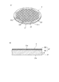
図1の(a)および(b)には、本発明によるリフトオフ方法によって移設基板に移し替えられる光デバイス層が形成された光デバイスウエーハの斜視図および要部拡大断面図が示されている。
図1の(a)および(b)に示す光デバイスウエーハ2は、直径が50mmで厚みが600μmの円板形状であるサファイア基板からなるエピタキシー基板21の表面21aにn型窒化ガリウム半導体層221およびp型窒化ガリウム半導体層222からなる光デバイス層22がエピタキシャル成長法によって形成されている。なお、エピタキシー基板21の表面にエピタキシャル成長法によってn型窒化ガリウム半導体層221およびp型窒化ガリウム半導体層222からなる光デバイス層22を積層する際に、エピタキシー基板21の表面21aと光デバイス層22を形成するn型窒化ガリウム半導体層221との間には窒化ガリウム(GaN)からなる厚みが例えば1μmのバッファー層23が形成される。このように構成された光デバイスウエーハ2は、図示の実施形態においては光デバイス層22の厚みが例えば10μmに形成されている。なお、光デバイス層22は、図1の(a)に示すように格子状に形成された複数のストリート223によって区画された複数の領域に光デバイス224が形成されている。
FIGS. 1A and 1B show a perspective view and an enlarged cross-sectional view of an essential part of an optical device wafer on which an optical device layer transferred to a transfer substrate by a lift-off method according to the present invention is formed.
An
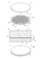
上述したように光デバイスウエーハ2におけるエピタキシー基板21を光デバイス層22から剥離して移設基板に移し替えるためには、光デバイス層22の表面22aに移設基板を接合して複合基板を形成する複合基板形成工程を実施する。即ち、図2の(a)、(b)および(c)に示すように、光デバイスウエーハ2を構成するエピタキシー基板21の表面21aに形成された光デバイス層22の表面22aに、厚みが1mmの銅基板からなる移設基板3を金錫(AuSn)からなる接合剤となる接合金属層4を介して接合する。なお、移設基板3としてはモリブデン(Mo)、銅(Cu)、シリコン(Si)等を用いることができ、また、接合金属層4を形成する接合金属としては金(Au),白金(Pt),クロム(Cr),インジウム(In),パラジウム(Pd)等を用いることができる。この複合基板形成工程は、エピタキシー基板21の表面21aに形成された光デバイス層22の表面22aまたは移設基板3の表面3aに上記接合金属を蒸着して厚みが3μm程度の接合金属層4を形成し、この接合金属層4と移設基板3の表面3aまたは光デバイス層22の表面22aとを対面させて圧着することにより、光デバイスウエーハ2を構成する光デバイス層22の表面22aに移設基板3の表面3aを接合金属層4を介して接合して複合基板200を形成する。なお、複合基板形成工程においてエピタキシー基板21の表面21aに形成された光デバイス層22の表面22aに移設基板3を接合して複合基板200を形成する際にエピタキシー基板21および移設基板3は250℃程度に加熱されるので、エピタキシー基板21と移設基板3との熱膨張係数の差により、複合基板200は常温において僅かに湾曲する。
As described above, in order to peel the
上述したように光デバイスウエーハ2を構成する光デバイス層22の表面22aに移設基板3の表面3aを接合金属層4を介して接合し複合基板200を形成したならば、複合基板200のエピタキシー基板21の裏面側からバッファー層23にエピタキシー基板21に対しては透過性を有しバッファー層23に対しては吸収性を有する波長のレーザー光線を照射し、バッファー層23を破壊するバッファー層破壊工程を実施する。バッファー層破壊工程は、図3に示すレーザー加工装置を用いて実施する。図3に示すレーザー加工装置5は、静止基台50と、該静止基台50に矢印Xで示す加工送り方向(X軸方向)に移動可能に配設され被加工物を保持するチャックテーブル機構6と、静止基台50に上記X軸方向と直交する矢印Yで示す割り出し送り方向(Y軸方向)に移動可能に配設されたレーザー光線照射ユニット支持機構7と、該レーザー光線照射ユニット支持機構7に矢印Zで示す集光点位置調整方向(Z軸方向)に移動可能に配設されたレーザー光線照射手段8とを具備している。
If the
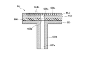
上記チャックテーブル機構6は、静止基台50上にX軸方向に沿って平行に配設された案内レール61、61と、該案内レール61、61上にX軸方向に移動可能に配設された第1の滑動ブロック62と、該第1の滑動ブロック62の上面に配設された案内レール621、621上にY軸方向に移動可能に配設された第2の滑動ブロック63と、該第2の滑動ブロック63上に円筒部材64によって支持されたカバーテーブル65と、被加工物保持手段としてのチャックテーブル66を具備している。このチャックテーブル66は、図4に示すようにチャックテーブル本体661と、該チャックテーブル本体661の保持領域660に配設された通気性を有する吸引保持部材として機能するポーラスセラミックスヒーター662とからなっている。チャックテーブル本体661は、円盤状の保持部661aと、該661aの下面に突出して設けられた回転軸部661bとからなっており、ステンレス鋼等の金属材やセラミックス等によって一体的に形成されている。保持部661aの上面には保持領域660に円形の嵌合凹部661cが設けられている。この嵌合凹部661cには、底面の外周部にポーラスセラミックスヒーター662が載置される環状の支持棚661dが設けられている。チャックテーブル本体661を形成する保持部611aおよび回転軸部611bには、嵌合凹部661cに開口する吸引通路611eが設けられている。
The
上記吸引保持部材として機能するポーラスセラミックスヒーター662は、チャックテーブル本体661の保持部661aの上面に形成された嵌合凹部661cに嵌合され環状の支持棚661d上に載置され、ポーラスセラミックスヒーター662の外周面と嵌合凹部661aの内周面が適宜の接着剤によって接合されている。このようにしてチャックテーブル本体661の保持部661aに設けられた嵌合凹部661cに嵌合されたポーラスセラミックスヒーター662は、その上面が保持部661aの上面と同一平面を形成するように構成されている。
The porous
以上のように構成されたチャックテーブル66は、チャックテーブル本体661に形成された吸引通路661eが図示しない吸引手段に接続される。従って、チャックテーブル本体661の保持領域660に配設されたポーラスセラミックスヒーター662上に被加工物を載置し、図示しない吸引手段を作動することにより、吸引通路661eを介してポーラスセラミックスヒーター662の上面に負圧が作用し、該ポーラスセラミックスヒーター662の上面に被加工物が吸引保持される。
In the chuck table 66 configured as described above, a
また、チャックテーブル66を構成するポーラスセラミックスヒーター662は、電源回路663に接続されている。従って、ポーラスセラミックスヒーター662は、電源回路663から電力が印加されることによって所定の温度に加熱される。なお、ポーラスセラミックスヒーター662の加熱温度は、100〜500℃が望ましい。
The porous
次に、チャックテーブル66の他の実施形態について、図5を参照して説明する。
図5に示すチャックテーブル66は、チャックテーブル本体661が上部部材664と下部部材665とからなっており、上部部材664と下部部材665との間にラバーヒーター666が配設されている。上部部材664には負圧室664aが設けられるとともに、該負圧室664aに連通し上面に開口する複数の吸引孔664bと下面に開口する連通孔664cが形成されている。また、下部部材665の下面に上記回転軸部661bが設けられている。なお、ラバーヒーター666の中心部には、上部部材664に形成された連通孔664cと下部部材665および回転軸部661bに形成された吸引通路661eと連通する連通路666aが設けられている。このように構成されたチャックテーブル66を構成するラバーヒーター666は、上記図4に示す実施形態と同様に電源回路に接続され、100〜500℃に加熱されるようになっている。
Next, another embodiment of the chuck table 66 will be described with reference to FIG.
In the chuck table 66 shown in FIG. 5, the chuck table
図3を参照して説明を続けると、上述したように構成されたチャックテーブル66は、円筒部材64内に配設された図示しないパルスモータによって回転せしめられる。また、図示のチャックテーブル機構6は、上記第1の滑動ブロック62を案内レール61、61に沿ってX軸方向に移動せしめる加工送り手段67と、第2の滑動ブロック63を案内レール621、621に沿ってY軸方向に移動せしめる第1の割り出し送り手段68を具備している。なお、加工送り手段67および第1の割り出し送り手段68は、周知のボールスクリュー機構によって構成されている。
Continuing the description with reference to FIG. 3, the chuck table 66 configured as described above is rotated by a pulse motor (not shown) disposed in the
上記レーザー光線照射ユニット支持機構7は、静止基台50上にY軸方向に沿って平行に配設された一対の案内レール71、71と、該案内レール71、71上にY軸方向に移動可能に配設された可動支持基台72を具備している。この可動支持基台72は、案内レール71、71上に移動可能に配設された移動支持部721と、該移動支持部721に取り付けられた装着部722とからなっており、ボールスクリュー機構によって構成された第2の割り出し送り手段73によって案内レール71、71に沿ってY軸方向に移動せしめられる。
The laser beam irradiation unit support mechanism 7 is movable in the Y-axis direction on a pair of
図示のレーザー光線照射手段8は、ユニットホルダ81と、該ユニットホルダ81に取り付けられたケーシング82を具備している。ユニットホルダ81は、上記可動支持基台72の装着部722に設けられた案内レール723、723に沿ってZ軸方向に移動可能に支持される。このように案内レール723、723に沿って移動可能に支持されたユニットホルダ81は、ボールスクリュー機構によって構成された集光点位置調整手段83によってZ軸方向に移動せしめられる。
The illustrated laser beam application means 8 includes a
図示のレーザー光線照射手段8は、上記ユニットホルダ81に固定され実質上水平に延出する円筒形状のケーシング82を含んでいる。ケーシング82内には図示しないパルスレーザー光線発振器や繰り返し周波数設定手段を備えたパルスレーザー光線発振手段が配設されている。上記ケーシング82の先端部には、パルスレーザー光線発振手段から発振されたパルスレーザー光線を集光するための集光器84が装着されている。ケーシング82の前端部には、上記レーザー光線照射手段8によって上記チャックテーブル66に保持された被加工物を撮像する撮像手段85が配設されている。この撮像手段85は、顕微鏡やCCDカメラ等の光学手段からなっており、撮像した画像信号を図示しない制御手段に送る。
The illustrated laser beam application means 8 includes a
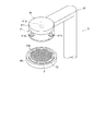
図示のレーザー加工装置5は、上記光デバイスウエーハ2を構成するエピタキシー基板21を光デバイス層22から剥離するための剥離機構9を具備している。剥離機構9は、上記チャックテーブル66に保持された光デバイスウエーハ2が剥離位置に位置付けられた状態でエピタキシー基板21を吸着する吸着手段91と、該吸着手段91を上下方向に移動可能に支持する支持手段92とからなっており、チャックテーブル機構6の一方の側に配設されている。吸着手段91は、保持部材911と、該保持部材911の下側に装着された複数(図示の実施形態においては3個)の吸引パッド912a,912b,912cとからなっており、吸引パッド912a,912b,912cが図示しない吸引手段に接続されている。
The illustrated
上記レーザー加工装置5を用いて複合基板200のエピタキシー基板21の裏面側からバッファー層23にエピタキシー基板21に対しては透過性を有しバッファー層23に対しては吸収性を有する波長のレーザー光線を照射し、バッファー層23を破壊するバッファー層破壊工程を実施するには、図4に示すチャックテーブル66を構成する吸引保持部材として機能するポーラスセラミックスヒーター662の上面、または図5に示すチャックテーブル66を構成するチャックテーブル本体661の上部部材664の上面に上記複合基板200の移設基板3側を載置する。そして、チャックテーブル66を構成するポーラスセラミックスヒーター662またはラバーヒーター666に電力を印加して100〜500℃に加熱する。この結果、チャックテーブル66上に吸引保持された複合基板200が100〜500℃に加熱される(複合基板加熱工程)。従って、常温において僅かに湾曲していた複合基板200を構成するエピタキシー基板21と移設基板3とに生じるスプリングバックが緩和される。
Using the
上述した複合基板加熱工程を実施したならば、図示しない吸引手段を作動することによってチャックテーブル66上に複合基板200を吸引保持する(ウエーハ保持工程)。従って、チャックテーブル66上に吸引保持された複合基板200は、光デバイスウエーハ2を構成するエピタキシー基板21の裏面21bが上側となる。このようにチャックテーブル66上に複合基板200を吸引保持したならば、加工送り手段67を作動してチャックテーブル66をレーザー光線照射手段8の集光器84が位置するレーザー光線照射領域に移動する。そして、図6の(a)で示すようにチャックテーブル66に保持された複合基板200の光デバイスウエーハ2を構成するエピタキシー基板21の一端(図6の(a)において左端)をレーザー光線照射手段8の集光器84の直下に位置付ける。次にレーザー光線照射手段8を作動して集光器84からバッファー層23にサファイアに対しては透過性を有しバッファー層23に対しては吸収性を有する波長のパルスレーザー光線を照射しつつチャックテーブル66を図6の(a)において矢印X1で示す方向に所定の加工送り速度で移動せしめる。そして、図6の(c)で示すようにレーザー光線照射手段8の集光器84の照射位置にエピタキシー基板21の他端(図6の(c)において右端)が達したら、パルスレーザー光線の照射を停止するとともにチャックテーブル66の移動を停止する。このバッファー層破壊工程をバッファー層23の全面に対応する領域に実施する。
なお、上記バッファー層破壊工程は、集光器84をエピタキシー基板21の最外周に位置付け、チャックテーブル66を回転しつつ集光器84を中心に向けて移動することによりバッファー層23の全面にパルスレーザー光線を照射してもよい。
When the above-described composite substrate heating step is performed, the
In the buffer layer destruction step, the
上記バッファー層破壊工程の加工条件は、次のように設定されている。
光源 :YAGレーザー
波長 :257nm
繰り返し周波数 :50kHz
平均出力 :0.12W
パルス幅 :100ns
スポット径 :φ70μm
デフォーカス :1.0mm(エピタキシー基板21の裏面21bにレー
ザー光線の集光点を位置付けた状態で集光器84を1mm
エピタキシー基板21に近づける。)
加工送り速度 :600mm/秒
The processing conditions for the buffer layer destruction step are set as follows.
Light source: YAG laser Wavelength: 257 nm
Repetition frequency: 50 kHz
Average output: 0.12W
Pulse width: 100 ns
Spot diameter: φ70μm
Defocused: 1.0 mm (on the
1 mm of
It approaches the epitaxy substrate 21. )
Processing feed rate: 600 mm / sec
上記加工条件によってバッファー層破壊工程を実施することにより、バッファー層23が破壊される。上述したバッファー層破壊工程においては、レーザー光線照射手段8を作動して集光器84からバッファー層23にサファイアに対しては透過性を有しバッファー層23に対しては吸収性を有する波長のパルスレーザー光線を照射する前に、チャックテーブル66上に吸引保持された複合基板200を加熱して、常温において僅かに湾曲していた複合基板200を構成するエピタキシー基板21と移設基板3とに生じるスプリングバックを緩和する複合基板加熱工程を実施するので、エピタキシー基板21および移設基板3のスプリングバックが生じることがないため、バッファー層23を確実に破壊することができる。
By performing the buffer layer destruction step under the above processing conditions, the
上述したバッファー層破壊工程を実施したならば、複合基板200のエピタキシー基板21を剥離し、光デバイス層22を移設基板3に移設する光デバイス層移設工程を実施する。即ち、チャックテーブル66を剥離機構9が配設された剥離位置に移動し、図7の(a)に示すようにチャックテーブル66に保持されている複合基板200を吸着手段91の直下に位置付ける。そして、図7の(b)に示すように吸着手段91を下降してエピタキシー基板21の裏面21bに吸引パッド912a、912b、912cを接触させ、図示しない吸引手段を作動することにより吸引パッド912a、912b、912cによってエピタキシー基板21の裏面21bを吸着する(エピタキシー基板吸着工程)。
When the buffer layer destruction step described above is performed, the optical device layer transfer step of peeling the
上述したエピタキシー基板吸着工程を実施したならば、エピタキシー基板21を吸着した吸引パッド912a,912b,912cをエピタキシー基板21から離反する方向に移動してエピタキシー基板21を剥離し、光デバイス層22を移設基板3に移設する剥離工程を実施する。即ち、上記図7の(b)に示すようにエピタキシー基板吸着工程を実施した状態から、図8に示すように吸着手段91を上方に移動することにより、エピタキシー基板21は光デバイス層22から剥離される。この結果、光デバイス層22が移設基板3に移し替えられたことになる。上記エピタキシー基板吸着工程および剥離工程とからなる光デバイス層移設工程が実施される複合基板200は上記バッファー層破壊工程においてバッファー層23が確実に破壊されているので、バッファー層23が破壊されていない領域で剥離することはない。従って、バッファー層23が破壊されていない領域で剥離が生じて光デバイス層22が破壊され、光デバイスの品質の低下を招くという問題が解消する。
If the above-described epitaxy substrate adsorption process is performed, the
2:光デバイスウエーハ
21:エピタキシー基板
22:光デバイス層
23:バッファー層
3:移設基板
4:接合金属層
200:複合基板
5:レーザー加工装置
6:チャックテーブル機構
66:チャックテーブル
662:ポーラスセラミックスヒーター
663:電源回路
666:ラバーヒーター
67:加工送り手段
7:レーザー光線照射ユニット支持機構
72:可動支持基台
8:レーザー光線照射手段
83:集光点位置調整手段
84:集光器
85:撮像手段
9:剥離機構
91:吸着手段
912a,912b,912c:吸引パッド
2: Optical device wafer 21: Epitaxy substrate 22: Optical device layer 23: Buffer layer 3: Transfer substrate 4: Bonded metal layer 200: Composite substrate 5: Laser processing device 6: Chuck table mechanism 66: Chuck table 662: Porous ceramic heater 663: Power supply circuit 666: Rubber heater 67: Processing feed means 7: Laser beam irradiation unit support mechanism 72: Movable support base 8: Laser beam irradiation means 83: Condensing point position adjusting means 84: Condenser 85: Imaging means 9: Peeling mechanism 91: suction means 912a, 912b, 912c: suction pad
Claims (2)
光デバイスウエーハの光デバイス層の表面に接合剤を介して移設基板を接合して複合基板を形成する複合基板形成工程と、
複合基板のエピタキシー基板の裏面側からバッファー層にエピタキシー基板に対しては透過性を有しバッファー層に対しては吸収性を有する波長のレーザー光線を照射し、バッファー層を破壊するバッファー層破壊工程と、
該バッファー層破壊工程が実施された複合基板のエピタキシー基板を剥離し、光デバイス層を移設基板に移設する光デバイス層移設工程と、を含み、
該バッファー層破壊工程は、複合基板を加熱してエピタキシー基板と移設基板とに生ずるスプリングバックを緩和させてレーザー光線をバッファー層に照射する、
ことを特徴とするリフトオフ方法。 A lift-off method for transferring an optical device layer of an optical device wafer in which an optical device layer is laminated on a surface of an epitaxy substrate via a buffer layer to a transfer substrate,
A composite substrate forming step of forming a composite substrate by bonding the transfer substrate to the surface of the optical device layer of the optical device wafer via a bonding agent;
A buffer layer destruction step of damaging the buffer layer by irradiating the buffer layer from the back side of the epitaxy substrate of the composite substrate with a laser beam having a wavelength that is transmissive to the epitaxy substrate and absorbing the buffer layer; ,
An optical device layer transfer step of peeling the epitaxy substrate of the composite substrate that has been subjected to the buffer layer destruction step, and transferring the optical device layer to the transfer substrate,
In the buffer layer destruction step, the composite substrate is heated to irradiate the buffer layer with a laser beam by relaxing the spring back generated between the epitaxy substrate and the transfer substrate.
A lift-off method characterized by that.
Priority Applications (5)
| Application Number | Priority Date | Filing Date | Title |
|---|---|---|---|
| JP2014016939A JP2015144192A (en) | 2014-01-31 | 2014-01-31 | lift-off method |
| TW103142144A TWI634671B (en) | 2014-01-31 | 2014-12-04 | Lift off method |
| CN201410827816.1A CN104821347A (en) | 2014-01-31 | 2014-12-25 | Lift-off method |
| US14/606,488 US9530929B2 (en) | 2014-01-31 | 2015-01-27 | Lift-off method |
| KR1020150013627A KR20150091246A (en) | 2014-01-31 | 2015-01-28 | Lift-off method |
Applications Claiming Priority (1)
| Application Number | Priority Date | Filing Date | Title |
|---|---|---|---|
| JP2014016939A JP2015144192A (en) | 2014-01-31 | 2014-01-31 | lift-off method |
Publications (1)
| Publication Number | Publication Date |
|---|---|
| JP2015144192A true JP2015144192A (en) | 2015-08-06 |
Family
ID=53731588
Family Applications (1)
| Application Number | Title | Priority Date | Filing Date |
|---|---|---|---|
| JP2014016939A Pending JP2015144192A (en) | 2014-01-31 | 2014-01-31 | lift-off method |
Country Status (5)
| Country | Link |
|---|---|
| US (1) | US9530929B2 (en) |
| JP (1) | JP2015144192A (en) |
| KR (1) | KR20150091246A (en) |
| CN (1) | CN104821347A (en) |
| TW (1) | TWI634671B (en) |
Cited By (4)
| Publication number | Priority date | Publication date | Assignee | Title |
|---|---|---|---|---|
| JP2017097059A (en) * | 2015-11-19 | 2017-06-01 | 日本電気硝子株式会社 | Patterning substrate manufacturing method and laminate |
| JP2019075480A (en) * | 2017-10-17 | 2019-05-16 | 株式会社ディスコ | Lift-off method |
| JPWO2021131710A1 (en) * | 2019-12-26 | 2021-07-01 | ||
| JPWO2021131711A1 (en) * | 2019-12-26 | 2021-07-01 |
Families Citing this family (5)
| Publication number | Priority date | Publication date | Assignee | Title |
|---|---|---|---|---|
| JP2017103405A (en) * | 2015-12-04 | 2017-06-08 | 株式会社ディスコ | Wafer processing method |
| CN105436710B (en) * | 2015-12-30 | 2019-03-05 | 大族激光科技产业集团股份有限公司 | A kind of laser-stripping method of Silicon Wafer |
| JP6985031B2 (en) * | 2017-05-19 | 2021-12-22 | 株式会社ディスコ | Manufacturing method of LED display panel |
| CN110021686A (en) * | 2018-09-01 | 2019-07-16 | 东莞市中晶半导体科技有限公司 | A kind of preparation method and extension Stacked wafer, chip of mini LED chip |
| JP7195700B2 (en) * | 2018-11-12 | 2022-12-26 | 株式会社ディスコ | Lift off method |
Citations (7)
| Publication number | Priority date | Publication date | Assignee | Title |
|---|---|---|---|---|
| JP2002144056A (en) * | 2000-11-06 | 2002-05-21 | Ibiden Co Ltd | Laser beam trimming stage |
| JP2003218470A (en) * | 2001-11-13 | 2003-07-31 | Matsushita Electric Ind Co Ltd | Semiconductor device and method of manufacturing the same |
| JP2010287681A (en) * | 2009-06-10 | 2010-12-24 | Toyoda Gosei Co Ltd | Method of manufacturing group iii nitride semiconductor light emitting element |
| JP2011049518A (en) * | 2009-08-26 | 2011-03-10 | Seoul Opto Devices Co Ltd | Method of manufacturing light emitting diode employing laser lift-off technology, and laser lift-off device having heater |
| JP2011054715A (en) * | 2009-09-01 | 2011-03-17 | Disco Abrasive Syst Ltd | Laser beam machining apparatus |
| US20110229999A1 (en) * | 2010-03-18 | 2011-09-22 | Kyung Wook Park | Fabrication method of light emitting device |
| JP2013179237A (en) * | 2012-02-29 | 2013-09-09 | Disco Abrasive Syst Ltd | Lift-off device |
Family Cites Families (14)
| Publication number | Priority date | Publication date | Assignee | Title |
|---|---|---|---|---|
| JPH10305420A (en) | 1997-03-04 | 1998-11-17 | Ngk Insulators Ltd | Method for fabricating matrix made up of oxide single crystal and method for manufacturing functional device |
| JP2003077940A (en) * | 2001-09-06 | 2003-03-14 | Sony Corp | Method of transferring device, method of arranging device using same, and method of manufacturing image display device unit |
| JP2004072052A (en) | 2002-08-09 | 2004-03-04 | Matsushita Electric Ind Co Ltd | Semiconductor device and manufacturing method thereof |
| US20090053845A1 (en) | 2005-11-14 | 2009-02-26 | Palo Alto Research Center Incorporated | Method For Controlling The Structure And Surface Qualities Of A Thin Film And Product Produced Thereby |
| JP5054933B2 (en) | 2006-05-23 | 2012-10-24 | ルネサスエレクトロニクス株式会社 | Manufacturing method of semiconductor device |
| US20090253273A1 (en) * | 2006-06-21 | 2009-10-08 | Hightec Systems Corporation | Method of heat-treating semiconductor |
| JP2011040564A (en) | 2009-08-11 | 2011-02-24 | Toshiba Corp | Method and apparatus for manufacturing semiconductor element |
| JP5345507B2 (en) | 2009-11-10 | 2013-11-20 | 株式会社ソフ.エンジニアリング | Lift-off device and lift-off processing method |
| US9123671B2 (en) | 2010-12-30 | 2015-09-01 | Taiwan Semiconductor Manufacturing Company, Ltd. | Silicon wafer strength enhancement |
| JP2011093803A (en) | 2011-02-02 | 2011-05-12 | Jx Nippon Mining & Metals Corp | Method for manufacturing gallium nitride-based compound semiconductor single crystal |
| JP5766530B2 (en) * | 2011-07-13 | 2015-08-19 | 株式会社ディスコ | Processing method of optical device wafer |
| JP6098028B2 (en) | 2011-09-14 | 2017-03-22 | 株式会社リコー | Gallium nitride crystal, group 13 nitride crystal, group 13 nitride crystal substrate, and manufacturing method |
| JP5860272B2 (en) * | 2011-11-24 | 2016-02-16 | 株式会社ディスコ | Processing method of optical device wafer |
| JP5996250B2 (en) * | 2012-04-24 | 2016-09-21 | 株式会社ディスコ | Lift-off method |
-
2014
- 2014-01-31 JP JP2014016939A patent/JP2015144192A/en active Pending
- 2014-12-04 TW TW103142144A patent/TWI634671B/en active
- 2014-12-25 CN CN201410827816.1A patent/CN104821347A/en active Pending
-
2015
- 2015-01-27 US US14/606,488 patent/US9530929B2/en active Active
- 2015-01-28 KR KR1020150013627A patent/KR20150091246A/en not_active Application Discontinuation
Patent Citations (7)
| Publication number | Priority date | Publication date | Assignee | Title |
|---|---|---|---|---|
| JP2002144056A (en) * | 2000-11-06 | 2002-05-21 | Ibiden Co Ltd | Laser beam trimming stage |
| JP2003218470A (en) * | 2001-11-13 | 2003-07-31 | Matsushita Electric Ind Co Ltd | Semiconductor device and method of manufacturing the same |
| JP2010287681A (en) * | 2009-06-10 | 2010-12-24 | Toyoda Gosei Co Ltd | Method of manufacturing group iii nitride semiconductor light emitting element |
| JP2011049518A (en) * | 2009-08-26 | 2011-03-10 | Seoul Opto Devices Co Ltd | Method of manufacturing light emitting diode employing laser lift-off technology, and laser lift-off device having heater |
| JP2011054715A (en) * | 2009-09-01 | 2011-03-17 | Disco Abrasive Syst Ltd | Laser beam machining apparatus |
| US20110229999A1 (en) * | 2010-03-18 | 2011-09-22 | Kyung Wook Park | Fabrication method of light emitting device |
| JP2013179237A (en) * | 2012-02-29 | 2013-09-09 | Disco Abrasive Syst Ltd | Lift-off device |
Cited By (9)
| Publication number | Priority date | Publication date | Assignee | Title |
|---|---|---|---|---|
| JP2017097059A (en) * | 2015-11-19 | 2017-06-01 | 日本電気硝子株式会社 | Patterning substrate manufacturing method and laminate |
| JP2019075480A (en) * | 2017-10-17 | 2019-05-16 | 株式会社ディスコ | Lift-off method |
| JP7007053B2 (en) | 2017-10-17 | 2022-01-24 | 株式会社ディスコ | Lift-off method |
| JPWO2021131710A1 (en) * | 2019-12-26 | 2021-07-01 | ||
| JPWO2021131711A1 (en) * | 2019-12-26 | 2021-07-01 | ||
| WO2021131710A1 (en) * | 2019-12-26 | 2021-07-01 | 東京エレクトロン株式会社 | Substrate processing apparatus, and substrate processing method |
| WO2021131711A1 (en) * | 2019-12-26 | 2021-07-01 | 東京エレクトロン株式会社 | Substrate processing method and substrate processing apparatus |
| JP7304433B2 (en) | 2019-12-26 | 2023-07-06 | 東京エレクトロン株式会社 | Substrate processing method and substrate processing apparatus |
| JP7308292B2 (en) | 2019-12-26 | 2023-07-13 | 東京エレクトロン株式会社 | SUBSTRATE PROCESSING APPARATUS AND SUBSTRATE PROCESSING METHOD |
Also Published As
| Publication number | Publication date |
|---|---|
| US20150221818A1 (en) | 2015-08-06 |
| US9530929B2 (en) | 2016-12-27 |
| TWI634671B (en) | 2018-09-01 |
| KR20150091246A (en) | 2015-08-10 |
| CN104821347A (en) | 2015-08-05 |
| TW201530803A (en) | 2015-08-01 |
Similar Documents
| Publication | Publication Date | Title |
|---|---|---|
| JP2015144192A (en) | lift-off method | |
| JP5996254B2 (en) | Lift-off method | |
| KR102217032B1 (en) | Lift-off method | |
| TWI538041B (en) | Processing method of optical element wafers | |
| JP5996250B2 (en) | Lift-off method | |
| TWI574314B (en) | Wafer processing method | |
| KR20140126247A (en) | Wafer machining method | |
| JP2015216301A (en) | Processing method of wafer | |
| JP6523882B2 (en) | Wafer processing method | |
| JP2011233641A (en) | Laser processing method for plate-like object | |
| JP6294090B2 (en) | Lift-off method | |
| KR20130054912A (en) | Optical device layer transferring apparatus and laser machining apparatus | |
| JP2015204367A (en) | Processing method of optical device wafer | |
| JP2006186263A (en) | Workpiece holding device | |
| CN111834275A (en) | Processing method and hot-press bonding method for processed object | |
| JP2024058321A (en) | Wafer processing method | |
| JP5879131B2 (en) | Substrate peeling method | |
| JP5988644B2 (en) | Processing method of optical device wafer |
Legal Events
| Date | Code | Title | Description |
|---|---|---|---|
| A621 | Written request for application examination |
Free format text: JAPANESE INTERMEDIATE CODE: A621 Effective date: 20161117 |
|
| A977 | Report on retrieval |
Free format text: JAPANESE INTERMEDIATE CODE: A971007 Effective date: 20170816 |
|
| A131 | Notification of reasons for refusal |
Free format text: JAPANESE INTERMEDIATE CODE: A131 Effective date: 20170822 |
|
| A521 | Request for written amendment filed |
Free format text: JAPANESE INTERMEDIATE CODE: A523 Effective date: 20171018 |
|
| A131 | Notification of reasons for refusal |
Free format text: JAPANESE INTERMEDIATE CODE: A131 Effective date: 20180206 |
|
| A02 | Decision of refusal |
Free format text: JAPANESE INTERMEDIATE CODE: A02 Effective date: 20180731 |