WO2021131710A1 - Substrate processing apparatus, and substrate processing method - Google Patents
Substrate processing apparatus, and substrate processing method Download PDFInfo
- Publication number
- WO2021131710A1 WO2021131710A1 PCT/JP2020/045883 JP2020045883W WO2021131710A1 WO 2021131710 A1 WO2021131710 A1 WO 2021131710A1 JP 2020045883 W JP2020045883 W JP 2020045883W WO 2021131710 A1 WO2021131710 A1 WO 2021131710A1
- Authority
- WO
- WIPO (PCT)
- Prior art keywords
- substrate
- laser
- wafer
- peeling
- laser beam
- Prior art date
Links
Images


Classifications
-
- B—PERFORMING OPERATIONS; TRANSPORTING
- B23—MACHINE TOOLS; METAL-WORKING NOT OTHERWISE PROVIDED FOR
- B23K—SOLDERING OR UNSOLDERING; WELDING; CLADDING OR PLATING BY SOLDERING OR WELDING; CUTTING BY APPLYING HEAT LOCALLY, e.g. FLAME CUTTING; WORKING BY LASER BEAM
- B23K26/00—Working by laser beam, e.g. welding, cutting or boring
- B23K26/50—Working by transmitting the laser beam through or within the workpiece
- B23K26/57—Working by transmitting the laser beam through or within the workpiece the laser beam entering a face of the workpiece from which it is transmitted through the workpiece material to work on a different workpiece face, e.g. for effecting removal, fusion splicing, modifying or reforming
-
- H—ELECTRICITY
- H01—ELECTRIC ELEMENTS
- H01L—SEMICONDUCTOR DEVICES NOT COVERED BY CLASS H10
- H01L21/00—Processes or apparatus adapted for the manufacture or treatment of semiconductor or solid state devices or of parts thereof
- H01L21/02—Manufacture or treatment of semiconductor devices or of parts thereof
-
- H—ELECTRICITY
- H01—ELECTRIC ELEMENTS
- H01L—SEMICONDUCTOR DEVICES NOT COVERED BY CLASS H10
- H01L21/00—Processes or apparatus adapted for the manufacture or treatment of semiconductor or solid state devices or of parts thereof
- H01L21/67—Apparatus specially adapted for handling semiconductor or electric solid state devices during manufacture or treatment thereof; Apparatus specially adapted for handling wafers during manufacture or treatment of semiconductor or electric solid state devices or components ; Apparatus not specifically provided for elsewhere
- H01L21/683—Apparatus specially adapted for handling semiconductor or electric solid state devices during manufacture or treatment thereof; Apparatus specially adapted for handling wafers during manufacture or treatment of semiconductor or electric solid state devices or components ; Apparatus not specifically provided for elsewhere for supporting or gripping
Definitions
- This disclosure relates to a substrate processing apparatus and a substrate processing method.
- Patent Document 1 discloses a method for manufacturing a semiconductor device.
- Such a method for manufacturing a semiconductor device includes a heating step of irradiating a CO 2 laser from the back surface of the semiconductor substrate to locally heat the peeled oxide film, and in the peeled oxide film and / or the interface between the peeled oxide film and the semiconductor substrate.
- the technique according to the present disclosure appropriately transfers a device layer formed on the surface of a second substrate to a first substrate in a polymerized substrate in which a first substrate and a second substrate are bonded.
- One aspect of the present disclosure is an apparatus for transferring a device layer formed on the surface of the second substrate to the first substrate in a polymerized substrate in which a first substrate and a second substrate are bonded.
- a laser irradiation unit that irradiates a laser beam from the back surface side of the second substrate, a peeling unit that peels the second substrate from the first substrate, and a control unit that controls the operation of the laser irradiation unit.
- control unit forms a peeling region of the first substrate and the second substrate irradiated with the laser beam and a non-peeling region not irradiated with the laser beam.
- the laser irradiation unit is controlled so as to do so.
- a device layer formed on the surface of the second substrate can be appropriately transferred to the first substrate.
- laser lift-off is performed in which a GaN (gallium nitride) -based compound crystal layer (material layer) is peeled off from a sapphire substrate using laser light.
- the sapphire substrate has transparency to short-wavelength laser light (for example, UV light)
- short-wavelength laser light having a high absorption rate for the absorption layer is used.
- laser light for example, UV light
- the device layer formed on the surface of one substrate is transferred to another substrate.
- Silicon substrates are generally transparent to laser light in the NIR (near infrared) region, but the absorption layer is also transparent to NIR laser light, so the device layer may be damaged. There is. Therefore, in order to perform laser lift-off in the semiconductor device manufacturing process, laser light in the FIR (far infrared) region is used.
- a laser beam having a wavelength of FIR can be used, for example by a CO 2 laser.
- the exfoliated oxide film is irradiated with a CO 2 laser to cause exfoliation at the interface between the exfoliated oxide film and the substrate.
- the exfoliated oxide film is locally irradiated with a CO 2 laser.
- the part where the peeling occurs is too small when only a part of the peeling oxide film is irradiated with the CO 2 laser in this way, and the peeling of the substrate from the peeling oxide film is appropriate. It turns out that it may not be done. Therefore, it is necessary to increase the range of irradiating the CO 2 laser to the oxidative peeling film so that the substrate can be peeled off.
- the chuck holding the substrate is rotated or moved to increase the range in which the CO 2 laser is irradiated.
- the technique according to the present disclosure appropriately transfers a device layer formed on the surface of a second substrate to a first substrate in a polymerized substrate in which a first substrate and a second substrate are bonded.
- a wafer processing system including a laser irradiation device as a substrate processing apparatus and a wafer processing method as a substrate processing method according to the present embodiment will be described with reference to the drawings.
- elements having substantially the same functional configuration are designated by the same reference numerals, so that duplicate description will be omitted.
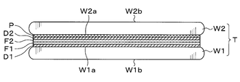
- the wafer processing system 1 as a polymerization substrate in which the first wafer W1 as the first substrate and the second wafer W2 as the second substrate are bonded. Processing is performed on the polymerized wafer T of.
- the first wafer W1 the surface on the side bonded to the second wafer W2 is referred to as the front surface W1a, and the surface opposite to the front surface W1a is referred to as the back surface W1b.
- the front surface W2a the surface on the side joined to the first wafer W1
- the back surface W2b the surface opposite to the front surface W2a
- the first wafer W1 is a semiconductor wafer such as a silicon substrate.
- the device layer D1 and the surface film F1 are laminated on the surface W1a of the first wafer W1 in this order from the surface W1a side.
- the device layer D1 includes a plurality of devices.
- Examples of the surface film F1 include an oxide film (SiO 2 film, TEOS film), a SiC film, a SiCN film, and an adhesive.
- the device layer D1 and the surface film F1 may not be formed on the surface W1a.
- the second wafer W2 is also a semiconductor wafer such as a silicon substrate.
- the laser absorption layer P, the device layer D2, and the surface film F2 are laminated on the surface W2a of the second wafer W2 in this order from the surface W2a side.
- the laser absorption layer P absorbs the laser light emitted from the laser head 110 as described later.
- An oxide film SiO 2 film
- the laser absorption layer P is not particularly limited as long as it absorbs laser light.
- the device layer D2 and the surface film F2 are the same as the device layer D1 and the surface film F1 of the first wafer W1, respectively.
- the surface film F1 of the first wafer W1 and the surface film F2 of the second wafer W2 are joined.
- the position of the laser absorption layer P is not limited to the above embodiment, and may be formed between the device layer D2 and the surface film F2, for example. Further, the device layer D2 and the surface film F2 may not be formed on the surface W2a. In this case, the laser absorption layer P is formed on the first wafer W1 side, and the device layer D1 on the first wafer W1 side is transferred to the second wafer W2 side.
- the wafer processing system 1 has a configuration in which the loading / unloading block 10, the transport block 20, and the processing block 30 are integrally connected.
- the carry-in / out block 10 and the processing block 30 are provided around the transport block 20.
- the carry-in / out block 10 is arranged on the Y-axis negative direction side of the transport block 20.
- the laser irradiation device 31 described later of the processing block 30 is arranged on the negative side of the X-axis of the transport block 20, and the cleaning device 32 described later is arranged on the positive side of the X-axis of the transport block 20.
- cassettes Ct, Cw1 and Cw2 capable of accommodating a plurality of polymerization wafers T, a plurality of first wafers W1 and a plurality of second wafers W2 are carried in / out from the outside.
- the carry-in / out block 10 is provided with a cassette mounting stand 11.
- a plurality of, for example, three cassettes Ct, Cw1 and Cw2 can be freely mounted in a row on the cassette mounting table 11 in the X-axis direction.
- the number of cassettes Ct, Cw1 and Cw2 mounted on the cassette mounting table 11 is not limited to this embodiment and can be arbitrarily determined.
- the transfer block 20 is provided with a wafer transfer device 22 configured to be movable on a transfer path 21 extending in the X-axis direction.
- the wafer transfer device 22 has, for example, two transfer arms 23, 23 that hold and transfer the polymerized wafer T, the first wafer W1, and the second wafer W2.
- Each transport arm 23 is configured to be movable in the horizontal direction, the vertical direction, the horizontal axis, and the vertical axis.
- the configuration of the transport arm 23 is not limited to this embodiment, and any configuration can be adopted.
- the wafer transfer device 22 and the wafer transfer device 22 have the polymer wafer T, the first wafer, with respect to the cassettes Ct, Cw1, Cw2 of the cassette mounting table 11, the laser irradiation device 31 and the cleaning device 32 described later. It is configured to be able to convey W1 and the second wafer W2.
- the processing block 30 has a laser irradiation device 31 and a cleaning device 32.
- the laser irradiation device 31 irradiates the laser absorption layer P of the second wafer W2 with laser light.
- the configuration of the laser irradiation device 31 will be described later.
- the cleaning device 32 cleans the surface of the laser absorption layer P formed on the surface W1a of the first wafer W1 separated by the laser irradiation device 31. For example, a brush is brought into contact with the surface of the laser absorption layer P, and the surface is scrubbed. A pressurized cleaning liquid may be used for cleaning the surface. Further, the cleaning device 32 may have a configuration for cleaning the back surface W1b together with the front surface W1a side of the first wafer W1.
- the above wafer processing system 1 is provided with a control device 40 as a control unit.
- the control device 40 is, for example, a computer and has a program storage unit (not shown).
- the program storage unit stores a program that controls the processing of the polymerized wafer T in the wafer processing system 1. Further, the program storage unit also stores a program for controlling the operation of the drive system of the above-mentioned various processing devices and transfer devices to realize the wafer processing described later in the wafer processing system 1.
- the program may be recorded on a computer-readable storage medium H and may be installed on the control device 40 from the storage medium H.
- the laser irradiation device 31 has a chuck 100 as a holding portion for holding the polymerized wafer T on the upper surface.
- the chuck 100 attracts and holds the entire surface of the back surface W1b of the first wafer W1.
- the chuck 100 may suck and hold a part of the back surface W1b.
- the chuck 100 is provided with an elevating pin (not shown) for supporting and elevating the polymerization wafer T from below.
- the elevating pin is configured to be elevating and lowering by inserting a through hole (not shown) formed through the chuck 100.
- a holding portion (not shown) for holding the second wafer W2 may be provided outside the chuck 100.
- the presence of the non-peeling region B prevents the second wafer W2 from slipping or slipping from the laser absorption layer P, but the slipping or slipping is more reliably prevented by the holding portion. can do.
- the chuck 100 is supported by the slider table 102 via the air bearing 101.
- a rotation mechanism 103 is provided on the lower surface side of the slider table 102.
- the rotation mechanism 103 has, for example, a built-in motor as a drive source.
- the chuck 100 is rotatably configured around the ⁇ axis (vertical axis) by the rotation mechanism 103 via the air bearing 101.
- the slider table 102 is configured to be movable along a rail 105 provided on the base 106 and extending in the Y-axis direction by a moving mechanism 104 provided on the lower surface side thereof.
- the drive source of the moving mechanism 104 is not particularly limited, but for example, a linear motor is used.
- a laser head 110 as a laser irradiation unit is provided above the chuck 100.
- the laser head 110 has a lens 111.
- the lens 111 is a tubular member provided on the lower surface of the laser head 110, and irradiates the polymerized wafer T held by the chuck 100 with laser light.
- the laser beam is a CO 2 laser beam
- the laser beam emitted from the laser head 110 passes through the second wafer W2 and irradiates the laser absorption layer P.
- the wavelength of the CO 2 laser beam is, for example, 8.9 ⁇ m to 11 ⁇ m.
- the laser head 110 is configured to be able to move up and down by an elevating mechanism (not shown).
- the light source of the laser beam is provided at a remote position outside the laser head 110.
- a transport pad 120 as a peeling portion is provided above the chuck 100.
- the transport pad 120 is configured to be able to move up and down by an elevating mechanism (not shown). Further, the transport pad 120 has a suction surface of the second wafer W2. Then, the transfer pad 120 transfers the second wafer W2 between the chuck 100 and the transfer arm 23. Specifically, after moving the chuck 100 to the lower side of the transfer pad 120 (the delivery position with the transfer arm 23), the transfer pad 120 sucks and holds the back surface W2b of the second wafer W2, and the first wafer W1 Peel off from. Subsequently, the peeled second wafer W2 is transferred from the transfer pad 120 to the transfer arm 23 and carried out from the laser irradiation device 31.
- the transfer pad 120 may be configured to invert the front and back surfaces of the wafer by an inversion mechanism (not shown).
- the transfer arm 23 accesses the transfer pad 120 from the positive direction side of the X axis.
- the laser irradiation device 31 shown in FIG. 4 may be rotated 90 degrees counterclockwise, and the transfer arm 23 may access the transfer pad 120 from the negative direction of the Y axis.
- the polymerized wafer T When the polymerized wafer T is carried into the laser irradiation device 31, the polymerized wafer T is delivered from the transport arm 23 to the elevating pin, and is placed on the chuck 100 by lowering the elevating pin. Further, when the peeled first wafer W1 is carried out from the laser irradiation device 31, the polymerized wafer T placed on the chuck 100 is raised by the elevating pin and delivered from the elevating pin to the transfer arm 23.
- the wafer processing performed by using the wafer processing system 1 configured as described above will be described.
- the first wafer W1 and the second wafer W2 are bonded to each other in an external bonding device (not shown) of the wafer processing system 1 to form a polymerized wafer T in advance.
- a cassette Ct containing a plurality of polymerized wafers T is placed on the cassette mounting table 11 of the loading / unloading block 10.
- the polymerized wafer T in the cassette Ct is taken out by the wafer transfer device 22 and transferred to the laser irradiation device 31.
- the laser irradiation device 31 the polymerized wafer T is transferred from the transfer arm 23 to the elevating pin and is attracted and held by the chuck 100.
- the moving mechanism 104 moves the chuck 100 to the processing position.
- This processing position is a position where the laser beam can be irradiated from the laser head 110 to the polymerized wafer T (laser absorption layer P).
- the laser head 110 irradiates the laser absorption layer P with the laser beam L (CO 2 laser beam) in a pulsed manner.
- the laser beam L passes through the second wafer W2 from the back surface W2b side of the second wafer W2 and is absorbed by the laser absorption layer P.
- the laser beam L causes peeling at the interface between the laser absorption layer P and the second wafer W2. Almost all the laser light L is absorbed by the laser absorption layer P and does not reach the device layer D2. Therefore, it is possible to prevent the device layer D2 from being damaged.
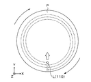
- the rotation mechanism 103 rotates the chuck 100 (polymerized wafer T), and the movement mechanism 104 moves the chuck 100 in the Y-axis direction. Then, the laser beam L is irradiated to the laser absorption layer P from the outer side to the inner side in the radial direction, and as a result, is spirally irradiated from the outer side to the inner side.
- the black arrow shown in FIG. 6 indicates the rotation direction of the chuck 100.
- the irradiation start position of the laser beam L is preferably between the outer peripheral edge Ea of the second wafer W2 and the junction end Eb of the first wafer W1 and the second wafer W2 in the polymerization wafer T.
- the eccentricity is absorbed and the laser beam L is applied to the laser absorption layer P. It can be irradiated appropriately.
- the laser beam L may be irradiated concentrically in an annular shape.
- the rotation of the chuck 100 and the Y direction of the chuck 100 are alternately performed, it is better to irradiate the laser beam L in a spiral shape as described above to shorten the irradiation time and improve the throughput. Can be done.
- the laser beam L may be irradiated from the inside to the outside in the radial direction.
- the stress due to the peeling may be directed outward in the radial direction, and the portion outside which the laser beam L is not irradiated may also be peeled off.
- the stress associated with the peeling can be released to the outside, so that the peeling can be controlled more easily. Further, by appropriately controlling the peeling, it is possible to suppress the roughness of the peeled surface.
- the chuck 100 when the laser absorption layer P is irradiated with the laser beam L, the chuck 100 is rotated, but the laser head 110 is moved and the laser head 110 is rotated relative to the chuck 100. May be good. Further, although the chuck 100 is moved in the Y-axis direction, the laser head 110 may be moved in the Y-axis direction.
- the chuck 100 rotates, so that the second wafer W2 is subjected to. Centrifugal force acts to cause the second wafer W2 to shift from the laser absorption layer P, and the laser beam L may be irradiated to a place other than the processing target position during the laser processing. In addition, the second wafer W2 may slide off the chuck 100.
- a peeling region A and a non-peeling region B are formed in the laser absorption layer P as shown in FIG.
- the peeling region A is a region to which the laser beam L is irradiated, and in this peeling region A, peeling occurs at the interface between the laser absorption layer P and the second wafer W2.
- the non-peeling region B is a region not irradiated with the laser beam L, and in this non-peeling region B, peeling does not occur at the interface between the laser absorption layer P and the second wafer W2, and the laser absorption layer P and the non-peeling region B The second wafer W2 is joined.
- the laser beam L can be irradiated to an appropriate position.
- the irradiation of the laser beam L from the laser head 110 may be stopped at the position where the non-peeling region B is to be formed.
- non-peeling regions B are formed at the central portion of the laser absorption layer P and four peripheral edges thereof, but the positions and numbers of the non-peeling regions B are arbitrary.
- the non-peelable region B may be formed to such an extent that the second wafer W2 does not shift or slide down.
- the range of the peeling region A is set to the non-peeling region B in order to prevent a large load from being applied. Make it larger than the range.
- the laser irradiation device 31 irradiates the laser beam L in a pulse shape so that the peeling region A and the non-peeling region B are formed on the laser absorbing layer P.
- the cause of the peeling is not the energy amount of the laser beam L but the peak power (maximum intensity of the laser beam).
- the laser beam L is continuously oscillated (when a continuous wave is used), it is difficult to increase the peak power, and peeling may not occur.
- the laser beam L when the laser beam L is oscillated in a pulse shape (when a pulse wave is used), the peak power can be increased to cause peeling at the interface between the laser absorption layer P and the second wafer W2. , The second wafer W2 can be appropriately peeled from the laser absorption layer P.
- the laser beam obtained by oscillating the CO 2 laser in a pulse shape is a so-called pulse laser, and its power repeats 0 (zero) and the maximum value.
- the chuck 100 is moved to the delivery position by the moving mechanism 104.
- an inertial force acts on the second wafer W2, and the second wafer W2 may be displaced from the laser absorption layer P.
- the back surface W2b of the second wafer W2 is subsequently sucked and held by the transport pad 120, an appropriate position cannot be sucked and held.
- the non-peelable region B is formed in the laser absorption layer P, it is possible to prevent the second wafer W2 from shifting.
- the transfer pad 120 sucks and holds the back surface W2b of the second wafer W2. Then, as shown in FIG. 9B, with the transport pad 120 adsorbing and holding the second wafer W2, the transport pad 120 is raised to peel the second wafer W2 from the laser absorption layer P. At this time, since the non-peeling region B is formed in the laser absorbing layer P, a load is applied to the extent that the second wafer W2 can be peeled from the laser absorbing layer P in this non-peeling region B. Then, the second wafer W2 can be peeled from the laser absorption layer P.
- the transfer pad 120 may be rotated around the vertical axis to peel off the second wafer W2.
- the peeled second wafer W2 is delivered from the transfer pad 120 to the transfer arm 23 of the wafer transfer device 22, and is transferred to the cassette Cw2 of the cassette mounting table 11.
- the second wafer W2 carried out from the laser irradiation device 31 may be conveyed to the cleaning device 32 before being conveyed to the cassette Cw2, and the surface W2a which is the peeling surface thereof may be cleaned.
- the front and back surfaces of the second wafer W2 may be inverted by the transfer pad 120 and transferred to the transfer arm 23.
- the first wafer W1 held by the chuck 100 is raised from the chuck 100 by the elevating pin, delivered to the transport arm 23, and transported to the cleaning device 32.
- the surface of the laser absorption layer P which is the peeling surface, is scrubbed.
- the back surface W1b of the first wafer W1 may be cleaned together with the front surface of the laser absorption layer P.
- a cleaning unit for cleaning the front surface of the laser absorption layer P and the back surface W1b of the first wafer W1 may be provided separately.
- the first wafer W1 that has been subjected to all the processing is transferred to the cassette Cw1 of the cassette mounting table 11 by the wafer transfer device 22. In this way, a series of wafer processing in the wafer processing system 1 is completed.
- the non-peeling region B when the laser beam L is spirally irradiated from the radial outside to the inside of the laser absorption layer P, the non-peeling region B is formed, so that even if the chuck 100 is rotated, the second It is possible to prevent the wafer W2 from slipping or slipping. Further, even when the chuck 100 moves after the irradiation with the laser beam L, the non-peeling region B can prevent the second wafer W2 from shifting. Therefore, the second wafer W2 can be appropriately peeled from the laser absorption layer P, and the device layer D2 can be transferred to the first wafer W1.
- the laser absorption layer P is irradiated with the laser beam L in a spiral or concentric pattern, but the irradiation pattern of the laser beam L is not limited to this.
- the configuration of the device corresponding to such various irradiation patterns is not limited to the laser irradiation device 31 of the above embodiment.
- the chuck 100 is rotatable around the ⁇ axis and movable in the uniaxial (Y axis) direction, but may be moved in two axes (X axis and Y axis).
- a galvano may be used for the laser head 110, and the laser light L emitted from the laser head 110 may be scanned against the laser absorption layer P.
- the laser beam L is scanned in a predetermined scanning range of the laser absorption layer P.
- the chuck 100 is moved in the X-axis direction while the irradiation of the laser beam L is stopped. In this way, the irradiation and scanning of the laser beam L and the movement of the chuck 100 are repeatedly performed to irradiate the laser beam L in a row in the X-axis direction.
- the chuck 100 is moved so as to be displaced in the Y-axis direction, and the irradiation and scanning of the laser beam L and the movement of the chuck 100 are repeatedly performed in the same manner as described above to irradiate the laser beam L in a row in the X-axis direction. To do. Then, the laser beam L is applied to the laser absorption layer P.
- the irradiation and scanning of the laser beam L and the movement of the chuck 100 were repeatedly performed, but the irradiation and scanning of the laser beam L and the movement of the chuck 100 were performed while moving the chuck 100 in a row in the X-axis direction. Scanning may be performed. Then, after irradiating the laser beam L in a row in the X-axis direction, the chuck 100 is moved so as to be displaced in the Y-axis direction, and the laser beam L is irradiated to the laser absorption layer P.
- the irradiation of the spiral (or concentric) laser beam L of the above embodiment may be combined with the irradiation and scanning of the laser beam L.
- the rotation speed of the chuck 100 increases as the laser beam L moves from the outer side to the inner side in the radial direction. Therefore, on the outer peripheral portion of the laser absorption layer P, the chuck 100 is moved from the outside in the radial direction to the inside while rotating the chuck 100, and the laser beam L is spirally irradiated. Then, when the rotation speed of the chuck 100 reaches the upper limit, the rotation of the chuck 100 is stopped at the central portion of the laser absorption layer P, and scanning is performed while irradiating the laser beam L.
- the laser beam L is prevented from overlapping, and the interval of irradiating the laser beam L, that is, the interval of the pulse is made constant. can do.
- the first wafer W1 and the second wafer W2 can be uniformly peeled off in the wafer surface.
- the wafer processing system 1 of the above embodiment has a cleaning device 32, but the wafer processing system 1 may further have an etching device (not shown).
- the etching apparatus etches the surface W1a of the first wafer W1 after peeling, specifically, the surface of the laser absorption layer P.
- a chemical solution etching solution
- the wafer processing system 1 may have either a cleaning device 32 or an etching device.
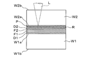
- a reflective film R may be provided between the laser absorption layer P and the device layer D2 as shown in FIG. That is, the reflective film R is formed on the surface of the laser absorbing layer P opposite to the incident surface of the laser beam L.
- a material having a high reflectance to the laser beam L and a high melting point for example, a metal film is used.
- the device layer D2 is a layer having a function and is different from the reflective film R.
- the laser beam L emitted from the laser head 110 passes through the second wafer W2 and is almost completely absorbed by the laser absorption layer P, but even if there is a laser beam L that cannot be completely absorbed. It is reflected by the reflective film R. As a result, the laser beam L does not reach the device layer D2, and it is possible to reliably suppress the device layer D2 from being damaged.
- the laser beam L reflected by the reflective film R is absorbed by the laser absorption layer P. Therefore, the peeling efficiency of the second wafer W2 can be improved.
- Laser irradiation device 40 Control device 100 Chuck 110 Laser head 120 Conveyor pad A Peeling area B Non-peeling area D1, D2 Device layer P Laser absorption layer T Polymerized wafer W1 First wafer W2 Second wafer
Landscapes
- Engineering & Computer Science (AREA)
- Physics & Mathematics (AREA)
- Optics & Photonics (AREA)
- Condensed Matter Physics & Semiconductors (AREA)
- Power Engineering (AREA)
- Microelectronics & Electronic Packaging (AREA)
- Computer Hardware Design (AREA)
- Manufacturing & Machinery (AREA)
- General Physics & Mathematics (AREA)
- Chemical Kinetics & Catalysis (AREA)
- Mechanical Engineering (AREA)
- Plasma & Fusion (AREA)
- Oil, Petroleum & Natural Gas (AREA)
- General Chemical & Material Sciences (AREA)
- Chemical & Material Sciences (AREA)
- Container, Conveyance, Adherence, Positioning, Of Wafer (AREA)
- Laser Beam Processing (AREA)
Abstract
This apparatus for transferring a device layer formed on the surface of a second substrate to a first substrate, in a superimposed substrate in which the first substrate and the second substrate are bonded together, includes a holding unit for holding the reverse surface of the first substrate, a laser radiating unit for radiating laser light from the reverse surface side of the second substrate onto a laser absorbing layer formed between the second substrate and the device layer, with the first substrate being held by the holding portion, a detaching unit for detaching the second substrate from the first substrate, and a control unit for controlling the operation of the laser radiating unit, wherein the control unit controls the laser radiating unit in such a way as to form, in the laser absorbing layer, a detachment region of the first substrate and the second substrate upon which the laser light is radiated, and a non-detachment region upon which the laser light is not radiated.
Description
本開示は、基板処理装置及び基板処理方法に関する。
This disclosure relates to a substrate processing apparatus and a substrate processing method.
特許文献1には、半導体装置の製造方法が開示されている。かかる半導体装置の製造方法は、半導体基板の裏面よりCO2レーザを照射して剥離酸化膜を局所的に加熱する加熱工程と、剥離酸化膜中、及び/又は剥離酸化膜と半導体基板との界面において剥離を生じさせて、半導体素子を転写先基板に転写させる転写工程と、を含む。
Patent Document 1 discloses a method for manufacturing a semiconductor device. Such a method for manufacturing a semiconductor device includes a heating step of irradiating a CO 2 laser from the back surface of the semiconductor substrate to locally heat the peeled oxide film, and in the peeled oxide film and / or the interface between the peeled oxide film and the semiconductor substrate. Includes a transfer step of causing peeling in the above to transfer the semiconductor element to the transfer destination substrate.
本開示にかかる技術は、第1の基板と第2の基板が接合された重合基板において、第2の基板の表面に形成されたデバイス層を第1の基板に適切に転写する。
The technique according to the present disclosure appropriately transfers a device layer formed on the surface of a second substrate to a first substrate in a polymerized substrate in which a first substrate and a second substrate are bonded.
本開示の一態様は、第1の基板と第2の基板が接合された重合基板において、前記第2の基板の表面に形成されたデバイス層を前記第1の基板に転写する装置であって、前記第1の基板の裏面を保持する保持部と、前記保持部が前記第1の基板を保持した状態で、前記第2の基板と前記デバイス層の間に形成されたレーザ吸収層に対して、当該第2の基板の裏面側からレーザ光を照射するレーザ照射部と、前記第1の基板から前記第2の基板を剥離する剥離部と、前記レーザ照射部の動作を制御する制御部と、を有し、前記制御部は、前記レーザ吸収層において、前記レーザ光が照射される第1の基板と第2の基板の剥離領域と、前記レーザ光が照射されない非剥離領域とを形成するように、前記レーザ照射部を制御する。
One aspect of the present disclosure is an apparatus for transferring a device layer formed on the surface of the second substrate to the first substrate in a polymerized substrate in which a first substrate and a second substrate are bonded. With respect to the holding portion that holds the back surface of the first substrate and the laser absorbing layer formed between the second substrate and the device layer while the holding portion holds the first substrate. A laser irradiation unit that irradiates a laser beam from the back surface side of the second substrate, a peeling unit that peels the second substrate from the first substrate, and a control unit that controls the operation of the laser irradiation unit. In the laser absorption layer, the control unit forms a peeling region of the first substrate and the second substrate irradiated with the laser beam and a non-peeling region not irradiated with the laser beam. The laser irradiation unit is controlled so as to do so.
本開示によれば、第1の基板と第2の基板が接合された重合基板において、第2の基板の表面に形成されたデバイス層を第1の基板に適切に転写することができる。
According to the present disclosure, in a polymerized substrate in which a first substrate and a second substrate are bonded, a device layer formed on the surface of the second substrate can be appropriately transferred to the first substrate.
近年、LEDの製造プロセスにおいては、レーザ光を用いてサファイア基板からGaN(窒化ガリウム)系化合物結晶層(材料層)を剥離する、いわゆるレーザリフトオフが行われている。このようにレーザリフトオフが行われる背景には、サファイア基板が短波長のレーザ光(例えばUV光)に対して透過性を有するため、吸収層に対して吸収率の高い短波長のレーザ光を使用することができ、レーザ光についても選択の幅が広いことが挙げられる。
In recent years, in the LED manufacturing process, so-called laser lift-off is performed in which a GaN (gallium nitride) -based compound crystal layer (material layer) is peeled off from a sapphire substrate using laser light. In the background of such laser lift-off, since the sapphire substrate has transparency to short-wavelength laser light (for example, UV light), short-wavelength laser light having a high absorption rate for the absorption layer is used. And there is a wide range of choices for laser light.
一方、半導体デバイスの製造プロセスにおいては、一の基板(半導体などのシリコン基板)の表面に形成されたデバイス層を他の基板に転写することが行われる。シリコン基板は、一般的にNIR(近赤外線)の領域のレーザ光に対しては透過性を有するが、吸収層もNIRのレーザ光に対して透過性を有するため、デバイス層が損傷を被るおそれがある。そこで、半導体デバイスの製造プロセスにおいてレーザリフトオフを行うためには、FIR(遠赤外線)の領域のレーザ光を使用する。
On the other hand, in the semiconductor device manufacturing process, the device layer formed on the surface of one substrate (silicon substrate such as a semiconductor) is transferred to another substrate. Silicon substrates are generally transparent to laser light in the NIR (near infrared) region, but the absorption layer is also transparent to NIR laser light, so the device layer may be damaged. There is. Therefore, in order to perform laser lift-off in the semiconductor device manufacturing process, laser light in the FIR (far infrared) region is used.
一般的には、例えばCO2レーザにより、FIRの波長のレーザ光を使用することができる。上述した特許文献1に記載の方法では、剥離酸化膜にCO2レーザを照射することで、剥離酸化膜と基板の界面において剥離を生じさせている。
Generally, a laser beam having a wavelength of FIR can be used, for example by a CO 2 laser. In the method described in Patent Document 1 described above, the exfoliated oxide film is irradiated with a CO 2 laser to cause exfoliation at the interface between the exfoliated oxide film and the substrate.
ここで、上述した特許文献1に記載の方法では、剥離酸化膜に対してCO2レーザを局所的に照射している。この点、発明者らが鋭意検討した結果、このように剥離酸化膜の一部にCO2レーザを照射しただけでは、剥離が生じる部分が小さ過ぎ、酸化剥離膜からの基板の剥離が適切に行われない場合があることが分かった。そこで、基板が剥離できる程度に酸化剥離膜に対してCO2レーザを照射する範囲を大きくする必要がある。かかる場合、レーザヘッドからCO2レーザを一度に照射する範囲には限界があるため、例えば基板を保持するチャックを回転又は移動させて、CO2レーザを照射する範囲を大きくする。
Here, in the method described in Patent Document 1 described above, the exfoliated oxide film is locally irradiated with a CO 2 laser. In this regard, as a result of diligent studies by the inventors, the part where the peeling occurs is too small when only a part of the peeling oxide film is irradiated with the CO 2 laser in this way, and the peeling of the substrate from the peeling oxide film is appropriate. It turns out that it may not be done. Therefore, it is necessary to increase the range of irradiating the CO 2 laser to the oxidative peeling film so that the substrate can be peeled off. In such a case, since there is a limit to the range in which the CO 2 laser is irradiated from the laser head at one time, for example, the chuck holding the substrate is rotated or moved to increase the range in which the CO 2 laser is irradiated.
但し、剥離が進んだ状態でチャックを回転又は移動させると、基板に遠心力や慣性力が作用し、基板が酸化剥離膜からずれ、レーザ処理中に、処理対象位置以外の場所にレーザ光が照射されるおそれがある。また、剥離された基板が滑落する可能性もある。しかしながら、特許文献1の方法では、このような基板のずれや滑落については全く考慮されておらず、その示唆もない。したがって、従来のデバイス層の転写方法には改善の余地がある。
However, if the chuck is rotated or moved while the peeling has progressed, centrifugal force or inertial force acts on the substrate, the substrate shifts from the oxide peeling film, and the laser beam is emitted to a place other than the processing target position during the laser processing. There is a risk of being irradiated. In addition, the peeled substrate may slip off. However, in the method of Patent Document 1, such displacement and slippage of the substrate are not considered at all, and there is no suggestion thereof. Therefore, there is room for improvement in the conventional device layer transfer method.
本開示にかかる技術は、第1の基板と第2の基板が接合された重合基板において、第2の基板の表面に形成されたデバイス層を第1の基板に適切に転写する。以下、本実施形態にかかる基板処理装置としてのレーザ照射装置を備えたウェハ処理システム、及び基板処理方法としてのウェハ処理方法ついて、図面を参照しながら説明する。なお、本明細書及び図面において、実質的に同一の機能構成を有する要素においては、同一の符号を付することにより重複説明を省略する。
The technique according to the present disclosure appropriately transfers a device layer formed on the surface of a second substrate to a first substrate in a polymerized substrate in which a first substrate and a second substrate are bonded. Hereinafter, a wafer processing system including a laser irradiation device as a substrate processing apparatus and a wafer processing method as a substrate processing method according to the present embodiment will be described with reference to the drawings. In the present specification and the drawings, elements having substantially the same functional configuration are designated by the same reference numerals, so that duplicate description will be omitted.
本実施形態にかかる後述のウェハ処理システム1では、図1に示すように第1の基板としての第1のウェハW1と第2の基板としての第2のウェハW2とが接合された重合基板としての重合ウェハTに対して処理を行う。以下、第1のウェハW1において、第2のウェハW2に接合される側の面を表面W1aといい、表面W1aと反対側の面を裏面W1bという。同様に、第2のウェハW2において、第1のウェハW1に接合される側の面を表面W2aといい、表面W2aと反対側の面を裏面W2bという。
In the wafer processing system 1 described later according to the present embodiment, as shown in FIG. 1, as a polymerization substrate in which the first wafer W1 as the first substrate and the second wafer W2 as the second substrate are bonded. Processing is performed on the polymerized wafer T of. Hereinafter, in the first wafer W1, the surface on the side bonded to the second wafer W2 is referred to as the front surface W1a, and the surface opposite to the front surface W1a is referred to as the back surface W1b. Similarly, in the second wafer W2, the surface on the side joined to the first wafer W1 is referred to as the front surface W2a, and the surface opposite to the front surface W2a is referred to as the back surface W2b.
第1のウェハW1は、例えばシリコン基板等の半導体ウェハである。第1のウェハW1の表面W1aには、デバイス層D1と表面膜F1が表面W1a側からこの順で積層されている。デバイス層D1は、複数のデバイスを含む。表面膜F1としては、例えば酸化膜(SiO2膜、TEOS膜)、SiC膜、SiCN膜又は接着剤などが挙げられる。なお、表面W1aには、デバイス層D1と表面膜F1が形成されていない場合もある。
The first wafer W1 is a semiconductor wafer such as a silicon substrate. The device layer D1 and the surface film F1 are laminated on the surface W1a of the first wafer W1 in this order from the surface W1a side. The device layer D1 includes a plurality of devices. Examples of the surface film F1 include an oxide film (SiO 2 film, TEOS film), a SiC film, a SiCN film, and an adhesive. The device layer D1 and the surface film F1 may not be formed on the surface W1a.
第2のウェハW2も、例えばシリコン基板等の半導体ウェハである。第2のウェハW2の表面W2aには、レーザ吸収層P、デバイス層D2、表面膜F2が表面W2a側からこの順で積層されている。レーザ吸収層Pは、後述するようにレーザヘッド110から照射されたレーザ光を吸収する。レーザ吸収層Pには、例えば酸化膜(SiO2膜)が用いられるが、レーザ光を吸収するものであれば特に限定されない。デバイス層D2と表面膜F2はそれぞれ、第1のウェハW1のデバイス層D1と表面膜F1と同様である。そして、第1のウェハW1の表面膜F1と第2のウェハW2の表面膜F2が接合される。なお、レーザ吸収層Pの位置は、上記実施形態に限定されず、例えばデバイス層D2と表面膜F2の間に形成されていてもよい。また、表面W2aには、デバイス層D2と表面膜F2が形成されていない場合もある。この場合、レーザ吸収層Pは第1のウェハW1側に形成され、第1のウェハW1側のデバイス層D1が第2のウェハW2側に転写される。
The second wafer W2 is also a semiconductor wafer such as a silicon substrate. The laser absorption layer P, the device layer D2, and the surface film F2 are laminated on the surface W2a of the second wafer W2 in this order from the surface W2a side. The laser absorption layer P absorbs the laser light emitted from the laser head 110 as described later. An oxide film (SiO 2 film) is used as the laser absorption layer P, but the laser absorption layer P is not particularly limited as long as it absorbs laser light. The device layer D2 and the surface film F2 are the same as the device layer D1 and the surface film F1 of the first wafer W1, respectively. Then, the surface film F1 of the first wafer W1 and the surface film F2 of the second wafer W2 are joined. The position of the laser absorption layer P is not limited to the above embodiment, and may be formed between the device layer D2 and the surface film F2, for example. Further, the device layer D2 and the surface film F2 may not be formed on the surface W2a. In this case, the laser absorption layer P is formed on the first wafer W1 side, and the device layer D1 on the first wafer W1 side is transferred to the second wafer W2 side.
図2に示すようにウェハ処理システム1は、搬入出ブロック10、搬送ブロック20、及び処理ブロック30を一体に接続した構成を有している。搬入出ブロック10と処理ブロック30は、搬送ブロック20の周囲に設けられている。具体的に搬入出ブロック10は、搬送ブロック20のY軸負方向側に配置されている。処理ブロック30の後述するレーザ照射装置31は搬送ブロック20のX軸負方向側に配置され、後述する洗浄装置32は搬送ブロック20のX軸正方向側に配置されている。
As shown in FIG. 2, the wafer processing system 1 has a configuration in which the loading / unloading block 10, the transport block 20, and the processing block 30 are integrally connected. The carry-in / out block 10 and the processing block 30 are provided around the transport block 20. Specifically, the carry-in / out block 10 is arranged on the Y-axis negative direction side of the transport block 20. The laser irradiation device 31 described later of the processing block 30 is arranged on the negative side of the X-axis of the transport block 20, and the cleaning device 32 described later is arranged on the positive side of the X-axis of the transport block 20.
搬入出ブロック10は、例えば外部との間で複数の重合ウェハT、複数の第1のウェハW1、複数の第2のウェハW2をそれぞれ収容可能なカセットCt、Cw1、Cw2がそれぞれ搬入出される。搬入出ブロック10には、カセット載置台11が設けられている。図示の例では、カセット載置台11には、複数、例えば3つのカセットCt、Cw1、Cw2をX軸方向に一列に載置自在になっている。なお、カセット載置台11に載置されるカセットCt、Cw1、Cw2の個数は、本実施形態に限定されず、任意に決定することができる。
In the carry-in / out block 10, for example, cassettes Ct, Cw1 and Cw2 capable of accommodating a plurality of polymerization wafers T, a plurality of first wafers W1 and a plurality of second wafers W2 are carried in / out from the outside. The carry-in / out block 10 is provided with a cassette mounting stand 11. In the illustrated example, a plurality of, for example, three cassettes Ct, Cw1 and Cw2 can be freely mounted in a row on the cassette mounting table 11 in the X-axis direction. The number of cassettes Ct, Cw1 and Cw2 mounted on the cassette mounting table 11 is not limited to this embodiment and can be arbitrarily determined.
搬送ブロック20には、X軸方向に延伸する搬送路21上を移動自在に構成されたウェハ搬送装置22が設けられている。ウェハ搬送装置22は、重合ウェハT、第1のウェハW1、第2のウェハW2を保持して搬送する、例えば2つの搬送アーム23、23を有している。各搬送アーム23は、水平方向、鉛直方向、水平軸回り及び鉛直軸周りに移動自在に構成されている。なお、搬送アーム23の構成は本実施形態に限定されず、任意の構成を取り得る。そして、ウェハ搬送装置22は、そして、ウェハ搬送装置22は、カセット載置台11のカセットCt、Cw1、Cw2、後述するレーザ照射装置31及び洗浄装置32に対して、重合ウェハT、第1のウェハW1、第2のウェハW2を搬送可能に構成されている。
The transfer block 20 is provided with a wafer transfer device 22 configured to be movable on a transfer path 21 extending in the X-axis direction. The wafer transfer device 22 has, for example, two transfer arms 23, 23 that hold and transfer the polymerized wafer T, the first wafer W1, and the second wafer W2. Each transport arm 23 is configured to be movable in the horizontal direction, the vertical direction, the horizontal axis, and the vertical axis. The configuration of the transport arm 23 is not limited to this embodiment, and any configuration can be adopted. Then, the wafer transfer device 22 and the wafer transfer device 22 have the polymer wafer T, the first wafer, with respect to the cassettes Ct, Cw1, Cw2 of the cassette mounting table 11, the laser irradiation device 31 and the cleaning device 32 described later. It is configured to be able to convey W1 and the second wafer W2.
処理ブロック30は、レーザ照射装置31と洗浄装置32を有している。レーザ照射装置31は、第2のウェハW2のレーザ吸収層Pにレーザ光を照射する。なお、レーザ照射装置31の構成は後述する。
The processing block 30 has a laser irradiation device 31 and a cleaning device 32. The laser irradiation device 31 irradiates the laser absorption layer P of the second wafer W2 with laser light. The configuration of the laser irradiation device 31 will be described later.
洗浄装置32は、レーザ照射装置31で分離された第1のウェハW1の表面W1aに形成されたレーザ吸収層Pの表面を洗浄する。例えばレーザ吸収層Pの表面にブラシを当接させて、当該表面をスクラブ洗浄する。なお、表面の洗浄には、加圧された洗浄液を用いてもよい。また、洗浄装置32は、第1のウェハW1の表面W1a側と共に、裏面W1bを洗浄する構成を有していてもよい。
The cleaning device 32 cleans the surface of the laser absorption layer P formed on the surface W1a of the first wafer W1 separated by the laser irradiation device 31. For example, a brush is brought into contact with the surface of the laser absorption layer P, and the surface is scrubbed. A pressurized cleaning liquid may be used for cleaning the surface. Further, the cleaning device 32 may have a configuration for cleaning the back surface W1b together with the front surface W1a side of the first wafer W1.
以上のウェハ処理システム1には、制御部としての制御装置40が設けられている。制御装置40は、例えばコンピュータであり、プログラム格納部(図示せず)を有している。プログラム格納部には、ウェハ処理システム1における重合ウェハTの処理を制御するプログラムが格納されている。また、プログラム格納部には、上述の各種処理装置や搬送装置などの駆動系の動作を制御して、ウェハ処理システム1における後述のウェハ処理を実現させるためのプログラムも格納されている。なお、上記プログラムは、コンピュータに読み取り可能な記憶媒体Hに記録されていたものであって、当該記憶媒体Hから制御装置40にインストールされたものであってもよい。
The above wafer processing system 1 is provided with a control device 40 as a control unit. The control device 40 is, for example, a computer and has a program storage unit (not shown). The program storage unit stores a program that controls the processing of the polymerized wafer T in the wafer processing system 1. Further, the program storage unit also stores a program for controlling the operation of the drive system of the above-mentioned various processing devices and transfer devices to realize the wafer processing described later in the wafer processing system 1. The program may be recorded on a computer-readable storage medium H and may be installed on the control device 40 from the storage medium H.
次に、上述したレーザ照射装置31について説明する。
Next, the above-mentioned laser irradiation device 31 will be described.
図3及び図4に示すようにレーザ照射装置31は、重合ウェハTを上面で保持する、保持部としてのチャック100を有している。チャック100は、第1のウェハW1の裏面W1bの全面を吸着保持する。なお、チャック100は裏面W1bの一部を吸着保持してもよい。チャック100には、重合ウェハTを下方から支持し昇降させるための昇降ピン(図示せず)が設けられている。昇降ピンは、チャック100を貫通して形成された貫通孔(図示せず)を挿通し、昇降自在に構成されている。
As shown in FIGS. 3 and 4, the laser irradiation device 31 has a chuck 100 as a holding portion for holding the polymerized wafer T on the upper surface. The chuck 100 attracts and holds the entire surface of the back surface W1b of the first wafer W1. The chuck 100 may suck and hold a part of the back surface W1b. The chuck 100 is provided with an elevating pin (not shown) for supporting and elevating the polymerization wafer T from below. The elevating pin is configured to be elevating and lowering by inserting a through hole (not shown) formed through the chuck 100.
なお、チャック100の外部には、第2のウェハW2を保持する保持部(図示せず)が設けられていてもよい。後述するように本実施形態では、非剥離領域Bが存在することによりレーザ吸収層Pからの第2のウェハW2のずれや滑落を防止するが、このずれや滑落を上記保持部によってさらに確実にすることができる。
A holding portion (not shown) for holding the second wafer W2 may be provided outside the chuck 100. As will be described later, in the present embodiment, the presence of the non-peeling region B prevents the second wafer W2 from slipping or slipping from the laser absorption layer P, but the slipping or slipping is more reliably prevented by the holding portion. can do.
図3及び図4に示すようにチャック100は、エアベアリング101を介して、スライダテーブル102に支持されている。スライダテーブル102の下面側には、回転機構103が設けられている。回転機構103は、駆動源として例えばモータを内蔵している。チャック100は、回転機構103によってエアベアリング101を介して、θ軸(鉛直軸)回りに回転自在に構成されている。スライダテーブル102は、その下面側に設けられた移動機構104によって、基台106に設けられY軸方向に延伸するレール105に沿って移動可能に構成されている。なお、移動機構104の駆動源は特に限定されるものではないが、例えばリニアモータが用いられる。
As shown in FIGS. 3 and 4, the chuck 100 is supported by the slider table 102 via the air bearing 101. A rotation mechanism 103 is provided on the lower surface side of the slider table 102. The rotation mechanism 103 has, for example, a built-in motor as a drive source. The chuck 100 is rotatably configured around the θ axis (vertical axis) by the rotation mechanism 103 via the air bearing 101. The slider table 102 is configured to be movable along a rail 105 provided on the base 106 and extending in the Y-axis direction by a moving mechanism 104 provided on the lower surface side thereof. The drive source of the moving mechanism 104 is not particularly limited, but for example, a linear motor is used.
チャック100の上方には、レーザ照射部としてのレーザヘッド110が設けられている。レーザヘッド110は、レンズ111を有している。レンズ111は、レーザヘッド110の下面に設けられた筒状の部材であり、チャック100に保持された重合ウェハTにレーザ光を照射する。本実施形態ではレーザ光はCO2レーザ光であり、レーザヘッド110から発せられたレーザ光は第2のウェハW2を透過し、レーザ吸収層Pに照射される。なお、CO2レーザ光の波長は、例えば8.9μm~11μmである。また、レーザヘッド110は、昇降機構(図示せず)によって昇降自在に構成されている。なお、レーザ光の光源は、レーザヘッド110の外部の離れた位置に設けられている。
A laser head 110 as a laser irradiation unit is provided above the chuck 100. The laser head 110 has a lens 111. The lens 111 is a tubular member provided on the lower surface of the laser head 110, and irradiates the polymerized wafer T held by the chuck 100 with laser light. In the present embodiment, the laser beam is a CO 2 laser beam, and the laser beam emitted from the laser head 110 passes through the second wafer W2 and irradiates the laser absorption layer P. The wavelength of the CO 2 laser beam is, for example, 8.9 μm to 11 μm. Further, the laser head 110 is configured to be able to move up and down by an elevating mechanism (not shown). The light source of the laser beam is provided at a remote position outside the laser head 110.
また、チャック100の上方には、剥離部としての搬送パッド120が設けられている。搬送パッド120は、昇降機構(図示せず)によって昇降自在に構成されている。また、搬送パッド120は、第2のウェハW2の吸着面を有している。そして、搬送パッド120は、チャック100と搬送アーム23との間で、第2のウェハW2を搬送する。具体的には、チャック100を搬送パッド120の下方(搬送アーム23との受渡位置)まで移動させた後、搬送パッド120は第2のウェハW2の裏面W2bを吸着保持し、第1のウェハW1から剥離する。続いて、剥離された第2のウェハW2を搬送パッド120から搬送アーム23に受け渡して、レーザ照射装置31から搬出する。なお、搬送パッド120は、反転機構(図示せず)により、ウェハ表裏面を反転させるように構成されていてもよい。
Further, a transport pad 120 as a peeling portion is provided above the chuck 100. The transport pad 120 is configured to be able to move up and down by an elevating mechanism (not shown). Further, the transport pad 120 has a suction surface of the second wafer W2. Then, the transfer pad 120 transfers the second wafer W2 between the chuck 100 and the transfer arm 23. Specifically, after moving the chuck 100 to the lower side of the transfer pad 120 (the delivery position with the transfer arm 23), the transfer pad 120 sucks and holds the back surface W2b of the second wafer W2, and the first wafer W1 Peel off from. Subsequently, the peeled second wafer W2 is transferred from the transfer pad 120 to the transfer arm 23 and carried out from the laser irradiation device 31. The transfer pad 120 may be configured to invert the front and back surfaces of the wafer by an inversion mechanism (not shown).
図4に示したレーザ照射装置31においては、搬送アーム23は搬送パッド120に対してX軸正方向側からアクセスする。但し、図4に示したレーザ照射装置31を反時計回りに90度回転させ、搬送アーム23は搬送パッド120に対してY軸負方向側からアクセスしてもよい。
In the laser irradiation device 31 shown in FIG. 4, the transfer arm 23 accesses the transfer pad 120 from the positive direction side of the X axis. However, the laser irradiation device 31 shown in FIG. 4 may be rotated 90 degrees counterclockwise, and the transfer arm 23 may access the transfer pad 120 from the negative direction of the Y axis.
なお、重合ウェハTをレーザ照射装置31に搬入する際には、搬送アーム23から昇降ピンに重合ウェハTが受け渡され、昇降ピンを下降させることでチャック100に載置される。また、剥離された第1のウェハW1をレーザ照射装置31から搬出する際には、チャック100に載置された重合ウェハTが昇降ピンによって上昇し、昇降ピンから搬送アーム23に受け渡される。
When the polymerized wafer T is carried into the laser irradiation device 31, the polymerized wafer T is delivered from the transport arm 23 to the elevating pin, and is placed on the chuck 100 by lowering the elevating pin. Further, when the peeled first wafer W1 is carried out from the laser irradiation device 31, the polymerized wafer T placed on the chuck 100 is raised by the elevating pin and delivered from the elevating pin to the transfer arm 23.
次に、以上のように構成されたウェハ処理システム1を用いて行われるウェハ処理について説明する。なお、本実施形態では、ウェハ処理システム1の外部の接合装置(図示せず)において、第1のウェハW1と第2のウェハW2が接合され、予め重合ウェハTが形成されている。
Next, the wafer processing performed by using the wafer processing system 1 configured as described above will be described. In the present embodiment, the first wafer W1 and the second wafer W2 are bonded to each other in an external bonding device (not shown) of the wafer processing system 1 to form a polymerized wafer T in advance.
先ず、重合ウェハTを複数収納したカセットCtが、搬入出ブロック10のカセット載置台11に載置される。
First, a cassette Ct containing a plurality of polymerized wafers T is placed on the cassette mounting table 11 of the loading / unloading block 10.
次に、ウェハ搬送装置22によりカセットCt内の重合ウェハTが取り出され、レーザ照射装置31に搬送される。レーザ照射装置31において重合ウェハTは、搬送アーム23から昇降ピンに受け渡され、チャック100に吸着保持される。続いて、移動機構104によってチャック100を処理位置に移動させる。この処理位置は、レーザヘッド110から重合ウェハT(レーザ吸収層P)にレーザ光を照射できる位置である。
Next, the polymerized wafer T in the cassette Ct is taken out by the wafer transfer device 22 and transferred to the laser irradiation device 31. In the laser irradiation device 31, the polymerized wafer T is transferred from the transfer arm 23 to the elevating pin and is attracted and held by the chuck 100. Subsequently, the moving mechanism 104 moves the chuck 100 to the processing position. This processing position is a position where the laser beam can be irradiated from the laser head 110 to the polymerized wafer T (laser absorption layer P).
次に、図5及び図6に示すようにレーザヘッド110からレーザ吸収層Pにレーザ光L(CO2レーザ光)をパルス状に照射する。この際、レーザ光Lは、第2のウェハW2の裏面W2b側から当該第2のウェハW2を透過し、レーザ吸収層Pにおいて吸収される。そして、このレーザ光Lによって、レーザ吸収層Pと第2のウェハW2との界面において剥離が生じる。なお、レーザ光Lはレーザ吸収層Pにほぼすべて吸収され、デバイス層D2に到達することがない。このため、デバイス層D2がダメージを被るのを抑制することができる。
Next, as shown in FIGS. 5 and 6, the laser head 110 irradiates the laser absorption layer P with the laser beam L (CO 2 laser beam) in a pulsed manner. At this time, the laser beam L passes through the second wafer W2 from the back surface W2b side of the second wafer W2 and is absorbed by the laser absorption layer P. Then, the laser beam L causes peeling at the interface between the laser absorption layer P and the second wafer W2. Almost all the laser light L is absorbed by the laser absorption layer P and does not reach the device layer D2. Therefore, it is possible to prevent the device layer D2 from being damaged.
レーザ吸収層Pにレーザ光Lを照射する際、回転機構103によってチャック100(重合ウェハT)を回転させると共に、移動機構104によってチャック100をY軸方向に移動させる。そうすると、レーザ光Lは、レーザ吸収層Pに対して径方向外側から内側に向けて照射され、その結果、外側から内側に螺旋状に照射される。なお、図6に示す黒塗り矢印はチャック100の回転方向を示している。
When the laser absorption layer P is irradiated with the laser beam L, the rotation mechanism 103 rotates the chuck 100 (polymerized wafer T), and the movement mechanism 104 moves the chuck 100 in the Y-axis direction. Then, the laser beam L is irradiated to the laser absorption layer P from the outer side to the inner side in the radial direction, and as a result, is spirally irradiated from the outer side to the inner side. The black arrow shown in FIG. 6 indicates the rotation direction of the chuck 100.
レーザ光Lの照射開始位置は、第2のウェハW2の外周端Eaと、重合ウェハTにおける第1のウェハW1と第2のウェハW2の接合端Ebとの間であるのが好ましい。かかる場合、例えば重合ウェハTにおいて、第1のウェハW1の中心と第2のウェハW2の中心がずれて偏心している場合でも、その偏心分を吸収して、レーザ吸収層Pにレーザ光Lを適切に照射することができる。
The irradiation start position of the laser beam L is preferably between the outer peripheral edge Ea of the second wafer W2 and the junction end Eb of the first wafer W1 and the second wafer W2 in the polymerization wafer T. In such a case, for example, in the polymerization wafer T, even if the center of the first wafer W1 and the center of the second wafer W2 are deviated and eccentric, the eccentricity is absorbed and the laser beam L is applied to the laser absorption layer P. It can be irradiated appropriately.
なお、図7に示すようにレーザ吸収層Pにおいて、レーザ光Lは同心円状に環状に照射してもよい。但し、この場合、チャック100の回転とチャック100のY方向が交互に行われるため、上述したようにレーザ光Lを螺旋状に照射した方が、照射時間を短時間にしてスループットを向上させることができる。
As shown in FIG. 7, in the laser absorption layer P, the laser beam L may be irradiated concentrically in an annular shape. However, in this case, since the rotation of the chuck 100 and the Y direction of the chuck 100 are alternately performed, it is better to irradiate the laser beam L in a spiral shape as described above to shorten the irradiation time and improve the throughput. Can be done.
また、レーザ吸収層Pにおいて、レーザ光Lは径方向内側から外側に向けて照射されてもよい。但し、この場合、レーザ吸収層Pの内側が先に剥離するため、剥離に伴う応力が径方向外側に向かい、その外側においてレーザ光Lが照射されていない部分も剥離する場合がある。この点、上述したようにレーザ光Lを径方向外側から内側に向けて照射する場合、剥離に伴う応力を外側に逃がすことができるので、剥離の制御がより容易になる。また、剥離を適切に制御することで、剥離面の荒れを抑制することも可能となる。
Further, in the laser absorption layer P, the laser beam L may be irradiated from the inside to the outside in the radial direction. However, in this case, since the inside of the laser absorption layer P is peeled off first, the stress due to the peeling may be directed outward in the radial direction, and the portion outside which the laser beam L is not irradiated may also be peeled off. In this respect, when the laser beam L is irradiated from the outside in the radial direction to the inside as described above, the stress associated with the peeling can be released to the outside, so that the peeling can be controlled more easily. Further, by appropriately controlling the peeling, it is possible to suppress the roughness of the peeled surface.
また、本実施形態ではレーザ吸収層Pにレーザ光Lを照射するにあたり、チャック100を回転させたが、レーザヘッド110を移動させて、チャック100に対してレーザヘッド110を相対的に回転させてもよい。また、チャック100をY軸方向に移動させたが、レーザヘッド110をY軸方向に移動させてもよい。
Further, in the present embodiment, when the laser absorption layer P is irradiated with the laser beam L, the chuck 100 is rotated, but the laser head 110 is moved and the laser head 110 is rotated relative to the chuck 100. May be good. Further, although the chuck 100 is moved in the Y-axis direction, the laser head 110 may be moved in the Y-axis direction.
ここで、このようにレーザ光Lを径方向外側から内側に螺旋状(又は同心円状)に照射する際、剥離が進んでいくと、チャック100が回転しているため、第2のウェハW2に遠心力が作用し、レーザ吸収層Pから第2のウェハW2がずれ、レーザ処理中に、処理対象位置以外の場所にレーザ光Lが照射されるおそれがある。また、第2のウェハW2がチャック100から滑落する場合もある。
Here, when the laser beam L is irradiated in a spiral shape (or concentric circle shape) from the outside to the inside in the radial direction in this way, as the peeling progresses, the chuck 100 rotates, so that the second wafer W2 is subjected to. Centrifugal force acts to cause the second wafer W2 to shift from the laser absorption layer P, and the laser beam L may be irradiated to a place other than the processing target position during the laser processing. In addition, the second wafer W2 may slide off the chuck 100.
そこで本実施形態では、図8に示すようにレーザ吸収層Pに剥離領域Aと非剥離領域Bを形成する。剥離領域Aはレーザ光Lが照射される領域であって、この剥離領域Aでは、レーザ吸収層Pと第2のウェハW2との界面において剥離が生じる。一方、非剥離領域Bはレーザ光Lが照射されない領域であって、この非剥離領域Bでは、レーザ吸収層Pと第2のウェハW2との界面において剥離が生じず、当該レーザ吸収層Pと第2のウェハW2は接合されている。この非剥離領域Bが存在することにより、チャック100が回転しても、レーザ吸収層Pからの第2のウェハW2のずれや滑落を防止することができる。そして、このように第2のウェハW2のずれや滑落を防止できるので、適切な位置にレーザ光Lを照射することができる。
Therefore, in the present embodiment, a peeling region A and a non-peeling region B are formed in the laser absorption layer P as shown in FIG. The peeling region A is a region to which the laser beam L is irradiated, and in this peeling region A, peeling occurs at the interface between the laser absorption layer P and the second wafer W2. On the other hand, the non-peeling region B is a region not irradiated with the laser beam L, and in this non-peeling region B, peeling does not occur at the interface between the laser absorption layer P and the second wafer W2, and the laser absorption layer P and the non-peeling region B The second wafer W2 is joined. Due to the presence of the non-peeling region B, even if the chuck 100 rotates, it is possible to prevent the second wafer W2 from slipping or slipping off from the laser absorbing layer P. Since the second wafer W2 can be prevented from slipping or slipping in this way, the laser beam L can be irradiated to an appropriate position.
なお、剥離領域Aと非剥離領域Bを形成するためには、非剥離領域Bを形成予定の位置において、レーザヘッド110からのレーザ光Lの照射を停止すればよい。
In order to form the peeling region A and the non-peeling region B, the irradiation of the laser beam L from the laser head 110 may be stopped at the position where the non-peeling region B is to be formed.
また、図8の例では、レーザ吸収層Pの中央部とその周縁4箇所に非剥離領域Bを形成したが、非剥離領域Bの位置や数は任意である。第2のウェハW2のずれや滑落が生じない程度に、非剥離領域Bを形成すればよい。但し、後述するように搬送パッド120を用いてレーザ吸収層Pから第2のウェハW2を剥離する際、大きな荷重をかけないようにするためには、剥離領域Aの範囲が非剥離領域Bの範囲より大きくする。
Further, in the example of FIG. 8, non-peeling regions B are formed at the central portion of the laser absorption layer P and four peripheral edges thereof, but the positions and numbers of the non-peeling regions B are arbitrary. The non-peelable region B may be formed to such an extent that the second wafer W2 does not shift or slide down. However, as will be described later, when the second wafer W2 is peeled from the laser absorption layer P by using the transport pad 120, the range of the peeling region A is set to the non-peeling region B in order to prevent a large load from being applied. Make it larger than the range.
こうしてレーザ照射装置31では、レーザ吸収層Pに剥離領域Aと非剥離領域Bが形成されるようにレーザ光Lがパルス状に照射される。ここで、発明者らが鋭意検討したところ、剥離の発生要因が、レーザ光Lのエネルギー量ではなく、ピークパワー(レーザ光の最大強度)であることを見出した。例えば、レーザ光Lを連続発振させた場合(連続波を用いた場合)、ピークパワーを高くすることは難しく、剥離を発生できない場合がある。一方、レーザ光Lをパルス状に発振させた場合(パルス波を用いた場合)、ピークパワーを高くして、レーザ吸収層Pと第2のウェハW2との界面において剥離を発生させることができ、レーザ吸収層Pから第2のウェハW2を適切に剥離させることができる。なお、本開示においてCO2レーザをパルス状に発振させたレーザ光は、いわゆるパルスレーザであり、そのパワーが0(ゼロ)と最大値を繰り返すものである。
In this way, the laser irradiation device 31 irradiates the laser beam L in a pulse shape so that the peeling region A and the non-peeling region B are formed on the laser absorbing layer P. Here, as a result of diligent studies by the inventors, it was found that the cause of the peeling is not the energy amount of the laser beam L but the peak power (maximum intensity of the laser beam). For example, when the laser beam L is continuously oscillated (when a continuous wave is used), it is difficult to increase the peak power, and peeling may not occur. On the other hand, when the laser beam L is oscillated in a pulse shape (when a pulse wave is used), the peak power can be increased to cause peeling at the interface between the laser absorption layer P and the second wafer W2. , The second wafer W2 can be appropriately peeled from the laser absorption layer P. In the present disclosure, the laser beam obtained by oscillating the CO 2 laser in a pulse shape is a so-called pulse laser, and its power repeats 0 (zero) and the maximum value.
次に、移動機構104によってチャック100を受渡位置に移動させる。ここで、チャック100の移動中、第2のウェハW2に慣性力が作用し、レーザ吸収層Pから第2のウェハW2がずれるおそれがある。かかる場合、その後に搬送パッド120で第2のウェハW2の裏面W2bを吸着保持する際、適切な位置を吸着保持できない。この点、本実施形態では、レーザ吸収層Pに非剥離領域Bが形成されているので、第2のウェハW2のずれを防止することができる。
Next, the chuck 100 is moved to the delivery position by the moving mechanism 104. Here, while the chuck 100 is moving, an inertial force acts on the second wafer W2, and the second wafer W2 may be displaced from the laser absorption layer P. In such a case, when the back surface W2b of the second wafer W2 is subsequently sucked and held by the transport pad 120, an appropriate position cannot be sucked and held. In this respect, in the present embodiment, since the non-peelable region B is formed in the laser absorption layer P, it is possible to prevent the second wafer W2 from shifting.
受渡位置では、図9(a)に示すように搬送パッド120で第2のウェハW2の裏面W2bを吸着保持する。その後、図9(b)に示すように搬送パッド120が第2のウェハW2を吸着保持した状態で、当該搬送パッド120を上昇させて、レーザ吸収層Pから第2のウェハW2を剥離する。この際、レーザ吸収層Pには非剥離領域Bが形成されているので、この非剥離領域Bにおいてレーザ吸収層Pから第2のウェハW2が剥離できる程度に荷重をかける。そうすると、レーザ吸収層Pから第2のウェハW2を剥離することができる。なお、搬送パッド120を鉛直軸周りに回転させて、第2のウェハW2を剥離してもよい。
At the delivery position, as shown in FIG. 9A, the transfer pad 120 sucks and holds the back surface W2b of the second wafer W2. Then, as shown in FIG. 9B, with the transport pad 120 adsorbing and holding the second wafer W2, the transport pad 120 is raised to peel the second wafer W2 from the laser absorption layer P. At this time, since the non-peeling region B is formed in the laser absorbing layer P, a load is applied to the extent that the second wafer W2 can be peeled from the laser absorbing layer P in this non-peeling region B. Then, the second wafer W2 can be peeled from the laser absorption layer P. The transfer pad 120 may be rotated around the vertical axis to peel off the second wafer W2.
剥離された第2のウェハW2は、搬送パッド120からウェハ搬送装置22の搬送アーム23に受け渡され、カセット載置台11のカセットCw2に搬送される。なお、レーザ照射装置31から搬出された第2のウェハW2は、カセットCw2に搬送される前に洗浄装置32に搬送され、その剥離面である表面W2aが洗浄されてもよい。この場合、搬送パッド120によって第2のウェハW2の表裏面を反転させて、搬送アーム23に受け渡してもよい。
The peeled second wafer W2 is delivered from the transfer pad 120 to the transfer arm 23 of the wafer transfer device 22, and is transferred to the cassette Cw2 of the cassette mounting table 11. The second wafer W2 carried out from the laser irradiation device 31 may be conveyed to the cleaning device 32 before being conveyed to the cassette Cw2, and the surface W2a which is the peeling surface thereof may be cleaned. In this case, the front and back surfaces of the second wafer W2 may be inverted by the transfer pad 120 and transferred to the transfer arm 23.
一方、チャック100に保持されている第1のウェハW1については、昇降ピンによってチャック100から上昇し、搬送アーム23に受け渡され、洗浄装置32に搬送される。洗浄装置32では、剥離面であるレーザ吸収層Pの表面がスクラブ洗浄される。なお、洗浄装置32では、レーザ吸収層Pの表面と共に、第1のウェハW1の裏面W1bが洗浄されてもよい。また、レーザ吸収層Pの表面と第1のウェハW1の裏面W1bをそれぞれ洗浄する洗浄部を別々に設けてもよい。
On the other hand, the first wafer W1 held by the chuck 100 is raised from the chuck 100 by the elevating pin, delivered to the transport arm 23, and transported to the cleaning device 32. In the cleaning device 32, the surface of the laser absorption layer P, which is the peeling surface, is scrubbed. In the cleaning device 32, the back surface W1b of the first wafer W1 may be cleaned together with the front surface of the laser absorption layer P. Further, a cleaning unit for cleaning the front surface of the laser absorption layer P and the back surface W1b of the first wafer W1 may be provided separately.
その後、すべての処理が施された第1のウェハW1は、ウェハ搬送装置22によりカセット載置台11のカセットCw1に搬送される。こうして、ウェハ処理システム1における一連のウェハ処理が終了する。
After that, the first wafer W1 that has been subjected to all the processing is transferred to the cassette Cw1 of the cassette mounting table 11 by the wafer transfer device 22. In this way, a series of wafer processing in the wafer processing system 1 is completed.
以上の実施形態によれば、レーザ光Lをレーザ吸収層Pの径方向外側から内側に螺旋状に照射する際、非剥離領域Bが形成されるので、チャック100を回転させても、第2のウェハW2のずれや滑落を防止することができる。また、レーザ光Lの照射を行った後、チャック100が移動する際にも、非剥離領域Bにより、第2のウェハW2のずれを防止することができる。したがって、レーザ吸収層Pから第2のウェハW2を適切に剥離させることができ、デバイス層D2を第1のウェハW1に転写することができる。
According to the above embodiment, when the laser beam L is spirally irradiated from the radial outside to the inside of the laser absorption layer P, the non-peeling region B is formed, so that even if the chuck 100 is rotated, the second It is possible to prevent the wafer W2 from slipping or slipping. Further, even when the chuck 100 moves after the irradiation with the laser beam L, the non-peeling region B can prevent the second wafer W2 from shifting. Therefore, the second wafer W2 can be appropriately peeled from the laser absorption layer P, and the device layer D2 can be transferred to the first wafer W1.
以上の実施形態では、レーザ吸収層Pにレーザ光Lを螺旋状や同心円状に照射したが、レーザ光Lの照射パターンはこれに限定されない。また、このような種々の照射パターンに対応する装置の構成も、上記実施形態のレーザ照射装置31に限定されない。上記レーザ照射装置31では、チャック100はθ軸回りに回転自在で、一軸(Y軸)方向に移動自在であったが、二軸(X軸及びY軸)に移動させてもよい。また、レーザヘッド110には例えばガルバノを使用し、レーザヘッド110から照射されるレーザ光Lをレーザ吸収層Pに対して走査させてもよい。
In the above embodiment, the laser absorption layer P is irradiated with the laser beam L in a spiral or concentric pattern, but the irradiation pattern of the laser beam L is not limited to this. Further, the configuration of the device corresponding to such various irradiation patterns is not limited to the laser irradiation device 31 of the above embodiment. In the laser irradiation device 31, the chuck 100 is rotatable around the θ axis and movable in the uniaxial (Y axis) direction, but may be moved in two axes (X axis and Y axis). Further, for example, a galvano may be used for the laser head 110, and the laser light L emitted from the laser head 110 may be scanned against the laser absorption layer P.
かかる場合、レーザ光Lを照射する際、レーザ吸収層Pの予め定められたスキャン範囲においてレーザ光Lを走査させる。次に、レーザ光Lの照射を停止した状態でチャック100をX軸方向に移動させる。このようにレーザ光Lの照射及び走査と、チャック100の移動とを繰り返し行って、X軸方向に一列にレーザ光Lを照射する。次に、チャック100をY軸方向にずらすように移動させ、上述と同様にレーザ光Lの照射及び走査と、チャック100の移動とを繰り返し行って、X軸方向に一列にレーザ光Lを照射する。そうすると、レーザ光Lがレーザ吸収層Pに照射される。
In such a case, when irradiating the laser beam L, the laser beam L is scanned in a predetermined scanning range of the laser absorption layer P. Next, the chuck 100 is moved in the X-axis direction while the irradiation of the laser beam L is stopped. In this way, the irradiation and scanning of the laser beam L and the movement of the chuck 100 are repeatedly performed to irradiate the laser beam L in a row in the X-axis direction. Next, the chuck 100 is moved so as to be displaced in the Y-axis direction, and the irradiation and scanning of the laser beam L and the movement of the chuck 100 are repeatedly performed in the same manner as described above to irradiate the laser beam L in a row in the X-axis direction. To do. Then, the laser beam L is applied to the laser absorption layer P.
また、上記レーザ光Lの照射パターンでは、レーザ光Lの照射及び走査と、チャック100の移動とを繰り返し行ったが、X軸方向一列において、チャック100を移動させながら、レーザ光Lの照射及び走査を行ってもよい。そして、X軸方向一列にレーザ光Lを照射した後、チャック100をY軸方向にずらすように移動させ、レーザ光Lをレーザ吸収層Pに照射する。
Further, in the irradiation pattern of the laser beam L, the irradiation and scanning of the laser beam L and the movement of the chuck 100 were repeatedly performed, but the irradiation and scanning of the laser beam L and the movement of the chuck 100 were performed while moving the chuck 100 in a row in the X-axis direction. Scanning may be performed. Then, after irradiating the laser beam L in a row in the X-axis direction, the chuck 100 is moved so as to be displaced in the Y-axis direction, and the laser beam L is irradiated to the laser absorption layer P.
また、以上の実施形態の、螺旋状(又は同心円状)のレーザ光Lの照射と、レーザ光Lの照射及び走査とを組み合わせてもよい。
Further, the irradiation of the spiral (or concentric) laser beam L of the above embodiment may be combined with the irradiation and scanning of the laser beam L.
チャック100(重合ウェハT)を回転させる場合、レーザ光Lが径方向外側から内側に移動するにしたがって、チャック100の回転速度が大きくなる。そこで、レーザ吸収層Pの外周部においては、チャック100を回転させながら、当該チャック100を径方向外側から内側に移動させて、レーザ光Lを螺旋状に照射する。そして、チャック100の回転速度が上限に達すると、レーザ吸収層Pの中央部において、チャック100の回転を停止し、レーザ光Lを照射しながら走査させる。
When rotating the chuck 100 (polymerized wafer T), the rotation speed of the chuck 100 increases as the laser beam L moves from the outer side to the inner side in the radial direction. Therefore, on the outer peripheral portion of the laser absorption layer P, the chuck 100 is moved from the outside in the radial direction to the inside while rotating the chuck 100, and the laser beam L is spirally irradiated. Then, when the rotation speed of the chuck 100 reaches the upper limit, the rotation of the chuck 100 is stopped at the central portion of the laser absorption layer P, and scanning is performed while irradiating the laser beam L.
このようにレーザ吸収層Pの外周部と中央部でレーザ光Lの照射パターンを変えることで、レーザ光Lが重ならないようにして、レーザ光Lを照射する間隔、すなわちパルスの間隔を一定にすることができる。その結果、第1のウェハW1と第2のウェハW2の剥離をウェハ面内で均一に行うことができる。
By changing the irradiation pattern of the laser beam L between the outer peripheral portion and the central portion of the laser absorption layer P in this way, the laser beam L is prevented from overlapping, and the interval of irradiating the laser beam L, that is, the interval of the pulse is made constant. can do. As a result, the first wafer W1 and the second wafer W2 can be uniformly peeled off in the wafer surface.
以上の実施形態のウェハ処理システム1は洗浄装置32を有していたが、さらにウェハ処理システム1は、エッチング装置(図示せず)を有していてもよい。エッチング装置は、剥離後の第1のウェハW1の表面W1a、具体的にはレーザ吸収層Pの表面をエッチング処理する。例えば、洗浄装置32でレーザ吸収層Pの表面をスクラブ洗浄後、レーザ吸収層Pの表面に対して薬液(エッチング液)を供給し、当該表面をウェットエッチングする。また、ウェハ処理システム1は、洗浄装置32又はエッチング装置のいずれか一方を有していてもよい。
The wafer processing system 1 of the above embodiment has a cleaning device 32, but the wafer processing system 1 may further have an etching device (not shown). The etching apparatus etches the surface W1a of the first wafer W1 after peeling, specifically, the surface of the laser absorption layer P. For example, after scrubbing the surface of the laser absorbing layer P with the cleaning device 32, a chemical solution (etching solution) is supplied to the surface of the laser absorbing layer P, and the surface is wet-etched. Further, the wafer processing system 1 may have either a cleaning device 32 or an etching device.
以上の実施形態で処理される重合ウェハTにおいて、図10に示すようにレーザ吸収層Pとデバイス層D2の間には、反射膜Rが設けられていてもよい。すなわち反射膜Rは、レーザ吸収層Pにおいて、レーザ光Lの入射面と反対側の面に形成されている。反射膜Rには、レーザ光Lに対する反射率が高く、融点が高い材料、例えば金属膜が用いられる。なお、デバイス層D2は機能を有する層であり、反射膜Rとは異なるものである。
In the polymerized wafer T processed in the above embodiment, a reflective film R may be provided between the laser absorption layer P and the device layer D2 as shown in FIG. That is, the reflective film R is formed on the surface of the laser absorbing layer P opposite to the incident surface of the laser beam L. For the reflective film R, a material having a high reflectance to the laser beam L and a high melting point, for example, a metal film is used. The device layer D2 is a layer having a function and is different from the reflective film R.
かかる場合、レーザヘッド110から発せられたレーザ光Lは、第2のウェハW2を透過し、レーザ吸収層Pにおいてほぼすべて吸収されるが、吸収しきれなかったレーザ光Lが存在したとしても、反射膜Rで反射される。その結果、レーザ光Lがデバイス層D2に到達することがなく、デバイス層D2がダメージを被るのを確実に抑制することができる。
In such a case, the laser beam L emitted from the laser head 110 passes through the second wafer W2 and is almost completely absorbed by the laser absorption layer P, but even if there is a laser beam L that cannot be completely absorbed. It is reflected by the reflective film R. As a result, the laser beam L does not reach the device layer D2, and it is possible to reliably suppress the device layer D2 from being damaged.
また、反射膜Rで反射したレーザ光Lは、レーザ吸収層Pに吸収される。したがって、第2のウェハW2の剥離効率を向上させることができる。
Further, the laser beam L reflected by the reflective film R is absorbed by the laser absorption layer P. Therefore, the peeling efficiency of the second wafer W2 can be improved.
今回開示された実施形態はすべての点で例示であって制限的なものではないと考えられるべきである。上記の実施形態は、添付の請求の範囲及びその主旨を逸脱することなく、様々な形態で省略、置換、変更されてもよい。
The embodiments disclosed this time should be considered to be exemplary in all respects and not restrictive. The above embodiments may be omitted, replaced or modified in various forms without departing from the scope of the appended claims and their gist.
31 レーザ照射装置
40 制御装置
100 チャック
110 レーザヘッド
120 搬送パッド
A 剥離領域
B 非剥離領域
D1、D2 デバイス層
P レーザ吸収層
T 重合ウェハ
W1 第1のウェハ
W2 第2のウェハ 31Laser irradiation device 40 Control device 100 Chuck 110 Laser head 120 Conveyor pad A Peeling area B Non-peeling area D1, D2 Device layer P Laser absorption layer T Polymerized wafer W1 First wafer W2 Second wafer
40 制御装置
100 チャック
110 レーザヘッド
120 搬送パッド
A 剥離領域
B 非剥離領域
D1、D2 デバイス層
P レーザ吸収層
T 重合ウェハ
W1 第1のウェハ
W2 第2のウェハ 31
Claims (11)
- 第1の基板と第2の基板が接合された重合基板において、前記第2の基板の表面に形成されたデバイス層を前記第1の基板に転写する装置であって、
前記第1の基板の裏面を保持する保持部と、
前記保持部が前記第1の基板を保持した状態で、前記第2の基板と前記デバイス層の間に形成されたレーザ吸収層に対して、当該第2の基板の裏面側からレーザ光を照射するレーザ照射部と、
前記第1の基板から前記第2の基板を剥離する剥離部と、
前記レーザ照射部の動作を制御する制御部と、を有し、
前記制御部は、前記レーザ吸収層において、前記レーザ光が照射される第1の基板と第2の基板の剥離領域と、前記レーザ光が照射されない非剥離領域とを形成するように、前記レーザ照射部を制御する、基板処理装置。 A device for transferring a device layer formed on the surface of the second substrate to the first substrate in a polymerization substrate in which a first substrate and a second substrate are bonded.
A holding portion for holding the back surface of the first substrate and
With the holding portion holding the first substrate, the laser absorption layer formed between the second substrate and the device layer is irradiated with laser light from the back surface side of the second substrate. Laser irradiation part and
A peeling portion for peeling the second substrate from the first substrate, and a peeling portion.
It has a control unit that controls the operation of the laser irradiation unit.
The control unit forms the laser in the laser absorbing layer so as to form a peeling region of the first substrate and the second substrate irradiated with the laser light and a non-peeling region not irradiated with the laser light. A substrate processing device that controls the irradiation unit. - 前記制御部は、前記剥離領域の範囲が前記非剥離領域の範囲より大きくなるように、前記レーザ照射部を制御する、請求項1に記載の基板処理装置。 The substrate processing apparatus according to claim 1, wherein the control unit controls the laser irradiation unit so that the range of the peeling region is larger than the range of the non-peeling region.
- 前記制御部は、前記剥離部によって前記非剥離領域が剥離されるように、前記剥離部を制御する、請求項1又は2に記載の基板処理装置。 The substrate processing apparatus according to claim 1 or 2, wherein the control unit controls the peeling portion so that the non-peeling region is peeled by the peeling portion.
- 前記レーザ照射部は、前記レーザ光をパルス状に照射する、請求項1~3のいずれか一項に記載の基板処理装置。 The substrate processing apparatus according to any one of claims 1 to 3, wherein the laser irradiation unit irradiates the laser beam in a pulse shape.
- 前記レーザ吸収層において、前記レーザ光の入射面と反対側の面に反射膜が形成されている、請求項1~4のいずれか一項に記載の基板処理装置。 The substrate processing apparatus according to any one of claims 1 to 4, wherein in the laser absorption layer, a reflective film is formed on a surface opposite to the incident surface of the laser light.
- 第1の基板と第2の基板が接合された重合基板において、前記第2の基板の表面に形成されたデバイス層を前記第1の基板に転写する方法であって、
保持部が前記第1の基板の下面を保持した状態で、前記第2の基板と前記デバイス層の間に形成されたレーザ吸収層に対して、当該第2の基板の裏面側からレーザ光を照射することと、
前記第1の基板から前記第2の基板を剥離することと、を有し、
前記レーザ光を照射する際、前記レーザ吸収層において、前記レーザ光が照射される第1の基板と第2の基板の剥離領域と、前記レーザ光が照射されない非剥離領域とを形成する、基板処理方法。 A method of transferring a device layer formed on the surface of the second substrate to the first substrate in a polymerization substrate in which a first substrate and a second substrate are bonded.
With the holding portion holding the lower surface of the first substrate, laser light is emitted from the back surface side of the second substrate to the laser absorption layer formed between the second substrate and the device layer. Irradiating and
With peeling the second substrate from the first substrate,
When irradiating the laser beam, the substrate forming the peeling region of the first substrate and the second substrate irradiated with the laser beam and the non-peeling region not irradiated with the laser beam in the laser absorbing layer. Processing method. - 前記剥離領域の範囲は前記非剥離領域の範囲より大きい、請求項6に記載の基板処理方法。 The substrate processing method according to claim 6, wherein the range of the peeled region is larger than the range of the non-peeled region.
- 前記レーザ光を照射して、前記剥離領域を剥離し、
前記レーザ光の照射を終了した後、剥離部が前記非剥離領域を剥離する、請求項6又は7に記載の基板処理方法。 The peeled area is peeled off by irradiating the laser beam.
The substrate processing method according to claim 6 or 7, wherein the peeling portion peels the non-peeling region after the irradiation of the laser beam is completed. - 前記レーザ光をパルス状に照射する、請求項6~8のいずれか一項に記載の基板処理方法。 The substrate processing method according to any one of claims 6 to 8, wherein the laser beam is irradiated in a pulse shape.
- 前記レーザ吸収層において、前記レーザ光の入射面と反対側の面に反射膜が形成され、
前記レーザ吸収層に照射された前記レーザ光のうち、当該レーザ吸収層で吸収されない前記レーザ光は前記反射膜で反射される、請求項6~9のいずれか一項に記載の基板処理方法。 In the laser absorption layer, a reflective film is formed on the surface opposite to the incident surface of the laser light.
The substrate processing method according to any one of claims 6 to 9, wherein among the laser beams irradiated to the laser absorption layer, the laser beams that are not absorbed by the laser absorption layer are reflected by the reflection film. - 前記反射膜で反射された前記レーザ光は、前記レーザ吸収層に吸収される、請求項10に記載の基板処理方法。 The substrate processing method according to claim 10, wherein the laser light reflected by the reflective film is absorbed by the laser absorbing layer.
Priority Applications (2)
| Application Number | Priority Date | Filing Date | Title |
|---|---|---|---|
| CN202080086729.9A CN114830293A (en) | 2019-12-26 | 2020-12-09 | Substrate processing apparatus and substrate processing method |
| JP2021567195A JP7308292B2 (en) | 2019-12-26 | 2020-12-09 | SUBSTRATE PROCESSING APPARATUS AND SUBSTRATE PROCESSING METHOD |
Applications Claiming Priority (2)
| Application Number | Priority Date | Filing Date | Title |
|---|---|---|---|
| JP2019236287 | 2019-12-26 | ||
| JP2019-236287 | 2019-12-26 |
Publications (1)
| Publication Number | Publication Date |
|---|---|
| WO2021131710A1 true WO2021131710A1 (en) | 2021-07-01 |
Family
ID=76575478
Family Applications (1)
| Application Number | Title | Priority Date | Filing Date |
|---|---|---|---|
| PCT/JP2020/045883 WO2021131710A1 (en) | 2019-12-26 | 2020-12-09 | Substrate processing apparatus, and substrate processing method |
Country Status (4)
| Country | Link |
|---|---|
| JP (1) | JP7308292B2 (en) |
| CN (1) | CN114830293A (en) |
| TW (1) | TW202129742A (en) |
| WO (1) | WO2021131710A1 (en) |
Citations (5)
| Publication number | Priority date | Publication date | Assignee | Title |
|---|---|---|---|---|
| JPH10125929A (en) * | 1996-08-27 | 1998-05-15 | Seiko Epson Corp | Separation method |
| JP2013179237A (en) * | 2012-02-29 | 2013-09-09 | Disco Abrasive Syst Ltd | Lift-off device |
| JP2013239650A (en) * | 2012-05-16 | 2013-11-28 | Tokyo Ohka Kogyo Co Ltd | Support medium separation method and support medium separation apparatus |
| JP2015144192A (en) * | 2014-01-31 | 2015-08-06 | 株式会社ディスコ | lift-off method |
| JP2017084910A (en) * | 2015-10-26 | 2017-05-18 | 東京応化工業株式会社 | Method for separating support |
-
2020
- 2020-12-09 WO PCT/JP2020/045883 patent/WO2021131710A1/en active Application Filing
- 2020-12-09 JP JP2021567195A patent/JP7308292B2/en active Active
- 2020-12-09 CN CN202080086729.9A patent/CN114830293A/en active Pending
- 2020-12-14 TW TW109144008A patent/TW202129742A/en unknown
Patent Citations (5)
| Publication number | Priority date | Publication date | Assignee | Title |
|---|---|---|---|---|
| JPH10125929A (en) * | 1996-08-27 | 1998-05-15 | Seiko Epson Corp | Separation method |
| JP2013179237A (en) * | 2012-02-29 | 2013-09-09 | Disco Abrasive Syst Ltd | Lift-off device |
| JP2013239650A (en) * | 2012-05-16 | 2013-11-28 | Tokyo Ohka Kogyo Co Ltd | Support medium separation method and support medium separation apparatus |
| JP2015144192A (en) * | 2014-01-31 | 2015-08-06 | 株式会社ディスコ | lift-off method |
| JP2017084910A (en) * | 2015-10-26 | 2017-05-18 | 東京応化工業株式会社 | Method for separating support |
Also Published As
| Publication number | Publication date |
|---|---|
| TW202129742A (en) | 2021-08-01 |
| JPWO2021131710A1 (en) | 2021-07-01 |
| CN114830293A (en) | 2022-07-29 |
| JP7308292B2 (en) | 2023-07-13 |
Similar Documents
| Publication | Publication Date | Title |
|---|---|---|
| JP7304433B2 (en) | Substrate processing method and substrate processing apparatus | |
| JP7386077B2 (en) | Substrate processing equipment and substrate processing method | |
| WO2021192853A1 (en) | Substrate processing method and substrate processing apparatus | |
| JP7109537B2 (en) | Substrate processing system and substrate processing method | |
| TWI533366B (en) | Adhesive tape joining method and adhesive tape joining apparatus | |
| TWI634671B (en) | Lift off method | |
| JP2006352155A (en) | Ultra-violet ray irradiation device | |
| JP5891848B2 (en) | Method and apparatus for bonding workpieces made of glass substrate or quartz substrate | |
| JPWO2021131711A5 (en) | ||
| JP2020096177A (en) | Wafer dividing apparatus | |
| WO2021192854A1 (en) | Substrate processing method and substrate processing apparatus | |
| WO2021131710A1 (en) | Substrate processing apparatus, and substrate processing method | |
| JP2014060348A (en) | Peeling device, peeling system, and peeling method | |
| JP2022091504A (en) | Laser irradiation system, substrate processing apparatus and substrate processing method | |
| WO2024034197A1 (en) | Substrate treatment device and substrate treatment method | |
| WO2022153886A1 (en) | Substrate processing device, substrate processing method, and substrate manufacturing method | |
| TW202116468A (en) | Processing device and processing method | |
| JPWO2020066492A1 (en) | Board processing system and board processing method | |
| JP2021012950A (en) | Support peeling method and support peeling system | |
| WO2024024191A1 (en) | Substrate processing system, substrate processing method, and device manufacturing | |
| JP6612648B2 (en) | Support body separating apparatus and support body separating method | |
| WO2023145425A1 (en) | Substrate processing method and substrate processing apparatus | |
| US20240128086A1 (en) | Method of processing wafer | |
| WO2023176519A1 (en) | Substrate processing device and substrate processing method | |
| JP2023180066A (en) | Substrate processing device and position adjustment method |
Legal Events
| Date | Code | Title | Description |
|---|---|---|---|
| 121 | Ep: the epo has been informed by wipo that ep was designated in this application |
Ref document number: 20905564 Country of ref document: EP Kind code of ref document: A1 |
|
| ENP | Entry into the national phase |
Ref document number: 2021567195 Country of ref document: JP Kind code of ref document: A |
|
| NENP | Non-entry into the national phase |
Ref country code: DE |
|
| 122 | Ep: pct application non-entry in european phase |
Ref document number: 20905564 Country of ref document: EP Kind code of ref document: A1 |