JP2014029853A - Light-emitting device and light-emitting device manufacturing method - Google Patents
Light-emitting device and light-emitting device manufacturing method Download PDFInfo
- Publication number
- JP2014029853A JP2014029853A JP2013138734A JP2013138734A JP2014029853A JP 2014029853 A JP2014029853 A JP 2014029853A JP 2013138734 A JP2013138734 A JP 2013138734A JP 2013138734 A JP2013138734 A JP 2013138734A JP 2014029853 A JP2014029853 A JP 2014029853A
- Authority
- JP
- Japan
- Prior art keywords
- layer
- substrate
- light
- emitting device
- film
- Prior art date
- Legal status (The legal status is an assumption and is not a legal conclusion. Google has not performed a legal analysis and makes no representation as to the accuracy of the status listed.)
- Withdrawn
Links
- 238000004519 manufacturing process Methods 0.000 title claims abstract description 31
- 239000010410 layer Substances 0.000 claims abstract description 453
- 239000000758 substrate Substances 0.000 claims abstract description 195
- 238000000034 method Methods 0.000 claims abstract description 50
- 239000012790 adhesive layer Substances 0.000 claims abstract description 37
- 239000011521 glass Substances 0.000 claims abstract description 25
- 238000000926 separation method Methods 0.000 claims description 18
- 238000001179 sorption measurement Methods 0.000 claims description 15
- 230000008569 process Effects 0.000 abstract description 10
- 238000002955 isolation Methods 0.000 abstract 2
- 239000004065 semiconductor Substances 0.000 description 36
- 150000002894 organic compounds Chemical class 0.000 description 32
- 229910044991 metal oxide Inorganic materials 0.000 description 27
- 150000004706 metal oxides Chemical class 0.000 description 27
- 239000011347 resin Substances 0.000 description 27
- 229920005989 resin Polymers 0.000 description 27
- 239000000463 material Substances 0.000 description 26
- 229910052721 tungsten Inorganic materials 0.000 description 19
- 239000010937 tungsten Substances 0.000 description 17
- 229910052751 metal Inorganic materials 0.000 description 16
- 239000000126 substance Substances 0.000 description 16
- WFKWXMTUELFFGS-UHFFFAOYSA-N tungsten Chemical compound [W] WFKWXMTUELFFGS-UHFFFAOYSA-N 0.000 description 15
- XLOMVQKBTHCTTD-UHFFFAOYSA-N Zinc monoxide Chemical compound [Zn]=O XLOMVQKBTHCTTD-UHFFFAOYSA-N 0.000 description 14
- 239000002184 metal Substances 0.000 description 14
- IJGRMHOSHXDMSA-UHFFFAOYSA-N Atomic nitrogen Chemical compound N#N IJGRMHOSHXDMSA-UHFFFAOYSA-N 0.000 description 13
- 150000001875 compounds Chemical class 0.000 description 12
- 239000007789 gas Substances 0.000 description 12
- XUIMIQQOPSSXEZ-UHFFFAOYSA-N Silicon Chemical compound [Si] XUIMIQQOPSSXEZ-UHFFFAOYSA-N 0.000 description 11
- 229910052710 silicon Inorganic materials 0.000 description 11
- 239000010703 silicon Substances 0.000 description 11
- 239000000956 alloy Substances 0.000 description 10
- 229910052782 aluminium Inorganic materials 0.000 description 10
- QVGXLLKOCUKJST-UHFFFAOYSA-N atomic oxygen Chemical compound [O] QVGXLLKOCUKJST-UHFFFAOYSA-N 0.000 description 10
- 229910052750 molybdenum Inorganic materials 0.000 description 10
- 229910052760 oxygen Inorganic materials 0.000 description 10
- 239000001301 oxygen Substances 0.000 description 10
- 238000005192 partition Methods 0.000 description 10
- ZOKXTWBITQBERF-UHFFFAOYSA-N Molybdenum Chemical compound [Mo] ZOKXTWBITQBERF-UHFFFAOYSA-N 0.000 description 9
- 229910052581 Si3N4 Inorganic materials 0.000 description 9
- 239000011733 molybdenum Substances 0.000 description 9
- HQVNEWCFYHHQES-UHFFFAOYSA-N silicon nitride Chemical compound N12[Si]34N5[Si]62N3[Si]51N64 HQVNEWCFYHHQES-UHFFFAOYSA-N 0.000 description 9
- 238000004544 sputter deposition Methods 0.000 description 9
- 239000011701 zinc Substances 0.000 description 9
- PXHVJJICTQNCMI-UHFFFAOYSA-N Nickel Chemical compound [Ni] PXHVJJICTQNCMI-UHFFFAOYSA-N 0.000 description 8
- 229910045601 alloy Inorganic materials 0.000 description 8
- XAGFODPZIPBFFR-UHFFFAOYSA-N aluminium Chemical compound [Al] XAGFODPZIPBFFR-UHFFFAOYSA-N 0.000 description 8
- 239000012535 impurity Substances 0.000 description 8
- 238000005268 plasma chemical vapour deposition Methods 0.000 description 8
- -1 polyethylene terephthalate Polymers 0.000 description 8
- 239000010949 copper Substances 0.000 description 7
- 238000005530 etching Methods 0.000 description 7
- 239000011810 insulating material Substances 0.000 description 7
- 239000000843 powder Substances 0.000 description 7
- 229910052719 titanium Inorganic materials 0.000 description 7
- 239000010936 titanium Substances 0.000 description 7
- 239000011787 zinc oxide Substances 0.000 description 7
- KDLHZDBZIXYQEI-UHFFFAOYSA-N Palladium Chemical compound [Pd] KDLHZDBZIXYQEI-UHFFFAOYSA-N 0.000 description 6
- VYPSYNLAJGMNEJ-UHFFFAOYSA-N Silicium dioxide Chemical compound O=[Si]=O VYPSYNLAJGMNEJ-UHFFFAOYSA-N 0.000 description 6
- 239000000853 adhesive Substances 0.000 description 6
- 230000001070 adhesive effect Effects 0.000 description 6
- 239000002131 composite material Substances 0.000 description 6
- 238000010438 heat treatment Methods 0.000 description 6
- 239000001257 hydrogen Substances 0.000 description 6
- 229910052739 hydrogen Inorganic materials 0.000 description 6
- 229910052757 nitrogen Inorganic materials 0.000 description 6
- BASFCYQUMIYNBI-UHFFFAOYSA-N platinum Chemical compound [Pt] BASFCYQUMIYNBI-UHFFFAOYSA-N 0.000 description 6
- 238000005477 sputtering target Methods 0.000 description 6
- RYGMFSIKBFXOCR-UHFFFAOYSA-N Copper Chemical compound [Cu] RYGMFSIKBFXOCR-UHFFFAOYSA-N 0.000 description 5
- RTAQQCXQSZGOHL-UHFFFAOYSA-N Titanium Chemical compound [Ti] RTAQQCXQSZGOHL-UHFFFAOYSA-N 0.000 description 5
- 230000015572 biosynthetic process Effects 0.000 description 5
- 239000003086 colorant Substances 0.000 description 5
- 229910052802 copper Inorganic materials 0.000 description 5
- 239000013078 crystal Substances 0.000 description 5
- 238000000151 deposition Methods 0.000 description 5
- 239000007769 metal material Substances 0.000 description 5
- 239000000203 mixture Substances 0.000 description 5
- 150000004767 nitrides Chemical class 0.000 description 5
- 238000002161 passivation Methods 0.000 description 5
- 229910052814 silicon oxide Inorganic materials 0.000 description 5
- 229920000178 Acrylic resin Polymers 0.000 description 4
- 239000004925 Acrylic resin Substances 0.000 description 4
- XEEYBQQBJWHFJM-UHFFFAOYSA-N Iron Chemical compound [Fe] XEEYBQQBJWHFJM-UHFFFAOYSA-N 0.000 description 4
- 229910052779 Neodymium Inorganic materials 0.000 description 4
- 239000003990 capacitor Substances 0.000 description 4
- 229910052804 chromium Inorganic materials 0.000 description 4
- 239000011651 chromium Substances 0.000 description 4
- 238000000576 coating method Methods 0.000 description 4
- 230000008021 deposition Effects 0.000 description 4
- 238000001514 detection method Methods 0.000 description 4
- 229910003437 indium oxide Inorganic materials 0.000 description 4
- PJXISJQVUVHSOJ-UHFFFAOYSA-N indium(iii) oxide Chemical compound [O-2].[O-2].[O-2].[In+3].[In+3] PJXISJQVUVHSOJ-UHFFFAOYSA-N 0.000 description 4
- 238000002156 mixing Methods 0.000 description 4
- QEFYFXOXNSNQGX-UHFFFAOYSA-N neodymium atom Chemical compound [Nd] QEFYFXOXNSNQGX-UHFFFAOYSA-N 0.000 description 4
- 229910052759 nickel Inorganic materials 0.000 description 4
- 239000002245 particle Substances 0.000 description 4
- 238000000206 photolithography Methods 0.000 description 4
- 229920001721 polyimide Polymers 0.000 description 4
- 239000009719 polyimide resin Substances 0.000 description 4
- 239000000243 solution Substances 0.000 description 4
- YVTHLONGBIQYBO-UHFFFAOYSA-N zinc indium(3+) oxygen(2-) Chemical compound [O--].[Zn++].[In+3] YVTHLONGBIQYBO-UHFFFAOYSA-N 0.000 description 4
- VYZAMTAEIAYCRO-UHFFFAOYSA-N Chromium Chemical compound [Cr] VYZAMTAEIAYCRO-UHFFFAOYSA-N 0.000 description 3
- GYHNNYVSQQEPJS-UHFFFAOYSA-N Gallium Chemical compound [Ga] GYHNNYVSQQEPJS-UHFFFAOYSA-N 0.000 description 3
- UFHFLCQGNIYNRP-UHFFFAOYSA-N Hydrogen Chemical compound [H][H] UFHFLCQGNIYNRP-UHFFFAOYSA-N 0.000 description 3
- BQCADISMDOOEFD-UHFFFAOYSA-N Silver Chemical compound [Ag] BQCADISMDOOEFD-UHFFFAOYSA-N 0.000 description 3
- GWEVSGVZZGPLCZ-UHFFFAOYSA-N Titan oxide Chemical compound O=[Ti]=O GWEVSGVZZGPLCZ-UHFFFAOYSA-N 0.000 description 3
- NRTOMJZYCJJWKI-UHFFFAOYSA-N Titanium nitride Chemical compound [Ti]#N NRTOMJZYCJJWKI-UHFFFAOYSA-N 0.000 description 3
- QCWXUUIWCKQGHC-UHFFFAOYSA-N Zirconium Chemical compound [Zr] QCWXUUIWCKQGHC-UHFFFAOYSA-N 0.000 description 3
- 229910021417 amorphous silicon Inorganic materials 0.000 description 3
- 238000013459 approach Methods 0.000 description 3
- 125000004429 atom Chemical group 0.000 description 3
- 229910017052 cobalt Inorganic materials 0.000 description 3
- 239000010941 cobalt Substances 0.000 description 3
- GUTLYIVDDKVIGB-UHFFFAOYSA-N cobalt atom Chemical compound [Co] GUTLYIVDDKVIGB-UHFFFAOYSA-N 0.000 description 3
- 230000000295 complement effect Effects 0.000 description 3
- AJNVQOSZGJRYEI-UHFFFAOYSA-N digallium;oxygen(2-) Chemical compound [O-2].[O-2].[O-2].[Ga+3].[Ga+3] AJNVQOSZGJRYEI-UHFFFAOYSA-N 0.000 description 3
- 238000001704 evaporation Methods 0.000 description 3
- 229910052733 gallium Inorganic materials 0.000 description 3
- 229910001195 gallium oxide Inorganic materials 0.000 description 3
- 150000002431 hydrogen Chemical class 0.000 description 3
- 238000002347 injection Methods 0.000 description 3
- 239000007924 injection Substances 0.000 description 3
- 239000002346 layers by function Substances 0.000 description 3
- QGLKJKCYBOYXKC-UHFFFAOYSA-N nonaoxidotritungsten Chemical compound O=[W]1(=O)O[W](=O)(=O)O[W](=O)(=O)O1 QGLKJKCYBOYXKC-UHFFFAOYSA-N 0.000 description 3
- TWNQGVIAIRXVLR-UHFFFAOYSA-N oxo(oxoalumanyloxy)alumane Chemical compound O=[Al]O[Al]=O TWNQGVIAIRXVLR-UHFFFAOYSA-N 0.000 description 3
- 125000004430 oxygen atom Chemical group O* 0.000 description 3
- 229910052763 palladium Inorganic materials 0.000 description 3
- 229910052697 platinum Inorganic materials 0.000 description 3
- 229910052709 silver Inorganic materials 0.000 description 3
- 239000004332 silver Substances 0.000 description 3
- 239000002356 single layer Substances 0.000 description 3
- 229910052715 tantalum Inorganic materials 0.000 description 3
- 238000012546 transfer Methods 0.000 description 3
- 229910001930 tungsten oxide Inorganic materials 0.000 description 3
- 238000007740 vapor deposition Methods 0.000 description 3
- XLYOFNOQVPJJNP-UHFFFAOYSA-N water Substances O XLYOFNOQVPJJNP-UHFFFAOYSA-N 0.000 description 3
- 229910001868 water Inorganic materials 0.000 description 3
- 229910052726 zirconium Inorganic materials 0.000 description 3
- 229910001316 Ag alloy Inorganic materials 0.000 description 2
- CURLTUGMZLYLDI-UHFFFAOYSA-N Carbon dioxide Chemical compound O=C=O CURLTUGMZLYLDI-UHFFFAOYSA-N 0.000 description 2
- 229910000881 Cu alloy Inorganic materials 0.000 description 2
- 229910006404 SnO 2 Inorganic materials 0.000 description 2
- GPBUGPUPKAGMDK-UHFFFAOYSA-N azanylidynemolybdenum Chemical compound [Mo]#N GPBUGPUPKAGMDK-UHFFFAOYSA-N 0.000 description 2
- 230000008859 change Effects 0.000 description 2
- 238000005229 chemical vapour deposition Methods 0.000 description 2
- 239000004020 conductor Substances 0.000 description 2
- PMHQVHHXPFUNSP-UHFFFAOYSA-M copper(1+);methylsulfanylmethane;bromide Chemical compound Br[Cu].CSC PMHQVHHXPFUNSP-UHFFFAOYSA-M 0.000 description 2
- 238000002425 crystallisation Methods 0.000 description 2
- 230000008025 crystallization Effects 0.000 description 2
- 238000009792 diffusion process Methods 0.000 description 2
- 230000009977 dual effect Effects 0.000 description 2
- 238000000605 extraction Methods 0.000 description 2
- 230000005669 field effect Effects 0.000 description 2
- 229910052732 germanium Inorganic materials 0.000 description 2
- GNPVGFCGXDBREM-UHFFFAOYSA-N germanium atom Chemical compound [Ge] GNPVGFCGXDBREM-UHFFFAOYSA-N 0.000 description 2
- PCHJSUWPFVWCPO-UHFFFAOYSA-N gold Chemical compound [Au] PCHJSUWPFVWCPO-UHFFFAOYSA-N 0.000 description 2
- 229910052737 gold Inorganic materials 0.000 description 2
- 239000010931 gold Substances 0.000 description 2
- 229910000449 hafnium oxide Inorganic materials 0.000 description 2
- WIHZLLGSGQNAGK-UHFFFAOYSA-N hafnium(4+);oxygen(2-) Chemical compound [O-2].[O-2].[Hf+4] WIHZLLGSGQNAGK-UHFFFAOYSA-N 0.000 description 2
- AMGQUBHHOARCQH-UHFFFAOYSA-N indium;oxotin Chemical compound [In].[Sn]=O AMGQUBHHOARCQH-UHFFFAOYSA-N 0.000 description 2
- 229910052742 iron Inorganic materials 0.000 description 2
- 229910052746 lanthanum Inorganic materials 0.000 description 2
- FZLIPJUXYLNCLC-UHFFFAOYSA-N lanthanum atom Chemical compound [La] FZLIPJUXYLNCLC-UHFFFAOYSA-N 0.000 description 2
- 229910000476 molybdenum oxide Inorganic materials 0.000 description 2
- SIWVEOZUMHYXCS-UHFFFAOYSA-N oxo(oxoyttriooxy)yttrium Chemical compound O=[Y]O[Y]=O SIWVEOZUMHYXCS-UHFFFAOYSA-N 0.000 description 2
- PQQKPALAQIIWST-UHFFFAOYSA-N oxomolybdenum Chemical compound [Mo]=O PQQKPALAQIIWST-UHFFFAOYSA-N 0.000 description 2
- 230000035945 sensitivity Effects 0.000 description 2
- 238000004528 spin coating Methods 0.000 description 2
- GUVRBAGPIYLISA-UHFFFAOYSA-N tantalum atom Chemical compound [Ta] GUVRBAGPIYLISA-UHFFFAOYSA-N 0.000 description 2
- XOLBLPGZBRYERU-UHFFFAOYSA-N tin dioxide Chemical compound O=[Sn]=O XOLBLPGZBRYERU-UHFFFAOYSA-N 0.000 description 2
- 229910001887 tin oxide Inorganic materials 0.000 description 2
- 229910000838 Al alloy Inorganic materials 0.000 description 1
- VHUUQVKOLVNVRT-UHFFFAOYSA-N Ammonium hydroxide Chemical compound [NH4+].[OH-] VHUUQVKOLVNVRT-UHFFFAOYSA-N 0.000 description 1
- OKTJSMMVPCPJKN-UHFFFAOYSA-N Carbon Chemical compound [C] OKTJSMMVPCPJKN-UHFFFAOYSA-N 0.000 description 1
- 229910052684 Cerium Inorganic materials 0.000 description 1
- 229910052692 Dysprosium Inorganic materials 0.000 description 1
- 229910052691 Erbium Inorganic materials 0.000 description 1
- 229910052693 Europium Inorganic materials 0.000 description 1
- 229910052688 Gadolinium Inorganic materials 0.000 description 1
- 229910052689 Holmium Inorganic materials 0.000 description 1
- 229910052765 Lutetium Inorganic materials 0.000 description 1
- 229910001182 Mo alloy Inorganic materials 0.000 description 1
- CBENFWSGALASAD-UHFFFAOYSA-N Ozone Chemical compound [O-][O+]=O CBENFWSGALASAD-UHFFFAOYSA-N 0.000 description 1
- OAICVXFJPJFONN-UHFFFAOYSA-N Phosphorus Chemical compound [P] OAICVXFJPJFONN-UHFFFAOYSA-N 0.000 description 1
- 239000004962 Polyamide-imide Substances 0.000 description 1
- 239000004695 Polyether sulfone Substances 0.000 description 1
- 229910052777 Praseodymium Inorganic materials 0.000 description 1
- KJTLSVCANCCWHF-UHFFFAOYSA-N Ruthenium Chemical compound [Ru] KJTLSVCANCCWHF-UHFFFAOYSA-N 0.000 description 1
- 229910052772 Samarium Inorganic materials 0.000 description 1
- BLRPTPMANUNPDV-UHFFFAOYSA-N Silane Chemical compound [SiH4] BLRPTPMANUNPDV-UHFFFAOYSA-N 0.000 description 1
- 229910052771 Terbium Inorganic materials 0.000 description 1
- 229910052775 Thulium Inorganic materials 0.000 description 1
- ATJFFYVFTNAWJD-UHFFFAOYSA-N Tin Chemical compound [Sn] ATJFFYVFTNAWJD-UHFFFAOYSA-N 0.000 description 1
- 229910001080 W alloy Inorganic materials 0.000 description 1
- 229910052769 Ytterbium Inorganic materials 0.000 description 1
- 229910021536 Zeolite Inorganic materials 0.000 description 1
- 229910007541 Zn O Inorganic materials 0.000 description 1
- XHCLAFWTIXFWPH-UHFFFAOYSA-N [O-2].[O-2].[O-2].[O-2].[O-2].[V+5].[V+5] Chemical compound [O-2].[O-2].[O-2].[O-2].[O-2].[V+5].[V+5] XHCLAFWTIXFWPH-UHFFFAOYSA-N 0.000 description 1
- 229910052783 alkali metal Inorganic materials 0.000 description 1
- 150000001340 alkali metals Chemical class 0.000 description 1
- 229910052784 alkaline earth metal Inorganic materials 0.000 description 1
- 150000001342 alkaline earth metals Chemical class 0.000 description 1
- 235000011114 ammonium hydroxide Nutrition 0.000 description 1
- 150000004945 aromatic hydrocarbons Chemical class 0.000 description 1
- 230000004888 barrier function Effects 0.000 description 1
- 239000002585 base Substances 0.000 description 1
- 125000000609 carbazolyl group Chemical class C1(=CC=CC=2C3=CC=CC=C3NC12)* 0.000 description 1
- 229910002092 carbon dioxide Inorganic materials 0.000 description 1
- 239000001569 carbon dioxide Substances 0.000 description 1
- 239000000969 carrier Substances 0.000 description 1
- 239000003054 catalyst Substances 0.000 description 1
- 239000000919 ceramic Substances 0.000 description 1
- ZMIGMASIKSOYAM-UHFFFAOYSA-N cerium Chemical compound [Ce][Ce][Ce][Ce][Ce][Ce][Ce][Ce][Ce][Ce][Ce][Ce][Ce][Ce][Ce][Ce][Ce][Ce][Ce][Ce][Ce][Ce][Ce][Ce][Ce][Ce][Ce][Ce][Ce][Ce][Ce][Ce][Ce][Ce][Ce][Ce][Ce][Ce] ZMIGMASIKSOYAM-UHFFFAOYSA-N 0.000 description 1
- 238000011109 contamination Methods 0.000 description 1
- 238000005520 cutting process Methods 0.000 description 1
- 230000007547 defect Effects 0.000 description 1
- 238000012217 deletion Methods 0.000 description 1
- 230000037430 deletion Effects 0.000 description 1
- 239000000412 dendrimer Substances 0.000 description 1
- 229920000736 dendritic polymer Polymers 0.000 description 1
- 239000002274 desiccant Substances 0.000 description 1
- HNPSIPDUKPIQMN-UHFFFAOYSA-N dioxosilane;oxo(oxoalumanyloxy)alumane Chemical compound O=[Si]=O.O=[Al]O[Al]=O HNPSIPDUKPIQMN-UHFFFAOYSA-N 0.000 description 1
- KBQHZAAAGSGFKK-UHFFFAOYSA-N dysprosium atom Chemical compound [Dy] KBQHZAAAGSGFKK-UHFFFAOYSA-N 0.000 description 1
- 230000005684 electric field Effects 0.000 description 1
- 239000007772 electrode material Substances 0.000 description 1
- 238000005401 electroluminescence Methods 0.000 description 1
- 239000003822 epoxy resin Substances 0.000 description 1
- UYAHIZSMUZPPFV-UHFFFAOYSA-N erbium Chemical compound [Er] UYAHIZSMUZPPFV-UHFFFAOYSA-N 0.000 description 1
- OGPBJKLSAFTDLK-UHFFFAOYSA-N europium atom Chemical compound [Eu] OGPBJKLSAFTDLK-UHFFFAOYSA-N 0.000 description 1
- 230000005284 excitation Effects 0.000 description 1
- 239000000945 filler Substances 0.000 description 1
- 238000003682 fluorination reaction Methods 0.000 description 1
- UIWYJDYFSGRHKR-UHFFFAOYSA-N gadolinium atom Chemical compound [Gd] UIWYJDYFSGRHKR-UHFFFAOYSA-N 0.000 description 1
- 229910021389 graphene Inorganic materials 0.000 description 1
- 229910052735 hafnium Inorganic materials 0.000 description 1
- VBJZVLUMGGDVMO-UHFFFAOYSA-N hafnium atom Chemical compound [Hf] VBJZVLUMGGDVMO-UHFFFAOYSA-N 0.000 description 1
- 230000005525 hole transport Effects 0.000 description 1
- KJZYNXUDTRRSPN-UHFFFAOYSA-N holmium atom Chemical compound [Ho] KJZYNXUDTRRSPN-UHFFFAOYSA-N 0.000 description 1
- QOSATHPSBFQAML-UHFFFAOYSA-N hydrogen peroxide;hydrate Chemical compound O.OO QOSATHPSBFQAML-UHFFFAOYSA-N 0.000 description 1
- 150000003949 imides Chemical class 0.000 description 1
- 150000002484 inorganic compounds Chemical class 0.000 description 1
- 229910010272 inorganic material Inorganic materials 0.000 description 1
- 238000009413 insulation Methods 0.000 description 1
- 150000002500 ions Chemical class 0.000 description 1
- 229910052741 iridium Inorganic materials 0.000 description 1
- GKOZUEZYRPOHIO-UHFFFAOYSA-N iridium atom Chemical compound [Ir] GKOZUEZYRPOHIO-UHFFFAOYSA-N 0.000 description 1
- OHSVLFRHMCKCQY-UHFFFAOYSA-N lutetium atom Chemical compound [Lu] OHSVLFRHMCKCQY-UHFFFAOYSA-N 0.000 description 1
- 239000011159 matrix material Substances 0.000 description 1
- 230000005012 migration Effects 0.000 description 1
- 238000013508 migration Methods 0.000 description 1
- 239000011259 mixed solution Substances 0.000 description 1
- RUFLMLWJRZAWLJ-UHFFFAOYSA-N nickel silicide Chemical compound [Ni]=[Si]=[Ni] RUFLMLWJRZAWLJ-UHFFFAOYSA-N 0.000 description 1
- 229910021334 nickel silicide Inorganic materials 0.000 description 1
- 229910052758 niobium Inorganic materials 0.000 description 1
- 239000010955 niobium Substances 0.000 description 1
- GUCVJGMIXFAOAE-UHFFFAOYSA-N niobium atom Chemical compound [Nb] GUCVJGMIXFAOAE-UHFFFAOYSA-N 0.000 description 1
- 229910052762 osmium Inorganic materials 0.000 description 1
- SYQBFIAQOQZEGI-UHFFFAOYSA-N osmium atom Chemical compound [Os] SYQBFIAQOQZEGI-UHFFFAOYSA-N 0.000 description 1
- 230000003647 oxidation Effects 0.000 description 1
- 238000007254 oxidation reaction Methods 0.000 description 1
- 230000001590 oxidative effect Effects 0.000 description 1
- 238000000059 patterning Methods 0.000 description 1
- 230000035699 permeability Effects 0.000 description 1
- 229910052698 phosphorus Inorganic materials 0.000 description 1
- 239000011574 phosphorus Substances 0.000 description 1
- 238000009832 plasma treatment Methods 0.000 description 1
- 229920003207 poly(ethylene-2,6-naphthalate) Polymers 0.000 description 1
- 229920003229 poly(methyl methacrylate) Polymers 0.000 description 1
- 229920006350 polyacrylonitrile resin Polymers 0.000 description 1
- 229920006122 polyamide resin Polymers 0.000 description 1
- 229920002312 polyamide-imide Polymers 0.000 description 1
- 229920005668 polycarbonate resin Polymers 0.000 description 1
- 239000004431 polycarbonate resin Substances 0.000 description 1
- 229910021420 polycrystalline silicon Inorganic materials 0.000 description 1
- 229920000647 polyepoxide Polymers 0.000 description 1
- 229920006393 polyether sulfone Polymers 0.000 description 1
- 239000011112 polyethylene naphthalate Substances 0.000 description 1
- 229920000139 polyethylene terephthalate Polymers 0.000 description 1
- 239000005020 polyethylene terephthalate Substances 0.000 description 1
- 229920000642 polymer Polymers 0.000 description 1
- 239000002861 polymer material Substances 0.000 description 1
- 239000004926 polymethyl methacrylate Substances 0.000 description 1
- 229920005990 polystyrene resin Polymers 0.000 description 1
- 229920000915 polyvinyl chloride Polymers 0.000 description 1
- 239000004800 polyvinyl chloride Substances 0.000 description 1
- PUDIUYLPXJFUGB-UHFFFAOYSA-N praseodymium atom Chemical compound [Pr] PUDIUYLPXJFUGB-UHFFFAOYSA-N 0.000 description 1
- 238000003825 pressing Methods 0.000 description 1
- 239000010453 quartz Substances 0.000 description 1
- 238000010791 quenching Methods 0.000 description 1
- 230000000171 quenching effect Effects 0.000 description 1
- 230000009467 reduction Effects 0.000 description 1
- 239000003870 refractory metal Substances 0.000 description 1
- 238000012827 research and development Methods 0.000 description 1
- 230000004044 response Effects 0.000 description 1
- 229910052703 rhodium Inorganic materials 0.000 description 1
- 239000010948 rhodium Substances 0.000 description 1
- MHOVAHRLVXNVSD-UHFFFAOYSA-N rhodium atom Chemical compound [Rh] MHOVAHRLVXNVSD-UHFFFAOYSA-N 0.000 description 1
- 229910052707 ruthenium Inorganic materials 0.000 description 1
- KZUNJOHGWZRPMI-UHFFFAOYSA-N samarium atom Chemical compound [Sm] KZUNJOHGWZRPMI-UHFFFAOYSA-N 0.000 description 1
- 229910052594 sapphire Inorganic materials 0.000 description 1
- 239000010980 sapphire Substances 0.000 description 1
- 229910052706 scandium Inorganic materials 0.000 description 1
- SIXSYDAISGFNSX-UHFFFAOYSA-N scandium atom Chemical compound [Sc] SIXSYDAISGFNSX-UHFFFAOYSA-N 0.000 description 1
- 229910000077 silane Inorganic materials 0.000 description 1
- 229910021332 silicide Inorganic materials 0.000 description 1
- FVBUAEGBCNSCDD-UHFFFAOYSA-N silicide(4-) Chemical compound [Si-4] FVBUAEGBCNSCDD-UHFFFAOYSA-N 0.000 description 1
- 229920002050 silicone resin Polymers 0.000 description 1
- 239000003381 stabilizer Substances 0.000 description 1
- GZCRRIHWUXGPOV-UHFFFAOYSA-N terbium atom Chemical compound [Tb] GZCRRIHWUXGPOV-UHFFFAOYSA-N 0.000 description 1
- 230000008646 thermal stress Effects 0.000 description 1
- 229920001187 thermosetting polymer Polymers 0.000 description 1
- 229910052718 tin Inorganic materials 0.000 description 1
- 239000004408 titanium dioxide Substances 0.000 description 1
- OGIDPMRJRNCKJF-UHFFFAOYSA-N titanium oxide Inorganic materials [Ti]=O OGIDPMRJRNCKJF-UHFFFAOYSA-N 0.000 description 1
- 230000017105 transposition Effects 0.000 description 1
- 229910001935 vanadium oxide Inorganic materials 0.000 description 1
- 230000003313 weakening effect Effects 0.000 description 1
- NAWDYIZEMPQZHO-UHFFFAOYSA-N ytterbium Chemical compound [Yb] NAWDYIZEMPQZHO-UHFFFAOYSA-N 0.000 description 1
- 239000010457 zeolite Substances 0.000 description 1
Images


Classifications
-
- H—ELECTRICITY
- H10—SEMICONDUCTOR DEVICES; ELECTRIC SOLID-STATE DEVICES NOT OTHERWISE PROVIDED FOR
- H10K—ORGANIC ELECTRIC SOLID-STATE DEVICES
- H10K59/00—Integrated devices, or assemblies of multiple devices, comprising at least one organic light-emitting element covered by group H10K50/00
- H10K59/10—OLED displays
- H10K59/12—Active-matrix OLED [AMOLED] displays
- H10K59/124—Insulating layers formed between TFT elements and OLED elements
-
- H—ELECTRICITY
- H05—ELECTRIC TECHNIQUES NOT OTHERWISE PROVIDED FOR
- H05B—ELECTRIC HEATING; ELECTRIC LIGHT SOURCES NOT OTHERWISE PROVIDED FOR; CIRCUIT ARRANGEMENTS FOR ELECTRIC LIGHT SOURCES, IN GENERAL
- H05B33/00—Electroluminescent light sources
- H05B33/10—Apparatus or processes specially adapted to the manufacture of electroluminescent light sources
-
- H—ELECTRICITY
- H01—ELECTRIC ELEMENTS
- H01L—SEMICONDUCTOR DEVICES NOT COVERED BY CLASS H10
- H01L27/00—Devices consisting of a plurality of semiconductor or other solid-state components formed in or on a common substrate
- H01L27/15—Devices consisting of a plurality of semiconductor or other solid-state components formed in or on a common substrate including semiconductor components having potential barriers, specially adapted for light emission
-
- H—ELECTRICITY
- H10—SEMICONDUCTOR DEVICES; ELECTRIC SOLID-STATE DEVICES NOT OTHERWISE PROVIDED FOR
- H10K—ORGANIC ELECTRIC SOLID-STATE DEVICES
- H10K50/00—Organic light-emitting devices
- H10K50/80—Constructional details
-
- H—ELECTRICITY
- H10—SEMICONDUCTOR DEVICES; ELECTRIC SOLID-STATE DEVICES NOT OTHERWISE PROVIDED FOR
- H10K—ORGANIC ELECTRIC SOLID-STATE DEVICES
- H10K59/00—Integrated devices, or assemblies of multiple devices, comprising at least one organic light-emitting element covered by group H10K50/00
- H10K59/10—OLED displays
- H10K59/12—Active-matrix OLED [AMOLED] displays
-
- H—ELECTRICITY
- H10—SEMICONDUCTOR DEVICES; ELECTRIC SOLID-STATE DEVICES NOT OTHERWISE PROVIDED FOR
- H10K—ORGANIC ELECTRIC SOLID-STATE DEVICES
- H10K59/00—Integrated devices, or assemblies of multiple devices, comprising at least one organic light-emitting element covered by group H10K50/00
- H10K59/30—Devices specially adapted for multicolour light emission
- H10K59/38—Devices specially adapted for multicolour light emission comprising colour filters or colour changing media [CCM]
-
- H—ELECTRICITY
- H10—SEMICONDUCTOR DEVICES; ELECTRIC SOLID-STATE DEVICES NOT OTHERWISE PROVIDED FOR
- H10K—ORGANIC ELECTRIC SOLID-STATE DEVICES
- H10K59/00—Integrated devices, or assemblies of multiple devices, comprising at least one organic light-emitting element covered by group H10K50/00
- H10K59/40—OLEDs integrated with touch screens
-
- H—ELECTRICITY
- H10—SEMICONDUCTOR DEVICES; ELECTRIC SOLID-STATE DEVICES NOT OTHERWISE PROVIDED FOR
- H10K—ORGANIC ELECTRIC SOLID-STATE DEVICES
- H10K71/00—Manufacture or treatment specially adapted for the organic devices covered by this subclass
- H10K71/80—Manufacture or treatment specially adapted for the organic devices covered by this subclass using temporary substrates
-
- H—ELECTRICITY
- H10—SEMICONDUCTOR DEVICES; ELECTRIC SOLID-STATE DEVICES NOT OTHERWISE PROVIDED FOR
- H10K—ORGANIC ELECTRIC SOLID-STATE DEVICES
- H10K2102/00—Constructional details relating to the organic devices covered by this subclass
-
- H—ELECTRICITY
- H10—SEMICONDUCTOR DEVICES; ELECTRIC SOLID-STATE DEVICES NOT OTHERWISE PROVIDED FOR
- H10K—ORGANIC ELECTRIC SOLID-STATE DEVICES
- H10K2102/00—Constructional details relating to the organic devices covered by this subclass
- H10K2102/301—Details of OLEDs
- H10K2102/311—Flexible OLED
-
- H—ELECTRICITY
- H10—SEMICONDUCTOR DEVICES; ELECTRIC SOLID-STATE DEVICES NOT OTHERWISE PROVIDED FOR
- H10K—ORGANIC ELECTRIC SOLID-STATE DEVICES
- H10K2102/00—Constructional details relating to the organic devices covered by this subclass
- H10K2102/301—Details of OLEDs
- H10K2102/351—Thickness
-
- Y—GENERAL TAGGING OF NEW TECHNOLOGICAL DEVELOPMENTS; GENERAL TAGGING OF CROSS-SECTIONAL TECHNOLOGIES SPANNING OVER SEVERAL SECTIONS OF THE IPC; TECHNICAL SUBJECTS COVERED BY FORMER USPC CROSS-REFERENCE ART COLLECTIONS [XRACs] AND DIGESTS
- Y02—TECHNOLOGIES OR APPLICATIONS FOR MITIGATION OR ADAPTATION AGAINST CLIMATE CHANGE
- Y02E—REDUCTION OF GREENHOUSE GAS [GHG] EMISSIONS, RELATED TO ENERGY GENERATION, TRANSMISSION OR DISTRIBUTION
- Y02E10/00—Energy generation through renewable energy sources
- Y02E10/50—Photovoltaic [PV] energy
- Y02E10/549—Organic PV cells
Landscapes
- Engineering & Computer Science (AREA)
- Microelectronics & Electronic Packaging (AREA)
- Manufacturing & Machinery (AREA)
- Power Engineering (AREA)
- Physics & Mathematics (AREA)
- Condensed Matter Physics & Semiconductors (AREA)
- General Physics & Mathematics (AREA)
- Computer Hardware Design (AREA)
- Optics & Photonics (AREA)
- Electroluminescent Light Sources (AREA)
- Devices For Indicating Variable Information By Combining Individual Elements (AREA)
Abstract
Description
本発明は、有機エレクトロルミネッセンス(Electroluminescence、以下ELとも記す)現象を利用した発光装置と、その作製方法に関する。 The present invention relates to a light-emitting device using an organic electroluminescence (hereinafter also referred to as EL) phenomenon and a manufacturing method thereof.
近年、有機ELを利用した発光素子(有機EL素子)の研究開発が盛んに行われている。有機EL素子の基本的な構成は、一対の電極間に発光性の有機化合物を含む層(EL層)を挟んだものである。 In recent years, research and development of light-emitting elements (organic EL elements) using organic EL have been actively conducted. The basic structure of the organic EL element is such that a layer containing a light-emitting organic compound (EL layer) is sandwiched between a pair of electrodes.
有機EL素子は自発光型であるため、有機EL素子を用いた発光装置は、視認性に優れ、バックライトが不要であり、消費電力が少ない等の利点を有する。さらに、薄型軽量化できる、入力信号に高速に応答できる等の利点も有する。 Since the organic EL element is a self-luminous type, a light-emitting device using the organic EL element has advantages such as excellent visibility, no backlight, and low power consumption. In addition, there are advantages such as reduction in thickness and weight and response to input signals at high speed.
また、有機EL素子を用いた発光装置は、薄型軽量化に加え、可撓性や耐衝撃性が図れることから、可撓性を有する基板(フレキシブル基板)の採用が検討されている。また、可撓性を有する基板の採用は、発光装置だけでなく、半導体特性を利用することで機能する半導体装置等にも適用されている。 In addition, a light-emitting device using an organic EL element can be made flexible and impact resistant in addition to being thin and light, and therefore, the adoption of a flexible substrate (flexible substrate) has been studied. In addition, the use of a flexible substrate is applied not only to a light-emitting device but also to a semiconductor device that functions by utilizing semiconductor characteristics.
例えば、特許文献1に、フィルム基板上に、スイッチング素子であるトランジスタや有機EL素子を備えたフレキシブルなアクティブマトリクス型の発光装置が開示されている。
For example,
最近、有機EL素子を備えたフレキシブルな発光装置を作製する方法において、支持基板に樹脂膜を介して可撓性ガラスを貼り付け、そのガラスの上にトランジスタ、有機EL素子等を作製する方法が検討されている。 Recently, in a method for manufacturing a flexible light-emitting device including an organic EL element, there is a method in which a flexible glass is attached to a support substrate through a resin film, and a transistor, an organic EL element, or the like is manufactured on the glass. It is being considered.
しかしながら、支持基板上に樹脂膜を有するので、トランジスタを形成する半導体層を可撓性ガラス上に直接成膜すると樹脂膜から半導体層への不純物汚染が問題になる場合がある。また、半導体層を形成後の高温処理においても、樹脂膜から半導体層への不純物の拡散が問題となる場合がある。また、樹脂膜とガラスは熱応力に差があるため、熱処理により、ガラスが反って支持基板から剥がれてしまう可能性がある。 However, since the resin film is provided over the supporting substrate, impurity contamination from the resin film to the semiconductor layer may be a problem when the semiconductor layer for forming the transistor is directly formed over the flexible glass. Further, even in high-temperature treatment after forming the semiconductor layer, diffusion of impurities from the resin film to the semiconductor layer may be a problem. Further, since there is a difference in thermal stress between the resin film and the glass, the glass may be warped and peeled off from the support substrate by heat treatment.
そこで、本発明の一態様は、支持基板に樹脂膜で可撓性ガラスを貼り付けた基板を用いた、有機EL素子を備えた発光装置の作製方法において、500℃以上の工程温度に耐えうる発光装置の作製方法と、その発光装置を提供することを課題の一とする。 Thus, according to one embodiment of the present invention, a method for manufacturing a light-emitting device including an organic EL element using a substrate in which flexible glass is attached to a supporting substrate with a resin film can withstand a process temperature of 500 ° C. or higher. Another object is to provide a method for manufacturing a light-emitting device and a light-emitting device.
樹脂膜を介して可撓性ガラスを貼り付けた支持基板とは別の作製基板上に、トランジスタと有機EL素子を形成する。そのトランジスタ等を形成した作製基板と、樹脂膜を介して可撓性ガラスを貼り付けた支持基板とを接着層により貼り合わせる。 A transistor and an organic EL element are formed over a manufacturing substrate different from a supporting substrate on which flexible glass is attached via a resin film. A manufacturing substrate on which the transistor or the like is formed and a supporting substrate on which flexible glass is attached are bonded to each other with an adhesive layer through a resin film.
すなわち、本発明の一態様は、第1基板上に剥離層を形成し、剥離層上にバッファ層を形成し、バッファ層上に複数のトランジスタを形成し、トランジスタ上に絶縁層を形成し、絶縁層上にトランジスタと電気的に接続する発光素子を形成することで、バックプレーン基板を作製する第1の工程と、支持基板上に吸着層を形成し、吸着層に接するように厚さが10μm以上500μm以下の第2基板を支持基板に貼り付ける第2の工程と、第2基板の上に第1接着層を塗り、第2基板とバックプレーン基板の発光素子を形成した面を第1の接着層を用いて接着する第3の工程と、剥離層とバッファ層との間で剥離することによってバックプレーン基板から第1基板を分離し、分離によって露出したバッファ層の表面に、第2接着層を用いて第3基板を接着する第4の工程と、第2基板と吸着層との間で剥離することによって第2基板と支持基板とを分離する第5の工程と、を有し、第1の工程及び第2の工程の後に、第3の工程を行い、その後、第4の工程及び第5の工程を行う発光装置の作製方法である。ここで、第1の工程と第2の工程はどちらを先に行ってもよい。また、第4の工程と第5の工程はどちらを先に行ってもよい。なお、第2基板には可撓性ガラスを用い、第3基板には樹脂を用いることが好ましい。 That is, according to one embodiment of the present invention, a separation layer is formed over a first substrate, a buffer layer is formed over the separation layer, a plurality of transistors are formed over the buffer layer, an insulating layer is formed over the transistor, By forming a light-emitting element that is electrically connected to the transistor over the insulating layer, a first step of manufacturing a backplane substrate, an adsorption layer is formed over the support substrate, and a thickness is formed so as to be in contact with the adsorption layer. A second step of attaching a second substrate of 10 μm or more and 500 μm or less to the support substrate, a first adhesive layer is applied on the second substrate, and the surface on which the light emitting elements of the second substrate and the backplane substrate are formed is the first. A third step of bonding using the adhesive layer, and separating the first substrate from the backplane substrate by peeling between the peeling layer and the buffer layer, and then exposing the second substrate to the surface of the buffer layer exposed by the separation. Third using the adhesive layer A fourth step of bonding the substrates, and a fifth step of separating the second substrate and the support substrate by peeling between the second substrate and the adsorption layer. This is a method for manufacturing a light-emitting device in which the third step is performed after the second step, and then the fourth and fifth steps are performed. Here, either the first step or the second step may be performed first. In addition, either the fourth step or the fifth step may be performed first. Note that it is preferable to use flexible glass for the second substrate and resin for the third substrate.
上記の作製方法により、500℃以上の工程温度でトランジスタを形成することができるので、高性能なトランジスタを作製することができる。また、一対の基板の一方に可撓性ガラス、他方に樹脂を用いた、可撓性を有する薄い発光装置を得ることができる。また、発光素子が可撓性ガラスで封止されるため、信頼性の高い発光装置を作製することができる。 Since the transistor can be formed at a process temperature of 500 ° C. or higher by the above manufacturing method, a high-performance transistor can be manufactured. In addition, a flexible thin light-emitting device using flexible glass for one of the pair of substrates and resin for the other can be obtained. In addition, since the light-emitting element is sealed with flexible glass, a highly reliable light-emitting device can be manufactured.
さらに、第2の工程では、第2基板を支持基板に貼り付けた後に、第2基板上に、タッチセンサを形成し、タッチセンサ上に絶縁層を形成し、絶縁層上に着色層を形成することが好ましい。 Further, in the second step, after the second substrate is attached to the support substrate, a touch sensor is formed on the second substrate, an insulating layer is formed on the touch sensor, and a colored layer is formed on the insulating layer. It is preferable to do.
上記の作製方法により、一方の基板に着色層を有する、フルカラー表示の可能な薄い可撓性の発光装置を得ることができる。また、発光装置の表面に位置する薄い基板に接してタッチセンサを形成できるため、タッチセンサの検出感度を向上させることができる。 With the above manufacturing method, a thin flexible light-emitting device that has a colored layer on one substrate and can perform full-color display can be obtained. In addition, since the touch sensor can be formed in contact with a thin substrate positioned on the surface of the light-emitting device, the detection sensitivity of the touch sensor can be improved.
また、本発明の一態様は、可撓性を有する基板と、基板上の第2接着層と、第2接着層上のバッファ層と、バッファ層上のトランジスタと、トランジスタ上の平坦化層と、トランジスタと電気的に接続する、平坦化層上の発光素子と、発光素子及び平坦化層上の第1接着層と、第1接着層上の、厚さが10μm以上500μm以下のガラス基板と、を有する発光装置である。なお、可撓性を有する基板は樹脂基板であることが好ましい。 One embodiment of the present invention includes a flexible substrate, a second adhesive layer over the substrate, a buffer layer over the second adhesive layer, a transistor over the buffer layer, and a planarization layer over the transistor. A light emitting element over the planarization layer electrically connected to the transistor, a first adhesive layer over the light emitting element and the planarization layer, and a glass substrate with a thickness of 10 μm to 500 μm on the first adhesive layer; , A light emitting device. Note that the flexible substrate is preferably a resin substrate.
上記の発光装置の構成により、一対の基板の一方に可撓性ガラス、他方に樹脂を用いた、可撓性を有する薄い発光装置を得ることができる。発光素子が可撓性ガラスで封止されるため、信頼性の高い発光装置を得ることができる。 With the structure of the light-emitting device, a flexible thin light-emitting device using flexible glass for one of the pair of substrates and resin for the other can be obtained. Since the light-emitting element is sealed with flexible glass, a highly reliable light-emitting device can be obtained.
さらに、ガラス基板と第1接着層の間に、タッチセンサ及び着色層を有し、タッチセンサ及び着色層のうち、タッチセンサの方が、ガラス基板側に位置することが好ましい。 Furthermore, it is preferable to have a touch sensor and a colored layer between the glass substrate and the first adhesive layer, and the touch sensor is located on the glass substrate side among the touch sensor and the colored layer.
上記の発光装置の構成により、一方の基板に着色層を有する、フルカラー表示の可能な薄い可撓性の発光装置を得ることができる。また、発光装置の表面に位置する薄い基板に接してタッチセンサを形成できるため、タッチセンサの検出感度を向上させることができる。 With the above structure of the light-emitting device, a thin flexible light-emitting device capable of full-color display having a colored layer on one substrate can be obtained. In addition, since the touch sensor can be formed in contact with a thin substrate positioned on the surface of the light-emitting device, the detection sensitivity of the touch sensor can be improved.
500℃以上の工程温度に耐えうる、可撓性ガラスを用いた有機EL素子を備えた発光装置の作製方法と、その発光装置を提供することができる。 A method for manufacturing a light-emitting device including an organic EL element using flexible glass, which can withstand a process temperature of 500 ° C. or higher, and the light-emitting device can be provided.
以下、本発明の一態様の発光装置について図面を用いて説明する。 Hereinafter, a light-emitting device of one embodiment of the present invention will be described with reference to the drawings.
(実施の形態1)
<発光装置の構成>
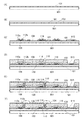
図1(A)は、本発明の一形態による発光装置の上面図であり、図1(B)は、図1(A)のA1−A2間の断面図である。
(Embodiment 1)
<Configuration of light emitting device>
FIG. 1A is a top view of a light-emitting device according to one embodiment of the present invention, and FIG. 1B is a cross-sectional view taken along line A1-A2 in FIG.
図1(A)に示す発光装置は、端子部4501、画素部4502、及び信号線回路部4503を有する。
A light-emitting device illustrated in FIG. 1A includes a
図1(B)に示すように、発光装置は、画素部4502に、第3基板903、第2接着層172、剥離層101、バッファ層103、複数のトランジスタ、絶縁層114、平坦化層116、発光素子130、隔壁124、第1接着層171、第2基板902を有する。
As illustrated in FIG. 1B, the light-emitting device includes a
図1(B)に示すように、第3基板903上に複数のトランジスタが備わっており、トランジスタ150及びトランジスタ151の上部には、それぞれ発光素子130が備わっている。各トランジスタは、ゲート電極層106、ソース電極層112a及びドレイン電極層112b、半導体層110、及びゲート絶縁層108を備える。トランジスタ150及びトランジスタ151は発光素子を駆動するトランジスタである。発光素子130は、その下部に位置するトランジスタに電気的に接続される。発光素子130は、平坦化層116上に配され、発光素子130の第1電極層118は、平坦化層116に備わったコンタクトホールを介してトランジスタに電気的に接続されている。発光素子130は、第1接着層171及び第2基板902によって封止される。第2基板902の内側面に、後述するタッチセンサを複数有し、発光装置がタッチパネルを備えてもよい。
As shown in FIG. 1B, a plurality of transistors are provided over the
本実施の形態では、トップエミッション構造(上面射出構造)の発光装置について例示するが、ボトムエミッション構造(下面射出構造)やデュアルエミッション構造(両面射出構造)としてもよい。 In this embodiment, a light-emitting device having a top emission structure (top emission structure) is illustrated, but a bottom emission structure (bottom emission structure) or a dual emission structure (double emission structure) may be used.
発光素子130は、トランジスタに電気的に接続された第1電極層118と、第1電極層118上の有機化合物を含む層120と、有機化合物を含む層120上の第2電極層122と、を有する。第1電極層118の端部は、隔壁124で覆われている。第2電極層122は、画素部4502の全面に渡って形成されている。
The light-emitting
図1(B)に示すように、発光装置は、信号線回路部4503に、トランジスタ152を有する。
As shown in FIG. 1B, the light-emitting device includes a
図1(B)に示すように、発光装置は、端子部4501に、導電層915、バンプ4556、異方性導電膜4519、及びFPC(Flexible Printed Circuit)4518を有する。FPC4518には、画素部4502の駆動及び制御のための各種電気部品が配されている。
As illustrated in FIG. 1B, the light-emitting device includes a
導電層915は、バンプ4556及び異方性導電膜4519を介して、FPC4518と電気的に接続する。なお、バンプ4556は設けなくてもよく、導電層915は、異方性導電膜4519と直接接することで、FPC4518と電気的に接続することが好ましい。
The
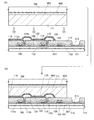
また、図7(A)は、本発明の別の形態による発光装置の上面図であり、図7(B)は、図7(A)のB1−B2間の断面図である。図7(A)では、第2基板902側に作製されるタッチパネルを詳細に示す。
7A is a top view of a light-emitting device according to another embodiment of the present invention, and FIG. 7B is a cross-sectional view taken along B1-B2 in FIG. 7A. FIG. 7A shows in detail a touch panel manufactured on the
図7(A)に示す発光装置は、端子部4501、画素部4502、及び信号線回路部4503を有する。
A light-emitting device illustrated in FIG. 7A includes a
図7(B)に示すように、発光装置は、画素部4502に、第3基板903、第2接着層172、剥離層101、バッファ層103、複数のトランジスタ、絶縁層114、平坦化層116、発光素子130、隔壁124、第1接着層171、オーバーコート層168、着色層166、遮光膜164、パッシベーション層163、絶縁層162、導電層の連結部911b、導電層の本体部912a、導電層920、絶縁層930及び第2基板902を有する。
7B, the light-emitting device includes a
図7(B)に示すように、第3基板903上に複数のトランジスタが備わっており、トランジスタ150及びトランジスタ151の上部には、それぞれ発光素子130が備わっている。トランジスタ及び発光素子の構成は図1(B)と同様である。
As shown in FIG. 7B, a plurality of transistors are provided over the
図7(B)に示すように、第2基板902側には、導電層の連結部911b及び導電層の本体部912aと、導電層の連結部911b及び導電層の本体部912aを覆う絶縁層930と、複数の導電層の本体部912aを電気的に接続する導電層920と、を有する。導電層920上に着色層166等を設けるため、導電層920と着色層166の間の絶縁層162は平坦化機能を有することが好ましい。また、パッシベーション層163は有していなくてもよい。
As shown in FIG. 7B, on the
図7(B)に示すように、発光装置は、信号線回路部4503に、トランジスタ152を有する。
As illustrated in FIG. 7B, the light-emitting device includes a
図7(B)に示すように、発光装置は、端子部4501に、導電層915、バンプ4556、ディスプレイ駆動用IC511、異方性導電膜4519、及びFPC4518を有する。
As illustrated in FIG. 7B, the light-emitting device includes a
導電層915は、バンプ4556及び異方性導電膜4519を介して、FPC4518と電気的に接続する。なお、バンプ4556は設けなくてもよく、導電層915は、異方性導電膜4519と直接接することで、FPC4518と電気的に接続することが好ましい。また、導電層915は、バンプ4556を介して、ディスプレイ駆動用IC511と電気的に接続する。なお、バンプ4556は設けなくてもよく、導電層915は、ディスプレイ駆動用IC511と直接接することが好ましい。導電層915を介して、ディスプレイ駆動用IC511とFPC4518は電気的に接続する。
The
第3基板903上には、画素部4502の周囲に沿って、データライン914が形成されている(図7(A))。データライン914は、第2基板902の内側面に形成された導電層911と導電層912で発生した電気的信号を、FPC4518に伝達する役割を行う。
A
第3基板903上の複数個の接続部512は、第2基板902に形成されている導電層911の接続部911d及び導電層912の接続部912dと対応する位置にそれぞれ形成される。そして、複数個の接続部512と、接続部911d,912dは、導電性部材によって電気的に接続される。このとき、導電性部材としては、銀ペーストなど、多様な導電性物質を用いることができる。一方、接続部512は、それぞれデータライン914と電気的に接続されており、データライン914は、FPC4518と電気的に接続される。
The plurality of
FPC4518には、第2基板902の内側面に形成された導電層911、912、920で発生した電気的信号が入力される、タッチパネルを駆動及び制御するためのタッチパネル駆動用IC913が配されている。
The
以下では、本発明の一実施形態に係る発光装置におけるタッチパネルの駆動方法について簡略に説明する。なお、本明細書中では、被検知体の近接又は接触を検知可能なセンサをタッチセンサと呼び、タッチパネルは、タッチセンサを複数有する。 Hereinafter, a method for driving the touch panel in the light emitting device according to an embodiment of the present invention will be briefly described. Note that in this specification, a sensor capable of detecting the proximity or contact of a detection target is referred to as a touch sensor, and the touch panel includes a plurality of touch sensors.
本発明の一態様の発光装置は、発光装置の表面に指、導電性物体又は高誘電率の物体が接近ないし接触した場合、このような接近によって引き起こされた導体の静電容量の変化を解釈してタッチを感知する。このとき、表面に近接又は接触した物体の座標(及びその押す圧力値)が出力される。 In the light-emitting device of one embodiment of the present invention, when a finger, a conductive object, or a high dielectric constant object approaches or contacts the surface of the light-emitting device, the change in the capacitance of the conductor caused by the approach is interpreted. To detect touch. At this time, the coordinates of the object close to or in contact with the surface (and the pressing pressure value) are output.
タッチセンサは、一対の電極を備え、これらの間に容量が形成される。一対の電極のうち、一方の電極に入力電圧が入力される。また、他方の電極に流れる電流(又は、他方の電極の電位)が検出回路により検出される。図7(A)(B)では、タッチセンサの一対の電極として、導電層911及び導電層912を用いる例を示したが、タッチセンサの一対の電極として、第2基板902側の電極(導電層911、導電層912の少なくとも一方)と、第2電極層122と、を用いてもよい。
The touch sensor includes a pair of electrodes, and a capacitor is formed between them. An input voltage is input to one of the pair of electrodes. Further, the current flowing through the other electrode (or the potential of the other electrode) is detected by the detection circuit. 7A and 7B illustrate an example in which the
画素部4502の第2電極層122には、定電圧としてのカソード電圧が印加されている。本発明の一態様の発光装置は、第2基板902側の電極及び第2電極層122で1つのキャパシタを形成できる。第2基板902側の電極及び第2電極層122の間の静電容量は一定に維持される。この状態で、第2基板902の上側表面に、指、導電性物体又は高誘電率の物体が接近ないし接触すれば、指等と第2基板902側の電極とが、第2のキャパシタを形成することになる。従って、全体的に見たとき、2つのキャパシタが直列に接続されている形態をなすことになり、全体的な静電容量に変化が生じることになる。かかる静電容量の変化が発生した位置及び大きさを利用し、タッチ感知システムが作動することになる。
A cathode voltage as a constant voltage is applied to the
<発光装置を構成する部材>
以下に本発明の一態様の発光装置を構成する部材について、説明する。
<Members constituting the light emitting device>
The members constituting the light-emitting device of one embodiment of the present invention are described below.
(第3基板)
第3基板903には、熱を加えられても変形の少ない熱膨張係数が10ppm/K以下の基板を用いることが好ましい。第3基板903に熱を加えても、第3基板903に接する樹脂や配線にクラックが生じにくいからである。第3基板903に使用できる材料は、例えば、ポリエチレンテレフタレート樹脂、ポリエチレンナフタレート樹脂、ポリアクリルニトリル樹脂、ポリイミド樹脂、ポリメチルメタクリレート樹脂、ポリカーボネート樹脂、ポリエーテルスルフォン樹脂、ポリアミド樹脂、ポリスチレン樹脂、ポリアミドイミド樹脂、ポリ塩化ビニル樹脂などを好適に用いることができる。
(Third substrate)
As the
(剥離層)
剥離層101は第1基板901とトランジスタ150の間に形成されている。剥離層101はタングステン、モリブデン、チタン、タンタル、ニオブ、ニッケル、コバルト、ジルコニウム、ルテニウム、ロジウム、パラジウム、オスミウム、イリジウム、シリコンから選択された元素、又は該元素を含む合金材料、又は該元素を含む化合物材料の少なくとも一つからなり、単層又は積層された層である。シリコンを含む層の結晶構造は、非晶質、微結晶、多結晶のいずれの場合でもよい。また、酸化アルミニウム、酸化ガリウム、酸化亜鉛、二酸化チタン、酸化インジウム、酸化インジウムスズ、酸化インジウム亜鉛、及びIn−Ga−Zn系金属酸化物等の金属酸化物のいずれかを用いてもよい。
(Peeling layer)
The
剥離層101が単層構造の場合、好ましくは、タングステン層、モリブデン層、又はタングステンとモリブデンの混合物を含む層を形成する。又は、タングステンの酸化物若しくは酸化窒化物を含む層、モリブデンの酸化物若しくは酸化窒化物を含む層、又はタングステンとモリブデンの混合物の酸化物若しくは酸化窒化物を含む層を形成する。なお、タングステンとモリブデンの混合物とは、例えば、タングステンとモリブデンの合金に相当する。
In the case where the
また、剥離層101として、タングステンを含む層とタングステンの酸化物を含む層の積層構造を形成する場合、タングステンを含む層を形成し、その上層に酸化物で形成される絶縁層を形成することで、タングステン層と絶縁層との界面に、タングステンの酸化物を含む層が形成されることを活用してもよい。また、タングステンを含む層の表面を、熱酸化処理、酸素プラズマ処理、オゾン水等の酸化力の強い溶液での処理等を行ってタングステンの酸化物を含む層を形成してもよい。
In the case where a stacked structure of a layer containing tungsten and a layer containing an oxide of tungsten is formed as the
本実施の形態では、第3基板903と剥離層101とが第2接着層172を介して貼り合わされている例を示したが、本発明の一態様の発光装置は、剥離層101を備えていなくてもよい。例えば、第3基板903とバッファ層103が第2接着層172を介して貼り合わされていてもよい。
In this embodiment, the example in which the
なお、本実施の形態では、トップエミッション構造の発光装置を例示するため、剥離層101の透光性は問わないが、ボトムエミッション構造やデュアルエミッション構造の発光装置が剥離層101を有する場合は、剥離層101に透光性を有する材料を用いる。
Note that in this embodiment mode, the light-emitting device having a top emission structure is illustrated, and thus the light-transmitting property of the
(第2基板)
第2基板902には、厚さが10μm以上500μm以下のガラスを用いることが好ましい。その厚さにすると、軽く、可撓性を持たせることができる。
(Second board)
For the
(バッファ層)
バッファ層103の材料は、酸化シリコン膜、酸化ガリウム膜、酸化ハフニウム膜、酸化イットリウム膜、若しくは酸化アルミニウム膜などの酸化絶縁膜、又は、窒化シリコン膜、若しくは窒化アルミニウム膜などの窒化絶縁膜、又は、酸化窒化シリコン膜、若しくは酸化窒化アルミニウム膜などの酸化窒化絶縁膜、又は、窒化酸化シリコン膜などの窒化酸化絶縁膜から選ばれた一の絶縁膜、又は、複数が積層された絶縁膜で形成できる。なお、「窒化酸化シリコン」とは、その組成として、酸素よりも窒素の含有量が多いものをいい、「酸化窒化シリコン」とは、その組成として、窒素よりも酸素の含有量が多いものをいう。
(Buffer layer)
The material of the
(ゲート電極層)
ゲート電極層106の材料は、モリブデン、チタン、タンタル、タングステン、アルミニウム、銅、クロム、ネオジム、スカンジウム等の金属材料又はこれらを主成分とする合金材料を用いて形成することができる。また、ゲート電極層106としてリン等の不純物元素をドーピングした多結晶シリコン膜に代表される半導体膜、ニッケルシリサイドなどのシリサイド膜を用いてもよい。ゲート電極層106は、単層構造としてもよいし、積層構造としてもよい。
(Gate electrode layer)
The material of the
(ゲート絶縁層)
ゲート絶縁層108の材料は、酸化シリコン膜、酸化ガリウム膜、酸化ハフニウム膜、酸化イットリウム膜、若しくは酸化アルミニウム膜などの酸化絶縁膜、又は、窒化シリコン膜、若しくは窒化アルミニウム膜などの窒化絶縁膜、又は、酸化窒化シリコン膜、若しくは酸化窒化アルミニウム膜などの酸化窒化絶縁膜、又は、窒化酸化シリコン膜などの窒化酸化絶縁膜から選ばれた一の絶縁膜、又は、複数が積層された絶縁膜で形成できる。
(Gate insulation layer)
A material of the
ゲート絶縁層108は、プラズマCVD(Chemical Vapor Deposition)法やスパッタリング法で形成する。プラズマCVD法を用いる場合、特にマイクロ波の電界エネルギーを利用してプラズマを発生させ、プラズマによりゲート絶縁膜の原料ガスを励起させ、励起させた原料ガスを被形成物上で反応させて反応物を堆積させるプラズマCVD法(マイクロ波プラズマCVD法ともいう。)を用いて形成することが好ましい。ゲート絶縁層108の膜厚は、5nm以上300nm以下とする。
The
(半導体層)
半導体層110はシリコン又は酸化物半導体を用いることができる。当該発明の作製方法において、第1基板901上に半導体層110を形成する。そのため、半導体層110を500℃以上の温度で成膜、又はアニール処理を行うことができる。そのため、電界効果移動度、オン電流の高いトランジスタを作製することができる。なお、当該半導体層110に用いることができる酸化物半導体の詳細は実施の形態2で説明する。
(Semiconductor layer)
The
(ソース電極層及びドレイン電極層)
ソース電極層112a及びドレイン電極層112bに用いる導電膜としては、例えば、Al、Cr、Cu、Ta、Ti、Mo、Wから選ばれた元素を含む金属膜、又は上述した元素を含む金属窒化物膜(窒化チタン膜、窒化モリブデン膜、窒化タングステン膜)等を用いることができる。また、Al、Cuなどの金属膜の下側又は上側の一方又は双方にTi、Mo、Wなどの高融点金属膜又はそれらの金属窒化物膜(窒化チタン膜、窒化モリブデン膜、窒化タングステン膜)を積層させた構成としても良い。また、ソース電極層112a及びドレイン電極層112bに用いる導電膜としては、導電性の金属酸化物で形成しても良い。導電性の金属酸化物としては酸化インジウム(In2O3等)、酸化スズ(SnO2等)、酸化亜鉛(ZnO)、インジウム錫酸化物(ITO)、インジウム亜鉛酸化物(In2O3―ZnO等)、又はこれらの金属酸化物材料に酸化シリコンを含ませたものを用いることができる。
(Source electrode layer and drain electrode layer)
As the conductive film used for the
(絶縁層)
絶縁層114は、プラズマCVD法を用いて、シラン(SiH4)と窒素(N2)の混合ガスを供給して成膜する窒化シリコン膜を用いることが好ましい。また、絶縁層114は、ゲート絶縁層108と同様の材料を用いて形成してもよい。
(Insulating layer)
The insulating
(平坦化層)
平坦化層116は、ポリイミド樹脂又はアクリル樹脂などの有機樹脂材料又は、酸化シリコン等の無機絶縁材料で形成することができる。
(Flattening layer)
The
(発光素子)
発光素子130は、第1電極層118と第2電極層122に挟持された有機化合物を含む層120を有する。有機化合物を含む層120は、少なくとも発光層を含むものであり、複数の層を有する。有機化合物を含む層120については実施の形態3で説明する。
(Light emitting element)
The
本実施の形態では、トップエミッション構造の発光装置について例示するため、第2電極層122には、可視光を透過する導電膜を用いる。第1電極層118には、可視光を反射する導電膜を用いることが好ましい。なお、第1電極層118と第2電極層122は、一方が陽極として機能し、他方が陰極として機能する。
In this embodiment mode, a conductive film that transmits visible light is used for the
可視光を透過する導電膜は、例えば、酸化インジウム、ITO、インジウム亜鉛酸化物、ZnO、ガリウムを添加したZnOなどを用いて形成することができる。また、金、白金、ニッケル、タングステン、クロム、モリブデン、鉄、コバルト、銅、パラジウム、もしくはチタン等の金属材料、又はこれら金属材料の窒化物(例えば、窒化チタン)等も、透光性を有する程度に薄く形成することで用いることができる。また、グラフェン等を用いても良い。 The conductive film that transmits visible light can be formed using, for example, indium oxide, ITO, indium zinc oxide, ZnO, ZnO to which gallium is added, or the like. In addition, a metal material such as gold, platinum, nickel, tungsten, chromium, molybdenum, iron, cobalt, copper, palladium, or titanium, or a nitride of these metal materials (for example, titanium nitride) has a light-transmitting property. It can be used by forming it as thin as possible. Further, graphene or the like may be used.
可視光を反射する導電膜は、例えば、アルミニウム、金、白金、銀、ニッケル、タングステン、クロム、モリブデン、鉄、コバルト、銅、もしくはパラジウム等の金属材料、アルミニウムとチタンの合金、アルミニウムとニッケルの合金、アルミニウムとネオジムの合金等のアルミニウムを含む合金(アルミニウム合金)、又は、銀と銅の合金等の銀を含む合金を用いて形成することができる。銀と銅の合金は、耐熱性が高いため好ましい。また、上記金属材料や合金に、ランタン、ネオジム、又はゲルマニウム等が添加されていても良い。 The conductive film that reflects visible light is, for example, a metal material such as aluminum, gold, platinum, silver, nickel, tungsten, chromium, molybdenum, iron, cobalt, copper, or palladium, an alloy of aluminum and titanium, or aluminum and nickel. An alloy, an alloy containing aluminum such as an alloy of aluminum and neodymium (aluminum alloy), or an alloy containing silver such as an alloy of silver and copper can be used. An alloy of silver and copper is preferable because of its high heat resistance. In addition, lanthanum, neodymium, germanium, or the like may be added to the metal material or alloy.
第1電極層118に可視光を反射する導電膜を用いることで、発光素子からの光の取り出し効率を向上でき、好ましい。
It is preferable to use a conductive film that reflects visible light for the
(隔壁)
隔壁124は、無機絶縁材料、又は有機絶縁材料を用いて形成することができる。例えば、有機絶縁材料としては、ネガ型やポジ型の感光性を有する樹脂材料、非感光性の樹脂材料などを用いることができ、具体的には、ポリイミド樹脂、又はアクリル樹脂等で形成することができる。
(Partition wall)
The
(着色層、遮光膜、オーバーコート層)
着色層166は、特定の波長帯域の光を透過する有色層である。例えば、赤色の波長帯域の光を透過する赤色(R)のカラーフィルタ、緑色の波長帯域の光を透過する緑色(G)のカラーフィルタ、青色の波長帯域の光を透過する青色(B)のカラーフィルタなどを用いることができる。各カラーフィルタは、公知の材料を用いて、印刷法、インクジェット法、フォトリソグラフィー法を用いたエッチング方法などでそれぞれ所望の位置に形成する。
(Colored layer, light shielding film, overcoat layer)
The
なお、ここでは、RGBの3色を用いた方法について説明したが、これに限定されず、RGBY(黄色)等の4色を用いた構成、又は、5色以上の構成としてもよい。 Although a method using three colors of RGB has been described here, the present invention is not limited to this, and a configuration using four colors such as RGBY (yellow) or a configuration of five or more colors may be used.
遮光膜164は隣接する画素の発光素子130からの光を遮光し、隣接する画素間における混色を抑制する。ここで、着色層166の端部を、遮光膜164と重なるように設けることにより、光漏れを抑制することができる。遮光膜164は、発光素子130からの発光を遮光する材料を用いることができ、金属や、有機樹脂などの材料を用いて形成することができる。なお、遮光膜164やオーバーコート層168は、画素部4502にのみ設けてもよいし、信号線回路部4503などの画素部4502以外の領域にまで設けてもよい。
The
絶縁層162には、平坦化層116と同様の材料を用いることができる。また、パッシベーション層163には、ゲート絶縁層108等に用いることができる無機絶縁材料を適用できる。
For the insulating
オーバーコート層168は、アクリル樹脂、ポリイミド樹脂等の有機樹脂膜により形成することができる。オーバーコート層168により、着色層166に含有された不純物成分等を有機化合物を含む層120側への拡散を防止することができる。また、オーバーコート層168は、有機樹脂膜と無機絶縁膜との積層構造としてもよい。無機絶縁膜としては、窒化シリコン、酸化シリコンなどを用いることができる。なお、オーバーコート層168は、設けない構成としてもよい。
The
(第1接着層)
第1接着層171は、第2電極層122と第2基板902との間に設けられ、第2基板902と第3基板903を接着する。第1接着層171としては、光硬化型の接着剤、反応硬化型接着剤、熱硬化型接着剤、又は嫌気型接着剤を用いることができる。例えば、エポキシ樹脂、アクリル樹脂、イミド樹脂等を用いることができる。また、接着剤に光の波長以下の大きさの乾燥剤(ゼオライト等)や、屈折率の大きいフィラー(酸化チタンや、ジルコニウム等)を混合することにより、発光素子130の信頼性が向上、又は発光素子130からの光取り出し効率が向上するため好適である。
(First adhesive layer)
The first
(第2接着層)
第2接着層172は、第1接着層171と同様の材料を用いることができる。
(Second adhesive layer)
The second
(タッチパネル)
以下では、本発明の一態様に係る発光装置において、第2基板902の一面に形成されているタッチパネルについて説明する。
(Touch panel)
Hereinafter, a touch panel formed over one surface of the
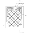
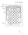
図8及び図9はそれぞれ、図7の発光装置の第2基板902及びその一面上に形成されている導電層911及び導電層912を示す上面図である。図10は、図7の発光装置の第2基板902及びその一面上に形成されている導電層911、導電層912及び導電層920を示す上面図である。図11は、図10のC1−C2間の断面図である。図12は、図7の発光装置の第2基板902及びその一面上に形成されている導電層911、導電層912及び導電層920を示す斜視図である。
8 and 9 are top views showing the
第2基板902の第3基板903と対向する面には、導電層911、導電層912、絶縁層930、及び導電層920が順に形成されている。
A
本発明の一実施形態に係る発光装置は、発光装置の第2基板902の内側面に、タッチパネル機能の発現のための導電層としてITO膜を形成している。
In the light emitting device according to an embodiment of the present invention, an ITO film is formed on the inner surface of the
導電層911及び導電層912は、第2基板902の第3基板903と対向する面に複数形成される。導電層911は、第1方向(図8のX方向)に沿って互いに並んで形成され、複数の本体部912aを有する導電層912は、第1方向と実質的に垂直である第2方向(図9のY方向)に沿って互いに並んで形成される。図8及び図9に図示されているように、導電層911及び導電層912は、交互に配される。すなわち、第2基板902上には、複数個の導電層911が第1方向(図8のX方向)に沿って互いに並んで形成されており、このような複数個の導電層911間に、複数個の導電層912が第2方向(図9のY方向)に沿って互いに並んで形成されている。
A plurality of the
ここで、1つの導電層911を図8のパターン1000に示す。導電層911は、それぞれ複数個の本体部911a、複数個の連結部911b、1つの延長部911c及び1つの接続部911dを含む。本体部911aはほぼ菱形状(正方形)に形成され、第1方向、例えば、図8のX方向に沿って複数個が一列に形成されている。連結部911bは、互いに隣接している本体部911a間に形成され、互いに隣接している本体部911a間を連結する役割を担う。延長部911cは、導電層の本体部911a一端部から延長して形成されている。複数個の導電層911では、すべての延長部911cが同一方向、例えば、図8のY方向に延び、各延長部911cがいずれも第2基板902の一端部、すなわち、図8で見たとき、上側に集まるように形成されうる。そして、延長部911cの端部には、接続部911dが形成されている。接続部911dは、後述する導電性部材を介して、第3基板903のデータライン914に電気的に接続される。
Here, one
一方、1つの導電層912を図9のパターン2000に示す。導電層912は、それぞれ複数個の本体部912a、1つの延長部912c及び1つの接続部912dを含む。本体部912aは、ほぼ菱形状(正方形)に形成されており、第2方向、例えば、図9のY方向に沿って、複数個が一列に形成されている。ここで、前述の導電層911とは異なり、導電層912は連結部を含まず、従って、それぞれの本体部912aが、互いに連結されていない場合がある。このとき、それぞれの本体部912aは、後述する導電層920によって互いに連結される。一方、延長部912cは、導電層の本体部912a一端部から延長して形成されている。複数個の導電層912では、すべての延長部912cが、同一方向、例えば、図9のY方向に延び、各延長部912cがいずれも第2基板902の一端部、すなわち、図9で見たとき、上側に集まるように形成されうる。そして、延長部912cの端部には、接続部912dが形成されている。接続部912dは、後述する導電性部材を介して、第3基板903のデータライン914に電気的に接続される。
On the other hand, one
図11及び図12に示すように、絶縁層930は、第2基板902の第3基板903と対向する面に、導電層911、912を覆うように形成する。絶縁層930は、導電層911、912と導電層920とを絶縁させる役割を担う。そして、絶縁層930の所定の位置、例えば、導電層912の本体部912aの互いに対面している端部付近には、コンタクトホール931が形成されうる。コンタクトホール931を介して、導電層912の本体部912aと導電層920とが互いに連結される。
As shown in FIGS. 11 and 12, the insulating
図10ないし図12に図示されているように、導電層920は、絶縁層930の第3基板903と対向する面に形成される。このとき、導電層920は、絶縁層930のコンタクトホール931を充填するように形成され、導電層912の互いに隣接している本体部912a間を電気的に接続する役割を行う。
As shown in FIGS. 10 to 12, the
かかる構成を介して、互いに直交する方向に形成されている導電層911と導電層912とを互いに交差させないようにできる。そのため、導電層911と導電層912との間の電気的短絡を防止することができる。
Through such a configuration, the
ここで、導電層911、912、920は、例えば、酸化インジウム(In2O3等)、酸化スズ(SnO2等)、ZnO、ITO、インジウム亜鉛酸化物、又はこれらの金属酸化物材料に酸化シリコンを含ませたものから形成できる。そして、かかる導電層911、912、920は、フォトリソグラフィー工程を行って形成できる。すなわち、蒸着、スピンコーティング、スパッタリング、インクジェットのような方法を使用して形成されたITO層をパターニングし、導電層911、912、920を形成できる。また、絶縁層930は、ゲート絶縁層108と同様の無機絶縁材料を用いて形成できる。
Here, the
上記構成により、第2基板902の内側面に導電層911、導電層912、導電層920、及び絶縁層930を形成することができる。そのため、タッチパネルを有し、かつ、薄く可撓性を有する発光装置を作製することができる。
With the above structure, the
<発光装置の作製方法>
図2乃至図6に本発明の一態様の発光装置の作製方法を示す。以下に述べる各構成要素を構成する材料は、上記を参酌できるものとする。
<Method for Manufacturing Light-Emitting Device>
2A to 6B illustrate a method for manufacturing a light-emitting device of one embodiment of the present invention. The material constituting each component described below can take the above into consideration.
まず、第1基板901上に剥離層101を形成する(図2(A))。第1基板901としては、ガラス基板、石英基板、サファイア基板、セラミック基板、金属基板などを用いることができる。剥離層101は、前述の材料を用いて、スパッタリング法やプラズマCVD法、塗布法、印刷法、蒸着法等で形成することができる。なお、塗布法はスピンコーティング法、液滴吐出法、ディスペンス法を含む。
First, the
次に、剥離層101上にバッファ層103を形成する(図2(B))。バッファ層103は、窒化珪素膜や酸化窒化珪素膜、窒化酸化珪素膜などの窒素と珪素を含む絶縁層を、プラズマCVD法により成膜温度を250℃〜400℃として形成することで、緻密で非常に透水性の低い層とすることができる。
Next, the
次に、バッファ層103上に導電膜を形成し、導電膜を選択的にエッチングすることでゲート電極層106を形成する。次に、ゲート電極層106に接するように、ゲート絶縁層108を形成する。次に、半導体層110を形成する。半導体層110はスパッタリング法、プラズマCVD法等により成膜することができる。次に、導電膜をスパッタリング法により形成する。この導電膜を選択的にエッチングして、ソース電極層112a及びドレイン電極層112b、並びに導電層915を形成する(図2(C))。
Next, a conductive film is formed over the
次に、絶縁層114を、半導体層110、ソース電極層112a及びドレイン電極層112bと接するように形成する。次に平坦化層116を絶縁層114上に形成する(図2(D))。平坦化層116と絶縁層114には開口を設ける。これにより、トランジスタのソース電極層112a又はドレイン電極層112bと後に形成する第1電極層118を電気的に接続できる。また、後に、導電層915と、異方性導電膜4519や、バンプ4556、FPC4518等とを電気的に接続できる。
Next, the insulating
次に、導電膜を形成し、導電膜を選択的にエッチングすることで第1電極層118を形成する(図2(E))。
Next, a conductive film is formed, and the
次に、隔壁124を、第1電極層118の端部を覆うように形成する。隔壁124は、隣接する第1電極層118を電気的に絶縁する(図2(F))。また、隔壁124は、その上面に形成される膜が途切れないように、順テーパ形状を有していることが好ましい。なお、順テーパ形状とは、下地となる層に他の層がなだらかな角度で厚みを増して接する構成を言う。
Next, the
次に、蒸着法により有機化合物を含む層120を第1電極層118と隔壁124に接するように形成する(図3(A))。有機化合物を含む層120に高分子材料を用いる場合は、塗布法により形成することもできる。
Next, a
次に、有機化合物を含む層120に接するように、第2電極層122を形成する(図3(B))。第2電極層122は、蒸着法、又はスパッタリング法で形成することができる。
Next, the
以上の工程により、トランジスタ150の上に、発光素子130を形成することができる。第1基板901上にトランジスタ150と発光素子130が形成された基板を、バックプレーン基板1と呼ぶことにする。
Through the above steps, the light-emitting
次に、支持基板700に吸着層600を形成する(図4(A))。支持基板700として、厚さが0.5mm以上1mm以下のガラスを用いることが好ましい。吸着層600は、製造工程における加熱や化学処理に対する耐久性がある。吸着層600として使用する接着材料は、白金系触媒を含んだシリコーン樹脂が好ましい。
Next, the
次に、吸着層600に接するように、第2基板902を貼り付ける(図4(B))。支持基板700に吸着層600を介して第2基板902を貼り付けた基板を対向基板2と呼ぶ。支持基板700は、吸着層600により第2基板902と接着されている。なお、後の工程で、支持基板700は、第2基板902から剥離することができる。
Next, the
次に、バックプレーン基板1と対向基板2を貼り付ける工程を行う。まず、対向基板2の第2基板902の表面に、第1接着層171を塗る(図4(C))。
Next, a process of attaching the
次に、第1接着層171を塗った面に、バックプレーン基板1の発光素子130等が設けられた面を貼り合わせる(図5(A)及び図5(B))。
Next, the surface provided with the light-emitting
第1接着層171が硬化したのち、第1基板901を剥離し(図6(A))、第2接着層172を用いて第3基板903を剥離層101(又はバッファ層103)に貼り付ける(図6(B))。
After the first
第3基板903への転置工程は、様々な方法を適宜用いることができる。例えば、剥離層101として、被剥離層と接する側に金属酸化膜を含む層を形成した場合は、当該金属酸化膜を結晶化により脆弱化して、被剥離層を作製基板から剥離することができる。また、耐熱性の高い作製基板と被剥離層の間に、剥離層として水素を含む非晶質珪素膜を形成した場合はレーザ光の照射又はエッチングにより当該非晶質珪素膜を除去することで、被剥離層を作製基板から剥離することができる。また、剥離層として、被剥離層と接する側に金属酸化膜を含む層を形成し、当該金属酸化膜を結晶化により脆弱化し、さらに剥離層の一部を溶液やNF3、BrF3、ClF3等のフッ化ガスを用いたエッチングで除去した後、脆弱化された金属酸化膜において剥離することができる。さらには、剥離層101として窒素、酸素や水素等を含む膜(例えば、水素を含む非晶質珪素膜、水素含有合金膜、酸素含有合金膜など)を用い、剥離層にレーザ光を照射して剥離層101内に含有する窒素、酸素や水素をガスとして放出させ被剥離層と基板との剥離を促進する方法を用いても良い。
Various methods can be used as appropriate for the transfer step to the
又は、被剥離層が形成された作製基板を機械的に削除又は溶液やNF3、BrF3、ClF3等のフッ化ガスによるエッチングで除去する方法等を用いることができる。この場合、剥離層を設けなくとも良い。 Alternatively, a method in which a manufacturing substrate over which a layer to be peeled is formed is mechanically deleted or removed by etching with a solution or a fluorinated gas such as NF 3 , BrF 3 , or ClF 3 can be used. In this case, it is not necessary to provide a release layer.
また、上記剥離方法を複数組み合わせることでより容易に転置工程を行うことができる。つまり、レーザ光の照射、ガスや溶液などによる剥離層へのエッチング、鋭いナイフやメスなどによる機械的な削除を行い、剥離層と被剥離層とを剥離しやすい状態にしてから、物理的な力(機械等による)によって剥離を行うこともできる。 Moreover, the transposition process can be performed more easily by combining a plurality of the above peeling methods. In other words, laser beam irradiation, etching of the release layer with gas or solution, mechanical deletion with a sharp knife or scalpel, etc., make the release layer and the release layer easy to peel off, and then physically Peeling can also be performed by force (by machine or the like).
その他の剥離方法としては、剥離層101をタングステンで形成した場合は、アンモニア水と過酸化水素水の混合溶液により剥離層101をエッチングしながら剥離を行うと良い。
As another peeling method, in the case where the
上記の工程によりトランジスタ150と発光素子130を、第1基板901から軽量で可撓性のある第3基板903に転置することができた。
Through the above steps, the
次に、支持基板700を上記発光装置から、剥離する(図6(C))。剥離法は、例えば、支持基板700と第2基板902の間にある吸着層600に鋭利な刃物で切り込みをいれ、第2基板902から支持基板700を剥離すればよい。
Next, the
本発明の一態様の発光装置の作製方法により、第2基板902と、第3基板903で発光装置を作製することができる。第2基板902は、厚さが10μm以上500μm以下のガラスであるので、発光装置の重量を軽くすることができる。また、第3基板903は樹脂であるので、可撓性を有する発光装置を得ることができる。
With the method for manufacturing a light-emitting device of one embodiment of the present invention, a light-emitting device can be manufactured using the
以下では、図7(A)(B)の構成を適用する場合の作製方法を、図4(D)を用いて示す。 Hereinafter, a manufacturing method in the case of applying the structure in FIGS. 7A and 7B will be described with reference to FIG.
第2基板902が吸着層600により支持基板700と接着している状態(図4(B))で、以下の工程を行う。
In a state where the
まず、第2基板902上に、導電層911及び導電層912を形成し、導電層911及び導電層912を覆う絶縁層930を形成した後、絶縁層930に開口を設け、導電層912の一部を露出させる。そして、絶縁層930及び導電層912上に導電層920を形成する。各構成については、先の説明を参酌することができる。
First, the
次に、導電層920を覆うように絶縁層162をCVD法、スパッタリング法等で形成する。次に、絶縁層162に接するようにパッシベーション層163を形成する。次に、フォトリソグラフィー工程を用いて遮光膜164を形成する。次に、フォトリソグラフィー工程を用いて、着色層166を形成する。次に、着色層166に接するように、オーバーコート層168を形成する。オーバーコート層168により、着色層166中に含まれる色素の熱拡散を防止することができる。
Next, the insulating
上記の工程により、第2基板902上に、タッチパネルやカラーフィルタ等を形成することができる。
Through the above process, a touch panel, a color filter, and the like can be formed over the
(実施の形態2)
本実施の形態では、実施の形態1における半導体層に用いることのできる酸化物半導体について詳細を説明する。
(Embodiment 2)
In this embodiment, an oxide semiconductor that can be used for the semiconductor layer in
上記酸化物半導体としては、例えばIn系金属酸化物、Zn系金属酸化物、In−Zn系金属酸化物、又はIn−Ga−Zn系金属酸化物などを適用できる。また、上記In−Ga−Zn系金属酸化物に含まれるGaの一部若しくは全部の代わりに他の金属元素を含む金属酸化物を用いてもよい。 As the oxide semiconductor, for example, an In-based metal oxide, a Zn-based metal oxide, an In—Zn-based metal oxide, an In—Ga—Zn-based metal oxide, or the like can be used. Alternatively, a metal oxide containing another metal element instead of part or all of Ga contained in the In—Ga—Zn-based metal oxide may be used.
上記他の金属元素としては、例えばガリウムよりも多くの酸素原子と結合が可能な金属元素を用いればよく、例えばチタン、ジルコニウム、ハフニウム、ゲルマニウム、及び錫のいずれか一つ又は複数の元素を用いればよい。また、上記他の金属元素としては、ランタン、セリウム、プラセオジム、ネオジム、サマリウム、ユウロピウム、ガドリニウム、テルビウム、ジスプロシウム、ホルミウム、エルビウム、ツリウム、イッテルビウム、及びルテチウムのいずれか一つ又は複数の元素を用いればよい。これらの金属元素は、スタビライザーとしての機能を有する。なお、これらの金属元素の添加量は、金属酸化物が半導体として機能することが可能な量である。ガリウムよりも多くの酸素原子と結合が可能な金属元素を用い、さらには金属酸化物中に酸素を供給することにより、金属酸化物中の酸素欠陥を少なくできる。 As the other metal element, for example, a metal element capable of bonding with more oxygen atoms than gallium may be used. For example, one or more elements of titanium, zirconium, hafnium, germanium, and tin are used. That's fine. As the other metal element, any one or more of lanthanum, cerium, praseodymium, neodymium, samarium, europium, gadolinium, terbium, dysprosium, holmium, erbium, thulium, ytterbium, and lutetium may be used. Good. These metal elements have a function as a stabilizer. Note that the added amount of these metal elements is an amount by which the metal oxide can function as a semiconductor. By using a metal element capable of bonding with more oxygen atoms than gallium, and further supplying oxygen into the metal oxide, oxygen defects in the metal oxide can be reduced.
また、In:Ga:Zn=1:1:1の原子比である第1の酸化物半導体層、In:Ga:Zn=3:1:2の原子比である第2の酸化物半導体層、及びIn:Ga:Zn=1:1:1の原子比である第3の酸化物半導体層の積層により、半導体層110を構成してもよい。上記積層により半導体層110を構成することで、例えばトランジスタの電界効果移動度を高めることができる。
A first oxide semiconductor layer having an atomic ratio of In: Ga: Zn = 1: 1: 1; a second oxide semiconductor layer having an atomic ratio of In: Ga: Zn = 3: 1: 2; Alternatively, the
また、上記酸化物半導体を、C Axis Aligned Crystalline Oxide Semiconductor(CAAC−OSともいう)としてもよい。 The oxide semiconductor may be C Axis Aligned Crystalline Oxide Semiconductor (also referred to as CAAC-OS).
CAAC−OSは、複数の結晶部を有する酸化物半導体の一つである。結晶部では、c軸が酸化物半導体層の被形成面の法線ベクトル又は表面の法線ベクトルに平行な方向に揃い、且つab面に垂直な方向から見て金属原子が三角形状又は六角形状に配列し、c軸に垂直な方向から見て金属原子が層状、又は金属原子と酸素原子が層状に配列している。なお、本明細書において、単に垂直と記載する場合、85°以上95°以下の範囲も含まれる。また、単に平行と記載する場合、−5°以上5°以下の範囲も含まれる。 The CAAC-OS is one of oxide semiconductors having a plurality of crystal parts. In the crystal part, the c-axis is aligned in a direction parallel to the normal vector of the surface where the oxide semiconductor layer is formed or the normal vector of the surface, and the metal atoms are triangular or hexagonal when viewed from the direction perpendicular to the ab plane. The metal atoms are arranged in layers, or the metal atoms and oxygen atoms are arranged in layers as viewed from the direction perpendicular to the c-axis. Note that in this specification, the term “perpendicular” includes a range of 85 ° to 95 °. In addition, a simple term “parallel” includes a range from −5 ° to 5 °.
例えば、多結晶である酸化物半導体スパッタリング用ターゲットを用いたスパッタリング法によってCAAC−OSを形成できる。スパッタリング用ターゲットにイオンが衝突すると、スパッタリング用ターゲットに含まれる結晶領域がa−b面から劈開し、a−b面に平行な面を有する平板状又はペレット状のスパッタリング粒子として剥離することがある。この場合、平板状のスパッタリング粒子が、結晶状態を維持したまま基板に到達することにより、スパッタリング用ターゲットの結晶状態が基板に転写される。これにより、CAAC−OSが形成される。 For example, the CAAC-OS can be formed by a sputtering method using a polycrystalline oxide semiconductor sputtering target. When ions collide with the sputtering target, the crystal region included in the sputtering target may be cleaved from the ab plane, and may be separated as flat or pellet-like sputtering particles having a plane parallel to the ab plane. . In this case, when the flat sputtered particles reach the substrate while maintaining the crystalline state, the crystalline state of the sputtering target is transferred to the substrate. Thereby, the CAAC-OS is formed.
また、CAAC−OSを形成するために、以下の条件を適用することが好ましい。 In order to form a CAAC-OS, it is preferable to apply the following conditions.
例えば、不純物濃度を低減してCAAC−OSを形成することにより、不純物による酸化物半導体の結晶状態の崩壊を抑制できる。例えば、成膜室内に存在する不純物(水素、水、二酸化炭素、及び窒素など)を低減することが好ましい。また、成膜ガス中の不純物を低減することが好ましい。例えば、成膜ガスとして露点が−80℃以下、好ましくは−100℃以下である成膜ガスを用いることが好ましい。 For example, when the CAAC-OS is formed with a reduced impurity concentration, collapse of the oxide semiconductor crystal state due to the impurities can be suppressed. For example, it is preferable to reduce impurities (such as hydrogen, water, carbon dioxide, and nitrogen) present in the deposition chamber. Further, it is preferable to reduce impurities in the deposition gas. For example, a film forming gas having a dew point of −80 ° C. or lower, preferably −100 ° C. or lower is preferably used as the film forming gas.
また、成膜時の基板加熱温度を高めることで、基板付着後にスパッタリング粒子のマイグレーションが起こる。具体的には、基板加熱温度を100℃以上740℃以下として成膜する。成膜時の基板加熱温度を高めることで、平板状のスパッタリング粒子が基板に到達した場合、基板上でマイグレーションし、平らな面を向けて基板に付着する。 Further, by increasing the substrate heating temperature during film formation, migration of the sputtered particles occurs after the substrate adheres. Specifically, the film is formed at a substrate heating temperature of 100 ° C. or higher and 740 ° C. or lower. By increasing the substrate heating temperature during film formation, when the flat sputtered particles reach the substrate, they migrate on the substrate and adhere to the substrate with the flat surface facing.
また、成膜ガス中の酸素割合を高め、電力を最適化して成膜時のプラズマダメージを軽減させることが好ましい。成膜ガス中の酸素割合は、30体積%以上、好ましくは100体積%とする。 In addition, it is preferable to reduce the plasma damage during the film formation by increasing the oxygen ratio in the film formation gas and optimizing the electric power. The oxygen ratio in the deposition gas is 30% by volume or more, preferably 100% by volume.
上記スパッタリング用ターゲットの一例として、In−Ga−Zn−O化合物ターゲットについて以下に示す。 As an example of the sputtering target, an In—Ga—Zn—O compound target is described below.
InOx粉末、GaOy粉末、及びZnOz粉末を所定の比率で混合し、加圧処理後、1000℃以上1500℃以下の温度で加熱処理をすることにより、多結晶であるIn−Ga−Zn−O化合物ターゲットを形成する。なお、x、y、及びzは任意の正数である。ここで、所定の比率は、例えば、InOx粉末、GaOy粉末、及びZnOz粉末が、2:2:1、8:4:3、3:1:1、1:1:1、4:2:3又は3:1:2のmol数比である。なお、粉末の種類、及びその混合する比率は、作製するスパッタリング用ターゲットによって適宜変更すればよい。 In-Ga-Zn that is polycrystalline by mixing InO x powder, GaO y powder, and ZnO z powder at a predetermined ratio, and after heat treatment at a temperature of 1000 ° C. to 1500 ° C. -O compound target is formed. Note that x, y, and z are arbitrary positive numbers. Here, the predetermined ratio is, for example, 2: 2: 1, 8: 4: 3, 3: 1: 1, 1: 1: 1, 4: InO x powder, GaO y powder, and ZnO z powder. The molar ratio is 2: 3 or 3: 1: 2. Note that the type of powder and the mixing ratio may be changed as appropriate depending on the sputtering target to be manufactured.
チャネル形成領域が上記CAAC−OSであるトランジスタは、可視光や紫外光の照射による電気特性の変動が低いため、信頼性が高い。 A transistor whose channel formation region is the CAAC-OS has high reliability because variation in electrical characteristics due to irradiation with visible light or ultraviolet light is low.
上記酸化物半導体を含むトランジスタは、バンドギャップが広いため熱励起によるリーク電流が少ない。さらに、正孔の有効質量が10以上と重く、トンネル障壁の高さが2.8eV以上と高い。これにより、トンネル電流が少ない。さらに、半導体層中のキャリアが極めて少ない。よって、オフ電流を低くできる。例えば、オフ電流は、室温(25℃)でチャネル幅1μmあたり1×10⁻¹⁹A(100zA)以下である。より好ましくは1×10⁻²²A(100yA)以下である。トランジスタのオフ電流は、低ければ低いほどよいが、トランジスタのオフ電流の下限値は、約1×10⁻³⁰A/μmであると見積もられる。 Since the transistor including the oxide semiconductor has a wide band gap, leakage current due to thermal excitation is small. Furthermore, the effective mass of holes is as heavy as 10 or more, and the height of the tunnel barrier is as high as 2.8 eV or more. Thereby, the tunnel current is small. Furthermore, there are very few carriers in the semiconductor layer. Thus, the off-state current can be reduced. For example, the off-state current is 1 × 10 −19 A (100 zA) or less per channel width of 1 μm at room temperature (25 ° C.). More preferably, it is 1 × 10 −22 A (100 yA) or less. The lower the off-state current of the transistor, the better. However, the lower limit value of the off-state current of the transistor is estimated to be about 1 × 10 −30 A / μm.
本実施の形態は、他の実施の形態に記載した構成と適宜組み合わせて実施することが可能である。 This embodiment can be implemented in appropriate combination with the structures described in the other embodiments.
(実施の形態3)
本実施の形態では、実施の形態1における発光素子130に適用できる構成例について詳細を説明する。
(Embodiment 3)
In this embodiment, a structural example that can be applied to the light-emitting
図13(A)に示す発光素子130は、一対の電極(第1電極層118、第2電極層122)間に有機化合物を含む層120が挟まれた構造を有する。なお、以下の本実施の形態の説明においては、例として、第1電極層118を陽極として用い、第2電極層122を陰極として用いるものとする。
A light-emitting
また、有機化合物を含む層120は、少なくとも発光層を含んで形成されていればよく、発光層以外の機能層を含む積層構造であっても良い。発光層以外の機能層としては、正孔注入性の高い物質、正孔輸送性の高い物質、電子輸送性の高い物質、電子注入性の高い物質、バイポーラ性の物質(電子及び正孔の輸送性の高い物質)等を含む層を用いることができる。具体的には、正孔注入層、正孔輸送層、電子輸送層、電子注入層等の機能層を適宜組み合わせて用いることができる。有機化合物を含む層120には、低分子系化合物及び高分子系化合物のいずれを用いることもでき、無機化合物を含んでいても良い。有機化合物を含む層120を構成する層は、それぞれ、蒸着法(真空蒸着法を含む)、転写法、印刷法、インクジェット法、塗布法等の方法で形成することができる。
Moreover, the
図13(A)に示す発光素子130は、第1電極層118と第2電極層122との間に生じた電位差により電流が流れ、有機化合物を含む層120において正孔と電子とが再結合し、発光するものである。つまり有機化合物を含む層120に発光領域が形成されるような構成となっている。
In the light-emitting
本発明において、発光素子130からの発光は、第1電極層118、又は第2電極層122側から外部に取り出される。従って、第1電極層118、又は第2電極層122のいずれか一方は透光性を有する物質で形成される。
In the present invention, light emitted from the
なお、有機化合物を含む層120は図13(B)のように第1電極層118と第2電極層122との間に複数積層されていても良い。n(nは2以上の自然数)層の積層構造を有する場合には、m(mは自然数、mは1以上n−1以下)番目の有機化合物を含む層120と、(m+1)番目の有機化合物を含む層120との間には、それぞれ電荷発生層120aを設けることが好ましい。
Note that a plurality of
電荷発生層120aは、有機化合物と金属酸化物の複合材料、金属酸化物、有機化合物とアルカリ金属、アルカリ土類金属、又はこれらの化合物との複合材料の他、これらを適宜組み合わせて形成することができる。有機化合物と金属酸化物の複合材料としては、例えば、有機化合物と酸化バナジウムや酸化モリブデンや酸化タングステン等の金属酸化物を含む。有機化合物としては、芳香族アミン化合物、カルバゾール誘導体、芳香族炭化水素等の低分子化合物、又は、それらの低分子化合物のオリゴマー、デンドリマー、ポリマー等など、種々の化合物を用いることができる。なお、有機化合物としては、正孔輸送性有機化合物として正孔移動度が10−6cm2/Vs以上であるものを適用することが好ましい。但し、電子よりも正孔の輸送性の高い物質であれば、これら以外のものを用いてもよい。なお、電荷発生層120aに用いるこれらの材料は、キャリア注入性、キャリア輸送性に優れているため、発光素子130の低電流駆動、及び低電圧駆動を実現することができる。
The
なお、電荷発生層120aは、有機化合物及び金属酸化物の複合材料と、他の材料とを組み合わせて形成してもよい。例えば、有機化合物及び金属酸化物の複合材料を含む層と、電子供与性物質の中から選ばれた一の化合物及び電子輸送性の高い化合物を含む層とを組み合わせて形成してもよい。また、有機化合物及び金属酸化物の複合材料を含む層と、透明導電膜とを組み合わせて形成してもよい。
Note that the
このような構成を有する発光素子130は、エネルギーの移動や消光などの問題が起こり難く、材料の選択の幅が広がることで高い発光効率と長い寿命とを併せ持つ発光素子とすることが容易である。また、一方の発光層で燐光発光、他方で蛍光発光を得ることも容易である。
The light-emitting
なお、電荷発生層120aとは、第1電極層118と第2電極層122に電圧を印加したときに、電荷発生層120aに接して形成される一方の有機化合物を含む層120に対して正孔を注入する機能を有し、他方の有機化合物を含む層120に電子を注入する機能を有する。
Note that the
図13(B)に示す発光素子130は、有機化合物を含む層120に用いる発光物質の種類を変えることにより様々な発光色を得ることができる。また、発光物質として発光色の異なる複数の発光物質を用いることにより、ブロードなスペクトルの発光や白色発光を得ることもできる。
The light-emitting
図13(B)に示す発光素子130を用いて、白色発光を得る場合、複数のEL層の組み合わせとしては、赤、青及び緑色の光を含んで白色に発光する構成としてもよく、例えば、青色の蛍光材料を発光物質として含む第1の発光層と、緑色と赤色の燐光材料を発光物質として含む第2の発光層を有する構成が挙げられる。また、赤色の発光を示す第1の発光層と、緑色の発光を示す第2の発光層と、青色の発光を示す第3の発光層とを有する構成とすることもできる。又は、補色の関係にある光を発する発光層を有する構成であっても白色発光が得られる。発光層が2層積層された積層型素子において、第1の発光層から得られる発光の発光色と第2の発光層から得られる発光の発光色を補色の関係にする場合、補色の関係としては、青色と黄色、あるいは青緑色と赤色などが挙げられる。
When white light emission is obtained using the light-emitting
なお、上述した積層型素子の構成において、積層される発光層の間に電荷発生層を配置することにより、電流密度を低く保ったまま、高輝度領域での長寿命素子を実現することができる。また、電極材料の抵抗による電圧降下を小さくできるので、大面積での均一な発光が可能となる。 Note that, in the structure of the stacked element described above, by disposing the charge generation layer between the stacked light-emitting layers, a long-life element in a high luminance region can be realized while keeping the current density low. . In addition, since the voltage drop due to the resistance of the electrode material can be reduced, uniform light emission over a large area is possible.
本実施の形態は、他の実施の形態に記載した構成と適宜組み合わせて実施することが可能である。 This embodiment can be implemented in appropriate combination with the structures described in the other embodiments.
1 バックプレーン基板
2 対向基板
101 剥離層
103 バッファ層
106 ゲート電極層
108 ゲート絶縁層
110 半導体層
112a ソース電極層
112b ドレイン電極層
114 絶縁層
116 平坦化層
118 第1電極層
120 有機化合物を含む層
120a 電荷発生層
122 第2電極層
124 隔壁
130 発光素子
150 トランジスタ
151 トランジスタ
152 トランジスタ
162 絶縁層
163 パッシベーション層
164 遮光膜
166 着色層
168 オーバーコート層
171 第1接着層
172 第2接着層
511 ディスプレイ駆動用IC
512 接続部
600 吸着層
700 支持基板
901 第1基板
902 第2基板
903 第3基板
911 導電層
911a 本体部
911b 連結部
911c 延長部
911d 接続部
912 導電層
912a 本体部
912c 延長部
912d 接続部
913 タッチパネル駆動用IC
914 データライン
915 導電層
920 導電層
930 絶縁層
931 コンタクトホール
1000 パターン
2000 パターン
4501 端子部
4502 画素部
4503 信号線回路部
4518 FPC
4519 異方性導電膜
4556 バンプ
DESCRIPTION OF
512
914
4519
Claims (4)
支持基板上に吸着層を形成し、前記吸着層に接するように厚さが10μm以上500μm以下の第2基板を前記支持基板に貼り付ける第2の工程と、
前記第2基板の上に第1接着層を塗り、前記第2基板と前記バックプレーン基板の前記発光素子を形成した面を前記第1の接着層を用いて接着する第3の工程と、
前記剥離層と前記バッファ層との間で剥離することによって前記バックプレーン基板から前記第1基板を分離し、前記分離によって露出した前記バッファ層の表面に、第2接着層を用いて第3基板を接着する第4の工程と、
前記第2基板と前記吸着層との間で剥離することによって前記第2基板と前記支持基板とを分離する第5の工程と、を有し、
前記第1の工程及び前記第2の工程の後に、前記第3の工程を行い、その後、前記第4の工程及び前記第5の工程を行う発光装置の作製方法。 A peeling layer is formed on the first substrate, a buffer layer is formed on the peeling layer, a plurality of transistors are formed on the buffer layer, an insulating layer is formed on the transistor, and the insulating layer is formed on the insulating layer. Forming a backplane substrate by forming a light-emitting element that is electrically connected to the transistor;
A second step of forming an adsorption layer on the support substrate and attaching a second substrate having a thickness of 10 μm or more and 500 μm or less to the support substrate so as to be in contact with the adsorption layer;
A third step of applying a first adhesive layer on the second substrate, and bonding the surface of the second substrate and the backplane substrate on which the light emitting element is formed, using the first adhesive layer;
The first substrate is separated from the backplane substrate by peeling between the release layer and the buffer layer, and a third substrate is formed using a second adhesive layer on the surface of the buffer layer exposed by the separation. A fourth step of bonding
A fifth step of separating the second substrate and the support substrate by peeling between the second substrate and the adsorption layer,
A method for manufacturing a light-emitting device, in which the third step is performed after the first step and the second step, and then the fourth step and the fifth step are performed.
前記第2の工程では、前記第2基板を前記支持基板に貼り付けた後、前記第2基板の上にタッチセンサを形成し、前記タッチセンサ上に絶縁層を形成し、前記絶縁層上に着色層を形成する発光装置の作製方法。 In claim 1,
In the second step, after the second substrate is attached to the support substrate, a touch sensor is formed on the second substrate, an insulating layer is formed on the touch sensor, and the insulating layer is formed on the insulating layer. A method for manufacturing a light-emitting device for forming a colored layer.
前記基板上の第2接着層と、
前記第2接着層上のバッファ層と、
前記バッファ層上のトランジスタと、
前記トランジスタ上の平坦化層と、
前記トランジスタと電気的に接続する、前記平坦化層上の発光素子と、
前記発光素子及び前記平坦化層上の第1接着層と、
前記第1接着層上の、厚さが10μm以上500μm以下のガラス基板と、
を有する発光装置。 A flexible substrate;
A second adhesive layer on the substrate;
A buffer layer on the second adhesive layer;
A transistor on the buffer layer;
A planarization layer on the transistor;
A light emitting element on the planarization layer electrically connected to the transistor;
A first adhesive layer on the light emitting element and the planarizing layer;
A glass substrate having a thickness of 10 μm or more and 500 μm or less on the first adhesive layer;
A light emitting device.
前記ガラス基板と前記第1接着層の間に、タッチセンサ及び着色層を有し、
前記タッチセンサ及び前記着色層のうち、前記タッチセンサの方が、前記ガラス基板側に位置する発光装置。 In claim 3,
Between the glass substrate and the first adhesive layer, a touch sensor and a colored layer,
Of the touch sensor and the colored layer, the touch sensor is located on the glass substrate side.
Priority Applications (1)
| Application Number | Priority Date | Filing Date | Title |
|---|---|---|---|
| JP2013138734A JP2014029853A (en) | 2012-07-05 | 2013-07-02 | Light-emitting device and light-emitting device manufacturing method |
Applications Claiming Priority (3)
| Application Number | Priority Date | Filing Date | Title |
|---|---|---|---|
| JP2012151158 | 2012-07-05 | ||
| JP2012151158 | 2012-07-05 | ||
| JP2013138734A JP2014029853A (en) | 2012-07-05 | 2013-07-02 | Light-emitting device and light-emitting device manufacturing method |
Related Child Applications (1)
| Application Number | Title | Priority Date | Filing Date |
|---|---|---|---|
| JP2017225262A Division JP6602832B2 (en) | 2012-07-05 | 2017-11-23 | Method for manufacturing light emitting device |
Publications (2)
| Publication Number | Publication Date |
|---|---|
| JP2014029853A true JP2014029853A (en) | 2014-02-13 |
| JP2014029853A5 JP2014029853A5 (en) | 2016-08-04 |
Family
ID=49877854
Family Applications (5)
| Application Number | Title | Priority Date | Filing Date |
|---|---|---|---|
| JP2013138734A Withdrawn JP2014029853A (en) | 2012-07-05 | 2013-07-02 | Light-emitting device and light-emitting device manufacturing method |
| JP2017225262A Active JP6602832B2 (en) | 2012-07-05 | 2017-11-23 | Method for manufacturing light emitting device |
| JP2019186118A Withdrawn JP2020004739A (en) | 2012-07-05 | 2019-10-09 | Light emitting device manufacturing method |
| JP2021125417A Withdrawn JP2021182553A (en) | 2012-07-05 | 2021-07-30 | Display device |
| JP2023018907A Pending JP2023053142A (en) | 2012-07-05 | 2023-02-10 | Light-emitting device |
Family Applications After (4)
| Application Number | Title | Priority Date | Filing Date |
|---|---|---|---|
| JP2017225262A Active JP6602832B2 (en) | 2012-07-05 | 2017-11-23 | Method for manufacturing light emitting device |
| JP2019186118A Withdrawn JP2020004739A (en) | 2012-07-05 | 2019-10-09 | Light emitting device manufacturing method |
| JP2021125417A Withdrawn JP2021182553A (en) | 2012-07-05 | 2021-07-30 | Display device |
| JP2023018907A Pending JP2023053142A (en) | 2012-07-05 | 2023-02-10 | Light-emitting device |
Country Status (4)
| Country | Link |
|---|---|
| US (2) | US9184211B2 (en) |
| JP (5) | JP2014029853A (en) |
| KR (1) | KR102091687B1 (en) |
| TW (2) | TWI669835B (en) |
Cited By (11)
| Publication number | Priority date | Publication date | Assignee | Title |
|---|---|---|---|---|
| JP2015173104A (en) * | 2014-02-19 | 2015-10-01 | 株式会社半導体エネルギー研究所 | Light emitting device and peeling method |
| JP2015181099A (en) * | 2014-02-28 | 2015-10-15 | 株式会社半導体エネルギー研究所 | Display device manufacturing method and electronic apparatus manufacturing method |
| JP2015228367A (en) * | 2014-05-02 | 2015-12-17 | 株式会社半導体エネルギー研究所 | Semiconductor device, input-output device and electronic apparatus |
| JP2016006636A (en) * | 2014-05-30 | 2016-01-14 | 株式会社半導体エネルギー研究所 | Input device |
| CN105280099A (en) * | 2014-07-02 | 2016-01-27 | Nlt科技股份有限公司 | Folding type display apparatus and electric equipment |
| JP2016018758A (en) * | 2014-07-11 | 2016-02-01 | 株式会社ジャパンディスプレイ | Organic el display device and method of manufacturing organic el display device |
| JP2018205718A (en) * | 2017-05-31 | 2018-12-27 | エルジー ディスプレイ カンパニー リミテッド | Display device |
| JP2020064641A (en) * | 2014-05-30 | 2020-04-23 | 株式会社半導体エネルギー研究所 | Semiconductor device and information processing device |
| JP2020073947A (en) * | 2014-07-25 | 2020-05-14 | 株式会社半導体エネルギー研究所 | Display apparatus |
| JP2020092060A (en) * | 2018-12-07 | 2020-06-11 | 大日本印刷株式会社 | Substrate for formation of display device, display device and method of manufacturing display device |
| JP2021036334A (en) * | 2014-03-13 | 2021-03-04 | 株式会社半導体エネルギー研究所 | Light-emitting device |
Families Citing this family (24)
| Publication number | Priority date | Publication date | Assignee | Title |
|---|---|---|---|---|
| TWI669835B (en) | 2012-07-05 | 2019-08-21 | 日商半導體能源研究所股份有限公司 | Light-emitting device |
| KR102173801B1 (en) * | 2012-07-12 | 2020-11-04 | 가부시키가이샤 한도오따이 에네루기 켄큐쇼 | Display device and method for manufacturing display device |
| US11074025B2 (en) | 2012-09-03 | 2021-07-27 | Semiconductor Energy Laboratory Co., Ltd. | Display device and method for manufacturing the same |
| KR102239367B1 (en) | 2013-11-27 | 2021-04-09 | 가부시키가이샤 한도오따이 에네루기 켄큐쇼 | Touch panel |
| US9229481B2 (en) | 2013-12-20 | 2016-01-05 | Semiconductor Energy Laboratory Co., Ltd. | Semiconductor device |
| CN106105388B (en) * | 2014-03-06 | 2018-07-31 | 株式会社半导体能源研究所 | Light-emitting device |
| KR102292148B1 (en) * | 2014-03-13 | 2021-08-24 | 가부시키가이샤 한도오따이 에네루기 켄큐쇼 | Method for manufacturing display device and method for manufacturing electronic device |
| JP6468686B2 (en) * | 2014-04-25 | 2019-02-13 | 株式会社半導体エネルギー研究所 | I / O device |
| US10073571B2 (en) | 2014-05-02 | 2018-09-11 | Semiconductor Energy Laboratory Co., Ltd. | Touch sensor and touch panel including capacitor |
| JP6596224B2 (en) * | 2014-05-02 | 2019-10-23 | 株式会社半導体エネルギー研究所 | Light emitting device and input / output device |
| KR102375250B1 (en) * | 2014-09-04 | 2022-03-15 | 엘지디스플레이 주식회사 | Organic light emitting diode display apparatus and method for manufacturing the same |
| KR102326807B1 (en) * | 2014-11-26 | 2021-11-15 | 엘지디스플레이 주식회사 | Organic light emitting display device and fabricating method the same |
| US10516118B2 (en) * | 2015-09-30 | 2019-12-24 | Semiconductor Energy Laboratory Co., Ltd. | Electronic device, display device, method for manufacturing the same, and system including a plurality of display devices |
| US10558265B2 (en) | 2015-12-11 | 2020-02-11 | Semiconductor Energy Laboratory Co., Ltd. | Input device and system of input device |
| US10259207B2 (en) | 2016-01-26 | 2019-04-16 | Semiconductor Energy Laboratory Co., Ltd. | Method for forming separation starting point and separation method |
| KR102465377B1 (en) | 2016-02-12 | 2022-11-10 | 삼성디스플레이 주식회사 | Display device and the method of manufacturing thereof |
| JP2017152252A (en) * | 2016-02-25 | 2017-08-31 | 株式会社ジャパンディスプレイ | Display device |
| JP6863803B2 (en) | 2016-04-07 | 2021-04-21 | 株式会社半導体エネルギー研究所 | Display device |
| KR102467371B1 (en) * | 2017-11-09 | 2022-11-14 | 엘지디스플레이 주식회사 | Electroluminescence display device and method of fabricating thereof |
| US10437402B1 (en) * | 2018-03-27 | 2019-10-08 | Shaoher Pan | Integrated light-emitting pixel arrays based devices by bonding |
| US10325894B1 (en) | 2018-04-17 | 2019-06-18 | Shaoher Pan | Integrated multi-color light-emitting pixel arrays based devices by bonding |
| KR102595915B1 (en) * | 2018-06-18 | 2023-10-31 | 삼성디스플레이 주식회사 | Display apparatus and method of manufacturing the same |
| US10847083B1 (en) | 2019-10-14 | 2020-11-24 | Shaoher Pan | Integrated active-matrix light emitting pixel arrays based devices by laser-assisted bonding |
| US11011669B2 (en) | 2019-10-14 | 2021-05-18 | Shaoher Pan | Integrated active-matrix light emitting pixel arrays based devices |
Citations (5)
| Publication number | Priority date | Publication date | Assignee | Title |
|---|---|---|---|---|
| JP2003174153A (en) * | 2001-07-16 | 2003-06-20 | Semiconductor Energy Lab Co Ltd | Peeling method, semiconductor device, and manufacturing method therefor |
| JP2005197673A (en) * | 2003-12-12 | 2005-07-21 | Semiconductor Energy Lab Co Ltd | Manufacturing method of semiconductor device |
| JP2010244694A (en) * | 2009-04-01 | 2010-10-28 | Seiko Epson Corp | Organic el device, electronic equipment |
| JP2010244698A (en) * | 2009-04-01 | 2010-10-28 | Seiko Epson Corp | Organic el device, manufacturing method of organic el device and electronic equipment |
| JP2011075809A (en) * | 2009-09-30 | 2011-04-14 | Toppan Printing Co Ltd | Liquid crystal display panel |
Family Cites Families (69)
| Publication number | Priority date | Publication date | Assignee | Title |
|---|---|---|---|---|
| US5834327A (en) | 1995-03-18 | 1998-11-10 | Semiconductor Energy Laboratory Co., Ltd. | Method for producing display device |
| TW494447B (en) | 2000-02-01 | 2002-07-11 | Semiconductor Energy Lab | Semiconductor device and manufacturing method thereof |
| US6956324B2 (en) | 2000-08-04 | 2005-10-18 | Semiconductor Energy Laboratory Co., Ltd. | Semiconductor device and manufacturing method therefor |
| US6739931B2 (en) | 2000-09-18 | 2004-05-25 | Semiconductor Energy Laboratory Co., Ltd. | Display device and method of fabricating the display device |
| SG118118A1 (en) | 2001-02-22 | 2006-01-27 | Semiconductor Energy Lab | Organic light emitting device and display using the same |
| TW546857B (en) | 2001-07-03 | 2003-08-11 | Semiconductor Energy Lab | Light-emitting device, method of manufacturing a light-emitting device, and electronic equipment |
| TW564471B (en) | 2001-07-16 | 2003-12-01 | Semiconductor Energy Lab | Semiconductor device and peeling off method and method of manufacturing semiconductor device |
| JP2003109773A (en) | 2001-07-27 | 2003-04-11 | Semiconductor Energy Lab Co Ltd | Light-emitting device, semiconductor device and its manufacturing method |
| JP5057619B2 (en) | 2001-08-01 | 2012-10-24 | 株式会社半導体エネルギー研究所 | Method for manufacturing semiconductor device |
| TWI264121B (en) | 2001-11-30 | 2006-10-11 | Semiconductor Energy Lab | A display device, a method of manufacturing a semiconductor device, and a method of manufacturing a display device |
| JP2003229548A (en) * | 2001-11-30 | 2003-08-15 | Semiconductor Energy Lab Co Ltd | Vehicle, display device and method for manufacturing semiconductor device |
| JP2004140267A (en) | 2002-10-18 | 2004-05-13 | Semiconductor Energy Lab Co Ltd | Semiconductor device and fabrication method thereof |
| WO2004040648A1 (en) | 2002-10-30 | 2004-05-13 | Semiconductor Energy Laboratory Co., Ltd. | Semiconductor device and method for manufacturing semiconductor device |
| JP4748986B2 (en) | 2002-11-01 | 2011-08-17 | 株式会社半導体エネルギー研究所 | Method for manufacturing semiconductor device |
| US20040099926A1 (en) | 2002-11-22 | 2004-05-27 | Semiconductor Energy Laboratory Co., Ltd. | Semiconductor device, display device, and light-emitting device, and methods of manufacturing the same |
| JP2004174664A (en) * | 2002-11-27 | 2004-06-24 | Fuji Photo Film Co Ltd | Method for cutting hard coat film, hard coat processed article and its manufacturing method |
| KR100484109B1 (en) * | 2002-12-14 | 2005-04-18 | 삼성에스디아이 주식회사 | Method for making substrate and method for making Organic electro luminescence display device using the same,Organic electro luminescence display device |
| EP1434264A3 (en) | 2002-12-27 | 2017-01-18 | Semiconductor Energy Laboratory Co., Ltd. | Semiconductor device and manufacturing method using the transfer technique |
| KR101033797B1 (en) * | 2003-01-15 | 2011-05-13 | 가부시키가이샤 한도오따이 에네루기 켄큐쇼 | Separating method and method for manufacturing display device using the separating method |
| TWI328837B (en) | 2003-02-28 | 2010-08-11 | Semiconductor Energy Lab | Semiconductor device and method of manufacturing the same |
| EP1542272B1 (en) | 2003-10-06 | 2016-07-20 | Semiconductor Energy Laboratory Co., Ltd. | Semiconductor device and method for manufacturing the same |
| US7084045B2 (en) | 2003-12-12 | 2006-08-01 | Seminconductor Energy Laboratory Co., Ltd. | Method for manufacturing semiconductor device |
| KR101197084B1 (en) | 2004-05-21 | 2012-11-07 | 가부시키가이샤 한도오따이 에네루기 켄큐쇼 | Semiconductor device and manufacturing method thereof |
| US7307006B2 (en) | 2005-02-28 | 2007-12-11 | Semiconductor Energy Laboratory Co., Ltd. | Method of manufacturing semiconductor device |
| JP5200538B2 (en) | 2005-08-09 | 2013-06-05 | 旭硝子株式会社 | Thin glass laminate and method for manufacturing display device using thin glass laminate |
| WO2007063786A1 (en) | 2005-11-29 | 2007-06-07 | Semiconductor Energy Laboratory Co., Ltd. | Antenna and manufacturing method thereof, semiconductor device including antenna and manufacturing method thereof, and radio communication system |
| US7727809B2 (en) | 2006-05-31 | 2010-06-01 | Semiconductor Energy Laboratory Co., Ltd. | Attachment method, attachment apparatus, manufacturing method of semiconductor device, and manufacturing apparatus of semiconductor device |
| JP4866200B2 (en) * | 2006-10-05 | 2012-02-01 | パナソニック株式会社 | Method for manufacturing light emitting device |
| KR101447044B1 (en) | 2006-10-31 | 2014-10-06 | 가부시키가이샤 한도오따이 에네루기 켄큐쇼 | Semiconductor device |
| US7924350B2 (en) | 2007-10-12 | 2011-04-12 | Au Optronics Corporation | Capacitance type touch panel |
| US8119490B2 (en) | 2008-02-04 | 2012-02-21 | Semiconductor Energy Laboratory Co., Ltd. | Method for manufacturing SOI substrate |
| KR102026604B1 (en) | 2008-07-10 | 2019-10-01 | 가부시키가이샤 한도오따이 에네루기 켄큐쇼 | Light emitting device and electronic device |
| KR102549916B1 (en) | 2008-07-10 | 2023-06-29 | 가부시키가이샤 한도오따이 에네루기 켄큐쇼 | Light-emitting device and electronic device using the same |
| US9342176B2 (en) * | 2008-07-21 | 2016-05-17 | Samsung Display Co., Ltd. | Organic light emitting display device |
| JP5216716B2 (en) | 2008-08-20 | 2013-06-19 | 株式会社半導体エネルギー研究所 | Light emitting device and manufacturing method thereof |
| US8494021B2 (en) | 2008-08-29 | 2013-07-23 | Semiconductor Energy Laboratory Co., Ltd. | Organic laser device |
| EP2178133B1 (en) | 2008-10-16 | 2019-09-18 | Semiconductor Energy Laboratory Co., Ltd. | Flexible Light-Emitting Device, Electronic Device, and Method for Manufacturing Flexible-Light Emitting Device |
| US8610155B2 (en) | 2008-11-18 | 2013-12-17 | Semiconductor Energy Laboratory Co., Ltd. | Light-emitting device, method for manufacturing the same, and cellular phone |
| WO2010071089A1 (en) | 2008-12-17 | 2010-06-24 | Semiconductor Energy Laboratory Co., Ltd. | Light-emitting device and electronic device |
| TWI631538B (en) | 2009-01-28 | 2018-08-01 | 日商半導體能源研究所股份有限公司 | Display device |
| US8911653B2 (en) | 2009-05-21 | 2014-12-16 | Semiconductor Energy Laboratory Co., Ltd. | Method for manufacturing light-emitting device |
| US8432021B2 (en) | 2009-05-26 | 2013-04-30 | Semiconductor Energy Laboratory Co., Ltd. | Manufacturing method of SOI substrate |
| SG176602A1 (en) | 2009-06-24 | 2012-01-30 | Semiconductor Energy Lab | Method for reprocessing semiconductor substrate and method for manufacturing soi substrate |
| US8766269B2 (en) | 2009-07-02 | 2014-07-01 | Semiconductor Energy Laboratory Co., Ltd. | Light-emitting device, lighting device, and electronic device |
| JP2011013511A (en) * | 2009-07-03 | 2011-01-20 | Casio Computer Co Ltd | Electronic member with protective plate |
| US8576209B2 (en) | 2009-07-07 | 2013-11-05 | Semiconductor Energy Laboratory Co., Ltd. | Display device |
| US8593061B2 (en) * | 2009-08-25 | 2013-11-26 | Seiko Epson Corporation | Electro-optical device and electronic apparatus |
| WO2011024690A1 (en) | 2009-08-27 | 2011-03-03 | 旭硝子株式会社 | Multilayer structure with flexible base material and support, panel for use in electronic device provided with support and production method for panel for use in electronic device |
| JP5562597B2 (en) | 2009-08-28 | 2014-07-30 | 荒川化学工業株式会社 | SUPPORT, GLASS SUBSTRATE LAMINATE, DISPLAY DEVICE PANEL WITH SUPPORT AND METHOD FOR PRODUCING DISPLAY DEVICE PANEL |
| KR102113064B1 (en) | 2009-09-16 | 2020-05-20 | 가부시키가이샤 한도오따이 에네루기 켄큐쇼 | Light-emitting device and manufacturing method thereof |
| SG178179A1 (en) | 2009-10-09 | 2012-03-29 | Semiconductor Energy Lab | Reprocessing method of semiconductor substrate, manufacturing method of reprocessed semiconductor substrate, and manufacturing method of soi substrate |
| JP5418130B2 (en) * | 2009-10-15 | 2014-02-19 | 大日本印刷株式会社 | Capacitive touch panel sensor and method for manufacturing the touch panel sensor |
| JP4992958B2 (en) * | 2009-11-30 | 2012-08-08 | カシオ計算機株式会社 | Manufacturing method of plate member assembly and manufacturing method of electronic member with transparent substrate |
| US9000442B2 (en) | 2010-01-20 | 2015-04-07 | Semiconductor Energy Laboratory Co., Ltd. | Light-emitting device, flexible light-emitting device, electronic device, and method for manufacturing light-emitting device and flexible-light emitting device |
| KR101399609B1 (en) * | 2010-02-05 | 2014-05-27 | 가부시키가이샤 한도오따이 에네루기 켄큐쇼 | Semiconductor device and method for manufacturing the same |
| JP5430470B2 (en) * | 2010-03-31 | 2014-02-26 | 株式会社半導体エネルギー研究所 | Light emitting device and manufacturing method thereof |
| US8507322B2 (en) | 2010-06-24 | 2013-08-13 | Akihiro Chida | Semiconductor substrate and method for manufacturing semiconductor device |
| KR101845480B1 (en) | 2010-06-25 | 2018-04-04 | 가부시키가이샤 한도오따이 에네루기 켄큐쇼 | Method for manufacturing semiconductor device |
| JP5858915B2 (en) * | 2010-08-09 | 2016-02-10 | 新日鉄住金化学株式会社 | Flexible circuit board for repeated bending applications, electronic devices and mobile phones using the same |
| KR101778229B1 (en) | 2010-10-29 | 2017-09-14 | 삼성디스플레이 주식회사 | Organic light emitting display device |
| US8669702B2 (en) | 2010-11-19 | 2014-03-11 | Semiconductor Energy Laboratory Co., Ltd. | Lighting device |
| KR101521114B1 (en) * | 2010-12-03 | 2015-05-19 | 엘지디스플레이 주식회사 | Organic Light Emitting Display Device And Method For Manufacturing The Same |
| US8772795B2 (en) | 2011-02-14 | 2014-07-08 | Semiconductor Energy Laboratory Co., Ltd. | Light-emitting device and lighting device |
| US9781783B2 (en) | 2011-04-15 | 2017-10-03 | Semiconductor Energy Laboratory Co., Ltd. | Light-emitting device, display device, light-emitting system, and display system |
| KR20120123963A (en) * | 2011-05-02 | 2012-11-12 | 엘지전자 주식회사 | Display module and mibile terminal having the same |
| US8711292B2 (en) * | 2011-11-22 | 2014-04-29 | Atmel Corporation | Integrated touch screen |
| KR101472806B1 (en) * | 2012-01-30 | 2014-12-15 | 삼성디스플레이 주식회사 | Touch panel and display device having a touch panel |
| TWI669835B (en) | 2012-07-05 | 2019-08-21 | 日商半導體能源研究所股份有限公司 | Light-emitting device |
| KR102173801B1 (en) | 2012-07-12 | 2020-11-04 | 가부시키가이샤 한도오따이 에네루기 켄큐쇼 | Display device and method for manufacturing display device |
-
2013
- 2013-06-25 TW TW107134832A patent/TWI669835B/en active
- 2013-06-25 TW TW102122519A patent/TWI645578B/en not_active IP Right Cessation
- 2013-06-25 KR KR1020130073252A patent/KR102091687B1/en active IP Right Grant
- 2013-06-25 US US13/926,217 patent/US9184211B2/en not_active Expired - Fee Related
- 2013-07-02 JP JP2013138734A patent/JP2014029853A/en not_active Withdrawn
-
2015
- 2015-11-05 US US14/933,404 patent/US10074703B2/en active Active
-
2017
- 2017-11-23 JP JP2017225262A patent/JP6602832B2/en active Active
-
2019
- 2019-10-09 JP JP2019186118A patent/JP2020004739A/en not_active Withdrawn
-
2021
- 2021-07-30 JP JP2021125417A patent/JP2021182553A/en not_active Withdrawn
-
2023
- 2023-02-10 JP JP2023018907A patent/JP2023053142A/en active Pending
Patent Citations (5)
| Publication number | Priority date | Publication date | Assignee | Title |
|---|---|---|---|---|
| JP2003174153A (en) * | 2001-07-16 | 2003-06-20 | Semiconductor Energy Lab Co Ltd | Peeling method, semiconductor device, and manufacturing method therefor |
| JP2005197673A (en) * | 2003-12-12 | 2005-07-21 | Semiconductor Energy Lab Co Ltd | Manufacturing method of semiconductor device |
| JP2010244694A (en) * | 2009-04-01 | 2010-10-28 | Seiko Epson Corp | Organic el device, electronic equipment |
| JP2010244698A (en) * | 2009-04-01 | 2010-10-28 | Seiko Epson Corp | Organic el device, manufacturing method of organic el device and electronic equipment |
| JP2011075809A (en) * | 2009-09-30 | 2011-04-14 | Toppan Printing Co Ltd | Liquid crystal display panel |
Cited By (29)
| Publication number | Priority date | Publication date | Assignee | Title |
|---|---|---|---|---|
| US10141526B2 (en) | 2014-02-19 | 2018-11-27 | Semiconductor Energy Laboratory Co., Ltd. | Peeling method using separating peeling layer and layer to be peeled |
| JP2021009849A (en) * | 2014-02-19 | 2021-01-28 | 株式会社半導体エネルギー研究所 | Display device |
| JP2019091713A (en) * | 2014-02-19 | 2019-06-13 | 株式会社半導体エネルギー研究所 | Peeling method |
| JP2022104974A (en) * | 2014-02-19 | 2022-07-12 | 株式会社半導体エネルギー研究所 | Display device |
| US10079353B2 (en) | 2014-02-19 | 2018-09-18 | Semiconductor Energy Laboratory Co., Ltd. | Light-emitting device with flexible substrates |
| JP2015173104A (en) * | 2014-02-19 | 2015-10-01 | 株式会社半導体エネルギー研究所 | Light emitting device and peeling method |
| US9437832B2 (en) | 2014-02-19 | 2016-09-06 | Semiconductor Energy Laboratory Co., Ltd. | Light-emitting device and peeling method |
| JP2015181099A (en) * | 2014-02-28 | 2015-10-15 | 株式会社半導体エネルギー研究所 | Display device manufacturing method and electronic apparatus manufacturing method |
| JP2021036334A (en) * | 2014-03-13 | 2021-03-04 | 株式会社半導体エネルギー研究所 | Light-emitting device |
| US11171190B2 (en) | 2014-05-02 | 2021-11-09 | Semiconductor Energy Laboratory Co., Ltd. | Semiconductor device, input/output device, and electronic appliance |
| JP2022008335A (en) * | 2014-05-02 | 2022-01-13 | 株式会社半導体エネルギー研究所 | Input-output device |
| JP2020160452A (en) * | 2014-05-02 | 2020-10-01 | 株式会社半導体エネルギー研究所 | Input-output device |
| JP2015228367A (en) * | 2014-05-02 | 2015-12-17 | 株式会社半導体エネルギー研究所 | Semiconductor device, input-output device and electronic apparatus |
| US10622426B2 (en) | 2014-05-02 | 2020-04-14 | Semiconductor Energy Laboratory Co., Ltd. | Semiconductor device, input/output device, and electronic appliance |
| JP2020064641A (en) * | 2014-05-30 | 2020-04-23 | 株式会社半導体エネルギー研究所 | Semiconductor device and information processing device |
| JP2021180052A (en) * | 2014-05-30 | 2021-11-18 | 株式会社半導体エネルギー研究所 | Semiconductor device and information processing device |
| JP2016006636A (en) * | 2014-05-30 | 2016-01-14 | 株式会社半導体エネルギー研究所 | Input device |
| CN105280099A (en) * | 2014-07-02 | 2016-01-27 | Nlt科技股份有限公司 | Folding type display apparatus and electric equipment |
| US10297784B2 (en) | 2014-07-02 | 2019-05-21 | Tianma Japan, Ltd. | Folding type display apparatus and electric equipment |
| JP2016015618A (en) * | 2014-07-02 | 2016-01-28 | Nltテクノロジー株式会社 | Foldable display device and electrical apparatus |
| JP2016018758A (en) * | 2014-07-11 | 2016-02-01 | 株式会社ジャパンディスプレイ | Organic el display device and method of manufacturing organic el display device |
| US11063094B2 (en) | 2014-07-25 | 2021-07-13 | Semiconductor Energy Laboratory Co., Ltd. | Display device and electronic device |
| JP2020073947A (en) * | 2014-07-25 | 2020-05-14 | 株式会社半導体エネルギー研究所 | Display apparatus |
| US11800747B2 (en) | 2014-07-25 | 2023-10-24 | Semiconductor Energy Laboratory Co., Ltd. | Display device and electronic device |
| JP2018205718A (en) * | 2017-05-31 | 2018-12-27 | エルジー ディスプレイ カンパニー リミテッド | Display device |
| US10777620B2 (en) | 2017-05-31 | 2020-09-15 | Lg Display Co., Ltd. | Display device |
| US11301100B2 (en) | 2017-05-31 | 2022-04-12 | Lg Display Co., Ltd. | Display device |
| JP2020092060A (en) * | 2018-12-07 | 2020-06-11 | 大日本印刷株式会社 | Substrate for formation of display device, display device and method of manufacturing display device |
| JP7240624B2 (en) | 2018-12-07 | 2023-03-16 | 大日本印刷株式会社 | DISPLAY DEVICE-FORMING SUBSTRATE, DISPLAY DEVICE, AND METHOD FOR MANUFACTURING DISPLAY DEVICE |
Also Published As
| Publication number | Publication date |
|---|---|
| TW201906196A (en) | 2019-02-01 |
| KR102091687B1 (en) | 2020-03-20 |
| TWI645578B (en) | 2018-12-21 |
| JP2021182553A (en) | 2021-11-25 |
| US10074703B2 (en) | 2018-09-11 |
| US20160056224A1 (en) | 2016-02-25 |
| TW201409753A (en) | 2014-03-01 |
| US9184211B2 (en) | 2015-11-10 |
| US20140008668A1 (en) | 2014-01-09 |
| TWI669835B (en) | 2019-08-21 |
| JP2020004739A (en) | 2020-01-09 |
| JP6602832B2 (en) | 2019-11-06 |
| JP2023053142A (en) | 2023-04-12 |
| KR20140005770A (en) | 2014-01-15 |
| JP2018029084A (en) | 2018-02-22 |
Similar Documents
| Publication | Publication Date | Title |
|---|---|---|
| JP6602832B2 (en) | Method for manufacturing light emitting device | |
| JP7127802B2 (en) | Display device with touch detection function and manufacturing method thereof | |
| JP6346366B2 (en) | Light emitting device and manufacturing method thereof | |
| JP6387065B2 (en) | Method for manufacturing light emitting device | |
| KR102611500B1 (en) | Organic light emitting display device and method for manufacturing the same | |
| KR101011346B1 (en) | Light emitting apparatus and method of fabricating the same | |
| TWI544619B (en) | Organic light-emitting display and method of manufacturing the same | |
| TW201244204A (en) | Light-emitting device and electronic device using light-emitting device | |
| JP2015050181A (en) | Flexible organic electroluminescent device and method of manufacturing the same | |
| KR20150059478A (en) | Organic electro luminescent device | |
| JP2000003782A (en) | Electroluminescent element | |
| CN110867469B (en) | Organic EL display device | |
| JPWO2015029286A1 (en) | Thin film transistor substrate manufacturing method and thin film transistor substrate | |
| KR20130033259A (en) | Organic light emitting device and method for manufacturing the same, organic display panel and organic display apparatus | |
| JP2014107453A (en) | Oxide semiconductor element, method for manufacturing oxide semiconductor element, display device, and image sensor | |
| JP2021013021A (en) | Display device | |
| JPWO2014174804A1 (en) | Method for manufacturing EL display device | |
| KR102092550B1 (en) | Organic electro luminescent device and method of fabricating the same | |
| KR100940020B1 (en) | Organic Electro Luminescence Display Device And Fabricating Method Thereof | |
| JP2011031472A (en) | Film laminate and method for producing organic el element using the same | |
| JP2008117697A (en) | Wiring electrode for display device, organic el display device, and its manufacturing method |
Legal Events
| Date | Code | Title | Description |
|---|---|---|---|
| A521 | Request for written amendment filed |
Free format text: JAPANESE INTERMEDIATE CODE: A523 Effective date: 20160620 |
|
| A621 | Written request for application examination |
Free format text: JAPANESE INTERMEDIATE CODE: A621 Effective date: 20160620 |
|
| A977 | Report on retrieval |
Free format text: JAPANESE INTERMEDIATE CODE: A971007 Effective date: 20170112 |
|
| A131 | Notification of reasons for refusal |
Free format text: JAPANESE INTERMEDIATE CODE: A131 Effective date: 20170124 |
|
| A521 | Request for written amendment filed |
Free format text: JAPANESE INTERMEDIATE CODE: A523 Effective date: 20170315 |
|
| A02 | Decision of refusal |
Free format text: JAPANESE INTERMEDIATE CODE: A02 Effective date: 20170829 |
|
| A761 | Written withdrawal of application |
Free format text: JAPANESE INTERMEDIATE CODE: A761 Effective date: 20171124 |