JP2012244180A - Multi-layer structure and manufacturing method for the same - Google Patents
Multi-layer structure and manufacturing method for the same Download PDFInfo
- Publication number
- JP2012244180A JP2012244180A JP2012115192A JP2012115192A JP2012244180A JP 2012244180 A JP2012244180 A JP 2012244180A JP 2012115192 A JP2012115192 A JP 2012115192A JP 2012115192 A JP2012115192 A JP 2012115192A JP 2012244180 A JP2012244180 A JP 2012244180A
- Authority
- JP
- Japan
- Prior art keywords
- contact
- mask
- level
- opening
- levels
- Prior art date
- Legal status (The legal status is an assumption and is not a legal conclusion. Google has not performed a legal analysis and makes no representation as to the accuracy of the status listed.)
- Pending
Links
- 238000004519 manufacturing process Methods 0.000 title abstract description 45
- 239000004020 conductor Substances 0.000 claims abstract description 140
- 238000000034 method Methods 0.000 claims abstract description 67
- 238000005530 etching Methods 0.000 claims description 54
- 125000006850 spacer group Chemical group 0.000 claims description 11
- 230000000149 penetrating effect Effects 0.000 claims 1
- 230000008569 process Effects 0.000 abstract description 39
- 239000010410 layer Substances 0.000 description 147
- 239000000463 material Substances 0.000 description 29
- 229910021420 polycrystalline silicon Inorganic materials 0.000 description 21
- 229920005591 polysilicon Polymers 0.000 description 21
- VYPSYNLAJGMNEJ-UHFFFAOYSA-N Silicium dioxide Chemical compound O=[Si]=O VYPSYNLAJGMNEJ-UHFFFAOYSA-N 0.000 description 14
- 229920002120 photoresistant polymer Polymers 0.000 description 14
- 238000000151 deposition Methods 0.000 description 10
- 238000005516 engineering process Methods 0.000 description 10
- 239000011229 interlayer Substances 0.000 description 10
- 229910052581 Si3N4 Inorganic materials 0.000 description 9
- 230000015572 biosynthetic process Effects 0.000 description 9
- HQVNEWCFYHHQES-UHFFFAOYSA-N silicon nitride Chemical compound N12[Si]34N5[Si]62N3[Si]51N64 HQVNEWCFYHHQES-UHFFFAOYSA-N 0.000 description 9
- 230000008021 deposition Effects 0.000 description 8
- 230000008859 change Effects 0.000 description 6
- 238000009434 installation Methods 0.000 description 6
- 230000002093 peripheral effect Effects 0.000 description 6
- 238000010586 diagram Methods 0.000 description 5
- 235000012239 silicon dioxide Nutrition 0.000 description 5
- 239000000377 silicon dioxide Substances 0.000 description 5
- WFKWXMTUELFFGS-UHFFFAOYSA-N tungsten Chemical compound [W] WFKWXMTUELFFGS-UHFFFAOYSA-N 0.000 description 5
- 229910052721 tungsten Inorganic materials 0.000 description 5
- 239000010937 tungsten Substances 0.000 description 5
- XUIMIQQOPSSXEZ-UHFFFAOYSA-N Silicon Chemical compound [Si] XUIMIQQOPSSXEZ-UHFFFAOYSA-N 0.000 description 4
- 239000011810 insulating material Substances 0.000 description 4
- 238000005498 polishing Methods 0.000 description 4
- 229910052710 silicon Inorganic materials 0.000 description 4
- 239000010703 silicon Substances 0.000 description 4
- 229910052814 silicon oxide Inorganic materials 0.000 description 4
- 239000000126 substance Substances 0.000 description 4
- 239000000758 substrate Substances 0.000 description 4
- 239000010409 thin film Substances 0.000 description 4
- 238000001459 lithography Methods 0.000 description 3
- 239000004065 semiconductor Substances 0.000 description 3
- 101100269850 Caenorhabditis elegans mask-1 gene Proteins 0.000 description 2
- 238000013459 approach Methods 0.000 description 2
- 238000003491 array Methods 0.000 description 2
- 230000008901 benefit Effects 0.000 description 2
- 230000006870 function Effects 0.000 description 2
- 230000001788 irregular Effects 0.000 description 2
- 239000002648 laminated material Substances 0.000 description 2
- 230000000873 masking effect Effects 0.000 description 2
- 238000000059 patterning Methods 0.000 description 2
- 238000001020 plasma etching Methods 0.000 description 2
- 238000004904 shortening Methods 0.000 description 2
- 239000007784 solid electrolyte Substances 0.000 description 2
- 229910000577 Silicon-germanium Inorganic materials 0.000 description 1
- ATJFFYVFTNAWJD-UHFFFAOYSA-N Tin Chemical compound [Sn] ATJFFYVFTNAWJD-UHFFFAOYSA-N 0.000 description 1
- 229910021417 amorphous silicon Inorganic materials 0.000 description 1
- 238000004590 computer program Methods 0.000 description 1
- 238000013461 design Methods 0.000 description 1
- 239000003989 dielectric material Substances 0.000 description 1
- 238000009826 distribution Methods 0.000 description 1
- 239000007772 electrode material Substances 0.000 description 1
- 230000005669 field effect Effects 0.000 description 1
- 238000002955 isolation Methods 0.000 description 1
- 210000004072 lung Anatomy 0.000 description 1
- 238000001465 metallisation Methods 0.000 description 1
- 238000012986 modification Methods 0.000 description 1
- 230000004048 modification Effects 0.000 description 1
- 229910021421 monocrystalline silicon Inorganic materials 0.000 description 1
- 230000004044 response Effects 0.000 description 1
- 238000012552 review Methods 0.000 description 1
- 239000007787 solid Substances 0.000 description 1
- 238000003860 storage Methods 0.000 description 1
- 229910052718 tin Inorganic materials 0.000 description 1
Images


Classifications
-
- H—ELECTRICITY
- H01—ELECTRIC ELEMENTS
- H01L—SEMICONDUCTOR DEVICES NOT COVERED BY CLASS H10
- H01L28/00—Passive two-terminal components without a potential-jump or surface barrier for integrated circuits; Details thereof; Multistep manufacturing processes therefor
- H01L28/40—Capacitors
- H01L28/60—Electrodes
- H01L28/82—Electrodes with an enlarged surface, e.g. formed by texturisation
- H01L28/90—Electrodes with an enlarged surface, e.g. formed by texturisation having vertical extensions
-
- H—ELECTRICITY
- H01—ELECTRIC ELEMENTS
- H01L—SEMICONDUCTOR DEVICES NOT COVERED BY CLASS H10
- H01L27/00—Devices consisting of a plurality of semiconductor or other solid-state components formed in or on a common substrate
- H01L27/02—Devices consisting of a plurality of semiconductor or other solid-state components formed in or on a common substrate including semiconductor components specially adapted for rectifying, oscillating, amplifying or switching and having potential barriers; including integrated passive circuit elements having potential barriers
- H01L27/0203—Particular design considerations for integrated circuits
- H01L27/0207—Geometrical layout of the components, e.g. computer aided design; custom LSI, semi-custom LSI, standard cell technique
-
- H—ELECTRICITY
- H01—ELECTRIC ELEMENTS
- H01L—SEMICONDUCTOR DEVICES NOT COVERED BY CLASS H10
- H01L27/00—Devices consisting of a plurality of semiconductor or other solid-state components formed in or on a common substrate
- H01L27/02—Devices consisting of a plurality of semiconductor or other solid-state components formed in or on a common substrate including semiconductor components specially adapted for rectifying, oscillating, amplifying or switching and having potential barriers; including integrated passive circuit elements having potential barriers
- H01L27/04—Devices consisting of a plurality of semiconductor or other solid-state components formed in or on a common substrate including semiconductor components specially adapted for rectifying, oscillating, amplifying or switching and having potential barriers; including integrated passive circuit elements having potential barriers the substrate being a semiconductor body
- H01L27/06—Devices consisting of a plurality of semiconductor or other solid-state components formed in or on a common substrate including semiconductor components specially adapted for rectifying, oscillating, amplifying or switching and having potential barriers; including integrated passive circuit elements having potential barriers the substrate being a semiconductor body including a plurality of individual components in a non-repetitive configuration
- H01L27/0611—Devices consisting of a plurality of semiconductor or other solid-state components formed in or on a common substrate including semiconductor components specially adapted for rectifying, oscillating, amplifying or switching and having potential barriers; including integrated passive circuit elements having potential barriers the substrate being a semiconductor body including a plurality of individual components in a non-repetitive configuration integrated circuits having a two-dimensional layout of components without a common active region
- H01L27/0617—Devices consisting of a plurality of semiconductor or other solid-state components formed in or on a common substrate including semiconductor components specially adapted for rectifying, oscillating, amplifying or switching and having potential barriers; including integrated passive circuit elements having potential barriers the substrate being a semiconductor body including a plurality of individual components in a non-repetitive configuration integrated circuits having a two-dimensional layout of components without a common active region comprising components of the field-effect type
- H01L27/0629—Devices consisting of a plurality of semiconductor or other solid-state components formed in or on a common substrate including semiconductor components specially adapted for rectifying, oscillating, amplifying or switching and having potential barriers; including integrated passive circuit elements having potential barriers the substrate being a semiconductor body including a plurality of individual components in a non-repetitive configuration integrated circuits having a two-dimensional layout of components without a common active region comprising components of the field-effect type in combination with diodes, or resistors, or capacitors
-
- H—ELECTRICITY
- H01—ELECTRIC ELEMENTS
- H01L—SEMICONDUCTOR DEVICES NOT COVERED BY CLASS H10
- H01L28/00—Passive two-terminal components without a potential-jump or surface barrier for integrated circuits; Details thereof; Multistep manufacturing processes therefor
- H01L28/40—Capacitors
- H01L28/60—Electrodes
-
- H—ELECTRICITY
- H10—SEMICONDUCTOR DEVICES; ELECTRIC SOLID-STATE DEVICES NOT OTHERWISE PROVIDED FOR
- H10B—ELECTRONIC MEMORY DEVICES
- H10B41/00—Electrically erasable-and-programmable ROM [EEPROM] devices comprising floating gates
- H10B41/20—Electrically erasable-and-programmable ROM [EEPROM] devices comprising floating gates characterised by three-dimensional arrangements, e.g. with cells on different height levels
- H10B41/23—Electrically erasable-and-programmable ROM [EEPROM] devices comprising floating gates characterised by three-dimensional arrangements, e.g. with cells on different height levels with source and drain on different levels, e.g. with sloping channels
- H10B41/27—Electrically erasable-and-programmable ROM [EEPROM] devices comprising floating gates characterised by three-dimensional arrangements, e.g. with cells on different height levels with source and drain on different levels, e.g. with sloping channels the channels comprising vertical portions, e.g. U-shaped channels
-
- H—ELECTRICITY
- H10—SEMICONDUCTOR DEVICES; ELECTRIC SOLID-STATE DEVICES NOT OTHERWISE PROVIDED FOR
- H10B—ELECTRONIC MEMORY DEVICES
- H10B41/00—Electrically erasable-and-programmable ROM [EEPROM] devices comprising floating gates
- H10B41/40—Electrically erasable-and-programmable ROM [EEPROM] devices comprising floating gates characterised by the peripheral circuit region
-
- H—ELECTRICITY
- H10—SEMICONDUCTOR DEVICES; ELECTRIC SOLID-STATE DEVICES NOT OTHERWISE PROVIDED FOR
- H10B—ELECTRONIC MEMORY DEVICES
- H10B41/00—Electrically erasable-and-programmable ROM [EEPROM] devices comprising floating gates
- H10B41/50—Electrically erasable-and-programmable ROM [EEPROM] devices comprising floating gates characterised by the boundary region between the core region and the peripheral circuit region
-
- H—ELECTRICITY
- H10—SEMICONDUCTOR DEVICES; ELECTRIC SOLID-STATE DEVICES NOT OTHERWISE PROVIDED FOR
- H10B—ELECTRONIC MEMORY DEVICES
- H10B43/00—EEPROM devices comprising charge-trapping gate insulators
- H10B43/20—EEPROM devices comprising charge-trapping gate insulators characterised by three-dimensional arrangements, e.g. with cells on different height levels
- H10B43/23—EEPROM devices comprising charge-trapping gate insulators characterised by three-dimensional arrangements, e.g. with cells on different height levels with source and drain on different levels, e.g. with sloping channels
- H10B43/27—EEPROM devices comprising charge-trapping gate insulators characterised by three-dimensional arrangements, e.g. with cells on different height levels with source and drain on different levels, e.g. with sloping channels the channels comprising vertical portions, e.g. U-shaped channels
-
- H—ELECTRICITY
- H10—SEMICONDUCTOR DEVICES; ELECTRIC SOLID-STATE DEVICES NOT OTHERWISE PROVIDED FOR
- H10B—ELECTRONIC MEMORY DEVICES
- H10B43/00—EEPROM devices comprising charge-trapping gate insulators
- H10B43/40—EEPROM devices comprising charge-trapping gate insulators characterised by the peripheral circuit region
-
- H—ELECTRICITY
- H10—SEMICONDUCTOR DEVICES; ELECTRIC SOLID-STATE DEVICES NOT OTHERWISE PROVIDED FOR
- H10B—ELECTRONIC MEMORY DEVICES
- H10B43/00—EEPROM devices comprising charge-trapping gate insulators
- H10B43/50—EEPROM devices comprising charge-trapping gate insulators characterised by the boundary region between the core and peripheral circuit regions
Landscapes
- Engineering & Computer Science (AREA)
- Power Engineering (AREA)
- Computer Hardware Design (AREA)
- Microelectronics & Electronic Packaging (AREA)
- Physics & Mathematics (AREA)
- Condensed Matter Physics & Semiconductors (AREA)
- General Physics & Mathematics (AREA)
- General Engineering & Computer Science (AREA)
- Semiconductor Memories (AREA)
- Non-Volatile Memory (AREA)
- Internal Circuitry In Semiconductor Integrated Circuit Devices (AREA)
- Metal-Oxide And Bipolar Metal-Oxide Semiconductor Integrated Circuits (AREA)
Abstract
Description
本発明は、概して高密度集積回路デバイスに関し、より具体的には多階層3次元積層デバイスの相互接続構造に関する。 The present invention relates generally to high density integrated circuit devices, and more specifically to interconnect structures for multi-level three-dimensional stacked devices.
高密度メモリデバイスの製造においては、集積回路の単位面積当たりのデータ量が重要な因子となり得る。故に、メモリデバイスの限界寸法(クリティカル・ディメンジョン)がリソグラフィ技術の限界に近付くにつれ、より高い記憶密度とより低いビット当たりコストとを達成するため、メモリセルを複数レベル(階層)に積層する技術が提案されてきた。 In the manufacture of high density memory devices, the amount of data per unit area of an integrated circuit can be an important factor. Therefore, as the critical dimensions of memory devices approach the limits of lithography technology, technology to stack memory cells in multiple levels (hierarchies) to achieve higher storage density and lower cost per bit Has been proposed.
例えば、非特許文献1及び2においては、薄膜トランジスタ技術が電荷トラップメモリに適用されている。
For example, in Non-Patent
また、非特許文献3においては、クロスポイント・アレイ技術がアンチヒューズメモリに適用されている(「Three-Dimensional Memory」なる発明名称の特許文献1も参照)。
In
非特許文献4には、電荷トラップメモリ技術において縦型NANDセルを提供する別の構造が記載されている。
Non-Patent
3次元積層メモリデバイスにおいて、下側レベルのメモリセルを復号回路などに結合するために使用される導電性相互接続(インターコネクト)が、上側レベルを通過する。相互接続を実装するためのコストは、必要とされるリソグラフィ工程の数とともに増大する。リソグラフィ工程数を削減するための1つの取り組みが非特許文献5に記載されている。
In a three-dimensional stacked memory device, conductive interconnects (interconnects) used to couple lower level memory cells to a decoding circuit or the like pass through the upper level. The cost for implementing the interconnect increases with the number of lithography processes required. One approach for reducing the number of lithography processes is described in Non-Patent
しかしながら、従来の3D積層メモリデバイスに伴う欠点の1つは、典型的にコンタクトレベルごとに別々のマスクが使用されることである。故に、例えば20個のコンタクトレベルが存在する場合、各コンタクトレベルがそのレベル用のマスクの制作とそのレベル用のエッチング工程とを必要とし、一般に20個の異なるマスクが必要とされる。 However, one of the disadvantages associated with conventional 3D stacked memory devices is that separate masks are typically used for each contact level. Thus, for example, if there are 20 contact levels, each contact level requires the creation of a mask for that level and an etching process for that level, and generally 20 different masks are required.
3次元積層ICデバイス及びその関連方法を提供する。 A three-dimensional stacked IC device and related methods are provided.
相互接続領域に少なくとも4つのコンタクトレベルのスタックを有する3次元積層ICデバイスで使用される方法の一例は、コンタクトレベルのランドエリアにアライメントされ且つ該ランドエリアを露出させる相互接続コンタクト領域を作り出すために使用される。各コンタクトレベルは導電層と絶縁層とを有する。各コンタクトレベルのためのコンタクト開口を作り出すために、第1のコンタクトレベルを露出させるように、相互接続領域の上に位置する上部層の少なくとも一部が除去される。Nは2以上の整数として、コンタクトレベルのスタックに複数レベルの相互接続コンタクト領域を作り出すためのN個のエッチングマスクの組が選定される。N個のマスクを使用して、最大2N個のコンタクトレベルまでコンタクト開口がエッチングされる。このN個のマスクを使用するステップは、第1のマスクを使用して、コンタクト開口のうちの実効的に半数で、1つのコンタクトレベルをエッチングするステップと、第2のマスクを使用して、コンタクト開口のうちの実効的に半数で、2つのコンタクトレベルをエッチングするステップとを有する。除去するステップ、選定するステップ及び使用するステップは、コンタクト開口が2N個のコンタクトレベルまで延在するように実行される。コンタクト開口を通ってコンタクトレベルのランドエリアに接触するように導電体が形成され得る。一部の例において、除去するステップは更なるマスクを用いて実行される。一部の例において、第1のマスクを使用するステップは、第1のマスクを用いて1つおきのコンタクト開口で、1つのコンタクトレベルをエッチングすることを有し、第2のマスクを使用するステップは、第2のマスクを用いて、少なくとも一組の第1乃至第4のコンタクト開口のうちの第3及び第4のコンタクト開口で、2つのコンタクトレベルをエッチングすることを有する。一部の例において、N個のマスクを使用するステップは更に、第3のマスクを使用して、コンタクト開口のうちの実効的に半数で、4つのコンタクトレベルをエッチングするステップと、第4のマスクを使用して、コンタクト開口のうちの実効的に半数で、8つのコンタクトレベルをエッチングするステップとを有する。一部の例において、第3のマスクを使用するステップは、第3のマスクを用いて、少なくとも一組の第1乃至第8のコンタクト開口のうちの第5乃至第8のコンタクト開口で、4つのコンタクトレベルをエッチングすることを有し、第4のマスクを使用するステップは、前記第4のマスクを用いて、少なくとも一組の第1乃至第16のコンタクト開口のうちの第9乃至第16のコンタクト開口で、8つのコンタクトレベルをエッチングすることを有する。一部の例において、コンタクトレベルを貫通するグランドコンタクト開口が作り出され、コンタクトレベルの複数の導電層と電気的に接触するように、グランドコンタクト開口内にグランド導電体が形成される。一部の例において、グランドコンタクト開口はグランドコンタクト開口側壁を有し、グランド導電体が該グランド導電体とコンタクトレベルの複数の導電層との間に強化された電気接触を生成するように、グランド導電体を形成するステップに先立って、グランドコンタクト開口側壁において絶縁層の一部が除去される。 One example of a method used in a three-dimensional stacked IC device having at least four contact level stacks in an interconnect region is to create an interconnect contact region that is aligned to and exposes the contact level land area. used. Each contact level has a conductive layer and an insulating layer. To create a contact opening for each contact level, at least a portion of the upper layer overlying the interconnect region is removed to expose the first contact level. N is an integer greater than or equal to 2 and a set of N etch masks is selected to create multiple levels of interconnect contact regions in the contact level stack. Using N masks, contact openings are etched up to a maximum of 2 N contact levels. The steps of using the N masks include: etching one contact level at effectively half of the contact openings using the first mask; and using the second mask. Etching two contact levels at effectively half of the contact openings. The removing, selecting and using steps are performed such that the contact openings extend to 2N contact levels. A conductor may be formed to contact the contact level land area through the contact opening. In some examples, the removing step is performed using an additional mask. In some examples, using the first mask comprises etching one contact level with every other contact opening using the first mask and using the second mask. The step includes using the second mask to etch two contact levels at the third and fourth contact openings of at least one set of first to fourth contact openings. In some examples, using the N masks further comprises using the third mask to etch four contact levels at an effective half of the contact openings; Etching eight contact levels using effectively a half of the contact openings using a mask. In some examples, the step of using the third mask includes 4th to 8th contact openings of at least one set of 1st to 8th contact openings using the 3rd mask. Etching four contact levels, and using the fourth mask comprises using the fourth mask, the ninth to sixteenth of the at least one set of first to sixteenth contact openings. With 8 contact levels at the contact opening. In some examples, a ground contact opening is created through the contact level and a ground conductor is formed in the ground contact opening to make electrical contact with the plurality of contact level conductive layers. In some examples, the ground contact opening has ground contact opening sidewalls, such that the ground conductor creates an enhanced electrical contact between the ground conductor and the contact level conductive layers. Prior to the step of forming the conductor, a portion of the insulating layer is removed from the side wall of the ground contact opening.
方法の他の一例は、3次元積層ICデバイスの相互接続領域のコンタクトレベルのスタックにおいて、ランドエリアへの電気接続を提供する。該ICデバイスは、相互接続領域を有するタイプである。相互接続領域は、上部層と該上部層の下のコンタクトレベルのスタックとを含む。各コンタクトレベルは導電層と絶縁層とを有する。各コンタクトレベルのためのコンタクト開口を作り出すために、第1のコンタクトレベルを露出させるように、相互接続領域の上に位置する上部層の少なくとも一部が除去される。Nは2以上の整数として、コンタクトレベルのスタックに複数レベルの相互接続コンタクト領域を作り出すためのN個のエッチングマスクの組が選定される。N個のマスクを使用して、最大2N個のコンタクトレベルまでコンタクト開口がエッチングされる。このN個のマスクを使用するステップは、第1のマスクを使用して、コンタクト開口のうちの実効的に半数で、1つのコンタクトレベルをエッチングするステップと、第2のマスクを使用して、コンタクト開口のうちの実効的に半数で、2つのコンタクトレベルをエッチングするステップとを有する。除去するステップ、選定するステップ及び使用するステップは、コンタクト開口が2N個のコンタクトレベルまで延在するように実行される。側壁に誘電体層が形成される。コンタクト開口を通ってコンタクトレベルのランドエリアに接触するように導電体が形成され、誘電体層が導電体を側壁から電気的に絶縁する。一部の例において、コンタクトレベルを貫通するグランドコンタクト開口が作り出され、コンタクトレベルの複数の導電層と電気的に接触するように、グランドコンタクト開口内にグランド導電体が形成される。一部の例において、グランドコンタクト開口はグランドコンタクト開口側壁を有し、グランド導電体が導電層と強化された電気接触を生成するようにグランドコンタクト開口に隣接する複数の導電層の部分が露出されるよう、グランド導電体を形成するステップに先立って、グランドコンタクト開口側壁において絶縁層の一部が除去される。 Another example of the method provides electrical connection to the land area in the contact level stack of the interconnect area of the three-dimensional stacked IC device. The IC device is of a type having an interconnect area. The interconnect region includes an upper layer and a contact level stack below the upper layer. Each contact level has a conductive layer and an insulating layer. To create a contact opening for each contact level, at least a portion of the upper layer overlying the interconnect region is removed to expose the first contact level. N is an integer greater than or equal to 2 and a set of N etch masks is selected to create multiple levels of interconnect contact regions in the contact level stack. Using N masks, contact openings are etched up to a maximum of 2 N contact levels. The steps of using the N masks include: etching one contact level at effectively half of the contact openings using the first mask; and using the second mask. Etching two contact levels at effectively half of the contact openings. The removing, selecting and using steps are performed such that the contact openings extend to 2N contact levels. A dielectric layer is formed on the sidewall. A conductor is formed through the contact opening to contact the land area at the contact level, and the dielectric layer electrically insulates the conductor from the sidewall. In some examples, a ground contact opening is created through the contact level and a ground conductor is formed in the ground contact opening to make electrical contact with the plurality of contact level conductive layers. In some examples, the ground contact opening has ground contact opening sidewalls, and portions of the plurality of conductive layers adjacent to the ground contact opening are exposed such that the ground conductor creates an enhanced electrical contact with the conductive layer. Thus, prior to the step of forming the ground conductor, a part of the insulating layer is removed on the side wall of the ground contact opening.
3次元積層ICデバイスの第1の例は、相互接続領域の、少なくとも第1、第2、第3及び第4のコンタクトレベルのスタックを有する。各コンタクトレベルが導電層と絶縁層とを有する。第1、第2、第3及び第4の導電体がコンタクトレベルのスタックの一部を貫通している。第1、第2、第3及び第4の導電体は、それぞれ、第1、第2、第3及び第4の導電層と電気的に接触する。第2、第3及び第4の導電体がそれぞれ第2、第3及び第4の導電層とのみ電気的に接触するように、側壁スペーサが第2、第3及び第4の導電体の周囲を取り囲む。一部の例において、第1、第2、第3及び第4の導電体は一定のピッチを有する。一部の例において、第1、第2、第3及び第4の導電体の位置は、共通マスクによって決定可能である。一部の例において、積層ICデバイスは更に、コンタクトレベルのスタックの一部を貫通するグランド導電体を有し、グランド導電体は、第1、第2、第3及び第4のコンタクトレベルの導電層の各々と電気的に接触する。 A first example of a three-dimensional stacked IC device has at least first, second, third and fourth contact level stacks of interconnect regions. Each contact level has a conductive layer and an insulating layer. First, second, third and fourth conductors pass through a portion of the contact level stack. The first, second, third and fourth conductors are in electrical contact with the first, second, third and fourth conductive layers, respectively. Side wall spacers surround the second, third, and fourth conductors such that the second, third, and fourth conductors are in electrical contact only with the second, third, and fourth conductive layers, respectively. Surrounding. In some examples, the first, second, third and fourth conductors have a constant pitch. In some examples, the location of the first, second, third and fourth conductors can be determined by a common mask. In some examples, the stacked IC device further includes a ground conductor that extends through a portion of the contact level stack, wherein the ground conductor is a first, second, third, and fourth contact level conductive. In electrical contact with each of the layers.
3次元積層ICデバイスの第2の例は、相互接続領域の、少なくとも第1、第2、第3及び第4のコンタクトレベルのスタックを有する。各コンタクトレベルが導電層と絶縁層とを有する。第1、第2、第3及び第4の導電体がコンタクトレベルのスタックの一部を貫通している。第1、第2、第3及び第4の導電体は、それぞれ、第1、第2、第3及び第4の導電層と電気的に接触する。第1、第2、第3及び第4の導電体は一定のピッチを有する。一部の例において、第1、第2、第3及び第4の導電体の位置は、共通マスクによって決定可能である。 A second example of a three-dimensional stacked IC device has at least first, second, third and fourth contact level stacks of interconnect regions. Each contact level has a conductive layer and an insulating layer. First, second, third and fourth conductors pass through a portion of the contact level stack. The first, second, third and fourth conductors are in electrical contact with the first, second, third and fourth conductive layers, respectively. The first, second, third and fourth conductors have a constant pitch. In some examples, the location of the first, second, third and fourth conductors can be determined by a common mask.
3次元積層ICデバイスの第3の例は、相互接続領域の、少なくとも第1、第2、第3及び第4のコンタクトレベルのスタックを有する。各コンタクトレベルが導電層と絶縁層とを有する。第1、第2、第3及び第4の導電体がコンタクトレベルのスタックの一部を貫通している。第1、第2、第3及び第4の導電体は、それぞれ、第1、第2、第3及び第4の導電層と電気的に接触する。第2、第3及び第4の導電体がそれぞれ第2、第3及び第4の導電層とのみ電気的に接触するように、誘電体側壁スペーサが第2、第3及び第4の導電体の周囲を取り囲む。グランド導電体が、コンタクトレベルのスタックの一部を貫通し、第1、第2、第3及び第4の導電層の各々と電気的に接触する。第1、第2、第3及び第4の導電体は一定のピッチを有する。第1、第2、第3及び第4の導電体並びにグランド導電体の位置は、共通マスクによって決定可能である。 A third example of a three-dimensional stacked IC device has at least first, second, third and fourth contact level stacks of interconnect regions. Each contact level has a conductive layer and an insulating layer. First, second, third and fourth conductors pass through a portion of the contact level stack. The first, second, third and fourth conductors are in electrical contact with the first, second, third and fourth conductive layers, respectively. The dielectric sidewall spacer is in contact with the second, third and fourth conductors such that the second, third and fourth conductors are in electrical contact only with the second, third and fourth conductive layers, respectively. Surrounding the surroundings. A ground conductor passes through a portion of the contact level stack and makes electrical contact with each of the first, second, third and fourth conductive layers. The first, second, third and fourth conductors have a constant pitch. The positions of the first, second, third and fourth conductors and the ground conductor can be determined by a common mask.
以下の詳細な説明及びそれに続く特許請求の範囲、並びに図面を精査することにより、本発明のその他の態様及び利点が理解されることになる。 Other aspects and advantages of the present invention will be understood upon review of the following detailed description and claims that follow, as well as the drawings.
図1−16及び付随する記載は、本出願と同一の譲受人により2009年10月14日に出願された「3D Integrated Circuit Layer Interconnect」なる発明名称の米国特許出願第12/579192号から取ったものであり、その出願の開示内容をここに援用する。
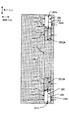
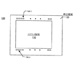
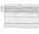
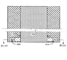
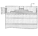
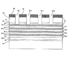
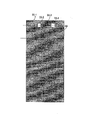
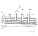
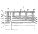
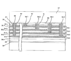
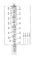
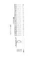
図1は、3次元構造を含んだデバイスの断面図を示しており、該3次元構造は、デバイス内の様々なレベル(階層)160−1乃至160−4まで導電体180が延在した小さいフットプリント(設置面積)の相互接続構造190を有する。図示した例においては、4つのレベル160−1乃至160−4が示されている。より一般的には、ここで説明する小型相互接続構造190は、Nは少なくとも2として、レベル0乃至Nを有する構造で実現されることができる。
FIG. 1 shows a cross-sectional view of a device including a three-dimensional structure, which is a
導電体180は、相互接続構造190内で、様々なレベル160−1乃至160−4のランドエリアに接触するように配設されている。より詳細に後述するように、各特定レベルの導電体180は、上に位置するレベル内の開口中を延在して、ランドエリア161−1a、161−1b、161−2a、161−2b、161−3a、161−3b、161−4に接触している。導電体180は、この例において、コンタクトレベル160−1乃至160−4を、レベル160−1乃至160−4の上に位置する配線層の相互接続ライン185に結合させるために使用されている。
The
ランドエリアは、導電体180との接触のために使用されるコンタクトレベル160−1乃至160−4の部分である。ランドエリアのサイズは、導電体180が様々なコンタクトレベル160−1乃至160−4のランドエリア内で導電性ランドエリアを上に位置する相互接続ライン185に適切に結合するための場所を提供するように、且つ、例えば様々なレベルのランドエリアに関して導電体180と上に位置するレベル内の開口との間でのミスアライメントなどの問題を解決するように、十分な大きさにされる。
The land area is a part of contact levels 160-1 to 160-4 used for contact with the
ランドエリアのサイズは、故に、使用される導電体のサイズ及び個数を含む多数の要因に依存し、実施形態ごとに異なったものとなる。また、導電体180の数は、ランドエリアごとに異なっていてもよい。
The size of the land area thus depends on a number of factors including the size and number of conductors used and will vary from embodiment to embodiment. Further, the number of
図示した例において、レベル160−1乃至160−4は、例えばドープトポリシリコンなどの材料のそれぞれの平面状導電層で構成され、絶縁材料の層165がレベル160−1乃至160−4を分離している。他の例では、レベル160−1乃至160−4は平面状の積層材料層である必要はなく、それに代えて、材料層は縦方向寸法において変化してもよい。
In the illustrated example, levels 160-1 through 160-4 are comprised of respective planar conductive layers of material such as doped polysilicon, for example, and an insulating
異なるレベル160−1乃至160−4に接触する複数の導電体180は、図1に示した断面に沿う方向に配列されている。この、異なるレベル160−1乃至160−4に接触する複数の導電体180の配列によって定められる方向を、ここでは、“長さ”方向と呼ぶ。“横断”方向は、長さ方向に垂直であり、図1に示した断面図に出入りする方向である。長さ方向及び横断方向は何れも、レベル160−1乃至160−4の平面図の2次元エリア内にある方向を意味し、“横方向の次元”であると見なされる。構造又は造形部の“長さ”は長さ方向におけるその長さであり、その“幅”は横断方向におけるその幅である。
The plurality of
レベル160−1は、複数のレベル160−1乃至160−4のうちの最も下のレベルである。レベル160−1は絶縁層164上にある。
The level 160-1 is the lowest level among the plurality of levels 160-1 to 160-4. Level 160-1 is on the insulating
レベル160−1は、導電体180との接触のための第1及び第2のランドエリア161−1a、161−1bを含んでいる。
The level 160-1 includes first and second land areas 161-1a and 161-1b for contact with the
図1において、レベル160−1は、2つのランドエリア161−1a、161−1bを、相互接続構造190の反対側の端部に含んでいる。一部の代替実施形態において、ランドエリア161−1a、161−1bのうちの一方は省略される。
In FIG. 1, level 160-1 includes two land areas 161-1a, 161-1b at the opposite end of the
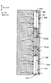
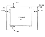
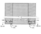
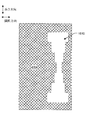
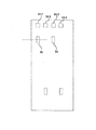
図2Aは、相互接続構造190のフットプリント内の、ランドエリア161−1a、161−1bを含むレベル160−1の部分の平面図である。相互接続構造190のフットプリントは、導電体のビアサイズの幅に近い幅とすることができ、且つ該幅より遙かに長いものとし得る長さを有することができる。図2Aに示すように、ランドエリア161−1aは、横断方向に幅200を有し、長さ方向に長さ201を有する。ランドエリア161−1bは、横断方向に幅202を有し、長さ方向に長さ203を有する。図2Aの実施形態において、ランドエリア161−1a、161−1bは各々、長方形の横断面を有している。実施形態において、ランドエリア161−1a、161−1bは各々、円形、楕円形、正方形、長方形、又は幾らか不規則な形状を有していてもよい。
FIG. 2A is a plan view of the portion of level 160-1 that includes land areas 161-1a, 161-1b within the footprint of
レベル160−1は最も下のレベルであるため、導電体180は、レベル160−1を貫通して下地の層に達する必要はない。故に、この例において、レベル160−1は相互接続構造190内に開口を有していない。
Since level 160-1 is the lowest level,
再び図1を参照するに、レベル160−2はレベル160−1の上に位置する。レベル160−2は、レベル160−1のランドエリア161−1aの上に位置する開口250を含んでいる。開口250は、開口250の長さ252を定める長さ方向の遠位の側壁251aと長さ方向の近位の側壁252とを有する。開口250の長さ252は少なくとも、下に位置するランドエリア161−1aの長さ201と同じ大きさであり、その結果、ランドエリア161−1aのための導電体180はレベル160−2を通過することができる。
Referring again to FIG. 1, level 160-2 is located above level 160-1. Level 160-2 includes an
レベル160−2はまた、ランドエリア161−1bの上に位置する開口255を含んでいる。開口255は、開口255の長さ257を定める長さ方向の遠位及び近位の側壁256a、256bを有する。開口255の長さ257は少なくとも、下に位置するランドエリア161−1bの長さ203と同じ大きさであり、その結果、ランドエリア161−1bのための導電体180はレベル160−2を通過することができる。
Level 160-2 also includes an
レベル160−2はまた、開口250、255と隣接して、それぞれ、第1及び第2のランドエリア161−2a、161−2bを含んでいる。第1及び第2のランドエリア161−2a、161−2bは、導電体180との接触のために使用されるレベル160−2の部分である。
Level 160-2 also includes first and second land areas 161-2a, 161-2b, adjacent to
図2Bは、相互接続構造190内の、第1及び第2のランドエリア161−2a、161−2b並びに開口250、255を含むレベル160−2の部分の平面図である。
FIG. 2B is a plan view of the portion of level 160-2 that includes first and second land areas 161-2a, 161-2b and
図2Bに示すように、開口250は、長さ252を定める長さ方向の側壁251a、251bを有するとともに、開口250の幅254を定める横断方向の側壁253a、253bを有する。幅254は少なくとも、下に位置するランドエリア161−1aの幅200と同じ大きさであり、その結果、導電体180は開口250を通過することができる。
As shown in FIG. 2B, the
開口255は、長さ257を定める長さ方向の側壁256a、256bを有するとともに、幅259を定める横断方向の側壁258a、258bを有する。幅259は少なくとも、下に位置するランドエリア161−1bの幅202と同じ大きさであり、その結果、導電体180は開口255を通過することができる。
図2Bの平面図において、開口250、255は各々、長方形の横断面を有している。実施形態において、開口250、255は各々、それらを形成するために使用されるマスクの形状に応じて、円形、楕円形、正方形、長方形、又は幾らか不規則な形状の横断面を有していてもよい。
In the plan view of FIG. 2B, the
図2Bに示すように、ランドエリア161−2aは開口250に隣接するとともに、横断方向の幅204と長さ方向の長さ205とを有する。ランドエリア161−2bは開口255に隣接するとともに、横断方向の幅206と長さ方向の長さ207とを有する。
As shown in FIG. 2B, the land area 161-2a is adjacent to the
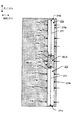
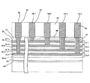
再び図1を参照するに、レベル160−3はレベル160−2の上に位置する。レベル160−3は、レベル160−1のランドエリア161−1a及びレベル160−2のランドエリア161−2aの上に位置する開口260を含んでいる。開口260は、開口260の長さ262を定める長さ方向の遠位及び近位の側壁261a、261bを有する。開口260の長さ262は少なくとも、下に位置するランドエリア161−1a及び161−2aの長さ201及び205の和と同じ大きさであり、その結果、ランドエリア161−1a及び161−2aのための導電体180はレベル160−3を通過することができる。
Referring again to FIG. 1, level 160-3 is located above level 160-2. Level 160-3 includes an
図1にて見て取れるように、開口260の長さ方向の遠位の側壁261aは、下に位置する開口250の長さ方向の遠位の側壁251aと縦方向に整列される。より詳細に後述する実施形態の製造において、これらの開口は、単一のエッチングマスクの開口及び該単一のエッチングマスクの開口上に形成される1つの追加マスクと、クリティカルなアライメント工程なしで該追加マスクをエッチングするプロセスとを用いて形成されることができ、該単一のエッチングマスクの周縁に沿って縦方向に整列された長さ方向の遠位側壁(261a、251a、・・・)を有する開口群の形成がもたらされる。
As can be seen in FIG. 1, the longitudinal
レベル160−3はまた、レベル160−1のランドエリア161−1b及びレベル160−2のランドエリア161−2bの上に位置する開口265を含んでいる。開口265は、開口265の長さ267を定める長さ方向の外側及び内側の側壁266a、266bを有する。開口265の長さ方向の外側の側壁266aは、下に位置する開口255の長さ方向の外側の側壁256aと縦方向に整列される。
Level 160-3 also includes an
開口265の長さ267は少なくとも、下に位置するランドエリア161−1b及び161−2bの長さ203及び207の和と同じ大きさであり、その結果、ランドエリア161−1b及び161−2bのための導電体180はレベル160−3を通過することができる。
The
レベル160−3はまた、開口260、265と隣接して、それぞれ、第1及び第2のランドエリア161−3a、161−3bを含んでいる。第1及び第2のランドエリア161−3a、161−3bは、導電体180との接触のために使用されるレベル160−3の部分である。
Level 160-3 also includes first and second land areas 161-3a, 161-3b, adjacent to
図2Cは、相互接続構造190内の、第1及び第2のランドエリア161−3a、161−3b並びに開口260、265を含むレベル160−3の部分の平面図である。
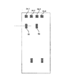
FIG. 2C is a plan view of the portion of level 160-3 that includes first and second land areas 161-3a, 161-3b and
図2Cに示すように、開口260は、長さ262を定める長さ方向の外側及び内側の側壁261a、261bを有するとともに、開口260の幅264a、264bを定める横断方向の側壁263a、263bを有する。幅264aは少なくとも、下に位置するランドエリア161−1aの幅200と同じ大きさであり、幅264bは少なくとも、下に位置するランドエリア161−2aの幅204と同じ大きさであり、その結果、導電体180は開口260を通過することができる。
As shown in FIG. 2C, the
図示した実施形態において、幅264a及び264bは実質的に同一である。他の例では、幅264a及び264bは、異なる幅を有するランドエリアに適合するように異なっていてもよい。
In the illustrated embodiment, the
開口265は、長さ267を定める長さ方向の側壁266a、266bを有するとともに、幅269a、269bを定める横断方向の側壁268a、268bを有する。幅269aは少なくとも、下に位置するランドエリア161−1bの幅202と同じ大きさであり、幅269bは少なくとも、下に位置するランドエリア161−2bの幅206と同じ大きさであり、その結果、導電体180は開口265を通過することができる。
図2Cに示すように、ランドエリア161−3aは開口260に隣接するとともに、横断方向の幅214と長さ方向の長さ215とを有する。ランドエリア161−3bは開口265に隣接するとともに、横断方向の幅216と長さ方向の長さ217とを有する。
As shown in FIG. 2C, the land area 161-3 a is adjacent to the
再び図1を参照するに、レベル160−4はレベル160−3の上に位置する。レベル160−4は、レベル160−1のランドエリア161−1a、レベル160−2のランドエリア161−2a及びレベル160−3のランドエリア161−3aの上に位置する開口270を含んでいる。開口270は、開口270の長さ272を定める長さ方向の側壁271a、271bを有する。開口270の長さ272は少なくとも、下に位置するランドエリア161−1a、161−2a及び161−3aの長さ201、205及び215の和と同じ大きさであり、その結果、ランドエリア161−1a、161−2a及び161−3aのための導電体180はレベル160−4を通過することができる。図1に示すように、開口270の長さ方向の側壁271aは、下に位置する開口260の長さ方向の側壁261aと縦方向に整列される。
Referring back to FIG. 1, level 160-4 is above level 160-3. Level 160-4 includes an
レベル160−4はまた、レベル160−1のランドエリア161−1b、レベル160−2のランドエリア161−2b及びレベル160−3のランドエリア161−3bの上に位置する開口275を含んでいる。開口275は、開口275の長さ277を定める長さ方向の側壁276a、276bを有する。開口275の長さ方向の側壁276aは、下に位置する開口265の長さ方向の側壁266aと縦方向に整列される。
Level 160-4 also includes an
開口275の長さ277は少なくとも、下に位置するランドエリア161−1b、161−2b及び161−3bの長さ203、207及び217の和と同じ大きさであり、その結果、ランドエリア161−1b、161−2b及び161−3bのための導電体180はレベル160−4を通過することができる。
The
レベル160−4はまた、開口270と275との間にランドエリア161−4を含んでいる。ランドエリア161−4は、導電体180との接触のために使用されるレベル160−4の部分である。図1において、レベル160−4は1つのランドエリア161−4を有している。他の例では、レベル160−4は2つ以上のランドエリアを含んでいてもよい。
Level 160-4 also includes a land area 161-4 between
図2Dは、相互接続構造190内の、ランドエリア161−4及び開口270、275を含むレベル160−4の部分の平面図である。
FIG. 2D is a plan view of the portion of level 160-4 that includes land area 161-4 and
図2Dに示すように、開口270は、長さ272を定める長さ方向の側壁271a、271bを有するとともに、開口270の幅274a、274b、274cを定める横断方向の側壁273a、273bを有する。幅274a、274b、274cは少なくとも、下に位置するランドエリア161−1a、161−2a、161−3aの幅200、204、214と同じ大きさであり、その結果、導電体180は開口270を通過することができる。
As shown in FIG. 2D, the
開口275は、長さ277を定める長さ方向の側壁276a、276bを有するとともに、幅279a、279b、279cを定める横断方向の側壁278a、278bを有する。幅279a、279b、279cは少なくとも、下に位置するランドエリア161−1b、161−2b、161−3bの幅202、206、216と同じ大きさであり、その結果、導電体180は開口275を通過することができる。
図2Dに示すように、ランドエリア161−4は開口270と275との間にあり、横断方向の幅224と長さ方向の長さ225とを有する。
As shown in FIG. 2D, land area 161-4 is between
再び図1を参照するに、開口270、260及び250の長さ方向の遠位側壁271a、261a及び251aは縦方向にアライメントされており、故に、開口270、260及び250の長さの差は側壁271b、261b及び251bの横方向のオフセットによるものである。ここで使用される要素又は造形部が“縦方向にアライメントされる”は、横断方向及び長さ方向の双方に垂直な仮想平面と実質的に同一平面にあることを表す。ここでは、“実質的に同一平面にある”なる用語は、単一のエッチングマスク内の開口と側壁の平面性にバラつきを生じさせ得る複数のエッチングプロセスとを使用する開口の形成における製造公差を受け入れることを意図して使用される。
Referring again to FIG. 1, the longitudinal
図1に示すように、開口275、265及び255の長さ方向の側壁276a、266a及び256aも縦方向にアライメントされている。
As shown in FIG. 1, the
同様に、これらのレベルの開口の横断方向の側壁も縦方向にアライメントされる。図2A−2Dを参照するに、開口270、260及び250の横断方向の側壁273a、263a及び253aは縦方向にアライメントされる。さらに、横断方向の側壁273b、263b及び253bは縦方向にアライメントされる。開口275、265及び255では、長さ方向の側壁276a、276a及び256aが縦方向にアライメントされ、横断方向の側壁278b、268b及び258bは縦方向にアライメントされる。
Similarly, the transverse sidewalls of these levels of openings are also vertically aligned. Referring to FIGS. 2A-2D, the transverse sidewalls 273a, 263a and 253a of the
図示した実施形態において、様々なレベル160−1乃至160−4の開口は、横断方向において実質的に同じ幅を有している。他の例では、これらの開口の幅は、異なる幅を有するランドエリア群に適合するように、例えばステップ状など、長さ方向に沿って変化することができる。 In the illustrated embodiment, the openings of the various levels 160-1 through 160-4 have substantially the same width in the transverse direction. In other examples, the widths of these openings can vary along the length direction, eg, stepped, to accommodate land areas having different widths.
ここで説明する相互接続構造190のこの実装技術は、従来技術と比較して、複数のレベル160−1乃至160−4へのコンタクトを製造するのに必要な面積又はフットプリントを有意に削減する。結果として、より多くの空間が、様々なレベル160−1乃至160−4にメモリ回路を実装するために利用可能になる。これは、従来技術と比較して、上側のレベル群におけるより高いメモリ密度とより低いビット当たりコストとを可能にする。
This implementation of the
図1の断面図において、相互接続構造190内の開口は、レベル160−4のランドエリア161−4の両側に階段状パターンを有するレベル群を生じさせる。すなわち、各レベルの2つの開口は、長さ方向及び横断方向の双方に垂直な軸を中心にして対称であり、各レベルの2つのランドエリアも該軸を中心にして対称である。ここでは、“対称”なる用語は、単一のエッチングマスク内の開口と開口の寸法にバラつきを生じさせ得る複数のエッチングプロセスとを使用する開口の形成における製造公差を受け入れることを意図して使用される。
In the cross-sectional view of FIG. 1, the openings in the
各レベルが単一の開口と単一のランドエリアとを含む代替的な実施形態においては、レベル群は一方側にのみ階段状パターンを有する。 In an alternative embodiment where each level includes a single opening and a single land area, the level group has a stepped pattern on only one side.
図示した例においては、4つのレベル160−1乃至160−4が示されている。より一般的には、ここで説明する小型相互接続構造は、Nは少なくとも2として、レベル0乃至N内に実装されることができる。一般に、(i)は1乃至Nに等しいとして、レベル(i)はレベル(i−1)の上にあり、レベル(i)のランドエリア(i)に隣接した開口(i)を有する。開口(i)はレベル(i−1)のランドエリア(i−1)上に延在し、また、iが2以上では、レベル(i−1)の隣接する開口(i−1)上に延在する。開口(i)は、レベル(i−1)内の開口(i−1)の長さ方向の遠位側壁にアライメントされた長さ方向の遠位側壁と、開口(i)の長さを定める長さ方向の近位側壁とを有する。開口(i)の長さは少なくとも、存在する場合には開口(i−1)の長さを足し合わせた、ランドエリア(i−1)の長さと同じ大きさである。(i)が2以上の場合、開口(i)は、レベル(i−1)内の開口(i−1)の横断方向の側壁とアライメントされた横断方向の側壁を有し、ランドエリア(i−1)の幅と同じ大きさ以上の開口(i)の幅を画成する。
In the illustrated example, four levels 160-1 to 160-4 are shown. More generally, the small interconnect structure described herein can be implemented in
代替的な実施形態において、その他の種類のメモリセル及び構成も使用され得る。使用され得るその他の種類のメモリセルの例には、誘電体電荷トラップ・フローティングゲートメモリセルが含まれる。例えば、一代替例において、デバイスのレベル群は、薄膜トランジスタ又は関連技術を用いてアクセスデバイス及びアクセスライン(配線)が当該レベル群内に形成された、絶縁材料によって分離された複数の平面状メモリセルアレイとして実装されてもよい。また、ここで説明する相互接続構造は、デバイスの様々なレベルに延在する導電体を小さいフットプリント内に有することが有用なその他の種類の3次元積層集積回路デバイス内に実装されることができる。 In alternative embodiments, other types of memory cells and configurations can be used. Examples of other types of memory cells that can be used include dielectric charge trapping floating gate memory cells. For example, in one alternative, a level group of devices comprises a plurality of planar memory cell arrays separated by an insulating material in which access devices and access lines (wirings) are formed in the level group using thin film transistors or related technology. May be implemented as Also, the interconnect structures described herein may be implemented in other types of three-dimensional stacked integrated circuit devices where it is useful to have conductors that extend to various levels of the device in a small footprint. it can.
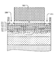
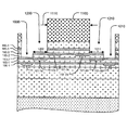
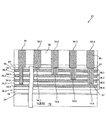
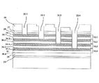
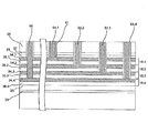
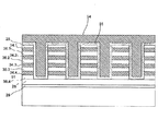
図3Aは、メモリアレイ領域110とここで説明する相互接続構造190を有する周辺領域120とを含んだ3次元積層集積回路デバイス100の一部を示す断面図である。
FIG. 3A is a cross-sectional view illustrating a portion of a three-dimensional stacked
図3Aにおいて、メモリアレイ領域110は、本願の譲受人によって所有されるLungによる米国特許出願第12/430290号に記載されるようなワンタイムプログラマブル・マルチレベルメモリセルとして実装されている。なお、該米国特許出願の内容をここに援用する。ここでは、それを、ここで説明する3D相互接続構造を実装可能な代表的な集積回路構造として説明する。
In FIG. 3A,
メモリアレイ領域110は、横型電界効果トランジスタアクセスデバイス131a、131bを含んだメモリアクセス層112を含んでいる。デバイス131a、131bは、半導体基板130内にソース領域132a、132b及びドレイン領域134a、134bを有している。基板130は、バルクシリコン、絶縁層上のシリコン層、又は集積回路を支持するための技術的に知られたその他の構造を有し得る。トレンチアイソレーション構造135a、135bが基板130内の領域群を分離している。ワードライン140a、140bがアクセスデバイス131a、131bのゲートとして機能する。コンタクトプラグ142a、142bが層間誘電体144を貫いて延在して、ドレイン領域134a、134bをビットライン150a、150bに結合している。
The
コンタクトパッド152a、152bが、下に位置するコンタクト146a、146bに結合され、アクセストランジスタのソース領域132a、132bへの接続を提供している。コンタクトパッド152a、152b及びビットライン150a、150bは層間誘電体154内にある。
図示した例において、レベルは、例えばドープトポリシリコンなどの材料のそれぞれの平面状導電層で構成される。他の例では、レベルは平面状の積層材料層である必要はなく、それに代えて、材料層は縦方向寸法において変化してもよい。 In the illustrated example, the level is comprised of a respective planar conductive layer of material such as doped polysilicon. In other examples, the level need not be a planar laminated material layer; instead, the material layer may vary in the longitudinal dimension.
絶縁層165−1乃至165−3がレベル160−1乃至160−4を互いに分離している。絶縁層166がレベル160−1乃至160−4及び絶縁層165−1乃至165−3の上に位置している。
Insulating layers 165-1 through 165-3 separate levels 160-1 through 160-4 from one another. Insulating
複数の電極ピラー171a、171bが、メモリセルアクセス層112の頂部に配置され、レベル群を貫いて延在している。この図において、第1の電極ピラー171aは、例えばタングステン又はその他の好適電極材料からなる中心の導電性コア170aを含んでおり、導電性コア170aはポリシリコンのシース(覆い)172aによって囲まれている。アンチヒューズ材料又はその他のプログラム可能メモリ材料の層174aが、ポリシリコンシース172aと複数のレベル160−1乃至160−4との間に形成されている。この例において、レベル160−1乃至160−4は比較的高濃度にドープされたn型ポリシリコンを有し、ポリシリコンシース172aは比較的低濃度にドープされたp型ポリシリコンを有する。好ましくは、ポリシリコンシース172aの厚さは、p−n接合によって形成される空乏領域の深さより大きくされる。空乏領域の深さは、部分的に、p−n接合を形成するために使用されるn型及びp型のポリシリコンの相対的なドーピング濃度によって決定される。レベル160−1乃至160−4及びポリシリコンシース172aはまた、アモルファスシリコンを用いて実装されてもよい。また、その他の半導体材料も使用され得る。
A plurality of
第1の電極ピラー171aはパッド152aに結合されている。導電性コア170b、ポリシリコンシース172b及びアンチヒューズ材料層174bを含んだ第2の電極ピラー171bは、パッド152bに結合されている。
The
複数のレベル160−1乃至160−4とピラー171a、171bとの間の界面領域は、より詳細に後述するように、整流器と直列にされたプログラム可能素子を有するメモリ素子を含んでいる。
The interface region between the plurality of levels 160-1 through 160-4 and the
ピラー171aのアンチヒューズ材料の層174aは、二酸化シリコン、酸窒化シリコン又はその他のシリコン酸化物とすることができ、生来状態において高い抵抗を有する。例えば窒化シリコンなどのその他のアンチヒューズ材料が使用されてもよい。ワードライン140、ビットライン150及び複数のレベル160−1乃至160−4に適切な電圧を印加することによってプログラムした後、アンチヒューズ材料層174aは絶縁破壊し、対応するレベルに隣接するアンチヒューズ材料内のアクティブ領域が低い抵抗状態を担う。
The
図3Aに示すように、レベル160−1乃至160−4の複数の導電層は周辺領域120内まで延在しており、そこには、複数のレベル160−1乃至160−4に対して支援回路及び導電体180が製造されている。周辺領域120には多様なデバイスが実装されて、集積回路100上の復号化ロジック及びその他の回路を支援する。
As shown in FIG. 3A, the plurality of conductive layers at levels 160-1 through 160-4 extend into the
導電体180は相互接続構造190内に配置され、様々なレベル160−1乃至160−4のランドエリアに接触している。より詳細に後述するように、各特定レベル160−1乃至160−4への導電体180は、上に位置するレベル内の開口を通って、導電性の相互接続配線185を含む配線層まで延在している。相互接続配線185は、レベル160−1乃至160−4と周辺120内の復号回路との間の相互接続を提供する。
The
図3Aの破線によって表されるように、相異なるレベル160−1乃至160−4に接触する複数の導電体180が、図3Aに示した断面に出入りする方向である長さ方向に配列されている。
As represented by the broken lines in FIG. 3A, a plurality of
図3Bは、図3Aの相互接続構造190を通る直線Fig.3B−Fig.3Bに沿って取られた長さ方向の断面図であり、図1に示したものと同様の相互接続構造190の様子を示している。図3Bにて見て取れるように、各特定のレベルのための導電体180は、上に位置するレベル内の開口を通って延在して、ランドエリアに接触している。
3B shows a straight line FIG. 3 through the
図示した例においては、4つのレベル160−1乃至160−4が示されている。より一般的には、ここで説明する小型相互接続構造は、Nは少なくとも2として、レベル0乃至N内に実装されることができる。
In the illustrated example, four levels 160-1 to 160-4 are shown. More generally, the small interconnect structure described herein can be implemented in
代替的な実施形態において、その他の種類のメモリセル及び構成も使用され得る。例えば、一代替例において、デバイスのレベル群は、薄膜トランジスタ又は関連技術を用いてアクセスデバイス及びアクセスラインが当該レベル群内に形成された、絶縁材料によって分離された複数の平面状メモリセルアレイとして実装されてもよい。また、ここで説明する相互接続構造は、デバイスの様々なレベルに延在する導電体を小さいフットプリント内に有することが有用なその他の種類の3次元積層集積回路デバイス内に実装されることができる。 In alternative embodiments, other types of memory cells and configurations can be used. For example, in one alternative, a level group of devices is implemented as a plurality of planar memory cell arrays separated by an insulating material in which access devices and access lines are formed in the level group using thin film transistors or related technology. May be. Also, the interconnect structures described herein may be implemented in other types of three-dimensional stacked integrated circuit devices where it is useful to have conductors that extend to various levels of the device in a small footprint. it can.
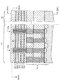
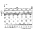
図3A−3Bにおいては、単一の相互接続構造190が示されている。より均一な電力分布を実現するように、例えばメモリアレイ領域110を取り囲んでなど、デバイス内の様々な位置に複数の相互接続構造が配設されてもよい。図4は、アレイのそれぞれの側の周辺部120内の領域のシリーズ190−1及び190−2を含む2組の一連の相互接続構造を含んだデバイス100の一実施形態の上面レイアウト図を示している。図5は、アレイの4辺全ての周辺部120内のシリーズ190−1、190−2、190−3及び190−4を含む4組の一連の相互接続構造を含んだ一実施形態の上面レイアウト図を示している。1000列×1000行のセルを含む一例に係るアレイサイズにおいて、10レベルを有し、形状サイズFがワードライン幅及びビットライン幅を規定し、レベル群のランドエリアのサイズがおよそFである場合、1つの相互接続構造によって占有される領域の長さはレベル数のおよそ2F倍すなわち20Fであり、ワードラインごとのピッチはおよそ2F以上であり、アレイの幅がおよそ2000Fとなることがわかる。故に、この例によれば、およそ100個の相互接続構造を、アレイ幅に沿った例えばシリーズ190−3などのシリーズにして形成することができ、同様の数をアレイ長さに沿って例えばシリーズ190−1などのシリーズにして形成することができる。
In FIGS. 3A-3B, a
更なる他の代替実施形態において、周辺部120内に相互接続構造を有することに加えて、あるいは代えて、1つ以上の相互接続構造をメモリアレイ領域110内に実装することができる。また、相互接続構造は、メモリアレイ領域110の辺に平行ではなく、対角線方向又は何らかのその他の方向に延在されてもよい。
In still other alternative embodiments, one or more interconnect structures can be implemented in the
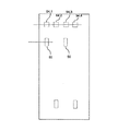
図6は、ここで説明する相互接続構造を含むメモリデバイスの一部を示す模式図である。第1の電極ピラー171aが、ビットライン150a及びワードライン140aを用いて選択されるアクセストランジスタ131aに結合されている。ピラー171aには複数のメモリ素子544−1乃至544−4が接続されている。各メモリ素子は、整流器549に直列のプログラム可能素子548を含んでいる。この直列構成は、アンチヒューズ材料の層がp−n接合の位置に置かれてはいるが、図3A−3Bに示した構造を表している。プログラム可能素子548は、アンチヒューズを指し示すためにしばしば使用される記号によって表されている。しかしながら、理解されるように、その他の種類のプログラム可能な抵抗材料及び構造も使用され得る。
FIG. 6 is a schematic diagram illustrating a portion of a memory device including an interconnect structure described herein. The
また、導電面と電極ピラー内のポリシリコンとの間のp−n接合によって実現される整流器549は、その他の整流器によって置き換えられることが可能である。例えば、整流器を提供するため、ゲルマニウムシリサイドのような固体電解質又はその他の好適材料に基づく整流器が使用され得る。その他の代表的な固体電解質材料については米国特許第7382647を参照することができる。
Also, the
メモリ素子544−1乃至544−4の各々は、対応する導電性レベル160−1乃至160−4に結合されている。レベル160−1乃至160−4は導電体180及び相互接続配線185を介してプレイン(plane)デコーダ546に結合されている。プレインデコーダ546は、アドレスに応答して、選択されたレベルに、メモリ素子内の整流器が順バイアスされて導通するように例えばグランド547などの電圧を印加するとともに、選択されていないレベルに、メモリ素子内の整流器が逆バイアスされる、あるいは非導通となるように電圧を印加するかフローティングにするかする。
Each of memory elements 544-1 through 544-4 is coupled to a corresponding conductivity level 160-1 through 160-4. Levels 160-1 through 160-4 are coupled to a
図7は、ここで説明する相互接続構造を有する3Dメモリアレイ360を含む集積回路デバイス300の簡略化したブロック図である。ローデコーダ361が、メモリアレイ360のロー(行)群に沿って配列された複数のワードライン140に結合されている。コラムデコーダ363が、アレイ360内のメモリセルに対するデータの読み出し及びプログラミングを行うために、メモリアレイ360のコラム(列)群に沿って配列された複数のビットライン150に結合されている。プレインデコーダ546が、導電体180及び相互接続配線185を介して、メモリアレイ360内の複数のレベル160−1乃至160−4に結合されている。バス365上で、アドレスがローデコーダ361、コラムデコーダ363及びプレインデコーダ546に供給される。この例において、ブロック366内のセンス増幅器及びデータイン(data-in)構造が、データバス367を介してコラムデコーダ363に結合されている。データは、集積回路300の入力/出力ポートからブロック366内のデータイン構造へ、データインライン371を介して供給される。図示した実施形態において、集積回路300には、例えば、汎用プロセッサ若しくは専用アプリケーション回路、又はシステム・オン・チップ機能を提供する複数のモジュールの組み合わせなどの、その他回路374が含まれている。データは、ブロック366のセンス増幅器から、集積回路300の入力/出力ポートへ、あるいは集積回路の内部又は外部のその他のデータ宛先へ、データアウトライン372を介して供給される。この例ではバイアス構成状態機械369を用いて実装されているコントローラが、ブロック368内の1つ又は複数の電源によって生成あるいは提供されるバイアス構成供給電圧、例えば読み出し電圧及びプログラム電圧など、の印加を制御する。コントローラは、技術的に知られた専用論理回路を用いて実装され得る。他の実施形態において、コントローラは、同一の集積回路上に実装され得る汎用プロセッサを有し、それがコンピュータプログラムを実行してデバイスの動作を制御する。更なる他の実施形態においては、コントローラの実装のために、専用論理回路と汎用プロセッサとの組み合わせが用いられてもよい。
FIG. 7 is a simplified block diagram of an
図8A−8C乃至図15は、ここで説明する非常に小さいフットプリントを有する相互接続構造を製造するための製造シーケンスの一実施形態における工程群を示している。 FIGS. 8A-8C through 15 illustrate the steps in one embodiment of a manufacturing sequence for manufacturing an interconnect structure having a very small footprint as described herein.
図8A及びCは、製造シーケンスの第1の工程の断面図を示しており、図8Bはその上面図を示している。この用途の目的のため、第1の工程は、配設されたメモリセルアクセス層112の上に複数のレベル160−1乃至160−4を形成することを含む。図示した実施形態において、図8A−8Cに示した構造は、本願の譲受人によって共通に所有されるLungによる米国特許出願第12/430290号に記載されたプロセスを用いて形成される。なお、その内容をここに援用する。
8A and 8C show a cross-sectional view of the first step of the manufacturing sequence, and FIG. 8B shows a top view thereof. For purposes of this application, the first step includes forming a plurality of levels 160-1 through 160-4 on the disposed memory
他の実施形態において、レベル群は、技術的に知られた標準プロセスによって形成されることができ、ここで説明する相互接続構造が実装されるデバイスに応じて、例えばトランジスタ及びダイオード、ワードライン、ビットライン及びソースライン、導電性プラグ、並びに基板内のドープト領域など、アクセスデバイスを含んでいてもよい。 In other embodiments, the levels can be formed by standard processes known in the art, depending on the device in which the interconnect structure described herein is implemented, such as transistors and diodes, word lines, Access devices such as bit and source lines, conductive plugs, and doped regions in the substrate may also be included.
上述のように、他の実施形態において、その他の種類のメモリセル及びメモリアレイ領域110のその他の構成も用いられ得る。
As described above, other types of memory cells and other configurations of the
次に、図8A−8Cに示した構造上に、開口810を有する第1のマスク800が形成され、図9Aの上面図及び図9Bの断面図に示す構造が得られる。第1のマスク800は、第1のマスク800の層を堆積し、リソグラフィ技術を用いて、開口810を形成するように該層をパターニングすることによって形成され得る。第1のマスク800は例えば、窒化シリコン、酸化シリコン又は酸窒化シリコンなどのハードマスク材料を有し得る。
Next, a
第1のマスク800内の開口810は、レベル160−1乃至160−4のランドエリアの組み合わせの周囲を取り囲む。故に、開口810の幅192は、後に形成される導電体180がレベル160−1乃至160−4の開口を通過することができるよう、少なくとも、レベル160−1乃至160−4のランドエリアの幅と同じ大きさである。開口810の長さ194は、後に形成される導電体180がレベル160−1乃至160−4の開口を通過することができるよう、少なくとも、レベル160−1乃至160−4のランドエリアの長さの和と同じ大きさである。
Opening 810 in
次に、図9A−9Bに示した構造上に、開口810内を含めて、第2のエッチングマスク900が形成され、図10Aの上面図及び図10Bの断面図に示す構造が得られる。図示のように、第2のエッチングマスク900は、開口810の長さ194より小さい長さ910を有するとともに、開口810の幅192と少なくとも同じ大きさの幅を有する。
Next, a
図示した実施形態において、第2のエッチングマスク900は、開口810内の第2のマスク900の長さが後述の後続プロセス工程にて選択的に短縮されることができるよう、第1のマスク800に対して選択的にエッチングされることが可能な材料を有する。換言すれば、第2のマスク900の材料は、第2のマスク900の長さを短縮するために使用されるプロセスに関して、第1のマスク800の材料のエッチングレートより高いエッチングレートを有する。例えば、第1のマスク800がハードマスク材料を有する実施形態において、第2のマスクはフォトレジストを有することができる。
In the illustrated embodiment, the
次に、図10A−10Bに示した構造上で、第1及び第2のマスク800、900をエッチングマスクとして用いてエッチング処理が実行され、図11Aの上面図及び図11Bの断面図に示す構造が得られる。このエッチング処理は、例えばタイミングモードのエッチングを用いて、単一のエッチングケミストリを使用して実行され得る。他の例では、このエッチング処理は、絶縁層166、レベル160−4、絶縁材料165−3及びレベル160−3を個別にエッチングするように異なるエッチングケミストリを用いて実行され得る。
Next, an etching process is performed on the structure shown in FIGS. 10A and 10B using the first and
このエッチングは、レベル160−4を貫通してレベル160−3の一部を露出させる開口1000を形成する。開口1000は、レベル160−1のランドエリア161−1aの上に位置する。開口1000は、ランドエリア161−1aの長さと少なくとも同じ大きさの長さ1002を有するとともに、ランドエリア161−1aの幅と少なくとも同じ大きさの幅1004を有する。
This etching forms an
このエッチングはまた、レベル160−4を貫通してレベル160−3の一部を露出させる開口1010を形成する。開口1010は、レベル160−1のランドエリア161−1bの上に位置する。開口1010は、ランドエリア161−1bの長さと少なくとも同じ大きさの長さ1012を有するとともに、ランドエリア161−1bの幅と少なくとも同じ大きさの幅1004を有する。
This etch also forms an
次に、マスク900の長さ910が短縮されて、長さ1110を有する短縮長マスク1100が形成され、図12Aの上面図及び図12Bの断面図に示す構造が得られる。図示した実施形態において、マスク900はフォトレジストを有しており、例えばCl2ベースあるいはHBrベースのケミストリを用いた反応性イオンエッチングを用いて、トリミングされることができる。
Next, the
次に、図12A−12Bに示した構造上で、第1のマスク800及び短縮長マスク1100をエッチングマスクとして用いてエッチング処理が実行され、図13Aの上面図及び図13Bの断面図に示す構造が得られる。
Next, an etching process is performed on the structure shown in FIGS. 12A-12B using the
このエッチング処理は、レベル160−3を貫通して下に位置するレベル160−2の部分を露出させるように、開口1000、1010を延長させる。
This etching process extends the
このエッチングはまた、開口1200、1210を形成する。開口1200、1210は、マスク1100の長さの短縮によってもはやマスク1100に覆われなくなったレベル160−4の部分を貫通し、それによってレベル160−3の部分を露出させる。開口1200は、開口1000に隣接して形成され、且つレベル160−2のランドエリア161−2aの上に位置する。開口1200は、ランドエリア161−2aの長さと少なくとも同じ大きさの長さ1202を有するとともに、ランドエリア161−2aの幅と少なくとも同じ大きさの幅1204を有する。
This etch also forms
開口1210は、開口1010に隣接して形成され、且つレベル160−2のランドエリア161−2bの上に位置する。開口1210は、ランドエリア161−2bの長さと少なくとも同じ大きさの長さ1212を有するとともに、ランドエリア161−2bの幅と少なくとも同じ大きさの幅1204を有する。
次に、マスク1100の長さ1110が短縮されて、長さ1305を有する短縮長マスク1300が形成される。第1のマスク800及びマスク1300をエッチングマスクとして用いたエッチング処理が実行され、図14Aの上面図及び図14Bの断面図に示す構造が得られる。
Next, the
このエッチング処理は、レベル160−2を貫通してレベル160−1のランドエリア161−1a、161−1bを露出させるように、開口1000、1010を延長させる。このエッチング処理はまた、レベル160−3を貫通してレベル160−2のランドエリア161−2a、161−2bを露出させるように、開口1200、1210を延長させる。
This etching process extends the
このエッチングはまた、開口1310、1320を形成する。開口1310、1320は、マスク1300の長さの短縮によってもはや覆われなくなったレベル160−4の部分を貫通し、それによってレベル160−3のランドエリア161−3a、161−3bを露出させる。
This etch also forms
開口1310は、開口1200に隣接して形成される。開口1310は、ランドエリア161−3aの長さと少なくとも同じ大きさの長さ1312を有するとともに、ランドエリア161−3aの幅と少なくとも同じ大きさの幅1314を有する。
The
開口1320は、開口1210に隣接して形成される。開口1320は、ランドエリア161−3bの長さと少なくとも同じ大きさの長さ1322を有するとともに、ランドエリア161−3bの幅と少なくとも同じ大きさの幅1324を有する。
次に、図14A−14Bに示した構造上に絶縁充填材料1400が堆積され、且つ例えば化学機械研磨(CMP)などの平坦化プロセスが実行されてマスク800、1300が除去され、図15の断面図に示す構造が得られる。
Next, an insulating
次に、導電体180のためのランドエリアへのビアを画成するようにリソグラフィパターンが形成される。反応性イオンエッチングを適用して、絶縁充填材料1400を貫通する深い高アスペクト比のビアを形成することができ、それにより、導電体180用のビアが配設される。ビアを開口した後、ビアは、導電体180を形成するよう、タングステン又はその他の導電材料で充填される。その後、相互接続配線185を形成するようにメタライゼーションプロセスが適用され、導電体180とデバイスのプレインデコーダ回路との間の相互接続が提供される。最後に、バックエンドオブライン(BEOL)プロセスが適用されて集積回路が完成され、図3A−3Bに示した構造が得られる。
Next, a lithographic pattern is formed to define vias to land areas for the
下に位置するレベルのランドエリアまで導電体を通すために使用される様々なレベル内の開口群は、単一のエッチングマスク800内の開口810と、クリティカルなアライメント工程を用いない追加マスクをエッチングするプロセスとを用いて、それらレベル群をパターニングすることによって形成される。結果として、縦方向にアライメントされた側壁を有する様々なレベル内の開口群がセルフアライン的に形成される。
The openings in the various levels used to pass the conductor to the underlying level land area etch the
上述の例において、マスク800の開口810は、平面図において、長方形の断面を有する。その結果、様々なレベルの開口群は横断方向において実質的に同じ幅を有する。他の例では、マスク800の開口は、様々なレベルのランドエリアの形状に応じて、円形、楕円形、正方形、長方形、又は幾らか不規則な形状である断面を有していてもよい。
In the above example, the
例えば、マスク800の開口の幅は、異なる幅を有するランドエリア群に適合するように、長さ方向に沿って変化することができる。図16は、長さ方向においてステップ状に変化する幅を有するマスク800の開口1510の平面図を示している。開口1510は、それに従って、レベル群の開口群の幅を変化させる。
For example, the width of the opening of the
続いて、主として図17−34Aを参照して本発明を説明する。 Subsequently, the present invention will be described mainly with reference to FIGS. 17-34A.
以下の説明は典型的に、具体的な構造上の実施形態及び方法を参照してのものである。理解されるように、本発明は、具体的に開示される実施形態及び方法に限定されるものではなく、その他の特徴、要素、方法及び実施形態を用いて実施されてもよい。本発明を例示するために好適な実施形態を説明するが、本発明の範囲は、それらの実施形態によって限定されず、請求項によって定められる。当業者は、以下の説明を受けて、多様な均等な変形例を認識するであろう。様々な実施形態における同様の要素は、似通った参照符号をで用いて参照することとする。 The following description is typically with reference to specific structural embodiments and methods. As will be appreciated, the invention is not limited to the specifically disclosed embodiments and methods, but may be practiced with other features, elements, methods and embodiments. Preferred embodiments are described to illustrate the invention, but the scope of the invention is not limited by those embodiments, but is defined by the claims. Those of ordinary skill in the art will recognize a variety of equivalent variations upon receiving the following description. Similar elements in the various embodiments will be referred to with like reference numerals.
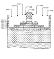
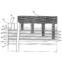
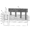
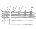
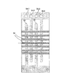
図17−34Aは、3次元積層ICデバイスの他の一例の構造及び製造方法を示しており、同様の構造物には似通った参照符号が付されている。図17及び17Aは、この例に係る3次元積層ICデバイスの相互接続領域17の簡略化した断面図及び平面図である。この例において、相互接続領域17は、18.1−18.4を付した4つの相互接続レベル18と、54.1−54.4を付した4つの導電体54と、グランド導電体55とを含んでいる。導電体54は、コンタクトレベル18の、34.1−34.4を付した導電層34の、14.1−14.4を付した相互接続コンタクト領域14のうちの1つに電気的に接続するために、コンタクトレベル18を通る第1の部分57と、層間誘電体52及び電荷トラップ層27を通る第2の部分59とを有している。第1の部分57は、誘電体の側壁スペーサ61によって囲まれており、それにより、導電体54は、その導電体が電気接触を形成しない導電層34から電気的に分離されている。また、各コンタクトレベル18の各導電層34に電気的に接続されたグランド導電体55が示されている。
FIGS. 17-34A show another example of the structure and manufacturing method of a three-dimensional stacked IC device, and similar structures are given similar reference numerals. 17 and 17A are a simplified cross-sectional view and plan view of the interconnect region 17 of the three-dimensional stacked IC device according to this example. In this example, interconnect region 17 includes four interconnect levels 18 labeled 18.1-18.4, four conductors 54 labeled 54.1-54.4, and
図18及び18Aは、相互接続領域17の製造における初期工程を示している。フォトレジスト88が、33.1−33.4を付したコンタクト開口33及び図18Aに示すグランドコンタクト開口35のエッチングに使用される。コンタクト開口33及びグランドコンタクト開口35は、上部層24を貫通し、第1のコンタクト層18.1の上側の導電層34.1を露出させる。コンタクト開口33のエッチングに続いて、フォトレジスト88が剥離され、図19及び19Aに示すように相互接続領域17上に第1のフォトレジストマスク89が形成される。第1のマスク89は1つおきにコンタクト開口を露出させ、すなわち、この例ではコンタクト開口33.2及び33.4を露出させる。図19Aにて見て取れるように、マスク89はまた、グランドコンタクト開口35を覆う。図17と図18とを比較することによって理解されるように、コンタクト開口33の位置は導電体54の位置を決定し、グランドコンタクト開口35の位置はグランド導電体55の位置を決定する。この例において、導電体54ひいては相互接続コンタクト領域14は一定のピッチを有する。
18 and 18A show the initial steps in the manufacture of the interconnect region 17.
図20及び20Aは、露出されたコンタクト開口33.2及び33.4の下の単一のコンタクトレベル18.1を貫通させるエッチングの結果を示している。その後、第1のマスク89は剥離され、続いて、図21及び21Aに示す第2のフォトレジストマスク90が形成される。第2のマスク90は、コンタクト開口33.1及び33.2並びにグランドコンタクト開口35を覆いながらコンタクト開口33.3及び33.4を露出させるために使用される。図21は、第1のマスク89の除去及び図20の構造上の第2のマスク90の形成の結果を示しており、左から数えて1番目及び2番目のコンタクト開口33.1及び33.2が第2のマスクで覆われ、3番目及び4番目のコンタクト開口33.3及び33.4が開放されている。
FIGS. 20 and 20A show the result of etching through a single contact level 18.1 under exposed contact openings 33.2 and 33.4. Thereafter, the
図22及び22Aは、3番目及び4番目のコンタクト開口33.3及び33.4の2つのコンタクトレベルを貫通させるエッチングの結果を示している。すなわち、コンタクト開口33.3を介してコンタクトレベル18.1及び18.2がエッチングされ、コンタクト開口33.4を介してコンタクトレベル18.2及び18.3がエッチングされる。図23及び23Aは、図22の第2のマスク90の除去後の図22の構造を示している。見て取れるように、コンタクト開口33.1−33.4は下方にコンタクトレベル18.1−18.4の導電層34.1−34.4まで延在している。
22 and 22A show the result of etching through the two contact levels of the third and fourth contact openings 33.3 and 33.4. That is, contact levels 18.1 and 18.2 are etched through contact opening 33.3, and contact levels 18.2 and 18.3 are etched through contact opening 33.4. 23 and 23A show the structure of FIG. 22 after removal of the
図24及び24Aは、コンタクト開口33.1−33.4の側壁への側壁スペーサ61の形成後の図23の構造を示している。側壁スペーサ61はコンタクト開口33.2、33.3及び33.4を、それらのコンタクト開口が通過するコンタクトレベル18の導電層34から電気的に絶縁する。
24 and 24A show the structure of FIG. 23 after formation of the
図25及び25Aは、図25にグランドコンタクト開口35を通る断面図を追加した図24の構造を示している。コンタクト開口33の全てがフォトレジスト92で覆われ、グランドコンタクト開口35は露出されたままにされている。図26及び26Aは、導電層34.1−34.4をグランドコンタクト開口35の内側に露出させる、グランドコンタクト開口35の位置の3つのコンタクトレベル18を貫通させるエッチングの後の、図25の構造を示している。図27及び27Aは、フォトレジスト92を除去した後の図26の構造を示している。
25 and 25A show the structure of FIG. 24 with the addition of a cross-sectional view through the
図28及び28Aは、典型的にはポリシリコンである導電材料93を堆積し、それにより、コンタクト開口33及びグランドコンタクト開口35を充填した後の、図27の構造を示している。コンタクト開口33及びグランドコンタクト開口35内の材料93は、それぞれ、導電体54及びグランド導電体55を形成する。所望の場合には、グランド導電体55とコンタクトレベル18の導電層34との間の電気接触を強化するため、グランドコンタクト開口35内にグランド導電体55を形成するのに先立って、グランドコンタクト開口の側壁の絶縁層36をエッチバックあるいはその他の方法で除去することができる。これは、図28に、グランド導電体55を囲む絶縁層36内の破線によって指し示されている。導電材料93はまた、上部層24の誘電体層26を覆っている。その後、図28の構造がエッチングされて、誘電体層26を覆う材料93の層が除去される。これは、図29及び29Aに示されている。図29の構造は電荷トラップ層27まで下方に、例えば化学機械研磨にかけられ、図30の構造が得られる。
FIGS. 28 and 28A illustrate the structure of FIG. 27 after depositing a
図31及び31Aは、典型的には窒化シリコンであるストッパ層96の堆積とそれに続くストッパ層上への層間誘電体97の堆積との後の図30の構造を示している。次に、図31の構造は、54.1−54.4を付した導電体54及びグランド導電体55まで層間誘電体97及びストッパ層96を貫通するように形成された、コンタクト開口33及びグランドコンタクト開口35の延在部を有するようにされる。これに続いて、図32及び32Aを参照するに、それら延在部への例えばタングステンなどの導電材料の充填が行われ、導電体54及びグランド導電体55が作り出される。導電体54は、コンタクトレベル18内を延在する第1の部分57と、上部層24内を延在する第2の部分59とを有する。
FIGS. 31 and 31A show the structure of FIG. 30 after deposition of a
一部の例において、層96は窒化シリコンであり、層間誘電体97は二酸化シリコンである。しかしながら、層96は、例えば二酸化シリコン又は酸化シリコンと窒化シリコンとの交互層など、その他の誘電体材料を有していてもよい。側壁スペーサ30は、窒化シリコンとし得るが、例えば二酸化シリコン又は多層の酸化物/窒化シリコンなど、その他の材料を有していてもよい。同様に、誘電体層25は、典型的には窒化シリコンであるが、例えば二酸化シリコンなどであってもよい。導電体54の第1の部分57は、典型的にはポリシリコンであるが、例えばN+ポリシリコン、タングステン、TiNなど、その他の導電材料であってもよい。また、導電体54の長さ全体が、例えばタングステンなどの同一材料であってもよい。
In some examples,
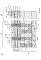
図33は、16個のコンタクト開口の組を図式的に示したものであり、4つの異なるセットのコンタクト開口33が、16個のコンタクトレベル18へのアクセスを提供するように、4つのマスクのみを用いて16個の異なる深さまでエッチングされることを示している。 FIG. 33 schematically shows a set of 16 contact openings, with only 4 masks so that 4 different sets of contact openings 33 provide access to 16 contact levels 18. It is shown that the etching is performed up to 16 different depths.
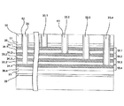
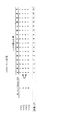
図34及び34Aは、3次元積層ICデバイスの断面図及び平面図である。図34は、1つのワードライン94を通るように取られており、ワードライン94は、層95によって、例えば誘電体層と半導体層とが交互にされたスタックから電気的に絶縁されている。層95は、例えば、酸化シリコンと、電荷トラップ層として機能する窒化シリコンとの交互層とし得る。
34 and 34A are a cross-sectional view and a plan view of a three-dimensional stacked IC device. FIG. 34 is taken through one
以下の例は、3次元積層ICデバイスの相互接続領域17のコンタクトレベル18のスタックにおいて、ランドエリア56への電気接続を実現する方法を説明するものである。この例において、相互接続領域17は上部層24と上部層の下のコンタクトレベル18のスタックとを含んでおり、各コンタクトレベルは導電層34と絶縁層36とを有する。相互接続領域17の上に位置する上部層24の少なくとも一部は、第1のコンタクトレベル18.1を露出させ且つ各コンタクトレベル18のコンタクト開口33を作り出すために除去される。これは図18に例示されている。
The following example describes a method for realizing electrical connection to the land area 56 in a stack at the contact level 18 in the interconnect region 17 of the three-dimensional stacked IC device. In this example, interconnect region 17 includes an
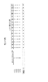
N個のエッチングマスクのセットを使用することで、コンタクトレベル18のスタックにおける相互接続コンタクト領域14の最大2N個のレベルが作り出される。殆どの図は4つのコンタクトレベル18を有する例を示していたが、この例においては、コンタクトレベルの数は16コンタクトレベル、故に、N=4まで増加される。ここでの説明においては、16個のコンタクト開口33の図形表示を含んだ図33も参照する。複数のマスクを用いて、最大2N個のコンタクトレベル、この例では16コンタクトレベル、のコンタクト開口33がエッチングされる。工程群は以下のように実行される。
Using a set of N etch masks creates up to 2 N levels of
第1のマスク89(図19参照)を用いて、1つおきのコンタクト開口にて、1つのコンタクトレベル18をエッチングする。第1のマスク89によって覆われないコンタクト開口は、図33において、コンタクト開口33.2、33.4などを囲む点線の枠によって識別されている。次に、第2のマスク90(図21参照)を用いて、一連の1番目乃至4番目のコンタクト開口の組における3番目及び4番目のコンタクト開口にて、2つのコンタクトレベルをエッチングする。第2のマスク90は、図33において、4個のコンタクト開口の組のうちの2つの隣接コンタクト開口を各枠が囲む4個の短破線の枠によって識別されている。この例において、エッチングされる3番目及び4番目のコンタクト開口は、第1のコンタクト開口33.1乃至第4のコンタクト開口33.4の組におけるコンタクト開口33.3及び33.4と、コンタクト開口33.5−33.8の組におけるコンタクト開口33.7及び33.8と、等々である。図22にて見て取れるように、第1及び第2のマスク89、90の使用により、4つのコンタクトレベル18.1−18.4の各々までのコンタクト開口33が提供される。
Using the first mask 89 (see FIG. 19), one contact level 18 is etched in every other contact opening. The contact opening not covered by the
16個のコンタクトレベル18を有するこの例を引き続き説明するに、第3のマスク(図示せず)を用いて、一連の1番目から8番目のコンタクト開口の組における5番目乃至8番目のコンタクト開口33にて、4つのコンタクトレベルをエッチングする。これは、図33に、2つの長破線の枠によって指し示されている。第4のマスク(図示せず)を用いて、一連の1番目乃至16番目のコンタクト開口の少なくとも1つの組における9番目乃至16番目のコンタクト開口にて、8つのコンタクトレベルをエッチングする。これは、図33に、1つの実線の枠によって指し示されている。なお、第1、第2、第3及び第4のマスクの各々を用いて、コンタクト開口群の半数がエッチングされる。 To continue this example with sixteen contact levels 18, a third mask (not shown) is used to provide the fifth through eighth contact openings in a series of first through eighth contact openings. At 33, the four contact levels are etched. This is indicated in FIG. 33 by two long dashed frames. Using a fourth mask (not shown), eight contact levels are etched in the ninth through sixteenth contact openings in at least one set of the first through sixteenth contact openings. This is indicated in FIG. 33 by one solid frame. Note that half of the contact opening group is etched using each of the first, second, third, and fourth masks.
コンタクト開口33の側壁の各々に誘電体層61(図24参照)が形成される。そして、コンタクト開口33を通ってコンタクトレベル18の相互接続コンタクト領域14まで、導電体54が形成され、誘電体層が、導電体54を、側壁に沿った導電層34から電気的に絶縁する。
A dielectric layer 61 (see FIG. 24) is formed on each side wall of the contact opening 33. A conductor 54 is then formed through the contact opening 33 to the
図18及び19を参照して説明したように、グランドコンタクト開口35は典型的に、コンタクト開口33.1と同じようにして形成される。しかしながら、コンタクト開口33内に導電体54を形成するのに先立って、上部層24内のグランドコンタクト開口35の部分が側壁スペーサで覆われ(図24参照)、複数のコンタクトレベル18を貫通するようにエッチングされ(図26参照)、そしてその後に、図28に示すように、グランド導電体55を作り出すように導電材料で充填される。グランド導電体55は各導電層34に電気的に接触する。対照的に、導電体54.1−54.4は、誘電体側壁スペーサ61の使用により、単一の導電層34のみに接触する。一部の例において、各グランド導電体55は、各導電層34と電気的に接触しなくてもよい。
As described with reference to FIGS. 18 and 19, the
上述の例においては、コンタクト開口33を左から右へと数えてきた。所望の場合には、コンタクト開口を、左から右又は右から左の何れで数えてもよいし、設計要求に応じてその他の順序で数えてもよい。重要なことは、各マスクによって常に、実効的に半数のコンタクトが開放されることである。すなわち、偶数個のコンタクト開口が存在するとき、各マスクはコンタクトのうちの半数を開放することになり、また、例えば15など、奇数個のコンタクト開口が存在するとき、各マスクは、例えば7又は8など、半数より僅かに少なく、或いは多く開放することになる。各工程での1層/2層/4層/8層の除去は、各工程での20乃至2(N−1)層の除去と表現することもできる。 In the above example, the contact openings 33 are counted from left to right. If desired, the contact openings may be counted either left to right or right to left, or in other orders depending on design requirements. What is important is that each mask always effectively opens half of the contacts. That is, when there are an even number of contact openings, each mask will open half of the contacts, and when there are an odd number of contact openings, such as 15, each mask will be 7 or It will open slightly less than half, such as 8, or more. Removal of one layer / 2 layers / 4 layers / 8 layers in each step can also be expressed with the removal of 2 0 to 2 (N-1) layer at each step.
図35に、図33のマスキング・エッチング手順を別の様式で示す。図35及びそれに続く図36−39において、0はダーク、すなわち、フォトレジスト材料を有することを表し、1はオープン、すなわち、フォトレジスト材料を有しないことを表している。故に、各マスクに関して、16個のコンタクト開口のうち8個がオープンにされている。 FIG. 35 shows the masking / etching procedure of FIG. 33 in another manner. In FIG. 35 and subsequent FIGS. 36-39, 0 represents dark, that is, has a photoresist material, and 1 represents open, that is, has no photoresist material. Therefore, eight of the 16 contact openings are open for each mask.
図33及び35のエッチングプロセス例がマスク1−4に関して1/2/4/8層(レイヤ)を除去する場合、エッチングシーケンスによって設置される(すなわち、そこまでエッチングされる)コンタクトレベルは、設置レイヤ宛先0−15によって特定され得る。各位置A−Pに設置される(そこまでエッチングされる)結果レベルは、設置レイヤ0、1、2、3等々として示されている。
If the example etching process of FIGS. 33 and 35 removes a 1/2/4/8 layer with respect to mask 1-4, the contact level set by the etch sequence (ie, etched so far) is set to May be specified by layer destinations 0-15. The resulting levels installed (etched to that point) at each location A-P are shown as
その他のエッチングシーケンスも使用され得る。例えば、図36は、マスク1及びマスク4によってエッチングされるレイヤ数が交換され、故に、マスク1によって8層が、マスク2によって2層が、マスク3によって4層が、そしてマスク4によって1層がエッチングされるエッチングシーケンス変更を示している。各位置A−Pに設置される(そこまでエッチングされる)結果レベルは、設置レイヤ0、8、2、10等々として示されている。
Other etch sequences can also be used. For example, FIG. 36 shows that the number of layers etched by
図35と36とを比較することによって例示されるようにエッチングシーケンスを変更する、すなわち、各マスクによってエッチングされるレイヤ数を変更することに代えて(あるいは加えて)、マスクシーケンスが変更されてもよい。これは図37に例示されている。図37においては、図35と同様に、マスク2は2層をエッチングし、マスク3は4層をエッチングする。しかしながら、図35の例におけるマスク2のマスクシーケンス(00110011・・・)が、図37の例ではマスク3のマスクシーケンスになっており、且つ図35の例におけるマスク3のマスクシーケンス(000011110000・・・)が、図37のマスク2のマスクシーケンスになっている。各位置A−Pに設置される(そこまでエッチングされる)結果レベルは、設置レイヤ0、1、4、5等々として示されている。
Changing the etching sequence as illustrated by comparing FIGS. 35 and 36, ie, instead of (or in addition to) changing the number of layers etched by each mask, the mask sequence is changed. Also good. This is illustrated in FIG. In FIG. 37, similarly to FIG. 35, the
図38は、位置変更と称するものを例示している。この例においては、マスク1−4でエッチングされるレイヤ数は図35においてと同じであり、各位置A−Pの設置レイヤも位置Aのレイヤ0及び位置Jのレイヤ9を含めて同じであるが、位置Aと位置Jとが入れ替えられている。しかしながら、位置A−Pの各々のエッチングは、図35の例と図38の例との双方で同じである。各位置J、B、C、D等々に設置される(そこまでエッチングされる)結果レベルは、設置レイヤ9、1、2、3等々として示されている。
FIG. 38 illustrates what is called a position change. In this example, the number of layers etched by the mask 1-4 is the same as that in FIG. However, the position A and the position J are interchanged. However, the etching of each of the positions AP is the same in both the example of FIG. 35 and the example of FIG. The resulting levels installed (etched to that point) at each position J, B, C, D, etc. are shown as
図39は、図35の第1の例を用いて、図36のエッチングシーケンス変更と、図37のマスクシーケンス変更と、図38の位置変更とを行うときの結果を示している。しかしながら、得られる構造は依然として、16個の異なる位置に対して16個の異なる設置レイヤを有する。各位置J、B、C、D等々に設置される(そこまでエッチングされる)結果レベルは、設置レイヤ9、8、4、12等々として示されている。
FIG. 39 shows the results when the etching sequence change of FIG. 36, the mask sequence change of FIG. 37, and the position change of FIG. 38 are performed using the first example of FIG. However, the resulting structure still has 16 different placement layers for 16 different locations. The resulting levels installed (etched to that point) at each position J, B, C, D, etc. are shown as
以上にて参照した全ての特許、特許出願及び刊行物をここに援用する。 All patents, patent applications and publications referred to above are hereby incorporated by reference.
好適な実施形態及び例を参照することによって本発明を開示したが、理解されるように、これらの例は限定的なものではなく例示的なものである。当業者は容易に、本発明の精神の範囲内且つ以下の請求項の範囲内にある変更及び組み合わせに想到するであろう。 Although the present invention has been disclosed by reference to preferred embodiments and examples, it will be understood that these examples are illustrative rather than limiting. Those skilled in the art will readily envision modifications and combinations that are within the spirit of the invention and within the scope of the following claims.
本出願は、2011年5月24日に出願された米国特許出願第13/114,931号の利益を主張するものであり、その内容をここに援用する。 This application claims the benefit of US patent application Ser. No. 13 / 114,931, filed May 24, 2011, the contents of which are incorporated herein by reference.
Claims (16)
各コンタクトレベルのためのコンタクト開口を作り出すために、第1のコンタクトレベルを露出させるように、前記相互接続領域の上に位置する上部層の少なくとも一部を除去するステップと、
Nは2以上の整数として、前記コンタクトレベルの前記スタックに複数レベルの相互接続コンタクト領域を作り出すためのN個のエッチングマスクの組を選定するステップと、
前記N個のマスクを使用して、前記コンタクト開口を最大2N個のコンタクトレベルまでエッチングするステップであり:
第1のマスクを使用して、前記コンタクト開口のうちの実効的に半数で、1つのコンタクトレベルをエッチングするステップ;
第2のマスクを使用して、前記コンタクト開口のうちの実効的に半数で、2つのコンタクトレベルをエッチングするステップ;及び
前記コンタクト開口が前記2N個のコンタクトレベルまで延在するよう、前記除去するステップ、前記選定するステップ及び前記使用するステップを実行するステップ;
を有するステップと、
を有し、
それにより、前記コンタクト開口を通って前記コンタクトレベルの前記ランドエリアに接触する導電体を形成することが可能にされる、
方法。 A method of forming an interconnect contact region for use in a three-dimensional stacked IC device having at least four contact level stacks in an interconnect region, aligned to the contact level land area and exposing the land area, comprising: Each contact level has a conductive layer and an insulating layer, and the method is:
Removing at least a portion of the upper layer overlying the interconnect region to expose a first contact level to create a contact opening for each contact level;
Selecting a set of N etch masks to create a multi-level interconnect contact region in the stack at the contact level, where N is an integer greater than or equal to 2;
Etching the contact openings to a maximum of 2 N contact levels using the N masks:
Etching a single contact level in an effective half of the contact openings using a first mask;
Using a second mask to etch two contact levels in effectively half of the contact openings; and removing the contact openings to extend to the 2 N contact levels. Performing the selecting step, the selecting step and the using step;
A step comprising:
Have
Thereby, it is possible to form a conductor that contacts the land area of the contact level through the contact opening,
Method.
前記第2のマスクを使用するステップは、前記第2のマスクを用いて、少なくとも一組の第1乃至第4のコンタクト開口のうちの第3及び第4のコンタクト開口で、2つのコンタクトレベルをエッチングすることを有する、
請求項1に記載の方法。 Using the first mask comprises etching one contact level with every other contact opening using the first mask;
The step of using the second mask includes using the second mask to set two contact levels in the third and fourth contact openings of at least one set of the first to fourth contact openings. Having etching,
The method of claim 1.
第3のマスクを使用して、前記コンタクト開口のうちの実効的に半数で、4つのコンタクトレベルをエッチングするステップ;及び
第4のマスクを使用して、前記コンタクト開口のうちの実効的に半数で、8つのコンタクトレベルをエッチングするステップ;
を有する、請求項1に記載の方法。 The step of using the N masks further includes:
Using a third mask to effectively etch four contact levels at half of the contact openings; and using a fourth mask to effectively half of the contact openings. And etching the eight contact levels;
The method of claim 1, comprising:
前記第4のマスクを使用するステップは、前記第4のマスクを用いて、少なくとも一組の第1乃至第16のコンタクト開口のうちの第9乃至第16のコンタクト開口で、8つのコンタクトレベルをエッチングすることを有する、
請求項4に記載の方法。 In the step of using the third mask, four contact levels are set in the fifth to eighth contact openings of at least one set of the first to eighth contact openings using the third mask. Having to etch,
In the step of using the fourth mask, eight contact levels are set in the ninth to sixteenth contact openings of at least one set of the first to sixteenth contact openings using the fourth mask. Having etching,
The method of claim 4.
前記第2のマスクを使用するステップは、コンタクト開口3、4、7、8、11、12、15、16で2つのコンタクトレベルをエッチングするように実行され、
前記第3のマスクを使用するステップは、コンタクト開口5−8、13−16で4つのコンタクトレベルをエッチングするように実行され、
前記第4のマスクを使用するステップは、コンタクト開口9−16で8つのコンタクトレベルをエッチングするように実行される、
請求項4に記載の方法。 Using the first mask is performed to etch one contact level at contact openings 2, 4, 6, 8, 10, 12, 14, 16;
Using the second mask is performed to etch two contact levels at contact openings 3, 4, 7, 8, 11, 12, 15, 16;
Using the third mask is performed to etch four contact levels at contact openings 5-8, 13-16;
Using the fourth mask is performed to etch eight contact levels at contact openings 9-16;
The method of claim 4.
前記第2のマスクを使用するステップは、コンタクト開口5、6、7、8、13、14、15、16で2つのコンタクトレベルをエッチングするように実行され、
前記第3のマスクを使用するステップは、コンタクト開口3、4、7、8、11、12、15、16で4つのコンタクトレベルをエッチングするように実行され、
前記第4のマスクを使用するステップは、コンタクト開口9−16で1つのコンタクトレベルをエッチングするように実行される、
請求項4に記載の方法。 Using the first mask is performed to etch eight contact levels at contact openings 2, 4, 6, 8, 10, 12, 14, 16;
The step of using said second mask is performed to etch two contact levels at contact openings 5, 6, 7, 8, 13, 14, 15, 16;
Using the third mask is performed to etch four contact levels at contact openings 3, 4, 7, 8, 11, 12, 15, 16;
Using the fourth mask is performed to etch one contact level at contact openings 9-16;
The method of claim 4.
前記コンタクトレベルの複数の前記導電層と電気的に接触するように、前記グランドコンタクト開口内にグランド導電体を形成するステップと、
を更に有する請求項1に記載の方法。 Creating a ground contact opening through the contact level;
Forming a ground conductor in the ground contact opening to make electrical contact with the plurality of conductive layers at the contact level;
The method of claim 1 further comprising:
前記グランド導電体が前記グランド導電体と前記コンタクトレベルの前記複数の前記導電層との間に強化された電気接触を生成するように、前記グランド導電体を形成するステップに先立って、前記グランドコンタクト開口側壁において前記絶縁層の一部を除去するステップ、
を更に有する請求項8に記載の方法。 The ground contact opening has a ground contact opening sidewall, and the method further includes:
Prior to forming the ground conductor so that the ground conductor creates an enhanced electrical contact between the ground conductor and the plurality of conductive layers at the contact level. Removing a portion of the insulating layer at the opening sidewall;
9. The method of claim 8, further comprising:
前記コンタクトレベルのスタックの一部を貫通する第1、第2、第3及び第4の導電体であり、それぞれ、前記第1、第2、第3及び第4のコンタクトレベルの前記導電層と電気的に接触する第1、第2、第3及び第4の導電体と、
前記第2、第3及び第4の導電体がそれぞれ前記第2、第3及び第4の導電層とのみ電気的に接触するように、前記第2、第3及び第4の導電体の周囲を取り囲む誘電体側壁スペーサと、
を有する3次元積層ICデバイス。 A stack of at least first, second, third and fourth contact levels of interconnect regions, each contact level comprising a conductive layer and an insulating layer;
First, second, third and fourth conductors penetrating a portion of the contact level stack, and the first, second, third and fourth contact level conductive layers, respectively; First, second, third and fourth conductors in electrical contact;
Around the second, third and fourth conductors such that the second, third and fourth conductors are in electrical contact only with the second, third and fourth conductive layers, respectively. A dielectric sidewall spacer surrounding
A three-dimensional laminated IC device having:
Applications Claiming Priority (2)
| Application Number | Priority Date | Filing Date | Title |
|---|---|---|---|
| US13/114,931 | 2011-05-24 | ||
| US13/114,931 US8383512B2 (en) | 2011-01-19 | 2011-05-24 | Method for making multilayer connection structure |
Publications (2)
| Publication Number | Publication Date |
|---|---|
| JP2012244180A true JP2012244180A (en) | 2012-12-10 |
| JP2012244180A5 JP2012244180A5 (en) | 2014-07-17 |
Family
ID=47470261
Family Applications (1)
| Application Number | Title | Priority Date | Filing Date |
|---|---|---|---|
| JP2012115192A Pending JP2012244180A (en) | 2011-05-24 | 2012-05-21 | Multi-layer structure and manufacturing method for the same |
Country Status (4)
| Country | Link |
|---|---|
| US (3) | US20160365407A1 (en) |
| JP (1) | JP2012244180A (en) |
| CN (1) | CN106252353B (en) |
| TW (1) | TWI566447B (en) |
Cited By (6)
| Publication number | Priority date | Publication date | Assignee | Title |
|---|---|---|---|---|
| US9646987B2 (en) | 2015-06-03 | 2017-05-09 | Kabushiki Kaisha Toshiba | Semiconductor memory device and production method thereof |
| JP2017084849A (en) * | 2015-10-22 | 2017-05-18 | ラピスセミコンダクタ株式会社 | Semiconductor device and method of manufacturing the same |
| US10559533B2 (en) | 2017-09-07 | 2020-02-11 | Toshiba Memory Corporation | Semiconductor device and method of manufacturing the same |
| US10586804B2 (en) | 2017-09-21 | 2020-03-10 | Toshiba Memory Corporation | Multi-layer wiring structure, method for manufacturing multi-layer wiring structure, and semiconductor device |
| JP2022529163A (en) * | 2020-03-13 | 2022-06-17 | 長江存儲科技有限責任公司 | Contact structure for 3D memory |
| US11792989B2 (en) | 2017-03-07 | 2023-10-17 | Yangtze Memory Technologies Co., Ltd. | Word line structure of three-dimensional memory device |
Families Citing this family (292)
| Publication number | Priority date | Publication date | Assignee | Title |
|---|---|---|---|---|
| US9394608B2 (en) | 2009-04-06 | 2016-07-19 | Asm America, Inc. | Semiconductor processing reactor and components thereof |
| US8802201B2 (en) | 2009-08-14 | 2014-08-12 | Asm America, Inc. | Systems and methods for thin-film deposition of metal oxides using excited nitrogen-oxygen species |
| US9312155B2 (en) | 2011-06-06 | 2016-04-12 | Asm Japan K.K. | High-throughput semiconductor-processing apparatus equipped with multiple dual-chamber modules |
| US10854498B2 (en) | 2011-07-15 | 2020-12-01 | Asm Ip Holding B.V. | Wafer-supporting device and method for producing same |
| US20130023129A1 (en) | 2011-07-20 | 2013-01-24 | Asm America, Inc. | Pressure transmitter for a semiconductor processing environment |
| US9017481B1 (en) | 2011-10-28 | 2015-04-28 | Asm America, Inc. | Process feed management for semiconductor substrate processing |
| US10714315B2 (en) | 2012-10-12 | 2020-07-14 | Asm Ip Holdings B.V. | Semiconductor reaction chamber showerhead |
| US20160376700A1 (en) | 2013-02-01 | 2016-12-29 | Asm Ip Holding B.V. | System for treatment of deposition reactor |
| US10683571B2 (en) | 2014-02-25 | 2020-06-16 | Asm Ip Holding B.V. | Gas supply manifold and method of supplying gases to chamber using same |
| US10167557B2 (en) | 2014-03-18 | 2019-01-01 | Asm Ip Holding B.V. | Gas distribution system, reactor including the system, and methods of using the same |
| US11015245B2 (en) | 2014-03-19 | 2021-05-25 | Asm Ip Holding B.V. | Gas-phase reactor and system having exhaust plenum and components thereof |
| US10858737B2 (en) | 2014-07-28 | 2020-12-08 | Asm Ip Holding B.V. | Showerhead assembly and components thereof |
| US9890456B2 (en) | 2014-08-21 | 2018-02-13 | Asm Ip Holding B.V. | Method and system for in situ formation of gas-phase compounds |
| US9657845B2 (en) | 2014-10-07 | 2017-05-23 | Asm Ip Holding B.V. | Variable conductance gas distribution apparatus and method |
| US10941490B2 (en) | 2014-10-07 | 2021-03-09 | Asm Ip Holding B.V. | Multiple temperature range susceptor, assembly, reactor and system including the susceptor, and methods of using the same |
| US10276355B2 (en) | 2015-03-12 | 2019-04-30 | Asm Ip Holding B.V. | Multi-zone reactor, system including the reactor, and method of using the same |
| JP2016225614A (en) * | 2015-05-26 | 2016-12-28 | 株式会社半導体エネルギー研究所 | Semiconductor device |
| US10458018B2 (en) | 2015-06-26 | 2019-10-29 | Asm Ip Holding B.V. | Structures including metal carbide material, devices including the structures, and methods of forming same |
| US10600673B2 (en) | 2015-07-07 | 2020-03-24 | Asm Ip Holding B.V. | Magnetic susceptor to baseplate seal |
| US10211308B2 (en) | 2015-10-21 | 2019-02-19 | Asm Ip Holding B.V. | NbMC layers |
| US11139308B2 (en) | 2015-12-29 | 2021-10-05 | Asm Ip Holding B.V. | Atomic layer deposition of III-V compounds to form V-NAND devices |
| US10529554B2 (en) | 2016-02-19 | 2020-01-07 | Asm Ip Holding B.V. | Method for forming silicon nitride film selectively on sidewalls or flat surfaces of trenches |
| US10865475B2 (en) | 2016-04-21 | 2020-12-15 | Asm Ip Holding B.V. | Deposition of metal borides and silicides |
| US10190213B2 (en) | 2016-04-21 | 2019-01-29 | Asm Ip Holding B.V. | Deposition of metal borides |
| US10367080B2 (en) | 2016-05-02 | 2019-07-30 | Asm Ip Holding B.V. | Method of forming a germanium oxynitride film |
| US10032628B2 (en) | 2016-05-02 | 2018-07-24 | Asm Ip Holding B.V. | Source/drain performance through conformal solid state doping |
| US11453943B2 (en) | 2016-05-25 | 2022-09-27 | Asm Ip Holding B.V. | Method for forming carbon-containing silicon/metal oxide or nitride film by ALD using silicon precursor and hydrocarbon precursor |
| US9859151B1 (en) | 2016-07-08 | 2018-01-02 | Asm Ip Holding B.V. | Selective film deposition method to form air gaps |
| US10612137B2 (en) | 2016-07-08 | 2020-04-07 | Asm Ip Holdings B.V. | Organic reactants for atomic layer deposition |
| US10714385B2 (en) | 2016-07-19 | 2020-07-14 | Asm Ip Holding B.V. | Selective deposition of tungsten |
| US9812320B1 (en) | 2016-07-28 | 2017-11-07 | Asm Ip Holding B.V. | Method and apparatus for filling a gap |
| KR102532607B1 (en) | 2016-07-28 | 2023-05-15 | 에이에스엠 아이피 홀딩 비.브이. | Substrate processing apparatus and method of operating the same |
| US9887082B1 (en) | 2016-07-28 | 2018-02-06 | Asm Ip Holding B.V. | Method and apparatus for filling a gap |
| US10643826B2 (en) | 2016-10-26 | 2020-05-05 | Asm Ip Holdings B.V. | Methods for thermally calibrating reaction chambers |
| US11532757B2 (en) | 2016-10-27 | 2022-12-20 | Asm Ip Holding B.V. | Deposition of charge trapping layers |
| US10229833B2 (en) | 2016-11-01 | 2019-03-12 | Asm Ip Holding B.V. | Methods for forming a transition metal nitride film on a substrate by atomic layer deposition and related semiconductor device structures |
| US10714350B2 (en) | 2016-11-01 | 2020-07-14 | ASM IP Holdings, B.V. | Methods for forming a transition metal niobium nitride film on a substrate by atomic layer deposition and related semiconductor device structures |
| US10643904B2 (en) | 2016-11-01 | 2020-05-05 | Asm Ip Holdings B.V. | Methods for forming a semiconductor device and related semiconductor device structures |
| US10134757B2 (en) | 2016-11-07 | 2018-11-20 | Asm Ip Holding B.V. | Method of processing a substrate and a device manufactured by using the method |
| KR102546317B1 (en) | 2016-11-15 | 2023-06-21 | 에이에스엠 아이피 홀딩 비.브이. | Gas supply unit and substrate processing apparatus including the same |
| KR102551799B1 (en) * | 2016-12-06 | 2023-07-05 | 삼성전자주식회사 | Semiconductor devices |
| KR20180068582A (en) | 2016-12-14 | 2018-06-22 | 에이에스엠 아이피 홀딩 비.브이. | Substrate processing apparatus |
| US11581186B2 (en) | 2016-12-15 | 2023-02-14 | Asm Ip Holding B.V. | Sequential infiltration synthesis apparatus |
| US11447861B2 (en) | 2016-12-15 | 2022-09-20 | Asm Ip Holding B.V. | Sequential infiltration synthesis apparatus and a method of forming a patterned structure |
| KR20180070971A (en) | 2016-12-19 | 2018-06-27 | 에이에스엠 아이피 홀딩 비.브이. | Substrate processing apparatus |
| US10269558B2 (en) | 2016-12-22 | 2019-04-23 | Asm Ip Holding B.V. | Method of forming a structure on a substrate |
| US10867788B2 (en) | 2016-12-28 | 2020-12-15 | Asm Ip Holding B.V. | Method of forming a structure on a substrate |
| US11390950B2 (en) | 2017-01-10 | 2022-07-19 | Asm Ip Holding B.V. | Reactor system and method to reduce residue buildup during a film deposition process |
| US10431591B2 (en) | 2017-02-01 | 2019-10-01 | Micron Technology, Inc. | NAND memory arrays |
| US10083981B2 (en) | 2017-02-01 | 2018-09-25 | Micron Technology, Inc. | Memory arrays, and methods of forming memory arrays |
| US10655221B2 (en) | 2017-02-09 | 2020-05-19 | Asm Ip Holding B.V. | Method for depositing oxide film by thermal ALD and PEALD |
| US10468261B2 (en) | 2017-02-15 | 2019-11-05 | Asm Ip Holding B.V. | Methods for forming a metallic film on a substrate by cyclical deposition and related semiconductor device structures |
| CN106920796B (en) | 2017-03-08 | 2019-02-15 | 长江存储科技有限责任公司 | A kind of 3D nand memory part and its manufacturing method |
| US10529563B2 (en) | 2017-03-29 | 2020-01-07 | Asm Ip Holdings B.V. | Method for forming doped metal oxide films on a substrate by cyclical deposition and related semiconductor device structures |
| USD876504S1 (en) | 2017-04-03 | 2020-02-25 | Asm Ip Holding B.V. | Exhaust flow control ring for semiconductor deposition apparatus |
| US10847529B2 (en) * | 2017-04-13 | 2020-11-24 | Asm Ip Holding B.V. | Substrate processing method and device manufactured by the same |
| TWI640063B (en) * | 2017-04-17 | 2018-11-01 | 旺宏電子股份有限公司 | 3d stacking semiconductor device and manufacturing method thereof |
| US10332936B2 (en) | 2017-04-19 | 2019-06-25 | Macronix International Co., Ltd. | 3D stacking semiconductor device |
| KR102457289B1 (en) | 2017-04-25 | 2022-10-21 | 에이에스엠 아이피 홀딩 비.브이. | Method for depositing a thin film and manufacturing a semiconductor device |
| CN108807452A (en) * | 2017-05-02 | 2018-11-13 | 上海磁宇信息科技有限公司 | A kind of ultra high density random access memory framework |
| US10770286B2 (en) | 2017-05-08 | 2020-09-08 | Asm Ip Holdings B.V. | Methods for selectively forming a silicon nitride film on a substrate and related semiconductor device structures |
| WO2018208717A1 (en) | 2017-05-08 | 2018-11-15 | Micron Technology, Inc. | Memory arrays |
| EP3843139A1 (en) | 2017-05-08 | 2021-06-30 | Micron Technology, Inc. | Memory arrays |
| US10892156B2 (en) | 2017-05-08 | 2021-01-12 | Asm Ip Holding B.V. | Methods for forming a silicon nitride film on a substrate and related semiconductor device structures |
| US10600796B2 (en) | 2017-06-15 | 2020-03-24 | Micron Technology, Inc. | Methods of forming staircase structures |
| CN109119403B (en) * | 2017-06-22 | 2020-11-27 | 中芯国际集成电路制造(上海)有限公司 | Mask for forming word line, semiconductor memory device and test structure |
| US11306395B2 (en) | 2017-06-28 | 2022-04-19 | Asm Ip Holding B.V. | Methods for depositing a transition metal nitride film on a substrate by atomic layer deposition and related deposition apparatus |
| US10685834B2 (en) | 2017-07-05 | 2020-06-16 | Asm Ip Holdings B.V. | Methods for forming a silicon germanium tin layer and related semiconductor device structures |
| KR20190009245A (en) | 2017-07-18 | 2019-01-28 | 에이에스엠 아이피 홀딩 비.브이. | Methods for forming a semiconductor device structure and related semiconductor device structures |
| US10541333B2 (en) | 2017-07-19 | 2020-01-21 | Asm Ip Holding B.V. | Method for depositing a group IV semiconductor and related semiconductor device structures |
| US11018002B2 (en) | 2017-07-19 | 2021-05-25 | Asm Ip Holding B.V. | Method for selectively depositing a Group IV semiconductor and related semiconductor device structures |
| US11374112B2 (en) | 2017-07-19 | 2022-06-28 | Asm Ip Holding B.V. | Method for depositing a group IV semiconductor and related semiconductor device structures |
| US10590535B2 (en) | 2017-07-26 | 2020-03-17 | Asm Ip Holdings B.V. | Chemical treatment, deposition and/or infiltration apparatus and method for using the same |
| US11043499B2 (en) | 2017-07-27 | 2021-06-22 | Micron Technology, Inc. | Memory arrays comprising memory cells |
| US10770336B2 (en) | 2017-08-08 | 2020-09-08 | Asm Ip Holding B.V. | Substrate lift mechanism and reactor including same |
| US10692741B2 (en) | 2017-08-08 | 2020-06-23 | Asm Ip Holdings B.V. | Radiation shield |
| US10249524B2 (en) | 2017-08-09 | 2019-04-02 | Asm Ip Holding B.V. | Cassette holder assembly for a substrate cassette and holding member for use in such assembly |
| US11769682B2 (en) | 2017-08-09 | 2023-09-26 | Asm Ip Holding B.V. | Storage apparatus for storing cassettes for substrates and processing apparatus equipped therewith |
| US11139191B2 (en) | 2017-08-09 | 2021-10-05 | Asm Ip Holding B.V. | Storage apparatus for storing cassettes for substrates and processing apparatus equipped therewith |
| USD900036S1 (en) | 2017-08-24 | 2020-10-27 | Asm Ip Holding B.V. | Heater electrical connector and adapter |
| US11830730B2 (en) | 2017-08-29 | 2023-11-28 | Asm Ip Holding B.V. | Layer forming method and apparatus |
| KR102491945B1 (en) | 2017-08-30 | 2023-01-26 | 에이에스엠 아이피 홀딩 비.브이. | Substrate processing apparatus |
| US11295980B2 (en) | 2017-08-30 | 2022-04-05 | Asm Ip Holding B.V. | Methods for depositing a molybdenum metal film over a dielectric surface of a substrate by a cyclical deposition process and related semiconductor device structures |
| US11056344B2 (en) | 2017-08-30 | 2021-07-06 | Asm Ip Holding B.V. | Layer forming method |
| KR102630301B1 (en) | 2017-09-21 | 2024-01-29 | 에이에스엠 아이피 홀딩 비.브이. | Method of sequential infiltration synthesis treatment of infiltrateable material and structures and devices formed using same |
| US10844484B2 (en) | 2017-09-22 | 2020-11-24 | Asm Ip Holding B.V. | Apparatus for dispensing a vapor phase reactant to a reaction chamber and related methods |
| US10658205B2 (en) | 2017-09-28 | 2020-05-19 | Asm Ip Holdings B.V. | Chemical dispensing apparatus and methods for dispensing a chemical to a reaction chamber |
| WO2019066893A1 (en) * | 2017-09-29 | 2019-04-04 | Intel Corporation | 2s-1c 4f2 cross-point dram array |
| US10403504B2 (en) | 2017-10-05 | 2019-09-03 | Asm Ip Holding B.V. | Method for selectively depositing a metallic film on a substrate |
| US10319588B2 (en) | 2017-10-10 | 2019-06-11 | Asm Ip Holding B.V. | Method for depositing a metal chalcogenide on a substrate by cyclical deposition |
| KR102393342B1 (en) | 2017-10-26 | 2022-05-03 | 삼성전자주식회사 | Semiconductor memory and method |
| US10923344B2 (en) | 2017-10-30 | 2021-02-16 | Asm Ip Holding B.V. | Methods for forming a semiconductor structure and related semiconductor structures |
| KR102443047B1 (en) * | 2017-11-16 | 2022-09-14 | 에이에스엠 아이피 홀딩 비.브이. | Method of processing a substrate and a device manufactured by the same |
| US10910262B2 (en) | 2017-11-16 | 2021-02-02 | Asm Ip Holding B.V. | Method of selectively depositing a capping layer structure on a semiconductor device structure |
| KR102408621B1 (en) | 2017-11-20 | 2022-06-15 | 삼성전자주식회사 | Semiconductor memory device inclduing capacitor |
| US11022879B2 (en) | 2017-11-24 | 2021-06-01 | Asm Ip Holding B.V. | Method of forming an enhanced unexposed photoresist layer |
| KR102597978B1 (en) | 2017-11-27 | 2023-11-06 | 에이에스엠 아이피 홀딩 비.브이. | Storage device for storing wafer cassettes for use with batch furnaces |
| US11639811B2 (en) | 2017-11-27 | 2023-05-02 | Asm Ip Holding B.V. | Apparatus including a clean mini environment |
| CN108172565B (en) * | 2017-12-27 | 2020-12-11 | 上海艾为电子技术股份有限公司 | MOM capacitor and integrated circuit |
| US10872771B2 (en) | 2018-01-16 | 2020-12-22 | Asm Ip Holding B. V. | Method for depositing a material film on a substrate within a reaction chamber by a cyclical deposition process and related device structures |
| TW202325889A (en) | 2018-01-19 | 2023-07-01 | 荷蘭商Asm 智慧財產控股公司 | Deposition method |
| US11482412B2 (en) | 2018-01-19 | 2022-10-25 | Asm Ip Holding B.V. | Method for depositing a gap-fill layer by plasma-assisted deposition |
| USD903477S1 (en) | 2018-01-24 | 2020-12-01 | Asm Ip Holdings B.V. | Metal clamp |
| US11018047B2 (en) | 2018-01-25 | 2021-05-25 | Asm Ip Holding B.V. | Hybrid lift pin |
| USD880437S1 (en) | 2018-02-01 | 2020-04-07 | Asm Ip Holding B.V. | Gas supply plate for semiconductor manufacturing apparatus |
| US11081345B2 (en) | 2018-02-06 | 2021-08-03 | Asm Ip Holding B.V. | Method of post-deposition treatment for silicon oxide film |
| US10896820B2 (en) | 2018-02-14 | 2021-01-19 | Asm Ip Holding B.V. | Method for depositing a ruthenium-containing film on a substrate by a cyclical deposition process |
| WO2019158960A1 (en) | 2018-02-14 | 2019-08-22 | Asm Ip Holding B.V. | A method for depositing a ruthenium-containing film on a substrate by a cyclical deposition process |
| US10731249B2 (en) | 2018-02-15 | 2020-08-04 | Asm Ip Holding B.V. | Method of forming a transition metal containing film on a substrate by a cyclical deposition process, a method for supplying a transition metal halide compound to a reaction chamber, and related vapor deposition apparatus |
| KR102636427B1 (en) | 2018-02-20 | 2024-02-13 | 에이에스엠 아이피 홀딩 비.브이. | Substrate processing method and apparatus |
| US10658181B2 (en) | 2018-02-20 | 2020-05-19 | Asm Ip Holding B.V. | Method of spacer-defined direct patterning in semiconductor fabrication |
| US10975470B2 (en) | 2018-02-23 | 2021-04-13 | Asm Ip Holding B.V. | Apparatus for detecting or monitoring for a chemical precursor in a high temperature environment |
| US11473195B2 (en) | 2018-03-01 | 2022-10-18 | Asm Ip Holding B.V. | Semiconductor processing apparatus and a method for processing a substrate |
| US11629406B2 (en) | 2018-03-09 | 2023-04-18 | Asm Ip Holding B.V. | Semiconductor processing apparatus comprising one or more pyrometers for measuring a temperature of a substrate during transfer of the substrate |
| US11114283B2 (en) | 2018-03-16 | 2021-09-07 | Asm Ip Holding B.V. | Reactor, system including the reactor, and methods of manufacturing and using same |
| KR102646467B1 (en) | 2018-03-27 | 2024-03-11 | 에이에스엠 아이피 홀딩 비.브이. | Method of forming an electrode on a substrate and a semiconductor device structure including an electrode |
| US11088002B2 (en) | 2018-03-29 | 2021-08-10 | Asm Ip Holding B.V. | Substrate rack and a substrate processing system and method |
| US11230766B2 (en) | 2018-03-29 | 2022-01-25 | Asm Ip Holding B.V. | Substrate processing apparatus and method |
| KR102501472B1 (en) | 2018-03-30 | 2023-02-20 | 에이에스엠 아이피 홀딩 비.브이. | Substrate processing method |
| US10515810B2 (en) * | 2018-04-10 | 2019-12-24 | Macronix International Co., Ltd. | Self-aligned di-silicon silicide bit line and source line landing pads in 3D vertical channel memory |
| TWI811348B (en) | 2018-05-08 | 2023-08-11 | 荷蘭商Asm 智慧財產控股公司 | Methods for depositing an oxide film on a substrate by a cyclical deposition process and related device structures |
| TWI816783B (en) | 2018-05-11 | 2023-10-01 | 荷蘭商Asm 智慧財產控股公司 | Methods for forming a doped metal carbide film on a substrate and related semiconductor device structures |
| KR102596988B1 (en) | 2018-05-28 | 2023-10-31 | 에이에스엠 아이피 홀딩 비.브이. | Method of processing a substrate and a device manufactured by the same |
| US11270899B2 (en) | 2018-06-04 | 2022-03-08 | Asm Ip Holding B.V. | Wafer handling chamber with moisture reduction |
| US11718913B2 (en) | 2018-06-04 | 2023-08-08 | Asm Ip Holding B.V. | Gas distribution system and reactor system including same |
| US11286562B2 (en) | 2018-06-08 | 2022-03-29 | Asm Ip Holding B.V. | Gas-phase chemical reactor and method of using same |
| KR102568797B1 (en) | 2018-06-21 | 2023-08-21 | 에이에스엠 아이피 홀딩 비.브이. | Substrate processing system |
| US10797133B2 (en) | 2018-06-21 | 2020-10-06 | Asm Ip Holding B.V. | Method for depositing a phosphorus doped silicon arsenide film and related semiconductor device structures |
| JP2021529254A (en) | 2018-06-27 | 2021-10-28 | エーエスエム・アイピー・ホールディング・ベー・フェー | Periodic deposition methods for forming metal-containing materials and films and structures containing metal-containing materials |
| CN112292477A (en) | 2018-06-27 | 2021-01-29 | Asm Ip私人控股有限公司 | Cyclic deposition methods for forming metal-containing materials and films and structures containing metal-containing materials |
| US10612136B2 (en) | 2018-06-29 | 2020-04-07 | ASM IP Holding, B.V. | Temperature-controlled flange and reactor system including same |
| KR20200002519A (en) | 2018-06-29 | 2020-01-08 | 에이에스엠 아이피 홀딩 비.브이. | Method for depositing a thin film and manufacturing a semiconductor device |
| US10755922B2 (en) | 2018-07-03 | 2020-08-25 | Asm Ip Holding B.V. | Method for depositing silicon-free carbon-containing film as gap-fill layer by pulse plasma-assisted deposition |
| US10388513B1 (en) | 2018-07-03 | 2019-08-20 | Asm Ip Holding B.V. | Method for depositing silicon-free carbon-containing film as gap-fill layer by pulse plasma-assisted deposition |
| US10825827B2 (en) | 2018-07-05 | 2020-11-03 | Sandisk Technologies Llc | Non-volatile memory with pool capacitor |
| US10818685B2 (en) * | 2018-07-05 | 2020-10-27 | Sandisk Technologies Llc | Non-volatile memory with pool capacitor |
| US10847452B2 (en) * | 2018-07-05 | 2020-11-24 | Sandisk Technologies Llc | Non-volatile memory with capacitors using metal under signal line or above a device capacitor |
| US10767789B2 (en) | 2018-07-16 | 2020-09-08 | Asm Ip Holding B.V. | Diaphragm valves, valve components, and methods for forming valve components |
| US11053591B2 (en) | 2018-08-06 | 2021-07-06 | Asm Ip Holding B.V. | Multi-port gas injection system and reactor system including same |
| US10883175B2 (en) | 2018-08-09 | 2021-01-05 | Asm Ip Holding B.V. | Vertical furnace for processing substrates and a liner for use therein |
| US10829852B2 (en) | 2018-08-16 | 2020-11-10 | Asm Ip Holding B.V. | Gas distribution device for a wafer processing apparatus |
| US10777567B2 (en) | 2018-08-22 | 2020-09-15 | International Business Machines Corporation | Epitaxy lateral overgrowth for 3D NAND |
| US11430674B2 (en) | 2018-08-22 | 2022-08-30 | Asm Ip Holding B.V. | Sensor array, apparatus for dispensing a vapor phase reactant to a reaction chamber and related methods |
| US11024523B2 (en) | 2018-09-11 | 2021-06-01 | Asm Ip Holding B.V. | Substrate processing apparatus and method |
| KR20200030162A (en) | 2018-09-11 | 2020-03-20 | 에이에스엠 아이피 홀딩 비.브이. | Method for deposition of a thin film |
| US11049751B2 (en) | 2018-09-14 | 2021-06-29 | Asm Ip Holding B.V. | Cassette supply system to store and handle cassettes and processing apparatus equipped therewith |
| CN110970344A (en) | 2018-10-01 | 2020-04-07 | Asm Ip控股有限公司 | Substrate holding apparatus, system including the same, and method of using the same |
| US11232963B2 (en) | 2018-10-03 | 2022-01-25 | Asm Ip Holding B.V. | Substrate processing apparatus and method |
| KR102592699B1 (en) | 2018-10-08 | 2023-10-23 | 에이에스엠 아이피 홀딩 비.브이. | Substrate support unit and apparatuses for depositing thin film and processing the substrate including the same |
| US10847365B2 (en) | 2018-10-11 | 2020-11-24 | Asm Ip Holding B.V. | Method of forming conformal silicon carbide film by cyclic CVD |
| US10811256B2 (en) | 2018-10-16 | 2020-10-20 | Asm Ip Holding B.V. | Method for etching a carbon-containing feature |
| KR102546322B1 (en) | 2018-10-19 | 2023-06-21 | 에이에스엠 아이피 홀딩 비.브이. | Substrate processing apparatus and substrate processing method |
| KR102605121B1 (en) | 2018-10-19 | 2023-11-23 | 에이에스엠 아이피 홀딩 비.브이. | Substrate processing apparatus and substrate processing method |
| USD948463S1 (en) | 2018-10-24 | 2022-04-12 | Asm Ip Holding B.V. | Susceptor for semiconductor substrate supporting apparatus |
| US11087997B2 (en) | 2018-10-31 | 2021-08-10 | Asm Ip Holding B.V. | Substrate processing apparatus for processing substrates |
| KR20200051105A (en) | 2018-11-02 | 2020-05-13 | 에이에스엠 아이피 홀딩 비.브이. | Substrate support unit and substrate processing apparatus including the same |
| US11572620B2 (en) | 2018-11-06 | 2023-02-07 | Asm Ip Holding B.V. | Methods for selectively depositing an amorphous silicon film on a substrate |
| US11031242B2 (en) | 2018-11-07 | 2021-06-08 | Asm Ip Holding B.V. | Methods for depositing a boron doped silicon germanium film |
| US10818758B2 (en) | 2018-11-16 | 2020-10-27 | Asm Ip Holding B.V. | Methods for forming a metal silicate film on a substrate in a reaction chamber and related semiconductor device structures |
| US10847366B2 (en) | 2018-11-16 | 2020-11-24 | Asm Ip Holding B.V. | Methods for depositing a transition metal chalcogenide film on a substrate by a cyclical deposition process |
| US10559458B1 (en) | 2018-11-26 | 2020-02-11 | Asm Ip Holding B.V. | Method of forming oxynitride film |
| US10950618B2 (en) | 2018-11-29 | 2021-03-16 | Micron Technology, Inc. | Memory arrays |
| US11217444B2 (en) | 2018-11-30 | 2022-01-04 | Asm Ip Holding B.V. | Method for forming an ultraviolet radiation responsive metal oxide-containing film |
| KR102636428B1 (en) | 2018-12-04 | 2024-02-13 | 에이에스엠 아이피 홀딩 비.브이. | A method for cleaning a substrate processing apparatus |
| US11158513B2 (en) | 2018-12-13 | 2021-10-26 | Asm Ip Holding B.V. | Methods for forming a rhenium-containing film on a substrate by a cyclical deposition process and related semiconductor device structures |
| JP2020096183A (en) | 2018-12-14 | 2020-06-18 | エーエスエム・アイピー・ホールディング・ベー・フェー | Method of forming device structure using selective deposition of gallium nitride, and system for the same |
| TWI819180B (en) | 2019-01-17 | 2023-10-21 | 荷蘭商Asm 智慧財產控股公司 | Methods of forming a transition metal containing film on a substrate by a cyclical deposition process |
| KR20200091543A (en) | 2019-01-22 | 2020-07-31 | 에이에스엠 아이피 홀딩 비.브이. | Semiconductor processing device |
| CN111524788B (en) | 2019-02-01 | 2023-11-24 | Asm Ip私人控股有限公司 | Method for topologically selective film formation of silicon oxide |
| KR102638425B1 (en) | 2019-02-20 | 2024-02-21 | 에이에스엠 아이피 홀딩 비.브이. | Method and apparatus for filling a recess formed within a substrate surface |
| US11482533B2 (en) | 2019-02-20 | 2022-10-25 | Asm Ip Holding B.V. | Apparatus and methods for plug fill deposition in 3-D NAND applications |
| KR102626263B1 (en) | 2019-02-20 | 2024-01-16 | 에이에스엠 아이피 홀딩 비.브이. | Cyclical deposition method including treatment step and apparatus for same |
| JP2020136677A (en) | 2019-02-20 | 2020-08-31 | エーエスエム・アイピー・ホールディング・ベー・フェー | Periodic accumulation method for filing concave part formed inside front surface of base material, and device |
| JP2020133004A (en) | 2019-02-22 | 2020-08-31 | エーエスエム・アイピー・ホールディング・ベー・フェー | Base material processing apparatus and method for processing base material |
| US11742198B2 (en) | 2019-03-08 | 2023-08-29 | Asm Ip Holding B.V. | Structure including SiOCN layer and method of forming same |
| KR20200108243A (en) | 2019-03-08 | 2020-09-17 | 에이에스엠 아이피 홀딩 비.브이. | Structure Including SiOC Layer and Method of Forming Same |
| KR20200108242A (en) | 2019-03-08 | 2020-09-17 | 에이에스엠 아이피 홀딩 비.브이. | Method for Selective Deposition of Silicon Nitride Layer and Structure Including Selectively-Deposited Silicon Nitride Layer |
| JP2020167398A (en) | 2019-03-28 | 2020-10-08 | エーエスエム・アイピー・ホールディング・ベー・フェー | Door opener and substrate processing apparatus provided therewith |
| KR20200116855A (en) | 2019-04-01 | 2020-10-13 | 에이에스엠 아이피 홀딩 비.브이. | Method of manufacturing semiconductor device |
| US11447864B2 (en) | 2019-04-19 | 2022-09-20 | Asm Ip Holding B.V. | Layer forming method and apparatus |
| KR20200125453A (en) | 2019-04-24 | 2020-11-04 | 에이에스엠 아이피 홀딩 비.브이. | Gas-phase reactor system and method of using same |
| KR20200130118A (en) | 2019-05-07 | 2020-11-18 | 에이에스엠 아이피 홀딩 비.브이. | Method for Reforming Amorphous Carbon Polymer Film |
| KR20200130121A (en) | 2019-05-07 | 2020-11-18 | 에이에스엠 아이피 홀딩 비.브이. | Chemical source vessel with dip tube |
| KR20200130652A (en) | 2019-05-10 | 2020-11-19 | 에이에스엠 아이피 홀딩 비.브이. | Method of depositing material onto a surface and structure formed according to the method |
| JP2020188255A (en) | 2019-05-16 | 2020-11-19 | エーエスエム アイピー ホールディング ビー.ブイ. | Wafer boat handling device, vertical batch furnace, and method |
| USD947913S1 (en) | 2019-05-17 | 2022-04-05 | Asm Ip Holding B.V. | Susceptor shaft |
| USD975665S1 (en) | 2019-05-17 | 2023-01-17 | Asm Ip Holding B.V. | Susceptor shaft |
| USD935572S1 (en) | 2019-05-24 | 2021-11-09 | Asm Ip Holding B.V. | Gas channel plate |
| USD922229S1 (en) | 2019-06-05 | 2021-06-15 | Asm Ip Holding B.V. | Device for controlling a temperature of a gas supply unit |
| KR20200141002A (en) | 2019-06-06 | 2020-12-17 | 에이에스엠 아이피 홀딩 비.브이. | Method of using a gas-phase reactor system including analyzing exhausted gas |
| KR20200143254A (en) | 2019-06-11 | 2020-12-23 | 에이에스엠 아이피 홀딩 비.브이. | Method of forming an electronic structure using an reforming gas, system for performing the method, and structure formed using the method |
| USD944946S1 (en) | 2019-06-14 | 2022-03-01 | Asm Ip Holding B.V. | Shower plate |
| JP7414411B2 (en) * | 2019-06-14 | 2024-01-16 | キオクシア株式会社 | semiconductor storage device |
| USD931978S1 (en) | 2019-06-27 | 2021-09-28 | Asm Ip Holding B.V. | Showerhead vacuum transport |
| KR20210005515A (en) | 2019-07-03 | 2021-01-14 | 에이에스엠 아이피 홀딩 비.브이. | Temperature control assembly for substrate processing apparatus and method of using same |
| JP2021015791A (en) | 2019-07-09 | 2021-02-12 | エーエスエム アイピー ホールディング ビー.ブイ. | Plasma device and substrate processing method using coaxial waveguide |
| CN112216646A (en) | 2019-07-10 | 2021-01-12 | Asm Ip私人控股有限公司 | Substrate supporting assembly and substrate processing device comprising same |
| KR20210010307A (en) | 2019-07-16 | 2021-01-27 | 에이에스엠 아이피 홀딩 비.브이. | Substrate processing apparatus |
| KR20210010816A (en) | 2019-07-17 | 2021-01-28 | 에이에스엠 아이피 홀딩 비.브이. | Radical assist ignition plasma system and method |
| KR20210010820A (en) | 2019-07-17 | 2021-01-28 | 에이에스엠 아이피 홀딩 비.브이. | Methods of forming silicon germanium structures |
| US11643724B2 (en) | 2019-07-18 | 2023-05-09 | Asm Ip Holding B.V. | Method of forming structures using a neutral beam |
| CN112242296A (en) | 2019-07-19 | 2021-01-19 | Asm Ip私人控股有限公司 | Method of forming topologically controlled amorphous carbon polymer films |
| TW202113936A (en) | 2019-07-29 | 2021-04-01 | 荷蘭商Asm Ip私人控股有限公司 | Methods for selective deposition utilizing n-type dopants and/or alternative dopants to achieve high dopant incorporation |
| CN112309899A (en) | 2019-07-30 | 2021-02-02 | Asm Ip私人控股有限公司 | Substrate processing apparatus |
| CN112309900A (en) | 2019-07-30 | 2021-02-02 | Asm Ip私人控股有限公司 | Substrate processing apparatus |
| US11587815B2 (en) | 2019-07-31 | 2023-02-21 | Asm Ip Holding B.V. | Vertical batch furnace assembly |
| US11587814B2 (en) | 2019-07-31 | 2023-02-21 | Asm Ip Holding B.V. | Vertical batch furnace assembly |
| US11227782B2 (en) | 2019-07-31 | 2022-01-18 | Asm Ip Holding B.V. | Vertical batch furnace assembly |
| CN112323048B (en) | 2019-08-05 | 2024-02-09 | Asm Ip私人控股有限公司 | Liquid level sensor for chemical source container |
| USD965524S1 (en) | 2019-08-19 | 2022-10-04 | Asm Ip Holding B.V. | Susceptor support |
| USD965044S1 (en) | 2019-08-19 | 2022-09-27 | Asm Ip Holding B.V. | Susceptor shaft |
| JP2021031769A (en) | 2019-08-21 | 2021-03-01 | エーエスエム アイピー ホールディング ビー.ブイ. | Production apparatus of mixed gas of film deposition raw material and film deposition apparatus |
| USD940837S1 (en) | 2019-08-22 | 2022-01-11 | Asm Ip Holding B.V. | Electrode |
| USD930782S1 (en) | 2019-08-22 | 2021-09-14 | Asm Ip Holding B.V. | Gas distributor |
| USD949319S1 (en) | 2019-08-22 | 2022-04-19 | Asm Ip Holding B.V. | Exhaust duct |
| KR20210024423A (en) | 2019-08-22 | 2021-03-05 | 에이에스엠 아이피 홀딩 비.브이. | Method for forming a structure with a hole |
| USD979506S1 (en) | 2019-08-22 | 2023-02-28 | Asm Ip Holding B.V. | Insulator |
| US11286558B2 (en) | 2019-08-23 | 2022-03-29 | Asm Ip Holding B.V. | Methods for depositing a molybdenum nitride film on a surface of a substrate by a cyclical deposition process and related semiconductor device structures including a molybdenum nitride film |
| CN112864168B (en) * | 2019-08-23 | 2023-05-02 | 长江存储科技有限责任公司 | Nonvolatile memory device and method of manufacturing the same |
| KR20210024420A (en) | 2019-08-23 | 2021-03-05 | 에이에스엠 아이피 홀딩 비.브이. | Method for depositing silicon oxide film having improved quality by peald using bis(diethylamino)silane |
| CN113130502B (en) * | 2019-09-03 | 2022-11-22 | 长江存储科技有限责任公司 | Non-volatile memory device using dummy memory block as pool capacitor |
| US11282849B2 (en) | 2019-09-03 | 2022-03-22 | Yangtze Memory Technologies Co., Ltd. | Non-volatile memory device utilizing dummy memory block as pool capacitor |
| KR20210029090A (en) | 2019-09-04 | 2021-03-15 | 에이에스엠 아이피 홀딩 비.브이. | Methods for selective deposition using a sacrificial capping layer |
| KR20210029663A (en) | 2019-09-05 | 2021-03-16 | 에이에스엠 아이피 홀딩 비.브이. | Substrate processing apparatus |
| US11562901B2 (en) | 2019-09-25 | 2023-01-24 | Asm Ip Holding B.V. | Substrate processing method |
| CN112593212B (en) | 2019-10-02 | 2023-12-22 | Asm Ip私人控股有限公司 | Method for forming topologically selective silicon oxide film by cyclic plasma enhanced deposition process |
| TW202129060A (en) | 2019-10-08 | 2021-08-01 | 荷蘭商Asm Ip控股公司 | Substrate processing device, and substrate processing method |
| TW202115273A (en) | 2019-10-10 | 2021-04-16 | 荷蘭商Asm Ip私人控股有限公司 | Method of forming a photoresist underlayer and structure including same |
| KR20210045930A (en) | 2019-10-16 | 2021-04-27 | 에이에스엠 아이피 홀딩 비.브이. | Method of Topology-Selective Film Formation of Silicon Oxide |
| US11637014B2 (en) | 2019-10-17 | 2023-04-25 | Asm Ip Holding B.V. | Methods for selective deposition of doped semiconductor material |
| KR20210047808A (en) | 2019-10-21 | 2021-04-30 | 에이에스엠 아이피 홀딩 비.브이. | Apparatus and methods for selectively etching films |
| US11646205B2 (en) | 2019-10-29 | 2023-05-09 | Asm Ip Holding B.V. | Methods of selectively forming n-type doped material on a surface, systems for selectively forming n-type doped material, and structures formed using same |
| CN111092082B (en) * | 2019-11-01 | 2023-11-07 | 上海新储集成电路有限公司 | Mixed architecture memory and manufacturing method thereof |
| KR20210054983A (en) | 2019-11-05 | 2021-05-14 | 에이에스엠 아이피 홀딩 비.브이. | Structures with doped semiconductor layers and methods and systems for forming same |
| US11501968B2 (en) | 2019-11-15 | 2022-11-15 | Asm Ip Holding B.V. | Method for providing a semiconductor device with silicon filled gaps |
| KR20210062561A (en) | 2019-11-20 | 2021-05-31 | 에이에스엠 아이피 홀딩 비.브이. | Method of depositing carbon-containing material on a surface of a substrate, structure formed using the method, and system for forming the structure |
| CN112951697A (en) | 2019-11-26 | 2021-06-11 | Asm Ip私人控股有限公司 | Substrate processing apparatus |
| JP2021086884A (en) * | 2019-11-26 | 2021-06-03 | キオクシア株式会社 | Semiconductor storage device |
| US11450529B2 (en) | 2019-11-26 | 2022-09-20 | Asm Ip Holding B.V. | Methods for selectively forming a target film on a substrate comprising a first dielectric surface and a second metallic surface |
| CN112885693A (en) | 2019-11-29 | 2021-06-01 | Asm Ip私人控股有限公司 | Substrate processing apparatus |
| CN112885692A (en) | 2019-11-29 | 2021-06-01 | Asm Ip私人控股有限公司 | Substrate processing apparatus |
| JP2021090042A (en) | 2019-12-02 | 2021-06-10 | エーエスエム アイピー ホールディング ビー.ブイ. | Substrate processing apparatus and substrate processing method |
| US10984957B1 (en) * | 2019-12-03 | 2021-04-20 | International Business Machines Corporation | Printed circuit board embedded capacitor |
| KR20210070898A (en) | 2019-12-04 | 2021-06-15 | 에이에스엠 아이피 홀딩 비.브이. | Substrate processing apparatus |
| JP2021097227A (en) | 2019-12-17 | 2021-06-24 | エーエスエム・アイピー・ホールディング・ベー・フェー | Method of forming vanadium nitride layer and structure including vanadium nitride layer |
| US11527403B2 (en) | 2019-12-19 | 2022-12-13 | Asm Ip Holding B.V. | Methods for filling a gap feature on a substrate surface and related semiconductor structures |
| JP2021109175A (en) | 2020-01-06 | 2021-08-02 | エーエスエム・アイピー・ホールディング・ベー・フェー | Gas supply assembly, components thereof, and reactor system including the same |
| KR20210095050A (en) | 2020-01-20 | 2021-07-30 | 에이에스엠 아이피 홀딩 비.브이. | Method of forming thin film and method of modifying surface of thin film |
| TW202130846A (en) | 2020-02-03 | 2021-08-16 | 荷蘭商Asm Ip私人控股有限公司 | Method of forming structures including a vanadium or indium layer |
| TW202146882A (en) | 2020-02-04 | 2021-12-16 | 荷蘭商Asm Ip私人控股有限公司 | Method of verifying an article, apparatus for verifying an article, and system for verifying a reaction chamber |
| US11776846B2 (en) | 2020-02-07 | 2023-10-03 | Asm Ip Holding B.V. | Methods for depositing gap filling fluids and related systems and devices |
| US11781243B2 (en) | 2020-02-17 | 2023-10-10 | Asm Ip Holding B.V. | Method for depositing low temperature phosphorous-doped silicon |
| TW202203344A (en) | 2020-02-28 | 2022-01-16 | 荷蘭商Asm Ip控股公司 | System dedicated for parts cleaning |
| KR20210116240A (en) | 2020-03-11 | 2021-09-27 | 에이에스엠 아이피 홀딩 비.브이. | Substrate handling device with adjustable joints |
| US11876356B2 (en) | 2020-03-11 | 2024-01-16 | Asm Ip Holding B.V. | Lockout tagout assembly and system and method of using same |
| CN113394086A (en) | 2020-03-12 | 2021-09-14 | Asm Ip私人控股有限公司 | Method for producing a layer structure having a target topological profile |
| KR20210124042A (en) | 2020-04-02 | 2021-10-14 | 에이에스엠 아이피 홀딩 비.브이. | Thin film forming method |
| TW202146689A (en) | 2020-04-03 | 2021-12-16 | 荷蘭商Asm Ip控股公司 | Method for forming barrier layer and method for manufacturing semiconductor device |
| TW202145344A (en) | 2020-04-08 | 2021-12-01 | 荷蘭商Asm Ip私人控股有限公司 | Apparatus and methods for selectively etching silcon oxide films |
| US11821078B2 (en) | 2020-04-15 | 2023-11-21 | Asm Ip Holding B.V. | Method for forming precoat film and method for forming silicon-containing film |
| CN113555279A (en) | 2020-04-24 | 2021-10-26 | Asm Ip私人控股有限公司 | Method of forming vanadium nitride-containing layers and structures including the same |
| TW202146831A (en) | 2020-04-24 | 2021-12-16 | 荷蘭商Asm Ip私人控股有限公司 | Vertical batch furnace assembly, and method for cooling vertical batch furnace |
| KR20210132600A (en) | 2020-04-24 | 2021-11-04 | 에이에스엠 아이피 홀딩 비.브이. | Methods and systems for depositing a layer comprising vanadium, nitrogen, and a further element |
| KR20210134226A (en) | 2020-04-29 | 2021-11-09 | 에이에스엠 아이피 홀딩 비.브이. | Solid source precursor vessel |
| KR20210134869A (en) | 2020-05-01 | 2021-11-11 | 에이에스엠 아이피 홀딩 비.브이. | Fast FOUP swapping with a FOUP handler |
| KR20210141379A (en) | 2020-05-13 | 2021-11-23 | 에이에스엠 아이피 홀딩 비.브이. | Laser alignment fixture for a reactor system |
| TW202147383A (en) | 2020-05-19 | 2021-12-16 | 荷蘭商Asm Ip私人控股有限公司 | Substrate processing apparatus |
| KR20210145078A (en) | 2020-05-21 | 2021-12-01 | 에이에스엠 아이피 홀딩 비.브이. | Structures including multiple carbon layers and methods of forming and using same |
| KR20210145080A (en) | 2020-05-22 | 2021-12-01 | 에이에스엠 아이피 홀딩 비.브이. | Apparatus for depositing thin films using hydrogen peroxide |
| TW202201602A (en) | 2020-05-29 | 2022-01-01 | 荷蘭商Asm Ip私人控股有限公司 | Substrate processing device |
| TW202218133A (en) | 2020-06-24 | 2022-05-01 | 荷蘭商Asm Ip私人控股有限公司 | Method for forming a layer provided with silicon |
| TW202217953A (en) | 2020-06-30 | 2022-05-01 | 荷蘭商Asm Ip私人控股有限公司 | Substrate processing method |
| KR20220010438A (en) | 2020-07-17 | 2022-01-25 | 에이에스엠 아이피 홀딩 비.브이. | Structures and methods for use in photolithography |
| TW202204662A (en) | 2020-07-20 | 2022-02-01 | 荷蘭商Asm Ip私人控股有限公司 | Method and system for depositing molybdenum layers |
| TW202212623A (en) | 2020-08-26 | 2022-04-01 | 荷蘭商Asm Ip私人控股有限公司 | Method of forming metal silicon oxide layer and metal silicon oxynitride layer, semiconductor structure, and system |
| USD990534S1 (en) | 2020-09-11 | 2023-06-27 | Asm Ip Holding B.V. | Weighted lift pin |
| USD1012873S1 (en) | 2020-09-24 | 2024-01-30 | Asm Ip Holding B.V. | Electrode for semiconductor processing apparatus |
| TW202229613A (en) | 2020-10-14 | 2022-08-01 | 荷蘭商Asm Ip私人控股有限公司 | Method of depositing material on stepped structure |
| TW202217037A (en) | 2020-10-22 | 2022-05-01 | 荷蘭商Asm Ip私人控股有限公司 | Method of depositing vanadium metal, structure, device and a deposition assembly |
| TW202223136A (en) | 2020-10-28 | 2022-06-16 | 荷蘭商Asm Ip私人控股有限公司 | Method for forming layer on substrate, and semiconductor processing system |
| KR20220076343A (en) | 2020-11-30 | 2022-06-08 | 에이에스엠 아이피 홀딩 비.브이. | an injector configured for arrangement within a reaction chamber of a substrate processing apparatus |
| KR20220078102A (en) | 2020-12-03 | 2022-06-10 | 삼성전자주식회사 | Semiconductor device and electronic system including the same |
| KR20220082613A (en) | 2020-12-10 | 2022-06-17 | 에스케이하이닉스 주식회사 | Semiconductor device and manufacturing method of semiconductor device |
| US11946137B2 (en) | 2020-12-16 | 2024-04-02 | Asm Ip Holding B.V. | Runout and wobble measurement fixtures |
| TW202231903A (en) | 2020-12-22 | 2022-08-16 | 荷蘭商Asm Ip私人控股有限公司 | Transition metal deposition method, transition metal layer, and deposition assembly for depositing transition metal on substrate |
| USD980814S1 (en) | 2021-05-11 | 2023-03-14 | Asm Ip Holding B.V. | Gas distributor for substrate processing apparatus |
| USD1023959S1 (en) | 2021-05-11 | 2024-04-23 | Asm Ip Holding B.V. | Electrode for substrate processing apparatus |
| USD980813S1 (en) | 2021-05-11 | 2023-03-14 | Asm Ip Holding B.V. | Gas flow control plate for substrate processing apparatus |
| USD981973S1 (en) | 2021-05-11 | 2023-03-28 | Asm Ip Holding B.V. | Reactor wall for substrate processing apparatus |
| USD990441S1 (en) | 2021-09-07 | 2023-06-27 | Asm Ip Holding B.V. | Gas flow control plate |
| TWI803265B (en) * | 2022-03-30 | 2023-05-21 | 旺宏電子股份有限公司 | Capacitor string structure, memory device and electronic device |
| US11842789B2 (en) | 2022-03-30 | 2023-12-12 | Macronix International Co., Ltd. | Capacitor string structure, memory device and electronic device |
Citations (6)
| Publication number | Priority date | Publication date | Assignee | Title |
|---|---|---|---|---|
| JPH03270225A (en) * | 1990-03-20 | 1991-12-02 | Fujitsu Ltd | Manufacture of semiconductor device |
| JPH0492467A (en) * | 1990-08-08 | 1992-03-25 | Sony Corp | Semiconductor memory device |
| JPH06236930A (en) * | 1992-12-30 | 1994-08-23 | Sharp Corp | Self-mathing multilayer wiring and its preparation |
| JP2009016400A (en) * | 2007-06-29 | 2009-01-22 | Toshiba Corp | Multilayer wiring structure and manufacturing method thereof, and semiconductor device and manufacturing method thereof |
| US20090310415A1 (en) * | 2008-06-11 | 2009-12-17 | Jin Beom-Jun | Non-volatile memory devices including vertical nand strings and methods of forming the same |
| JP2010199311A (en) * | 2009-02-25 | 2010-09-09 | Toshiba Corp | Nonvolatile semiconductor memory device and method of manufacturing the same |
Family Cites Families (62)
| Publication number | Priority date | Publication date | Assignee | Title |
|---|---|---|---|---|
| US6366519B1 (en) | 1995-03-09 | 2002-04-02 | Macronix International Co., Ltd. | Regulated reference voltage circuit for flash memory device and other integrated circuit applications |
| US6063688A (en) | 1997-09-29 | 2000-05-16 | Intel Corporation | Fabrication of deep submicron structures and quantum wire transistors using hard-mask transistor width definition |
| US6034882A (en) | 1998-11-16 | 2000-03-07 | Matrix Semiconductor, Inc. | Vertically stacked field programmable nonvolatile memory and method of fabrication |
| CN100358147C (en) | 2000-08-14 | 2007-12-26 | 矩阵半导体公司 | Dense arrays and charge storage devices, and methods for making same |
| US6891262B2 (en) | 2001-07-19 | 2005-05-10 | Sony Corporation | Semiconductor device and method of producing the same |
| US7081377B2 (en) | 2002-06-27 | 2006-07-25 | Sandisk 3D Llc | Three-dimensional memory |
| DE10297786B4 (en) | 2002-09-11 | 2012-11-08 | Ovonyx Inc. | Programming a phase change material memory |
| US6933224B2 (en) | 2003-03-28 | 2005-08-23 | Micron Technology, Inc. | Method of fabricating integrated circuitry |
| US6879505B2 (en) | 2003-03-31 | 2005-04-12 | Matrix Semiconductor, Inc. | Word line arrangement having multi-layer word line segments for three-dimensional memory array |
| DE20321085U1 (en) | 2003-10-23 | 2005-12-29 | Commissariat à l'Energie Atomique | Phase change memory has switching region along lateral extent of memory between contacts; current passes through switching region along lateral extent; switching region lies in memory material layer if there is constriction between contacts |
| US6906940B1 (en) | 2004-02-12 | 2005-06-14 | Macronix International Co., Ltd. | Plane decoding method and device for three dimensional memories |
| US7378702B2 (en) | 2004-06-21 | 2008-05-27 | Sang-Yun Lee | Vertical memory device structures |
| US7301818B2 (en) | 2005-09-12 | 2007-11-27 | Macronix International Co., Ltd. | Hole annealing methods of non-volatile memory cells |
| US7495294B2 (en) | 2005-12-21 | 2009-02-24 | Sandisk Corporation | Flash devices with shared word lines |
| US7351666B2 (en) | 2006-03-17 | 2008-04-01 | International Business Machines Corporation | Layout and process to contact sub-lithographic structures |
| JP4909735B2 (en) | 2006-06-27 | 2012-04-04 | 株式会社東芝 | Nonvolatile semiconductor memory |
| JP2008078404A (en) | 2006-09-21 | 2008-04-03 | Toshiba Corp | Semiconductor memory and manufacturing method thereof |
| KR101169396B1 (en) | 2006-12-22 | 2012-07-30 | 삼성전자주식회사 | Non-volatile memory device and method of operating the same |
| US7382647B1 (en) | 2007-02-27 | 2008-06-03 | International Business Machines Corporation | Rectifying element for a crosspoint based memory array architecture |
| ITRM20070107A1 (en) | 2007-02-27 | 2008-08-28 | Micron Technology Inc | LOCAL AUTOBOOST INHIBITION SYSTEM WITH SCREENED LINE OF WORDS |
| US7560785B2 (en) | 2007-04-27 | 2009-07-14 | Taiwan Semiconductor Manufacturing Company, Ltd. | Semiconductor device having multiple fin heights |
| US7646625B2 (en) | 2007-06-29 | 2010-01-12 | Qimonda Ag | Conditioning operations for memory cells |
| US7749855B2 (en) | 2007-08-14 | 2010-07-06 | Spansion Llc | Capacitor structure used for flash memory |
| KR20090037690A (en) | 2007-10-12 | 2009-04-16 | 삼성전자주식회사 | Non-volatile memory device, method of operating the same and method of fabricating the same |
| US8098517B2 (en) | 2007-10-31 | 2012-01-17 | Ovonyx, Inc. | Method of restoring variable resistance memory device |
| KR20090079694A (en) | 2008-01-18 | 2009-07-22 | 삼성전자주식회사 | Non-volatile memory device and method of fabricating the same |
| US7910973B2 (en) | 2008-03-17 | 2011-03-22 | Kabushiki Kaisha Toshiba | Semiconductor storage device |
| US8106519B2 (en) | 2008-04-22 | 2012-01-31 | Macronix International Co., Ltd. | Methods for pitch reduction |
| JP2009295694A (en) | 2008-06-03 | 2009-12-17 | Toshiba Corp | Non-volatile semiconductor storage device and manufacturing method thereof |
| WO2009150608A1 (en) | 2008-06-11 | 2009-12-17 | Nxp B.V. | Phase change memory device and control method |
| US7915667B2 (en) | 2008-06-11 | 2011-03-29 | Qimonda Ag | Integrated circuits having a contact region and methods for manufacturing the same |
| KR20080091416A (en) * | 2008-08-14 | 2008-10-13 | 김성동 | Three dimensional semiconductor device and methods of fabricating and operating the same |
| US8399336B2 (en) * | 2008-08-19 | 2013-03-19 | International Business Machines Corporation | Method for fabricating a 3D integrated circuit device having lower-cost active circuitry layers stacked before higher-cost active circuitry layer |
| US8680650B2 (en) | 2009-02-03 | 2014-03-25 | Micron Technology, Inc. | Capacitor structures having improved area efficiency |
| TWI433302B (en) | 2009-03-03 | 2014-04-01 | Macronix Int Co Ltd | Integrated circuit self aligned 3d memory array and manufacturing method |
| KR101565798B1 (en) | 2009-03-31 | 2015-11-05 | 삼성전자주식회사 | Semiconductor device having integral structure of contact pad and conductive line |
| US8829646B2 (en) | 2009-04-27 | 2014-09-09 | Macronix International Co., Ltd. | Integrated circuit 3D memory array and manufacturing method |
| US8036016B2 (en) | 2009-09-01 | 2011-10-11 | Micron Technology, Inc. | Maintenance process to enhance memory endurance |
| US8383512B2 (en) | 2011-01-19 | 2013-02-26 | Macronix International Co., Ltd. | Method for making multilayer connection structure |
| US8154128B2 (en) | 2009-10-14 | 2012-04-10 | Macronix International Co., Ltd. | 3D integrated circuit layer interconnect |
| KR101624975B1 (en) * | 2009-11-17 | 2016-05-30 | 삼성전자주식회사 | Three dimensional semiconductor memory devices |
| KR20110107190A (en) | 2010-03-24 | 2011-09-30 | 삼성전자주식회사 | Method and apparatus for wear-out cell management in resistive memories |
| US8941166B2 (en) | 2010-12-29 | 2015-01-27 | Macronix International Co., Ltd. | Multiple patterning method |
| US8432719B2 (en) | 2011-01-18 | 2013-04-30 | Macronix International Co., Ltd. | Three-dimensional stacked and-type flash memory structure and methods of manufacturing and operating the same hydride |
| US8598032B2 (en) | 2011-01-19 | 2013-12-03 | Macronix International Co., Ltd | Reduced number of masks for IC device with stacked contact levels |
| US8724390B2 (en) * | 2011-01-19 | 2014-05-13 | Macronix International Co., Ltd. | Architecture for a 3D memory array |
| US9048341B2 (en) | 2011-03-16 | 2015-06-02 | Macronix International Co., Ltd. | Integrated circuit capacitor and method |
| US8488387B2 (en) | 2011-05-02 | 2013-07-16 | Macronix International Co., Ltd. | Thermally assisted dielectric charge trapping flash |
| US8824212B2 (en) | 2011-05-02 | 2014-09-02 | Macronix International Co., Ltd. | Thermally assisted flash memory with segmented word lines |
| US8891293B2 (en) | 2011-06-23 | 2014-11-18 | Macronix International Co., Ltd. | High-endurance phase change memory devices and methods for operating the same |
| US9082555B2 (en) | 2011-08-22 | 2015-07-14 | Micron Technology, Inc. | Structure comprising multiple capacitors and methods for forming the structure |
| JP2013065382A (en) | 2011-09-20 | 2013-04-11 | Toshiba Corp | Nonvolatile semiconductor memory device |
| KR101868047B1 (en) * | 2011-11-09 | 2018-06-19 | 에스케이하이닉스 주식회사 | Nonvolatile memory device and method for fabricating the same |
| US8643142B2 (en) * | 2011-11-21 | 2014-02-04 | Sandisk Technologies Inc. | Passive devices for 3D non-volatile memory |
| US8951859B2 (en) * | 2011-11-21 | 2015-02-10 | Sandisk Technologies Inc. | Method for fabricating passive devices for 3D non-volatile memory |
| US8933502B2 (en) * | 2011-11-21 | 2015-01-13 | Sandisk Technologies Inc. | 3D non-volatile memory with metal silicide interconnect |
| JP2013207123A (en) | 2012-03-29 | 2013-10-07 | Toshiba Corp | Semiconductor device |
| US9064563B2 (en) | 2013-02-08 | 2015-06-23 | Seagate Technology Llc | Optimization of variable resistance memory cells |
| JP2014187324A (en) | 2013-03-25 | 2014-10-02 | Toshiba Corp | Nonvolatile semiconductor storage device and method of manufacturing nonvolatile semiconductor storage device |
| KR102193685B1 (en) | 2014-05-02 | 2020-12-21 | 삼성전자주식회사 | Vertical structure non-volatile memory device |
| US9336878B2 (en) | 2014-06-18 | 2016-05-10 | Macronix International Co., Ltd. | Method and apparatus for healing phase change memory devices |
| KR20170022477A (en) | 2015-08-20 | 2017-03-02 | 에스케이하이닉스 주식회사 | Semiconductor memory device |
-
2012
- 2012-05-21 JP JP2012115192A patent/JP2012244180A/en active Pending
-
2015
- 2015-06-15 US US14/739,717 patent/US20160365407A1/en not_active Abandoned
- 2015-08-14 CN CN201510498244.1A patent/CN106252353B/en active Active
- 2015-08-17 TW TW104126756A patent/TWI566447B/en active
-
2016
- 2016-09-28 US US15/279,203 patent/US10388720B2/en active Active
- 2016-10-05 US US15/285,808 patent/US9716137B1/en active Active
Patent Citations (6)
| Publication number | Priority date | Publication date | Assignee | Title |
|---|---|---|---|---|
| JPH03270225A (en) * | 1990-03-20 | 1991-12-02 | Fujitsu Ltd | Manufacture of semiconductor device |
| JPH0492467A (en) * | 1990-08-08 | 1992-03-25 | Sony Corp | Semiconductor memory device |
| JPH06236930A (en) * | 1992-12-30 | 1994-08-23 | Sharp Corp | Self-mathing multilayer wiring and its preparation |
| JP2009016400A (en) * | 2007-06-29 | 2009-01-22 | Toshiba Corp | Multilayer wiring structure and manufacturing method thereof, and semiconductor device and manufacturing method thereof |
| US20090310415A1 (en) * | 2008-06-11 | 2009-12-17 | Jin Beom-Jun | Non-volatile memory devices including vertical nand strings and methods of forming the same |
| JP2010199311A (en) * | 2009-02-25 | 2010-09-09 | Toshiba Corp | Nonvolatile semiconductor memory device and method of manufacturing the same |
Cited By (9)
| Publication number | Priority date | Publication date | Assignee | Title |
|---|---|---|---|---|
| US9646987B2 (en) | 2015-06-03 | 2017-05-09 | Kabushiki Kaisha Toshiba | Semiconductor memory device and production method thereof |
| JP2017084849A (en) * | 2015-10-22 | 2017-05-18 | ラピスセミコンダクタ株式会社 | Semiconductor device and method of manufacturing the same |
| US11792989B2 (en) | 2017-03-07 | 2023-10-17 | Yangtze Memory Technologies Co., Ltd. | Word line structure of three-dimensional memory device |
| US10559533B2 (en) | 2017-09-07 | 2020-02-11 | Toshiba Memory Corporation | Semiconductor device and method of manufacturing the same |
| US10586804B2 (en) | 2017-09-21 | 2020-03-10 | Toshiba Memory Corporation | Multi-layer wiring structure, method for manufacturing multi-layer wiring structure, and semiconductor device |
| JP2022529163A (en) * | 2020-03-13 | 2022-06-17 | 長江存儲科技有限責任公司 | Contact structure for 3D memory |
| JP7217365B2 (en) | 2020-03-13 | 2023-02-02 | 長江存儲科技有限責任公司 | Contact structure for 3D memory |
| US11862565B2 (en) | 2020-03-13 | 2024-01-02 | Yangtze Memory Technologies Co., Ltd. | Contact structures for three-dimensional memory |
| JP7217365B6 (en) | 2020-03-13 | 2024-02-08 | 長江存儲科技有限責任公司 | Contact structure for 3D memory |
Also Published As
| Publication number | Publication date |
|---|---|
| US9716137B1 (en) | 2017-07-25 |
| US20160365407A1 (en) | 2016-12-15 |
| US10388720B2 (en) | 2019-08-20 |
| CN106252353B (en) | 2019-09-03 |
| CN106252353A (en) | 2016-12-21 |
| TW201644079A (en) | 2016-12-16 |
| TWI566447B (en) | 2017-01-11 |
| US20170018570A1 (en) | 2017-01-19 |
Similar Documents
| Publication | Publication Date | Title |
|---|---|---|
| JP2012244180A (en) | Multi-layer structure and manufacturing method for the same | |
| TWI447851B (en) | Multilayer connection structure and making method | |
| US8383512B2 (en) | Method for making multilayer connection structure | |
| US8154128B2 (en) | 3D integrated circuit layer interconnect | |
| KR101812987B1 (en) | Method of reducing number of masks for ic device with stacked contact levels and a set of masks for ic device | |
| US8829646B2 (en) | Integrated circuit 3D memory array and manufacturing method | |
| US8574992B2 (en) | Contact architecture for 3D memory array | |
| US9018047B2 (en) | 3D NAND flash memory | |
| US8659946B2 (en) | Non-volatile memory devices including vertical NAND strings and methods of forming the same | |
| US9236346B2 (en) | 3-D IC device with enhanced contact area | |
| JP7292403B2 (en) | Novel 3D NAND memory device and method of forming same | |
| US20110241077A1 (en) | Integrated circuit 3d memory array and manufacturing method | |
| KR101995910B1 (en) | 3d nand flash memory | |
| TWI440137B (en) | Reduced number of masks for ic device with stacked contact levels | |
| JP5751552B2 (en) | Method for reducing the number of masks for integrated circuit devices having stacked connection levels | |
| TWI440167B (en) | Memory device and method for manufacturing the same | |
| US11737274B2 (en) | Curved channel 3D memory device | |
| KR20120131115A (en) | Multilayer connection structure and making method | |
| CN103094201B (en) | Memorizer device and manufacturing method thereof |
Legal Events
| Date | Code | Title | Description |
|---|---|---|---|
| A521 | Request for written amendment filed |
Free format text: JAPANESE INTERMEDIATE CODE: A523 Effective date: 20140529 |
|
| A621 | Written request for application examination |
Free format text: JAPANESE INTERMEDIATE CODE: A621 Effective date: 20140529 |
|
| A977 | Report on retrieval |
Free format text: JAPANESE INTERMEDIATE CODE: A971007 Effective date: 20150423 |
|
| A131 | Notification of reasons for refusal |
Free format text: JAPANESE INTERMEDIATE CODE: A131 Effective date: 20150512 |
|
| A521 | Request for written amendment filed |
Free format text: JAPANESE INTERMEDIATE CODE: A523 Effective date: 20150804 |
|
| A02 | Decision of refusal |
Free format text: JAPANESE INTERMEDIATE CODE: A02 Effective date: 20160308 |