JP2009512369A - Housing with hollow chamber for mechanically sensitive electronic components and method for manufacturing the housing - Google Patents
Housing with hollow chamber for mechanically sensitive electronic components and method for manufacturing the housing Download PDFInfo
- Publication number
- JP2009512369A JP2009512369A JP2008535876A JP2008535876A JP2009512369A JP 2009512369 A JP2009512369 A JP 2009512369A JP 2008535876 A JP2008535876 A JP 2008535876A JP 2008535876 A JP2008535876 A JP 2008535876A JP 2009512369 A JP2009512369 A JP 2009512369A
- Authority
- JP
- Japan
- Prior art keywords
- component
- housing part
- holder
- housing
- contact
- Prior art date
- Legal status (The legal status is an assumption and is not a legal conclusion. Google has not performed a legal analysis and makes no representation as to the accuracy of the status listed.)
- Pending
Links
Images


Classifications
-
- B—PERFORMING OPERATIONS; TRANSPORTING
- B81—MICROSTRUCTURAL TECHNOLOGY
- B81B—MICROSTRUCTURAL DEVICES OR SYSTEMS, e.g. MICROMECHANICAL DEVICES
- B81B7/00—Microstructural systems; Auxiliary parts of microstructural devices or systems
- B81B7/0032—Packages or encapsulation
- B81B7/0045—Packages or encapsulation for reducing stress inside of the package structure
- B81B7/0054—Packages or encapsulation for reducing stress inside of the package structure between other parts not provided for in B81B7/0048 - B81B7/0051
-
- B—PERFORMING OPERATIONS; TRANSPORTING
- B81—MICROSTRUCTURAL TECHNOLOGY
- B81C—PROCESSES OR APPARATUS SPECIALLY ADAPTED FOR THE MANUFACTURE OR TREATMENT OF MICROSTRUCTURAL DEVICES OR SYSTEMS
- B81C2203/00—Forming microstructural systems
- B81C2203/01—Packaging MEMS
- B81C2203/0109—Bonding an individual cap on the substrate
-
- H—ELECTRICITY
- H01—ELECTRIC ELEMENTS
- H01L—SEMICONDUCTOR DEVICES NOT COVERED BY CLASS H10
- H01L2224/00—Indexing scheme for arrangements for connecting or disconnecting semiconductor or solid-state bodies and methods related thereto as covered by H01L24/00
- H01L2224/01—Means for bonding being attached to, or being formed on, the surface to be connected, e.g. chip-to-package, die-attach, "first-level" interconnects; Manufacturing methods related thereto
- H01L2224/10—Bump connectors; Manufacturing methods related thereto
- H01L2224/15—Structure, shape, material or disposition of the bump connectors after the connecting process
- H01L2224/16—Structure, shape, material or disposition of the bump connectors after the connecting process of an individual bump connector
- H01L2224/161—Disposition
- H01L2224/16151—Disposition the bump connector connecting between a semiconductor or solid-state body and an item not being a semiconductor or solid-state body, e.g. chip-to-substrate, chip-to-passive
- H01L2224/16221—Disposition the bump connector connecting between a semiconductor or solid-state body and an item not being a semiconductor or solid-state body, e.g. chip-to-substrate, chip-to-passive the body and the item being stacked
- H01L2224/16225—Disposition the bump connector connecting between a semiconductor or solid-state body and an item not being a semiconductor or solid-state body, e.g. chip-to-substrate, chip-to-passive the body and the item being stacked the item being non-metallic, e.g. insulating substrate with or without metallisation
-
- H—ELECTRICITY
- H01—ELECTRIC ELEMENTS
- H01L—SEMICONDUCTOR DEVICES NOT COVERED BY CLASS H10
- H01L2924/00—Indexing scheme for arrangements or methods for connecting or disconnecting semiconductor or solid-state bodies as covered by H01L24/00
- H01L2924/10—Details of semiconductor or other solid state devices to be connected
- H01L2924/146—Mixed devices
- H01L2924/1461—MEMS
Landscapes
- Engineering & Computer Science (AREA)
- Microelectronics & Electronic Packaging (AREA)
- Computer Hardware Design (AREA)
- Piezo-Electric Or Mechanical Vibrators, Or Delay Or Filter Circuits (AREA)
- Micromachines (AREA)
- Surface Acoustic Wave Elements And Circuit Networks Thereof (AREA)
Abstract
機械的に敏感な電子構成素子のための中空室を備えたハウジング、およびこのハウジングを製造するための方法
中空室ハウジング内に構成素子を気密に、かつ少ない応力で組み込むために、形状結合式に結合可能な2つのハウジング部分を設けることが提案されており、この場合、少なくとも1つのハウジング部分が、構成素子を受容する切欠を有している。構成素子自体は、導電性のホルダによって、切欠の領域内で自由に浮遊した状態で懸架されている。A housing with a hollow chamber for mechanically sensitive electronic components and a method for manufacturing the housing. In order to incorporate the components in the hollow chamber housing in an airtight and low stress manner, in a form-coupled manner It has been proposed to provide two housing parts that can be joined, in which case at least one housing part has a notch for receiving a component. The component itself is suspended by a conductive holder in a freely floating state in the region of the notch.
Description
質量負荷(Massenbelastung)に対しても、また緊張に対しても敏感で(弱い)、構成素子特性の変化を伴う相応の影響を受け易い、機械的に敏感な構成素子が存在する。このような構成素子のために、一般的な形式の中空ハウジングが必要とされ、この中空ハウジング内に構成素子を応力がかからないように挿入し、接触させる必要がある。 There are mechanically sensitive components that are sensitive (weak) to mass loading and also to tension and are susceptible to corresponding effects with changes in component characteristics. For such a component, a general type of hollow housing is required, and the component must be inserted and brought into contact with the hollow housing without stress.
機械的に敏感な構成素子は、例えばMEMS構成素子(mikroelektromechnisches System;マイクロエレクトロメカニカルシステム)等の機械的に可動な部分を有する構成素子である。音響波で作業する構成素子は、質量負荷に対して弱い。何故ならば、質量負荷は音響波を減衰するか、若しくはその伝播速度に影響を及ぼすか、または体積振動の共振周波数を変えることができるからである。緊締された圧電基板もそのエレクトロメカニカル特性が変化する。これは例えば音響波の速度、およびひいては音響波の速度に基づく周波数に影響を及ぼす。 The mechanically sensitive component is a component having a mechanically movable part such as a MEMS component (mikroelektromechnisches System). Components that work with acoustic waves are vulnerable to mass loads. This is because the mass load can attenuate the acoustic wave or affect its propagation speed or change the resonant frequency of the volume vibration. The electromechanical characteristics of the tightened piezoelectric substrate also change. This affects, for example, the speed of the acoustic wave and thus the frequency based on the speed of the acoustic wave.
特に、例えばICのための、特にマイクロプロセッサのための所望の周波数例えばサイクル周波数を発生させるために用いられる、周波数を規定する構成素子において前記のような妨害は不都合である。このような構成素子においては、非常に小さい誤差公差が要求されるだけではなく、高い品質、低い雑音、僅かな経年変化、構成素子特性の低い温度係数および高い衝撃強度が必要とされる。周波数を規定する構成素子として、前記要求を満足のいく形式で満たすことができる振動クォーツ(Schwingquarze)が使用される。SAW(Surface Acoustic Wave;表面弾性波)およびBAW(Bulk Acoustic Wave;バルク弾性波)構成素子によって、特に高い周波数において、妨害の少ない共振器が得られる。この共振器は、勿論、周波数精度に関連して、機械的なストレスに対して同じ程度に弱い。 In particular, such disturbances are disadvantageous in frequency-defining components used for generating the desired frequency, for example cycle frequency, for example for ICs, in particular for microprocessors. Such components not only require very small error tolerances, but also require high quality, low noise, slight aging, low temperature coefficient of component characteristics and high impact strength. As a component defining the frequency, a vibrating quartz that can satisfy the above requirements in a satisfactory manner is used. SAW (Surface Acoustic Wave) and BAW (Bulk Acoustic Wave) components provide a less disturbing resonator, especially at higher frequencies. This resonator is, of course, as vulnerable to mechanical stress as it relates to frequency accuracy.
従来形式チップが埋め込まれている、2分割された中空室ハウジングが公知である。この公知の中空室ハウジングは内部にワイヤ接続部を備えていて、カバーまたはキャップによって閉鎖されるようになっている。このような構成素子チップおよびハウジングのための熱的に適合していない材料においては、構成素子の機能を部分的に敏感に妨害する熱的な緊張が発生する。 A two-part hollow chamber housing is known in which a conventional type chip is embedded. This known hollow chamber housing has a wire connection inside and is closed by a cover or cap. In such non-thermally compatible materials for component chips and housings, thermal tensions occur that partially disturb the function of the components.
そこで本発明の課題は、製造が簡単で、機械的に敏感な構成素子を応力をかけずに組み込むことができるような、ストレスに弱く、かつ/または環境汚染に弱い構成素子のための新規なハウジングを備えた構成部分を提供することである。 It is therefore an object of the present invention to provide a novel for components that are easy to manufacture and that are mechanically sensitive and can be assembled without stress, and that are vulnerable to stress and / or susceptible to environmental contamination. Providing a component with a housing.
この課題は、請求項1に記載した特徴を有する構成部分によって解決された。
This problem has been solved by the components having the features described in
本発明によれば、構成素子ハウジングとの間の堅固な結合部が省かれている、中空室と、該中空室内に配置された、機械的に敏感な電気構成素子とを備えた構成部分が提供されている。本発明によれば、第1のハウジング部分と第2のハウジング部分とから成る、2分割されたハウジングが提案されており、そのうちの少なくとも一方のハウジング部分が構成素子のための切欠を有していて、該切欠内に構成素子が挿入され、この第1のハウジング部分と第2のハウジング部分とは、互いに向き合う、適合する接合面を介して互いに堅固に結合されている。切欠の底部に接続面が設けられているのに対して、構成素子は、接続面に向いた接点面を有している。緊締ストレスを避けるために、接点面および接続面に接続されたホルダが設けられており、このホルダを介して、チップを包囲する構成素子が中空室内に固定され、電気的に接続されている。 According to the invention, a component comprising a hollow chamber and a mechanically sensitive electrical component arranged in the hollow chamber, wherein a rigid coupling with the component housing is omitted, is provided. Is provided. According to the invention, a two-part housing is proposed consisting of a first housing part and a second housing part, at least one of which has a notch for a component. A component is then inserted into the notch, the first housing part and the second housing part being firmly connected to each other via mating mating surfaces facing each other. Whereas the connection surface is provided at the bottom of the notch, the component has a contact surface facing the connection surface. In order to avoid tightening stress, a holder connected to the contact surface and the connection surface is provided, and the constituent elements surrounding the chip are fixed and electrically connected via the holder in the hollow chamber.
ホルダは、弾性変形可能または塑性変形可能であって、従って、構成素子チップおよびハウジングの種々異なる熱的な伸張に基づいて構成素子に作用する力、または外部の機械的な影響によってハウジングに作用する力を吸収するのに適している。構成素子のチップに、ホルダの変形に抗する最大の力が作用する構成部分が得られる。これは、ホルダの適当な構成および寸法を介して正確に調節することができる。 The holder is elastically deformable or plastically deformable and thus acts on the housing by forces acting on the component based on different thermal stretches of the component chip and the housing, or external mechanical influences. Suitable for absorbing power. A component part is obtained in which the maximum force against the deformation of the holder acts on the chip of the component element. This can be precisely adjusted through the appropriate configuration and dimensions of the holder.
有利な形式で、ホルダの固定箇所は、構成素子に一様に、またハウジングに一様に分配されているので、すべての方向から作用する力が同じ形式で吸収される。 In an advantageous manner, the fixing points of the holder are distributed uniformly on the component and on the housing, so that forces acting from all directions are absorbed in the same manner.
本発明による構成部分は、構成素子チップとハウジングとが機械的に完全に連結解除されているので、ハウジングおよび構成素子チップのための材料選択を、それぞれ独立して行うことができる。特にハウジングのための材料を、構成素子チップの材料とは無関係に選択することができる。それに応じて、ハウジングの要求を満たす最適な材料、つまり十分な機械的強度を有し、加工がしやすく、場合によっては熱的なシールも可能な材料を使用することができる。2つのハウジング部分において、類似のまたは同じ熱的な膨張に関連して相互に材料を適合させる必要はない。何故ならば、2つのハウジング部分間の熱的な緊張は、構成素子チップに作用することはなく、従って、構成素子チップの妨害されない機能に影響を及ぼすことはない。 In the component according to the invention, the component chip and the housing are mechanically completely disconnected, so that the material selection for the housing and component chip can be performed independently. In particular, the material for the housing can be selected independently of the material of the component chip. Correspondingly, it is possible to use an optimal material that meets the requirements of the housing, i.e. a material that has sufficient mechanical strength, is easy to process and can be thermally sealed in some cases. There is no need to match the materials to each other in relation to similar or the same thermal expansion in the two housing parts. This is because the thermal tension between the two housing parts does not act on the component chip and therefore does not affect the unhindered function of the component chip.
実施態様によれば、ホルダは、引張応力および圧縮応力を介して弾性的にまたは塑性的に吸収される幾何学的な(予備伸張部)を有している。これは、非線状に延在していて、単数または複数の空間方向で1回または複数回湾曲されているか、または折り曲げられているホルダによって得られる。ホルダはまた、帯材(シート)状の材料に、蛇行状(メアンダ状)に延在しているかまたは適当な長手方向および/または横方向に延在するスリットを有している。ホルダは、単数または複数の巻条を有する螺旋状に構成されていてもよい。これによって、ホルダのインダクタンスを調整するかまたは高めることができるか、若しくはインダクタンスをホルダ内に組み込むことができる。 According to an embodiment, the holder has a geometrical (pre-extension) that is elastically or plastically absorbed via tensile and compressive stresses. This is obtained by a holder that extends non-linearly and is bent or bent one or more times in one or more spatial directions. The holder also has slits that extend in a meandering manner or a suitable longitudinal and / or transverse direction in a strip-like material. The holder may be formed in a spiral shape having one or more windings. Thereby, the inductance of the holder can be adjusted or increased, or the inductance can be incorporated into the holder.
ホルダは有利な形式で金属より成っているが、多層であってもよく、場合によっては、非導電性の層、被覆部またはその他の材料補強部を有していても良い。 The holder is made of metal in an advantageous manner, but may be multi-layered and in some cases may have a non-conductive layer, covering or other material reinforcement.
本発明によって提案された構成部分は、ハウジングのために標準的な基板を使用することができ、この基板のために既存のテクノロジーを用いることができ、しかもコストの観点でみて最適化されている、という利点を有している。提案された構成部分は、SAW(Surface Acoustic Wave;表面弾性波)、BAW(Bulk Acoustic Wave;バルク弾性波)またはMEMS(mikroelektromechnisches System;マイクロエレクトロメカニカルシステム)構造の、チップ構成素子、例えばセンサ、共振器またはフィルタ、或いは水晶発振器(Quarzschwinger)を収容するのに適している。構成素子は慣性センサとして構成されており、慣性センサにおいては、チップ質量およびホルダの剛性を規定することによって、それぞれの平行移動軸線または回転軸線における機械的な固有振動が調節される。従って、この固有振動を、検出しようとする帯域幅の外で規定することもできる。これによって、センサに用いた場合に、固有振動が励起されることは困難であって、センサの固有振動による妨害は避けられる。 The component proposed by the present invention can use a standard substrate for the housing, can use existing technology for this substrate, and is optimized from a cost standpoint. , Has the advantage of. The proposed components are chip components, eg sensors, resonances, of SAW (Surface Acoustic Wave), BAW (Bulk Acoustic Wave) or MEMS (mikroelektromechnisches System) structures. Suitable for housing a filter or a filter or a quartz oscillator (Quarzschwinger). The component is configured as an inertial sensor, in which the mechanical natural vibration at each translation axis or rotation axis is adjusted by defining the tip mass and the rigidity of the holder. Therefore, this natural vibration can be defined outside the bandwidth to be detected. As a result, when used in a sensor, it is difficult for the natural vibration to be excited, and interference due to the natural vibration of the sensor is avoided.
構成素子チップを特に小さい応力でハウジング内に組み込むことによって、このような構成素子チップを緊張およびストレスに特に敏感に反応する部分に使用することができる。従って、特に有利には、構成素子チップは、周波数基準として用いられる振動器であってよい。この振動器は、有利な形式で、中空室内に気密にカプセル状に包囲されて、500MHZより高い作業周波数において作業する。この場合、構成部分内にさらに1つの振動器を配置することができる。共振器(第1の構成素子)を振動回路(第2の構成素子)と共に同じハウジング内に配置したことによって、共振器と振動回路との、周波数を生ぜしめる接続が、ハウジングから途中で抜け出すことなしに、最短経路で案内される、という利点が得られる。有利な形式で、構成素子の接点も、2つの構成素子の接続時に最小の導体長さが必要とされるように、設けられるか若しくは配線される。 By incorporating the component chip into the housing with particularly low stress, such a component chip can be used in parts that are particularly sensitive to tension and stress. Thus, particularly advantageously, the component chip can be a vibrator used as a frequency reference. The vibrator is a preferred form, the airtight hollow chamber is surrounded by a capsule form, working at high working frequencies than 500 mH Z. In this case, one more vibrator can be arranged in the component. By arranging the resonator (first component) together with the vibration circuit (second component) in the same housing, the connection that generates the frequency between the resonator and the vibration circuit comes off from the housing halfway. Without the advantage of being guided by the shortest route. In an advantageous manner, the contact points of the components are also provided or wired so that a minimum conductor length is required when connecting the two components.
本発明により提案された構成は、移動電話、デジタルカメラ、チップカードまたはその他の機器において有利に使用することができる。このような機器において、ストレスがかからない状態でカプセル状に収容された構成素子がそれぞれの機器のために特に利点を提供する。 The configuration proposed by the present invention can be advantageously used in mobile phones, digital cameras, chip cards or other devices. In such devices, the components encapsulated in a stress-free manner provide a particular advantage for each device.
構成素子を懸架状態で、または浮遊状態で固定することは、ホルダによって得られる。このホルダは、2つの領域間で、有利な形式で非線状に延在するハウジング部分の一方の底部に対して平行に延在する長手方向寸法を有している。各ホルダは、第1のハウジング部分の底部上で、第1の領域を介して電気的な接続面に接続されている。ホルダの第2の領域は、前記底部に対して間隔を保って配置されていて、構成素子の接点面に接続されている。ホルダの大きさ(特に幅)は、場合によって補強された導体路の範囲内である。このような形式で、ハウジング部分の底部と構成素子との間にエアギャップが得られる。構成素子は、すべてのハウジング部分においてエアギャップを有しており、このエアギャプの大きさは、構成素子の予想される機械的な負荷に適合させることができる。さらに有利には、少なくとも一方のハウジング部分の切欠は、構成素子の外周面と切欠の内側縁部との間にできるだけ小さいエアギャップが残存するように、構成素子の底面に適合させることができる。できるだけ小さいエアギャップによって、Z字方向つまり2つのハウジング部分の接続面に対して垂直な方向での不都合な機械的な共振が、エアギャップ内の空気の流れ抵抗によって緩衝され易くなる。有利な形式で、例えば、前記接続面に対して平行なエアギャップの横方向面は、構成素子面の50%よりも小さく、有利には30%よりも小さく構成されている。 Fixing the component in a suspended or floating state is obtained by means of a holder. The holder has a longitudinal dimension extending parallel to the bottom of one of the housing parts which extends in an advantageous manner in a non-linear manner between the two regions. Each holder is connected to an electrical connection surface via a first region on the bottom of the first housing part. The second region of the holder is arranged at a distance from the bottom and is connected to the contact surface of the component. The size (especially the width) of the holder is within the range of the conductor path reinforced in some cases. In this way, an air gap is obtained between the bottom of the housing part and the component. The component has an air gap in every housing part, and the size of this air gap can be adapted to the expected mechanical load of the component. More advantageously, the notch in at least one housing part can be adapted to the bottom surface of the component such that as little air gap as possible remains between the outer peripheral surface of the component and the inner edge of the notch. The smallest possible air gap makes it easier for undesired mechanical resonances in the Z-direction, i.e. perpendicular to the connecting surfaces of the two housing parts, to be buffered by the air flow resistance in the air gap. In an advantageous manner, for example, the lateral surface of the air gap parallel to the connection surface is configured to be less than 50%, preferably less than 30% of the component surface.
第1のハウジング部分の底部上の接続面は、有利な形式で、スルーコンタクトを介して、このハウジング部分の外側ではんだ付け可能な接点に接続されている。この接点は、構成部分の外側接点、例えばSMT(surface mount technology;表面実装技術)接点を形成している。接続面は、底部上に別個に生ぜしめられた金属被覆であってよい。この金属被覆は、スルーコンタクト上に直接配置されている。また、場合によっては横断面に、より大きいスルーコンタクトを形成することも可能であり、これらのスルーコンタクトの端面が接続面として用いられる。また、第1のハウジング部分の底部上に載るホルダの領域を広げて、接続面として構成し、次いでこのようにして形成した接続面を、ハウジング部分の底部に開口するスルーコンタクトにオーバーラップさせることができる。 The connecting surface on the bottom of the first housing part is connected in an advantageous manner via a through contact to a solderable contact on the outside of this housing part. This contact forms an outer contact of the component, for example an SMT (surface mount technology) contact. The connecting surface may be a metal coating that is separately formed on the bottom. This metal coating is placed directly on the through contact. In some cases, it is also possible to form larger through contacts in the cross section, and the end faces of these through contacts are used as connection surfaces. Also, widen the area of the holder that rests on the bottom of the first housing part to form a connection surface, and then overlap the connection surface thus formed with a through contact that opens at the bottom of the housing part Can do.
ハウジング部分が、少なくとも1つの内側に位置する微細加工された金属被覆面を備えた多層構造を有していれば、有利である。この金属被覆面は配線面として使用される。微細加工された金属被覆面に、キャパシタンス、インダクタンスおよび抵抗等の受動素子を形成することもできる。このために、有利には2つまたはそれ以上の、内側に位置する金属被覆面が設けられており、この金属被覆面によって、相応の受動素子がより簡単に実現できる。2つの誘電層間に配置された、内側に位置する金属被覆面によって、線状に第1のハウジング部分全体を通って達するスルーコンタクトの代わりに、種々異なる誘電層を通る、面でずらされた少なくとも2つのスルーコンタクトを接続することも可能である。 It is advantageous if the housing part has a multilayer structure with a micromachined metallized surface located at least one inside. This metal-coated surface is used as a wiring surface. Passive elements such as capacitance, inductance, and resistance can also be formed on the microfabricated metal-coated surface. For this purpose, it is advantageous to provide two or more inwardly metallized surfaces, with which a corresponding passive element can be realized more easily. At least in-plane shifted through different dielectric layers instead of through contacts reaching linearly through the entire first housing part by an inwardly metallized surface arranged between two dielectric layers It is also possible to connect two through contacts.
構成素子に受動的に接続された別の構成部材として、ホルダをインダクタンスとして構成してもよい。これは、比較的大きい長さ寸法によって促進される。 As another component member passively connected to the component, the holder may be configured as an inductance. This is facilitated by a relatively large length dimension.
切欠を備えたハウジング部分は、台板および、この台板上に隆起するフレーム状の構造(=フレーム構造)によって形成され、この場合、台板およびフレーム構造は、同じ材料または異なる材料より成っていてよい。少なくともフレーム構造は、その上縁部に平らな表面を有していて、この平らな表面上に、同様に平らな、または少なくとも接合面の領域が平らに構成された第2のハウジング部分が載っていて、それによって、フレーム構造および台板によって形成された切欠を中空に対して閉鎖することができる。 The housing part provided with the notch is formed by a base plate and a frame-like structure (= frame structure) protruding on the base plate. In this case, the base plate and the frame structure are made of the same material or different materials. It's okay. At least the frame structure has a flat surface on its upper edge, on which a second housing part is mounted which is also flat or at least the area of the joining surface is flat. Thus, the notches formed by the frame structure and the base plate can be closed against the hollow.
フレーム状の構造は、第1のハウジング部分の底部を形成する、十分に平らな基板上に後から被着することもできる。被着法としては、プリント法が適している。この場合、ポリマー材料またはセラミックおよび/または金属製の粒子で満たされたペーストが使用される。微細加工構造を電気的に形成することも可能である。フレームを、フォトリソグラフによってレジストシートから、特に直接的に微細加工可能なフォトレジスト層から形成する、という別の可能性もある。レジスト層は、塗料として、遠心分離、流し込み、浸漬または噴霧によって被着される。有利な形式で、レジスト層は、ドライフィルムとして例えば積層によって被着してもよい。特に湿気の拡散に対して密な、温度の安定したポリマーが、フレーム構造として適している。このような材料は、選択的に有利な形式で、芳香族の液晶ポリマー、いわゆる高性能熱プラスチック(Hochleistungsthermoplasten)、ポリアリールエーテルケトン(Polyaryletherketone)のクラスより成る重縮合(Polokondensate)、ポリスルホン(Polysulfone)、ポリフェニレンスルフィド(Polyphenylensulfid)、ポリフェニレンスルホン(Polyphenylethersulfon)、ポリエーテルスルホン(Polyethersulfon)、ポリエーテルケトン(Polyetherketon)またはポリエーテルエーテルケトン(Polyetheretherketon)より選択することができる。前記ポリマーの混合物も適している。これらの材料は、高い熱安定性の他に、比較的高い硬度を有している特徴がある。 The frame-like structure can also be deposited later on a sufficiently flat substrate that forms the bottom of the first housing part. A printing method is suitable as the deposition method. In this case, a paste filled with particles of polymer material or ceramic and / or metal is used. It is also possible to electrically form a microfabricated structure. There is another possibility that the frame is formed from a resist sheet by photolithography, in particular from a directly microfabricable photoresist layer. The resist layer is applied as a paint by centrifugation, pouring, dipping or spraying. In an advantageous manner, the resist layer may be applied as a dry film, for example by lamination. In particular, a temperature stable polymer that is dense against moisture diffusion is suitable as a frame structure. Such materials are in an advantageous manner in the form of aromatic liquid crystal polymers, so-called high-performance thermoplastics (Hochleistungsthermoplasten), polycondensates (Polokondensate), polysulfones (Polysulfone) consisting of the polyaryletherketone class. , Polyphenylene sulfide (Polyphenylensulfid), polyphenylenesulfone (Polyphenylethersulfon), polyethersulfone (Polyethersulfon), polyetherketone, or polyetheretherketon. Mixtures of said polymers are also suitable. These materials are characterized by relatively high hardness in addition to high thermal stability.
微細加工(構造化、パターン形成)は、フォト技術又はレーザアブレーション(レーザ浸食)によって行われる。この場合、放射線源及び特にレーザによって走査露光が行われる。非金属製のフレームを、第1のハウジング部分の台板を形成する基板上に被着し、次いで、少なくとも接合面を形成する表面に金属被覆を施すようにしても有利である。これは、金属製の接合面が特に同様に金属製の第2の接合面に接続されている場合は、金属製の接合面によって、特に簡単に気密の接続を形成することができる、という利点を有している。この気密の接続によって、台板と、フレームと平らな第2のハウジング部分との間の中空室を気密に閉鎖することができる。 Microfabrication (structuring, pattern formation) is performed by photo technology or laser ablation (laser erosion). In this case, scanning exposure is performed with a radiation source and in particular with a laser. Advantageously, a non-metallic frame is deposited on the substrate forming the base plate of the first housing part and then at least the surface forming the joining surface is metallized. The advantage is that an airtight connection can be formed particularly easily by means of a metal joint surface, in particular when the metal joint surface is connected to a second metal joint surface as well. have. With this airtight connection, the hollow space between the base plate and the frame and the flat second housing part can be hermetically closed.
台板も、第2のハウジング部分も、互いに独立したセラミック材料、特にセラミック多層プレート、例えばLTCC(low temerature cofired ceramics)又は(high temerature cofired ceramics)、ガラス、シリコン、プラスチック及び特に液晶ポリマー、プリント基板ラミネート又はその他の適当な回路担体を有することができる。例えばMID成形部(Molded Interconnect Device)も適している。構成素子の応力の少ない懸架によって、台板とフレーム構造とから成る第1のハウジング部分と、第2のハウジング部分を形成するカバーとのために、それぞれの目的に合った最適な異なる材料を使用することができる。有利には、例えばカバーを金属シートより製造するか、又は金属被覆されたシート特に金属被覆されたプラスチックシートより製造することができる。金属シート又は金属被覆されたプラスチックシートより成るカバーは、下側の第1のハウジング部分の金属製の又は金属被覆された接合面と特に良好に接続することができる。 Both the base plate and the second housing part are independent ceramic materials, in particular ceramic multilayer plates, such as LTCC (low temerature cofired ceramics) or (high temerature cofired ceramics), glass, silicon, plastics and especially liquid crystal polymers, printed circuit boards It can have a laminate or other suitable circuit carrier. For example, an MID molding unit (Molded Interconnect Device) is also suitable. Due to the low-stress suspension of the components, the first housing part consisting of the base plate and the frame structure and the cover forming the second housing part use different materials that are optimal for the respective purposes can do. Advantageously, the cover can be produced, for example, from a metal sheet or from a metal-coated sheet, in particular a metal-coated plastic sheet. A cover made of a metal sheet or a metallized plastic sheet can make a particularly good connection with the metallic or metallized joint surface of the lower first housing part.
このような構成部分は、構成素子のために良好な電磁的遮蔽を有している。遮蔽をさらに改善するために、フレーム構造の内側並びに、フレーム構造の近傍で台板上において内方の中空室内に配置された縁部領域を金属被覆してもよい。このような形式で、ガス透過性のフレーム材料が設けられていても、中空室の気密な閉鎖に不都合な影響を及ぼすことはない。 Such a component has good electromagnetic shielding for the component. In order to further improve the shielding, the edge region located in the inner hollow chamber on the base plate in the vicinity of the frame structure and in the vicinity of the frame structure may be metallized. Even if a gas permeable frame material is provided in this manner, it does not adversely affect the hermetic closure of the hollow chamber.
中空室は、第2のハウジング部分内に設けてもよい。第2のハウジング部分は、その他の微細加工および特にスルーコンタクトを許容しないので、キャップおよび特に金属製のキャップとして構成することができ、次いでこの金属製のキャップは、有利には平らな第1のハウジング部分上若しくはこの第1のハウジング部分を形成する基板上に載せられる。金属製のキャップも良好な遮蔽を生ぜしめ、この遮蔽は、第1のハウジング部分上でキャップの下側の別の金属被覆によって補強される。 The hollow chamber may be provided in the second housing part. Since the second housing part does not allow other microfabrication and in particular through contact, it can be configured as a cap and in particular a metal cap, which is then advantageously a flat first It is mounted on the housing part or on the substrate forming this first housing part. Metal caps also provide good shielding, which is reinforced by another metallization under the cap on the first housing part.
ハウジング部分内に形成された切欠若しくは、この切欠を制限する壁部は、基板(台板)の組み込まれた構成部分であってもよい。これによって、切欠若しくは壁部は、特に別の底板材料を被着するか若しくは微細加工することによって、基板に組み込むことができる。セラミック製の多層の台板を製造する際に、素材の状態の台板の例えば1つ又は複数の最上位に位置する層に、前記切欠を前もって形成しておくことができる。この素材の状態の台板が、積層および焼結後に、相応に成形された第1のハウジング部分を形成する。相応の可能性は、積層・プリント基板においても得られる。この場合も有利には、接合面、また仕切り壁、および切欠の底面の部分領域が金属被覆される。 The notch formed in the housing part or the wall part limiting the notch may be a component part in which a substrate (base plate) is incorporated. Thereby, the notches or walls can be incorporated into the substrate, in particular by depositing or microfabricating another bottom plate material. When a ceramic multi-layer base plate is manufactured, the notches can be formed in advance in, for example, one or more uppermost layers of the base plate in the raw state. The base plate in this raw material forms a correspondingly shaped first housing part after lamination and sintering. Corresponding possibilities can also be obtained for laminated and printed circuit boards. In this case as well, the joining surfaces, as well as the partition walls and the partial areas of the bottom surface of the notches are metallized.
第1および第2のハウジング部分において接合面に使用された材料に関連して、2つのハウジング部分を接続するための種々異なる方法が提供される。金属製の接合面は、はんだ付け、ボンディング又は溶接によって結合される。接合面のために使用された多くの無機材料のために、ガラスはんだが適している。接着剤は万能に使用することができる。 Different methods for connecting the two housing parts are provided in relation to the material used for the joining surfaces in the first and second housing parts. Metal joining surfaces are joined by soldering, bonding or welding. Glass solder is suitable for many inorganic materials used for the joint surfaces. The adhesive can be used universally.
ホルダは、構成素子を、ハウジング部分におよびこのハウジング部分上に設けられた機械的および電気的な接続面に、電気的にかつ機械的に接続するために使用される。しかしながら、導電性の接続を形成するために、複数のホルダを設けるか、または付加的に、もっぱら構成素子を機械的に懸架するために用いられる電気的な接続部なしのホルダを設けてもよい。これによって、可動部の質量に関連して所望の剛性を与えることができ、固有振動を調節するために使用することができる。 The holder is used to electrically and mechanically connect the components to the housing part and to mechanical and electrical connection surfaces provided on the housing part. However, a plurality of holders may be provided to form the conductive connection, or in addition, a holder without electrical connections used exclusively for mechanically suspending the components may be provided. . This can give the desired stiffness in relation to the mass of the movable part and can be used to adjust the natural vibration.
また、構成素子と第1のハウジング部分の底部との間に機械的に堅固な結合部が設けられており、この結合部は、有利な形式で構成素子の中央に配置され、面状の狭い領域に制限されているので、この個別の堅固な結合部を介して、互いに遠ざけられている固定箇所において熱的な変形が生じることはない。このような個別の堅固な結合部によって、ホルダの機械的な頑丈さは小さくて済み、構成素子とハウジング部分との間のすべての結合がホルダを介して行われる場合の構成部分とは異なり、ホルダは僅かな力で変形に対抗できるように構成される、という利点が得られる。それによって、構成素子の固有振動も小さくすることができる。このような形式で、構成素子に、構成素子の機能に不都合な影響を及ぼす応力よりも小さい応力が作用するようになっている。 Also, a mechanically rigid coupling is provided between the component and the bottom of the first housing part, this coupling being arranged in the center of the component in an advantageous manner and having a narrow planar shape. Due to the limited area, there is no thermal deformation at fixed points that are far away from each other via this individual rigid joint. With such a separate rigid joint, the mechanical strength of the holder can be reduced, unlike the component where all the coupling between the component and the housing part takes place via the holder, The advantage is obtained that the holder is configured to resist deformation with a slight force. Thereby, the natural vibration of the component can also be reduced. In this manner, a stress smaller than a stress that adversely affects the function of the component is applied to the component.
以下に、本発明、および本発明による構成部分を製造するための方法を、図示の実施例を用いて具体的に説明する。図示の実施例は概略的に示されていて、本発明を例示するためだけのものであるので、絶対的な寸法も相対的な寸法も示しているものではない。 In the following, the invention and the method for producing the component according to the invention will be described in detail using the illustrated embodiment. The illustrated embodiments are shown schematically and are merely for the purpose of illustrating the present invention and are not intended to indicate absolute or relative dimensions.
図1は、本発明による構成部分の種々異なる実施例を示し、
図2は、第1実施例による構成部分の製造を示し、
図3は、第2実施例による構成部分の製造を示し、
図4は、第3実施例による構成部分の製造を示し、
図5は、ウェーハ上に形成された構成素子が、自動化された方法によってどのようにして、補助担体上で大きい間隔を保って個別化されるかを示す、
図1は、本発明による構成部分の種々異なる実施例の概略的な断面図を示す。図1Aによれば、第1のハウジング部分GT1がフラットな回路担体を有しており、この回路担体は基板として用いられ、この基板上に構成素子BEが配置され、また第2のハウジング部分GT2が載せられるようになっている。基板は、十分な機械的強度を有していて、電気的に絶縁された材料より成る少なくとも1つの層を有している。有利には、図1に示されているようも、少なくとも2つの誘電層DS1,DS2間に少なくとも1つの微細加工(構造化、パターン形成)された金属被覆面を有する多層の回路担体が配置されている。基板の下側に、はんだ付け可能な接点LKが配置されており、この接点LKは、コンタクトスルーDKを介して、また金属被覆面の金属被覆によって導電性のホルダHAに接続されている。ホルダHAは第1の領域を有しており、この第1の領域は、基板の表面上に載っている。これから離れた第2の領域は基板の表面上に僅かな間隔hを保って配置されている。ホルダHAは、第1の領域と第2の領域との間で有利な形式で線状(linear)ではなく、湾曲されかつ/または折り曲げられた形状で延在し、かつ/またはスリットを備えている。各ホルダの第2の領域に、電子構成素子BEがその接点面(図示せず)を介して電気的に、かつ機械的に接続されている。場合によっては、この接続は、ホルダの第2の領域と電子構成素子BEとの配置に配置されたはんだバンプ(例えばSn,Pb,AgまたはAuを備えたはんだ)、スタッドバンプ(例えばAu)、はんだろうまたはこれと類似のものによって補助される。接続は、サーモソニック法または熱圧着法によって行われる。前記すべての接続法の組み合わせ、または等方性或いは異方性の伝導性を有する伝導接着剤も可能である。
FIG. 1 shows different embodiments of the component according to the invention,
FIG. 2 shows the manufacture of the component according to the first embodiment,
FIG. 3 shows the manufacture of the component according to the second embodiment,
FIG. 4 shows the manufacture of the components according to the third embodiment,
FIG. 5 shows how components formed on a wafer are individualized with large spacing on an auxiliary carrier by an automated method.
FIG. 1 shows a schematic sectional view of different embodiments of the component according to the invention. According to FIG. 1A, the first housing part GT1 has a flat circuit carrier, which is used as a substrate, on which the component BE is arranged and the second housing part GT2 Can be placed. The substrate has at least one layer of material that has sufficient mechanical strength and is electrically isolated. Advantageously, a multilayer circuit carrier having at least one microfabricated (structured, patterned) metallized surface is arranged between at least two dielectric layers DS1, DS2, as shown in FIG. ing. A solderable contact LK is arranged on the lower side of the substrate, and this contact LK is connected to the conductive holder HA via the contact through DK and by metal coating of the metal coated surface. The holder HA has a first area, and this first area rests on the surface of the substrate. The second region away from this is arranged on the surface of the substrate with a slight gap h. The holder HA extends in a curved and / or folded shape in an advantageous manner between the first region and the second region, rather than linear, and / or comprises a slit. Yes. An electronic component BE is electrically and mechanically connected to the second region of each holder via its contact surface (not shown). In some cases, this connection is made by solder bumps (eg, solder with Sn, Pb, Ag or Au), stud bumps (eg, Au), arranged in the second region of the holder and the electronic component BE, Assisted by solder solder or the like. The connection is made by a thermosonic method or a thermocompression bonding method. Combinations of all the connection methods or conductive adhesives with isotropic or anisotropic conductivity are also possible.
図1A:第1のハウジング部分GT1を形成する基板の表面上に、切欠を有する第2のハウジング部分GT2が載っていて、この切欠は例えば図示されているように、第2のハウジング部分GT2のほぼ一様な厚さの材料層によって包囲されている。この切欠は、構成素子がホルダと共に、キャップにぶつかることなしに前記切欠内に収納されるように、寸法設定されている。有利な形式でキャップは、金属製であって、例えば深絞りまたは圧刻成形されていて、基板の表面上に任意の固定法によって固定されている。有利な形式で、基板は金属製の接合面を有しており、この接合面上に、金属製のまたは金属被覆されたキャップがはんだ付け、溶接、ボンディングまたは接着されている。キャップの下に形成されていて、基板によって閉鎖されている中空室内に、構成素子BEの敏感な微細構造部(微細加工部)を湿気または酸化に対して保護するために、保護ガス(不活性雰囲気)が入れられている。少なくともこの場合、および有利にはその他の場合にも、キャップのシールは基板に対して密閉されていて、つまり気密および水密である。付加的にまたは選択的に、湿気または有害なガス状の放出物を無害に凝縮させるために、中空室内にゲッターが入れられている。この中空室内にも負圧を形成することができる。 FIG. 1A: A second housing part GT2 with a notch rests on the surface of the substrate forming the first housing part GT1, this notch being for example shown in the figure of the second housing part GT2. Surrounded by a substantially uniform thickness of material layer. The notch is dimensioned so that the component is housed in the notch with the holder without hitting the cap. In an advantageous manner, the cap is made of metal, for example deep drawn or stamped, and is fixed on the surface of the substrate by any fixing method. In an advantageous manner, the substrate has a metal interface, on which a metal or metal-coated cap is soldered, welded, bonded or glued. In a hollow chamber formed under the cap and closed by the substrate, a protective gas (inert) is used to protect the sensitive microstructure (microfabrication) of the component BE against moisture or oxidation. Atmosphere). At least in this case and preferably also in other cases, the seal of the cap is hermetically sealed to the substrate, i.e. airtight and watertight. Additionally or alternatively, getters are placed in the hollow chamber to harmlessly condense moisture or harmful gaseous emissions. A negative pressure can also be formed in this hollow chamber.
図1Bは、本発明の別の実施例を示しており、この場合、2つのハウジング部分は、台板BP若しくは基板としての平らな回路担体と、この回路担体上に載せられたフレーム(枠)状の構造体RSと、この構造体RS上に載せられた、第2のハウジング部分GT2を成す平らな(扁平な)被覆層とを有している。基板とフレーム構造体とは、第1のハウジング部分を形成している。フレーム構造体は、後から、有利には構成素子BEを設ける前に基板上に形成されるかまたは設けられる。第2のハウジング部分GT2の平らな層は、フレーム構造体上に載っていて、直接にまたはシール手段またははんだ手段(図示せず)を用いてフレーム構造体に接続されている。ハウジング底部を形成する基板は、第1実施例と同様に選択される。フレーム構造体は、有利には基板とは異なる別個の材料より製造されている。第2のハウジング部分GT2つまりカバー層のためには、原則として基板の材料と同じ材料が選択される。しかしながら第2のハウジング部分GT2のためには、微細加工されていない蓋としての機能だけが求められているので、第2のハウジング部分は有利な形式で一層式に金属によって形成されているか、または場合によって金属を貼り合わせて形成されている。銅、ニッケルまたはコバール並びに金属被覆されたプラスチックシートより成る例えば50〜100μmの厚さの金属シートが可能である。 FIG. 1B shows another embodiment of the invention, in which the two housing parts are a flat circuit carrier as a base plate BP or substrate and a frame mounted on the circuit carrier. And a flat (flat) covering layer which is mounted on the structure RS and forms the second housing portion GT2. The substrate and the frame structure form a first housing part. The frame structure is formed or provided on the substrate later, preferably before providing the component BE. The flat layer of the second housing part GT2 rests on the frame structure and is connected to the frame structure directly or by using sealing means or soldering means (not shown). The substrate that forms the bottom of the housing is selected as in the first embodiment. The frame structure is preferably made from a separate material different from the substrate. For the second housing part GT2, i.e. the cover layer, in principle the same material as that of the substrate is selected. However, for the second housing part GT2, only the function as a non-micromachined lid is required, so that the second housing part is formed in an advantageous manner in a single layer of metal, or In some cases, it is formed by bonding metals. Metal sheets with a thickness of, for example, 50-100 μm are possible consisting of copper, nickel or Kovar and metal-coated plastic sheets.
少なくとも、第2のハウジング部分がフレーム上に載っている接合面において、フレーム構造体が有利な形式で金属被覆されるので、結合法としてはんだ付けおよび溶接が可能である。少なくともこの接合領域内において、第2のハウジング部分またはフレーム構造体が薄い軟質はんだ層によって被覆される。有利な形式で、軟質はんだは、完成された構成部分をはんだ付けする際にはんだ結合部が再溶融して、電子回路内に侵入するのを避けるために、例えば明らかに260℃以上の比較的高い凝固点を有している。従って、鉛を含有するはんだ(勿論、これからは次第に使用が避けられるべきである)の他に、特にAuSnまたはガラスはんだが使用される。 At least at the joining surface where the second housing part rests on the frame, the frame structure is metallized in an advantageous manner, so that it can be soldered and welded as a bonding method. At least in this joining region, the second housing part or frame structure is covered with a thin soft solder layer. In an advantageous manner, soft solder may be used for example in order to avoid re-melting of the solder joints during soldering of the finished component and entering into the electronic circuit, for example relatively higher than 260 ° C. Has a high freezing point. Therefore, in addition to lead-containing solder (of course, it should be gradually avoided in the future), in particular AuSn or glass solder is used.
選択的に、少なくとも450℃の規定された高い軟化点を有する硬質はんだを使用し、有利には熱極(Thermoden)または集束された光線またはレーザによって接合面の領域を局所的に加熱することによって、溶融させてもよい。 Optionally, by using a hard solder having a defined high softening point of at least 450 ° C., preferably by locally heating the region of the joint surface with a thermomode or a focused beam or laser It may be melted.
第3の可能性は拡散はんだ付け(Diffusinosloeten)である。この拡散はんだ付けにおいては、低い温度で溶融するはんだ(例えば厚さが数μmのすず層)が高温で溶融する金属間化合物(例えばCu3Sn)を形成しながら、事実上完全に金属の接合面(例えばCuより成る)と反応する。これによって、例えば300℃の中温にも拘わらず、例えば600℃までの温度に耐えられ、従って後のプロセスでもはや溶融しない、2つのハウジング部分の結合が得られる。 A third possibility is diffusion soldering (Diffusinosloeten). In this diffusion soldering, a solder that melts at a low temperature (for example, a tin layer having a thickness of several μm) forms an intermetallic compound (for example, Cu 3 Sn) that melts at a high temperature, while virtually joining a metal Reacts with a surface (eg made of Cu). This provides a connection of two housing parts that can withstand temperatures up to, for example, 600 ° C., despite the medium temperature of, for example, 300 ° C. and therefore no longer melts in later processes.
ホルダおよび構成素子、並びにこれらの互いの結合状態は、図1Aに示されている。 The holder and components and their coupling to each other are shown in FIG. 1A.
図1Cは第3実施例を示しており、この第3実施例において、第1のハウジング部分GT1は、表面に配置された切欠がホルダHAと共に構成素子BEを受容できるように、内実の、場合によってはモノリシック(単体)の材料より構成されている。図1Cには、底の領域にだけスルーコンタクトDKを有している第1のハウジング部分GT1を有する実施例が示されている。また、複数の誘電層より成る第1のハウジング部分を形成し、これらの誘電層内に少なくとも底部領域が微細加工された金属被覆面が組み込むことも可能である。この場合、図1Aおよび図1Bに示されているように、個別の誘電層を通るスルーコンタクトは、互いにずらして配置することができる。ホルダHAは、第1のハウジング部分GT1の表面の切欠の底部上に直接設けられている。しかしながら、ホルダの下側で金属製の接続面を、第1のハウジング部分の底部若しくは上側面上に直接設けることも可能である。第2のハウジング部分GT2を形成するカバー層は、図1Bに示されているように構成されていてよい。 FIG. 1C shows a third embodiment, in which the first housing part GT1 is solid, so that the notch arranged on the surface can receive the component BE together with the holder HA. Some are made of monolithic material. FIG. 1C shows an embodiment with a first housing part GT1 having a through contact DK only in the bottom region. It is also possible to form a first housing part consisting of a plurality of dielectric layers, and to incorporate a metallized surface in which at least the bottom region is micromachined in these dielectric layers. In this case, as shown in FIGS. 1A and 1B, the through contacts through the individual dielectric layers can be offset from each other. The holder HA is provided directly on the bottom of the cutout on the surface of the first housing part GT1. However, it is also possible to provide a metal connection surface directly below the holder on the bottom or top side of the first housing part. The cover layer forming the second housing part GT2 may be configured as shown in FIG. 1B.
図1Dは、図1B(第2実施例)の変化実施例を成す第4実施例を示す。この構成部分も、ハウジングの台板BPを成す基板と、この基板上に載っているフレーム構造体RSと、このフレーム構造体RS上に載っている、第2のハウジング部分GT2を成すカバー層とを有している。図1Bの実施例とは異なり、この場合、ホルダは基板上の接続面AF上に載っているが、フレーム構造体の下側で切欠から突き出している。中空室の外側において、この接続面は、基板の外側縁部を越えて基板の下側まで延在する、導体路またはスルーコンタクトを介して、基板の下側に配置されたはんだ付け可能な接点LKに接続されている。このような基板は、単層の回路担体のすべての利点、特に簡単な製造、気密な密閉の可能性を有している。 FIG. 1D shows a fourth embodiment which is a modified embodiment of FIG. 1B (second embodiment). This component also includes a substrate that forms the base plate BP of the housing, a frame structure RS that rests on the substrate, and a cover layer that forms the second housing portion GT2 that rests on the frame structure RS. have. Unlike the embodiment of FIG. 1B, in this case, the holder rests on the connection surface AF on the substrate, but protrudes from the notch below the frame structure. Outside the hollow chamber, this connecting surface extends beyond the outer edge of the board to the underside of the board, via solder tracks or through contacts, which are solderable contacts located on the underside of the board. Connected to LK. Such a substrate has all the advantages of a single-layer circuit carrier, in particular the possibility of simple manufacture and hermetic sealing.
本発明による構成部分は、切欠内に複数の構成素子BEを有していてよい。これらの構成素子BEのうちの少なくとも1つは、その構成素子機能に関連してストレス(応力)に敏感である。この構成素子は、SAW構成素子およびBAW構成素子において有利な形式で、下側のハウジング部分GT1に面した構成素子チップの表面上に配置された高感度の構成素子構造を有している。この構成素子は、内側に設けた微細構造部であってもよい、または第2のハウジング部分GT2に面した表面上に構成素子構造を有していてもよい。 The component according to the invention may have a plurality of components BE in the notch. At least one of these component BEs is sensitive to stress associated with its component function. This component has a highly sensitive component structure which is arranged on the surface of the component chip facing the lower housing part GT1, in a form advantageous for SAW and BAW components. The constituent element may be a fine structure provided inside, or may have a constituent element structure on the surface facing the second housing portion GT2.
第2のハウジング部分GT2に面した表面上に構成素子構造を有している場合、図1b,1c,1dの実施例においては、光線を透過する第2のハウジング部分GT2が設けられているので、光線に敏感なまたは光線を放射する構成素子はハウジング内にカプセル状に収容される。さらに、微細構造部を変更するために、透明なハウジング部分が光線をカプセル状に包囲された構成素子に作用させることが可能である。このような形式で、場合によっては電気的な接続をしゃ断するか、または構成素子を調整することができる。これは、特にカバー層を通って入射する光線による材料除去によって行うことができる。しかしながら原則として、別の箇所において材料を再び析出させるためのエネルギーをレーザ光線によって供給することも可能である。 In the case of having a component structure on the surface facing the second housing part GT2, in the embodiment of FIGS. 1b, 1c, 1d, a second housing part GT2 that transmits light is provided. Components sensitive to or emitting light are encapsulated within the housing. Furthermore, in order to change the microstructure, it is possible for the transparent housing part to act on the component in which the light beam is encapsulated. In this way, the electrical connection can be interrupted or the components can be adjusted. This can be done in particular by material removal by light rays incident through the cover layer. In principle, however, it is also possible to supply the laser beam with energy for re-depositing the material at another point.
以下に図2に示した第2実施例による構成部分の製造について説明する。この場合、この方法中における種々異なる方法段階が示されている。この方法では、大判状の回路担体、図示の実施例ではスルーコンタクトDKを有する、互いに入り込み合う複数の金属被覆面を備えた多層の基板BPから始められている。この基板BPの表面の接点面KFが、下面のはんだ状の接点LKに接続されている。基板は、特に基板ウェーハ若しくは大判状の基板であって、この基板上に複数の構成素子を互いに並んで取り付けることができる。この基板ウェーハ若しくは基板から、基板ウェーハを後で分離するか若しくは構成部分を個別化することによって、相応数のまたは少数の構成部分を形成することができる。 The manufacture of the components according to the second embodiment shown in FIG. 2 will be described below. In this case, the different method steps in the method are shown. The method starts with a multi-layer substrate BP having a large circuit carrier, in the illustrated embodiment with a through contact DK, with a plurality of interleaved metallized surfaces. The contact surface KF on the surface of the substrate BP is connected to the solder-like contact LK on the lower surface. The substrate is in particular a substrate wafer or a large substrate, on which a plurality of components can be mounted side by side. From this substrate wafer or substrate, a corresponding number or a small number of components can be formed by later separating the substrate wafer or individualizing the components.
最初の段階で、基板BP上に、全面的な層としての犠牲層を、塗膜の形で有利には遠心分離、流し込み、浸漬または噴霧によって被着する。乾燥被膜を表面に貼り付けてもよい。 In the first stage, a sacrificial layer as an overall layer is deposited on the substrate BP, preferably in the form of a coating, by centrifugation, pouring, dipping or spraying. A dry film may be applied to the surface.
次の段階で、犠牲層OSを、例えばフォト技術を用いて直接的にまたは間接的に微細加工することによってまたはレーザアブレーションを用いて微細加工(構造化)される。微細加工は、ホルダの次の箇所において行われる。つまり後から基板の表面に対して間隔を保って延在する、犠牲層の相応の層領域が形成される、ホルダの箇所において行われる。レーザアブレーションをスキャナーで露光する際に、基板の前もって検出された歪みが考慮される。このような歪みは、特に焼結の際にしばしばその寸法安定性を損なうセラミックにおいて発生する。図2Aは、この方法段階における配置について示している。 In the next stage, the sacrificial layer OS is microfabricated (structured), for example by micromachining directly or indirectly using photo technology or using laser ablation. Microfabrication is performed at the next location of the holder. In other words, it takes place at the location of the holder, where a corresponding layer region of the sacrificial layer is formed which extends at a distance from the surface of the substrate. When the laser ablation is exposed with a scanner, the distortion detected in advance of the substrate is taken into account. Such strains occur in ceramics that often impair their dimensional stability, especially during sintering. FIG. 2A shows the arrangement in this method step.
次の段階で、まず、基板および犠牲層OSの露出する表面上に全面的に金属被覆が被着され、次いで微細加工される。金属被覆を被着するために、湿式化学的な析出、PVD,スパッタまたは蒸着が適している。次いで、この金属被覆が電気めっき的にまたは無電流で強化される。ホルダの金属化のための金属としては、例えば厚さが1μm〜50μmである銅、ニッケル、クロム、アルミニウム、チタン、銀またはパラジウムが適している。付加的に、金属被覆の下側に1μmよりも薄い厚さを有する接着層が被着される。このために例えばチタン、ジルコニウム、ハフニウム、ウォルフラム(タングステン)、アタはクロムが適している。例えば接着層を全面的に被着し、次いで微細加工し、この微細加工された接着層を電気的に強化すれば有利である。また、全面的にベース層上にレジストを被着し、レジスト開口内に露出しているベース金属被覆を強化することによってレジスト構造部を電気的に離型することによって、金属被覆を形成することも可能である。ベース金属被覆を取り除いた後で、再び露出したベース金属被覆がエッチングによって取り除かれる。 In the next step, first, a metal coating is deposited over the exposed surfaces of the substrate and the sacrificial layer OS and then microfabricated. For applying the metal coating, wet chemical deposition, PVD, sputtering or vapor deposition is suitable. The metal coating is then reinforced electroplated or without current. As a metal for metallizing the holder, for example, copper, nickel, chromium, aluminum, titanium, silver or palladium having a thickness of 1 μm to 50 μm is suitable. In addition, an adhesive layer having a thickness of less than 1 μm is applied under the metal coating. For this purpose, for example, chromium is suitable for titanium, zirconium, hafnium, wolfram (tungsten), and atta. For example, it is advantageous if the adhesive layer is applied over the entire surface, then microfabricated and the micromachined adhesive layer is electrically reinforced. Also, a metal coating is formed by depositing a resist on the entire surface of the base layer and electrically releasing the resist structure by reinforcing the base metal coating exposed in the resist opening. Is also possible. After removing the base metal coating, the again exposed base metal coating is removed by etching.
このような金属被覆の微細加工は、基板の上側面の接続面AF上に載っている、金属被覆の第1領域と、犠牲層OSの表面に沿ってガイドされる第2領域との間に、非線状(リニア状)のまたはスリットの付けられた、特に帯材状の区分(セクション)が形成されるように、行われる。微細加工は、ブリッジ等の非線状に成形された区分が犠牲層の層領域をガイドされるように行ってもよい。この際にこの区分の両端部が基板表面または接点面に接続されている。 Such fine processing of the metal coating is performed between the first region of the metal coating and the second region guided along the surface of the sacrificial layer OS on the connection surface AF on the upper surface of the substrate. This is done in such a way that non-linear (linear) or slitted, in particular strip-like sections are formed. The microfabrication may be performed such that a non-linear section such as a bridge is guided in the layer region of the sacrificial layer. At this time, both ends of this section are connected to the substrate surface or the contact surface.
ホルダの寸法は、使用された導体路の寸法範囲内、例えば厚さが1〜50μmで幅が10〜200μmの寸法範囲内であるように設計される。典型的な構成素子としての共振器のための、例えば2×1×0.1mm3の寸法を有する標準的な石英チップ(Quarzchip)は、約0.5mgの質量を有している。このチップのために、4つ〜6つのホルダが設けられる。この場合、電気的な接続部を有していない、純粋に機械的に固定するためだけのホルダを設けることも可能である。このような構成部分に10000Gの加速度が作用すると、接続毎に、この構成部分に作用する、10mNの力が得られる。このような負荷は、適当に寸法設計された前記形式の接続部によって問題なく受容される。 The dimensions of the holder are designed to be within the dimension range of the used conductor track, for example, within the dimension range of 1 to 50 μm thickness and 10 to 200 μm width. For a resonator as a typical component, a standard Quarzchip with dimensions of 2 × 1 × 0.1 mm 3 , for example, has a mass of about 0.5 mg. Four to six holders are provided for this chip. In this case, it is also possible to provide a holder that does not have an electrical connection and is only purely mechanically fixed. When an acceleration of 10,000 G acts on such a component, a force of 10 mN acting on this component is obtained for each connection. Such a load is accepted without problems by a connection of the above-mentioned type that is appropriately sized.
次いで選択的に、はんだマスクLMが被着され、このはんだマスクLMによって、はんだに対する金属被覆の濡れ特性の変化が生じ、これによって後で行われるはんだ付け時のはんだ箇所を限定することができる。図2Bは、この方法段階における配置が示されている。 Then, optionally, a solder mask LM is applied, which causes a change in the wetting characteristics of the metal coating to the solder, thereby limiting the solder locations for subsequent soldering. FIG. 2B shows the arrangement in this method step.
次の段階で、構成素子チップBEが微細加工されたホルダ上に載せられ、はんだ付けによって固定される。このために、構成素子チップは、その接点面上に予め完成されたはんだバンプ(Loetbump)またはスタッドバンプ(Studbump)BUを有している。このはんだバンプまたはスタッドバンプBUによって、構成素子チップは、ホルダの完成済みの第2の領域が載せられる。このはんだバンプまたはスタッドバンプを、犠牲層OS上に載る、ホルダHAの第2の領域上に施すことも可能である。図2Cは、この載せる作業中の配置を示す。選択的に、構成素子を導体接着剤(Leitkleber)によってホルダに固定してもよい。 In the next stage, the component chip BE is placed on a microfabricated holder and fixed by soldering. For this purpose, the component chip has previously completed solder bumps or stud bumps BU on its contact surfaces. By this solder bump or stud bump BU, the completed second region of the holder is placed on the component chip. It is also possible to apply this solder bump or stud bump on the second region of the holder HA that rests on the sacrificial layer OS. FIG. 2C shows the placement during this loading operation. Optionally, the component may be fixed to the holder with a conductor adhesive (Leitkleber).
ウェーハ平面上にハウジングを形成するためには、基板若しくはこの基板上のホルダ上に載着しようとする所望数のホルダを補助担体上に載着するようにすれば有利である。次いで、補助担体は構成素子と共に、構成素子がホルダの切欠内に配置されるように、基板上に載せられる。補助単体としては例えば接着シートが使用される。 In order to form the housing on the wafer plane, it is advantageous if the substrate or a desired number of holders to be mounted on the holder on the substrate are mounted on the auxiliary carrier. The auxiliary carrier is then placed on the substrate together with the component such that the component is placed in the notch of the holder. For example, an adhesive sheet is used as the auxiliary simple substance.
次いで、補助担体に固定された構成素子は、電気的におよび機械的にホルダに接続される。次いで、補助シートが取り除かれる。 The component fixed to the auxiliary carrier is then electrically and mechanically connected to the holder. The auxiliary sheet is then removed.
周波数を規定する前記構成素子例えば高精度の共振器等の特に精確に作業する構成素子においては、第2のハウジング部分を載設する前の方法段階で構成素子の電気的な機能をテストすることが可能である。目標値とは異なるテスト結果に基づいて、トリミングプロセス(Trimmprozess)が実施される。次の段階で、犠牲層OSが取り除かれる。これは溶解手段によって行われる。しかしながら有利には、犠牲層は、熱的に、分解、酸化、気化または昇華によって99.9%以上ガス状の状態に移行可能である。このために例えば環状のポリオレフィンよりなるポリマーが適していて、たとえばこのような材料より成る犠牲層が加熱によって、300℃より低い温度有利には180℃より低い温度に気化される。完全にガス状の生成物に分解する適当な化合物は、例えばノルボルネン(Polynorbornene)の物質クラス(Substanzklasse)に属する。加熱は、別個の段階として実施されるが、構成素子チップのはんだ付けをリフローはんだ付けで実施することも可能である。この際に同時にはんだ接続部を形成して犠牲層が取り除かれる。図2Dは、ホルダHAの第2の領域だけが、基板の表面上に小さい間隔を保って配置されていて、それによって約1μm〜50μmの間隔が保たれている配置を示している。これは、生ぜしめられた犠牲層の厚さにほぼ相当する。この場合、犠牲層を気化させるために必要な温度において、この時点で構成部分上に生ぜしめられたその他のすべての構成要素の強度または形状安定性が損なわれることはない。つまり、その他のすべての溶融温度および分解温度は、犠牲層の分解温度を上回っている。 In the case of a component that works particularly accurately, such as the component that defines the frequency, such as a high-precision resonator, the electrical function of the component is tested in the method step prior to mounting the second housing part. Is possible. A trimming process (Trimmprozess) is performed based on a test result different from the target value. In the next stage, the sacrificial layer OS is removed. This is done by dissolving means. However, advantageously, the sacrificial layer can be thermally transferred to a gaseous state of 99.9% or more by decomposition, oxidation, vaporization or sublimation. For this purpose, polymers made of, for example, cyclic polyolefins are suitable, for example sacrificial layers made of such materials are vaporized by heating to temperatures below 300 ° C., preferably below 180 ° C. Suitable compounds that decompose into a completely gaseous product belong to the substance class (Substanzklasse) of, for example, Polynorbornene. Heating is performed as a separate step, but the component chips can also be soldered by reflow soldering. At the same time, a solder connection portion is formed and the sacrificial layer is removed. FIG. 2D shows an arrangement in which only the second region of the holder HA is arranged with a small spacing on the surface of the substrate, thereby keeping a spacing of about 1 μm to 50 μm. This corresponds approximately to the thickness of the sacrificial layer produced. In this case, at the temperature required to vaporize the sacrificial layer, the strength or shape stability of all other components produced on the component at this point is not impaired. That is, all other melting and decomposition temperatures are above the decomposition temperature of the sacrificial layer.
次の段階で、切欠を備えた第2のハウジング部分GT2、特に前もって完成された金属製のキャップ(中空室を形成するために十分に大きい切欠を有している)が、基板上に載せられて、この基板上に固定される。第2のハウジング部分が少なくとも下側で金属性の層を有しているか、またはすべて金属より成っていれば、別の金属被覆WMを台板BP上に固定するためにはんだ付けプロセスが用いられる。しかしながらまた、接合面の領域内で基板表面上に被着された相応の金属被覆に溶接することも可能である。図2Eは完成された構成素子を示している。 In the next stage, a second housing part GT2 with a notch, in particular a previously completed metal cap (having a notch large enough to form a hollow chamber), is placed on the substrate. And fixed on the substrate. If the second housing part has a metallic layer at least on the lower side or consists entirely of metal, a soldering process is used to fix another metallization WM on the base plate BP. . However, it is also possible to weld to a corresponding metallization deposited on the substrate surface in the region of the joint surface. FIG. 2E shows the completed component.
また、2つのハウジング部分の表面自体が、たとえばウェーハボンディング法によって接続されるようになっていれば、はんだ付け、接着手段またはシール手段を完全に省くことも可能である。しかも、2つのハウジング部分をいわゆるアンシュプレング技術(Ansprengtechnik)によって接合することも可能である。この場合も、付加的なシール手段は省くことができる。単に接合面を十分に滑らかに形成するだけでよい。 Further, if the surfaces of the two housing parts are connected to each other by, for example, a wafer bonding method, it is possible to completely omit soldering, bonding means or sealing means. Moreover, it is also possible to join the two housing parts by the so-called Ansprengtechnik. Again, additional sealing means can be omitted. It is only necessary to form the joint surface sufficiently smoothly.
次に第2の実施例による構成部分の製造について図3を用いて説明する。2つの第1段階において、前記第1実施例におけるように、基板として用いられる回路担体BPが、微細加工された犠牲層OSを備えており、この犠牲層OS上に金属被覆が生ぜしめられ、微細加工される。この金属被覆は、後のHAに相当する。第1実施例とは異なり、もちろん、フレーム構造RSが基板の表面上に、たとえば電気的におよび特に電気的な離型によって生ぜしめられる。このために、回路担体BPには、製造業者によって予め、相応に微細加工されたベース金属被覆GMが備えられており、このベース金属被覆GMはフレーム構造に対してだけ厚くなっている。図3Cは、基板と、この基板上に被着されたフレーム構造RSとを有する、完成された第1のハウジング部分を示す。 Next, the manufacture of the components according to the second embodiment will be described with reference to FIG. In two first stages, as in the first embodiment, the circuit carrier BP used as a substrate includes a microfabricated sacrificial layer OS, and a metal coating is formed on the sacrificial layer OS. Finely processed. This metal coating corresponds to the later HA. Unlike the first embodiment, of course, the frame structure RS is generated on the surface of the substrate, for example by electrical and in particular electrical release. For this purpose, the circuit carrier BP is provided with a base metal coating GM that has been micromachined in advance by the manufacturer, and this base metal coating GM is thick only for the frame structure. FIG. 3C shows a completed first housing part having a substrate and a frame structure RS deposited on the substrate.
次の段階で、構成素子チップBEは、第1実施例と同様に、ホルダHAの第2領域上に載せられ(図3D)、この第2領域に接続される。この接続は、前記図2に示した実施例と同様にように行われる。次いで、有利な形式で熱的な段階によって犠牲層OSが取り除かれ、この場合、ホルダHAの第2の領域が、基板BPの表面に対して間隔を保ってエアギャップを維持しながら基板BP上に配置されている。次いで構成素子BEは、ホルダを介して基板に接続されており、この場合、ホルダは、塑性変形および/または弾性変形を吸収するように構成されている。 In the next stage, the component chip BE is placed on the second area of the holder HA (FIG. 3D) and connected to this second area, as in the first embodiment. This connection is performed in the same manner as in the embodiment shown in FIG. The sacrificial layer OS is then removed in an advantageous manner by a thermal step, in which case the second region of the holder HA is on the substrate BP while maintaining an air gap spaced from the surface of the substrate BP. Is arranged. The component BE is then connected to the substrate via a holder, in which case the holder is configured to absorb plastic deformation and / or elastic deformation.
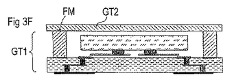
図3F:金属製のフレーム構造RSは、金属製の層を少なくとも含有する、扁平に構成された第2のハウジング部分によってカバーされ、この第2のハウジング部分に機械的に接続することができる。これは例えば錫を含有するはんだ層を介して、フレーム構造と第2のハウジング部分GT2との間で行われる。このはんだ層LSは、例えば10μmの厚さであって、Sn層を含有している。 FIG. 3F: The metal frame structure RS is covered by a flatly configured second housing part containing at least a metal layer and can be mechanically connected to this second housing part. This takes place between the frame structure and the second housing part GT2, for example via a solder layer containing tin. The solder layer LS has a thickness of, for example, 10 μm and includes an Sn layer.
基板BPも第2のハウジング部分GT2若しくは、この第2のハウジング部分GT2のために用いられたカバーも、有利には大判状であって、複数の中空室若しくは構成部分を有しているので、最後の段階でこれらの構成部分が個別化され、この際に、複数の中空室が閉じられた状態で維持されるように、一方側または両側から、ハウジング部分に切り込みが入れられる。ウェーハ平面上に形成された閉じたハウジングの個別化は、鋸引きによって、レーザ微細加工によってまたはフライス切削によって行われる。 Since the substrate BP and the second housing part GT2 or the cover used for this second housing part GT2 are also advantageously large and have a plurality of hollow chambers or components, In the last stage, these components are individualized, in which case the housing part is cut from one or both sides so that the plurality of cavities are kept closed. The individualization of the closed housing formed on the wafer plane is done by sawing, by laser micromachining or by milling.
図4には、第1実施例および第2実施例とは異なり、予め形成された切欠を備えた、第1のハウジング部分GT1を形成する基板が使用されている第4実施例による構成部分の製造法について示されている。この場合、犠牲層OSおよび、これによって微細加工されたホルダHAを切欠内に形成する必要がある。第1のハウジング部分GT1の側壁SWおよび底板BPは、有利には同じ誘電材料より成っている。ホルダの製造と一緒に、金属被覆FMは、少なくとも接合面を形成する、表面の領域に被着される。この領域は切欠をフレーム状に包囲している。この場合、金属被覆は、例えば図4Fに示されているように、切欠の底部および内壁の部分も被覆している。阻止チップの載設および犠牲層の取り除きは、別の実施例において説明されているように行われる。第2のハウジング部分GT2は、第2実施例と同様に選択され、かつ被着される。図4Fは、金属被覆が接合面上にも、また内壁にも、および部分的に切欠の底部上に被着されている基板を示している。この場合、図4Fの右に示されているように(符号bの場合)、接合面上の金属被覆FMを、側壁の内側面の金属被覆から電気的に分離することができる。図4Fの左側において(符号aの場合)、金属被覆は、接合面および側壁の領域内で一体的であるか若しくは中断されていない。 In FIG. 4, unlike the first and second embodiments, the components according to the fourth embodiment in which the substrate forming the first housing part GT <b> 1 with a pre-formed notch is used. The manufacturing method is shown. In this case, it is necessary to form the sacrificial layer OS and the finely processed holder HA in the notch. The side wall SW and the bottom plate BP of the first housing part GT1 are preferably made of the same dielectric material. Along with the manufacture of the holder, the metal coating FM is applied to the area of the surface that forms at least the joining surface. This region surrounds the notch in a frame shape. In this case, the metal coating also covers the bottom and inner wall portions of the notch, for example as shown in FIG. 4F. Placement of the blocking tip and removal of the sacrificial layer is performed as described in another embodiment. The second housing part GT2 is selected and deposited in the same way as in the second embodiment. FIG. 4F shows the substrate with metallization deposited on the joining surface as well as on the inner wall and partially on the bottom of the notch. In this case, as shown on the right side of FIG. 4F (in the case of reference sign b), the metal coating FM on the joining surface can be electrically separated from the metal coating on the inner side surface of the side wall. On the left side of FIG. 4F (in the case of symbol a), the metal coating is either integral or uninterrupted in the area of the joining surface and the side walls.
第1のハウジング部分と第2のハウジング部分との接続がはんだ付けによって行われる場合、図4Fの右側(符号bの場合)に示されているように、接合面上の金属被覆と切欠の内側面における金属被覆とを分離するか、またははんだによって濡らすことができないストッパ層を接合面と内側面との移行部に設ければ有利である。これによって、第1のハウジング部分と第2のハウジング部分とをはんだ付けによって接続する際に、はんだは接合面の接続領域において保持され、この接続領域から出ることは避けられる。 When the connection between the first housing part and the second housing part is made by soldering, as shown on the right side of FIG. It is advantageous if a stopper layer that cannot be separated from the metal coating on the side or wetted by solder is provided at the transition between the joining surface and the inner surface. As a result, when the first housing part and the second housing part are connected by soldering, the solder is held in the connection area of the joint surface and is prevented from exiting from this connection area.
切欠の内室の少なくとも部分的な金属製の被覆部によって、切欠を仕切る側壁を、ガスまたは湿気を通す材料より製造することができる。この金属被覆によって、高級なシールが得られ、このシールによって、第1のハウジング部分GT1の基板(台板)と側壁(フレーム構造部)との間の制限面もシールすることができる。 By means of at least a partial metal covering of the inner chamber of the notch, the side walls that partition the notch can be made from a material that allows gas or moisture to pass through. A high-grade seal is obtained by this metal coating, and the limiting surface between the substrate (base plate) and the side wall (frame structure portion) of the first housing portion GT1 can also be sealed by this seal.
金属被覆は、フレーム構造が基板上に接着される構成のためにも有利である。金属被覆は、少なくとも部分的に、スパッターまたは蒸着等のPVD法で被着することができる。有利な形式で、PVD法は、電気めっきまたは無電流の金属析出と組み合わせることができる。接着層として用いられる最も下の層は、例えば50nmのTiおよびその上側に200nmのCuを有することができる。 Metallization is also advantageous for configurations where the frame structure is bonded onto the substrate. The metal coating can be applied at least partially by PVD methods such as sputtering or evaporation. In an advantageous manner, the PVD method can be combined with electroplating or currentless metal deposition. The bottom layer used as an adhesion layer can have, for example, 50 nm of Ti and 200 nm of Cu above it.
ホルダ、機械式のフレーム構造および/または金属製の、中空室の被覆部は、それぞれ所望の層厚で最適には電気めっき式に製造される。経済的なおよび/または技術的な理由により、種々異なる機能エレメントのための、種々異なる材料厚さおよび/または種々異なる金属、例えば種々異なる表面層を有する共通のベースメタルが有利である。したがって、電気めっきのために必要な接続部は、種々異なる機能エレメントのために個別の電気めっき段階を実施することができるように、構成されている。したがって、たとえば、所定の機能エレメントのためだけに必要な金属層(例えばスタッドバンプによるAuコーティング)が、別の機能エレメントにおいても生ぜしめられる。 The holders, the mechanical frame structure and / or the metal hollow chamber coverings are each optimally electroplated with the desired layer thickness. For economic and / or technical reasons, a common base metal with different material thicknesses and / or different metals, eg different surface layers, for different functional elements is advantageous. The connections required for electroplating are thus configured so that individual electroplating steps can be performed for different functional elements. Thus, for example, a metal layer that is necessary only for a given functional element (eg Au coating with stud bumps) is also produced in another functional element.
本発明の有利な実施例では、構成素子がホルダ上に載せられてこのホルダに結合される前に、構成部分を製造する際に、ホルダの製造後に犠牲層が取り除かれる。構成素子とホルダとの間の堅牢な電気的および機械的な結合は、犠牲層を取り除いた後でも次のようにして得られる。つまり、構成素子との結合のために設けられた、切欠の底部に対する間隔hを有する、ホルダの第2の領域が、結合が形成されるまで、載設力によって底部上に押し付けられることによって、得られる。このためにホルダの弾性的な変形可能性が利用される。このようなホルダの弾性的な変形可能性によって、構成素子との結合後に引き続き再びその初期の位置若しくは形状に戻るようになっているので、ボンディングされた構成素子が再び、切欠の底部に対するおよびひいては下側の第1のハウジング部分に対する相応の所望間隔hを保って配置される。この変化例のために、ボンディング法として例えばサーモソニック・ボンディングが用いられる。 In an advantageous embodiment of the invention, the sacrificial layer is removed after the holder is manufactured in manufacturing the component before the component is mounted on the holder and bonded to the holder. A robust electrical and mechanical connection between the component and the holder is obtained as follows even after the sacrificial layer is removed. That is, the second region of the holder, which is provided for coupling with the component and has a distance h to the bottom of the notch, is pressed onto the bottom by the mounting force until the coupling is formed, can get. For this purpose, the elastic deformability of the holder is used. Due to the elastic deformability of the holder, it is possible to continue to return to its initial position or shape after connection with the component, so that the bonded component is again against the bottom of the notch and thus It is arranged with a corresponding desired spacing h with respect to the lower first housing part. For this variation, for example, thermosonic bonding is used as the bonding method.
図5に示した方法においては、1つの構成素子ウェーハに互いに平行に形成される、シート状の複数の構成素子チップは、適切な構成素子間隔もしくは適切なラスタ(Raster)を保って前もって固定された複数の構成素子の配置が得られるように、個別化される。このために、裏側に電気的な接続部を有していない構成素子が、補助担体HF上に、有利にはいわゆるUV剥離シート(UV-Release-Folie)上に接着される。次いで、構成素子ウェーハは、シートを分離することなしに前側から鋸によって切り離される。 In the method shown in FIG. 5, a plurality of sheet-like component chips formed in parallel to each other on one component wafer are fixed in advance while maintaining an appropriate component spacing or an appropriate raster (Raster). Individualized so as to obtain an arrangement of a plurality of components. For this purpose, the components that do not have an electrical connection on the back side are glued on the auxiliary carrier HF, preferably on a so-called UV-Release-Folie. The component wafer is then cut off from the front side by sawing without separating the sheets.
UV剥離シートにおいて、UV作用によって接着作用は著しく低下され、事実上接着作用はなくなる。この作用は、このような補助シートHF上に接着された構成素子の表側が別の補助シートに接着されることによって、利用される。この場合、所望の構成素子の接着作用は、UV剥離シートの裏側を所望に露光することによって無効にされる。補助シートを引き剥がすことによって、UV剥離シートに対する接着作用が低下されたチップだけが第2の補助シート上に移される。 In the UV release sheet, the adhesive action is remarkably reduced by the UV action, and the adhesive action is virtually eliminated. This effect is utilized by adhering the front side of the component adhered on such an auxiliary sheet HF to another auxiliary sheet. In this case, the adhesive action of the desired component is nullified by exposing the back side of the UV release sheet as desired. By peeling off the auxiliary sheet, only the chips with reduced adhesion to the UV release sheet are transferred onto the second auxiliary sheet.
このような形式で、図5に示されているように、1回の段階で互いに間隔を保っているだけのチップをそれぞれ、第2の補助シート上に接着することができる。1回の段階でX方向でもY方向でもそれぞれ2番目の構成素子が移されるラスタが選択されると、構成素子ウェーハ上の複数の構成素子の密集したパッケージが4回の段階で、4つの配置若しくは4つの補助シート上に移され、これらの4つの配置若しくは4つの補助シートにおいて、それぞれ初期の構成素子密度の1/4だけが、相応の間隔を保ってX方向およびY方向に位置している。このようにして得られた、第2の補助シート上に接着された構成素子間の間隔は、第2の補助シートを構成素子と共に図5に示した方法で直接設置するために、十分である。この個別化法によって、第2の補助シート上に接着された構成素子を、より大きい間隔を保って設けることも可能であるが、この場合は、この方法によって、間隔はそれぞれ構成素子幅の整数倍に調整されるだけである。これがハウジング部分の寸法規定のために不都合である場合には、構成素子は個別に所望のラスタ内で補助シート上に配置することができる。 In this manner, as shown in FIG. 5, chips that are only spaced apart from each other in one step can be bonded onto the second auxiliary sheet. When a raster to which the second component is transferred in both the X and Y directions in one step is selected, a dense package of a plurality of components on the component wafer is arranged in four steps in four steps. Or on these four auxiliary sheets, in these four arrangements or four auxiliary sheets, only ¼ of the initial component density is respectively located in the X and Y directions with corresponding spacing. Yes. The spacing between the components bonded on the second auxiliary sheet thus obtained is sufficient to directly install the second auxiliary sheet together with the components in the manner shown in FIG. . By this individualization method, it is possible to provide the constituent elements bonded on the second auxiliary sheet with a larger spacing, but in this case, the spacing is an integer number of the constituent element widths. It is only adjusted by a factor of two. If this is inconvenient due to the sizing of the housing part, the components can be individually placed on the auxiliary sheet in the desired raster.
種々異なる構成素子が1つの共通のハウジング内に組み込まれる場合には、種々異なる構成素子が同じ形式または類似の形式で1つの共通の補助担体上に取り付けられる。場合によっては、個別化の前記プロセスを、ラスタ間隔を大きくしながらそれぞれの構成素子型式のために個別に実施する必要がある。次いで最後の段階で、種々異なる構成素子を1つの共通の補助担体上でまとめる作業が行われる。 If the different components are integrated in one common housing, the different components are mounted on one common auxiliary carrier in the same or similar manner. In some cases, the individualization process may need to be performed separately for each component type while increasing the raster spacing. The last step is then to work the different components together on one common auxiliary carrier.
個別化のその他の有利な可能性は、2つの段階を利用するという点にある。この場合、第1の段階で構成素子の表側から構成素子ウェーハに切り込みが入れられる。次いで構成素子ウェーハはその表側が接着シートまたは補助担体上にもたらされ、目引きが露出されそれによって各構成素子が個別化されるまで、裏側から研磨される。次いで構成素子はその裏側が例えばいわゆる剥離シート上に移される。この方法段階は、構成素子が、方法の最後に用いられた、コンタクト面に向き合う裏側を有する補助シート上に載せられるように、行われる。 Another advantageous possibility of individualization is that it uses two stages. In this case, in the first stage, the component wafer is cut from the front side of the component. The component wafer is then polished from the backside until its front side is brought onto an adhesive sheet or auxiliary carrier and the stitches are exposed, thereby individualizing each component. The component is then transferred on its back side, for example on a so-called release sheet. This method step is carried out so that the component is placed on the auxiliary sheet used at the end of the method and having the back side facing the contact surface.
本発明は図示の実施例および図面だけに限定されるものではない。むしろ、特別に構成されたホルダを、公知である中空室ハウジングと組み合わせることができる。この場合、構成素子を残留応力なしに組み込むことができるので、構成素子は、強い熱的および機械的な交番負荷(Wechselbelastung)にさらされた場合でも、その特性が許容できない程度に変化することなしに確実に駆動することができる。本発明によって提案された構成部分は、特定の型式の構成素子だけに限定さるものではなく、機械的な応力に対する高い感度を有する種々異なる形式の多数のチップのミニチュア化されたハウジングが可能である。本発明はまた、ガス、湿気または化学物質の侵入を確実に阻止する気密なシールの可能性を提供する。中空室内に保護ガスを設けることによって構成素子の保護を促進することができる。さらにまた、有機的な物質に対して完全に保護された内部を有する構成素子ハウジングが得られる。何故ならば、中空室内に残留するすべての成分は無機的な天然物質だからである。汚染され易い構成素子チップは、このようにして蒸発した成分に対して保護される。 The present invention is not limited to the illustrated embodiments and drawings. Rather, specially constructed holders can be combined with known hollow chamber housings. In this case, the component can be incorporated without residual stress, so that the component does not change unacceptably even when subjected to strong thermal and mechanical alternating loads (Wechselbelastung). Can be reliably driven. The components proposed by the present invention are not limited to specific types of components, but can be miniaturized housings of multiple different types of chips with high sensitivity to mechanical stress. . The present invention also offers the possibility of an airtight seal that reliably prevents the ingress of gas, moisture or chemicals. By providing a protective gas in the hollow chamber, protection of the constituent elements can be promoted. Furthermore, a component housing having an interior that is completely protected against organic substances is obtained. This is because all components remaining in the hollow chamber are inorganic natural substances. Contaminant component chips are thus protected against evaporated components.
構成部分を製造するための本発明のすべての方法において、ホルダを微細加工するための犠牲層を設けることができ、この場合、基板表面から削除された若しくは基板表側に対して間隔を保って配置された領域が利用される。また、犠牲層を取り除く前にボンディングが行われるようになっていれば、構成素子を犠牲層によって構成素子の前記領域に接続する作業が促進される。この場合、ホルダの削除された領域は、この領域の下に配置された犠牲層によって保護される。この方法では、このようなハウジング部分上にホルダおよび金属被覆を同時に生ぜしめるために、種々異なる金属被覆段階が用いられる。金属製のフレーム構造を製造する場合においても、構成部分の別の金属被覆を生ぜしめるために、金属被覆法が交互におよび同時に用いられる。本発明によって提案された構成部分によって、種々異なる多数の構成素子および特にMEMS構成素子のためのハウジングプラットフォームを設けることも可能である。このために従来では、それぞれ構成素子に特別に適合させたハウジングが必要であった。本発明によれば、事実上すべての同じような製品のための安価なプラットフォームが形成される。 In all the methods of the invention for manufacturing the components, a sacrificial layer for microfabrication of the holder can be provided, in which case it has been removed from the substrate surface or placed at a distance from the substrate front side Area is used. If bonding is performed before the sacrifice layer is removed, the operation of connecting the component element to the region of the component element by the sacrifice layer is facilitated. In this case, the removed area of the holder is protected by a sacrificial layer located below this area. In this method, different metallization stages are used to simultaneously produce a holder and metallization on such a housing part. Even in the production of metal frame structures, metallization methods are used alternately and simultaneously to produce another metallization of the components. Depending on the components proposed by the invention, it is also possible to provide a number of different components and in particular a housing platform for MEMS components. For this reason, conventionally, a housing specially adapted to each component has been required. According to the present invention, an inexpensive platform for virtually all similar products is formed.
BE 機械反応式に構成素子、チップ
GT1,GT2 ハウジング部分
HA ホルダ
DM シール手段、例えば接着剤
HT 補助担体
KF チップ上の接点面
AF 基板上の接続面
DK スルーコンタクト
LK はんだ付け可能な(外側)接点
FM 接合面金属化
h エアギャップの高さ
WH 別の金属化
BU バンプ
BP 台板(ベッドプレート)
LM はんだマスク
OS 犠牲層
GM 接合面における基板金属化
RS フレーム構造
LS はんだ層
BE Mechanically reactive component, chip GT1, GT2 Housing part HA holder DM Sealing means, eg adhesive HT Auxiliary carrier KF Contact surface on chip AF Connection surface on substrate DK Through contact LK Solderable (outside) contact FM Metallization of joint surface h Air gap height WH Other metallization BU Bump BP Base plate (bed plate)
LM solder mask OS sacrificial layer GM substrate metallization at joint surface RS frame structure LS solder layer
Claims (34)
第1のハウジング部分と第2のハウジング部分とを備えていて、前記第1のハウジング部分と前記第2のハウジング部分とが接合面を介して互いに堅固に結合されており、
第1のハウジング部分(GT1)内に設けられた切欠を備えていて、該切欠の底部に接続面が設けられていて、該切欠が中空室(HS)を形成して前記第2のハウジング部分によって閉鎖されており、
前記構成素子(BE)がチップを有していて、該チップが表面上に接点面を有しており、
前記構成素子が、弾性的または塑性変形可能な、導電性のホルダ(HA)によって前記中空室内に懸架されており、該ホルダが前記接点面のうちの1つを前記接続面のうちの1つに接続する、
ことを特徴とする、機械的に敏感な電子構成素子のための中空室を備えた構成部分。 In a component with a hollow chamber for a mechanically sensitive electronic component (BE),
A first housing part and a second housing part, wherein the first housing part and the second housing part are firmly connected to each other via a joint surface;
The second housing part has a notch provided in the first housing part (GT1), a connection surface is provided at the bottom of the notch, and the notch forms a hollow chamber (HS). Closed by
The component (BE) has a chip, and the chip has a contact surface on the surface;
The component is suspended in the hollow chamber by a conductive holder (HA) that can be elastically or plastically deformed, and the holder can connect one of the contact surfaces to one of the connection surfaces. Connect to the
A component with a hollow chamber for mechanically sensitive electronic components, characterized in that
前記ホルダがそれぞれ1つの第1の領域を介して、底部上に配置された電気的な接続面(AF)に接続されており、
前記ホルダが前記底部上でそれぞれ第2の領域に向かって上昇しており、
前記構成素子(BE)がその接点面を介して、前記底部と第2の領域との間にエアギャップが残存するように、ホルダのそれぞれ第2の領域に接続されている、請求項1から5までのいずれか1項記載の構成部分。 The holder extends longitudinally between the two regions, parallel to the bottom of one housing part (GT),
Each of the holders is connected to an electrical connection surface (AF) arranged on the bottom via a first region,
The holders are respectively raised on the bottom toward the second region;
From the contact area, the component (BE) is connected to each second region of the holder such that an air gap remains between the bottom and the second region. 5. The component according to any one of 5 to 5.
接合面で互いに合致し合うように構成され、かつ接合面で互いに結合されて、内部に中空室を形成するように、成形された2つのケーシング部分(GT1,GT2)を準備し、この場合、第1のハウジング部分に外部に取り付けられたはんだ付け可能な接点を設け、該接点を、スルーコンタクトを介して、前記第1のハウジング部分(GT1)の底部(BO)上の、前記中空室側に面した接点面に接続し、
第1のハウジング部分の底部上に犠牲層(OS)を被着し、かつ微細加工し、
微細加工された金属層を被着してホルダ(HA)を形成し、この場合、該ホルダ(HA)のそれぞれ1つの第1の領域が接点面に接続され、かつこの第1の領域から離れた第2の領域が、微細加工された犠牲層上に配置されるようにし、
構成素子を、前記ホルダの第2の領域に載設し、かつ接続し、
この接続前にまたは接続後に犠牲層を取り除き、この際に、構成素子に接続された、ホルダの領域と第1のハウジング部分の底部との間にエアギャップ(SP)を残す、
という方法段階を有することを特徴とする、機械的に敏感な電気構成素子(BE)のための中空室を備えた電気的な構成部分を製造するための方法。 In a method for manufacturing an electrical component with a hollow chamber for a mechanically sensitive electrical component (BE),
Preparing two casing parts (GT1, GT2) which are configured to mate with each other at the joining surface and are joined to each other at the joining surface to form a hollow chamber therein; A solderable contact externally attached to the first housing part is provided, and the contact is connected to the hollow chamber side on the bottom (BO) of the first housing part (GT1) via a through contact. Connected to the contact surface facing
Depositing a sacrificial layer (OS) on the bottom of the first housing part and micromachining;
A microfabricated metal layer is deposited to form a holder (HA), wherein each first region of the holder (HA) is connected to the contact surface and away from the first region. The second region is disposed on the microfabricated sacrificial layer;
Mounting and connecting the component to the second region of the holder;
Removing the sacrificial layer before or after this connection, leaving an air gap (SP) between the region of the holder connected to the component and the bottom of the first housing part,
A method for manufacturing an electrical component with a hollow chamber for a mechanically sensitive electrical component (BE), characterized in that it comprises the following process steps:
前記2つのハウジング部分(GT1,GT2)を気密に結合する、請求項24記載の方法。 Placing the second housing part (GT2) on the first housing part (GT1);
25. Method according to claim 24, wherein the two housing parts (GT1, GT2) are hermetically joined.
第2の大判状のハウジング部分(GTW2)を提供し、
すべての切欠のためのホルダを、1回の共通の方法段階で切欠内に形成し、
構成素子(BE)を第1のハウジング部分ウェーハ(GTW1)の切欠内に設置して、前記ホルダに固定し、
第1のハウジング部分ウェーハ(GTW1)と大判状のハウジング部分(GTW2)とを、前記切欠内で構成素子(BE)を包囲するように結合し、
結合されたハウジング部分(GTW1,GTW2)をそれぞれ1対形式で結合された第1のハウジング部分と第2のハウジング部分とに分けて、気密に包囲された、個別の構成素子(BE)、またはグループを形成する構成素子(BE)を有する構成部分を提供する、
請求項24または25記載の方法。 Providing a first large-sized housing wafer having a plurality of notches formed in advance in the housing wafer;
Providing a second large-sized housing part (GTW2);
Forming a holder for all notches in the notch in one common method step,
The component (BE) is installed in the notch of the first housing partial wafer (GTW1) and fixed to the holder,
A first housing part wafer (GTW1) and a large-sized housing part (GTW2) are joined so as to surround the component (BE) in the notch,
Individual components (BE) hermetically surrounded by separating the combined housing parts (GTW1, GTW2) into a first housing part and a second housing part, which are respectively connected in a paired manner, or Providing a component having a component (BE) forming a group;
26. A method according to claim 24 or 25.
構成素子を、犠牲層およびこの犠牲層上に部分的に設けられたホルダと共に、接続面上に載せ、
次いで犠牲層を取り除き、この際に、構成素子に接続された、ホルダの端部と、第1のハウジング部分の底部との間にエアギャップ(SP)を残す、請求項24から32までのいずれか1項記載の方法。 The sacrificial layer and the holder according to the modification of claim 22, wherein the sacrificial layer and the holder are formed on the front side of the component supporting the contact surface
The component is mounted on the connection surface together with a sacrificial layer and a holder partially provided on the sacrificial layer,
The sacrificial layer is then removed, leaving an air gap (SP) between the end of the holder connected to the component and the bottom of the first housing part. The method according to claim 1.
Applications Claiming Priority (2)
| Application Number | Priority Date | Filing Date | Title |
|---|---|---|---|
| DE102005050398A DE102005050398A1 (en) | 2005-10-20 | 2005-10-20 | Cavity housing for a mechanically sensitive electronic device and method of manufacture |
| PCT/DE2006/001736 WO2007045204A1 (en) | 2005-10-20 | 2006-09-29 | Housing with a cavity for a mechanically-sensitive electronic component and method for production |
Publications (2)
| Publication Number | Publication Date |
|---|---|
| JP2009512369A true JP2009512369A (en) | 2009-03-19 |
| JP2009512369A5 JP2009512369A5 (en) | 2012-08-02 |
Family
ID=37758890
Family Applications (1)
| Application Number | Title | Priority Date | Filing Date |
|---|---|---|---|
| JP2008535876A Pending JP2009512369A (en) | 2005-10-20 | 2006-09-29 | Housing with hollow chamber for mechanically sensitive electronic components and method for manufacturing the housing |
Country Status (4)
| Country | Link |
|---|---|
| US (1) | US20090127697A1 (en) |
| JP (1) | JP2009512369A (en) |
| DE (2) | DE102005050398A1 (en) |
| WO (1) | WO2007045204A1 (en) |
Cited By (2)
| Publication number | Priority date | Publication date | Assignee | Title |
|---|---|---|---|---|
| JP2016525946A (en) * | 2013-05-24 | 2016-09-01 | エプコス アクチエンゲゼルシャフトEpcos Ag | Microelectromechanical system device package and method for manufacturing microelectromechanical system device package |
| JP7401200B2 (en) | 2019-06-14 | 2023-12-19 | 太陽誘電株式会社 | Electronic device manufacturing method |
Families Citing this family (37)
| Publication number | Priority date | Publication date | Assignee | Title |
|---|---|---|---|---|
| DE102005008514B4 (en) * | 2005-02-24 | 2019-05-16 | Tdk Corporation | Microphone membrane and microphone with the microphone membrane |
| DE102005008512B4 (en) | 2005-02-24 | 2016-06-23 | Epcos Ag | Electrical module with a MEMS microphone |
| DE102005008511B4 (en) * | 2005-02-24 | 2019-09-12 | Tdk Corporation | MEMS microphone |
| JP2009515352A (en) * | 2005-11-09 | 2009-04-09 | コーニンクレッカ フィリップス エレクトロニクス エヌ ヴィ | Package carrier manufacturing method and diagnostic device manufacturing method for sealing at least one microelectronic device |
| DE102005053767B4 (en) * | 2005-11-10 | 2014-10-30 | Epcos Ag | MEMS microphone, method of manufacture and method of installation |
| DE102005053765B4 (en) * | 2005-11-10 | 2016-04-14 | Epcos Ag | MEMS package and method of manufacture |
| DE102007010711B4 (en) * | 2007-02-28 | 2018-07-05 | Fraunhofer-Gesellschaft zur Förderung der angewandten Forschung e.V. | Switching arrangement, measuring device with it and method for its production |
| DE102007020288B4 (en) * | 2007-04-30 | 2013-12-12 | Epcos Ag | Electrical component |
| DE102007028288B4 (en) * | 2007-06-20 | 2013-06-06 | Epcos Ag | Acoustic wave MEMS device and method of manufacture |
| DE102008028299B3 (en) | 2008-06-13 | 2009-07-30 | Epcos Ag | System support for e.g. micro-electro-mechanical system component, has flexible support with upper side, and conductor paths guided to connecting contacts on upper side of components, which is turned away from flexible support |
| WO2010077311A1 (en) * | 2008-12-17 | 2010-07-08 | Sand9, Inc. | Multi-port mechanical resonating devices and related methods |
| DE102009007837A1 (en) | 2009-02-06 | 2010-08-19 | Epcos Ag | Sensor module and method for producing sensor modules |
| JP5045769B2 (en) * | 2009-03-04 | 2012-10-10 | 株式会社デンソー | Manufacturing method of sensor device |
| DE102009002559A1 (en) * | 2009-04-22 | 2010-10-28 | Robert Bosch Gmbh | sensor arrangement |
| US20110037162A1 (en) * | 2009-07-24 | 2011-02-17 | Aeroflex Microelectronic Solutions | Hermetic packaging and method of forming the same |
| US8736388B2 (en) | 2009-12-23 | 2014-05-27 | Sand 9, Inc. | Oscillators having arbitrary frequencies and related systems and methods |
| DE102010012042A1 (en) * | 2010-03-19 | 2011-09-22 | Epcos Ag | Component with a chip in a cavity and a voltage-reduced attachment |
| DE102010054782A1 (en) | 2010-12-16 | 2012-06-21 | Epcos Ag | Housing electrical component |
| DE102010055627A1 (en) * | 2010-12-22 | 2012-06-28 | Epcos Ag | Electrical module for insertion by automatic insertion machines by generating a vacuum |
| DE102011004577B4 (en) * | 2011-02-23 | 2023-07-27 | Robert Bosch Gmbh | Component carrier, method for producing such a component carrier and component with a MEMS component on such a component carrier |
| JP2013046167A (en) * | 2011-08-23 | 2013-03-04 | Seiko Epson Corp | Vibration device and manufacturing method of vibration device |
| US8436433B1 (en) * | 2011-10-13 | 2013-05-07 | Rosemount Aerospace Inc. | Unattached contained semiconductor devices |
| DE102012108106B4 (en) * | 2012-08-31 | 2016-06-16 | Epcos Ag | MEMS component and method for manufacturing an acoustic wave MEMS device |
| DE102013100197A1 (en) * | 2013-01-10 | 2014-07-10 | Continental Automotive Gmbh | Sensing unit for motor car, has injection molded plastic carrier which is positioned on opposite side to sensor element, and formed of electrical contacts with respect to the circuit board |
| DE102013100388B4 (en) * | 2013-01-15 | 2014-07-24 | Epcos Ag | Component with a MEMS component and method of manufacture |
| DE102013103494A1 (en) * | 2013-04-08 | 2014-10-09 | Pro-Micron Gmbh & Co. Kg | Strain gauge sensor |
| DE102013106353B4 (en) * | 2013-06-18 | 2018-06-28 | Tdk Corporation | Method for applying a structured coating to a component |
| DE102014105861B4 (en) | 2014-04-25 | 2015-11-05 | Infineon Technologies Ag | Sensor device and method for producing a sensor device |
| DE102014106503B4 (en) | 2014-05-08 | 2016-03-03 | Epcos Ag | Method of making a microphone |
| DE102014008839B4 (en) * | 2014-06-20 | 2021-09-30 | Kunststoff-Zentrum In Leipzig Gemeinnützige Gmbh | Expansion-compensating connecting element for a microelectronic system |
| US10442683B2 (en) * | 2016-04-14 | 2019-10-15 | Akustica, Inc. | Corrugated package for microelectromechanical system (MEMS) device |
| WO2018009543A1 (en) * | 2016-07-07 | 2018-01-11 | Molex, Llc | Molded interconnect device and method of making same |
| US10028411B2 (en) * | 2016-07-26 | 2018-07-17 | Continental Automotive Systems, Inc. | Electronic controller with laser weld sealed housing |
| CN109935668B (en) * | 2017-12-19 | 2021-08-24 | 英属开曼群岛商錼创科技股份有限公司 | Micro-device structure |
| CN108358160B (en) * | 2018-04-18 | 2023-08-01 | 中国兵器工业集团第二一四研究所苏州研发中心 | Hoisting type MEMS device packaging structure capable of releasing stress |
| DE102019214478A1 (en) * | 2019-09-23 | 2021-03-25 | Infineon Technologies Ag | PHOTOACOUSTIC GAS SENSOR |
| US11616027B2 (en) | 2019-12-17 | 2023-03-28 | Analog Devices International Unlimited Company | Integrated circuit packages to minimize stress on a semiconductor die |
Citations (6)
| Publication number | Priority date | Publication date | Assignee | Title |
|---|---|---|---|---|
| JPH05299963A (en) * | 1992-04-20 | 1993-11-12 | Kyocera Corp | Electronic parts housing container |
| JPH07297667A (en) * | 1994-04-22 | 1995-11-10 | Citizen Watch Co Ltd | Surface mounted type piezoelectric vibrator |
| JPH09153762A (en) * | 1995-11-30 | 1997-06-10 | Daishinku Co | Surface-mount type piezoelectric vibrator |
| JPH1126628A (en) * | 1997-06-30 | 1999-01-29 | Murata Mfg Co Ltd | Package structure of electronic component |
| JP2004088566A (en) * | 2002-08-28 | 2004-03-18 | Nippon Dempa Kogyo Co Ltd | Crystal oscillator |
| JP2005244642A (en) * | 2004-02-26 | 2005-09-08 | Kyocera Corp | Piezoelectric oscillator |
Family Cites Families (61)
| Publication number | Priority date | Publication date | Assignee | Title |
|---|---|---|---|---|
| US3587322A (en) * | 1969-06-17 | 1971-06-28 | Simmonds Precision Products | Pressure transducer mounting |
| US4454440A (en) * | 1978-12-22 | 1984-06-12 | United Technologies Corporation | Surface acoustic wave (SAW) pressure sensor structure |
| US4424419A (en) * | 1981-10-19 | 1984-01-03 | Northern Telecom Limited | Electret microphone shield |
| US4545440A (en) * | 1983-04-07 | 1985-10-08 | Treadway John E | Attachment for pneumatic hammers for punching holes of varying size |
| US5091051A (en) * | 1986-12-22 | 1992-02-25 | Raytheon Company | Saw device method |
| US5216490A (en) * | 1988-01-13 | 1993-06-01 | Charles Stark Draper Laboratory, Inc. | Bridge electrodes for microelectromechanical devices |
| US4866683A (en) * | 1988-05-24 | 1989-09-12 | Honeywell, Inc. | Integrated acoustic receiver or projector |
| US5184107A (en) * | 1991-01-28 | 1993-02-02 | Honeywell, Inc. | Piezoresistive pressure transducer with a conductive elastomeric seal |
| US5650685A (en) * | 1992-01-30 | 1997-07-22 | The United States Of America As Represented By The Secretary Of The Army | Microcircuit package with integrated acoustic isolator |
| JP3328102B2 (en) * | 1995-05-08 | 2002-09-24 | 松下電器産業株式会社 | Surface acoustic wave device and method of manufacturing the same |
| US6033935A (en) * | 1997-06-30 | 2000-03-07 | Formfactor, Inc. | Sockets for "springed" semiconductor devices |
| US5573435A (en) * | 1995-08-31 | 1996-11-12 | The Whitaker Corporation | Tandem loop contact for an electrical connector |
| TW332166B (en) * | 1995-10-06 | 1998-05-21 | Laurance Lewellin Richard | Method for making articles with rice hulls |
| US5674785A (en) * | 1995-11-27 | 1997-10-07 | Micron Technology, Inc. | Method of producing a single piece package for semiconductor die |
| WO1997050127A1 (en) * | 1996-06-24 | 1997-12-31 | International Business Machines Corporation | Stacked semiconductor device package |
| US5990418A (en) * | 1997-07-29 | 1999-11-23 | International Business Machines Corporation | Hermetic CBGA/CCGA structure with thermal paste cooling |
| TW387198B (en) * | 1997-09-03 | 2000-04-11 | Hosiden Corp | Audio sensor and its manufacturing method, and semiconductor electret capacitance microphone using the same |
| US6150753A (en) * | 1997-12-15 | 2000-11-21 | Cae Blackstone | Ultrasonic transducer assembly having a cobalt-base alloy housing |
| DE19806818C1 (en) * | 1998-02-18 | 1999-11-04 | Siemens Matsushita Components | Method for producing an electronic component, in particular an SAW component working with acoustic surface waves |
| US6400065B1 (en) * | 1998-03-31 | 2002-06-04 | Measurement Specialties, Inc. | Omni-directional ultrasonic transducer apparatus and staking method |
| FI105880B (en) * | 1998-06-18 | 2000-10-13 | Nokia Mobile Phones Ltd | Fastening of a micromechanical microphone |
| US6732588B1 (en) * | 1999-09-07 | 2004-05-11 | Sonionmems A/S | Pressure transducer |
| US6829131B1 (en) * | 1999-09-13 | 2004-12-07 | Carnegie Mellon University | MEMS digital-to-acoustic transducer with error cancellation |
| FR2799883B1 (en) * | 1999-10-15 | 2003-05-30 | Thomson Csf | METHOD OF ENCAPSULATING ELECTRONIC COMPONENTS |
| EP1230739B1 (en) * | 1999-11-19 | 2016-05-25 | Gentex Corporation | Vehicle accessory microphone |
| US6324907B1 (en) * | 1999-11-29 | 2001-12-04 | Microtronic A/S | Flexible substrate transducer assembly |
| US20020076910A1 (en) * | 1999-12-15 | 2002-06-20 | Pace Benedict G. | High density electronic interconnection |
| US6613605B2 (en) * | 1999-12-15 | 2003-09-02 | Benedict G Pace | Interconnection method entailing protuberances formed by melting metal over contact areas |
| US6236145B1 (en) * | 2000-02-29 | 2001-05-22 | Cts Corporation | High thermal resistivity crystal resonator support structure and oscillator package |
| JP2001267473A (en) * | 2000-03-17 | 2001-09-28 | Hitachi Ltd | Semiconductor device and its manufacturing method |
| US6809413B1 (en) * | 2000-05-16 | 2004-10-26 | Sandia Corporation | Microelectronic device package with an integral window mounted in a recessed lip |
| US6856225B1 (en) * | 2000-05-17 | 2005-02-15 | Xerox Corporation | Photolithographically-patterned out-of-plane coil structures and method of making |
| US6569754B2 (en) * | 2000-08-24 | 2003-05-27 | The Regents Of The University Of Michigan | Method for making a module including a microplatform |
| US6530515B1 (en) * | 2000-09-26 | 2003-03-11 | Amkor Technology, Inc. | Micromachine stacked flip chip package fabrication method |
| US7434305B2 (en) * | 2000-11-28 | 2008-10-14 | Knowles Electronics, Llc. | Method of manufacturing a microphone |
| US7166910B2 (en) * | 2000-11-28 | 2007-01-23 | Knowles Electronics Llc | Miniature silicon condenser microphone |
| US7439616B2 (en) * | 2000-11-28 | 2008-10-21 | Knowles Electronics, Llc | Miniature silicon condenser microphone |
| US7092539B2 (en) * | 2000-11-28 | 2006-08-15 | University Of Florida Research Foundation, Inc. | MEMS based acoustic array |
| GB2386030B (en) * | 2000-12-22 | 2004-08-18 | Bruel & Kjaer Sound & Vibratio | A micromachined capacitive transducer |
| US6448697B1 (en) * | 2000-12-28 | 2002-09-10 | Cts Corporation | Piezoelectric device having increased mechanical compliance |
| CA2436484C (en) * | 2001-02-14 | 2008-01-22 | Gentex Corporation | Vehicle accessory microphone |
| TW554498B (en) * | 2001-08-17 | 2003-09-21 | Citizen Watch Co Ltd | Electronic device and production process thereof |
| US6930364B2 (en) * | 2001-09-13 | 2005-08-16 | Silicon Light Machines Corporation | Microelectronic mechanical system and methods |
| US7146016B2 (en) * | 2001-11-27 | 2006-12-05 | Center For National Research Initiatives | Miniature condenser microphone and fabrication method therefor |
| US6649446B1 (en) * | 2001-11-29 | 2003-11-18 | Clarisay, Inc. | Hermetic package for multiple contact-sensitive electronic devices and methods of manufacturing thereof |
| DE10164502B4 (en) * | 2001-12-28 | 2013-07-04 | Epcos Ag | Method for the hermetic encapsulation of a component |
| US6800987B2 (en) * | 2002-01-22 | 2004-10-05 | Measurement Specialties, Inc. | Protective housing for ultrasonic transducer apparatus |
| JP3908059B2 (en) * | 2002-02-27 | 2007-04-25 | スター精密株式会社 | Electret condenser microphone |
| US6627814B1 (en) * | 2002-03-22 | 2003-09-30 | David H. Stark | Hermetically sealed micro-device package with window |
| US7217588B2 (en) * | 2005-01-05 | 2007-05-15 | Sharp Laboratories Of America, Inc. | Integrated MEMS packaging |
| US7072482B2 (en) * | 2002-09-06 | 2006-07-04 | Sonion Nederland B.V. | Microphone with improved sound inlet port |
| US6781231B2 (en) * | 2002-09-10 | 2004-08-24 | Knowles Electronics Llc | Microelectromechanical system package with environmental and interference shield |
| JP3826875B2 (en) * | 2002-10-29 | 2006-09-27 | セイコーエプソン株式会社 | Piezoelectric device and manufacturing method thereof |
| US7244125B2 (en) * | 2003-12-08 | 2007-07-17 | Neoconix, Inc. | Connector for making electrical contact at semiconductor scales |
| JP3966237B2 (en) * | 2003-06-19 | 2007-08-29 | セイコーエプソン株式会社 | Piezoelectric devices and electronic devices equipped with piezoelectric devices |
| JP4264103B2 (en) * | 2004-03-03 | 2009-05-13 | パナソニック株式会社 | Electret condenser microphone |
| JP3875240B2 (en) * | 2004-03-31 | 2007-01-31 | 株式会社東芝 | Manufacturing method of electronic parts |
| JP3998658B2 (en) * | 2004-04-28 | 2007-10-31 | 富士通メディアデバイス株式会社 | Elastic wave device and package substrate |
| US7157836B2 (en) * | 2004-10-19 | 2007-01-02 | Seiko Epson Corporation | Piezoelectric device |
| DE202005001559U1 (en) * | 2005-01-31 | 2005-05-19 | Microelectronic Packaging Dresden Gmbh | Chip structure for stress-prone chips especially for sensor chips mounted on wiring carrier, provides mechanical or acoustic coupling of chip for bonding process |
| DE102005046008B4 (en) * | 2005-09-26 | 2007-05-24 | Infineon Technologies Ag | Semiconductor sensor component with sensor chip and method for producing the same |
-
2005
- 2005-10-20 DE DE102005050398A patent/DE102005050398A1/en not_active Withdrawn
-
2006
- 2006-09-29 DE DE112006002336T patent/DE112006002336A5/en not_active Withdrawn
- 2006-09-29 US US12/090,529 patent/US20090127697A1/en not_active Abandoned
- 2006-09-29 JP JP2008535876A patent/JP2009512369A/en active Pending
- 2006-09-29 WO PCT/DE2006/001736 patent/WO2007045204A1/en active Application Filing
Patent Citations (6)
| Publication number | Priority date | Publication date | Assignee | Title |
|---|---|---|---|---|
| JPH05299963A (en) * | 1992-04-20 | 1993-11-12 | Kyocera Corp | Electronic parts housing container |
| JPH07297667A (en) * | 1994-04-22 | 1995-11-10 | Citizen Watch Co Ltd | Surface mounted type piezoelectric vibrator |
| JPH09153762A (en) * | 1995-11-30 | 1997-06-10 | Daishinku Co | Surface-mount type piezoelectric vibrator |
| JPH1126628A (en) * | 1997-06-30 | 1999-01-29 | Murata Mfg Co Ltd | Package structure of electronic component |
| JP2004088566A (en) * | 2002-08-28 | 2004-03-18 | Nippon Dempa Kogyo Co Ltd | Crystal oscillator |
| JP2005244642A (en) * | 2004-02-26 | 2005-09-08 | Kyocera Corp | Piezoelectric oscillator |
Cited By (2)
| Publication number | Priority date | Publication date | Assignee | Title |
|---|---|---|---|---|
| JP2016525946A (en) * | 2013-05-24 | 2016-09-01 | エプコス アクチエンゲゼルシャフトEpcos Ag | Microelectromechanical system device package and method for manufacturing microelectromechanical system device package |
| JP7401200B2 (en) | 2019-06-14 | 2023-12-19 | 太陽誘電株式会社 | Electronic device manufacturing method |
Also Published As
| Publication number | Publication date |
|---|---|
| WO2007045204A1 (en) | 2007-04-26 |
| US20090127697A1 (en) | 2009-05-21 |
| DE102005050398A1 (en) | 2007-04-26 |
| DE112006002336A5 (en) | 2008-06-05 |
Similar Documents
| Publication | Publication Date | Title |
|---|---|---|
| JP2009512369A (en) | Housing with hollow chamber for mechanically sensitive electronic components and method for manufacturing the housing | |
| JP4299126B2 (en) | Method for hermetically sealing components | |
| KR100943370B1 (en) | Functional device package | |
| US7692292B2 (en) | Packaged electronic element and method of producing electronic element package | |
| JP5574970B2 (en) | MEMS package and method for manufacturing the MEMS package | |
| JP6167494B2 (en) | Electronic device container manufacturing method, electronic device manufacturing method, electronic device, electronic apparatus, and mobile device | |
| JP2009512369A5 (en) | ||
| US8530986B2 (en) | Manufacturing method of electronic device package, electronic device package, and oscillator | |
| JP2010103479A (en) | Electronic component and its production method | |
| JP2010103950A (en) | Vibrator and method of manufacturing the same | |
| JP2009533861A (en) | Method for manufacturing electronic assembly, electronic assembly, cover and substrate | |
| JP4903540B2 (en) | Substrate for encapsulating microelectromechanical components, substrate for encapsulating microelectromechanical components in plural shapes, microelectromechanical device, and manufacturing method of microelectronic mechanical device | |
| US8274201B2 (en) | Electronic component, mounting structure thereof, and method for mounting electronic component | |
| JP2010081308A (en) | Mounting structure of electronic component and method of manufacturing electronic component | |
| JPH11126847A (en) | Package for electronic component | |
| JP4369707B2 (en) | Piezoelectric vibrator | |
| JP4673670B2 (en) | Method for manufacturing piezoelectric device | |
| JP4116954B2 (en) | Electronic component sealing substrate and electronic device using the same | |
| JP2011205430A (en) | Electronic component | |
| WO2021215463A1 (en) | Electronic component, electronic device, and method for manufacturing electronic component | |
| JP4878207B2 (en) | Piezoelectric device | |
| JP2011205429A (en) | Electronic component | |
| JP2006010625A (en) | Piezoelectric oscillation gyro, and manufacturing method therefor | |
| JP2021115637A (en) | MEMS device | |
| JP2014225837A (en) | Crystal device |
Legal Events
| Date | Code | Title | Description |
|---|---|---|---|
| A621 | Written request for application examination |
Free format text: JAPANESE INTERMEDIATE CODE: A621 Effective date: 20090730 |
|
| RD04 | Notification of resignation of power of attorney |
Free format text: JAPANESE INTERMEDIATE CODE: A7424 Effective date: 20101227 |
|
| RD04 | Notification of resignation of power of attorney |
Free format text: JAPANESE INTERMEDIATE CODE: A7424 Effective date: 20101228 |
|
| A131 | Notification of reasons for refusal |
Free format text: JAPANESE INTERMEDIATE CODE: A131 Effective date: 20111208 |
|
| A601 | Written request for extension of time |
Free format text: JAPANESE INTERMEDIATE CODE: A601 Effective date: 20120308 |
|
| A602 | Written permission of extension of time |
Free format text: JAPANESE INTERMEDIATE CODE: A602 Effective date: 20120315 |
|
| A601 | Written request for extension of time |
Free format text: JAPANESE INTERMEDIATE CODE: A601 Effective date: 20120409 |
|
| A602 | Written permission of extension of time |
Free format text: JAPANESE INTERMEDIATE CODE: A602 Effective date: 20120416 |
|
| A601 | Written request for extension of time |
Free format text: JAPANESE INTERMEDIATE CODE: A601 Effective date: 20120508 |
|
| A602 | Written permission of extension of time |
Free format text: JAPANESE INTERMEDIATE CODE: A602 Effective date: 20120515 |
|
| A524 | Written submission of copy of amendment under section 19 (pct) |
Free format text: JAPANESE INTERMEDIATE CODE: A524 Effective date: 20120607 |
|
| A02 | Decision of refusal |
Free format text: JAPANESE INTERMEDIATE CODE: A02 Effective date: 20120711 |