JP2009089214A - Digital broadcast receiving apparatus - Google Patents
Digital broadcast receiving apparatus Download PDFInfo
- Publication number
- JP2009089214A JP2009089214A JP2007258376A JP2007258376A JP2009089214A JP 2009089214 A JP2009089214 A JP 2009089214A JP 2007258376 A JP2007258376 A JP 2007258376A JP 2007258376 A JP2007258376 A JP 2007258376A JP 2009089214 A JP2009089214 A JP 2009089214A
- Authority
- JP
- Japan
- Prior art keywords
- substrate
- video
- receiving apparatus
- digital
- circuit unit
- Prior art date
- Legal status (The legal status is an assumption and is not a legal conclusion. Google has not performed a legal analysis and makes no representation as to the accuracy of the status listed.)
- Pending
Links
Images


Landscapes
- Shielding Devices Or Components To Electric Or Magnetic Fields (AREA)
- Noise Elimination (AREA)
Abstract
Description
本発明は、デジタル放送を受信するデジタル放送受信装置に関する。 The present invention relates to a digital broadcast receiving apparatus that receives a digital broadcast.
従来、放送波を受信するための受信システムが、広く用いられている。ここでこのような受信システムの一例について、図6を参照しながら説明する。 Conventionally, reception systems for receiving broadcast waves have been widely used. Here, an example of such a receiving system will be described with reference to FIG.
本図に示すように受信システム800は、デジタル放送受信装置500とアナログ放送受信装置(例えばCRT TV)900を備えている。またデジタル放送受信装置500は、アンテナ600、チューナ回路部701、デジタル復調IC802を有するデジタル復調回路部801、映像音声処理IC804と映像音声処理用メモリ805とプログラム用メモリ806を有するデジタル回路部803、電源部807、映像音声出力回路808、および制御マイコン809などを備えている。
As shown in the figure, the
またアナログ放送受信装置900は、表示処理部901、音声処理部902、映像音声入力部903、およびアナログ放送チューナ回路部904などを備えている。このような構成により、受信システム500は以下のように動作する。
The analog
アンテナ600により受信された放送信号(高周波信号)は、チューナ回路部701に伝送されるとともに所定の周波数で検波され、中間周波数の信号に変換される。この中間周波数の信号は、デジタル復調回路部801のデジタル復調IC802に伝送され、圧縮されたデジタルの映像・音声信号(放送信号が復調されたもの)に変換される。
A broadcast signal (high frequency signal) received by the
更に、この圧縮されたデジタルの映像・音声信号は、デジタル回路部803の映像音声処理IC804に伝送されて、圧縮が解除(伸張)される。そして伸張されたデジタルの映像・音声信号は、映像音声処理用メモリ805が用いられて、アナログ映像・音声信号(例えばコンポジット信号、ステレオアナログ音声信号)に変換され、映像音声出力回路808からアナログ放送受信装置900に出力される。
Further, the compressed digital video / audio signal is transmitted to the video /
またアナログ放送受信装置900では、受信装置500側から出力されたコンポジット信号やステレオアナログ音声信号が、映像音声入力部903に伝送される。またアナログ放送チューナ回路部904は、アナログ放送を受信して、該放送の映像信号や音声信号を映像音声入力部903に伝送する。このように映像音声入力部903に伝送された信号は、表示処理部901や音声処理部902に伝送されることで、映像表示や音声出力が行なわれる。
In the analog
また制御マイコン809は、各回路における動作状態などを制御する。また電源部807は、チューナ回路部701、デジタル復調IC802、映像音声処理IC804、映像音声処理用メモリ805、およびプログラム用メモリ806に接続されており、これらに駆動電力を供給する。またプログラム用メモリ806は、受信装置の制御コード等を保存する。
Further, the
なお特許文献1には、受信した高周波信号をデジタル復調する際、デジタル復調部ノイズの高周波信号入力部への影響を軽減したデジタル放送受信装置が記載されている。また特許文献2には、FM復調部とI/Qコンバータ部を同一筐体内に設けた衛星放送受信用チューナのコンパクト化を図るとともに、FM復調部とI/Qコンバータ部間の相互干渉を軽減させた衛星放送受信用チューナが記載されている。また特許文献3には、セット機器への取り付け面積を少なくするため、RFモジュレータ部とチューナ部を同一筐体内に設けたRFモジュレータ部を含む一体型ユニットが掲載されている。
上述したような受信装置においては、映像や音声信号等へのノイズ混入を極力避ける必要がある。そのため受信装置における各回路の実装においても、極力ノイズ混入が回避されるように配慮される必要がある。特に受信装置の外部から混入するノイズに対しては、例えばシャーシで覆う構成とすること等により、十分に配慮されることが望ましい。 In the receiving apparatus as described above, it is necessary to avoid as much as possible noise from video and audio signals. Therefore, it is necessary to consider in order to avoid mixing noise as much as possible in mounting each circuit in the receiving apparatus. In particular, it is desirable to sufficiently consider the noise mixed from the outside of the receiving device, for example, by adopting a configuration of covering with a chassis.
またアナログの映像や音声信号を生成して出力する場合においては、かかる信号へノイズが混入することにより、映像や音声が大きく劣化するおそれもある。そのため、このような事情がある場合には、より一層、ノイズ混入への対策が望まれる。 In addition, when an analog video or audio signal is generated and output, there is a possibility that the video or audio is greatly deteriorated due to noise mixed in the signal. Therefore, in the case where there is such a situation, further countermeasures against noise contamination are desired.
そこで本発明は上述の問題点に鑑み、アナログの映像または音声信号を生成するものであって、当該信号等へのノイズ混入を極力抑えることが可能となる受信装置の提供を目的とする。 Therefore, in view of the above-described problems, an object of the present invention is to provide a receiving apparatus that generates an analog video or audio signal, and that can suppress noise mixing in the signal or the like as much as possible.
上記目的を達成するため、本発明に係る受信装置は、圧縮されたデジタルの映像または音声信号が変調されてなる高周波信号を放送する放送局から、該高周波信号を受信し、所定の周波数で検波して中間周波数の信号に変換するチューナ回路部と、前記中間周波数の信号から、前記圧縮されたデジタルの映像または音声信号を抽出するデジタル復調回路部と、該圧縮されたデジタルの映像または音声信号を、圧縮の解除されたデジタルの映像または音声信号に変換するデジタル回路部と、該圧縮の解除されたデジタルの映像または音声信号を、アナログの映像または音声信号に変換する映像音声出力回路と、該アナログの映像または音声信号を、高周波信号に変換するRFモジュレータ部と、前記チューナ回路部、デジタル復調回路部、デジタル回路部、および映像音声出力回路に電力を供給する電源部と、を備えた受信装置であって、前記チューナ回路部およびRFモジュレータ部は、所定の第1基板上に配置されて備えられている一方、前記デジタル復調回路部、電源部、デジタル回路部、および映像音声出力回路は、内層を有する所定の第2基板上に配置されて備えられており、該第2基板の内層には、前記映像音声出力回路から前記RFモジュレータ部に向かって前記アナログの映像または音声信号を伝送するための伝送路が配置されている構成(第1の構成)とする。 To achieve the above object, a receiving apparatus according to the present invention receives a high-frequency signal from a broadcasting station that broadcasts a high-frequency signal obtained by modulating a compressed digital video or audio signal, and detects the signal at a predetermined frequency. A tuner circuit unit that converts the signal into an intermediate frequency signal, a digital demodulation circuit unit that extracts the compressed digital video or audio signal from the intermediate frequency signal, and the compressed digital video or audio signal A digital circuit unit for converting the compressed digital video or audio signal into a decompressed digital video or audio signal, a video / audio output circuit for converting the compressed digital video or audio signal into an analog video or audio signal, An RF modulator for converting the analog video or audio signal into a high-frequency signal; the tuner circuit; a digital demodulation circuit; And a power supply unit that supplies power to the audio / video output circuit, wherein the tuner circuit unit and the RF modulator unit are disposed on a predetermined first substrate. On the other hand, the digital demodulation circuit unit, the power supply unit, the digital circuit unit, and the video / audio output circuit are provided on a predetermined second substrate having an inner layer, and the inner layer of the second substrate includes A configuration (first configuration) is provided in which a transmission path for transmitting the analog video or audio signal from the video / audio output circuit toward the RF modulator section is arranged.
本構成によれば、第1基板および第2基板を、例えば金属性のシャーシ等で覆うようにすることで、受信装置における各回路が外部から受けるノイズを、低減させることが可能となる。また更に、映像音声出力回路からRFモジュレータ部に向かってアナログの映像または音声信号を伝送するための伝送路は、第2基板の内層に配置されている。そのため、かかるアナログの映像または音声信号に外部から混入するノイズを、より一層低減させることが可能となる。 According to this configuration, by covering the first substrate and the second substrate with, for example, a metallic chassis or the like, it is possible to reduce noise received by each circuit in the receiving device from the outside. Furthermore, a transmission path for transmitting an analog video or audio signal from the video / audio output circuit toward the RF modulator section is arranged in the inner layer of the second substrate. For this reason, it is possible to further reduce noise mixed from the outside into the analog video or audio signal.
また上記第1の構成において、前記第1基板は、少なくとも第1辺を有する略平板形状であるとともに、前記第2基板と電気的に接続されるための第1コネクタが、該第1辺に臨むように設けられ、前記第2基板は、少なくとも第2辺を有する略平板形状であるとともに、前記第1基板と電気的に接続されるための第2コネクタが、該第2辺に臨むように設けられ、該第1基板と第2基板は、該第1辺と第2辺が対向するように配置されているとともに、前記第1コネクタと第2コネクタが接続されることで、互いに電気的に接続されている構成(第2の構成)としてもよい。 In the first configuration, the first substrate has a substantially flat plate shape having at least a first side, and a first connector for electrically connecting to the second substrate is provided on the first side. The second board has a substantially flat plate shape having at least a second side, and a second connector to be electrically connected to the first board faces the second side. The first substrate and the second substrate are arranged so that the first side and the second side face each other, and the first connector and the second connector are connected to each other, so that they are electrically connected to each other. Connected to each other (second configuration).
本構成によれば、第1基板と第2基板をそれぞれ有するものとしながらも、第1コネクタと第2コネクタが互いに対向する位置に配置されているため、両基板の電気的な接続を容易に実現することが可能となる。 According to this configuration, since the first connector and the second connector are disposed at positions facing each other while having the first substrate and the second substrate, electrical connection between the two substrates is facilitated. It can be realized.
また上記第2の構成としてより具体的には、前記中間周波数の信号は、前記第1コネクタおよび第2コネクタを介して、前記チューナ回路部から前記デジタル復調回路部に伝送される構成(第3の構成)としてもよい。 More specifically, as the second configuration, the intermediate frequency signal is transmitted from the tuner circuit unit to the digital demodulation circuit unit via the first connector and the second connector (third configuration). The configuration of
また上記第3の構成として具体的には、前記第2基板は、3層以上を有する多層基板である一方、前記第1基板における層の数は、該第2基板における層の数よりも、少ない構成(第4の構成)としてもよい。またより具体的には、前記第1基板は2層基板であり、前記第2基板は4層基板である構成(第5の構成)としてもよい。本構成によれば、両基板を多層基板とする場合に比べて、コストを削減することが可能となる。 Further, specifically as the third configuration, the second substrate is a multilayer substrate having three or more layers, while the number of layers in the first substrate is larger than the number of layers in the second substrate. It is good also as a few structures (4th structure). More specifically, the first substrate may be a two-layer substrate, and the second substrate may be a four-layer substrate (fifth configuration). According to this configuration, the cost can be reduced as compared with the case where both the substrates are multilayer substrates.
また上記第2の構成としてより具体的には、前記デジタル復調回路部、電源部、デジタル回路部、および映像音声出力回路における、前記第2基板上における配置態様について、前記第2辺からその対辺に向かって、前記デジタル復調回路部、電源部、デジタル回路部、映像音声出力回路の順に配置されている構成(第6の構成)としてもよい。 More specifically, as the second configuration, the arrangement of the digital demodulation circuit unit, the power supply unit, the digital circuit unit, and the video / audio output circuit on the second substrate is from the second side to the opposite side. The digital demodulation circuit unit, the power supply unit, the digital circuit unit, and the video / audio output circuit may be arranged in this order (sixth configuration).
また上記第2の構成において、前記第1基板および第2基板は、導電性材質で形成されたシャーシで覆われるように設けられており、前記第1基板におけるアースパターンと前記第2基板におけるアースパターンは、共に該シャーシに接続されることで、互いに電気的に接続されている構成(第7の構成)としてもよい。 Further, in the second configuration, the first substrate and the second substrate are provided so as to be covered with a chassis formed of a conductive material, and an earth pattern on the first substrate and an earth on the second substrate are provided. The patterns may be connected to the chassis so that they are electrically connected to each other (seventh configuration).
また上記第7の構成において、より具体的には、前記第1基板におけるアースパターンは、アナログ回路のアースとして用いられるものである一方、前記第2基板におけるアースパターンは、デジタル回路のアースとして用いられるものである構成(第8の構成)としてもよい。 In the seventh configuration, more specifically, the ground pattern on the first substrate is used as a ground for an analog circuit, while the ground pattern on the second substrate is used as a ground for a digital circuit. It is good also as a structure (8th structure).
また上記第7の構成において、前記各基板におけるアースパターンと前記シャーシとの接続は、はんだ接続(「第1はんだ接続」とする)によりなされるものであって、該第1はんだ接続は、該各基板の片側の面でなされる構成(第9の構成)としてもよい。 Further, in the seventh configuration, the connection between the ground pattern and the chassis in each of the substrates is made by solder connection (referred to as “first solder connection”), and the first solder connection is It is good also as a structure (9th structure) made | formed by the surface of one side of each board | substrate.
本構成によれば、受信装置の製造工程において、アースパターンとシャーシとのはんだ接続を行なう度に基板を裏返す必要がなくなる。そのため、製造工程における工数を削減することが可能となり、ひいては製造コストの削減が可能となる。 According to this configuration, in the manufacturing process of the receiving device, it is not necessary to turn the substrate over every time the solder connection between the ground pattern and the chassis is performed. For this reason, it is possible to reduce the number of steps in the manufacturing process, and consequently to reduce the manufacturing cost.
また上記第9の構成において、前記第1はんだ接続は、前記各基板における面のうち、前記シャーシとの距離が小さい方の面においてなされる構成(第10の構成)としてもよい。 Further, in the ninth configuration, the first solder connection may be a configuration (tenth configuration) which is made on a surface of each substrate having a smaller distance from the chassis.
本構成によれば、受信装置の製造工程において、はんだ付け装置や工具がシャーシに接触する事態を極力回避することが可能となる。そのため、実装工程の効率を向上させることが可能となり、製造コストの削減が可能となる。 According to this configuration, it is possible to avoid as much as possible the situation where the soldering device or the tool contacts the chassis in the manufacturing process of the receiving device. As a result, the efficiency of the mounting process can be improved, and the manufacturing cost can be reduced.
また上記第9または第10の構成において、前記第1はんだ接続は、各基板の複数の辺にてなされている構成(第11の構成)としてもよい。本構成によれば、アースパターンとシャーシとの間の接続点が増えるため、両者間のインピーダンスをより小さくすることが可能となる。 In the ninth or tenth configuration, the first solder connection may be a configuration (an eleventh configuration) formed on a plurality of sides of each substrate. According to this configuration, since the number of connection points between the ground pattern and the chassis is increased, the impedance between the two can be further reduced.
また上記第11の構成としてより具体的には、前記第1はんだ接続は、各基板の全ての辺にてなされている構成(第12の構成)としてもよい。本構成によれば、アースパターンとシャーシとの間の接続点を、広範囲に効率的に設けることが可能となる。 More specifically, as the eleventh configuration, the first solder connection may be configured on all sides of each substrate (a twelfth configuration). According to this configuration, the connection point between the ground pattern and the chassis can be efficiently provided over a wide area.
また上記第2の構成において、前記第1コネクタと第2コネクタは、共にジャンパー線とのはんだ接続(「第2はんだ接続」とする)がなされることにより、互いに接続されており、該第2はんだ接続は、前記各基板の片側の面でなされる構成(第13の構成)としてもよい。 Further, in the second configuration, the first connector and the second connector are both connected to each other by making a solder connection with a jumper wire (referred to as “second solder connection”). The solder connection may be configured (a thirteenth configuration) on one surface of each substrate.
本構成によれば、受信装置の製造工程において、ジャンパー線に係るはんだ接続を実行する度に基板を裏返す必要がなくなる。そのため、製造工程における工数を削減することが可能となり、ひいては製造コストの削減が可能となる。 According to this configuration, in the manufacturing process of the receiving device, it is not necessary to turn the board over every time soldering related to the jumper wire is performed. For this reason, it is possible to reduce the number of steps in the manufacturing process, and consequently to reduce the manufacturing cost.
また上記第9の構成において、前記第1コネクタと第2コネクタは、共にジャンパー線とのはんだ接続(「第2はんだ接続」とする)がなされることにより、互いに接続されており、該第2はんだ接続は、前記各基板における面のうち、前記第1はんだ接続がなされている面でなされる構成(第14の構成)としてもよい。 In the ninth configuration, the first connector and the second connector are both connected to each other by making a solder connection (referred to as a “second solder connection”) with a jumper wire. The solder connection may be a configuration (fourteenth configuration) made on the surface of each of the substrates on which the first solder connection is made.
本構成によれば、受信装置の製造工程において、例えば第1はんだ接続と第2はんだ接続を同時に実施したり、続けて実施したりする場合に、それぞれのはんだ接続毎に基板を裏返す必要がなくなる。そのため、製造工程における工数を削減することが可能となり、ひいては製造コストの削減が可能となる。 According to this configuration, in the manufacturing process of the receiving device, for example, when the first solder connection and the second solder connection are performed simultaneously or continuously, it is not necessary to turn the substrate over for each solder connection. . For this reason, it is possible to reduce the number of steps in the manufacturing process, and consequently to reduce the manufacturing cost.
また上記第14の構成において、外部と信号の入出力を行なうための入出力端子を備えており、該入出力端子は、前記第2はんだ接続がなされている面において、前記第2基板にはんだ接続されている構成(第15の構成)としてもよい。 In the fourteenth configuration, an input / output terminal for inputting / outputting a signal to / from the outside is provided, and the input / output terminal is soldered to the second substrate on the surface where the second solder connection is made. It is good also as a connected structure (15th structure).
本構成によれば、受信装置の製造工程において、例えば入出力端子に係るはんだ接続と第2はんだ接続を同時に実施したり、続けて実施したりする場合に、それぞれのはんだ接続毎に基板を裏返す必要がなくなる。そのため、製造工程における工数を削減することが可能となり、ひいては製造コストの削減が可能となる。 According to this configuration, in the manufacturing process of the receiving device, for example, when the solder connection and the second solder connection related to the input / output terminal are performed simultaneously or continuously, the substrate is turned over for each solder connection. There is no need. For this reason, it is possible to reduce the number of steps in the manufacturing process, and consequently to reduce the manufacturing cost.
また上記第15の構成において、前記第1基板と第2基板は、略直方体のシャーシ内部に配置されている一方、前記チューナ回路部に外部から前記高周波信号を入力させるためのチューナ入力端子、および前記入出力端子が、それぞれ該シャーシから突出するように備えられており、前記シャーシにおける該チューナ入力端子が突出している面と、該入出力端子が突出している面とは、互いに直交している構成(第16の構成)としてもよい。 In the fifteenth configuration, the first substrate and the second substrate are disposed inside a substantially rectangular parallelepiped chassis, and a tuner input terminal for inputting the high-frequency signal from the outside to the tuner circuit unit, and The input / output terminals are provided so as to protrude from the chassis, and a surface of the chassis from which the tuner input terminals protrude and a surface from which the input / output terminals protrude are orthogonal to each other. It is good also as a structure (16th structure).
本構成によれば、入出力端子を外部機器に接続させる際、入出力端子の突出部分を折り曲げるか折り曲げないかを変えることで、受信装置と外部機器との相対的配置状態(受信装置を外部機器に対して立てて接続するか、或いは寝かせて接続させるか)を変えることが可能となる。また何れの配置状態としても、チューナ入力端子を側面(受信装置と外部機器との隣接面を底面とした場合の側面)に維持させることが可能となる。そのため、チューナ入力端子の突出方向を大きく変えることなく、受信装置と外部機器との相対的配置状態を状況に応じたものとすることが容易となる。 According to this configuration, when the input / output terminal is connected to the external device, the relative arrangement state of the receiving device and the external device (the receiving device is externally connected) is changed by changing whether the protruding portion of the input / output terminal is bent or not. It is possible to change whether the device is connected upright or laid down. In any arrangement state, the tuner input terminal can be maintained on the side surface (the side surface when the adjacent surface between the receiving device and the external device is the bottom surface). Therefore, it is easy to make the relative arrangement state of the receiving device and the external device suitable for the situation without greatly changing the protruding direction of the tuner input terminal.
また上記第1から第16の何れかの構成において、前記RFモジュレータ部は、前記アナログの映像または音声信号を、VHF帯の高周波信号に変換する構成(第17の構成)としてもよい。本構成によれば、日本国内の地上波デジタル放送で用いられているUHF帯の放送信号を受信するものであっても、当該放送信号と上記の高周波信号が互いに干渉する事態を極力回避することが可能となる。 In any of the first to sixteenth configurations, the RF modulator section may be configured to convert the analog video or audio signal into a high-frequency signal in the VHF band (a seventeenth configuration). According to this configuration, even when receiving a UHF band broadcast signal used in terrestrial digital broadcasting in Japan, the situation where the broadcast signal and the high-frequency signal interfere with each other is avoided as much as possible. Is possible.
また上記第1から第17の何れかの構成において、前記RFモジュレータ部とチューナ回路部との間には、シールド板が実装されている構成(第18の構成)としてもよい。本構成によれば、RFモジュレータ部とチューナ回路部とが、互いにノイズを与えあう事態を極力回避させることが可能となり、双方における性能の劣化を軽減させることが可能となる。 In any one of the first to seventeenth configurations, a shield plate may be mounted between the RF modulator unit and the tuner circuit unit (eighteenth configuration). According to this configuration, it is possible to avoid the situation in which the RF modulator unit and the tuner circuit unit give noise to each other as much as possible, and it is possible to reduce the degradation of performance in both.
またデジタルの映像または音声信号に係る放送波を受信する受信部と、該デジタルの映像または音声信号を、アナログの映像または音声信号に変換する映像音声出力回路と、前記映像音声出力回路から、所定の伝送路を通じて前記アナログの映像または音声信号を受取り、高周波信号に変換するRFモジュレータ部と、を備え、前記映像音声出力回路は、内層を有する基板上に配置されて備えられており、前記伝送路は、該内層に配置されている構成(第19の構成)の受信装置であれば、アナログの映像または音声信号に外部から混入するノイズを、極力低減させることが可能となる。 A receiving unit that receives a broadcast wave related to a digital video or audio signal, a video / audio output circuit that converts the digital video or audio signal into an analog video or audio signal, and a predetermined audio / video output circuit An RF modulator unit that receives the analog video or audio signal through a transmission path and converts the analog video or audio signal into a high-frequency signal, and the video / audio output circuit is disposed on a substrate having an inner layer, and the transmission If the receiving device has a configuration (19th configuration) arranged in the inner layer, it is possible to reduce as much as possible the noise mixed from the outside into the analog video or audio signal.
上述の通り、本発明に係る受信装置によれば、第1基板および第2基板を、例えば金属性のシャーシ等で覆うようにすることで、受信装置における各回路が外部から受けるノイズを、低減させることが可能となる。また更に、映像音声出力回路からRFモジュレータ部に向かってアナログの映像または音声信号を伝送するための伝送路は、第2基板の内層に配置されている。そのため、かかるアナログの映像または音声信号に外部から混入するノイズを、より一層低減させることが可能となる。 As described above, according to the receiving device according to the present invention, the first substrate and the second substrate are covered with, for example, a metal chassis, thereby reducing noise received by each circuit in the receiving device from the outside. It becomes possible to make it. Furthermore, a transmission path for transmitting an analog video or audio signal from the video / audio output circuit toward the RF modulator section is arranged in the inner layer of the second substrate. For this reason, it is possible to further reduce noise mixed from the outside into the analog video or audio signal.
本発明の実施の一形態について、デジタル放送波を受信し、映像表示および音声出力を行なう受信システムを挙げて説明する。 An embodiment of the present invention will be described with reference to a receiving system that receives a digital broadcast wave and performs video display and audio output.
本実施形態の受信システムの概略的構成を、図1に示す。本図に示すように、受信システム100は、アンテナ200、受信装置300および映像表示装置400を備えている。また受信装置300は、チューナ回路部301、デジタル復調回路部302、デジタル回路部304、制御マイコン308、電源部309、RFモジュレータ回路部(RFモジュレータ部)310、および映像音声出力回路311等を備えている。
A schematic configuration of the receiving system of the present embodiment is shown in FIG. As shown in the figure, the receiving
デジタル復調回路部302には、デジタル復調IC303が含まれている。またデジタル回路部304には、映像音声処理IC305、映像音声処理用メモリ306、および受信装置300の制御コード等を保存するプログラム用メモリ307が含まれている。また映像表示装置400は、表示処理部401、音声処理部402、およびアナログ放送チューナ回路部403を備えている。
The digital
アンテナ200は、同軸ケーブルを介してチューナ回路部301が有するチューナ入力端子に接続されている。またチューナ回路部301の出力側は、デジタル復調IC303の入力側に接続され、デジタル復調IC303の出力側は、映像音声処理IC305の入力側に接続されている。
The
また映像音声処理用メモリ306、プログラム用メモリ307、および映像音声出力回路311は、それぞれ映像音声処理IC305に接続されている。なお映像音声処理IC305は、チューナ回路部301およびデジタル復調IC303を制御するためのシリアル制御信号を保有する。またRFモジュレータ回路部310は、映像音声出力回路311を介して、映像音声処理IC305に接続されている。
The video /
また電源部309は、チューナ回路部301、デジタル復調IC303、映像音声処理IC305、映像音声処理用メモリ306、プログラム用メモリ307、および映像音声出力回路311に接続されており、これらに駆動電力を供給する。なおRFモジュレータ回路部310は、映像表示装置400に接続されている。
The
また受信装置300には、外部機器(特に、映像表示装置400が想定されている)との接続を可能とするための、ピン状のコネクタ315が備えられている。このコネクタ315は、受信装置300内の各回路(チューナ回路部301、デジタル復調回路部302、電源部309、デジタル回路部304、および映像音声出力回路308等)に関わる入出力端子としての役割を果たすものである。コネクタ315の配置や構成態様については、改めて説明する。
The receiving
一方、映像表示装置400は、アナログ放送チューナ回路部403、表示処理部401、および音声処理部402を有している。アナログ放送チューナ回路部403は、受信装置300側のRFモジュレータ回路部310に接続されており、表示処理部401および音声処理部402は、アナログ放送チューナ回路部403に接続されている。
On the other hand, the
次に受信システム100の動作について、以下に説明する。
Next, the operation of the receiving
放送局からは、圧縮されたデジタルの映像および音声信号(例えば、デジタルテレビ放送の番組内容を表す信号)が高周波信号として放送されている。この高周波信号は、アンテナ200を通じて受信され、チューナ回路部301に伝送される。高周波信号は、チューナ回路部301において、所定の周波数で検波されて、中間周波数の信号に変換される。
A broadcast station broadcasts a compressed digital video and audio signal (for example, a signal representing the contents of a digital television broadcast program) as a high-frequency signal. This high frequency signal is received through the
この中間周波数の信号は、後述する第1のコネクタ503、ジャンパー510、および第2のコネクタ504を介して、デジタル復調回路部302のデジタル復調IC303に入力される。デジタル復調IC303は、この中間周波数の信号から、先述した圧縮されたデジタルの映像および音声信号を抽出する。そしてこの圧縮されたデジタルの映像および音声信号は、映像音声処理IC305に伝送され、映像音声処理用メモリ306が用いられて、圧縮が解除(復調)されたデジタルの映像および音声信号に変換される。
The intermediate frequency signal is input to the
そしてこの圧縮が解除されたデジタルの映像および音声信号は、映像音声出力回路311によってアナログの映像および音声信号に変換され、アンプ(増幅)される。その後、このアナログの映像および音声信号は、RFモジュレータ回路部310によってVHF帯の高周波信号(RF信号)に変調される。
The compressed digital video and audio signals are converted into analog video and audio signals by the video /
この高周波信号は、映像表示装置400側のアナログ放送チューナ回路部403に伝送される。そして表示処理部401は、この高周波信号に含まれている映像信号に基づいて映像表示を実行し、また音声処理部402は、この高周波信号に含まれている音声信号に基づいて音声出力を実行する。
This high frequency signal is transmitted to the analog broadcast
以上に説明した一連の処理により、受信システム100は、受信された圧縮されたデジタルの映像および音声信号に基づいて、映像表示および音声出力を実行することが可能となっている。またアナログ放送チューナ回路部403は、別途、アナログ放送の信号(アナログの映像および音声信号)を受信することも可能となっており、表示処理部401および音声処理部402は、このアナログの映像および音声信号に基づいた映像表示および音声処理部を行なうことも可能となっている。
Through the series of processes described above, the receiving
次に受信装置300の実装状態について、以下に説明する。
Next, the mounting state of the receiving
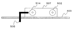
受信装置300の実装状態を示す図として、一方の面(表面)から見たものを図2に、他方の面(裏面)から見たものを図3に示す。本図に示すように受信装置300は、各種回路が搭載された第1の基板500と第2の基板501を有しており、これらの基板が金属製(導電性)で略直方体形状のシャーシ507に覆われる構成となっている。なお何れの基板も平板状(実装面が長方形)であり、互いの基板の所定の辺同士が向かい合うように、配置されている。
As a diagram showing the mounting state of the receiving
また第1の基板500には、チューナ回路部301とRFモジュレータ回路部310が配置されており、第2基板501には、デジタル復調回路部302、デジタル回路部304、電源部309、および映像音声出力回路311が配置されている。そして第1の基板500に配置されている各回路と第2の基板501に配置されている各回路とは、第1のシールド板508によって互いに分離されている。なお第2の基板501におけるより具体的な配置態様としては、第1の基板500と隣接する辺(図2における左側の辺)の側から、第2のコネクタ504、デジタル復調回路部302、電源部309、デジタル回路部304、映像音声出力回路311の順に配置されている。
In addition, a
チューナ入力端子502は、シャーシ507の枠部であって第2の基板に隣接しない側(図2の左側)に、シャーシ507から外向きへ垂直に突出するよう取り付けられており、第1の基板500上に配置されたチューナ回路部301に電気的に接続されている。また、第1の基板500は、シャーシ507に取り付けられており、チューナ回路部301のアナログアースパターンはシャーシ507に電気的に接続されている。また、第1の基板500において、チューナ入力端子502が取り付けられている辺と反対側の辺、つまり第2の基板501と対向している辺に臨むように、第2の基板501側との接続を実現するための第1のコネクタ503が配置されている。
The
なおシャーシ507は、第1の基板500と第2の基板501の表側の面に対向するように第1のフタが、同じく両基板の裏側の面に対向するように第2のフタが、それぞれ配置され、また第1のフタと第2のフタとの間においては、第1の基板500と第2の基板501を4枚の側壁で囲むように、枠部を有する構成となっている。これにより、第1の基板500と第2の基板501は、第1のフタと第2のフタを両底面とし枠部を側面とする、略直方体のシャーシ507の内部に収まる(端子の突出等は除く)態様となる。
The
RF出力端子514は、チューナ入力端子502と同様、シャーシ507の枠部であって第2の基板に隣接しない側から、外向きに垂直に突出するよう取り付けられており、第1の基板500上に配置されたRFモジュレータ回路部310に電気的に接続されている。また、RFモジュレータ回路部310のアナログアースパターンはシャーシ507に電気的に接続されている。また、チューナ回路部301とRFモジュレータ回路部310とは、第3のシールド板515によって互いに分離されている。
Similarly to the
また第2の基板において、第1の基板500と対向している辺に臨むように、第2のコネクタ504が配置されている。そして第1のコネクタ503と第2のコネクタ504は、互いにジャンパー510によって接続されている。そのため、第1の基板500と第2の基板501との接続を実現するための端子を、シャーシ507の外部に出す必要は無いものとなっている。これらのコネクタ(503、504)を介して、第1基板500側から第2基板501側への中間周波数の信号の伝送や、第2基板501側から第1基板500側へのアナログの映像および音声信号の伝送などがなされる。
In addition, the
また第2の基板501としては内層を有する多層基板が用いられており、デジタル回路部304の映像音声処理IC305と映像音声処理用メモリ306とを接続する配線が、内層パターン配置されている。一方で第1の基板500は、数十以上の多数のピンを持つICが搭載されておらず、第2の基板501に比べ少ない層数とすることが可能となっている。なお本実施形態の受信装置300では、第1の基板500は2層基板であり、第2の基板501は4層基板となっている。
A multilayer substrate having an inner layer is used as the
また第2の基板501において、映像音声出力回路311からRFモジュレータ回路部310へ向かって映像および音声信号を伝送するための配線(特に、映像音声出力回路311と第2のコネクタ504を結ぶ配線)は、内層パターンにて配置されている。なお、第1の基板500における回路と第2の基板501における回路を接続するジャンパー510の配列としては、第1の基板500側から第2の基板501側に向けて信号を伝送する配線と、第2の基板501側から第1の基板500側に向けて信号を伝送する配線との間に極力距離を設けられていることが好ましい。また、同じくこれらの配線同士の間に、アース接続するための配線が挿入されていることも好ましい。このようになっていることで、両配線を通る信号同士が混信したり、影響を及ぼし合ったりすることを極力回避することができる。
In the
また、第2の基板501のデジタル復調回路部302、デジタル回路部304のデジタルアースパターンはシャーシ507に電気的に接続されている。また第2の基板501においては、デジタル復調回路部302とその他の回路(デジタル回路部304、電源部309、および映像音声出力回路311)とは、第2のシールド板509によって互いに分離されている。
The digital
第1の基板500および第2の基板501のアースパターンとシャーシ507との接続は全て基板の片側の面(裏面)において、複数箇所のはんだ接続520〜527によって行われている。より具体的には、各基板(500、501)の全ての辺において行なわれている。また、第1のコネクタ503と第2のコネクタ504を接続するジャンパー510は、すべて基板の裏面側において、各コネクタ(503、504)にはんだ付けされることにより設けられている。
The ground patterns of the
このように、何れのはんだ接続も基板の片側の面(ここでは裏側の面)でなされているため、製造工程において、例えば各はんだ接続が同時にあるいは続いて行なわれる場合、はんだ接続の度に基板を裏返す必要性がなくなる。なお各基板(500、501)の実装面(表側の面と裏側の面)と、シャーシ(実装面を覆う部分)との距離は、裏側の面のもの方が、表側の面のものよりも小さくなっている。つまり裏側の方が、シャーシ側面の高さが低くなっている。そのためはんだ付け工程では、はんだ接続が裏側の面でなされることで、表側の面でなされる場合に比べ、はんだ付け装置や工具がシャーシ側面に接触する可能性を小さくことが可能となっている。 In this way, since any solder connection is made on one surface (here, the back surface) of the substrate, in the manufacturing process, for example, when each solder connection is performed simultaneously or subsequently, the substrate is connected at each solder connection. There is no need to turn it over. In addition, the distance between the mounting surface (front surface and back surface) of each substrate (500, 501) and the chassis (the portion covering the mounting surface) is larger on the back surface than on the front surface. It is getting smaller. In other words, the height of the chassis side is lower on the back side. Therefore, in the soldering process, it is possible to reduce the possibility that the soldering device or tool contacts the side surface of the chassis by making the solder connection on the back side surface, compared to the case where it is made on the front side surface. .
また、第2の基板501の一辺であって、第2のコネクタが配置されている辺と直交する辺(図2の上側の辺)には、この辺から外向きへ垂直に突出するように、第3のコネクタ505(上述したコネクタ315に相当するもの)が配置されている。つまり第3のコネクタ505は、チューナ入力端子502の軸に対して、直交する方向(L字となる方向)に突出していることになる。
In addition, one side of the
この第3のコネクタ505は、シャーシ507の外部にまで突出しており、第1の基板500や第2の基板に設けられている各回路を、映像表示装置400などの外部装置に接続可能としている。つまりチューナ入力端子502と第3のコネクタ505は、それぞれ略直方体であるシャーシ507から突出するように備えられており、シャーシ507におけるチューナ入力端子502が突出している面と、第3のコネクタ505が突出している面とは、互いに直交していることになる。また第3のコネクタ505は、可塑性の導電性材質で形成されており、外力を加えて折り曲げることが可能となっている。
The
第3のコネクタ505がこのように配置および構成されていることで、受信装置100と映像表示装置400との接続態様を、より状況に応じたものとすることが可能となっている。より具体的には、第3のコネクタ505を折り曲げないようにすることで、図4に示すように、映像表示装置400に対して受信装置100を立てて接続させることが可能となる。一方、第3のコネクタ505を直角に折り曲げることで、図5に示すように、映像表示装置400に対して受信装置を寝かせて接続させることが可能となる。
Since the
つまり、受信装置300における部品レイアウト等の設計変更を伴わずに、ピン状の第3のコネクタ505を折り曲げるだけで、両方の接続態様に対応することが可能となっている。なお、第3のコネクタ505と第2の基板501との接続は、該基板の裏面側における、はんだ接続によってなされている。
That is, it is possible to cope with both connection modes only by bending the pin-shaped
なお日本国内における地上波デジタル放送にはUHF帯が用いられているため、RFモジュレータ部310にてアナログの映像および音声信号を高周波に変換させるにあたっては、UHF帯以外の高周波に変換させることが好ましい。そこで本実施形態では、当該アナログの映像および音声信号を、VHF帯の高周波に変換させることとしている。このようにしておくことで、RFモジュレータ回路部310で生成されるRF出力信号が、チューナ回路部301にて受信されるデジタル放送信号に影響を与えることを、極力抑制することが可能となる。
Since the UHF band is used for terrestrial digital broadcasting in Japan, it is preferable to convert the analog video and audio signals to a high frequency other than the UHF band in the
また本実施形態では、受信装置100から映像表示装置400への映像および音声信号の出力として、コンポジット信号やステレオアナログ信号が用いられていない。そのため、アナログ放送チューナ回路部403においては、アナログ放送受信TVのコンポジット信号やステレオアナログ信号に係る端子が占有されることなく、デジタル放送に係る映像や音声信号を受けることが可能である。
In the present embodiment, no composite signal or stereo analog signal is used as the output of video and audio signals from the receiving
なお、例えばアナログ放送が停止されてデジタル放送のみとなった場合には、アナログ放送受信用のアンテナ入力端子が不要になるため、このアンテナ入力端子をデジタル放送に係る音声入力端子等として使用することが可能となる。 For example, when analog broadcasting is stopped and only digital broadcasting is performed, an antenna input terminal for receiving analog broadcasting is not required, so this antenna input terminal should be used as an audio input terminal for digital broadcasting. Is possible.
以上の通り本発明の一実施形態について説明したが、本発明の実施態様はこの内容に限定されるものではなく、本発明の主旨を逸脱しない限り、種々の改変を加えることが可能である。 Although one embodiment of the present invention has been described above, the embodiment of the present invention is not limited to this content, and various modifications can be made without departing from the gist of the present invention.
100 受信システム
200 アンテナ
301 チューナ回路部
302 デジタル復調回路部
303 デジタル復調IC
304 デジタル回路部
305 映像音声処理IC
306 映像音声処理用メモリ
307 プログラム用メモリ
308 制御マイコン
309 電源部
310 RFモジュレータ回路部
311 映像音声出力回路部
400 映像表示装置
401 表示処理部
402 音声処理部
403 アナログ放送チューナ回路部
500 第1の基板
501 第2の基板
502 チューナ入力端子
503 第1のコネクタ
504 第2のコネクタ
505 第3のコネクタ(入出力端子)
507 シャーシ
508 第1のシールド板
509 第2のシールド板
510 ジャンパー(ジャンパー線)
514 RF出力端子
520〜527 はんだ接続
DESCRIPTION OF
304
306 Video /
514 RF output terminal 520-527 Solder connection
Claims (19)
前記中間周波数の信号から、前記圧縮されたデジタルの映像または音声信号を抽出するデジタル復調回路部と、
該圧縮されたデジタルの映像または音声信号を、圧縮の解除されたデジタルの映像または音声信号に変換するデジタル回路部と、
該圧縮の解除されたデジタルの映像または音声信号を、アナログの映像または音声信号に変換する映像音声出力回路と、
該アナログの映像または音声信号を、高周波信号に変換するRFモジュレータ部と、
前記チューナ回路部、デジタル復調回路部、デジタル回路部、および映像音声出力回路に電力を供給する電源部と、を備えた受信装置であって、
前記チューナ回路部およびRFモジュレータ部は、所定の第1基板上に配置されて備えられている一方、
前記デジタル復調回路部、電源部、デジタル回路部、および映像音声出力回路は、内層を有する所定の第2基板上に配置されて備えられており、
該第2基板の内層には、前記映像音声出力回路から前記RFモジュレータ部に向かって前記アナログの映像または音声信号を伝送するための伝送路が配置されていることを特徴とする受信装置。 A tuner circuit unit that receives a high-frequency signal from a broadcasting station that broadcasts a high-frequency signal obtained by modulating a compressed digital video or audio signal, detects the signal at a predetermined frequency, and converts the signal into an intermediate-frequency signal;
A digital demodulation circuit unit for extracting the compressed digital video or audio signal from the intermediate frequency signal;
A digital circuit unit for converting the compressed digital video or audio signal into a decompressed digital video or audio signal;
A video / audio output circuit for converting the compressed digital video or audio signal into an analog video or audio signal;
An RF modulator for converting the analog video or audio signal into a high-frequency signal;
A power supply unit for supplying power to the tuner circuit unit, the digital demodulation circuit unit, the digital circuit unit, and the video / audio output circuit;
While the tuner circuit unit and the RF modulator unit are arranged and provided on a predetermined first substrate,
The digital demodulation circuit unit, the power supply unit, the digital circuit unit, and the video / audio output circuit are arranged and provided on a predetermined second substrate having an inner layer,
A receiving apparatus, wherein a transmission path for transmitting the analog video or audio signal from the video / audio output circuit toward the RF modulator section is disposed in an inner layer of the second substrate.
少なくとも第1辺を有する略平板形状であるとともに、前記第2基板と電気的に接続されるための第1コネクタが、該第1辺に臨むように設けられ、
前記第2基板は、
少なくとも第2辺を有する略平板形状であるとともに、前記第1基板と電気的に接続されるための第2コネクタが、該第2辺に臨むように設けられ、
該第1基板と第2基板は、
該第1辺と第2辺が対向するように配置されているとともに、
前記第1コネクタと第2コネクタが接続されることで、互いに電気的に接続されていることを特徴とする請求項1に記載の受信装置。 The first substrate is
A first connector having at least a first side and a first connector for being electrically connected to the second substrate, facing the first side;
The second substrate is
A substantially flat plate shape having at least a second side, and a second connector for being electrically connected to the first substrate is provided to face the second side,
The first substrate and the second substrate are:
The first side and the second side are arranged to face each other, and
The receiving apparatus according to claim 1, wherein the first connector and the second connector are connected to each other so as to be electrically connected to each other.
前記第1コネクタおよび第2コネクタを介して、前記チューナ回路部から前記デジタル復調回路部に伝送されることを特徴とする請求項2に記載の受信装置。 The intermediate frequency signal is:
The receiving apparatus according to claim 2, wherein the receiving device is transmitted from the tuner circuit unit to the digital demodulation circuit unit via the first connector and the second connector.
前記第1基板における層の数は、該第2基板における層の数よりも、少ないことを特徴とする請求項3に記載の受信装置。 While the second substrate is a multilayer substrate having three or more layers,
The receiving device according to claim 3, wherein the number of layers in the first substrate is smaller than the number of layers in the second substrate.
前記第2辺からその対辺に向かって、前記デジタル復調回路部、電源部、デジタル回路部、映像音声出力回路の順に配置されていることを特徴とする請求項2に記載の受信装置。 In the digital demodulation circuit unit, the power supply unit, the digital circuit unit, and the video / audio output circuit, the arrangement mode on the second substrate,
The receiving apparatus according to claim 2, wherein the digital demodulating circuit unit, the power supply unit, the digital circuit unit, and the video / audio output circuit are arranged in this order from the second side toward the opposite side.
前記第1基板におけるアースパターンと前記第2基板におけるアースパターンは、共に該シャーシに接続されることで、互いに電気的に接続されていることを特徴とする請求項2に記載の受信装置。 The first substrate and the second substrate are provided to be covered with a chassis formed of a conductive material,
The receiving apparatus according to claim 2, wherein the ground pattern on the first substrate and the ground pattern on the second substrate are both electrically connected to each other by being connected to the chassis.
前記第2基板におけるアースパターンは、デジタル回路のアースとして用いられるものであることを特徴とする請求項7に記載の受信装置。 While the ground pattern on the first substrate is used as an analog circuit ground,
The receiving apparatus according to claim 7, wherein the ground pattern on the second substrate is used as a ground of a digital circuit.
該第1はんだ接続は、
該各基板の片側の面でなされることを特徴とする請求項7に記載の受信装置。 The connection between the ground pattern and the chassis on each of the substrates is made by solder connection (referred to as “first solder connection”),
The first solder connection is:
The receiving apparatus according to claim 7, wherein the receiving apparatus is formed on one side of each substrate.
前記各基板における面のうち、前記シャーシとの距離が小さい方の面においてなされることを特徴とする請求項9に記載の受信装置。 The first solder connection is:
The receiving apparatus according to claim 9, wherein the receiving apparatus is formed on a surface having a smaller distance from the chassis among the surfaces of the substrates.
各基板の複数の辺にてなされていることを特徴とする請求項9または請求項10に記載の受信装置。 The first solder connection is:
The receiving apparatus according to claim 9, wherein the receiving apparatus is formed on a plurality of sides of each substrate.
各基板の全ての辺にてなされていることを特徴とする請求項11に記載の受信装置。 The first solder connection is:
The receiving apparatus according to claim 11, wherein the receiving apparatus is formed on all sides of each substrate.
該第2はんだ接続は、
前記各基板の片側の面でなされることを特徴とする請求項2に記載の受信装置。 The first connector and the second connector are both connected to each other by making a solder connection with a jumper wire (referred to as “second solder connection”).
The second solder connection is
The receiving apparatus according to claim 2, wherein the receiving apparatus is formed on one side of each substrate.
該第2はんだ接続は、
前記各基板における面のうち、前記第1はんだ接続がなされている面でなされることを特徴とする請求項9に記載の受信装置。 The first connector and the second connector are both connected to each other by making a solder connection with a jumper wire (referred to as “second solder connection”).
The second solder connection is
The receiving device according to claim 9, wherein the receiving device is formed on a surface of the substrates on which the first solder connection is made.
該入出力端子は、前記第2はんだ接続がなされている面において、前記第2基板にはんだ接続されていることを特徴とする請求項14に記載の受信装置。 It has an input / output terminal to input / output signals to / from the outside.
The receiving device according to claim 14, wherein the input / output terminal is solder-connected to the second substrate on a surface where the second solder connection is made.
前記チューナ回路部に外部から前記高周波信号を入力させるためのチューナ入力端子、および前記入出力端子が、それぞれ該シャーシから突出するように備えられており、
前記シャーシにおける該チューナ入力端子が突出している面と、該入出力端子が突出している面とは、互いに直交していることを特徴とする請求項15に記載の受信装置。 The first substrate and the second substrate are disposed inside a substantially rectangular parallelepiped chassis,
A tuner input terminal for inputting the high-frequency signal from the outside to the tuner circuit unit, and the input / output terminal are provided so as to protrude from the chassis, respectively.
The receiving device according to claim 15, wherein a surface of the chassis from which the tuner input terminal protrudes and a surface from which the input / output terminal protrudes are orthogonal to each other.
前記アナログの映像または音声信号を、VHF帯の高周波信号に変換することを特徴とする請求項1から請求項16の何れかに記載の受信装置。 The RF modulator section is
The receiving apparatus according to any one of claims 1 to 16, wherein the analog video or audio signal is converted into a high-frequency signal in a VHF band.
該デジタルの映像または音声信号を、アナログの映像または音声信号に変換する映像音声出力回路と、
前記映像音声出力回路から、所定の伝送路を通じて前記アナログの映像または音声信号を受取り、高周波信号に変換するRFモジュレータ部と、を備え、
前記映像音声出力回路は、内層を有する基板上に配置されて備えられており、
前記伝送路は、該内層に配置されていることを特徴とする受信装置。 A receiver for receiving broadcast waves related to digital video or audio signals;
A video / audio output circuit for converting the digital video or audio signal into an analog video or audio signal;
An RF modulator unit that receives the analog video or audio signal from the video / audio output circuit through a predetermined transmission path and converts the analog video or audio signal into a high-frequency signal;
The video / audio output circuit is provided on a substrate having an inner layer,
The receiving apparatus, wherein the transmission path is arranged in the inner layer.
Priority Applications (1)
| Application Number | Priority Date | Filing Date | Title |
|---|---|---|---|
| JP2007258376A JP2009089214A (en) | 2007-10-02 | 2007-10-02 | Digital broadcast receiving apparatus |
Applications Claiming Priority (1)
| Application Number | Priority Date | Filing Date | Title |
|---|---|---|---|
| JP2007258376A JP2009089214A (en) | 2007-10-02 | 2007-10-02 | Digital broadcast receiving apparatus |
Publications (1)
| Publication Number | Publication Date |
|---|---|
| JP2009089214A true JP2009089214A (en) | 2009-04-23 |
Family
ID=40661975
Family Applications (1)
| Application Number | Title | Priority Date | Filing Date |
|---|---|---|---|
| JP2007258376A Pending JP2009089214A (en) | 2007-10-02 | 2007-10-02 | Digital broadcast receiving apparatus |
Country Status (1)
| Country | Link |
|---|---|
| JP (1) | JP2009089214A (en) |
-
2007
- 2007-10-02 JP JP2007258376A patent/JP2009089214A/en active Pending
Similar Documents
| Publication | Publication Date | Title |
|---|---|---|
| JP4350084B2 (en) | Receiver and receiver system | |
| JP4063841B2 (en) | Receiving device, receiving system | |
| US5710999A (en) | Radio frequency apparatus | |
| JP4338710B2 (en) | Receiver and receiver system | |
| JP4066269B2 (en) | Receiving device, receiving system | |
| JP2007251702A (en) | Receiving apparatus, receiving system | |
| US20070216814A1 (en) | Receiver apparatus and receiver system | |
| WO2011081058A1 (en) | Tuner module and receiver | |
| JP2008219456A (en) | Receiving system | |
| JP2009089214A (en) | Digital broadcast receiving apparatus | |
| TWI521874B (en) | Tuner | |
| JP4562718B2 (en) | Receiving apparatus and receiving system | |
| JPH11317687A (en) | Electronic tuner | |
| US20120314385A1 (en) | Circuit board and electronic apparatus | |
| JP4157835B2 (en) | Cable modem module device, cable modem device, and broadcast receiving device | |
| KR100755609B1 (en) | A set top box having direct connection for modules | |
| JP2008011065A (en) | Receiver and receiving system | |
| JP2009302796A (en) | Receiver, and receiving system | |
| JP2009296426A (en) | Electric equipment, converter for satellite broadcasting reception, and antenna device for satellite broadcasting reception | |
| JP2006157484A (en) | Digital broadcast receiving unit | |
| JP2008113120A (en) | Reception module, reception device, and television receiver | |
| JP4584233B2 (en) | Reception device and reception noise reduction method thereof | |
| JP2008131359A (en) | Receiving apparatus and system | |
| JP2008294758A (en) | High frequency receiver | |
| JP2011071670A (en) | Receiving module and receiver including the same |