JP2007182009A - Manufacturing method for nozzle base plate, liquid droplet ejection head and liquid droplet ejector - Google Patents
Manufacturing method for nozzle base plate, liquid droplet ejection head and liquid droplet ejector Download PDFInfo
- Publication number
- JP2007182009A JP2007182009A JP2006002321A JP2006002321A JP2007182009A JP 2007182009 A JP2007182009 A JP 2007182009A JP 2006002321 A JP2006002321 A JP 2006002321A JP 2006002321 A JP2006002321 A JP 2006002321A JP 2007182009 A JP2007182009 A JP 2007182009A
- Authority
- JP
- Japan
- Prior art keywords
- nozzle
- substrate
- manufacturing
- droplet discharge
- etching
- Prior art date
- Legal status (The legal status is an assumption and is not a legal conclusion. Google has not performed a legal analysis and makes no representation as to the accuracy of the status listed.)
- Withdrawn
Links
Images


Landscapes
- Particle Formation And Scattering Control In Inkjet Printers (AREA)
Abstract
Description
本発明は、微細加工によってノズルが形成されるノズル基板、インク等の液滴の吐出を行う液滴吐出ヘッド、液滴吐出装置の製造方法に関するものである。 The present invention relates to a nozzle substrate on which nozzles are formed by microfabrication, a droplet discharge head that discharges droplets of ink or the like, and a method for manufacturing a droplet discharge device.
例えばシリコン等を加工して微小な素子等を形成する微細加工技術(MEMS:Micro Electro Mechanical Systems)が急激な進歩を遂げている。微細加工技術により形成される微細加工素子の例としては、例えば液滴吐出方式のプリンタのような記録(印刷)装置で用いられている液滴吐出ヘッド(インクジェットヘッド)、マイクロポンプ、光可変フィルタ、モータのような静電アクチュエータ、圧力センサ等がある。 For example, micro electro mechanical systems (MEMS) that process silicon or the like to form microelements and the like have made rapid progress. Examples of microfabricated elements formed by microfabrication technology include, for example, a droplet discharge head (inkjet head), a micropump, and an optical variable filter used in a recording (printing) apparatus such as a droplet discharge type printer. There are electrostatic actuators such as motors, pressure sensors and the like.
ここで、微細加工素子の一例として液滴吐出ヘッドについて説明する。液滴吐出方式の記録(印刷)装置は、家庭用、工業用を問わず、あらゆる分野の印刷に利用されている。液滴吐出方式とは、例えば複数のノズルを有する液滴吐出ヘッドを対象物(紙等)との間で相対移動させ、対象物の所定の位置に液滴を吐出させて印刷等をするものである。この方式は、液晶(Liquid Crystal)を用いた表示装置を作製する際のカラーフィルタ、有機化合物等の電界発光(ElectroLuminescence )素子を用いた表示パネル(OLEDs)、DNA、タンパク質等、生体分子のマイクロアレイ等の製造にも利用されている。 Here, a droplet discharge head will be described as an example of a microfabricated element. A droplet discharge type recording (printing) apparatus is used for printing in various fields regardless of whether it is for home use or industrial use. The droplet discharge method is, for example, a method in which a droplet discharge head having a plurality of nozzles is moved relative to an object (paper, etc.), and a droplet is discharged to a predetermined position of the object for printing or the like. It is. This system is a microarray of biomolecules such as color filters for producing display devices using liquid crystals, display panels (OLEDs) using electroluminescent devices such as organic compounds, DNA, proteins, etc. Etc. are also used in the manufacture of
液滴吐出ヘッドによりノズルから液滴を吐出させる方法については、例えば液体を加熱し、発生した空気(気泡)の圧力で液滴を吐出させるものがある。また、液体をためておく吐出室を流路の一部に備え、吐出室の少なくとも一面の壁(ここでは、底部の壁とし、以下、この壁のことを振動板ということにする)を撓ませて(動作させて)形状変化により吐出室内の圧力を高め、連通するノズルから液滴を吐出させる方法がある。さらに振動板を可動電極とし、振動板と距離を空けて対向する電極(固定電極)との間に電圧を印加させ、発生する静電気力(静電引力を用いることが多いので、以下、静電引力とする)を利用し、発生させた静電引力により振動板を変位させてその圧力により吐出させるものもある(例えば特許文献1参照)。 As a method of ejecting droplets from a nozzle by a droplet ejection head, for example, there is a method in which a liquid is heated and droplets are ejected by the pressure of generated air (bubbles). Also, a discharge chamber for storing liquid is provided in a part of the flow path, and at least one wall of the discharge chamber (here, referred to as a bottom wall, hereinafter referred to as a diaphragm) is bent. There is a method in which (in operation) the pressure in the discharge chamber is increased by shape change, and droplets are discharged from the communicating nozzle. In addition, the diaphragm is a movable electrode, a voltage is applied between the electrode (fixed electrode) facing the diaphragm at a distance, and the generated electrostatic force (electrostatic attractive force is often used. In some cases, the diaphragm is displaced by the generated electrostatic attraction force and discharged by the pressure (see, for example, Patent Document 1).
ここで、液体を液滴として吐出するためのノズルを有するノズル基板について考えてみる。ノズル基板は、主に異方性エッチングによる加工を基板に行って作製する。異方性エッチングとして、ドライエッチング(乾式エッチング)、ウェットエッチング(湿式エッチング)がある。通常、一方の面側からドライエッチングを行ってノズルの形状を形成しておき、他方の面からウェットエッチングを行ってノズルが貫通するまでエッチングを行うという工程が採られることが多い。ここで、吐出性能を高めるため、ノズルの形状は、テーパ形状に近い、2段以上の段状に形成することが多い。 Here, consider a nozzle substrate having nozzles for ejecting liquid as droplets. The nozzle substrate is manufactured by performing processing on the substrate mainly by anisotropic etching. As anisotropic etching, there are dry etching (dry etching) and wet etching (wet etching). In general, a process is often employed in which dry etching is performed from one surface side to form a nozzle shape, and wet etching is performed from the other surface until etching is performed through the nozzle. Here, in order to improve discharge performance, the shape of the nozzle is often formed in two or more steps that are close to a tapered shape.
このとき、ウェットエッチングを行う部分以外の部分(特にドライエッチングにより形成したノズル部分)をエッチングしてしまわないように、ウェットエッチングを行う部分以外の部分を耐エッチング保護膜(例えば酸化シリコン膜)で保護する。 At this time, in order not to etch the portion other than the portion where wet etching is performed (particularly the nozzle portion formed by dry etching), the portion other than the portion where wet etching is performed is an etching resistant protective film (for example, a silicon oxide film). Protect.
しかしながら、基板に対して垂直にドライエッチングされて形成されたノズルの内側において、例えばエッジ部分等、耐エッチング保護膜を所望の厚みで均一に成膜するのは非常に困難である。そのため、例えば吐出側の開口部分の成膜が不均一であると、ウェットエッチングにより貫通させた際に開口部分に影響を与えることがある。例えば異方性ウェットエッチングでは結晶面方位を利用するが、面方位の影響を受け、開口部分周辺が平面に形成されないことがある。これにより、ノズルから吐出された液滴の吐出性能が低くなる(例えば吐出方向が直進しない(斜めになる)等)ことがある。また、吐出性能が低すぎると、そのノズル基板を用いることができないため、これにより歩留まりの低下を招いてしまうおそれがあった。 However, it is very difficult to uniformly form an anti-etching protective film with a desired thickness inside a nozzle formed by dry etching perpendicularly to the substrate, for example, an edge portion. Therefore, for example, if the film formation on the discharge-side opening is not uniform, the opening may be affected when the film is penetrated by wet etching. For example, crystal orientation is used in anisotropic wet etching, but the periphery of the opening may not be formed in a plane due to the influence of the surface orientation. Thereby, the discharge performance of the liquid droplets discharged from the nozzles may be lowered (for example, the discharge direction does not go straight (becomes slanted)). Also, if the discharge performance is too low, the nozzle substrate cannot be used, which may lead to a decrease in yield.
そこで、本発明はこのような問題を解決するため、所望のノズル形状を形成することができるノズル基板の製造方法を得ることを目的とする。また、そのノズル基板に基づく液滴吐出ヘッド等の製造方法を得ることを目的とする。 Accordingly, an object of the present invention is to obtain a nozzle substrate manufacturing method capable of forming a desired nozzle shape in order to solve such a problem. Another object of the present invention is to obtain a method for manufacturing a droplet discharge head or the like based on the nozzle substrate.
本発明に係るノズル基板の製造方法は、シリコン基板の一方の面側からノズルの供給口を開口するとともに、ノズルとなる凹部を形成する工程と、ノズルとなる凹部を形成した面と反対側の面から異方性ドライエッチングによるエッチングを行って凹部に穴を空け、ノズルの吐出口を形成する工程とを有するものである。
本発明によれば、ノズル基板を製造する際、ノズルを貫通させて吐出口を開口するために最終的に行うエッチングを異方性ドライエッチングにより行うようにしたので、吐出口の開口部分周辺に、例えば結晶面による凹凸が形成されることなく、平坦に形成することができ、吐出性能が高いノズル基板を製造することができ、さらには歩留まりも高くすることができる。
The nozzle substrate manufacturing method according to the present invention includes a step of opening a nozzle supply port from one surface side of a silicon substrate, forming a recess serving as a nozzle, and a surface opposite to the surface where the recess serving as a nozzle is formed. And a step of performing etching by anisotropic dry etching from the surface to form a hole in the recess and forming a discharge port of the nozzle.
According to the present invention, when the nozzle substrate is manufactured, the etching finally performed to open the discharge port through the nozzle is performed by anisotropic dry etching. For example, it can be formed flat without forming irregularities due to crystal planes, a nozzle substrate with high discharge performance can be manufactured, and the yield can also be increased.
また、本発明に係るノズル基板の製造方法は、ノズルとなる凹部を形成した面と反対側の面から、所望の厚さになるまで異方性ウェットエッチングを行った後、異方性ドライエッチングにより吐出口を開口形成するものである。
本発明によれば、異方性ドライエッチングを行う前に、異方性ウェットエッチングによりエッチングを行うようにしたので、複数のウェハを一度に処理することができ、時間も短縮することができるので、生産性を高めることができる。
In addition, the method for manufacturing a nozzle substrate according to the present invention includes anisotropic wet etching after performing anisotropic wet etching from the surface opposite to the surface on which the concave portion serving as the nozzle is formed to a desired thickness. Thus, the discharge port is formed as an opening.
According to the present invention, since anisotropic wet etching is performed before anisotropic dry etching, a plurality of wafers can be processed at one time, and the time can be shortened. , Can increase productivity.
また、本発明に係るノズル基板の製造方法は、所望の厚さを10μm以上に設定するものである。
本発明によれば、所望の厚さを10μm以上に設定しておくことにより、例えば、異方性ウェットエッチングによる進行状態のばらつきが生じたとしても、ウェットエッチングの段階で吐出孔となる孔を開口させてしまうことがなく、吐出性能の高いノズル基板を製造することができる。
Moreover, the manufacturing method of the nozzle substrate which concerns on this invention sets desired thickness to 10 micrometers or more.
According to the present invention, by setting the desired thickness to 10 μm or more, for example, even if variation in the progress state due to anisotropic wet etching occurs, the holes that become discharge holes at the wet etching stage are formed. A nozzle substrate with high discharge performance can be manufactured without opening.
また、本発明に係るノズル基板の製造方法は、吐出口が供給口よりも小さな口径となるような、テーパ状又は階段状のノズルを形成するものである。
本発明によれば、ノズルの形状がテーパ状又は階段状になるように形成するようにしたので、より確実に吐出した液滴を直進させることができる等、吐出性能の高いノズル基板を製造することができる。
Moreover, the nozzle substrate manufacturing method according to the present invention forms a tapered or stepped nozzle such that the discharge port has a smaller diameter than the supply port.
According to the present invention, since the nozzle is formed so as to have a tapered shape or a stepped shape, a nozzle substrate having high ejection performance can be manufactured, for example, the ejected liquid droplets can be straightened more reliably. be able to.
また、本発明に係る液滴吐出ヘッドの製造方法は、上記の方法で製造したノズル基板と、ノズル基板が有するノズルに液体を供給するための流路と、流路の一部に液体を加圧する加圧手段とを備えた基板とを接合する工程を有するものである。
本発明によれば、上記の製造方法で製造したノズル基板を用いて液滴吐出ヘッドを製造するようにしたので、吐出性能が高い液滴吐出ヘッドを製造することができる。また、歩留まりも高くすることができる。
In addition, the method for manufacturing a droplet discharge head according to the present invention includes a nozzle substrate manufactured by the above method, a channel for supplying liquid to the nozzles of the nozzle substrate, and a liquid added to a part of the channel. And a step of bonding a substrate provided with a pressing means for pressing.
According to the present invention, since the droplet discharge head is manufactured using the nozzle substrate manufactured by the above manufacturing method, it is possible to manufacture a droplet discharge head with high discharge performance. In addition, the yield can be increased.
また、本発明に係る液滴吐出装置の製造方法は、上記の液滴吐出ヘッドの製造方法を適用して液滴吐出装置を製造するものである。
本発明によれば、上記の製造方法で製造した液滴吐出ヘッドを用いて液滴吐出装置を製造するようにしたので、吐出性能が高い装置を製造することができる。また、歩留まりも高くすることができる。
In addition, a method for manufacturing a droplet discharge device according to the present invention is a method for manufacturing a droplet discharge device by applying the method for manufacturing a droplet discharge head described above.
According to the present invention, since the droplet discharge device is manufactured using the droplet discharge head manufactured by the above manufacturing method, a device having high discharge performance can be manufactured. In addition, the yield can be increased.
実施の形態1.
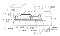
図1は本発明の第1の実施の形態に係る液滴吐出ヘッドを分解して表した図である。図1は静電アクチュエータの代表として、フェイスイジェクト型の液滴吐出ヘッドを表している(なお、構成部材を図示し、見やすくするため、図1を含め、以下の図面では各構成部材の大きさの関係が実際のものと異なる場合がある。また、図の上側を上とし、下側を下として説明する)。図1において、電極基板10は厚さ約1mmであり、図1では、キャビティ基板20の下面に、振動板22と対向して接合される。本実施の形態では、電極基板10を構成する基板として硼珪酸系の耐熱硬質ガラスを材料とする。電極基板10には、キャビティ基板20に形成される各吐出室21に合わせ、例えば深さ約0.25μmの溝部11を設け、その内側(特に底部)に各吐出室22と対向する個別電極12A、リード部12B及び端子部12C(以下、特に区別しないときはこれらを合わせて電極部12という)を設けている。本実施の形態では、電極部12の材料として、酸化錫を不純物としてインジウムにドープしたITO(Indium Tin Oxide:インジウム錫酸化物)を用い、例えばスパッタ等により溝部11の底面に例えば0.1μmの厚さで成膜する。液体供給口13は、外部のタンク(図示せず)から液滴吐出ヘッドにインク等の液体を供給するための取り入れ口となる。
FIG. 1 is an exploded view of a droplet discharge head according to a first embodiment of the present invention. FIG. 1 shows a face eject type liquid droplet ejection head as a representative of an electrostatic actuator. (For the sake of clarity, the components are shown in the following drawings including FIG. May be different from the actual relationship, and the upper side of the figure is the upper side and the lower side is the lower side). In FIG. 1, the
キャビティ基板20は、例えば表面が(110)面方位のシリコン単結晶基板(この基板を含め、以下、単にシリコン基板という)を材料としている。キャビティ基板20には、吐出室21となる凹部(底壁が被駆動部となる振動板22となる)及び各ノズル共通に吐出する液体を貯めておくためのリザーバ23となる凹部を形成している。凹部の形成には、例えば異方性ウェットエッチング法(以下、ウェットエッチングという)を用いる。リザーバ23は液体供給口13を介して供給される液体を一旦貯め、各吐出室22に液体を供給する。また、キャビティ基板1上に設けられた共通電極端子24は、電極部12に供給される電荷とは反対の電荷をキャビティ基板20に供給するためのものである。また、個別電極12Aと振動板22とを絶縁させるため、振動板22の下面には絶縁膜25が成膜されている。
The cavity substrate 20 is made of, for example, a silicon single crystal substrate whose surface has a (110) plane orientation (including this substrate, hereinafter, simply referred to as a silicon substrate). The cavity substrate 20 is formed with a recess serving as the discharge chamber 21 (the bottom wall serves as the vibration plate 22 serving as the driven portion) and a recess serving as the reservoir 23 for storing the liquid ejected in common to each nozzle. Yes. For example, an anisotropic wet etching method (hereinafter referred to as wet etching) is used to form the recess. The reservoir 23 temporarily stores the liquid supplied via the liquid supply port 13 and supplies the liquid to each discharge chamber 22. The common electrode terminal 24 provided on the
ノズル基板30は、本実施の形態では、例えば厚さ約200μmのシリコン基板を用いられ、電極基板10とは反対の面(図1の場合には上面)でキャビティ基板20と接合されている。本実施の形態のノズル基板30は、吐出室21と連通する、2段で形成されたノズル31を複数有しているものとする。ノズル基板30の外側(図1の場合には上面)の面で円形になるように開口した、液体の吐出側となる小さい方の口径(約20μm)の口(ノズル吐出口31A−1とする)を有する円柱状のノズルを第1ノズル31Aとする。また、内側(キャビティ基板20と対向する面、図1の場合には下面)の面で円形になるように開口した、液体の供給側になる大きい方の口径(約50μm)の口(ノズル供給口31B−1とする)を有する円柱状のノズルを第2ノズル31Bとする。ここで第1ノズル31Aと第2ノズル31Bにより形成される円の中心は同じ(同心円)であるとする。また、内側の面にはオリフィス32となる細溝を設け、吐出室21とリザーバ23とを連通させ、リザーバ23に溜めた液体を吐出室21に供給するための連通溝とする。ダイヤフラム33は、振動板22の加圧により、リザーバ23に溜められた液体に伝播する力を緩衝するために設けられている。なお、図1ではノズル基板30が上面となり、電極基板20を下面としているが、実際に用いられる場合には、通常、ノズル基板30の方が電極基板20よりも下面となる。 In the present embodiment, for example, a silicon substrate having a thickness of about 200 μm is used as the nozzle substrate 30, and the nozzle substrate 30 is bonded to the cavity substrate 20 on the surface opposite to the electrode substrate 10 (upper surface in the case of FIG. 1). The nozzle substrate 30 of the present embodiment is assumed to have a plurality of nozzles 31 formed in two stages that communicate with the discharge chamber 21. A small opening (approximately 20 μm) on the liquid discharge side (referred to as nozzle discharge port 31A-1) opened to be circular on the outer surface (upper surface in the case of FIG. 1) of the nozzle substrate 30. ) Is a first nozzle 31A. In addition, an opening (nozzle supply) having a larger diameter (approximately 50 μm) on the liquid supply side, opened to be circular on the inner surface (the surface facing the cavity substrate 20, the lower surface in FIG. 1). A cylindrical nozzle having a mouth 31B-1 is referred to as a second nozzle 31B. Here, it is assumed that the centers of the circles formed by the first nozzle 31A and the second nozzle 31B are the same (concentric circles). In addition, a narrow groove serving as an orifice 32 is provided on the inner surface, and the discharge chamber 21 and the reservoir 23 are communicated with each other to serve as a communication groove for supplying the liquid stored in the reservoir 23 to the discharge chamber 21. The diaphragm 33 is provided to buffer the force propagating to the liquid accumulated in the reservoir 23 by pressurizing the diaphragm 22. In FIG. 1, the nozzle substrate 30 is the upper surface and the electrode substrate 20 is the lower surface. However, in actual use, the nozzle substrate 30 is usually the lower surface than the electrode substrate 20.
図2は液滴吐出ヘッドの断面図である。端子部12Cは電極取出し口26において、外部に露出している。そして、発振回路41は、直接又はワイヤ、FPC(Flexible Print Circuit)等の配線42を介して電気的に端子部12C、共通電極端子24と接続され、個別電極12A、キャビティ基板20(振動板22)に電荷(電力)の供給及び停止を制御する回路である。発振回路41は、例えば24kHzで発振し、個別電極12Aに例えば0Vと30Vのパルス電圧を印加して電荷供給を行う。発振回路41が発振駆動し、各個別電極12Aに選択的に電荷を供給して正に帯電させ、また、振動板22を相対的に負に帯電させる。このとき、静電気力により振動板22は個別電極12Aに引き寄せられて撓む。これにより吐出室21の容積は広がる。電荷供給を止めると振動板22は元に戻るが、そのとき吐出室21の容積も元に戻り、その圧力により液滴が吐出する。この液滴が例えば吐出対象物に着弾して印刷等が行われる。端子部12Cを外部に露出させることで、個別電極12Aと振動板22との間の空間(ギャップ)が外気と連通するのを防ぐために、封止材27により封止及び外気の遮断をしている。 FIG. 2 is a cross-sectional view of the droplet discharge head. The terminal portion 12 </ b> C is exposed to the outside at the electrode outlet 26. The oscillation circuit 41 is electrically connected to the terminal portion 12C and the common electrode terminal 24 directly or via a wire 42 such as a wire or FPC (Flexible Print Circuit), and the individual electrode 12A, the cavity substrate 20 (the diaphragm 22). ) Is a circuit for controlling supply and stop of electric charge (electric power). The oscillation circuit 41 oscillates at, for example, 24 kHz, and supplies charges by applying pulse voltages of, for example, 0 V and 30 V to the individual electrode 12A. The oscillation circuit 41 oscillates and drives the individual electrodes 12A selectively to charge them positively and to charge the diaphragm 22 relatively negatively. At this time, the diaphragm 22 is attracted to the individual electrode 12A by the electrostatic force and bent. This increases the volume of the discharge chamber 21. When the charge supply is stopped, the diaphragm 22 returns to its original state, but at that time, the volume of the discharge chamber 21 also returns to its original state, and droplets are discharged by the pressure. For example, printing is performed by the droplets landing on an ejection target. In order to prevent the space (gap) between the individual electrode 12A and the diaphragm 22 from communicating with the outside air by exposing the terminal portion 12C to the outside, the sealing material 27 is used to seal and block the outside air. Yes.
本実施の形態では、ノズル基板30について、ウェットエッチングによってノズル形状を変形させることなく設計通りに作製することにより、吐出性能が高いノズル基板30、ノズル基板30を有する液滴吐出ヘッドを得るものである。そこで、従来、ある面に異方性ドライエッチング法(以下、ドライエッチングという)でノズル31の形状を形成した後、その反対の面からウェットエッチングを行ってノズル吐出口31A−1を開口形成し、ノズル31を貫通形成していたものを、貫通させる前の段階で、例えばウェットエッチングからドライエッチングに切り換えてエッチングを行い、最終的にドライエッチングにより開口、貫通させるようにする。これにより、ノズル31の吐出側の開口部分周辺を平面に保つようにして吐出性能を高める。 In the present embodiment, the nozzle substrate 30 is manufactured as designed without changing the nozzle shape by wet etching, so that the nozzle substrate 30 having high ejection performance and a droplet ejection head having the nozzle substrate 30 are obtained. is there. Therefore, conventionally, after the shape of the nozzle 31 is formed on a certain surface by anisotropic dry etching (hereinafter referred to as dry etching), the nozzle discharge port 31A-1 is formed by performing wet etching from the opposite surface. In the stage before penetrating the nozzle 31 that has been formed to penetrate, etching is performed by switching from wet etching to dry etching, for example, and finally the opening and penetration are performed by dry etching. Thus, the discharge performance is enhanced by keeping the periphery of the opening portion on the discharge side of the nozzle 31 flat.
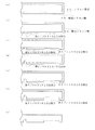
図3及び図4は実施の形態1のノズル基板30の作製方法を表す図である。次に図3及び図4に基づいて、本発明におけるノズル基板30の作製方法の手順について説明する。なお、実際には、シリコンウェハから複数個分の液滴吐出ヘッドのノズル基板30を同時形成するが、図3及び図4ではその一部分だけを示している。 3 and 4 are diagrams illustrating a method for manufacturing the nozzle substrate 30 according to the first embodiment. Next, based on FIG.3 and FIG.4, the procedure of the manufacturing method of the nozzle substrate 30 in this invention is demonstrated. Actually, a plurality of nozzle substrates 30 of droplet discharge heads are simultaneously formed from a silicon wafer, but only a part of them is shown in FIGS.
まず、厚さ約200μmのシリコン基板51に、エッチングを行う際、シリコン基板51を保護するための膜(レジスト)となる酸化シリコン膜52を例えば約1.2μm成膜する(図3(a))。成膜方法については特に限定しないが、ここでは、例えば、高温(約1075℃)で酸素及び水蒸気雰囲気中にシリコン基板51を晒して成膜する熱酸化による方法を用いる。ここでシリコン基板51として、表面が(100)面方位のシリコン基板を用いるものとする。 First, when etching is performed on a silicon substrate 51 having a thickness of about 200 μm, a silicon oxide film 52 serving as a film (resist) for protecting the silicon substrate 51 is formed, for example, about 1.2 μm (FIG. 3A). ). The film forming method is not particularly limited, but here, for example, a method by thermal oxidation in which the silicon substrate 51 is exposed to an oxygen and water vapor atmosphere at a high temperature (about 1075 ° C.) is used. Here, as the silicon substrate 51, a silicon substrate having a (100) plane orientation is used.
そして、酸化シリコン膜52を選択的にエッチングしてパターニングを行うため、フォトリソグラフィ法を用い、レジスト膜となる感光剤を塗布し、露光、現像により、第1ノズル31Aとなる部分のレジスト膜を除去する。そして、例えばフッ酸水溶液、緩衝フッ酸水溶液(BHF:例えばフッ酸水溶液とフッ化アンモニウム水溶液とを1:6で混合した液体)等に浸積し、第1ノズル31Aとなる部分の酸化シリコン膜52をエッチングにより除去してシリコンを露出させる(図3(b))。 Then, in order to perform patterning by selectively etching the silicon oxide film 52, a photolithography method is used to apply a photosensitive agent to be a resist film, and a portion of the resist film to be the first nozzle 31A is formed by exposure and development. Remove. Then, for example, a silicon oxide film in a portion to be the first nozzle 31A is immersed in a hydrofluoric acid aqueous solution, a buffered hydrofluoric acid aqueous solution (BHF: for example, a liquid in which a hydrofluoric acid aqueous solution and an ammonium fluoride aqueous solution are mixed at 1: 6) or the like. 52 is removed by etching to expose the silicon (FIG. 3B).
さらに、第2ノズル31B(ノズル供給口31B−1)となる部分及びオリフィス32となる部分の酸化シリコン膜52について、ハーフエッチングによる除去を行う。除去方法については第1ノズル31Aとなる部分の場合と同様であるが、第2ノズル31Bとなる部分及びオリフィス32となる部分については、少し酸化シリコン膜52を残すため、シリコンが露出していない(図3(c))。次に、ドライエッチングを行い、第1ノズル31Aの部分に対して、例えば口径約20μm、深さ約50μmの凹部(孔)を形成する(図3(d))。ドライエッチングの種類等については特に限定しないが、例えばICP(Inductively Coupled Plasma)放電によるドライエッチングを行うようにしてもよい。この場合、エッチングに用いるガスとして、例えばフッ素系のC4 F8 (クタフルオロシクロブタン)で側壁面の保護を行いつつ、SF6 (6フッ化硫黄)で深さ方向へのエッチングを交互に繰り返し、ドライエッチングを行う。そして、フォトリソグラフィ法等により、ハーフエッチングにより残されていた第2ノズル31Bとなる部分及びオリフィス32となる部分の酸化シリコン膜52を除去する(図3(e))。 Further, the silicon oxide film 52 in the portion that becomes the second nozzle 31B (nozzle supply port 31B-1) and the portion that becomes the orifice 32 is removed by half etching. The removal method is the same as in the case of the portion that becomes the first nozzle 31A, but the silicon oxide film 52 is left slightly in the portion that becomes the second nozzle 31B and the portion that becomes the orifice 32, so that silicon is not exposed. (FIG. 3C). Next, dry etching is performed to form a recess (hole) having a diameter of about 20 μm and a depth of about 50 μm, for example, in the first nozzle 31A (FIG. 3D). The type of dry etching or the like is not particularly limited. For example, dry etching by ICP (Inductively Coupled Plasma) discharge may be performed. In this case, the etching is alternately repeated in the depth direction with SF 6 (sulfur hexafluoride) while protecting the side wall surface with, for example, fluorine-based C 4 F 8 (Kutafluorocyclobutane) as a gas used for etching. Then, dry etching is performed. Then, the silicon oxide film 52 in the portion that becomes the second nozzle 31B and the portion that becomes the orifice 32 left by the half etching is removed by a photolithography method or the like (FIG. 3E).
そして、ドライエッチングを行い、第2ノズル31Bの部分に対して口径約50μm、深さ50μmの凹部(孔)を形成する。第1ノズル31Aの部分についてはさらに50μm深い部分まで凹部が形成される。また、ドライエッチングによりオリフィス32も同時に形成する(図3(f))。ここでもドライエッチングの種類等については特に限定しない。ドライエッチングが終了すると、保護膜として成膜していた酸化シリコン膜52を除去する(図3(g))。酸化シリコン膜52の除去は、例えば前述したフッ酸水溶液等で全面をウェットエッチングすることで行う。そして、さらにウェットエッチングを行うための保護膜として酸化シリコン膜53を全面に成膜する(図3(h))。成膜の方法については特に限定しないが、ここでは、凹凸に関係なく成膜することができる熱酸化法を用いる。酸化シリコン膜53の成膜後、また、フォトリソグラフィ法を用い、酸化シリコン膜53において、ノズル31を貫通形成するための凹部34となる部分及びダイヤフラム33となる部分をウェットエッチングにより除去してシリコンを露出させる(図3(i))。 Then, dry etching is performed to form a recess (hole) having a diameter of about 50 μm and a depth of 50 μm with respect to the second nozzle 31B. About the part of the 1st nozzle 31A, a recessed part is further formed to a part deep 50 micrometers. Further, the orifice 32 is simultaneously formed by dry etching (FIG. 3F). Again, the type of dry etching is not particularly limited. When the dry etching is completed, the silicon oxide film 52 formed as a protective film is removed (FIG. 3G). The removal of the silicon oxide film 52 is performed, for example, by wet etching the entire surface with the hydrofluoric acid aqueous solution described above. Then, a silicon oxide film 53 is formed on the entire surface as a protective film for further wet etching (FIG. 3H). There is no particular limitation on the method for forming the film, but here, a thermal oxidation method capable of forming a film regardless of unevenness is used. After the formation of the silicon oxide film 53, and using a photolithography method, the silicon oxide film 53 is removed by wet etching to remove the portion that will become the recess 34 and the portion that will become the diaphragm 33 for penetrating the nozzle 31. Is exposed (FIG. 3I).
次にシリコン基板をエッチング液に浸積し、凹部34となる部分及びダイヤフラム33となる部分をウェットエッチングする(図3(j))。シリコンのウェットエッチングには、例えば32w%の濃度の水酸化カリウム(KOH)水溶液等を用いる。ここで、通常、このウェットエッチングによってノズル31を貫通形成させてしまうが、本実施の形態においては貫通形成させずに残す。残す厚さについては特に限定しないが、本実施の形態では、エッチングの進行状態にばらつきがあることを考慮し、約10μmの厚さが残るような時間管理を行うようにする。 Next, the silicon substrate is immersed in an etching solution, and the portion that becomes the concave portion 34 and the portion that becomes the diaphragm 33 are wet-etched (FIG. 3J). For the wet etching of silicon, for example, a potassium hydroxide (KOH) aqueous solution having a concentration of 32 w% is used. Here, normally, the nozzle 31 is formed through by this wet etching, but in this embodiment, it is left without being formed through. The remaining thickness is not particularly limited, but in this embodiment, time management is performed so that a thickness of about 10 μm remains in consideration of variations in the progress of etching.
さらに、凹部34となる部分及びダイヤフラム33となる部分についてドライエッチングを行う(図3(k))。これにより、第1ノズル31Aとして形成された凹部の一部に穴が空いて開口することで、ノズル31が貫通形成される(ただ酸化シリコン膜53は残されている)。さらにダイヤフラム33が形成される。ドライエッチングが終了すると、保護膜として成膜していた酸化シリコン膜53を除去する(図3(l))。これにより最終的にノズル吐出口31A−1が開口し、ノズル31が貫通する。さらに、耐インク保護及び絶縁のための酸化シリコン膜54を全面に成膜する(図3(m))。ここでは、前述の熱酸化法により成膜するようにするが、例えばTEOS(ここでは、Tetraethyl orthosilicate Tetraethoxysilane:テトラエトキシシラン(珪酸エチル))を用いてプラズマCVD(Chemical Vapor Deposition:TEOS−pCVDともいう)法により酸化シリコン膜を形成するようにしてもよい。また、絶縁膜として例えばAl2O3(酸化アルミニウム(アルミナ))のような別の材料を用いてもよい。 Further, dry etching is performed on the portion that becomes the recess 34 and the portion that becomes the diaphragm 33 (FIG. 3K). As a result, a hole is opened in a part of the concave portion formed as the first nozzle 31 </ b> A, thereby forming the nozzle 31 so as to penetrate (only the silicon oxide film 53 remains). Further, a diaphragm 33 is formed. When dry etching is completed, the silicon oxide film 53 formed as a protective film is removed (FIG. 3L). As a result, the nozzle discharge port 31A-1 is finally opened, and the nozzle 31 penetrates. Further, a silicon oxide film 54 for protecting ink and insulating is formed on the entire surface (FIG. 3 (m)). Here, the film is formed by the above-described thermal oxidation method. For example, TEOS (here, Tetraethyl orthosilicate Tetraethoxysilane) is also referred to as plasma CVD (Chemical Vapor Deposition: TEOS-pCVD). ) Method may be used to form a silicon oxide film. Further, another material such as Al 2 O 3 (aluminum oxide (alumina)) may be used as the insulating film.
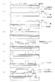
図5は液滴吐出ヘッドの製造工程を表す図である。図5に基づいて他の基板の作製をはじめとする液滴吐出ヘッド製造工程について説明する。なお、実際には、シリコンウェハから複数個分の液滴吐出ヘッドの部材を同時形成するが、図5ではその一部分だけを示している。 FIG. 5 is a diagram illustrating a manufacturing process of the droplet discharge head. Based on FIG. 5, a manufacturing process of a droplet discharge head including manufacturing of another substrate will be described. In practice, a plurality of droplet discharge head members are simultaneously formed from a silicon wafer, but only a part thereof is shown in FIG.
電極基板10となる約1mmのガラスの基板の一方の面に対し、電極部12の形状パターンに合わせて0.2μmの深さの溝部11を形成する。そして、例えばスパッタ等の方法を用いて、0.1μmの厚さのITOを溝部11の内側(特に底壁)に成膜し、電極部12を形成する。さらに液体供給口13をサンドブラスト法または切削加工により形成する。これにより、ガラス基板10が作製される(図5(a))。
A groove 11 having a depth of 0.2 μm is formed in accordance with the shape pattern of the electrode portion 12 on one surface of a glass substrate of about 1 mm to be the
キャビティ基板20となる基板については、まず例えば表面が(110)面方位の酸素濃度の低いシリコン基板61の片面を鏡面研磨し、220μmの厚みにする。次に、シリコン基板61にボロンドープ層62を形成する面を、B2 O3 を主成分とする固体の拡散源に対向させて石英ボートにセットする。さらに縦型炉に石英ボートをセットして、炉内を窒素雰囲気にし、例えば、温度を1050℃に上昇させて7時間保持してボロンをシリコン基板61中に拡散させ、ボロンドープ層62を形成する。このとき、ボロンドープ層62の表面にはボロン化合物が形成されているが(図示なし)、酸素及び水蒸気雰囲気中、600℃の条件で1時間30分酸化することで、フッ酸水溶液によるエッチングが可能なB2O3+SiO2 に化学変化させ、フッ酸水溶液にてウェットエッチングして除去する。そして、さらにボロンドープ層62を形成した面に、プラズマCVD法により絶縁膜25を成膜する(図5(b))。絶縁膜25は、例えばプラズマCVD法により、成膜時の処理温度を360℃、高周波出力を250W、圧力は66.7Pa(0.5Torr)、ガス流量をTEOS流量100cm3 /min(100sccm)、酸素流量1000cm3 /min(1000sccm)の条件で0.1μm成膜する。 For the substrate to be the cavity substrate 20, first, for example, one surface of the silicon substrate 61 having a low oxygen concentration with a (110) plane orientation is mirror-polished to a thickness of 220 μm. Next, the surface on which the boron-doped layer 62 is formed on the silicon substrate 61 is set on a quartz boat so as to face a solid diffusion source mainly composed of B 2 O 3 . Further, a quartz boat is set in a vertical furnace, and the inside of the furnace is made into a nitrogen atmosphere. For example, the temperature is raised to 1050 ° C. and held for 7 hours to diffuse boron into the silicon substrate 61 to form a boron doped layer 62. . At this time, a boron compound is formed on the surface of the boron dope layer 62 (not shown), but etching with a hydrofluoric acid aqueous solution is possible by oxidizing for 1 hour 30 minutes in an oxygen and water vapor atmosphere at 600 ° C. It is chemically changed to B 2 O 3 + SiO 2 and removed by wet etching with a hydrofluoric acid aqueous solution. Further, an insulating film 25 is formed on the surface on which the boron doped layer 62 is formed by plasma CVD (FIG. 5B). The insulating film 25 is formed by plasma CVD, for example, at a processing temperature of 360 ° C., a high frequency output of 250 W, a pressure of 66.7 Pa (0.5 Torr), a gas flow rate of TEOS flow rate 100 cm 3 / min (100 sccm), A 0.1 μm film is formed under the condition of an oxygen flow rate of 1000 cm 3 / min (1000 sccm).
次にシリコン基板61と電極基板10を360℃に加熱した後、電極基板10に負極、シリコン基板71に正極を接続して、800Vの電圧を印加して陽極接合を行う。そして、陽極接合後の接合済み基板において、シリコン基板61の厚みが約60μmになるまでシリコン基板61表面の研削加工を行う。その後、加工変質層を除去するために、例えば32w%の濃度の水酸化カリウム溶液でシリコン基板61を約10μmウェットエッチングする。これによりシリコン基板61の厚みを約50μmにする(図5(c))。
Next, after heating the silicon substrate 61 and the
ウェットエッチングを行った面に対し、例えばエッチングマスクとなる酸化シリコン膜63を、TEOSによるプラズマCVD法で成膜する。酸化シリコン膜63の成膜条件としては、例えば、成膜時の処理温度は360℃、高周波出力は700W、圧力は33.3Pa(0.25Torr)、ガス流量はTEOS流量100cm3 /min(100sccm)、酸素流量1000cm3 /min(1000sccm)の条件で1.5μm成膜する。TEOSを用いた成膜は比較的低温で行うことができ、基板の加熱をできる限り抑えられる。さらに、フォトリソグラフィ法を用い、酸化シリコン膜63において、吐出室21、リザーバ23及び電極取出し口26となる部分をエッチングにより除去する(図5(d))。ここで、例えば吐出室21及び電極取出し口26となる部分についてはシリコンを露出させ、リザーバ23についてはハーフエッチングにより酸化シリコン膜63を残す。これはリザーバ23となる部分についてはシリコンを残すことにより、剛性を持たせるようにするためである。 For example, a silicon oxide film 63 serving as an etching mask is formed on the wet etched surface by a plasma CVD method using TEOS. The deposition conditions of the silicon oxide film 63 include, for example, a processing temperature of 360 ° C., a high frequency output of 700 W, a pressure of 33.3 Pa (0.25 Torr), and a gas flow rate of TEOS flow rate 100 cm 3 / min (100 sccm). ), And a film thickness of 1.5 μm is formed under the condition of oxygen flow rate of 1000 cm 3 / min (1000 sccm). Film formation using TEOS can be performed at a relatively low temperature, and heating of the substrate can be suppressed as much as possible. Further, using the photolithography method, the portions that become the discharge chamber 21, the reservoir 23, and the electrode outlet 26 in the silicon oxide film 63 are removed by etching (FIG. 5D). Here, for example, silicon is exposed in portions that become the discharge chamber 21 and the electrode outlet 26, and the silicon oxide film 63 is left in the reservoir 23 by half etching. This is because the portion that becomes the reservoir 23 is made rigid by leaving silicon.
次に、接合済み基板を35wt%の濃度の水酸化カリウム水溶液に浸し、吐出室21となる部分の厚みが約10μmになるまでウェットエッチングを行う。さらに、接合済み基板を3wt%の濃度の水酸化カリウム水溶液に浸し、ボロンドープ層62において、エッチングストップが十分効いたものと判断するまでエッチングを続ける。このように、前記2種類の濃度の異なる水酸化カリウム水溶液を用いたウェットエッチングを行うことによって、形成される振動板22の面荒れを抑制し、厚み精度を0.80±0.05μm以下にすることができる。その結果、液滴吐出ヘッドの吐出性能を安定化することができる(図5(e))。ウェットエッチングを終了すると、接合済み基板を例えばフッ酸水溶液に浸し、シリコン基板61表面の酸化シリコン膜63を除去する(図5(f))。 Next, the bonded substrate is immersed in a 35 wt% potassium hydroxide aqueous solution, and wet etching is performed until the thickness of the portion that becomes the discharge chamber 21 becomes about 10 μm. Further, the bonded substrate is immersed in a 3 wt% potassium hydroxide aqueous solution, and etching is continued until it is determined that the etching stop is sufficiently effective in the boron doped layer 62. Thus, by performing wet etching using the two types of potassium hydroxide aqueous solutions having different concentrations, the surface roughness of the diaphragm 22 to be formed is suppressed, and the thickness accuracy is 0.80 ± 0.05 μm or less. can do. As a result, the discharge performance of the droplet discharge head can be stabilized (FIG. 5E). When the wet etching is finished, the bonded substrate is immersed in a hydrofluoric acid aqueous solution, for example, and the silicon oxide film 63 on the surface of the silicon substrate 61 is removed (FIG. 5F).
シリコン基板71の電極取出し口26となる部分のシリコン(ボロンドープ層72)を除去し、開口する。除去の方法については、特に限定しないが、例えばピン等で突いて壊すこともできる。また、ドライエッチングを行って開口することもできる。その後、電極取出し口26の端部にあるキャビティ基板20と各凹部11との間で形成されるギャップの開口部に沿って、例えばエポキシ樹脂を流し込んだり、酸化シリコンを堆積等させたりして封止材27を形成して封止し、ギャップを外気から遮断する(図5(g))。ここで、特に図示はしないが、例えば、キャビティ基板20の上面に、液体保護のための酸化シリコン膜を、例えばTEOSを用い、プラズマCVD法により形成するようにしてもよい。 The silicon (boron doped layer 72) in the portion that becomes the electrode outlet 26 of the silicon substrate 71 is removed and opened. The removal method is not particularly limited. For example, it can be broken by a pin or the like. Moreover, it can also open by performing dry etching. Thereafter, sealing is performed by pouring, for example, epoxy resin or depositing silicon oxide along the opening of the gap formed between the cavity substrate 20 and each recess 11 at the end of the electrode outlet 26. The stop material 27 is formed and sealed, and the gap is blocked from the outside air (FIG. 5G). Here, although not particularly illustrated, for example, a silicon oxide film for protecting the liquid may be formed on the upper surface of the cavity substrate 20 by plasma CVD using TEOS, for example.
封止が完了すると、例えば、共通電極端子24となる部分を開口したマスクを、接合基板のシリコン基板71側の表面に取り付ける。そして、例えばプラチナ(Pt)をターゲットとしてスパッタ等を行い、共通電極端子24を形成する。そして、別工程で作製した前述のノズル基板30を、例えばエポキシ系接着剤により、接合基板のキャビティ基板20側から接着し、接合する(図5(h))。そして、ダイシングラインに沿ってダイシングを行い、個々の液滴吐出ヘッドに切断し、液滴吐出ヘッドが完成する。 When the sealing is completed, for example, a mask having an opening at a portion to be the common electrode terminal 24 is attached to the surface of the bonding substrate on the silicon substrate 71 side. Then, for example, sputtering is performed using platinum (Pt) as a target to form the common electrode terminal 24. Then, the above-described nozzle substrate 30 produced in a separate process is bonded and bonded from the cavity substrate 20 side of the bonding substrate, for example, with an epoxy adhesive (FIG. 5H). Then, dicing is performed along the dicing line, and cutting into individual droplet discharge heads is completed.
以上のように実施の形態1によれば、ノズル基板30に関して、ノズル31を貫通させ、ノズル吐出口1A−1を開口するために最終的に行うエッチングを、ドライエッチングにより行うようにしたので、ノズル31の開口部分周辺を凹凸なく、平坦に形成することができる。そのため、吐出性能を高めることができ、歩留まりも高くすることができる。また、ドライエッチングを行う前にウェットエッチングも併用して凹部54となる部分及びダイヤフラム33となる部分のエッチングを行うようにしたので、複数のウェハを一度に処理することができ、また時間も短縮することができるので、生産性を高めることができる。これにより、このノズル基板30を用いて製造する液滴吐出ヘッドの品質を高めることができる。
As described above, according to the first embodiment, with respect to the nozzle substrate 30, the etching finally performed to penetrate the nozzle 31 and open the
実施の形態2.
上述の実施の形態では、凹部54となる部分及びダイヤフラム33となる部分についてエッチングを行う際、ウェットエッチングとドライエッチングとを併用して行う工程とした。本発明はこれに限定するものではなく、全てをドライエッチングの工程で行うようにしてもよい。この場合、ウェットエッチングによる結晶面方位の影響を受けないため、例えば同時に形成するダイヤフラム33の設計の自由度を高め、例えばダイヤフラム33の面積を広くとることができる。
Embodiment 2. FIG.
In the above-described embodiment, when etching is performed on the portion to be the concave portion 54 and the portion to be the diaphragm 33, the process is performed using both wet etching and dry etching. The present invention is not limited to this, and all may be performed in a dry etching process. In this case, since it is not affected by the crystal plane orientation due to wet etching, for example, the degree of freedom in designing the diaphragm 33 formed simultaneously can be increased, and for example, the area of the diaphragm 33 can be increased.
実施の形態3.
上述の実施の形態における液滴吐出ヘッドは、電極基板10、キャビティ基板20及びノズル基板30の3つの基板を積層して構成したが、本発明はこれに限定するものではない。例えば、リザーバ23の容積を大きくするため、リザーバ23となる凹部を独立した基板に形成し、4つの基板を積層した構成の液滴吐出ヘッドについても適用することができる。
Embodiment 3 FIG.
The droplet discharge head in the above-described embodiment is configured by laminating three substrates of the
上述の実施の形態では、振動板22と個別電極12との間に発生する静電力により振動板22を変位させて液体を加圧し、ノズル31から液滴を吐出させる液滴吐出ヘッドについて説明した。本発明はこれに限定するものではない。例えば、気体を発生させたり、圧電素子を用いる等、他の加圧方法による液滴吐出ヘッドについても適用することができる。 In the above-described embodiment, the liquid droplet discharge head that pressurizes the liquid by displacing the vibration plate 22 by the electrostatic force generated between the vibration plate 22 and the individual electrode 12 and discharges the liquid droplets from the nozzle 31 has been described. . The present invention is not limited to this. For example, the present invention can also be applied to a droplet discharge head using another pressurization method such as generating gas or using a piezoelectric element.
実施の形態4.
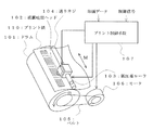
図6は上述の実施の形態で製造した液滴吐出ヘッドを用いた液滴吐出装置の外観図である。また、図7は液滴吐出装置の主要な構成手段の一例を表す図である。図6及び図7の液滴吐出装置は液滴吐出方式(インクジェット方式)による印刷を目的とする。また、いわゆるシリアル型の装置である。図12において、被印刷物であるプリント紙100が支持されるドラム101と、プリント紙100にインクを吐出し、記録を行う液滴吐出ヘッド102とで主に構成される。また、図示していないが、液滴吐出ヘッド102にインクを供給するためのインク供給手段がある。プリント紙110は、ドラム101の軸方向に平行に設けられた紙圧着ローラ103により、ドラム101に圧着して保持される。そして、送りネジ104がドラム101の軸方向に平行に設けられ、液滴吐出ヘッド102が保持されている。送りネジ104が回転することによって液滴吐出ヘッド102がドラム101の軸方向に移動するようになっている。
Embodiment 4 FIG.
FIG. 6 is an external view of a droplet discharge apparatus using the droplet discharge head manufactured in the above embodiment. FIG. 7 is a diagram illustrating an example of main constituent means of the droplet discharge device. 6 and 7 is intended for printing by a droplet discharge method (inkjet method). Further, it is a so-called serial type device. In FIG. 12, a drum 101 that supports a printing paper 100 that is a substrate to be printed and a droplet discharge head 102 that discharges ink to the printing paper 100 and performs recording are mainly configured. Although not shown, there is an ink supply means for supplying ink to the droplet discharge head 102. The print paper 110 is held by being pressed against the drum 101 by a paper press roller 103 provided parallel to the axial direction of the drum 101. A feed screw 104 is provided parallel to the axial direction of the drum 101, and the droplet discharge head 102 is held. As the feed screw 104 rotates, the droplet discharge head 102 moves in the axial direction of the drum 101.
一方、ドラム101は、ベルト105等を介してモータ106により回転駆動される。また、プリント制御手段107は、印画データ及び制御信号に基づいて送りネジ104、モータ106を駆動させ、また、ここでは図示していないが、発振駆動回路を駆動させて振動板22を振動させ、制御をしながらプリント紙110に印刷を行わせる。 On the other hand, the drum 101 is rotationally driven by a motor 106 via a belt 105 or the like. Further, the print control unit 107 drives the feed screw 104 and the motor 106 based on the print data and the control signal, and although not shown here, drives the oscillation drive circuit to vibrate the diaphragm 22, Printing is performed on the print paper 110 while controlling.
ここでは液体をインクとしてプリント紙110に吐出するようにしているが、液滴吐出ヘッドから吐出する液体はインクに限定されない。例えば、カラーフィルタとなる基板に吐出させる用途においては、カラーフィルタ用の顔料を含む液体、OLED等の表示基板に吐出させる用途においては、発光素子となる化合物を含む液体、基板上に配線する用途においては、例えば導電性金属を含む液体を、それぞれの装置において設けられた液滴吐出ヘッドから吐出させるようにしてもよい。また、液滴吐出ヘッドをディスペンサとし、生体分子のマイクロアレイとなる基板に吐出する用途に用いる場合では、DNA(Deoxyribo Nucleic Acids :デオキシリボ核酸)、他の核酸(例えば、Ribo Nucleic Acid:リボ核酸、Peptide Nucleic Acids:ペプチド核酸等)タンパク質等のプローブを含む液体を吐出させるようにしてもよい。その他、布等の染料の吐出等にも利用することができる。 Here, the liquid is ejected onto the print paper 110 as ink, but the liquid ejected from the droplet ejection head is not limited to ink. For example, in an application to be discharged onto a substrate to be a color filter, a liquid containing a pigment for a color filter, an application to be discharged to a display substrate such as an OLED, an application to be wired on a substrate, a liquid containing a compound to be a light emitting element In this case, for example, a liquid containing a conductive metal may be discharged from a droplet discharge head provided in each device. In addition, when the droplet discharge head is used as a dispenser and is used for discharging onto a substrate that is a microarray of biomolecules, DNA (Deoxyribo Nucleic Acids: deoxyribonucleic acid), other nucleic acids (for example, Ribo Nucleic Acid: ribonucleic acid, Peptide (Nucleic Acids: peptide nucleic acids, etc.) A liquid containing a probe such as a protein may be discharged. In addition, it can also be used for discharging dyes such as cloth.
10 電極基板、11 溝部、12 電極部、12A 個別電極、12B リード部、12C 端子部、13 液体供給口、20 キャビティ基板、21 吐出室、22 振動板、23 リザーバ、24 共通電極端子、25 絶縁膜、26 電極取出し口、27 封止材、30 ノズル基板、31 ノズル、31A 第1ノズル、31A−1 ノズル吐出口、31B 第2ノズル、31B−1 ノズル供給口、32 オリフィス、33 ダイヤフラム、34 凹部、41 発振回路、42 配線、61 シリコン基板、62ボロンドープ層、63 酸化シリコン膜、100 プリンタ、101 ドラム、102 液滴吐出ヘッド、103 紙圧着ローラ、104 送りネジ、105 ベルト、106 モータ、107 プリント制御手段、110 プリント紙。
10 electrode substrate, 11 groove portion, 12 electrode portion, 12A individual electrode, 12B lead portion, 12C terminal portion, 13 liquid supply port, 20 cavity substrate, 21 discharge chamber, 22 diaphragm, 23 reservoir, 24 common electrode terminal, 25 insulation Membrane, 26 Electrode outlet, 27 Sealing material, 30 Nozzle substrate, 31 Nozzle, 31A First nozzle, 31A-1 Nozzle outlet, 31B Second nozzle, 31B-1 Nozzle supply port, 32 Orifice, 33 Diaphragm, 34 Recess, 41 Oscillation circuit, 42 wiring, 61 silicon substrate, 62 boron doped layer, 63 silicon oxide film, 100 printer, 101 drum, 102 droplet discharge head, 103 paper pressure roller, 104 feed screw, 105 belt, 106 motor, 107 Print control means, 110 print paper.
Claims (6)
前記ノズルとなる凹部を形成した面と反対側の面から異方性ドライエッチングによるエッチングを行って前記凹部に穴を空け、前記ノズルの吐出口を形成する工程と
を有することを特徴とするノズル基板の製造方法。 Opening the nozzle supply port from one side of the silicon substrate and forming a recess to be a nozzle;
A nozzle having a step of performing etching by anisotropic dry etching from a surface opposite to a surface on which the concave portion serving as the nozzle is formed to form a hole in the concave portion and forming a discharge port of the nozzle. A method for manufacturing a substrate.
該ノズル基板が有する前記ノズルに液体を供給するための流路と、該流路の一部に液体を加圧する加圧手段とを備えた基板とを接合する工程を有することを特徴とする液滴吐出ヘッドの製造方法。 A nozzle substrate manufactured by the method according to claim 1;
A liquid comprising: a step of bonding a flow path for supplying a liquid to the nozzle of the nozzle substrate and a substrate provided with a pressurizing means for pressurizing the liquid to a part of the flow path. A method for manufacturing a droplet discharge head.
A method for manufacturing a droplet discharge device, wherein the droplet discharge device is manufactured by applying the method for manufacturing a droplet discharge head according to claim 5.
Priority Applications (1)
| Application Number | Priority Date | Filing Date | Title |
|---|---|---|---|
| JP2006002321A JP2007182009A (en) | 2006-01-10 | 2006-01-10 | Manufacturing method for nozzle base plate, liquid droplet ejection head and liquid droplet ejector |
Applications Claiming Priority (1)
| Application Number | Priority Date | Filing Date | Title |
|---|---|---|---|
| JP2006002321A JP2007182009A (en) | 2006-01-10 | 2006-01-10 | Manufacturing method for nozzle base plate, liquid droplet ejection head and liquid droplet ejector |
Publications (1)
| Publication Number | Publication Date |
|---|---|
| JP2007182009A true JP2007182009A (en) | 2007-07-19 |
Family
ID=38338483
Family Applications (1)
| Application Number | Title | Priority Date | Filing Date |
|---|---|---|---|
| JP2006002321A Withdrawn JP2007182009A (en) | 2006-01-10 | 2006-01-10 | Manufacturing method for nozzle base plate, liquid droplet ejection head and liquid droplet ejector |
Country Status (1)
| Country | Link |
|---|---|
| JP (1) | JP2007182009A (en) |
Cited By (2)
| Publication number | Priority date | Publication date | Assignee | Title |
|---|---|---|---|---|
| JP2009061663A (en) * | 2007-09-06 | 2009-03-26 | Canon Inc | Manufacturing method of inkjet head substrate |
| JP2009248444A (en) * | 2008-04-07 | 2009-10-29 | Seiko Epson Corp | Nozzle substrate formed of silicon, liquid droplet delivering head, liquid droplet delivering apparatus, method for manufacturing nozzle substrate formed of silicon, method for manufacturing liquid droplet delivering head, and method for manufacturing liquid droplet delivering apparatus |
-
2006
- 2006-01-10 JP JP2006002321A patent/JP2007182009A/en not_active Withdrawn
Cited By (2)
| Publication number | Priority date | Publication date | Assignee | Title |
|---|---|---|---|---|
| JP2009061663A (en) * | 2007-09-06 | 2009-03-26 | Canon Inc | Manufacturing method of inkjet head substrate |
| JP2009248444A (en) * | 2008-04-07 | 2009-10-29 | Seiko Epson Corp | Nozzle substrate formed of silicon, liquid droplet delivering head, liquid droplet delivering apparatus, method for manufacturing nozzle substrate formed of silicon, method for manufacturing liquid droplet delivering head, and method for manufacturing liquid droplet delivering apparatus |
Similar Documents
| Publication | Publication Date | Title |
|---|---|---|
| JP2007152621A (en) | Liquid droplet jet head and method for manufacturing the same | |
| JP2007038629A (en) | Electrostatic actuator, liquid droplet discharge head, liquid droplet discharge apparatus, electrostatic device, and those manufacturing methods | |
| JP4379421B2 (en) | Electrostatic actuator, droplet discharge head, droplet discharge apparatus, and method for manufacturing electrostatic drive device | |
| JP5612819B2 (en) | Nozzle substrate, droplet discharge head, and manufacturing method of droplet discharge apparatus | |
| JP4259554B2 (en) | Method for manufacturing droplet discharge head and method for manufacturing droplet discharge device | |
| JP2007182009A (en) | Manufacturing method for nozzle base plate, liquid droplet ejection head and liquid droplet ejector | |
| JP2008279707A (en) | Manufacturing method for nozzle substrate, liquid droplet ejection head and liquid droplet ejector | |
| JP2010120169A (en) | Nozzle substrate, method for manufacturing liquid droplet ejecting head and liquid droplet ejecting apparatus, the liquid droplet ejecting head, and the liquid droplet ejecting apparatus | |
| JP2010142991A (en) | Nozzle substrate, liquid droplet delivery head, liquid droplet delivery device, and method of manufacturing those | |
| JP2008114319A (en) | Manufacturing method of electrostatic actuator, droplet discharge head, droplet discharger, and electrostatic device | |
| JP2007318870A (en) | Electrostatic actuator, droplet discharge head, droplet discharger, electrostatic device, and their manufacturing method | |
| JP2007143342A (en) | Electrostatic actuator, droplet discharge head and droplet discharge device, and manufacturing method thereof | |
| US20080252695A1 (en) | Droplet discharge head, droplet discharge device, and discharge controlling method thereof | |
| JP2007326195A (en) | Electrode substrate, electrostatic actuator, droplet discharging head, droplet discharging device, electrostatic drive device, and manufacturing method of those | |
| JP2006198820A (en) | Actuator, electrostatic actuator, droplet discharge head and electrostatic actuator manufacturing method | |
| JP2009119699A (en) | Mask substrate, its manufacturing method, liquid droplet ejection head, and manufacturing method of liquid droplet ejection device | |
| JP2008132646A (en) | Liquid droplet ejection head and manufacturing method for liquid ejector | |
| JP2008093941A (en) | Nozzle substrate, method for manufacturing droplet discharge head and droplet discharge device, droplet discharge head, and droplet discharge device | |
| JP2010214922A (en) | Nozzle substrate, liquid droplet ejecting head, liquid droplet ejection device, and method for manufacturing nozzle substrate | |
| JP2007190730A (en) | Mask substrate, its manufacturing method, liquid droplet ejection head, and method for manufacturing liquid droplet ejection device | |
| JP2008254391A (en) | Electrostatic actuator, electrostatic drive device, liquid-droplet discharge head, and manufacturing method for liquid-droplet discharge device | |
| JP2010115828A (en) | Nozzle substrate, liquid droplet ejecting head, liquid droplet ejecting apparatus, and method for manufacturing the same | |
| JP2008179093A (en) | Method for manufacturing liquid droplet discharge head | |
| JP4701935B2 (en) | Method for manufacturing droplet discharge head | |
| JP2006264216A (en) | Electrostatic actuator, droplet ejection head, droplet ejection device, electrostatic device, and method of producing them |
Legal Events
| Date | Code | Title | Description |
|---|---|---|---|
| A300 | Withdrawal of application because of no request for examination |
Free format text: JAPANESE INTERMEDIATE CODE: A300 Effective date: 20090407 |